ICGOO在线商城 > 隔离器 > 光隔离器 - 晶体管,光电输出 > 4N25VM

 Datasheet下载
- 型号: 4N25VM
- 制造商: Fairchild Semiconductor
- 库位|库存: xxxx|xxxx
- 要求:
| 数量阶梯 | 香港交货 | 国内含税 |
| +xxxx | $xxxx | ¥xxxx |
查看当月历史价格
查看今年历史价格
4N25VM产品简介:
ICGOO电子元器件商城为您提供4N25VM由Fairchild Semiconductor设计生产,在icgoo商城现货销售,并且可以通过原厂、代理商等渠道进行代购。 4N25VM价格参考。Fairchild Semiconductor4N25VM封装/规格:光隔离器 - 晶体管,光电输出, 光隔离器 有基极的晶体管 输出 4170Vrms 1 通道 6-DIP。您可以下载4N25VM参考资料、Datasheet数据手册功能说明书,资料中有4N25VM 详细功能的应用电路图电压和使用方法及教程。
4N25VM 是一款由 ON Semiconductor 提供的光隔离器(光电耦合器),属于光隔离器 - 晶体管类别,采用光电输出设计。它通过光信号传输实现输入与输出之间的电气隔离,广泛应用于需要高抗干扰能力、低噪声和安全隔离的场景。以下是其主要应用场景:

1. 工业控制
   4N25VM 常用于工业自动化设备中,例如 PLC(可编程逻辑控制器)、继电器驱动电路和传感器接口。它能够有效隔离输入信号与控制电路,防止高压或噪声干扰影响系统稳定性。

2. 通信设备
   在通信系统中,该器件可用于信号隔离,确保数据传输的可靠性和安全性。例如,在 RS-232 或 RS-485 接口电路中,使用 4N25VM 可以避免地环路问题和电磁干扰。

3. 电源管理
   在开关电源、稳压器或 DC-DC 转换器中,4N25VM 可用于反馈信号的隔离传输,确保主电路与控制电路之间的电气隔离,提高系统的安全性和效率。

4. 医疗设备
   医疗仪器(如心电图机、监护仪等)对电气安全要求极高。4N25VM 可用于隔离患者接触部分与设备主电路,防止漏电流对患者造成伤害。

5. 音频和视频设备
   在音频功放、视频切换器等设备中,4N25VM 可用于信号隔离,减少噪声干扰,提升音视频质量。

6. 电机驱动与逆变器
   在电机控制和逆变器电路中,4N25VM 可用于隔离控制信号与功率级电路,保护微控制器或其他敏感元件免受高压冲击。

7. 家用电器
   在一些高端家电(如洗衣机、空调等)中,4N25VM 可用于隔离用户界面与主控板之间的信号,增强系统的抗干扰能力。

总结来说,4N25VM 的典型应用场景集中在需要电气隔离、信号传输和抗干扰能力的领域,特别适合低速信号传输和中小功率应用场合。
| 参数 | 数值 |
| 产品目录 | |
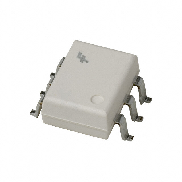
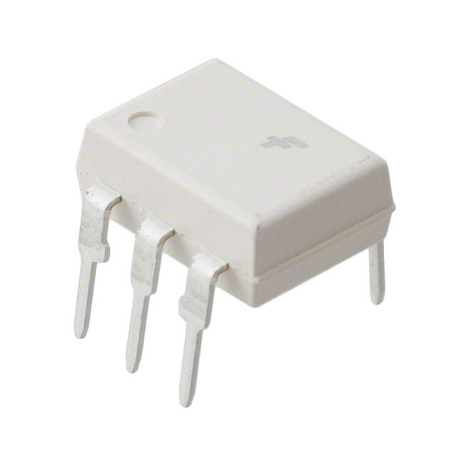
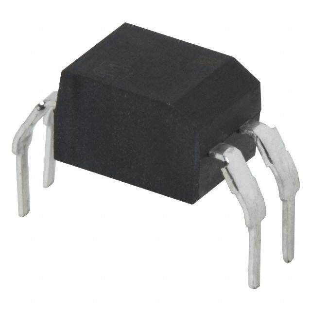
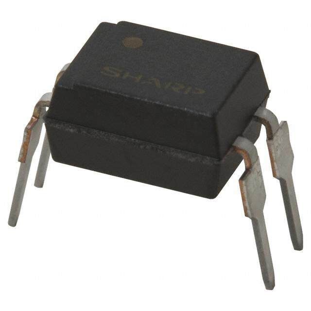
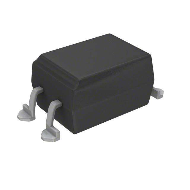
| 描述 | OPTOISO 7.5KV TRANS W/BASE 6DIP晶体管输出光电耦合器 Optocoupler Phototransistor |
| 产品分类 | |
| 品牌 | Fairchild Semiconductor |
| 产品手册 | |
| 产品图片 |
|
| rohs | 符合RoHS无铅 / 符合限制有害物质指令(RoHS)规范要求 |
| 产品系列 | 光耦合器/光电耦合器,晶体管输出光电耦合器,Fairchild Semiconductor 4N25VM- |
| 数据手册 | |
| 产品型号 | 4N25VM |
| Vce饱和值(最大值) | 500mV |
| 上升/下降时间(典型值) | - |
| 产品种类 | 晶体管输出光电耦合器 |
| 供应商器件封装 | 6-DIP |
| 包装 | 管件 |
| 单位重量 | 855 mg |
| 商标 | Fairchild Semiconductor |
| 安装类型 | 通孔 |
| 封装 | Bulk |
| 封装/外壳 | 6-DIP(0.300",7.62mm) |
| 封装/箱体 | PDIP-6 |
| 工作温度 | -40°C ~ 100°C |
| 工厂包装数量 | 1000 |
| 打开/关闭时间(典型值) | 2µs, 2µs |
| 最大功率耗散 | 150 mW |
| 最大反向二极管电压 | 6 V |
| 最大工作温度 | + 100 C |
| 最大正向二极管电压 | 1.5 V |
| 最大输入二极管电流 | 60 mA |
| 最大集电极/发射极电压 | 30 V |
| 最大集电极/发射极饱和电压 | 0.5 V |
| 最小工作温度 | - 40 C |
| 标准包装 | 1,000 |
| 每芯片的通道数量 | 1 Channel |
| 电压-正向(Vf)(典型值) | 1.18V |
| 电压-输出(最大值) | 30V |
| 电压-隔离 | 7500Vpk |
| 电流-DC正向(If) | 60mA |
| 电流-输出/通道 | - |
| 电流传输比(最大值) | - |
| 电流传输比(最小值) | 20% @ 10mA |
| 系列 | 4N25M |
| 绝缘电压 | 7500 Vrms |
| 输入类型 | DC |
| 输出类型 | DC |
| 输出设备 | NPN Phototransistor |
| 通道数 | 1 |
| 配置 | 1 Channel |
| 零件号别名 | 4N25VM_NL |
-angle.jpg)


.jpg)


- 商务部:美国ITC正式对集成电路等产品启动337调查
- 曝三星4nm工艺存在良率问题 高通将骁龙8 Gen1或转产台积电
- 太阳诱电将投资9.5亿元在常州建新厂生产MLCC 预计2023年完工
- 英特尔发布欧洲新工厂建设计划 深化IDM 2.0 战略
- 台积电先进制程称霸业界 有大客户加持明年业绩稳了
- 达到5530亿美元!SIA预计今年全球半导体销售额将创下新高
- 英特尔拟将自动驾驶子公司Mobileye上市 估值或超500亿美元
- 三星加码芯片和SET,合并消费电子和移动部门,撤换高东真等 CEO
- 三星电子宣布重大人事变动 还合并消费电子和移动部门
- 海关总署:前11个月进口集成电路产品价值2.52万亿元 增长14.8%
.jpg)


PDF Datasheet 数据手册内容提取
Is Now Part of To learn more about ON Semiconductor, please visit our website at www.onsemi.com Please note: As part of the Fairchild Semiconductor integration, some of the Fairchild orderable part numbers will need to change in order to meet ON Semiconductor’s system requirements. Since the ON Semiconductor product management systems do not have the ability to manage part nomenclature that utilizes an underscore (_), the underscore (_) in the Fairchild part numbers will be changed to a dash (-). This document may contain device numbers with an underscore (_). Please check the ON Semiconductor website to verify the updated device numbers. The most current and up-to-date ordering information can be found at www.onsemi.com. Please email any questions regarding the system integration to Fairchild_questions@onsemi.com. ON Semiconductor and the ON Semiconductor logo are trademarks of Semiconductor Components Industries, LLC dba ON Semiconductor or its subsidiaries in the United States and/or other countries. ON Semiconductor owns the rights to a number of patents, trademarks, copyrights, trade secrets, and other intellectual property. A listing of ON Semiconductor’s product/patent coverage may be accessed at www.onsemi.com/site/pdf/Patent-Marking.pdf. ON Semiconductor reserves the right to make changes without further notice to any products herein. ON Semiconductor makes no warranty, representation or guarantee regarding the suitability of its products for any particular purpose, nor does ON Semiconductor assume any liability arising out of the application or use of any product or circuit, and specifically disclaims any and all liability, including without limitation special, consequential or incidental damages. Buyer is responsible for its products and applications using ON Semiconductor products, including compliance with all laws, regulations and safety requirements or standards, regardless of any support or applications information provided by ON Semiconductor. “Typical” parameters which may be provided in ON Semiconductor data sheets and/or specifications can and do vary in different applications and actual performance may vary over time. All operating parameters, including “Typicals” must be validated for each customer application by customer’s technical experts. ON Semiconductor does not convey any license under its patent rights nor the rights of others. ON Semiconductor products are not designed, intended, or authorized for use as a critical component in life support systems or any FDA Class 3 medical devices or medical devices with a same or similar classification in a foreign jurisdiction or any devices intended for implantation in the human body. Should Buyer purchase or use ON Semiconductor products for any such unintended or unauthorized application, Buyer shall indemnify and hold ON Semiconductor and its officers, employees, subsidiaries, affiliates, and distributors harmless against all claims, costs, damages, and expenses, and reasonable attorney fees arising out of, directly or indirectly, any claim of personal injury or death associated with such unintended or unauthorized use, even if such claim alleges that ON Semiconductor was negligent regarding the design or manufacture of the part. ON Semiconductor is an Equal Opportunity/Affirmative Action Employer. This literature is subject to all applicable copyright laws and is not for resale in any manner.
4 N 2 5 April 2015 M , 4 N 2 6 M , 4 N 4N25M, 4N26M, 4N27M, 4N28M, 4N35M, 4N36M, 4N37M 2 7 6-Pin General Purpose Phototransistor Optocouplers M , 4 N 2 Features Description 8 M ■ Minimum Current Transfer Ratio at IF = 10 mA, The general purpose optocouplers consist of a gallium , 4 V = 10 V: arsenide infrared emitting diode driving a silicon photo- CE N – 10% for 4N27M and 4N28M transistor in a standard plastic six-pin dual-in-line 3 5 package. – 20% for 4N25M and 4N26M M – 100% for 4N35M, 4N36M and 4N37M , 4 N ■ Safety and Regulatory Approvals: 3 – UL1577, 4,170 VAC for 1 Minute 6 RMS M – DIN-EN/IEC60747-5-5, 850 V Peak Working , Insulation Voltage 4 N 3 Applications 7 M ■ Power Supply Regulators — ■ Digital Logic Inputs 6 ■ Microprocessor Inputs -P i n G e Schematic Package Outlines n e r a l 1 6 P u r p o 2 5 s e P h o 3 NC 4 t o t r a n s PIN 1. ANODE i s 2. CATHODE t o 3. NO CONNECTION r O 4. EMITTER Figure 2. Package Outlines p 5. COLLECTOR t o 6. BASE c o u Figure 1. Schematic p l e r s ©2005 Fairchild Semiconductor Corporation www.fairchildsemi.com 4N25M, 4N26M, 4N27M, 4N28M, 4N35M, 4N36M, 4N37M Rev. 1.3
4 N Safety and Insulation Ratings 2 5 M As per DIN EN/IEC 60747-5-5, this optocoupler is suitable for “safe electrical insulation” only within the safety limit , data. Compliance with the safety ratings shall be ensured by means of protective circuits. 4 N Parameter Characteristics 2 6 M Installation Classifications per DIN VDE < 150 VRMS I–IV , 0110/1.89 Table 1, For Rated Mains Voltage < 300 VRMS I–IV 4N 2 Climatic Classification 55/100/21 7 M Pollution Degree (DIN VDE 0110/1.89) 2 , 4 Comparative Tracking Index 175 N 2 8 M Symbol Parameter Value Unit , 4 N Input-to-Output Test Voltage, Method A, V x 1.6 = V , IORM PR 1360 V 3 Type and Sample Test with t = 10 s, Partial Discharge < 5 pC peak 5 V m M PR I1n0p0u%t-t oP-rOoduutpcutito Tne Tset sVto wltaithg et, M =e 1th so,d P Ba,r tViaIOl DRMis cxh 1a.r8g7e5 < = 5 V pPCR, 1594 Vpeak , 4 m N 3 V Maximum Working Insulation Voltage 850 V IORM peak 6 M V Highest Allowable Over-Voltage 6000 V IOTM peak , External Creepage ≥ 7 mm 4 N External Clearance ≥ 7 mm 3 7 M External Clearance (for Option TV, 0.4" Lead Spacing) ≥ 10 mm — DTI Distance Through Insulation (Insulation Thickness) ≥ 0.5 mm 6 T Case Temperature(1) 175 °C - S P IS,INPUT Input Current(1) 350 mA in P Output Power(1) 800 mW G S,OUTPUT e R Insulation Resistance at T , V = 500 V(1) > 109 Ω n IO S IO e r Note: a l 1. Safety limit values – maximum values allowed in the event of a failure. P u r p o s e P h o t o t r a n s i s t o r O p t o c o u p l e r s ©2005 Fairchild Semiconductor Corporation www.fairchildsemi.com 4N25M, 4N26M, 4N27M, 4N28M, 4N35M, 4N36M, 4N37M Rev. 1.3 2
4 N Absolute Maximum Ratings 2 5 M Stresses exceeding the absolute maximum ratings may damage the device. The device may not function or be , operable above the recommended operating conditions and stressing the parts to these levels is not recommended. 4 N In addition, extended exposure to stresses above the recommended operating conditions may affect device reliability. 2 The absolute maximum ratings are stress ratings only. T = 25°C unless otherwise specified. 6 A M Symbol Parameter Value Unit , 4 N TOTAL DEVICE 2 7 TSTG Storage Temperature -40 to +125 °C M T Operating Temperature -40 to +100 °C , OPR 4 N T Junction Temperature -40 to +125 ºC J 2 8 TSOL Lead Solder Temperature 260 for 10 seconds °C M Total Device Power Dissipation @ T = 25°C 270 mW , A 4 PD N Derate Above 25°C 2.94 mW/°C 3 5 EMITTER M I DC/Average Forward Input Current 60 mA , F 4 N V Reverse Input Voltage 6 V R 3 6 IF(pk) Forward Current – Peak (300 µs, 2% Duty Cycle) 3 A M LED Power Dissipation @ T = 25°C 120 mW , A 4 PD N Derate Above 25°C 1.41 mW/°C 3 7 DETECTOR M V Collector-to-Emitter Voltage 30 V — CEO VCBO Collector-to-Base Voltage 70 V 6 - P V Emitter-to-Collector Voltage 7 V ECO i n Detector Power Dissipation @ T = 25°C 150 mW A G P D Derate Above 25°C 1.76 mW/°C e n e r a l P u r p o s e P h o t o t r a n s i s t o r O p t o c o u p l e r s ©2005 Fairchild Semiconductor Corporation www.fairchildsemi.com 4N25M, 4N26M, 4N27M, 4N28M, 4N35M, 4N36M, 4N37M Rev. 1.3 3
4 N Electrical Characteristics 2 5 M TA = 25°C unless otherwise specified. , 4 Individual Component Characteristics N 2 Symbol Parameter Test Conditions Min. Typ. Max. Unit 6 M EMITTER , 4 V Input Forward Voltage I = 10 mA 1.18 1.50 V N F F 2 I Reverse Leakage Current V = 6.0 V 0.001 10 µA 7 R R M DETECTOR , 4 BV Collector-to-Emitter Breakdown Voltage I = 1.0 mA, I = 0 30 100 V N CEO C F 2 BV Collector-to-Base Breakdown Voltage I = 100 µA, I = 0 70 120 V 8 CBO C F M BVECO Emitter-to-Collector Breakdown Voltage IE = 100 µA, IF = 0 7 10 V , 4 I Collector-to-Emitter Dark Current V = 10 V, I = 0 1 50 nA N CEO CE F 3 I Collector-to-Base Dark Current V = 10 V 20 nA 5 CBO CB M CCE Capacitance VCE = 0 V, f = 1 MHz 8 pF , 4 N Transfer Characteristics 3 6 M Symbol Parameter Test Conditions Device Min. Typ. Max. Unit , 4 DC CHARACTERISTICS N 3 4N35M, 4N36M, 100 % 7 4N37M M I = 10 mA, V = 10 V F CE 4N25M, 4N26M 20 % — 4N27M, 4N28M 10 % 6 Current Transfer Ratio, - CTR P Collector-to-Emitter IF = 10 mA, VCE = 10 V, 4N35M, 4N36M, 40 % in TA = -55°C 4N37M G e IF = 10 mA, VCE = 10 V, 4N35M, 4N36M, n 40 % e T = +100°C 4N37M A r a 4N25M, 4N26M, l Collector-to-Emitter IC = 2 mA, IF = 50 mA 4N27M, 4N28M 0.5 V Pu VCE (SAT) Saturation Voltage 4N35M, 4N36M, rp IC = 0.5 mA, IF = 10 mA 4N37M 0.3 V os e AC CHARACTERISTICS P IF = 10 mA, VCC = 10 V, 4N25M, 4N26M, 2 µs ho R = 100 Ω (Figure 13) 4N27M, 4N28M t Non-Saturated L o TON Turn-on Time IC = 2 mA, VCC = 10 V, 4N35M, 4N36M, tra R = 100 Ω (Figure 13) 4N37M 2 10 µs n L s i IF = 10 mA, VCC = 10 V, 4N25M, 4N26M, st RL = 100 Ω (Figure 13) 4N27M, 4N28M 2 µs or TOFF Turn-off Time O IC = 2 mA, VCC = 10 V, 4N35M, 4N36M, p 2 10 µs RL = 100 Ω (Figure 13) 4N37M to c o Isolation Characteristics u p Symbol Characteristic Test Conditions Min. Typ. Max. Unit le r s V Input-Output Isolation Voltage t = 1 Minute 4170 VAC ISO RMS C Isolation Capacitance V = 0 V, f = 1 MHz 0.2 pF ISO I-O R Isolation Resistance V = ±500 VDC, T = 25°C 1011 Ω ISO I-O A ©2005 Fairchild Semiconductor Corporation www.fairchildsemi.com 4N25M, 4N26M, 4N27M, 4N28M, 4N35M, 4N36M, 4N37M Rev. 1.3 4
4 N Typical Performance Curves 2 5 M 1.8 1.6 , 4 1.7 1.4 VTAC E= =2 55°.0C V NIFo =rm 1a0l imzeAd to N2 6 LTAGE (V) 11..56 RTC 11..02 M, 4N VO D 2 V - FORWARD F 111...234 TTAA == 2-555°°CC EZILAMRON 000...468 7M, 4N2 8 TA = 100°C M 1.1 0.2 , 4 1.0 0.0 N 1 10 100 0 2 4 6 8 10 12 14 16 18 20 3 IF - LED FORWARD CURRENT (mA) IF - FORWARD CURRENT (mA) 5 M Figure 3. LED Forward Voltage vs. Forward Current Figure 4. Normalized CTR vs. Forward Current , 4 N 3 6 1.4 1.0 M 1.2 )E(OPEN) 00..89 IF = 20 mA , 4N RTC DE 1.0 IF = 10 mAI F = 5 mA R / CTRRBERB 000...567 IF = 10 mA IF = 5 mA 37M — ZIL 0.8 CT 6 AM R ( 0.4 -P RON 0.6 IF = 20 mA D CT 0.3 in ZE 0.2 G 0.4 MALI 0.1 VCE = 5.0 V en NITFAo = r=m 1 2a05l im°zCeAd to NOR 0.0 era 0.2 l -60 -40 -20 0 20 40 60 80 100 10 100 1000 P TA - AMBIENT TEMPERATURE (°C) RBE- BASE RESISTANCE (kΩ) u r Figure 5. Normalized CTR vs. Ambient Temperature Figure 6. CTR vs. RBE (Unsaturated) p o s e 1.0 100 P )EN) 0.9 ho / CTRBERBE(OP 000...678 IF = 20 mA VCE= 0.3 V TOR-EMITTER OLTAGE (V) 110 TA = 25˚C totransi ALIZED CTR ( CTRR 0000....2345 IF I=F 1 =0 5m mAA V - COLLECCE (SAT)SATURATION V00.0.11 IF = 2.5 mA IF = 20 mA stor Optoc M o OR 0.1 u N 0.0 0.001 IF = 5 mA IF = 10 mA pl 10 100 1000 0.01 0.1 1 10 e RBE- BASE RESISTANCE (kΩ) IC - COLLECTOR CURRENT (mA) rs Figure 7. CTR vs. RBE (Saturated) Figure 8. Collector-Emitter Saturation Voltage vs. Collector Current ©2005 Fairchild Semiconductor Corporation www.fairchildsemi.com 4N25M, 4N26M, 4N27M, 4N28M, 4N35M, 4N36M, 4N37M Rev. 1.3 5
4 N Typical Performance Curves (Continued) 2 5 M μ)s( - DEEPS GNIHCTIWS1101001000 IVTFAC = C= 1 =20 51 m°0C AV Toff TTorn Tf )t / t( - t DEZILAMR)nepo(no)R(nonoEB 12233445........50505050 VIRCCL = C= 2 =1 m0100A VΩ , 4N26M, 4N27M, 4N2 O 8 N 1.0 M 0.1 0.5 , 4 0.1 1 10 100 10 100 1000 10000 100000 N R - LOAD RESISTOR (kΩ) RBE - BASE RESISTANCE (kΩ) 3 5 Figure 9. Switching Speed vs. Load Resistor Figure 10. Normalized ton vs. RBE M , 4 N 3 1.4 )A 10000 6 )t / t( - t DEZILAMRON)nepo(ffo)R(ffoffoEB 00000001111...........34567890123 VIRCCL = C= 2 =1 m0100A VΩ n( TNERRUC KRAD RETTIME- ROTCELLOC - OE 10100.1000.000111 VTAC E= =2 51°0C V M, 4N37M — 6-Pin Ge 0.2 IC n 0.1 0.001 e 10 100 1000 10000 100000 0 20 40 60 80 100 ra RBE - BASE RESISTANCE (kΩ) TA - AMBIENT TEMPERATURE (°C) l P Figure 11. Normalized toff vs. RBE Figure 12. Dark Current vs. Ambient Temperature u r p o s e Switching Time Test Circuit and Waveforms P h o t o TEST CIRCUIT WAVE FORMS t r a n VCC = 10 V si s INPUT PULSE t o IF IC RL r O 10% p INPUT OUTPUT OUTPUT PULSE to 90% c RBE o tr tf u p ton toff le Adjust IF to produce IC = 2 mA r s Figure 13. Switching Time Test Circuit and Waveforms ©2005 Fairchild Semiconductor Corporation www.fairchildsemi.com 4N25M, 4N26M, 4N27M, 4N28M, 4N35M, 4N36M, 4N37M Rev. 1.3 6
4 N Reflow Profile 2 5 M 300 , 4 260°C N 280 2 6 260 M 240 > 245°C = 42 s , 4 N 220 2 7 200 M 180 , Time above 4 N °C 160 183°C = 90 s 2 8 140 M 120 , 4 100 1.822°C/s Ramp-up rate N 3 5 80 M 60 , 4 N 40 3 20 33 s 6 M 0 , 0 60 120 180 270 360 4 N Time (s) 3 7 M Figure 14. Reflow Profile — 6 - P i n G e n e r a l P u r p o s e P h o t o t r a n s i s t o r O p t o c o u p l e r s ©2005 Fairchild Semiconductor Corporation www.fairchildsemi.com 4N25M, 4N26M, 4N27M, 4N28M, 4N35M, 4N36M, 4N37M Rev. 1.3 7
4 N Ordering Information 2 5 M Part Number Package Packing Method , 4 N 4N25M DIP 6-Pin Tube (50 Units) 2 6 4N25SM SMT 6-Pin (Lead Bend) Tube (50 Units) M 4N25SR2M SMT 6-Pin (Lead Bend) Tape and Reel (1000 Units) , 4 N 4N25VM DIP 6-Pin, DIN EN/IEC60747-5-5 Option Tube (50 Units) 2 7 4N25SVM SMT 6-Pin (Lead Bend), DIN EN/IEC60747-5-5 Option Tube (50 Units) M 4N25SR2VM SMT 6-Pin (Lead Bend), DIN EN/IEC60747-5-5 Option Tape and Reel (1000 Units) , 4 N 4N25TVM DIP 6-Pin, 0.4” Lead Spacing, DIN EN/IEC60747-5-5 Option Tube (50 Units) 2 8 Note: M 2. The product orderable part number system listed in this table also applies to the 4N26M, 4N27M, 4N28M, 4N35M, , 4 4N36M, and 4N37M devices. N 3 5 M Marking Information , 4 N 3 6 M 1 , 4 N 4N25 2 3 7 M V X YY Q 6 — 6 - P i n 3 4 5 G e n Figure 15. Top Mark e r a Table 1. Top Mark Definitions l P u 1 Fairchild Logo r p 2 Device Number o s 3 DIN EN/IEC60747-5-5 Option (only appears on component ordered with this option) e P 4 One-Digit Year Code, e.g., “5” h o 5 Digit Work Week, Ranging from “01” to “53” t o 6 Assembly Package Code tr a n s i s t o r O p t o c o u p l e r s ©2005 Fairchild Semiconductor Corporation www.fairchildsemi.com 4N25M, 4N26M, 4N27M, 4N28M, 4N35M, 4N36M, 4N37M Rev. 1.3 8
None
None
None
ON Semiconductor and are trademarks of Semiconductor Components Industries, LLC dba ON Semiconductor or its subsidiaries in the United States and/or other countries. ON Semiconductor owns the rights to a number of patents, trademarks, copyrights, trade secrets, and other intellectual property. A listing of ON Semiconductor’s product/patent coverage may be accessed at www.onsemi.com/site/pdf/Patent−Marking.pdf. ON Semiconductor reserves the right to make changes without further notice to any products herein. ON Semiconductor makes no warranty, representation or guarantee regarding the suitability of its products for any particular purpose, nor does ON Semiconductor assume any liability arising out of the application or use of any product or circuit, and specifically disclaims any and all liability, including without limitation special, consequential or incidental damages. Buyer is responsible for its products and applications using ON Semiconductor products, including compliance with all laws, regulations and safety requirements or standards, regardless of any support or applications information provided by ON Semiconductor. “Typical” parameters which may be provided in ON Semiconductor data sheets and/or specifications can and do vary in different applications and actual performance may vary over time. All operating parameters, including “Typicals” must be validated for each customer application by customer’s technical experts. ON Semiconductor does not convey any license under its patent rights nor the rights of others. ON Semiconductor products are not designed, intended, or authorized for use as a critical component in life support systems or any FDA Class 3 medical devices or medical devices with a same or similar classification in a foreign jurisdiction or any devices intended for implantation in the human body. Should Buyer purchase or use ON Semiconductor products for any such unintended or unauthorized application, Buyer shall indemnify and hold ON Semiconductor and its officers, employees, subsidiaries, affiliates, and distributors harmless against all claims, costs, damages, and expenses, and reasonable attorney fees arising out of, directly or indirectly, any claim of personal injury or death associated with such unintended or unauthorized use, even if such claim alleges that ON Semiconductor was negligent regarding the design or manufacture of the part. ON Semiconductor is an Equal Opportunity/Affirmative Action Employer. This literature is subject to all applicable copyright laws and is not for resale in any manner. PUBLICATION ORDERING INFORMATION LITERATURE FULFILLMENT: N. American Technical Support: 800−282−9855 Toll Free ON Semiconductor Website: www.onsemi.com Literature Distribution Center for ON Semiconductor USA/Canada 19521 E. 32nd Pkwy, Aurora, Colorado 80011 USA Europe, Middle East and Africa Technical Support: Order Literature: http://www.onsemi.com/orderlit Phone: 303−675−2175 or 800−344−3860 Toll Free USA/Canada Phone: 421 33 790 2910 Fax: 303−675−2176 or 800−344−3867 Toll Free USA/Canada Japan Customer Focus Center For additional information, please contact your local Email: orderlit@onsemi.com Phone: 81−3−5817−1050 Sales Representative © Semiconductor Components Industries, LLC www.onsemi.com www.onsemi.com 1
Mouser Electronics Authorized Distributor Click to View Pricing, Inventory, Delivery & Lifecycle Information: O N Semiconductor: 4N25SR2M 4N25SR2VM 4N25VM 4N25M 4N25SVM 4N25TVM 4N25SM 4N25M_Q