ICGOO在线商城 > 射频/IF 和 RFID > RF 收发器模块 > 450-0104
 Datasheet下载
- 型号: 450-0104
- 制造商: LS Research
- 库位|库存: xxxx|xxxx
- 要求:
| 数量阶梯 | 香港交货 | 国内含税 |
| +xxxx | $xxxx | ¥xxxx |
查看当月历史价格
查看今年历史价格
450-0104产品简介:
ICGOO电子元器件商城为您提供450-0104由LS Research设计生产,在icgoo商城现货销售,并且可以通过原厂、代理商等渠道进行代购。 450-0104价格参考。LS Research450-0104封装/规格:RF 收发器模块, 。您可以下载450-0104参考资料、Datasheet数据手册功能说明书,资料中有450-0104 详细功能的应用电路图电压和使用方法及教程。
Laird - Wireless & Thermal Systems 的450-0104型号RF收发器模块是一款高性能的射频通信设备,适用于多种应用场景。以下是其主要应用场景:

 1. 工业自动化
   在工业环境中,450-0104模块可以用于实现机器与机器之间的无线通信(M2M),支持工厂自动化系统中的数据传输。它能够在复杂的电磁环境下稳定工作,确保生产线上的传感器、控制器和执行器之间的实时通信,提高生产效率和可靠性。

 2. 智能电网
   该模块可用于智能电表和其他电力设备之间的数据传输,帮助电力公司实时监控电网状态,优化能源分配。通过无线通信,它可以将用电量、电压、电流等信息传输到中央控制系统,支持远程抄表和故障诊断。

 3. 智能家居
   在智能家居系统中,450-0104模块可以作为无线通信的核心组件,连接各种智能设备,如温控器、安防摄像头、门锁等。它能够提供稳定的射频信号,确保家庭内部设备之间的无缝通信,提升用户的智能化体验。

 4. 物流与仓储管理
   在物流和仓储管理系统中,该模块可以用于资产追踪和库存管理。通过安装在货物或设备上的标签,结合RFID技术,450-0104模块能够实现实时位置跟踪和数据上传,帮助企业提高库存管理的精度和效率。

 5. 医疗设备
   在医疗领域,该模块可用于远程医疗设备的数据传输,如心率监测仪、血糖仪等。它能够将患者的生理数据实时传输到医生的终端设备,支持远程诊断和健康监测,特别适用于慢性病患者的家庭护理。

 6. 环境监测
   450-0104模块还可以应用于环境监测系统,如空气质量监测站、水质检测设备等。它能够将传感器采集的数据传输到数据中心,帮助环保部门实时掌握环境变化,及时采取应对措施。

总之,Laird 450-0104 RF收发器模块凭借其高可靠性和低功耗特性,广泛应用于工业、能源、家居、物流、医疗和环保等多个领域,满足不同场景下的无线通信需求。
| 参数 | 数值 |
| 产品目录 | |
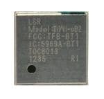
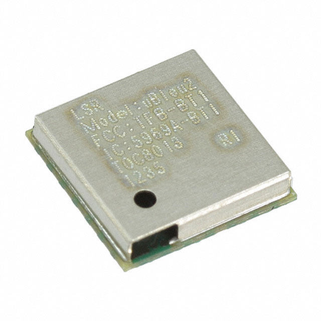
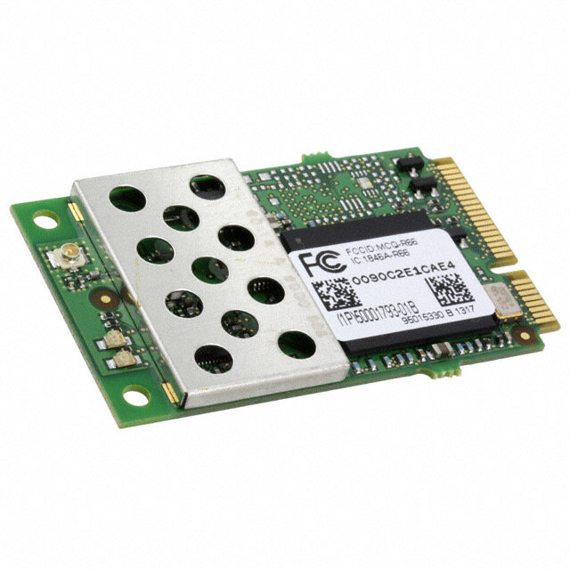
| 描述 | BLUETOOTH MODULE TIWI-UB2蓝牙/802.15.1 模块 TiWi-uB2 Module,Tray BT 2.1+ EDR, BLE 4.0 |
| 产品分类 | RF 收发器射频/无线模块 |
| 品牌 | LS Research |
| 产品手册 | |
| 产品图片 |
|
| rohs | 符合RoHS无铅 / 符合限制有害物质指令(RoHS)规范要求 |
| 产品系列 | 蓝牙/802.15.1 模块,LS Research 450-0104- |
| 数据手册 | |
| 产品型号 | 450-0104 |
| RoHS指令信息 | |
| Version | 4.0 |
| 产品种类 | 蓝牙/802.15.1 模块 |
| 其它名称 | 4500104 |
| 功率-输出 | 10dBm |
| 包装 | 托盘 |
| 商标 | LS Research |
| 型号 | 4.0 |
| 天线连接器 | PCB,表面贴装 |
| 天线连接器类型 | Chip, Dipole |
| 存储容量 | - |
| 安装风格 | SMD/SMT |
| 封装/外壳 | 模块 |
| 尺寸 | 7 mm x 7 mm x 1.5 mm |
| 工作温度 | -30°C ~ 85°C |
| 工作电源电压 | 2.2 V to 4.8 V |
| 工厂包装数量 | 416 |
| 应用 | 通用 |
| 接口类型 | HCI UART |
| 数据接口 | PCB,表面贴装 |
| 数据速率 | 4000 kb/s |
| 数据速率(最大值) | - |
| 最大工作温度 | + 85 C |
| 最小工作温度 | - 30 C |
| 标准包装 | 416 |
| 灵敏度 | - 94 dB |
| 电压-电源 | 2.2 V ~ 4.8 V |
| 电流-传输 | 47.1mA |
| 电流-接收 | 38.8mA |
| 类 | 1.5 |
| 调制或协议 | 蓝牙 v4.0,低功耗 |
| 调制技术 | FHSS, GFSK, DPSK, DQPSK |
| 输出功率 | 10 dBm |
| 配用 | /product-detail/zh/450-0105/450-0105-ND/3661881 |
| 频带 | 2.4 GHz |
| 频率 | 2.4GHz |


- 商务部:美国ITC正式对集成电路等产品启动337调查
- 曝三星4nm工艺存在良率问题 高通将骁龙8 Gen1或转产台积电
- 太阳诱电将投资9.5亿元在常州建新厂生产MLCC 预计2023年完工
- 英特尔发布欧洲新工厂建设计划 深化IDM 2.0 战略
- 台积电先进制程称霸业界 有大客户加持明年业绩稳了
- 达到5530亿美元!SIA预计今年全球半导体销售额将创下新高
- 英特尔拟将自动驾驶子公司Mobileye上市 估值或超500亿美元
- 三星加码芯片和SET,合并消费电子和移动部门,撤换高东真等 CEO
- 三星电子宣布重大人事变动 还合并消费电子和移动部门
- 海关总署:前11个月进口集成电路产品价值2.52万亿元 增长14.8%


PDF Datasheet 数据手册内容提取
TiWi-uB2 Module DATASHEET TiWi-uB2 Bluetooth Module FEATURES DESCRIPTION • Built in CC2564 single-chip Bluetooth fully LSR would like to announce a low-cost and low- supports BT 2.1 + EDR, BLE 4.0. power consumption module which has all of the • RF Output Power: +10 dBm (Class 1.5) Bluetooth functionalities. The highly integrated TiWi-uB2 module makes the use of Bluetooth • RF Receive Sensitivity: -94 dBm headsets and other applications possible. • Miniature Size: 7 mm x 7 mm x 1.5 mm • Operating Voltage: 2.2V to 4.8V • Operating temperature: -30 to +85o C • Worldwide acceptance: FCC (USA), IC (Canada), ETSI (Europe), Giteki (Japan) • RoHS compliant • Supports maximum Bluetooth data rates over HCI UART interface. • Supports multiple Bluetooth profiles with The TiWi-uB2 module fully supports the dual mode enhanced QoS, both mono and stereo, Bluetooth and BLE operation, and the output power assisted A2DP can support class 1.5. The SIP module provides UART interface / audio PCM interface for Bluetooth. APPLICATIONS The SIP module is specifically developed for Smart • Medical (ex Heart Rate Monitor, Blood phones and Portable devices. Pressure Sensor, Blood Glucose Meter) Need to get to market quickly? Not an expert in • Thermometer Bluetooth? Need a custom antenna? Do you need • Flood Alarm help with your host board? LSR Design Services will • Heating Control be happy to develop custom hardware or software, • Automatic Key Control or help integrate the design. Contact us at • Industrial Sensors sales@lsr.com or call us at 262-375-4400. • Toys • Entertainment Devices • Mobile Accessories • All Bluetooth Wireless Applications ORDERING INFORMATION Order Number Description 450-0104 TiWi-uB2 Module (Tray) 450-0104R TiWi-uB2 Module (Tape & Reel) 450-0105 TiWi-uB2 EM Board Table 1 Orderable Model Numbers The information in this document is subject to change without notice. 330-0100-R1.5 Copyright © 2012-2018 LSR Page 1 of 36
TiWi-uB2 Module DATASHEET MODULE ACCESSORIES Order Number Description 2.4 GHz Dipole Antenna with Reverse Polarity 001-0001 SMA Connector U.FL to Reverse Polarity SMA Bulkhead Cable 080-0001 105mm Table 2 Module Accessories The information in this document is subject to change without notice. 330-0100-R1.5 Copyright © 2012-2018 LSR Page 2 of 36
TiWi-uB2 Module DATASHEET BLOCK DIAGRAM Figure 1 TiWi-uB2 Module Block Diagram The information in this document is subject to change without notice. 330-0100-R1.5 Copyright © 2012-2018 LSR Page 3 of 36
TiWi-uB2 Module DATASHEET TABLE OF CONTENTS FEATURES ................................................................................................................................... 1 APPLICATIONS ............................................................................................................................ 1 DESCRIPTION .............................................................................................................................. 1 ORDERING INFORMATION .......................................................................................................... 1 MODULE ACCESSORIES ................................................................................................................ 2 BLOCK DIAGRAM ........................................................................................................................ 3 FOOTPRINT AND PIN DEFINITIONS .............................................................................................. 6 PIN DESCRIPTIONS ...................................................................................................................... 8 ELECTRICAL SPECIFICATIONS ....................................................................................................... 9 Absolute Maximum Ratings ................................................................................................................................... 9 Recommended Operating Conditions .................................................................................................................... 9 General Characteristics ........................................................................................................................................ 10 Current Consumption for Active and Standby States ........................................................................................... 10 Bluetooth RF Characteristics ................................................................................................................................ 13 BLUETOOTH POWER-UP/ DOWN SEQUENCE ............................................................................. 15 nSHUTD Requirements ........................................................................................................................................ 15 SLOW CLOCK (32 KHZ) SOURCE REQUIREMENTS ........................................................................ 18 BLUETOOTH HCI UART .............................................................................................................. 19 BLUETOOTH AUDIO CODEC/PCM .............................................................................................. 20 SOLDERING RECOMMENDATIONS ............................................................................................. 21 Recommended Reflow Profile for Lead Free Solder ............................................................................................. 21 CLEANING ................................................................................................................................. 22 OPTICAL INSPECTION ................................................................................................................ 22 REWORK ................................................................................................................................... 22 SHIPPING, HANDLING, AND STORAGE ....................................................................................... 22 Shipping ............................................................................................................................................................... 22 The information in this document is subject to change without notice. 330-0100-R1.5 Copyright © 2012-2018 LSR Page 4 of 36
TiWi-uB2 Module DATASHEET Handling .............................................................................................................................................................. 22 Moisture Sensitivity Level (MSL) .......................................................................................................................... 22 Storage ................................................................................................................................................................ 22 Repeating Reflow Soldering ................................................................................................................................. 23 AGENCY CERTIFICATIONS .......................................................................................................... 24 AGENCY STATEMENTS ............................................................................................................... 24 Federal Communication Commission Interference Statement ............................................................................. 24 Industry Canada Statements ................................................................................................................................ 25 OEM RESPONSIBILITIES TO COMPLY WITH FCC AND INDUSTRY CANADA REGULATIONS ............. 26 OEM LABELING REQUIREMENTS FOR END-PRODUCT ................................................................. 27 OEM END PRODUCT USER MANUAL STATEMENTS ..................................................................... 28 EUROPE .................................................................................................................................... 29 CE Notice ............................................................................................................................................................. 29 Declaration of Conformity (DOC) ......................................................................................................................... 29 BLUETOOTH CERTIFICATION ...................................................................................................... 29 MECHANICAL DATA ................................................................................................................... 30 Tape & Reel Dimensions ...................................................................................................................................... 32 Tray Dimensions .................................................................................................................................................. 33 DEVICE MARKINGS .................................................................................................................... 34 Rev 1 Devices ....................................................................................................................................................... 34 Rev 2 Devices ....................................................................................................................................................... 34 Rev 3 Devices ....................................................................................................................................................... 35 CONTACTING LSR ...................................................................................................................... 36 The information in this document is subject to change without notice. 330-0100-R1.5 Copyright © 2012-2018 LSR Page 5 of 36
TiWi-uB2 Module DATASHEET FOOTPRINT AND PIN DEFINITIONS Figure 2 TiWi-uB2 Module Schematic View The information in this document is subject to change without notice. 330-0100-R1.5 Copyright © 2012-2018 LSR Page 6 of 36
TiWi-uB2 Module DATASHEET Figure 3 TiWi-uB2 Module Footprint View The information in this document is subject to change without notice. 330-0100-R1.5 Copyright © 2012-2018 LSR Page 7 of 36
TiWi-uB2 Module DATASHEET PIN DESCRIPTIONS Module Name I/O Type Description Pin 1 HCI_CTS I HCI UART CLEAR-TO-SEND 2 HCI_TX O HCI UART DATA TRANSMIT 3 HCI_RX I HCI UART DATA RECEIVE 4 HCI_RTS O HCI UART REQUEST-TO-SEND 5 GND GND GROUND 6 GND GND GROUND 7 GND GND GROUND 8 SLOW_CLK_IN I 32.768 kHz CLOCK IN 9 GND GND GROUND 10 NC1 O NO CONNECT 1 (DO NOT CONNECT) 11 NC2 O NO CONNECT 2 (DO NOT CONNECT) 12 VBAT PI POWER TO MODULE (2.2V - 4.8V) 13 GND GND GROUND 14 BT_ANT RF ANTENNA, 50 OHMS 15 GND GND GROUND 16 nSHUTD I SHUTDOWN INPUT (ACTIVE LOW) 17 GND GND GROUND 18 VDD_IO PI I/O POWER SUPPLY (1.8V NOMINAL) 19 AUD_IN I PCM DATA INPUT (IF NOT USED, DO NOT CONNECT) 20 AUD_OUT O PCM DATA OUTPUT (IF NOT USED, DO NOT CONNECT) 21 AUD_CLK IO PCM CLOCK (IF NOT USED, DO NOT CONNECT) 22 AUD_FSYNC IO PCM FRAME SYNCH (IF NOT USED, DO NOT CONNECT) 23 NC3 O NO CONNECT 3 (DO NOT CONNECT) 24 TX_DBG O LOGGER OUTPUT 25-33 GND GND GROUND PI = Power Input I = Input O = Output IO = Bi-directional Input Output Port RF = Bi-directional RF Port GND=Ground Table 3 TiWi-uB2 Pin Descriptions The information in this document is subject to change without notice. 330-0100-R1.5 Copyright © 2012-2018 LSR Page 8 of 36
TiWi-uB2 Module DATASHEET ELECTRICAL SPECIFICATIONS Absolute Maximum Ratings Symbol Description Min Max Unit VBAT Input supply Voltage -0.5 5.5 V VDD_IO Digital Bluetooth I/O Voltage -0.5 2.145 V Table 4 Absolute Maximum Ratings1 Recommended Operating Conditions Test conditions: Ambient Temp = 25°C Symbol Min Typ Max Unit VBAT 2.2 3.3 4.8 V VDD_IO 1.62 1.8 1.92 V Table 5 Recommended Operating Conditions 1 Under no circumstances should exceeding the ratings specified in the Absolute Maximum Ratings section be allowed. Stressing the module beyond these limits may result permanent damage to the module that is not covered by the warranty. The information in this document is subject to change without notice. 330-0100-R1.5 Copyright © 2012-2018 LSR Page 9 of 36
TiWi-uB2 Module DATASHEET General Characteristics Characteristic Description Model Name TiWi-uB2 Product Description Bluetooth Wireless Module Dimension 7.0 mm x 7.0 mm x 1.5 mm (W*L*T) BT Interface HCI UART, Audio PCM Operating temperature -30°C to 85°C Storage temperature -40°C to 85°C Operating Humidity 10% to 95% Non-Condensing Humidity Storage Humidity 5% to 95% Non-Condensing Weight 0.18 g +/- 0.01g Table 6 General Characteristics Current Consumption for Active and Standby States Min Typ Max Min Min Typ Max Min Typ Max Mode Description Unit 25°C 25°C 25°C -40°C -40°C -40°C -40°C 85°C 85°C 85°C Current consumption in shut- 1 3 7 µA down mode(1) Current consumption in deep- 40 105 µA sleep mode(2) Total I/O current consumption 1 1 1 µA for active mode Table 7 Current Consumption for Active and Standby States (1) Vbat + Vio (2) Vbat + Vio + Vsd (shutdown) The information in this document is subject to change without notice. 330-0100-R1.5 Copyright © 2012-2018 LSR Page 10 of 36
TiWi-uB2 Module DATASHEET Current Consumption – for Different Bluetooth BR/EDR Scenarios Conditions: VBAT = 3.6 V, VDD_IO = 1.8V, 25°C, 26 MHz fast clock, nominal unit, 4 dBm output power Mode Description Master/Slave Average Current Unit Idle current (ARM off) Master/slave 2.5 mA SCO link HV3 Master/slave 12 mA eSCO link EV3 64 kbps, no retransmission Master/slave 11.5 mA eSCO link 2-EV3 64 kbps, no retransmission Master/slave 8.3 mA GFSK full throughput: TX = DH1, RX = DH5 Master/slave 38.5 mA EDR full throughput: TX = 2-DH1, RX = 2-DH5 Master/slave 39.2 mA EDR full throughput: TX = 3-DH1, RX = 3-DH5 Master/slave 39.2 mA Sniff, one attempt, 1.28 s Master/slave 76/100 µA Page or inquiry scan 1.28 s, 11.25 ms Master/slave 300 µA Page (1.28 s) and inquiry (2.56 s) scans, 11.25 ms Master/slave 430 µA Low power scan, 1.28-s interval, quiet environment Master/slave 135 µA Table 8 Bluetooth Power Consumption The information in this document is subject to change without notice. 330-0100-R1.5 Copyright © 2012-2018 LSR Page 11 of 36
TiWi-uB2 Module DATASHEET Current Consumption – for Different Bluetooth LE Scenarios Conditions: VBAT = 3.6 V, VDD_IO = 1.8V, 25°C, 26 MHz fast clock, nominal unit, 10 dBm output power Mode Description Average Current Unit Advertising in all 3 channels Advertising, non- 1.28msec advertising interval 104 µA connectable 15Bytes advertise data Advertising in all 3 channels Advertising, discoverable 1.28msec advertising interval 121 µA 15Bytes advertise data Listening to a single frequency per window Scanning 1.28msec scan interval 302 µA 11.25msec scan window 500msec connection interval Connected (master role) 0msec Slave connection latency 169 µA Empty Tx/Rx LL packets Table 9 Bluetooth Power Consumption Power Consumption – Bluetooth Conditions: VBAT = 3.3V, VDD_IO = 1.8V, Ambient Temp = 25°C Packet type Typ Max Unit DM1 47.1 mA DH1 30.2 mA DM3 21.3 mA DH3 17.4 mA DM5 15.6 mA DH5 13.0 mA Deep Sleep Mode 0.033 mA Constant RX 44.5 mA BER Mode 38.8 mA Table 10 Bluetooth VBAT Power Consumption The information in this document is subject to change without notice. 330-0100-R1.5 Copyright © 2012-2018 LSR Page 12 of 36
TiWi-uB2 Module DATASHEET Packet type Typ Max Unit DM1 0.069 mA DH1 0.069 mA DM3 0.069 mA DH3 0.069 mA DM5 0.069 mA DH5 0.069 mA Deep Sleep mode 0.032 mA Constant RX 0.069 mA BER Mode 0.069 mA Table 11 Bluetooth VDDIO Power Consumption Bluetooth RF Characteristics General Specifications Feature Description Bluetooth Standard Bluetooth 4.0 (with EDR) Host Interface HCI UART, PCM Antenna Reference Small antennas with 0~2 dBi peak gain Frequency Band 2.402 GHz ~ 2.480 GHz Number of Channels 79 channels Modulation FHSS, GFSK, DPSK, DQPSK Table 12 Bluetooth General Specifications The information in this document is subject to change without notice. 330-0100-R1.5 Copyright © 2012-2018 LSR Page 13 of 36
TiWi-uB2 Module DATASHEET RF Characteristics Test Conditions : VBAT = 3.3V, VDD_IO = 1.8V Characteristic Condition -30°C Typ 25°C Typ 85°C Typ BT Spec Unit Output Power Class 1.5 9.5 10 10.8 dBm dF1 avg 158 158 158 140~ 175 KHz Modulation dF2 max 138 137 136 >115 KHz GFSK dF2 / dF1 90 90 90 80 % avg avg RMS DEVM 5 5 5 13 % Modulation 99% DEVM 10 10 10 20 % EDR at 8DPSK Peak DEVM 13 13 13 25 % GFSK at BER = 0.1% -95 -94 -93 -70 dBm Sensitivity at π/4-DQPSK at BER = 0.01% -93 -92 -91 -70 dBm Dirty Tx On 8DPSK at BER = 0.01% -86 -85 -84 -70 dBm GFSK at BER = 0.1% -5 -5 -5 -20 dBm Maximum π/4-DQPSK at BER = 0.1% -10 -10 -10 -20 dBm Input Level 8DPSK at BER = 0.1% -10 -10 -10 -20 dBm Table 13 Bluetooth RF Characteristics The information in this document is subject to change without notice. 330-0100-R1.5 Copyright © 2012-2018 LSR Page 14 of 36
TiWi-uB2 Module DATASHEET BLUETOOTH POWER-UP/ DOWN SEQUENCE Power up requirements: • nSHUTD must be low. VDD_IN and VDD_IO are don't-care when nSHUTD is low. However, no signals are allowed on the I/O pins if no I/O power is supplied, because the I/Os are not fail-safe. Exceptions are SLOW_CLK_IN, XTALP, XTALM, and AUD_xxx, which are fail-safe and can tolerate external voltages with no VDD_IO and VDD_IN. • VDD_IO and VDD_IN must be stable before releasing nSHUTD. • Fast clock must be stable maximum 20 ms after nSHUTD goes high. • Slow clock must be stable within 2 ms of nSHUTD going high. The CC256x indicates that the power-up sequence is complete by asserting RTS low. This occurs up to100 ms after nSHUTD goes high. Figure 4 Bluetooth Power-Up/Down Sequence nSHUTD Requirements Parameter Symbol Min Max Unit Operation mode level (1) V 1.42 1.98 V IH Shutdown mode level (1) V 0 0.4 V IL Minimum time for nSHUT_DOWN low to reset the device 5 Rise/fall times Tr/Tf 20 us (1) Internal pull-down retains shutdown mode when no external signal is applied to this pin. Table 14 nSHUTD Requirements The information in this document is subject to change without notice. 330-0100-R1.5 Copyright © 2012-2018 LSR Page 15 of 36
TiWi-uB2 Module DATASHEET Power Supplies and Shutdown—Static States The nSHUTD signal puts the CC256x in ultra-low power mode and also performs an internal reset to the device. nSHUTD rise time must not exceed 20 μs, and nSHUTD must be low for a minimum of 5 ms. All I/O pins are set to high-impedance state during shut down and power up of the CC256x device to prevent conflicts with external signals. The internal pull resistors are enabled on each I/O pin. VDD_IN(1) VDD_IO(1) nSHUTD(1) PM_MODE Comments I/O state is undefined. No I/O voltages allowed on non 1 None None Asserted Shut Down fail-safe pins. I/O state is undefined. No I/O voltages allowed on non 2 None None Deasserted Not Allowed fail-safe pins. IOs are defined as 3-state with internal pullup/pulldown 3 None Present Asserted Shut Down enabled. I/O state is undefined. No I/O voltages allowed on non 4 None Present Deasserted Not Allowed fail-safe pins. I/O state is undefined. No I/O voltages allowed on non 5 Present None Asserted Shut Down fail-safe pins. I/O state is undefined. No I/O voltages allowed on non 6 Present None Deasserted Not Allowed fail-safe pins. IOs are defined as 3-state with internal pullup/pulldown 7 Present Present Asserted Shut Down enabled. 8 Present Present Deasserted Active See Table 16 I/O States in Various Power Modes Table 15 Power Modes (1) None/Asserted can be any of the following conditions: directly pulled to ground/driven low, pulled to ground through pull down resistor, or left NC/floating (high-impedance output stage). The information in this document is subject to change without notice. 330-0100-R1.5 Copyright © 2012-2018 LSR Page 16 of 36
TiWi-uB2 Module DATASHEET I/O Name Shut Down Default Active (1) Deep Sleep (2) I/O State Pull I/O State Pull I/O State Pull HCI_RX Z PU I PU I (3) HCI_TX Z PU O-H - O - HCI_RTS Z PU O-H - O - HCI_CTS Z PU I PU I (3) AUD_CLK Z PD I PD I PD AUD_FSYNC Z PD I PD I PD AUD_IN Z PD I PD I PD AUD_OUT Z PD Z PD Z PD I2C_SCL Z (4) I (4) I (4) I2C_SDA Z (4) I (4) I (4) TX_DBG Z PU O - Table 16 I/O States in Various Power Modes (1) I = input, O = output, Z = HiZ, — = no pull (2) Shown only if different from active. Can be changed by vendor-specific command. (3) PU or no pull - depends on setting in init script. (4) PU if TX_DBG = 1 at shutdown, PD if TX_DBG = 0 at shutdown. The information in this document is subject to change without notice. 330-0100-R1.5 Copyright © 2012-2018 LSR Page 17 of 36
TiWi-uB2 Module DATASHEET SLOW CLOCK (32 KHZ) SOURCE REQUIREMENTS External Slow Clock signal characteristics Characteristic Condition Sym Min Typ Max Unit Input slow clock frequency 32768 Hz Input slow clock accuracy -250 250 ppm (Initial + temp + aging) Input transition time t/t 100 ns r f t/t - 10% to 90% r f Frequency input duty cycle 15 50 85 % Phase noise At 1 kHz -125 dBc/Hz Integrated over Jitter 1 Hz 300 to 15000 Hz 0.65 x V VDD_IO V peak IH VDD_IO Square wave, Slow clock input voltage limits DC coupled 0.35 x V 0 V peak IL VDD_IO Input impedance 1 MΩ Input capacitance 5 pF Table 17 32 kHz Clock Requirements The information in this document is subject to change without notice. 330-0100-R1.5 Copyright © 2012-2018 LSR Page 18 of 36
TiWi-uB2 Module DATASHEET BLUETOOTH HCI UART Figure 5 Bluetooth HCI UART Timing Symbol Characteristic Condition Min Typ Max Unit Baud rate 37.5 4000 kbps Baud rate accuracy -2.5 1.5 % t3 CTS low to TX_DATA on 0 2 us t4 CTS high to TX_DATA off Hardware flow control 1 byte t6 CTS high pulse width 1 Bit t1 RTS low to RX_DATA on 0 2 us t2 RTS high to RX_DATA off Interrupt set to ¼ FIFI 16 byte Table 18 Bluetooth HCI UART Timing The information in this document is subject to change without notice. 330-0100-R1.5 Copyright © 2012-2018 LSR Page 19 of 36
TiWi-uB2 Module DATASHEET BLUETOOTH AUDIO CODEC/PCM Figure 6 Bluetooth PCM Timing PCM Master Symbol Parameter Condition Min Max Unit T Cycle time 166.67 (6 MHz) 15625 (64 kHz) ns clk T High or low pulse width 50% of T min ns W clk t AUD_IN setup time 25 ns is t AUD_IN hold time 0 ns ih t AUD_OUT propagation time 40pF load 0 10 ns op t FSYNC_OUT propagation time 40pF load 0 10 ns op Table 19 Bluetooth PCM Master Timing PCM Slave Symbol Parameter Condition Min Max Unit T Cycle time 62.5 (16 MHz) ns clk T High or low pulse width 40% of T ns W clk t AUD_IN setup time 8 ns is t AUD_IN hold time 0 ns ih t AUD_FSYNC setup time 8 ns is t AUD_FSYNC hold time 0 ns ih t AUD_OUT propagation time 40pF load 0 21 ns op Table 20 Bluetooth PCM Slave Timing The information in this document is subject to change without notice. 330-0100-R1.5 Copyright © 2012-2018 LSR Page 20 of 36
TiWi-uB2 Module DATASHEET SOLDERING RECOMMENDATIONS Recommended Reflow Profile for Lead Free Solder Figure 7 Recommended Soldering Profile Note: The quality of solder joints on the surface mount pads where they contact the host board should meet the appropriate IPC Specification. See IPC-A-610-D Acceptability of Electronic Assemblies, section 8.2.1 “Bottom Only Terminations.” The information in this document is subject to change without notice. 330-0100-R1.5 Copyright © 2012-2018 LSR Page 21 of 36
TiWi-uB2 Module DATASHEET CLEANING SHIPPING, HANDLING, AND STORAGE In general, cleaning the populated modules is Shipping strongly discouraged. Residuals under the module cannot be easily removed with any cleaning Bulk orders of the TiWi-uB2 modules are delivered process. in trays of 416 (13 x 32) or reels of 2,000. • Cleaning with water can lead to capillary effects Handling where water is absorbed into the gap between the host board and the module. The The TiWi-uB2 modules contain a highly sensitive combination of soldering flux residuals and electronic circuitry. Handling without proper ESD encapsulated water could lead to short circuits protection may damage the module permanently. between neighboring pads. Water could also damage any stickers or labels. Moisture Sensitivity Level (MSL) • Cleaning with alcohol or a similar organic solvent will likely flood soldering flux residuals Per J-STD-020, devices rated as MSL 4 and not into the RF shield, which is not accessible for stored in a sealed bag with desiccant pack should be post-washing inspection. The solvent could also baked prior to use. damage any stickers or labels. • Ultrasonic cleaning could damage the module Devices are packaged in a Moisture Barrier Bag with permanently. a desiccant pack and Humidity Indicator Card (HIC). Devices that will be subjected to reflow should OPTICAL INSPECTION reference the HIC and J-STD-033 to determine if baking is required. After soldering the Module to the host board, consider optical inspection to check the following: If baking is required, refer to J-STD-033 for bake procedure. • Proper alignment and centering of the module over the pads. Storage • Proper solder joints on all pads. • Excessive solder or contacts to neighboring Per J-STD-033, the shelf life of devices in a Moisture pads, or vias. Barrier Bag is 12 months at <40ºC and <90% room humidity (RH). REWORK Do not store in salty air or in an environment with a The module can be unsoldered from the host board high concentration of corrosive gas, such as Cl2, if the Moisture Sensitivity Level (MSL) requirements H2S, NH3, SO2, or NOX. are met as described in this datasheet. Do not store in direct sunlight. The product should not be subject to excessive Never attempt a rework on the module mechanical shock. itself, e.g. replacing individual components. Such actions will terminate warranty coverage. The information in this document is subject to change without notice. 330-0100-R1.5 Copyright © 2012-2018 LSR Page 22 of 36
TiWi-uB2 Module DATASHEET Repeating Reflow Soldering Only a single reflow soldering process is encouraged for host boards. The information in this document is subject to change without notice. 330-0100-R1.5 Copyright © 2012-2018 LSR Page 23 of 36
TiWi-uB2 Module DATASHEET AGENCY CERTIFICATIONS FCC ID: TFB-BT1, 15.247 IC ID: 5969A-BT1, RSS 210 CE: Compliant to standards EN 60950-1, EN 300 328, and EN 301 489 Giteki: 007-AD0084 AGENCY STATEMENTS Federal Communication Commission Interference Statement This equipment has been tested and found to comply with the limits for a Class B digital device, pursuant to Part 15 of the FCC Rules. These limits are designed to provide reasonable protection against harmful interference in a residential installation. This equipment generates uses and can radiate radio frequency energy and, if not installed and used in accordance with the instructions, may cause harmful interference to radio communications. However, there is no guarantee that interference will not occur in a particular installation. If this equipment does cause harmful interference to radio or television reception, which can be determined by turning the equipment off and on, the user is encouraged to try to correct the interference by one of the following measures: • Reorient or relocate the receiving antenna. • Increase the separation between the equipment and receiver. • Connect the equipment into an outlet on a circuit different from that to which the receiver is connected. • Consult the dealer or an experienced radio/TV technician for help. This device complies with Part 15 of the FCC Rules. Operation is subject to the following two conditions: (1) This device may not cause harmful interference, and (2) this device must accept any interference received, including interference that may cause undesired operation. This portable transmitter with its antenna complies with FCC/IC RF exposure limits for general population / uncontrolled exposure. FCC CAUTION: Any changes or modifications not expressly approved by the party responsible for compliance could void the user's authority to operate this equipment. The information in this document is subject to change without notice. 330-0100-R1.5 Copyright © 2012-2018 LSR Page 24 of 36
TiWi-uB2 Module DATASHEET Industry Canada Statements This device complies with Industry Canada License-exempt RSS standard(s). Operation is subject to the following two conditions: (1) this device may not cause interference, and (2) this device must accept any interference, including interference that may cause undesired operation of the device. To reduce potential radio interference to other users, the antenna type and its gain should be so chosen that the equivalent isotropically radiated power (e.i.r.p.) is not more than that permitted for successful communication. This device has been designed to operate with the antenna(s) listed below, and having a maximum gain of 2.0 dBi (LSR Dipole) and 1.3dBi (Johanson Chip). Antennas not included in this list or having a gain greater than 2.0 dBi and 1.3dBi are strictly prohibited for use with this device. The required antenna impedance is 50 ohms. List of all Antennas Acceptable for use with the Transmitter 1) LSR 001-0001 center-fed dipole antenna and LSR 080-0001 U.FL to Reverse Polarity SMA connector cable. 2) Johanson 2450AT43B100 chip antenna. Cet appareil est conforme aux normes d'Industrie Canada exempts de licence RSS (s). L'opération est soumise aux deux conditions suivantes: (1) cet appareil ne peut pas provoquer d'interférences et (2) cet appareil doit accepter toute interférence, y compris les interférences qui peuvent causer un mauvais fonctionnement de l'appareil. Pour réduire le risque d'interférence aux autres utilisateurs, le type d'antenne et son gain doiventêtre choisis de manière que la puissance isotrope rayonnée équivalente (PIRE) ne dépasse pascelle permise pour une communication réussie. Cet appareil a été conçu pour fonctionner avec l'antenne (s) ci-dessous, et ayant un gain maximum de 2,0 dBi (LSR dipôle) et1.3dBi (Chip Johanson). Antennes pas inclus danscette liste ou d'avoir un gain supérieur à 2,0 dBi et-1.3dBi sont strictement interdites pour l'utilisation avec cet appareil. L'impédance d'antenne requise est de 50 ohms. Liste de toutes les antennes acceptables pour une utilisation avec l'émetteur 1) LSR 001-0001 alimenté par le centre antenne dipôle et LSR 080-0001 U.FL d'inversion de polarité du câble connecteur SMA. 2) Antenne Johanson puce 2450AT43B100. The information in this document is subject to change without notice. 330-0100-R1.5 Copyright © 2012-2018 LSR Page 25 of 36
TiWi-uB2 Module DATASHEET OEM RESPONSIBILITIES TO COMPLY WITH FCC AND INDUSTRY CANADA REGULATIONS The TiWi-uB2 Module has been certified for integration into products only by OEM integrators under the following conditions: The antennas for this transmitter must not be co-located with any other transmitters except in accordance with FCC and Industry Canada multi-transmitter procedures. Co-location means having a separation distance of less than 20 cm between transmitting antennas. As long as the two conditions above are met, further transmitter testing will not be required. However, the OEM integrator is still responsible for testing their end-product for any additional compliance requirements required with this module installed (for example, digital device emissions, PC peripheral requirements, etc.). IMPORTANT NOTE: In the event that these conditions cannot be met (for certain configurations or co- location with another transmitter), then the FCC and Industry Canada authorizations are no longer considered valid and the FCC ID and IC Certification Number cannot be used on the final product. In these circumstances, the OEM integrator will be responsible for re-evaluating the end product (including the transmitter) and obtaining a separate FCC and Industry Canada authorization. Le module de TiWi-uB2 a été certifié pour l'intégration dans des produits uniquement par des intégrateurs OEM dans les conditions suivantes: Les antennes pour ce transmetteur ne doit pas être co-localisés avec les autres émetteurs sauf en conformité avec la FCC et Industrie Canada multi-émetteur procédures. Co-localisation des moyens ayant une distance de séparation inférieure à 20 cm entre les antennes d'émission. Tant que les deux conditions précitées sont réunies, les tests de transmetteurs supplémentaires ne seront pas tenus. Toutefois, l'intégrateur OEM est toujours responsable de tester leur produit final pour toutes les exigences de conformité supplémentaires requis avec ce module installé (par exemple, les émissions appareil numérique, les exigences de périphériques PC, etc.) NOTE IMPORTANTE: Dans le cas où ces conditions ne peuvent être satisfaites (pour certaines configurations ou de co-implantation avec un autre émetteur), puis la FCC et Industrie autorisations Canada ne sont plus considérés comme valides et l'ID de la FCC et IC numéro de certification ne peut pas être utilisé sur la produit final. Dans ces circonstances, l'intégrateur OEM sera chargé de réévaluer le produit final (y compris l'émetteur) et l'obtention d'un distincte de la FCC et Industrie Canada l'autorisation. The information in this document is subject to change without notice. 330-0100-R1.5 Copyright © 2012-2018 LSR Page 26 of 36
TiWi-uB2 Module DATASHEET OEM LABELING REQUIREMENTS FOR END-PRODUCT The TiWi-uB2 module is labeled with its own FCC ID and IC Certification Number. The FCC ID and IC certification numbers are not visible when the module is installed inside another device, as such the end device into which the module is installed must display a label referring to the enclosed module. The final end product must be labeled in a visible area with the following: “Contains Transmitter Module FCC ID: TFB-BT1” “Contains Transmitter Module IC: 5969A-BT1” or “Contains FCC ID: TFB-BT1” “Contains IC: 5969A-BT1” The OEM of the TiWi-uB2 Module must only use the approved antenna(s) listed above, which have been certified with this module. Le module de TiWi-uB2 est étiqueté avec son propre ID de la FCC et IC numéro de certification. L'ID de la FCC et IC numéros de certification ne sont pas visibles lorsque le module est installé à l'intérieur d'un autre appareil, comme par exemple le terminal dans lequel le module est installé doit afficher une etiquette faisant référence au module ci-joint. Le produit final doit être étiqueté dans un endroit visible par le suivant: “Contient Module émetteur FCC ID: TFB-BT1" “Contient Module émetteur IC: 5969A-BT1" ou “Contient FCC ID: TFB-BT1" “Contient IC: 5969A-BT1" Les OEM du module TiWi-uB2 ne doit utiliser l'antenne approuvée (s) ci-dessus, qui ont été certifiés avec ce module. The information in this document is subject to change without notice. 330-0100-R1.5 Copyright © 2012-2018 LSR Page 27 of 36
TiWi-uB2 Module DATASHEET OEM END PRODUCT USER MANUAL STATEMENTS The OEM integrator should not provide information to the end user regarding how to install or remove this RF module or change RF related parameters in the user manual of the end product. Other user manual statements may apply. L'intégrateur OEM ne devraient pas fournir des informations à l'utilisateur final sur la façon d'installer ou de supprimer ce module RF ou modifier les paramètres liés RF dans le manuel utilisateur du produit final. Autres déclarations manuel de l'utilisateur peuvent s'appliquer. The information in this document is subject to change without notice. 330-0100-R1.5 Copyright © 2012-2018 LSR Page 28 of 36
TiWi-uB2 Module DATASHEET EUROPE CE Notice This device has been tested and certified for use in the European Union. See the Declaration of Conformity (DOC) for specifics. If this device is used in a product, the OEM has responsibility to verify compliance of the final product to the EU standards. A Declaration of Conformity must be issued and kept on file as described in the Radio and Telecommunications Terminal Equipment (R&TTE) Directive. The ‘CE’ mark must be placed on the OEM product per the labeling requirements of the Directive. Declaration of Conformity (DOC) The DOC can be downloaded from the LSR Wiki. BLUETOOTH CERTIFICATION The TiWi-uB2 module has been certified as a Controller Subsystem and has a QDID of B020349. An End Product Listing (EPL) can be created when this device is combined with a Host Subsystem QDID. The cost for creating an EPL by combination of the Controller Subsystem and Host Subsystem QDIDs is free of charge. See the Bluetooth website for additional details on the EPL process. The information in this document is subject to change without notice. 330-0100-R1.5 Copyright © 2012-2018 LSR Page 29 of 36
TiWi-uB2 Module DATASHEET MECHANICAL DATA Figure 8 Module Mechanical Dimensions The information in this document is subject to change without notice. 330-0100-R1.5 Copyright © 2012-2018 LSR Page 30 of 36
TiWi-uB2 Module DATASHEET Figure 9 Soldering Footprint for Host Board and Module Placement The information in this document is subject to change without notice. 330-0100-R1.5 Copyright © 2012-2018 LSR Page 31 of 36
TiWi-uB2 Module DATASHEET Tape & Reel Dimensions Figure 10 Tape and Reel Specification The information in this document is subject to change without notice. 330-0100-R1.5 Copyright © 2012-2018 LSR Page 32 of 36
TiWi-uB2 Module DATASHEET Tray Dimensions Figure 11 Tray Specification The information in this document is subject to change without notice. 330-0100-R1.5 Copyright © 2012-2018 LSR Page 33 of 36
TiWi-uB2 Module DATASHEET DEVICE MARKINGS Rev 1 Devices LSR Model: uBleu2 FCC: TFB-BT1 IC: 5969A-BT1 1234567 YYWW R1 1234567 = Lot Code 1 = production region (ex: Taiwan = T) 23 = production year in hex (ex: 2012 = 0A) 4 = production month in hex (ex: Jul = 7) 567 = last 3 numbers of tracking card in hex YYWW = Date Code (YY=Year, WW=Week) R1 = Rev 1 Rev 2 Devices LSR Model: TiWi-uB2 FCC: TFB-BT1 IC: 5969A-BT1 1234567 YYWW R2 1234567 = Lot Code 1 = production region (ex: Taiwan = T) 23 = production year in hex (ex: 2012 = 0A) 4 = production month in hex (ex: Jul = 7) 567 = last 3 numbers of tracking card in hex YYWW = Date Code (YY=Year, WW=Week) R2 = Rev 2 The information in this document is subject to change without notice. 330-0100-R1.5 Copyright © 2012-2018 LSR Page 34 of 36
TiWi-uB2 Module DATASHEET Rev 3 Devices • Updated the shield etching to include the Giteki EMC marking information. • Updated the shield etching to add a Lot Code. LSR Model: TiWi-uB2 P/N: 450-0104 R3 FCC: TFB-BT1 IC: 5969A-BT1 TYYMLLL YYWW R 007-AD0084 TYYMLLL = Lot Code T = Manufacturing Location (ex: Taiwan = T) YY = Production year in hex (ex: 2012 = 0C) M = Production month in hex (ex: Jul = 7) LLL = Lot Number in hex YYWW = Date Code YY=Year (0-99) WW=Week (0-53) R3 = Rev 3 The information in this document is subject to change without notice. 330-0100-R1.5 Copyright © 2012-2018 LSR Page 35 of 36
TiWi-uB2 Module DATASHEET CONTACTING LSR Headquarters LSR W66 N220 Commerce Court Cedarburg, WI 53012-2636 USA Tel: 1(262) 375-4400 Fax: 1(262) 375-4248 Website www.lsr.com Sales Contact sales@lsr.com © Copyright 2018 Laird. All Rights Reserved. Patent pending. Any information furnished by Laird and its agents is believed to be accurate and reliable. All specifications are subject to change without notice. Responsibility for the use and application of Laird materials or products rests with the end user since Laird and its agents cannot be aware of all potential uses. Laird makes no warranties as to non-infringement nor as to the fitness, merchantability, or sustainability of any Laird materials or products for any specific or general uses. Laird, Laird Technologies, Inc., or any of its affiliates or agents shall not be liable for incidental or consequential damages of any kind. All Laird products are sold pursuant to the Laird Terms and Conditions of Sale in effect from time to time, a copy of which will be furnished upon request. When used as a tradename herein, Laird means Laird Limited due to the acquisition by Advent or one or more subsidiaries of Laird Limited. LairdTM, Laird TechnologiesTM, corresponding logos, and other marks are trademarks or registered trademarks of Laird. Other marks may be the property of third parties. Nothing herein provides a license under any Laird or any third party intellectual property right. The information in this document is subject to change without notice. 330-0100-R1.5 Copyright © 2012-2018 LSR Page 36 of 36
Mouser Electronics Authorized Distributor Click to View Pricing, Inventory, Delivery & Lifecycle Information: L aird: 450-0104 450-0104R 450-0104C