ICGOO在线商城 > 4305-52
 Datasheet下载
- 型号: 4305-52
- 制造商: Peregrine
- 库位|库存: xxxx|xxxx
- 要求:
| 数量阶梯 | 香港交货 | 国内含税 |
| +xxxx | $xxxx | ¥xxxx |
查看当月历史价格
查看今年历史价格
4305-52产品简介:
ICGOO电子元器件商城为您提供4305-52由Peregrine设计生产,在icgoo商城现货销售,并且可以通过原厂、代理商等渠道进行代购。 提供4305-52价格参考以及Peregrine4305-52封装/规格参数等产品信息。 你可以下载4305-52参考资料、Datasheet数据手册功能说明书, 资料中有4305-52详细功能的应用电路图电压和使用方法及教程。
| 参数 | 数值 |
| 产品目录 | |
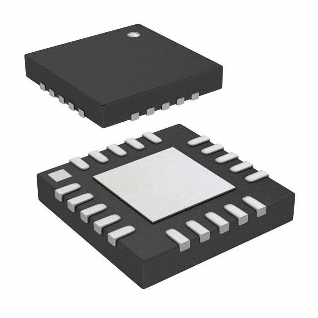
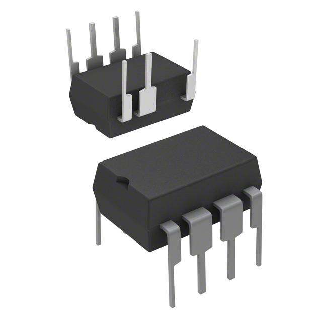
| 描述 | IC DSA 5BIT 50 OHM 20-QFN |
| 产品分类 | |
| 品牌 | Peregrine Semiconductor |
| 数据手册 | |
| 产品图片 |
|
| 产品型号 | 4305-52 |
| rohs | 无铅 / 符合限制有害物质指令(RoHS)规范要求 |
| 产品系列 | UltraCMOS® |
| 其它名称 | 1046-1032-1 |
| 功率(W) | - |
| 容差 | ±0.25dB |
| 封装/外壳 | 20-WFQFN 裸露焊盘 |
| 标准包装 | 1 |
| 衰减值 | 15.5dB |
| 阻抗 | 50 欧姆 |
| 频率范围 | 0 ~ 4GHz |


- 商务部:美国ITC正式对集成电路等产品启动337调查
- 曝三星4nm工艺存在良率问题 高通将骁龙8 Gen1或转产台积电
- 太阳诱电将投资9.5亿元在常州建新厂生产MLCC 预计2023年完工
- 英特尔发布欧洲新工厂建设计划 深化IDM 2.0 战略
- 台积电先进制程称霸业界 有大客户加持明年业绩稳了
- 达到5530亿美元!SIA预计今年全球半导体销售额将创下新高
- 英特尔拟将自动驾驶子公司Mobileye上市 估值或超500亿美元
- 三星加码芯片和SET,合并消费电子和移动部门,撤换高东真等 CEO
- 三星电子宣布重大人事变动 还合并消费电子和移动部门
- 海关总署:前11个月进口集成电路产品价值2.52万亿元 增长14.8%


-50DP-0.5V(81).jpg)
PDF Datasheet 数据手册内容提取
Product Specification PE4305 50 Ω RF Digital Attenuator Product Description 5-bit, 15.5 dB, DC – 4.0 GHz Features The PE4305 is a high linearity, 5-bit RF Digital Step Attenuator (DSA) covering a 15.5 dB attenuation range in 0.5 dB steps, • Attenuation: 0.5 dB steps to 15.5 dB and is pin compatible with the PE430x series. This 50-ohm RF • Flexible parallel andE serial programming DSA provides both parallel (latched or direct mode) and serial interfaces CMOS control interface, operates on a single 3-volt supply and • Latched or direct mode maintains high attenuation accuracy over frequency and • Unique power-up state selection T temperature. It also has a unique control interface that allows • Positive CMOS control logic the user to select an initial attenuation state at power-up. The • High attenuation accuracy and linearity PE4305 exhibits very low insertion loss and low power over temperature and frequency consumption. This functionality is delivered in a 4x4 mm QFN E • Very low power consumpt2ion footprint. • Single-supply operation 1 The PE4305 is manufactured on Peregrine’s UltraCMOS™ • 50 Ω impedance process, a patented variation of silicon-on-insulator (SOI) L • Pin compatible w3ith PE430x series technology on a sapphire substrate, offering the performance • Packaged in a 20 Lead 4x4 mm QFN 4 of GaAs with the economy and integration of conventional CMOS. O E Figure 1. Functional Schematic Diagram Figure 2. Package Type P 4x4 mm 20-Lead QFN Switched Attenuator Array RF Input RF Output S H Parallel Control 5 T ContrBol Logic Interface Serial Control 3 I W Power-Up Control 1 O Table 1. Electrical Specifications @ +25°C, V = 3.0 V E DD Parameter Test Conditions Frequency Minimum Typical Maximum Units C Operation Frequency DC 4000 MHz Insertion Loss2 DC - 2.2 GHz - 1.5 2.25 dB A Any Bit or Bit ±(0.25 + 3% of atten setting) Attenuation Accuracy DC - 2.2 GHz - - dB Combination not to exceed ± 0.4 dB L 1 dB Compression3 1 MHz - 2.2 GHz 30 34 - dBm PTwo-tone inputs Input IP31, 2 1 MHz - 2.2 GHz - 52 - dBm +18 dBm Return Loss DC - 2.2 GHz 15 20 - dB E 50% control to 0.5 dB Switching Speed - - 1 µs of final value R Notes: 1. Device Linearity will begin to degrade below 1Mhz 2. See Max input rating in Table 3 & Figures on Pages 2 to 4 for data across frequency. 3. Note Absolute Maximum in Table 3. Document No. 70-0159-06 │ www.psemi.com ©2003-2008 Peregrine Semiconductor Corp. All rights reserved. Page 1 of 11
PE4305 Product Specification Typical Performance Data @ 25°C, V = 3.0 V DD Figure 3. Insertion Loss Figure 4. Attenuation at Major steps 0 20 E 15.5 dB -1 15 B) d nsertion Loss (dB) --32 alized Attenuation ( 10 8E dB T 2 I insertion loss @ 25 C orm iinnsseerrttiioonn lloossss @@ -8450 C C N 5 4 dB 1 -4 2 dB .5 dB L 1 dB 3 -5 0 4 0 500 1000 1500 2000 2500 3000 3500 4000 0 500 1000 1500 2000 2500 3000 3500 4000 Frequency (MHz) O EFrequency (MHz) P S Figure 5. Input Return Loss at Major Figure 6H. Output Return Loss at Major Attenuation Steps Attenuation Steps T 0 B 0 I W -10 -10 O -20 E -20 B) B) d 8 dB d 1 ( 2 ( S1 C S2 -30 15.5 dB -30 A 15.5 dB -40 -40 L -50 P -50 0 500 1000 1500 2000 2500 3000 3500 4000 0 500 1000 1500 2000 2500 3000 3500 4000 Frequency (MHz) Frequency (MHz) E R ©2003-2008 Peregrine Semiconductor Corp. All rights reserved. Document No. 70-0159-06 │ UltraCMOS™ RFIC Solutions Page 2 of 11
PE4305 Product Specification Typical Performance Data @ 25°C, V = 3.0 V DD Figure 7. Attenuation Error Vs. Frequency Figure 8. Attenuation Error Vs. Attenuation Setting at 10 MHz and 510 MHz 0.6 E 0.2 0.4 0 0.2 T -0.2 B) B) d d Error ( -0.4 15.5 dB Error ( 0 E 10 MHz @ 25 C 2 -0.2 -0.6 510 MHz @ 25 C 10 MHz @ -40 C 1 510 MHz @ -40 C -0.8 -0.4 10 MHz @ 85 C L 3 510 MHz @ 85 C -1 -0.6 4 0 500 1000 1500 2000 2500 3000 3500 4000 0 2 4 6 8 10 12 14 16 Frequency (MHz) O EAttenuation State (dB) P S Figure 9. Attenuation Error Vs. Attenuation Figure 10H. Attenuation Error Vs. Attenuation Setting 1010 MHz and 1210 MHz Setting at 1510 MHz and 2010 MHz T 0.6 B 0.6 I W 0.4 0.4 O 0.2 0.2 E B) B) d d or ( 0 or ( 0 Err C Err -0.2 1010 MHz @ 25 C -0.2 1510 MHz @ 25 C 1010 MHz @ -40 C A 1510 MHz @ -40 C 1010 MHz @ 85 C 1510 MHz @ 85 C 1210 MHZ @ 25 C 2010 MHz @ 25 C -0.4 1210 MHz @ -40 C -0.4 2010 MHz @ -40 C 1210 MHz @ 85 CL 2010 MHz @ 85 C -0.6 P -0.6 0 2 4 6 8 10 12 14 16 0 2 4 6 8 10 12 14 16 Attenuation State (dB) Attenuation State (dB) E Note: Positive Rattenuation error indicates higher attenuation than target value Document No. 70-0159-06 │ www.psemi.com ©2003-2008 Peregrine Semiconductor Corp. All rights reserved. Page 3 of 11
PE4305 Product Specification Typical Performance Data @ 25°C, V = 3.0 V DD Figure 11. Attenuation Error vs. Attenuation Figure 12. 1 dB Compression vs. Frequency Setting at 2010 MHz and 2510 MHz 0.6 40 E 0.4 35 m) 0.2 B T d Error (dB) 0 mpression ( 30 -0.2 22051100 MMHHzz @@ 2255 CC dB Co E 20 dB 2010 MHz @ -40 C 1 0.5 dB 2510 MHz @ -40 C 25 1 1 dB -0.4 2010 MHz @ 85 C 2 dB 2510 MHz @ 85 C L 3 -0.6 20 4 0 2 4 6 8 10 12 14 16 1000 1500 2000 2500 3000 Attenuation State (dB) O EFrequency (MHz) P Figure 13. Input IP3 vs. Frequency S H T 60 B I 55 W 50 O 45 E m) B d 40 P3 ( 0 dB C I 35 0.5 dB 1 dB 2 dB A 30 4 dB 8 dB 15.5 dB 25 L 20 P 500 1000 1500 2000 2500 3000 Frequency (MHz) E Note: Positive Rattenuation error indicates higher attenuation than target value ©2003-2008 Peregrine Semiconductor Corp. All rights reserved. Document No. 70-0159-06 │ UltraCMOS™ RFIC Solutions Page 4 of 11
PE4305 Product Specification Figure 14. Pin Configuration (Top View) Table 3. Absolute Maximum Ratings Symbol Parameter/Conditions Min Max Units 5 D 0. 1 N 2 4 V Power supply voltage -0.3 4.0 V C C G C C DD V + 20 19 18 17 16 VI Voltage on any DC input -0.3 0D.D3 V N/C 1 15 C8 TST Storage temperature range E-65 150 °C RF1 2 20-lead 14 RF2 PIN Input power (50Ω) +30 dBm QFN ESD voltage (Human Body Data 3 4x4 mm 13 P/S VESD Model) 500 V Clock 4 Exposed Solder Pad 12 Vss/GND Exceeding absolute maxTimum ratings may cause per- LE 5 11 GND manent damage. Operation should be restricted to the limits in the Operating Ranges table. Operation be- 6 7 8 9 10 tween operating range maximum and absolute maxi- D C 2 D D mum for extenEded periods may reduce relia2bility. VD N/ UP VD GN P Table 4. Operating Ranges 1 Table 2. Pin Descriptions Parameter Min Typ Max Units Pin No. Pin Name Description L 3 V Power Supply No connect. Can be connected to any DD 2.7 3.0 3.3 V 1 N/C Voltage 4 bias. I Power Supply 2 RF1 RF port (Note 1). DD 100 µA O Current E 3 Data Serial interface data input (Note 4). Digital Input High 0.7xV V DD 4 Clock Serial interface clock input. P Digital Input Low 0.3xV V 5 LE Latch Enable input (Note 2). DD 6 V Power supply pin. Digital Input Leakage 1 µA DD 7 N/C No connect. Can be connSected to any Input PowHer +24 dBm bias. 8 PUP2 Power-up selection bit. Temperature range -40 85 °C T 9 V Power supply pin. DD Exposed Solder Pad Connection 10 GND Ground conBnection. IThe exposed solder pad on the bottom of the package 11 GND Ground connection. W must be grounded for proper device operation. Negative supply voltage or GND 12 V /GND ss connection(Note 3) Electrostatic Discharge (ESD) Precautions 13 P/S OParallel/Serial mode select. When handling this UltraCMOS™ device, observe the same precautions that you would use with other ESD- 14 RF2 RF port (Note 1). E sensitive devices. Although this device contains 15 C8 Attenuation control bit, 8 dB. circuitry to protect it from damage due to ESD, 16 C4 Attenuation control bit, 4C dB. precautions should be taken to avoid exceeding the 17 C2 Attenuation control bit, 2 dB. rate specified in Table 3. 18 GND Ground connection. A 19 C1 Attenuation control bit, 1 dB. Latch-Up Avoidance 20 C0.5 Attenuation control bit, 0.5 dB. Unlike conventional CMOS devices, UltraCMOS™ de- L vices are immune to latch-up. Paddle GND Ground for proper operation Note 1: Both RF ports must be hPeld at 0 VDC or DC blocked with an Switching Frequency external series capacitor. The PE4305 has a maximum 25 kHz switching rate. 2: Latch Enable (LE) hasE an internal 100 kΩ resistor to VDD. Resistor on Pin 3 3: Connect pin 12 to GND to enable internal negative voltage generator. ConnRect pin 12 to VSS (-VDD) to bypass and disable A 10 kΩ resistor on the input to Pin 3 (see Figure 16) internal negative voltage generator. will eliminate package resonance between the RF input 4. Place a 10 kΩ resistor in series, as close to pin as possible to pin and the digital input. Specified attenuation error avoid frequency resonance. See “Resistor on Pin 3” paragraph. versus frequency performance is dependent upon this condition. Document No. 70-0159-06 │ www.psemi.com ©2003-2008 Peregrine Semiconductor Corp. All rights reserved. Page 5 of 11
PE4305 Product Specification Programming Options serially entered into the shift register, a process that is independent of the state of the LE input. Parallel/Serial Selection Either a parallel or serial interface can be used to The LE input controls the latch. When LE is HIGH, control the PE4305. The P/S bit provides this the latch is transparent and the contents of the serial selection, with P/S=LOW selecting the parallel shift register control the attenuator. When LE is interface and P/S=HIGH selecting the serial brought LOW, data in the shift regEister is latched. interface. The shift register should be loaded while LE is held Parallel / Direct Mode Interface LOW to prevent the attenuator value from changing The parallel interface consists of five CMOS- as data is entered. TheT LE input should then be compatible control lines that select the desired toggled HIGH and brought LOW again, latching the attenuation state, as shown in Table 5. new data. The start bit (B5) of the data should always be low to prevent an unknown state in the The parallel interface timing requirements are device. The tEiming for this operation is defined by defined by Figure 18 (Parallel Interface Timing 2 Figure 17 (Serial Interface Timing Diagram) and Diagram), Table 9 (Parallel Interface AC Table 8 (Serial Interface AC Charact1eristics). Characteristics), and switching speed (Table 1). PoLwer-up Control Settings 3 For parallel programming the Latch Enable (LE) The PE4305 always assumes a specifiable should be held LOW while changing attenuation 4 attenuation setting on power-up. This feature exists state control values, then pulse LE HIGH to LOW for both the Serial and Parallel modes of operation, (per Figure 18) to latch new attenuation state into O E and allows a known attenuation state to be device. established before an initial serial or parallel control P word is provided. For direct programming, the Latch Enable (LE) line should be pulled HIGH. Changing attenuation state When the a ttenuator powers up in Serial mode (P/ control values will change device state to nSew H S=1), the five control bits are set to whatever data is attenuation. Direct Mode is ideal for manual control present on the five parallel data inputs (C0.5 to C8). of the device (using hardwire, switches, or jumpers). ThTis allows any one of the 32 attenuation settings to be specified as the power-up state. B I Table 5. Truth Table W When the attenuator powers up in Parallel mode (P/ Attenuation S=0) with LE=0, the control bits are automatically set P/S C8 C4 C2 C1 C0.5 State to one of two possible values. These two values are O 0 0 0 0 0 0 Reference L oss selected by the power-up control bit, PUP2, as 0 0 0 0 0 1 0.5 EdB shown in Table 6 (Power-Up Truth Table, Parallel Mode). 0 0 0 0 1 0 1 dB C 0 0 0 1 0 0 2 dB 0 0 1 0 0 0 4 dB Table 6. Power-Up Truth Table, Parallel A 0 1 0 0 0 0 8 dB Interface Mode 0 1 1 1 1 1 15.5 dB L P/S LE PUP2 Attenuation State Note: Not all 32 possible combinations of C0.5-C8 are shown in table 0 0 0 Reference Loss P 0 0 1 8 dB Serial Interface 0 1 X Defined by C0.5-C8 The PE4305’s seriEal interface is a 6-bit serial-in, parallel-out shift register buffered by a transparent Note: Power up with LE=1 provides normal parallel operation with C0.5-C8, and PUP2 is not active latch. The laRtch is controlled by three CMOS- compatible signals: Data, Clock, and Latch Enable (LE). The Data and Clock inputs allow data to be ©2003-2008 Peregrine Semiconductor Corp. All rights reserved. Document No. 70-0159-06 │ UltraCMOS™ RFIC Solutions Page 6 of 11
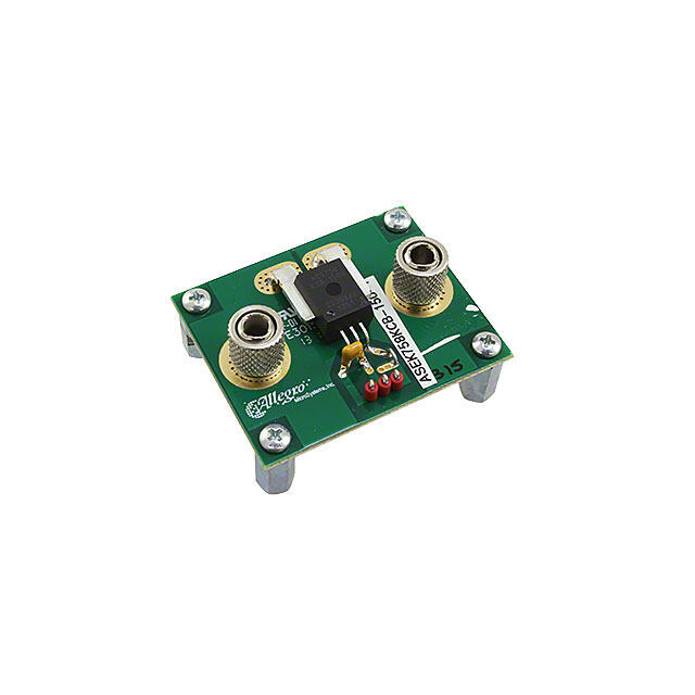
PE4305 Product Specification Evaluation Kit Figure 15. Evaluation Board Layout Peregrine Specification 101/0112 The Digital Attenuator Evaluation Kit board was designed to ease customer evaluation of the PE4305 DSA. J9 is used in conjunction with the supplied DC cable E to supply VDD, GND, and –VDD. If use of the internal negative voltage generator is desired, then connect –VDD (black banana plug) to ground. If an external –VDD is desired, then apply -3V. T J1 should be connected to the LPT1 port of a PC with the supplied control cable. The evaluation software is written to operate the DSA in serial mode, so switch 7 (P/S) on the DIP switch SW1 E 2 should be ON with all other switches off. Using the software, enable or disable each attenuation setting 1 to the desired combined attenuation. The software automatically programs the DSA each time an L 3 attenuation state is enabled or disabled. 4 To evaluate the Power Up options, first disconnect O E the control cable from the evaluation board. The control cable must be removed to prevent the PC port from biasing the control pins. P During power up with P/S=1 high and LE=0 or P/S=0 low and LE=1, the default power-up signal S H attenuation is set to the value present on the five control bits on the five parallel data inputs (C0.5 to FiTgure 16. Evaluation Board Schematic C8). This allows any one of the 32 attenuation Peregrine Specification 102/0144 settings to be specified as the poBwer-up state. I During power up with P/S=0 high and LE=0, the W C0.5 C1 C2 C4 control bits are automatically set to one of two 0 9 8 7 6 possible values presented through the PUP 2 1 1 1 1 interface. These twoO values are selected by the J4 1 N/CC5 C1 GND C2 C4C8 15 C8 J5 power-up control bit, PUP2, as shown in TableE 6. 1 Z=50 Ohm 2 14 Z=50 Ohm 1 RFin U1 RFout Pins 1 and 7 are open and may be connected to any 3 QFN4X4 13 bias. C SMA DATA 10 kohm DATA PS PS SMA 4 12 CLK CLK VNEG D Resistor on Pin 3 A LE 5 LEVDD N/C PUP2 VDD_ GGNDND 11 A 10 kΩ resistor on the input to pin 3 (Figure 16) will 0 6 7 8 9 1 eliminate package resonanceL between the RF input PUP2 pin and the digital input. Specified attenuation error VCC versus frequency performPance is dependent upon this condition. E 100 pF R Note: Resistor on pin 3 is required and should be placed as close to the part as possible to avoid package resonance and meet error specifications over frequency. Document No. 70-0159-06 │ www.psemi.com ©2003-2008 Peregrine Semiconductor Corp. All rights reserved. Page 7 of 11
PE4305 Product Specification Figure 17. Serial Interface Timing Diagram Table 7. 5-Bit Attenuator Serial Programming Register Map LE B5 B4 B3 B2 B1 B0 Clock 0 C8 C4 C2 EC1 C0.5 ↑ ↑ MSB (first in) LSB (last in) Data MSB LSB T tSDSUP tSDHLD tLESUP tLEPW Note: The start bit (B5) must always be low to prevent the attenuator from entering an unknown state. E 2 Figure 18. Parallel Interface Timing Diagram 1 LE L 3 4 O E Parallel Data C8:C0.5 P S H t t LEPW t PDSUP PDHLD T B I Table 8. Serial Interface AC Characteristics Table 9. Parallel Interface AC Characteristics W VDD = 3.0 V, -40° C < TA < 85° C, unless otherwise specified VDD = 3.0 V, -40° C < TA < 85° C, unless otherwise specified Symbol Parameter Min Max Unit Symbol Parameter Min Max Unit O fClk Sfreeqriuael dnacyta ( Nclootcek 1) 10 EMHz tLEPW LE minimum pulse width 10 ns Data set-up time before t 10 ns tClkH Serial clock HIGH time 30 ns PDSUP rising edge of LE C tClkL Serial clock LOW time 30 ns tPDHLD Dfaalltinag h eodldg teim oef LaEft er 10 ns LE set-up time after last tLESUP clock falling edge 1A0 ns t LE minimum pulse width 30 ns LEPW L Serial data set-up time t 10 ns SDSUP before clock rising edge P Serial data hold time t 10 ns SDHLD after clock falling edge E Note: f is verified during the functional pattern test. Serial Clk programming sections of the functional pattern are clocked at 10 MHz to Rverify fclk specification. ©2003-2008 Peregrine Semiconductor Corp. All rights reserved. Document No. 70-0159-06 │ UltraCMOS™ RFIC Solutions Page 8 of 11
PE4305 Product Specification Figure 19. Package Drawing 4.00 INDEX AREA - B - 2.00 E 2.00 X 2.00 0 2.0 T 0 0.25 C 4.0 - A - E 2 0 1 0.8 0.10 C L 3 0.08 C SEATING EXPOSED PAD & PLANE - C - 4 TERMINAL PADS 0.020 0 REF O 0.2 E PP YY 2.00 2.00 T0.50 T0.55 1.00 P 0.435 0.18 35 S 5 6 1H0 1 1 1.00 0.4 0 0 4.0 T 2.0 0.18 B 1 15 I DETAIL A W 20 16 EXPOSED PAD 2 DETAIL A 0.23 0.10 C A B 1 O E 1. Dimension applies to metallized terminal and is measured C between 0.25 and 0.30 from terminal tip. 2. Coplanarity applies to the exposed heat sink slug as well as the terminals. A 3. Dimensions are in millimeters. L P E R Document No. 70-0159-06 │ www.psemi.com ©2003-2008 Peregrine Semiconductor Corp. All rights reserved. Page 9 of 11
PE4305 Product Specification Figure 20. Marking Specifications E 4305 YYWW T ZZZZZ E 2 1 YYWW = Date Code L 3 ZZZZZ = Last five digits of PSC Lot Number 4 O E Figure 21. Tape and Reel Drawing P S H T B I W O E C A Table 10. Ordering Information L Order Code Part Marking Description Package Shipping Method P 4305-00 PE4305-EK PE4305-20MLP 4x4mm-EK Evaluation Kit 1 / Box 4305-51 4305 PE4305G-20MLP 4x4mm-75A Green 20-lead 4x4mm QFN 75 units / Tube E 4305-52 4305 PE4305G-20MLP 4x4mm-3000C Green 20-lead 4x4mm QFN 3000 units / T&R R ©2003-2008 Peregrine Semiconductor Corp. All rights reserved. Document No. 70-0159-06 │ UltraCMOS™ RFIC Solutions Page 10 of 11
PE4305 Product Specification Sales Offices The Americas Peregrine Semiconductor Corporation Peregrine Semiconductor, Asia Pacific (APAC) 9380 Carroll Park Drive Shanghai, 200040, P.R. China San Diego, CA 92121 Tel: +86-21-5836-8276 E Fax: +86-21-5836-7652 Tel: 858-731-9400 Fax: 858-731-9499 Peregrine Semiconductor, Korea #B-2607, Kolon Tripolis, 210 Europe Geumgok-dong, Bundang-gTu, Seongnam-si Gyeonggi-do, 463-943 South Korea Peregrine Semiconductor Europe Tel: +82-31-728-3939 Bâtiment Maine Fax: +82-31-728-3940 13-15 rue des Quatre Vents Peregrine SEemiconductor K.K., Japan 2 F-92380 Garches, France Teikoku Hotel Tower 10B-6 Tel: +33-1-4741-9173 1-1-1 Uchisaiwai-cho, Chiyoda-ku 1 Fax : +33-1-4741-9173 Tokyo 100-0011 Japan Tel: +81-3-3502-5211 L 3 Space and Defense Products Fax: +81-3-3502-5213 4 Americas: Tel: 858-731-9453 O E Europe, Asia Pacific: 180 Rue Jean de Guiramand P 13852 Aix-En-Provence Cedex 3, France Tel: +33-4-4239-3361 Fax: +33-4-4239-7227 S H For a list of representatives in your area, please refer to our Web site at: www.psemi.com T Data Sheet Identification B I W Advance Information The information in this data sheet is believed to be reliable. However, Peregrine assumes no liability for the use of this The product is in a formaOtive or design stage. The data information. Use shall be entirely at the user’s own risk. sheet contains design target specifications for productE development. Specifications and features may change in No patent rights or licenses to any circuits described in this any manner without notice. C data sheet are implied or granted to any third party. Preliminary Specification Peregrine’s products are not designed or intended for use in A The data sheet contains preliminary data. Additional data devices or systems intended for surgical implant, or in other may be added at a later date. Peregrine reserves the right applications intended to support or sustain life, or in any L to change specifications at any time without notice in order application in which the failure of the Peregrine product could to supply the best possible pProduct. create a situation in which personal injury or death might occur. Peregrine assumes no liability for damages, including Product SpecificEation consequential or incidental damages, arising out of the use of its products in such applications. The data sheet contains final data. In the event Peregrine decides to chanRge the specifications, Peregrine will notify The Peregrine name, logo, and UTSi are registered trademarks customers of the intended changes by issuing a DCN and UltraCMOS, HaRP and MultiSwitch are trademarks of (Document Change Notice). Peregrine Semiconductor Corp. Document No. 70-0159-06 │ www.psemi.com ©2003-2008 Peregrine Semiconductor Corp. All rights reserved. Page 11 of 11