ICGOO在线商城 > 射频/IF 和 RFID > RF 评估和开发套件,板 > 4010-KFOBDEV-434
 Datasheet下载
- 型号: 4010-KFOBDEV-434
- 制造商: Silicon Laboratories
- 库位|库存: xxxx|xxxx
- 要求:
| 数量阶梯 | 香港交货 | 国内含税 |
| +xxxx | $xxxx | ¥xxxx |
查看当月历史价格
查看今年历史价格
4010-KFOBDEV-434产品简介:
ICGOO电子元器件商城为您提供4010-KFOBDEV-434由Silicon Laboratories设计生产,在icgoo商城现货销售,并且可以通过原厂、代理商等渠道进行代购。 4010-KFOBDEV-434价格参考。Silicon Laboratories4010-KFOBDEV-434封装/规格:RF 评估和开发套件,板, 。您可以下载4010-KFOBDEV-434参考资料、Datasheet数据手册功能说明书,资料中有4010-KFOBDEV-434 详细功能的应用电路图电压和使用方法及教程。
Silicon Labs 型号为 4010-KFOBDEV-434 的开发套件属于其 RF(射频)评估与开发工具系列,主要面向 434MHz 频段的无线通信应用。该开发套件基于 Silicon Labs 的小无线收发芯片,适用于低功耗、中短距离无线通信场景。

该套件常用于以下应用场景:

1. 遥控器开发:如车库门控制器、遥控开关等,利用其低功耗和高集成度优势,实现稳定可靠的远程控制功能。

2. 家庭自动化系统:包括智能照明、窗帘控制、安防报警等,支持用户构建低成本、低功耗的家庭无线网络。

3. 工业控制与传感器网络:适用于工业环境下的数据采集与控制指令传输,例如温湿度监测、设备状态监控等。

4. 消费类电子产品:如玩具、智能家居配件等,满足对体积小、功耗低、成本可控的产品需求。

5. 无线抄表系统:可用于水表、电表、燃气表等远程数据采集系统中,实现高效的数据传输。

该开发板提供完整的硬件平台和配套软件工具,便于开发者快速评估性能、验证设计,并加速产品开发进程。
| 参数 | 数值 |
| 品牌 | Silicon Labs |
| 产品目录 | 半导体 |
| 描述 | 射频开发工具 Dev Kit with Si4355 Receiver (434MHz) |
| 产品分类 | 工程技术开发工具 |
| 产品手册 | |
| 产品图片 |
|
| rohs | 符合RoHS |
| 产品系列 | 射频/无线开发工具,射频开发工具,Silicon Labs 4010-KFOBDEV-434 |
| 产品型号 | 4010-KFOBDEV-434 |
| 产品 | Development Kits |
| 产品种类 | 射频开发工具 |
| 商标 | Silicon Labs |
| 商标名 | EZRadio |
| 工作电源电压 | 3 V |
| 工具用于评估 | Si4010 |
| 类型 | Key FOB |
| 系列 | 4010-KFOBDEV |
| 频率 | 434 MHz |


- 商务部:美国ITC正式对集成电路等产品启动337调查
- 曝三星4nm工艺存在良率问题 高通将骁龙8 Gen1或转产台积电
- 太阳诱电将投资9.5亿元在常州建新厂生产MLCC 预计2023年完工
- 英特尔发布欧洲新工厂建设计划 深化IDM 2.0 战略
- 台积电先进制程称霸业界 有大客户加持明年业绩稳了
- 达到5530亿美元!SIA预计今年全球半导体销售额将创下新高
- 英特尔拟将自动驾驶子公司Mobileye上市 估值或超500亿美元
- 三星加码芯片和SET,合并消费电子和移动部门,撤换高东真等 CEO
- 三星电子宣布重大人事变动 还合并消费电子和移动部门
- 海关总署:前11个月进口集成电路产品价值2.52万亿元 增长14.8%
PDF Datasheet 数据手册内容提取
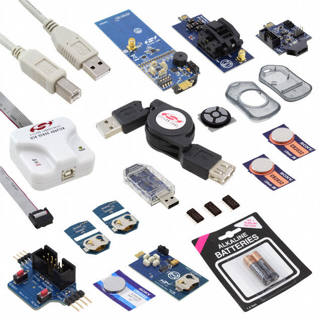
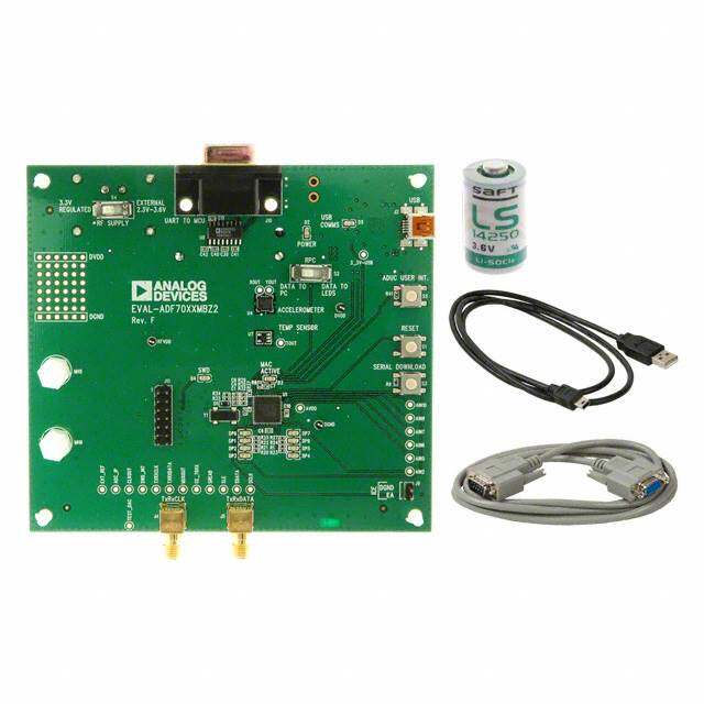
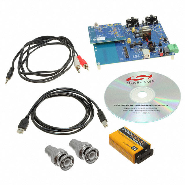
Si4010-DK Si4010 DEVELOPMENT KIT USER’S GUIDE 1. Key Fob Development Platform The Si4010 key fob development platform is a flexible platform for comfortably developing software and testing the whole system using the Silicon Laboratories software development IDE. The platform also allows programming of the NVM on chip. The kit has three versions: one for the 434MHz band (P/N 4010-KFOBDEV-434), one for the 868MHz band (P/N 4010- KFOBDEV-868) and one for the 915MHz band (P/N 4010-KFOBDEV-915). 1.1. Kit Content Table 1. Kit Content Qty Part Number Description 4010-KFOBDEV-434 Si4010 Key Fob Development Kit 434MHz 2 4010-KFOB-434-NF Si4010 key fob demo board 434MHz w/o IC 1 MSC-DKPE1 SOIC/MSOP socketed development board 3 Si4010-C2-GS Si4010-C2-GS transmitter IC, SOIC Package 1 4010-DKPB434-BM Si4010 MSOP key fob development board 434MHz, SMA 1 4355-LED-434-SRX Si4355 RFStick 434MHz receiver board 1 MSC-PLPB_1 Key Fob Plastic Case (translucent grey) 1 MSC-BA5 Programming interface board 1 MSC-BA4 Burning adapter board 1 EC3 USB Debug Adapter 1 Toolstick_BA Toolstick Base Adapter 1 MSC-DKCS5 USB Cable 1 USB extender cable (USBA-USBA) 2 AAA AAA battery 2 CRD2032 CR2032 3V coin battery 4010-KFOBDEV-868 Si4010 Key Fob Development Kit 868MHz 2 4010-KFOB-868-NF Si4010 key fob demo board 868MHz w/o IC 1 MSC-DKPE1 SOIC/MSOP socketed development board 3 Si4010-C2-GS Si4010-C2-GS transmitter IC, SOIC Package 1 4010-DKPB868-BM Si4010 MSOP key fob development board 868 MHz, SMA 1 4355-LED-868-SRX Si4355 RFStick 868MHz receiver board Rev. 0.1 6/12 Copyright © 2012 by Silicon Laboratories Si4010-DK
Si4010-DK Table 1. Kit Content (Continued) 1 MSC-PLPB_1 Key Fob Plastic Case (translucent grey) 1 MSC-BA5 Programming interface board 1 MSC-BA4 Burning adapter board 1 EC3 USB Debug Adapter 1 Toolstick_BA Toolstick Base Adapter 1 MSC-DKCS5 USB Cable 1 USB extender cable (USBA-USBA) 2 AAA AAA battery 2 CRD2032 CR2032 3V coin battery 4010-KFOBDEV-915 Si4010 Key Fob Development Kit 915MHz 2 4010-KFOB-915-NF Si4010 key fob demo board 915MHz w/o IC 1 MSC-DKPE1 SOIC/MSOP socketed development board 3 Si4010-C2-GS Si4010-C2-GS transmitter IC, SOIC Package 1 4010-DKPB915-BM Si4010 MSOP key fob development board 915 MHz, SMA 1 4355-LED-915-SRX Si4355 RFStick 915MHz receiver board 1 MSC-PLPB_1 Key Fob Plastic Case (translucent grey) 1 MSC-BA5 Programming interface board 1 MSC-BA4 Burning adapter board 1 EC3 USB Debug Adapter 1 Toolstick_BA Toolstick Base Adapter 1 MSC-DKCS5 USB Cable 1 USB extender cable (USBA-USBA) 2 AAA AAA battery 2 CRD2032 CR2032 3V coin battery 2 Rev. 0.1
Si4010-DK 1.1.1. Burning Adapter (P/N MSC-BA4) The programming interface board serves as an interface in between the debug adapter and the Socketed Key Fob Development Board or the Development Key Fob. It provides 6.5V for NVM programming. The power source is activated by a sliding switch on the board. It is required when the user wants to program the internal NVM memory on the chip. The programming interface board contains an 8-pin header, to which GPIO0 to GPIO5, along with power and ground, are connected from the development boards. Therefore, the user can tap to that header to control or monitor the chip pins. 1.1.2. Si4010 Socketed Key Fob Development Board (P/N MSC-DKPE1) Socketed (both SOIC and MSOP) key fob board with SMA connector. Rev. 0.1 3
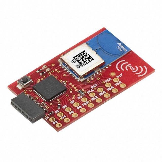
Si4010-DK 1.1.3. Si4010 MSOP Key Fob Development Board 434MHz, SMA (P/N 4010-DKPB434-BM) This development board has an unburned soldered Si4010, five push buttons, matched 50 SMA RF output, battery clip, and battery switch. This board allows running user application from RAM during program development even while board is disconnected and powered by the battery. The SMA output connector allows wired measurements of the RF output signal. Note: Instead of this board, some 434MHz development kits may contain the pcb antenna version of this board, described in "1.2.2. Si4010 Key Fob Development Board 434MHz" on page 7. 1.1.4. Si4355 RFStick 434MHz receiver board (P/N 4355-LED-434-SRX) Receiver board factory programmed with the simple receiver program srx_demo. Can be used for link testing with Si4010 programmed with the rke_demo. 1.1.5. Programming Interface Board (P/N MSC-BA5) Adapter board for interfacing customer PCB to the debug adapter. 4 Rev. 0.1
Si4010-DK 1.1.6. 4010 Key Fob Demo Board 434MHz without IC (P/N 4010-KFOB-434-NF) 1.1.7. Key Fob Plastic Case (translucent grey) (P/N MSC-PLPB_1) 1.1.8. Toolstick Base Adapter (P/N Toolstick_BA) Debugging adapter compatible with Si4355 RFstick receiver board and the Si4010 development boards. 1.1.9. Si4010 sample, SOIC package (P/N Si4010-C2-GS) 1.1.10. USB Cable (P/N MSC-DKCS5) Cable to connect EC3 Debug Adapter to PC. Rev. 0.1 5
Si4010-DK 1.1.11. EC3 Debug Adapter (P/N EC3) Silicon Labs debugging adapter, used by other Silicon Labs’ MCU products as well, compatible with the development platform. 6 Rev. 0.1
Si4010-DK 1.2. Other Boards The following boards are not part of the development kit but can be ordered separately from Silicon Labs. Part Number Description 4010-DKPB434-BS Si4010 SOIC key fob development board 434MHz, SMA 4010-DKPB_434 Si4010 key fob development board 434MHz 4010-DKMX_434 Si4010 matrix keyboard development board 434MHz 4010-KFOB-315-NF Si4010 key fob demo board 315MHz w/o IC 1.2.1. Si4010 SOIC Key Fob Development Board 434MHz, SMA This board is similar to the board described in “1.1.3. Si4010 MSOP Key Fob Development Board 434MHz, SMA (P/N 4010-DKPB434-BM)” but contains the SOIC package version of the Si4010. 1.2.2. Si4010 Key Fob Development Board 434MHz This is also a key fob development board, but with a pcb antenna instead of the SMA connector. Rev. 0.1 7
Si4010-DK 1.3. Usage of the Key Fob Development Platform The Silicon Labs IDE communicates with the USB Debug Adapter through the USB bus. The following debugging scenarios are possible: 1. EC3 debug adapter Burning adapterSi4010 socketed key fob development board This setup is suitable for downloading, running, and debugging the program in RAM or burning the program in the NVM and running it. The antenna or measuring instrument can be connected through an SMA connector. Since sockets on board allow use of unsoldered ICs, this is the ideal scenario for burning the NVM memory of Si4010. 2. EC3 debug adapter Burning adapter Si4010 MSOP key fob development board This setup is suitable for downloading, running, and debugging the program in RAM. This board has a PCB antenna and battery, so after downloading the program and starting the execution by disconnecting in the IDE, the board can be physically disconnected from the programming interface and tested in mobile form. A switch is provided on the board to connect/disconnect the battery. The Toolstick Base Adapter can be also used in the two above scenarios as a debug adapter. It can be connected to the pcb edge connector of the burning adapter. Note: Although burning is also possible with this setup, it is not practical since Si4010 is soldered on the key fob development board. 8 Rev. 0.1
Si4010-DK 3. EC3 debug adapter Programming adapter User’s own application In this setup, the user can incorporate the debugging capabilities into the final application using a cheap 4-pin header connection. 2. Debugging an Application To debug an application the user is provided with the Silicon Laboratories IDE (Integrated Development Environment). The IDE has an integral help. This section is not a user manual for the IDE, but highlights the items which are important when working with the IDE. 2.1. Installing the IDE and USB Debug Adapters Download the Silicon Labs IDE (Integrated Dvelopment Environment) from the following URL: http://www.silabs.com/products/mcu/Pages/SiliconLaboratoriesIDE.aspx and install it on your computer. The IDE gets installed into its own directory. The main executable file is IDE.exe. The IDE works with the USB Debug Adapter or the Toolstick Base Adapter, shown in the section above. When the IDE recognizes the Silicon Labs USB debug adapters, it queries whether its internal firmware is compatible with the Si4010. If not, then it notifies the user and requests permission to update the adapter's firmware. Silicon Labs also provides a program, usb_debug_adapter_firmware_reset.exe, to clear the adapter's firmware manually before connection to the IDE. The program resides in the same directory as the IDE main executable. With the Si4010 debugging chain it is required that the manual adapter firmware clearing is done for each USB adapter before using the key fob debugging chain. That operation needs to be done only once per USB Debug Adapter. The IDE will then program the correct firmware into the adapter. The reset firmware executable will scan USB ports and give the user a list of connected Silicon Labs USB adapters. The USB Debug Adapter name starts with EC. Users can have more than one USB adapter connected to the computer. 2.2. Keil toolchain integration The project files in examples assume that the Keil toolchain is installed into: C:\Keil directory. The location of the Keil toolchain can be easily changed in the Silabs IDE in the Project—Tool Chain Integration menu. An evaluation version of the Keil toolchain can be downloaded from the Keil website at http://www.keil.com/. This free version has a 2kB code limitation and starts the code at the 0x0800 address. The Keil free evaluation version can be unlocked to become a 4kB version with no code placement limitation by following the directions given in application note AN104 about Keil toolchain integration and license management. Unlock code can be found on the WDS CDROM in the root folder in the Keil_license_number.txt file. Contact your Silicon Laboratories sales representative or distributor for application assistance. Rev. 0.1 9
Si4010-DK 2.3. IDE Features The IDE allows the following: 1. Download the OMF-51 linker output format (Keil BL51 linker output, for example) and match the source code lines with the compiled file. This allows source code debugging, including variable value viewing, set- ting breakpoints, single-stepping, etc. Note that the output of the Keil LX51 linker is not understood by the IDE. 2. Download the IntelHEX file for the application. When using the IntelHEX file the source code debugging is not available. The user can set a breakpoint for a specific code address by going through the Debug Breakpoints (Alt+B) menu item. The user can also single-step through the disassembly of the loaded code. 3. Setting at least 4 breakpoints with a possible maximum of 8. The actual number of breakpoints available is determined by the IDE from the factory setting of the chip. 4. Single-stepping through the disassembly of the code. If the OMF file is loaded, the single-stepping is matched with the source code. 5. Viewing and changing variables, SFR registers, XREG registers, and the contents of both DATA/IDATA RAM and CODE/XDATA RAM on the fly during debugging. When the changes are made by the user in the corresponding windows, the user must press the Refresh Values (Alt+R) button on the toolbar to update the values in the device. Just changing values in the IDE will not automatically update them in the device. 2.4. IDE Debugging Session The typical IDE debugging session consists of the following sequence: 1. Connect the IDE to the chip by hitting the Connect or invoking menu Debug Connect menu item. 2. Download the OMF file either by hitting the Download code (Alt+D) toolbar button or from the Debug Download object code menu item. The latter also allows IntelHEX download, but without the source code debugging capability. 3. After the code download, the device is automatically halted at address 0x0000 in CODE/XDATA RAM. Then the user can set breakpoints, single-step, animate, etc. 4. The user can hit the Reset (Ctrl+R) toolbar button any time the device is halted (not running). The internal digital system level reset is invoked and the device goes through the boot sequence. The previously loaded code by the user into the CODE/XDATA RAM is preserved and the device is halted at the address 0x0000 of CODE/XDATA RAM. 5. When a bug is found, the user can download a new OMF file whenever the device is halted. There is no need to disconnect the device from the debug chain or to hit reset. The download, item 2 above, will auto- matically reset the device after the OMF/IntelHEX new code download is finished. It is very important to note that whenever the Disconnect toolbar button is hit or the Debug Disconnect menu item is invoked, the debugging chain does the following: • Enables the LED driver. During the debugging sessions the LED current driver is forcibly disabled. • Clears all the breakpoints. • Releases the device from halt and lets it run from the point when it was halted. 2.5. Important Note about Single-Stepping Over ROM Code Single-stepping through the ROM code is disabled. Whenever the user encounters the call to the ROM API functions he or she should use the Step Over (F10) toolbar button rather than the Step (F11) or Multiple Step button. Even though single-stepping through the ROM API function using the Step (F11) button works from the user’s point of view, the CPU timing is modified and real-time performance is not guaranteed when using the Step (F11) or Multiple Step buttons over the ROM API functions. Therefore, it is highly recommended to use the Step Over (F10) toolbar button when stepping over the ROM API functions in IDE. Single-stepping over the bMtp_Write() function using Step (F11) or Multiple Step buttons may yield unpredictable results in the MTP (EEPROM) and is highly discouraged. One should use the Step Over (F10) tool, run to cursor, or setting a breakpoint when debugging around the MTP write function. 10 Rev. 0.1
Si4010-DK 2.6. Device Version 1. The device ID information can be read through the IDE through Views Debug Windows Si4010 XREG Regs. The last item bREV_ID is the device revision. The user can also call the API function bSys- _GetRevId(). 2. The trim version can be read by the Silicon Labs IDE as External Memory through Views Debug Win- dows -> External Memory at location 0x11D6. There is a macro bSys_TrimId_c defined in the headers for use in customer code as well. The user needs to know the TrimId before writing any code, so the man- ual access to it is adequate. The trim version will rarely change and customers will be notified about the change.The provided NVM burner program reads both the bREV_ID device revision and the trim version bSys_TrimId in the [Device] tab after the burner is connected to the device. 2.7. Debugging Application which Drives LED To maximize utilization of the package pins, the LED current driver output is shared with the debug chain clock signal C2CLK. To share the functionality and be able to use the IDE for debugging there are some limitations to note and rules to follow. The following figure shows the recommended connection of the USB 10-pin debug header to the device in the user application. Note: The LED must be isolated by the 470 resistor for the debug chain to work. Rev. 0.1 11
Si4010-DK Facts about using the LED with IDE chain: 1. The IDE chain can connect to the device only if the LED current driver is off and the LED is not lit. 2. Once the IDE chain is connected to the device it blocks the device LED driver. Therefore, the application can be written in a normal fashion using LED as desired in the final application without worry of being dis- connected from the debug chain. The only limitation is that the LED will not be lit from the application during the IDE debug session. The user will still observe LED activity, but that activity is related to the debug chain communicating with the device, not the user application driving the LED. 3. Once the IDE chain is disconnected from the device (for example, by pressing the Disconnect button in the IDE), the device is released from halt and at the same time the blocking of the LED driver is removed. From that point on, the application behaves and runs as a regular application and the LED activity reflects what the application desires to do with the LED. 4. If the user wants to reconnect the IDE to the device the only requirement is that the LED must not be lit by the application and the C2 debug interface must be active, not being actively turned off by the application. Therefore, if the device user software is stuck in an infinite loop and driving the LED constantly or the C2 interface was turned off by the application, the IDE chain will not be able to connect to the device. In such a situation, the device power has to be cycled to invoke internal power on reset. (See item 1 above.) Cycling the power to the part in this context means either physical removal of the power to the device or calling the vSys_Shutdown() function from within the application, which achieves the same result. 2.8. Hardware Issue with Debugging LED Application There is an issue with the LED turning on and off and the functionality of the GPI04. There is no issue when the part is programmed as the Run part and runs the final application code. Therefore, the issue affects only the application development. There are several possible software workarounds, depending on the approach the user wants to take. 2.8.1. Application LED Control The user can control the LED intensity and whether the LED is on or off. The LED intensity has 4 values, 0 to 3: Off, 0.3mA, 0.6mA, and 1mA current. The user can set the intensity any time, but the LED is not going to be turned on until the GPIO_LED is set to 1. The GPIO_LED is an alias for the P0.5 bit. After the reset the P0.5 bit is set to 1, so it is recommended that the user use GPIO_LED = 0 at the beginning of the user application. To turn the LED off at the very beginning of the user application: /* Clear the GPIO_LED.. reset will set this bit! */ GPIO_LED = 0; To turn the LED on and off inside the user application: /* Set LED intensity .. acceptable values are 0 (off) or 1, 2, and 3 */ vSys_LedIntensity( 3 ); … /* To turn the LED on at currently set intensity */ GPIO_LED = 1; … /* To turn the LED off, keep the intensity setting */ GPIO_LED = 0; 12 Rev. 0.1
Si4010-DK The intensity setting can be changed any time, even when the GPIO_LED = 1. This is basically how the LED control operates. This approach will work when the part status is finalized as the Run device, since for that program level the C2 interface is turned off after the boot-by-boot routine. However, when the code above is used for a device in the Factory or User programming state, then the GPIO4 will stop working after the first LED blink. The LED must be seen to be turned on and off by the application (to blink) to experience this problem. 2.8.2. Solution 1: Living with the Limitation The simplest solution is to know about the issue and decide to live with it. After the first LED blink, the GPI04 will not work. In this scenario, the user may decide to test the GPI04 only when the part is fully programmed as the Run part. 2.8.3. Solution 2: Controlled Compilation The user may use a #define C statement to define a LED "on" value. For button press debugging purposes when the LED can be off the code is compiled with value set as 0, so the LED will never light up and the GPIO4 will always function. For debugging the LED, and for final application compilation for the Run state of the device, the user will compile the application with the LED "on" value set to 1. For example: #ifdef DEBUG #define gLedOnValue_c 0 #else #define gLedOnValue_c 1 #endif /* Clear the GPIO_LED off after reset .. reset will set this bit! */ GPIO_LED = 0; /* Set LED intensity .. acceptable values are 0 (off) or 1, 2, and 3 */ vSys_LedIntensity( 3 ); … /* Turn the LED on at currently set intensity */ GPIO_LED = gLedOnValue_c; … /* Turn the LED off, keep the intensity setting */ GPIO_LED = 0; One advantage of this solution is that the code size is identical in both cases, Debug or Run. Cycling the power to the part in this context means either physical removal of the power to the device or calling the vSys_Shutdown() function from within the application, which achieves the same result. 2.8.4. Solution 3: Dynamic C2 Disable (Recommended) The GPI04 issue manifests itself when the LED is actually being turned on and off from the application. The LED physically blinks and is not blocked from being lit up by an application being connected to the IDE debug chain, and the C2 interface is active and enabled. Rev. 0.1 13
Si4010-DK If we disable the C2 interface when the device is not connected to the IDE chain, and before the LED is turned off when lit, then there will not be the GPIO4 problem. To do that the user must add the following function to the user application to turn the LED on. C function to turn the LED on: /* *------------------------------------------------------------------------------ * * INCLUDES: */ #include "si4010.h" /* *============================================================================== * * VISIBLE FUNCTIONS: */ void vLedOn ( void ) /*------------------------------------------------------------- * * FUNCTION DESCRIPTION: * Turn LED on with disabling of the C2. * The C2 is disabled only if the part is not connected * to the IDE debugging chain. * *------------------------------------------------------------- */ { /* *------------------------------------------------------------- * VARIABLES: *------------------------------------------------------------- */ GPIO_LED = 1; if ( 0 != (RBIT_DATA & M_GPIO_LED_DRIVE) ) { PROT0_CTRL |= M_C2_OFF; } } 14 Rev. 0.1
Si4010-DK /* *------------------------------------------------------------------------------ */ Assembly version of the same function, assuming that the file name is ledon.a51 for Keil toolchain. ;------------------------------------------------------------------------------ ; ; INCLUDES: ; $NOLIST $INCLUDE (si4010.inc) $LIST ;--------------------------------------------------------------------------- ; ; SEGMENTS: ; ; Assumes file name to be ledon.a51 .. capitalized LEDON is the file name NAME LEDON ?PR?vLedOn?LEDON SEGMENT CODE ;--------------------------------------------------------------------------- ; ; EXTERNALS AND PUBLIC: ; PUBLIC vLedOn ;--------------------------------------------------------------------------- ; ; CODE: ; RSEG ?PR?vLedOn?LEDON vLedOn: setb GPIO_LED mov A, RBIT_DATA jnb ACC.B_GPIO_LED_DRIVE, NoC2Disable orl PROT0_CTRL, #M_C2_OFF NoC2Disable: Rev. 0.1 15
Si4010-DK ret ; -- End of assembly END ; ;--------------------------------------------------------------------------- ; The function is able to determine whether the device is connected to the IDE chain. If it is not connected, then the function turns the C2 interface off. Once that is done it is not possible to turn the C2 interface back on unless the power to the device, or at least to the digital portion of the device, is cycled. See the discussion below about advantages and disadvantages. The following is an example of how to use the vLedOn() function: /* Clear the GPIO_LED off after reset .. reset will set this bit! */ GPIO_LED = 0; /* Set LED intensity .. acceptable values are 0 (off) or 1, 2, and 3 */ vSys_LedIntensity( 3 ); … /* Turn the LED on at currently set intensity */ vLedOn(); … /* Turn the LED off, keep the intensity setting */ GPIO_LED = 0; Following are the advantages and disadvantages of this solution: Advantages: 1. Uniform code, no need for conditional compilation, the GPIO4 and LED will function as expected under all scenarios. 2. The user can use the GPIO_LED=1 in the code, which will block the GPIO4. But subsequent call to vLedOn() will clear the blocking of the GPIO4 and it will start functioning normally again. Disadvantages: 1. Once the LED is physically blinked then it is not possible for the IDE to connect to the part until the power is cycled or the vSys_Shutdown() is called from within the application. It is up to the user to make sure that the power is cycled. 2. If the part is programmed as the User part with the option to execute the user code after the boot automatically without stopping, then the user application must not use the vLedOn() function just to blink LED without a user input. If the application blinks the LED on its own, then the IDE will not be able to connect to the part, since the C2 interface is disabled at the time when the LED is turned on. If the user does not use the option to execute user code without stopping after the boot, there is not a problem since the device will load User code after the reset and wait for further instructions, essentially waiting for the IDE to connect to it without executing the User code. 16 Rev. 0.1
Si4010-DK 3. The vLedOn() function code is bigger than simple GPIO_LED=1 and is not necessary for the Run part, so conditional compilation for LED bug may still be an option. One recommendation for using the vLedOn() function is that the user application would include monitoring of several buttons pressed simultaneously. If that combination happens, then the vSys_Shutdown() is invoked and the IDE chain would be able to connect to the part again. That would satisfy the power cycling requirement without actually cycling the physical power to the device. 2.9. Notes about USB Adapter Use The following facts are worth noting when using the IDE debug chain: 1. Whenever the Reset button is pressed on the IDE, the system reset is invoked and the part goes through a boot sequence. 2. Every time the new code, in OMF or HEX format, is downloaded to the part through the IDE, the IDE issues a system reset and the device reboots. The content of the RAM memories is not touched by the boot, with the exception of the API reserved regions in CODE/XDATA and DATA/IDATA memories. The register banks RB0, RB1, and RB3 are cleared by the boot routine. 3. Whenever the ToolStick adapter is directly connected to the key fob design platform and the IDE is con- necting to the part, the GPIO0 will be forcibly driven to 1 for about 260ms around the beginning of the con- nection sequence. In the Silicon Labs-provided key fob platform, the GPIO0 isolated by a resistor, then if the user is pressing a GPIO0 button during the connection sequence, the GPIO0 value will be viewed as 1 by the internal CPU during the IDE connection to the device. 4. It is recommended that the user uses the Burning adapter board along with the USB Debug Adapter. Rev. 0.1 17
Si4010-DK 3. Examples provided There are 5 demonstration examples provided with the development kit documentation pack: 1. aes_demo 2. fcast_demo 3. fstep_demo 4. tone_demo 5. keyfob_demo 6. rke_demo All are precompiled and ready to be used without compilation for convenience. The user just needs to go to the <name>_demo/bin directory and open the Silicon Labs IDE *.wsp project file by the Silicon Labs IDE. Each demo can be built and debugged from within the Silicon Labs IDE. 3.1. AES demo-aes_demo AES example with timer usage example. The timer counts the number of system clock cycles needed to run encryption, decryption key preparation, and decryption. 3.2. Frequency casting demo-fcast_demo This example shows the main flow when using the main vFCast_Tune tuning function. It also shows how to transmit a predefined data packet when a button is pressed. The buttons are not debounced in this simple example. 3.3. Frequency casting two step demo-fstep_demo This example shows the main flow when the user wants to switch in between several frequencies fast. It is possible to call vFCast_Tune()for several frequencies in advance, collect the information calculated, and then just quickly apply it during transmission. This is for the cases when the 5-6ms time spent in vFCast_Tune() is prohibitive for switching in between frequencies. 3.4. Tone (CW) generation demo-tone_demo This example shows the steps to generate continuous wave (tone) at a desired frequency. There are two main files compiled to two separate example applications: tone_demo Run main tune vFCast_Tune once, then use only fine tuning to track the temperature changes. tone_demo_ptune Periodic tuning, run main tune vFCast_Tune every minute and use the fine tuning only in between the main tuning events. However, there will be about 6ms interruption of the output during the main tuning, once per minute. The Keil µVision project tone_demo.Uv2 covers both targets: tone_demo tone_demo_ptune For the Silicon Labs IDE there is only one target per *.wsp file, so there are two project files: tone_demo.wsp tone_demo_ptune.wsp 18 Rev. 0.1
Si4010-DK 3.5. Simple key fob demo-keyfob_demo This example demonstrates a basic key fob application transmitting a packet for every button push. Packets can be received by an 4355-LED-XXX-SRX board. Buttons are debounced using the Button Service API functions. 3.6. RKE key fob demo-rke_demo An advanced key fob demo using AES encryption, rolling counter in MTP memory, battery voltage measurement, and production ID of chip as node address. This is the firmware used in the Si4010 Demo Key Fobs, available in Silicon Labs key fob demo kits. Rev. 0.1 19
Simplicity Studio One-click access to MCU tools, documentation, software, source code libraries & more. Available for Windows, Mac and Linux! www.silabs.com/simplicity MCU Portfolio SW/HW Quality Support and Community www.silabs.com/mcu www.silabs.com/simplicity www.silabs.com/quality community.silabs.com Disclaimer Silicon Laboratories intends to provide customers with the latest, accurate, and in-depth documentation of all peripherals and modules available for system and software implementers using or intending to use the Silicon Laboratories products. Characterization data, available modules and peripherals, memory sizes and memory addresses refer to each specific device, and "Typical" parameters provided can and do vary in different applications. Application examples described herein are for illustrative purposes only. Silicon Laboratories reserves the right to make changes without further notice and limitation to product information, specifications, and descriptions herein, and does not give warranties as to the accuracy or completeness of the included information. Silicon Laboratories shall have no liability for the consequences of use of the information supplied herein. This document does not imply or express copyright licenses granted hereunder to design or fabricate any integrated circuits. The products must not be used within any Life Support System without the specific written consent of Silicon Laboratories. A "Life Support System" is any product or system intended to support or sustain life and/or health, which, if it fails, can be reasonably expected to result in significant personal injury or death. Silicon Laboratories products are generally not intended for military applications. Silicon Laboratories products shall under no circumstances be used in weapons of mass destruction including (but not limited to) nuclear, biological or chemical weapons, or missiles capable of delivering such weapons. Trademark Information Silicon Laboratories Inc., Silicon Laboratories, Silicon Labs, SiLabs and the Silicon Labs logo, CMEMS®, EFM, EFM32, EFR, Energy Micro, Energy Micro logo and combinations thereof, "the world’s most energy friendly microcontrollers", Ember®, EZLink®, EZMac®, EZRadio®, EZRadioPRO®, DSPLL®, ISOmodem ®, Precision32®, ProSLIC®, SiPHY®, USBXpress® and others are trademarks or registered trademarks of Silicon Laboratories Inc. ARM, CORTEX, Cortex-M3 and THUMB are trademarks or registered trademarks of ARM Holdings. Keil is a registered trademark of ARM Limited. All other products or brand names mentioned herein are trademarks of their respective holders. Silicon Laboratories Inc. 400 West Cesar Chavez Austin, TX 78701 USA http://www.silabs.com
Mouser Electronics Authorized Distributor Click to View Pricing, Inventory, Delivery & Lifecycle Information: S ilicon Laboratories: 4010-KFOBDEV-434 4010-KFOBDEV-868 4010-KFOBDEV-915