
 Datasheet下载
- 型号: 25LC080A-E/SN
- 制造商: Microchip
- 库位|库存: xxxx|xxxx
- 要求:
| 数量阶梯 | 香港交货 | 国内含税 |
| +xxxx | $xxxx | ¥xxxx |
查看当月历史价格
查看今年历史价格
25LC080A-E/SN产品简介:
ICGOO电子元器件商城为您提供25LC080A-E/SN由Microchip设计生产,在icgoo商城现货销售,并且可以通过原厂、代理商等渠道进行代购。 25LC080A-E/SN价格参考。Microchip25LC080A-E/SN封装/规格:存储器, EEPROM 存储器 IC 8Kb (1K x 8) SPI 10MHz 8-SOIC。您可以下载25LC080A-E/SN参考资料、Datasheet数据手册功能说明书,资料中有25LC080A-E/SN 详细功能的应用电路图电压和使用方法及教程。
Microchip Technology的25LC080A-E/SN是一款8K位(1K x 8)串行EEPROM存储器,广泛应用于各种需要非易失性数据存储的场景。以下是其主要应用场景:

 1. 消费电子
   - 家电设备:如微波炉、洗衣机、空调等,用于存储用户设置、工作模式、故障记录等信息。即使断电,这些数据也能保存在EEPROM中,确保设备重启后仍能恢复到之前的设置。
   - 智能家居设备:例如智能音箱、智能灯泡等,用于存储配置参数、网络设置、用户偏好等信息。

 2. 工业控制
   - 自动化系统:在PLC(可编程逻辑控制器)、SCADA系统中,用于存储程序代码、配置参数、校准数据等。由于EEPROM具有良好的耐久性和可靠性,适合在工业环境中长期使用。
   - 传感器模块:用于存储传感器的校准系数、测量数据等,确保传感器在不同环境下能够准确工作。

 3. 通信设备
   - 网络设备:如路由器、交换机等,用于存储MAC地址、IP地址、配置文件等关键信息,确保设备在网络中的唯一性和稳定性。
   - 无线模块:如蓝牙、Wi-Fi模块,用于存储固件版本、连接参数、安全密钥等,确保设备能够稳定连接和通信。

 4. 医疗设备
   - 便携式医疗设备:如血糖仪、血压计等,用于存储用户的健康数据、校准信息等,方便用户或医生随时查看历史记录。
   - 诊断仪器:如心电图机、超声波设备等,用于存储设备的工作参数、患者信息等,确保设备能够在不同使用场景下保持一致的性能。

 5. 汽车电子
   - 车载信息系统:如导航系统、娱乐系统等,用于存储地图数据、用户偏好、车辆设置等信息,确保用户在每次启动车辆时都能获得个性化的体验。
   - 发动机控制系统:用于存储发动机的工作参数、故障代码等,帮助技术人员快速诊断问题并进行维修。

 6. 物联网(IoT)
   - 传感器节点:用于存储传感器采集的数据、节点ID、通信协议等信息,确保节点能够在复杂的网络环境中正常工作。
   - 边缘计算设备:用于存储中间计算结果、设备状态等信息,减少与云端的交互频率,提升系统的响应速度。

总之,25LC080A-E/SN凭借其低功耗、高可靠性和易于集成的特点,适用于多种需要非易失性数据存储的应用场景,特别是在对数据保存有较高要求的领域中表现出色。
| 参数 | 数值 |
| 产品目录 | 集成电路 (IC)半导体 |
| 描述 | IC EEPROM 8KBIT 10MHZ 8SOIC电可擦除可编程只读存储器 8k 1kx8 16B Pg -2.5V |
| 产品分类 | |
| 品牌 | Microchip Technology |
| 产品手册 | |
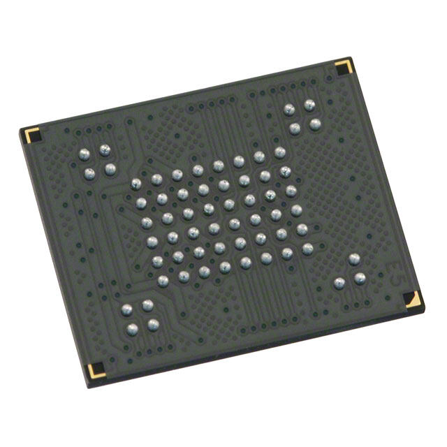
| 产品图片 |
|
| rohs | 符合RoHS无铅 / 符合限制有害物质指令(RoHS)规范要求 |
| 产品系列 | 内存,电可擦除可编程只读存储器,Microchip Technology 25LC080A-E/SN- |
| 数据手册 | http://www.microchip.com/mymicrochip/filehandler.aspx?ddocname=en011767 |
| 产品型号 | 25LC080A-E/SN |
| 产品种类 | 电可擦除可编程只读存储器 |
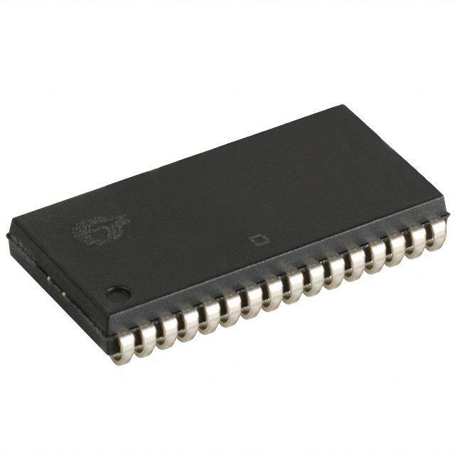
| 供应商器件封装 | 8-SOIC N |
| 包装 | 管件 |
| 商标 | Microchip Technology |
| 存储器类型 | EEPROM |
| 存储容量 | 8 kbit |
| 安装风格 | SMD/SMT |
| 封装 | Tube |
| 封装/外壳 | 8-SOIC(0.154",3.90mm 宽) |
| 封装/箱体 | SOIC-8 |
| 工作温度 | -40°C ~ 125°C |
| 工作电流 | 6 mA |
| 工作电源电压 | 2.5 V, 5.5 V |
| 工厂包装数量 | 100 |
| 接口 | SPI 串行 |
| 接口类型 | SPI |
| 数据保留 | 200 yr |
| 最大工作温度 | + 125 C |
| 最大工作电流 | 6 mA |
| 最大时钟频率 | 10 MHz |
| 最小工作温度 | - 40 C |
| 标准包装 | 100 |
| 格式-存储器 | EEPROMs - 串行 |
| 电压-电源 | 2.5 V ~ 5.5 V |
| 电源电压-最大 | 5.5 V |
| 电源电压-最小 | 2.5 V |
| 组织 | 1 k x 8 |
| 访问时间 | 50 ns |
| 速度 | 10MHz |


- 商务部:美国ITC正式对集成电路等产品启动337调查
- 曝三星4nm工艺存在良率问题 高通将骁龙8 Gen1或转产台积电
- 太阳诱电将投资9.5亿元在常州建新厂生产MLCC 预计2023年完工
- 英特尔发布欧洲新工厂建设计划 深化IDM 2.0 战略
- 台积电先进制程称霸业界 有大客户加持明年业绩稳了
- 达到5530亿美元!SIA预计今年全球半导体销售额将创下新高
- 英特尔拟将自动驾驶子公司Mobileye上市 估值或超500亿美元
- 三星加码芯片和SET,合并消费电子和移动部门,撤换高东真等 CEO
- 三星电子宣布重大人事变动 还合并消费电子和移动部门
- 海关总署:前11个月进口集成电路产品价值2.52万亿元 增长14.8%


PDF Datasheet 数据手册内容提取
25AA080A/B, 25LC080A/B 8K SPI™ Bus Serial EEPROM Device Selection Table Part Number VCC Range Page Size Temp. Ranges Packages 25LC080A 2.5-5.5V 16 Byte I, E P, SN, ST, MS 25AA080A 1.8-5.5V 16 Byte I P, SN, ST, MS 25LC080B 2.5-5.5V 32 Byte I, E P, SN, ST, MS 25AA080B 1.8-5.5V 32 Byte I P, SN, ST, MS Features Description (cid:127) Max. clock 10 MHz The Microchip Technology Inc. 25AA080A/B, * (cid:127) Low-power CMOS technology 25LC080A/B (25XX080A/B) are 8 Kbit Serial Electrically Erasable PROMs. The memory is accessed (cid:127) 1024 x 8-bit organization via a simple Serial Peripheral Interface™ (SPI™) (cid:127) 16 byte page (‘A’ version devices) compatible serial bus. The bus signals required are a (cid:127) 32 byte page (‘B’ version devices) clock input (SCK) plus separate data in (SI) and data (cid:127) Write cycle time: 5 ms max. out (SO) lines. Access to the device is controlled (cid:127) Self-timed ERASE and WRITE cycles through a Chip Select (CS) input. (cid:127) Block write protection Communication to the device can be paused via the - Protect none, 1/4, 1/2 or all of array hold pin (HOLD). While the device is paused, transi- tions on its inputs will be ignored, with the exception of (cid:127) Built-in write protection chip select, allowing the host to service higher priority - Power-on/off data protection circuitry interrupts. - Write enable latch The 25XX080A/B is available in standard packages - Write-protect pin including 8-lead PDIP and SOIC, and advanced (cid:127) Sequential read packaging including 8-lead MSOP, and 8-lead TSSOP. (cid:127) High reliability Pb-free (Pure Matte Sn) finish is also available. - Endurance: 1,000,000 erase/write cycles - Data retention: > 200 years Package Types (not to scale) - ESD protection: > 4000V TSSOP/MSOP PDIP/SOIC (cid:127) Temperature ranges supported; (ST, MS) (P, SN) - Industrial (I): -40°C to +85°C - Automotive (E): -40°C to +125°C CS 1 8 VCC CS 1 8 VCC SO 2 7 HOLD WP 3 6 SCK SO 2 7 HOLD Pin Function Table VSS 4 5 SI WP 3 6 SCK VSS 4 5 SI Name Function CS Chip Select Input SPI is a registered trademark of Motorola Semiconductor. SO Serial Data Output WP Write-Protect VSS Ground SI Serial Data Input SCK Serial Clock Input HOLD Hold Input *25XX080A/B is used in this document as a generic part VCC Supply Voltage number for the 25AA080A/B, 25LC080A/B. 2003 Microchip Technology Inc. DS21808B-page 1
25XX080A/B 1.0 ELECTRICAL CHARACTERISTICS (†) Absolute Maximum Ratings VCC.............................................................................................................................................................................7.0V All inputs and outputs w.r.t. VSS.........................................................................................................-0.6V to VCC +1.0V Storage temperature.................................................................................................................................-65°C to 150°C Ambient temperature under bias...............................................................................................................-65°C to 125°C ESD protection on all pins..........................................................................................................................................4kV † NOTICE: Stresses above those listed under “Absolute Maximum Ratings” may cause permanent damage to the device. This is a stress rating only and functional operation of the device at those or any other conditions above those indicated in the operational listings of this specification is not implied. Exposure to maximum rating conditions for an extended period of time may affect device reliability. TABLE 1-1: DC CHARACTERISTICS Industrial (I): TAMB = -40°C to +85°C VCC = 1.8V to 5.5V DC CHARACTERISTICS Automotive (E): TAMB = -40°C to +125°C VCC = 2.5V to 5.5V Param. Sym. Characteristic Min. Max. Units Test Conditions No. D001 VIH1 High-level input 2.0 VCC +1 V VCC ≥ 2.7V (Note) D002 VIH2 voltage 0.7 VCC VCC +1 V VCC< 2.7V (Note) D003 VIL1 Low-level input -0.3 0.8 V VCC ≥ 2.7V (Note) D004 VIL2 voltage -0.3 0.2 VCC V VCC < 2.7V (Note) D005 VOL Low-level output — 0.4 V IOL = 2.1mA D006 VOL voltage — 0.2 V IOL = 1.0mA, VCC < 2.5V D007 VOH High-level output VCC -0.5 — V IOH = -400µA voltage D008 ILI Input leakage current ±1 µA CS = VCC, VIN = VSS TO VCC D009 ILO Output leakage ±1 µA CS = VCC, VOUT = VSS TO VCC current D010 CINT Internal Capacitance — 7 pF TAMB = 25°C, CLK = 1.0MHz, (all inputs and VCC = 5.0V (Note) outputs) D011 ICC Read — 6 mA VCC = 5.5V; FCLK = 10.0MHz; — SO = Open Operating Current 2.5 mA VCC = 2.5V; FCLK = 5.0MHz; SO = Open D012 ICC Write — 3 mA VCC = 5.5V — D013 Iccs — 5 µA CS = VCC = 5.5V, Inputs tied to VCC or Standby Current — VSS, TAMB = -40°C TO +125°C 1 µA CS = VCC = 2.5V, Inputs tied to VCC or VSS, TAMB = -40°C TO +85°C Note: This parameter is periodically sampled and not 100% tested. DS21808B-page 2 2003 Microchip Technology Inc.
25XX080A/B TABLE 1-2: AC CHARACTERISTICS Industrial (I): TAMB = -40°C to +85°C VCC = 1.8V to 5.5V AC CHARACTERISTICS Automotive (E): TAMB = -40°C to +125°C VCC = 2.5V to 5.5V Param. Sym. Characteristic Min. Max. Units Test Conditions No. 1 FCLK Clock Frequency — 10 MHz 4.5V ≤ VCC ≤ 5.5V — 5 MHz 2.5V ≤ VCC < 4.5V — 3 MHz 1.8V ≤ VCC < 2.5V 2 TCSS CS Setup Time 50 — ns 4.5V ≤ VCC ≤ 5.5V 100 — ns 2.5V ≤ VCC < 4.5V 150 — ns 1.8V ≤ VCC < 2.5V 3 TCSH CS Hold Time 100 — ns 4.5V ≤ VCC ≤ 5.5V 200 — ns 2.5V ≤ VCC < 4.5V 250 — ns 1.8V ≤ VCC < 2.5V 4 TCSD CS Disable Time 50 — ns — 5 Tsu Data Setup Time 10 — ns 4.5V ≤ VCC ≤ 5.5V 20 — ns 2.5V ≤ VCC < 4.5V 30 — ns 1.8V ≤ VCC < 2.5V 6 THD Data Hold Time 20 — ns 4.5V ≤ VCC ≤ 5.5V 40 — ns 2.5V ≤ VCC < 4.5V 50 — ns 1.8V ≤ VCC < 2.5V 7 TR CLK Rise Time — 500 ns (Note1) 8 TF CLK Fall Time — 500 ns (Note1) 9 THI Clock High Time 50 — ns 4.5V ≤ VCC ≤ 5.5V 100 — ns 2.5V ≤ VCC < 4.5V 150 — ns 1.8V ≤ VCC < 2.5V 10 TLO Clock Low Time 50 — ns 4.5V ≤ VCC ≤ 5.5V 100 — ns 2.5V ≤ VCC < 4.5V 150 — ns 1.8V ≤ VCC < 2.5V 11 TCLD Clock Delay Time 50 — ns — 12 TCLE Clock Enable Time 50 — ns — 13 TV Output Valid from Clock — 50 ns 4.5V ≤ VCC ≤ 5.5V Low — 100 ns 2.5V ≤ VCC < 4.5V — 160 ns 1.8V ≤ VCC < 2.5V 14 THO Output Hold Time 0 — ns (Note1) 15 TDIS Output Disable Time — 40 ns 4.5V ≤ VCC ≤ 5.5V (Note1) — 80 ns 2.5V ≤ VCC < 4.5V (Note1) — 160 ns 1.8V ≤ VCC < 2.5V (Note1) 16 THS HOLD Setup Time 20 — ns 4.5V ≤ VCC ≤ 5.5V 40 — ns 2.5V ≤ VCC < 4.5V 80 — ns 1.8V ≤ VCC < 2.5V Note1: This parameter is periodically sampled and not 100% tested. 2: This parameter is not tested but ensured by characterization. For endurance estimates in a specific application, please consult the Total Endurance™ Model which can be obtained from our web site: www.microchip.com. 3: TWC begins on the rising edge of CS after a valid write sequence and ends when the internal write cycle is complete. 2003 Microchip Technology Inc. DS21808B-page 3
25XX080A/B TABLE 1-2: AC CHARACTERISTICS (CONTINUED) Industrial (I): TAMB = -40°C to +85°C VCC = 1.8V to 5.5V AC CHARACTERISTICS Automotive (E): TAMB = -40°C to +125°C VCC = 2.5V to 5.5V Param. Sym. Characteristic Min. Max. Units Test Conditions No. 17 THH HOLD Hold Time 20 — ns 4.5V ≤ VCC ≤ 5.5V 40 — ns 2.5V ≤ VCC < 4.5V 80 — ns 1.8V ≤ VCC < 2.5V 18 THZ HOLD Low to Output 30 — ns 4.5V ≤ VCC ≤ 5.5V (Note1) High-Z 60 — ns 2.5V ≤ VCC < 4.5V (Note1) 160 — ns 1.8V ≤ VCC < 2.5V (Note1) 19 THV HOLD High to Output 30 — ns 4.5V ≤ VCC ≤ 5.5V Valid 60 — ns 2.5V ≤ VCC < 4.5V 160 — ns 1.8V ≤ VCC < 2.5V 20 TWC Internal Write Cycle Time — 5 ms (Note3) 21 — Endurance 1,000,000 — E/W (Note2) Cycles Note1: This parameter is periodically sampled and not 100% tested. 2: This parameter is not tested but ensured by characterization. For endurance estimates in a specific application, please consult the Total Endurance™ Model which can be obtained from our web site: www.microchip.com. 3: TWC begins on the rising edge of CS after a valid write sequence and ends when the internal write cycle is complete. TABLE 1-3: AC TEST CONDITIONS AC Waveform: VLO = 0.2V — VHI = VCC - 0.2V (Note 1) VHI = 4.0V (Note 2) Timing Measurement Reference Level Input 0.5 VCC Output 0.5 VCC Note 1: For VCC ≤ 4.0V 2: For VCC > 4.0V DS21808B-page 4 2003 Microchip Technology Inc.
25XX080A/B FIGURE 1-1: HOLD TIMING CS 17 17 16 16 SCK 18 19 high-impedance SO n+2 n+1 n n n-1 don’t care 5 SI n+2 n+1 n n n-1 HOLD FIGURE 1-2: SERIAL INPUT TIMING 4 CS 12 2 11 7 Mode 1,1 8 3 SCK Mode 0,0 5 6 SI MSB in LSB in high-impedance SO FIGURE 1-3: SERIAL OUTPUT TIMING CS 9 10 3 Mode 1,1 SCK Mode 0,0 13 15 14 SO MSB out ISB out don’t care SI 2003 Microchip Technology Inc. DS21808B-page 5
25XX080A/B 2.0 FUNCTIONAL DESCRIPTION 2.3 Write Sequence Prior to any attempt to write data to the 25XX080A/B, 2.1 Principles of Operation the write enable latch must be set by issuing the WREN instruction (Figure2-4). This is done by setting CS low The 25XX080A/B are 1024 byte Serial EEPROMs and then clocking out the proper instruction into the designed to interface directly with the Serial 25XX080A/B. After all eight bits of the instruction are Peripheral Interface (SPI) Port of many of today’s transmitted, the CS must be brought high to set the popular microcontroller families, including ® write enable latch. If the write operation is initiated Microchip’s PICmicro microcontrollers. It may also immediately after the WREN instruction without CS interface with microcontrollers that do not have a being brought high, the data will not be written to the built-in Synchronous Serial Port by using discrete array because the write enable latch will not have been I/O lines programmed properly with the software. properly set. The 25XX080A/B contains an 8-bit instruction register. Once the write enable latch is set, the user may The device is accessed via the SI pin, with data being proceed by setting the CS low, issuing a WRITE clocked in on the rising edge of SCK. The CS pin must instruction, followed by the 16-bit address, with the six be low and the HOLD pin must be high for the entire MSBs of the address being don’t care bits, and then the operation. data to be written. Up to 16 bytes (25XX080A) or 32 Table2-1 contains a list of the possible instruction bytes (25XX080B) of data can be sent to the device bytes and format for device operation. All instructions, before a write cycle is necessary. The only restriction is addresses, and data are transferred MSB first, LSB that all of the bytes must reside in the same page. last. Note: Page write operations are limited to writing Data (SI) is sampled on the first rising edge of SCK bytes within a single physical page, after CS goes low. If the clock line is shared with other regardless of the number of bytes peripheral devices on the SPI bus, the user can assert actually being written. Physical page the HOLD input and place the 25XX080A/B in ‘HOLD’ boundaries start at addresses that are mode. After releasing the HOLD pin, operation will integer multiples of the page buffer size (or resume from the point when the HOLD was asserted. ‘page size’) and, end at addresses that are integer multiples of page size - 1. If a Page 2.2 Read Sequence Write command attempts to write across a physical page boundary, the result is that The device is selected by pulling CS low. The 8-bit read the data wraps around to the beginning of instruction is transmitted to the 25XX080A/B followed the current page (overwriting data by the 16-bit address, with the six MSBs of the address previously stored there), instead of being being don’t care bits. After the correct read instruction written to the next page as might be and address are sent, the data stored in the memory at expected. It is therefore necessary for the the selected address is shifted out on the SO pin. The application software to prevent page write data stored in the memory at the next address can be operations that would attempt to cross a read sequentially by continuing to provide clock pulses. page boundary. The internal address pointer is automatically incremented to the next higher address after each byte For the data to be actually written to the array, the CS of data is shifted out. When the highest address is must be brought high after the Least Significant bit (D0) reached (03FFh), the address counter rolls over to of the nth data byte has been clocked in. If CS is address 0000h allowing the read cycle to be continued brought high at any other time, the write operation will indefinitely. The read operation is terminated by raising not be completed. Refer to Figure2-2 and Figure2-3 the CS pin (Figure2-1). for more detailed illustrations on the byte write sequence and the page write sequence respectively. While the write is in progress, the Status Register may be read to check the status of the WPEN, WIP, WEL, BP1 and BP0 bits (Figure2-6). A read attempt of a memory array location will not be possible during a write cycle. When the write cycle is completed, the write enable latch is reset. DS21808B-page 6 2003 Microchip Technology Inc.
25XX080A/B Block Diagram Status HV Generator Register EEPROM I/O Control Memory X Array Control Logic Logic Dec Page Latches SI SO Y Decoder CS SCK Sense Amp. HOLD R/W Control WP VCC VSS TABLE 2-1: INSTRUCTION SET Instruction Name Instruction Format Description READ 0000 0011 Read data from memory array beginning at selected address WRITE 0000 0010 Write data to memory array beginning at selected address WRDI 0000 0100 Reset the write enable latch (disable write operations) WREN 0000 0110 Set the write enable latch (enable write operations) RDSR 0000 0101 Read Status Register WRSR 0000 0001 Write Status Register FIGURE 2-1: READ SEQUENCE CS 0 1 2 3 4 5 6 7 8 9 10 11 21 22 23 24 25 26 27 28 29 30 31 SCK instruction 16-bit address SI 0 0 0 0 0 0 1 1 15 14 13 12 2 1 0 data out high-impedance SO 7 6 5 4 3 2 1 0 2003 Microchip Technology Inc. DS21808B-page 7
25XX080A/B FIGURE 2-2: BYTE WRITE SEQUENCE CS Twc 0 1 2 3 4 5 6 7 8 9 10 11 21 22 23 24 25 26 27 28 29 30 31 SCK instruction 16-bit address data byte SI 0 0 0 0 0 0 1 0 15 14 13 12 2 1 0 7 6 5 4 3 2 1 0 high-impedance SO FIGURE 2-3: PAGE WRITE SEQUENCE CS 0 1 2 3 4 5 6 7 8 9 10 11 21 22 23 24 25 26 27 28 29 30 31 SCK instruction 16-bit address data byte 1 SI 0 0 0 0 0 0 1 0 15 14 13 12 2 1 0 7 6 5 4 3 2 1 0 CS 32 33 34 35 36 37 38 39 40 41 42 43 44 45 46 47 SCK data byte 2 data byte 3 data byte n (16/32 max) SI 7 6 5 4 3 2 1 0 7 6 5 4 3 2 1 0 7 6 5 4 3 2 1 0 DS21808B-page 8 2003 Microchip Technology Inc.
25XX080A/B 2.4 Write Enable (WREN) and Write The following is a list of conditions under which the Disable (WRDI) write enable latch will be reset: (cid:127) Power-up The 25XX080A/B contains a write enable latch. See (cid:127) WRDI instruction successfully executed Table2-4 for the Write-Protect Functionality Matrix. This latch must be set before any write operation will be (cid:127) WRSR instruction successfully executed completed internally. The WREN instruction will set the (cid:127) WRITE instruction successfully executed latch, and the WRDI will reset the latch. FIGURE 2-4: WRITE ENABLE SEQUENCE (WREN) CS 0 1 2 3 4 5 6 7 SCK 0 0 0 0 0 1 1 0 SI high-impedance SO FIGURE 2-5: WRITE DISABLE SEQUENCE (WRDI) CS 0 1 2 3 4 5 6 7 SCK 0 0 0 0 0 1 10 0 SI high-impedance SO 2003 Microchip Technology Inc. DS21808B-page 9
25XX080A/B 2.5 Read Status Register Instruction The Write Enable Latch (WEL) bit indicates the status (RDSR) of the write enable latch and is read only. When set to a ‘1’, the latch allows writes to the array or the Status The Read Status Register instruction (RDSR) provides Register, when set to a ‘0’, the latch prohibits writes to access to the Status Register. The Status Register may the array or the Status Register. The state of this bit can be read at any time, even during a write cycle. The always be updated via the WREN or WRDI commands Status Register is formatted as follows: regardless of the state of write protection on the Status Register. These commands are shown in Figure2-4 TABLE 2-2: STATUS REGISTER and Figure2-5. 7 6 5 4 3 2 1 0 The Block Protection (BP0 and BP1) bits indicate which blocks are currently write-protected. These bits W/R – – – W/R W/R R R are set by the user issuing the WRSR instruction, which WPEN X X X BP1 BP0 WEL WIP is in Figure2-7. These bits are nonvolatile and are W/R = writable/readable. R = read-only. shown in Table 2-3. The Write-In-Process (WIP) bit indicates whether the See Figure2-6 for the RDSR timing sequence. 25XX080A/B is busy with a write operation. When set to a ‘1’, a write is in progress, when set to a ‘0’, no write is in progress. This bit is read-only. FIGURE 2-6: READ STATUS REGISTER TIMING SEQUENCE (RDSR) CS 0 1 2 3 4 5 6 7 8 9 10 11 12 13 14 15 SCK instruction SI 0 0 0 0 0 1 0 1 data from Status Register high-impedance SO 7 6 5 4 3 2 1 0 DS21808B-page 10 2003 Microchip Technology Inc.
25XX080A/B 2.6 Write Status Register Instruction See Figure2-7 for the WRSR timing sequence. (WRSR) TABLE 2-3: ARRAY PROTECTION The Write Status Register instruction (WRSR) allows the user to write to the nonvolatile bits in the Status Array Addresses BP1 BP0 Register as shown in Table2-2. The user is able to Write-Protected select one of four levels of protection for the array by 0 0 none writing to the appropriate bits in the Status Register. The array is divided up into four segments. The user 0 1 upper 1/4 has the ability to write-protect none, one, two or all four (0300h - 03FFh) of the segments of the array. The partitioning is 1 0 upper 1/2 controlled as shown in Table2-3. (0200h - 03FFh) The Write-Protect Enable (WPEN) bit is also a 1 1 all nonvolatile bit that is available as an enable bit for the WP (0000h - 03FFh) pin. The Write-Protect (WP) pin and the Write-Protect Enable (WPEN) bit in the Status Register control the programmable hardware write-protect feature. Hardware write protection is enabled when WP pin is low and the WPEN bit is high. Hardware write protection is disabled when either the WP pin is high or the WPEN bit is low. When the chip is hardware write-protected, only writes to nonvolatile bits in the Status Register are disabled. See Table2-4 for a matrix of functionality on the WPEN bit. FIGURE 2-7: WRITE STATUS REGISTER TIMING SEQUENCE (WRSR) CS 0 1 2 3 4 5 6 7 8 9 10 11 12 13 14 15 SCK instruction data to Status Register SI 0 0 0 0 0 0 0 1 7 6 5 4 3 2 1 0 high-impedance SO 2003 Microchip Technology Inc. DS21808B-page 11
25XX080A/B 2.7 Data Protection 2.8 Power-On State The following protection has been implemented to The 25XX080A/B powers on in the following state: prevent inadvertent writes to the array: (cid:127) The device is in low-power Standby mode (cid:127) The write enable latch is reset on power-up (CS=1) (cid:127) A write enable instruction must be issued to set (cid:127) The write enable latch is reset the write enable latch (cid:127) SO is in high-impedance state (cid:127) After a byte write, page write or Status Register (cid:127) A high-to-low-level transition on CS is required to write, the write enable latch is reset enter active state (cid:127) CS must be set high after the proper number of clock cycles to start an internal write cycle (cid:127) Access to the array during an internal write cycle is ignored and programming is continued TABLE 2-4: WRITE-PROTECT FUNCTIONALITY MATRIX WEL WPEN WP Protected Blocks Unprotected Blocks Status Register (SR bit 1) (SR bit 7) (pin 3) 0 x x Protected Protected Protected 1 0 x Protected Writable Writable 1 1 0 (low) Protected Writable Protected 1 1 1 (high) Protected Writable Writable x = don’t care DS21808B-page 12 2003 Microchip Technology Inc.
25XX080A/B 3.0 PIN DESCRIPTIONS 3.4 Serial Input (SI) The descriptions of the pins are listed in Table3-1. The SI pin is used to transfer data into the device. It receives instructions, addresses and data. Data is TABLE 3-1: PIN FUNCTION TABLE latched on the rising edge of the serial clock. Name Pin Number Function 3.5 Serial Clock (SCK) CS 1 Chip Select Input The SCK is used to synchronize the communication between a master and the 25XX080A/B. Instructions, SO 2 Serial Data Output addresses or data present on the SI pin are latched on WP 3 Write-Protect Pin the rising edge of the clock input, while data on the SO VSS 4 Ground pin is updated after the falling edge of the clock input. SI 5 Serial Data Input 3.6 Hold (HOLD) SCK 6 Serial Clock Input HOLD 7 Hold Input The HOLD pin is used to suspend transmission to the VCC 8 Supply Voltage 25XX080A/B while in the middle of a serial sequence without having to retransmit the entire sequence again. It must be held high any time this function is not being 3.1 Chip Select (CS) used. Once the device is selected and a serial A low level on this pin selects the device. A high level sequence is underway, the HOLD pin may be pulled deselects the device and forces it into Standby mode. low to pause further serial communication without However, a programming cycle which is already resetting the serial sequence. The HOLD pin must be initiated or in progress will be completed, regardless of brought low while SCK is low, otherwise the HOLD the CS input signal. If CS is brought high during a function will not be invoked until the next SCK high-to- program cycle, the device will go into Standby mode as low transition. The 25XX080A/B must remain selected soon as the programming cycle is complete. When the during this sequence. The SI, SCK and SO pins are in device is deselected, SO goes to the high-impedance a high impedance state during the time the device is state, allowing multiple parts to share the same SPI paused and transitions on these pins will be ignored. To bus. A low-to-high transition on CS after a valid write resume serial communication, HOLD must be brought sequence initiates an internal write cycle. After power- high while the SCK pin is low, otherwise serial up, a low level on CS is required prior to any sequence communication will not resume. Lowering the HOLD being initiated. line at any time will tri-state the SO line. 3.2 Serial Output (SO) The SO pin is used to transfer data out of the 25XX080A/B. During a read cycle, data is shifted out on this pin after the falling edge of the serial clock. 3.3 Write-Protect (WP) This pin is used in conjunction with the WPEN bit in the Status Register to prohibit writes to the nonvolatile bits in the Status Register. When WP is low and WPEN is high, writing to the nonvolatile bits in the Status Regis- ter is disabled. All other operations function normally. When WP is high, all functions, including writes to the nonvolatile bits in the Status Register operate normally. If the WPEN bit is set, WP low during a Status Register write sequence will disable writing to the Status Register. If an internal write cycle has already begun, WP going low will have no effect on the write. The WP pin function is blocked when the WPEN bit in the Status Register is low. This allows the user to install the 25XX080A/B in a system with WP pin grounded and still be able to write to the Status Register. The WP pin functions will be enabled when the WPEN bit is set high. 2003 Microchip Technology Inc. DS21808B-page 13
25XX080A/B 4.0 PACKAGING INFORMATION 4.1 Package Marking Information 8-Lead MSOP (150 mil) Example: MSOP 1st Line Marking Codes XXXXXXT 5L8AI Pb-free YWWNNN 3281L7 Device std mark mark 25AA080A 5A8A G5A8A 25AA080B 5A8B G5A8B 25LC080A 5L8A G5L8A 25LC080B 5L8B G5L8B 8-Lead PDIP Example: XXXXXXXX 25LC080A T/XXXNNN I/P 1L7 YYWW 0328 8-Lead SOIC Example: XXXXXXXX 25LC080A T/XXYYWW I/SN 0328 NNN 1L7 8-Lead TSSOP Example: TSSOP 1st Line Marking Codes XXXX 5L8A Pb-free TYWW I328 Device std mark mark NNN 1L7 25AA080A 5A8A NA8A 25AA080B 5A8B NA8B 25LC080A 5L8A NL8A 25LC080B 5L8B NL8B Legend: XX...X Part number T Temperature (I, E) Blank Commercial YY Year code (last 2 digits of calendar year) except TSSOP and MSOP which use only the last 1 digit WW Week code (week of January 1 is week ‘01’) NNN Alphanumeric traceability code Note: Custom marking available. DS21808B-page 14 2003 Microchip Technology Inc.
25XX080A/B 8-Lead Plastic Micro Small Outline Package (MS) (MSOP) E E1 p D 2 B n 1 α A A2 c φ A1 (F) L β Units INCHES MILLIMETERS* Dimension Limits MIN NOM MAX MIN NOM MAX Number of Pins n 8 8 Pitch p .026 BSC 0.65 BSC Overall Height A - - .043 - - 1.10 Molded Package Thickness A2 .030 .033 .037 0.75 0.85 0.95 Standoff A1 .000 - .006 0.00 - 0.15 Overall Width E .193 TYP. 4.90 BSC Molded Package Width E1 .118 BSC 3.00 BSC Overall Length D .118 BSC 3.00 BSC Foot Length L .016 .024 .031 0.40 0.60 0.80 Footprint (Reference) F .037 REF 0.95 REF Foot Angle φ 0° - 8° 0° - 8° Lead Thickness c .003 .006 .009 0.08 - 0.23 Lead Width B .009 .012 .016 0.22 - 0.40 Mold Draft Angle Top α 5° - 15° 5° - 15° Mold Draft Angle Bottom β 5° - 15° 5° - 15° *Controlling Parameter Notes: Dimensions D and E1 do not include mold flash or protrusions. Mold flash or protrusions shall not exceed .010" (0.254mm) per side. JEDEC Equivalent: MO-187 Drawing No. C04-111 2003 Microchip Technology Inc. DS21808B-page 15
25XX080A/B 8-Lead Plastic Dual In-line (P) – 300 mil (PDIP) E1 D 2 n 1 α E A A2 L c A1 β B1 p eB B Units INCHES* MILLIMETERS Dimension Limits MIN NOM MAX MIN NOM MAX Number of Pins n 8 8 Pitch p .100 2.54 Top to Seating Plane A .140 .155 .170 3.56 3.94 4.32 Molded Package Thickness A2 .115 .130 .145 2.92 3.30 3.68 Base to Seating Plane A1 .015 0.38 Shoulder to Shoulder Width E .300 .313 .325 7.62 7.94 8.26 Molded Package Width E1 .240 .250 .260 6.10 6.35 6.60 Overall Length D .360 .373 .385 9.14 9.46 9.78 Tip to Seating Plane L .125 .130 .135 3.18 3.30 3.43 Lead Thickness c .008 .012 .015 0.20 0.29 0.38 Upper Lead Width B1 .045 .058 .070 1.14 1.46 1.78 Lower Lead Width B .014 .018 .022 0.36 0.46 0.56 Overall Row Spacing § eB .310 .370 .430 7.87 9.40 10.92 Mold Draft Angle Top α 5 10 15 5 10 15 Mold Draft Angle Bottom β 5 10 15 5 10 15 * Controlling Parameter § Significant Characteristic Notes: Dimensions D and E1 do not include mold flash or protrusions. Mold flash or protrusions shall not exceed .010” (0.254mm) per side. JEDEC Equivalent: MS-001 Drawing No. C04-018 DS21808B-page 16 2003 Microchip Technology Inc.
25XX080A/B 8-Lead Plastic Small Outline (SN) –Narrow, 150 mil (SOIC) E E1 p D 2 B n 1 h α 45° c A A2 φ β L A1 Units INCHES* MILLIMETERS Dimension Limits MIN NOM MAX MIN NOM MAX Number of Pins n 8 8 Pitch p .050 1.27 Overall Height A .053 .061 .069 1.35 1.55 1.75 Molded Package Thickness A2 .052 .056 .061 1.32 1.42 1.55 Standoff § A1 .004 .007 .010 0.10 0.18 0.25 Overall Width E .228 .237 .244 5.79 6.02 6.20 Molded Package Width E1 .146 .154 .157 3.71 3.91 3.99 Overall Length D .189 .193 .197 4.80 4.90 5.00 Chamfer Distance h .010 .015 .020 0.25 0.38 0.51 Foot Length L .019 .025 .030 0.48 0.62 0.76 Foot Angle φ 0 4 8 0 4 8 Lead Thickness c .008 .009 .010 0.20 0.23 0.25 Lead Width B .013 .017 .020 0.33 0.42 0.51 Mold Draft Angle Top α 0 12 15 0 12 15 Mold Draft Angle Bottom β 0 12 15 0 12 15 * Controlling Parameter § Significant Characteristic Notes: Dimensions D and E1 do not include mold flash or protrusions. Mold flash or protrusions shall not exceed .010” (0.254mm) per side. JEDEC Equivalent: MS-012 Drawing No. C04-057 2003 Microchip Technology Inc. DS21808B-page 17
25XX080A/B 8-Lead Plastic Thin Shrink Small Outline (ST) – 4.4 mm (TSSOP) E E1 p D 2 1 n B α A c φ A1 A2 β L Units INCHES MILLIMETERS* Dimension Limits MIN NOM MAX MIN NOM MAX Number of Pins n 8 8 Pitch p .026 0.65 Overall Height A .043 1.10 Molded Package Thickness A2 .033 .035 .037 0.85 0.90 0.95 Standoff § A1 .002 .004 .006 0.05 0.10 0.15 Overall Width E .246 .251 .256 6.25 6.38 6.50 Molded Package Width E1 .169 .173 .177 4.30 4.40 4.50 Molded Package Length D .114 .118 .122 2.90 3.00 3.10 Foot Length L .020 .024 .028 0.50 0.60 0.70 Foot Angle φ 0 4 8 0 4 8 Lead Thickness c .004 .006 .008 0.09 0.15 0.20 Lead Width B .007 .010 .012 0.19 0.25 0.30 Mold Draft Angle Top α 0 5 10 0 5 10 Mold Draft Angle Bottom β 0 5 10 0 5 10 * Controlling Parameter § Significant Characteristic Notes: Dimensions D and E1 do not include mold flash or protrusions. Mold flash or protrusions shall not exceed .005” (0.127mm) per side. JEDEC Equivalent: MO-153 Drawing No. C04-086 DS21808B-page 18 2003 Microchip Technology Inc.
25AA080A/B, 25LC080A/B ON-LINE SUPPORT SYSTEMS INFORMATION AND UPGRADE HOT LINE Microchip provides on-line support on the Microchip World Wide Web site. The Systems Information and Upgrade Line provides The web site is used by Microchip as a means to make system users a listing of the latest versions of all of files and information easily available to customers. To Microchip's development systems software products. view the site, the user must have access to the Internet Plus, this line provides information on how customers and a web browser, such as Netscape® or Microsoft® can receive the most current upgrade kits.The Hot Line Internet Explorer. Files are also available for FTP Numbers are: download from our FTP site. 1-800-755-2345 for U.S. and most of Canada, and 1-480-792-7302 for the rest of the world. Connecting to the Microchip Internet Web Site 042003 The Microchip web site is available at the following URL: www.microchip.com The file transfer site is available by using an FTP service to connect to: ftp://ftp.microchip.com The web site and file transfer site provide a variety of services. Users may download files for the latest Development Tools, Data Sheets, Application Notes, User's Guides, Articles and Sample Programs. A variety of Microchip specific business information is also available, including listings of Microchip sales offices, distributors and factory representatives. Other data available for consideration is: (cid:127) Latest Microchip Press Releases (cid:127) Technical Support Section with Frequently Asked Questions (cid:127) Design Tips (cid:127) Device Errata (cid:127) Job Postings (cid:127) Microchip Consultant Program Member Listing (cid:127) Links to other useful web sites related to Microchip Products (cid:127) Conferences for products, Development Systems, technical information and more (cid:127) Listing of seminars and events 2003 Microchip Technology Inc. DS21808B-page 19
25AA080A/B, 25LC080A/B READER RESPONSE It is our intention to provide you with the best documentation possible to ensure successful use of your Microchip prod- uct. If you wish to provide your comments on organization, clarity, subject matter, and ways in which our documentation can better serve you, please FAX your comments to the Technical Publications Manager at (480) 792-4150. Please list the following information, and use this outline to provide us with your comments about this document. To: Technical Publications Manager Total Pages Sent ________ RE: Reader Response From: Name Company Address City / State / ZIP / Country Telephone: (_______) _________ - _________ FAX: (______) _________ - _________ Application (optional): Would you like a reply? Y N Device: 25AA080A/B, 25LC080A/B Literature Number: DS21808B Questions: 1. What are the best features of this document? 2. How does this document meet your hardware and software development needs? 3. Do you find the organization of this document easy to follow? If not, why? 4. What additions to the document do you think would enhance the structure and subject? 5. What deletions from the document could be made without affecting the overall usefulness? 6. Is there any incorrect or misleading information (what and where)? 7. How would you improve this document? DS21808B-page 20 2003 Microchip Technology Inc.
25XX080A/B PRODUCT IDENTIFICATION SYSTEM To order or obtain information, e.g., on pricing or delivery, refer to the factory or the listed sales office. PART NO. X – X /XX X Examples: Device Tape & Reel Temp Range Package Lead Finish a) 25AA080A-I/MS = 8 Kbit, 16-byte page, 1.8V Serial EEPROM, Industrial temp., MSOP package b) 25AA080B-I/STG = 8 Kbit, 32-byte page, 1.8V Serial EEPROM, Industrial temp., TSSOP Device 25AA080A 8 Kbit, 1.8V, 16 Byte Page SPI Serial EEPROM package, Pb-free 25AA080B 8 Kbit, 1.8V, 32 Byte Page SPI Serial EEPROM c) 25AA080AT-I/SN = 8 Kbit, 16-byte page, 1.8V 25LC080A 8 Kbit, 2.5V, 16 Byte Page SPI Serial EEPROM Serial EEPROM, Industrial temp., Tape & Reel, 25LC080B 8 Kbit, 2.5V, 32 Byte Page SPI Serial EEPROM SOIC package d) 25LC080A-I/MSG = 8 Kbit, 16-byte page, 2.5V Tape & Reel Blank = Standard packaging Serial EEPROM, Industrial temp., MSOP T = Tape and Reel package, Pb-free Temperature Range I = -40°C to+85°C e) 25LC080BT-I/SN = 8 Kbit, 32-byte page, 2.5V E = -40°C to+125°C Serial EEPROM, Industrial temp., Tape & Reel, SOIC package f) 25LC080BT-I/ST = 8 Kbit, 32-byte page, 2.5V Package MS = Plastic MSOP (Micro Small Outline), 8-lead Serial EEPROM, Industrial temp., Tape & Reel, P = Plastic DIP (300 mil body), 8-lead TSSOP package SN = Plastic SOIC (150 mil body), 8-lead ST = TSSOP, 8-lead Lead Finish Blank = Standard 63% / 37% Sn/Pb G = Matte Tin (Pure Sn) Sales and Support Data Sheets Products supported by a preliminary Data Sheet may have an errata sheet describing minor operational differences and recommended workarounds. To determine if an errata sheet exists for a particular device, please contact one of the following: 1. Your local Microchip sales office 2. The Microchip Corporate Literature Center U.S. FAX: (480) 792-7277 3. The Microchip Worldwide Site (www.microchip.com) Please specify which device, revision of silicon and Data Sheet (include Literature #) you are using. New Customer Notification System Register on our web site (www.microchip.com/cn) to receive the most current information on our products. 2003 Microchip Technology Inc. DS21808B-page 21
25XX080A/B NOTES: DS21808B-page 22 2003 Microchip Technology Inc.
Note the following details of the code protection feature on Microchip devices: (cid:127) Microchip products meet the specification contained in their particular Microchip Data Sheet. (cid:127) Microchip believes that its family of products is one of the most secure families of its kind on the market today, when used in the intended manner and under normal conditions. (cid:127) There are dishonest and possibly illegal methods used to breach the code protection feature. All of these methods, to our knowledge, require using the Microchip products in a manner outside the operating specifications contained in Microchip's Data Sheets. Most likely, the person doing so is engaged in theft of intellectual property. (cid:127) Microchip is willing to work with the customer who is concerned about the integrity of their code. (cid:127) Neither Microchip nor any other semiconductor manufacturer can guarantee the security of their code. Code protection does not mean that we are guaranteeing the product as “unbreakable.” Code protection is constantly evolving. We at Microchip are committed to continuously improving the code protection features of our products. Attempts to break microchip’s code protection feature may be a violation of the Digital Millennium Copyright Act. If such acts allow unauthorized access to your software or other copyrighted work, you may have a right to sue for relief under that Act. Information contained in this publication regarding device Trademarks applications and the like is intended through suggestion only The Microchip name and logo, the Microchip logo, Accuron, and may be superseded by updates. It is your responsibility to dsPIC, KEELOQ, MPLAB, PIC, PICmicro, PICSTART, ensure that your application meets with your specifications. PRO MATE and PowerSmart are registered trademarks of No representation or warranty is given and no liability is Microchip Technology Incorporated in the U.S.A. and other assumed by Microchip Technology Incorporated with respect countries. to the accuracy or use of such information, or infringement of patents or other intellectual property rights arising from such AmpLab, FilterLab, microID, MXDEV, MXLAB, PICMASTER, use or otherwise. Use of Microchip’s products as critical com- SEEVAL and The Embedded Control Solutions Company are ponents in life support systems is not authorized except with registered trademarks of Microchip Technology Incorporated express written approval by Microchip. No licenses are con- in the U.S.A. veyed, implicitly or otherwise, under any intellectual property Application Maestro, dsPICDEM, dsPICDEM.net, ECAN, rights. ECONOMONITOR, FanSense, FlexROM, fuzzyLAB, In-Circuit Serial Programming, ICSP, ICEPIC, microPort, Migratable Memory, MPASM, MPLIB, MPLINK, MPSIM, PICkit, PICDEM, PICDEM.net, PowerCal, PowerInfo, PowerMate, PowerTool, rfLAB, rfPIC, Select Mode, SmartSensor, SmartShunt, SmartTel and Total Endurance are trademarks of Microchip Technology Incorporated in the U.S.A. and other countries. Serialized Quick Turn Programming (SQTP) is a service mark of Microchip Technology Incorporated in the U.S.A. All other trademarks mentioned herein are property of their respective companies. © 2003, Microchip Technology Incorporated, Printed in the U.S.A., All Rights Reserved. Printed on recycled paper. Microchip received QS-9000 quality system certification for its worldwide headquarters, design and wafer fabrication facilities in Chandler and Tempe, Arizona in July 1999 and Mountain View, California in March 2002. The Company’s quality system processes and procedures are QS-9000 compliant for its PICmicro® 8-bit MCUs, KEELOQ® code hopping devices, Serial EEPROMs, microperipherals, non-volatile memory and analog products. In addition, Microchip’s quality system for the design and manufacture of development systems is ISO 9001 certified. 2003 Microchip Technology Inc. DS21808B-page 23
W S S ORLDWIDE ALES AND ERVICE AMERICAS China - Beijing Korea Corporate Office Microchip Technology Consulting (Shanghai) Microchip Technology Korea Co., Ltd., Beijing Liaison Office 168-1, Youngbo Bldg. 3 Floor 2355 West Chandler Blvd. Unit 915 Samsung-Dong, Kangnam-Ku Chandler, AZ 85224-6199 Bei Hai Wan Tai Bldg. Seoul, Korea 135-882 Tel: 480-792-7200 Fax: 480-792-7277 No. 6 Chaoyangmen Beidajie Tel: 82-2-554-7200 Fax: 82-2-558-5932 or Technical Support: 480-792-7627 Beijing, 100027, No. China 82-2-558-5934 Web Address: http://www.microchip.com Tel: 86-10-85282100 Fax: 86-10-85282104 Singapore Atlanta China - Chengdu Microchip Technology Singapore Pte Ltd. 3780 Mansell Road, Suite 130 Microchip Technology Consulting (Shanghai) 200 Middle Road Alpharetta, GA 30022 Co., Ltd., Chengdu Liaison Office #07-02 Prime Centre Tel: 770-640-0034 Fax: 770-640-0307 Rm. 2401-2402, 24th Floor, Singapore, 188980 Boston Ming Xing Financial Tower Tel: 65-6334-8870 Fax: 65-6334-8850 2 Lan Drive, Suite 120 No. 88 TIDU Street Taiwan Westford, MA 01886 Chengdu 610016, China Microchip Technology (Barbados) Inc., Tel: 978-692-3848 Fax: 978-692-3821 Tel: 86-28-86766200 Fax: 86-28-86766599 Taiwan Branch Chicago China - Fuzhou 11F-3, No. 207 333 Pierce Road, Suite 180 Microchip Technology Consulting (Shanghai) Tung Hua North Road Itasca, IL 60143 Co., Ltd., Fuzhou Liaison Office Taipei, 105, Taiwan Tel: 630-285-0071 Fax: 630-285-0075 Unit 28F, World Trade Plaza Tel: 886-2-2717-7175 Fax: 886-2-2545-0139 No. 71 Wusi Road Dallas EUROPE Fuzhou 350001, China 4570 Westgrove Drive, Suite 160 Tel: 86-591-7503506 Fax: 86-591-7503521 Austria Addison, TX 75001 China - Hong Kong SAR Microchip Technology Austria GmbH Tel: 972-818-7423 Fax: 972-818-2924 Microchip Technology Hongkong Ltd. Durisolstrasse 2 Detroit Unit 901-6, Tower 2, Metroplaza A-4600 Wels Tri-Atria Office Building 223 Hing Fong Road Austria 32255 Northwestern Highway, Suite 190 Kwai Fong, N.T., Hong Kong Tel: 43-7242-2244-399 Farmington Hills, MI 48334 Tel: 852-2401-1200 Fax: 852-2401-3431 Fax: 43-7242-2244-393 Tel: 248-538-2250 Fax: 248-538-2260 China - Shanghai Denmark Kokomo Microchip Technology Consulting (Shanghai) Microchip Technology Nordic ApS Regus Business Centre 2767 S. Albright Road Co., Ltd. Lautrup hoj 1-3 Kokomo, IN 46902 Room 701, Bldg. B Ballerup DK-2750 Denmark Tel: 765-864-8360 Fax: 765-864-8387 Far East International Plaza Tel: 45-4420-9895 Fax: 45-4420-9910 No. 317 Xian Xia Road Los Angeles Shanghai, 200051 France 18201 Von Karman, Suite 1090 Tel: 86-21-6275-5700 Fax: 86-21-6275-5060 Microchip Technology SARL Irvine, CA 92612 China - Shenzhen Parc d’Activite du Moulin de Massy Tel: 949-263-1888 Fax: 949-263-1338 43 Rue du Saule Trapu Microchip Technology Consulting (Shanghai) Phoenix Co., Ltd., Shenzhen Liaison Office Batiment A - ler Etage 2355 West Chandler Blvd. Rm. 1812, 18/F, Building A, United Plaza 91300 Massy, France Tel: 33-1-69-53-63-20 Fax: 33-1-69-30-90-79 Chandler, AZ 85224-6199 No. 5022 Binhe Road, Futian District Tel: 480-792-7966 Fax: 480-792-4338 Shenzhen 518033, China Germany San Jose Tel: 86-755-82901380 Fax: 86-755-8295-1393 Microchip Technology GmbH Microchip Technology Inc. China - Qingdao Steinheilstrasse 10 D-85737 Ismaning, Germany 2107 North First Street, Suite 590 Rm. B505A, Fullhope Plaza, Tel: 49-89-627-144-0 San Jose, CA 95131 No. 12 Hong Kong Central Rd. Fax: 49-89-627-144-44 Tel: 408-436-7950 Fax: 408-436-7955 Qingdao 266071, China Italy Toronto Tel: 86-532-5027355 Fax: 86-532-5027205 Microchip Technology SRL India 6285 Northam Drive, Suite 108 Via Quasimodo, 12 Mississauga, Ontario L4V 1X5, Canada Microchip Technology Inc. 20025 Legnano (MI) Tel: 905-673-0699 Fax: 905-673-6509 India Liaison Office Milan, Italy Marketing Support Division ASIA/PACIFIC Tel: 39-0331-742611 Fax: 39-0331-466781 Divyasree Chambers Netherlands Australia 1 Floor, Wing A (A3/A4) Microchip Technology Netherlands Microchip Technology Australia Pty Ltd No. 11, O’Shaugnessey Road Marketing Support Division Bangalore, 560 025, India P. A. De Biesbosch 14 NL-5152 SC Drunen, Netherlands Suite 22, 41 Rawson Street Tel: 91-80-2290061 Fax: 91-80-2290062 Epping 2121, NSW Japan Tel: 31-416-690399 Fax: 31-416-690340 United Kingdom Australia Microchip Technology Japan K.K. Tel: 61-2-9868-6733 Fax: 61-2-9868-6755 Benex S-1 6F Microchip Ltd. 505 Eskdale Road 3-18-20, Shinyokohama Winnersh Triangle Kohoku-Ku, Yokohama-shi Wokingham Kanagawa, 222-0033, Japan Berkshire, England RG41 5TU Tel: 81-45-471- 6166 Fax: 81-45-471-6122 Tel: 44-118-921-5869 Fax: 44-118-921-5820 07/10/03 DS21808B-page 24 2003 Microchip Technology Inc.
Mouser Electronics Authorized Distributor Click to View Pricing, Inventory, Delivery & Lifecycle Information: M icrochip: 25AA080A-I/P 25LC080B-I/P 25LC080AT-E/SN 25LC080AT-E/ST 25LC080BT-E/SN 25LC080BT-E/MS 25LC080AT-E/MS 25LC080BT-E/ST 25LC080B-E/ST 25LC080B-E/SN 25LC080B-E/MS 25LC080A-E/SN 25LC080A-E/ST 25LC080A-E/MS 25LC080B-I/ST 25LC080B-I/SN 25AA080A-I/ST 25AA080A-I/SN 25LC080B-E/P 25LC080A-I/MS 25LC080A-I/SN 25LC080A-I/ST 25LC080A-I/P 25LC080A-E/P 25AA080BT-I/MS 25AA080AT-I/ST 25AA080AT-I/MS 25AA080BT-I/ST 25AA080BT-I/SN 25AA080AT-I/SN 25LC080B-I/MS 25AA080B-I/P 25AA080B- I/ST 25AA080B-I/SN 25AA080B-I/MS 25LC080AT-I/MS 25LC080BT-I/MS 25LC080AT-I/SN 25LC080BT-I/SN 25LC080AT-I/ST 25LC080BT-I/ST 25AA080A-I/MS