
 Datasheet下载
- 型号: 1SMC36AT3G
- 制造商: ON Semiconductor
- 库位|库存: xxxx|xxxx
- 要求:
| 数量阶梯 | 香港交货 | 国内含税 |
| +xxxx | $xxxx | ¥xxxx |
查看当月历史价格
查看今年历史价格
1SMC36AT3G产品简介:
ICGOO电子元器件商城为您提供1SMC36AT3G由ON Semiconductor设计生产,在icgoo商城现货销售,并且可以通过原厂、代理商等渠道进行代购。 1SMC36AT3G价格参考¥询价-¥询价。ON Semiconductor1SMC36AT3G封装/规格:TVS - 二极管, 58.1V Clamp 25.8A Ipp Tvs Diode Surface Mount SMC。您可以下载1SMC36AT3G参考资料、Datasheet数据手册功能说明书,资料中有1SMC36AT3G 详细功能的应用电路图电压和使用方法及教程。
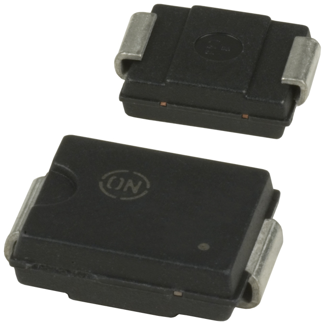
Littelfuse Inc. 的 1SMC36AT3G 是一款瞬态电压抑制二极管(TVS),属于高功率表面贴装器件,主要用于电路的过压保护。该型号额定击穿电压约为40V,适用于直流电源线和信号线路的浪涌保护。

其典型应用场景包括:工业控制设备、通信设备、消费类电子产品及汽车电子系统。在这些系统中,1SMC36AT3G可有效抑制因静电放电(ESD)、雷击感应、电感负载切换或电源突波等引起的瞬态过电压,防止敏感元器件损坏。

该器件采用SMC封装,具有较高的峰值脉冲功率(可达1500W),响应速度快(皮秒级),能迅速将过电压钳位于安全水平,保障后级电路稳定运行。常用于电源输入端口、接口电路(如USB、RS232)以及DC电源模块中,尤其适合空间受限但需高可靠保护的设计。

此外,1SMC36AT3G符合AEC-Q101车规认证,具备良好的可靠性和耐久性,因此也广泛应用于车载电子系统,如车身控制模块、车载充电器和照明系统等,提供稳定可靠的瞬态电压防护。
| 参数 | 数值 |
| 产品目录 | |
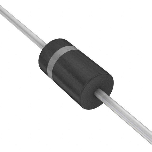
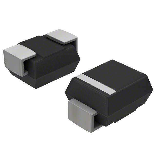
| 描述 | TVS DIODE 36VWM 58.1VC SMCTVS 二极管 - 瞬态电压抑制器 36V 1500W Unidirectional |
| 产品分类 | |
| 品牌 | ON Semiconductor |
| 产品手册 | |
| 产品图片 |
|
| rohs | 符合RoHS无铅 / 符合限制有害物质指令(RoHS)规范要求 |
| 产品系列 | 二极管与整流器,TVS二极管,TVS 二极管 - 瞬态电压抑制器,ON Semiconductor 1SMC36AT3G- |
| 数据手册 | |
| 产品型号 | 1SMC36AT3G |
| 不同频率时的电容 | - |
| 产品目录绘图 |
|
| 产品目录页面 | |
| 产品种类 | TVS 二极管 - 瞬态电压抑制器 |
| 供应商器件封装 | SMC |
| 其它名称 | 1SMC36AT3GOSDKR |
| 击穿电压 | 40 V |
| 功率-峰值脉冲 | 1500W (1.5kW) |
| 包装 | Digi-Reel® |
| 单向通道 | 1 |
| 双向通道 | - |
| 商标 | ON Semiconductor |
| 安装类型 | 表面贴装 |
| 安装风格 | SMD/SMT |
| 封装 | Reel |
| 封装/外壳 | DO-214AB,SMC |
| 封装/箱体 | DO-214AB |
| 尺寸 | 6.1 mm W x 7.11 mm L x 2.41 mm H |
| 峰值浪涌电流 | 25.8 A |
| 峰值脉冲功率耗散 | 1.5 kW |
| 工作温度 | -65°C ~ 150°C (TJ) |
| 工作电压 | 36 V |
| 工厂包装数量 | 2500 |
| 应用 | 通用 |
| 最大工作温度 | + 150 C |
| 最小工作温度 | - 65 C |
| 极性 | Unidirectional |
| 标准包装 | 1 |
| 电压-击穿(最小值) | 40V |
| 电压-反向关态(典型值) | 36V |
| 电压-箝位(最大值)@Ipp | 58.1V |
| 电流-峰值脉冲(10/1000µs) | - |
| 电源线路保护 | 无 |
| 端接类型 | SMD/SMT |
| 类型 | 齐纳 |
| 系列 | 1SMC5.0AT3G |
| 钳位电压 | 58.1 V |


- 商务部:美国ITC正式对集成电路等产品启动337调查
- 曝三星4nm工艺存在良率问题 高通将骁龙8 Gen1或转产台积电
- 太阳诱电将投资9.5亿元在常州建新厂生产MLCC 预计2023年完工
- 英特尔发布欧洲新工厂建设计划 深化IDM 2.0 战略
- 台积电先进制程称霸业界 有大客户加持明年业绩稳了
- 达到5530亿美元!SIA预计今年全球半导体销售额将创下新高
- 英特尔拟将自动驾驶子公司Mobileye上市 估值或超500亿美元
- 三星加码芯片和SET,合并消费电子和移动部门,撤换高东真等 CEO
- 三星电子宣布重大人事变动 还合并消费电子和移动部门
- 海关总署:前11个月进口集成电路产品价值2.52万亿元 增长14.8%


PDF Datasheet 数据手册内容提取
1SMC5.0AT3G Series, SZ1SMC5.0AT3G Series 1500 Watt Peak Power Zener Transient Voltage Suppressors .com Unidirectional* PLASTIC SURFACE MOUNT The SMC series is designed to protect voltage ZENER TRANSIENT sensitive components from high voltage, high energy transients. VOLTAGE SUPPRESSORS They have excellent clamping capability, high surge capability, 5.0−78 VOLTS low zener impedance and fast response time. The SMC series is 1500 WATT PEAK POWER supplied in Littelfuse exclusive, cost-effective, highly reliable package and is ideally suited for use in communication systems, automotive, numerical controls, process controls, medical equipment, business machines, power supplies and many other industrial/consumer applications. SMC CASE 403 PLASTIC Features • Working Peak Reverse Voltage Range − 5.0 V to 78 V • Standard Zener Breakdown Voltage Range − 6.7 V to 91.25 V • Peak Power − 1500 W @ 1 ms • MARKING DIAGRAM ESD Rating of Class 3 (>16 KV) per Human Body Model • Maximum Clamp Voltage @ Peak Pulse Current • Low Leakage < 5 A Above 10 V • UL 497B for Isolated Loop Circuit Protection • Maximum Temperature Coefficient Specified • Response Time is Typically < 1 ns • SZ Prefix for Automotive and Other Applications Requiring Unique • Site and Control Change Requirements; AEC−Q101 Qualified and PPAP Capable • Pb−Free Packages are Available Mechanical Characteristics: CASE: Void-free, transfer-molded, thermosetting plastic ORDERING INFORMATION FINISH: All external surfaces are corrosion resistant and leads are readily solderable Device Package Shipping MAXIMUM CASE TEMPERATURE FOR SOLDERING PURPOSES: 260ºC for 10 Seconds LEADS: Modified L−Bend providing more contact area to bond pads POLARITY: Cathode indicated by molded polarity bend MOUNTING POSITION: Any DEVICE MARKING INFORMATION Specifications subject to change without notice. © 2016 Littelfuse, Inc. 1 September 19, 2016 − Rev. 8 1SMC5.0AT3/D
1SMC5.0AT3G Series, SZ1SMC5.0AT3G Series MAXIMUM RATINGS Rating Symbol Value Unit Peak Power Dissipation (Note 1) @ TL = 25C, Pulse Width = 1 ms PPK 1500 W DC Power Dissipation @ TL = 75C PD 4.0 W Measured Zero Lead Length (Note 2) Derate Above 75C 54.6 mW/C Thermal Resistance from Junction−to−Lead R(cid:3)JL 18.3 C/W DC Power Dissipation (Note 3) @ TA = 25C PD 0.75 W Derate Above 25C 6.1 mW/C Thermal Resistance from Junction−to−Ambient R(cid:3)JA 165 C/W Forward Surge Current (Note 4) @ TA = 25C IFSM 200 A Operating and Storage Temperature Range TJ, Tstg −65 to +150 C Stresses exceeding Maximum Ratings may damage the device. Maximum Ratings are stress ratings only. Functional operation above the Recommended Operating Conditions is not implied. Extended exposure to stresses above the Recommended Operating Conditions may affect device reliability. 1. 10 x 1000 (cid:2)s, non−repetitive. 2. 1 in square copper pad, FR−4 board. 3. FR−4 board, using Littelfuse minimum recommended footprint, as shown in 403 case outline dimensions spec. 4. 1/2 sine wave (or equivalent square wave), PW = 8.3 ms, duty cycle = 4 pulses per minute maximum. ELECTRICAL CHARACTERISTICS (TA = 25C unless I otherwise noted, VF = 3.5 V Max @ IF = 100 A) (Note 5) IF Symbol Parameter IPP Maximum Reverse Peak Pulse Current VC Clamping Voltage @ IPP VRWM Working Peak Reverse Voltage VC VBRVRWM V IR VF IR Maximum Reverse Leakage Current @ VRWM IT VBR Breakdown Voltage @ IT IT Test Current IF Forward Current IPP VF Forward Voltage @ IF 5. 1/2 sine wave or equivalent, PW = 8.3 ms non−repetitive duty Uni−Directional TVS cycle Specifications subject to change without notice. © 2016 Littelfuse, Inc. 2 Publication Order Number: September 19, 2016 − Rev. 8 1SMC5.0AT3/D
1SMC5.0AT3G Series, SZ1SMC5.0AT3G Series ELECTRICAL CHARACTERISTICS (TA = 25C unless otherwise noted) Breakdown Voltage VC @ IPP (Note 8) VRWM Device (Note 6) IR @ VRWM VBR V (Note 7) @ IT VC IPP Device* Marking V (cid:2)A Min Nom Max mA V A 1SMC5.0AT3G GDE 5.0 1000 6.4 6.7 7.0 10 9.2 163 1SMC6.0AT3G GDG 6.0 1000 6.67 7.02 7.37 10 10.3 145.6 1SMC6.5AT3G GDK 6.5 500 7.22 7.6 7.98 10 11.2 133.9 1SMC7.5AT3G GDP 7.5 100 8.33 8.77 9.21 1 12.9 116.3 1SMC8.0AT3G GDR 8.0 50 8.89 9.36 9.83 1 13.6 110.3 1SMC9.0AT3G GDV 9.0 10 10 10.55 11.1 1 15.4 97.4 1SMC10AT3G GDX 10 5 11.1 11.7 12.3 1 17 88.2 1SMC12AT3G GEE 12 5 13.3 14 14.7 1 19.9 75.3 1SMC13AT3G GEG 13 5 14.4 15.15 15.9 1 21.5 69.7 1SMC14AT3G GEK 14 5 15.6 16.4 17.2 1 23.2 64.7 1SMC15AT3G GEM 15 5 16.7 17.6 18.5 1 24.4 61.5 1SMC16AT3G GEP 16 5 17.8 18.75 19.7 1 26 57.7 1SMC17AT3G GER 17 5 18.9 19.9 20.9 1 27.6 53.3 1SMC18AT3G GET 18 5 20 21.05 22.1 1 29.2 51.4 1SMC20AT3G GEV 20 5 22.2 23.35 24.5 1 32.4 46.3 1SMC22AT3G GEX 22 5 24.4 25.65 26.9 1 35.5 42.2 1SMC24AT3G GEZ 24 5 26.7 28.1 29.5 1 38.9 38.6 1SMC26AT3G GFE 26 5 28.9 30.4 31.9 1 42.1 35.6 1SMC28AT3G GFG 28 5 31.1 32.75 34.4 1 45.4 33 1SMC30AT3G GFK 30 5 33.3 35.05 36.8 1 48.4 31 1SMC33AT3G GFM 33 5 36.7 38.65 40.6 1 53.3 28.1 1SMC36AT3G GFP 36 5 40 42.1 44.2 1 58.1 25.8 1SMC40AT3G GFR 40 5 44.4 46.75 49.1 1 64.5 32.2 1SMC43AT3G GFT 43 5 47.8 50.3 52.8 1 69.4 21.6 1SMC48AT3G GFX 48 5 53.3 56.1 58.9 1 77.4 19.4 1SMC51AT3G GFZ 51 5 56.7 59.7 62.7 1 82.4 18.2 1SMC54AT3G GGE 54 5 60 63.15 66.3 1 87.1 17.2 1SMC58AT3G GGG 58 5 64.4 67.8 71.2 1 93.6 16 1SMC60AT3G GGK 60 5 66.7 70.2 73.7 1 96.8 15.5 1SMC64AT3G GGM 64 5 71.1 74.85 78.6 1 103 14.6 1SMC70AT3G GGP 70 5 77.8 81.9 86 1 113 13.3 1SMC75AT3G GGR 75 5 83.3 87.7 92.1 1 121 12.4 1SMC78AT3G GGT 78 5 86.7 91.25 95.8 1 126 11.4 6. A transient suppressor is normally selected according to the maximum working peak reverse voltage (VRWM), which should be equal to or greater than the DC or continuous peak operating voltage level. 7. VBR measured at pulse test current IT at an ambient temperature of 25C. 8. Surge current waveform per Figure 2 and derate per Figure 3 of the General Data − 1500 Watt at the beginning of this group. *Include SZ-prefix devices where applicable. Specifications subject to change without notice. © 2016 Littelfuse, Inc. 3 Publication Order Number: September 19, 2016 − Rev. 8 1SMC5.0AT3/D
1SMC5.0AT3G Series, SZ1SMC5.0AT3G Series 100 PULSE WIDTH (tP) IS DEFINED NPUOLNSREE WPEATVIETFIVOERM tr(cid:2) 10 (cid:2)s ACSU RTRHEANT TP ODEINCTA WYSH ETORE 5 0T%HE PEAK kW) SHOWN IN FIGURE 2 100 OF IPP. R ( PEAK VALUE - IPP WE %) K PO 10 ALUE ( HALF VALUE - IPP A V 2 E 50 P , k p P tP 1 0 0.1 (cid:2)s 1 (cid:2)s 10 (cid:2)s 100 (cid:2)s 1 ms 10 ms 0 1 2 3 4 tP, PULSE WIDTH t, TIME (ms) Figure 1. Pulse Rating Curve Figure 2. Pulse Waveform 160 C 1000 LSE DERATING IN % OFR OR CURRENT @ T= 25A 1118602400000 CURRENT (AMPS)5215200000000 tTPL(cid:2)(cid:2)==(cid:2)(cid:2)1205(cid:2)(cid:2)Cs VBR(cid:2)(N2O02(cid:2)MV4)(cid:2)V(cid:2)=(cid:2)6.8(cid:2)TO43(cid:2)1(cid:2)V37(cid:2)1V518(cid:2)20V0(cid:2)V(cid:2)V PEAK PUAK POWE 4200 , TEST T 150 E I 2 P 0 1 0 25 50 75 100 125 150 0.3 0.5 0.7 1 2 3 5 7 10 20 30 TA, AMBIENT TEMPERATURE (C) (cid:4)VBR, INSTANTANEOUS INCREASE IN VBR ABOVE VBR (NOM) (VOLTS) Figure 3. Pulse Derating Curve Figure 4. Dynamic Impedance UL RECOGNITION The entire series has Underwriters Laboratory including Strike Voltage Breakdown test, Endurance Recognition for the classification of protectors (QVGQ2) Conditioning, Temperature test, Dielectric Voltage-Withstand under the UL standard for safety 497B and File #E128662. test, Discharge test and several more. Many competitors only have one or two devices recognized Whereas, some competitors have only passed a or have recognition in a non-protective category. Some flammability test for the package material, we have been competitors have no recognition at all. With the UL497B recognized for much more to be included in their Protector recognition, our parts successfully passed several tests category. Specifications subject to change without notice. © 2016 Littelfuse, Inc. 4 Publication Order Number: September 19, 2016 − Rev. 8 1SMC5.0AT3/D
1SMC5.0AT3G Series, SZ1SMC5.0AT3G Series APPLICATION NOTES Response Time minimum lead lengths and placing the suppressor device as In most applications, the transient suppressor device is close as possible to the equipment or components to be placed in parallel with the equipment or component to be protected will minimize this overshoot. protected. In this situation, there is a time delay associated Some input impedance represented by Z is essential to in with the capacitance of the device and an overshoot prevent overstress of the protection device. This impedance condition associated with the inductance of the device and should be as high as possible, without restricting the circuit the inductance of the connection method. The capacitive operation. effect is of minor importance in the parallel protection scheme because it only produces a time delay in the Duty Cycle Derating transition from the operating voltage to the clamp voltage as The data of Figure 1 applies for non-repetitive conditions shown in Figure 5. and at a lead temperature of 25C. If the duty cycle increases, The inductive effects in the device are due to actual the peak power must be reduced as indicated by the curves turn-on time (time required for the device to go from zero of Figure 7. Average power must be derated as the lead or current to full current) and lead inductance. This inductive ambient temperature rises above 25C. The average power effect produces an overshoot in the voltage across the derating curve normally given on data sheets may be equipment or component being protected as shown in normalized and used for this purpose. Figure 6. Minimizing this overshoot is very important in the At first glance the derating curves of Figure 7 appear to be application, since the main purpose for adding a transient in error as the 10 ms pulse has a higher derating factor than suppressor is to clamp voltage spikes. The SMC series have the 10 (cid:2)s pulse. However, when the derating factor for a a very good response time, typically < 1 ns and negligible given pulse of Figure 7 is multiplied by the peak power value inductance. However, external inductive effects could of Figure 1 for the same pulse, the results follow the produce unacceptable overshoot. Proper circuit layout, expected trend. Specifications subject to change without notice. © 2016 Littelfuse, Inc. 6 Publication Order Number: September 19, 2016 − Rev. 8 1SMC5.0AT3/D
1SMC5.0AT3G Series, SZ1SMC5.0AT3G Series TYPICAL PROTECTION CIRCUIT Zin Vin LOAD VL Vin (TRANSIENT) OVERSHOOT DUE TO V Vin (TRANSIENT) V INDUCTIVE EFFECTS VL VL Vin td tD = TIME DELAY DUE TO CAPACITIVE EFFECT t t Figure 5. Figure 6. 1 0.7 0.5 R 0.3 O CT 0.2 A PULSE WIDTH F G 0.1 10 ms N TI 0.07 A R 0.05 E 1 ms D 0.03 0.02 100 (cid:2)s 10 (cid:2)s 0.01 0.1 0.2 0.5 1 2 5 10 20 50 100 D, DUTY CYCLE (%) Figure 7. Typical Derating Factor for Duty Cycle Specifications subject to change without notice. © 2016 Littelfuse, Inc. 6 Publication Order Number: September 19, 2016 − Rev. 8 1SMC5.0AT3/D
1SMC5.0AT3G Series, SZ1SMC5.0AT3G Series PACKAGE DIMENSIONS SMC HE NO1.TEDSI:MENSIONING AND TOLERANCING PER ANSI Y14.5M, 1982. 2. CONTROLLING DIMENSION: INCH. E 3. D DIMENSION SHALL BE MEASURED WITHIN DIMENSION P. 4. 403-01 THRU -02 OBSOLETE, NEW STANDARD 403-03. MILLIMETERS INCHES DIM MIN NOM MAX MIN NOM MAX A b D A1 b c D E HE L L1 A c A1 L L1 SOLDERING FOOTPRINT mm inches Information furnished is believed to be accurate and reliable. However, users should independently evaluate the suitability of and test each product selected for their own applications. Littelfuse products are not designed for, and shall not be used for, any purpose (including, without limitation, military, aerospace, medical, life-saving, life-sustaining or nuclear facility applications, devices intended for surgical implant into the body, or any other application in which the failure or lack of desired operation of the product may result in personal injury, death, or property damage) other than those expressly set forth in applicable Littelfuse product documentation. Warranties granted by Littelfuse shall be deemed void for products used for any purpose not expressly set forth in applicable Littelfuse documentation. Littelfuse shall not be liable for any claims or damages arising out of products used in applications not expressly intended by Littelfuse as set forth in applicable Littelfuse documentation. The sale and use of Littelfuse products is subject to Littelfuse Terms and Conditions of Sale, unless otherwise agreed by Littelfuse. .com Specifications subject to change without notice. © 2016 Littelfuse, Inc. September 19, 2016 − Rev. 8 1SMC5.0AT3/D