ICGOO在线商城 > 分立半导体产品 > 二极管 - 齐纳 - 单 > 1PMT5927BT1G
 Datasheet下载
- 型号: 1PMT5927BT1G
- 制造商: ON Semiconductor
- 库位|库存: xxxx|xxxx
- 要求:
| 数量阶梯 | 香港交货 | 国内含税 |
| +xxxx | $xxxx | ¥xxxx |
查看当月历史价格
查看今年历史价格
1PMT5927BT1G产品简介:
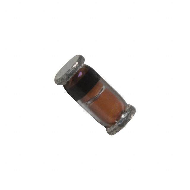
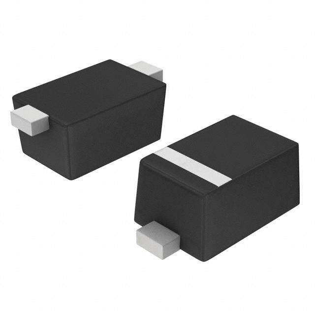
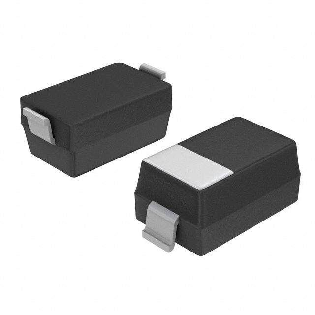
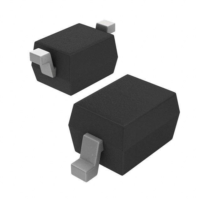
ICGOO电子元器件商城为您提供1PMT5927BT1G由ON Semiconductor设计生产,在icgoo商城现货销售,并且可以通过原厂、代理商等渠道进行代购。 1PMT5927BT1G价格参考。ON Semiconductor1PMT5927BT1G封装/规格:二极管 - 齐纳 - 单, Zener Diode 12V 3.2W ±5% 表面贴装 Powermite。您可以下载1PMT5927BT1G参考资料、Datasheet数据手册功能说明书,资料中有1PMT5927BT1G 详细功能的应用电路图电压和使用方法及教程。
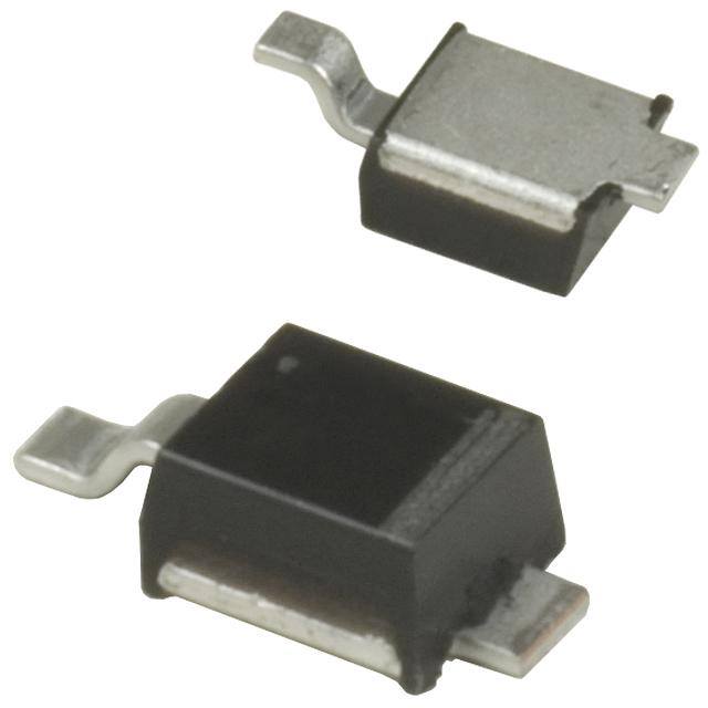
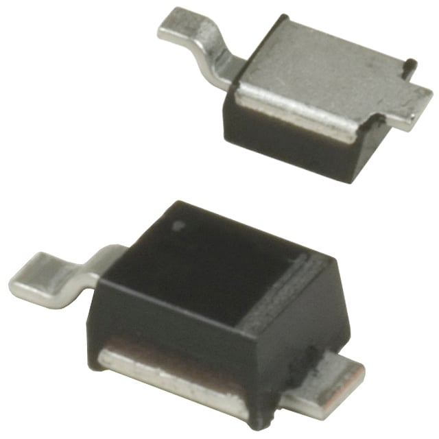
ON Semiconductor生产的1PMT5927BT1G是一款齐纳二极管,属于单齐纳二极管类别。该器件采用SOD-523小型表面贴装封装,具有低功耗、高稳定性和快速响应的特点,适用于对空间和能效要求较高的电子电路。

1PMT5927BT1G的标称齐纳电压为2.7V,容差控制精密,适合用于低电压稳压和参考电压源设计。其主要应用场景包括:便携式电子产品(如智能手机、平板电脑、可穿戴设备)中的电源管理电路,用于保护敏感元件免受电压波动影响;在电池供电系统中提供稳定的基准电压或实现过压保护;也可用于接口电路中进行ESD(静电放电)保护和电压钳位,提升系统可靠性。

此外,该器件符合RoHS环保要求,并具备良好的温度稳定性,可在较宽的工作温度范围内保持性能一致,因此也广泛应用于消费类电子、工业控制、通信模块及汽车电子中的辅助电路中。由于其小型化封装,特别适合高密度PCB布局,有助于缩小整体产品体积。

总之,1PMT5927BT1G凭借其稳定可靠的电气性能和紧凑的封装,是现代电子设备中理想的电压参考与保护元件。
| 参数 | 数值 |
| 产品目录 | |
| 描述 | DIODE ZENER 12V 3.2W POWERMITE稳压二极管 12V 3.2W Powermite |
| 产品分类 | 单二极管/齐纳分离式半导体 |
| 品牌 | ON Semiconductor |
| 产品手册 | |
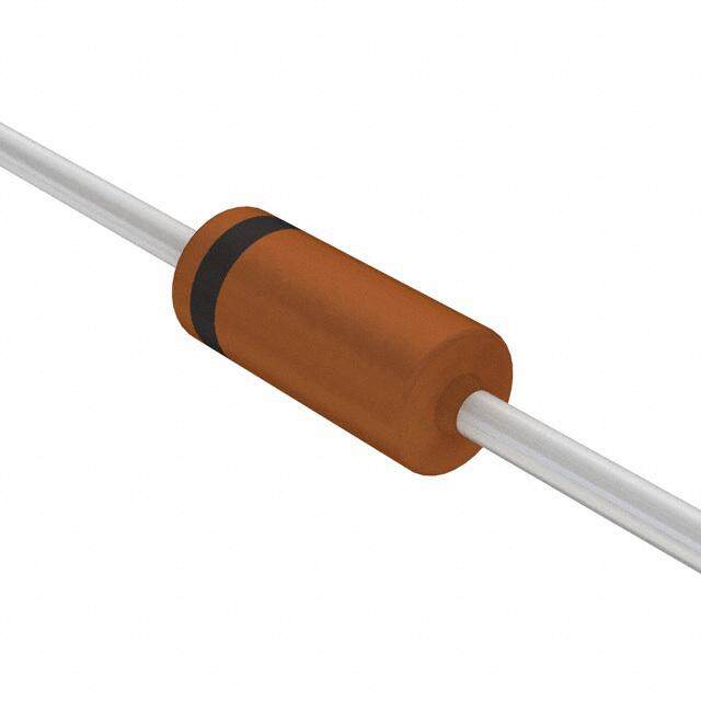
| 产品图片 |
|
| rohs | 符合RoHS无铅 / 符合限制有害物质指令(RoHS)规范要求 |
| 产品系列 | 二极管与整流器,稳压二极管,ON Semiconductor 1PMT5927BT1G- |
| 数据手册 | |
| 产品型号 | 1PMT5927BT1G |
| 不同If时的电压-正向(Vf) | 1.25V @ 200mA |
| 不同 Vr时的电流-反向漏电流 | 1µA @ 9.1V |
| 产品种类 | |
| 供应商器件封装 | Powermite |
| 其它名称 | 1PMT5927BT1GOS |
| 功率-最大值 | 3.2W |
| 功率耗散 | 500 mW |
| 包装 | 带卷 (TR) |
| 商标 | ON Semiconductor |
| 安装类型 | 表面贴装 |
| 安装风格 | SMD/SMT |
| 容差 | ±5% |
| 封装 | Reel |
| 封装/外壳 | DO-216AA |
| 封装/箱体 | DO-216AA |
| 工作温度 | -55°C ~ 150°C |
| 工厂包装数量 | 3000 |
| 最大反向漏泄电流 | 1 uA |
| 最大工作温度 | + 150 C |
| 最大齐纳阻抗 | 6.5 Ohms |
| 最小工作温度 | - 55 C |
| 标准包装 | 3,000 |
| 电压-齐纳(标称值)(Vz) | 12V |
| 电压容差 | 5 % |
| 系列 | 1PMT5927B |
| 配置 | Single |
| 阻抗(最大值)(Zzt) | 6.5 欧姆 |
| 齐纳电压 | 12 V |
| 齐纳电流 | 200 mA |


- 商务部:美国ITC正式对集成电路等产品启动337调查
- 曝三星4nm工艺存在良率问题 高通将骁龙8 Gen1或转产台积电
- 太阳诱电将投资9.5亿元在常州建新厂生产MLCC 预计2023年完工
- 英特尔发布欧洲新工厂建设计划 深化IDM 2.0 战略
- 台积电先进制程称霸业界 有大客户加持明年业绩稳了
- 达到5530亿美元!SIA预计今年全球半导体销售额将创下新高
- 英特尔拟将自动驾驶子公司Mobileye上市 估值或超500亿美元
- 三星加码芯片和SET,合并消费电子和移动部门,撤换高东真等 CEO
- 三星电子宣布重大人事变动 还合并消费电子和移动部门
- 海关总署:前11个月进口集成电路产品价值2.52万亿元 增长14.8%


PDF Datasheet 数据手册内容提取
1PMT5920B Series 3.2 Watt Plastic Surface Mount ® POWERMITE Package This complete new line of 3.2 Watt Zener Diodes are offered in highly efficient micro miniature, space saving surface mount with its www.onsemi.com unique heat sink design. The POWERMITE package has the same thermal performance as the SMA while being 50% smaller in PLASTIC SURFACE MOUNT footprint area and delivering one of the lowest height profiles (1.1 mm) in the industry. Because of its small size, it is ideal for use 3.2 WATT ZENER DIODES in cellular phones, portable devices, business machines and many 6.2 − 47 VOLTS other industrial/consumer applications. Features • 1 2 Zener Breakdown Voltage: 6.2 − 47 V • DC Power Dissipation: 3.2 W with Tab 1 (Cathode) @ 75°C 1: CATHODE • Low Leakage < 5 (cid:2)A 2: ANODE • ESD Rating of Class 3 (> 16 kV) per Human Body Model • Low Profile − Maximum Height of 1.1 mm 1 • Integral Heat Sink/Locking Tabs • Full Metallic Bottom Eliminates Flux Entrapment 2 • Small Footprint − Footprint Area of 8.45 mm2 POWERMITE • Supplied in 12 mm Tape and Reel CASE 457 • Lead Orientation in Tape: Cathode (Short) Lead to Sprocket Holes • POWERMITE is JEDEC Registered as DO−216AA • MARKING DIAGRAM Cathode Indicated by Polarity Band • These Devices are Pb−Free and are RoHS Compliant M Mechanical Characteristics 1 xxB (cid:2) 2 CATHODE ANODE CASE: Void-free, transfer-molded, thermosetting plastic FINISH: All external surfaces are corrosion resistant and leads are M = Date Code readily solderable xxB = Specific Device Code MOUNTING POSITION: Any (See Table on Page 2) MAXIMUM CASE TEMPERATURE FOR SOLDERING PURPOSES: (cid:2) = Pb−Free Package 260°C for 10 Seconds ORDERING INFORMATION Device Package Shipping† 1PMT59xxBT1G POWERMITE 3000 / Tape & (Pb−Free) Reel †For information on tape and reel specifications, including part orientation and tape sizes, please refer to our Tape and Reel Packaging Specifications Brochure, BRD8011/D. © Semiconductor Components Industries, LLC, 2007 1 Publication Order Number: December, 2018 − Rev. 5 1PMT5920B/D
1PMT5920B Series MAXIMUM RATINGS Rating Symbol Value Unit DC Power Dissipation @ TA = 25°C (Note 1) °PD° 500 °mW Derate above 25°C 4.0 mW/°C Thermal Resistance, Junction−to−Ambient R(cid:3)JA 248 °C/W Thermal Resistance, Junction−to−Lead (Anode) R(cid:3)Janode 35 °C/W Maximum DC Power Dissipation (Note 2) °PD° 3.2 W Thermal Resistance from Junction−to−Tab (Cathode) R(cid:3)Jcathode 23 °C/W Operating and Storage Temperature Range TJ, Tstg −55 to +150 °C Stresses exceeding those listed in the Maximum Ratings table may damage the device. If any of these limits are exceeded, device functionality should not be assumed, damage may occur and reliability may be affected. 1. Mounted with recommended minimum pad size, PC board FR−4. 2. At Tab (Cathode) temperature, Ttab = 75°C ELECTRICAL CHARACTERISTICS (TL = 25°C unless I otherwise noted, VF = 1.5 V Max. @ IF = 200 mAdc for all types) IF Symbol Parameter VZ Reverse Zener Voltage @ IZT IZT Reverse Current ZZT Maximum Zener Impedance @ IZT VZ VR V IZK Reverse Current IIRZTVF ZZK Maximum Zener Impedance @ IZK IR Reverse Leakage Current @ VR VR Reverse Voltage IF Forward Current Zener Voltage Regulator VF Forward Voltage @ IF ELECTRICAL CHARACTERISTICS (TL = 30°C unless otherwise noted, VF = 1.25 Volts @ 200 mA) Zener Voltage (Note 3) ZZT @ IZT ZZK @ IZK Device VZ @ IZT (Volts) IZT IR @ VR VR (Note 4) (Note 4) IZK Device* Marking Min Nom Max (mA) ((cid:2)A) (V) ((cid:3)) ((cid:3)) (mA) 1PMT5920BT1G 20B 5.89 6.2 6.51 60.5 5.0 4.0 2.0 200 1.0 1PMT5921BT1G 21B 6.46 6.8 7.14 55.1 5.0 5.2 2.5 200 1.0 1PMT5924BT1G 24B 8.64 9.1 9.56 41.2 5.0 7.0 4.0 500 0.5 1PMT5927BT1G 27B 11.4 12 12.6 31.2 1.0 9.1 6.5 550 0.25 1PMT5929BT1G 29B 14.25 15 15.75 25 1.0 11.4 9.0 600 0.25 1PMT5933BT1G 33B 20.9 22 23.1 17 1.0 16.7 17.5 650 0.25 1PMT5934BT1G 34B 22.8 24 25.2 15.6 1.0 18.2 19 700 0.25 1PMT5935BT1G 35B 25.65 27 28.35 13.9 1.0 20.6 23 700 0.25 1PMT5941BT1G 41B 44.65 47 49.35 8.0 1.0 35.8 67 1000 0.25 Product parametric performance is indicated in the Electrical Characteristics for the listed test conditions, unless otherwise noted. Product performance may not be indicated by the Electrical Characteristics if operated under different conditions. 3. Zener voltage is measured with the device junction in thermal equilibrium with an ambient temperature of 25°C. 4. Zener Impedance Derivation ZZT and ZZK are measured by dividing the AC voltage drop across the device by the AC current applied. The specified limits are for IZ(ac) = 0.1 IZ(dc) with the ac frequency = 60 Hz. www.onsemi.com 2
1PMT5920B Series TYPICAL CHARACTERISTICS W)3.5 100 N ( ATIO 3 mA) DISSIP2.5 RENT ( 10 R 2 R WE TL CU O1.5 R P E UM 1 ZEN 1 XIM I, Z A0.5 M P , D 025 50 75 100 125 150 175 0.15 6 7 8 9 10 11 T, TEMPERATURE (°C) VZ, ZENER VOLTAGE (VOLTS) Figure 1. Steady State Power Derating Figure 2. V to 10 Volts Z 100 °C)10 V/ 50 m A) 30 NT ( 8 VZ @ IZT m 20 E NT ( 10 FICI 6 E F R 5 E 4 R O U 3 C R C 2 RE 2 NE 1 TU I , ZEZ 00..53 MPERA−20 0.2 E T 0.1 , Z−4 0 10 20 30 40 50 60 70 80 90 100 V 2 4 6 8 10 12 (cid:3) VZ, ZENER VOLTAGE (VOLTS) VZ, ZENER VOLTAGE (VOLTS) Figure 4. Zener Voltage − To 12 Volts Figure 3. V = 12 thru 47 Volts Z C) ° 200 200 mV/ MS) IZ(dc) = 1mA NT ( VZ @ IZT OH100 CIE100 CE ( 7500 FI 70 N F A E D 30 O 50 E C P 20 E M UR 30 C I T MI 10 10 mA MPERA 20 DYNA 75 , TEZ 10 Z , Z 32 20 mA iZ(rms) = 0.1 IZ(dc) (cid:3)V 10 20 30 50 70 100 200 5 7 10 20 30 50 70 100 VZ, ZENER VOLTAGE (VOLTS) VZ, ZENER VOLTAGE (VOLTS) Figure 5. Zener Voltage − 14 To 47 Volts Figure 6. Effect of Zener Voltage www.onsemi.com 3
1PMT5920B Series TYPICAL CHARACTERISTICS 1 k MS) 500 TJ = 25°C OH iZ(rms) = 0.1 IZ(dc) E ( 200 C N 100 A D 50 E P M 20 C I MI 10 A N 5 22 V Y D Z , Z 2 12 V6.8 V 1 0.5 1 2 5 10 20 50 100 200 500 IZ, ZENER TEST CURRENT (mA) Figure 7. Effect of Zener Current 10,000 F) p E (1000 C N MEASURED @ 0 V BIAS A T CI PA MEASURED @ 50% VR A 100 C C, 10 1 10 100 VZ, REVERSE ZENER VOLTAGE (VOLTS) Figure 8. Capacitance versus Reverse Zener Voltage www.onsemi.com 4
1PMT5920B Series PACKAGE DIMENSIONS (cid:2) POWERMITE CASE 457−04 ISSUE F NOTES: −A− C F 1. DIMENSIONING AND TOLERANCING PER ANSI Y14.5M, 1982. J 0.08 (0.003) M T B S C S 2. CONTROLLING DIMENSION: MILLIMETER. 3. DIMENSIONS A AND B DO NOT INCLUDE MOLD FLASH, PROTRUSIONS OR GATE BURRS. MOLD S FLASH, PROTRUSIONS OR GATE BURRS SHALL NOT EXCEED 0.15 (0.006) PER SIDE. MILLIMETERS INCHES PIN 1 DIM MIN MAX MIN MAX −B− A 1.75 2.05 0.069 0.081 B 1.75 2.18 0.069 0.086 K C 0.85 1.15 0.033 0.045 D 0.40 0.69 0.016 0.027 PIN 2 F 0.70 1.00 0.028 0.039 H -0.05 +0.10 -0.002 +0.004 J 0.10 0.25 0.004 0.010 R K 3.60 3.90 0.142 0.154 L L 0.50 0.80 0.020 0.031 R 1.20 1.50 0.047 0.059 S 0.50 REF 0.019 REF J H D 0.08 (0.003) M T B S C S −T− SOLDERING FOOTPRINT* 0.635 0.025 2.67 0.105 0.762 0.030 2.54 1.27 0.100 0.050 (cid:2) (cid:3) mm SCALE 10:1 inches *For additional information on our Pb−Free strategy and soldering details, please download the ON Semiconductor Soldering and Mounting Techniques Reference Manual, SOLDERRM/D. POWERMITE is a registered trademark of and used under a license from Microsemi Corporation. ON Semiconductor and are trademarks of Semiconductor Components Industries, LLC dba ON Semiconductor or its subsidiaries in the United States and/or other countries. ON Semiconductor owns the rights to a number of patents, trademarks, copyrights, trade secrets, and other intellectual property. A listing of ON Semiconductor’s product/patent coverage may be accessed at www.onsemi.com/site/pdf/Patent−Marking.pdf. ON Semiconductor reserves the right to make changes without further notice to any products herein. ON Semiconductor makes no warranty, representation or guarantee regarding the suitability of its products for any particular purpose, nor does ON Semiconductor assume any liability arising out of the application or use of any product or circuit, and specifically disclaims any and all liability, including without limitation special, consequential or incidental damages. Buyer is responsible for its products and applications using ON Semiconductor products, including compliance with all laws, regulations and safety requirements or standards, regardless of any support or applications information provided by ON Semiconductor. “Typical” parameters which may be provided in ON Semiconductor data sheets and/or specifications can and do vary in different applications and actual performance may vary over time. All operating parameters, including “Typicals” must be validated for each customer application by customer’s technical experts. ON Semiconductor does not convey any license under its patent rights nor the rights of others. ON Semiconductor products are not designed, intended, or authorized for use as a critical component in life support systems or any FDA Class 3 medical devices or medical devices with a same or similar classification in a foreign jurisdiction or any devices intended for implantation in the human body. Should Buyer purchase or use ON Semiconductor products for any such unintended or unauthorized application, Buyer shall indemnify and hold ON Semiconductor and its officers, employees, subsidiaries, affiliates, and distributors harmless against all claims, costs, damages, and expenses, and reasonable attorney fees arising out of, directly or indirectly, any claim of personal injury or death associated with such unintended or unauthorized use, even if such claim alleges that ON Semiconductor was negligent regarding the design or manufacture of the part. ON Semiconductor is an Equal Opportunity/Affirmative Action Employer. This literature is subject to all applicable copyright laws and is not for resale in any manner. PUBLICATION ORDERING INFORMATION LITERATURE FULFILLMENT: N. American Technical Support: 800−282−9855 Toll Free ON Semiconductor Website: www.onsemi.com Literature Distribution Center for ON Semiconductor USA/Canada 19521 E. 32nd Pkwy, Aurora, Colorado 80011 USA Europe, Middle East and Africa Technical Support: Order Literature: http://www.onsemi.com/orderlit Phone: 303−675−2175 or 800−344−3860 Toll Free USA/Canada Phone: 421 33 790 2910 Fax: 303−675−2176 or 800−344−3867 Toll Free USA/Canada For additional information, please contact your local Email: orderlit@onsemi.com Sales Representative ◊ www.onsemi.com 1PMT5920B/D 5