ICGOO在线商城 > 分立半导体产品 > 二极管 - 齐纳 - 单 > 1N5921BRLG
 Datasheet下载
- 型号: 1N5921BRLG
- 制造商: ON Semiconductor
- 库位|库存: xxxx|xxxx
- 要求:
| 数量阶梯 | 香港交货 | 国内含税 |
| +xxxx | $xxxx | ¥xxxx |
查看当月历史价格
查看今年历史价格
1N5921BRLG产品简介:
ICGOO电子元器件商城为您提供1N5921BRLG由ON Semiconductor设计生产,在icgoo商城现货销售,并且可以通过原厂、代理商等渠道进行代购。 1N5921BRLG价格参考¥0.57-¥1.13。ON Semiconductor1N5921BRLG封装/规格:二极管 - 齐纳 - 单, Zener Diode 6.8V 3W ±5% Through Hole Axial。您可以下载1N5921BRLG参考资料、Datasheet数据手册功能说明书,资料中有1N5921BRLG 详细功能的应用电路图电压和使用方法及教程。
型号为1N5921BRLG的齐纳二极管属于安森美半导体(ON Semiconductor)的产品,属于单齐纳二极管。该器件主要用于电压参考和稳压应用。

其主要应用场景包括:

1. 电源电路:用于提供稳定的参考电压,确保输出电压在负载变化时保持恒定。
2. 过压保护电路:作为电压钳位元件,防止瞬态高压对后续电路造成损害。
3. 基准电压源:在模拟电路、ADC/DAC电路中提供精确的电压基准点。
4. 工业控制系统:用于传感器信号调理、仪表放大器参考电压等场合。
5. 消费类电子产品:如充电器、适配器等小型电源设备中的稳压控制。

该器件采用表面贴装封装(如DO-214AC),适合自动化生产,具有良好的稳定性和可靠性,适用于中低功率应用场景。
| 参数 | 数值 |
| 产品目录 | |
| 描述 | DIODE ZENER 6.8V 3W AXIAL稳压二极管 6.8V 3W |
| 产品分类 | 单二极管/齐纳分离式半导体 |
| 品牌 | ON Semiconductor |
| 产品手册 | |
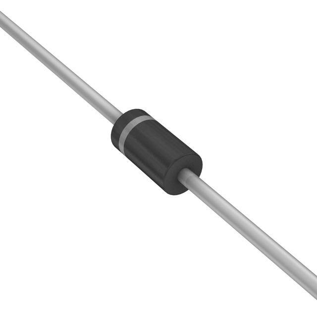
| 产品图片 |
|
| rohs | 符合RoHS无铅 / 符合限制有害物质指令(RoHS)规范要求 |
| 产品系列 | 二极管与整流器,稳压二极管,ON Semiconductor 1N5921BRLG- |
| 数据手册 | |
| 产品型号 | 1N5921BRLG |
| PCN设计/规格 | |
| 不同If时的电压-正向(Vf) | 1.5V @ 200mA |
| 不同 Vr时的电流-反向漏电流 | 5µA @ 5.2V |
| 产品种类 | |
| 供应商器件封装 | 轴向 |
| 其它名称 | 1N5921BRLGOSCT |
| 功率-最大值 | 3W |
| 功率耗散 | 3 W |
| 包装 | 剪切带 (CT) |
| 商标 | ON Semiconductor |
| 安装类型 | 通孔 |
| 安装风格 | Through Hole |
| 容差 | ±5% |
| 封装 | Reel |
| 封装/外壳 | DO-204AL,DO-41,轴向 |
| 封装/箱体 | DO-41 |
| 工作温度 | -65°C ~ 200°C |
| 工厂包装数量 | 6000 |
| 最大反向漏泄电流 | 5 uA |
| 最大工作温度 | + 200 C |
| 最大齐纳阻抗 | 2.5 Ohms |
| 最小工作温度 | - 65 C |
| 标准包装 | 1 |
| 电压-齐纳(标称值)(Vz) | 6.8V |
| 电压容差 | 5 % |
| 系列 | 1N5921B |
| 配置 | Single |
| 阻抗(最大值)(Zzt) | 2.5 欧姆 |
| 齐纳电压 | 6.8 V |
| 齐纳电流 | 220 mA |


- 商务部:美国ITC正式对集成电路等产品启动337调查
- 曝三星4nm工艺存在良率问题 高通将骁龙8 Gen1或转产台积电
- 太阳诱电将投资9.5亿元在常州建新厂生产MLCC 预计2023年完工
- 英特尔发布欧洲新工厂建设计划 深化IDM 2.0 战略
- 台积电先进制程称霸业界 有大客户加持明年业绩稳了
- 达到5530亿美元!SIA预计今年全球半导体销售额将创下新高
- 英特尔拟将自动驾驶子公司Mobileye上市 估值或超500亿美元
- 三星加码芯片和SET,合并消费电子和移动部门,撤换高东真等 CEO
- 三星电子宣布重大人事变动 还合并消费电子和移动部门
- 海关总署:前11个月进口集成电路产品价值2.52万亿元 增长14.8%


PDF Datasheet 数据手册内容提取
1N5913B Series 3 W DO-41 Surmetic 30 Zener Voltage Regulators This is a complete series of 3 W Zener diodes with limits and excellentoperatingcharacteristicsthatreflectthesuperiorcapabilities of silicon-oxide passivated junctions. All this in an axial-lead, www.onsemi.com transfer-moldedplasticpackagethatoffersprotectioninallcommon environmentalconditions. Features Cathode Anode ZenerVoltageRange- 3.3Vto200V ESDRatingofClass3(>16KV)perHumanBodyModel SurgeRatingof98W@1ms MaximumLimitsGuaranteedonuptoSixElectricalParameters PackageNoLargerthantheConventional1WPackage AXIALLEAD CASE59 Pb-FreePackagesareAvailable PLASTIC STYLE1 MechanicalCharacteristics CASE:Voidfree,transfer-molded,thermosettingplastic MARKINGDIAGRAM FINISH:Allexternalsurfacesarecorrosionresistantandleadsare readilysolderable A MAXIMUMLEADTEMPERATUREFORSOLDERINGPURPOSES: 1N 260C,1/16fromthecasefor10seconds 59xxB YYWWG POLARITY:Cathodeindicatedbypolarityband G MOUNTINGPOSITION:Any A =AssemblyLocation 1N59xxB =DeviceNumber MAXIMUMRATINGS YY =Year Rating Symbol Value Unit WW =WorkWeek G =Pb-FreePackage Max.SteadyStatePowerDissipation PD 3 W (Note:Microdotmaybeineitherlocation) @TL=75C,LeadLength=3/8 Derateabove75C 24 mW/C ORDERINGINFORMATION SteadyStatePowerDissipation PD 1 W @TA=50C Device Package Shipping† Derateabove50C 6.67 mW/C 1N59xxB,G AxialLead 2000Units/Box OperatingandStorage TJ,Tstg -65to C (Pb-Free) TemperatureRange +200 1N59xxBRL,G AxialLead 6000/Tape&Reel StressesexceedingthoselistedintheMaximumRatingstablemaydamagethe (Pb-Free) device.Ifanyoftheselimitsareexceeded,devicefunctionalityshouldnotbe assumed,damagemayoccurandreliabilitymaybeaffected. †Forinformationontapeandreelspecifications, includingpartorientationandtapesizes,please refertoourTapeandReelPackagingSpecification Brochure,BRD8011/D. *ForadditionalinformationonourPb-Freestrategyandsolderingdetails,please download the ON Semiconductor Soldering and Mounting Techniques ReferenceManual,SOLDERRM/D. SemiconductorComponentsIndustries,LLC,2006 1 PublicationOrderNumber: December,2019- Rev.7 1N5913B/D
1N5913B Series ELECTRICALCHARACTERISTICS I (TL=30Cunlessotherwisenoted, VF=1.5VMax@IF=200mAdcforalltypes) IF Symbol Parameter VZ ReverseZenerVoltage@IZT IZT ReverseCurrent ZZT MaximumZenerImpedance@IZT VZVR V IR VF IZK ReverseCurrent IZT ZZK MaximumZenerImpedance@IZK IR ReverseLeakageCurrent@VR VR BreakdownVoltage IF ForwardCurrent VF ForwardVoltage@IF ZenerVoltageRegulator IZM MaximumDCZenerCurrent www.onsemi.com 2
1N5913B Series ELECTRICALCHARACTERISTICS(TL=30Cunlessotherwisenoted,VF=1.5VMax@IF=200mAdcforalltypes) ZenerVoltage(Note2) ZenerImpedance(Note3) LeakageCurrent Device† Device VZ(Volts) @IZT ZZT@IZT ZZK@IZK IR@VR IZM (Note1) Marking Min Nom Max mA Ω Ω mA mAMax Volts mA 1N5913B,G 1N5913B 3.14 3.3 3.47 113.6 10 500 1 100 1 454 1N5917B,G 1N5917B 4.47 4.7 4.94 79.8 5 500 1 5 1.5 319 1N5919B,G 1N5919B 5.32 5.6 5.88 66.9 2 250 1 5 3 267 1N5920B,G 1N5920B 5.89 6.2 6.51 60.5 2 200 1 5 4 241 1N5921B,G 1N5921B 6.46 6.8 7.14 55.1 2.5 200 1 5 5.2 220 1N5923B,G 1N5923B 7.79 8.2 8.61 45.7 3.5 400 0.5 5 6.5 182 1N5924B,G 1N5924B 8.65 9.1 9.56 41.2 4 500 0.5 5 7 164 1N5925B,G 1N5925B 9.50 10 10.50 37.5 4.5 500 0.25 5 8 150 1N5926B,G 1N5926B 10.45 11 11.55 34.1 5.5 550 0.25 1 8.4 136 1N5927B,G 1N5927B 11.40 12 12.60 31.2 6.5 550 0.25 1 9.1 125 1N5929B,G 1N5929B 14.25 15 15.75 25.0 9 600 0.25 1 11.4 100 1N5930B,G 1N5930B 15.20 16 16.80 23.4 10 600 0.25 1 12.2 93 1N5931B,G 1N5931B 17.10 18 18.90 20.8 12 650 0.25 1 13.7 83 1N5932B,G 1N5932B 19.00 20 21.00 18.7 14 650 0.25 1 15.2 75 1N5933B,G 1N5933B 20.90 22 23.10 17.0 17.5 650 0.25 1 16.7 68 1N5934B,G 1N5934B 22.80 24 25.20 15.6 19 700 0.25 1 18.2 62 1N5935B,G 1N5935B 25.65 27 28.35 13.9 23 700 0.25 1 20.6 55 1N5936B,G 1N5936B 28.50 30 31.50 12.5 28 750 0.25 1 22.8 50 1N5937B,G 1N5937B 31.35 33 34.65 11.4 33 800 0.25 1 25.1 45 1N5938B,G 1N5938B 34.20 36 37.80 10.4 38 850 0.25 1 27.4 41 1N5940B,G 1N5940B 40.85 43 45.15 8.7 53 950 0.25 1 32.7 34 1N5941B,G 1N5941B 44.65 47 49.35 8.0 67 1000 0.25 1 35.8 31 1N5942B,G 1N5942B 48.45 51 53.55 7.3 70 1100 0.25 1 38.8 29 1N5943B,G 1N5943B 53.20 56 58.80 6.7 86 1300 0.25 1 42.6 26 1N5944B,G 1N5944B 58.90 62 65.10 6.0 100 1500 0.25 1 47.1 24 1N5946B,G 1N5946B 71.25 75 78.75 5.0 140 2000 0.25 1 56 20 1N5947B,G 1N5947B 77.90 82 86.10 4.6 160 2500 0.25 1 62.2 18 1N5948B,G 1N5948B 86.45 91 95.55 4.1 200 3000 0.25 1 69.2 16 1N5950B,G 1N5950B 104.5 110 115.5 3.4 300 4000 0.25 1 83.6 13 1N5951B,G 1N5951B 114 120 126 3.1 380 4500 0.25 1 91.2 12 1N5952B,G 1N5952B 123.5 130 136.5 2.9 450 5000 0.25 1 98.8 11 1N5953B,G 1N5953B 142.5 150 157.5 2.5 600 6000 0.25 1 114 10 1N5954B,G 1N5954B 152 160 168 2.3 700 6500 0.25 1 121.6 9 1N5955B,G 1N5955B 171 180 189 2.1 900 7000 0.25 1 136.8 8 1N5956B,G 1N5956B 190 200 210 1.9 1200 8000 0.25 1 152 7 Deviceslistedinbold,italicareONSemiconductorPreferreddevices.Preferreddevicesarerecommendedchoicesforfutureuseandbestoverallvalue. †The“G’’suffixindicatesPb-Freepackageavailable. 1. TOLERANCEANDTYPENUMBERDESIGNATION Tolerancedesignation- devicetoleranceof5%areindicatedbya“B”suffix. 2. ZENERVOLTAGE(VZ)MEASUREMENT ONSemiconductorguaranteesthezenervoltagewhenmeasuredat90secondswhilemaintainingtheleadtemperature(TL)at30C1C, 3/8fromthediodebody. 3. ZENERIMPEDANCE(ZZ)DERIVATION Thezenerimpedanceisderivedfrom60secondsACvoltage,whichresultswhenanACcurrenthavinganrmsvalueequalto10%ofthe DCzenercurrent(IZTorIZK)issuperimposedonIZTorIZK. www.onsemi.com 3
1N5913B Series S) 5 T L=LEADLENGTH T WA L=1/8 TOHEATSINK ( 4 N O TI L=3/8 A P 3 SI S DI E 2 T L=1 A T S Y 1 D A E T S 0 ,D 0 20 40 60 80 100 120 140 160 180 200 P TL,LEADTEMPERATURE(C) Figure1.PowerTemperatureDeratingCurve 30 E C N 20 A D=0.5 STW) ESIC/10 LRD(7 0.2 AA ME5 RL EO- 0.1 ENTTHTION-T23 0.05 PPK t1 t2 NSINC 0.02 DUTYCYCLE,D=t1/t2 AU1 (t,D)TRLJ00..57 D0.=010 NOTE:RTBEOESLAPONOWYNL0SE.E1ACSDEULCREOVNENGDITS,HTAH(PLEP).RLIMCAALBLE SRIENPGELTEITPIVUELSPEUΔLSTEJLS=ΔθTJJLL(=t)PθPJLK(t,D)PPK J0.3 0.0001 0.0002 0.0005 0.001 0.002 0.005 0.01 0.02 0.05 0.1 0.2 0.5 1 2 5 10 t,TIME(SECONDS) Figure2.TypicalThermalResponseL,LeadLength=3/8Inch 1K 3 WATTS)500 RNWEOACNVTERAFENOPGREUTMLITAIVRE c)@VRR.TABLE 0.512 TA=125C POWER(230000 TTOJ=IN2I5TICALPPRUIOLRSE AGE(AdLEC.CHA 0.000..512 AKSURGE15000 ERSELEAKCIFIEDINE 0.000..000512 E VE P,PPK2300 I,RERASSP0.000..000000512 TA=125C 0.0003 10 1 2 5 10 20 50 100 200 400 1000 0.1 0.2 0.3 0.5 1 2 3 5 10 20 30 50 100 PW,PULSEWIDTH(ms) NOMINALVZ(VOLTS) Figure3.MaximumSurgePower Figure4.TypicalReverseLeakage www.onsemi.com 4
1N5913B Series APPLICATIONNOTE Since the actual voltage available from a given zener ΔT istheincreaseinjunctiontemperatureabovethelead JL diodeistemperaturedependent,itisnecessarytodetermine temperatureandmaybefoundfromFigure2foratrainof junctiontemperatureunderanysetofoperatingconditions powerpulses(L=3/8inch)orfromFigure10fordcpower. in order to calculate its value. The following procedure is ΔT =θ P JL JL D recommended: Forworst-casedesign,usingexpectedlimitsofI ,limits Z LeadTemperature,T ,shouldbedeterminedfrom: L of P and the extremes of T (ΔT ) may be estimated. D J J TL=θLAPD+TA Changesinvoltage,VZ,canthenbefoundfrom: θLA is the lead-to-ambient thermal resistance (C/W) and ΔV=θ ΔT VZ J P isthepowerdissipation.Thevalueforθ willvaryand D LA θ , the zener voltage temperature coefficient, is found dependsonthedevicemountingmethod.θ isgenerally VZ LA fromFigures5and6. 30-40C/Wforthevariousclipsandtiepointsincommon Underhighpower-pulseoperation,thezenervoltagewill useandforprintedcircuitboardwiring. varywithtimeandmayalsobeaffectedsignificantlybythe Thetemperatureoftheleadcanalsobemeasuredusinga zener resistance. For best regulation, keep current thermocoupleplacedontheleadascloseaspossibletothe excursionsaslowaspossible. tie point. The thermal mass connected to the tie point is Data of Figure 2 should not be used to compute surge normally large enough so that it will not significantly capability.SurgelimitationsaregiveninFigure3.Theyare respondtoheatsurgesgeneratedinthediodeasaresultof lowerthanwouldbeexpectedbyconsideringonlyjunction pulsedoperationoncesteady-stateconditionsareachieved. temperature,ascurrentcrowdingeffectscausetemperatures Usingthe measuredvalue of T , the junction temperature L to be extremely high in small spots resulting in device maybedeterminedby: degradationshouldthelimitsofFigure3beexceeded. T =T +ΔT J L JL www.onsemi.com 5
1N5913B Series TEMPERATURECOEFFICIENTRANGES (90%oftheUnitsareintheRangesIndicated) T IZ10 ZT1000 @ I @ C) 8 C) 500 mV/ V/ ( m T 6 ( N T E N 200 FFICI 4 FICIE E F 100 O E EC 2 RANGE CO UR RE 50 AT 0 TU R A E R P E M -2 P 20 E M T E ,VZ-4 ,TZ 10 3 4 5 6 7 8 9 10 11 12 V 10 20 50 100 200 400 1000 VZ,ZENERVOLTAGE@IZT(VOLTS) VZ,ZENERVOLTAGE@IZT(VOLTS) Figure5.UnitsTo12Volts Figure6.Units10To400Volts ZENERVOLTAGEversusZENERCURRENT (Figures7,8and9) 100 100 50 50 30 30 A) 20 A) 20 m m NT( 10 NT( 10 E E RR 5 RR 5 CU 3 CU 3 R 2 R 2 E E EN 1 EN 1 Z Z I,Z0.5 I,Z0.5 0.3 0.3 0.2 0.2 0.1 0.1 0 1 2 3 4 5 6 7 8 9 10 0 10 20 30 40 50 60 70 80 90 100 VZ,ZENERVOLTAGE(VOLTS) VZ,ZENERVOLTAGE(VOLTS) Figure7.V =3.3thru10Volts Figure8.V =12thru82Volts Z Z W) 10 C/80 ( E C70 5 N A A) ST60 m SI ( E CURRENT 12 HERMALR4500 L L R T ZENE 0.5 LEAD30 TL I,Z TO-20 PRIMARYPATHOF 0.2 ON-10 CONDUCTIONISTHROUGH TI THECATHODELEAD C 0.1 UN 0 100 150 200 250 300 350 400 J 0 1/8 1/4 3/8 1/2 5/8 3/4 7/8 1 ,L VZ,ZENERVOLTAGE(VOLTS) J L,LEADLENGTHTOHEATSINK(INCH) Figure9.V =100thru400Volts Figure10.TypicalThermalResistance Z www.onsemi.com 6
MECHANICAL CASE OUTLINE PACKAGE DIMENSIONS AXIAL LEAD CASE 59−10 ISSUE U DATE 15 FEB 2005 B NOTES: 1. DIMENSIONING AND TOLERANCING PER ANSI Y14.5M, 1982. 2. CONTROLLING DIMENSION: INCH. K D 3. ALL RULES AND NOTES ASSOCIATED WITH JEDEC DO−41 OUTLINE SHALL APPLY STYLE 1 STYLE 2 4. POLARITY DENOTED BY CATHODE BAND. F 5. LEAD DIAMETER NOT CONTROLLED WITHIN F DIMENSION. A INCHES MILLIMETERS DIM MIN MAX MIN MAX A 0.161 0.205 4.10 5.20 OPPOTLIOANRAITLY A INS DNICEEADTOERD F B 0.079 0.106 2.00 2.70 SCALE 1:1 (SEE STYLES) D 0.028 0.034 0.71 0.86 F −−− 0.050 −−− 1.27 K K 1.000 −−− 25.40 −−− GENERIC MARKING DIAGRAM* A A STYLE 1: STYLE 2: xxx xxx PIN 1.CATHODE (POLARITY BAND) NO POLARITY 2.ANODE xxx xxx YYWW YYWW STYLE 1 STYLE 2 xxx = Specific Device Code A = Assembly Location YY = Year WW = Work Week *This information is generic. Please refer to device data sheet for actual part marking. Pb−Free indicator, “G” or microdot “ (cid:2)”, may or may not be present. Electronic versions are uncontrolled except when accessed directly from the Document Repository. DOCUMENT NUMBER: 98ASB42045B Printed versions are uncontrolled except when stamped “CONTROLLED COPY” in red. DESCRIPTION: AXIAL LEAD PAGE 1 OF 1 ON Semiconductor and are trademarks of Semiconductor Components Industries, LLC dba ON Semiconductor or its subsidiaries in the United States and/or other countries. ON Semiconductor reserves the right to make changes without further notice to any products herein. ON Semiconductor makes no warranty, representation or guarantee regarding the suitability of its products for any particular purpose, nor does ON Semiconductor assume any liability arising out of the application or use of any product or circuit, and specifically disclaims any and all liability, including without limitation special, consequential or incidental damages. ON Semiconductor does not convey any license under its patent rights nor the rights of others. © Semiconductor Components Industries, LLC, 2019 www.onsemi.com
ON Semiconductor and are trademarks of Semiconductor Components Industries, LLC dba ON Semiconductor or its subsidiaries in the United States and/or other countries. ON Semiconductor owns the rights to a number of patents, trademarks, copyrights, trade secrets, and other intellectual property. A listing of ON Semiconductor’s product/patent coverage may be accessed at www.onsemi.com/site/pdf/Patent−Marking.pdf. ON Semiconductor reserves the right to make changes without further notice to any products herein. ON Semiconductor makes no warranty, representation or guarantee regarding the suitability of its products for any particular purpose, nor does ON Semiconductor assume any liability arising out of the application or use of any product or circuit, and specifically disclaims any and all liability, including without limitation special, consequential or incidental damages. Buyer is responsible for its products and applications using ON Semiconductor products, including compliance with all laws, regulations and safety requirements or standards, regardless of any support or applications information provided by ON Semiconductor. “Typical” parameters which may be provided in ON Semiconductor data sheets and/or specifications can and do vary in different applications and actual performance may vary over time. All operating parameters, including “Typicals” must be validated for each customer application by customer’s technical experts. ON Semiconductor does not convey any license under its patent rights nor the rights of others. ON Semiconductor products are not designed, intended, or authorized for use as a critical component in life support systems or any FDA Class 3 medical devices or medical devices with a same or similar classification in a foreign jurisdiction or any devices intended for implantation in the human body. Should Buyer purchase or use ON Semiconductor products for any such unintended or unauthorized application, Buyer shall indemnify and hold ON Semiconductor and its officers, employees, subsidiaries, affiliates, and distributors harmless against all claims, costs, damages, and expenses, and reasonable attorney fees arising out of, directly or indirectly, any claim of personal injury or death associated with such unintended or unauthorized use, even if such claim alleges that ON Semiconductor was negligent regarding the design or manufacture of the part. ON Semiconductor is an Equal Opportunity/Affirmative Action Employer. This literature is subject to all applicable copyright laws and is not for resale in any manner. PUBLICATION ORDERING INFORMATION LITERATURE FULFILLMENT: TECHNICAL SUPPORT Email Requests to: orderlit@onsemi.com North American Technical Support: Europe, Middle East and Africa Technical Support: Voice Mail: 1 800−282−9855 Toll Free USA/Canada Phone: 00421 33 790 2910 ON Semiconductor Website: www.onsemi.com Phone: 011 421 33 790 2910 For additional information, please contact your local Sales Representative ◊ www.onsemi.com 1