ICGOO在线商城 > 射频/IF 和 RFID > RF 评估和开发套件,板 > 124022-HMC799LP3E
 Datasheet下载
- 型号: 124022-HMC799LP3E
- 制造商: Hittite
- 库位|库存: xxxx|xxxx
- 要求:
| 数量阶梯 | 香港交货 | 国内含税 |
| +xxxx | $xxxx | ¥xxxx |
查看当月历史价格
查看今年历史价格
124022-HMC799LP3E产品简介:
ICGOO电子元器件商城为您提供124022-HMC799LP3E由Hittite设计生产,在icgoo商城现货销售,并且可以通过原厂、代理商等渠道进行代购。 124022-HMC799LP3E价格参考。Hittite124022-HMC799LP3E封装/规格:RF 评估和开发套件,板, 。您可以下载124022-HMC799LP3E参考资料、Datasheet数据手册功能说明书,资料中有124022-HMC799LP3E 详细功能的应用电路图电压和使用方法及教程。
型号为124022-HMC799LP3E的RF评估和开发套件由Analog Devices Inc.(ADI)提供,主要用于射频(RF)信号处理领域。该套件的核心是HMC799芯片,这是一款高性能的低噪声放大器(LNA),适用于需要高增益、低噪声和宽频率范围的应用场景。

 应用场景:
1. 无线通信系统
   该开发套件可用于5G基站、微波无线电通信、点对点无线链路等场景。HMC799的高频性能使其非常适合于现代通信系统的射频前端设计,能够增强信号接收质量。

2. 雷达系统
   在军事或民用雷达应用中,低噪声放大器是关键组件之一。此套件可帮助工程师评估其在目标检测、距离测量和速度测量中的表现,特别是在X波段或更高频率范围内的雷达系统。

3. 卫星通信
   卫星地面站接收设备需要高效的低噪声放大技术来捕捉远距离传输的微弱信号。124022-HMC799LP3E可以用于测试和优化卫星通信系统中的射频前端性能。

4. 测试与测量设备
   工程师可以利用该开发套件设计或校准频谱分析仪、网络分析仪等测试仪器,确保这些设备具备足够的灵敏度和动态范围。

5. 航空航天与国防
   在航空航天领域,此套件支持导航、遥感和其他关键任务所需的精密射频信号处理。同时,在国防领域中,它也可应用于电子战系统中的信号拦截与分析。

总之,124022-HMC799LP3E为用户提供了一个理想的平台,以便他们探索并实现各种基于射频技术的实际应用需求。通过结合ADI提供的详尽文档和技术支持,用户能够快速完成从原型设计到产品化的全过程。
| 参数 | 数值 |
| 产品目录 | |
| 描述 | BOARD EVAL HMC799LP3E |
| 产品分类 | |
| 品牌 | Hittite Microwave Corporation |
| 数据手册 | |
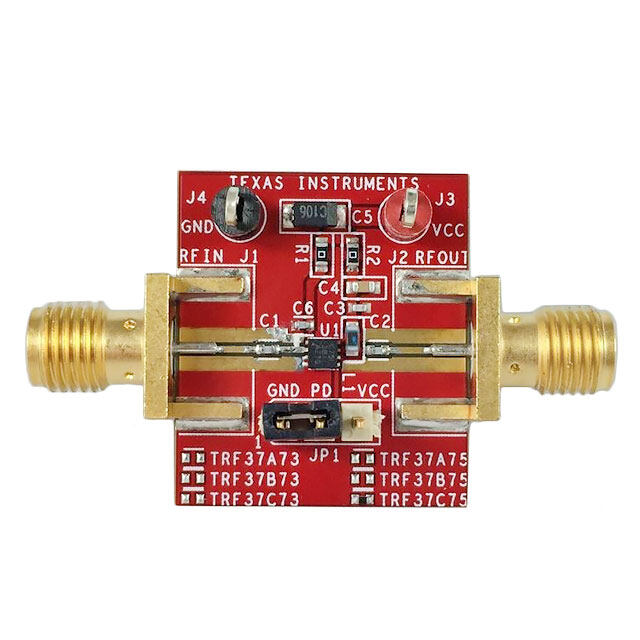
| 产品图片 |
|
| 产品型号 | 124022-HMC799LP3E |
| rohs | 无铅 / 符合限制有害物质指令(RoHS)规范要求 |
| 产品系列 | - |
| 其它名称 | 1127-2162 |
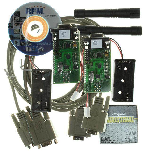
| 所含物品 | 板 |
| 标准包装 | 1 |
| 类型 | |
| 配套使用产品/相关产品 | HMC799LP3E |
| 频率 | 0Hz ~ 700MHz |


- 商务部:美国ITC正式对集成电路等产品启动337调查
- 曝三星4nm工艺存在良率问题 高通将骁龙8 Gen1或转产台积电
- 太阳诱电将投资9.5亿元在常州建新厂生产MLCC 预计2023年完工
- 英特尔发布欧洲新工厂建设计划 深化IDM 2.0 战略
- 台积电先进制程称霸业界 有大客户加持明年业绩稳了
- 达到5530亿美元!SIA预计今年全球半导体销售额将创下新高
- 英特尔拟将自动驾驶子公司Mobileye上市 估值或超500亿美元
- 三星加码芯片和SET,合并消费电子和移动部门,撤换高东真等 CEO
- 三星电子宣布重大人事变动 还合并消费电子和移动部门
- 海关总署:前11个月进口集成电路产品价值2.52万亿元 增长14.8%


PDF Datasheet 数据手册内容提取
HMC799LP3E v01.1009 DC - 700 MHz, 10 kOhm TRANSIMPEDANCE AMPLIFIER Typical Applications Features The HMC799LP3E is ideal for: 10 kOhm Transimpedance • Laser Sensor Very Low Noise: 150nA Input RMS Noise over 700 MHz Bandwidth • FDDI Receiver 700 MHz Analog Bandwidth • CATV FM Analog Receiver Wide Dynamic Range: +65 dB • Wideband Gain Block Low Power: 70mA from Single +5V Supply • Low Noise RF Applications 16 Lead 3x3 mm SMT Package: 9mm² Functional Diagram General Description The HMC799LP3E is DC to 700 MHz Transimpe- dance amplifier designed for opto-electronic laser sensor applications, FDDI receivers and receiver systems employing optical to electrical conversion. This amplifier provides a single-ended output voltage that is proportional to an applied current at its input port. This current is typically provided by a photo- diode. Operating from a single +5V supply, HMC799LP3E features very low input referred noise, and very large electrical input dynamic range exce- 11 eding 65 dB. 10 kOhm or 80 dB-Ohms transimpedance gain provides very good sensitivity at higher data rates. The output of HMC799LP3E is internally matched to T 50 ohms. External matching is not necessary. The M HMC799LP3E exhibits excellent gain and output S power stability over temperature, while requiring a - minimal number of external bias components. S Electrical Specifications, T = +25° C, Vcc1 = Vcc2 = Vcc3 = +5V P A M Parameter Conditions Min. Typ. Max. Units A DC Specifications E Power Supply Voltage 4.5 5 5.5 V C Power Supply Current Vcc = 5V 60 70 80 mA N Input Impedance @ 350 MHz 175 Ohm A Input Bias Voltage 2.1 V D AC Specifications E Transimpedance @ 100 MHz, RL = 50 Ohm 7.5 10 12.5 k Ohms P Transimpedance 3-dB Bandwidth 600 700 MHz M Small Signal Gain S21 42 dB I S Cpd [1] <1pF, @ 200 MHz 4.6 pA / √Hz N Cpd [1] = 1pF, @ 200 MHz 4.8 pA / √Hz Input Referred Current Noise Density A Cpd [1] = 2pF, @ 200 MHz 5.2 pA / √Hz R Cpd [1] = 3pF, @ 200 MHz 5.6 pA / √Hz T [1] Cpd is the total parasitic capacitance value arises from addition of input photo diode. This value includes photo diode parasitic capacitance, PCB trace capacitance and package parasitic capacitance. InfoFrmoarti opn rfiucrneis,h edd eblyi vAenarlyog a Dnedvic etos isp blaelcieeve do trod beer asc:c uHraittet iatned Mreliiacbrleo. wHoawvevee r,C noo rpFoorra tpiroicne,, 2d0el iAvelrpyh, aan Rd otoa dpl,a cCeh oerldmerssf:o Arnda,l oMg AD e0v1ic8e2s4, Inc., responsibility is assumed by Analog Devices for its use, nor for any infringements of patents or other One Technology Way, P.O. Box 9106, Norwood, MA 02062-9106 11 - 1 rliicgehntss eo fi sth girrda nptaerdti ebsy t himatp mlicPaayht ioroens nuolret of:rto hm9er 7wits8is ue-s 2eu.n5 dS0epre- ca3infi3yc ap4tiao3tne sn ts ou rb Fjpeaactte xtno:t cr9higa7hnt8gs e-o 2wf Ai5thn0oaulo-t g3n oD3tiec7vei3.c eN s o. OPrhdoneer: O78n1--3li2n9e- 4a7t0 0w (cid:127)w Owrd.ehri totnitlein.ec aot mwww.analog.com Trademarks and registered trademarks aArep thpe lpircopaetrityo onf thSeiur rpesppeoctrivte: oPwhneorsn.e: 978-250-33A4p3p l icoart i oanp Spusp@pohrti:t Ptihteo.nceo: 1m-800-ANALOG-D
HMC799LP3E v01.1009 DC - 700 MHz, 10 kOhm TRANSIMPEDANCE AMPLIFIER Electrical Specifications (Conditions) Parameter Conditions Min. Typ. Max. Units Cpd [1] <1pF, @ 700 MHz BW 149 nA RMS Cpd [1] = 1pF, @630 MHz BW 164 nA RMS Input Referred RMS Current Noise Cpd [1] = 2pF, @ 560 MHz BW 174 nA RMS Cpd [1] = 3pF, @ 420 MHz BW 132 nA RMS Saturated Output Swing Vin = 50mV p-p 1 Vp-p Output Power 1-dB Compression OP1dB @ 200 MHz 4 dBm Output Third Order Intercept Point OIP3 @ 200 MHz 13 dBm Input Overdrive Current 20 mA Output Return Loss @ 500 MHz 16 20 dB Gain vs. Temperature Output Return Loss vs. Temperature 50 0 +25C 40 -10 +85C B) -40C d GAIN (dB) 2300 ++2855CC URN LOSS (--3200 11 -40C T E R 10 -40 T M 0 -50 S 0 100 200 300 400 500 600 700 800 0 100 200 300 400 500 600 700 800 FREQUENCY (MHz) FREQUENCY (MHz) - S P Input Referred Noise Density vs. M Input Referred Noise Density vs. C [1] Temperature [2] PD A z) z) √A/ H 20 √A/ H 20 E p p C Y ( Cpd=0pF Y ( E DENSIT 15 CCCpppddd===123pppFFF E DENSIT 15 ++ -284550CCC DAN S S NOI 10 NOI 10 E ED ED P R R ER 5 ER 5 M F F E E R R I T T S U U NP 0 NP 0 N I 0 100 200 300 400 500 600 700 800 I 0 100 200 300 400 500 600 700 800 A FREQUENCY (MHz) FREQUENCY (MHz) R [1] Cpd is the total parasitic capacitance value resulting from the addition of the input photo diode. This value includes photo diode parasitic T capacitance, PCB trace capacitance and package parasitic capacitance. [2] Cpd = 1 pF InfoFrmoarti opn rfiucrneis,h edd eblyi vAenarlyog a Dnedvic etos isp blaelcieeve do trod beer asc:c uHraittet iatned Mreliiacbrleo. wHoawvevee r,C noo rpFoorra tpiroicne,, 2d0el iAvelrpyh, aan Rd otoa dpl,a cCeh oerldmerssf:o Arnda,l oMg AD e0v1ic8e2s4, Inc., responsibility is assumed by Analog Devices for its use, nor for any infringements of patents or other One Technology Way, P.O. Box 9106, Norwood, MA 02062-9106 rights of third parties that mPayh roesnulet f:ro m9 7its8 u-s2e.5 S0pe-c3ifi3ca4tio3n s s u bFjeact xto: c9ha7n8ge- 2wi5th0ou-t 3no3tic7e3. N o OPrhdoneer: O78n1--3li2n9e- 4a7t0 0w (cid:127)w Owrd.ehri totnitlein.ec aot mwww.analog.com 11 - 2 license is granted by implication or otherwise under any patent or patent rights of Analog Devices. Trademarks and registered trademarks aArep thpe lpircopaetrityo onf thSeiur rpesppeoctrivte: oPwhneorsn.e: 978-250-33A4p3p l icoart i oanp Spusp@pohrti:t Ptihteo.nceo: 1m-800-ANALOG-D
HMC799LP3E v01.1009 DC - 700 MHz, 10 kOhm TRANSIMPEDANCE AMPLIFIER Transimpedance vs. Transimpedance vs. C [1] Supply Voltage (Vcc) [2] PD 20 20 C =0pF Ohm) 15 CCppdd==12ppFF Ohm) 15 VVcccc==45..50VV E (k Cppdd=3pF E (k Vcc=5.5V C C N N DA 10 DA 10 E E P P M M SI SI N N A 5 A 5 R R T T 0 0 0 100 200 300 400 500 600 700 800 0 100 200 300 400 500 600 700 800 FREQUENCY (MHz) FREQUENCY (MHz) Output Power vs. Transimpedance vs. Temperature [2] Input Power @ 200 MHz [2] 20 10 m) 11 DANCE (kOh 1105 OWER (dBm) 05 E P MP UT SI P T TRAN 5 ++ -284550CCC OUT -5 M S 00 100 200 300 400 500 600 700 800 -10-50 -40 -30 -20 -10 0 10 - FREQUENCY (MHz) INPUT POWER (dBm) S P [1] Cpd is the total parasitic capacitance value resulting from the addition of the input photo diode. This value includes photo diode parasitic M capacitance, PCB trace capacitance and package parasitic capacitance. [2] Cpd = 1 pF A E C N A D E P M I S N A R T InfoFrmoarti opn rfiucrneis,h edd eblyi vAenarlyog a Dnedvic etos isp blaelcieeve do trod beer asc:c uHraittet iatned Mreliiacbrleo. wHoawvevee r,C noo rpFoorra tpiroicne,, 2d0el iAvelrpyh, aan Rd otoa dpl,a cCeh oerldmerssf:o Arnda,l oMg AD e0v1ic8e2s4, Inc., responsibility is assumed by Analog Devices for its use, nor for any infringements of patents or other One Technology Way, P.O. Box 9106, Norwood, MA 02062-9106 11 - 3 rliicgehntss eo fi sth girrda nptaerdti ebsy t himatp mlicPaayht ioroens nuolret of:rto hm9er 7wits8is ue-s 2eu.n5 dS0epre- ca3infi3yc ap4tiao3tne sn ts ou rb Fjpeaactte xtno:t cr9higa7hnt8gs e-o 2wf Ai5thn0oaulo-t g3n oD3tiec7vei3.c eN s o. OPrhdoneer: O78n1--3li2n9e- 4a7t0 0w (cid:127)w Owrd.ehri totnitlein.ec aot mwww.analog.com Trademarks and registered trademarks aArep thpe lpircopaetrityo onf thSeiur rpesppeoctrivte: oPwhneorsn.e: 978-250-33A4p3p l icoart i oanp Spusp@pohrti:t Ptihteo.nceo: 1m-800-ANALOG-D
HMC799LP3E v01.1009 DC - 700 MHz, 10 kOhm TRANSIMPEDANCE AMPLIFIER Output Signal [1] Measurements Current Mean std dev Min. Max Units V amptd 198.84 200.50 3.6253 184.99 212.70 mV Frequency 200.8 199.9 0.631 198.0 202.1 MHz Duty Cycle 50.9 49.7 0.62 47.6 51.6 % [1] Input signal current 25 µAp-p, frequency 200 MHz Output Signal [2] Measurements Current Mean std dev Min. Max Units V amptd 959.62 960.47 3.703 953.11 972.63 mV Frequency 200.1 200.0 0.117 199.5 200.4 MHz 11 Duty Cycle 49.1 49 0.08 48.7 49.2 % [2] Input signal current 20 mAp-p, frequency 200 MHz T M S - S P M A E C N A D E P M I S N A R T InfoFrmoarti opn rfiucrneis,h edd eblyi vAenarlyog a Dnedvic etos isp blaelcieeve do trod beer asc:c uHraittet iatned Mreliiacbrleo. wHoawvevee r,C noo rpFoorra tpiroicne,, 2d0el iAvelrpyh, aan Rd otoa dpl,a cCeh oerldmerssf:o Arnda,l oMg AD e0v1ic8e2s4, Inc., responsibility is assumed by Analog Devices for its use, nor for any infringements of patents or other One Technology Way, P.O. Box 9106, Norwood, MA 02062-9106 rights of third parties that mPayh roesnulet f:ro m9 7its8 u-s2e.5 S0pe-c3ifi3ca4tio3n s s u bFjeact xto: c9ha7n8ge- 2wi5th0ou-t 3no3tic7e3. N o OPrhdoneer: O78n1--3li2n9e- 4a7t0 0w (cid:127)w Owrd.ehri totnitlein.ec aot mwww.analog.com 11 - 4 license is granted by implication or otherwise under any patent or patent rights of Analog Devices. Trademarks and registered trademarks aArep thpe lpircopaetrityo onf thSeiur rpesppeoctrivte: oPwhneorsn.e: 978-250-33A4p3p l icoart i oanp Spusp@pohrti:t Ptihteo.nceo: 1m-800-ANALOG-D
HMC799LP3E v01.1009 DC - 700 MHz, 10 kOhm TRANSIMPEDANCE AMPLIFIER Absolute Maximum Ratings Power Supply Voltage -1V to 8V (Vcc1, Vcc2, Vcc3) Input Current 30 mAp-p Junction Temperature 125 °C Continuous Pdiss (T=85 °C) 1.27W (derate 31.82 mW/ °C Above +85 °C Thermal Resistance 31.43 °C/W (Junction to ground paddle) Storage Temperature -65 to 125 °C Operating Temperature -40 to +85 °C ESD Sensitivity (HBM) Class 1C Outline Drawing 11 T M S - S P M A E NOTES: 1. LEADFRAME MATERIAL: COPPER ALLOY C 2. DIMENSIONS ARE IN INCHES [MILLIMETERS]. N 3. LEAD SPACING TOLERANCE IS NON-CUMULATIVE A 4. PAD BURR LENGTH SHALL BE 0.15mm MAXIMUM. D PAD BURR HEIGHT SHALL BE 0.05mm MAXIMUM. 5. PACKAGE WARP SHALL NOT EXCEED 0.05mm. E 6. ALL GROUND LEADS AND GROUND PADDLE P MUST BE SOLDERED TO PCB RF GROUND. M 7. REFER TO HMC APPLICATION NOTE FOR SUGGESTED PCB LAND PATTERN. I Package Information S N Part Number Package Body Material Lead Finish MSL Rating Package Marking [1] A HMC799LP3E RoHS-compliant Low Stress Injection Molded Plastic 100% matte Sn MSL1 [2] H799 R XXXX T [1] 4-Digit lot number XXXX [2] Max peak reflow temperature of 260 °C InfoFrmoarti opn rfiucrneis,h edd eblyi vAenarlyog a Dnedvic etos isp blaelcieeve do trod beer asc:c uHraittet iatned Mreliiacbrleo. wHoawvevee r,C noo rpFoorra tpiroicne,, 2d0el iAvelrpyh, aan Rd otoa dpl,a cCeh oerldmerssf:o Arnda,l oMg AD e0v1ic8e2s4, Inc., responsibility is assumed by Analog Devices for its use, nor for any infringements of patents or other One Technology Way, P.O. Box 9106, Norwood, MA 02062-9106 11 - 5 rliicgehntss eo fi sth girrda nptaerdti ebsy t himatp mlicPaayht ioroens nuolret of:rto hm9er 7wits8is ue-s 2eu.n5 dS0epre- ca3infi3yc ap4tiao3tne sn ts ou rb Fjpeaactte xtno:t cr9higa7hnt8gs e-o 2wf Ai5thn0oaulo-t g3n oD3tiec7vei3.c eN s o. OPrhdoneer: O78n1--3li2n9e- 4a7t0 0w (cid:127)w Owrd.ehri totnitlein.ec aot mwww.analog.com Trademarks and registered trademarks aArep thpe lpircopaetrityo onf thSeiur rpesppeoctrivte: oPwhneorsn.e: 978-250-33A4p3p l icoart i oanp Spusp@pohrti:t Ptihteo.nceo: 1m-800-ANALOG-D
HMC799LP3E v01.1009 DC - 700 MHz, 10 kOhm TRANSIMPEDANCE AMPLIFIER Pin Descriptions Pin Number Function Description Interface Schematic VCC1, VCC2, 1, 12, 14 Positive Supply VCC3 2 CFILT Overload current filter capacitance pin. 3 RFIN RF Input 4 CEXT Reference voltage filter capacitance pin. 11 5 - 9, 11, N/C Not connected. 13, 15, 16 T M S 10 RFOUT RF Output - S P M Package Package base has exposed metal ground GND Base paddle which must be connected to ground. A E C N A D E P M I S N A R T InfoFrmoarti opn rfiucrneis,h edd eblyi vAenarlyog a Dnedvic etos isp blaelcieeve do trod beer asc:c uHraittet iatned Mreliiacbrleo. wHoawvevee r,C noo rpFoorra tpiroicne,, 2d0el iAvelrpyh, aan Rd otoa dpl,a cCeh oerldmerssf:o Arnda,l oMg AD e0v1ic8e2s4, Inc., responsibility is assumed by Analog Devices for its use, nor for any infringements of patents or other One Technology Way, P.O. Box 9106, Norwood, MA 02062-9106 rights of third parties that mPayh roesnulet f:ro m9 7its8 u-s2e.5 S0pe-c3ifi3ca4tio3n s s u bFjeact xto: c9ha7n8ge- 2wi5th0ou-t 3no3tic7e3. N o OPrhdoneer: O78n1--3li2n9e- 4a7t0 0w (cid:127)w Owrd.ehri totnitlein.ec aot mwww.analog.com 11 - 6 license is granted by implication or otherwise under any patent or patent rights of Analog Devices. Trademarks and registered trademarks aArep thpe lpircopaetrityo onf thSeiur rpesppeoctrivte: oPwhneorsn.e: 978-250-33A4p3p l icoart i oanp Spusp@pohrti:t Ptihteo.nceo: 1m-800-ANALOG-D
HMC799LP3E v01.1009 DC - 700 MHz, 10 kOhm TRANSIMPEDANCE AMPLIFIER Application Circuit 11 T Note: M For power supply rejection ratio (PSRR) tests, install 0 Ohm for R1. S - S P M A E C N A D E P M I S N A R T InfoFrmoarti opn rfiucrneis,h edd eblyi vAenarlyog a Dnedvic etos isp blaelcieeve do trod beer asc:c uHraittet iatned Mreliiacbrleo. wHoawvevee r,C noo rpFoorra tpiroicne,, 2d0el iAvelrpyh, aan Rd otoa dpl,a cCeh oerldmerssf:o Arnda,l oMg AD e0v1ic8e2s4, Inc., responsibility is assumed by Analog Devices for its use, nor for any infringements of patents or other One Technology Way, P.O. Box 9106, Norwood, MA 02062-9106 11 - 7 rliicgehntss eo fi sth girrda nptaerdti ebsy t himatp mlicPaayht ioroens nuolret of:rto hm9er 7wits8is ue-s 2eu.n5 dS0epre- ca3infi3yc ap4tiao3tne sn ts ou rb Fjpeaactte xtno:t cr9higa7hnt8gs e-o 2wf Ai5thn0oaulo-t g3n oD3tiec7vei3.c eN s o. OPrhdoneer: O78n1--3li2n9e- 4a7t0 0w (cid:127)w Owrd.ehri totnitlein.ec aot mwww.analog.com Trademarks and registered trademarks aArep thpe lpircopaetrityo onf thSeiur rpesppeoctrivte: oPwhneorsn.e: 978-250-33A4p3p l icoart i oanp Spusp@pohrti:t Ptihteo.nceo: 1m-800-ANALOG-D
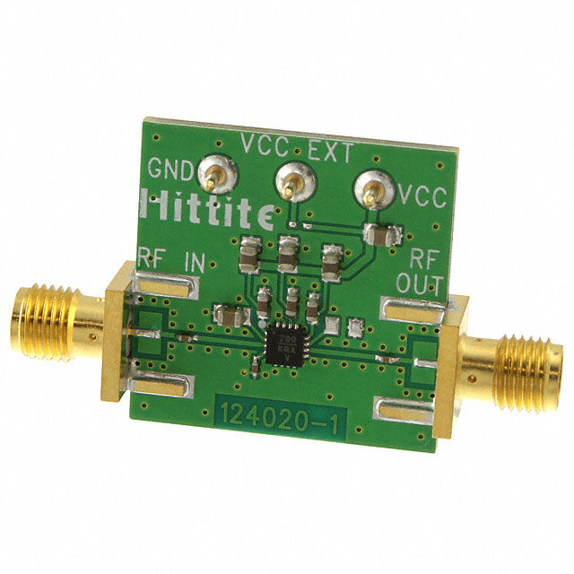
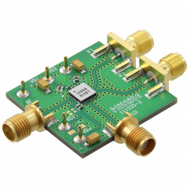
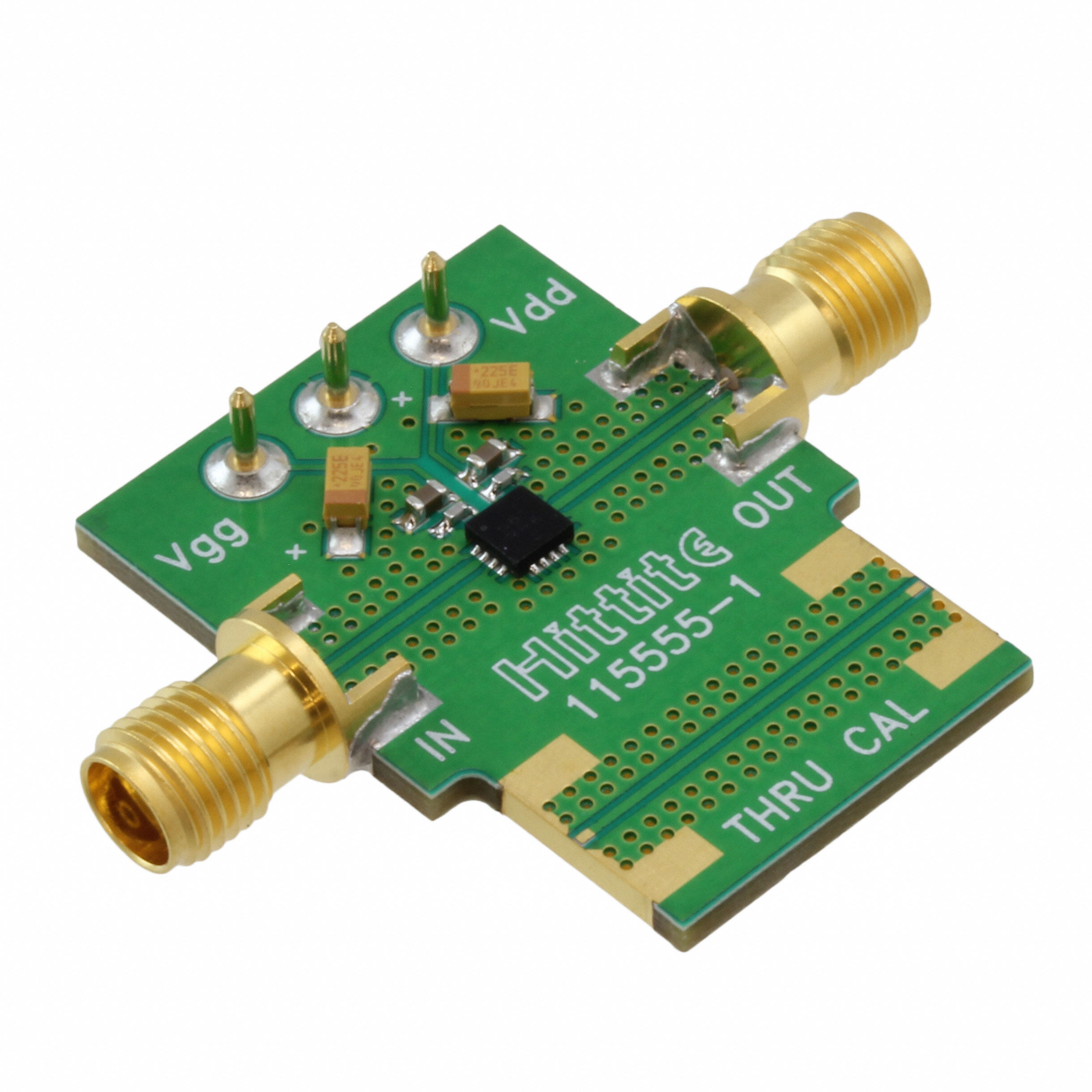
HMC799LP3E v01.1009 DC - 700 MHz, 10 kOhm TRANSIMPEDANCE AMPLIFIER Evaluation PCB 11 T M S - S P M List of Materials for Evaluation PCB 124022 [1] A The circuit board used in the final application Item Description should use RF circuit design techniques. Signal E J1 - J2 PCB Mount SMA Connector C lines should have 50 ohm impedance while the J3, J5 DC Pin N package ground leads and exposed paddle should C1 - C3 22 nF Capacitor, 0402 Pkg. A be connected directly to the ground plane similar C4, C12 10 µF Capacitor, 0805 Pkg. D to that shown. A sufficient number of via holes C6, C8, C10 4.7 µF Capacitor, 0805 Pkg. E should be used to connect the top and bottom C7, C9, C11 0.1 µF Capacitor, 0603 Pkg. P ground planes. The evaluation circuit board shown U1 HMC799LP3E Transimpedance Amplifier M is available from Hittite upon request. PCB [2] 124020 Evaluation PCB I S [1] Reference this number when ordering complete evaluation PCB N [2] Circuit Board Material: Arlon 25FR or Rogers 4350 A R T InfoFrmoarti opn rfiucrneis,h edd eblyi vAenarlyog a Dnedvic etos isp blaelcieeve do trod beer asc:c uHraittet iatned Mreliiacbrleo. wHoawvevee r,C noo rpFoorra tpiroicne,, 2d0el iAvelrpyh, aan Rd otoa dpl,a cCeh oerldmerssf:o Arnda,l oMg AD e0v1ic8e2s4, Inc., responsibility is assumed by Analog Devices for its use, nor for any infringements of patents or other One Technology Way, P.O. Box 9106, Norwood, MA 02062-9106 rights of third parties that mPayh roesnulet f:ro m9 7its8 u-s2e.5 S0pe-c3ifi3ca4tio3n s s u bFjeact xto: c9ha7n8ge- 2wi5th0ou-t 3no3tic7e3. N o OPrhdoneer: O78n1--3li2n9e- 4a7t0 0w (cid:127)w Owrd.ehri totnitlein.ec aot mwww.analog.com 11 - 8 license is granted by implication or otherwise under any patent or patent rights of Analog Devices. Trademarks and registered trademarks aArep thpe lpircopaetrityo onf thSeiur rpesppeoctrivte: oPwhneorsn.e: 978-250-33A4p3p l icoart i oanp Spusp@pohrti:t Ptihteo.nceo: 1m-800-ANALOG-D