ICGOO在线商城 > 射频/IF 和 RFID > RF 评估和开发套件,板 > 103802-HMC308
 Datasheet下载
- 型号: 103802-HMC308
- 制造商: Hittite
- 库位|库存: xxxx|xxxx
- 要求:
| 数量阶梯 | 香港交货 | 国内含税 |
| +xxxx | $xxxx | ¥xxxx |
查看当月历史价格
查看今年历史价格
103802-HMC308产品简介:
ICGOO电子元器件商城为您提供103802-HMC308由Hittite设计生产,在icgoo商城现货销售,并且可以通过原厂、代理商等渠道进行代购。 103802-HMC308价格参考。Hittite103802-HMC308封装/规格:RF 评估和开发套件,板, 。您可以下载103802-HMC308参考资料、Datasheet数据手册功能说明书,资料中有103802-HMC308 详细功能的应用电路图电压和使用方法及教程。
型号为103802-HMC308的RF评估和开发套件由Analog Devices Inc.提供,主要用于射频(RF)应用的设计、测试与验证。以下是其主要应用场景:

 1. 射频信号放大
   - HMC308是一款宽带射频放大器,适用于需要高增益、低噪声和宽带宽的场景。该开发套件可帮助工程师评估其在不同频率范围内的性能。
   - 应用领域:无线通信基站、卫星通信、雷达系统等。

 2. 无线通信系统
   - 该套件可用于测试和优化无线通信系统的前端设计,例如蜂窝网络(如4G LTE、5G NR)、Wi-Fi和其他无线标准中的信号放大和处理。
   - 特别适合需要高线性度和大动态范围的应用。

 3. 测试与测量设备
   - 在测试与测量领域,HMC308可用作信号增强模块,以提高测试仪器的灵敏度和精度。
   - 应用场景包括频谱分析仪、网络分析仪和信号发生器等。

 4. 航空航天与国防
   - 由于其高频性能和可靠性,HMC308广泛应用于航空航天和国防领域,例如雷达系统、电子对抗(ECM)和卫星通信。
   - 开发套件允许用户评估其在极端环境下的表现。

 5. 点对点微波链路
   - 在点对点微波通信中,HMC308可用于信号放大,以确保长距离传输时的信号完整性。
   - 套件支持用户调整增益和匹配阻抗,以适应特定的链路预算需求。

 6. 医疗设备
   - 某些医疗成像设备(如超声波或MRI)需要高性能的射频组件来处理高频信号。HMC308的低噪声特性和宽带能力使其成为这些应用的理想选择。

 7. 物联网(IoT)和工业自动化
   - 在IoT和工业自动化中,该套件可用于评估射频模块的性能,特别是在需要远程通信或高数据速率的场景下。

通过使用103802-HMC308开发套件,工程师可以快速评估HMC308放大器的性能参数(如增益、噪声系数、输入/输出功率等),并将其集成到各种射频系统中,从而加速产品开发周期。
| 参数 | 数值 |
| 产品目录 | |
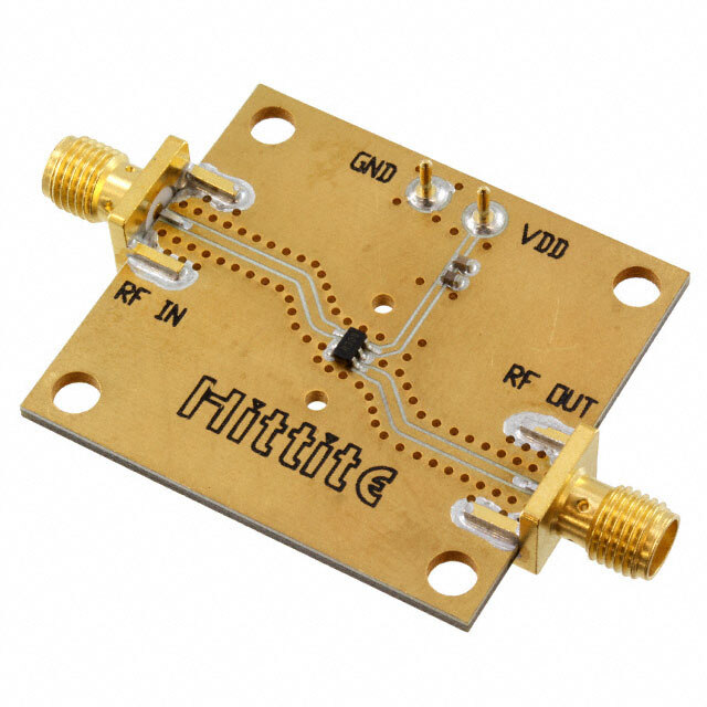
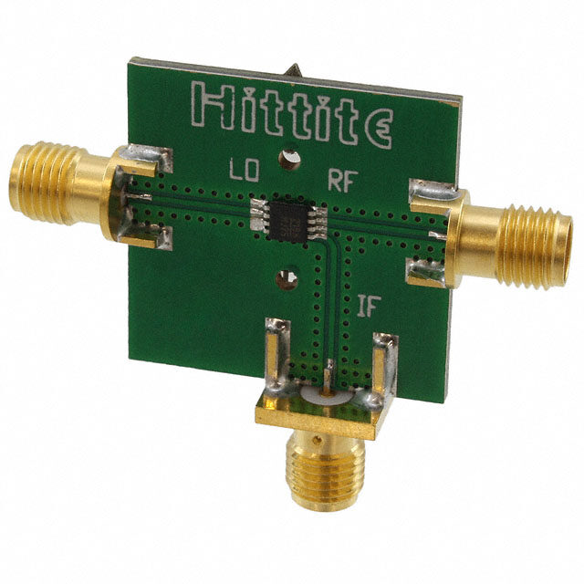
| 描述 | BOARD EVAL AMPLIFIER MMIC HMC308 |
| 产品分类 | |
| 品牌 | Hittite Microwave Corporation |
| 数据手册 | |
| 产品图片 |
|
| 产品型号 | 103802-HMC308 |
| rohs | 无铅 / 符合限制有害物质指令(RoHS)规范要求 |
| 产品系列 | - |
| 其它名称 | 103802HMC308 |
| 所含物品 | 板 |
| 标准包装 | 1 |
| 类型 | 放大器,MMIC |
| 配套使用产品/相关产品 | HMC308 |
| 频率 | 800kHz ~ 3.8GHz |


- 商务部:美国ITC正式对集成电路等产品启动337调查
- 曝三星4nm工艺存在良率问题 高通将骁龙8 Gen1或转产台积电
- 太阳诱电将投资9.5亿元在常州建新厂生产MLCC 预计2023年完工
- 英特尔发布欧洲新工厂建设计划 深化IDM 2.0 战略
- 台积电先进制程称霸业界 有大客户加持明年业绩稳了
- 达到5530亿美元!SIA预计今年全球半导体销售额将创下新高
- 英特尔拟将自动驾驶子公司Mobileye上市 估值或超500亿美元
- 三星加码芯片和SET,合并消费电子和移动部门,撤换高东真等 CEO
- 三星电子宣布重大人事变动 还合并消费电子和移动部门
- 海关总署:前11个月进口集成电路产品价值2.52万亿元 增长14.8%


PDF Datasheet 数据手册内容提取
HMC308 308E / v05.1107 GENERAL PURPOSE 100 mW GaAs MMIC AMPLIFIER, 0.8 - 3.8 GHz Typical Applications Features 9 Broadband or Narrow Band Applications: Gain: 18 dB • Cellular/PCS/3G P1dB Output Power: +17 dBm@ +5V • Fixed Wireless & Telematics Single Supply: +3V or +5V T E • Cable Modem Termination Systems No External Components M S • WLAN, Bluetooth & RFID Integrated DC Blocks - Ultra Small Package: SOTT26 S R E Functional Diagram General DeEscription I F I The HMC308 & HMC308E are low cost MESFET L P MMIC amplifi ers that operate from a single +3 to L M +5V supply from 0.8 to 3.8 GHz. The surface mount A SOT26 amplifi er can be used as a broadband ampli- fi er stage or used with external matching for opti- K O mized narrow band applications. With Vdd biased at C +5V, the HMC308 & HMC308E offers 18 dB of gain O and +20 dBm of saturated output power while requir- L B ing only 53 mA of current. This amplifi er is ideal as S a driver amplifi er for transmitters or for use as a N local oscillator (LO) amplifi er to increase drive levels I A for passive mixers. The amplifi er occupies 0.014 in2 G B (9 mm2), making it ideal for compact radio designs. & R E O V RI Electrical Specifi cations, T = +25° C, as a function of Vdd A D Vdd = +3V Vdd = +5V Vdd = +5V Vdd = +5V Parameter Units Min. Typ. Max. Min. Typ. Max. Min. Typ. Max. Min. Typ. Max. Frequency Range 2.3 - 2.7 0.8 - 2.3 2.3 - 2.7 2.7 - 3.8 GHz Gain 13 15.5 14 18 13 16 10 13 dB Gain Variation over Temperature 0.025 0.035 0.025 0.035 0.025 0.035 0.025 0.035 dB/°C Input Return Loss 11 8 11 13 dB Output Return Loss 17 13 12 13 dB Output Power for 1 dB 12 14 14 17 13.5 16.5 12 15 dBm Compression (P1dB) Saturated Output Power (Psat) 17 20 19.5 17 dBm Output Third Order Intercept (IP3) 23 26 27 30 26 29 24 27 dBm Noise Figure 7 7.5 7 7 dB Supply Current (Idd) 50 53 53 53 mA Information furnisheFd obry Apnrailcoge D, edviceelsi vise breylie,v eadn tdo bteo a cpcluaractee a nod rrdelieabrlse., Hpowleevaers, eno coFnotra pcritc eH, idtteiltieve rMy, iacnrdo wtoa pvlaec eC oorrdperosr: aAtnioalnog: Devices, Inc., responsibility is assumed by Analog Devices for its use, nor for any infringements of patents or other One Technology Way, P.O. Box 9106, Norwood, MA 02062-9106 9 - 2 rights of third parties th2at 0m aAy rlepsuhlt afro mR iots ausde., S Cpehcifeicalmtionss fsoubrjdec,t tMo cAhan 0ge1 w8it2ho4ut n oPticheo. Nnoe : P9h7o8ne-:2 75801--33239-44370 0F (cid:127)a Oxr:d 9er7 o8n-li2ne5 a0t- w3w3w7.3analog.com license is granted by implication or otherwise under any patent or patent rights of Analog Devices. Trademarks and registered trademarks are the property of their resOpercdtivee orw Onerns.-line at www.hAiptptilticea.tcioonm Support: Phone: 1-800-ANALOG-D
HMC308 / 308E v05.1107 GENERAL PURPOSE 100 mW GaAs MMIC AMPLIFIER, 0.8 - 3.8 GHz Broadband Gain & Return Loss @ Vdd = +5V P1dB vs. Vdd Bias 9 30 24 20 20 B) 10 16 RESPONSE (d -100 SSS122112 P1dB (dBm) 182 VVdddd==++53VVE SMT T - -20 4 S R -30 0 E 0.5 1 1.5 2 2.5 3 3.5 4 4.5 5 0.5 1 E1.5 2 2.5 3 3.5 4 I FREQUENCY (GHz) FREQUENCY (GHz) F I L P L M Gain vs. Temperature @ Vdd = +5V Gain vs. Temperature @ Vdd = +3V A 24 24 K O 20 20 C O 16 16 B) B) L d d GAIN ( 12 +25 C S GAIN ( 12 +25 C N B 8 +85 C 8 +85 C -40 C -40 C I A 4 4 B G 0 0 & 0.5 1 1.5 2 2.5 3 3.5 4 0.5 1 1.5 2 2.5 3 3.5 4 FREQUENCY (GHz) FREQUENCY (GHz) R O E V Input & Output I Return Loss vs. Vdd Bias Reverse Isolation vs. Vdd Bias R D 0 0 -5 B) -10 d S (dB) -10 TION ( -20 VVdddd==++53VV S -15 A O L L O -30 RN -20 E IS U S T R -40 RE -25 S11 Vdd=+5V EVE -30 SS2121 VVdddd==++53VV R -50 S22 Vdd=+3V -35 -60 0.5 1 1.5 2 2.5 3 3.5 4 0.5 1 1.5 2 2.5 3 3.5 4 FREQUENCY (GHz) FREQUENCY (GHz) Information furnisheFd obry Apnrailcoge D, edviceelsi vise breylie,v eadn tdo bteo a cpcluaractee a nod rrdelieabrlse., Hpowleevaers, eno coFnotra pcritc eH, idtteiltieve rMy, iacnrdo wtoa pvlaec eC oorrdperosr: aAtnioalnog: Devices, Inc., responsibility is assumed by Analog Devices for its use, nor for any infringements of patents or other One Technology Way, P.O. Box 9106, Norwood, MA 02062-9106 rights of third parties tha2t 0ma yA relpsuhlt faro mR itos uasde. ,S pCechifiecaltmionss fsoubrjedct, toM chAan g0e1 w8ith2ou4t nPotihceo. Nnoe : P9h7o8n-e2: 75801--332394-437 0 0F (cid:127)a Ox:r d9e7r o8n-l2in5e 0at- w33w7w3.analog.com 9 - 3 license is granted by implication or otherwise under any patent or patent rights of Analog Devices. Trademarks and registered trademarks are the property of their resOpercdtivee orw Onerns.-line at www.hAiptptilticea.tcioonm Support: Phone: 1-800-ANALOG-D
HMC308 / 308E v05.1107 GENERAL PURPOSE 100 mW GaAs MMIC AMPLIFIER, 0.8 - 3.8 GHz Power Compression Power Compression @ 2.0 GHz, Vdd = +5V @ 2.5 GHz, Vdd = +5V 9 28 28 %) 24 GPoauint %) 24 Pout AE ( 20 PAE AE ( 20 GPAaiEn P P T B), 16 B), 16 E d d M AIN ( 12 AIN ( 12 S m), G 8 m), G 8 B B S - out (d 4 out (d 4 T P 0 P 0 R -4 -4 E -20 -18 -16 -14 -12 -10 -8 -6 -4 -2 0 2 4 6 -20 -18 -16 E-14 -12 -10 -8 -6 -4 -2 0 2 4 6 I F INPUT POWER (dBm) INPUT POWER (dBm) I L P OutLput P1dB vs. M Psat vs. Temperature @ Vdd = +5V Temperature @ Vdd = +5V A 24 24 K O C 20 20 O L m) 16 m) 16 N B Psat (dB 12 ++2855 CC S P1dB (dB 12 ++2855 CC -40 C -40 C I A 8 8 G B 4 4 & 0.5 1 1.5 2 2.5 3 3.5 4 0.5 1 1.5 2 2.5 3 3.5 4 R FREQUENCY (GHz) FREQUENCY (GHz) E O V Output IP3 I R vs. Temperature @ Vdd = +5V Typical Supply Current vs. Vdd D 38 Vdd (Vdc) Idd (mA) 34 +2.5 49 30 +3.0 50 26 +3.5 51 m) B d 22 +4.5 50 P3 ( ++2855 CC I 18 -40 C +5.0 53 14 +5.5 54 10 6 0.5 1 1.5 2 2.5 3 3.5 4 FREQUENCY (GHz) Information furnisheFd obry Apnrailcoge D, edviceelsi vise breylie,v eadn tdo bteo a cpcluaractee a nod rrdelieabrlse., Hpowleevaers, eno coFnotra pcritc eH, idtteiltieve rMy, iacnrdo wtoa pvlaec eC oorrdperosr: aAtnioalnog: Devices, Inc., responsibility is assumed by Analog Devices for its use, nor for any infringements of patents or other One Technology Way, P.O. Box 9106, Norwood, MA 02062-9106 9 - 4 rights of third parties th2at 0m aAy rlepsuhlt afro mR iots ausde., S Cpehcifeicalmtionss fsoubrjdec,t tMo cAhan 0ge1 w8it2ho4ut n oPticheo. Nnoe : P9h7o8ne-:2 75801--33239-44370 0F (cid:127)a Oxr:d 9er7 o8n-li2ne5 a0t- w3w3w7.3analog.com license is granted by implication or otherwise under any patent or patent rights of Analog Devices. Trademarks and registered trademarks are the property of their resOpercdtivee orw Onerns.-line at www.hAiptptilticea.tcioonm Support: Phone: 1-800-ANALOG-D
HMC308 / 308E v05.1107 GENERAL PURPOSE 100 mW GaAs MMIC AMPLIFIER, 0.8 - 3.8 GHz Power Compression Power Compression @ 2.0 GHz, Vdd = +3V @ 2.5 GHz, Vdd = +3V 9 30 28 28 AE (%) 222246 GPPoAauiEnt AE (%) 2204 GPPoAauiEnt P 20 P B), 18 B), 16 E T d 16 d AIN ( 1124 AIN ( 12 M m), G 180 m), G 8 S Pout (dB 0246 Pout (dB 04 T S - R -2 -4 -4 E -20 -18 -16 -14 -12 -10 -8 -6 -4 -2 0 2 4 6 -20 -18 -16 E-14 -12 -10 -8 -6 -4 -2 0 2 4 6 I INPUT POWER (dBm) INPUT POWER (dBm) F I L Output P1dB vs. P L M Psat vs. Temperature @ Vdd = +3V Temperature @ Vdd = +3V A 24 24 K O 20 20 C O Psat (dBm) 1126 ++2855 CC S P1dB (dBm) 1126 N BL -40 C I 8 8 ++2855 CC A B -40 C G 4 4 & 0.5 1 1.5 2 2.5 3 3.5 4 0.5 1 1.5 2 2.5 3 3.5 4 FREQUENCY (GHz) FREQUENCY (GHz) R O E V Output IP3 I vs. Temperature @ Vdd = +3V Absolute Maximum Ratings R D 38 Drain Bias Voltage (Vdd) +7.0 Vdc 34 RF Input Power (RFIN)(Vdd = +5Vdc) +10 dBm 30 Channel Temperature 150 °C m) 26 C(doenratitneu 6o.u2s5 P mdWiss/° C(T a=b 8ov5e ° C85) °C) 0.406 W B d 22 IP3 ( 18 +25 C T(chhearnmnaell Rtoe lseisatda)nce 160 °C/W +85 C 14 -40 C Storage Temperature -65 to +150 °C Operating Temperature -40 to +85 °C 10 ESD Sensitivity (HBM) Class 1A 6 0.5 1 1.5 2 2.5 3 3.5 4 FREQUENCY (GHz) ELECTROSTATIC SENSITIVE DEVICE OBSERVE HANDLING PRECAUTIONS Information furnisheFd obry Apnrailcoge D, edviceelsi vise breylie,v eadn tdo bteo a cpcluaractee a nod rrdelieabrlse., Hpowleevaers, eno coFnotra pcritc eH, idtteiltieve rMy, iacnrdo wtoa pvlaec eC oorrdperosr: aAtnioalnog: Devices, Inc., responsibility is assumed by Analog Devices for its use, nor for any infringements of patents or other One Technology Way, P.O. Box 9106, Norwood, MA 02062-9106 rights of third parties tha2t 0ma yA relpsuhlt faro mR itos uasde. ,S pCechifiecaltmionss fsoubrjedct, toM chAan g0e1 w8ith2ou4t nPotihceo. Nnoe : P9h7o8n-e2: 75801--332394-437 0 0F (cid:127)a Ox:r d9e7r o8n-l2in5e 0at- w33w7w3.analog.com 9 - 5 license is granted by implication or otherwise under any patent or patent rights of Analog Devices. Trademarks and registered trademarks are the property of their resOpercdtivee orw Onerns.-line at www.hAiptptilticea.tcioonm Support: Phone: 1-800-ANALOG-D
HMC308 / 308E v05.1107 GENERAL PURPOSE 100 mW GaAs MMIC AMPLIFIER, 0.8 - 3.8 GHz Outline Drawing 9 T E M S - T S R E E I F I L P NOTES: 1. LEALDFRAME MATERIAL: COPPER ALLOY M 2. DIMENSIONS ARE IN INCHES [MILLIMETERS] A 3. DIMENSION DOES NOT INCLUDE MOLDFLASH OF 0.15mm PER SIDE. 4. DIMENSION DOES NOT INCLUDE MOLDFLASH OF 0.25mm PER SIDE. K O 5. ALL GROUND LEADS MUST BE SOLDERED TO PCB RF GROUND C O L B S N I A Package Information G Part Number PacBkage Body Material Lead Finish MSL Rating Package Marking [3] & HMC308 Low Stress Injection Molded Plastic Sn/Pb Solder MSL1 [1] H308 XXXX R HMC308E RoHS-compliant Low Stress Injection Molded Plastic 100% matte Sn MSL1 [2] 308E E O XXXX V [1] Max peak refl ow temperature of 235 °C I [2] Max peak refl ow temperature of 260 °C R [3] 4-Digit lot number XXXX D Pin Descriptions Pin Number Function Description Interface Schematic 1 RFOUT This pin is AC coupled and matched to 50 Ohms. 2, 5, 6 GND These pins must be connected to RF/DC ground. 3 Vdd Power supply voltage. 4 RFIN This pin is AC coupled and matched to 50 Ohms. Information furnisheFd obry Apnrailcoge D, edviceelsi vise breylie,v eadn tdo bteo a cpcluaractee a nod rrdelieabrlse., Hpowleevaers, eno coFnotra pcritc eH, idtteiltieve rMy, iacnrdo wtoa pvlaec eC oorrdperosr: aAtnioalnog: Devices, Inc., responsibility is assumed by Analog Devices for its use, nor for any infringements of patents or other One Technology Way, P.O. Box 9106, Norwood, MA 02062-9106 9 - 6 rights of third parties th2at 0m aAy rlepsuhlt afro mR iots ausde., S Cpehcifeicalmtionss fsoubrjdec,t tMo cAhan 0ge1 w8it2ho4ut n oPticheo. Nnoe : P9h7o8ne-:2 75801--33239-44370 0F (cid:127)a Oxr:d 9er7 o8n-li2ne5 a0t- w3w3w7.3analog.com license is granted by implication or otherwise under any patent or patent rights of Analog Devices. Trademarks and registered trademarks are the property of their resOpercdtivee orw Onerns.-line at www.hAiptptilticea.tcioonm Support: Phone: 1-800-ANALOG-D
HMC308 / 308E v05.1107 GENERAL PURPOSE 100 mW GaAs MMIC AMPLIFIER, 0.8 - 3.8 GHz Evaluation PCB 9 E T M S T - S R E E I F I L P L M A K O C O L B S N I A B G & R O E V I List of Materials for Evaluation PCB 103802 [1] R D The circuit board used in the fi nal application should Item Description use RF circuit design techniques. Signal lines should J1, J2 PCB Mount SMA Connector have 50 ohm impedance while the package ground J3, J4 DC Pins leads should be connected directly to the ground U1 HMC308 / HMC308E Amplifi er plane similar to that shown. A sufficient number of PCB [2] 103220 Evaluation Board via holes should be used to connect the top and [1] Reference this number when ordering complete evaluation PCB bottom ground planes. The evaluation circuit board [2] Circuit Board Material: Roger 4350 shown is available from Hittite upon request. Information furnisheFd obry Apnrailcoge D, edviceelsi vise breylie,v eadn tdo bteo a cpcluaractee a nod rrdelieabrlse., Hpowleevaers, eno coFnotra pcritc eH, idtteiltieve rMy, iacnrdo wtoa pvlaec eC oorrdperosr: aAtnioalnog: Devices, Inc., responsibility is assumed by Analog Devices for its use, nor for any infringements of patents or other One Technology Way, P.O. Box 9106, Norwood, MA 02062-9106 rights of third parties tha2t 0ma yA relpsuhlt faro mR itos uasde. ,S pCechifiecaltmionss fsoubrjedct, toM chAan g0e1 w8ith2ou4t nPotihceo. Nnoe : P9h7o8n-e2: 75801--332394-437 0 0F (cid:127)a Ox:r d9e7r o8n-l2in5e 0at- w33w7w3.analog.com 9 - 7 license is granted by implication or otherwise under any patent or patent rights of Analog Devices. Trademarks and registered trademarks are the property of their resOpercdtivee orw Onerns.-line at www.hAiptptilticea.tcioonm Support: Phone: 1-800-ANALOG-D