 Datasheet下载
- 型号: 1.5SMC91AT3G
- 制造商: ON Semiconductor
- 库位|库存: xxxx|xxxx
- 要求:
| 数量阶梯 | 香港交货 | 国内含税 |
| +xxxx | $xxxx | ¥xxxx |
查看当月历史价格
查看今年历史价格
1.5SMC91AT3G产品简介:
ICGOO电子元器件商城为您提供1.5SMC91AT3G由ON Semiconductor设计生产,在icgoo商城现货销售,并且可以通过原厂、代理商等渠道进行代购。 1.5SMC91AT3G价格参考¥询价-¥询价。ON Semiconductor1.5SMC91AT3G封装/规格:TVS - 二极管, 。您可以下载1.5SMC91AT3G参考资料、Datasheet数据手册功能说明书,资料中有1.5SMC91AT3G 详细功能的应用电路图电压和使用方法及教程。
Littelfuse Inc. 的型号 1.5SMC91AT3G 是一款 TVS(瞬态电压抑制)二极管,主要用于保护电子电路免受瞬态过电压的损害。以下是其主要应用场景:

 1. 通信设备
   - 应用于手机、路由器、调制解调器等通信设备中,保护射频接口、天线端口和数据传输线路免受静电放电(ESD)、雷击感应脉冲和其他瞬态电压的影响。
   - 在 USB、HDMI、以太网等高速数据接口中提供过压保护。

 2. 汽车电子
   - 用于车载电子系统,如信息娱乐系统、导航模块、传感器接口和 CAN 总线等,防止因负载突降、继电器开关或电磁干扰引起的电压尖峰。
   - 保护汽车音响、倒车摄像头等外部设备的信号和电源线路。

 3. 工业控制
   - 在工业自动化设备中,保护 PLC 输入/输出端口、传感器连接线以及通信总线(如 RS-232、RS-485)免受瞬态电压冲击。
   - 防止电机启动或停止时产生的反向电动势对控制系统造成损害。

 4. 消费类电子产品
   - 用于家电产品(如电视、冰箱、洗衣机等)中的信号接口和控制电路,避免因插拔电源或外部干扰导致的电压波动。
   - 在音频设备、游戏机等产品中保护敏感芯片和接口。

 5. 医疗设备
   - 在便携式医疗设备(如血压计、血糖仪)中,保护电池充电接口和数据传输端口。
   - 确保医疗仪器在复杂电磁环境中稳定运行,避免因瞬态电压导致误操作或数据丢失。

 6. 电源管理
   - 用于 AC/DC 或 DC/DC 转换器中,保护初级和次级电路免受浪涌电压影响。
   - 在太阳能逆变器或其他可再生能源设备中,提供额外的过压保护。

 特性优势
- 高浪涌能力:能够承受高达 1.5kW 的峰值脉冲功率(8/20μs 波形),适合严苛环境下的应用。
- 快速响应时间:纳秒级响应速度,有效抑制瞬态电压。
- 低漏电流:减少对正常电路工作的影响。
- 宽工作电压范围:适用于多种电压等级的电路保护需求。

综上所述,1.5SMC91AT3G 广泛应用于需要高可靠性和强抗干扰能力的场景,是现代电子设备中不可或缺的保护元件之一。
| 参数 | 数值 |
| 产品目录 | |
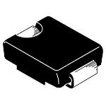
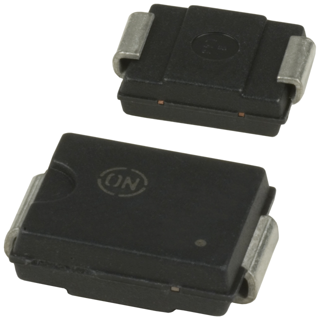
| 描述 | TVS DIODE 77.8VWM 125VC SMCTVS 二极管 - 瞬态电压抑制器 91V 1500W Unidirectional |
| 产品分类 | |
| 品牌 | ON Semiconductor |
| 产品手册 | |
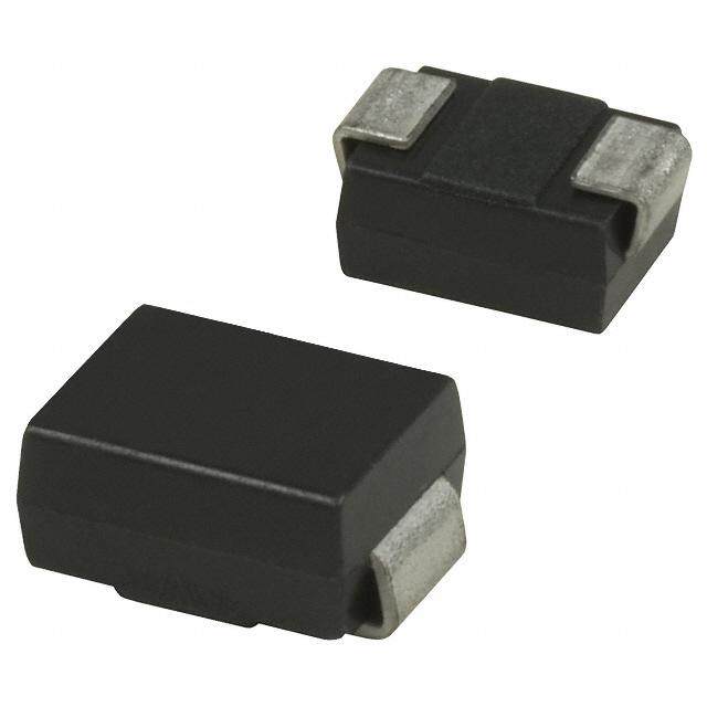
| 产品图片 |
|
| rohs | 符合RoHS无铅 / 符合限制有害物质指令(RoHS)规范要求 |
| 产品系列 | 二极管与整流器,TVS二极管,TVS 二极管 - 瞬态电压抑制器,ON Semiconductor 1.5SMC91AT3G- |
| 数据手册 | |
| 产品型号 | 1.5SMC91AT3G |
| 不同频率时的电容 | - |
| 产品目录页面 | |
| 产品种类 | Diodes- TVS |
| 供应商器件封装 | SMC |
| 其它名称 | 1.5SMC91AT3GOSCT |
| 击穿电压 | 86.5 V |
| 功率-峰值脉冲 | 1500W (1.5kW) |
| 包装 | 剪切带 (CT) |
| 单向通道 | 1 |
| 双向通道 | - |
| 商标 | ON Semiconductor |
| 安装类型 | 表面贴装 |
| 安装风格 | SMD/SMT |
| 封装 | Reel |
| 封装/外壳 | DO-214AB,SMC |
| 封装/箱体 | SMC |
| 尺寸 | 5.84 mm W x 6.86 mm L |
| 峰值浪涌电流 | 12 A |
| 峰值脉冲功率耗散 | 1500 W |
| 工作温度 | -65°C ~ 150°C (TJ) |
| 工作电压 | 77.8 V |
| 工厂包装数量 | 2500 |
| 应用 | 通用 |
| 最大工作温度 | + 150 C |
| 最小工作温度 | - 65 C |
| 极性 | Unidirectional |
| 标准包装 | 1 |
| 电压-击穿(最小值) | 86.5V |
| 电压-反向关态(典型值) | 77.8V |
| 电压-箝位(最大值)@Ipp | 125V |
| 电流-峰值脉冲(10/1000µs) | - |
| 电源线路保护 | 无 |
| 端接类型 | SMD/SMT |
| 类型 | 齐纳 |
| 系列 | 1.5SMC6.8AT3G |
| 钳位电压 | 125 V |


- 商务部:美国ITC正式对集成电路等产品启动337调查
- 曝三星4nm工艺存在良率问题 高通将骁龙8 Gen1或转产台积电
- 太阳诱电将投资9.5亿元在常州建新厂生产MLCC 预计2023年完工
- 英特尔发布欧洲新工厂建设计划 深化IDM 2.0 战略
- 台积电先进制程称霸业界 有大客户加持明年业绩稳了
- 达到5530亿美元!SIA预计今年全球半导体销售额将创下新高
- 英特尔拟将自动驾驶子公司Mobileye上市 估值或超500亿美元
- 三星加码芯片和SET,合并消费电子和移动部门,撤换高东真等 CEO
- 三星电子宣布重大人事变动 还合并消费电子和移动部门
- 海关总署:前11个月进口集成电路产品价值2.52万亿元 增长14.8%


PDF Datasheet 数据手册内容提取
TVS Diodes Surface Mount > 1500W > 1.5SMCxxAT3G 1.5SMCxxAT3G Pb Description The 1.5SMCxxAT3G series is designed to protect voltage sensitive components from high voltage, high energy transients. They have excellent clamping capability, high surge capability, low zener impedance and fast response time. This 1.5SMCxxAT3G series is provided in an SMC package ideally suited for small form factor requirements found in communication , automotive, process control, medical equipment and many other industrial and consumer applications. Features • Working Peak Reverse Voltage Range − 5.8 V to 78 V Maximum Ratings and Thermal Characteristics • Nominal Breakdown Voltage Range − 6.8 V to 91V Parameter Symbol Value Unit • Peak Power − 1500 W @ 1 ms Peak Power Dissipation (Note 1) @ TL = P 1500 W • ESD Rating of Class 3 (> 16 kV) per Human Body Model 25°C, Pulse Width = 1 ms PK • Low Leakage < 5 µA Above 10 V DC Power Dissipation @ T = 75°C Measured Zero Lead LengLth (Note 2) PD 4.0 W • Maximum Temperature Coefficient Specified Derate Above 75°C 54.6 mW/°C • Response Time is Typically < 1 ns Bi-directional TLheeadrmal Resistance from Junction−to− R JL 18.3 °C/W • Pb−Free Packages areB Aiv-daiilraebcleti onal DC Power Dissipation (Note 3) @ TA = PD 0.75 W 25°C Derate Above 25°C 6.1 mW/°C Functional Diagram Ttoh–e Armmabl iReenstistance from Junction– RθJA 165 °C/W Cathode Anode Cathode Anode Forward Surge Current (Note 4) I 200 A @ T = 25°C FSM A Operating and Storage T T -65 to °C Additional Information Uni-directional Temperature Range J, stg +150 Uni-directional Stresses exceeding Maximum Ratings may damage the component. Maximum Ratings are stress ratings only. Functional operation above the Recommended Operating Conditions is not implied. Extended exposure to stresses above the Recommended Operating Conditions Datasheet Resources Samples may affect component reliability. 1. 10 x 1000 µs, non−repetitive. 2. 1 in square copper pad, FR−4 board. 3. FR−4 board, using Littelfuse minimum recommended footprint, as shown in 403-03 case outline dimensions spec. 4. 1/2 sine wave (or equivalent square wave), PW = 8.3 ms, duty cycle = 4 pulses per minute maximum. © 2018 Littelfuse, Inc. Specifications are subject to change without notice. Revised: 02/23/18
TVS Diodes Surface Mount > 1500W > 1.5SMCxxAT3G I-V Curve Characteristics (T = 25°C unless otherwise noted, V = 3.5 V Max @ I = 100 A) (Note 5) A F F Symbol Parameter I I Maximum Reverse Peak Pulse Current PP V Clamping Voltage @ I C PP V Working Peak Reverse Voltage RWM I Maximum Reverse Leakage Current @ V V R RWM V Breakdown Voltage @ I BR T I Test Current T I Forward Current F V Forward Voltage @ I F F 5. 1/2 sine wave (or equivalent square wave), PW = 8.3 ms, non−repetitive duty cycle. © 2018 Littelfuse, Inc. Specifications are subject to change without notice. Revised: 02/23/18
TVS Diodes Surface Mount > 1500W > 1.5SMCxxAT3G Electrical Characteristics (T = 25°C unless otherwise noted) A V I @ Breakdown Voltage V @ I (Note 8) RWM R C PP MV BR Component* Component (Note 6) V Marking RWM V (V) (Note 6 & 7) @ I V I BR T C PP Volts µA MIN NOM MAX mA Volts Amps %/ C 1.5SMC6.8AT3G 6V8A 5.8 1000 6.45 6.8 7.14 10 10.5 143 0.057 1.5SMC7.5AT3G 7V5A 6.4 500 7.13 7.5 7.88 10 11.3 132 0.061 1.5SMC8.2AT3G 8V2A 7.02 200 7.79 8.2 8.61 10 12.1 124 0.065 1.5SMC10AT3G 10A 8.55 10 9.5 10 10.5 1 14.5 103 0.073 1.5SMC12AT3G 12A 10.2 5 11.4 12 12.6 1 16.7 90 0.078 1.5SMC13AT3G 13A 11.1 5 12.4 13 13.7 1 18.2 82 0.081 1.5SMC15AT3G 15A 12.8 5 14.3 15 15.8 1 21.2 71 0.084 1.5SMC16AT3G 16A 13.6 5 15.2 16 16.8 1 22.5 67 0.086 1.5SMC18AT3G 18A 15.3 5 17.1 18 18.9 1 25.2 59.5 0.088 1.5SMC20AT3G 20A 17.1 5 19 20 21 1 27.7 54 0.09 1.5SMC22AT3G 22A 18.8 5 20.9 22 23.1 1 30.6 49 0.092 1.5SMC24AT3G 24A 20.5 5 22.8 24 25.2 1 33.2 45 0.094 1.5SMC27AT3G 27A 23.1 5 25.7 27 28.4 1 37.5 40 0.096 1.5SMC30AT3G 30A 25.6 5 28.5 30 31.5 1 41.4 36 0.097 1.5SMC33AT3G 33A 28.2 5 31.4 33 34.7 1 45.7 33 0.098 1.5SMC36AT3G 36A 30.8 5 34.2 36 37.8 1 49.9 30 0.099 1.5SMC39AT3G 39A 33.3 5 37.1 39 41 1 53.9 28 0.1 1.5SMC43AT3G 43A 36.8 5 40.9 43 45.2 1 59.3 25.3 0.101 1.5SMC47AT3G 47A 40.2 5 44.7 47 49.4 1 64.8 23.2 0.101 1.5SMC51AT3G 51A 43.6 5 48.5 51 53.6 1 70.1 21.4 0.102 1.5SMC56AT3G 56A 47.8 5 53.2 56 58.8 1 77 19.5 0.103 1.5SMC62AT3G 62A 53 5 58.9 62 65.1 1 85 17.7 0.104 1.5SMC68AT3G 68A 58.1 5 64.6 68 71.4 1 92 16.3 0.104 1.5SMC75AT3G 75A 64.1 5 71.3 75 78.8 1 103 14.6 0.105 1.5SMC82AT3G 82A 70.1 5 77.9 82 86.1 1 113 13.3 0.105 1.5SMC91AT3G 91A 77.8 5 86.5 91 95.5 1 125 12 0.106 6. A transient suppressor is normally selected according to the maximum working peak reverse voltage (V ), which should be equal RWM to or greater than the DC or continuous peak operating voltage level. 7. V measured at pulse test current I at an ambient temperature of 25°C. BR T 8. Surge current waveform per Figure 2 and derate per Figure 3 of the General Data − 1500 Watt at the beginning of this group. © 2018 Littelfuse, Inc. Specifications are subject to change without notice. Revised: 02/23/18
TVS Diodes Surface Mount > 1500W > 1.5SMCxxAT3G Ratings and Characteristic Curves Figure 1. Pulse Rating Curve Figure 2. Pulse Waveform PULSE WIDTH (tP) IS DEFINED AS t≤ 10 s THAT POINT WHERE THE PEAK CURRENT DECAYS TO 50% OF 100 IPP. PEAK VALUE - IPP %) E ( U AL HALF VALUE - IPP V 2 50 tP 0 Figure 3. Pulse Derating Curve Figure 4. Dynamic Impedance 160 C °5 140 F2 N % O@ T= A 120 G IT NN 100 ULSE DERATIER OR CURRE 8600 PW PEAK K PO 40 A 20 E P 0 0 25 50 75 100 125 150 ° © 2018 Littelfuse, Inc. Specifications are subject to change without notice. Revised: 02/23/18
TVS Diodes Surface Mount > 1500W > 1.5SMCxxAT3G Dimensions Soldering Footrpint HE E bD D mm inches A ORDERING INFORMATION L L1 c A1 Component Package Shipping Inches Millimeters SMC 2,500 / Dim 1SMCxxAT3G Min Nom Max Min Nom Max (Pb−Free) Tape & Reel A 0.075 0.084 0.095 1.90 2.13 2.41 A1 0.002 0.004 0.006 0.05 0.10 0.15 b 0.115 0.118 0.121 2.92 3.00 3.07 c 0.006 0.009 0.012 0.15 0.23 0.30 Flow/Wave Soldering (Solder Dipping) D 0.220 0.230 0.240 5.59 5.84 6.10 Peak Temperature : 260OC E 0.260 0.270 0.280 6.60 6.86 7.11 Dipping Time : 10 seconds H 0.305 0.313 0.320 7.75 7.94 8.13 E L 0.030 0.040 0.050 0.76 1.02 1.27 L1 0.020 REF 0.51 REF Physical Specifications NOTES Void-free, transfer-molded, thermosetting 1. DIMENSIONING AND TOLERANCING PER ANSI Y14.5M, 1982. Case plastic 2. CONTROLLING DIMENSION: INCH. 3. D DIMENSION SHALL BE MEASURED WITHIN DIMENSION P. Polarity Cathode indicated by polarity band 4. 403-01 THRU -02 OBSOLETE, NEW STANDARD 403-03. Part Marking System Mounting Position Any All external surfaces are corrosion Finish resistant and leads are readily solderable Modified L−Bend providing more contact Leads area to bond pads Specific Component Code Disclaimer Notice - Information furnished is believed to be accurate and reliable. However, users should independently evaluate the suitability of and test each product selected for their own applications. Littelfuse products are not designed for, and may not be used in, all applications. Read complete Disclaimer Notice at: www.littelfuse.com/disclaimer-electronics. © 2018 Littelfuse, Inc. Specifications are subject to change without notice. Revised: 02/23/18