 Datasheet下载
- 型号: 06035C472KAT2A
- 制造商: AVX
- 库位|库存: xxxx|xxxx
- 要求:
| 数量阶梯 | 香港交货 | 国内含税 |
| +xxxx | $xxxx | ¥xxxx |
查看当月历史价格
查看今年历史价格
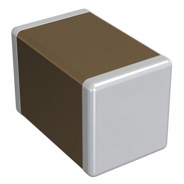
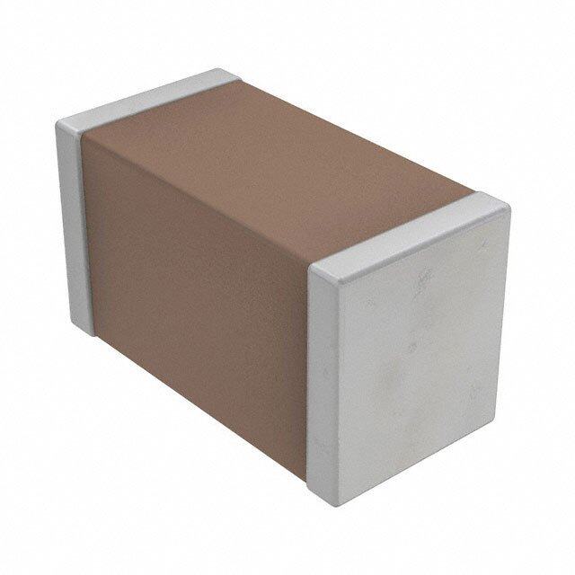
06035C472KAT2A产品简介:
ICGOO电子元器件商城为您提供06035C472KAT2A由AVX设计生产,在icgoo商城现货销售,并且可以通过原厂、代理商等渠道进行代购。 06035C472KAT2A价格参考¥0.05-¥0.05。AVX06035C472KAT2A封装/规格:陶瓷电容器, 4700pF ±10% 50V 陶瓷电容器 X7R 0603(1608 公制)。您可以下载06035C472KAT2A参考资料、Datasheet数据手册功能说明书,资料中有06035C472KAT2A 详细功能的应用电路图电压和使用方法及教程。
AVX Corporation的06035C472KAT2A是一款陶瓷电容器,具有广泛的电子应用场景。这款电容器属于多层片式陶瓷电容器(MLCC),尺寸为0603英寸(1608公制),容量为470pF,容差为±10%(K级),额定电压为50V。

 应用场景:

1. 电源滤波:
   - 该电容器常用于电源电路中的滤波,帮助去除电源中的纹波和噪声,确保输出电压的稳定性。它特别适用于高频电源转换器、开关电源等设备中,能够有效抑制高频噪声,提高电源的质量和可靠性。

2. 去耦和旁路:
   - 在数字电路和模拟电路中,06035C472KAT2A可以作为去耦电容或旁路电容使用。它可以帮助消除集成电路(IC)内部的瞬态电流波动,减少电源线上的噪声,确保信号的完整性。尤其在高速数字电路中,这种电容器能够提供快速的响应时间,有效抑制高频噪声。

3. 射频(RF)电路:
   - 由于其低ESR(等效串联电阻)和高自谐振频率,这款电容器非常适合用于射频电路中。它可以用于匹配网络、滤波器、谐振电路等,帮助优化射频信号的传输性能,减少信号损失和干扰。

4. 振荡电路:
   - 在振荡电路中,06035C472KAT2A可以用作定时元件,帮助设定振荡频率。它的稳定性和精度使其成为时钟电路、晶体振荡器等应用的理想选择。

5. 耦合与隔直:
   - 在音频放大器和其他信号处理电路中,该电容器可以用于耦合不同级之间的信号,同时隔离直流成分,防止直流偏置影响后续电路的工作。

6. 温度补偿:
   - 由于其采用了C0G(NP0)介质材料,具有极佳的温度稳定性,适合用于需要精确电容值且对温度变化敏感的应用场合,如精密测量仪器、传感器接口等。

7. 表面贴装技术(SMT):
   - 该电容器采用表面贴装封装,适用于自动化生产线,广泛应用于各种消费电子产品、通信设备、工业控制等领域。

总之,AVX Corporation的06035C472KAT2A陶瓷电容器凭借其优异的电气特性和可靠性,广泛应用于各类电子设备中,特别是在高频、高精度要求的场景下表现出色。
| 参数 | 数值 |
| 产品目录 | |
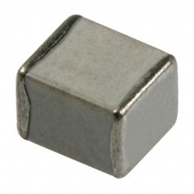
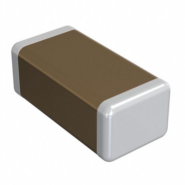
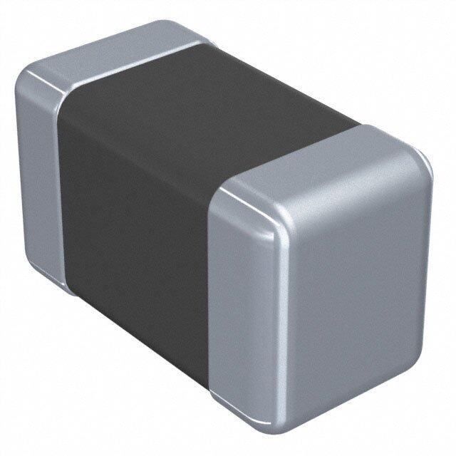
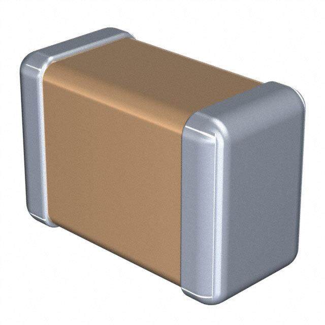
| 描述 | CAP CER 4700PF 50V 10% X7R 0603多层陶瓷电容器MLCC - SMD/SMT 50volts 4700pF 10% X7R |
| 产品分类 | |
| 品牌 | AVX |
| 产品手册 | |
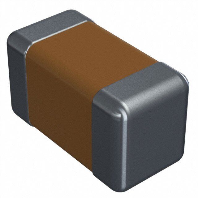
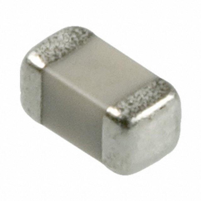
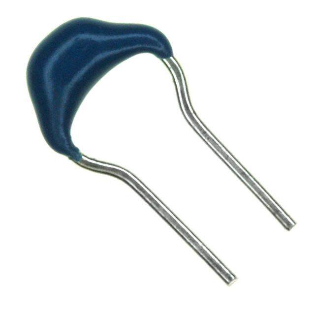
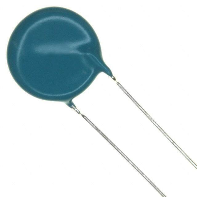
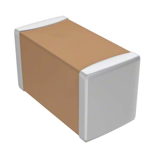
| 产品图片 |
|
| rohs | RoHS 合规性豁免无铅 / 符合限制有害物质指令(RoHS)规范要求 |
| 产品系列 | MLCC,多层陶瓷电容器MLCC - SMD/SMT,AVX 06035C472KAT2A- |
| 数据手册 | |
| 产品型号 | 06035C472KAT2A |
| 产品 | General Type MLCCs |
| 产品培训模块 | http://www.digikey.cn/PTM/IndividualPTM.page?site=cn&lang=zhs&ptm=21795 |
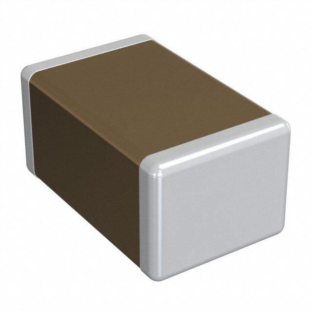
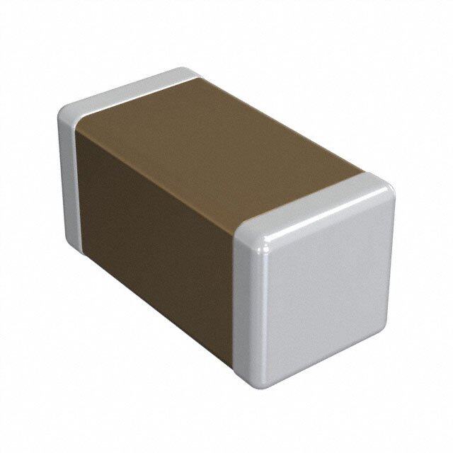
| 产品目录绘图 |
|
| 产品目录页面 | |
| 产品种类 | 多层陶瓷电容器MLCC - SMD/SMT |
| 其它名称 | 06035C472KAT2A/4K |
| 包装 | 带卷 (TR) |
| 厚度(最大值) | 0.035"(0.90mm) |
| 商标 | AVX |
| 外壳代码-in | 0603 |
| 外壳代码-mm | 1608 |
| 外壳宽度 | 0.81 mm |
| 外壳长度 | 1.6 mm |
| 外壳高度 | 0.9 mm |
| 大小/尺寸 | 0.063" 长 x 0.032" 宽(1.60mm x 0.81mm) |
| 安装类型 | 表面贴装,MLCC |
| 容差 | 10 % |
| 封装 | Reel |
| 封装/外壳 | 0603(1608 公制) |
| 封装/箱体 | 0603 (1608 metric) |
| 工作温度 | -55°C ~ 125°C |
| 工作温度范围 | - 55 C to + 125 C |
| 工厂包装数量 | 4000 |
| 应用 | 通用 |
| 引线形式 | - |
| 引线间距 | - |
| 损耗因数DF | 2.5 |
| 最大工作温度 | + 125 C |
| 最小工作温度 | - 55 C |
| 标准包装 | 4,000 |
| 温度系数 | X7R |
| 温度系数/代码 | +/- 15 % |
| 特性 | - |
| 电介质 | X7R |
| 电压-额定 | 50V |
| 电压额定值 | 50 V |
| 电压额定值DC | 50 V |
| 电容 | 4700 pF |
| 端接类型 | SMD/SMT |
| 等级 | - |
| 类型 | Commercial Surface Mount Chip |
| 系列 | 0603 C |
| 高度-安装(最大值) | - |


- 商务部:美国ITC正式对集成电路等产品启动337调查
- 曝三星4nm工艺存在良率问题 高通将骁龙8 Gen1或转产台积电
- 太阳诱电将投资9.5亿元在常州建新厂生产MLCC 预计2023年完工
- 英特尔发布欧洲新工厂建设计划 深化IDM 2.0 战略
- 台积电先进制程称霸业界 有大客户加持明年业绩稳了
- 达到5530亿美元!SIA预计今年全球半导体销售额将创下新高
- 英特尔拟将自动驾驶子公司Mobileye上市 估值或超500亿美元
- 三星加码芯片和SET,合并消费电子和移动部门,撤换高东真等 CEO
- 三星电子宣布重大人事变动 还合并消费电子和移动部门
- 海关总署:前11个月进口集成电路产品价值2.52万亿元 增长14.8%

PDF Datasheet 数据手册内容提取
X7R Dielectric General Specifications X7R formulations are called “temperature stable” ceramics and fall into EIA Class II materials. X7R is the most popular of these intermediate dielectric constant materials. Its temperature variation of capacitance is within ±15% from -55°C to +125°C. This capacitance change is non-linear. Capacitance for X7R varies under the influence of electrical operating con-ditions such as voltage and frequency. X7R dielectric chip usage covers the broad spectrum of industrial applications where known changes in capacitance due to applied voltages are acceptable. PART NUMBER (see page 2 for complete part number explanation) 0805 5 C 103 M A T 2 A Size Voltage Dielectric Capacitance Capacitance Failure Terminations Packaging Special (L” x W”) 4V = 4 X7R = C Code (In pF) Tolerance Rate T = Plated Ni and Sn 2 = 7” Reel Code 2 Sig. Digits + A = Not 7 = Gold Plated* 4 = 13” Reel A = Std. 6.3V = 6 J = ± 5%* Number of Zeros Applicable Z= FLEXITERM®** Product 10V = Z K = ±10% Contact 16V = Y M = ± 20% *Optional termination Factory For 25V = 3 Multiples 50V = 5 *≤1µF only, **See FLEXITERM® X7R section 100V = 1 contact factory for 200V = 2 additional values 500V = 7 NOTE: Contact factory for availability of Termination and Tolerance Options for Specific Part Numbers. Contact factory for non-specified capacitance values. 042718 1199
X7R Dielectric C0G (NP0) Dielectric Specifications and Test Methods Specifications and Test Methods Parameter/Test X7R Specification Limits Measuring Conditions Operating Temperature Range -55ºC to +125ºC Temperature Cycle Chamber PaCraapamcietatnecre/Test NPW0it hSinp sepcecififiiecda ttoiloerna nLceimits Measuring Conditions Operating Temperature Range -55ºC to +125ºC TemFrpeeqr.:a 1tu.0re k HCzy c±l e1 0C%hamber ≤ 10% for ≥ 50V DC rating≤ 12.5% for 25V DC rating Voltage: 1.0Vrms ± .2V DisCsiappataiocni tFaanctcoer ≤ 12.5W%i tfhoirn 2 s5pVe cainfide d1 6toVl eDrCan rcaeting Fre Fqo.:r 1C.a0p M >H 1z0 µ±F 1, 005%V rfmor @ca p12 ≤0 H1z000 pF <30 pF: Q≥ 400+20 x Cap Value 1.0 kHz ± 10% for cap > 1000 pF Q ≤ 12.5% for ≤ 10V DC rating ≥30 pF: Q≥ 1000 Voltage: 1.0Vrms ± .2V Insulation Resistance 110000,0,00000MMΩΩ o or r1 010000M0MΩ Ω- µ- Fµ,F, CChhaargreg ed edveivceic ew iwthi trha treadte vdo lvtaogltea gfoer for Insulation Resistance wwhhicihcehveevre irs i sle lsesss 16200 ±± 55 sseeccss @ @ r orooomm te tmemp/ph/uhmumidiitdyity CChhaargrgee d deveivciec ew withit h2 5205%0 %of oraf treadte vdo lvtaogltea gfoer for DDiieelleeccttrirci cS tSretnrgetnhgth NNoo b brereaakkddoowwn no ro vr ivsuisaul adle dfeecfetscts 11--55 s seeccoonnddss, ,w w/c/hcahragreg ea nadn ddi sdcishcahrgaerg ceu rcruernrtent limlimiteitde dto t o50 5 m0 Am (Am (amx)ax) NNootete: :C Chahragreg ed edveicveic we iwthi t1h5 105%0 %of roaft eradted vovlotaltgaeg efo fro 5r0 500V0 dVe dveicveisc.es. AApppepaeraarnacnece NNo od edfeefcetcsts DDefleefcleticotnio: n2:m 2mmm RReessiisstatanncec teo to CC aVpaVaaparciaariicttaaiiottnianocnnece ±5% or ±.5 p≤F ,± w12h%ichever is greater TTeests Tt iTmime:e 3: 03 0se sceocnodnsds SSFFttlrlereeexsxussuresesrees Di sFsaipcaQtotiron MMeeeetsts I nInitiiatial Vl aVlauleuse s(A (sA As bAobvoev)e) InIsnuslualtaiotnion ≥≥ I nIintiiatila Vl aVlauleu ex 0x. 30.3 RReseissitsatnacnece ≥≥ 9955%% o of fe eaachch te tremrminianla slh sohuoldu lbde b ceo cveorveedred DDipip d deevviciece in i ne uetuetcetcict isco sldoeldr eart a2t3 203 ±0 5 ±ºC 5ºC SSooldlderearbailbityility wwithith fr fersehs hs oslodledrer fofor r5 5.0. 0± ±0 .05. 5se sceocnodnsds Appearance No defects, <25% leaching of either end terminal Appearance No defects, <25% leaching of either end terminal Capacitance Capacitance ≤ ±2.5% or ±.2≤5 ± p7F.5, %whichever is greater Variation Variation Dip deDvipic ed einv iecuet einc teicu steocldteicr saot l2d6e0r ºaCt f2o6r 06º0Cs efocor n6d0s. RReessiisstatanncec teo to DissipaQtion MMeeeetsts I nInitiiatial Vl aVlauleuse s(A (sA As bAobvoev)e) Stosree caot nrdoso.m S tteomrep aetr arotuorme ftoerm 2p4e ±ra 2tuhroeu frosr b 2e4fo ±re 2 SSoollddeer rH Heaetat IFnascutloartion hours mbeefaosruer imnge ealseucrtirnicga le plerocptreicratiel sp.roperties. Insulation Meets Initial Values (As Above) Resistance Meets Initial Values (As Above) Resistance Dielectric Dielectric Meets Initial Values (As Above) Strength Meets Initial Values (As Above) Strength Appearance No visual defects Step 1: -55ºC ± 2º 30 ± 3 minutes Appearance No visual defects Step 1: -55ºC ± 2º 30 ± 3 minutes Capacitance ≤ ±2.5% or ±.25 pF, whichever is greater Step 2: Room Temp ≤ 3 minutes CapVaacriitaatniocne ≤ ±7.5% Step 2: Room Temp ≤ 3 minutes Variation Thermal Q Meets Initial Values (As Above) Step 3: +125ºC ± 2º 30 ± 3 minutes Dissipation Thermal Meets Initial Values (As Above) Step 3: +125ºC ± 2º 30 ± 3 minutes SShhoockck IFnascutloartion Meets Initial Values (As Above) Step 4: Room Temp ≤ 3 minutes IRnseuslaisttioannce Meets Initial Values (As Above) Step 4: Room Temp ≤ 3 minutes ReDsiisetlaencctreic Repeat for 5 cycles and measure after Meets Initial Values (As Above) DiSelterecntrgict h 24 hoRuresp aeat tr ofoorm 5 tceymclpees raantudr emeasure after Meets Initial Values (As Above) ASptrpeenagrtahnce No visual defects 24 ± 2 hours at room temperature ACppaepaarcaintacnece No visual defects ≤ ±3.0% or ± .3 pF, whichever is greater Charge device with 1.5 rated voltage (≤ 10V) in CapVaacriitaatniocne ≤ ±12.5% test cChhamarbgeer dseevt iacet 1w2i5thºC tw ±ic 2eº Cra ftoerd 1v0o0lt0a gheo uinrs VariatQion ≥ 30 pF: Q≥ 350 test chamb(+e4r 8s,e -t0 a)t 125ºC ± 2ºC Load Life (CD=isNsiopmatiinoanl Cap) ≥10 p≤F ,I n<it3ia0l VpFal:ue x 2Q.0≥ (2S7e5e +A5bCov/2e) for 1000 hours (+48, -0). Load Life Factor <10 pF: Q≥ 200 +10C If RV > 10V then Life Test voltage will be 2xRV Insulation but tRheerme oavree efrxocme ptteiosnt sc h(palmeabseer aconndt asctat bAiVlizXe faotr IRnseuslaisttioannce ≥≥ I nInitiitaial Vl Valauleu ex x0 .03. 3(S (eSee Aeb Aobvoev)e) furortohmer t deemtapielsr aotnu reex fcoerp 2ti4o nhso)urs Resistance Dielectric Remove from tesbt ecfhoarme bmeer aasnudr isntgab.ilize at room Dielectric Meets Initial Values (As Above) Strength Meets Initial Values (As Above) temperature for 24 ± 2 hours before measuring. Strength Appearance No visual defects ACppaepaarcaintacnece No visual defects ≤ ±5.0% or ± .5 pF, whichever is greater Store in a test chamber set at 85ºC ± 2ºC/ CapVaacriitaatniocne ≤ ±12.5% 85S%to ±re 5 i%n ar etelasttiv ceh haummbiedrit ys efot ra t1 8050º0C h ±ou 2rsºC / Variation ≥ 30 pF: Q≥ 350 85% ± 5% relative humidity for 1000 hours (+48, -0) with rated voltage applied. LLooaadd DissipaQtion ≥10 pF, <30 pF: Q≥ 275 +5C/2 (+48, -0) with rated voltage applied. ≤ Initial Value x 2.0 (See Above) HHuummidiidtyity Factor <10 pF: Q≥ 200 +10C Remove from chamber and stabilize at room Insulation Remove from chamber and stabilize at Insulation ≥≥ I nInitiitaial Vl Valauleu ex x0 .03. 3(S (eSee Aeb Aobvoev)e) temperature and humidity for RReseissitsatnacnece room temperature for 24 ± 2 hours 24 ± 2 hours before measuring. Dielectric before measuring. DiSelterecntrgict h MMeeeetsts I nInitiiatial Vl aVlauleuse s(A (sA As bAobvoev)e) Strength 22 00 042718 100917 5
X7R Dielectric Capacitance Range PREFERRED SIZES ARE SHADED SIZE 0101* 0201 0402 0603 0805 1206 Soldering Reflow Only Reflow Only Reflow/Wave Reflow/Wave Reflow/Wave Reflow/Wave Packaging Paper/Embossed All Paper All Paper All Paper Paper/Embossed Paper/Embossed mm 0.40 ± 0.02 0.60 ± 0.03 1.00 ± 0.10 1.60 ± 0.15 2.01 ± 0.20 3.20 ± 0.20 (L) Length (in) (0.016 ± 0.0008) (0.024 ± 0.001) (0.040 ± 0.004) (0.063 ± 0.006) (0.079 ± 0.008) (0.126 ± 0.008) mm 0.20 ± 0.02 0.30 ± 0.03 0.50 ± 0.10 0.81 ± 0.15 1.25 ± 0.20 1.60 ± 0.20 (W) Width (in) (0.008 ± 0.0008) (0.011 ± 0.001) (0.020 ± 0.004) (0.032 ± 0.006) (0.049 ± 0.008) (0.063 ± 0.008) mm 0.10± 0.04 0.15 ± 0.05 0.25 ± 0.15 0.35 ± 0.15 0.50 ± 0.25 0.50 ± 0.25 (t) Terminal (in) (0.004 ± 0.0016) (0.006 ± 0.002) (0.010 ± 0.006) (0.014 ± 0.006) (0.020 ± 0.010) (0.020 ± 0.010) WVDC 16 6.3 10 16 25 50 6.3 10 16 25 50 6.310 16 25 50 100200250 6.3 10 16 25 50 1002002506.3 10 16 25 50100200250500 Cap 100101 B A A A A A C C C G G G (pF) 150151 B A A A A A C C C G G G 220221 B A A A A A C C C G G G E E E E E E E 330331 B A A A A A C C C G G G J J J J J J K 470471 B A A A A A C C C G G G J J J J J J K 680681 B A A A A C C C G G G J J J J J J K 1000102 B A A A A C C C C G G G G J J J J J J J J K 1500152 B A A A A C C C C G G J G J J J J J J J J J J J J J J M 2200222 B A A A A C C C C G G J G J J J J J J J J J J J J J J M 3300332 A A A A C C C C G G J G J J J J J J J J J J J J J J M 4700472 A A A A C C C C G G J G J J J J J J J J J J J J J J M 6800682 A A A A C C C C G G J G J J J J J J J J J J J J J J P Cap 0.01103 A A A A C C C C G G G J G J J J J J J J J J J J J J J P (µF) 0.015153 C C C C G G G J J J J J J J N J J J J J M J Q 0.022223 C C C C G G G J J J J J N N J J J J J M J Q 0.033333 C C C C G G J J J J J N N N J J J J J M J Q 0.047473 C C C C G G G J J J J J N N N J J J J J M M 0.068683 C C C C G G G J J J J J N N J J J J J P M 0.1104 C C C C G G G G J J J J J N N J J J J P P P 0.15154 G G G G J J J J N N J J J J Q Q Q 0.22224 C C C G G J J J J J N N N J J J J Q Q Q 0.33334 J J J J J N N N N N J J M P Q 0.47474 C C J J J J J N N N N N M M M P Q 0.68684 J J J N N N M M 1.0105 C J J J J J N N N N M M 2.2225 J J J P P P P** Q Q Q Q Q** 4.7475 J P P P Q Q Q Q 10106 P P P Q Q X X 22226 Q Q Q 47476 Q Q 100107 WVDC 16 6.3 10 16 25 50 6.3 10 16 25 50 6.310 16 25 50 100200250 6.3 10 16 25 50 1002002506.3 10 16 25 50100200250500 SIZE 0101 0201 0402 0603 0805 1206 Letter A B C E G J K M N P Q X Y Z Max. 0.33 0.22 0.56 0.71 0.90 0.94 1.02 1.27 1.40 1.52 1.78 2.29 2.54 2.79 Thickness (0.013) (0.009) (0.022) (0.028) (0.035) (0.037) (0.040) (0.050) (0.055) (0.060) (0.070) (0.090) (0.100) (0.110) PAPER EMBOSSED NOTE: Contact factory for non-specified capacitance values *EIA 01005 **Contact Factory for Specifications 21 032519
X7R Dielectric Capacitance Range PREFERRED SIZES ARE SHADED SIZE 1210 1812 1825 2220 2225 Soldering Reflow Only Reflow Only Reflow Only Reflow Only Reflow Only Packaging Paper/Embossed All Embossed All Embossed All Embossed All Embossed mm 3.30 ± 0.4 4.50 ± 0.30 4.50 ± 0.30 5.70 ± 0.40 5.72 ± 0.25 (L) Length (in.) (0.130± 0.016) (0.177 ± 0.012) (0.177 ± 0.012) (0.225 ± 0.016) (0.225 ± 0.010) mm 2.50 ± 0.20 3.20 ± 0.20 6.40 ± 0.40 5.00 ± 0.40 6.35 ± 0.25 (W) Width (in.) (0.098 ± 0.008) (0.126 ± 0.008) (0.252 ± 0.016) (0.197 ± 0.016) (0.250 ± 0.010) mm 0.50 ± 0.25 0.61 ± 0.36 0.61 ± 0.36 0.64 ± 0.39 0.64 ± 0.39 (t) Terminal (in.) (0.020 ± 0.010) (0.024 ± 0.014) (0.024 ± 0.014) (0.025 ± 0.015) (0.025 ± 0.015) WVDC 10 16 25 50 100 200 500 16 25 50 100 200 500 50 100 200 25 50 100 200 500 50 100 200 Cap 100 101 (pF) 150 151 220 221 330 331 470 471 680 681 1000 102 1500 152 J J J J J J M 2200 222 J J J J J J M 3300 332 J J J J J J M 4700 472 J J J J J J M 6800 682 J J J J J J M Cap 0.01 103 J J J J J J M K K K K K M M M X X X X M P P (µF) 0.015 153 J J J J J J P K K K K P M M M X X X X M P P 0.022 223 J J J J J J Q K K K K P M M M X X X X M P P 0.033 333 J J J J J J Q K K K K X M M M X X X X M P P 0.047 473 J J J J J J Q K K K K Z M M M X X X X M P P 0.058 683 J J J J J M Q K K K K Z M M M X X X X M P P 0.1 104 J J J J J M X K K K K Z M M M X X X X M P P 0.15 154 J J J J M Z K K K P Z M M M X X X X M P X 0.22 224 J J J J P Z K K K P Z M M M X X X X M P X 0.33 334 J J J J Q K K M X M M X X X X M P X 0.47 474 M M M M Q K K P X M M X X X X M P X 0.68 684 M M P X X M M Q M P X X M P X 1.0 105 N N P X Z M M X Z M P X X M P X 1.5 155 N N Z Z Z Z Z Z Q X X M X Z 2.2 225 X X Z Z Z Z Z Z X X M X Z 3.3 335 X X Z Z Z Z Z Z X Z 4.7 475 Z Z Z Z Z Z Z X Z 10 106 Z Z Z Z Z Z Z 22 226 Z Z Z Z 47 476 Z 100 107 WVDC 10 16 25 50 100 200 500 16 25 50 100 200 500 50 100 200 25 50 100 200 500 50 100 200 SIZE 1210 1812 1825 2220 2225 Letter A B C E G J K M N P Q X Y Z Max. 0.33 0.22 0.56 0.71 0.90 0.94 1.02 1.27 1.40 1.52 1.78 2.29 2.54 2.79 Thickness (0.013) (0.009) (0.022) (0.028) (0.035) (0.037) (0.040) (0.050) (0.055) (0.060) (0.070) (0.090) (0.100) (0.110) PAPER EMBOSSED NOTE: Contact factory for non-specified capacitance values 22 101618