ICGOO在线商城 > 开发板,套件,编程器 > 配件 > MA320012
 Datasheet下载
- 型号: MA320012
- 制造商: Microchip
- 库位|库存: xxxx|xxxx
- 要求:
| 数量阶梯 | 香港交货 | 国内含税 |
| +xxxx | $xxxx | ¥xxxx |
查看当月历史价格
查看今年历史价格
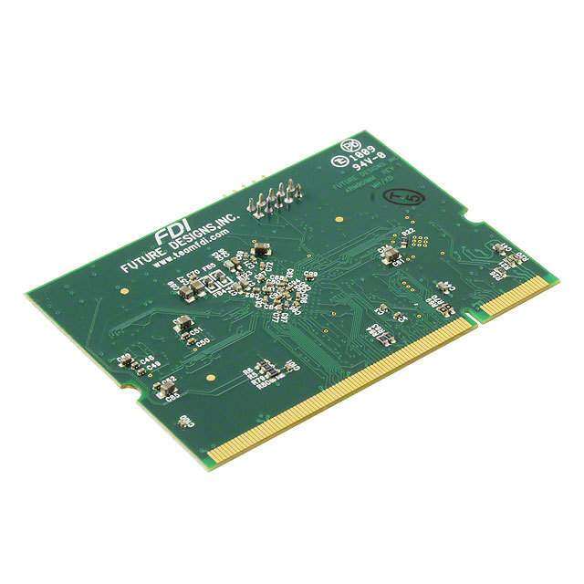
MA320012产品简介:
ICGOO电子元器件商城为您提供MA320012由Microchip设计生产,在icgoo商城现货销售,并且可以通过原厂、代理商等渠道进行代购。 MA320012价格参考。MicrochipMA320012封装/规格:配件, PIC32MZ2048ECH100 - 插拔式模块(PIM)。您可以下载MA320012参考资料、Datasheet数据手册功能说明书,资料中有MA320012 详细功能的应用电路图电压和使用方法及教程。
| 参数 | 数值 |
| 产品目录 | 编程器,开发系统嵌入式解决方案 |
| 描述 | MOD PIM PIC32MZ2048EC 100PIN子卡和OEM板 PIC32MZ2048EC Plug In Module |
| 产品分类 | |
| 品牌 | Microchip Technology |
| 产品手册 | http://www.microchip.com/stellent/idcplg?IdcService=SS_GET_PAGE&nodeId=1406&dDocName=en566641 |
| 产品图片 | |
| rohs | 符合RoHS无铅 / 符合限制有害物质指令(RoHS)规范要求 |
| 产品系列 | 嵌入式开发工具,嵌入式工具与配件,子卡和OEM板,Microchip Technology MA320012- |
| mouser_ship_limit | 此产品可能需要其他文件才能从美国出口。 |
| 数据手册 | http://www.microchip.com/mymicrochip/filehandler.aspx?ddocname=en566815 |
| 产品型号 | MA320012 |
| 产品 | Plug-In Modules |
| 产品种类 | 子卡和OEM板 |
| 商标 | Microchip Technology |
| 封装 | Bulk |
| 工具用于评估 | PIC32MZ EC PIM |
| 接口类型 | CAN, Ethernet, USB |
| 描述/功能 | PIC32MZ embedded connectivity (EC) 100-pin to 100-pin plug-in module |
| 标准包装 | 1 |
| 用于 | PIC32 MZ Series |
| 配件类型 | 插拔式模块(PIM) - PIC32MZ2048ECH100 |
| 配套使用产品/相关产品 | Microchip 开发板 |


- 商务部:美国ITC正式对集成电路等产品启动337调查
- 曝三星4nm工艺存在良率问题 高通将骁龙8 Gen1或转产台积电
- 太阳诱电将投资9.5亿元在常州建新厂生产MLCC 预计2023年完工
- 英特尔发布欧洲新工厂建设计划 深化IDM 2.0 战略
- 台积电先进制程称霸业界 有大客户加持明年业绩稳了
- 达到5530亿美元!SIA预计今年全球半导体销售额将创下新高
- 英特尔拟将自动驾驶子公司Mobileye上市 估值或超500亿美元
- 三星加码芯片和SET,合并消费电子和移动部门,撤换高东真等 CEO
- 三星电子宣布重大人事变动 还合并消费电子和移动部门
- 海关总署:前11个月进口集成电路产品价值2.52万亿元 增长14.8%

PDF Datasheet 数据手册内容提取
Not recommended for new designs – Please use the PIC32MZ Embedded Connectivity with Floating Point Unit (EF) Family PIC32MZ Embedde d Connectivity (EC) Family 32-bit MCUs (up to 2 MB Live-Update Flash and 512 KB SRAM) with Audio and Graphics Interfaces, HS USB, Ethernet, and Advanced Analog Operating Conditions Advanced Analog Features • 2.3V to 3.6V, -40ºC to +85ºC, DC to 200 MHz • 10-bit ADC resolution and up to 48 analog inputs • Flexible and independent ADC trigger sources Core: 200 MHz (up to 330 DMIPS) microAptiv™ • Two comparators with 32 programmable voltage references • 16 KB I-Cache, 4 KB D-Cache • Temperature sensor with ±2ºC accuracy • MMU for optimum embedded OS execution Communication Interfaces • microMIPS™ mode for up to 35% smaller code size • DSP-enhanced core: • Two CAN modules (with dedicated DMA channels): - Four 64-bit accumulators - 2.0B Active with DeviceNet™ addressing support - Single-cycle MAC, saturating and fractional math • Six UART modules (25 Mbps): • Code-efficient (C and Assembly) architecture - Supports LIN 1.2 and IrDA® protocols • Six 4-wire SPI modules Clock Management • SQI configurable as an additional SPI module (50 MHz) • Internal oscillator • Five I2C modules (up to 1 Mbaud) with SMBus support • Programmable PLLs and oscillator clock sources • Parallel Master Port (PMP) • Fail-Safe Clock Monitor (FSCM) • Peripheral Pin Select (PPS) to enable function remap • Independent Watchdog Timers (WDT) and Deadman Timers/Output Compare/Input Capture Timer (DMT) • Fast wake-up and start-up • Nine 16-bit or up to four 32-bit timers/counters • Nine Output Compare (OC) modules Power Management • Nine Input Capture (IC) modules • Low-power modes (Sleep and Idle) • PPS to enable function remap • Integrated Power-on Reset and Brown-out Reset • Real-Time Clock and Calendar (RTCC) module Memory Interfaces Input/Output • 50 MHz External Bus Interface (EBI) • 5V-tolerant pins with up to 32 mA source/sink • 50 MHz Serial Quad Interface (SQI) • Selectable open drain, pull-ups, and pull-downs Audio and Graphics Interfaces • External interrupts on all I/O pins • Graphics interfaces: EBI or PMP Qualification and Class B Support • Audio data communication: I2S, LJ, and RJ • Class B Safety Library, IEC 60730 • Audio control interfaces: SPI and I2C • Back-up internal oscillator • Audio master clock: Fractional clock frequencies with USB synchronization Debugger Development Support High-Speed (HS) Communication Interfaces • In-circuit and in-application programming • 4-wire MIPS® Enhanced JTAG interface (with Dedicated DMA) • Unlimited software and 12 complex breakpoints • USB 2.0-compliant Hi-Speed On-The-Go (OTG) controller • IEEE 1149.2-compatible (JTAG) boundary scan • 10/100 Mbps Ethernet MAC with MII and RMII interface • Non-intrusive hardware-based instruction trace Security Features Software and Tools Support • Crypto Engine with a RNG for data encryption/decryption • C/C++ compiler with native DSP/fractional support and authentication (AES, 3DES, SHA, MD5, and HMAC) • MPLAB® Harmony Integrated Software Framework • Advanced memory protection: • TCP/IP, USB, Graphics, and mTouch™ middleware - Peripheral and memory region access control • MFi, Android™, and Bluetooth® audio frameworks Direct Memory Access (DMA) • RTOS Kernels: Express Logic ThreadX, FreeRTOS™, • Eight channels with automatic data size detection OPENRTOS®, Micriµm® µC/OS™, and SEGGER embOS® • Programmable Cyclic Redundancy Check (CRC) Packages Type QFN TQFP VTLA LQFP Pin Count 64 64 100 144 124 144 I/O Pins (up to) 53 53 78 120 98 120 Contact/Lead Pitch 0.50 mm 0.50 mm 0.40 mm 0.50 mm 0.40 mm 0.50 mm 0.50 mm Dimensions 9x9x0.9 mm 10x10x1 mm 12x12x1 mm 14x14x1 mm 16x16x1 mm 9x9x0.9 mm 20x20x1.40 mm 2013-2016 Microchip Technology Inc. DS60001191G-page 1
D TABLE 1: PIC32MZ EC FAMILY FEATURES P S 60 I 0 Remappable Peripherals s C 01191G-page 2 Device Program Memory (KB) Data Memory (KB) Pins Packages Boot Flash Memory (KB) Remappable Pins Timers/Capture/(1)Compare UART 2SPI/IS External (2)Interrupts CAN 2.0B Crypto RNG DMA Channels(Programmable/Dedicated) ADC (Channels) Analog Comparator USB 2.0 HS OTG 2IC PMP EBI SQI RTCC Ethernet I/O Pins JTAG Trace 32MZ E PIC32MZ1024ECG064 0 N Y 8/12 m PIC32MZ1024ECH064 1024 2 N Y 8/16 b PIC32MZ1024ECM064 TQFP, 2 Y Y 8/18 PIC32MZ2048ECG064 512 64 QFN 160 34 9/9/9 6 4 5 0 N Y 8/12 24 2 Y 4 Y N Y Y Y 46 Y Y e d PIC32MZ2048ECH064 2048 2 N Y 8/16 d PIC32MZ2048ECM064 2 Y Y 8/18 e PIC32MZ1024ECG100 0 N Y 8/12 d PIC32MZ1024ECH100 1024 2 N Y 8/16 PIC32MZ1024ECM100 2 Y Y 8/18 C 512 100 TQFP 160 51 9/9/9 6 6 5 40 2 Y 5 Y Y Y Y Y 78 Y Y PIC32MZ2048ECG100 0 N Y 8/12 o PIC32MZ2048ECH100 2048 2 N Y 8/16 n PIC32MZ2048ECM100 2 Y Y 8/18 n PIC32MZ1024ECG124 0 N Y 8/12 e PIC32MZ1024ECH124 1024 2 N Y 8/16 c PIC32MZ1024ECM124 2 Y Y 8/18 t 512 124 VTLA 160 53 9/9/9 6 6 5 48 2 Y 5 Y Y Y Y Y 97 Y Y i PIC32MZ2048ECG124 0 N Y 8/12 v PIC32MZ2048ECH124 2048 2 N Y 8/16 i t PIC32MZ2048ECM124 2 Y Y 8/18 y PIC32MZ1024ECG144 0 N Y 8/12 ( 2 PIC32MZ1024ECH144 1024 2 N Y 8/16 E 01 PIC32MZ1024ECM144 LQFP, 2 Y Y 8/18 C 3 512 144 160 53 9/9/9 6 6 5 48 2 Y 5 Y Y Y Y Y 120 Y Y -20 PIC32MZ2048ECG144 TQFP 0 N Y 8/12 ) 1 PIC32MZ2048ECH144 2048 2 N Y 8/16 6 M PIC32MZ2048ECM144 2 Y Y 8/18 F ic a roch Note 12:: EFoiguhrt oouutt ooff fnivinee e tximteernrsa la inrete rrerumpatsp paareb lree.mappable. m ip T i e l ch y n o lo g y In c .
PIC32MZ Embedded Connectivity (EC) Family Device Pin Tables TABLE 2: PIN NAMES FOR 64-PIN DEVICES 64-PIN QFN(4) AND TQFP (TOP VIEW) PIC32MZ0512EC(E/F/K)064 PIC32MZ1024EC(G/H/M)064 PIC32MZ1024EC(E/F/K)064 PIC32MZ2048EC(G/H/M)064 64 1 64 1 QFN(4) TQFP Pin # Full Pin Name Pin # Full Pin Name 1 AN17/ETXEN/RPE5/PMD5/RE5 33 VBUS 2 AN16/ETXD0/PMD6/RE6 34 VUSB3V3 3 AN15/ETXD1/PMD7/RE7 35 VSS 4 AN14/C1IND/RPG6/SCK2/PMA5/RG6 36 D- 5 AN13/C1INC/RPG7/SDA4/PMA4/RG7 37 D+ 6 AN12/C2IND/RPG8/SCL4/PMA3/RG8 38 RPF3/USBID/RF3 7 VSS 39 VDD 8 VDD 40 VSS 9 MCLR 41 RPF4/SDA5/PMA9/RF4 10 AN11/C2INC/RPG9/PMA2/RG9 42 RPF5/SCL5/PMA8/RF5 11 AN45/C1INA/RPB5/RB5 43 AERXD0/ETXD2/RPD9/SDA1/PMCS2/PMA15/RD9 12 AN4/C1INB/RB4 44 ECOL/RPD10/SCL1/SCK4/RD10 13 AN3/C2INA/RPB3/RB3 45 AERXCLK/AEREFCLK/ECRS/RPD11/PMCS1/PMA14/RD11 14 AN2/C2INB/RPB2/RB2 46 AERXD1/ETXD3/RPD0/RTCC/INT0/RD0 15 PGEC1/VREF-/CVREF-/AN1/RPB1/RB1 47 SOSCI/RPC13/RC13 16 PGED1/VREF+/CVREF+/AN0/RPB0/PMA6/RB0 48 SOSCO/RPC14/T1CK/RC14 17 PGEC2/AN46/RPB6/RB6 49 EMDIO/AEMDIO/RPD1/SCK1/RD1 18 PGED2/AN47/RPB7/RB7 50 ETXERR/AETXEN/RPD2/SDA3/RD2 19 AVDD 51 AERXERR/ETXCLK/RPD3/SCL3/RD3 20 AVss 52 SQICS0/RPD4/PMWR/RD4 21 AN48/RPB8/PMA10/RB8 53 SQICS1/RPD5/PMRD/RD5 22 AN49/RPB9/PMA7/RB9 54 VDD 23 TMS/CVREFOUT/AN5/RPB10/PMA13/RB10 55 VSS 24 TDO/AN6/PMA12/RB11 56 ERXD3/AETXD1/RPF0/RF0 25 VSS 57 TRCLK/SQICLK/ERXD2/AETXD0/RPF1/RF1 26 VDD 58 TRD0/SQID0/ERXD1/PMD0/RE0 27 TCK/AN7/PMA11/RB12 59 VSS 28 TDI/AN8/RB13 60 VDD 29 AN9/RPB14/SCK3/PMA1/RB14 61 TRD1/SQID1/ERXD0/PMD1/RE1 30 AN10/EMDC/AEMDC/RPB15/OCFB/PMA0/RB15 62 TRD2/SQID2/ERXDV/ECRSDV/AECRSDV/PMD2/RE2 31 OSC1/CLKI/RC12 63 TRD3/SQID3/ERXCLK/EREFCLK/RPE3/PMD3/RE3 32 OSC2/CLKO/RC15 64 AN18/ERXERR/PMD4/RE4 Note 1: The RPn pins can be used by remappable peripherals. See Table 1 for the available peripherals and Section 12.3 “Peripheral Pin Select (PPS)” for restrictions. 2: Every I/O port pin (RBx-RGx) can be used as a change notification pin (CNBx-CNGx). See Section 12.0 “I/O Ports” for more information. 3: Shaded pins are 5V tolerant. 4: The metal plane at the bottom of the device is not connected to any pins and is recommended to be connected to VSS externally. 2013-2016 Microchip Technology Inc. DS60001191G-page 3
PIC32MZ Embedded Connectivity (EC) Family TABLE 3: PIN NAMES FOR 100-PIN DEVICES 100-PIN TQFP (TOP VIEW) PIC32MZ0512EC(E/F/K)100 PIC32MZ1024EC(G/H/M)100 PIC32MZ1024EC(E/F/K)100 PIC32MZ2048EC(G/H/M)100 100 1 Pin # Full Pin Name Pin # Full Pin Name 1 AN23/AERXERR/RG15 36 VSS 2 EBIA5/AN34/PMA5/RA5 37 VDD 3 EBID5/AN17/RPE5/PMD5/RE5 38 TCK/EBIA19/AN29/RA1 4 EBID6/AN16/PMD6/RE6 39 TDI/EBIA18/AN30/RPF13/SCK5/RF13 5 EBID7/AN15/PMD7/RE7 40 TDO/EBIA17/AN31/RPF12/RF12 6 EBIA6/AN22/RPC1/PMA6/RC1 41 EBIA11/AN7/ERXD0/AECRS/PMA11/RB12 7 EBIA12/AN21/RPC2/PMA12/RC2 42 AN8/ERXD1/AECOL/RB13 8 EBIWE/AN20/RPC3/PMWR/RC3 43 EBIA1/AN9/ERXD2/AETXD3/RPB14/SCK3/PMA1/RB14 9 EBIOE/AN19/RPC4/PMRD/RC4 44 EBIA0/AN10/ERXD3/AETXD2/RPB15/OCFB/PMA0/RB15 10 AN14/C1IND/ECOL/RPG6/SCK2/RG6 45 VSS 11 EBIA4/AN13/C1INC/ECRS/RPG7/SDA4/PMA4/RG7 46 VDD EBIA3/AN12/C2IND/ERXDV/ECRSDV/AERXDV/ 12 47 AN32/AETXD0/RPD14/RD14 AECRSDV/RPG8/SCL4/PMA3/RG8 13 VSS 48 AN33/AETXD1/RPD15/SCK6/RD15 14 VDD 49 OSC1/CLKI/RC12 15 MCLR 50 OSC2/CLKO/RC15 EBIA2/AN11/C2INC/ERXCLK/EREFCLK/AERXCLK/ 16 AEREFCLK/RPG9/PMA2/RG9 51 VBUS 17 TMS/EBIA16/AN24/RA0 52 VUSB3V3 18 AN25/AERXD0/RPE8/RE8 53 VSS 19 AN26/AERXD1/RPE9/RE9 54 D- 20 AN45/C1INA/RPB5/RB5 55 D+ 21 AN4/C1INB/RB4 56 RPF3/USBID/RF3 22 AN3/C2INA/RPB3/RB3 57 EBIRDY3/RPF2/SDA3/RF2 23 AN2/C2INB/RPB2/RB2 58 EBIRDY2/RPF8/SCL3/RF8 24 PGEC1/AN1/RPB1/RB1 59 EBICS0/SCL2/RA2 25 PGED1/AN0/RPB0/RB0 60 EBIRDY1/SDA2/RA3 26 PGEC2/AN46/RPB6/RB6 61 EBIA14/PMCS1/PMA14/RA4 27 PGED2/AN47/RPB7/RB7 62 VDD 28 VREF-/CVREF-/AN27/AERXD2/RA9 63 VSS 29 VREF+/CVREF+/AN28/AERXD3/RA10 64 EBIA9/RPF4/SDA5/PMA9/RF4 30 AVDD 65 EBIA8/RPF5/SCL5/PMA8/RF5 31 AVSS 66 AETXCLK/RPA14/SCL1/RA14 32 EBIA10/AN48/RPB8/PMA10/RB8 67 AETXEN/RPA15/SDA1/RA15 33 EBIA7/AN49/RPB9/PMA7/RB9 68 EBIA15/RPD9/PMCS2/PMA15/RD9 34 EBIA13/CVREFOUT/AN5/RPB10/PMA13/RB10 69 RPD10/SCK4/RD10 35 AN6/ERXERR/AETXERR/RB11 70 EMDC/AEMDC/RPD11/RD11 Note 1: The RPn pins can be used by remappable peripherals. See Table 1 for the available peripherals and Section 12.3 “Peripheral Pin Select (PPS)” for restrictions. 2: Every I/O port pin (RAx-RGx) can be used as a change notification pin (CNAx-CNGx). See Section 12.0 “I/O Ports” for more information. 3: Shaded pins are 5V tolerant. DS60001191G-page 4 2013-2016 Microchip Technology Inc.
PIC32MZ Embedded Connectivity (EC) Family TABLE 3: PIN NAMES FOR 100-PIN DEVICES (CONTINUED) 100-PIN TQFP (TOP VIEW) PIC32MZ0512EC(E/F/K)100 PIC32MZ1024EC(G/H/M)100 PIC32MZ1024EC(E/F/K)100 PIC32MZ2048EC(G/H/M)100 100 1 Pin # Full Pin Name Pin # Full Pin Name 71 EMDIO/AEMDIO/RPD0/RTCC/INT0/RD0 86 EBID10/ETXD0/RPF1/PMD10/RF1 72 SOSCI/RPC13/RC13 87 EBID9/ETXERR/RPG1/PMD9/RG1 73 SOSCO/RPC14/T1CK/RC14 88 EBID8/RPG0/PMD8/RG0 74 VDD 89 TRCLK/SQICLK/RA6 75 VSS 90 TRD3/SQID3/RA7 76 RPD1/SCK1/RD1 91 EBID0/PMD0/RE0 77 EBID14/ETXEN/RPD2/PMD14/RD2 92 VSS 78 EBID15/ETXCLK/RPD3/PMD15/RD3 93 VDD 79 EBID12/ETXD2/RPD12/PMD12/RD12 94 EBID1/PMD1/RE1 80 EBID13/ETXD3/PMD13/RD13 95 TRD2/SQID2/RG14 81 SQICS0/RPD4/RD4 96 TRD1/SQID1/RG12 82 SQICS1/RPD5/RD5 97 TRD0/SQID0/RG13 83 VDD 98 EBID2/PMD2/RE2 84 VSS 99 EBID3/RPE3/PMD3/RE3 85 EBID11/ETXD1/RPF0/PMD11/RF0 100 EBID4/AN18/PMD4/RE4 Note 1: The RPn pins can be used by remappable peripherals. See Table 1 for the available peripherals and Section 12.3 “Peripheral Pin Select (PPS)” for restrictions. 2: Every I/O port pin (RAx-RGx) can be used as a change notification pin (CNAx-CNGx). See Section 12.0 “I/O Ports” for more information. 3: Shaded pins are 5V tolerant. 2013-2016 Microchip Technology Inc. DS60001191G-page 5
PIC32MZ Embedded Connectivity (EC) Family TABLE 4: PIN NAMES FOR 124-PIN DEVICES 124-PIN VTLA (BOTTOM VIEW) A34 A17 B29 B13 PIC32MZ0512EC(E/F/K)124 B1 B41 PIC32MZ1024EC(G/H/M)124 B56 PIC32MZ1024EC(E/F/K)124 A51 PIC32MZ2048EC(G/H/M)124 A1 A68 Polarity Indicator Package Package Full Pin Name Full Pin Name Pin # Pin # A1 No Connect A35 VBUS A2 AN23/RG15 A36 VUSB3V3 A3 EBID5/AN17/RPE5/PMD5/RE5 A37 D- A4 EBID7/AN15/PMD7/RE7 A38 RPF3/USBID/RF3 A5 AN35/ETXD0/RJ8 A39 EBIRDY2/RPF8/SCL3/RF8 A6 EBIA12/AN21/RPC2/PMA12/RC2 A40 ERXD3/RH9 A7 EBIOE/AN19/RPC4/PMRD/RC4 A41 EBICS0/SCL2/RA2 A8 EBIA4/AN13/C1INC/RPG7/SDA4/PMA4/RG7 A42 EBIA14/PMCS1/PMA14/RA4 A9 VSS A43 VSS A10 MCLR A44 EBIA8/RPF5/SCL5/PMA8/RF5 A11 TMS/EBIA16/AN24/RA0 A45 RPA15/SDA1/RA15 A12 AN26/RPE9/RE9 A46 RPD10/SCK4/RD10 A13 AN4/C1INB/RB4 A47 ECRS/RH12 A14 AN3/C2INA/RPB3/RB3 A48 RPD0/RTCC/INT0/RD0 A15 VDD A49 SOSCO/RPC14/T1CK/RC14 A16 AN2/C2INB/RPB2/RB2 A50 VDD A17 PGEC1/AN1/RPB1/RB1 A51 VSS A18 PGED1/AN0/RPB0/RB0 A52 RPD1/SCK1/RD1 A19 PGED2/AN47/RPB7/RB7 A53 EBID15/RPD3/PMD15/RD3 A20 VREF+/CVREF+/AN28/RA10 A54 EBID13/PMD13/RD13 A21 AVSS A55 EMDIO/RJ1 A22 AN39/ETXD3/RH1 A56 SQICS0/RPD4/RD4 A23 EBIA7/AN49/RPB9/PMA7/RB9 A57 ETXEN/RPD6/RD6 A24 AN6/RB11 A58 VDD A25 VDD A59 EBID11/RPF0/PMD11/RF0 A26 TDI/EBIA18/AN30/RPF13/SCK5/RF13 A60 EBID9/RPG1/PMD9/RG1 A27 EBIA11/AN7/PMA11/RB12 A61 TRCLK/SQICLK/RA6 A28 EBIA1/AN9/RPB14/SCK3/PMA1/RB14 A62 RJ4 A29 VSS A63 VSS A30 AN40/ERXERR/RH4 A64 EBID1/PMD1/RE1 A31 AN42/ERXD2/RH6 A65 TRD1/SQID1/RG12 A32 AN33/RPD15/SCK6/RD15 A66 EBID2/SQID2/PMD2/RE2 A33 OSC2/CLKO/RC15 A67 EBID4/AN18/PMD4/RE4 A34 No Connect A68 No Connect Note 1: The RPn pins can be used by remappable peripherals. See Table 1 for the available peripherals and Section 12.3 “Peripheral Pin Select (PPS)” for restrictions. 2: Every I/O port pin (RAx-RJx) can be used as a change notification pin (CNAx-CNJx). See Section 12.0 “I/O Ports” for more information. 3: Shaded pins are 5V tolerant. 4: The metal plane at the bottom of the device is not connected to any pins and is recommended to be connected to VSS externally. DS60001191G-page 6 2013-2016 Microchip Technology Inc.
PIC32MZ Embedded Connectivity (EC) Family TABLE 4: PIN NAMES FOR 124-PIN DEVICES (CONTINUED) 124-PIN VTLA (BOTTOM VIEW) A34 A17 B29 B13 PIC32MZ0512EC(E/F/K)124 B1 B41 PIC32MZ1024EC(G/H/M)124 B56 PIC32MZ1024EC(E/F/K)124 A51 PIC32MZ2048EC(G/H/M)124 A1 A68 Polarity Indicator Package Package Full Pin Name Full Pin Name Pin # Pin # B1 EBIA5/AN34/PMA5/RA5 B29 VSS B2 EBID6/AN16/PMD6/RE6 B30 D+ B3 EBIA6/AN22/RPC1/PMA6/RC1 B31 RPF2/SDA3/RF2 B4 AN36/ETXD1/RJ9 B32 ERXD0/RH8 B5 EBIWE/AN20/RPC3/PMWR/RC3 B33 ECOL/RH10 B6 AN14/C1IND/RPG6/SCK2/RG6 B34 EBIRDY1/SDA2/RA3 B7 EBIA3/AN12/C2IND/RPG8/SCL4/PMA3/RG8 B35 VDD B8 VDD B36 EBIA9/RPF4/SDA5/PMA9/RF4 B9 EBIA2/AN11/C2INC/RPG9/PMA2/RG9 B37 RPA14/SCL1/RA14 B10 AN25/RPE8/RE8 B38 EBIA15/RPD9/PMCS2/PMA15/RD9 B11 AN45/C1INA/RPB5/RB5 B39 EMDC/RPD11/RD11 B12 AN37/ERXCLK/EREFCLK/RJ11 B40 ERXDV/ECRSDV/RH13 B13 VSS B41 SOSCI/RPC13/RC13 B14 PGEC2/AN46/RPB6/RB6 B42 EBID14/RPD2/PMD14/RD2 B15 VREF-/CVREF-/AN27/RA9 B43 EBID12/RPD12/PMD12/RD12 B16 AVDD B44 ETXERR/RJ0 B17 AN38/ETXD2/RH0 B45 EBIRDY3/RJ2 B18 EBIA10/AN48/RPB8/PMA10/RB8 B46 SQICS1/RPD5/RD5 B19 EBIA13/CVREFOUT/AN5/RPB10/PMA13/RB10 B47 ETXCLK/RPD7/RD7 B20 VSS B48 VSS B21 TCK/EBIA19/AN29/RA1 B49 EBID10/RPF1/PMD10/RF1 B22 TDO/EBIA17/AN31/RPF12/RF12 B50 EBID8/RPG0/PMD8/RG0 B23 AN8/RB13 B51 TRD3/SQID3/RA7 B24 EBIA0/AN10/RPB15/OCFB/PMA0/RB15 B52 EBID0/PMD0/RE0 B25 VDD B53 VDD B26 AN41/ERXD1/RH5 B54 TRD2/SQID2/RG14 B27 AN32/AETXD0/RPD14/RD14 B55 TRD0/SQID0/RG13 B28 OSC1/CLKI/RC12 B56 EBID3/RPE3/PMD3/RE3 Note 1: The RPn pins can be used by remappable peripherals. See Table 1 for the available peripherals and Section 12.3 “Peripheral Pin Select (PPS)” for restrictions. 2: Every I/O port pin (RAx-RJx) can be used as a change notification pin (CNAx-CNJx). See Section 12.0 “I/O Ports” for more information. 3: Shaded pins are 5V tolerant. 4: The metal plane at the bottom of the device is not connected to any pins and is recommended to be connected to VSS externally. 2013-2016 Microchip Technology Inc. DS60001191G-page 7
PIC32MZ Embedded Connectivity (EC) Family TABLE 5: PIN NAMES FOR 144-PIN DEVICES 144-PIN LQFP AND TQFP (TOP VIEW) PIC32MZ0512EC(E/F/K)144 PIC32MZ1024EC(G/H/M)144 PIC32MZ1024EC(E/F/K)144 PIC32MZ2048EC(G/H/M)144 144 1 Pin Pin Full Pin Name Full Pin Name Number Number 1 AN23/RG15 37 PGEC2/AN46/RPB6/RB6 2 EBIA5/AN34/PMA5/RA5 38 PGED2/AN47/RPB7/RB7 3 EBID5/AN17/RPE5/PMD5/RE5 39 VREF-/CVREF-/AN27/RA9 4 EBID6/AN16/PMD6/RE6 40 VREF+/CVREF+/AN28/RA10 5 EBID7/AN15/PMD7/RE7 41 AVDD 6 EBIA6/AN22/RPC1/PMA6/RC1 42 AVSS 7 AN35/ETXD0/RJ8 43 AN38/ETXD2/RH0 8 AN36/ETXD1/RJ9 44 AN39/ETXD3/RH1 9 EBIBS0/RJ12 45 EBIRP/RH2 10 EBIBS1/RJ10 46 RH3 11 EBIA12/AN21/RPC2/PMA12/RC2 47 EBIA10/AN48/RPB8/PMA10/RB8 12 EBIWE/AN20/RPC3/PMWR/RC3 48 EBIA7/AN49/RPB9/PMA7/RB9 13 EBIOE/AN19/RPC4/PMRD/RC4 49 CVREFOUT/AN5/RPB10/RB10 14 AN14/C1IND/RPG6/SCK2/RG6 50 AN6/RB11 15 AN13/C1INC/RPG7/SDA4/RG7 51 EBIA1/PMA1/RK1 16 AN12/C2IND/RPG8/SCL4/RG8 52 EBIA3/PMA3/RK2 17 VSS 53 EBIA17/RK3 18 VDD 54 VSS 19 EBIA16/RK0 55 VDD 20 MCLR 56 TCK/AN29/RA1 21 EBIA2/AN11/C2INC/RPG9/PMA2/RG9 57 TDI/AN30/RPF13/SCK5/RF13 22 TMS/AN24/RA0 58 TDO/AN31/RPF12/RF12 23 AN25/RPE8/RE8 59 AN7/RB12 24 AN26/RPE9/RE9 60 AN8/RB13 25 AN45/C1INA/RPB5/RB5 61 AN9/RPB14/SCK3/RB14 26 AN4/C1INB/RB4 62 AN10/RPB15/OCFB/RB15 27 AN37/ERXCLK/EREFCLK/RJ11 63 VSS 28 EBIA13/PMA13/RJ13 64 VDD 29 EBIA11/PMA11/RJ14 65 AN40/ERXERR/RH4 30 EBIA0/PMA0/RJ15 66 AN41/ERXD1/RH5 31 AN3/C2INA/RPB3/RB3 67 AN42/ERXD2/RH6 32 VSS 68 EBIA4/PMA4/RH7 33 VDD 69 AN32/RPD14/RD14 34 AN2/C2INB/RPB2/RB2 70 AN33/RPD15/SCK6/RD15 35 PGEC1/AN1/RPB1/RB1 71 OSC1/CLKI/RC12 36 PGED1/AN0/RPB0/RB0 72 OSC2/CLKO/RC15 Note 1: The RPn pins can be used by remappable peripherals. See Table 1 for the available peripherals and Section 12.3 “Peripheral Pin Select (PPS)” for restrictions. 2: Every I/O port pin (RAx-RKx) can be used as a change notification pin (CNAx-CNKx). See Section 12.0 “I/O Ports” for more information. 3: Shaded pins are 5V tolerant. DS60001191G-page 8 2013-2016 Microchip Technology Inc.
PIC32MZ Embedded Connectivity (EC) Family TABLE 5: PIN NAMES FOR 144-PIN DEVICES (CONTINUED) 144-PIN LQFP AND TQFP (TOP VIEW) PIC32MZ0512EC(E/F/K)144 PIC32MZ1024EC(G/H/M)144 PIC32MZ1024EC(E/F/K)144 PIC32MZ2048EC(G/H/M)144 144 1 Pin Pin Full Pin Name Full Pin Name Number Number 73 VBUS 109 RPD1/SCK1/RD1 74 VUSB3V3 110 EBID14/RPD2/PMD14/RD2 75 VSS 111 EBID15/RPD3/PMD15/RD3 76 D- 112 EBID12/RPD12/PMD12/RD12 77 D+ 113 EBID13/PMD13/RD13 78 RPF3/USBID/RF3 114 ETXERR/RJ0 79 SDA3/RPF2/RF2 115 EMDIO/RJ1 80 SCL3/RPF8/RF8 116 EBIRDY3/RJ2 81 ERXD0/RH8 117 EBIA22/RJ3 82 ERXD3/RH9 118 SQICS0/RPD4/RD4 83 ECOL/RH10 119 SQICS1/RPD5/RD5 84 EBIRDY2/RH11 120 ETXEN/RPD6/RD6 85 SCL2/RA2 121 ETXCLK/RPD7/RD7 86 EBIRDY1/SDA2/RA3 122 VDD 87 EBIA14/PMCS1/PMA14/RA4 123 VSS 88 VDD 124 EBID11/RPF0/PMD11/RF0 89 VSS 125 EBID10/RPF1/PMD10/RF1 90 EBIA9/RPF4/SDA5/PMA9/RF4 126 EBIA21/RK7 91 EBIA8/RPF5/SCL5/PMA8/RF5 127 EBID9/RPG1/PMD9/RG1 92 EBIA18/RK4 128 EBID8/RPG0/PMD8/RG0 93 EBIA19/RK5 129 TRCLK/SQICLK/RA6 94 EBIA20/RK6 130 TRD3/SQID3/RA7 95 RPA14/SCL1/RA14 131 EBICS0/RJ4 96 RPA15/SDA1/RA15 132 EBICS1/RJ5 97 EBIA15/RPD9/PMCS2/PMA15/RD9 133 EBICS2/RJ6 98 RPD10/SCK4/RD10 134 EBICS3/RJ7 99 EMDC/RPD11/RD11 135 EBID0/PMD0/RE0 100 ECRS/RH12 136 VSS 101 ERXDV/ECRSDV/RH13 137 VDD 102 RH14 138 EBID1/PMD1/RE1 103 EBIA23/RH15 139 TRD2/SQID2/RG14 104 RPD0/RTCC/INT0/RD0 140 TRD1/SQID1/RG12 105 SOSCI/RPC13/RC13 141 TRD0/SQID0/RG13 106 SOSCO/RPC14/T1CK/RC14 142 EBID2/PMD2/RE2 107 VDD 143 EBID3/RPE3/PMD3/RE3 108 VSS 144 EBID4/AN18/PMD4/RE4 Note 1: The RPn pins can be used by remappable peripherals. See Table 1 for the available peripherals and Section 12.3 “Peripheral Pin Select (PPS)” for restrictions. 2: Every I/O port pin (RAx-RKx) can be used as a change notification pin (CNAx-CNKx). See Section 12.0 “I/O Ports” for more information. 3: Shaded pins are 5V tolerant. 2013-2016 Microchip Technology Inc. DS60001191G-page 9
PIC32MZ Embedded Connectivity (EC) Family NOTES: DS60001191G-page 10 2013-2016 Microchip Technology Inc.
PIC32MZ Embedded Connectivity (EC) Family Table of Contents 1.0 Device Overview........................................................................................................................................................................15 2.0 Guidelines for Getting Started with 32-bit Microcontrollers........................................................................................................37 3.0 CPU............................................................................................................................................................................................47 4.0 Memory Organization.................................................................................................................................................................59 5.0 Flash Program Memory..............................................................................................................................................................97 6.0 Resets......................................................................................................................................................................................107 7.0 CPU Exceptions and Interrupt Controller.................................................................................................................................113 8.0 Oscillator Configuration............................................................................................................................................................149 9.0 Prefetch Module.......................................................................................................................................................................161 10.0 Direct Memory Access (DMA) Controller.................................................................................................................................165 11.0 Hi-Speed USB with On-The-Go (OTG)....................................................................................................................................189 12.0 I/O Ports...................................................................................................................................................................................237 13.0 Timer1......................................................................................................................................................................................273 14.0 Timer2/3, Timer4/5, Timer6/7, and Timer8/9............................................................................................................................277 15.0 Deadman Timer (DMT)............................................................................................................................................................283 16.0 Watchdog Timer (WDT)...........................................................................................................................................................291 17.0 Input Capture............................................................................................................................................................................295 18.0 Output Compare.......................................................................................................................................................................299 19.0 Serial Peripheral Interface (SPI) and Inter-IC Sound (I2S).......................................................................................................305 20.0 Serial Quad Interface (SQI)......................................................................................................................................................315 21.0 Inter-Integrated Circuit (I2C).....................................................................................................................................................339 22.0 Universal Asynchronous Receiver Transmitter (UART)...........................................................................................................347 23.0 Parallel Master Port (PMP).......................................................................................................................................................355 24.0 External Bus Interface (EBI).....................................................................................................................................................365 25.0 Real-Time Clock and Calendar (RTCC)...................................................................................................................................373 26.0 Crypto Engine...........................................................................................................................................................................383 27.0 Random Number Generator (RNG).........................................................................................................................................403 28.0 Pipelined Analog-to-Digital Converter (ADC)...........................................................................................................................409 29.0 Controller Area Network (CAN)................................................................................................................................................439 30.0 Ethernet Controller...................................................................................................................................................................477 31.0 Comparator..............................................................................................................................................................................521 32.0 Comparator Voltage Reference (CVREF).................................................................................................................................525 33.0 Power-Saving Features ...........................................................................................................................................................529 34.0 Special Features......................................................................................................................................................................535 35.0 Instruction Set..........................................................................................................................................................................559 36.0 Development Support...............................................................................................................................................................561 37.0 Electrical Characteristics..........................................................................................................................................................565 38.0 AC and DC Characteristics Graphs..........................................................................................................................................613 39.0 Packaging Information..............................................................................................................................................................615 The Microchip Web Site.....................................................................................................................................................................663 Customer Change Notification Service..............................................................................................................................................663 Customer Support..............................................................................................................................................................................663 Product Identification System............................................................................................................................................................664 2013-2016 Microchip Technology Inc. DS60001191G-page 11
PIC32MZ Embedded Connectivity (EC) Family TO OUR VALUED CUSTOMERS It is our intention to provide our valued customers with the best documentation possible to ensure successful use of your Microchip products. To this end, we will continue to improve our publications to better suit your needs. Our publications will be refined and enhanced as new volumes and updates are introduced. If you have any questions or comments regarding this publication, please contact the Marketing Communications Department via E-mail at docerrors@microchip.com. We welcome your feedback. Most Current Data Sheet To obtain the most up-to-date version of this data sheet, please register at our Worldwide Web site at: http://www.microchip.com You can determine the version of a data sheet by examining its literature number found on the bottom outside corner of any page. The last character of the literature number is the version number, (e.g., DS30000000A is version A of document DS30000000). Errata An errata sheet, describing minor operational differences from the data sheet and recommended workarounds, may exist for current devices. As device/documentation issues become known to us, we will publish an errata sheet. The errata will specify the revision of silicon and revision of document to which it applies. To determine if an errata sheet exists for a particular device, please check with one of the following: • Microchip’s Worldwide Web site; http://www.microchip.com • Your local Microchip sales office (see last page) When contacting a sales office, please specify which device, revision of silicon and data sheet (include literature number) you are using. Customer Notification System Register on our web site at www.microchip.com to receive the most current information on all of our products. DS60001191G-page 12 2013-2016 Microchip Technology Inc.
PIC32MZ Embedded Connectivity (EC) Family Referenced Sources This device data sheet is based on the following individual sections of the “PIC32 Family Referenc e Manual”. These documents should be considered as the general reference for the operation of a particular module or device feature. Note: To access the following documents, refe r to the Documentation > Reference Manuals section of the Microchip PIC32 website: http://www.microchip.com/pic32. • Section 1. “Introduction” (DS60001127) • Section 7. “Resets” (DS60001118) • Section 8. “Interrupt Controller” (DS60001108) • Section 9. “Watchdog, Deadman, and Power-up Timers” (DS60001114) • Section 10. “Power-Saving Features” (DS60001130) • Section 12. “I/O Ports” (DS60001120) • Section 13. “Parallel Master Port (PMP)” (DS60001128) • Section 14. “Timers” (DS60001105) • Section 15. “Input Capture” (DS60001122) • Section 16. “Output Compare” (DS60001111) • Section 18. “12-bit Pipelined Analog-to-Digital Converter (ADC)” (DS60001194) • Section 19. “Comparator” (DS60001110) • Section 20. “Comparator Voltage Reference (CVREF)” (DS60001109) • Section 21. “Universal Asynchronous Receiver Transmitter (UART)” (DS60001107) • Section 23. “Serial Peripheral Interface (SPI)” (DS60001106) • Section 24. “Inter-Integrated Circuit (I2C)” (DS60001116) • Section 29. “Real-Time Clock and Calendar (RTCC)” (DS60001125) • Section 31. “Direct Memory Access (DMA) Controller” (DS60001117) • Section 32. “Configuration” (DS60001124) • Section 33. “Programming and Diagnostics” (DS60001129) • Section 34. “Controller Area Network (CAN)” (DS60001154) • Section 35. “Ethernet Controller” (DS60001155) • Section 41. “Prefetch Module for Devices with L1 CPU Cache” (DS60001183) • Section 42. “Oscillators with Enhanced PLL” (DS60001250) • Section 46. “Serial Quad Interface (SQI)” (DS60001244) • Section 47. “External Bus Interface (EBI)” (DS60001245) • Section 48. “Memory Organization and Permissions” (DS60001214) • Section 49. “Crypto Engine (CE) and Random Number Generator (RNG)” (DS60001246) • Section 50. “CPU for Devices with MIPS32® microAptiv™ and M-Class Cores” (DS60001192) • Section 51. “Hi-Speed USB with On-The-Go (OTG)” (DS60001326) • Section 52. “Flash Program Memory with Support for Live Update” (DS60001193) 2013-2016 Microchip Technology Inc. DS60001191G-page 13
PIC32MZ Embedded Connectivity (EC) Family NOTES: DS60001191G-page 14 2013-2016 Microchip Technology Inc.
PIC32MZ Embedded Connectivity (EC) Family 1.0 DEVICE OVERVIEW This data sheet contains device-specific information for PIC32MZ Embedded Connectivity (EC) devices. Note: This data sheet summarizes the feature s Figure 1-1 illustrates a general block diagram of the of the PIC32MZ Embedded Connectivity (EC) Family of devices. It is not intended core and peripheral modules in the PIC32MZ EC family to be a comprehensive reference source . of devices. To complement the information in this data Table 1-21 through Table 1-22 list the pinout I/ O sheet, refer to the documents provided in descriptions for the pins shown in the device pin table s the Documentation > Reference Manua l (see Table 2 through Table 5). section of the Microchip PIC32 web site (www.microchip.com/pic32). FIGURE 1-1: PIC32MZ EC FAMILY BLOCK DIAGRAM OSC2/CLKO POSC/SOSC OSC1/CLKI Oscillators Power-up VDD,VSS FRC/LPRC RVeoglutalagteor Timer MCLR Oscillators Oscillator Start-up Timer PLL BParendci sGioanp Power-on Reference Reset PORTA DIVIDERS Watchdog SYSCLK Timer PORTB PLL-USB 6 PBCLKx Brown-out PORTC Timing Reset Generation PORTD PORTE PORTF EVIC PORTG PORTH EJTAG INT Im-CicarMcohAIPepStiv3D™2-®C Cacohree DMAC CRYPTO SQI HS USB CAN2 CAN1 EthernetController Peripheral Peripheral PPOORRTTKJ System Bus I/F Bus 5 Bus 4 I1, I3, I5, I14 T12 I12,T11 I7 T10 I11 I10 I8 I9 T9 T8 I2 I4 I6 System Bus T5 I13 T1 T2 T3 T4 T13 T6 T7 Peripheral Bus 1 Flash Peripheral Peripheral Flash Prefetch Data Data G Bus 2 Bus 3 CFG Controller Cache BRaanmk 1 BRaanmk 2 EBI RN Timer1-9 128 PPS 128 SPI1-6 OC1-9 PFM Flash Wrapper ICD and ECC JTAG I2C1-5 IC1-9 140-bit Wide BSCAN WDT Dual Panel Comparator Flash Memory UART1-6 1-2 DMT 6 S&H PMP RTCC CVREF ADC Note: Not all features are available on all devices. Refer to TABLE 1: “PIC32MZ EC Family Features” for the list of features by device. 2013-2016 Microchip Technology Inc. DS60001191G-page 15
PIC32MZ Embedded Connectivity (EC) Family TABLE 1-1: ADC1 PINOUT I/O DESCRIPTIONS Pin Number Pin Buffer Pin Name 64-pin 144-pin Description 100-pin 124-pin Type Type QFN/ TQFP/ TQFP VTLA TQFP LQFP AN0 16 25 A18 36 I Analog Analog Input Channels AN1 15 24 A17 35 I Analog AN2 14 23 A16 34 I Analog AN3 13 22 A14 31 I Analog AN4 12 21 A13 26 I Analog AN5 23 34 B19 49 I Analog AN6 24 35 A24 50 I Analog AN7 27 41 A27 59 I Analog AN8 28 42 B23 60 I Analog AN9 29 43 A28 61 I Analog AN10 30 44 B24 62 I Analog AN11 10 16 B9 21 I Analog AN12 6 12 B7 16 I Analog AN13 5 11 A8 15 I Analog AN14 4 10 B6 14 I Analog AN15 3 5 A4 5 I Analog AN16 2 4 B2 4 I Analog AN17 1 3 A3 3 I Analog AN18 64 100 A67 144 I Analog AN19 — 9 A7 13 I Analog AN20 — 8 B5 12 I Analog AN21 — 7 A6 11 I Analog AN22 — 6 B3 6 I Analog AN23 — 1 A2 1 I Analog AN24 — 17 A11 22 I Analog AN25 — 18 B10 23 I Analog AN26 — 19 A12 24 I Analog AN27 — 28 B15 39 I Analog AN28 — 29 A20 40 I Analog AN29 — 38 B21 56 I Analog AN30 — 39 A26 57 I Analog AN31 — 40 B22 58 I Analog AN32 — 47 B27 69 I Analog AN33 — 48 A32 70 I Analog AN34 — 2 B1 2 I Analog AN35 — — A5 7 I Analog Legend: CMOS = CMOS-compatible input or output Analog = Analog input P = Power ST = Schmitt Trigger input with CMOS levels O = Output I = Input TTL = Transistor-transistor Logic input buffer PPS = Peripheral Pin Select DS60001191G-page 16 2013-2016 Microchip Technology Inc.
PIC32MZ Embedded Connectivity (EC) Family TABLE 1-1: ADC1 PINOUT I/O DESCRIPTIONS (CONTINUED) Pin Number Pin Buffer Pin Name 64-pin 144-pin Description 100-pin 124-pin Type Type QFN/ TQFP/ TQFP VTLA TQFP LQFP AN36 — — B4 8 I Analog Analog Input Channels AN37 — — B12 27 I Analog AN38 — — B17 43 I Analog AN39 — — A22 44 I Analog AN40 — — A30 65 I Analog AN41 — — B26 66 I Analog AN42 — — A31 67 I Analog AN45 11 20 B11 25 I Analog AN46 17 26 B14 37 I Analog AN47 18 27 A19 38 I Analog AN48 21 32 B18 47 I Analog AN49 22 33 A23 48 I Analog Legend: CMOS = CMOS-compatible input or output Analog = Analog input P = Power ST = Schmitt Trigger input with CMOS levels O = Output I = Input TTL = Transistor-transistor Logic input buffer PPS = Peripheral Pin Select 2013-2016 Microchip Technology Inc. DS60001191G-page 17
PIC32MZ Embedded Connectivity (EC) Family TABLE 1-2: OSCILLATOR PINOUT I/O DESCRIPTIONS Pin Number Pin Buffer Pin Name 64-pin 144-pin Description 100-pin 124-pin Type Type QFN/ TQFP/ TQFP VTLA TQFP LQFP CLKI 31 49 B28 71 I ST/CMOS External clock source input. Always associated with OSC1 pin function. CLKO 32 50 A33 72 O — Oscillator crystal output. Connects to crystal or reso- nator in Crystal Oscillator mode. Optionally functions as CLKO in RC and EC modes. Always associated with OSC2 pin function. OSC1 31 49 B28 71 I ST/CMOS Oscillator crystal input. ST buffer when configured in RC mode; CMOS otherwise. OSC2 32 50 A33 72 O — Oscillator crystal output. Connects to crystal or reso- nator in Crystal Oscillator mode. Optionally functions as CLKO in RC and EC modes. SOSCI 47 72 B41 105 I ST/CMOS 32.768 kHz low-power oscillator crystal input; CMOS otherwise. SOSCO 48 73 A49 106 O — 32.768 low-power oscillator crystal output. REFCLKI1 PPS PPS PPS PPS I — Reference Clock Generator Inputs 1-4 REFCLKI3 PPS PPS PPS PPS I — REFCLKI4 PPS PPS PPS PPS I — REFCLKO1 PPS PPS PPS PPS O — Reference Clock Generator Outputs 1-4 REFCLKO3 PPS PPS PPS PPS O — REFCLKO4 PPS PPS PPS PPS O — Legend: CMOS = CMOS-compatible input or output Analog = Analog input P = Power ST = Schmitt Trigger input with CMOS levels O = Output I = Input TTL = Transistor-transistor Logic input buffer PPS = Peripheral Pin Select TABLE 1-3: IC1 THROUGH IC9 PINOUT I/O DESCRIPTIONS Pin Number Pin Name 6Q4F-pNin/ 100-pin 124-pin 1T4Q4F-pPin/ TPyipne BTuyfpfeer Description TQFP VTLA TQFP LQFP Input Capture IC1 PPS PPS PPS PPS I ST Input Capture Inputs 1-9 IC2 PPS PPS PPS PPS I ST IC3 PPS PPS PPS PPS I ST IC4 PPS PPS PPS PPS I ST IC5 PPS PPS PPS PPS I ST IC6 PPS PPS PPS PPS I ST IC7 PPS PPS PPS PPS I ST IC8 PPS PPS PPS PPS I ST IC9 PPS PPS PPS PPS I ST Legend: CMOS = CMOS-compatible input or output Analog = Analog input P = Power ST = Schmitt Trigger input with CMOS levels O = Output I = Input TTL = Transistor-transistor Logic input buffer PPS = Peripheral Pin Select DS60001191G-page 18 2013-2016 Microchip Technology Inc.
PIC32MZ Embedded Connectivity (EC) Family TABLE 1-4: OC1 THROUGH OC9 PINOUT I/O DESCRIPTIONS Pin Number Pin Name 6Q4F-pNin/ 100-pin 124-pin 1T4Q4F-pPin/ TPyipne BTuyfpfeer Description TQFP VTLA TQFP LQFP Output Compare OC1 PPS PPS PPS PPS O — Output Compare Outputs 1-9 OC2 PPS PPS PPS PPS O — OC3 PPS PPS PPS PPS O — OC4 PPS PPS PPS PPS O — OC5 PPS PPS PPS PPS O — OC6 PPS PPS PPS PPS O — OC7 PPS PPS PPS PPS O — OC8 PPS PPS PPS PPS O — OC9 PPS PPS PPS PPS O — OCFA PPS PPS PPS PPS I ST Output Compare Fault A Input OCFB 30 44 B24 62 I ST Output Compare Fault B Input Legend: CMOS = CMOS-compatible input or output Analog = Analog input P = Power ST = Schmitt Trigger input with CMOS levels O = Output I = Input TTL = Transistor-transistor Logic input buffer PPS = Peripheral Pin Select TABLE 1-5: EXTERNAL INTERRUPTS PINOUT I/O DESCRIPTIONS Pin Number Pin Name 6Q4F-pNin/ 100-pin 124-pin 1T4Q4F-pPin/ TPyipne BTuyfpfeer Description TQFP VTLA TQFP LQFP External Interrupts INT0 46 71 A48 104 I ST External Interrupt 0 INT1 PPS PPS PPS PPS I ST External Interrupt 1 INT2 PPS PPS PPS PPS I ST External Interrupt 2 INT3 PPS PPS PPS PPS I ST External Interrupt 3 INT4 PPS PPS PPS PPS I ST External Interrupt 4 Legend: CMOS = CMOS-compatible input or output Analog = Analog input P = Power ST = Schmitt Trigger input with CMOS levels O = Output I = Input TTL = Transistor-transistor Logic input buffer PPS = Peripheral Pin Select 2013-2016 Microchip Technology Inc. DS60001191G-page 19
PIC32MZ Embedded Connectivity (EC) Family TABLE 1-6: PORTA THROUGH PORTK PINOUT I/O DESCRIPTIONS Pin Number Pin Name 6Q4F-pNin/ 100-pin 124-pin 1T4Q4F-pPin/ TPyipne BTuyfpfeer Description TQFP VTLA TQFP LQFP PORTA RA0 — 17 A11 22 I/O ST PORTA is a bidirectional I/O port RA1 — 38 B21 56 I/O ST RA2 — 59 A41 85 I/O ST RA3 — 60 B34 86 I/O ST RA4 — 61 A42 87 I/O ST RA5 — 2 B1 2 I/O ST RA6 — 89 A61 129 I/O ST RA7 — 90 B51 130 I/O ST RA9 — 28 B15 39 I/O ST RA10 — 29 A20 40 I/O ST RA14 — 66 B37 95 I/O ST RA15 — 67 A45 96 I/O ST PORTB RB0 16 25 A18 36 I/O ST PORTB is a bidirectional I/O port RB1 15 24 A17 35 I/O ST RB2 14 23 A16 34 I/O ST RB3 13 22 A14 31 I/O ST RB4 12 21 A13 26 I/O ST RB5 11 20 B11 25 I/O ST RB6 17 26 B14 37 I/O ST RB7 18 27 A19 38 I/O ST RB8 21 32 B18 47 I/O ST RB9 22 33 A23 48 I/O ST RB10 23 34 B19 49 I/O ST RB11 24 35 A24 50 I/O ST RB12 27 41 A27 59 I/O ST RB13 28 42 B23 60 I/O ST RB14 29 43 A28 61 I/O ST RB15 30 44 B24 62 I/O ST PORTC RC1 — 6 B3 6 I/O ST PORTC is a bidirectional I/O port RC2 — 7 A6 11 I/O ST RC3 — 8 B5 12 I/O ST RC4 — 9 A7 13 I/O ST RC12 31 49 B28 71 I/O ST RC13 47 72 B41 105 I/O ST RC14 48 73 A49 106 I/O ST RC15 32 50 A33 72 I/O ST Legend: CMOS = CMOS-compatible input or output Analog = Analog input P = Power ST = Schmitt Trigger input with CMOS levels O = Output I = Input TTL = Transistor-transistor Logic input buffer PPS = Peripheral Pin Select DS60001191G-page 20 2013-2016 Microchip Technology Inc.
PIC32MZ Embedded Connectivity (EC) Family TABLE 1-6: PORTA THROUGH PORTK PINOUT I/O DESCRIPTIONS (CONTINUED) Pin Number Pin Name 6Q4F-pNin/ 100-pin 124-pin 1T4Q4F-pPin/ TPyipne BTuyfpfeer Description TQFP VTLA TQFP LQFP PORTD RD0 46 71 A48 104 I/O ST PORTD is a bidirectional I/O port RD1 49 76 A52 109 I/O ST RD2 50 77 B42 110 I/O ST RD3 51 78 A53 111 I/O ST RD4 52 81 A56 118 I/O ST RD5 53 82 B46 119 I/O ST RD6 — — A57 120 I/O ST RD7 — — B47 121 I/O ST RD9 43 68 B38 97 I/O ST RD10 44 69 A46 98 I/O ST RD11 45 70 B39 99 I/O ST RD12 — 79 B43 112 I/O ST RD13 — 80 A54 113 I/O ST RD14 — 47 B27 69 I/O ST RD15 — 48 A32 70 I/O ST PORTE RE0 58 91 B52 135 I/O ST PORTE is a bidirectional I/O port RE1 61 94 A64 138 I/O ST RE2 62 98 A66 142 I/O ST RE3 63 99 B56 143 I/O ST RE4 64 100 A67 144 I/O ST RE5 1 3 A3 3 I/O ST RE6 2 4 B2 4 I/O ST RE7 3 5 A4 5 I/O ST RE8 — 18 B10 23 I/O ST RE9 — 19 A12 24 I/O ST PORTF RF0 56 85 A59 124 I/O ST PORTF is a bidirectional I/O port RF1 57 86 B49 125 I/O ST RF2 — 57 B31 79 I/O ST RF3 38 56 A38 78 I/O ST RF4 41 64 B36 90 I/O ST RF5 42 65 A44 91 I/O ST RF8 — 58 A39 80 I/O ST RF12 — 40 B22 58 I/O ST RF13 — 39 A26 57 I/O ST Legend: CMOS = CMOS-compatible input or output Analog = Analog input P = Power ST = Schmitt Trigger input with CMOS levels O = Output I = Input TTL = Transistor-transistor Logic input buffer PPS = Peripheral Pin Select 2013-2016 Microchip Technology Inc. DS60001191G-page 21
PIC32MZ Embedded Connectivity (EC) Family TABLE 1-6: PORTA THROUGH PORTK PINOUT I/O DESCRIPTIONS (CONTINUED) Pin Number Pin Name 6Q4F-pNin/ 100-pin 124-pin 1T4Q4F-pPin/ TPyipne BTuyfpfeer Description TQFP VTLA TQFP LQFP PORTG RG0 — 88 B50 128 I/O ST PORTG is a bidirectional I/O port RG1 — 87 A60 127 I/O ST RG6 4 10 B6 14 I/O ST RG7 5 11 A8 15 I/O ST RG8 6 12 B7 16 I/O ST RG9 10 16 B9 21 I/O ST RG12 — 96 A65 140 I/O ST RG13 — 97 B55 141 I/O ST RG14 — 95 B54 139 I/O ST RG15 — 1 A2 1 I/O ST PORTH RH0 — — B17 43 I/O ST PORTH is a bidirectional I/O port RH1 — — A22 44 I/O ST RH2 — — — 45 I/O ST RH3 — — — 46 I/O ST RH4 — — A30 65 I/O ST RH5 — — B26 66 I/O ST RH6 — — A31 67 I/O ST RH7 — — — 68 I/O ST RH8 — — B32 81 I/O ST RH9 — — A40 82 I/O ST RH10 — — B33 83 I/O ST RH11 — — — 84 I/O ST RH12 — — A47 100 I/O ST RH13 — — B40 101 I/O ST RH14 — — — 102 I/O ST RH15 — — — 103 I/O ST PORTJ RJ0 — — B44 114 I/O ST PORTJ is a bidirectional I/O port RJ1 — — A55 115 I/O ST RJ2 — — B45 116 I/O ST RJ3 — — — 117 I/O ST RJ4 — — A62 131 I/O ST RJ5 — — — 132 I/O ST RJ6 — — — 133 I/O ST RJ7 — — — 134 I/O ST RJ8 — — A5 7 I/O ST RJ9 — — B4 8 I/O ST RJ10 — — — 10 I/O ST RJ11 — — B12 27 I/O ST RJ12 — — — 9 I/O ST RJ13 — — — 28 I/O ST RJ14 — — — 29 I/O ST RJ15 — — — 30 I/O ST Legend: CMOS = CMOS-compatible input or output Analog = Analog input P = Power ST = Schmitt Trigger input with CMOS levels O = Output I = Input TTL = Transistor-transistor Logic input buffer PPS = Peripheral Pin Select DS60001191G-page 22 2013-2016 Microchip Technology Inc.
PIC32MZ Embedded Connectivity (EC) Family TABLE 1-6: PORTA THROUGH PORTK PINOUT I/O DESCRIPTIONS (CONTINUED) Pin Number Pin Name 6Q4F-pNin/ 100-pin 124-pin 1T4Q4F-pPin/ TPyipne BTuyfpfeer Description TQFP VTLA TQFP LQFP PORTK RK0 — — — 19 I/O ST PORTK is a bidirectional I/O port RK1 — — — 51 I/O ST RK2 — — — 52 I/O ST RK3 — — — 53 I/O ST RK4 — — — 92 I/O ST RK5 — — — 93 I/O ST RK6 — — — 94 I/O ST RK7 — — — 126 I/O ST Legend: CMOS = CMOS-compatible input or output Analog = Analog input P = Power ST = Schmitt Trigger input with CMOS levels O = Output I = Input TTL = Transistor-transistor Logic input buffer PPS = Peripheral Pin Select 2013-2016 Microchip Technology Inc. DS60001191G-page 23
PIC32MZ Embedded Connectivity (EC) Family TABLE 1-7: TIMER1 THROUGH TIMER9 AND RTCC PINOUT I/O DESCRIPTIONS Pin Number Pin Name 6Q4F-pNin/ 100-pin 124-pin 1T4Q4F-pPin/ TPyipne BTuyfpfeer Description TQFP VTLA TQFP LQFP Timer1 through Timer9 T1CK 48 73 A49 106 I ST Timer1 External Clock Input T2CK PPS PPS PPS PPS I ST Timer2 External Clock Input T3CK PPS PPS PPS PPS I ST Timer3 External Clock Input T4CK PPS PPS PPS PPS I ST Timer4 External Clock Input T5CK PPS PPS PPS PPS I ST Timer5 External Clock Input T6CK PPS PPS PPS PPS I ST Timer6 External Clock Input T7CK PPS PPS PPS PPS I ST Timer7 External Clock Input T8CK PPS PPS PPS PPS I ST Timer8 External Clock Input T9CK PPS PPS PPS PPS I ST Timer9 External Clock Input Real-Time Clock and Calendar RTCC 46 71 A48 104 O — Real-Time Clock Alarm/Seconds Output Legend: CMOS = CMOS-compatible input or output Analog = Analog input P = Power ST = Schmitt Trigger input with CMOS levels O = Output I = Input TTL = Transistor-transistor Logic input buffer PPS = Peripheral Pin Select DS60001191G-page 24 2013-2016 Microchip Technology Inc.
PIC32MZ Embedded Connectivity (EC) Family TABLE 1-8: UART1 THROUGH UART6 PINOUT I/O DESCRIPTIONS Pin Number Pin Name 6Q4F-pNin/ 100-pin 124-pin 1T4Q4F-pPin/ TPyipne BTuyfpfeer Description TQFP VTLA TQFP LQFP Universal Asynchronous Receiver Transmitter 1 U1RX PPS PPS PPS PPS I ST UART1 Receive U1TX PPS PPS PPS PPS O — UART1 Transmit U1CTS PPS PPS PPS PPS I ST UART1 Clear to Send U1RTS PPS PPS PPS PPS O — UART1 Ready to Send Universal Asynchronous Receiver Transmitter 2 U2RX PPS PPS PPS PPS I ST UART2 Receive U2TX PPS PPS PPS PPS O — UART2 Transmit U2CTS PPS PPS PPS PPS I ST UART2 Clear To Send U2RTS PPS PPS PPS PPS O — UART2 Ready To Send Universal Asynchronous Receiver Transmitter 3 U3RX PPS PPS PPS PPS I ST UART3 Receive U3TX PPS PPS PPS PPS O — UART3 Transmit U3CTS PPS PPS PPS PPS I ST UART3 Clear to Send U3RTS PPS PPS PPS PPS O — UART3 Ready to Send Universal Asynchronous Receiver Transmitter 4 U4RX PPS PPS PPS PPS I ST UART4 Receive U4TX PPS PPS PPS PPS O — UART4 Transmit U4CTS PPS PPS PPS PPS I ST UART4 Clear to Send U4RTS PPS PPS PPS PPS O — UART4 Ready to Send Universal Asynchronous Receiver Transmitter 5 U5RX PPS PPS PPS PPS I ST UART5 Receive U5TX PPS PPS PPS PPS O — UART5 Transmit U5CTS PPS PPS PPS PPS I ST UART5 Clear to Send U5RTS PPS PPS PPS PPS O — UART5 Ready to Send Universal Asynchronous Receiver Transmitter 6 U6RX PPS PPS PPS PPS I ST UART6 Receive U6TX PPS PPS PPS PPS O — UART6 Transmit U6CTS PPS PPS PPS PPS I ST UART6 Clear to Send U6RTS PPS PPS PPS PPS O — UART6 Ready to Send Legend: CMOS = CMOS-compatible input or output Analog = Analog input P = Power ST = Schmitt Trigger input with CMOS levels O = Output I = Input TTL = Transistor-transistor Logic input buffer PPS = Peripheral Pin Select 2013-2016 Microchip Technology Inc. DS60001191G-page 25
PIC32MZ Embedded Connectivity (EC) Family TABLE 1-9: SPI1 THROUGH SPI 6 PINOUT I/O DESCRIPTIONS Pin Number Pin Name 6Q4F-pNin/ 100-pin 124-pin 1T4Q4F-pPin/ TPyipne BTuyfpfeer Description TQFP VTLA TQFP LQFP Serial Peripheral Interface 1 SCK1 49 76 A52 109 I/O ST SPI1 Synchronous Serial Clock Input/Output SDI1 PPS PPS PPS PPS I ST SPI1 Data In SDO1 PPS PPS PPS PPS O — SPI1 Data Out SS1 PPS PPS PPS PPS I/O ST SPI1 Slave Synchronization Or Frame Pulse I/O Serial Peripheral Interface 2 SCK2 4 10 B6 14 I/O ST SPI2 Synchronous Serial Clock Input/output SDI2 PPS PPS PPS PPS I ST SPI2 Data In SDO2 PPS PPS PPS PPS O — SPI2 Data Out SS2 PPS PPS PPS PPS I/O ST SPI2 Slave Synchronization Or Frame Pulse I/O Serial Peripheral Interface 3 SCK3 29 43 A28 61 I/O ST SPI3 Synchronous Serial Clock Input/Output SDI3 PPS PPS PPS PPS I ST SPI3 Data In SDO3 PPS PPS PPS PPS O — SPI3 Data Out SS3 PPS PPS PPS PPS I/O ST SPI3 Slave Synchronization Or Frame Pulse I/O Serial Peripheral Interface 4 SCK4 44 69 A46 98 I/O ST SPI4 Synchronous Serial Clock Input/Output SDI4 PPS PPS PPS PPS I ST SPI4 Data In SDO4 PPS PPS PPS PPS O — SPI4 Data Out SS4 PPS PPS PPS PPS I/O ST SPI4 Slave Synchronization Or Frame Pulse I/O Serial Peripheral Interface 5 SCK5 — 39 A26 57 I/O ST SPI5 Synchronous Serial Clock Input/Output SDI5 — PPS PPS PPS I ST SPI5 Data In SDO5 — PPS PPS PPS O — SPI5 Data Out SS5 — PPS PPS PPS I/O ST SPI5 Slave Synchronization Or Frame Pulse I/O Serial Peripheral Interface 6 SCK6 — 48 A32 70 I/O ST SPI6 Synchronous Serial Clock Input/Output SDI6 — PPS PPS PPS I ST SPI6 Data In SDO6 — PPS PPS PPS O — SPI6 Data Out SS6 — PPS PPS PPS I/O ST SPI6 Slave Synchronization Or Frame Pulse I/O Legend: CMOS = CMOS-compatible input or output Analog = Analog input P = Power ST = Schmitt Trigger input with CMOS levels O = Output I = Input TTL = Transistor-transistor Logic input buffer PPS = Peripheral Pin Select DS60001191G-page 26 2013-2016 Microchip Technology Inc.
PIC32MZ Embedded Connectivity (EC) Family TABLE 1-10: I2C1 THROUGH I2C5 PINOUT I/O DESCRIPTIONS Pin Number Pin Name 6Q4F-pNin/ 100-pin 124-pin 1T4Q4F-pPin/ TPyipne BTuyfpfeer Description TQFP VTLA TQFP LQFP Inter-Integrated Circuit 1 SCL1 44 66 B37 95 I/O ST I2C1 Synchronous Serial Clock Input/Output SDA1 43 67 A45 96 I/O ST I2C1 Synchronous Serial Data Input/Output Inter-Integrated Circuit 2 SCL2 — 59 A41 85 I/O ST I2C2 Synchronous Serial Clock Input/Output SDA2 — 60 B34 86 I/O ST I2C2 Synchronous Serial Data Input/Output Inter-Integrated Circuit 3 SCL3 51 58 A39 80 I/O ST I2C3 Synchronous Serial Clock Input/Output SDA3 50 57 B31 79 I/O ST I2C3 Synchronous Serial Data Input/Output Inter-Integrated Circuit 4 SCL4 6 12 B7 16 I/O ST I2C4 Synchronous Serial Clock Input/Output SDA4 5 11 A8 15 I/O ST I2C4 Synchronous Serial Data Input/Output Inter-Integrated Circuit 5 SCL5 42 65 A44 91 I/O ST I2C5 Synchronous Serial Clock Input/Output SDA5 41 64 B36 90 I/O ST I2C5 Synchronous Serial Data Input/Output Legend: CMOS = CMOS-compatible input or output Analog = Analog input P = Power ST = Schmitt Trigger input with CMOS levels O = Output I = Input TTL = Transistor-transistor Logic input buffer PPS = Peripheral Pin Select TABLE 1-11: COMPARATOR 1, COMPARATOR 2 AND CVREF PINOUT I/O DESCRIPTIONS Pin Number Pin Name 6Q4F-pNin/ 100-pin 124-pin 1T4Q4F-pPin/ TPyipne BTuyfpfeer Description TQFP VTLA TQFP LQFP Comparator Voltage Reference CVREF+ 16 29 A20 40 I Analog Comparator Voltage Reference (High) Input CVREF- 15 28 B15 39 I Analog Comparator Voltage Reference (Low) Input CVREFOUT 23 34 B19 49 O Analog Comparator Voltage Reference Output Comparator 1 C1INA 11 20 B11 25 I Analog Comparator 1 Positive Input C1INB 12 21 A13 26 I Analog Comparator 1 Selectable Negative Input C1INC 5 11 A8 15 I Analog C1IND 4 10 B6 14 I Analog C1OUT PPS PPS PPS PPS O — Comparator 1 Output Comparator 2 C2INA 13 22 A14 31 I Analog Comparator 2 Positive Input C2INB 14 23 A16 34 I Analog Comparator 2 Selectable Negative Input C2INC 10 16 B9 21 I Analog C2IND 6 12 B7 16 I Analog C2OUT PPS PPS PPS PPS O — Comparator 2 Output Legend: CMOS = CMOS-compatible input or output Analog = Analog input P = Power ST = Schmitt Trigger input with CMOS levels O = Output I = Input TTL = Transistor-transistor Logic input buffer PPS = Peripheral Pin Select 2013-2016 Microchip Technology Inc. DS60001191G-page 27
PIC32MZ Embedded Connectivity (EC) Family TABLE 1-12: PMP PINOUT I/O DESCRIPTIONS Pin Number Pin Name 6Q4F-pNin/ 100-pin 124-pin 1T4Q4F-pPin/ TPyipne BTuyfpfeer Description TQFP VTLA TQFP LQFP PMA0 30 44 B24 30 I/O TTL/ST Parallel Master Port Address bit 0 Input (Buffered Slave modes) and Output (Master modes) PMA1 29 43 A28 51 I/O TTL/ST Parallel Master Port Address bit 1 Input (Buffered Slave modes) and Output (Master modes) PMA2 10 16 B9 21 O — Parallel Master Port Address (Demultiplexed Master PMA3 6 12 B7 52 O — modes) PMA4 5 11 A8 68 O — PMA5 4 2 B1 2 O — PMA6 16 6 B3 6 O — PMA7 22 33 A23 48 O — PMA8 42 65 A44 91 O — PMA9 41 64 B36 90 O — PMA10 21 32 B18 47 O — PMA11 27 41 A27 29 O — PMA12 24 7 A6 11 O — PMA13 23 34 B19 28 O — PMA14 45 61 A42 87 O — PMA15 43 68 B38 97 O — PMCS1 45 61 A42 87 O — Parallel Master Port Chip Select 1 Strobe PMCS2 43 68 B38 97 O — Parallel Master Port Chip Select 2 Strobe PMD0 58 91 B52 135 I/O TTL/ST Parallel Master Port Data (Demultiplexed Master PMD1 61 94 A64 138 I/O TTL/ST mode) or Address/Data (Multiplexed Master modes) PMD2 62 98 A66 142 I/O TTL/ST PMD3 63 99 B56 143 I/O TTL/ST PMD4 64 100 A67 144 I/O TTL/ST PMD5 1 3 A3 3 I/O TTL/ST PMD6 2 4 B2 4 I/O TTL/ST PMD7 3 5 A4 5 I/O TTL/ST PMD8 — 88 B50 128 I/O TTL/ST PMD9 — 87 A60 127 I/O TTL/ST PMD10 — 86 B49 125 I/O TTL/ST PMD11 — 85 A59 124 I/O TTL/ST PMD12 — 79 B43 112 I/O TTL/ST PMD13 — 80 A54 113 I/O TTL/ST PMD14 — 77 B42 110 I/O TTL/ST PMD15 — 78 A53 111 I/O TTL/ST PMALL 30 44 B24 30 O — Parallel Master Port Address Latch Enable Low Byte (Multiplexed Master modes) PMALH 29 43 A28 51 O — Parallel Master Port Address Latch Enable High Byte (Multiplexed Master modes) PMRD 53 9 A7 13 O — Parallel Master Port Read Strobe PMWR 52 8 B5 12 O — Parallel Master Port Write Strobe Legend: CMOS = CMOS-compatible input or output Analog = Analog input P = Power ST = Schmitt Trigger input with CMOS levels O = Output I = Input TTL = Transistor-transistor Logic input buffer PPS = Peripheral Pin Select DS60001191G-page 28 2013-2016 Microchip Technology Inc.
PIC32MZ Embedded Connectivity (EC) Family TABLE 1-13: EBI PINOUT I/O DESCRIPTIONS Pin Number Pin Name 6Q4F-pNin/ 100-pin 124-pin 1T4Q4F-pPin/ TPyipne BTuyfpfeer Description TQFP VTLA TQFP LQFP EBIA0 — 44 B24 30 O — External Bus Interface Address Bus EBIA1 — 43 A28 51 O — EBIA2 — 16 B9 21 O — EBIA3 — 12 B7 52 O — EBIA4 — 11 A8 68 O — EBIA5 — 2 B1 2 O — EBIA6 — 6 B3 6 O — EBIA7 — 33 A23 48 O — EBIA8 — 65 A44 91 O — EBIA9 — 64 B36 90 O — EBIA10 — 32 B18 47 O — EBIA11 — 41 A27 29 O — EBIA12 — 7 A6 11 O — EBIA13 — 34 B19 28 O — EBIA14 — 61 A42 87 O — EBIA15 — 68 B38 97 O — EBIA16 — 17 A11 19 O — EBIA17 — 40 B22 53 O — EBIA18 — 39 A26 92 O — EBIA19 — 38 B21 93 O — EBIA20 — — — 94 O — EBIA21 — — — 126 O — EBIA22 — — — 117 O — EBIA23 — — — 103 O — EBID0 — 91 B52 135 I/O ST External Bus Interface Data I/O Bus EBID1 — 94 A64 138 I/O ST EBID2 — 98 A66 142 I/O ST EBID3 — 99 B56 143 I/O ST EBID4 — 100 A67 144 I/O ST EBID5 — 3 A3 3 I/O ST EBID6 — 4 B2 4 I/O ST EBID7 — 5 A4 5 I/O ST EBID8 — 88 B50 128 I/O ST EBID9 — 87 A60 127 I/O ST EBID10 — 86 B49 125 I/O ST EBID11 — 85 A59 124 I/O ST EBID12 — 79 B43 112 I/O ST EBID13 — 80 A54 113 I/O ST EBID14 — 77 B42 110 I/O ST EBID15 — 78 A53 111 I/O ST EBIBS0 — — — 9 O — External Bus Interface Byte Select EBIBS1 — — — 10 O — EBICS0 — 59 A41 131 O — External Bus Interface Chip Select EBICS1 — — — 132 O — EBICS2 — — — 133 O — EBICS3 — — — 134 O — Legend: CMOS = CMOS-compatible input or output Analog = Analog input P = Power ST = Schmitt Trigger input with CMOS levels O = Output I = Input TTL = Transistor-transistor Logic input buffer PPS = Peripheral Pin Select 2013-2016 Microchip Technology Inc. DS60001191G-page 29
PIC32MZ Embedded Connectivity (EC) Family TABLE 1-13: EBI PINOUT I/O DESCRIPTIONS (CONTINUED) Pin Number Pin Name 64-pin 144-pin Pin Buffer Description QFN/ 100-pin 124-pin TQFP/ Type Type TQFP VTLA TQFP LQFP EBIOE — 9 A7 13 O — External Bus Interface Output Enable EBIRDY1 — 60 B34 86 I ST External Bus Interface Ready Input EBIRDY2 — 58 A39 84 I ST EBIRDY3 — 57 B45 116 I ST EBIRP — — — 45 O — External Bus Interface Flash Reset Pin EBIWE — 8 B5 12 O — External Bus Interface Write Enable Legend: CMOS = CMOS-compatible input or output Analog = Analog input P = Power ST = Schmitt Trigger input with CMOS levels O = Output I = Input TTL = Transistor-transistor Logic input buffer PPS = Peripheral Pin Select DS60001191G-page 30 2013-2016 Microchip Technology Inc.
PIC32MZ Embedded Connectivity (EC) Family TABLE 1-14: USB PINOUT I/O DESCRIPTIONS Pin Number Pin Name 6Q4F-pNin/ 100-pin 124-pin 1T4Q4F-pPin/ TPyipne BTuyfpfeer Description TQFP VTLA TQFP LQFP VBUS 33 51 A35 73 I Analog USB bus power monitor VUSB3V3 34 52 A36 74 P — USB internal transceiver supply. If the USB module is not used, this pin must be connected to VSS. When connected, the shared pin functions on USBID will not be available. D+ 37 55 B30 77 I/O Analog USB D+ D- 36 54 A37 76 I/O Analog USB D- USBID 38 56 A38 78 I ST USB OTG ID detect Legend: CMOS = CMOS-compatible input or output Analog = Analog input P = Power ST = Schmitt Trigger input with CMOS levels O = Output I = Input TTL = Transistor-transistor Logic input buffer PPS = Peripheral Pin Select TABLE 1-15: CAN1 AND CAN2 PINOUT I/O DESCRIPTIONS Pin Number Pin Name 6Q4F-pNin/ 100-pin 124-pin 1T4Q4F-pPin/ TPyipne BTuyfpfeer Description TQFP VTLA TQFP LQFP C1TX PPS PPS PPS PPS O — CAN1 Bus Transmit Pin C1RX PPS PPS PPS PPS I ST CAN1 Bus Receive Pin C2TX PPS PPS PPS PPS O — CAN2 Bus Transmit Pin C2RX PPS PPS PPS PPS I ST CAN2 Bus Receive Pin Legend: CMOS = CMOS-compatible input or output Analog = Analog input P = Power ST = Schmitt Trigger input with CMOS levels O = Output I = Input TTL = Transistor-transistor Logic input buffer PPS = Peripheral Pin Select 2013-2016 Microchip Technology Inc. DS60001191G-page 31
PIC32MZ Embedded Connectivity (EC) Family TABLE 1-16: ETHERNET MII I/O DESCRIPTIONS Pin Number Pin Name 6Q4F-pNin/ 100-pin 124-pin 1T4Q4F-pPin/ TPyipne BTuyfpfeer Description TQFP VTLA TQFP LQFP ERXD0 61 41 B32 81 I ST Ethernet Receive Data 0 ERXD1 58 42 B26 66 I ST Ethernet Receive Data 1 ERXD2 57 43 A31 67 I ST Ethernet Receive Data 2 ERXD3 56 44 A40 82 I ST Ethernet Receive Data 3 ERXERR 64 35 A30 65 I ST Ethernet Receive Error Input ERXDV 62 12 B40 101 I ST Ethernet Receive Data Valid ERXCLK 63 16 B12 27 I ST Ethernet Receive Clock ETXD0 2 86 A5 7 O — Ethernet Transmit Data 0 ETXD1 3 85 B4 8 O — Ethernet Transmit Data 1 ETXD2 43 79 B17 43 O — Ethernet Transmit Data 2 ETXD3 46 80 A22 44 O — Ethernet Transmit Data 3 ETXERR 50 87 B44 114 O — Ethernet Transmit Error ETXEN 1 77 A57 120 O — Ethernet Transmit Enable ETXCLK 51 78 B47 121 I ST Ethernet Transmit Clock ECOL 44 10 B33 83 I ST Ethernet Collision Detect ECRS 45 11 A47 100 I ST Ethernet Carrier Sense EMDC 30 70 B39 99 O — Ethernet Management Data Clock EMDIO 49 71 A55 115 I/O — Ethernet Management Data Legend: CMOS = CMOS-compatible input or output Analog = Analog input P = Power ST = Schmitt Trigger input with CMOS levels O = Output I = Input TTL = Transistor-transistor Logic input buffer PPS = Peripheral Pin Select TABLE 1-17: ETHERNET RMII PINOUT I/O DESCRIPTIONS Pin Number Pin Name 6Q4F-pNin/ 100-pin 124-pin 1T4Q4F-pPin/ TPyipne BTuyfpfeer Description TQFP VTLA TQFP LQFP Ethernet MII Interface ERXD0 61 41 B32 81 I ST Ethernet Receive Data 0 ERXD1 58 42 B26 66 I ST Ethernet Receive Data 1 ERXERR 64 35 A30 65 I ST Ethernet Receive Error Input ETXD0 2 86 A5 7 O — Ethernet Transmit Data 0 ETXD1 3 85 B4 8 O — Ethernet Transmit Data 1 ETXEN 1 77 A57 120 O — Ethernet Transmit Enable EMDC 30 70 B39 99 O — Ethernet Management Data Clock EMDIO 49 71 A55 115 I/O — Ethernet Management Data EREFCLK 63 16 B12 27 I ST Ethernet Reference Clock ECRSDV 62 12 B40 101 I ST Ethernet Carrier Sense Data Valid Legend: CMOS = CMOS-compatible input or output Analog = Analog input P = Power ST = Schmitt Trigger input with CMOS levels O = Output I = Input TTL = Transistor-transistor Logic input buffer PPS = Peripheral Pin Select DS60001191G-page 32 2013-2016 Microchip Technology Inc.
PIC32MZ Embedded Connectivity (EC) Family TABLE 1-18: ALTERNATE ETHERNET MII PINOUT I/O DESCRIPTIONS Pin Number Pin Name 6Q4F-pNin/ 100-pin 124-pin 1T4Q4F-pPin/ TPyipne BTuyfpfeer Description TQFP VTLA TQFP LQFP AERXD0 — 18 — — I ST Alternate Ethernet Receive Data 0 AERXD1 — 19 — — I ST Alternate Ethernet Receive Data 1 AERXD2 — 28 — — I ST Alternate Ethernet Receive Data 2 AERXD3 — 29 — — I ST Alternate Ethernet Receive Data 3 AERXERR — 1 — — I ST Alternate Ethernet Receive Error Input AERXDV — 12 — — I ST Alternate Ethernet Receive Data Valid AERXCLK — 16 — — I ST Alternate Ethernet Receive Clock AETXD0 — 47 — — O — Alternate Ethernet Transmit Data 0 AETXD1 — 48 — — O — Alternate Ethernet Transmit Data 1 AETXD2 — 44 — — O — Alternate Ethernet Transmit Data 2 AETXD3 — 43 — — O — Alternate Ethernet Transmit Data 3 AETXERR — 35 — — O — Alternate Ethernet Transmit Error AECOL — 42 — — I ST Alternate Ethernet Collision Detect AECRS — 41 — — I ST Alternate Ethernet Carrier Sense AETXCLK — 66 — — I ST Alternate Ethernet Transmit Clock AEMDC — 70 — — O — Alternate Ethernet Management Data Clock AEMDIO — 71 — — I/O — Alternate Ethernet Management Data AETXEN — 67 — — O — Alternate Ethernet Transmit Enable Legend: CMOS = CMOS-compatible input or output Analog = Analog input P = Power ST = Schmitt Trigger input with CMOS levels O = Output I = Input TTL = Transistor-transistor Logic input buffer PPS = Peripheral Pin Select TABLE 1-19: ALTERNATE ETHERNET RMII PINOUT I/O DESCRIPTIONS Pin Number Pin Name 6Q4F-pNin/ 100-pin 124-pin 1T4Q4F-pPin/ TPyipne BTuyfpfeer Description TQFP VTLA TQFP LQFP AERXD0 43 18 — — I ST Alternate Ethernet Receive Data 0 AERXD1 46 19 — — I ST Alternate Ethernet Receive Data 1 AERXERR 51 1 — — I ST Alternate Ethernet Receive Error Input AETXD0 57 47 — — O — Alternate Ethernet Transmit Data 0 AETXD1 56 48 — — O — Alternate Ethernet Transmit Data 1 AEMDC 30 70 — — O — Alternate Ethernet Management Data Clock AEMDIO 49 71 — — I/O — Alternate Ethernet Management Data AETXEN 50 67 — — O — Alternate Ethernet Transmit Enable AEREFCLK 45 16 — — I ST Alternate Ethernet Reference Clock AECRSDV 62 12 — — I ST Alternate Ethernet Carrier Sense Data Valid Legend: CMOS = CMOS-compatible input or output Analog = Analog input P = Power ST = Schmitt Trigger input with CMOS levels O = Output I = Input TTL = Transistor-transistor Logic input buffer PPS = Peripheral Pin Select 2013-2016 Microchip Technology Inc. DS60001191G-page 33
PIC32MZ Embedded Connectivity (EC) Family TABLE 1-20: SQI1 PINOUT I/O DESCRIPTIONS Pin Number Pin Name 6Q4F-pNin/ 100-pin 124-pin 1T4Q4F-pPin/ TPyipne BTuyfpfeer Description TQFP VTLA TQFP LQFP SQICLK 57 89 A61 129 O — Serial Quad Interface Clock SQICS0 52 81 A56 118 O — Serial Quad Interface Chip Select 0 SQICS1 53 82 B46 119 O — Serial Quad Interface Chip Select 1 SQID0 58 97 B55 141 I/O ST Serial Quad Interface Data 0 SQID1 61 96 A65 140 I/O ST Serial Quad Interface Data 1 SQID2 62 95 B54 139 I/O ST Serial Quad Interface Data 2 SQID3 63 90 B51 130 I/O ST Serial Quad Interface Data 3 Legend: CMOS = CMOS-compatible input or output Analog = Analog input P = Power ST = Schmitt Trigger input with CMOS levels O = Output I = Input TTL = Transistor-transistor Logic input buffer PPS = Peripheral Pin Select TABLE 1-21: POWER, GROUND, AND VOLTAGE REFERENCE PINOUT I/O DESCRIPTIONS Pin Number Pin Name 6Q4F-pNin/ 100-pin 124-pin 1T4Q4F-pPin/ TPyipne BTuyfpfeer Description TQFP VTLA TQFP LQFP Power and Ground AVDD 19 30 B16 41 P P Positive supply for analog modules. This pin must be connected at all times. AVSS 20 31 A21 42 P P Ground reference for analog modules. This pin must be connected at all times VDD 8, 26, 39, 14, 37, B8, A15, 18, 33, P — Positive supply for peripheral logic and I/O pins. This 54, 60 46, 62, A25, 55, 64, pin must be connected at all times. 74, 83, 93 B25, 88, 107, B35, 122, 137 A50, A58, B53 VSS 7, 25, 35, 13, 36, A9, B13, 17, 32, P — Ground reference for logic, I/O pins, and USB. This pin 40, 55, 59 45, 53, B20, 54, 63, must be connected at all times. 63, 75, B29, 75, 89, 84, 92 A29, 108, A43, 123, 136 A51, B48, A63 Voltage Reference VREF+ 16 29 A20 40 I Analog Analog Voltage Reference (High) Input VREF- 15 28 B15 39 I Analog Analog Voltage Reference (Low) Input Legend: CMOS = CMOS-compatible input or output Analog = Analog input P = Power ST = Schmitt Trigger input with CMOS levels O = Output I = Input TTL = Transistor-transistor Logic input buffer PPS = Peripheral Pin Select DS60001191G-page 34 2013-2016 Microchip Technology Inc.
PIC32MZ Embedded Connectivity (EC) Family TABLE 1-22: JTAG, TRACE, AND PROGRAMMING/DEBUGGING PINOUT I/O DESCRIPTIONS Pin Number Pin Name 6Q4F-pNin/ 100-pin 124-pin 1T4Q4F-pPin/ TPyipne BTuyfpfeer Description TQFP VTLA TQFP LQFP JTAG TCK 27 38 B21 56 I ST JTAG Test Clock Input Pin TDI 28 39 A26 57 I ST JTAG Test Data Input Pin TDO 24 40 B22 58 O — JTAG Test Data Output Pin TMS 23 17 A11 22 I ST JTAG Test Mode Select Pin Trace TRCLK 57 89 A61 129 O — Trace Clock TRD0 58 97 B55 141 O — Trace Data bits 0-3 TRD1 61 96 A65 140 O — TRD2 62 95 B54 139 O — TRD3 63 90 B51 130 O — Programming/Debugging PGED1 16 25 A18 36 I/O ST Data I/O pin for Programming/Debugging Communication Channel 1 PGEC1 15 24 A17 35 I ST Clock input pin for Programming/Debugging Communication Channel 1 PGED2 18 27 A19 38 I/O ST Data I/O pin for Programming/Debugging Communication Channel 2 PGEC2 17 26 B14 37 I ST Clock input pin for Programming/Debugging Communication Channel 2 MCLR 9 15 A10 20 I/P ST Master Clear (Reset) input. This pin is an active-low Reset to the device. Legend: CMOS = CMOS-compatible input or output Analog = Analog input P = Power ST = Schmitt Trigger input with CMOS levels O = Output I = Input TTL = Transistor-transistor Logic input buffer PPS = Peripheral Pin Select 2013-2016 Microchip Technology Inc. DS60001191G-page 35
PIC32MZ Embedded Connectivity (EC) Family NOTES: DS60001191G-page 36 2013-2016 Microchip Technology Inc.
PIC32MZ Embedded Connectivity (EC) Family 2.0 GUIDELINES FOR GETTING 2.2 Decoupling Capacitors STARTED WITH 32-BIT The use of decoupling capacitors on power supply MICROCONTROLLERS pins, such as VDD, VSS, AVDD and AVSS is required. See Figure 2-1. Note: This data sheet summarizes the feature s Consider the following criteria when using decoupling of the PIC32MZ Embedded Connectivity capacitors: (EC) Family of devices. It is not intended to be a comprehensive reference source . • Value and type of capacitor: A value of 0.1 µF To complement the information in this data (100 nF), 10-20V is recommended. The capacitor sheet, refer to the documents provided in should be a low Equivalent Series Resistance (low- the Documentation > Reference Manua l ESR) capacitor and have resonance frequency in section of the Microchip PIC32 web site the range of 20 MHz and higher. It is further (www.microchip.com/pic32). recommended that ceramic capacitors be used. • Placement on the printed circuit board: The 2.1 Basic Connection Requirements decoupling capacitors should be placed as close to the pins as possible. It is recommended that the Note: The PIC32MZ EC family of devices capacitors be placed on the same side of the board require a unique VDD ramp-up time. as the device. If space is constricted, the capacitor Please refer to parameter DC17 in can be placed on another layer on the PCB using a Table 37-4 of 37.0 “Electrical Character- via; however, ensure that the trace length from the istics” before finalizing regulator design. pin to the capacitor is within one-quarter inch (6 mm) in length. Getting started with the PIC32MZ EC family of 32-bit • Handling high frequency noise: If the board is Microcontrollers (MCUs) requires attention to a minimal experiencing high frequency noise, upward of tens set of device pin connections before proceeding with of MHz, add a second ceramic-type capacitor in par- development. The following is a list of pin names, which allel to the above described decoupling capacitor. must always be connected: The value of the second capacitor can be in the • All VDD and VSS pins (see 2.2 “Decoupling range of 0.01 µF to 0.001 µF. Place this second Capacitors”) capacitor next to the primary decoupling capacitor. • All AVDD and AVSS pins, even if the ADC module In high-speed circuit designs, consider implement- is not used (see 2.2 “Decoupling Capacitors”) ing a decade pair of capacitances as close to the • MCLR pin (see 2.3 “Master Clear (MCLR) Pin”) power and ground pins as possible. For example, 0.1 µF in parallel with 0.001 µF. • PGECx/PGEDx pins, used for In-Circuit Serial • Maximizing performance: On the board layout Programming (ICSP™) and debugging purposes (see 2.4 “ICSP Pins”) from the power supply circuit, run the power and return traces to the decoupling capacitors first, and • OSC1 and OSC2 pins, when external oscillator then to the device pins. This ensures that the decou- source is used (see 2.7 “External Oscillator pling capacitors are first in the power chain. Equally Pins”) important is to keep the trace length between the The following pin(s) may be required as well: capacitor and the power pins to a minimum thereby VREF+/VREF- pins, used when external voltage reducing PCB track inductance. reference for the ADC module is implemented. Note: The AVDD and AVSS pins must be connected, regardless of ADC use and the ADC voltage reference source. 2013-2016 Microchip Technology Inc. DS60001191G-page 37
PIC32MZ Embedded Connectivity (EC) Family 2.3 Master Clear (MCLR) Pin Note: The PIC32MZ EC family of devices require a unique VDD ramp-up time. The MCLR pin provides for two specific device Please refer to parameter DC17 in functions: Table 37-4 of 37.0 “Electrical Character- • Device Reset istics” before finalizing regulator design. • Device programming and debugging Pulling The MCLR pin low generates a device Reset . FIGURE 2-1: RECOMMENDED Figure 2-2 illustrates a typical MCLR circuit. During MINIMUM CONNECTION device programming and debugging, the resistance VDD and capacitance that can be added to the pin must 0.1 µF Ceramic be considered. Device programmers and debuggers R drive the MCLR pin. Consequently, specific voltage R1 MCLR VSS VDD VDD VSS VDD lneovte lbse (VadIHv earnsedl yV IaLf)f eacntedd .f aTsht esriegfnoarel ,t rsapnescitiifoicn sv amluues st VSS of R and C will need to be adjusted based on the C VDD application and PCB requirements. For example, as illustrated in Figure 2-2, it is VSS PIC32 VUSB3VV3S(1S) recommended that the capacitor C, be isolated fro m the MCLR pin during programming and debugging VDD VDD operations. VSS Place the components illustrated in Figure 2-2 within VSS C0e.r1a µmFic VDD AVDD AVSS VDD VSS C0e.r1a mµFic one-quarter inch (6 mm) from the MCLR pin. Connect(2) FIGURE 2-2: EXAMPLE OF MCLR PIN 0.1 µF 0.1 µF Ceramic Ceramic CONNECTIONS(1,2,3) L1(2) VDD Note 1: If the USB module is not used, this pin must not b e R 10k R1(1) connected to VDD. MCLR 2: As an option, instead of a hard-wired connection, an 0.1 µF(2) C 1 k inductor (L1) can be substituted between VDD and PIC32 AVDD to improve ADC noise rejection. The inductor impedance should be less than 1 and the inductor 1 capacity greater than 10 mA. 5 PGECx(3) ™ 4 Where: P 2 PGEDx(3) S VDD C 3 f = F-----C---N----V-- (i.e., ADC conversion rate/2) I 6 VNSCS 2 1 Note 1: 470 R1 1 will limit any current flowing into f = ----------------------- MCLR from the external capacitor C, in the event of 2 LC MCLR pin breakdown, due to Electrostatic Discharge 1 2 (ESD) or Electrical Overstress (EOS). Ensure that the L = ---------------------- MCLR pin VIH and VIL specifications are met without 2f C interfering with the Debug/Programmer tools. 2: The capacitor can be sized to prevent unintentiona l Resets from brief glitches or to extend the device 2.2.1 BULK CAPACITORS Reset period during POR. The use of a bulk capacitor is recommended to improve 3: No pull-ups or bypass capacitors are allowed on active debug/program PGECx/PGEDx pins. power supply stability. Typical values range from 4.7 µF to 47 µF. This capacitor should be located as close to the device as possible. DS60001191G-page 38 2013-2016 Microchip Technology Inc.
PIC32MZ Embedded Connectivity (EC) Family 2.4 ICSP Pins 2.6 Trace The PGECx and PGEDx pins are used for In-Circuit The trace pins can be connected to a hardwar e Serial Programming™ (ICSP™) and debugging pur- trace-enabled programmer to provide a compressed poses. It is recommended to keep the trace length real-time instruction trace. When used for trace, the between the ICSP connector and the ICSP pins on TRD3, TRD2, TRD1, TRD0 and TRCLK pins should the device as short as possible. If the ICSP connec- be dedicated for this use. The trace hardwar e tor is expected to experience an ESD event, a series requires a 22 Ohm series resistor between the trac e resistor is recommended, with the value in the range pins and the trace connector. of a few tens of Ohms, not to exceed 100 Ohms. 2.7 External Oscillator Pins Pull-up resistors, series diodes and capacitors on the PGECx and PGEDx pins are not recommended as they Many MCUs have options for at least two oscillators: a will interfere with the programmer/debugger communi- high-frequency primary oscillator and a low-frequenc y cations to the device. If such discrete components are secondary oscillator (refer to Section 8.0 “Oscillator an application requirement, they should be removed Configuration” for details). from the circuit during programming and debugging. Alternatively, refer to the AC/DC characteristics and The oscillator circuit should be placed on the same side timing requirements information in the respective of the board as the device. Also, place the oscillator cir- device Flash programming specification for information cuit close to the respective oscillator pins, not exceed- on capacitive loading limits and pin input voltage high ing one-half inch (12 mm) distance between them. The (VIH) and input low (VIL) requirements. load capacitors should be placed next to the oscillator Ensure that the “Communication Channel Select” (i.e., itself, on the same side of the board. Use a grounde d PGECx/PGEDx pins) programmed into the device copper pour around the oscillator circuit to isolate the m matches the physical connections for the ICSP to from surrounding circuits. The grounded copper pour MPLAB® ICD 3 or MPLAB REAL ICE™. should be routed directly to the MCU ground. Do not For more information on ICD 3 and REAL ICE run any signal traces or power traces inside the groun d connection requirements, refer to the following pour. Also, if using a two-sided board, avoid any trace s documents that are available from the Microchip web on the other side of the board where the crystal is site. placed. A suggested layout is illustrated in Figure 2-3. • “Using MPLAB® ICD 3” (poster) (DS50001765) • “MPLAB® ICD 3 Design Advisory” (DS50001764) FIGURE 2-3: SUGGESTED OSCILLATOR • “MPLAB® REAL ICE™ In-Circuit Debugger CIRCUIT PLACEMENT User’s Guide” (DS50001616) • “Using MPLAB® REAL ICE™ Emulator” (poster) (DS50001749) 2.5 JTAG Oscillator Secondary The TMS, TDO, TDI and TCK pins are used for testing and debugging according to the Joint Test Action Guard Trace Group (JTAG) standard. It is recommended to keep the trace length between the JTAG connector and the Guard Ring JTAG pins on the device as short as possible. If the JTAG connector is expected to experience an ESD Main Oscillator event, a series resistor is recommended, with the value in the range of a few tens of Ohms, not to exceed 100 Ohms. Pull-up resistors, series diodes and capacitors on the TMS, TDO, TDI and TCK pins are not recommended as they will interfere with the programmer/debugger communications to the device. If such discrete compo- nents are an application requirement, they should be removed from the circuit during programming and debugging. Alternatively, refer to the AC/DC character- istics and timing requirements information in the respective device Flash programming specification for information on capacitive loading limits and pin input voltage high (VIH) and input low (VIL) requirements. 2013-2016 Microchip Technology Inc. DS60001191G-page 39
PIC32MZ Embedded Connectivity (EC) Family 2.7.1 CRYSTAL OSCILLATOR DESIGN 2.7.1.3 Additional Microchip References CONSIDERATION • AN588 “PICmicro® Microcontroller Oscillator The following example assumptions are used to Design Guide” calculate the Primary Oscillator loading capacito r • AN826 “Crystal Oscillator Basics and Crystal values: Selection for rfPIC™ and PICmicro® Devices” • CIN = PIC32_OSC2_Pin Capacitance = ~4-5 pF • AN849 “Basic PICmicro® Oscillator Design” • COUT = PIC32_OSC1_Pin Capacitance = ~4-5 pF 2.8 Unused I/Os • C1 and C2 = XTAL manufacturing recommended loading capacitance Unused I/O pins should not be allowed to float as • Estimated PCB stray capacitance, (i.e.,12 mm inputs. They can be configured as outputs and driven length) = 2.5 pF to a logic-low state. Crystals with a speed of 4 MHz to 12 MHz that meet the Alternatively, inputs can be reserved by connecting the following requirements will meet the PIC32MZ EC pin to VSS through a 1k to 10k resistor and configuring oscillation requirements when configured, as depicted the pin as an input. in Figure 8-1. 1. Manufacturer Drive Level (min) 10 µW (hard 2.9 Designing for High-Speed requirements, 1 µW preferred). Peripherals 2. Manufacturer ESR 50 (hard requirement, lower is better). The PIC32MZ EC family devices have peripherals tha t operate at frequencies much higher than typical for a n 2.7.1.1 Calculating XTAL Capacitive embedded environment. Table 2-1 lists the peripheral s Loading: that produce high-speed signals on their external pins: 1. PIC32 CIN = COUT = ~4 pF (PIC32 OSCI and TABLE 2-1: PERIPHERALS THAT OSCO package pin capacitance). PRODUCE HS SIGNALS ON 2. C1MFG = C2MFG = Manufacturer Recommended EXTERNAL PINS Load Capacitance. 3. CLOAD = {([CIN + C1MFG] [C2MFG + COUT]) / Maximum [CIN + C1MFG + C2MFG + COUT]} + estimated Peripheral High-Speed Signal Pins Speed on PCB stray capacitance (2.5 pF). Signal Pin (Simplified) CLOAD = (((CIN + C1MFG) / 2) + 2.5 pF). EBI EBIAx, EBIDx 50 MHz Actual C1, C2 Load value to use: SQI1 SQICLK, SQICSx, SQIDx 50 MHz • C2 = CLOAD HS USB D+, D- 480 MHz • C1 = (CLOAD - 2 pF) Due to these high-speed signals, it is important to take Note: These recommendations are atypical, an d into consideration several factors when designing a are only applicable to the PIC32MZ EC product that uses these peripherals, as well as the PCB family. on which these components will be placed. Adhering to these recommendations will help achieve the following 2.7.1.2 Validated Crystals goals: Temperature Range: (-45ºC to +110ºC) • Minimize the effects of electromagnetic interference to the proper operation of the product VDD = 2.4V to 3.6V, RP = 1 M, RK = 10 k • Ensure signals arrive at their intended destination at • ABLS-12.000 MHz-L4Q-T (12 MHz surface mount) the same time Note: These recommendations are atypical, an d • Minimize crosstalk only applicable to the PIC32MZ EC family. • Maintain signal integrity • Reduce system noise • Minimize ground bounce and power sag DS60001191G-page 40 2013-2016 Microchip Technology Inc.
PIC32MZ Embedded Connectivity (EC) Family 2.9.1 SYSTEM DESIGN • Clocks and Oscillators - Place crystals as close as possible to the 2.9.1.1 Impedance Matching PIC32MZ EC device OSC/SOSC pins When selecting parts to place on high-speed buses, - Do not route high-speed signals near the clock or particularly the SQI bus, if the impedance of the periph- oscillator eral device does not match the impedance of the pins - Avoid via usage and branches in clock lines on the PIC32MZ EC device to which it is connected , (SQICLK) signal reflections could result, thereby degrading the - Place termination resistors at the end of clock quality of the signal. lines If it is not possible to select a product that matches • Traces impedance, place a series resistor at the load to create - Higher-priority signals should have the shortest the matching impedance. See Figure 2-4 for an traces example. - Match trace lengths for parallel buses (EBIAx, EBIDx, SQIDx) FIGURE 2-4: SERIES RESISTOR - Avoid long run lengths on parallel traces to reduce coupling SQI - Make the clock traces as straight as possible PIC32MZ Flash - Use rounded turns rather than right-angle turns 50 Device - Have traces on different layers intersect on right angles to minimize crosstalk - Maximize the distance between traces, preferably 2.9.1.2 PCB Layout Recommendations no less than three times the trace width The following list contains recommendations that will - Power traces should be as short and as wide as help ensure the PCB layout will promote the goals possible previously listed. - High-speed traces should be placed close to the • Component Placement ground plane - Place bypass capacitors as close to their component power and ground pins as possible, and place them on the same side of the PCB - Devices on the same bus that have larger setup times should be placed closer to the PIC32MZ EC device • Power and Ground - Multi-layer PCBs will allow separate power and ground planes - Each ground pin should be connected to the ground plane individually - Place bypass capacitor vias as close to the pad as possible (preferably inside the pad) - If power and ground planes are not used, maximize width for power and ground traces - Use low-ESR, surface-mount bypass capacitors 2013-2016 Microchip Technology Inc. DS60001191G-page 41
PIC32MZ Embedded Connectivity (EC) Family 2.10 Considerations When Interfacing to Remotely Powered Circuits 2.10.1 NON-5V TOLERANT INPUT PINS A quick review of the absolute maximum rating section in 37.0 “Electrical Characteristics” will indicate that the voltage on any non-5v tolerant pin may not exceed AVDD/VDD + 0.3V. Figure 2-5 shows an example of a remote circuit using an independent power source, which is powered while connected to a PIC32 non-5V tolerant circuit that is not powered. FIGURE 2-5: PIC32 NON-5V TOLERANT CIRCUIT EXAMPLE Note: When VDD power is OFF. PIC32 On/Off VDD Non-5V Tolerant Pin Architecture ANSEL I/O IN Remote AN2/RB0 PIC32 0.3V(cid:100)(cid:3)VIH(cid:100)3.6V I/O OUT POWER C SUPPLY Remote GI GND O TRIS L U P C Current Flow VSS DS60001191G-page 42 2013-2016 Microchip Technology Inc.
PIC32MZ Embedded Connectivity (EC) Family Without proper signal isolation, on non-5V tolerant TABLE 2-2: EXAMPLES OF DIGITAL/ pins, the remote signal can power the PIC32 device ANALOG ISOLATORS WITH through the high side ESD protection diodes. OPTIONAL LEVEL Besides violating the absolute maximum rating TRANSLATION specification when VDD of the PIC32 device i s ra(clidiomnPealedsgsOnppoiitccl ioRe ca lretmn)cete iaeivdedradgec n n ua atdto itinotin fvsd d.eBai imlgrlIyFrlon ai pitiw gamnratuolndhf pfrp-ueeeioenossc urg2tret r t - y i6tnuc Rha,miap teneis ai ascaeollieirsosnzrot ,gat c er t(oiairatBon nmpsnOiatsipr gplo R roniorlnP)lfeaep goclrri cnisowaid trmietecsaoerrumonw.-n ilodtaneasn tT,nl,ni odhoPiRwnteit sI edCh cj usia3actesino2h ss tt SEixganmalp Ilseo Dlaigtiiotanl /CAinrcauloitgs Inductive Coupling Capacitive Coupling Opto Coupling Analog/Digital Switch Microchip products. ADuM7241 / 40 ARZ (1 Mbps) X — — — ADuM7241 / 40 CRZ (25 Mbps) X — — — ISO721 — X — — LTV-829S (2 Channel) — — X — LTV-849S (4 Channel) — — X — FSA266 / NC7WB66 — — — X FIGURE 2-6: DIGITAL/ANALOG SIGNAL ISOLATION CIRCUITS Digital Isolator PIC32 VDD Conn Digital Isolator PIC32 VDD External VDD External VDD REMOTE_IN IN1 IN PIC32 REMOTE_IN PIC32 REMOTE_OUT OUT1 VSS VSS PIC32 VDD PIC32 VDD Analog / Digital Isolator Opto Digital ISOLATOR Conn ENB IN1 Analog_OUT2 Analog_IN2 External VDD PIC32 External_VDD1 ENB PIC32 Analog_IN1 S REMOTE_IN Analog Switch VSS VSS 2013-2016 Microchip Technology Inc. DS60001191G-page 43
PIC32MZ Embedded Connectivity (EC) Family 2.10.2 5V TOLERANT INPUT PINS The internal high side diode on 5V tolerant pins are bussed to an internal floating node, rather than being connected to VDD, as shown in Figure 2-7. Voltages on these pins, if VDD < 2.3V, should not exceed roughly 3.2V relative to VSS of the PIC32 device. Voltage of 3.6V or higher will violate the absolute maximum specification, and will stress the oxide layer separating the high side floating node, which impacts device reliability. If a remotely powered “digital-only” signal can be guaranteed to always be 3.2V relative to Vss on the PIC32 device side, a 5V tolerant pin could be used without the need for a digital isolator. This is assuming there is not a ground loop issue, logic ground of the two circuits not at the same absolute level, and a remote logic low input is not less than VSS - 0.3V. FIGURE 2-7: PIC32 5V TOLERANT PIN ARCHITECTURE EXAMPLE PIC32 On/Off VDD 5V Tolerant Pin Architecture Floating Bus Oxide BV = 3.6V OXIDE if VDD< 2.3V ANSEL I/O IN Remote VIH= 2.5V RG10 PIC32 I/O OUT POWER C SUPPLY Remote GI GND O TRIS L U P C VSS DS60001191G-page 44 2013-2016 Microchip Technology Inc.
PIC32MZ Embedded Connectivity (EC) Family 2.10.2.1 EMI Suppression Considerations The use of LDO regulators is preferred to reduce overall system noise and provide a cleaner power source. However, when utilizing switching Buck/ Boost regulators as the local power source for PIC32MZ EF devices, as well as in electrically noisy environments, users should evaluate the use of T- Filters (i.e., L-C-L) on the power pins, as shown in Figure 2-8. In addition to a more stable powe r source, use of this type of T-Filter can greatly reduce susceptibility to EMI sources and events. FIGURE 2-8: Ferrite Chip SMD(cid:3) DCR = 0.15(cid:525)(cid:3)(max)(cid:3) 600 ma ISAT(cid:3) 300(cid:525)(cid:3)@ 100 MHz(cid:3) PN#: (cid:20)(cid:16)(cid:20)(cid:25)(cid:21)(cid:23)(cid:20)(cid:20)(cid:26)(cid:16)(cid:22) VDD Ferrite 0.01 µF Chips 0.1 µF 0.1 µF DS SD DS SD VV VV VSS VSS VDD VDD 0.1 µF VSS 0.1 µF PIC32MZ VDD VSS VSS 0.1 µF VDD VUSB3V3 0.1 µF DS DS SD VV SD 0.1 µF AA VV 0.1 µF 0.1 µF Ferrite Chips VDD 0.01 µF 2013-2016 Microchip Technology Inc. DS60001191G-page 45
PIC32MZ Embedded Connectivity (EC) Family 2.11 Typical Application Connection Examples Examples of typical application connections are shown in Figure 2-9 and Figure 2-10. FIGURE 2-9: AUDIO PLAYBACK APPLICATION PMD<7:0> USB USB PMP Host Display PMWR Stereo Headphones PIC32 I2S 3 Audio REFCLKO Codec 3 SPI Speaker 3 MMC SD SDI FIGURE 2-10: LOW-COST CONTROLLERLESS (LCC) GRAPHICS APPLICATION WITH PROJECTED CAPACITIVE TOUCH PIC32 Microchip ANx mTouch™ ADC Library Microchip Render GFX Library LCD Display Refresh Projected Capacitive DMA EBI Touch Overlay SRAM External Frame Buffer DS60001191G-page 46 2013-2016 Microchip Technology Inc.
PIC32MZ Embedded Connectivity (EC) Family 3.0 CPU • MMU with Translation Lookaside Buffer (TLB) mechanism: Note: This data sheet summarizes the features - 16 dual-entry fully associative Joint TLB of the PIC32MZ Embedded Connectivity - 4-entry fully associative Instruction TLB (EC) Family of devices. It is not intended - 4-entry fully associative Data TLB to be a comprehensive reference source . - 4 KB pages To complement the information in this • Separate L1 data and instruction caches: data sheet, refer to Section 50. “CPU for Devices with MIPS32® - 16 KB 4-way Instruction Cache (I-Cache) microAptiv™ and M-Class Cores” - 4 KB 4-way Data Cache (D-Cache) (DS60001192), which is available from • Autonomous Multiply/Divide Unit (MDU): the Documentation > Reference Manua l - Maximum issue rate of one 32x32 multiply per section of the Microchip PIC32 web site clock (www.microchip.com/pic32). - Early-in iterative divide. Minimum 12 and maximum 38 clock latency (dividend (rs) sign MIPS32® microAptiv™ Microprocesso r extension-dependent) Core resources are available at : • Power Control: www.imgtec.com. - Minimum frequency: 0 MHz The MIPS32® microAptiv™ Microprocessor Core is the - Low-Power mode (triggered by WAIT instruction) - Extensive use of local gated clocks heart of the PIC32MZ EC family device processor. Th e CPU fetches instructions, decodes each instruction , • EJTAG Debug and Instruction Trace: fetches source operands, executes each instruction - Support for single stepping and writes the results of instruction execution to the - Virtual instruction and data address/value proper destinations. breakpoints - Hardware breakpoint supports both address 3.1 Features match and address range triggering. - Eight instruction and four data complex PIC32MZ EC family processor core key features: breakpoints • 5-stage pipeline • iFlowtrace® version 2.0 support: • 32-bit address and data paths - Real-time instruction program counter • MIPS32® Enhanced Architecture (Release 2): - Special events trace capability - Multiply-accumulate and multiply-subtract - Two performance counters with 34 user- instructions selectable countable events - Targeted multiply instruction - Disabled if the processor enters Debug mode - Zero/One detect instructions • Four Watch registers: - WAIT instruction - Instruction, Data Read, Data Write options - Conditional move instructions (MOVN, MOVZ) - Address match masking options - Vectored interrupts • DSP ASE Extension: - Programmable exception vector base - Atomic interrupt enable/disable - Native fractional format data type operations - GPR shadow registers to minimize latency for - Register Single Instruction Multiple Data interrupt handlers (SIMD) operations (add, subtract, multiply, - Bit field manipulation instructions shift) - Virtual memory support - GPR-based shift • microMIPS™ compatible instruction set: - Bit manipulation - Improves code size density over MIPS32, while - Compare-Pick maintaining MIPS32 performance. - DSP Control Access - Supports all MIPS32 instructions (except branch- - Indexed-Load likely instructions) - Branch - Fifteen additional 32-bit instructions and 39 16-bit - Multiplication of complex operands instructions corresponding to commonly-used MIPS32 instructions - Variable bit insertion and extraction - Stack pointer implicit in instruction - Virtual circular buffers - MIPS32 assembly and ABI compatible - Arithmetic saturation and overflow handling - Zero-cycle overhead saturation and rounding operations 2013-2016 Microchip Technology Inc. DS60001191G-page 47
PIC32MZ Embedded Connectivity (EC) Family A block diagram of the PIC32MZ EC family processor core is shown in Figure 3-1. FIGURE 3-1: PIC32MZ EC FAMILY MICROPROCESSOR CORE BLOCK DIAGRAM microAptiv™ Microprocessor Core I-Cache PBCLK7 Decode microMIPS™ I-Cache (MIPS32®/microMIPS™) Controller GPR (8 sets) Execution Unit MMU BIU System Bus (TLB) ALU/Shift Enhanced MDU (with DSP ASE) Atomic/LdSt DSP ASE D-Cache Controller Debug/Profiling D-Cache System System Break Points Interface Coprocessor iFlowtrace® Fast Debug Channel Interrupt Performance Counters Power Interface Sampling Management Secure Debug 2-wire Debug EJTAG DS60001191G-page 48 2013-2016 Microchip Technology Inc.
PIC32MZ Embedded Connectivity (EC) Family 3.2 Architecture Overview • Leading Zero/One detect unit for implementing the CLZ and CLO instructions The MIPS32 microAptiv Microprocessor core in • Arithmetic Logic Unit (ALU) for performing arithmetic PIC32MZ EC family devices contains several logic and bitwise logical operations blocks working together in parallel, providing an • Shifter and store aligner efficient high-performance computing engine. The • DSP ALU and logic block for performing DSP following blocks are included with the core: instructions, such as arithmetic/shift/compare • Execution unit operations • General Purpose Register (GPR) 3.2.2 MULTIPLY/DIVIDE UNIT (MDU) • Multiply/Divide Unit (MDU) The processor core includes a Multiply/Divide Unit • System control coprocessor (CP0) (MDU) that contains a separate pipeline for multiply • Memory Management Unit (MMU) and divide operations, and DSP ASE multiply instruc- • Instruction/Data cache controllers tions. This pipeline operates in parallel with the Integer • Power Management Unit (IU) pipeline and does not stall when the IU pipe- • Instructions and data caches line stalls. This allows MDU operations to be partially • microMIPS support masked by system stalls and/or other integer unit instructions. • Enhanced JTAG (EJTAG) controller The high-performance MDU consists of a 32x32 booth 3.2.1 EXECUTION UNIT recoded multiplier, four pairs of result/accumulation registers (HI and LO), a divide state machine, and the The processor core execution unit implements a load/ necessary multiplexers and control logic. The first num- store architecture with single-cycle ALU operations ber shown (‘32’ of 32x32) represents the rs operand. (logical, shift, add, subtract) and an autonomous The second number (‘32’ of 32x32) represents the rt multiply/divide unit. The core contains thirty-two 32-bit operand. General Purpose Registers (GPRs) used for integer operations and address calculation. Seven additional The MDU supports execution of one multiply or register file shadow sets (containing thirty-two regis- multiply-accumulate operation every clock cycle. ters) are added to minimize context switching overhead Divide operations are implemented with a simple 1-bit- during interrupt/exception processing. The register file per-clock iterative algorithm. An early-in detection consists of two read ports and one write port and is fully checks the sign extension of the dividend (rs) oper- bypassed to minimize operation latency in the pipeline. and. If rs is 8 bits wide, 23 iterations are skipped. Fo r The execution unit includes: a 16-bit wide rs, 15 iterations are skipped and for a 24-bit wide rs, 7 iterations are skipped. Any attempt to • 32-bit adder used for calculating the data address issue a subsequent MDU instruction while a divide is • Address unit for calculating the next instruction still active causes an IU pipeline stall until the divide address operation has completed. • Logic for branch determination and branch target address calculation Table 3-1 lists the repeat rate (peak issue rate of cycles • Load aligner until the operation can be reissued) and latency (num- • Bypass multiplexers used to avoid stalls when ber of cycles until a result is available) for the processor executing instruction streams where data core multiply and divide instructions. The approximat e producing instructions are followed closely by latency and repeat rates are listed in terms of pipeline consumers of their results clocks. TABLE 3-1: MIPS32 microAptiv MICROPROCESSOR CORE HIGH-PERFORMANCE INTEGER MULTIPLY/DIVIDE UNIT LATENCIES AND REPEAT RATES Opcode Operand Size (mul rt) (div rs) Latency Repeat Rate MULT/MULTU, MADD/MADDU, 16 bits 5 1 MSUB/MSUBU (HI/LO destination) 32 bits 5 1 MUL (GPR destination) 16 bits 5 1 32 bits 5 1 DIV/DIVU 8 bits 12/14 12/14 16 bits 20/22 20/22 24 bits 28/30 28/30 32 bits 36/38 36/38 2013-2016 Microchip Technology Inc. DS60001191G-page 49
PIC32MZ Embedded Connectivity (EC) Family The MIPS architecture defines that the result of a Table 3-2 lists the latencies and repeat rates for the multiply or divide operation be placed in one of four DSP multiply and dot-product operations. The approxi- pairs of HI and LO registers. Using the Move-From-H I mate latencies and repeat rates are listed in terms of (MFHI) and Move-From-LO (MFLO) instructions, these pipeline clocks. values can be transferred to the General Purpose Register file. TABLE 3-2: DSP-RELATED LATENCIES In addition to the HI/LO targeted operations, the AND REPEAT RATES MIPS32 architecture also defines a multiply instruc- Repeat tion, MUL, which places the least significant results in Op code Latency Rate the primary register file instead of the HI/LO register pair. By avoiding the explicit MFLO instruction Multiply and dot-product without 5 1 required when using the LO register, and by support- saturation after accumulation ing multiple destination registers, the throughput of Multiply and dot-product with 5 1 multiply-intensive operations is increased. saturation after accumulation Two other instructions, Multiply-Add (MADD) and Multiply without accumulation 5 1 Multiply-Subtract (MSUB), are used to perform the multiply-accumulate and multiply-subtract operations. 3.2.3 SYSTEM CONTROL The MADD instruction multiplies two numbers and then COPROCESSOR (CP0) adds the product to the current contents of the HI and In the MIPS architecture, CP0 is responsible for th e LO registers. Similarly, the MSUB instruction multiplies virtual-to-physical address translation and cache proto- two operands and then subtracts the product from the cols, the exception control system, the processor’s HI and LO registers. The MADD and MSUB operations diagnostics capability, the operating modes (Kernel , are commonly used in DSP algorithms. User and Debug) and whether interrupts are enabled or The MDU also implements various shift instructions disabled. Configuration information, such as cach e operating on the HI/LO register and multiply instruc- size and set associativity, and the presence of option s tions as defined in the DSP ASE. The MDU supports all like microMIPS, is also available by accessing the CP 0 of the data types required for this purpose and includes registers, listed in Table 3-3. three extra HI/LO registers as defined by the ASE. DS60001191G-page 50 2013-2016 Microchip Technology Inc.
PIC32MZ Embedded Connectivity (EC) Family TABLE 3-3: COPROCESSOR 0 REGISTERS Register Register Function Number Name 0 Index Index into the TLB array (microAptiv MPU only). 1 Random Randomly generated index into the TLB array (microAptiv MPU only). 2 EntryLo0 Low-order portion of the TLB entry for even-numbered virtual pages (microAptiv MPU only). 3 EntryLo1 Low-order portion of the TLB entry for odd-numbered virtual pages (microAptiv MPU only). 4 Context/ Pointer to the page table entry in memory (microAptiv MPU only). UserLocal User information that can be written by privileged software and read via the RDHWR instruction. 5 PageMask/ PageMask controls the variable page sizes in TLB entries. PageGrain enables support PageGrain of 1 KB pages in the TLB (microAptiv MPU only). 6 Wired Controls the number of fixed (i.e., wired) TLB entries (microAptiv MPU only). 7 HWREna Enables access via the RDHWR instruction to selected hardware registers in Non-privileged mode. 8 BadVAddr Reports the address for the most recent address-related exception. 9 Count Processor cycle count. 10 EntryHi High-order portion of the TLB entry (microAptiv MPU only). 11 Compare Core timer interrupt control. 12 Status Processor status and control. IntCtl Interrupt control of vector spacing. SRSCtl Shadow register set control. SRSMap Shadow register mapping control. View_IPL Allows the Priority Level to be read/written without extracting or inserting that bit from/to the Status register. SRSMAP2 Contains two 4-bit fields that provide the mapping from a vector number to the shadow set number to use when servicing such an interrupt. 13 Cause Describes the cause of the last exception. NestedExc Contains the error and exception level status bit values that existed prior to the current exception. View_RIPL Enables read access to the RIPL bit that is available in the Cause register. 14 EPC Program counter at last exception. NestedEPC Contains the exception program counter that existed prior to the current exception. 15 PRID Processor identification and revision Ebase Exception base address of exception vectors. CDMMBase Common device memory map base. 16 Config Configuration register. Config1 Configuration register 1. Config2 Configuration register 2. Config3 Configuration register 3. Config4 Configuration register 4. Config5 Configuration register 5. Config7 Configuration register 7. 17 LLAddr Load link address (microAptiv MPU only). 18 WatchLo Low-order watchpoint address (microAptiv MPU only). 19 WatchHi High-order watchpoint address (microAptiv MPU only). 20-22 Reserved Reserved in the PIC32 core. 2013-2016 Microchip Technology Inc. DS60001191G-page 51
PIC32MZ Embedded Connectivity (EC) Family TABLE 3-3: COPROCESSOR 0 REGISTERS (CONTINUED) Register Register Function Number Name 23 Debug EJTAG debug register. TraceControl EJTAG trace control. TraceControl2 EJTAG trace control 2. UserTraceData1 EJTAG user trace data 1 register. TraceBPC EJTAG trace breakpoint register. Debug2 Debug control/exception status 1. 24 DEPC Program counter at last debug exception. UserTraceData2 EJTAG user trace data 2 register. 25 PerfCtl0 Performance counter 0 control. PerfCnt0 Performance counter 0. PerfCtl1 Performance counter 1 control. PerfCnt1 Performance counter 1. 26 ErrCtl Software test enable of way-select and data RAM arrays for I-Cache and D-Cache (microAptiv MPU only). 27 Reserved Reserved in the PIC32 core. 28 TagLo/DataLo Low-order portion of cache tag interface (microAptiv MPU only). 29 Reserved Reserved in the PIC32 core. 30 ErrorEPC Program counter at last error exception. 31 DeSave Debug exception save. DS60001191G-page 52 2013-2016 Microchip Technology Inc.
PIC32MZ Embedded Connectivity (EC) Family 3.3 Power Management In addition to I-Cache locking, the processor core als o supports a D-Cache locking mechanism identical to the The processor core offers a number of power manage- I-Cache. Critical data segments are locked into th e ment features, including low-power design, active power cache on a per-line basis. The locked contents can be management and power-down modes of operation. The updated on a store hit, but cannot be selected for core is a static design that supports slowing or halting replacement on a cache miss. the clocks, which reduces system power consumption The D-Cache locking function is always available on during Idle periods. all D-Cache entries. Entries can then be marked as 3.3.1 INSTRUCTION-CONTROLLED locked or unlocked on a per-entry basis using th e POWER MANAGEMENT CACHE instruction. The mechanism for invoking Power-Down mode is 3.4.3 ATTRIBUTES through execution of the WAIT instruction. For more The processor core I-Cache and D-Cache attributes information on power management, see Section 33.0 are listed in the Configuration registers (see “Power-Saving Features”. Register 3-1 through Register 3-4). 3.3.2 LOCAL CLOCK GATING 3.5 EJTAG Debug Support The majority of the power consumed by the processor core is in the clock tree and clocking registers. The The processor core provides for an Enhanced JTA G PIC32MZ family makes extensive use of local gated- (EJTAG) interface for use in the software debug of clocks to reduce this dynamic power consumption. application and kernel code. In addition to standard User mode and Kernel modes of operation, the proces- sor core provides a Debug mode that is entered after a 3.4 L1 Instruction and Data Caches debug exception (derived from a hardware breakpoint , 3.4.1 INSTRUCTION CACHE (I-CACHE) single-step exception, etc.) is taken and continues unti l a Debug Exception Return (DERET) instruction is The I-Cache is an on-core memory block of 16 Kbytes. executed. During this time, the processor executes th e Because the I-Cache is virtually indexed, the virtual-to- debug exception handler routine. physical address translation occurs in parallel with the cache access rather than having to wait for the physical The EJTAG interface operates through the Test Access address translation. The tag holds 22 bits of physical Port (TAP), a serial communication port used for trans- address, a valid bit, and a lock bit. The LR U ferring test data in and out of the core. In addition to the replacement bits are stored in a separate array. standard JTAG instructions, special instruction s defined in the EJTAG specification specify which The I-Cache block also contains and manages the registers are selected and how they are used. instruction line fill buffer. Besides accumulating data to be written to the cache, instruction fetches that refer- 3.6 MIPS DSP ASE Extension ence data in the line fill buffer are serviced either by a bypass of that data, or data coming from the external The MIPS DSP Application-Specific Extensio n interface. The I-Cache control logic controls the bypass Revision 2 is an extension to the MIPS32 architecture. function. This extension comprises new integer instructions and states that include new HI/LO accumulator registe r The processor core supports I-Cache locking. Cache pairs and a DSP control register. This extension i s locking allows critical code or data segments to be crucial in a wide range of DSP, multimedia, and DSP- locked into the cache on a per-line basis, enabling the like algorithms covering Audio and Video processing system programmer to maximize the efficiency of the applications. The extension supports native fractiona l system cache. format data type operations, register Single Instructio n The cache locking function is always available on all Multiple Data (SIMD) operations, such as add , I-Cache entries. Entries can then be marked as subtract, multiply, and shift. In addition, the extensio n locked or unlocked on a per entry basis using the includes the following features that are essential i n CACHE instruction. making DSP algorithms computationally efficient: 3.4.2 DATA CACHE (D-CACHE) • Support for multiplication of complex operands • Variable bit insertion and extraction The D-Cache is an on-core memory block of 4 Kbytes . • Implementation and use of virtual circular buffers This virtually indexed, physically tagged cache is pro- tected. Because the D-Cache is virtually indexed, the • Arithmetic saturation and overflow handling virtual-to-physical address translation occurs in parallel support with the cache access. The tag holds 22 bits of physical • Zero cycle overhead saturation and rounding address, a valid bit, and a lock bit. There is an addi- operations tional array holding dirty bits and LRU replacement algorithm bits for each set of the cache. 2013-2016 Microchip Technology Inc. DS60001191G-page 53
PIC32MZ Embedded Connectivity (EC) Family 3.7 microAptiv™ Core Configuration Register 3-1 through Register 3-4 show the default configuration of the microAptiv core, which is included on PIC32MZ EC family devices. REGISTER 3-1: CONFIG: CONFIGURATION REGISTER; CP0 REGISTER 16, SELECT 0 Bit Bit Bit Bit Bit Bit Bit Bit Bit Range 31/23/15/7 30/22/14/6 29/21/13/5 28/20/12/4 27/19/11/3 26/18/10/2 25/17/9/1 24/16/8/0 r-1 U-0 U-0 U-0 U-0 U-0 U-0 R-0 31:24 — — — — — — — ISP R-0 R-0 R-1 R-0 U-0 R-1 R-0 R-0 23:16 DSP UDI SB MDU — MM<1:0> BM R-0 R-0 R-0 R-0 R-0 R-1 R-0 R-0 15:8 BE AT<1:0> AR<2:0> MT<2:1> R-1 U-0 U-0 U-0 U-0 R/W-0 R/W-1 R/W-0 7:0 MT<0> — — — — K0<2:0> Legend: r = Reserved bit R = Readable bit W = Writable bit U = Unimplemented bit, read as ‘0’ -n = Value at POR ‘1’ = Bit is set ‘0’ = Bit is cleared x = Bit is unknown bit 31 Reserved: This bit is hardwired to ‘1’ to indicate the presence of the Config1 register. bit 30-25 Unimplemented: Read as ‘0’ bit 24 ISP: Instruction Scratch Pad RAM bit 0 = Instruction Scratch Pad RAM is not implemented bit 23 DSP: Data Scratch Pad RAM bit 0 = Data Scratch Pad RAM is not implemented bit 22 UDI: User-defined bit 0 = CorExtend User-Defined Instructions are not implemented bit 21 SB: SimpleBE bit 1 = Only Simple Byte Enables are allowed on the internal bus interface bit 20 MDU: Multiply/Divide Unit bit 0 = Fast, high-performance MDU bit 19 Unimplemented: Read as ‘0’ bit 18-17 MM<1:0>: Merge Mode bits 10 = Merging is allowed bit 16 BM: Burst Mode bit 0 = Burst order is sequential bit 15 BE: Endian Mode bit 0 = Little-endian bit 14-13 AT<1:0>: Architecture Type bits 00 = MIPS32 bit 12-10 AR<2:0>: Architecture Revision Level bits 001 = MIPS32 Release 2 bit 9-7 MT<2:0>: MMU Type bits 001 = microAptiv MPU Microprocessor core uses a TLB-based MMU bit 6-3 Unimplemented: Read as ‘0’ bit 2-0 K0<2:0>: Kseg0 Coherency Algorithm bits 011 = Cacheable, non-coherent, write-back, write allocate 010 = Uncached 001 = Cacheable, non-coherent, write-through, write allocate 000 = Cacheable, non-coherent, write-through, no write allocate All other values are not used and are mapped to other values. Values 100, 101, and 110 are mappe d to 010. Value 111 is mapped to 010. DS60001191G-page 54 2013-2016 Microchip Technology Inc.
PIC32MZ Embedded Connectivity (EC) Family REGISTER 3-2: CONFIG1: CONFIGURATION REGISTER 1; CP0 REGISTER 16, SELECT 1 Bit Bit Bit Bit Bit Bit Bit Bit Bit Range 31/23/15/7 30/22/14/6 29/21/13/5 28/20/12/4 27/19/11/3 26/18/10/2 25/17/9/1 24/16/8/0 r-1 R-0 R-0 R-1 R-1 R-1 R-1 R-0 31:24 — MMU Size<5:0> IS<2> R-1 R-0 R-0 R-1 R-1 R-0 R-1 R-1 23:16 IS<1:0> IL<2:0> IA<2:0> R-0 R-0 R-0 R-0 R-1 R-1 R-0 R-1 15:8 DS<2:0> DL<2:0> DA<2:1> R-1 U-0 U-0 R-1 R-1 R-0 R-1 R-0 7:0 DA<0> — — PC WR CA EP FP Legend: r = Reserved bit R = Readable bit W = Writable bit U = Unimplemented bit, read as ‘0’ -n = Value at POR ‘1’ = Bit is set ‘0’ = Bit is cleared x = Bit is unknown bit 31 Reserved: This bit is hardwired to a ‘1’ to indicate the presence of the Config2 register. bit 30-25 MMU Size<5:0>: Contains the number of TLB entries minus 1 001111 = 16 TLB entries bit 24-22 IS<2:0>: Instruction Cache Sets bits 010 = Contains 256 instruction cache sets per way bit 21-19 IL<2:0>: Instruction-Cache Line bits 011 = Contains instruction cache line size of 16 bytes bit 18-16 IA<2:0: Instruction-Cache Associativity bits 011 = Contains 4-way instruction cache associativity bit 15-13 DS<2:0>: Data-Cache Sets bits 000 = Contains 64 data cache sets per way bit 12-10 DL<2:0>: Data-Cache Line bits 011 = Contains data cache line size of 16 bytes bit 9-7 DA<2:0>: Data-Cache Associativity bits 011 = Contains the 4-way set associativity for the data cache bit 6-5 Unimplemented: Read as ‘0’ bit 4 PC: Performance Counter bit 1 = The processor core contains Performance Counters bit 3 WR: Watch Register Presence bit 1 = No Watch registers are present bit 2 CA: Code Compression Implemented bit 0 = No MIPS16e® present bit 1 EP: EJTAG Present bit 1 = Core implements EJTAG bit 0 FP: Floating Point Unit bit 0 = Floating Point Unit is not implemented 2013-2016 Microchip Technology Inc. DS60001191G-page 55
PIC32MZ Embedded Connectivity (EC) Family REGISTER 3-3: CONFIG3: CONFIGURATION REGISTER 3; CP0 REGISTER 16, SELECT 3 Bit Bit Bit Bit Bit Bit Bit Bit Bit Range 31/23/15/7 30/22/14/6 29/21/13/5 28/20/12/4 27/19/11/3 26/18/10/2 25/17/9/1 24/16/8/0 r-1 U-0 U-0 U-0 U-0 U-0 U-0 U-0 31:24 — — — — — — — — U-0 R-0 R-1 R-0 R-0 R-0 R-1 R/W-y 23:16 — IPLW<1:0> MMAR<2:0> MCU ISAONEXC(1) R-y R-y R-1 R-1 R-1 R-1 U-0 R-1 15:8 ISA<1:0>(1) ULRI RXI DSP2P DSPP — ITL U-0 R-1 R-1 R-0 R-1 U-0 U-0 R-0 7:0 — VEIC VINT SP CDMM — — TL Legend: r = Reserved bit y = Value set from Configuration bits on POR R = Readable bit W = Writable bit U = Unimplemented bit, read as ‘0’ -n = Value at POR ‘1’ = Bit is set ‘0’ = Bit is cleared x = Bit is unknown bit 31 Reserved: This bit is hardwired as ‘1’ to indicate the presence of the Config4 register bit 30-23 Unimplemented: Read as ‘0’ bit 22-21 IPLW<1:0>: Width of the Status IPL and Cause RIPL bits 01 = IPL and RIPL bits are 8-bits in width bit 20-18 MMAR<2:0>: microMIPS Architecture Revision Level bits 000 = Release 1 bit 17 MCU: MIPS MCU ASE Implemented bit 1 = MCU ASE is implemented bit 16 ISAONEXC: ISA on Exception bit(1) 1 = microMIPS is used on entrance to an exception vector 0 = MIPS32 ISA is used on entrance to an exception vector bit 15-14 ISA<1:0>: Instruction Set Availability bits(1) 11 = Both MIPS32 and microMIPS are implemented; microMIPS is used when coming out of reset 10 = Both MIPS32 and microMIPS are implemented; MIPS32 ISA used when coming out of reset bit 13 ULRI: UserLocal Register Implemented bit 1 = UserLocal Coprocessor 0 register is implemented bit 12 RXI: RIE and XIE Implemented in PageGrain bit 1 = RIE and XIE bits are implemented bit 11 DSP2P: MIPS DSP ASE Revision 2 Presence bit 1 = DSP Revision 2 is present bit 10 DSPP: MIPS DSP ASE Presence bit 1 = DSP is present bit 9 Unimplemented: Read as ‘0’ bit 8 ITL: Indicates that iFlowtrace hardware is present 1 = The iFlowtrace is implemented in the core bit 7 Unimplemented: Read as ‘0’ bit 6 VEIC: External Vector Interrupt Controller bit 1 = Support for an external interrupt controller is implemented. bit 5 VINT: Vector Interrupt bit 1 = Vector interrupts are implemented bit 4 SP: Small Page bit 0 = 4 KB page size bit 3 CDMM: Common Device Memory Map bit 1 = CDMM is implemented bit 2-1 Unimplemented: Read as ‘0’ bit 0 TL: Trace Logic bit 0 = Trace logic is not implemented Note 1: These bits are set based on the value of the BOOTISA Configuration bit (DEVCFG0<6>). DS60001191G-page 56 2013-2016 Microchip Technology Inc.
PIC32MZ Embedded Connectivity (EC) Family REGISTER 3-4: CONFIG5: CONFIGURATION REGISTER 5; CP0 REGISTER 16, SELECT 5 Bit Bit Bit Bit Bit Bit Bit Bit Bit Range 31/23/15/7 30/22/14/6 29/21/13/5 28/20/12/4 27/19/11/3 26/18/10/2 25/17/9/1 24/16/8/0 U-0 U-0 U-0 U-0 U-0 U-0 U-0 U-0 31:24 — — — — — — — — U-0 U-0 U-0 U-0 U-0 U-0 U-0 U-0 23:16 — — — — — — — — U-0 U-0 U-0 U-0 U-0 U-0 U-0 U-0 15:8 — — — — — — — — U-0 U-0 U-0 U-0 U-0 U-0 U-0 R-1 7:0 — — — — — — — NF Legend: r = Reserved R = Readable bit W = Writable bit U = Unimplemented bit, read as ‘0’ -n = Value at POR ‘1’ = Bit is set ‘0’ = Bit is cleared x = Bit is unknown bit 31-1 Unimplemented: Read as ‘0’ bit 0 NF: Nested Fault bit 1 = Nested Fault feature is implemented REGISTER 3-5: CONFIG7: CONFIGURATION REGISTER 7; CP0 REGISTER 16, SELECT 7 Bit Bit Bit Bit Bit Bit Bit Bit Bit Range 31/23/15/7 30/22/14/6 29/21/13/5 28/20/12/4 27/19/11/3 26/18/10/2 25/17/9/1 24/16/8/0 R-1 U-0 U-0 U-0 U-0 U-0 U-0 U-0 31:24 WII — — — — — — — U-0 U-0 U-0 U-0 U-0 U-0 U-0 U-0 23:16 — — — — — — — — U-0 U-0 U-0 U-0 U-0 U-0 U-0 U-0 15:8 — — — — — — — — U-0 U-0 U-0 U-0 U-0 U-0 U-0 U-0 7:0 — — — — — — — — Legend: R = Readable bit W = Writable bit U = Unimplemented bit, read as ‘0’ -n = Value at POR ‘1’ = Bit is set ‘0’ = Bit is cleared x = Bit is unknown bit 31 WII: Wait IE Ignore bit 1 = Indicates that this processor will allow an interrupt to unblock a WAIT instruction bit 30-0 Unimplemented: Read as ‘0’ 2013-2016 Microchip Technology Inc. DS60001191G-page 57
PIC32MZ Embedded Connectivity (EC) Family NOTES: DS60001191G-page 58 2013-2016 Microchip Technology Inc.
PIC32MZ Embedded Connectivity (EC) Family 4.0 MEMORY ORGANIZATION 4.1 Memory Layout Note: This data sheet summarizes the feature s PIC32MZ EC microcontrollers implement two address of the PIC32MZ Embedded Connectivity schemes: virtual and physical. All hardware resources , (EC) Family of devices. This document i s such as program memory, data memory and peripher- als, are located at their respective physical addresses. not intended to be a comprehensive reference source. For detailed Virtual addresses are exclusively used by the CPU t o information, refer to Section 48. “Mem- fetch and execute instructions as well as access pe- ory Organization and Permissions” ripherals. Physical addresses are used by bus maste r (DS60001214), which is available from peripherals, such as DMA and the Flash controller, that the Documentation > Reference Manua l access memory independently of the CPU. section of the Microchip PIC32 web site The main memory maps for the PIC32MZ EC device s (www.microchip.com/pic32). are illustrated in Figure 4-1 through Figure 4-4. Figure 4-5 provides memory map information for boot PIC32MZ EC microcontrollers provide 4 GB of unified Flash and boot alias. Table 4-1 provides memory ma p virtual memory address space. All memory regions, information for SFRs. including program, data memory, Special Function Registers (SFRs) and Configuration registers, reside i n this address space at their respective unique addresses. The program and data memories can be optionally partitioned into user and kernel memories. In addition, PIC32MZ EC devices allow execution from data memory. Key features include: • 32-bit native data width • Separate User (KUSEG) and Kernel (KSEG0/ KSEG1/KSEG2/KSEG3) mode address space • Separate boot Flash memory for protected code • Robust bus exception handling to intercept runaway code • Cacheable (KSEG0/KSEG2) and non-cacheable (KSEG1/KSEG3) address regions • Read-Write permission access to predefined memory regions 2013-2016 Microchip Technology Inc. DS60001191G-page 59
PIC32MZ Embedded Connectivity (EC) Family FIGURE 4-1: MEMORY MAP FOR DEVICES WITH 512 KB OF PROGRAM MEMORY(1,2) Virtual Physical Memory Map Memory Map 0xFFFFFFFF 0xFFFFFFFF Reserved Reserved 0xF4000000 0x40000000 e) 00xxFF30F00F0F0F0F0F External SMQeImory via (4)3eabl 00xx33F40F0F0F0F0F0F Gh 0xE4000000 Reserved KSEot cac External SMQeImory via 0x33FFFFFF 0xE3FFFFFF External Memory via (n 0x30000000 0xE0000000 EBI Reserved 0x24000000 Reserved 0xD4000000 0x23FFFFFF External Memory via 00xxDD30F00F0F0F0F0F External SMQeImory via (4)G2eable) EBI 0x20000000 Eh Reserved Sc Reserved 0xC4000000 Kca 0x1FC74000 ( 0xC3FFFFFF External Memory via 0x1FC73FFF 0xC0000000 EBI Boot Flash (see Figure 4-5) 0xBFFFFFFF 0x1FC00000 Reserved 0xBFC74000 Reserved 0xBFC73FFF 0x1F900000 Boot Flash 0x1F8FFFFF (see Figure 4-5) SFRs 0xBFC00000 (see Table 4-1) 0x1F800000 Reserved 0xBF900000 0xBF8FFFFF Reserved SFRs e) (see Table 4-1) 1abl 0x1D080000 0xBF800000 Ge 0x1D07FFFF Eh Reserved KScac Program Flash 0xBD080000 ot 0x1D000000 0xBD07FFFF (n Reserved Program Flash 0x00020000 0xBD000000 0x0001FFFF RAM(3) 0x00000000 Reserved 0xA0020000 0xA001FFFF RAM(3) 0xA0000000 Reserved 0x9FC74000 0x9FC73FFF Boot Flash (see Figure 4-5) 0x9FC00000 Reserved e) 0bl 0x9D080000 Ga Ee 0x9D07FFFF KSach Program Flash c ( 0x9D000000 Reserved 0x80020000 0x8001FFFF RAM(3) 0x80000000 Reserved 0x00000000 Note 1: Memory areas are not shown to scale. 2: The Cache, MMU, and TLB are initialized by compiler start-up code. 3: RAM memory is divided into two equal banks: RAM Bank 1 and RAM Bank 2 on a half boundary. 4: The MMU must be enabled and the TLB must be set up to access this segment. DS60001191G-page 60 2013-2016 Microchip Technology Inc.
PIC32MZ Embedded Connectivity (EC) Family FIGURE 4-2: MEMORY MAP FOR DEVICES WITH 1024 KB OF PROGRAM MEMORY AND 256 KB OF RAM(1,2) Virtual Physical Memory Map Memory Map 0xFFFFFFFF 0xFFFFFFFF Reserved Reserved 0xF4000000 e) 00xxFF030F0F0F0F0F0F External SMQeImory via (4)3eabl 0x34000000 Gh 0xE4000000 Reserved KSEot cac External SMQeImory via 0x33FFFFFF 0xE3FFFFFF External Memory via (n 0x30000000 0xE0000000 EBI Reserved 0x24000000 Reserved 0xD4000000 0x23FFFFFF External Memory via 00xxDD030F0F0F0F0F0F External SMQeImory via (4)G2eable) EBI 0x20000000 Eh Reserved Sc Reserved 0xC4000000 Kca 0x1FC74000 ( 0xC3FFFFFF External Memory via 0x1FC73FFF 0xC0000000 EBI Boot Flash (see Figure 4-5) 0xBFFFFFFF 0x1FC00000 Reserved 0xBFC74000 Reserved 0xBFC73FFF 0x1F900000 Boot Flash 0x1F8FFFFF (see Figure 4-5) SFRs 0xBFC00000 (see Table 4-1) 0x1F800000 Reserved 0xBF900000 0xBF8FFFFF Reserved SFRs e) (see Table 4-1) 1abl 0x1D100000 0xBF800000 Ge 0x1D0FFFFF Eh Reserved KScac Program Flash 0xBD100000 ot 0x1D000000 0xBD0FFFFF (n Reserved Program Flash 0x00040000 0xBD000000 0x0003FFFF RAM(3) 0x00000000 Reserved 0xA0040000 0xA003FFFF RAM(3) 0xA0000000 Reserved 0x9FC74000 0x9FC73FFF Boot Flash (see Figure 4-5) 0x9FC00000 Reserved e) 0bl 0x9D100000 Ga Ee 0x9D0FFFFF KSach Program Flash c ( 0x9D000000 Reserved 0x80040000 0x8003FFFF RAM(3) 0x80000000 Reserved 0x00000000 Note 1: Memory areas are not shown to scale. 2: The Cache, MMU, and TLB are initialized by compiler start-up code. 3: RAM memory is divided into two equal banks: RAM Bank 1 and RAM Bank 2 on a half boundary. 4: The MMU must be enabled and the TLB must be set up to access this segment. 2013-2016 Microchip Technology Inc. DS60001191G-page 61
PIC32MZ Embedded Connectivity (EC) Family FIGURE 4-3: MEMORY MAP FOR DEVICES WITH 1024 KB OF PROGRAM MEMORY AND 512 KB OF RAM(1,2) Virtual Physical Memory Map Memory Map 0xFFFFFFFF 0xFFFFFFFF Reserved Reserved 0xF4000000 e) 00xxFF030F0F0F0F0F0F External SMQeImory via (4)3eabl 0x34000000 Gh 0xE4000000 Reserved KSEot cac External SMQeImory via 0x33FFFFFF 0xE3FFFFFF External Memory via (n 0x30000000 0xE0000000 EBI Reserved 0x24000000 Reserved 0xD4000000 0x23FFFFFF External Memory via 00xxDD030F0F0F0F0F0F External SMQeImory via (4)G2eable) EBI 0x20000000 Eh Reserved Sc Reserved 0xC4000000 Kca 0x1FC74000 ( 0xC3FFFFFF External Memory via 0x1FC73FFF 0xC0000000 EBI Boot Flash (see Figure 4-5) 0xBFFFFFFF 0x1FC00000 Reserved 0xBFC74000 Reserved 0xBFC73FFF 0x1F900000 Boot Flash 0x1F8FFFFF (see Figure 4-5) SFRs 0xBFC00000 (see Table 4-1) 0x1F800000 Reserved 0xBF900000 0xBF8FFFFF Reserved SFRs e) (see Table 4-1) 1abl 0x1D100000 0xBF800000 Ge 0x1D0FFFFF Eh Reserved KScac Program Flash 0xBD100000 ot 0x1D000000 0xBD0FFFFF (n Reserved Program Flash 0x00080000 0xBD000000 0x0007FFFF RAM(3) 0x00000000 Reserved 0xA0080000 0xA007FFFF RAM(3) 0xA0000000 Reserved 0x9FC74000 0x9FC73FFF Boot Flash (see Figure 4-5) 0x9FC00000 Reserved e) 0bl 0x9D100000 Ga Ee 0x9D0FFFFF KSach Program Flash c ( 0x9D000000 Reserved 0x80080000 0x8007FFFF RAM(3) 0x80000000 Reserved 0x00000000 Note 1: Memory areas are not shown to scale. 2: The Cache, MMU, and TLB are initialized by compiler start-up code. 3: RAM memory is divided into two equal banks: RAM Bank 1 and RAM Bank 2 on a half boundary. 4: The MMU must be enabled and the TLB must be set up to access this segment. DS60001191G-page 62 2013-2016 Microchip Technology Inc.
PIC32MZ Embedded Connectivity (EC) Family FIGURE 4-4: MEMORY MAP FOR DEVICES WITH 2048 KB OF PROGRAM MEMORY(1,2) Virtual Physical Memory Map Memory Map 0xFFFFFFFF 0xFFFFFFFF Reserved Reserved 0xF4000000 e) 00xxFF030F0F0F0F0F0F External SMQeImory via (4)3eabl 0x34000000 Gh 0xE4000000 Reserved KSEot cac External SMQeImory via 0x33FFFFFF 0xE3FFFFFF External Memory via (n 0x30000000 0xE0000000 EBI Reserved 0x24000000 Reserved 0xD4000000 0x23FFFFFF External Memory via 00xxDD030F0F0F0F0F0F External SMQeImory via (4)G2eable) EBI 0x20000000 Eh Reserved Sc Reserved 0xC4000000 Kca 0x1FC74000 ( 0xC3FFFFFF External Memory via 0x1FC73FFF 0xC0000000 EBI Boot Flash (see Figure 4-5) 0xBFFFFFFF 0x1FC00000 Reserved 0xBFC74000 Reserved 0xBFC73FFF 0x1F900000 Boot Flash 0x1F8FFFFF (see Figure 4-5) SFRs 0xBFC00000 (see Table 4-1) 0x1F800000 Reserved 0xBF900000 0xBF8FFFFF Reserved SFRs e) (see Table 4-1) 1abl 0x1D200000 0xBF800000 Ge 0x1D1FFFFF Reserved KSEcach Program Flash 0xBD200000 ot 0x1D000000 0xBD1FFFFF (n Reserved Program Flash 0x00080000 0xBD000000 0x0007FFFF RAM(3) 0x00000000 Reserved 0xA0080000 0xA007FFFF RAM(3) 0xA0000000 Reserved 0x9FC74000 0x9FC73FFF Boot Flash (see Figure 4-5) 0x9FC00000 Reserved e) 0bl 0x9D200000 Ga Ee 0x9D1FFFFF KSach Program Flash c ( 0x9D000000 Reserved 0x80080000 0x8007FFFF RAM(3) 0x80000000 Reserved 0x00000000 Note 1: Memory areas are not shown to scale. 2: The Cache, MMU, and TLB are initialized by compiler start-up code. 3: RAM memory is divided into two equal banks: RAM Bank 1 and RAM Bank 2 on a half boundary. 4: The MMU must be enabled and the TLB must be set up to access this segment. 2013-2016 Microchip Technology Inc. DS60001191G-page 63
PIC32MZ Embedded Connectivity (EC) Family FIGURE 4-5: BOOT AND ALIAS TABLE 4-1: SFR MEMORY MAP MEMORY MAP Virtual Address Peripheral Physical Memory Map(1) 0x1FC74000 Base Offset Start System Bus(1) 0xBF8F0000 0x0000 0x1FC70000 Sequence/Configuration Space(3) 0x1FC6FF00 RNG 0x6000 Crypto 0x5000 Boot Flash 2 USB 0x3000 0x1FC60000 0xBF8E0000 SQI1 0x2000 Reserved 0x1FC54028 Serial Number(5) 0x1FC54020 EBI 0x1000 ADC Calibration Space(3) 0x1FC54000 Prefetch 0x0000 Ethernet 0x2000 0xBF880000 Sequence/Configuration Space(4) 0x1FC50000 CAN1 and CAN2 0x0000 0x1FC4FF00 PORTA-PORTK 0xBF860000 0x0000 Boot Flash 1 Comparator 1, 2 0xC000 0x1FC40000 ADC1 0xB000 OC1-OC9 0xBF840000 0x4000 Reserved 0x1FC34000 IC1-IC9 0x2000 Timer1-Timer9 0x0000 0x1FC30000 Unused Configuration Space(6) PMP 0xE000 0x1FC2FF00 UART1-UART6 0x2000 0xBF820000 Upper Boot Alias SPI1-SPI6 0x1000 0x1FC20000 I2C1-I2C5 0x0000 Reserved DMA 0x1000 0xBF810000 0x1FC14000 Interrupt Controller 0x0000 PPS 0x1400 0x1FC10000 Configuration Space(2,3) 0x1FC0FF00 Oscillator 0x1200 CVREF 0x0E00 Lower Boot Alias RTCC 0x0C00 0x1FC00000 0xBF800000 Note 1: Memory areas are not shown to scale. Deadman Timer 0x0A00 2: Memory locations 0x1FC0FF40 Watchdog Timer 0x0800 through 0x1FC0FFFC are used to Flash Controller 0x0600 initialize Configuration registers (see Section 34.0 “Special Features”). Configuration 0x0000 3: Memory locations 0x1FC54000 through Note 1: Refer to 4.2 “System Bus Arbitration” 0x1FC54010 are used to initialize the for important legal information. ADC Calibration registers (see Section 34.0 “Special Features”). 4: Refer toSection 4.1.1 “Boot Flash Sequence and Configuration Spaces” for more information. 5: Memory locations 0x1FC54020 and 0x1FC54024 contain a unique device serial number (see Section 34.0 “Special Features”). 6: This configuration space cannot be used for executing code in the upper boot alias. DS60001191G-page 64 2013-2016 Microchip Technology Inc.
PIC32MZ Embedded Connectivity (EC) Family 4.1.1 BOOT FLASH SEQUENCE AND 4.1.2 ALTERNATE SEQUENCE AND CONFIGURATION SPACES CONFIGURATION WORDS Sequence space is used to identify which boot Flash is Every word in the configuration space and sequence aliased by aliased regions. If the value programmed space has an associated alternate word (designated b y into the TSEQ<15:0> bits of the BF1SEQ0 word is the letter A as the first letter in the name of the word). equal to or greater than the value programmed into the During device start-up, primary words are read and i f TSEQ<15:0> bits of the BF2SEQ0 word, Boot Flash 1 uncorrectable ECC errors are found, the BCFGER R is aliased by the lower boot alias region, and Boot (RCON<27>) flag is set and alternate words are used . Flash 2 is aliased by the upper boot alias region. If If uncorrectable ECC errors are found in primary and TSEQ<15:0> bits of BF2SEQ0 is greater than alternate words, the BCFGFAIL (RCON<26>) flag is TSEQ<15:0> bits of BF1SEQ0, the opposite is tru e set and the default configuration is used. (see Table 4-2 and Table 4-3 for BFxSEQ0 word memory locations). The CSEQ<15:0> bits must contain the complement value of the TSEQ<15:0> bits; otherwise, the value of TSEQ<15:0> is considered invalid, and an alternate sequence is used. See Section 4.1.2 “Alternat e Sequence and Configuration Words” for more information. Once boot Flash memories are aliased, configuration space located in the lower boot alias region is used as the basis for the Configuration words, DEVSIGN0, DEVCP0, and DEVCFGx (and the associated alternate configuration registers). This means that the boot Flash region to be aliased by lower boot alias region memory must contain configuration values in the appropriate memory locations. Note: Do not use word program operation (NVMOP<3:0> = 0001) when program- ming data into the sequence and configuration spaces. 2013-2016 Microchip Technology Inc. DS60001191G-page 65
D TABLE 4-2: BOOT FLASH 1 SEQUENCE AND CONFIGURATION WORDS SUMMARY P S 600 ss Bits IC 01191G-pa Virtual Addre(BFC4_#) RegisterName Bit Range 31/15 30/14 29/13 28/12 27/11 26/10 25/9 24/8 23/7 22/6 21/5 20/4 19/3 18/2 17/1 16/0 All Reset 32M g e 6 FF40 ABF1DEVCFG3 31:0 xxxx Z 6 FF44 ABF1DEVCFG2 31:0 xxxx FF48 ABF1DEVCFG1 31:0 xxxx E FF4C ABF1DEVCFG0 31:0 xxxx m FF50 ABF1DEVCP3 31:0 xxxx FF54 ABF1DEVCP2 31:0 Note: See Table 34-2 for the bit descriptions. xxxx b FF58 ABF1DEVCP1 31:0 xxxx e FF5C ABF1DEVCP0 31:0 xxxx FF60 ABF1DEVSIGN3 31:0 xxxx d FF64 ABF1DEVSIGN2 31:0 xxxx d FF68 ABF1DEVSIGN1 31:0 xxxx e FF6C ABF1DEVSIGN0 31:0 xxxx d 31:16 — — — — — — — — — — — — — — — — xxxx FF70 ABF1SEQ3 15:0 — — — — — — — — — — — — — — — — xxxx C 31:16 — — — — — — — — — — — — — — — — xxxx FF74 ABF1SEQ2 15:0 — — — — — — — — — — — — — — — — xxxx o 31:16 — — — — — — — — — — — — — — — — xxxx n FF78 ABF1SEQ1 15:0 — — — — — — — — — — — — — — — — xxxx n 31:16 CSEQ<15:0> xxxx FF7C ABF1SEQ0 15:0 TSEQ<15:0> xxxx e FFC0 BF1DEVCFG3 31:0 xxxx c FFC4 BF1DEVCFG2 31:0 xxxx t FFC8 BF1DEVCFG1 31:0 xxxx iv FFCC BF1DEVCFG0 31:0 xxxx i FFD0 BF1DEVCP3 31:0 xxxx t FFD4 BF1DEVCP2 31:0 xxxx y Note: See Table 34-1 for the bit descriptions. FFD8 BF1DEVCP1 31:0 xxxx 20 FFFFDEC0 BBFF11DDEEVVCSIPG0N3 3311::00 xxxxxxxx (E 13 FFE4 BF1DEVSIGN2 31:0 xxxx C -20 FFE8 BF1DEVSIGN1 31:0 xxxx ) 1 FFEC BF1DEVSIGN0 31:0 xxxx 6 M 31:16 — — — — — — — — — — — — — — — — xxxx F FFF0 BF1SEQ3 ic 15:0 — — — — — — — — — — — — — — — — xxxx a roc 31:16 — — — — — — — — — — — — — — — — xxxx m h FFF4 BF1SEQ2 ip 15:0 — — — — — — — — — — — — — — — — xxxx T 31:16 — — — — — — — — — — — — — — — — xxxx i e FFF8 BF1SEQ1 l ch 15:0 — — — — — — — — — — — — — — — — xxxx y nolog FFFC BF1SEQ0 3115:1:06 CTSSEEQQ<<1155::00>> xxxxxxxx y In Legend: x = unknown value on Reset; — = Reserved, read as ‘1’. Reset values are shown in hexadecimal. c .
TABLE 4-3: BOOT FLASH 2 SEQUENCE AND CONFIGURATION WORDS SUMMARY 2 013-2016 Micro Virtual Address(BFC6_#) RegisterName Bit Range 31/15 30/14 29/13 28/12 27/11 26/10 25/9 24/8 Bits 23/7 22/6 21/5 20/4 19/3 18/2 17/1 16/0 All Resets PIC c 3 h FF40 ABF2DEVCFG3 31:0 xxxx ip T FF44 ABF2DEVCFG2 31:0 xxxx 2 e FF48 ABF2DEVCFG1 31:0 xxxx M c hn FF4C ABF2DEVCFG0 31:0 xxxx olo FF50 ABF2DEVCP3 31:0 xxxx Z gy In FFFF5548 AABBFF22DDEEVVCCPP21 3311::00 Note: See Table 34-2 for the bit descriptions. xxxxxxxx E c. FF5C ABF2DEVCP0 31:0 xxxx m FF60 ABF2DEVSIGN3 31:0 xxxx FF64 ABF2DEVSIGN2 31:0 xxxx b FF68 ABF2DEVSIGN1 31:0 xxxx e FF6C ABF2DEVSIGN0 31:0 xxxx d 31:16 — — — — — — — — — — — — — — — — xxxx FF70 ABF2SEQ3 15:0 — — — — — — — — — — — — — — — — xxxx d 31:16 — — — — — — — — — — — — — — — — xxxx e FF74 ABF2SEQ2 15:0 — — — — — — — — — — — — — — — — xxxx d 31:16 — — — — — — — — — — — — — — — — xxxx FF78 ABF2SEQ1 15:0 — — — — — — — — — — — — — — — — xxxx C 31:16 CSEQ<15:0> xxxx FF7C ABF2SEQ0 o 15:0 TSEQ<15:0> xxxx FFC0 BF2DEVCFG3 31:0 xxxx n FFC4 BF2DEVCFG2 31:0 xxxx n FFC8 BF2DEVCFG1 31:0 xxxx e FFCC BF2DEVCFG0 31:0 xxxx c FFD0 BF2DEVCP3 31:0 xxxx FFD4 BF2DEVCP2 31:0 xxxx t Note: See Table 34-1 for the bit descriptions. i FFD8 BF2DEVCP1 31:0 xxxx v FFDC BF2DEVCP0 31:0 xxxx i FFE0 BF2DEVSIGN3 31:0 xxxx t y FFE4 BF2DEVSIGN2 31:0 xxxx FFE8 BF2DEVSIGN1 31:0 xxxx ( FFEC BF2DEVSIGN0 31:0 xxxx E 31:16 — — — — — — — — — — — — — — — — xxxx FFF0 BF2SEQ3 C D 15:0 — — — — — — — — — — — — — — — — xxxx S 6 31:16 — — — — — — — — — — — — — — — — xxxx ) 0 FFF4 BF2SEQ2 00 15:0 — — — — — — — — — — — — — — — — xxxx F 1 31:16 — — — — — — — — — — — — — — — — xxxx 1 FFF8 BF2SEQ1 a 91G 3115:1:06 — — — — — — — C—SEQ<15:0—> — — — — — — — xxxxxxxx m -p FFFC BF2SEQ0 ag 15:0 TSEQ<15:0> xxxx i e Legend: x = unknown value on Reset; — = Reserved, read as ‘1’. Reset values are shown in hexadecimal. l 6 y 7
PIC32MZ Embedded Connectivity (EC) Family REGISTER 4-1: BFxSEQ0/ABFxSEQ0: BOOT FLASH ‘x’ SEQUENCE WORD 0 REGISTER (‘x’ = 1 AND 2) Bit Bit Bit Bit Bit Bit Bit Bit Bit Range 31/23/15/7 30/22/14/6 29/21/13/5 28/20/12/4 27/19/11/3 26/18/10/2 25/17/9/1 24/16/8/0 R/P R/P R/P R/P R/P R/P R/P R/P 31:24 CSEQ<15:8> R/P R/P R/P R/P R/P R/P R/P R/P 23:16 CSEQ<7:0> R/P R/P R/P R/P R/P R/P R/P R/P 15:8 TSEQ<15:8> R/P R/P R/P R/P R/P R/P R/P R/P 7:0 TSEQ<7:0> Legend: P = Programmable bit R = Readable bit W = Writable bit U = Unimplemented bit, read as ‘0’ -n = Value at POR ‘1’ = Bit is set ‘0’ = Bit is cleared x = Bit is unknown bit 31-16 CSEQ<15:0>: Boot Flash Complement Sequence Number bits bit 15-0 TSEQ<15:0>: Boot Flash True Sequence Number bits Note: The BFxSEQ1 through BFxSEQ3 and ABFxSEQ1 through ABFxSEQ3 registers are used for Quad Wor d programming operation when programming the BFxSEQ0/ABFxSEQ0 registers, and do not contain any valid information. DS60001191G-page 68 2013-2016 Microchip Technology Inc.
PIC32MZ Embedded Connectivity (EC) Family 4.2 System Bus Arbitration Note: The System Bus interconnect implements one or more instantiations of the SonicsSX® interconnect from Sonics , Inc. This document contains materials that are (c) 2003-2015 Sonics, Inc., and that constitute proprietary information o f Sonics, Inc. SonicsSX is a registered trademark of Sonics, Inc. All such materials and trademarks are used unde r license from Sonics, Inc. As shown in the PIC32MZ EC Family Block Diagram (see Figure 1-1), there are multiple initiator module s (I1 through I14) in the system that can access various target modules (T1 through T13). Table 4-4 illustrates which initiator can access which target. The System Bus supports simultaneous access to targets by initiators, so long as the initiators are accessing different targets. The System Bus will perform arbitration, if multiple initiators attempt to access the same target. 2013-2016 Microchip Technology Inc. DS60001191G-page 69
D TABLE 4-4: INITIATORS TO TARGETS ACCESS ASSOCIATION P S 600 Initiator ID 1 2 3 4 5 6 7 8 9 10 11 12 13 14 IC 0 Target 1 191G # Name CPU DMA Read DMA Write USB EtRheearndet EtWherirtneet CAN1 CAN2 SQI1 CoFnltarsohll er Crypto 32 -p 1 Flash Memory: M a Program Flash g X X X X X X X e 7 BPoreofte Ftclahs Mhodule Z 0 2 RAM Bank 1 Memory X X X X X X X X X X X E 3 RAM Bank 2 Memory X X X X X X X X X X X m 4 External Memory via EBI and EBI Module X X X X X X X X X X 5 Peripheral Set 1: b System Control, Flash Control, DMT, X X X e RTCC, CVR, PPS Input, PPS Output, Interrupts, DMA, WDT d 6 Peripheral Set 2: d SPI1-SPI6 e I2C1-I2C5 X X X UART1-UART6 d PMP 7 Peripheral Set 3: C Timer1-Timer9 IC1-IC9 o OC1-OC9 X X X n ADC1 Comparator 1 n Comparator 2 e 8 Peripheral Set 4: X X X c PORTA-PORTK t 9 Peripheral Set 5: i CAN1 v X X X CAN2 i Ethernet Controller t y 10 Peripheral Set 6: USB X ( 2 11 External Memory via SQI1 and X E 0 SQI1 Module 1 C 3-20 12 P eCrriypphteor Ealn Sgiente 7: X ) 1 6 M 13 P eRrNipGh eMraold Suleet 8: X F ic a roc m h ip T i e l ch y n o lo g y In c .
PIC32MZ Embedded Connectivity (EC) Family The System Bus arbitration scheme implements a non- 4.3 Permission Access and System programmable, Least Recently Serviced (LRS) priority, Bus Registers which provides Quality Of Service (QOS) for most initiators. However, some initiators can use Fixed High The System Bus on PIC32MZ EC family o f Priority (HIGH) arbitration to guarantee their access to microcontrollers provides access control capabilitie s data. for the transaction initiators on the System Bus. The arbitration scheme for the available initiators is The System Bus divides the entire memory space into shown in Table 4-5. fourteen target regions and permits access to eac h target by initiators via permission groups. Four TABLE 4-5: INITIATOR ID AND QOS Permission Groups (0 through 3) can be assigned to each initiator. Each permission group is independen t Name ID QOS of the others and can have exclusive or share d CPU 1 LRS(1) access to a region. CPU 2 HIGH(1,2) Using the CFGPG register (see Register 34-10 in DMA Read 3 LRS(1) Section 34.0 “Special Features”), Boot firmware can assign a permission group to each initiator, which can DMA Read 4 HIGH(1,2) make requests on the System Bus. DMA Write 5 LRS(1) The available targets and their regions, as well as the DMA Write 6 HIGH(1,2) associated control registers to assign protection, ar e USB 7 LRS described and listed in Table 4-6. Ethernet Read 8 LRS Register 4-2 through Register 4-10 are used for settin g Ethernet Write 9 LRS and controlling access permission groups and regions. CAN1 10 LRS To change these registers, they must be unlocked i n hardware. The register lock is controlled by the CAN2 11 LRS PGLOCK Configuration bit (CFGCON<11>). Setting SQI1 12 LRS PGLOCK prevents writes to the control registers; Flash Controller 13 HIGH(2) clearing PGLOCK allows writes. Crypto 14 LRS To set or clear the PGLOCK bit, an unlock sequenc e Note 1: When accessing SRAM, the DMAPRI bit must be executed. Refer to Section 42. “Oscillators (CFGCON<25>) and the CPUPRI bit with Enhanced PLL” (DS60001250) in the “PIC32 (CFGCON<24>) provide arbitration con- Family Reference Manual” for details. trol for the DMA and CPU (when servicing an interrupt (i.e., EXL = 1)), respectively, by selecting the use of LRS or HIG H When using HIGH, the DMA and CPU get arbitration preference over all initiators using LRS. 2: Using HIGH arbitration can have serious negative effects on other initiators. Therefore, it is recommended to not enable this type of arbitration for an initiator that uses significant system band- width. HIGH arbitration is intended to b e used for low bandwidth applications that require low latency, such as LCC graphics applications. 2013-2016 Microchip Technology Inc. DS60001191G-page 71
D TABLE 4-6: SYSTEM BUS TARGETS AND ASSOCIATED PROTECTION REGISTERS P S 600 SBTxREGy Register SBTxRDy Register SBTxWRy Register IC 0 11 Read Write 3 91G-pag NTuamrgbeet r Target Description(5) Name (RB(seAegSeiEo Nn<o 2Bt1ea: 0s2>e)) PAhdSydtsareircts asl R((sSeeIgZeiE oN<no4 tS:e0i z>3e)) RSegizieon P(rPioRrIi)ty PLrieovreitly Name P(GGGeRRrRmOOOiUUsUsPPPi21o3,,n, Name P(GGGerRRRmOOOiUUsUsPPPi21o3,,n, 2M e 7 GROUP0) GROUP0) Z 2 System Bus SBT0REG0 R 0x1F8F0000 R 64 KB — 0 SBT0RD0 R/W(1) SBT0WR0 R/W(1) 0 E SBT0REG1 R 0x1F8F8000 R 32 KB — 3 SBT0RD1 R/W(1) SBT0WR1 R/W(1) Flash Memory(6): SBT1REG0 R 0x1D000000 R(4) R(4) — 0 SBT1RD0 R/W(1) SBT1WR0 0, 0, 0, 0 m Program Flash Boot Flash SBT1REG2 R 0x1F8E0000 R 4 KB 1 2 SBT1RD2 R/W(1) SBT1WR2 R/W(1) b Prefetch Module SBT1REG3 R/W R/W R/W R/W 1 2 SBT1RD3 R/W(1) SBT1WR3 0, 0, 0, 0 e SBT1REG4 R/W R/W R/W R/W 1 2 SBT1RD4 R/W(1) SBT1WR4 0, 0, 0, 0 d 1 SBT1REG5 R/W R/W R/W R/W 1 2 SBT1RD5 R/W(1) SBT1WR5 0, 0, 0, 0 d SBT1REG6 R/W R/W R/W R/W 1 2 SBT1RD6 R/W(1) SBT1WR6 0, 0, 0, 0 e SBT1REG7 R/W R/W R/W R/W 0 1 SBT1RD7 R/W(1) SBT1WR7 0, 0, 0, 0 d SBT1REG8 R/W R/W R/W R/W 0 1 SBT1RD8 R/W(1) SBT1WR8 0, 0, 0, 0 C RAM Bank 1 Memory SBT2REG0 R 0x00000000 R(4) R(4) — 0 SBT2RD0 R/W(1) SBT2WR0 R/W(1) o 2 SBT2REG1 R/W R/W R/W R/W — 3 SBT2RD1 R/W(1) SBT2WR1 R/W(1) n SBT2REG2 R/W R/W R/W R/W 0 1 SBT2RD2 R/W(1) SBT2WR2 R/W(1) n RAM Bank 2 Memory SBT3REG0 R(4) R(4) R(4) R(4) — 0 SBT3RD0 R/W(1) SBT3WR0 R/W(1) e 3 SBT3REG1 R/W R/W R/W R/W — 3 SBT3RD1 R/W(1) SBT3WR1 R/W(1) c SBT3REG2 R/W R/W R/W R/W 0 1 SBT3RD2 R/W(1) SBT3WR2 R/W(1) t i External Memory via EBI and EBI SBT4REG0 R 0x20000000 R 64 MB — 0 SBT4RD0 R/W(1) SBT4WR0 R/W(1) v 4 Module(6) SBT4REG2 R 0x1F8E1000 R 4 KB 0 1 SBT4RD2 R/W(1) SBT4WR2 R/W(1) it Peripheral Set 1: SBT5REG0 R 0x1F800000 R 128 KB — 0 SBT5RD0 R/W(1) SBT5WR0 R/W(1) y System Control Flash Control SBT5REG1 R/W R/W R/W R/W — 3 SBT5RD1 R/W(1) SBT5WR1 R/W(1) ( 2 DMT/WDT E 01 5 RTCC C 3 CVR -20 PPS Input SBT5REG2 R/W R/W R/W R/W 0 1 SBT5RD2 R/W(1) SBT5WR2 R/W(1) ) 1 PPS Output 6 M Interrupts F ic DMA a roc Legend: R = Read; R/W = Read/Write; ‘x’ in a register name = 0-13; ‘y’ in a register name = 0-8. m hip Note 1: Reset values for these bits are ‘0’, ‘1’, ‘1’, ‘1’, respectively. T 2: The BASE<21:0> bits must be set to the corresponding Physical Address and right shifted by 10 bits. For Read-only bits, this value is set by hardware on Reset. i e 3: The SIZE<4:0> bits must be set to the corresponding Region Size, based on the following formula: Region Size = 2(SIZE-1) x 1024 bytes. For read-only bits, this value is set by hardware on Reset. l chn 4: Refer to the Device Memory Maps (Figure 4-1 through Figure 4-4) for specific device memory sizes and start addresses. y olo 5: See Table 4-1for information on specific target memory size and start addresses. g 6: The SBTxREG1 SFRs are reserved, and therefore, are not listed in this table for this target. y In c .
TABLE 4-6: SYSTEM BUS TARGETS AND ASSOCIATED PROTECTION REGISTERS (CONTINUED) 2 01 SBTxREGy Register SBTxRDy Register SBTxWRy Register 3 -2 Read Write 016 M NTuamrgbeet r Target Description(5) Name (RBeAgSiEon< 2B1a:0s>e) PhSytsairct al R(SeIgZiEo<n4 S:0iz>e) Region Priority Priority Name P(GerRmOisUsPio3n, Name P(GerRmOisUsPio3n, PI ic (see Note 2) Address (see Note 3) Size (PRI) Level GROUP2, GROUP2, C ro GROUP1, GROUP1, c GROUP0) GROUP0) 3 h ip Te PeSriPpIh1e-SraPlI 6Set 2: SBT6REG0 R 0x1F820000 R 64 KB — 0 SBT6RD0 R/W(1) SBT6WR0 R/W(1) 2M chno 6 IU2ACR1T-I12-CU5ART6 SBT6REG1 R/W R/W R/W R/W — 3 SBT6RD1 R/W(1) SBT6WR1 R/W(1) Z lo PMP gy In PeTriimpheer1ra-Tl iSmeetr 93: SBT7REG0 R 0x1F840000 R 64 KB — 0 SBT7RD0 R/W(1) SBT7WR0 R/W(1) E c. IC1-IC9 m 7 OC1-OC9 ADC1 SBT7REG1 R/W R/W R/W R/W — 3 SBT7RD1 R/W(1) SBT7WR1 R/W(1) b Comparator 1 Comparator 2 e Peripheral Set 4: SBT8REG0 R 0x1F860000 R 64 KB — 0 SBT8RD0 R/W(1) SBT8WR0 R/W(1) d 8 PORTA-PORTK SBT8REG1 R/W R/W R/W R/W — 3 SBT8RD1 R/W(1) SBT8WR1 R/W(1) d Peripheral Set 5: SBT9REG0 R 0x1F880000 R 64 KB — 0 SBT9RD0 R/W(1) SBT9WR0 R/W(1) e 9 CAN1 d CAN2 SBT9REG1 R/W R/W R/W R/W — 3 SBT9RD1 R/W(1) SBT9WR1 R/W(1) Ethernet Controller C 10 Peripheral Set 6: SBT10REG0 R 0x1F8E3000 R 4 KB — 0 SBT10RD0 R/W(1) SBT10WR0 R/W(1) USB o External Memory via SQI1 and SBT11REG0 R 0x30000000 R 64 MB — 0 SBT11RD0 R/W(1) SBT11WR0 R/W(1) n 11 SQI1 Module SBT11REG1 R 0x1F8E2000 R 4 KB — 3 SBT11RD1 R/W(1) SBT11WR1 R/W(1) n 12 Peripheral Set 7: SBT12REG0 R 0x1F8E5000 R 4 KB — 0 SBT12RD0 R/W(1) SBT12WR0 R/W(1) e Crypto Engine c 13 PeRriNpGhe Mraol dSuelet 8: SBT13REG0 R 0x1F8E6000 R 4 KB — 0 SBT13RD0 R/W(1) SBT13WR0 R/W(1) t i Legend: R = Read; R/W = Read/Write; ‘x’ in a register name = 0-13; ‘y’ in a register name = 0-8. v Note 1: Reset values for these bits are ‘0’, ‘1’, ‘1’, ‘1’, respectively. i 2: The BASE<21:0> bits must be set to the corresponding Physical Address and right shifted by 10 bits. For Read-only bits, this value is set by hardware on Reset. t 3: The SIZE<4:0> bits must be set to the corresponding Region Size, based on the following formula: Region Size = 2(SIZE-1) x 1024 bytes. For read-only bits, this value is set by hardware on Reset. y 4: Refer to the Device Memory Maps (Figure 4-1 through Figure 4-4) for specific device memory sizes and start addresses. ( 5: See Table 4-1for information on specific target memory size and start addresses. E 6: The SBTxREG1 SFRs are reserved, and therefore, are not listed in this table for this target. C D S 6 ) 0 00 F 1 1 a 9 1G m -p ag i e l 7 y 3
D TABLE 4-7: SYSTEM BUS REGISTER MAP P S 60001191G-pa Virtual Address(BF8F_#) RegisterName Bit Range 31/15 30/14 29/13 28/12 27/11 26/10 25/9 24/8 Bit2s3/7 22/6 21/5 20/4 19/3 18/2 17/1 16/0 AllResets IC32M ge 7 0510 SBFLAG 3115:1:06 —— —— T13—PGV T12—PGV T11—PGV T10—PGV T9—PGV T8—PGV T7—PGV T6—PGV T5—PGV T4—PGV T3—PGV T2—PGV T1—PGV T0—PGV 00000000 Z 4 Legend: x = unknown value on Reset; — = unimplemented, read as ‘0’. Reset values are shown in hexadecimal. E m TABLE 4-8: SYSTEM BUS TARGET 0 REGISTER MAP ss Bits b Virtual Addre(BF8F_#) RegisterName Bit Range 31/15 30/14 29/13 28/12 27/11 26/10 25/9 24/8 23/7 22/6 21/5 20/4 19/3 18/2 17/1 16/0 AllResets edde 31:16MULTI — — — CODE<3:0> — — — — — — — — 0000 8020 SBT0ELOG1 d 15:0 INITID<7:0> REGION<3:0> — CMD<2:0> 0000 31:16 — — — — — — — — — — — — — — — — 0000 C 8024 SBT0ELOG2 15:0 — — — — — — — — — — — — — — GROUP<1:0> 0000 o 31:16 — — — — — — — ERRP — — — — — — — — 0000 8028 SBT0ECON 15:0 — — — — — — — — — — — — — — — — 0000 n 31:16 — — — — — — — — — — — — — — — — 0000 n 8030 SBT0ECLRS 15:0 — — — — — — — — — — — — — — — CLEAR 0000 e 31:16 — — — — — — — — — — — — — — — — 0000 c 8038 SBT0ECLRM 15:0 — — — — — — — — — — — — — — — CLEAR 0000 t 8040 SBT0REG0 31:16 BASE<21:6> xxxx iv 15:0 BASE<5:0> PRI — SIZE<4:0> — — — xxxx i 31:16 — — — — — — — — — — — — — — — — xxxx t 8050 SBT0RD0 y 15:0 — — — — — — — — — — — — GROUP3 GROUP2 GROUP1GROUP0 xxxx 2 8058 SBT0WR0 3115:1:06 —— —— —— —— —— —— —— —— —— —— —— —— GRO—UP3 GRO—UP2 GRO—UP1GRO—UP0 xxxxxxxx (E 0 1 31:16 BASE<21:6> xxxx C 3 8060 SBT0REG1 -20 15:0 BASE<5:0> PRI — SIZE<4:0> — — — xxxx ) 1 31:16 — — — — — — — — — — — — — — — — xxxx 6 M 8070 SBT0RD1 15:0 — — — — — — — — — — — — GROUP3 GROUP2 GROUP1GROUP0 xxxx F icroch 8078 SBT0WR1 3115:1:06 —— —— —— —— —— —— —— —— —— —— —— —— GRO—UP3 GRO—UP2 GRO—UP1GRO—UP0 xxxxxxxx am ip Legend: x = unknown value on Reset; — = unimplemented, read as ‘0’. Reset values are shown in hexadecimal. T i e Note: For reset values listed as ‘xxxx’, please refer to Table 4-6 for the actual reset values. l ch y n o lo g y In c .
TABLE 4-9: SYSTEM BUS TARGET 1 REGISTER MAP 2 01 ss Bits 3-2016 Mic Virtual Addre(BF8F_#) RegisterName Bit Range 31/15 30/14 29/13 28/12 27/11 26/10 25/9 24/8 23/7 22/6 21/5 20/4 19/3 18/2 17/1 16/0 AllResets PIC roc 31:16MULTI — — — CODE<3:0> — — — — — — — — 0000 3 h 8420 SBT1ELOG1 ip 15:0 INITID<7:0> REGION<3:0> — CMD<2:0> 0000 2 Te 31:16 — — — — — — — — — — — — — — — — 0000 M c 8424 SBT1ELOG2 h 15:0 — — — — — — — — — — — — — — GROUP<1:0> 0000 n ology Inc. 88442380 SSBBTT11EECCLORNS 331115::11:066 ——— ——— ——— ——— ——— ——— ——— ER——RP ——— ——— ——— ——— ——— ——— ——— ——— 000000000000 Z Em 15:0 — — — — — — — — — — — — — — — CLEAR 0000 31:16 — — — — — — — — — — — — — — — — 0000 b 8438 SBT1ECLRM 15:0 — — — — — — — — — — — — — — — CLEAR 0000 e 8440 SBT1REG0 31:16 BASE<21:6> xxxx d 15:0 BASE<5:0> PRI — SIZE<4:0> — — — xxxx d 31:16 — — — — — — — — — — — — — — — — xxxx 8450 SBT1RD0 e 15:0 — — — — — — — — — — — — GROUP3 GROUP2 GROUP1GROUP0 xxxx d 31:16 — — — — — — — — — — — — — — — — xxxx 8458 SBT1WR0 15:0 — — — — — — — — — — — — GROUP3 GROUP2 GROUP1GROUP0 xxxx C 31:16 BASE<21:6> xxxx 8480 SBT1REG2 o 15:0 BASE<5:0> PRI — SIZE<4:0> — — — xxxx n 31:16 — — — — — — — — — — — — — — — — xxxx 8490 SBT1RD2 n 15:0 — — — — — — — — — — — — GROUP3 GROUP2 GROUP1GROUP0 xxxx 31:16 — — — — — — — — — — — — — — — — xxxx e 8498 SBT1WR2 15:0 — — — — — — — — — — — — GROUP3 GROUP2 GROUP1GROUP0 xxxx c 31:16 BASE<21:6> xxxx t 84A0 SBT1REG3 i 15:0 BASE<5:0> PRI — SIZE<4:0> — — — xxxx v 31:16 — — — — — — — — — — — — — — — — xxxx i 84B0 SBT1RD3 t 15:0 — — — — — — — — — — — — GROUP3 GROUP2 GROUP1GROUP0 xxxx y 31:16 — — — — — — — — — — — — — — — — xxxx 84B8 SBT1WR3 ( 15:0 — — — — — — — — — — — — GROUP3 GROUP2 GROUP1GROUP0 xxxx E 31:16 BASE<21:6> xxxx 84C0 SBT1REG4 C DS 15:0 BASE<5:0> PRI — SIZE<4:0> — — — xxxx 6000 84D0 SBT1RD4 3115:1:06 —— —— —— —— —— —— —— —— —— —— —— —— GRO—UP3 GRO—UP2 GRO—UP1GRO—UP0 xxxxxxxx ) F 1 19 31:16 — — — — — — — — — — — — — — — — xxxx a 1G 84D8 SBT1WR4 15:0 — — — — — — — — — — — — GROUP3 GROUP2 GROUP1GROUP0 xxxx m -page LNeogtee:nd: xF o=r urenskento vwanlu veaslu leis toend R aess ‘extx; x—x ’=, pulneiamspel ermefeenr tteod T, arebaled 4a-s6 ‘ 0fo’.r Rthees eatc vtuaalul erse saeret vsahlouwesn. in hexadecimal. il 7 y 5
D TABLE 4-9: SYSTEM BUS TARGET 1 REGISTER MAP (CONTINUED) P S 60 ss Bits I 001191G-p Virtual Addre(BF8F_#) RegisterName Bit Range 31/15 30/14 29/13 28/12 27/11 26/10 25/9 24/8 23/7 22/6 21/5 20/4 19/3 18/2 17/1 16/0 AllResets C32M a g 31:16 BASE<21:6> xxxx e 7 84E0 SBT1REG5 15:0 BASE<5:0> PRI — SIZE<4:0> — — — xxxx Z 6 31:16 — — — — — — — — — — — — — — — — xxxx 84F0 SBT1RD5 E 15:0 — — — — — — — — — — — — GROUP3 GROUP2 GROUP1GROUP0 xxxx m 31:16 — — — — — — — — — — — — — — — — xxxx 84F8 SBT1WR5 15:0 — — — — — — — — — — — — GROUP3 GROUP2 GROUP1GROUP0 xxxx b 8500 SBT1REG6 31:16 BASE<21:6> xxxx e 15:0 BASE<5:0> PRI — SIZE<4:0> — — — xxxx d 31:16 — — — — — — — — — — — — — — — — xxxx 8510 SBT1RD6 d 15:0 — — — — — — — — — — — — GROUP3 GROUP2 GROUP1GROUP0 xxxx e 31:16 — — — — — — — — — — — — — — — — xxxx 8518 SBT1WR6 d 15:0 — — — — — — — — — — — — GROUP3 GROUP2 GROUP1GROUP0 xxxx 31:16 BASE<21:6> xxxx C 8520 SBT1REG7 15:0 BASE<5:0> PRI — SIZE<4:0> — — — xxxx o 31:16 — — — — — — — — — — — — — — — — xxxx 8530 SBT1RD7 n 15:0 — — — — — — — — — — — — GROUP3 GROUP2 GROUP1GROUP0 xxxx n 31:16 — — — — — — — — — — — — — — — — xxxx 8538 SBT1WR7 15:0 — — — — — — — — — — — — GROUP3 GROUP2 GROUP1GROUP0 xxxx e 31:16 BASE<21:6> xxxx c 8540 SBT1REG8 15:0 BASE<5:0> PRI — SIZE<4:0> — — — xxxx t i 31:16 — — — — — — — — — — — — — — — — xxxx v 8550 SBT1RD8 15:0 — — — — — — — — — — — — GROUP3 GROUP2 GROUP1GROUP0 xxxx i t 31:16 — — — — — — — — — — — — — — — — xxxx y 8558 SBT1WR8 15:0 — — — — — — — — — — — — GROUP3 GROUP2 GROUP1GROUP0 xxxx 20 LNeogtee:nd: xF o=r urenskento vwanlu veaslu leis toend R aess ‘extx; x—x ’=, pulneiamspel ermefeenr tteod T, arebaled 4a-s6 ‘ 0fo’.r Rthees eatc vtuaalul erse saeret vsahlouwesn. in hexadecimal. (E 1 C 3 -20 ) 1 6 M F ic a roc m h ip T i e l ch y n o lo g y In c .
TABLE 4-10: SYSTEM BUS TARGET 2 REGISTER MAP 2 01 ss Bits 3-2016 Mic Virtual Addre(BF8F_#) RegisterName Bit Range 31/15 30/14 29/13 28/12 27/11 26/10 25/9 24/8 23/7 22/6 21/5 20/4 19/3 18/2 17/1 16/0 AllResets PIC ro c 31:16MULTI — — — CODE<3:0> — — — — — — — — 0000 3 h 8820 SBT2ELOG1 ip 15:0 INITID<7:0> REGION<3:0> — CMD<2:0> 0000 2 T ech 8824 SBT2ELOG2 31:16 — — — — — — — — — — — — — — — — 0000 M n 15:0 — — — — — — — — — — — — — — GROUP<1:0> 0000 o Z logy In 8828 SBT2ECON 3115:1:06 —— —— —— —— —— —— —— ER—RP —— —— —— —— —— —— —— —— 00000000 E c. 31:16 — — — — — — — — — — — — — — — — 0000 m 8830 SBT2ECLRS 15:0 — — — — — — — — — — — — — — — CLEAR 0000 b 31:16 — — — — — — — — — — — — — — — — 0000 8838 SBT2ECLRM e 15:0 — — — — — — — — — — — — — — — CLEAR 0000 d 31:16 BASE<21:6> xxxx 8840 SBT2REG0 d 15:0 BASE<5:0> PRI — SIZE<4:0> — — — xxxx e 8850 SBT2RD0 31:16 — — — — — — — — — — — — — — — — xxxx d 15:0 — — — — — — — — — — — — GROUP3 GROUP2 GROUP1GROUP0 xxxx 31:16 — — — — — — — — — — — — — — — — xxxx C 8858 SBT2WR0 15:0 — — — — — — — — — — — — GROUP3 GROUP2 GROUP1GROUP0 xxxx o 31:16 BASE<21:6> xxxx n 8860 SBT2REG1 15:0 BASE<5:0> PRI — SIZE<4:0> — — — xxxx n 31:16 — — — — — — — — — — — — — — — — xxxx e 8870 SBT2RD1 15:0 — — — — — — — — — — — — GROUP3 GROUP2 GROUP1GROUP0 xxxx c 31:16 — — — — — — — — — — — — — — — — xxxx t 8878 SBT2WR1 i 15:0 — — — — — — — — — — — — GROUP3 GROUP2 GROUP1GROUP0 xxxx v 8880 SBT2REG2 31:16 BASE<21:6> xxxx it 15:0 BASE<5:0> PRI — SIZE<4:0> — — — xxxx y 31:16 — — — — — — — — — — — — — — — — xxxx ( 8890 SBT2RD2 15:0 — — — — — — — — — — — — GROUP3 GROUP2 GROUP1GROUP0 xxxx E 31:16 — — — — — — — — — — — — — — — — xxxx C D 8898 SBT2WR2 S6 15:0 — — — — — — — — — — — — GROUP3 GROUP2 GROUP1GROUP0 xxxx ) 0 00 Legend: x = unknown value on Reset; — = unimplemented, read as ‘0’. Reset values are shown in hexadecimal. F 1 Note: For reset values listed as ‘xxxx’, please refer to Table 4-6 for the actual reset values. 1 a 9 1G m -p ag i e l 7 y 7
D TABLE 4-11: SYSTEM BUS TARGET 3 REGISTER MAP P S 60001191G-pa Virtual Address(BF8F_#) RegisterName Bit Range 31/15 30/14 29/13 28/12 27/11 26/10 25/9 24/8 Bit2s3/7 22/6 21/5 20/4 19/3 18/2 17/1 16/0 AllResets IC32M ge 31:16MULTI — — — CODE<3:0> — — — — — — — — 0000 78 8C20 SBT3ELOG1 15:0 INITID<7:0> REGION<3:0> — CMD<2:0> 0000 Z 31:16 — — — — — — — — — — — — — — — — 0000 E 8C24 SBT3ELOG2 15:0 — — — — — — — — — — — — — — GROUP<1:0> 0000 m 31:16 — — — — — — — ERRP — — — — — — — — 0000 8C28 SBT3ECON b 15:0 — — — — — — — — — — — — — — — — 0000 e 31:16 — — — — — — — — — — — — — — — — 0000 8C30 SBT3ECLRS d 15:0 — — — — — — — — — — — — — — — CLEAR 0000 d 31:16 — — — — — — — — — — — — — — — — 0000 8C38 SBT3ECLRM e 15:0 — — — — — — — — — — — — — — — CLEAR 0000 d 31:16 BASE<21:6> xxxx 8C40 SBT3REG0 15:0 BASE<5:0> PRI — SIZE<4:0> — — — xxxx C 31:16 — — — — — — — — — — — — — — — — xxxx o 8C50 SBT3RD0 15:0 — — — — — — — — — — — — GROUP3 GROUP2 GROUP1GROUP0 xxxx n 31:16 — — — — — — — — — — — — — — — — xxxx n 8C58 SBT3WR0 15:0 — — — — — — — — — — — — GROUP3 GROUP2 GROUP1GROUP0 xxxx e 31:16 BASE<21:6> xxxx c 8C60 SBT3REG1 15:0 BASE<5:0> PRI — SIZE<4:0> — — — xxxx t i 31:16 — — — — — — — — — — — — — — — — xxxx v 8C70 SBT3RD1 15:0 — — — — — — — — — — — — GROUP3 GROUP2 GROUP1GROUP0 xxxx i t 31:16 — — — — — — — — — — — — — — — — xxxx y 8C78 SBT3WR1 15:0 — — — — — — — — — — — — GROUP3 GROUP2 GROUP1GROUP0 xxxx ( 20 8C80 SBT3REG2 31:16 BASE<21:6> xxxx E 1 15:0 BASE<5:0> PRI — SIZE<4:0> — — — xxxx C 3 -2016 M 8C90 SBT3RD2 3115:1:06 —— —— —— —— —— —— —— —— —— —— —— —— GRO—UP3 GRO—UP2 GRO—UP1GRO—UP0 xxxxxxxx ) F icroc 8C98 SBT3WR2 3115:1:06 —— —— —— —— —— —— —— —— —— —— —— —— GRO—UP3 GRO—UP2 GRO—UP1GRO—UP0 xxxxxxxx am h ip Legend: x = unknown value on Reset; — = unimplemented, read as ‘0’. Reset values are shown in hexadecimal. T Note: For reset values listed as ‘xxxx’, please refer to Table 4-6 for the actual reset values. i e l ch y n o lo g y In c .
TABLE 4-12: SYSTEM BUS TARGET 4 REGISTER MAP 2 01 ss Bits 3-2016 Mic Virtual Addre(BF8F_#) RegisterName Bit Range 31/15 30/14 29/13 28/12 27/11 26/10 25/9 24/8 23/7 22/6 21/5 20/4 19/3 18/2 17/1 16/0 AllResets PIC ro c 31:16MULTI — — — CODE<3:0> — — — — — — — — 0000 3 h 9020 SBT4ELOG1 ip 15:0 INITID<7:0> REGION<3:0> — CMD<2:0> 0000 2 T ech 9024 SBT4ELOG2 31:16 — — — — — — — — — — — — — — — — 0000 M n 15:0 — — — — — — — — — — — — — — GROUP<1:0> 0000 o Z logy In 9028 SBT4ECON 3115:1:06 —— —— —— —— —— —— —— ER—RP —— —— —— —— —— —— —— —— 00000000 E c. 31:16 — — — — — — — — — — — — — — — — 0000 m 9030 SBT4ECLRS 15:0 — — — — — — — — — — — — — — — CLEAR 0000 b 31:16 — — — — — — — — — — — — — — — — 0000 9038 SBT4ECLRM e 15:0 — — — — — — — — — — — — — — — CLEAR 0000 d 31:16 BASE<21:6> xxxx 9040 SBT4REG0 d 15:0 BASE<5:0> PRI — SIZE<4:0> — — — xxxx e 9050 SBT4RD0 31:16 — — — — — — — — — — — — — — — — xxxx d 15:0 — — — — — — — — — — — — GROUP3 GROUP2 GROUP1GROUP0 xxxx 31:16 — — — — — — — — — — — — — — — — xxxx C 9058 SBT4WR0 15:0 — — — — — — — — — — — — GROUP3 GROUP2 GROUP1GROUP0 xxxx o 31:16 BASE<21:6> xxxx n 9080 SBT4REG2 15:0 BASE<5:0> PRI — SIZE<4:0> — — — xxxx n 31:16 — — — — — — — — — — — — — — — — xxxx e 9090 SBT4RD2 15:0 — — — — — — — — — — — — GROUP3 GROUP2 GROUP1GROUP0 xxxx c 31:16 — — — — — — — — — — — — — — — — xxxx t 9098 SBT4WR2 i 15:0 — — — — — — — — — — — — GROUP3 GROUP2 GROUP1GROUP0 xxxx v Legend: x = unknown value on Reset; — = unimplemented, read as ‘0’. Reset values are shown in hexadecimal. it Note: For reset values listed as ‘xxxx’, please refer to Table 4-6 for the actual reset values. y ( E C D S 6 ) 0 00 F 1 1 a 9 1G m -p ag i e l 7 y 9
D TABLE 4-13: SYSTEM BUS TARGET 5 REGISTER MAP P S 60001191G-pa Virtual Address(BF8F_#) RegisterName Bit Range 31/15 30/14 29/13 28/12 27/11 26/10 25/9 24/8 Bit2s3/7 22/6 21/5 20/4 19/3 18/2 17/1 16/0 AllResets IC32M ge 31:16MULTI — — — CODE<3:0> — — — — — — — — 0000 80 9420 SBT5ELOG1 15:0 INITID<7:0> REGION<3:0> — CMD<2:0> 0000 Z 31:16 — — — — — — — — — — — — — — — — 0000 E 9424 SBT5ELOG2 15:0 — — — — — — — — — — — — — — GROUP<1:0> 0000 m 31:16 — — — — — — — ERRP — — — — — — — — 0000 9428 SBT5ECON b 15:0 — — — — — — — — — — — — — — — — 0000 e 31:16 — — — — — — — — — — — — — — — — 0000 9430 SBT5ECLRS d 15:0 — — — — — — — — — — — — — — — CLEAR 0000 d 31:16 — — — — — — — — — — — — — — — — 0000 9438 SBT5ECLRM e 15:0 — — — — — — — — — — — — — — — CLEAR 0000 d 31:16 BASE<21:6> xxxx 9440 SBT5REG0 15:0 BASE<5:0> PRI — SIZE<4:0> — — — xxxx C 31:16 — — — — — — — — — — — — — — — — xxxx o 9450 SBT5RD0 15:0 — — — — — — — — — — — — GROUP3 GROUP2 GROUP1GROUP0 xxxx n 31:16 — — — — — — — — — — — — — — — — xxxx n 9458 SBT5WR0 15:0 — — — — — — — — — — — — GROUP3 GROUP2 GROUP1GROUP0 xxxx e 31:16 BASE<21:6> xxxx c 9460 SBT5REG1 15:0 BASE<5:0> PRI — SIZE<4:0> — — — xxxx t i 31:16 — — — — — — — — — — — — — — — — xxxx v 9470 SBT5RD1 15:0 — — — — — — — — — — — — GROUP3 GROUP2 GROUP1GROUP0 xxxx i t 31:16 — — — — — — — — — — — — — — — — xxxx y 9478 SBT5WR1 15:0 — — — — — — — — — — — — GROUP3 GROUP2 GROUP1GROUP0 xxxx ( 20 9480 SBT5REG2 31:16 BASE<21:6> xxxx E 1 15:0 BASE<5:0> PRI — SIZE<4:0> — — — xxxx C 3 -2016 M 9490 SBT5RD2 3115:1:06 —— —— —— —— —— —— —— —— —— —— —— —— GRO—UP3 GRO—UP2 GRO—UP1GRO—UP0 xxxxxxxx ) F icroc 9498 SBT5WR2 3115:1:06 —— —— —— —— —— —— —— —— —— —— —— —— GRO—UP3 GRO—UP2 GRO—UP1GRO—UP0 xxxxxxxx am h ip Legend: x = unknown value on Reset; — = unimplemented, read as ‘0’. Reset values are shown in hexadecimal. T Note: For reset values listed as ‘xxxx’, please refer to Table 4-6 for the actual reset values. i e l ch y n o lo g y In c .
TABLE 4-14: SYSTEM BUS TARGET 6 REGISTER MAP 2 01 ss Bits 3-2016 Mic Virtual Addre(BF8F_#) RegisterName Bit Range 31/15 30/14 29/13 28/12 27/11 26/10 25/9 24/8 23/7 22/6 21/5 20/4 19/3 18/2 17/1 16/0 AllResets PIC ro c 31:16MULTI — — — CODE<3:0> — — — — — — — — 0000 3 h 9820 SBT6ELOG1 ip 15:0 INITID<7:0> REGION<3:0> — CMD<2:0> 0000 2 T ech 9824 SBT6ELOG2 31:16 — — — — — — — — — — — — — — — — 0000 M n 15:0 — — — — — — — — — — — — — — GROUP<1:0> 0000 o Z logy In 9828 SBT6ECON 3115:1:06 —— —— —— —— —— —— —— ER—RP —— —— —— —— —— —— —— —— 00000000 E c. 31:16 — — — — — — — — — — — — — — — — 0000 m 9830 SBT6ECLRS 15:0 — — — — — — — — — — — — — — — CLEAR 0000 b 31:16 — — — — — — — — — — — — — — — — 0000 9838 SBT6ECLRM e 15:0 — — — — — — — — — — — — — — — CLEAR 0000 d 31:16 BASE<21:6> xxxx 9840 SBT6REG0 d 15:0 BASE<5:0> PRI — SIZE<4:0> — — — xxxx e 9850 SBT6RD0 31:16 — — — — — — — — — — — — — — — — xxxx d 15:0 — — — — — — — — — — — — GROUP3 GROUP2 GROUP1GROUP0 xxxx 31:16 — — — — — — — — — — — — — — — — xxxx C 9858 SBT6WR0 15:0 — — — — — — — — — — — — GROUP3 GROUP2 GROUP1GROUP0 xxxx o 31:16 BASE<21:6> xxxx n 9860 SBT6REG1 15:0 BASE<5:0> PRI — SIZE<4:0> — — — xxxx n 31:16 — — — — — — — — — — — — — — — — xxxx e 9870 SBT6RD1 15:0 — — — — — — — — — — — — GROUP3 GROUP2 GROUP1GROUP0 xxxx c 31:16 — — — — — — — — — — — — — — — — xxxx t 9878 SBT6WR1 i 15:0 — — — — — — — — — — — — GROUP3 GROUP2 GROUP1GROUP0 xxxx v Legend: x = unknown value on Reset; — = unimplemented, read as ‘0’. Reset values are shown in hexadecimal. it Note: For reset values listed as ‘xxxx’, please refer to Table 4-6 for the actual reset values. y ( E C D S 6 ) 0 00 F 1 1 a 9 1G m -p ag i e l 8 y 1
D TABLE 4-15: SYSTEM BUS TARGET 7 REGISTER MAP P S 60001191G-pa Virtual Address(BF8F_#) RegisterName Bit Range 31/15 30/14 29/13 28/12 27/11 26/10 25/9 24/8 Bit2s3/7 22/6 21/5 20/4 19/3 18/2 17/1 16/0 AllResets IC32M ge 31:16MULTI — — — CODE<3:0> — — — — — — — — 0000 82 9C20 SBT7ELOG1 15:0 INITID<7:0> REGION<3:0> — CMD<2:0> 0000 Z 31:16 — — — — — — — — — — — — — — — — 0000 E 9C24 SBT7ELOG2 15:0 — — — — — — — — — — — — — — GROUP<1:0> 0000 m 31:16 — — — — — — — ERRP — — — — — — — — 0000 9C28 SBT7ECON b 15:0 — — — — — — — — — — — — — — — — 0000 e 31:16 — — — — — — — — — — — — — — — — 0000 9C30 SBT7ECLRS d 15:0 — — — — — — — — — — — — — — — CLEAR 0000 d 31:16 — — — — — — — — — — — — — — — — 0000 9C38 SBT7ECLRM e 15:0 — — — — — — — — — — — — — — — CLEAR 0000 d 31:16 BASE<21:6> xxxx 9C40 SBT7REG0 15:0 BASE<5:0> PRI — SIZE<4:0> — — — xxxx C 31:16 — — — — — — — — — — — — — — — — xxxx o 9C50 SBT7RD0 15:0 — — — — — — — — — — — — GROUP3 GROUP2 GROUP1GROUP0 xxxx n 31:16 — — — — — — — — — — — — — — — — xxxx n 9C58 SBT7WR0 15:0 — — — — — — — — — — — — GROUP3 GROUP2 GROUP1GROUP0 xxxx e 31:16 BASE<21:6> xxxx c 9C60 SBT7REG1 15:0 BASE<5:0> PRI — SIZE<4:0> — — — xxxx t i 31:16 — — — — — — — — — — — — — — — — xxxx v 9C70 SBT7RD1 15:0 — — — — — — — — — — — — GROUP3 GROUP2 GROUP1GROUP0 xxxx i t 31:16 — — — — — — — — — — — — — — — — xxxx y 9C78 SBT7WR1 15:0 — — — — — — — — — — — — GROUP3 GROUP2 GROUP1GROUP0 xxxx ( 2 Legend: x = unknown value on Reset; — = unimplemented, read as ‘0’. Reset values are shown in hexadecimal. E 01 Note: For reset values listed as ‘xxxx’, please refer to Table 4-6 for the actual reset values. C 3 -20 ) 1 6 M F ic a roc m h ip T i e l ch y n o lo g y In c .
TABLE 4-16: SYSTEM BUS TARGET 8 REGISTER MAP 2 01 ss Bits 3-2016 Mic Virtual Addre(BF8F_#) RegisterName Bit Range 31/15 30/14 29/13 28/12 27/11 26/10 25/9 24/8 23/7 22/6 21/5 20/4 19/3 18/2 17/1 16/0 AllResets PIC ro c 31:16MULTI — — — CODE<3:0> — — — — — — — — 0000 3 h A020 SBT8ELOG1 ip 15:0 INITID<7:0> REGION<3:0> — CMD<2:0> 0000 2 T ech A024 SBT8ELOG2 31:16 — — — — — — — — — — — — — — — — 0000 M n 15:0 — — — — — — — — — — — — — — GROUP<1:0> 0000 o Z logy In A028 SBT8ECON 3115:1:06 —— —— —— —— —— —— —— ER—RP —— —— —— —— —— —— —— —— 00000000 E c. 31:16 — — — — — — — — — — — — — — — — 0000 m A030 SBT8ECLRS 15:0 — — — — — — — — — — — — — — — CLEAR 0000 b 31:16 — — — — — — — — — — — — — — — — 0000 A038 SBT8ECLRM e 15:0 — — — — — — — — — — — — — — — CLEAR 0000 d 31:16 BASE<21:6> xxxx A040 SBT8REG0 d 15:0 BASE<5:0> PRI — SIZE<4:0> — — — xxxx e A050 SBT8RD0 31:16 — — — — — — — — — — — — — — — — xxxx d 15:0 — — — — — — — — — — — — GROUP3 GROUP2 GROUP1GROUP0 xxxx 31:16 — — — — — — — — — — — — — — — — xxxx C A058 SBT8WR0 15:0 — — — — — — — — — — — — GROUP3 GROUP2 GROUP1GROUP0 xxxx o 31:16 BASE<21:6> xxxx n A060 SBT8REG1 15:0 BASE<5:0> PRI — SIZE<4:0> — — — xxxx n 31:16 — — — — — — — — — — — — — — — — xxxx e A070 SBT8RD1 15:0 — — — — — — — — — — — — GROUP3 GROUP2 GROUP1GROUP0 xxxx c 31:16 — — — — — — — — — — — — — — — — xxxx t A078 SBT8WR1 i 15:0 — — — — — — — — — — — — GROUP3 GROUP2 GROUP1GROUP0 xxxx v Legend: x = unknown value on Reset; — = unimplemented, read as ‘0’. Reset values are shown in hexadecimal. it Note: For reset values listed as ‘xxxx’, please refer to Table 4-6 for the actual reset values. y ( E C D S 6 ) 0 00 F 1 1 a 9 1G m -p ag i e l 8 y 3
D TABLE 4-17: SYSTEM BUS TARGET 9 REGISTER MAP P S 60001191G-pa Virtual Address(BF8F_#) RegisterName Bit Range 31/15 30/14 29/13 28/12 27/11 26/10 25/9 24/8 Bit2s3/7 22/6 21/5 20/4 19/3 18/2 17/1 16/0 AllResets IC32M ge 31:16MULTI — — — CODE<3:0> — — — — — — — — 0000 84 A420 SBT9ELOG1 15:0 INITID<7:0> REGION<3:0> — CMD<2:0> 0000 Z 31:16 — — — — — — — — — — — — — — — — 0000 E A424 SBT9ELOG2 15:0 — — — — — — — — — — — — — — GROUP<1:0> 0000 m 31:16 — — — — — — — ERRP — — — — — — — — 0000 A428 SBT9ECON b 15:0 — — — — — — — — — — — — — — — — 0000 e 31:16 — — — — — — — — — — — — — — — — 0000 A430 SBT9ECLRS d 15:0 — — — — — — — — — — — — — — — CLEAR 0000 d 31:16 — — — — — — — — — — — — — — — — 0000 A438 SBT9ECLRM e 15:0 — — — — — — — — — — — — — — — CLEAR 0000 d 31:16 BASE<21:6> xxxx A440 SBT9REG0 15:0 BASE<5:0> PRI — SIZE<4:0> — — — xxxx C 31:16 — — — — — — — — — — — — — — — — xxxx o A450 SBT9RD0 15:0 — — — — — — — — — — — — GROUP3 GROUP2 GROUP1GROUP0 xxxx n 31:16 — — — — — — — — — — — — — — — — xxxx n A458 SBT9WR0 15:0 — — — — — — — — — — — — GROUP3 GROUP2 GROUP1GROUP0 xxxx e 31:16 BASE<21:6> xxxx c A460 SBT9REG1 15:0 BASE<5:0> PRI — SIZE<4:0> — — — xxxx t i 31:16 — — — — — — — — — — — — — — — — xxxx v A470 SBT9RD1 15:0 — — — — — — — — — — — — GROUP3 GROUP2 GROUP1GROUP0 xxxx i t 31:16 — — — — — — — — — — — — — — — — xxxx y A478 SBT9WR1 15:0 — — — — — — — — — — — — GROUP3 GROUP2 GROUP1GROUP0 xxxx ( 2 Legend: x = unknown value on Reset; — = unimplemented, read as ‘0’. Reset values are shown in hexadecimal. E 01 Note: For reset values listed as ‘xxxx’, please refer to Table 4-6 for the actual reset values. C 3 -20 ) 1 6 M F ic a roc m h ip T i e l ch y n o lo g y In c .
TABLE 4-18: SYSTEM BUS TARGET 10 REGISTER MAP 2 01 ss Bits 3-2016 Mic Virtual Addre(BF8F_#) RegisterName Bit Range 31/15 30/14 29/13 28/12 27/11 26/10 25/9 24/8 23/7 22/6 21/5 20/4 19/3 18/2 17/1 16/0 AllResets PIC ro c 31:16MULTI — — — CODE<3:0> — — — — — — — — 0000 3 h A820 SBT10ELOG1 ip 15:0 INITID<7:0> REGION<3:0> — CMD<2:0> 0000 2 T ech A824 SBT10ELOG2 31:16 — — — — — — — — — — — — — — — — 0000 M n 15:0 — — — — — — — — — — — — — — GROUP<1:0> 0000 o Z logy In A828 SBT10ECON 3115:1:06 —— —— —— —— —— —— —— ER—RP —— —— —— —— —— —— —— —— 00000000 E c. 31:16 — — — — — — — — — — — — — — — — 0000 m A830 SBT10ECLRS 15:0 — — — — — — — — — — — — — — — CLEAR 0000 b 31:16 — — — — — — — — — — — — — — — — 0000 A838 SBT10ECLRM e 15:0 — — — — — — — — — — — — — — — CLEAR 0000 d 31:16 BASE<21:6> xxxx A840 SBT10REG0 d 15:0 BASE<5:0> PRI — SIZE<4:0> — — — xxxx e A850 SBT10RD0 31:16 — — — — — — — — — — — — — — — — xxxx d 15:0 — — — — — — — — — — — — GROUP3 GROUP2 GROUP1GROUP0 xxxx 31:16 — — — — — — — — — — — — — — — — xxxx C A858 SBT10WR0 15:0 — — — — — — — — — — — — GROUP3 GROUP2 GROUP1GROUP0 xxxx o Legend: x = unknown value on Reset; — = unimplemented, read as ‘0’. Reset values are shown in hexadecimal. n Note: For reset values listed as ‘xxxx’, please refer to Table 4-6 for the actual reset values. n e c t i v i t y ( E C D S 6 ) 0 00 F 1 1 a 9 1G m -p ag i e l 8 y 5
D TABLE 4-19: SYSTEM BUS TARGET 11 REGISTER MAP P S 60001191G-pa Virtual Address(BF8F_#) RegisterName Bit Range 31/15 30/14 29/13 28/12 27/11 26/10 25/9 24/8 Bit2s3/7 22/6 21/5 20/4 19/3 18/2 17/1 16/0 AllResets IC32M ge 31:16MULTI — — — CODE<3:0> — — — — — — — — 0000 86 AC20 SBT11ELOG1 15:0 INITID<7:0> REGION<3:0> — CMD<2:0> 0000 Z 31:16 — — — — — — — — — — — — — — — — 0000 E AC24 SBT11ELOG2 15:0 — — — — — — — — — — — — — — GROUP<1:0> 0000 m 31:16 — — — — — — — ERRP — — — — — — — — 0000 AC28 SBT11ECON b 15:0 — — — — — — — — — — — — — — — — 0000 e 31:16 — — — — — — — — — — — — — — — — 0000 AC30 SBT11ECLRS d 15:0 — — — — — — — — — — — — — — — CLEAR 0000 d 31:16 — — — — — — — — — — — — — — — — 0000 AC38 SBT11ECLRM e 15:0 — — — — — — — — — — — — — — — CLEAR 0000 d 31:16 BASE<21:6> xxxx AC40 SBT11REG0 15:0 BASE<5:0> PRI — SIZE<4:0> — — — xxxx C 31:16 — — — — — — — — — — — — — — — — xxxx o AC50 SBT11RD0 15:0 — — — — — — — — — — — — GROUP3 GROUP2 GROUP1GROUP0 xxxx n 31:16 — — — — — — — — — — — — — — — — xxxx n AC58 SBT11WR0 15:0 — — — — — — — — — — — — GROUP3 GROUP2 GROUP1GROUP0 xxxx e 31:16 BASE<21:6> xxxx c AC60 SBT11REG1 15:0 BASE<5:0> PRI — SIZE<4:0> — — — xxxx t i 31:16 — — — — — — — — — — — — — — — — xxxx v AC70 SBT11RD1 15:0 — — — — — — — — — — — — GROUP3 GROUP2 GROUP1GROUP0 xxxx i t 31:16 — — — — — — — — — — — — — — — — xxxx y AC78 SBT11WR1 15:0 — — — — — — — — — — — — GROUP3 GROUP2 GROUP1GROUP0 xxxx ( 2 Legend: x = unknown value on Reset; — = unimplemented, read as ‘0’. Reset values are shown in hexadecimal. E 01 Note: For reset values listed as ‘xxxx’, please refer to Table 4-6 for the actual reset values. C 3 -20 ) 1 6 M F ic a roc m h ip T i e l ch y n o lo g y In c .
D TABLE 4-20: SYSTEM BUS TARGET 12 REGISTER MAP P S 60001191G-pa Virtual Address(BF8F_#) RegisterName Bit Range 31/15 30/14 29/13 28/12 27/11 26/10 25/9 24/8 Bit2s3/7 22/6 21/5 20/4 19/3 18/2 17/1 16/0 AllResets IC32M ge 31:16MULTI — — — CODE<3:0> — — — — — — — — 0000 87 B020 SBT12ELOG1 15:0 INITID<7:0> REGION<3:0> — CMD<2:0> 0000 Z 31:16 — — — — — — — — — — — — — — — — 0000 E B024 SBT12ELOG2 15:0 — — — — — — — — — — — — — — GROUP<1:0> 0000 m 31:16 — — — — — — — ERRP — — — — — — — — 0000 B028 SBT12ECON b 15:0 — — — — — — — — — — — — — — — — 0000 e 31:16 — — — — — — — — — — — — — — — — 0000 B030 SBT12ECLRS d 15:0 — — — — — — — — — — — — — — — CLEAR 0000 d 31:16 — — — — — — — — — — — — — — — — 0000 B038 SBT12ECLRM e 15:0 — — — — — — — — — — — — — — — CLEAR 0000 d 31:16 BASE<21:6> xxxx B040 SBT12REG0 15:0 BASE<5:0> PRI — SIZE<4:0> — — — xxxx C 31:16 — — — — — — — — — — — — — — — — xxxx o B050 SBT12RD0 15:0 — — — — — — — — — — — — GROUP3 GROUP2 GROUP1GROUP0 xxxx n 31:16 — — — — — — — — — — — — — — — — xxxx n B058 SBT12WR0 15:0 — — — — — — — — — — — — GROUP3 GROUP2 GROUP1GROUP0 xxxx e Legend: x = unknown value on Reset; — = unimplemented, read as ‘0’. Reset values are shown in hexadecimal. c Note: For reset values listed as ‘xxxx’, please refer to Table 4-6 for the actual reset values. t i v i t y ( 2 E 0 1 C 3 -20 ) 1 6 M F ic a roc m h ip T i e l ch y n o lo g y In c .
D TABLE 4-21: SYSTEM BUS TARGET 13 REGISTER MAP P S 60001191G-pa Virtual Address(BF8F_#) RegisterName Bit Range 31/15 30/14 29/13 28/12 27/11 26/10 25/9 24/8 Bit2s3/7 22/6 21/5 20/4 19/3 18/2 17/1 16/0 AllResets IC32M ge 31:16MULTI — — — CODE<3:0> — — — — — — — — 0000 88 B420 SBT13ELOG1 15:0 INITID<7:0> REGION<3:0> — CMD<2:0> 0000 Z 31:16 — — — — — — — — — — — — — — — — 0000 E B424 SBT13ELOG2 15:0 — — — — — — — — — — — — — — GROUP<1:0> 0000 m 31:16 — — — — — — — ERRP — — — — — — — — 0000 B428 SBT13ECON b 15:0 — — — — — — — — — — — — — — — — 0000 e 31:16 — — — — — — — — — — — — — — — — 0000 B430 SBT13ECLRS d 15:0 — — — — — — — — — — — — — — — CLEAR 0000 d 31:16 — — — — — — — — — — — — — — — — 0000 B438 SBT13ECLRM e 15:0 — — — — — — — — — — — — — — — CLEAR 0000 d 31:16 BASE<21:6> xxxx B440 SBT13REG0 15:0 BASE<5:0> PRI — SIZE<4:0> — — — xxxx C 31:16 — — — — — — — — — — — — — — — — xxxx o B450 SBT13RD0 15:0 — — — — — — — — — — — — GROUP3 GROUP2 GROUP1GROUP0 xxxx n 31:16 — — — — — — — — — — — — — — — — xxxx n B458 SBT13WR0 15:0 — — — — — — — — — — — — GROUP3 GROUP2 GROUP1GROUP0 xxxx e Legend: x = unknown value on Reset; — = unimplemented, read as ‘0’. Reset values are shown in hexadecimal. c Note: For reset values listed as ‘xxxx’, please refer to Table 4-6 for the actual reset values. t i v i t y ( 2 E 0 1 C 3 -20 ) 1 6 M F ic a roc m h ip T i e l ch y n o lo g y In c .
PIC32MZ Embedded Connectivity (EC) Family REGISTER 4-2: SBFLAG: SYSTEM BUS STATUS FLAG REGISTER Bit Bit Bit Bit Bit Bit Bit Bit Bit Range 31/23/15/7 30/22/14/6 29/21/13/5 28/20/12/4 27/19/11/3 26/18/10/2 25/17/9/1 24/16/8/0 U-0 U-0 U-0 U-0 U-0 U-0 U-0 U-0 31:24 — — — — — — — — U-0 U-0 U-0 U-0 U-0 U-0 U-0 U-0 23:16 — — — — — — — — U-0 U-0 R-0 R-0 R-0 R-0 R-0 R-0 15:8 — — T13PGV T12PGV T11PGV T10PGV T9PGV T8PGV R-0 R-0 R-0 R-0 R-0 R-0 R-0 R-0 7:0 T7PGV T6PGV T5PGV T4PGV T3PGV T2PGV T1PGV T0PGV Legend: R = Readable bit W = Writable bit U = Unimplemented bit, read as ‘0’ -n = Value at POR ‘1’ = Bit is set ‘0’ = Bit is cleared bit 31-14 Unimplemented: Read as ‘0’ bit 13-0 TxPGV: Target ‘x’ Permission Group Violation Status bits (‘x’ = 0-13) Refer to Table 4-6 for the list of available targets and their descriptions. 1 = Target is reporting a Permission Group (PG) violation 0 = Target is not reporting a PG violation Note: All errors are cleared at the source (i.e., SBTxELOG1, SBTxELOG2, SBTxECLRS, or SBTxECLRM registers). 2013-2016 Microchip Technology Inc. DS60001191G-page 89
PIC32MZ Embedded Connectivity (EC) Family REGISTER 4-3: SBTxELOG1: SYSTEM BUS TARGET ‘x’ ERROR LOG REGISTER 1 (‘x’ = 0-13) Bit Bit Bit Bit Bit Bit Bit Bit Bit Range 31/23/15/7 30/22/14/6 29/21/13/5 28/20/12/4 27/19/11/3 26/18/10/2 25/17/9/1 24/16/8/0 R/W-0, C U-0 U-0 U-0 R/W-0, C R/W-0, C R/W-0, C R/W-0, C 31:24 MULTI — — — CODE<3:0> U-0 U-0 U-0 U-0 U-0 U-0 U-0 U-0 23:16 — — — — — — — — R-0 R-0 R-0 R-0 R-0 R-0 R-0 R-0 15:8 INITID<7:0> R-0 R-0 R-0 R-0 U-0 R-0 R-0 R-0 7:0 REGION<3:0> — CMD<2:0> Legend: C = Clearable bit R = Readable bit W = Writable bit U = Unimplemented bit, read as ‘0’ -n = Value at POR ‘1’ = Bit is set ‘0’ = Bit is cleared bit 31 MULTI: Multiple Permission Violations Status bit This bit is cleared by writing a ‘1’. 1 = Multiple errors have been detected 0 = No multiple errors have been detected bit 30-28 Unimplemented: Read as ‘0’ bit 27-24 CODE<3:0>: Error Code bits Indicates the type of error that was detected. These bits are cleared by writing a ‘1’. 1111 = Reserved 1101 = Reserved • • • 0011 = Permission violation 0010 = Reserved 0001 = Reserved 0000 = No error bit 23-16 Unimplemented: Read as ‘0’ bit 15-8 INITID<7:0>: Initiator ID of Requester bits 11111111 = Reserved • • • 00001111 = Reserved 00001110 = Crypto Engine 00001101 = Flash Controller 00001100 = SQI1 00001011 = CAN2 00001010 = CAN1 00001001 = Ethernet Write 00001000 = Ethernet Read 00000111 = USB 00000110 = DMA Write (DMAPRI (CFGCON<25>) = 1) 00000101 = DMA Write (DMAPRI (CFGCON<25>) = 0) 00000100 = DMA Read (DMAPRI (CFGCON<25>) = 1) 00000011 = DMA Read (DMAPRI (CFGCON<25>) = 0) 00000010 = CPU (CPUPRI (CFGCON<24>) = 1) 00000001 = CPU (CPUPRI (CFGCON<25>) = 0) 00000000 = Reserved Note: Refer to Table 4-6 for the list of available targets and their descriptions. DS60001191G-page 90 2013-2016 Microchip Technology Inc.
PIC32MZ Embedded Connectivity (EC) Family REGISTER 4-3: SBTxELOG1: SYSTEM BUS TARGET ‘x’ ERROR LOG REGISTER 1 (‘x’ = 0-13) (CONTINUED) bit 7-4 REGION<3:0>: Requested Region Number bits 1111 - 0000 = Target’s region that reported a permission group violation bit 3 Unimplemented: Read as ‘0’ bit 2-0 CMD<2:0>: Transaction Command of the Requester bits 111 = Reserved 110 = Reserved 101 = Write (a non-posted write) 100 = Reserved 011 = Read (a locked read caused by a Read-Modify-Write transaction) 010 = Read 001 = Write 000 = Idle Note: Refer to Table 4-6 for the list of available targets and their descriptions. 2013-2016 Microchip Technology Inc. DS60001191G-page 91
PIC32MZ Embedded Connectivity (EC) Family REGISTER 4-4: SBTxELOG2: SYSTEM BUS TARGET ‘x’ ERROR LOG REGISTER 2 (‘x’ = 0-13) Bit Bit Bit Bit Bit Bit Bit Bit Bit Range 31/23/15/7 30/22/14/6 29/21/13/5 28/20/12/4 27/19/11/3 26/18/10/2 25/17/9/1 24/16/8/0 U-0 U-0 U-0 U-0 U-0 U-0 U-0 U-0 31:24 — — — — — — — — U-0 U-0 U-0 U-0 U-0 U-0 U-0 U-0 23:16 — — — — — — — — U-0 U-0 U-0 U-0 U-0 U-0 U-0 U-0 15:8 — — — — — — — — U-0 U-0 U-0 U-0 U-0 U-0 R-0 R-0 7:0 — — — — — — GROUP<1:0> Legend: R = Readable bit W = Writable bit U = Unimplemented bit, read as ‘0’ -n = Value at POR ‘1’ = Bit is set ‘0’ = Bit is cleared bit 31-3 Unimplemented: Read as ‘0’ bit 1-0 GROUP<1:0>: Requested Permissions Group bits 11 = Group 3 10 = Group 2 01 = Group 1 00 = Group 0 Note: Refer to Table 4-6 for the list of available targets and their descriptions. REGISTER 4-5: SBTxECON: SYSTEM BUS TARGET ‘x’ ERROR CONTROL REGISTER (‘x’ = 0-13) Bit Bit Bit Bit Bit Bit Bit Bit Bit Range 31/23/15/7 30/22/14/6 29/21/13/5 28/20/12/4 27/19/11/3 26/18/10/2 25/17/9/1 24/16/8/0 U-0 U-0 U-0 U-0 U-0 U-0 U-0 R/W-0 31:24 — — — — — — — ERRP U-0 U-0 U-0 U-0 U-0 U-0 U-0 U-0 23:16 — — — — — — — — U-0 U-0 U-0 U-0 U-0 U-0 U-0 U-0 15:8 — — — — — — — — U-0 U-0 U-0 U-0 U-0 U-0 U-0 U-0 7:0 — — — — — — — — Legend: R = Readable bit W = Writable bit U = Unimplemented bit, read as ‘0’ -n = Value at POR ‘1’ = Bit is set ‘0’ = Bit is cleared bit 31-25 Unimplemented: Read as ‘0’ bit 24 ERRP: Error Control bit 1 = Report protection group violation errors 0 = Do not report protection group violation errors bit 23-0 Unimplemented: Read as ‘0’ Note: Refer to Table 4-6 for the list of available targets and their descriptions. DS60001191G-page 92 2013-2016 Microchip Technology Inc.
PIC32MZ Embedded Connectivity (EC) Family REGISTER 4-6: SBTxECLRS: SYSTEM BUS TARGET ‘x’ SINGLE ERROR CLEAR REGISTER (‘x’ = 0-13) Bit Bit Bit Bit Bit Bit Bit Bit Bit Range 31/23/15/7 30/22/14/6 29/21/13/5 28/20/12/4 27/19/11/3 26/18/10/2 25/17/9/1 24/16/8/0 U-0 U-0 U-0 U-0 U-0 U-0 U-0 U-0 31:24 — — — — — — — — U-0 U-0 U-0 U-0 U-0 U-0 U-0 U-0 23:16 — — — — — — — — U-0 U-0 U-0 U-0 U-0 U-0 U-0 U-0 15:8 — — — — — — — — U-0 U-0 U-0 U-0 U-0 U-0 U-0 R-0 7:0 — — — — — — — CLEAR Legend: R = Readable bit W = Writable bit U = Unimplemented bit, read as ‘0’ -n = Value at POR ‘1’ = Bit is set ‘0’ = Bit is cleared bit 31-1 Unimplemented: Read as ‘0’ bit 0 CLEAR: Clear Single Error on Read bit A single error as reported via SBTxELOG1 and SBTxELOG2 is cleared by a read of this register. Note: Refer to Table 4-6 for the list of available targets and their descriptions. REGISTER 4-7: SBTxECLRM: SYSTEM BUS TARGET ‘x’ MULTIPLE ERROR CLEAR REGISTER (‘x’ = 0-13) Bit Bit Bit Bit Bit Bit Bit Bit Bit Range 31/23/15/7 30/22/14/6 29/21/13/5 28/20/12/4 27/19/11/3 26/18/10/2 25/17/9/1 24/16/8/0 U-0 U-0 U-0 U-0 U-0 U-0 U-0 U-0 31:24 — — — — — — — — U-0 U-0 U-0 U-0 U-0 U-0 U-0 U-0 23:16 — — — — — — — — U-0 U-0 U-0 U-0 U-0 U-0 U-0 U-0 15:8 — — — — — — — — U-0 U-0 U-0 U-0 U-0 U-0 U-0 R-0 7:0 — — — — — — — CLEAR Legend: R = Readable bit W = Writable bit U = Unimplemented bit, read as ‘0’ -n = Value at POR ‘1’ = Bit is set ‘0’ = Bit is cleared bit 31-1 Unimplemented: Read as ‘0’ bit 0 CLEAR: Clear Multiple Errors on Read bit Multiple errors as reported via SBTxELOG1 and SBTxELOG2 is cleared by a read of this register. Note: Refer to Table 4-6 for the list of available targets and their descriptions. 2013-2016 Microchip Technology Inc. DS60001191G-page 93
PIC32MZ Embedded Connectivity (EC) Family REGISTER 4-8: SBTxREGy: SYSTEM BUS TARGET ‘x’ REGION ‘y’ REGISTER (‘x’ = 0-13; ‘y’ = 0-8) Bit Bit Bit Bit Bit Bit Bit Bit Bit Range 31/23/15/7 30/22/14/6 29/21/13/5 28/20/12/4 27/19/11/3 26/18/10/2 25/17/9/1 24/16/8/0 R/W0 R/W-0 R/W0 R/W-0 R/W0 R/W-0 R/W0 R/W-0 31:24 BASE<21:14> R/W-0 R/W-0 R/W-0 R/W-0 R/W-0 R/W-0 R/W-0 R/W-0 23:16 BASE<13:6> R/W-0 R/W-0 R/W-0 R/W-0 R/W-0 R/W-0 R-0 U-0 15:8 BASE<5:0> PRI — R/W-0 R/W-0 R/W-0 R/W-0 R/W-0 U-0 U-0 U-0 7:0 SIZE<4:0> — — — Legend: R = Readable bit W = Writable bit U = Unimplemented bit, read as ‘0’ -n = Value at POR ‘1’ = Bit is set ‘0’ = Bit is cleared bit 31-10 BASE<21:0>: Region Base Address bits bit 9 PRI: Region Priority Level bit 1 = Level 2 0 = Level 1 bit 8 Unimplemented: Read as ‘0’ bit 7-3 SIZE<4:0>: Region Size bits Permissions for a region are only active is the SIZE is non-zero. 11111 = Region size = 2(SIZE – 1) x 1024 (bytes) • • • 00001 = Region size = 2(SIZE – 1) x 1024 (bytes) 00000 = Region is not present bit 2-0 Unimplemented: Read as ‘0’ Note 1: Refer to Table 4-6 for the list of available targets and their descriptions. 2: For some target regions, certain bits in this register are read-only with preset values. See Table 4-6 for more information. DS60001191G-page 94 2013-2016 Microchip Technology Inc.
PIC32MZ Embedded Connectivity (EC) Family REGISTER 4-9: SBTxRDy: SYSTEM BUS TARGET ‘x’ REGION ‘y’ READ PERMISSIONS REGISTER (‘x’ = 0-13; ‘y’ = 0-8) Bit Bit Bit Bit Bit Bit Bit Bit Bit Range 31/23/15/7 30/22/14/6 29/21/13/5 28/20/12/4 27/19/11/3 26/18/10/2 25/17/9/1 24/16/8/0 U-0 U-0 U-0 U-0 U-0 U-0 U-0 U-0 31:24 — — — — — — — — U-0 U-0 U-0 U-0 U-0 U-0 U-0 U-0 23:16 — — — — — — — — U-0 U-0 U-0 U-0 U-0 U-0 U-0 U-0 15:8 — — — — — — — — U-0 U-0 U-0 U-0 R/W-0 R/W-1 R/W-1 R/W-1 7:0 — — — — GROUP3 GROUP2 GROUP1 GROUP0 Legend: R = Readable bit W = Writable bit U = Unimplemented bit, read as ‘0’ -n = Value at POR ‘1’ = Bit is set ‘0’ = Bit is cleared bit 31-4 Unimplemented: Read as ‘0’ bit 3 Group3: Group3 Read Permissions bits 1 = Privilege Group 3 has read permission 0 = Privilege Group 3 does not have read permission bit 2 Group2: Group2 Read Permissions bits 1 = Privilege Group 2 has read permission 0 = Privilege Group 2 does not have read permission bit 1 Group1: Group1 Read Permissions bits 1 = Privilege Group 1 has read permission 0 = Privilege Group 1 does not have read permission bit 0 Group0: Group0 Read Permissions bits 1 = Privilege Group 0 has read permission 0 = Privilege Group 0 does not have read permission Note 1: Refer to Table 4-6 for the list of available targets and their descriptions. 2: For some target regions, certain bits in this register are read-only with preset values. See Table 4-6 for more information. 2013-2016 Microchip Technology Inc. DS60001191G-page 95
PIC32MZ Embedded Connectivity (EC) Family REGISTER 4-10: SBTxWRy: SYSTEM BUS TARGET ‘x’ REGION ‘y’ WRITE PERMISSIONS REGISTER (‘x’ = 0-13; ‘y’ = 0-8) Bit Bit Bit Bit Bit Bit Bit Bit Bit Range 31/23/15/7 30/22/14/6 29/21/13/5 28/20/12/4 27/19/11/3 26/18/10/2 25/17/9/1 24/16/8/0 U-0 U-0 U-0 U-0 U-0 U-0 U-0 U-0 31:24 — — — — — — — — U-0 U-0 U-0 U-0 U-0 U-0 U-0 U-0 23:16 — — — — — — — — U-0 U-0 U-0 U-0 U-0 U-0 U-0 U-0 15:8 — — — — — — — — U-0 U-0 U-0 U-0 R/W-0 R/W-1 R/W-1 R/W-1 7:0 — — — — GROUP3 GROUP2 GROUP1 GROUP0 Legend: R = Readable bit W = Writable bit U = Unimplemented bit, read as ‘0’ -n = Value at POR ‘1’ = Bit is set ‘0’ = Bit is cleared bit 31-4 Unimplemented: Read as ‘0’ bit 3 Group3: Group 3 Write Permissions bits 1 = Privilege Group 3 has write permission 0 = Privilege Group 3 does not have write permission bit 2 Group2: Group 2 Write Permissions bits 1 = Privilege Group 2 has write permission 0 = Privilege Group 2 does not have write permission bit 1 Group1: Group 1 Write Permissions bits 1 = Privilege Group 1 has write permission 0 = Privilege Group 1 does not have write permission bit 0 Group0: Group 0 Write Permissions bits 1 = Privilege Group 0 has write permission 0 = Privilege Group 0 does not have write permission Note 1: Refer to Table 4-6 for the list of available targets and their descriptions. 2: For some target regions, certain bits in this register are read-only with preset values. See Table 4-6 for more information. DS60001191G-page 96 2013-2016 Microchip Technology Inc.
PIC32MZ Embedded Connectivity (EC) Family 5.0 FLASH PROGRAM MEMORY RTSP is performed by software executing from either Flash or RAM memory. Information about RTSP Note: This data sheet summarizes the features techniques is available in Section 52. “Flas h of the PIC32MZ Embedded Connectivity Program Memory with Support for Live Update” (EC) Family of devices. It is not intended (DS60001193) in the “PIC32 Family Referenc e to be a comprehensive reference source . Manual”. To complement the information in this data EJTAG is performed using the EJTAG port of th e sheet, refer to Section 52. “Flas h device and an EJTAG capable programmer. Program Memory with Support for Live Update” (DS60001193), which is avail- ICSP is performed using a serial data connection to the able from the Documentation > Reference device and allows much faster programming times tha n Manual section of the Microchip PIC32 RTSP. web site (www.microchip.com/pic32). The EJTAG and ICSP methods are described in th e “PIC32 Flash Programming Specification” PIC32MZ EC devices contain an internal Flas h (DS60001145), which is available for download fro m program memory for executing user code, which the Microchip website. includes the following features: Note: In PIC32MZ EC devices, the Flash page • Two Flash banks for live update support size is 16 KB (4096 IW) and the row size • Dual boot support is 2 KB (512 IW). • Write protection for program and boot Flash • ECC support There are three methods by which the user can program this memory: • Run-Time Self-Programming (RTSP) • EJTAG Programming • In-Circuit Serial Programming™ (ICSP™) 2013-2016 Microchip Technology Inc. DS60001191G-page 97
D 5.1 Flash Control Registers P S 600 TABLE 5-1: FLASH CONTROLLER REGISTER MAP IC 0 1191G-page 9 Virtual Address(BF80_#) RegisterName Bit Range 31/15 30/14 29/13 28/12 27/11 26/10 25/9 24/8 Bits 23/7 22/6 21/5 20/4 19/3 18/2 17/1 16/0 All Resets 32MZ 8 0600 NVMCON(1) 31:16 — — — — — — — — — — — — — — — — 0000 E 15:0 WR WREN WRERR LVDERR — — — — SWAP — — — NVMOP<3:0> 0000 31:16 0000 m 0610 NVMKEY NVMKEY<31:0> 15:0 0000 b 0620 NVMADDR(1) 31:16 NVMADDR<31:0> 0000 15:0 0000 e 31:16 0000 d 0630 NVMDATA0 NVMDATA0<31:0> 15:0 0000 d 31:16 0000 0640 NVMDATA1 NVMDATA1<31:0> e 15:0 0000 d 31:16 0000 0650 NVMDATA2 NVMDATA2<31:0> 15:0 0000 C 31:16 0000 0660 NVMDATA3 NVMDATA3<31:0> o 15:0 0000 NVMSRC 31:16 0000 n 0670 NVMSRCADDR<31:0> ADDR 15:0 0000 n 0680 NVMPWP(1) 31:16 PWPULOCK — — — — — — — PWP<23:16> 8000 e 15:0 PWP<15:0> 0000 c 31:16 — — — — — — — — — — — — — — — — 0000 0690 NVMBWP(1) t 15:0 LBWPULOCK — — LBWP4 LBWP3 LBWP2 LBWP1 LBWP0 UBWPULOCK — — UBWP4 UBWP3 UBWP2 UBWP1 UBWP0 9FDF i Legend: x = unknown value on Reset; — = unimplemented, read as ‘0’. Reset values are shown in hexadecimal. v Note 1: This register has corresponding CLR, SET, and INV registers at their virtual addresses, plus offsets of 0x4, 0x8 and 0xC, respectively. See Section 12.2 “CLR, SET, and INV Registers” for more information. i t y ( 2 E 0 1 C 3 -20 ) 1 6 M F ic a roc m h ip T i e l ch y n o lo g y In c .
PIC32MZ Embedded Connectivity (EC) Family REGISTER 5-1: NVMCON: PROGRAMMING CONTROL REGISTER Bit Bit Bit Bit Bit Bit Bit Bit Bit Range 31/23/15/7 30/22/14/6 29/21/13/5 28/20/12/4 27/19/11/3 26/18/10/2 25/17/9/1 24/16/8/0 U-0 U-0 U-0 U-0 U-0 U-0 U-0 U-0 31:24 — — — — — — — — U-0 U-0 U-0 U-0 U-0 U-0 U-0 U-0 23:16 — — — — — — — — R/W-0, HC R/W-0 R-0, HS, HC R-0, HS, HC U-0 U-0 U-0 U-0 15:8 WR(1) WREN(1) WRERR(1) LVDERR(1) — — — — R/W-0 U-0 U-0 U-0 R/W-0 R/W-0 R/W-0 R/W-0 7:0 SWAP — — — NVMOP<3:0> Legend: HS = Hardware Set HC = Hardware Cleared R = Readable bit W = Writable bit U = Unimplemented bit, read as ‘0’ -n = Value at POR ‘1’ = Bit is set ‘0’ = Bit is cleared x = Bit is unknown bit 31-16 Unimplemented: Read as ‘0’ bit 15 WR: Write Control bit(1) This bit cannot be cleared and can be set only when WREN = 1 and the unlock sequence has been performed. 1 = Initiate a Flash operation 0 = Flash operation is complete or inactive bit 14 WREN: Write Enable bit(1) 1 = Enable writes to the WR bit and disables writes to the NVMOP<3:0> bits 0 = Disable writes to WR bit and enables writes to the NVMOP<3:0> bits bit 13 WRERR: Write Error bit(1) This bit can be cleared only by setting the NVMOP<3:0> bits = 0000 and initiating a Flash operation. 1 = Program or erase sequence did not complete successfully 0 = Program or erase sequence completed normally bit 12 LVDERR: Low-Voltage Detect Error bit(1) This bit can be cleared only by setting the NVMOP<3:0> bits = 0000 and initiating a Flash operation. 1 = Low-voltage detected (possible data corruption, if WRERR is set) 0 = Voltage level is acceptable for programming bit 11-8 Unimplemented: Read as ‘0’ bit 7 SWAP: Program Flash Bank Swap Control bit This bit can be modified only when the WREN bit is ‘0’ and the unlock sequence has been performed. 1 = Program Flash Bank 2 is mapped to the lower mapped region and program Flash Bank 1 is mapped t o the upper mapped region 0 = Program Flash Bank 1 is mapped to the lower mapped region and program Flash Bank 2 is mapped t o the upper mapped region bit 6-4 Unimplemented: Read as ‘0’ Note 1: These bits are only reset by a Power-on Reset (POR) and are not affected by other reset sources. 2: This operation results in a “no operation” (NOP) when the Dynamic Flash ECC Configuration bits = 00 (FECCCON<1:0> (DVCFG0<9:8>)), which enables ECC at all times. For all other FECCCON<1:0> bit settings, this command will execute, but will not write the ECC bits for the word and can cause DED errors if dynamic Flash ECC is enabled (FECCCON<1:0> = 01). Refer to Section 52. “Flash Program Memory with Support for Live Update” (DS60001193) for information regarding ECC and Flash programming. 2013-2016 Microchip Technology Inc. DS60001191G-page 99
PIC32MZ Embedded Connectivity (EC) Family REGISTER 5-1: NVMCON: PROGRAMMING CONTROL REGISTER (CONTINUED) bit 3-0 NVMOP<3:0>: NVM Operation bits These bits are only writable when WREN = 0. 1111 = Reserved • • • 1000 = Reserved 0111 = Program erase operation: erase all of program Flash memory (all pages must be unprotected, PWP<23:0> = 0x000000) 0110 = Upper program Flash memory erase operation: erases only the upper mapped region of program Flash (all pages in that region must be unprotected) 0101 = Lower program Flash memory erase operation: erases only the lower mapped region of program Flash (all pages in that region must be unprotected) 0100 = Page erase operation: erases page selected by NVMADDR, if it is not write-protected 0011 = Row program operation: programs row selected by NVMADDR, if it is not write-protected 0010 = Quad Word (128-bit) program operation: programs the 128-bit Flash word selected by NVMADDR, if it is not write-protected 0001 = Word program operation: programs word selected by NVMADDR, if it is not write-protected(2) 0000 = No operation Note 1: These bits are only reset by a Power-on Reset (POR) and are not affected by other reset sources. 2: This operation results in a “no operation” (NOP) when the Dynamic Flash ECC Configuration bits = 00 (FECCCON<1:0> (DVCFG0<9:8>)), which enables ECC at all times. For all other FECCCON<1:0> bit settings, this command will execute, but will not write the ECC bits for the word and can cause DED errors if dynamic Flash ECC is enabled (FECCCON<1:0> = 01). Refer to Section 52. “Flash Program Memory with Support for Live Update” (DS60001193) for information regarding ECC and Flash programming. DS60001191G-page 100 2013-2016 Microchip Technology Inc.
PIC32MZ Embedded Connectivity (EC) Family REGISTER 5-2: NVMKEY: PROGRAMMING UNLOCK REGISTER Bit Bit Bit Bit Bit Bit Bit Bit Bit Range 31/23/15/7 30/22/14/6 29/21/13/5 28/20/12/4 27/19/11/3 26/18/10/2 25/17/9/1 24/16/8/0 W-0 W-0 W-0 W-0 W-0 W-0 W-0 W-0 31:24 NVMKEY<31:24> W-0 W-0 W-0 W-0 W-0 W-0 W-0 W-0 23:16 NVMKEY<23:16> W-0 W-0 W-0 W-0 W-0 W-0 W-0 W-0 15:8 NVMKEY<15:8> W-0 W-0 W-0 W-0 W-0 W-0 W-0 W-0 7:0 NVMKEY<7:0> Legend: R = Readable bit W = Writable bit U = Unimplemented bit, read as ‘0’ -n = Value at POR ‘1’ = Bit is set ‘0’ = Bit is cleared x = Bit is unknown bit 31-0 NVMKEY<31:0>: Unlock Register bits These bits are write-only, and read as ‘0’ on any read Note: This register is used as part of the unlock sequence to prevent inadvertent writes to the PFM. REGISTER 5-3: NVMADDR: FLASH ADDRESS REGISTER Bit Bit Bit Bit Bit Bit Bit Bit Bit Range 31/23/15/7 30/22/14/6 29/21/13/5 28/20/12/4 27/19/11/3 26/18/10/2 25/17/9/1 24/16/8/0 R/W-0 R/W-0 R/W-0 R/W-0 R/W-0 R/W-0 R/W-0 R/W-0 31:24 NVMADDR<31:24>(1) R/W-0 R/W-0 R/W-0 R/W-0 R/W-0 R/W-0 R/W-0 R/W-0 23:16 NVMADDR<23:16>(1) R/W-0 R/W-0 R/W-0 R/W-0 R/W-0 R/W-0 R/W-0 R/W-0 15:8 NVMADDR<15:8>(1) R/W-0 R/W-0 R/W-0 R/W-0 R/W-0 R/W-0 R/W-0 R/W-0 7:0 NVMADDR<7:0>(1) Legend: R = Readable bit W = Writable bit U = Unimplemented bit, read as ‘0’ -n = Value at POR ‘1’ = Bit is set ‘0’ = Bit is cleared x = Bit is unknown bit 31-0 NVMADDR<31:0>: Flash Address bits(1) NVMOP<3:0> Flash Address Bits (NVMADDR<31:0>) Selection Page Erase Address identifies the page to erase (NVMADDR<13:0> are ignored). Row Program Address identifies the row to program (NVMADDR<11:0> are ignored). Word Program Address identifies the word to program (NVMADDR<1:0> are ignored). Quad Word Program Address identifies the quad word (128-bit) to program (NVMADDR<3:0> bits are ignored). Note 1: For all other NVMOP<3:0> bit settings, the Flash address is ignored. See the NVMCON register (Register 5-1) for additional information on these bits. Note: The bits in this register are only reset by a Power-on Reset (POR) and are not affected by other reset sources. 2013-2016 Microchip Technology Inc. DS60001191G-page 101
PIC32MZ Embedded Connectivity (EC) Family REGISTER 5-4: NVMDATAx: FLASH DATA REGISTER (x = 0-3) Bit Bit Bit Bit Bit Bit Bit Bit Bit Range 31/23/15/7 30/22/14/6 29/21/13/5 28/20/12/4 27/19/11/3 26/18/10/2 25/17/9/1 24/16/8/0 R/W-0 R/W-0 R/W-0 R/W-0 R/W-0 R/W-0 R/W-0 R/W-0 31:24 NVMDATA<31:24> R/W-0 R/W-0 R/W-0 R/W-0 R/W-0 R/W-0 R/W-0 R/W-0 23:16 NVMDATA<23:16> R/W-0 R/W-0 R/W-0 R/W-0 R/W-0 R/W-0 R/W-0 R/W-0 15:8 NVMDATA<15:8> R/W-0 R/W-0 R/W-0 R/W-0 R/W-0 R/W-0 R/W-0 R/W-0 7:0 NVMDATA<7:0> Legend: R = Readable bit W = Writable bit U = Unimplemented bit, read as ‘0’ -n = Value at POR ‘1’ = Bit is set ‘0’ = Bit is cleared x = Bit is unknown bit 31-0 NVMDATA<31:0>: Flash Data bits Word Program: Writes NVMDATA0 to the target Flash address defined in NVMADDR Quad Word Program: Writes NVMDATA3:NVMDATA2:NVMDATA1:NVMDATA0 to the target Flash address defined in NVMADDR. NVMDATA0 contains the Least Significant Instruction Word. Note: The bits in this register are only reset by a Power-on Reset (POR) and are not affected by other reset sources. REGISTER 5-5: NVMSRCADDR: SOURCE DATA ADDRESS REGISTER Bit Bit Bit Bit Bit Bit Bit Bit Bit Range 31/23/15/7 30/22/14/6 29/21/13/5 28/20/12/4 27/19/11/3 26/18/10/2 25/17/9/1 24/16/8/0 R/W-0 R/W-0 R/W-0 R/W-0 R/W-0 R/W-0 R/W-0 R/W-0 31:24 NVMSRCADDR<31:24> R/W-0 R/W-0 R/W-0 R/W-0 R/W-0 R/W-0 R/W-0 R/W-0 23:16 NVMSRCADDR<23:16> R/W-0 R/W-0 R/W-0 R/W-0 R/W-0 R/W-0 R/W-0 R/W-0 15:8 NVMSRCADDR<15:8> R/W-0 R/W-0 R/W-0 R/W-0 R/W-0 R/W-0 R/W-0 R/W-0 7:0 NVMSRCADDR<7:0> Legend: R = Readable bit W = Writable bit U = Unimplemented bit, read as ‘0’ -n = Value at POR ‘1’ = Bit is set ‘0’ = Bit is cleared x = Bit is unknown bit 31-0 NVMSRCADDR<31:0>: Source Data Address bits The system physical address of the data to be programmed into the Flash when the NVMOP<3:0> bits (NVMCON<3:0>) are set to perform row programming. Note: The bits in this register are only reset by a Power-on Reset (POR) and are not affected by other reset sources. DS60001191G-page 102 2013-2016 Microchip Technology Inc.
PIC32MZ Embedded Connectivity (EC) Family REGISTER 5-6: NVMPWP: PROGRAM FLASH WRITE-PROTECT REGISTER Bit Bit Bit Bit Bit Bit Bit Bit Bit Range 31/23/15/7 30/22/14/6 29/21/13/5 28/20/12/4 27/19/11/3 26/18/10/2 25/17/9/1 24/16/8/0 R/W-1 U-0 U-0 U-0 U-0 U-0 U-0 U-0 31:24 PWPULOCK — — — — — — — R/W-0 R/W-0 R/W-0 R/W-0 R/W-0 R/W-0 R/W-0 R/W-0 23:16 PWP<23:16> R/W-0 R/W-0 R-0 R-0 R-0 R-0 R-0 R-0 15:8 PWP<15:8> R-0 R-0 R-0 R-0 R-0 R-0 R-0 R-0 7:0 PWP<7:0> Legend: R = Readable bit W = Writable bit U = Unimplemented bit, read as ‘0’ -n = Value at POR ‘1’ = Bit is set ‘0’ = Bit is cleared x = Bit is unknown bit 31 PWPULOCK: Program Flash Memory Page Write-protect Unlock bit 1 = Register is not locked and can be modified 0 = Register is locked and cannot be modified This bit is only clearable and cannot be set except by any reset. bit 30-24 Unimplemented: Read as ‘0’ bit 23-0 PWP<23:0>: Flash Program Write-protect (Page) Address bits Physical memory below address 0x1Dxxxxxx is write protected, where ‘xxxxxx’ is specified by PWP<23:0> . When PWP<23:0> has a value of ‘0’, write protection is disabled for the entire program Flash. If the specifie d address falls within the page, the entire page and all pages below the current page will be protected. Note: The bits in this register are only writable when the NVMKEY unlock sequence is followed. 2013-2016 Microchip Technology Inc. DS60001191G-page 103
PIC32MZ Embedded Connectivity (EC) Family REGISTER 5-7: NVMBWP: FLASH BOOT (PAGE) WRITE-PROTECT REGISTER Bit Bit Bit Bit Bit Bit Bit Bit Bit Range 31/23/15/7 30/22/14/6 29/21/13/5 28/20/12/4 27/19/11/3 26/18/10/2 25/17/9/1 24/16/8/0 U-0 U-0 U-0 U-0 U-0 U-0 U-0 U-0 31:24 — — — — — — — — U-0 U-0 U-0 U-0 U-0 U-0 U-0 U-0 23:16 — — — — — — — — R/W-1 U-0 U-0 R/W-1 R/W-1 R/W-1 R/W-1 R/W-1 15:8 LBWPULOCK — — LBWP4(1) LBWP3(1) LBWP2(1) LBWP1(1) LBWP0(1) R/W-1 r-1 U-0 R/W-1 R/W-1 R/W-1 R/W-1 R/W-1 7:0 UBWPULOCK — — UBWP4(1) UBWP3(1) UBWP2(1) UBWP1(1) UBWP0(1) Legend: r = Reserved R = Readable bit W = Writable bit U = Unimplemented bit, read as ‘0’ -n = Value at POR ‘1’ = Bit is set ‘0’ = Bit is cleared x = Bit is unknown bit 31-16 Unimplemented: Read as ‘0’ bit 15 LBWPULOCK: Lower Boot Alias Write-protect Unlock bit 1 = LBWPx bits are not locked and can be modified 0 = LBWPx bits are locked and cannot be modified This bit is only clearable and cannot be set except by any reset. bit 14-13 Unimplemented: Read as ‘0’ bit 12 LBWP4: Lower Boot Alias Page 4 Write-protect bit(1) 1 = Write protection for physical address 0x01FC10000 through 0x1FC13FFF enabled 0 = Write protection for physical address 0x01FC10000 through 0x1FC13FFF disabled bit 11 LBWP3: Lower Boot Alias Page 3 Write-protect bit(1) 1 = Write protection for physical address 0x01FC0C000 through 0x1FC0FFFF enabled 0 = Write protection for physical address 0x01FC0C000 through 0x1FC0FFFF disabled bit 10 LBWP2: Lower Boot Alias Page 2 Write-protect bit(1) 1 = Write protection for physical address 0x01FC08000 through 0x1FC0BFFF enabled 0 = Write protection for physical address 0x01FC08000 through 0x1FC0BFFF disabled bit 9 LBWP1: Lower Boot Alias Page 1 Write-protect bit(1) 1 = Write protection for physical address 0x01FC04000 through 0x1FC07FFF enabled 0 = Write protection for physical address 0x01FC04000 through 0x1FC07FFF disabled bit 8 LBWP0: Lower Boot Alias Page 0 Write-protect bit(1) 1 = Write protection for physical address 0x01FC00000 through 0x1FC03FFF enabled 0 = Write protection for physical address 0x01FC00000 through 0x1FC03FFF disabled bit 7 UBWPULOCK: Upper Boot Alias Write-protect Unlock bit 1 = UBWPx bits are not locked and can be modified 0 = UBWPx bits are locked and cannot be modified This bit is only user-clearable and cannot be set except by any reset. bit 6 Reserved: This bit is reserved for use by development tools bit 5 Unimplemented: Read as ‘0’ Note 1: These bits are only available when the NVMKEY unlock sequence is performed and the associated Lock bit (LBWPULOCK or UBWPULOCK) is set. Note: The bits in this register are only writable when the NVMKEY unlock sequence is followed. DS60001191G-page 104 2013-2016 Microchip Technology Inc.
PIC32MZ Embedded Connectivity (EC) Family REGISTER 5-7: NVMBWP: FLASH BOOT (PAGE) WRITE-PROTECT REGISTER bit 4 UBWP4: Upper Boot Alias Page 4 Write-protect bit(1) 1 = Write protection for physical address 0x01FC30000 through 0x1FC33FFF enabled 0 = Write protection for physical address 0x01FC30000 through 0x1FC33FFF disabled bit 3 UBWP3: Upper Boot Alias Page 3 Write-protect bit(1) 1 = Write protection for physical address 0x01FC2C000 through 0x1FC2FFFF enabled 0 = Write protection for physical address 0x01FC2C000 through 0x1FC2FFFF disabled bit 2 UBWP2: Upper Boot Alias Page 2 Write-protect bit(1) 1 = Write protection for physical address 0x01FC28000 through 0x1FC2BFFF enabled 0 = Write protection for physical address 0x01FC28000 through 0x1FC2BFFF disabled bit 1 UBWP1: Upper Boot Alias Page 1 Write-protect bit(1) 1 = Write protection for physical address 0x01FC24000 through 0x1FC27FFF enabled 0 = Write protection for physical address 0x01FC24000 through 0x1FC27FFF disabled bit 0 UBWP0: Upper Boot Alias Page 0 Write-protect bit(1) 1 = Write protection for physical address 0x01FC20000 through 0x1FC23FFF enabled 0 = Write protection for physical address 0x01FC20000 through 0x1FC23FFF disabled Note 1: These bits are only available when the NVMKEY unlock sequence is performed and the associated Lock bit (LBWPULOCK or UBWPULOCK) is set. Note: The bits in this register are only writable when the NVMKEY unlock sequence is followed. 2013-2016 Microchip Technology Inc. DS60001191G-page 105
PIC32MZ Embedded Connectivity (EC) Family NOTES: DS60001191G-page 106 2013-2016 Microchip Technology Inc.
PIC32MZ Embedded Connectivity (EC) Family 6.0 RESETS The Reset module combines all Reset sources and controls the device Master Reset signal, SYSRST. The Note: This data sheet summarizes the features device Reset sources are as follows: of the PIC32MZ Embedded Connectivity • Power-on Reset (POR) (EC) Family of devices. It is not intended • Master Clear Reset pin (MCLR) to be a comprehensive reference source . • Software Reset (SWR) To complement the information in this data sheet, refer to Section 7. “Resets” • Watchdog Timer Reset (WDTR) (DS60001118), which is available from • Brown-out Reset (BOR) the Documentation > Reference Manua l • Configuration Mismatch Reset (CMR) section of the Microchip PIC32 web site • Deadman Timer Reset (DMTR) (www.microchip.com/pic32). A simplified block diagram of the Reset module is illustrated in Figure 6-1. FIGURE 6-1: SYSTEM RESET BLOCK DIAGRAM MCLR MCLR Glitch Filter Sleep or Idle DMTR/WDTR WDT NMI Time-out Time-out DMT Time-out Voltage Regulator Enabled POR Power-up Timer SYSRST VDD VDD Rise Detect Brown-out BOR Reset Configuration Mismatch CMR Reset SWR Software Reset 2013-2016 Microchip Technology Inc. DS60001191G-page 107
D 6.1 Reset Control Registers P S 600 TABLE 6-1: RESETS REGISTER MAP IC 0 1191G-page 10 Virtual Address(BF80_#) RegisterName Bit Range 31/15 30/14 29/13 28/12 27/11 26/10 25/9 24/8Bits 23/7 22/6 21/5 20/4 19/3 18/2 17/1 16/0 All Resets 32MZ 8 31:16 — — — — BCFGERR BCFGFAIL — — — — — — — — — — 0000 E 1240 RCON 15:0 — — — — — — CMR — EXTR SWR DMTO WDTO SLEEP IDLE BOR POR 0000 m 31:16 — — — — — — — — — — — — — — — — 0000 1250 RSWRST 15:0 — — — — — — — — — — — — — — — SWRST 0000 b 31:16 — — — — — — DMTO WDTO SWNMI — — — — — CF WDTS 0000 e 1260 RNMICON 15:0 — — — — — — — — NMICNT<7:0> 0000 d 1270 PWRCON 31:16 — — — — — — — — — — — — — — — — 0000 d 15:0 — — — — — — — — — — — — — — — VREGS 0000 e Legend: x = unknown value on Reset; — = unimplemented, read as ‘0’. Reset values are shown in hexadecimal. d C o n n e c t i v i t y ( 2 E 0 1 C 3 -20 ) 1 6 M F ic a roc m h ip T i e l ch y n o lo g y In c .
PIC32MZ Embedded Connectivity (EC) Family REGISTER 6-1: RCON: RESET CONTROL REGISTER Bit Bit Bit Bit Bit Bit Bit Bit Bit Range 31/23/15/7 30/22/14/6 29/21/13/5 28/20/12/4 27/19/11/3 26/18/10/2 25/17/9/1 24/16/8/0 U-0 U-0 U-0 U-0 RW-0, HS R/W-0, HS U-0 U-0 31:24 — — — — BCFGERR BCFGFAIL — — U-0 U-0 U-0 U-0 U-0 U-0 U-0 U-0 23:16 — — — — — — — — U-0 U-0 U-0 U-0 U-0 U-0 R/W-0, HS U-0 15:8 — — — — — — CMR — R/W-0, HS R/W-0, HS R/W-0, HS R/W-0, HS R/W-0, HS R/W-0, HS R/W-1, HS R/W-1, HS 7:0 EXTR SWR DMTO WDTO SLEEP IDLE BOR(1) POR(1) Legend: HS = Hardware Set HC = Hardware Cleared R = Readable bit W = Writable bit U = Unimplemented bit, read as ‘0’ -n = Value at POR ‘1’ = Bit is set ‘0’ = Bit is cleared x = Bit is unknown bit 31-28 Unimplemented: Read as ‘0’ bit 27 BCFGERR: Primary Configuration Registers Error Flag bit 1 = An error occurred during a read of the primary configuration registers 0 = No error occurred during a read of the primary configuration registers bit 26 BCFGFAIL: Primary/Secondary Configuration Registers Error Flag bit 1 = An error occurred during a read of the primary and alternate configuration registers 0 = No error occurred during a read of the primary and alternate configuration registers bit 25-10 Unimplemented: Read as ‘0’ bit 9 CMR: Configuration Mismatch Reset Flag bit 1 = A Configuration Mismatch Reset has occurred 0 = A Configuration Mismatch Reset has not occurred bit 8 Unimplemented: Read as ‘0’ bit 7 EXTR: External Reset (MCLR) Pin Flag bit 1 = Master Clear (pin) Reset has occurred 0 = Master Clear (pin) Reset has not occurred bit 6 SWR: Software Reset Flag bit 1 = Software Reset was executed 0 = Software Reset was not executed bit 5 DMTO: Deadman Timer Time-out Flag bit 1 = A DMT time-out has occurred 0 = A DMT time-out has not occurred bit 4 WDTO: Watchdog Timer Time-out Flag bit 1 = WDT Time-out has occurred 0 = WDT Time-out has not occurred bit 3 SLEEP: Wake From Sleep Flag bit 1 = Device was in Sleep mode 0 = Device was not in Sleep mode bit 2 IDLE: Wake From Idle Flag bit 1 = Device was in Idle mode 0 = Device was not in Idle mode bit 1 BOR: Brown-out Reset Flag bit(1) 1 = Brown-out Reset has occurred 0 = Brown-out Reset has not occurred bit 0 POR: Power-on Reset Flag bit(1) 1 = Power-on Reset has occurred 0 = Power-on Reset has not occurred Note 1: User software must clear this bit to view the next detection. 2013-2016 Microchip Technology Inc. DS60001191G-page 109
PIC32MZ Embedded Connectivity (EC) Family REGISTER 6-2: RSWRST: SOFTWARE RESET REGISTER Bit Bit Bit Bit Bit Bit Bit Bit Bit Range 31/23/15/7 30/22/14/6 29/21/13/5 28/20/12/4 27/19/11/3 26/18/10/2 25/17/9/1 24/16/8/0 U-0 U-0 U-0 U-0 U-0 U-0 U-0 U-0 31:24 — — — — — — — — U-0 U-0 U-0 U-0 U-0 U-0 U-0 U-0 23:16 — — — — — — — — U-0 U-0 U-0 U-0 U-0 U-0 U-0 U-0 15:8 — — — — — — — — U-0 U-0 U-0 U-0 U-0 U-0 U-0 W-0, HC 7:0 — — — — — — — SWRST(1,2) Legend: HC = Hardware Cleared R = Readable bit W = Writable bit U = Unimplemented bit, read as ‘0’ -n = Value at POR ‘1’ = Bit is set ‘0’ = Bit is cleared x = Bit is unknown bit 31-1 Unimplemented: Read as ‘0’ bit 0 SWRST: Software Reset Trigger bit(1,2) 1 = Enable software Reset event 0 = No effect Note 1: The system unlock sequence must be performed before the SWRST bit can be written. Refer to Section 42. “Oscillators with Enhanced PLL” (DS60001250) in the “PIC32 Family Reference Manual” for details. 2: Once this bit is set, any read of the RSWRST register will cause a reset to occur. DS60001191G-page 110 2013-2016 Microchip Technology Inc.
PIC32MZ Embedded Connectivity (EC) Family REGISTER 6-3: RNMICON: NON-MASKABLE INTERRUPT (NMI) CONTROL REGISTER Bit Bit Bit Bit Bit Bit Bit Bit Bit Range 31/23/15/7 30/22/14/6 29/21/13/5 28/20/12/4 27/19/11/3 26/18/10/2 25/17/9/1 24/16/8/0 U-0 U-0 U-0 U-0 U-0 U-0 R/W-0 R/W-0 31:24 — — — — — — DMTO WDTO R/W-0 U-0 U-0 U-0 U-0 U-0 R/W-0 R/W-0 23:16 SWNMI — — — — — CF WDTS U-0 U-0 U-0 U-0 U-0 U-0 U-0 U-0 15:8 — — — — — — — — R/W-0 R/W-0 R/W-0 R/W-0 R/W-0 R/W-0 R/W-0 R/W-0 7:0 NMICNT<7:0> Legend: R = Readable bit W = Writable bit U = Unimplemented bit, read as ‘0’ -n = Value at POR ‘1’ = Bit is set ‘0’ = Bit is cleared x = Bit is unknown bit 31-26 Unimplemented: Read as ‘0’ bit 25 DMTO: Deadman Timer Time-out Flag bit 1 = DMT time-out has occurred and caused a NMI 0 = DMT time-out has not occurred Setting this bit will cause a DMT NMI event, and NMICNT will begin counting. bit 24 WDTO: Watchdog Timer Time-Out Flag bit 1 = WDT time-out has occurred and caused a NMI 0 = WDT time-out has not occurred Setting this bit will cause a WDT NMI event, and MNICNT will begin counting. bit 23 SWNMI: Software NMI Trigger. 1 = An NMI will be generated 0 = An NMI will not be generated bit 22-18 Unimplemented: Read as ‘0’ bit 17 CF: Clock Fail Detect bit 1 = FSCM has detected clock failure and caused an NMI 0 = FSCM has not detected clock failure Setting this bit will cause a a CF NMI event, but will not cause a clock switch to the BFRC. bit 16 WDTS: Watchdog Timer Time-out in Sleep Mode Flag bit 1 = WDT time-out has occurred during Sleep mode and caused a wake-up from sleep 0 = WDT time-out has not occurred during Sleep mode Setting this bit will cause a WDT NMI. bit 15-8 Unimplemented: Read as ‘0’ bit 7-0 NMICNT<7:0>: NMI Reset Counter Value bits These bits specify the reload value used by the NMI reset counter. 11111111-00000001 = Number of SYSCLK cycles before a device Reset occurs(1) 00000000 = No delay between NMI assertion and device Reset event Note 1: When a Watchdog Timer NMI event (when not in Sleep mode) or a Deadman Timer NMI event is triggered the NMICNT will start decrementing. When NMICNT reaches zero, the device is Reset. This NMI reset counter is only applicable to these two specific NMI events. Note: The system unlock sequence must be performed before the SWRST bit can be written. Refer to Sectio n 42. “Oscillators with Enhanced PLL” (DS60001250) in the “PIC32 Family Reference Manual” for details. 2013-2016 Microchip Technology Inc. DS60001191G-page 111
PIC32MZ Embedded Connectivity (EC) Family REGISTER 6-4: PWRCON: POWER CONTROL REGISTER Bit Bit Bit Bit Bit Bit Bit Bit Bit Range 31/23/15/7 30/22/14/6 29/21/13/5 28/20/12/4 27/19/11/3 26/18/10/2 25/17/9/1 24/16/8/0 U-0 U-0 U-0 U-0 U-0 U-0 U-0 U-0 31:24 — — — — — — — — U-0 U-0 U-0 U-0 U-0 U-0 U-0 U-0 23:16 — — — — — — — — U-0 U-0 U-0 U-0 U-0 U-0 U-0 U-0 15:8 — — — — — — — — U-0 U-0 U-0 U-0 U-0 U-0 U-0 R/W-0 7:0 — — — — — — — VREGS Legend: R = Readable bit W = Writable bit U = Unimplemented bit, read as ‘0’ -n = Value at POR ‘1’ = Bit is set ‘0’ = Bit is cleared x = Bit is unknown bit 31-1 Unimplemented: Read as ‘0’ bit 0 VREGS: Voltage Regulator Stand-by Enable bit 1 = Voltage regulator will remain active during Sleep 0 = Voltage regulator will go to Stand-by mode during Sleep DS60001191G-page 112 2013-2016 Microchip Technology Inc.
PIC32MZ Embedded Connectivity (EC) Family 7.0 CPU EXCEPTIONS AND The CPU handles interrupt events as part of the excep- INTERRUPT CONTROLLER tion handling mechanism, which is described in Section 7.1 “CPU Exceptions”. Note: This data sheet summarizes the features The Interrupt Controller module includes the followin g of the PIC32MZ Embedded Connectivity features: (EC) Family of devices. It is not intended • Up to 190 interrupt sources and vectors with to be a comprehensive reference source . dedicated programmable offsets, eliminating the To complement the information in this data need for redirection sheet, refer to Section 8. “Interrupt Con- • Single and multi-vector mode operations troller” (DS60001108) and Section 50 . “CPU for Devices with MIPS32® • Five external interrupts with edge polarity control microAptiv™ and M-Class Cores” • Interrupt proximity timer (DS60001192), which are available from • Seven user-selectable priority levels for each the Documentation > Reference Manua l vector section of the Microchip PIC32 web site • Four user-selectable subpriority levels within each (www.microchip.com/pic32). priority PIC32MZ EC devices generate interrupt requests in • Seven shadow register sets that can be used for any response to interrupt events from peripheral modules . priority level, eliminating software context switch and The Interrupt Controller module exists outside of the reducing interrupt latency CPU and prioritizes the interrupt events before • Software can generate any interrupt presenting them to the CPU. Figure 7-1 shows the block diagram for the Interrupt Controller and CPU exceptions. FIGURE 7-1: CPU EXCEPTIONS AND INTERRUPT CONTROLLER MODULE BLOCK DIAGRAM s Vector Number and Offset st e u q e R pt Interrupt Controller Priority Level CPU Core u err (Exception Handling) nt I Shadow Set Number SYSCLK 2013-2016 Microchip Technology Inc. DS60001191G-page 113
D 7.1 CPU Exceptions P S 600 CPU coprocessor 0 contains the logic for identifying and managing exceptions. IC 0 1 Exceptions can be caused by a variety of sources, including boundary cases i n 1 3 91G data, external events or program errors. Table 7-1 lists the exception types in 2 -p order of priority. M a g e 11 TABLE 7-1: MIPS32® microAptiv™ MICROPROCESSOR CORE EXCEPTION TYPES Z 4 E Exception Type Status Debug Bits (In Order of Description Branches to EXCCODE XC32 Function Name m Bits Set Set Priority) b Highest Priority e Reset Assertion MCLR or a Power-on Reset (POR). 0xBFC0_0000 BEV, ERL — — _on_reset d Soft Reset Assertion of a software Reset. 0xBFC0_0000 BEV, SR, — — _on_reset d ERL e DSS EJTAG debug single step. 0xBFC0_0480 — DSS — — d DINT EJTAG debug interrupt. Caused by the assertion of 0xBFC0_0480 — DINT — — C the external EJ_DINT input or by setting the EjtagBrk bit in the ECR register. o NMI Assertion of NMI signal. 0xBFC0_0000 BEV, NMI, — — _nmi_handler n ERL n Machine Check TLB write that conflicts with an existing entry. EBASE+0x180 MCHECK, — 0x18 _general_exception_handler e EXL c Interrupt Assertion of unmasked hardware or software inter- See Table 7-2. IPL<2:0> — 0x00 See Table 7-2. t i rupt signal. v Deferred Watch Deferred watch (unmasked by K|DM=>!(K|DM) EBASE+0x180 WP, EXL — 0x17 _general_exception_handler i t transition). y DIB EJTAG debug hardware instruction break matched. 0xBFC0_0480 — DIB — — ( 2 WATCH A reference to an address that is in one of the EBASE+0x180 EXL — 0x17 _general_exception_handler E 01 Watch registers (fetch). C 3 -20 AdEL Fetch address alignment error. Fetch reference to EBASE+0x180 EXL — 0x04 _general_exception_handler ) 1 protected address. 6 M TLBL Fetch TLB miss or fetch TLB hit to page with V = 0. EBASE if Status.EXL = 0 — — 0x02 — F ic a roc EBASE+0x180 if — — 0x02 _general_exception_handler m h Status.EXL == 1 ip T TLBL Execute An instruction fetch matched a valid TLB entry that EBASE+0x180 EXL — 0x14 _general_exception_handler i e l ch Inhibit had the XI bit set. y n olo IBE Instruction fetch bus error. EBASE+0x180 EXL — 0x06 _general_exception_handler g y In c .
TABLE 7-1: MIPS32® microAptiv™ MICROPROCESSOR CORE EXCEPTION TYPES (CONTINUED) 2 013 Exception Type Status Debug Bits -201 (InP rOiordrietyr )of Description Branches to Bits Set Set EXCCODE XC32 Function Name P 6 Mic Instruction An instruction could not be completed because it EBASE+0x180 EXL — 0x0A or _general_exception_handler IC ro Validity was not allowed to access the required resources 0x0B ch Exceptions (Coprocessor Unusable) or was illegal (Reserved 3 ip T Instruction). If both exceptions occur on the same 2 ec instruction, the Coprocessor Unusable Exception M h n takes priority over the Reserved Instruction o Z lo Exception. g y In Execute An instruction-based exception occurred: Integer EBASE+0x180 EXL — 0x08-0x0C _general_exception_handler E c. Exception overflow, trap, system call, breakpoint, floating m point, or DSP ASE state disabled exception. b Tr Execution of a trap (when trap condition is true). EBASE+0x180 EXL — 0x0D _general_exception_handler e DDBL/DDBS EJTAG Data Address Break (address only) or 0xBFC0_0480 — DDBL or — — d EJTAG data value break on store (address + DDBS value). d WATCH A reference to an address that is in one of the EBASE+0x180 EXL — 0x17 _general_exception_handler e Watch registers (data). d AdEL Load address alignment error. User mode load EBASE+0x180 EXL — 0x04 _general_exception_handler C reference to kernel address. o AdES Store address alignment error. User mode store to EBASE+0x180 EXL — 0x05 _general_exception_handler kernel address. n n TLBL Load TLB miss or load TLB hit to page with V = 0. EBASE+0x180 EXL — 0x02 _general_exception_handler e TLBS Store TLB miss or store TLB hit to page with V = 0. EBASE+0x180 EXL — 0x03 _general_exception_handler c DBE Load or store bus error. EBASE+0x180 EXL — 0x07 _general_exception_handler t DDBL EJTAG data hardware breakpoint matched in load 0xBFC0_0480 — DDBL — — i v data compare. i CBrk EJTAG complex breakpoint. 0xBFC0_0480 — DIBIMPR, — — t y DDBLIMPR, and/or ( DDBSIMPR E D Lowest Priority C S 60 ) 0 01 F 1 9 a 1 G m -p a ge i 11 ly 5
D 7.2 Interrupts For details on the Variable Offset feature, refer to 8.5.2 “Variable Offset” in P S 600 The PIC32MZ EC family uses variable offsets for vector spacing. This allows SReecfetrioennc e8 .M a“nInutaelr”r.upt Controller” (DS60001108) of the “PIC32 Famil y IC 0 1 the interrupt vector spacing to be configured according to application needs. A 191G unique interrupt vector offset can be set for each vector using its associate d Table 7-2 provides the Interrupt IRQ, vector and bit location information. 32 -p OFFx register. M a g TABLE 7-2: INTERRUPT IRQ, VECTOR AND BIT LOCATION e 1 Z 16 IRQ Interrupt Bit Location Persistent Interrupt Source(1) XC32 Vector Name Vector # E # Interrupt Flag Enable Priority Sub-priority m Highest Natural Order Priority b Core Timer Interrupt _CORE_TIMER_VECTOR 0 OFF000<17:1> IFS0<0> IEC0<0> IPC0<4:2> IPC0<1:0> No e Core Software Interrupt 0 _CORE_SOFTWARE_0_VECTOR 1 OFF001<17:1> IFS0<1> IEC0<1> IPC0<12:10> IPC0<9:8> No d Core Software Interrupt 1 _CORE_SOFTWARE_1_VECTOR 2 OFF002<17:1> IFS0<2> IEC0<2> IPC0<20:18> IPC0<17:16> No d External Interrupt _EXTERNAL_0_VECTOR 3 OFF003<17:1> IFS0<3> IEC0<3> IPC0<28:26> IPC0<25:24> No e d Timer1 _TIMER_1_VECTOR 4 OFF004<17:1> IFS0<4> IEC0<4> IPC1<4:2> IPC1<1:0> No Input Capture 1 Error _INPUT_CAPTURE_1_ERROR_VECTOR 5 OFF005<17:1> IFS0<5> IEC0<5> IPC1<12:10> IPC1<9:8> Yes C Input Capture 1 _INPUT_CAPTURE_1_VECTOR 6 OFF006<17:1> IFS0<6> IEC0<6> IPC1<20:18> IPC1<17:16> Yes o Output Compare 1 _OUTPUT_COMPARE_1_VECTOR 7 OFF007<17:1> IFS0<7> IEC0<7> IPC1<28:26> IPC1<25:24> No n External Interrupt 1 _EXTERNAL_1_VECTOR 8 OFF008<17:1> IFS0<8> IEC0<8> IPC2<4:2> IPC2<1:0> No n Timer2 _TIMER_2_VECTOR 9 OFF009<17:1> IFS0<9> IEC0<9> IPC2<12:10> IPC2<9:8> No e c Input Capture 2 Error _INPUT_CAPTURE_2_ERROR_VECTOR 10 OFF010<17:1> IFS0<10> IEC0<10> IPC2<20:18> IPC2<17:16> Yes t Input Capture 2 _INPUT_CAPTURE_2_VECTOR 11 OFF011<17:1> IFS0<11> IEC0<11> IPC2<28:26> IPC2<25:24> Yes i v Output Compare 2 _OUTPUT_COMPARE_2_VECTOR 12 OFF012<17:1> IFS0<12> IEC0<12> IPC3<4:2> IPC3<1:0> No i t External Interrupt 2 _EXTERNAL_2_VECTOR 13 OFF013<17:1> IFS0<13> IEC0<13> IPC3<12:10> IPC3<9:8> No y Timer3 _TIMER_3_VECTOR 14 OFF014<17:1> IFS0<14> IEC0<14> IPC3<20:18> IPC3<17:16> No ( 2 Input Capture 3 Error _INPUT_CAPTURE_3_ERROR_VECTOR 15 OFF015<17:1> IFS0<15> IEC0<15> IPC3<28:26> IPC3<25:24> Yes E 0 13 Input Capture 3 _INPUT_CAPTURE_3_VECTOR 16 OFF016<17:1> IFS0<16> IEC0<16> IPC4<4:2> IPC4<1:0> Yes C -20 Output Compare 3 _OUTPUT_COMPARE_3_VECTOR 17 OFF017<17:1> IFS0<17> IEC0<17> IPC4<12:10> IPC4<9:8> No ) 1 6 M External Interrupt 3 _EXTERNAL_3_VECTOR 18 OFF018<17:1> IFS0<18> IEC0<18> IPC4<20:18> IPC4<17:16> No F icroc Timer4 _TIMER_4_VECTOR 19 OFF019<17:1> IFS0<19> IEC0<19> IPC4<28:26> IPC4<25:24> No am h Input Capture 4 Error _INPUT_CAPTURE_4_ERROR_VECTOR 20 OFF020<17:1> IFS0<20> IEC0<20> IPC5<4:2> IPC5<1:0> Yes ip T Note 1: Not all interrupt sources are available on all devices. See TABLE 1: “PIC32MZ EC Family Features” for the list of available peripherals. i e l ch 2: This interrupt source is not available on 64-pin devices. y n olo 3: This interrupt source is not available on 100-pin devices. g y 4: This interrupt source is not available on 124-pin devices. In c .
TABLE 7-2: INTERRUPT IRQ, VECTOR AND BIT LOCATION (CONTINUED) 2 01 IRQ Interrupt Bit Location Persistent 3-2 Interrupt Source(1) XC32 Vector Name # Vector # Interrupt 01 Flag Enable Priority Sub-priority P 6 M Input Capture 4 _INPUT_CAPTURE_4_VECTOR 21 OFF021<17:1> IFS0<21> IEC0<21> IPC5<12:10> IPC5<9:8> Yes I ic C ro Output Compare 4 _OUTPUT_COMPARE_4_VECTOR 22 OFF022<17:1> IFS0<22> IEC0<22> IPC5<20:18> IPC5<17:16> No c 3 hip External Interrupt 4 _EXTERNAL_4_VECTOR 23 OFF023<17:1> IFS0<23> IEC0<23> IPC5<28:26> IPC5<25:24> No 2 T e Timer5 _TIMER_5_VECTOR 24 OFF024<17:1> IFS0<24> IEC0<24> IPC6<4:2> IPC6<1:0> No M c h n Input Capture 5 Error _INPUT_CAPTURE_5_ERROR_VECTOR 25 OFF025<17:1> IFS0<25> IEC0<25> IPC6<12:10> IPC6<9:8> Yes o Z log Input Capture 5 _INPUT_CAPTURE_5_VECTOR 26 OFF026<17:1> IFS0<26> IEC0<26> IPC6<20:18> IPC6<17:16> Yes y In Output Compare 5 _OUTPUT_COMPARE_5_VECTOR 27 OFF027<17:1> IFS0<27> IEC0<27> IPC6<28:26> IPC6<25:24> No E c. Timer6 _TIMER_6_VECTOR 28 OFF028<17:1> IFS0<28> IEC0<28> IPC7<4:2> IPC7<1:0> No m Input Capture 6 Error _INPUT_CAPTURE_6_ERROR_VECTOR 29 OFF029<17:1> IFS0<29> IEC0<29> IPC7<12:10> IPC7<9:8> Yes b Input Capture 6 _INPUT_CAPTURE_6_VECTOR 30 OFF030<17:1> IFS0<30> IEC0<30> IPC7<20:18> IPC7<17:16> Yes e d Output Compare 6 _OUTPUT_COMPARE_6_VECTOR 31 OFF031<17:1> IFS0<31> IEC0<31> IPC7<28:26> IPC7<25:24> No d Timer7 _TIMER_7_VECTOR 32 OFF032<17:1> IFS1<0> IEC1<0> IPC8<4:2> IPC8<1:0> No e Input Capture 7 Error _INPUT_CAPTURE_7_ERROR_VECTOR 33 OFF033<17:1> IFS1<1> IEC1<1> IPC8<12:10> IPC8<9:8> Yes d Input Capture 7 _INPUT_CAPTURE_7_VECTOR 34 OFF034<17:1> IFS1<2> IEC1<2> IPC8<20:18> IPC8<17:16> Yes C Output Compare 7 _OUTPUT_COMPARE_7_VECTOR 35 OFF035<17:1> IFS1<3> IEC1<3> IPC8<28:26> IPC8<25:24> No o Timer8 _TIMER_8_VECTOR 36 OFF036<17:1> IFS1<4> IEC1<4> IPC9<4:2> IPC9<1:0> No n Input Capture 8 Error _INPUT_CAPTURE_8_ERROR_VECTOR 37 OFF037<17:1> IFS1<5> IEC1<5> IPC9<12:10> IPC9<9:8> Yes n Input Capture 8 _INPUT_CAPTURE_8_VECTOR 38 OFF038<17:1> IFS1<6> IEC1<6> IPC9<20:18> IPC9<17:16> Yes e Output Compare 8 _OUTPUT_COMPARE_8_VECTOR 39 OFF039<17:1> IFS1<7> IEC1<7> IPC9<28:26> IPC9<25:24> No c Timer9 _TIMER_9_VECTOR 40 OFF040<17:1> IFS1<8> IEC1<8> IPC10<4:2> IPC10<1:0> No t i Input Capture 9 Error _INPUT_CAPTURE_9_ERROR_VECTOR 41 OFF041<17:1> IFS1<9> IEC1<9> IPC10<12:10> IPC10<9:8> Yes v Input Capture 9 _INPUT_CAPTURE_9_VECTOR 42 OFF042<17:1> IFS1<10> IEC1<10> IPC10<20:18> IPC10<17:16> Yes i t y Output Compare 9 _OUTPUT_COMPARE_9_VECTOR 43 OFF043<17:1> IFS1<11> IEC1<11> IPC10<28:26> IPC10<25:24> No ADC1 Global Interrupt _ADC1_VECTOR 44 OFF044<17:1> IFS1<12> IEC1<12> IPC11<4:2> IPC11<1:0> Yes ( E Reserved — 45 — — — — — — D C S ADC1 Digital Comparator 1 _ADC1_DC1_VECTOR 46 OFF046<17:1> IFS1<14> IEC1<14> IPC11<20:18> IPC11<17:16> Yes 60 ) 0 ADC1 Digital Comparator 2 _ADC1_DC2_VECTOR 47 OFF047<17:1> IFS1<15> IEC1<15> IPC11<28:26> IPC11<25:24> Yes 01 F 1 Note 1: Not all interrupt sources are available on all devices. See TABLE 1: “PIC32MZ EC Family Features” for the list of available peripherals. 9 a 1 G 2: This interrupt source is not available on 64-pin devices. m -pa 3: This interrupt source is not available on 100-pin devices. ge 4: This interrupt source is not available on 124-pin devices. i 11 ly 7
D TABLE 7-2: INTERRUPT IRQ, VECTOR AND BIT LOCATION (CONTINUED) P S 6000 Interrupt Source(1) XC32 Vector Name IRQ Vector # Interrupt Bit Location Persistent IC 1 # Interrupt 1 Flag Enable Priority Sub-priority 3 9 1G ADC1 Digital Comparator 3 _ADC1_DC3_VECTOR 48 OFF048<17:1> IFS1<16> IEC1<16> IPC12<4:2> IPC12<1:0> Yes 2 -p M ag ADC1 Digital Comparator 4 _ADC1_DC4_VECTOR 49 OFF049<17:1> IFS1<17> IEC1<17> IPC12<12:10> IPC12<9:8> Yes e 1 ADC1 Digital Comparator 5 _ADC1_DC5_VECTOR 50 OFF050<17:1> IFS1<18> IEC1<18> IPC12<20:18> IPC12<17:16> Yes Z 1 8 ADC1 Digital Comparator 6 _ADC1_DC6_VECTOR 51 OFF051<17:1> IFS1<19> IEC1<19> IPC12<28:26> IPC12<25:24> Yes E ADC1 Digital Filter 1 _ADC1_DF1_VECTOR 52 OFF052<17:1> IFS1<20> IEC1<20> IPC13<4:2> IPC13<1:0> Yes m ADC1 Digital Filter 2 _ADC1_DF2_VECTOR 53 OFF053<17:1> IFS1<21> IEC1<21> IPC13<12:10> IPC13<9:8> Yes b ADC1 Digital Filter 3 _ADC1_DF3_VECTOR 54 OFF054<17:1> IFS1<22> IEC1<22> IPC13<20:18> IPC13<17:16> Yes e ADC1 Digital Filter 4 _ADC1_DF4_VECTOR 55 OFF055<17:1> IFS1<23> IEC1<23> IPC13<28:26> IPC13<25:24> Yes d ADC1 Digital Filter 5 _ADC1_DF5_VECTOR 56 OFF056<17:1> IFS1<24> IEC1<24> IPC14<4:2> IPC14<1:0> Yes d ADC1 Digital Filter 6 _ADC1_DF6_VECTOR 57 OFF057<17:1> IFS1<25> IEC1<25> IPC14<12:10> IPC14<9:8> Yes e d Reserved — 58 — — — — — — ADC1 Data 0 _ADC1_DATA0_VECTOR 59 OFF059<17:1> IFS1<27> IEC1<27> IPC14<28:26> IPC14<25:24> Yes C ADC1 Data 1 _ADC1_DATA1_VECTOR 60 OFF060<17:1> IFS1<28> IEC1<28> IPC15<4:2> IPC15<1:0> Yes o ADC1 Data 2 _ADC1_DATA2_VECTOR 61 OFF061<17:1> IFS1<29> IEC1<29> IPC15<12:10> IPC15<9:8> Yes n ADC1 Data 3 _ADC1_DATA3_VECTOR 62 OFF062<17:1> IFS1<30> IEC1<30> IPC15<20:18> IPC15<17:16> Yes n ADC1 Data 4 _ADC1_DATA4_VECTOR 63 OFF063<17:1> IFS1<31> IEC1<31> IPC15<28:26> IPC15<25:24> Yes e c ADC1 Data 5 _ADC1_DATA5_VECTOR 64 OFF064<17:1> IFS2<0> IEC2<0> IPC16<4:2> IPC16<1:0> Yes t ADC1 Data 6 _ADC1_DATA6_VECTOR 65 OFF065<17:1> IFS2<1> IEC2<1> IPC16<12:10> IPC16<9:8> Yes i v ADC1 Data 7 _ADC1_DATA7_VECTOR 66 OFF066<17:1> IFS2<2> IEC2<2> IPC16<20:18> IPC16<17:16> Yes i t ADC1 Data 8 _ADC1_DATA8_VECTOR 67 OFF067<17:1> IFS2<3> IEC2<3> IPC16<28:26> IPC16<25:24> Yes y ADC1 Data 9 _ADC1_DATA9_VECTOR 68 OFF068<17:1> IFS2<4> IEC2<4> IPC17<4:2> IPC17<1:0> Yes ( 2 ADC1 Data 10 _ADC1_DATA10_VECTOR 69 OFF069<17:1> IFS2<5> IEC2<5> IPC17<12:10> IPC17<9:8> Yes E 0 1 ADC1 Data 11 _ADC1_DATA11_VECTOR 70 OFF070<17:1> IFS2<6> IEC2<6> IPC17<20:18> IPC17<17:16> Yes C 3 -20 ADC1 Data 12 _ADC1_DATA12_VECTOR 71 OFF071<17:1> IFS2<7> IEC2<7> IPC17<28:26> IPC17<25:24> Yes ) 1 6 M ADC1 Data 13 _ADC1_DATA13_VECTOR 72 OFF072<17:1> IFS2<8> IEC2<8> IPC18<4:2> IPC18<1:0> Yes F icroc ADC1 Data 14 _ADC1_DATA14_VECTOR 73 OFF073<17:1> IFS2<9> IEC2<9> IPC18<12:10> IPC18<9:8> Yes am h ADC1 Data 15 _ADC1_DATA15_VECTOR 74 OFF074<17:1> IFS2<10> IEC2<10> IPC18<20:18> IPC18<17:16> Yes ip T Note 1: Not all interrupt sources are available on all devices. See TABLE 1: “PIC32MZ EC Family Features” for the list of available peripherals. i e l ch 2: This interrupt source is not available on 64-pin devices. y n olo 3: This interrupt source is not available on 100-pin devices. gy 4: This interrupt source is not available on 124-pin devices. In c .
TABLE 7-2: INTERRUPT IRQ, VECTOR AND BIT LOCATION (CONTINUED) 2 01 IRQ Interrupt Bit Location Persistent 3-2 Interrupt Source(1) XC32 Vector Name # Vector # Interrupt 01 Flag Enable Priority Sub-priority P 6 M ADC1 Data 16 _ADC1_DATA16_VECTOR 75 OFF075<17:1> IFS2<11> IEC2<11> IPC18<28:26> IPC18<25:24> Yes I ic C ro ADC1 Data 17 _ADC1_DATA17_VECTOR 76 OFF076<17:1> IFS2<12> IEC2<12> IPC19<4:2> IPC19<1:0> Yes c 3 hip ADC1 Data 18 _ADC1_DATA18_VECTOR 77 OFF077<17:1> IFS2<13> IEC2<13> IPC19<12:10> IPC19<9:8> Yes 2 Te ADC1 Data 19(2) _ADC1_DATA19_VECTOR 78 OFF078<17:1> IFS2<14> IEC2<14> IPC19<20:18> IPC19<17:16> Yes M c hn ADC1 Data 20(2) _ADC1_DATA20_VECTOR 79 OFF079<17:1> IFS2<15> IEC2<15> IPC19<28:26> IPC19<25:24> Yes o Z log ADC1 Data 21(2) _ADC1_DATA21_VECTOR 80 OFF080<17:1> IFS2<16> IEC2<16> IPC20<4:2> IPC20<1:0> Yes y In ADC1 Data 22(2) _ADC1_DATA22_VECTOR 81 OFF081<17:1> IFS2<17> IEC2<17> IPC20<12:10> IPC20<9:8> Yes E c. ADC1 Data 23(2) _ADC1_DATA23_VECTOR 82 OFF082<17:1> IFS2<18> IEC2<18> IPC20<20:18> IPC20<17:16> Yes m ADC1 Data 24(2) _ADC1_DATA24_VECTOR 83 OFF083<17:1> IFS2<19> IEC2<19> IPC20<28:26> IPC20<25:24> Yes b ADC1 Data 25(2) _ADC1_DATA25_VECTOR 84 OFF084<17:1> IFS2<20> IEC2<20> IPC21<4:2> IPC21<1:0> Yes e ADC1 Data 26(2) _ADC1_DATA26_VECTOR 85 OFF085<17:1> IFS2<21> IEC2<21> IPC21<12:10> IPC21<9:8> Yes d ADC1 Data 27(2) _ADC1_DATA27_VECTOR 86 OFF086<17:1> IFS2<22> IEC2<22> IPC21<20:18> IPC21<17:16> Yes d e ADC1 Data 28(2) _ADC1_DATA28_VECTOR 87 OFF087<17:1> IFS2<23> IEC2<23> IPC21<28:26> IPC21<25:24> Yes d ADC1 Data 29(2) _ADC1_DATA29_VECTOR 88 OFF088<17:1> IFS2<24> IEC2<24> IPC22<4:2> IPC22<1:0> Yes ADC1 Data 30(2) _ADC1_DATA30_VECTOR 89 OFF089<17:1> IFS2<25> IEC2<25> IPC22<12:10> IPC22<9:8> Yes C ADC1 Data 31(2) _ADC1_DATA31_VECTOR 90 OFF090<17:1> IFS2<26> IEC2<26> IPC22<20:18> IPC22<17:16> Yes o ADC1 Data 32(2) _ADC1_DATA32_VECTOR 91 OFF091<17:1> IFS2<27> IEC2<27> IPC22<28:26> IPC22<25:24> Yes n n ADC1 Data 33(2) _ADC1_DATA33_VECTOR 92 OFF092<17:1> IFS2<28> IEC2<28> IPC23<4:2> IPC23<1:0> Yes e ADC1 Data 34(2) _ADC1_DATA34_VECTOR 93 OFF093<17:1> IFS2<29> IEC2<29> IPC23<12:10> IPC23<9:8> Yes c ADC1 Data 35(2,3) _ADC1_DATA35_VECTOR 94 OFF094<17:1> IFS2<30> IEC2<30> IPC23<20:18> IPC23<17:16> Yes t i ADC1 Data 36(2,3) _ADC1_DATA36_VECTOR 95 OFF095<17:1> IFS2<31> IEC2<31> IPC23<28:26> IPC23<25:24> Yes v ADC1 Data 37(2,3) _ADC1_DATA37_VECTOR 96 OFF096<17:1> IFS3<0> IEC3<0> IPC24<4:2> IPC24<1:0> Yes i t ADC1 Data 38(2,3) _ADC1_DATA38_VECTOR 97 OFF097<17:1> IFS3<1> IEC3<1> IPC24<12:10> IPC24<9:8> Yes y ADC1 Data 39(2,3) _ADC1_DATA39_VECTOR 98 OFF098<17:1> IFS3<2> IEC3<2> IPC24<20:18> IPC24<17:16> Yes ( E ADC1 Data 40(2,3) _ADC1_DATA40_VECTOR 99 OFF099<17:1> IFS3<3> IEC3<3> IPC24<28:26> IPC24<25:24> Yes D C S ADC1 Data 41(2,3) _ADC1_DATA41_VECTOR 100 OFF100<17:1> IFS3<4> IEC3<4> IPC25<4:2> IPC25<1:0> Yes 600 ADC1 Data 42(2,3) _ADC1_DATA42_VECTOR 101 OFF101<17:1> IFS3<5> IEC3<5> IPC25<12:10> IPC25<9:8> Yes ) 01 F 1 Note 1: Not all interrupt sources are available on all devices. See TABLE 1: “PIC32MZ EC Family Features” for the list of available peripherals. 9 a 1 G 2: This interrupt source is not available on 64-pin devices. m -pa 3: This interrupt source is not available on 100-pin devices. ge 4: This interrupt source is not available on 124-pin devices. i 11 ly 9
D TABLE 7-2: INTERRUPT IRQ, VECTOR AND BIT LOCATION (CONTINUED) P S 6000 Interrupt Source(1) XC32 Vector Name IRQ Vector # Interrupt Bit Location Persistent IC 1 # Interrupt 1 Flag Enable Priority Sub-priority 3 9 1G ADC1 Data 43 _ADC1_DATA43_VECTOR 102 OFF102<17:1> IFS3<6> IEC3<6> IPC25<20:18> IPC25<17:16> Yes 2 -p M ag ADC1 Data 44 _ADC1_DATA44_VECTOR 103 OFF103<17:1> IFS3<7> IEC3<7> IPC25<28:26> IPC25<25:24> Yes e 1 Core Performance Counter Interrupt _CORE_PERF_COUNT_VECTOR 104 OFF104<17:1> IFS3<8> IEC3<8> IPC26<4:2> IPC26<1:0> No Z 2 0 Core Fast Debug Channel Interrupt _CORE_FAST_DEBUG_CHAN_VECTOR 105 OFF105<17:1> IFS3<9> IEC3<9> IPC26<12:10> IPC26<9:8> Yes E System Bus Protection Violation _SYSTEM_BUS_PROTECTION_VECTOR 106 OFF106<17:1> IFS3<10> IEC3<10> IPC26<20:18> IPC26<17:16> Yes m Crypto Engine Event _CRYPTO_VECTOR 107 OFF107<17:1> IFS3<11> IEC3<11> IPC26<28:26> IPC26<25:24> Yes b Reserved — 108 — — — — — — e SPI1 Fault _SPI1_FAULT_VECTOR 109 OFF109<17:1> IFS3<13> IEC3<13> IPC27<12:10> IPC27<9:8> Yes d SPI1 Receive Done _SPI1_RX_VECTOR 110 OFF110<17:1> IFS3<14> IEC3<14> IPC27<20:18> IPC27<17:16> Yes d SPI1 Transfer Done _SPI1_TX_VECTOR 111 OFF111<17:1> IFS3<15> IEC3<15> IPC27<28:26> IPC27<25:24> Yes e d UART1 Fault _UART1_FAULT_VECTOR 112 OFF112<17:1> IFS3<16> IEC3<16> IPC28<4:2> IPC28<1:0> Yes UART1 Receive Done _UART1_RX_VECTOR 113 OFF113<17:1> IFS3<17> IEC3<17> IPC28<12:10> IPC28<9:8> Yes C UART1 Transfer Done _UART1_TX_VECTOR 114 OFF114<17:1> IFS3<18> IEC3<18> IPC28<20:18> IPC28<17:16> Yes o I2C1 Bus Collision Event _I2C1_BUS_VECTOR 115 OFF115<17:1> IFS3<19> IEC3<19> IPC28<28:26> IPC28<25:24> Yes n I2C1 Slave Event _I2C1_SLAVE_VECTOR 116 OFF116<17:1> IFS3<20> IEC3<20> IPC29<4:2> IPC29<1:0> Yes n I2C1 Master Event _I2C1_MASTER_VECTOR 117 OFF117<17:1> IFS3<21> IEC3<21> IPC29<12:10> IPC29<9:8> Yes e PORTA Input Change Interrupt(2) _CHANGE_NOTICE_A_VECTOR 118 OFF118<17:1> IFS3<22> IEC3<22> IPC29<20:18> IPC29<17:16> Yes c t PORTB Input Change Interrupt _CHANGE_NOTICE_B_VECTOR 119 OFF119<17:1> IFS3<23> IEC3<23> IPC29<28:26> IPC29<25:24> Yes i v PORTC Input Change Interrupt _CHANGE_NOTICE_C_VECTOR 120 OFF120<17:1> IFS3<24> IEC3<24> IPC30<4:2> IPC30<1:0> Yes i t PORTD Input Change Interrupt _CHANGE_NOTICE_D_VECTOR 121 OFF121<17:1> IFS3<25> IEC3<25> IPC30<12:10> IPC30<9:8> Yes y PORTE Input Change Interrupt _CHANGE_NOTICE_E_VECTOR 122 OFF122<17:1> IFS3<26> IEC3<26> IPC30<20:18> IPC30<17:16> Yes ( 2 PORTF Input Change Interrupt _CHANGE_NOTICE_F_VECTOR 123 OFF123<17:1> IFS3<27> IEC3<27> IPC30<28:26> IPC30<25:24> Yes E 0 1 PORTG Input Change Interrupt _CHANGE_NOTICE_G_VECTOR 124 OFF124<17:1> IFS3<28> IEC3<28> IPC31<4:2> IPC31<1:0> Yes C 3 -20 PORTH Input Change Interrupt(2,3) _CHANGE_NOTICE_H_VECTOR 125 OFF125<17:1> IFS3<29> IEC3<29> IPC31<12:10> IPC31<9:8> Yes ) 1 6 M PORTJ Input Change Interrupt(2,3) _CHANGE_NOTICE_J_VECTOR 126 OFF126<17:1> IFS3<30> IEC3<30> IPC31<20:18> IPC31<17:16> Yes F icroc PORTK Input Change Interrupt(2,3,4) _CHANGE_NOTICE_K_VECTOR 127 OFF127<17:1> IFS3<31> IEC3<31> IPC31<28:26> IPC31<25:24> Yes am h Parallel Master Port _PMP_VECTOR 128 OFF128<17:1> IFS4<0> IEC4<0> IPC32<4:2> IPC32<1:0> Yes ip T Note 1: Not all interrupt sources are available on all devices. See TABLE 1: “PIC32MZ EC Family Features” for the list of available peripherals. i e l ch 2: This interrupt source is not available on 64-pin devices. y n olo 3: This interrupt source is not available on 100-pin devices. gy 4: This interrupt source is not available on 124-pin devices. In c .
TABLE 7-2: INTERRUPT IRQ, VECTOR AND BIT LOCATION (CONTINUED) 2 01 IRQ Interrupt Bit Location Persistent 3-2 Interrupt Source(1) XC32 Vector Name # Vector # Interrupt 01 Flag Enable Priority Sub-priority P 6 M Parallel Master Port Error _PMP_ERROR_VECTOR 129 OFF129<17:1> IFS4<1> IEC4<1> IPC32<12:10> IPC32<9:8> Yes I ic C ro Comparator 1 Interrupt _COMPARATOR_1_VECTOR 130 OFF130<17:1> IFS4<2> IEC4<2> IPC32<20:18> IPC32<17:16> No c 3 hip Comparator 2 Interrupt _COMPARATOR_2_VECTOR 131 OFF131<17:1> IFS4<3> IEC4<3> IPC32<28:26> IPC32<25:24> No 2 T e USB General Event _USB1_VECTOR 132 OFF132<17:1> IFS4<4> IEC4<4> IPC33<4:2> IPC33<1:0> Yes M c h n USB DMA Event _USB1_DMA_VECTOR 133 OFF133<17:1> IFS4<5> IEC4<5> IPC33<12:10> IPC33<9:8> Yes o Z log DMA Channel 0 _DMA0_VECTOR 134 OFF134<17:1> IFS4<6> IEC4<6> IPC33<20:18> IPC33<17:16> No y In DMA Channel 1 _DMA1_VECTOR 135 OFF135<17:1> IFS4<7> IEC4<7> IPC33<28:26> IPC33<25:24> No E c. DMA Channel 2 _DMA2_VECTOR 136 OFF136<17:1> IFS4<8> IEC4<8> IPC34<4:2> IPC34<1:0> No m DMA Channel 3 _DMA3_VECTOR 137 OFF137<17:1> IFS4<9> IEC4<9> IPC34<12:10> IPC34<9:8> No b DMA Channel 4 _DMA4_VECTOR 138 OFF138<17:1> IFS4<10> IEC4<10> IPC34<20:18> IPC34<17:16> No e d DMA Channel 5 _DMA5_VECTOR 139 OFF139<17:1> IFS4<11> IEC4<11> IPC34<28:26> IPC34<25:24> No d DMA Channel 6 _DMA6_VECTOR 140 OFF140<17:1> IFS4<12> IEC4<12> IPC35<4:2> IPC35<1:0> No e DMA Channel 7 _DMA7_VECTOR 141 OFF141<17:1> IFS4<13> IEC4<13> IPC35<12:10> IPC35<9:8> No d SPI2 Fault _SPI2_FAULT_VECTOR 142 OFF142<17:1> IFS4<14> IEC4<14> IPC35<20:18> IPC35<17:16> Yes C SPI2 Receive Done _SPI2_RX_VECTOR 143 OFF143<17:1> IFS4<15> IEC4<15> IPC35<28:26> IPC35<25:24> Yes o SPI2 Transfer Done _SPI2_TX_VECTOR 144 OFF144<17:1> IFS4<16> IEC4<16> IPC36<4:2> IPC36<1:0> Yes n UART2 Fault _UART2_FAULT_VECTOR 145 OFF145<17:1> IFS4<17> IEC4<17> IPC36<12:10> IPC36<9:8> Yes n UART2 Receive Done _UART2_RX_VECTOR 146 OFF146<17:1> IFS4<18> IEC4<18> IPC36<20:18> IPC36<17:16> Yes e UART2 Transfer Done _UART2_TX_VECTOR 147 OFF147<17:1> IFS4<19> IEC4<19> IPC36<28:26> IPC36<25:24> Yes c I2C2 Bus Collision Event(2) _I2C2_BUS_VECTOR 148 OFF148<17:1> IFS4<20> IEC4<20> IPC37<4:2> IPC37<1:0> Yes t i I2C2 Slave Event(2) _I2C2_SLAVE_VECTOR 149 OFF149<17:1> IFS4<21> IEC4<21> IPC37<12:10> IPC37<9:8> Yes v I2C2 Master Event(2) _I2C2_MASTER_VECTOR 150 OFF150<17:1> IFS4<22> IEC4<22> IPC37<20:18> IPC37<17:16> Yes i t y Control Area Network 1 _CAN1_VECTOR 151 OFF151<17:1> IFS4<23> IEC4<23> IPC37<28:26> IPC37<25:24> Yes Control Area Network 2 _CAN2_VECTOR 152 OFF152<17:1> IFS4<24> IEC4<24> IPC38<4:2> IPC38<1:0> Yes ( E Ethernet Interrupt _ETHERNET_VECTOR 153 OFF153<17:1> IFS4<25> IEC4<25> IPC38<12:10> IPC38<9:8> Yes D C S SPI3 Fault _SPI3_FAULT_VECTOR 154 OFF154<17:1> IFS4<26> IEC4<26> IPC38<20:18> IPC38<17:16> Yes 60 ) 0 SPI3 Receive Done _SPI3_RX_VECTOR 155 OFF155<17:1> IFS4<27> IEC4<27> IPC38<28:26> IPC38<25:24> Yes 01 F 1 Note 1: Not all interrupt sources are available on all devices. See TABLE 1: “PIC32MZ EC Family Features” for the list of available peripherals. 9 a 1 G 2: This interrupt source is not available on 64-pin devices. m -pa 3: This interrupt source is not available on 100-pin devices. ge 4: This interrupt source is not available on 124-pin devices. i 12 ly 1
D TABLE 7-2: INTERRUPT IRQ, VECTOR AND BIT LOCATION (CONTINUED) P S 6000 Interrupt Source(1) XC32 Vector Name IRQ Vector # Interrupt Bit Location Persistent IC 1 # Interrupt 1 Flag Enable Priority Sub-priority 3 9 1G SPI3 Transfer Done _SPI3_TX_VECTOR 156 OFF156<17:1> IFS4<28> IEC4<28> IPC39<4:2> IPC39<1:0> Yes 2 -p M ag UART3 Fault _UART3_FAULT_VECTOR 157 OFF157<17:1> IFS4<29> IEC4<29> IPC39<12:10> IPC39<9:8> Yes e 1 UART3 Receive Done _UART3_RX_VECTOR 158 OFF158<17:1> IFS4<30> IEC4<30> IPC39<20:18> IPC39<17:16> Yes Z 2 2 UART3 Transfer Done _UART3_TX_VECTOR 159 OFF159<17:1> IFS4<31> IEC4<31> IPC39<28:26> IPC39<25:24> Yes E I2C3 Bus Collision Event _I2C3_BUS_VECTOR 160 OFF160<17:1> IFS5<0> IEC5<0> IPC40<4:2> IPC40<1:0> Yes m I2C3 Slave Event _I2C3_SLAVE_VECTOR 161 OFF161<17:1> IFS5<1> IEC5<1> IPC40<12:10> IPC40<9:8> Yes b I2C3 Master Event _I2C3_MASTER_VECTOR 162 OFF162<17:1> IFS5<2> IEC5<2> IPC40<20:18> IPC40<17:16> Yes e SPI4 Fault _SPI4_FAULT_VECTOR 163 OFF163<17:1> IFS5<3> IEC5<3> IPC40<28:26> IPC40<25:24> Yes d SPI4 Receive Done _SPI4_RX_VECTOR 164 OFF164<17:1> IFS5<4> IEC5<4> IPC41<4:2> IPC41<1:0> Yes d SPI4 Transfer Done _SPI4_TX_VECTOR 165 OFF165<17:1> IFS5<5> IEC5<5> IPC41<12:10> IPC41<9:8> Yes e d Real Time Clock _RTCC_VECTOR 166 OFF166<17:1> IFS5<6> IEC5<6> IPC41<20:18> IPC41<17:16> No Flash Control Event _FLASH_CONTROL_VECTOR 167 OFF167<17:1> IFS5<7> IEC5<7> IPC41<28:26> IPC41<25:24> No C Prefetch Module SEC Event _PREFETCH_VECTOR 168 OFF168<17:1> IFS5<8> IEC5<8> IPC42<4:2> IPC42<1:0> Yes o SQI1 Event _SQI1_VECTOR 169 OFF169<17:1> IFS5<9> IEC5<9> IPC42<12:10> IPC42<9:8> Yes n UART4 Fault _UART4_FAULT_VECTOR 170 OFF170<17:1> IFS5<10> IEC5<10> IPC42<20:18> IPC42<17:16> Yes n UART4 Receive Done _UART4_RX_VECTOR 171 OFF171<17:1> IFS5<11> IEC5<11> IPC42<28:26> IPC42<25:24> Yes e c UART4 Transfer Done _UART4_TX_VECTOR 172 OFF172<17:1> IFS5<12> IEC5<12> IPC43<4:2> IPC43<1:0> Yes t I2C4 Bus Collision Event _I2C4_BUS_VECTOR 173 OFF173<17:1> IFS5<13> IEC5<13> IPC43<12:10> IPC43<9:8> Yes i v I2C4 Slave Event _I2C4_SLAVE_VECTOR 174 OFF174<17:1> IFS5<14> IEC5<14> IPC43<20:18> IPC43<17:16> Yes i t I2C4 Master Event _I2C4_MASTER_VECTOR 175 OFF175<17:1> IFS5<15> IEC5<15> IPC43<28:26> IPC43<25:24> Yes y SPI5 Fault(2) _SPI5_FAULT_VECTOR 176 OFF176<17:1> IFS5<16> IEC5<16> IPC44<4:2> IPC44<1:0> Yes ( 2 SPI5 Receive Done(2) _SPI5_RX_VECTOR 177 OFF177<17:1> IFS5<17> IEC5<17> IPC44<12:10> IPC44<9:8> Yes E 0 1 SPI5 Transfer Done(2) _SPI5_TX_VECTOR 178 OFF178<17:1> IFS5<18> IEC5<18> IPC44<20:18> IPC44<17:16> Yes C 3 -20 UART5 Fault _UART5_FAULT_VECTOR 179 OFF179<17:1> IFS5<19> IEC5<19> IPC44<28:26> IPC44<25:24> Yes ) 1 6 M UART5 Receive Done _UART5_RX_VECTOR 180 OFF180<17:1> IFS5<20> IEC5<20> IPC45<4:2> IPC45<1:0> Yes F icroc UART5 Transfer Done _UART5_TX_VECTOR 181 OFF181<17:1> IFS5<21> IEC5<21> IPC45<12:10> IPC45<9:8> Yes am h I2C5 Bus Collision Event _I2C5_BUS_VECTOR 182 OFF182<17:1> IFS5<22> IEC5<22> IPC45<20:18> IPC45<17:16> Yes ip T Note 1: Not all interrupt sources are available on all devices. See TABLE 1: “PIC32MZ EC Family Features” for the list of available peripherals. i e l ch 2: This interrupt source is not available on 64-pin devices. y n olo 3: This interrupt source is not available on 100-pin devices. gy 4: This interrupt source is not available on 124-pin devices. In c .
TABLE 7-2: INTERRUPT IRQ, VECTOR AND BIT LOCATION (CONTINUED) 2 01 IRQ Interrupt Bit Location Persistent 3-2 Interrupt Source(1) XC32 Vector Name # Vector # Interrupt 01 Flag Enable Priority Sub-priority P 6 M I2C5 Slave Event _I2C5_SLAVE_VECTOR 183 OFF183<17:1> IFS5<23> IEC5<23> IPC45<28:26> IPC45<25:24> Yes I ic C ro I2C5 Master Event _I2C5_MASTER_VECTOR 184 OFF184<17:1> IFS5<24> IEC5<24> IPC46<4:2> IPC46<1:0> Yes c 3 hip SPI6 Fault(2) _SPI6_FAULT_VECTOR 185 OFF185<17:1> IFS5<25> IEC5<25> IPC46<12:10> IPC46<9:8> Yes 2 Te SPI6 Receive Done(2) _SPI6_RX_VECTOR 186 OFF186<17:1> IFS5<26> IEC5<26> IPC46<20:18> IPC46<17:16> Yes M c hn SPI6 Transfer Done(2) _SPI6_TX_VECTOR 187 OFF187<17:1> IFS5<27> IEC5<27> IPC46<28:26> IPC46<25:24> Yes o Z log UART6 Fault _UART6_FAULT_VECTOR 188 OFF188<17:1> IFS5<28> IEC5<28> IPC47<4:2> IPC47<1:0> Yes y In UART6 Receive Done _UART6_RX_VECTOR 189 OFF189<17:1> IFS5<29> IEC5<29> IPC47<12:10> IPC47<9:8> Yes E c. UART6 Transfer Done _UART6_TX_VECTOR 190 OFF190<17:1> IFS5<30> IEC5<30> IPC47<20:18> IPC47<17:16> Yes m Lowest Natural Order Priority b Note 1: Not all interrupt sources are available on all devices. See TABLE 1: “PIC32MZ EC Family Features” for the list of available peripherals. e 2: This interrupt source is not available on 64-pin devices. d 3: This interrupt source is not available on 100-pin devices. d 4: This interrupt source is not available on 124-pin devices. e d C o n n e c t i v i t y ( E D C S 60 ) 0 01 F 1 9 a 1 G m -p a ge i 12 ly 3
D 7.3 Interrupt Control Registers P S 600 TABLE 7-3: INTERRUPT REGISTER MAP IC 0 1191G-page 1 Virtual Address(BF81_#) Register(1)Name Bit Range 31/15 30/14 29/13 28/12 27/11 26/10 25/9 24/8 Bits 23/7 22/6 21/5 20/4 19/3 18/2 17/1 16/0 All Resets 32MZ 24 0000 INTCON 31:16 — — — — — — — — — — — — — — — — 0000 E 15:0 — — — MVEC — TPC<2:0> — — — INT4EP INT3EP INT2EP INT1EP INT0EP 0000 31:16 PRI7SS<3:0> PRI6SS<3:0> PRI5SS<3:0> PRI4SS<3:0> 0000 m 0010 PRISS 15:0 PRI3SS<3:0> PRI2SS<3:0> PRI1SS<3:0> — — — SS0 0000 b 31:16 — — — — — — — — — — — — — — — — 0000 0020 INTSTAT e 15:0 — — — — — SRIPL<2:0> SIRQ<7:0> 0000 31:16 0000 d 0030 IPTMR IPTMR<31:0> 15:0 0000 d 31:16 OC6IF IC6IF IC6EIF T6IF OC5IF IC5IF IC5EIF T5IF INT4IF OC4IF IC4IF IC4EIF T4IF INT3IF OC3IF IC3IF 0000 e 0040 IFS0 15:0 IC3EIF T3IF INT2IF OC2IF IC2IF IC2EIF T2IF INT1IF OC1IF IC1IF IC1EIF T1IF INT0IF CS1IF CS0IF CTIF 0000 d 31:16 AD1D4IF AD1D3IF AD1D2IF AD1D1IF AD1D0IF — AD1DF6IF AD1DF5IF AD1DF4IF AD1DF3IF AD1DF2IF AD1DF1IF AD1DC6IF AD1DC5IF AD1DC4IF AD1DC3IF0000 0050 IFS1 C 15:0 AD1DC2IF AD1DC1IF — AD1IF OC9IF IC9IF IC9EIF T9IF OC8IF IC8IF IC8EIF T8IF OC7IF IC7IF IC7EIF T7IF 0000 31:16 AD1D36IF AD1D35IF AD1D34IF AD1D33IF AD1D32IF AD1D31IF AD1D30IF AD1D29IF AD1D28IF AD1D27IF AD1D26IF AD1D25IF AD1D24IF AD1D23IF AD1D22IF AD1D21IF 0000 o 0060 IFS2(5) 15:0 AD1D20IF AD1D19IF AD1D18IF AD1D17IF AD1D16IF AD1D15IF AD1D14IF AD1D13IF AD1D12IF AD1D11IF AD1D10IF AD1D9IF AD1D8IF AD1D7IF AD1D6IF AD1D5IF 0000 n 0070 IFS3(6) 31:16 CNKIF CNJIF CNHIF CNGIF CNFIF CNEIF CNDIF CNCIF CNBIF CNAIF I2C1MIF I2C1SIF I2C1BIF U1TXIF U1RXIF U1EIF 0000 n 15:0 SPI1TXIF SPI1RXIF SPI1EIF — CRPTIF SBIF CFDCIF CPCIF AD1D44IF AD1D43IF AD1D42IF AD1D41IF AD1D40IF AD1D39IF AD1D38IF AD1D37IF 0000 e 31:16 U3TXIF U3RXIF U3EIF SPI3TXIF SPI3RXIF SPI3EIF ETHIF CAN2IF(3) CAN1IF(3) I2C2MIF(2) I2C2SIF(2) I2C2BIF(2) U2TXIF U2RXIF U2EIF SPI2TXIF 0000 0080 IFS4 c 15:0 SPI2RXIF SPI2EIF DMA7IF DMA6IF DMA5IF DMA4IF DMA3IF DMA2IF DMA1IF DMA0IF USBDMAIF USBIF CMP2IF CMP1IF PMPEIF PMPIF 0000 t 31:16 — U6TXIF U6RXIF U6EIF SPI6TX(2) SPI6RXIF(2) SPI6IF(2) I2C5MIF I2C5SIF I2C5BIF U5TXIF U5RXIF U5EIF SPI5TXIF(2)SPI5RXIF(2) SPI5EIF(2) 0000 i 0090 IFS5 v 15:0 I2C4MIF I2C4SIF I2C4BIF U4TXIF U4RXIF U4EIF SQI1IF PREIF FCEIF RTCCIF SPI4TXIF SPI4RXIF SPI4EIF I2C3MIF I2C3SIF I2C3BIF 0000 i 31:16 OC6IE IC6IE IC6EIE T6IE OC5IE IC5IE IC5EIE T5IE INT4IE OC4IE IC4IE IC4EIE T4IE INT3IE OC3IE IC3IE 0000 t 00C0 IEC0 15:0 IC3EIE T3IE INT2IE OC2IE IC2IE IC2EIE T2IE INT1IE OC1IE IC1IE IC1EIE T1IE INT0IE CS1IE CS0IE CTIE 0000 y 31:16 AD1D4IE AD1D3IE AD1D2IE AD1D1IE AD1D0IE — AD1DF6IE AD1DF5IE AD1DF4IE AD1DF3IE AD1DF2IE AD1DF1IE AD1DC6IE AD1DC5IE AD1DC4IE AD1DC3IE0000 00D0 IEC1 ( 2 15:0 AD1DC2IEAD1DC1IE — AD1IE OC9IE IC9IE IC9EIE T9IE OC8IE IC8IE IC8EIE T8IE OC7IE IC7IE IC7EIE T7IE 0000 E 013 00E0 IEC2(5) 31:16AD1D36IE AD1D35IE AD1D34IE AD1D33IE AD1D32IE AD1D31IE AD1D30IE AD1D29IE AD1D28IE AD1D27IE AD1D26IE AD1D25IE AD1D24IE AD1D23IE AD1D22IE AD1D21IE 0000 C -2016 M 00F0 IEC3(6) 311155:::1006ASDCP1IN1DKT2IX0EIIEE ASDPC1IN1DRJ1IXE9IIEE ASDCP1NID1HE1I8EIEIE ADC1N—DG1I7EIE ACDCR1NDPFT1IE6IEIE ADCS1NBDEI1EI5EIE ACDCF1NDDDC1I4EIEIE ADCC1NPDCC1II3EEIE AADDC11NDDB14I24EIIEE AADDC11NDDA41I13EIIEE AAIDD2C11DD1M1402IEIIEE AAID2DC11D1DS491IIEIEE AAID2DC11D1DB480IIEEIE AAUDD111TDDX37I9EIEIE AAUDD111RDDX36I8IEIEE AADUD111DED3I5E7IEIE 000000000000 ) F ic Legend: x = unknown value on Reset; — = unimplemented, read as ‘0’. Reset values are shown in hexadecimal. a roc Note 1: All registers in this table with the exception of the OFFx registers, have corresponding CLR, SET, and INV registers at their virtual addresses, plus offsets of 0x4, 0x8 and 0xC, respectively. See Section 12.2 “CLR, SET, and INV m hip Registers” for more information. T 2: This bit or register is not available on 64-pin devices. i e 3: This bit or register is not available on devices without a CAN module. l ch 4: This bit or register is not available on 100-pin devices. y no 5: Bits 31 and 30 are not available on 64-pin and 100-pin devices; bits 29 through 14 are not available on 64-pin devices. lo 6: Bits 31, 30, 29, and bits 5 through 0 are not available on 64-pin and 100-pin devices; bit 31 is not available on 124-pin devices; bit 22 is not available on 64-pin devices. g 7: This bit or register is not available on devices without a Crypto module. y In 8: This bit or register is not available on 124-pin devices. c .
TABLE 7-3: INTERRUPT REGISTER MAP (CONTINUED) 2 013-2016 Mic Virtual Address(BF81_#) Register(1)Name Bit Range 31/15 30/14 29/13 28/12 27/11 26/10 25/9 24/8 Bits 23/7 22/6 21/5 20/4 19/3 18/2 17/1 16/0 All Resets PIC ro 31:16 U3TXIE U3RXIE U3EIE SPI3TXIE SPI3RXIE SPI3EIE ETHIE CAN2IE(3) CAN1IE(3) I2C2MIE(2) I2C2SIE(2) I2C2BIE(2) U2TXIE U2RXIE U2EIE SPI2TXIE 0000 c 0100 IEC4 3 hip 15:0 SPI2RXIE SPI2EIE DMA7IE DMA6IE DMA5IE DMA4IE DMA3IE DMA2IE DMA1IE DMA0IE USBDMAIE USBIE CMP2IE CMP1IE PMPEIE PMPIE 0000 2 T 31:16 — U6TXIE U6RXIE U6EIE SPI6TXIE(2) SPI6RXIE(2) SPI6IE(2) I2C5MIE I2C5SIE I2C5BIE U5TXIE U5RXIE U5EIE SPI5TXIE(2)SPI5RXIE(2)SPI5EIE(2) 0000 e 0110 IEC5 M ch 15:0 I2C4MIE I2C4SIE I2C4BIE U4TXIE U4RXIE U4EIE SQI1IE PREIE FCEIE RTCCIE SPI4TXIE SPI4RXIE SPI4EIE I2C3MIE I2C3SIE I2C3BIE 0000 n o 31:16 — — — INT0IP<2:0> INT0IS<1:0> — — — CS1IP<2:0> CS1IS<1:0> 0000 Z lo 0140 IPC0 g 15:0 — — — CS0IP<2:0> CS0IS<1:0> — — — CTIP<2:0> CTIS<1:0> 0000 y Inc. 0150 IPC1 3115::106 —— —— —— IOCC1E1IIPP<<22::00>> IOCC1E1IISS<<11::00>> —— —— —— ITC11IIPP<<22::00>> ITC11IISS<<11::00>> 00000000 Em 31:16 — — — IC2IP<2:0> IC2IS<1:0> — — — IC2EIP<2:0> IC2EIS<1:0> 0000 0160 IPC2 b 15:0 — — — T2IP<2:0> T2IS<1:0> — — — INT1IP<2:0> INT1IS<1:0> 0000 e 31:16 — — — IC3EIP<2:0> IC3EIS<1:0> — — — T3IP<2:0> T3IS<1:0> 0000 0170 IPC3 15:0 — — — INT2IP<2:0> INT2IS<1:0> — — — OC2IP<2:0> OC2IS<1:0> 0000 d 31:16 — — — T4IP<2:0> T4IS<1:0> — — — INT3IP<2:0> INT3IS<1:0> 0000 d 0180 IPC4 15:0 — — — OC3IP<2:0> OC3IS<1:0> — — — IC3IP<2:0> IC3IS<1:0> 0000 e 31:16 — — — INT4IP<2:0> INT4IS<1:0> — — — OC4IP<2:0> OC4IS<1:0> 0000 d 0190 IPC5 15:0 — — — IC4IP<2:0> IC4IS<1:0> — — — IC4EIP<2:0> IC4EIS<1:0> 0000 C 31:16 — — — OC5IP<2:0> OC5IS<1:0> — — — IC5IP<2:0> IC5IS<1:0> 0000 01A0 IPC6 15:0 — — — IC5EIP<2:0> IC5EIS<1:0> — — — T5IP<2:0> T5IS<1:0> 0000 o 31:16 — — — OC6IP<2:0> OC6IS<1:0> — — — IC6IP<2:0> IC6IS<1:0> 0000 n 01B0 IPC7 15:0 — — — IC6EIP<2:0> IC6EIS<1:0> — — — T6IP<2:0> T6IS<1:0> 0000 n 31:16 — — — OC7IP<2:0> OC7IS<1:0> — — — IC7IP<2:0> IC7IS<1:0> 0000 01C0 IPC8 e 15:0 — — — IC7EIP<2:0> IC7EIS<1:0> — — — T7IP<2:0> T7IS<1:0> 0000 c 31:16 — — — OC8IP<2:0> OC8IS<1:0> — — — IC8IP<2:0> IC8IS<1:0> 0000 01D0 IPC9 t 15:0 — — — IC8EIP<2:0> IC8EIS<1:0> — — — T8IP<2:0> T8IS<1:0> 0000 i v 31:16 — — — OC9IP<2:0> OC9IS<1:0> — — — IC9IP<2:0> IC9IS<1:0> 0000 01E0 IPC10 i 15:0 — — — IC9EIP<2:0> IC9EIS<1:0> — — — T9IP<2:0> T9IS<1:0> 0000 t 31:16 — — — AD1DC2IP<2:0> AD1DC2IS<1:0> — — — AD1DC1IP<2:0> AD1DC1IS<1:0> 0000 y 01F0 IPC11 15:0 — — — — — — — — — — — AD1IP<2:0> AD1IS<1:0> 0000 ( 31:16 — — — AD1DC6IP<2:0> AD1DC6IS<1:0> — — — AD1DC5IP<2:0> AD1DC5IS<1:0> 0000 E 0200 IPC12 D 15:0 — — — AD1DC4IP<2:0> AD1DC4IS<1:0> — — — AD1DC3IP<2:0> AD1DC3IS<1:0> 0000 C S600 NLeogteend:1: Ax ll= r eugniksnteorws nin v tahliuse t aobnl eR wesiteht ;t h—e e=x ucenpimtiopnle omf ethnete Od,F rFexa dre agsis ‘t0e’r.s R, heasevet vcaolurreess paoren dsihnogw CnL iRn, hSeExTa,d aencdim INalV. registers at their virtual addresses, plus offsets of 0x4, 0x8 and 0xC, respectively. See Section 12.2 “CLR, SET, and INV ) 01 Registers” for more information. F 1 2: This bit or register is not available on 64-pin devices. 91 3: This bit or register is not available on devices without a CAN module. a G 4: This bit or register is not available on 100-pin devices. m -p 5: Bits 31 and 30 are not available on 64-pin and 100-pin devices; bits 29 through 14 are not available on 64-pin devices. age 67:: TBhitsis 3b1it, o3r0 r, e2g9is, taenr dis b nitost 5a vthariolaubgleh o0n a dree vniocte as vwaiitlhaobulet aon C 6ry4p-ptoin m aonddu 1le0.0-pin devices; bit 31 is not available on 124-pin devices; bit 22 is not available on 64-pin devices. i 12 8: This bit or register is not available on 124-pin devices. ly 5
D TABLE 7-3: INTERRUPT REGISTER MAP (CONTINUED) P S 60001191G-p Virtual Address(BF81_#) Register(1)Name Bit Range 31/15 30/14 29/13 28/12 27/11 26/10 25/9 24/8 Bits 23/7 22/6 21/5 20/4 19/3 18/2 17/1 16/0 All Resets IC32M a g 31:16 — — — AD1DF4IP<2:0> AD1DF4IS<1:0> — — — AD1DF3IP<2:0> AD1DF3IS<1:0> 0000 e 0210 IPC13 1 15:0 — — — AD1DF2IP<2:0> AD1DF2IS<1:0> — — — AD1DF1IP<2:0> AD1DF1IS<1:0> 0000 Z 2 6 31:16 — — — AD1D0IP<2:0> AD1D0IS<1:0> — — — — — — — — 0000 0220 IPC14 E 15:0 — — — AD1DF6IP<2:0> AD1DF6IS<1:0> — — — AD1DF5IP<2:0> AD1DF5IS<1:0> 0000 m 31:16 — — — AD1D4IP<2:0> AD1D4IS<1:0> — — — AD1D3IP<2:0> AD1D3IS<1:0> 0000 0230 IPC15 15:0 — — — AD1D2IP<2:0> AD1D2IS<1:0> — — — AD1D1IP<2:0> AD1D1IS<1:0> 0000 b 31:16 — — — AD1D8IP<2:0> AD1D8IS<1:0> — — — AD1D7IP<2:0> AD1D7IS<1:0> 0000 0240 IPC16 e 15:0 — — — AD1D6IP<2:0> AD1D6IS<1:0> — — — AD1D5IP<2:0> AD1D5IS<1:0> 0000 d 31:16 — — — AD1D12IP<2:0> AD1D12IS<1:0> — — — AD1D11IP<2:0> AD1D11IS<1:0> 0000 0250 IPC17 d 15:0 — — — AD1D10IP<2:0> AD1D10IS<1:0> — — — AD1D9IP<2:0> AD1D9IS<1:0> 0000 31:16 — — — AD1D16IP<2:0> AD1D16IS<1:0> — — — AD1D15IP<2:0> AD1D15IS<1:0> 0000 e 0260 IPC18 15:0 — — — AD1D14IP<2:0> AD1D14IS<1:0> — — — AD1D13IP<2:0> AD1D13IS<1:0> 0000 d 31:16 — — — AD1D20IP<2:0>(2) AD1D20IS<1:0>(2) — — — AD1D19IP<2:0>(2) AD1D19IS<1:0>(2) 0000 0270 IPC19 C 15:0 — — — AD1D18IP<2:0> AD1D18IS<1:0> — — — AD1D17IP<2:0> AD1D17IS<1:0> 0000 31:16 — — — AD1D24IP<2:0>(2) AD1D24IS<1:0>(2) — — — AD1D23IP<2:0>(2) AD1D23IS<1:0>(2) 0000 o 0280 IPC20 15:0 — — — AD1D22IP<2:0>(2) AD1D22IS<1:0>(2) — — — AD1D21IP<2:0>(2) AD1D21IS<1:0>(2) 0000 n 31:16 — — — AD1D28IP<2:0>(2) AD1D28IS<1:0>(2) — — — AD1D27IP<2:0>(2) AD1D27IS<1:0>(2) 0000 n 0290 IPC21 15:0 — — — AD1D26IP<2:0>(2) AD1D26IS<1:0>(2) — — — AD1D25IP<2:0>(2) AD1D25IS<1:0>(2) 0000 e 02A0 IPC22 31:16 — — — AD1D32IP<2:0>(2) AD1D32IS<1:0>(2) — — — AD1D31IP<2:0>(2) AD1D31IS<1:0>(2) 0000 c 15:0 — — — AD1D30IP<2:0>(2) AD1D30IS<1:0>(2) — — — AD1D29IP<2:0>(2) AD1D29IS<1:0>(2) 0000 t 31:16 — — — AD1D36IP<2:0>(2,4) AD1D36IS<1:0>(2,4) — — — AD1D35IP<2:0>(2,4) AD1D35IS<1:0>(2,4) 0000 i 02B0 IPC23 v 15:0 — — — AD1D34IP<2:0>(2) AD1D34IS<1:0>(2) — — — AD1D33IP<2:0>(2) AD1D33IS<1:0>(2) 0000 i 31:16 — — — AD1D40IP<2:0>(2,4) AD1D40IS<1:0>(2,4) — — — AD1D39IP<2:0>(2,4) AD1D39IS<1:0>(2,4) 0000 t 02C0 IPC24 y 15:0 — — — AD1D38IP<2:0>(2,4) AD1D38IS<1:0>(2,4) — — — AD1D37IP<2:0>(2,4) AD1D37IS<1:0>(2,4) 0000 2 02D0 IPC25 3115::106 —— —— —— ADA1DD14D24I4PI<P2<:20:>0(>2,4) ADA1DD14D24I4SI<S1<:10:>0(>2,4) —— —— —— ADA1DD14D14I3PI<P2<:20:>0(>2,4) ADA1DD14D14I3SI<S1<:10:>0(>2,4) 00000000 (E 01 31:16 — — — CRPTIP<2:0>(7) CRPTIS<1:0>(7) — — — SBIP<2:0> SBIS<1:0> 0000 C 3 02E0 IPC26 -20 15:0 — — — CFDCIP<2:0> CFDCIS<1:0> — — — CPCIP<2:0> CPCIS<1:0> 0000 ) 1 31:16 — — — SPI1TXIP<2:0> SPI1TXIS<1:0> — — — SPI1RXIP<2:0> SPI1RXIS<1:0> 0000 6 M 02F0 IPC27 15:0 — — — SPI1EIP<2:0> SPI1EIS<1:0> — — — — — — — — 0000 F icroch NLeogteend:1: Ax ll= r eugniksnteorws nin v tahliuse t aobnl eR wesiteht ;t h—e e=x ucenpimtiopnle omf ethnete Od,F rFexa dre agsis ‘t0e’r.s R, heasevet vcaolurreess paoren dsihnogw CnL iRn, hSeExTa,d aencdim INalV. registers at their virtual addresses, plus offsets of 0x4, 0x8 and 0xC, respectively. See Section 12.2 “CLR, SET, and INV am ip Registers” for more information. T 2: This bit or register is not available on 64-pin devices. i ech 34:: TThhiiss bbiitt oorr rreeggiisstteerr iiss nnoott aavvaaiillaabbllee oonn d1e0v0i-cpeins dweitvhicoeust .a CAN module. ly n o 5: Bits 31 and 30 are not available on 64-pin and 100-pin devices; bits 29 through 14 are not available on 64-pin devices. lo 6: Bits 31, 30, 29, and bits 5 through 0 are not available on 64-pin and 100-pin devices; bit 31 is not available on 124-pin devices; bit 22 is not available on 64-pin devices. g y 7: This bit or register is not available on devices without a Crypto module. In 8: This bit or register is not available on 124-pin devices. c .
TABLE 7-3: INTERRUPT REGISTER MAP (CONTINUED) 2 013-2016 Mic Virtual Address(BF81_#) Register(1)Name Bit Range 31/15 30/14 29/13 28/12 27/11 26/10 25/9 24/8 Bits 23/7 22/6 21/5 20/4 19/3 18/2 17/1 16/0 All Resets PIC ro 31:16 — — — I2C1BIP<2:0> I2C1BIS<1:0> — — — U1TXIP<2:0> U1TXIS<1:0> 0000 c 0300 IPC28 3 hip 15:0 — — — U1RXIP<2:0> U1RXIS<1:0> — — — U1EIP<2:0> U1EIS<1:0> 0000 2 T 31:16 — — — CNBIP<2:0> CNBIS<1:0> — — — CNAIP<2:0>(2) CNAIS<1:0>(2) 0000 e 0310 IPC29 M ch 15:0 — — — I2C1MIP<2:0> I2C1MIS<1:0> — — — I2C1SIP<2:0> I2C1SIS<1:0> 0000 n o 31:16 — — — CNFIP<2:0> CNFIS<1:0> — — — CNEIP<2:0> CNEIS<1:0> 0000 Z lo 0320 IPC30 g 15:0 — — — CNDIP<2:0> CNDIS<1:0> — — — CNCIP<2:0> CNCIS<1:0> 0000 y Inc. 0330 IPC31 3115::106 —— —— —— CCNNKHIPIP<<22:0:0>>(2(2,4,4,8)) CCNNKHISIS<<11:0:0>>(2(2,4,4,8)) —— —— —— CCNNJIGP<IP2<:02>:0(2>,4) CCNNJIGS<IS1<:01>:0(2>,4) 00000000 Em 31:16 — — — CMP2IP<2:0> CMP2IS<1:0> — — — CMP1IP<2:0> CMP1IS<1:0> 0000 0340 IPC32 b 15:0 — — — PMPEIP<2:0> PMPEIS<1:0> — — — PMPIP<2:0> PMPIS<1:0> 0000 e 31:16 — — — DMA1IP<2:0> DMA1IS<1:0> — — — DMA0IP<2:0> DMA0IS<1:0> 0000 0350 IPC33 15:0 — — — USBDMAIP<2:0> USBDMAIS<1:0> — — — USBIP<2:0> USBIS<1:0> 0000 d 31:16 — — — DMA5IP<2:0> DMA5IS<1:0> — — — DMA4IP<2:0> DMA4IS<1:0> 0000 d 0360 IPC34 15:0 — — — DMA3IP<2:0> DMA3IS<1:0> — — — DMA2IP<2:0> DMA2IS<1:0> 0000 e 31:16 — — — SPI2RXIP<2:0> SPI2RXIS<1:0> — — — SPI2EIP<2:0> SPI2EIS<1:0> 0000 d 0370 IPC35 15:0 — — — DMA7IP<2:0> DMA7IS<1:0> — — — DMA6IP<2:0> DMA6IS<1:0> 0000 C 31:16 — — — U2TXIP<2:0> U2TXIS<1:0> — — — U2RXIP<2:0> U2RXIS<1:0> 0000 0380 IPC36 15:0 — — — U2EIP<2:0> U2EIS<1:0> — — — SPI2TXIP<2:0> SPI2TXIS<1:0> 0000 o 31:16 — — — CAN1IP<2:0>(3) CAN1IS<1:0>(3) — — — I2C2MIP<2:0>(2) I2C2MIS<1:0>(2) 0000 n 0390 IPC37 15:0 — — — I2C2SIP<2:0>(2) I2C2SIS<1:0>(2) — — — I2C2BIP<2:0>(2) I2C2BIS<1:0>(2) 0000 n 31:16 — — — SPI3RXIP<2:0> SPI3RXIS<1:0> — — — SPI3EIP<2:0> SPI3EIS<1:0> 0000 03A0 IPC38 e 15:0 — — — ETHIP<2:0> ETHIS<1:0> — — — CAN2IP<2:0>(3) CAN2IS<1:0>(3) 0000 c 31:16 — — — U3TXIP<2:0> U3TXIS<1:0> — — — U3RXIP<2:0> U3RXIS<1:0> 0000 03B0 IPC39 t 15:0 — — — U3EIP<2:0> U3EIS<1:0> — — — SPI3TXIP<2:0> SPI3TXIS<1:0> 0000 i v 31:16 — — — SPI4EIP<2:0> SPI4EIS<1:0> — — — I2C3MIP<2:0> I2C3MIS<1:0> 0000 03C0 IPC40 i 15:0 — — — I2C3SIP<2:0> I2C3SIS<1:0> — — — I2C3BIP<2:0> I2C3BIS<1:0> 0000 t 31:16 — — — FCEIP<2:0> FCEIS<1:0> — — — RTCCIP<2:0> RTCCIS<1:0> 0000 y 03D0 IPC41 15:0 — — — SPI4TXIP<2:0> SPI4TXIS<1:0> — — — SPI4RXIP<2:0> SPI4RXIS<1:0> 0000 ( 31:16 — — — U4RXIP<2:0> U4RXIS<1:0> — — — U4EIP<2:0> U4EIS<1:0> 0000 E 03E0 IPC42 D 15:0 — — — SQI1IP<2:0> SQI1IS<1:0> — — — PREIP<2:0> PREIS<1:0> 0000 C S600 NLeogteend:1: Ax ll= r eugniksnteorws nin v tahliuse t aobnl eR wesiteht ;t h—e e=x ucenpimtiopnle omf ethnete Od,F rFexa dre agsis ‘t0e’r.s R, heasevet vcaolurreess paoren dsihnogw CnL iRn, hSeExTa,d aencdim INalV. registers at their virtual addresses, plus offsets of 0x4, 0x8 and 0xC, respectively. See Section 12.2 “CLR, SET, and INV ) 01 Registers” for more information. F 1 2: This bit or register is not available on 64-pin devices. 91 3: This bit or register is not available on devices without a CAN module. a G 4: This bit or register is not available on 100-pin devices. m -p 5: Bits 31 and 30 are not available on 64-pin and 100-pin devices; bits 29 through 14 are not available on 64-pin devices. age 67:: TBhitsis 3b1it, o3r0 r, e2g9is, taenr dis b nitost 5a vthariolaubgleh o0n a dree vniocte as vwaiitlhaobulet aon C 6ry4p-ptoin m aonddu 1le0.0-pin devices; bit 31 is not available on 124-pin devices; bit 22 is not available on 64-pin devices. i 12 8: This bit or register is not available on 124-pin devices. ly 7
D TABLE 7-3: INTERRUPT REGISTER MAP (CONTINUED) P S 60001191G-p Virtual Address(BF81_#) Register(1)Name Bit Range 31/15 30/14 29/13 28/12 27/11 26/10 25/9 24/8 Bits 23/7 22/6 21/5 20/4 19/3 18/2 17/1 16/0 All Resets IC32M a g 31:16 — — — I2C4MIP<2:0> I2C4MIS<1:0> — — — I2C4SIP<2:0> I2C4SIS<1:0> 0000 e 03F0 IPC43 1 15:0 — — — I2C4BIP<2:0> I2C4BIS<1:0> — — — U4TXIP<2:0> U4TXIS<1:0> 0000 Z 2 8 31:16 — — — U5EIP<2:0> U5EIS<1:0> — — — SPI5TXIP<2:0>(2) SPI5TXIS<1:0>(2) 0000 0400 IPC44 E 15:0 — — — SPI5RXIP<2:0>(2) SPI5RXIS<1:0>(2) — — — SPI5EIP<2:0>(2) SPI5EIS<1:0>(2) 0000 m 31:16 — — — I2C5SIP<2:0> I2C5SIS<1:0> — — — I2C5BIP<2:0> I2C5BIS<1:0> 0000 0410 IPC45 15:0 — — — U5TXIP<2:0> U5TXIS<1:0> — — — U5RXIP<2:0> U5RXIS<1:0> 0000 b 31:16 — — — SPI6TXIP<2:0>(2) SPI6TXIS<1:0>(2) — — — SPI6RXIP<2:0>(2) SPI6RXIS<1:0>(2) 0000 0420 IPC46 e 15:0 — — — SPI6EIP<2:0>(2) SPI6EIS<1:0>(2) — — — I2C5MIP<2:0> I2C5MIS<1:0> 0000 d 31:16 — — — — — — — — — — — U6TXIP<2:0> U6TXIS<1:0> 0000 0430 IPC47 d 15:0 — — — U6RXIP<2:0> U6RXIS<1:0> — — — U6EIP<2:0> U6EIS<1:0> 0000 31:16 — — — — — — — — — — — — — — VOFF<17:16> 0000 e 0540 OFF000 15:0 VOFF<15:1> — 0000 d 31:16 — — — — — — — — — — — — — — VOFF<17:16> 0000 0544 OFF001 C 15:0 VOFF<15:1> — 0000 31:16 — — — — — — — — — — — — — — VOFF<17:16> 0000 o 0548 OFF002 15:0 VOFF<15:1> — 0000 n 31:16 — — — — — — — — — — — — — — VOFF<17:16> 0000 n 054C OFF003 15:0 VOFF<15:1> — 0000 e 0550 OFF004 31:16 — — — — — — — — — — — — — — VOFF<17:16> 0000 c 15:0 VOFF<15:1> — 0000 t 31:16 — — — — — — — — — — — — — — VOFF<17:16> 0000 i 0554 OFF005 v 15:0 VOFF<15:1> — 0000 i 31:16 — — — — — — — — — — — — — — VOFF<17:16> 0000 t 0558 OFF006 y 15:0 VOFF<15:1> — 0000 2 055C OFF007 3115::106 — — — — — — — VOF—F<15:1> — — — — — — VOFF<17:16—> 00000000 (E 0 1 31:16 — — — — — — — — — — — — — — VOFF<17:16> 0000 C 3 0560 OFF008 -20 15:0 VOFF<15:1> — 0000 ) 1 31:16 — — — — — — — — — — — — — — VOFF<17:16> 0000 6 M 0564 OFF009 15:0 VOFF<15:1> — 0000 F icroch NLeogteend:1: Ax ll= r eugniksnteorws nin v tahliuse t aobnl eR wesiteht ;t h—e e=x ucenpimtiopnle omf ethnete Od,F rFexa dre agsis ‘t0e’r.s R, heasevet vcaolurreess paoren dsihnogw CnL iRn, hSeExTa,d aencdim INalV. registers at their virtual addresses, plus offsets of 0x4, 0x8 and 0xC, respectively. See Section 12.2 “CLR, SET, and INV am ip Registers” for more information. T 2: This bit or register is not available on 64-pin devices. i ech 34:: TThhiiss bbiitt oorr rreeggiisstteerr iiss nnoott aavvaaiillaabbllee oonn d1e0v0i-cpeins dweitvhicoeust .a CAN module. ly n o 5: Bits 31 and 30 are not available on 64-pin and 100-pin devices; bits 29 through 14 are not available on 64-pin devices. lo 6: Bits 31, 30, 29, and bits 5 through 0 are not available on 64-pin and 100-pin devices; bit 31 is not available on 124-pin devices; bit 22 is not available on 64-pin devices. g y 7: This bit or register is not available on devices without a Crypto module. In 8: This bit or register is not available on 124-pin devices. c .
TABLE 7-3: INTERRUPT REGISTER MAP (CONTINUED) 2 013-2016 Mic Virtual Address(BF81_#) Register(1)Name Bit Range 31/15 30/14 29/13 28/12 27/11 26/10 25/9 24/8 Bits 23/7 22/6 21/5 20/4 19/3 18/2 17/1 16/0 All Resets PIC ro 31:16 — — — — — — — — — — — — — — VOFF<17:16> 0000 c 0568 OFF010 3 hip 15:0 VOFF<15:1> — 0000 2 T 31:16 — — — — — — — — — — — — — — VOFF<17:16> 0000 e 056C OFF011 M ch 15:0 VOFF<15:1> — 0000 n o 31:16 — — — — — — — — — — — — — — VOFF<17:16> 0000 Z lo 0570 OFF012 g 15:0 VOFF<15:1> — 0000 y Inc. 0574 OFF013 3115::106 — — — — — — — VOF—F<15:1> — — — — — — VOFF<17:16—> 00000000 Em 31:16 — — — — — — — — — — — — — — VOFF<17:16> 0000 0578 OFF014 b 15:0 VOFF<15:1> — 0000 e 31:16 — — — — — — — — — — — — — — VOFF<17:16> 0000 057C OFF015 15:0 VOFF<15:1> — 0000 d 31:16 — — — — — — — — — — — — — — VOFF<17:16> 0000 d 0580 OFF016 15:0 VOFF<15:1> — 0000 e 31:16 — — — — — — — — — — — — — — VOFF<17:16> 0000 d 0584 OFF017 15:0 VOFF<15:1> — 0000 C 31:16 — — — — — — — — — — — — — — VOFF<17:16> 0000 0588 OFF018 15:0 VOFF<15:1> — 0000 o 31:16 — — — — — — — — — — — — — — VOFF<17:16> 0000 n 058C OFF019 15:0 VOFF<15:1> — 0000 n 31:16 — — — — — — — — — — — — — — VOFF<17:16> 0000 0590 OFF020 e 15:0 VOFF<15:1> — 0000 c 31:16 — — — — — — — — — — — — — — VOFF<17:16> 0000 0594 OFF021 t 15:0 VOFF<15:1> — 0000 i v 31:16 — — — — — — — — — — — — — — VOFF<17:16> 0000 0598 OFF022 i 15:0 VOFF<15:1> — 0000 t 31:16 — — — — — — — — — — — — — — VOFF<17:16> 0000 y 059C OFF023 15:0 VOFF<15:1> — 0000 ( 31:16 — — — — — — — — — — — — — — VOFF<17:16> 0000 E 05A0 OFF024 D 15:0 VOFF<15:1> — 0000 C S600 NLeogteend:1: Ax ll= r eugniksnteorws nin v tahliuse t aobnl eR wesiteht ;t h—e e=x ucenpimtiopnle omf ethnete Od,F rFexa dre agsis ‘t0e’r.s R, heasevet vcaolurreess paoren dsihnogw CnL iRn, hSeExTa,d aencdim INalV. registers at their virtual addresses, plus offsets of 0x4, 0x8 and 0xC, respectively. See Section 12.2 “CLR, SET, and INV ) 01 Registers” for more information. F 1 2: This bit or register is not available on 64-pin devices. 91 3: This bit or register is not available on devices without a CAN module. a G 4: This bit or register is not available on 100-pin devices. m -p 5: Bits 31 and 30 are not available on 64-pin and 100-pin devices; bits 29 through 14 are not available on 64-pin devices. age 67:: TBhitsis 3b1it, o3r0 r, e2g9is, taenr dis b nitost 5a vthariolaubgleh o0n a dree vniocte as vwaiitlhaobulet aon C 6ry4p-ptoin m aonddu 1le0.0-pin devices; bit 31 is not available on 124-pin devices; bit 22 is not available on 64-pin devices. i 12 8: This bit or register is not available on 124-pin devices. ly 9
D TABLE 7-3: INTERRUPT REGISTER MAP (CONTINUED) P S 60001191G-p Virtual Address(BF81_#) Register(1)Name Bit Range 31/15 30/14 29/13 28/12 27/11 26/10 25/9 24/8 Bits 23/7 22/6 21/5 20/4 19/3 18/2 17/1 16/0 All Resets IC32M a g 31:16 — — — — — — — — — — — — — — VOFF<17:16> 0000 e 05A4 OFF025 1 15:0 VOFF<15:1> — 0000 Z 3 0 31:16 — — — — — — — — — — — — — — VOFF<17:16> 0000 05A8 OFF026 E 15:0 VOFF<15:1> — 0000 m 31:16 — — — — — — — — — — — — — — VOFF<17:16> 0000 05AC OFF027 15:0 VOFF<15:1> — 0000 b 31:16 — — — — — — — — — — — — — — VOFF<17:16> 0000 05B0 OFF028 e 15:0 VOFF<15:1> — 0000 d 31:16 — — — — — — — — — — — — — — VOFF<17:16> 0000 05B4 OFF029 d 15:0 VOFF<15:1> — 0000 31:16 — — — — — — — — — — — — — — VOFF<17:16> 0000 e 05B8 OFF030 15:0 VOFF<15:1> — 0000 d 31:16 — — — — — — — — — — — — — — VOFF<17:16> 0000 05BC OFF031 C 15:0 VOFF<15:1> — 0000 31:16 — — — — — — — — — — — — — — VOFF<17:16> 0000 o 05C0 OFF032 15:0 VOFF<15:1> — 0000 n 31:16 — — — — — — — — — — — — — — VOFF<17:16> 0000 n 05C4 OFF033 15:0 VOFF<15:1> — 0000 e 05C8 OFF034 31:16 — — — — — — — — — — — — — — VOFF<17:16> 0000 c 15:0 VOFF<15:1> — 0000 t 31:16 — — — — — — — — — — — — — — VOFF<17:16> 0000 i 05CC OFF035 v 15:0 VOFF<15:1> — 0000 i 31:16 — — — — — — — — — — — — — — VOFF<17:16> 0000 t 05D0 OFF036 y 15:0 VOFF<15:1> — 0000 2 05D4 OFF037 3115::106 — — — — — — — VOF—F<15:1> — — — — — — VOFF<17:16—> 00000000 (E 0 1 31:16 — — — — — — — — — — — — — — VOFF<17:16> 0000 C 3 05D8 OFF038 -20 15:0 VOFF<15:1> — 0000 ) 1 31:16 — — — — — — — — — — — — — — VOFF<17:16> 0000 6 M 05DC OFF039 15:0 VOFF<15:1> — 0000 F icroch NLeogteend:1: Ax ll= r eugniksnteorws nin v tahliuse t aobnl eR wesiteht ;t h—e e=x ucenpimtiopnle omf ethnete Od,F rFexa dre agsis ‘t0e’r.s R, heasevet vcaolurreess paoren dsihnogw CnL iRn, hSeExTa,d aencdim INalV. registers at their virtual addresses, plus offsets of 0x4, 0x8 and 0xC, respectively. See Section 12.2 “CLR, SET, and INV am ip Registers” for more information. T 2: This bit or register is not available on 64-pin devices. i ech 34:: TThhiiss bbiitt oorr rreeggiisstteerr iiss nnoott aavvaaiillaabbllee oonn d1e0v0i-cpeins dweitvhicoeust .a CAN module. ly n o 5: Bits 31 and 30 are not available on 64-pin and 100-pin devices; bits 29 through 14 are not available on 64-pin devices. lo 6: Bits 31, 30, 29, and bits 5 through 0 are not available on 64-pin and 100-pin devices; bit 31 is not available on 124-pin devices; bit 22 is not available on 64-pin devices. g y 7: This bit or register is not available on devices without a Crypto module. In 8: This bit or register is not available on 124-pin devices. c .
TABLE 7-3: INTERRUPT REGISTER MAP (CONTINUED) 2 013-2016 Mic Virtual Address(BF81_#) Register(1)Name Bit Range 31/15 30/14 29/13 28/12 27/11 26/10 25/9 24/8 Bits 23/7 22/6 21/5 20/4 19/3 18/2 17/1 16/0 All Resets PIC ro 31:16 — — — — — — — — — — — — — — VOFF<17:16> 0000 c 05E0 OFF040 3 hip 15:0 VOFF<15:1> — 0000 2 T 31:16 — — — — — — — — — — — — — — VOFF<17:16> 0000 e 05E4 OFF041 M ch 15:0 VOFF<15:1> — 0000 n o 31:16 — — — — — — — — — — — — — — VOFF<17:16> 0000 Z lo 05E8 OFF042 g 15:0 VOFF<15:1> — 0000 y Inc. 05EC OFF043 3115::106 — — — — — — — VOF—F<15:1> — — — — — — VOFF<17:16—> 00000000 Em 31:16 — — — — — — — — — — — — — — VOFF<17:16> 0000 05F0 OFF044 b 15:0 VOFF<15:1> — 0000 e 31:16 — — — — — — — — — — — — — — VOFF<17:16> 0000 05F8 OFF046 15:0 VOFF<15:1> — 0000 d 31:16 — — — — — — — — — — — — — — VOFF<17:16> 0000 d 05FC OFF047 15:0 VOFF<15:1> — 0000 e 31:16 — — — — — — — — — — — — — — VOFF<17:16> 0000 d 0600 OFF048 15:0 VOFF<15:1> — 0000 C 31:16 — — — — — — — — — — — — — — VOFF<17:16> 0000 0604 OFF049 15:0 VOFF<15:1> — 0000 o 31:16 — — — — — — — — — — — — — — VOFF<17:16> 0000 n 0608 OFF050 15:0 VOFF<15:1> — 0000 n 31:16 — — — — — — — — — — — — — — VOFF<17:16> 0000 060C OFF051 e 15:0 VOFF<15:1> — 0000 c 31:16 — — — — — — — — — — — — — — VOFF<17:16> 0000 0610 OFF052 t 15:0 VOFF<15:1> — 0000 i v 31:16 — — — — — — — — — — — — — — VOFF<17:16> 0000 0614 OFF053 i 15:0 VOFF<15:1> — 0000 t 31:16 — — — — — — — — — — — — — — VOFF<17:16> 0000 y 0618 OFF054 15:0 VOFF<15:1> — 0000 ( 31:16 — — — — — — — — — — — — — — VOFF<17:16> 0000 E 061C OFF055 D 15:0 VOFF<15:1> — 0000 C S600 NLeogteend:1: Ax ll= r eugniksnteorws nin v tahliuse t aobnl eR wesiteht ;t h—e e=x ucenpimtiopnle omf ethnete Od,F rFexa dre agsis ‘t0e’r.s R, heasevet vcaolurreess paoren dsihnogw CnL iRn, hSeExTa,d aencdim INalV. registers at their virtual addresses, plus offsets of 0x4, 0x8 and 0xC, respectively. See Section 12.2 “CLR, SET, and INV ) 01 Registers” for more information. F 1 2: This bit or register is not available on 64-pin devices. 91 3: This bit or register is not available on devices without a CAN module. a G 4: This bit or register is not available on 100-pin devices. m -p 5: Bits 31 and 30 are not available on 64-pin and 100-pin devices; bits 29 through 14 are not available on 64-pin devices. age 67:: TBhitsis 3b1it, o3r0 r, e2g9is, taenr dis b nitost 5a vthariolaubgleh o0n a dree vniocte as vwaiitlhaobulet aon C 6ry4p-ptoin m aonddu 1le0.0-pin devices; bit 31 is not available on 124-pin devices; bit 22 is not available on 64-pin devices. i 13 8: This bit or register is not available on 124-pin devices. ly 1
D TABLE 7-3: INTERRUPT REGISTER MAP (CONTINUED) P S 60001191G-p Virtual Address(BF81_#) Register(1)Name Bit Range 31/15 30/14 29/13 28/12 27/11 26/10 25/9 24/8 Bits 23/7 22/6 21/5 20/4 19/3 18/2 17/1 16/0 All Resets IC32M a g 31:16 — — — — — — — — — — — — — — VOFF<17:16> 0000 e 0620 OFF056 1 15:0 VOFF<15:1> — 0000 Z 3 2 31:16 — — — — — — — — — — — — — — VOFF<17:16> 0000 0624 OFF057 E 15:0 VOFF<15:1> — 0000 m 31:16 — — — — — — — — — — — — — — VOFF<17:16> 0000 062C OFF059 15:0 VOFF<15:1> — 0000 b 31:16 — — — — — — — — — — — — — — VOFF<17:16> 0000 0630 OFF060 e 15:0 VOFF<15:1> — 0000 d 31:16 — — — — — — — — — — — — — — VOFF<17:16> 0000 0634 OFF061 d 15:0 VOFF<15:1> — 0000 31:16 — — — — — — — — — — — — — — VOFF<17:16> 0000 e 0638 OFF062 15:0 VOFF<15:1> — 0000 d 31:16 — — — — — — — — — — — — — — VOFF<17:16> 0000 063C OFF063 C 15:0 VOFF<15:1> — 0000 31:16 — — — — — — — — — — — — — — VOFF<17:16> 0000 o 0640 OFF064 15:0 VOFF<15:1> — 0000 n 31:16 — — — — — — — — — — — — — — VOFF<17:16> 0000 n 0644 OFF065 15:0 VOFF<15:1> — 0000 e 0648 OFF066 31:16 — — — — — — — — — — — — — — VOFF<17:16> 0000 c 15:0 VOFF<15:1> — 0000 t 31:16 — — — — — — — — — — — — — — VOFF<17:16> 0000 i 064C OFF067 v 15:0 VOFF<15:1> — 0000 i 31:16 — — — — — — — — — — — — — — VOFF<17:16> 0000 t 0650 OFF068 y 15:0 VOFF<15:1> — 0000 2 0654 OFF069 3115::106 — — — — — — — VOF—F<15:1> — — — — — — VOFF<17:16—> 00000000 (E 0 1 31:16 — — — — — — — — — — — — — — VOFF<17:16> 0000 C 3 0658 OFF070 -20 15:0 VOFF<15:1> — 0000 ) 1 31:16 — — — — — — — — — — — — — — VOFF<17:16> 0000 6 M 065C OFF071 15:0 VOFF<15:1> — 0000 F icroch NLeogteend:1: Ax ll= r eugniksnteorws nin v tahliuse t aobnl eR wesiteht ;t h—e e=x ucenpimtiopnle omf ethnete Od,F rFexa dre agsis ‘t0e’r.s R, heasevet vcaolurreess paoren dsihnogw CnL iRn, hSeExTa,d aencdim INalV. registers at their virtual addresses, plus offsets of 0x4, 0x8 and 0xC, respectively. See Section 12.2 “CLR, SET, and INV am ip Registers” for more information. T 2: This bit or register is not available on 64-pin devices. i ech 34:: TThhiiss bbiitt oorr rreeggiisstteerr iiss nnoott aavvaaiillaabbllee oonn d1e0v0i-cpeins dweitvhicoeust .a CAN module. ly n o 5: Bits 31 and 30 are not available on 64-pin and 100-pin devices; bits 29 through 14 are not available on 64-pin devices. lo 6: Bits 31, 30, 29, and bits 5 through 0 are not available on 64-pin and 100-pin devices; bit 31 is not available on 124-pin devices; bit 22 is not available on 64-pin devices. g y 7: This bit or register is not available on devices without a Crypto module. In 8: This bit or register is not available on 124-pin devices. c .
TABLE 7-3: INTERRUPT REGISTER MAP (CONTINUED) 2 013-2016 Mic Virtual Address(BF81_#) Register(1)Name Bit Range 31/15 30/14 29/13 28/12 27/11 26/10 25/9 24/8 Bits 23/7 22/6 21/5 20/4 19/3 18/2 17/1 16/0 All Resets PIC ro 31:16 — — — — — — — — — — — — — — VOFF<17:16> 0000 c 0660 OFF072 3 hip 15:0 VOFF<15:1> — 0000 2 T 31:16 — — — — — — — — — — — — — — VOFF<17:16> 0000 e 0664 OFF073 M ch 15:0 VOFF<15:1> — 0000 n o 31:16 — — — — — — — — — — — — — — VOFF<17:16> 0000 Z lo 0668 OFF074 g 15:0 VOFF<15:1> — 0000 y Inc. 066C OFF075 3115::106 — — — — — — — VOF—F<15:1> — — — — — — VOFF<17:16—> 00000000 Em 31:16 — — — — — — — — — — — — — — VOFF<17:16> 0000 0670 OFF076 b 15:0 VOFF<15:1> — 0000 e 31:16 — — — — — — — — — — — — — — VOFF<17:16> 0000 0674 OFF077(2) 15:0 VOFF<15:1> — 0000 d 31:16 — — — — — — — — — — — — — — VOFF<17:16> 0000 d 0678 OFF078(2) 15:0 VOFF<15:1> — 0000 e 31:16 — — — — — — — — — — — — — — VOFF<17:16> 0000 d 067C OFF079(2) 15:0 VOFF<15:1> — 0000 C 31:16 — — — — — — — — — — — — — — VOFF<17:16> 0000 0680 OFF080(2) 15:0 VOFF<15:1> — 0000 o 0684 OFF081(2) 31:16 — — — — — — — — — — — — — — VOFF<17:16> 0000 n 15:0 VOFF<15:1> — 0000 n 31:16 — — — — — — — — — — — — — — VOFF<17:16> 0000 0688 OFF082(2) e 15:0 VOFF<15:1> — 0000 c 31:16 — — — — — — — — — — — — — — VOFF<17:16> 0000 068C OFF083(2) t 15:0 VOFF<15:1> — 0000 i v 31:16 — — — — — — — — — — — — — — VOFF<17:16> 0000 0690 OFF084(2) i 15:0 VOFF<15:1> — 0000 t 31:16 — — — — — — — — — — — — — — VOFF<17:16> 0000 y 0694 OFF085(2) 15:0 VOFF<15:1> — 0000 ( 31:16 — — — — — — — — — — — — — — VOFF<17:16> 0000 E 0698 OFF086(2) D 15:0 VOFF<15:1> — 0000 C S600 NLeogteend:1: Ax ll= r eugniksnteorws nin v tahliuse t aobnl eR wesiteht ;t h—e e=x ucenpimtiopnle omf ethnete Od,F rFexa dre agsis ‘t0e’r.s R, heasevet vcaolurreess paoren dsihnogw CnL iRn, hSeExTa,d aencdim INalV. registers at their virtual addresses, plus offsets of 0x4, 0x8 and 0xC, respectively. See Section 12.2 “CLR, SET, and INV ) 01 Registers” for more information. F 1 2: This bit or register is not available on 64-pin devices. 91 3: This bit or register is not available on devices without a CAN module. a G 4: This bit or register is not available on 100-pin devices. m -p 5: Bits 31 and 30 are not available on 64-pin and 100-pin devices; bits 29 through 14 are not available on 64-pin devices. age 67:: TBhitsis 3b1it, o3r0 r, e2g9is, taenr dis b nitost 5a vthariolaubgleh o0n a dree vniocte as vwaiitlhaobulet aon C 6ry4p-ptoin m aonddu 1le0.0-pin devices; bit 31 is not available on 124-pin devices; bit 22 is not available on 64-pin devices. i 13 8: This bit or register is not available on 124-pin devices. ly 3
D TABLE 7-3: INTERRUPT REGISTER MAP (CONTINUED) P S 60001191G-p Virtual Address(BF81_#) Register(1)Name Bit Range 31/15 30/14 29/13 28/12 27/11 26/10 25/9 24/8 Bits 23/7 22/6 21/5 20/4 19/3 18/2 17/1 16/0 All Resets IC32M a g 31:16 — — — — — — — — — — — — — — VOFF<17:16> 0000 e 069C OFF087(2) 1 15:0 VOFF<15:1> — 0000 Z 3 4 31:16 — — — — — — — — — — — — — — VOFF<17:16> 0000 06A0 OFF088(2) E 15:0 VOFF<15:1> — 0000 m 31:16 — — — — — — — — — — — — — — VOFF<17:16> 0000 06A4 OFF089(2) 15:0 VOFF<15:1> — 0000 b 31:16 — — — — — — — — — — — — — — VOFF<17:16> 0000 06A8 OFF090(2) e 15:0 VOFF<15:1> — 0000 d 31:16 — — — — — — — — — — — — — — VOFF<17:16> 0000 06AC OFF091(2) d 15:0 VOFF<15:1> — 0000 31:16 — — — — — — — — — — — — — — VOFF<17:16> 0000 e 06B0 OFF092(2) 15:0 VOFF<15:1> — 0000 d 31:16 — — — — — — — — — — — — — — VOFF<17:16> 0000 06B4 OFF093(2) C 15:0 VOFF<15:1> — 0000 31:16 — — — — — — — — — — — — — — VOFF<17:16> 0000 o 06B8 OFF094(2,4) 15:0 VOFF<15:1> — 0000 n 31:16 — — — — — — — — — — — — — — VOFF<17:16> 0000 n 06BC OFF095(2,4) 15:0 VOFF<15:1> — 0000 e 06C0 OFF096(2,4) 31:16 — — — — — — — — — — — — — — VOFF<17:16> 0000 c 15:0 VOFF<15:1> — 0000 t 31:16 — — — — — — — — — — — — — — VOFF<17:16> 0000 i 06C4 OFF097(2,4) v 15:0 VOFF<15:1> — 0000 i 31:16 — — — — — — — — — — — — — — VOFF<17:16> 0000 t 06C8 OFF098(2,4) y 15:0 VOFF<15:1> — 0000 2 06CC OFF099(2,4) 3115::106 — — — — — — — VOF—F<15:1> — — — — — — VOFF<17:16—> 00000000 (E 0 1 31:16 — — — — — — — — — — — — — — VOFF<17:16> 0000 C 3 06D0 OFF100(2,4) -20 15:0 VOFF<15:1> — 0000 ) 1 31:16 — — — — — — — — — — — — — — VOFF<17:16> 0000 6 M 06D4 OFF101(2,4) 15:0 VOFF<15:1> — 0000 F icroch NLeogteend:1: Ax ll= r eugniksnteorws nin v tahliuse t aobnl eR wesiteht ;t h—e e=x ucenpimtiopnle omf ethnete Od,F rFexa dre agsis ‘t0e’r.s R, heasevet vcaolurreess paoren dsihnogw CnL iRn, hSeExTa,d aencdim INalV. registers at their virtual addresses, plus offsets of 0x4, 0x8 and 0xC, respectively. See Section 12.2 “CLR, SET, and INV am ip Registers” for more information. T 2: This bit or register is not available on 64-pin devices. i ech 34:: TThhiiss bbiitt oorr rreeggiisstteerr iiss nnoott aavvaaiillaabbllee oonn d1e0v0i-cpeins dweitvhicoeust .a CAN module. ly n o 5: Bits 31 and 30 are not available on 64-pin and 100-pin devices; bits 29 through 14 are not available on 64-pin devices. lo 6: Bits 31, 30, 29, and bits 5 through 0 are not available on 64-pin and 100-pin devices; bit 31 is not available on 124-pin devices; bit 22 is not available on 64-pin devices. g y 7: This bit or register is not available on devices without a Crypto module. In 8: This bit or register is not available on 124-pin devices. c .
TABLE 7-3: INTERRUPT REGISTER MAP (CONTINUED) 2 013-2016 Mic Virtual Address(BF81_#) Register(1)Name Bit Range 31/15 30/14 29/13 28/12 27/11 26/10 25/9 24/8 Bits 23/7 22/6 21/5 20/4 19/3 18/2 17/1 16/0 All Resets PIC ro 31:16 — — — — — — — — — — — — — — VOFF<17:16> 0000 c 06D8 OFF102 3 hip 15:0 VOFF<15:1> — 0000 2 T 31:16 — — — — — — — — — — — — — — VOFF<17:16> 0000 e 06DC OFF103 M ch 15:0 VOFF<15:1> — 0000 n o 31:16 — — — — — — — — — — — — — — VOFF<17:16> 0000 Z lo 06E0 OFF104 g 15:0 VOFF<15:1> — 0000 y Inc. 06E4 OFF105 3115::106 — — — — — — — VOF—F<15:1> — — — — — — VOFF<17:16—> 00000000 Em 31:16 — — — — — — — — — — — — — — VOFF<17:16> 0000 06E8 OFF106 b 15:0 VOFF<15:1> — 0000 e 31:16 — — — — — — — — — — — — — — VOFF<17:16> 0000 06EC OFF107(7) 15:0 VOFF<15:1> — 0000 d 31:16 — — — — — — — — — — — — — — VOFF<17:16> 0000 d 06F4 OFF109 15:0 VOFF<15:1> — 0000 e 31:16 — — — — — — — — — — — — — — VOFF<17:16> 0000 d 06F8 OFF110 15:0 VOFF<15:1> — 0000 C 31:16 — — — — — — — — — — — — — — VOFF<17:16> 0000 06FC OFF111 15:0 VOFF<15:1> — 0000 o 31:16 — — — — — — — — — — — — — — VOFF<17:16> 0000 n 0700 OFF112 15:0 VOFF<15:1> — 0000 n 31:16 — — — — — — — — — — — — — — VOFF<17:16> 0000 0704 OFF113 e 15:0 VOFF<15:1> — 0000 c 31:16 — — — — — — — — — — — — — — VOFF<17:16> 0000 0708 OFF114 t 15:0 VOFF<15:1> — 0000 i v 31:16 — — — — — — — — — — — — — — VOFF<17:16> 0000 070C OFF115 i 15:0 VOFF<15:1> — 0000 t 31:16 — — — — — — — — — — — — — — VOFF<17:16> 0000 y 0710 OFF116 15:0 VOFF<15:1> — 0000 ( 31:16 — — — — — — — — — — — — — — VOFF<17:16> 0000 E 0714 OFF117 D 15:0 VOFF<15:1> — 0000 C S600 NLeogteend:1: Ax ll= r eugniksnteorws nin v tahliuse t aobnl eR wesiteht ;t h—e e=x ucenpimtiopnle omf ethnete Od,F rFexa dre agsis ‘t0e’r.s R, heasevet vcaolurreess paoren dsihnogw CnL iRn, hSeExTa,d aencdim INalV. registers at their virtual addresses, plus offsets of 0x4, 0x8 and 0xC, respectively. See Section 12.2 “CLR, SET, and INV ) 01 Registers” for more information. F 1 2: This bit or register is not available on 64-pin devices. 91 3: This bit or register is not available on devices without a CAN module. a G 4: This bit or register is not available on 100-pin devices. m -p 5: Bits 31 and 30 are not available on 64-pin and 100-pin devices; bits 29 through 14 are not available on 64-pin devices. age 67:: TBhitsis 3b1it, o3r0 r, e2g9is, taenr dis b nitost 5a vthariolaubgleh o0n a dree vniocte as vwaiitlhaobulet aon C 6ry4p-ptoin m aonddu 1le0.0-pin devices; bit 31 is not available on 124-pin devices; bit 22 is not available on 64-pin devices. i 13 8: This bit or register is not available on 124-pin devices. ly 5
D TABLE 7-3: INTERRUPT REGISTER MAP (CONTINUED) P S 60001191G-p Virtual Address(BF81_#) Register(1)Name Bit Range 31/15 30/14 29/13 28/12 27/11 26/10 25/9 24/8 Bits 23/7 22/6 21/5 20/4 19/3 18/2 17/1 16/0 All Resets IC32M a g 31:16 — — — — — — — — — — — — — — VOFF<17:16> 0000 e 0718 OFF118(2) 1 15:0 VOFF<15:1> — 0000 Z 3 6 31:16 — — — — — — — — — — — — — — VOFF<17:16> 0000 071C OFF119 E 15:0 VOFF<15:1> — 0000 m 31:16 — — — — — — — — — — — — — — VOFF<17:16> 0000 0720 OFF120 15:0 VOFF<15:1> — 0000 b 31:16 — — — — — — — — — — — — — — VOFF<17:16> 0000 0724 OFF121 e 15:0 VOFF<15:1> — 0000 d 31:16 — — — — — — — — — — — — — — VOFF<17:16> 0000 0728 OFF122 d 15:0 VOFF<15:1> — 0000 31:16 — — — — — — — — — — — — — — VOFF<17:16> 0000 e 072C OFF123 15:0 VOFF<15:1> — 0000 d 31:16 — — — — — — — — — — — — — — VOFF<17:16> 0000 0730 OFF124 C 15:0 VOFF<15:1> — 0000 31:16 — — — — — — — — — — — — — — VOFF<17:16> 0000 o 0734 OFF125(2,4) 15:0 VOFF<15:1> — 0000 n 31:16 — — — — — — — — — — — — — — VOFF<17:16> 0000 n 0738 OFF126(2,4) 15:0 VOFF<15:1> — 0000 e 073COFF127(2,4,8)31:16 — — — — — — — — — — — — — — VOFF<17:16> 0000 c 15:0 VOFF<15:1> — 0000 t 31:16 — — — — — — — — — — — — — — VOFF<17:16> 0000 i 0740 OFF128 v 15:0 VOFF<15:1> — 0000 i 31:16 — — — — — — — — — — — — — — VOFF<17:16> 0000 t 0744 OFF129 y 15:0 VOFF<15:1> — 0000 2 0748 OFF130 3115::106 — — — — — — — VOF—F<15:1> — — — — — — VOFF<17:16—> 00000000 (E 0 1 31:16 — — — — — — — — — — — — — — VOFF<17:16> 0000 C 3 074C OFF131 -20 15:0 VOFF<15:1> — 0000 ) 1 31:16 — — — — — — — — — — — — — — VOFF<17:16> 0000 6 M 0750 OFF132 15:0 VOFF<15:1> — 0000 F icroch NLeogteend:1: Ax ll= r eugniksnteorws nin v tahliuse t aobnl eR wesiteht ;t h—e e=x ucenpimtiopnle omf ethnete Od,F rFexa dre agsis ‘t0e’r.s R, heasevet vcaolurreess paoren dsihnogw CnL iRn, hSeExTa,d aencdim INalV. registers at their virtual addresses, plus offsets of 0x4, 0x8 and 0xC, respectively. See Section 12.2 “CLR, SET, and INV am ip Registers” for more information. T 2: This bit or register is not available on 64-pin devices. i ech 34:: TThhiiss bbiitt oorr rreeggiisstteerr iiss nnoott aavvaaiillaabbllee oonn d1e0v0i-cpeins dweitvhicoeust .a CAN module. ly n o 5: Bits 31 and 30 are not available on 64-pin and 100-pin devices; bits 29 through 14 are not available on 64-pin devices. lo 6: Bits 31, 30, 29, and bits 5 through 0 are not available on 64-pin and 100-pin devices; bit 31 is not available on 124-pin devices; bit 22 is not available on 64-pin devices. g y 7: This bit or register is not available on devices without a Crypto module. In 8: This bit or register is not available on 124-pin devices. c .
TABLE 7-3: INTERRUPT REGISTER MAP (CONTINUED) 2 013-2016 Mic Virtual Address(BF81_#) Register(1)Name Bit Range 31/15 30/14 29/13 28/12 27/11 26/10 25/9 24/8 Bits 23/7 22/6 21/5 20/4 19/3 18/2 17/1 16/0 All Resets PIC ro 31:16 — — — — — — — — — — — — — — VOFF<17:16> 0000 c 0754 OFF133 3 hip 15:0 VOFF<15:1> — 0000 2 T 31:16 — — — — — — — — — — — — — — VOFF<17:16> 0000 e 0758 OFF134 M ch 15:0 VOFF<15:1> — 0000 n o 31:16 — — — — — — — — — — — — — — VOFF<17:16> 0000 Z lo 075C OFF135 g 15:0 VOFF<15:1> — 0000 y Inc. 0760 OFF136 3115::106 — — — — — — — VOF—F<15:1> — — — — — — VOFF<17:16—> 00000000 Em 31:16 — — — — — — — — — — — — — — VOFF<17:16> 0000 0764 OFF137 b 15:0 VOFF<15:1> — 0000 e 31:16 — — — — — — — — — — — — — — VOFF<17:16> 0000 0768 OFF138 15:0 VOFF<15:1> — 0000 d 31:16 — — — — — — — — — — — — — — VOFF<17:16> 0000 d 076C OFF139 15:0 VOFF<15:1> — 0000 e 31:16 — — — — — — — — — — — — — — VOFF<17:16> 0000 d 0770 OFF140 15:0 VOFF<15:1> — 0000 C 31:16 — — — — — — — — — — — — — — VOFF<17:16> 0000 0774 OFF141 15:0 VOFF<15:1> — 0000 o 31:16 — — — — — — — — — — — — — — VOFF<17:16> 0000 n 0778 OFF142 15:0 VOFF<15:1> — 0000 n 31:16 — — — — — — — — — — — — — — VOFF<17:16> 0000 077C OFF143 e 15:0 VOFF<15:1> — 0000 c 31:16 — — — — — — — — — — — — — — VOFF<17:16> 0000 0780 OFF144 t 15:0 VOFF<15:1> — 0000 i v 31:16 — — — — — — — — — — — — — — VOFF<17:16> 0000 0784 OFF145 i 15:0 VOFF<15:1> — 0000 t 31:16 — — — — — — — — — — — — — — VOFF<17:16> 0000 y 0788 OFF146 15:0 VOFF<15:1> — 0000 ( 31:16 — — — — — — — — — — — — — — VOFF<17:16> 0000 E 078C OFF147 D 15:0 VOFF<15:1> — 0000 C S600 NLeogteend:1: Ax ll= r eugniksnteorws nin v tahliuse t aobnl eR wesiteht ;t h—e e=x ucenpimtiopnle omf ethnete Od,F rFexa dre agsis ‘t0e’r.s R, heasevet vcaolurreess paoren dsihnogw CnL iRn, hSeExTa,d aencdim INalV. registers at their virtual addresses, plus offsets of 0x4, 0x8 and 0xC, respectively. See Section 12.2 “CLR, SET, and INV ) 01 Registers” for more information. F 1 2: This bit or register is not available on 64-pin devices. 91 3: This bit or register is not available on devices without a CAN module. a G 4: This bit or register is not available on 100-pin devices. m -p 5: Bits 31 and 30 are not available on 64-pin and 100-pin devices; bits 29 through 14 are not available on 64-pin devices. age 67:: TBhitsis 3b1it, o3r0 r, e2g9is, taenr dis b nitost 5a vthariolaubgleh o0n a dree vniocte as vwaiitlhaobulet aon C 6ry4p-ptoin m aonddu 1le0.0-pin devices; bit 31 is not available on 124-pin devices; bit 22 is not available on 64-pin devices. i 13 8: This bit or register is not available on 124-pin devices. ly 7
D TABLE 7-3: INTERRUPT REGISTER MAP (CONTINUED) P S 60001191G-p Virtual Address(BF81_#) Register(1)Name Bit Range 31/15 30/14 29/13 28/12 27/11 26/10 25/9 24/8 Bits 23/7 22/6 21/5 20/4 19/3 18/2 17/1 16/0 All Resets IC32M a g 31:16 — — — — — — — — — — — — — — VOFF<17:16> 0000 e 0790 OFF148(2) 1 15:0 VOFF<15:1> — 0000 Z 3 8 31:16 — — — — — — — — — — — — — — VOFF<17:16> 0000 0794 OFF149(2) E 15:0 VOFF<15:1> — 0000 m 31:16 — — — — — — — — — — — — — — VOFF<17:16> 0000 0798 OFF150(2) 15:0 VOFF<15:1> — 0000 b 31:16 — — — — — — — — — — — — — — VOFF<17:16> 0000 079C OFF151(3) e 15:0 VOFF<15:1> — 0000 d 31:16 — — — — — — — — — — — — — — VOFF<17:16> 0000 07A0 OFF152(3) d 15:0 VOFF<15:1> — 0000 31:16 — — — — — — — — — — — — — — VOFF<17:16> 0000 e 07A4 OFF153 15:0 VOFF<15:1> — 0000 d 31:16 — — — — — — — — — — — — — — VOFF<17:16> 0000 07A8 OFF154 C 15:0 VOFF<15:1> — 0000 31:16 — — — — — — — — — — — — — — VOFF<17:16> 0000 o 07AC OFF155 15:0 VOFF<15:1> — 0000 n 31:16 — — — — — — — — — — — — — — VOFF<17:16> 0000 n 07B0 OFF156 15:0 VOFF<15:1> — 0000 e 07B4 OFF157 31:16 — — — — — — — — — — — — — — VOFF<17:16> 0000 c 15:0 VOFF<15:1> — 0000 t 31:16 — — — — — — — — — — — — — — VOFF<17:16> 0000 i 07B8 OFF158 v 15:0 VOFF<15:1> — 0000 i 31:16 — — — — — — — — — — — — — — VOFF<17:16> 0000 t 07BC OFF159 y 15:0 VOFF<15:1> — 0000 2 07C0 OFF160 3115::106 — — — — — — — VOF—F<15:1> — — — — — — VOFF<17:16—> 00000000 (E 0 1 31:16 — — — — — — — — — — — — — — VOFF<17:16> 0000 C 3 07C4 OFF161 -20 15:0 VOFF<15:1> — 0000 ) 1 31:16 — — — — — — — — — — — — — — VOFF<17:16> 0000 6 M 07C8 OFF162 15:0 VOFF<15:1> — 0000 F icroch NLeogteend:1: Ax ll= r eugniksnteorws nin v tahliuse t aobnl eR wesiteht ;t h—e e=x ucenpimtiopnle omf ethnete Od,F rFexa dre agsis ‘t0e’r.s R, heasevet vcaolurreess paoren dsihnogw CnL iRn, hSeExTa,d aencdim INalV. registers at their virtual addresses, plus offsets of 0x4, 0x8 and 0xC, respectively. See Section 12.2 “CLR, SET, and INV am ip Registers” for more information. T 2: This bit or register is not available on 64-pin devices. i ech 34:: TThhiiss bbiitt oorr rreeggiisstteerr iiss nnoott aavvaaiillaabbllee oonn d1e0v0i-cpeins dweitvhicoeust .a CAN module. ly n o 5: Bits 31 and 30 are not available on 64-pin and 100-pin devices; bits 29 through 14 are not available on 64-pin devices. lo 6: Bits 31, 30, 29, and bits 5 through 0 are not available on 64-pin and 100-pin devices; bit 31 is not available on 124-pin devices; bit 22 is not available on 64-pin devices. g y 7: This bit or register is not available on devices without a Crypto module. In 8: This bit or register is not available on 124-pin devices. c .
TABLE 7-3: INTERRUPT REGISTER MAP (CONTINUED) 2 013-2016 Mic Virtual Address(BF81_#) Register(1)Name Bit Range 31/15 30/14 29/13 28/12 27/11 26/10 25/9 24/8 Bits 23/7 22/6 21/5 20/4 19/3 18/2 17/1 16/0 All Resets PIC ro 31:16 — — — — — — — — — — — — — — VOFF<17:16> 0000 c 07CC OFF163 3 hip 15:0 VOFF<15:1> — 0000 2 T 31:16 — — — — — — — — — — — — — — VOFF<17:16> 0000 e 07D0 OFF164 M ch 15:0 VOFF<15:1> — 0000 n o 31:16 — — — — — — — — — — — — — — VOFF<17:16> 0000 Z lo 07D4 OFF165 g 15:0 VOFF<15:1> — 0000 y Inc. 07D8 OFF166 3115::106 — — — — — — — VOF—F<15:1> — — — — — — VOFF<17:16—> 00000000 Em 31:16 — — — — — — — — — — — — — — VOFF<17:16> 0000 07DC OFF167 b 15:0 VOFF<15:1> — 0000 e 31:16 — — — — — — — — — — — — — — VOFF<17:16> 0000 07E0 OFF168 15:0 VOFF<15:1> — 0000 d 31:16 — — — — — — — — — — — — — — VOFF<17:16> 0000 d 07E4 OFF169 15:0 VOFF<15:1> — 0000 e 31:16 — — — — — — — — — — — — — — VOFF<17:16> 0000 d 07E8 OFF170 15:0 VOFF<15:1> — 0000 C 31:16 — — — — — — — — — — — — — — VOFF<17:16> 0000 07EC OFF171 15:0 VOFF<15:1> — 0000 o 31:16 — — — — — — — — — — — — — — VOFF<17:16> 0000 n 07F0 OFF172 15:0 VOFF<15:1> — 0000 n 31:16 — — — — — — — — — — — — — — VOFF<17:16> 0000 07F4 OFF173 e 15:0 VOFF<15:1> — 0000 c 31:16 — — — — — — — — — — — — — — VOFF<17:16> 0000 07F8 OFF174 t 15:0 VOFF<15:1> — 0000 i v 31:16 — — — — — — — — — — — — — — VOFF<17:16> 0000 07FC OFF175 i 15:0 VOFF<15:1> — 0000 t 31:16 — — — — — — — — — — — — — — VOFF<17:16> 0000 y 0800 OFF176(2) 15:0 VOFF<15:1> — 0000 ( 31:16 — — — — — — — — — — — — — — VOFF<17:16> 0000 E 0804 OFF177(2) D 15:0 VOFF<15:1> — 0000 C S600 NLeogteend:1: Ax ll= r eugniksnteorws nin v tahliuse t aobnl eR wesiteht ;t h—e e=x ucenpimtiopnle omf ethnete Od,F rFexa dre agsis ‘t0e’r.s R, heasevet vcaolurreess paoren dsihnogw CnL iRn, hSeExTa,d aencdim INalV. registers at their virtual addresses, plus offsets of 0x4, 0x8 and 0xC, respectively. See Section 12.2 “CLR, SET, and INV ) 01 Registers” for more information. F 1 2: This bit or register is not available on 64-pin devices. 91 3: This bit or register is not available on devices without a CAN module. a G 4: This bit or register is not available on 100-pin devices. m -p 5: Bits 31 and 30 are not available on 64-pin and 100-pin devices; bits 29 through 14 are not available on 64-pin devices. age 67:: TBhitsis 3b1it, o3r0 r, e2g9is, taenr dis b nitost 5a vthariolaubgleh o0n a dree vniocte as vwaiitlhaobulet aon C 6ry4p-ptoin m aonddu 1le0.0-pin devices; bit 31 is not available on 124-pin devices; bit 22 is not available on 64-pin devices. i 13 8: This bit or register is not available on 124-pin devices. ly 9
D TABLE 7-3: INTERRUPT REGISTER MAP (CONTINUED) P S 60001191G-p Virtual Address(BF81_#) Register(1)Name Bit Range 31/15 30/14 29/13 28/12 27/11 26/10 25/9 24/8 Bits 23/7 22/6 21/5 20/4 19/3 18/2 17/1 16/0 All Resets IC32M a g 31:16 — — — — — — — — — — — — — — VOFF<17:16> 0000 e 0808 OFF178(2) 1 15:0 VOFF<15:1> — 0000 Z 4 0 31:16 — — — — — — — — — — — — — — VOFF<17:16> 0000 080C OFF179 E 15:0 VOFF<15:1> — 0000 m 31:16 — — — — — — — — — — — — — — VOFF<17:16> 0000 0810 OFF180 15:0 VOFF<15:1> — 0000 b 31:16 — — — — — — — — — — — — — — VOFF<17:16> 0000 0814 OFF181 e 15:0 VOFF<15:1> — 0000 d 31:16 — — — — — — — — — — — — — — VOFF<17:16> 0000 0818 OFF182 d 15:0 VOFF<15:1> — 0000 31:16 — — — — — — — — — — — — — — VOFF<17:16> 0000 e 081C OFF183 15:0 VOFF<15:1> — 0000 d 31:16 — — — — — — — — — — — — — — VOFF<17:16> 0000 0820 OFF184 C 15:0 VOFF<15:1> — 0000 31:16 — — — — — — — — — — — — — — VOFF<17:16> 0000 o 0824 OFF185(2) 15:0 VOFF<15:1> — 0000 n 31:16 — — — — — — — — — — — — — — VOFF<17:16> 0000 n 0828 OFF186(2) 15:0 VOFF<15:1> — 0000 e 082C OFF187(2) 31:16 — — — — — — — — — — — — — — VOFF<17:16> 0000 c 15:0 VOFF<15:1> — 0000 t 31:16 — — — — — — — — — — — — — — VOFF<17:16> 0000 i 0830 OFF188 v 15:0 VOFF<15:1> — 0000 i 31:16 — — — — — — — — — — — — — — VOFF<17:16> 0000 t 0834 OFF189 y 15:0 VOFF<15:1> — 0000 2 0838 OFF190 3115::106 — — — — — — — VOF—F<15:1> — — — — — — VOFF<17:16—> 00000000 (E 0 1 Legend: x = unknown value on Reset; — = unimplemented, read as ‘0’. Reset values are shown in hexadecimal. C 3 -201 Note 1: ARlel greisgtiesrtesr”s fionr tmhios rtea binlefo wrmitha ttihoen .exception of the OFFx registers, have corresponding CLR, SET, and INV registers at their virtual addresses, plus offsets of 0x4, 0x8 and 0xC, respectively. See Section 12.2 “CLR, SET, and INV ) 6 M 23:: TThhiiss bbiitt oorr rreeggiisstteerr iiss nnoott aavvaaiillaabbllee oonn 6d4e-vpicine sd ewviticheosu.t a CAN module. F ic 4: This bit or register is not available on 100-pin devices. a roch 56:: BBiittss 3311 ,a 3n0d, 3209 ,a arned n boitt sa v5a tihlarbolueg ohn 0 6 a4r-ep inno at nadv a1i0la0b-lpei no nd e6v4ic-peisn; abnitds 12090 t-hprionu dgehv 1ic4e asr; eb int o3t1 a ivsa niloatb alev aoinla 6b4le-p oinn d1e2v4i-cpeins .devices; bit 22 is not available on 64-pin devices. m ip 7: This bit or register is not available on devices without a Crypto module. T 8: This bit or register is not available on 124-pin devices. i e l ch y n o lo g y In c .
PIC32MZ Embedded Connectivity (EC) Family REGISTER 7-1: INTCON: INTERRUPT CONTROL REGISTER Bit Bit Bit Bit Bit Bit Bit Bit Bit Range 31/23/15/7 30/22/14/6 29/21/13/5 28/20/12/4 27/19/11/3 26/18/10/2 25/17/9/1 24/16/8/0 U-0 U-0 U-0 U-0 U-0 U-0 U-0 U-0 31:24 — — — — — — — — U-0 U-0 U-0 U-0 U-0 U-0 U-0 U-0 23:16 — — — — — — — — U-0 U-0 U-0 R/W-0 U-0 R/W-0 R/W-0 R/W-0 15:8 — — — MVEC — TPC<2:0> U-0 U-0 U-0 R/W-0 R/W-0 R/W-0 R/W-0 R/W-0 7:0 — — — INT4EP INT3EP INT2EP INT1EP INT0EP Legend: R = Readable bit W = Writable bit U = Unimplemented bit, read as ‘0’ -n = Value at POR ‘1’ = Bit is set ‘0’ = Bit is cleared x = Bit is unknown bit 31-13 Unimplemented: Read as ‘0’ bit 12 MVEC: Multi Vector Configuration bit 1 = Interrupt controller configured for multi vectored mode 0 = Interrupt controller configured for single vectored mode bit 11 Unimplemented: Read as ‘0’ bit 10-8 TPC<2:0>: Interrupt Proximity Timer Control bits 111 = Interrupts of group priority 7 or lower start the Interrupt Proximity timer 110 = Interrupts of group priority 6 or lower start the Interrupt Proximity timer 101 = Interrupts of group priority 5 or lower start the Interrupt Proximity timer 100 = Interrupts of group priority 4 or lower start the Interrupt Proximity timer 011 = Interrupts of group priority 3 or lower start the Interrupt Proximity timer 010 = Interrupts of group priority 2 or lower start the Interrupt Proximity timer 001 = Interrupts of group priority 1 start the Interrupt Proximity timer 000 = Disables Interrupt Proximity timer bit 7-5 Unimplemented: Read as ‘0’ bit 4 INT4EP: External Interrupt 4 Edge Polarity Control bit 1 = Rising edge 0 = Falling edge bit 3 INT3EP: External Interrupt 3 Edge Polarity Control bit 1 = Rising edge 0 = Falling edge bit 2 INT2EP: External Interrupt 2 Edge Polarity Control bit 1 = Rising edge 0 = Falling edge bit 1 INT1EP: External Interrupt 1 Edge Polarity Control bit 1 = Rising edge 0 = Falling edge bit 0 INT0EP: External Interrupt 0 Edge Polarity Control bit 1 = Rising edge 0 = Falling edge 2013-2016 Microchip Technology Inc. DS60001191G-page 141
PIC32MZ Embedded Connectivity (EC) Family REGISTER 7-2: PRISS: PRIORITY SHADOW SELECT REGISTER Bit Bit Bit Bit Bit Bit Bit Bit Bit Range 31/23/15/7 30/22/14/6 29/21/13/5 28/20/12/4 27/19/11/3 26/18/10/2 25/17/9/1 24/16/8/0 R/W-0 R/W-0 R/W-0 R/W-0 R/W-0 R/W-0 R/W-0 R/W-0 31:24 PRI7SS<3:0>(1) PRI6SS<3:0>(1) R/W-0 R/W-0 R/W-0 R/W-0 R/W-0 R/W-0 R/W-0 R/W-0 23:16 PRI5SS<3:0>(1) PRI4SS<3:0>(1) R/W-0 R/W-0 R/W-0 R/W-0 R/W-0 R/W-0 R/W-0 R/W-0 15:8 PRI3SS<3:0> PRI2SS<3:0>(1) R/W-0 R/W-0 R/W-0 R/W-0 U-0 U-0 U-0 R/W-0 7:0 PRI1SS<3:0>(1) — — — SS0 Legend: R = Readable bit W = Writable bit U = Unimplemented bit, read as ‘0’ -n = Value at POR ‘1’ = Bit is set ‘0’ = Bit is cleared x = Bit is unknown bit 31-28 PRI7SS<3:0>: Interrupt with Priority Level 7 Shadow Set bits(1) 1xxx = Reserved (by default, an interrupt with a priority level of 7 uses Shadow Set 0) 0111 = Interrupt with a priority level of 7 uses Shadow Set 7 0110 = Interrupt with a priority level of 7 uses Shadow Set 6 • • • 0001 = Interrupt with a priority level of 7 uses Shadow Set 1 0000 = Interrupt with a priority level of 7 uses Shadow Set 0 bit 27-24 PRI6SS<3:0>: Interrupt with Priority Level 6 Shadow Set bits(1) 1xxx = Reserved (by default, an interrupt with a priority level of 6 uses Shadow Set 0) 0111 = Interrupt with a priority level of 6 uses Shadow Set 7 0110 = Interrupt with a priority level of 6 uses Shadow Set 6 • • • 0001 = Interrupt with a priority level of 6 uses Shadow Set 1 0000 = Interrupt with a priority level of 6 uses Shadow Set 0 bit 23-20 PRI5SS<3:0>: Interrupt with Priority Level 5 Shadow Set bits(1) 1xxx = Reserved (by default, an interrupt with a priority level of 5 uses Shadow Set 0) 0111 = Interrupt with a priority level of 5 uses Shadow Set 7 0110 = Interrupt with a priority level of 5 uses Shadow Set 6 • • • 0001 = Interrupt with a priority level of 5 uses Shadow Set 1 0000 = Interrupt with a priority level of 5 uses Shadow Set 0 bit 19-16 PRI4SS<3:0>: Interrupt with Priority Level 4 Shadow Set bits(1) 1xxx = Reserved (by default, an interrupt with a priority level of 4 uses Shadow Set 0) 0111 = Interrupt with a priority level of 4 uses Shadow Set 7 0110 = Interrupt with a priority level of 4 uses Shadow Set 6 • • • 0001 = Interrupt with a priority level of 4 uses Shadow Set 1 0000 = Interrupt with a priority level of 4 uses Shadow Set 0 Note 1: These bits are ignored if the MVEC bit (INTCON<12>) = 0. DS60001191G-page 142 2013-2016 Microchip Technology Inc.
PIC32MZ Embedded Connectivity (EC) Family REGISTER 7-2: PRISS: PRIORITY SHADOW SELECT REGISTER (CONTINUED) bit 15-12 PRI3SS<3:0>: Interrupt with Priority Level 3 Shadow Set bits(1) 1xxx = Reserved (by default, an interrupt with a priority level of 3 uses Shadow Set 0) 0111 = Interrupt with a priority level of 3 uses Shadow Set 7 0110 = Interrupt with a priority level of 3 uses Shadow Set 6 • • • 0001 = Interrupt with a priority level of 3 uses Shadow Set 1 0000 = Interrupt with a priority level of 3 uses Shadow Set 0 bit 11-8 PRI2SS<3:0>: Interrupt with Priority Level 2 Shadow Set bits(1) 1xxx = Reserved (by default, an interrupt with a priority level of 2 uses Shadow Set 0) 0111 = Interrupt with a priority level of 2 uses Shadow Set 7 0110 = Interrupt with a priority level of 2 uses Shadow Set 6 • • • 0001 = Interrupt with a priority level of 2 uses Shadow Set 1 0000 = Interrupt with a priority level of 2 uses Shadow Set 0 bit 7-4 PRI1SS<3:0>: Interrupt with Priority Level 1 Shadow Set bits(1) 1xxx = Reserved (by default, an interrupt with a priority level of 1 uses Shadow Set 0) 0111 = Interrupt with a priority level of 1 uses Shadow Set 7 0110 = Interrupt with a priority level of 1 uses Shadow Set 6 • • • 0001 = Interrupt with a priority level of 1 uses Shadow Set 1 0000 = Interrupt with a priority level of 1 uses Shadow Set 0 bit 3-1 Unimplemented: Read as ‘0’ bit 0 SS0: Single Vector Shadow Register Set bit 1 = Single vector is presented with a shadow set 0 = Single vector is not presented with a shadow set Note 1: These bits are ignored if the MVEC bit (INTCON<12>) = 0. 2013-2016 Microchip Technology Inc. DS60001191G-page 143
PIC32MZ Embedded Connectivity (EC) Family REGISTER 7-3: INTSTAT: INTERRUPT STATUS REGISTER Bit Bit Bit Bit Bit Bit Bit Bit Bit Range 31/23/15/7 30/22/14/6 29/21/13/5 28/20/12/4 27/19/11/3 26/18/10/2 25/17/9/1 24/16/8/0 U-0 U-0 U-0 U-0 U-0 U-0 U-0 U-0 31:24 — — — — — — — — U-0 U-0 U-0 U-0 U-0 U-0 U-0 U-0 23:16 — — — — — — — — U-0 U-0 U-0 U-0 U-0 R-0 R-0 R-0 15:8 — — — — — SRIPL<2:0> R-0 R-0 R-0 R-0 R-0 R-0 R-0 R-0 7:0 SIRQ<7:0> Legend: R = Readable bit W = Writable bit U = Unimplemented bit, read as ‘0’ -n = Value at POR ‘1’ = Bit is set ‘0’ = Bit is cleared x = Bit is unknown bit 31-11 Unimplemented: Read as ‘0’ bit 10-8 SRIPL<2:0>: Requested Priority Level bits for Single Vector Mode bits 111-000 = The priority level of the latest interrupt presented to the CPU bit 7-6 Unimplemented: Read as ‘0’ bit 7-0 SIRQ<7:0>: Last Interrupt Request Serviced Status bits 11111111-00000000 = The last interrupt request number serviced by the CPU REGISTER 7-4: IPTMR: INTERRUPT PROXIMITY TIMER REGISTER Bit Bit Bit Bit Bit Bit Bit Bit Bit Range 31/23/15/7 30/22/14/6 29/21/13/5 28/20/12/4 27/19/11/3 26/18/10/2 25/17/9/1 24/16/8/0 R/W-0 R/W-0 R/W-0 R/W-0 R/W-0 R/W-0 R/W-0 R/W-0 31:24 IPTMR<31:24> R/W-0 R/W-0 R/W-0 R/W-0 R/W-0 R/W-0 R/W-0 R/W-0 23:16 IPTMR<23:16> R/W-0 R/W-0 R/W-0 R/W-0 R/W-0 R/W-0 R/W-0 R/W-0 15:8 IPTMR<15:8> R/W-0 R/W-0 R/W-0 R/W-0 R/W-0 R/W-0 R/W-0 R/W-0 7:0 IPTMR<7:0> Legend: R = Readable bit W = Writable bit U = Unimplemented bit, read as ‘0’ -n = Value at POR ‘1’ = Bit is set ‘0’ = Bit is cleared x = Bit is unknown bit 31-0 IPTMR<31:0>: Interrupt Proximity Timer Reload bits Used by the Interrupt Proximity Timer as a reload value when the Interrupt Proximity timer is triggered by an interrupt event. DS60001191G-page 144 2013-2016 Microchip Technology Inc.
PIC32MZ Embedded Connectivity (EC) Family REGISTER 7-5: IFSx: INTERRUPT FLAG STATUS REGISTER Bit Bit Bit Bit Bit Bit Bit Bit Bit Range 31/23/15/7 30/22/14/6 29/21/13/5 28/20/12/4 27/19/11/3 26/18/10/2 25/17/9/1 24/16/8/0 R/W-0 R/W-0 R/W-0 R/W-0 R/W-0 R/W-0 R/W-0 R/W-0 31:24 IFS31 IFS30 IFS29 IFS28 IFS27 IFS26 IFS25 IFS24 R/W-0 R/W-0 R/W-0 R/W-0 R/W-0 R/W-0 R/W-0 R/W-0 23:16 IFS23 IFS22 IFS21 IFS20 IFS19 IFS18 IFS17 IFS16 R/W-0 R/W-0 R/W-0 R/W-0 R/W-0 R/W-0 R/W-0 R/W-0 15:8 IFS15 IFS14 IFS13 IFS12 IFS11 IFS10 IFS9 IFS8 R/W-0 R/W-0 R/W-0 R/W-0 R/W-0 R/W-0 R/W-0 R/W-0 7:0 IFS7 IFS6 IFS5 IFS4 IFS3 IFS2 IFS1 IFS0 Legend: R = Readable bit W = Writable bit U = Unimplemented bit, read as ‘0’ -n = Value at POR ‘1’ = Bit is set ‘0’ = Bit is cleared x = Bit is unknown bit 31-0 IFS31-IFS0: Interrupt Flag Status bits 1 = Interrupt request has occurred 0 = No interrupt request has occurred Note: This register represents a generic definition of the IFSx register. Refer to Table 7-2 for the exact bit definitions. REGISTER 7-6: IECx: INTERRUPT ENABLE CONTROL REGISTER Bit Bit Bit Bit Bit Bit Bit Bit Bit Range 31/23/15/7 30/22/14/6 29/21/13/5 28/20/12/4 27/19/11/3 26/18/10/2 25/17/9/1 24/16/8/0 R/W-0 R/W-0 R/W-0 R/W-0 R/W-0 R/W-0 R/W-0 R/W-0 31:24 IEC31 IEC30 IEC29 IEC28 IEC27 IEC26 IEC25 IEC24 R/W-0 R/W-0 R/W-0 R/W-0 R/W-0 R/W-0 R/W-0 R/W-0 23:16 IEC23 IEC22 IEC21 IEC20 IEC19 IEC18 IEC17 IEC16 R/W-0 R/W-0 R/W-0 R/W-0 R/W-0 R/W-0 R/W-0 R/W-0 15:8 IEC15 IEC14 IEC13 IEC12 IEC11 IEC10 IEC9 IEC8 R/W-0 R/W-0 R/W-0 R/W-0 R/W-0 R/W-0 R/W-0 R/W-0 7:0 IEC7 IEC6 IEC5 IEC4 IEC3 IEC2 IEC1 IEC0 Legend: R = Readable bit W = Writable bit U = Unimplemented bit, read as ‘0’ -n = Value at POR ‘1’ = Bit is set ‘0’ = Bit is cleared x = Bit is unknown bit 31-0 IEC31-IEC0: Interrupt Enable bits 1 = Interrupt is enabled 0 = Interrupt is disabled Note: This register represents a generic definition of the IECx register. Refer to Table 7-2 for the exact bit definitions. 2013-2016 Microchip Technology Inc. DS60001191G-page 145
PIC32MZ Embedded Connectivity (EC) Family REGISTER 7-7: IPCx: INTERRUPT PRIORITY CONTROL REGISTER Bit Bit Bit Bit Bit Bit Bit Bit Bit Range 31/23/15/7 30/22/14/6 29/21/13/5 28/20/12/4 27/19/11/3 26/18/10/2 25/17/9/1 24/16/8/0 U-0 U-0 U-0 R/W-0 R/W-0 R/W-0 R/W-0 R/W-0 31:24 — — — IP3<2:0> IS3<1:0> U-0 U-0 U-0 R/W-0 R/W-0 R/W-0 R/W-0 R/W-0 23:16 — — — IP2<2:0> IS2<1:0> U-0 U-0 U-0 R/W-0 R/W-0 R/W-0 R/W-0 R/W-0 15:8 — — — IP1<2:0> IS1<1:0> U-0 U-0 U-0 R/W-0 R/W-0 R/W-0 R/W-0 R/W-0 7:0 — — — IP0<2:0> IS0<1:0> Legend: R = Readable bit W = Writable bit U = Unimplemented bit, read as ‘0’ -n = Value at POR ‘1’ = Bit is set ‘0’ = Bit is cleared x = Bit is unknown bit 31-29 Unimplemented: Read as ‘0’ bit 28-26 IP3<2:0>: Interrupt Priority bits 111 = Interrupt priority is 7 • • • 010 = Interrupt priority is 2 001 = Interrupt priority is 1 000 = Interrupt is disabled bit 25-24 IS3<1:0>: Interrupt Subpriority bits 11 = Interrupt subpriority is 3 10 = Interrupt subpriority is 2 01 = Interrupt subpriority is 1 00 = Interrupt subpriority is 0 bit 23-21 Unimplemented: Read as ‘0’ bit 20-18 IP2<2:0>: Interrupt Priority bits 111 = Interrupt priority is 7 • • • 010 = Interrupt priority is 2 001 = Interrupt priority is 1 000 = Interrupt is disabled bit 17-16 IS2<1:0>: Interrupt Subpriority bits 11 = Interrupt subpriority is 3 10 = Interrupt subpriority is 2 01 = Interrupt subpriority is 1 00 = Interrupt subpriority is 0 bit 15-13 Unimplemented: Read as ‘0’ Note: This register represents a generic definition of the IPCx register. Refer to Table 7-2 for the exact bit definitions. DS60001191G-page 146 2013-2016 Microchip Technology Inc.
PIC32MZ Embedded Connectivity (EC) Family REGISTER 7-7: IPCx: INTERRUPT PRIORITY CONTROL REGISTER (CONTINUED) bit 12-10 IP1<2:0>: Interrupt Priority bits 111 = Interrupt priority is 7 • • • 010 = Interrupt priority is 2 001 = Interrupt priority is 1 000 = Interrupt is disabled bit 9-8 IS1<1:0>: Interrupt Subpriority bits 11 = Interrupt subpriority is 3 10 = Interrupt subpriority is 2 01 = Interrupt subpriority is 1 00 = Interrupt subpriority is 0 bit 7-5 Unimplemented: Read as ‘0’ bit 4-2 IP0<2:0>: Interrupt Priority bits 111 = Interrupt priority is 7 • • • 010 = Interrupt priority is 2 001 = Interrupt priority is 1 000 = Interrupt is disabled bit 1-0 IS0<1:0>: Interrupt Subpriority bits 11 = Interrupt subpriority is 3 10 = Interrupt subpriority is 2 01 = Interrupt subpriority is 1 00 = Interrupt subpriority is 0 Note: This register represents a generic definition of the IPCx register. Refer to Table 7-2 for the exact bit definitions. 2013-2016 Microchip Technology Inc. DS60001191G-page 147
PIC32MZ Embedded Connectivity (EC) Family REGISTER 7-8: OFFx: INTERRUPT VECTOR ADDRESS OFFSET REGISTER (x = 0-190) Bit Bit Bit Bit Bit Bit Bit Bit Bit Range 31/23/15/7 30/22/14/6 29/21/13/5 28/20/12/4 27/19/11/3 26/18/10/2 25/17/9/1 24/16/8/0 U-0 U-0 U-0 U-0 U-0 U-0 U-0 U-0 31:24 — — — — — — — — U-0 U-0 U-0 U-0 U-0 U-0 R/W-0 R/W-0 23:16 — — — — — — VOFF<17:16> R/W-0 R/W-0 R/W-0 R/W-0 R/W-0 R/W-0 R/W-0 R/W-0 15:8 VOFF<15:8> R/W-0 R/W-0 R/W-0 R/W-0 R/W-0 R/W-0 R/W-0 U-0 7:0 VOFF<7:1> — Legend: R = Readable bit W = Writable bit U = Unimplemented bit, read as ‘0’ -n = Value at POR ‘1’ = Bit is set ‘0’ = Bit is cleared x = Bit is unknown bit 31-16 Unimplemented: Read as ‘0’ bit 17-1 VOFF<17:1>: Interrupt Vector ‘x’ Address Offset bits bit 0 Unimplemented: Read as ‘0’ DS60001191G-page 148 2013-2016 Microchip Technology Inc.
PIC32MZ Embedded Connectivity (EC) Family 8.0 OSCILLATOR The PIC32MZ EC oscillator system has the following modules and features: CONFIGURATION • A total of five external and internal oscillator options Note: This data sheet summarizes the features as clock sources of the PIC32MZ Embedded Connectivity • On-Chip PLL with user-selectable input divider, (EC) Family of devices. It is not intended multiplier and output divider to boost operating fre- to be a comprehensive reference source . quency on select internal and external oscillator To complement the information in this sources data sheet, refer to Section 42. • On-Chip user-selectable divisor postscaler on select “Oscillators with Enhanced PLL” oscillator sources (DS60001250), which is available from • Software-controllable switching between the Documentation > Reference Manua l various clock sources section of the Microchip PIC32 web site • A Fail-Safe Clock Monitor (FSCM) that detects clock (www.microchip.com/pic32). failure and permits safe application recovery or shut- down with dedicated Back-up FRC (BFRC) • Dedicated On-Chip PLL for USB peripheral • Flexible reference clock output • Multiple clock branches for peripherals for better performance flexibility A block diagram of the oscillator system is provided in Figure 8-1. Table 8-1 shows the clock distribution. 2013-2016 Microchip Technology Inc. DS60001191G-page 149
PIC32MZ Embedded Connectivity (EC) Family FIGURE 8-1: PIC32MZ EC FAMILY OSCILLATOR DIAGRAM (12 or 24 MHz only) From POSC USB Clock (USBCLK) USB PLL Reference Clock(5) REFOxCON REFOxTRIM UPLLEN UPLLFSEL REFCLKIx POSC ROTRIM<8:0> (M) OE System PLL FRC LPRC N FIN(6) PLL x M FVco(6) PBCSLOKSC1 2N+5---M-1---2--- PLLODIV<2:0> REFCLKOx SYSCLK PLLIDIV<2:0> (N) BFRC RODIV<14:0> (N) FREF(6) PLLRANGE<2:0> (N) To SPI, PLLICLK PLLMULT<6:0> N FPLL(6) SPLL ADC, (M) SQI ROSEL<3:0> ‘x’ = 1-4 (To USB PLL) SPLL To VDD Primary Oscillator (POSC) SYSCLK Peripheral Bus Clock(5) C1(3) OSC1 Mux POSC (HS, EC) Peripherals, CPU Postscaler XTAL 1 M 10 k RF(2) PBCLKx Enable PBxDIV<6:0> (N) ‘x’ = 1-5, 7, 8 C2(3) OSC2(4) To ADC and Flash OsFcRillCator PostscalerN FRCDIV SYFSsyCsL(6K) 8 MHz typical FRCDIV<2:0> TUN<5:0> (N) Backup FRC BFRC Oscillator 8 MHz typical LPRC LPRC Oscillator 32.768 kHz Secondary Oscillator (SOSC) SOSCO 32.768 kHz SOSC SOSCEN Clock Control Logic SOSCI Fail-Safe FSCM INT Clock FSCM Event Monitor NOSC<2:0> COSC<2:0> FCKSM<1:0> OSWEN WDT, RTCC Timer1, RTCC Notes: 1. A series resistor, RS, may be required for AT strip cut crystals, or to eliminate clipping. Alternately, to increase oscillator circuit gain, add a parallel resistor, RP. 2. The internal feedback resistor, RF, is typically in the range of 2 to 10 M 3. Refer to Section 42. “Oscillators with Enhanced PLL” (DS60001250) in the “PIC32 Family Reference Manual” for help in deter- mining the best oscillator components. 4. PBCLK1 divided by 2 is available on the OSC2 pin in certain clock modes. 5. Shaded regions indicate multiple instantiations of a peripheral or feature. 6. Refer to Table 37-19 in Section 37.0 “Electrical Characteristics” for frequency limitations. DS60001191G-page 150 2013-2016 Microchip Technology Inc.
PIC32MZ Embedded Connectivity (EC) Family TABLE 8-1: SYSTEM AND PERIPHERAL CLOCK DISTRIBUTION Clock Source Peripheral FRC LPRC SOSC YSCLK SBCLK (1)CLK1 BCLK2 BCLK3 BCLK4 BCLK5 BCLK7 BCLK8 FCLKO1 FCLKO2 FCLKO3 S U B P P P P P P E E E P R R R CPU X WDT X X(2) Deadman Timer X(2) X Flash X(2) X(2) X(2) ADC X X X(3) X Comparator X Crypto X RNG X USB X X(3) CAN X Ethernet X(3) PMP X I2C X UART X RTCC X X X(2) EBI X SQI X(3) X SPI X X Timers X(4) X Output Compare X Input Capture X Ports X DMA X Interrupts X Prefetch X OSC2 Pin X(5) Note 1: PBCLK1 is used by system modules and cannot be turned off. 2: SYSCLK/PBCLK1 is used to fetch data from/to the Flash Controller, while the FRC clock is used for programming. 3: Special Function Register (SFR) access only. 4: Timer1 only. 5: PBCLK1 divided by 2 is available on the OSC2 pin in certain clock modes. 8.1 Fail-Safe Clock Monitor (FSCM) The PIC32MZ EC oscillator system includes a Fail-safe Clock Monitor (FSCM). The FSCM monitors the SYSCLK for continuous operation. If it detects that the SYSCLK has failed, it switches the SYSCLK over to the BFRC oscillator and triggers a NMI. The BFRC is an untuned 8 MHz oscillator that will drive the SYSCLK during FSCM event. When the NMI is executed, soft- ware can attempt to restart the main oscillator or shut down the system. In Sleep mode both the SYSCLK and the FSCM halt, which prevents FSCM detection. 2013-2016 Microchip Technology Inc. DS60001191G-page 151
D 8.2 Oscillator Control Registers P S 600 TABLE 8-2: OSCILLATOR CONFIGURATION REGISTER MAP IC 0 1 s Bits 191G-page 1 Virtual Addres(BF80_#) RegisterName Bit Range 31/15 30/14 29/13 28/12 27/11 26/10 25/9 24/8 23/7 22/6 21/5 20/4 19/3 18/2 17/1 16/0 (1)All Resets 32MZ 52 1200 OSCCON 31:16 — — — — — FRCDIV<2:0> DRMEN SOSCRDY — — — — — — 0000 15:0 — COSC<2:0> — NOSC<2:0> CLKLOCK ULOCK SLOCK SLPEN CF — SOSCEN OSWEN xx0x E 1210 OSCTUN 31:16 — — — — — — — — — — — — — — — — 0000 m 15:0 — — — — — — — — — — TUN<5:0> 0000 1220 SPLLCON 31:16 — — — — — PLLODIV<2:0> — PLLMULT<6:0> 01xx b 15:0 — — — — — PLLIDIV<2:0> PLLICLK — — — — PLLRANGE<2:0> 0x0x e 31:16 — RODIV<14:0> 0000 1280 REFO1CON d 15:0 ON — SIDL OE RSLP — DIVSWEN ACTIVE — — — — ROSEL<3:0> 0000 31:16 ROTRIM<8:0> — — — — — — — 0000 d 1290 REFO1TRIM 15:0 — — — — — — — — — — — — — — — — 0000 e 31:16 — RODIV<14:0> 0000 12A0 REFO2CON d 15:0 ON — SIDL OE RSLP — DIVSWEN ACTIVE — — — — ROSEL<3:0> 0000 12B0 REFO2TRIM 31:16 ROTRIM<8:0> — — — — — — — 0000 C 15:0 — — — — — — — — — — — — — — — — 0000 31:16 — RODIV<14:0> 0000 o 12C0 REFO3CON 15:0 ON — SIDL OE RSLP — DIVSWEN ACTIVE — — — — ROSEL<3:0> 0000 n 12D0 REFO3TRIM 31:16 ROTRIM<8:0> — — — — — — — 0000 n 15:0 — — — — — — — — — — — — — — — — 0000 e 31:16 — RODIV<14:0> 0000 12E0 REFO4CON 15:0 ON — SIDL OE RSLP — DIVSWEN ACTIVE — — — — ROSEL<3:0> 0000 c 31:16 ROTRIM<8:0> — — — — — — — 0000 t 12F0 REFO4TRIM i 15:0 — — — — — — — — — — — — — — — — 0000 v 31:16 — — — — — — — — — — — — — — — — 0000 1300 PB1DIV i 15:0 — — — — PBDIVRDY — — — — PBDIV<6:0> 8801 t 31:16 — — — — — — — — — — — — — — — — 0000 y 1310 PB2DIV 15:0 ON — — — PBDIVRDY — — — — PBDIV<6:0> 8801 20 1320 PB3DIV 3115:1:06 O—N —— —— —— PBD—IVRDY —— —— —— —— — — — PBDIV—<6:0> — — — 08080001 (E 1 C 3 31:16 — — — — — — — — — — — — — — — — 0000 -20 1330 PB4DIV 15:0 ON — — — PBDIVRDY — — — — PBDIV<6:0> 8801 ) 16 M 1340 PB5DIV 3115:1:06 O—N —— —— —— PBD—IVRDY —— —— —— —— — — — PBDIV—<6:0> — — — 08080001 F icroc 1360 PB7DIV 3115:1:06 O—N —— —— —— PBD—IVRDY —— —— —— —— — — — PBDIV—<6:0> — — — 08080000 am h ip 31:16 — — — — — — — — — — — — — — — — 0000 Te 1370 PB8DIV 15:0 ON — — — PBDIVRDY — — — — PBDIV<6:0> 8801 il ch Legend: x = unknown value on Reset; — = unimplemented, read as ‘0’. Reset values are shown in hexadecimal. y n o Note 1: Reset values are dependent on the DEVCFGx Configuration bits and the type of reset. lo g y In c .
PIC32MZ Embedded Connectivity (EC) Family REGISTER 8-1: OSCCON: OSCILLATOR CONTROL REGISTER Bit Bit Bit Bit Bit Bit Bit Bit Bit Range 31/23/15/7 30/22/14/6 29/21/13/5 28/20/12/4 27/19/11/3 26/18/10/2 25/17/9/1 24/16/8/0 U-0 U-0 U-0 U-0 U-0 R/W-0 R/W-0 R/W-0 31:24 — — — — — FRCDIV<2:0> R/W-0 R-0 U-0 U-0 U-0 U-0 U-0 U-0 23:16 DRMEN SOSCRDY — — — — — — U-0 R-0 R-0 R-0 U-0 R/W-y R/W-y R/W-y 15:8 — COSC<2:0> — NOSC<2:0> R/W-0 R-0 R-0 R/W-0 R/W-0, HS U-0 R/W-y R/W-y 7:0 CLKLOCK ULOCK SLOCK SLPEN CF — SOSCEN OSWEN(1) Legend: y = Value set from Configuration bits on POR HS = Hardware Set R = Readable bit W = Writable bit U = Unimplemented bit, read as ‘0’ -n = Value at POR ‘1’ = Bit is set ‘0’ = Bit is cleared x = Bit is unknown bit 31-27 Unimplemented: Read as ‘0’ bit 26-24 FRCDIV<2:0>: Internal Fast RC (FRC) Oscillator Clock Divider bits 111 = FRC divided by 256 110 = FRC divided by 64 101 = FRC divided by 32 100 = FRC divided by 16 011 = FRC divided by 8 010 = FRC divided by 4 001 = FRC divided by 2 000 = FRC divided by 1 (default setting) bit 23 DRMEN: Dream Mode Enable bit 1 = Dream mode is enabled 0 = Dream mode is disabled bit 22 SOSCRDY: Secondary Oscillator (SOSC) Ready Indicator bit 1 = Indicates that the Secondary Oscillator is running and is stable 0 = Secondary Oscillator is still warming up or is turned off bit 21-15 Unimplemented: Read as ‘0’ bit 14-12 COSC<2:0>: Current Oscillator Selection bits 111 = Internal Fast RC (FRC) Oscillator divided by FRCDIV<2:0> bits (FRCDIV) 110 = Back-up Fast RC (BFRC) Oscillator 101 = Internal Low-Power RC (LPRC) Oscillator 100 = Secondary Oscillator (SOSC) 011 = Reserved 010 = Primary Oscillator (POSC) (HS or EC) 001 = System PLL (SPLL) 000 = Internal Fast RC (FRC) Oscillator divided by FRCDIV<2:0> bits (FRCDIV) bit 11 Unimplemented: Read as ‘0’ Note 1: The reset value for this bit depends on the setting of the IESO (DEVCFG1<7>) bit. When IESO = 1, the reset value is ‘1’. When IESO = 0, the reset value is ‘0’. Note: Writes to this register require an unlock sequence. Refer to Section 42. “Oscillators with Enhanced PLL” (DS60001250) in the “PIC32 Family Reference Manual” for details. 2013-2016 Microchip Technology Inc. DS60001191G-page 153
PIC32MZ Embedded Connectivity (EC) Family REGISTER 8-1: OSCCON: OSCILLATOR CONTROL REGISTER bit 10-8 NOSC<2:0>: New Oscillator Selection bits 111 = Internal Fast RC (FRC) Oscillator divided by FRCDIV<2:0> bits (FRCDIV) 110 = Reserved 101 = Internal Low-Power RC (LPRC) Oscillator 100 = Secondary Oscillator (SOSC) 011 = Reserved 010 = Primary Oscillator (POSC) (HS or EC) 001 = System PLL (SPLL) 000 = Internal Fast RC (FRC) Oscillator divided by FRCDIV<2:0> bits (FRCDIV) On Reset, these bits are set to the value of the FNOSC<2:0> Configuration bits (DEVCFG1<2:0>). bit 7 CLKLOCK: Clock Selection Lock Enable bit 1 = Clock and PLL selections are locked 0 = Clock and PLL selections are not locked and may be modified bit 6 ULOCK: USB PLL Lock Status bit 1 = Indicates that the USB PLL module is in lock or USB PLL module start-up timer is satisfied 0 = Indicates that the USB PLL module is out of lock or USB PLL module start-up timer is in progress or USB PLL is disabled bit 5 SLOCK: System PLL Lock Status bit 1 = System PLL module is in lock or module start-up timer is satisfied 0 = System PLL module is out of lock, start-up timer is running or system PLL is disabled bit 4 SLPEN: Sleep Mode Enable bit 1 = Device will enter Sleep mode when a WAIT instruction is executed 0 = Device will enter Idle mode when a WAIT instruction is executed bit 3 CF: Clock Fail Detect bit 1 = FSCM has detected a clock failure 0 = No clock failure has been detected bit 2 Unimplemented: Read as ‘0’ bit 1 SOSCEN: Secondary Oscillator (SOSC) Enable bit 1 = Enable Secondary Oscillator 0 = Disable Secondary Oscillator bit 0 OSWEN: Oscillator Switch Enable bit(1) 1 = Initiate an oscillator switch to selection specified by NOSC<2:0> bits 0 = Oscillator switch is complete Note 1: The reset value for this bit depends on the setting of the IESO (DEVCFG1<7>) bit. When IESO = 1, the reset value is ‘1’. When IESO = 0, the reset value is ‘0’. Note: Writes to this register require an unlock sequence. Refer to Section 42. “Oscillators with Enhanced PLL” (DS60001250) in the “PIC32 Family Reference Manual” for details. DS60001191G-page 154 2013-2016 Microchip Technology Inc.
PIC32MZ Embedded Connectivity (EC) Family REGISTER 8-2: OSCTUN: FRC TUNING REGISTER Bit Bit Bit Bit Bit Bit Bit Bit Bit Range 31/23/15/7 30/22/14/6 29/21/13/5 28/20/12/4 27/19/11/3 26/18/10/2 25/17/9/1 24/16/8/0 U-0 U-0 U-0 U-0 U-0 U-0 U-0 U-0 31:24 — — — — — — — — U-0 R-0 U-0 U-0 U-0 U-0 U-0 U-0 23:16 — — — — — — — — U-0 R-0 U-0 U-0 U-0 U-0 U-0 U-0 15:8 — — — — — — — — U-0 U-0 R/W-0 R/W-0 R/W-0 R/W-0 R/W-0 R/W-0 7:0 — — TUN<5:0>(1) Legend: R = Readable bit W = Writable bit U = Unimplemented bit, read as ‘0’ -n = Value at POR ‘1’ = Bit is set ‘0’ = Bit is cleared x = Bit is unknown bit 31-6 Unimplemented: Read as ‘0’ bit 5-0 TUN<5:0>: FRC Oscillator Tuning bits(1) 100000 = Center frequency -12.5% 100001 = • • • 111111 = 000000 = Center frequency; Oscillator runs at minimal frequency (8 MHz) 000001 = • • • 011110 = 011111 = Center frequency +12.5% Note1: OSCTUN functionality has been provided to help customers compensate for temperature effects on the FRC frequency over a wide range of temperatures. The tuning step size is an approximation, and is neither characterized, nor tested. Note: Writes to this register require an unlock sequence. Refer to Section 42. “Oscillators with Enhance d PLL” (DS60001250) in the “PIC32 Family Reference Manual” for details. 2013-2016 Microchip Technology Inc. DS60001191G-page 155
PIC32MZ Embedded Connectivity (EC) Family REGISTER 8-3: SPLLCON: SYSTEM PLL CONTROL REGISTER Bit Bit Bit Bit Bit Bit Bit Bit Bit Range 31/23/15/7 30/22/14/6 29/21/13/5 28/20/12/4 27/19/11/3 26/18/10/2 25/17/9/1 24/16/8/0 U-0 U-0 U-0 U-0 U-0 R/W-y R/W-y R/W-y 31:24 — — — — — PLLODIV<2:0> U-0 R/W-y R/W-y R/W-y R/W-y R/W-y R/W-y R/W-y 23:16 — PLLMULT<6:0> U-0 U-0 U-0 U-0 U-0 R/W-y R/W-y R/W-y 15:8 — PLLIDIV<2:0> R/W-y U-0 U-0 U-0 U-0 R/W-y R/W-y R/W-y 7:0 PLLICLK — — — — PLLRANGE<2:0> Legend: y = Value set from Configuration bits on POR R = Readable bit W = Writable bit U = Unimplemented bit, read as ‘0’ -n = Value at POR ‘1’ = Bit is set ‘0’ = Bit is cleared x = Bit is unknown bit 31-27 Unimplemented: Read as ‘0’ bit 26-24 PLLODIV<2:0>: System PLL Output Clock Divider bits 111 = Reserved 110 = Reserved 101 = PLL Divide by 32 100 = PLL Divide by 16 011 = PLL Divide by 8 010 = PLL Divide by 4 001 = PLL Divide by 2 000 = Reserved The default setting is specified by the FPLLODIV<2:0> Configuration bits in the DEVCFG2 register. Refe r to Register 34-5 in Section 34.0 “Special Features” for information. bit 23 Unimplemented: Read as ‘0’ bit 22-16 PLLMULT<6:0>: System PLL Multiplier bits 1111111 = Multiply by 128 1111110 = Multiply by 127 1111101 = Multiply by 126 1111100 = Multiply by 125 • • • 0000000 = Multiply by 1 The default setting is specified by the FPLLMULT<6:0> Configuration bits in the DEVCFG2 register. Refe r to Register 34-5 in Section 34.0 “Special Features” for information. bit 15-11 Unimplemented: Read as ‘0’ Note 1: Writes to this register require an unlock sequence. Refer to Section 42. “Oscillators with Enhanced PLL” (DS60001250) in the “PIC32 Family Reference Manual” for details. 2: Writes to this register are not allowed if the SPLL is selected as a clock source (COSC<2:0> = 001). DS60001191G-page 156 2013-2016 Microchip Technology Inc.
PIC32MZ Embedded Connectivity (EC) Family REGISTER 8-3: SPLLCON: SYSTEM PLL CONTROL REGISTER bit 10-8 PLLIDIV<2:0>: System PLL Input Clock Divider bits 111 = Divide by 8 110 = Divide by 7 101 = Divide by 6 100 = Divide by 5 011 = Divide by 4 010 = Divide by 3 001 = Divide by 2 000 = Divide by 1 The default setting is specified by the FPLLIDIV<2:0> Configuration bits in the DEVCFG2 register. Refer to Register 34-5 in Section 34.0 “Special Features” for information. If the PLLICLK bit is set for FRC, this setting is ignored by the PLL and the divider is set for Divide-by-1. bit 7 PLLICLK: System PLL Input Clock Source bit 1 = FRC is selected as the input to the System PLL 0 = POSC is selected as the input to the System PLL The POR default is specified by the FPLLICLK Configuration bit in the DEVCFG2 register. Refer to Register 34-5 in Section 34.0 “Special Features” for information. bit 6-3 Unimplemented: Read as ‘0’ bit 2-0 PLLRANGE<2:0>: System PLL Frequency Range Selection bits 111 = Reserved 110 = Reserved 101 = 34-64 MHz 100 = 21-42 MHz 011 = 13-26 MHz 010 = 8-16 MHz 001 = 5-10 MHz 000 = Bypass The default setting is specified by the FPLLRNG<2:0> Configuration bits in the DEVCFG2 register. Refer to Register 34-5 in Section 34.0 “Special Features” for information. Note 1: Writes to this register require an unlock sequence. Refer to Section 42. “Oscillators with Enhanced PLL” (DS60001250) in the “PIC32 Family Reference Manual” for details. 2: Writes to this register are not allowed if the SPLL is selected as a clock source (COSC<2:0> = 001). 2013-2016 Microchip Technology Inc. DS60001191G-page 157
PIC32MZ Embedded Connectivity (EC) Family REGISTER 8-4: REFOxCON: REFERENCE OSCILLATOR CONTROL REGISTER (x = 1-4) Bit Bit Bit Bit Bit Bit Bit Bit Bit Range 31/23/15/7 30/22/14/6 29/21/13/5 28/20/12/4 27/19/11/3 26/18/10/2 25/17/9/1 24/16/8/0 U-0 R/W-0 R/W-0 R/W-0 R/W-0 R/W-0 R/W-0 R/W-0 31:24 — RODIV<14:8> R/W-0 R/W-0 R/W-0 R/W-0 R/W-0 R/W-0 R/W-0 R/W-0 23:16 RODIV<7:0> R/W-0 U-0 R/W-0 R/W-0 R/W-0 U-0 R/W-0, HC R-0, HS, HC 15:8 ON(1) — SIDL OE RSLP(2) — DIVSWEN ACTIVE(1) U-0 U-0 U-0 U-0 R/W-0 R/W-0 R/W-0 R/W-0 7:0 — — — — ROSEL<3:0>(3) Legend: HC = Hardware Clearable HS = Hardware Settable R = Readable bit W = Writable bit U = Unimplemented bit, read as ‘0’ -n = Value at POR ‘1’ = Bit is set ‘0’ = Bit is cleared x = Bit is unknown bit 31 Unimplemented: Read as ‘0’ bit 30-16 RODIV<14:0> Reference Clock Divider bits The value selects the reference clock divider bits (see Figure 8-1 for details). A value of ‘0’ selects no divider. bit 15 ON: Output Enable bit(1) 1 = Reference Oscillator Module enabled 0 = Reference Oscillator Module disabled bit 14 Unimplemented: Read as ‘0’ bit 13 SIDL: Peripheral Stop in Idle Mode bit 1 = Discontinue module operation when device enters Idle mode 0 = Continue module operation in Idle mode bit 12 OE: Reference Clock Output Enable bit 1 = Reference clock is driven out on REFCLKOx pin 0 = Reference clock is not driven out on REFCLKOx pin bit 11 RSLP: Reference Oscillator Module Run in Sleep bit(2) 1 = Reference Oscillator Module output continues to run in Sleep 0 = Reference Oscillator Module output is disabled in Sleep bit 10 Unimplemented: Read as ‘0’ bit 9 DIVSWEN: Divider Switch Enable bit 1 = Divider switch is in progress 0 = Divider switch is complete bit 8 ACTIVE: Reference Clock Request Status bit(1) 1 = Reference clock request is active 0 = Reference clock request is not active bit 7-4 Unimplemented: Read as ‘0’ bit 3-0 ROSEL<3:0>: Reference Clock Source Select bits(3) 1111 = Reserved • • • 1001 = BFRC 1000 =REFCLKIx 0111 =System PLL output 0110 =Reserved 0101 =SOSC 0100 =LPRC 0011 =FRC 0010 =POSC 0001 =PBCLK1 0000 =SYSCLK Note 1: Do not write to this register when the ON bit is not equal to the ACTIVE bit. 2: This bit is ignored when the ROSEL<3:0> bits = 0000 or 0001. 3: The ROSEL<3:0> bits should not be written while the ACTIVE bit is ‘1’, as undefined behavior may result. DS60001191G-page 158 2013-2016 Microchip Technology Inc.
PIC32MZ Embedded Connectivity (EC) Family REGISTER 8-5: REFOxTRIM: REFERENCE OSCILLATOR TRIM REGISTER (x = 1-4) Bit Bit Bit Bit Bit Bit Bit Bit Bit Range 31/23/15/7 30/22/14/6 29/21/13/5 28/20/12/4 27/19/11/3 26/18/10/2 25/17/9/1 24/16/8/0 R/W-0 R/W-0 R/W-0 R/W-0 R/W-0 R/W-0 R/W-0 R/W-0 31:24 ROTRIM<8:1> R/W-0 R-0 U-0 U-0 U-0 U-0 U-0 U-0 23:16 ROTRIM<0> — — — — — — — U-0 R-0 U-0 U-0 U-0 U-0 U-0 U-0 15:8 — — — — — — — — U-0 U-0 U-0 U-0 U-0 U-0 U-0 U-0 7:0 — — — — — — — — Legend: y = Value set from Configuration bits on POR R = Readable bit W = Writable bit U = Unimplemented bit, read as ‘0’ -n = Value at POR ‘1’ = Bit is set ‘0’ = Bit is cleared x = Bit is unknown bit 31-23 ROTRIM<8:0>: Reference Oscillator Trim bits 111111111 = 511/512 divisor added to RODIV value 111111110 = 510/512 divisor added to RODIV value • • • 100000000 = 256/512 divisor added to RODIV value • • • 000000010 = 2/512 divisor added to RODIV value 000000001 = 1/512 divisor added to RODIV value 000000000 = 0 divisor added to RODIV value bit 22-0 Unimplemented: Read as ‘0’ Note 1: While the ON bit (REFOxCON<15>) is ‘1’, writes to this register do not take effect until the DIVSWEN bit is also set to ‘1’. 2: Do not write to this register when the ON bit (REFOxCON<15>) is not equal to the ACTIVE bit (REFOxCON<8>). 3: Specified values in this register do not take effect if RODIV<14:0> (REFOxCON<30:16>) = 0. 2013-2016 Microchip Technology Inc. DS60001191G-page 159
PIC32MZ Embedded Connectivity (EC) Family REGISTER 8-6: PBxDIV: PERIPHERAL BUS ‘x’ CLOCK DIVISOR CONTROL REGISTER (‘x’ = 1-8) Bit Bit Bit Bit Bit Bit Bit Bit Bit Range 31/23/15/7 30/22/14/6 29/21/13/5 28/20/12/4 27/19/11/3 26/18/10/2 25/17/9/1 24/16/8/0 U-0 U-0 U-0 U-0 U-0 U-0 U-0 U-0 31:24 — — — — — — — — U-0 U-0 U-0 U-0 U-0 U-0 U-0 U-0 23:16 — — — — — — — — R/W-1 U-0 U-0 U-0 R-1 U-0 U-0 U-0 15:8 ON(1) — — — PBDIVRDY — — — U-0 R/W-x R/W-x R/W-x R/W-x R/W-x R/W-x R/W-x 7:0 — PBDIV<6:0> Legend: R = Readable bit W = Writable bit U = Unimplemented bit, read as ‘0’ -n = Value at POR ‘1’ = Bit is set ‘0’ = Bit is cleared x = Bit is unknown bit 31-16 Unimplemented: Read as ‘0’ bit 15 ON: Peripheral Bus ‘x’ Output Clock Enable bit(1) 1 = Output clock is enabled 0 = Output clock is disabled bit 14-12 Unimplemented: Read as ‘0’ bit 11 PBDIVRDY: Peripheral Bus ‘x’ Clock Divisor Ready bit 1 = Clock divisor logic is not switching divisors and the PBxDIV<6:0> bits may be written 0 = Clock divisor logic is currently switching values and the PBxDIV<6:0> bits cannot be written bit 10-7 Unimplemented: Read as ‘0’ bit 6-0 PBDIV<6:0>: Peripheral Bus ‘x’ Clock Divisor Control bits 1111111 = PBCLKx is SYSCLK divided by 128 1111110 = PBCLKx is SYSCLK divided by 127 • • • 0000011 = PBCLKx is SYSCLK divided by 4 0000010 = PBCLKx is SYSCLK divided by 3 0000001 = PBCLKx is SYSCLK divided by 2 (default value for x 7) 0000000 = PBCLKx is SYSCLK divided by 1 (default value for x = 7) Note1: The clock for peripheral bus 1 cannot be turned off. Therefore, the ON bit in the PB1DIV register cannot be written as a ‘0’. Note: Writes to this register require an unlock sequence. Refer to Section 42. “Oscillators with Enhanced PLL” (DS60001250) in the “PIC32 Family Reference Manual” for details. DS60001191G-page 160 2013-2016 Microchip Technology Inc.
PIC32MZ Embedded Connectivity (EC) Family 9.0 PREFETCH MODULE The Prefetch module holds a subset of PFM i n temporary holding spaces known as lines. Each lin e Note: This data sheet summarizes the features contains a tag and data field. Normally, the lines hold a of the PIC32MZ Embedded Connectivity copy of what is currently in memory to mak e (EC) Family of devices. It is not intended instructions or data available to the CPU without Flash to be a comprehensive reference source . Wait states. To complement the information in this data sheet, refer to Section 41. “Prefetc h 9.1 Features Module for Devices with L1 CPU Cache” (DS60001183), which is available • 4x16 byte fully-associative lines from the Documentation > Reference • One line for CPU instructions Manual section of the Microchip PIC32 • One line for CPU data web site (www.microchip.com/pic32). • Two lines for peripheral data The Prefetch module is a performance enhancing • 16-byte parallel memory fetch module that is included in PIC32MZ EC family devices. • Configurable predictive prefetch When running at high-clock rates, Wait states must be • Error detection and correction inserted into Program Flash Memory (PFM) read A simplified block diagram of the Prefetch module i s transactions to meet the access time of the PFM. Wait shown in Figure 9-1. states can be hidden to the core by prefetching and storing instructions in a temporary holding area that the CPU can access quickly. Although the data path to the CPU is 32 bits wide, the data path to the PFM is 128 bits wide. This wide data path provides the same bandwidth to the CPU as a 32-bit path running at four times the frequency. FIGURE 9-1: PREFETCH MODULE BLOCK DIAGRAM SYSCLK Tag Data Bus Control U Prefetch Buffer U P P C C Line Control Program Flash Memory (PFM) 2013-2016 Microchip Technology Inc. DS60001191G-page 161
D 9.2 Prefetch Control Registers P S 600 TABLE 9-1: PREFETCH REGISTER MAP IC 0 1191G-page 16 Virtual Address(BF8E_#) Register(1)Name Bit Range 31/15 30/14 29/13 28/12 27/11 26/10 25/9 24/8Bits 23/7 22/6 21/5 20/4 19/3 18/2 17/1 16/0 All Resets 32MZ 2 31:16 — — — — — PFMSECEN — — — — — — — — — — 0000 E 0000 PRECON 15:0 — — — — — — — — — — PREFEN<1:0> — PFMWS<2:0> 0007 m 31:16 — — — — PFMDED PFMSEC — — — — — — — — — — 0000 0010 PRESTAT b 15:0 — — — — — — — — PFMSECCNT<7:0> 0000 e Legend: x = unknown value on Reset, — = unimplemented, read as ‘0’. Reset values are shown in hexadecimal. d Note 1: All registers in this table have corresponding CLR, SET, and INV registers at its virtual address, plus an offset of 0x4, 0x8 and 0xC, respectively. See Section 12.2 “CLR, SET, and INV Registers” for more information. d e d C o n n e c t i v i t y ( 2 E 0 1 C 3 -20 ) 1 6 M F ic a roc m h ip T i e l ch y n o lo g y In c .
PIC32MZ Embedded Connectivity (EC) Family REGISTER 9-1: PRECON: PREFETCH MODULE CONTROL REGISTER Bit Range Bit Bit Bit Bit Bit Bit Bit Bit 31/23/15/7 30/22/14/6 29/21/13/5 28/20/12/4 27/19/11/3 26/18/10/2 25/17/9/1 24/16/8/0 U-0 U-0 U-0 U-0 U-0 R/W-0 U-0 U-0 31:24 — — — — — PFMSECEN — — U-0 U-0 U-0 U-0 U-0 U-0 U-0 U-0 23:16 — — — — — — — — U-0 U-0 U-0 U-0 U-0 U-0 U-0 U-0 15:8 — — — — — — — — U-0 U-0 R/W-0 R/W-0 U-0 R/W-1 R/W-1 R/W-1 7:0 — — PREFEN<1:0> — PFMWS<2:0>(1) Legend: R = Readable bit W = Writable bit U = Unimplemented bit, read as ‘0’ -n = Value at POR ‘1’ = Bit is set ‘0’ = Bit is cleared x = Bit is unknown bit 31-27 Unimplemented: Read as ‘0’ bit 26 PFMSECEN: Flash SEC Interrupt Enable bit 1 = Generate an interrupt when the PFMSEC bit (PRESTAT<26>) is set 0 = Do not generate an interrupt when the PFMSEC bit is set bit 25-6 Unimplemented: Read as ‘0’ bit 5-4 PREFEN<1:0>: Predictive Prefetch Enable bits 11 = Enable predictive prefetch for any address 10 = Enable predictive prefetch for CPU instructions and CPU data 01 = Enable predictive prefetch for CPU instructions only 00 = Disable predictive prefetch bit 3 Unimplemented: Read as ‘0’ bit 2-0 PFMWS<2:0>: PFM Access Time Defined in Terms of SYSCLK Wait States bits(1) 111 = Seven Wait states • • • 010 = Two Wait states 001 = One Wait state 000 = Zero Wait states Note 1: For the Wait states to SYSCLK relationship, refer to Table 37-13 in Section37.0 “Electrical Characteristics”. 2013-2016 Microchip Technology Inc. DS60001191G-page 163
PIC32MZ Embedded Connectivity (EC) Family REGISTER 9-2: PRESTAT: PREFETCH MODULE STATUS REGISTER Bit Bit Bit Bit Bit Bit Bit Bit Bit Range 31/23/15/7 30/22/14/6 29/21/13/5 28/20/12/4 27/19/11/3 26/18/10/2 25/17/9/1 24/16/8/0 U-0 U-0 U-0 U-0 R/W-0, HS R/W-0, HS U-0 U-0 31:24 — — — — PFMDED PFMSEC — — U-0 U-0 U-0 U-0 U-0 U-0 U-0 U-0 23:16 — — — — — — — — U-0 U-0 U-0 U-0 U-0 U-0 U-0 U-0 15:8 — — — — — — — — R/W-0 R/W-0 R/W-0 R/W-0 R/W-0 R/W-0 R/W-0 R/W-0 7:0 PFMSECCNT<7:0> Legend: HS = Hardware Set R = Readable bit W = Writable bit U = Unimplemented bit, read as ‘0’ -n = Value at POR ‘1’ = Bit is set ‘0’ = Bit is cleared x = Bit is unknown bit 31-28 Unimplemented: Read as ‘0’ bit 27 PFMDED: Flash Double-bit Error Detected (DED) Status bit This bit is set in hardware and can only be cleared (i.e., set to ‘0’) in software. 1 = A DED error has occurred 0 = A DED error has not occurred bit 26 PFMSEC: Flash Single-bit Error Corrected (SEC) Status bit 1 = A SEC error occurred when PFMSECCNT<7:0> was equal to ‘0’ 0 = A SEC error has not occurred bit 25-8 Unimplemented: Read as ‘0’ bit 7-0 PFMSECCNT<7:0>: Flash SEC Count bits 11111111 - 00000000 = SEC count This field decrements by one each time an SEC error occurs. It will hold at zero on the two-hundred and fifty-sixth error. When an SEC error occurs, when PFMSECCNT = 0, the PFMSEC status bit is set. If PFMSECEN is also set, an interrupt is generated. Note: These bits count all SEC errors and are not limited to SEC errors on unique addresses. DS60001191G-page 164 2013-2016 Microchip Technology Inc.
PIC32MZ Embedded Connectivity (EC) Family 10.0 DIRECT MEMORY ACCESS • Automatic word-size detection: (DMA) CONTROLLER - Transfer granularity, down to byte level - Bytes need not be word-aligned at source and Note: This data sheet summarizes the features destination of the PIC32MZ Embedded Connectivity • Fixed priority channel arbitration (EC) Family of devices. It is not intended • Flexible DMA channel operating modes: to be a comprehensive reference source . - Manual (software) or automatic (interrupt) DMA To complement the information in this data requests sheet, refer to Section 31. “Direc t - One-Shot or Auto-Repeat Block Transfer modes Memory Access (DMA) Controller” (DS60001117), which is available from the - Channel-to-channel chaining Documentation > Reference Manual • Flexible DMA requests: section of the Microchip PIC32 web site - A DMA request can be selected from any of the (www.microchip.com/pic32). peripheral interrupt sources - Each channel can select any (appropriate) The Direct Memory Access (DMA) Controller is a bus observable interrupt as its DMA request source master module useful for data transfers between - A DMA transfer abort can be selected from any different devices without CPU intervention. The source of the peripheral interrupt sources and destination of a DMA transfer can be any of the memory mapped modules existent in the device such - Up to 2-byte Pattern (data) match transfer as SPI, UART, PMP, etc., or memory itself. termination • Multiple DMA channel status interrupts: Note: To avoid cache coherency problems o n - DMA channel block transfer complete devices with L1 cache, DMA buffers mus t only be allocated or accessed from the - Source empty or half empty KSEG1 segment. - Destination full or half full - DMA transfer aborted due to an external event Following are some of the key features of the DMA Controller module: - Invalid DMA address generated • DMA debug support features: • Eight identical channels, each featuring: - Most recent error address accessed by a DMA - Auto-increment source and destination channel address registers - Most recent DMA channel to transfer data - Source and destination pointers • CRC Generation module: - Memory to memory and memory to peripheral transfers - CRC module can be assigned to any of the available channels - CRC module is highly configurable FIGURE 10-1: DMA BLOCK DIAGRAM INT Controller System IRQ DMA SYSCLK Peripheral Bus Address Decoder Channel 0 Control I0SEL Channel 1 Control I1 Y Bus System Bus + Bus Arbitration Interface I2 Global Control Channel n Control In (DMACON) S E L Channel Priority Arbitration 2013-2016 Microchip Technology Inc. DS60001191G-page 165
D 10.1 DMA Control Registers P S 600 TABLE 10-1: DMA GLOBAL REGISTER MAP IC 0 1191G-page 16 Virtual Address(BF81_#) Register(1)Name Bit Range 31/15 30/14 29/13 28/12 27/11 26/10 25/9 24/8 Bits 23/7 22/6 21/5 20/4 19/3 18/2 17/1 16/0 All Resets 32MZ 6 31:16 — — — — — — — — — — — — — — — — 0000 E 1000 DMACON 15:0 ON — — SUSPENDDMABUSY — — — — — — — — — — — 0000 m 31:16 RDWR — — — — — — — — — — — — — — — 0000 1010 DMASTAT 15:0 — — — — — — — — — — — — — DMACH<2:0> 0000 b 31:16 0000 e 1020 DMAADDR DMAADDR<31:0> 15:0 0000 d Legend: x = unknown value on Reset; — = unimplemented, read as ‘0’. Reset values are shown in hexadecimal. d Note 1: All registers in this table have corresponding CLR, SET, and INV registers at its virtual address, plus an offset of 0x4, 0x8 and 0xC, respectively. See Section 12.2 “CLR, SET, and INV Registers” for more information. e d C TABLE 10-2: DMA CRC REGISTER MAP o n ss Bits Virtual Addre(BF81_#) Register(1)Name Bit Range 31/15 30/14 29/13 28/12 27/11 26/10 25/9 24/8 23/7 22/6 21/5 20/4 19/3 18/2 17/1 16/0 All Resets necti 31:16 — — BYTO<1:0> WBO — — BITO — — — — — — — — 0000 v 1030 DCRCCON 15:0 — — — PLEN<4:0> CRCEN CRCAPP CRCTYP — — CRCCH<2:0> 0000 i t 31:16 0000 y 1040 DCRCDATA DCRCDATA<31:0> 15:0 0000 20 1050 DCRCXOR 3115::106 DCRCXOR<31:0> 00000000 (E 1 C 3 Legend: x = unknown value on Reset; — = unimplemented, read as ‘0’. Reset values are shown in hexadecimal. -20 Note 1: All registers in this table have corresponding CLR, SET, and INV registers at their virtual addresses, plus offsets of 0x4, 0x8 and 0xC, respectively. See Section 12.2 “CLR, SET, and INV Registers” for ) 16 M more information. F ic a roc m h ip T i e l ch y n o lo g y In c .
TABLE 10-3: DMA CHANNEL 0 THROUGH CHANNEL 7 REGISTER MAP 2 01 ss Bits 3-2016 Micro Virtual Addre(BF81_#) Register(1)Name Bit Range 31/15 30/14 29/13 28/12 27/11 26/10 25/9 24/8 23/7 22/6 21/5 20/4 19/3 18/2 17/1 16/0 All Resets PIC c 3 h 31:16 CHPIGN<7:0> — — — — — — — — 0000 ip 1060 DCH0CON 2 T 15:0 CHBUSY — CHPIGNEN — CHPATLEN — — CHCHNS CHEN CHAED CHCHN CHAEN — CHEDET CHPRI<1:0> 0000 ec 31:16 — — — — — — — — CHAIRQ<7:0> 00FF M h 1070 DCH0ECON no 15:0 CHSIRQ<7:0> CFORCE CABORT PATEN SIRQEN AIRQEN — — — FF00 Z lo 31:16 — — — — — — — — CHSDIE CHSHIE CHDDIE CHDHIE CHBCIE CHCCIE CHTAIE CHERIE 0000 g 1080 DCH0INT y In 15:0 — — — — — — — — CHSDIF CHSHIF CHDDIF CHDHIF CHBCIF CHCCIF CHTAIF CHERIF 0000 E c. 1090 DCH0SSA 31:16 CHSSA<31:0> 0000 m 15:0 0000 31:16 0000 b 10A0 DCH0DSA CHDSA<31:0> 15:0 0000 e 31:16 — — — — — — — — — — — — — — — — 0000 d 10B0 DCH0SSIZ 15:0 CHSSIZ<15:0> 0000 d 31:16 — — — — — — — — — — — — — — — — 0000 10C0 DCH0DSIZ e 15:0 CHDSIZ<15:0> 0000 d 31:16 — — — — — — — — — — — — — — — — 0000 10D0 DCH0SPTR 15:0 CHSPTR<15:0> 0000 C 31:16 — — — — — — — — — — — — — — — — 0000 10E0 DCH0DPTR o 15:0 CHDPTR<15:0> 0000 31:16 — — — — — — — — — — — — — — — — 0000 n 10F0 DCH0CSIZ 15:0 CHCSIZ<15:0> 0000 n 31:16 — — — — — — — — — — — — — — — — 0000 e 1100 DCH0CPTR 15:0 CHCPTR<15:0> 0000 c 1110 DCH0DAT 31:16 — — — — — — — — — — — — — — — — 0000 t 15:0 CHPDAT<15:0> 0000 i v 31:16 CHPIGN<7:0> — — — — — — — — 0000 1120 DCH1CON i 15:0 CHBUSY — CHPIGNEN — CHPATLEN — — CHCHNS CHEN CHAED CHCHN CHAEN — CHEDET CHPRI<1:0> 0000 t y 31:16 — — — — — — — — CHAIRQ<7:0> 00FF 1130 DCH1ECON 15:0 CHSIRQ<7:0> CFORCE CABORT PATEN SIRQEN AIRQEN — — — FF00 ( 31:16 — — — — — — — — CHSDIE CHSHIE CHDDIE CHDHIE CHBCIE CHCCIE CHTAIE CHERIE 0000 E 1140 DCH1INT D 15:0 — — — — — — — — CHSDIF CHSHIF CHDDIF CHDHIF CHBCIF CHCCIF CHTAIF CHERIF 0000 C S 60 1150 DCH1SSA 31:16 CHSSA<31:0> 0000 ) 0 15:0 0000 01191 1160 DCH1DSA 3115:1:06 CHDSA<31:0> 00000000 Fa G-p Legend: x = unknown value on Reset; — = unimplemented, read as ‘0’. Reset values are shown in hexadecimal. m age 16 Note 1: mAlol rreeg inisftoerrms ainti othni.s table have corresponding CLR, SET, and INV registers at their virtual addresses, plus offsets of 0x4, 0x8 and 0xC, respectively. See Section 12.2 “CLR, SET, and INV Registers” for ily 7
D TABLE 10-3: DMA CHANNEL 0 THROUGH CHANNEL 7 REGISTER MAP (CONTINUED) P S 60001191G-pa Virtual Address(BF81_#) Register(1)Name Bit Range 31/15 30/14 29/13 28/12 27/11 26/10 25/9 24/8Bits 23/7 22/6 21/5 20/4 19/3 18/2 17/1 16/0 All Resets IC32M g e 1 1170 DCH1SSIZ 31:16 — — — — — — — — — — — — — — — — 0000 Z 6 15:0 CHSSIZ<15:0> 0000 8 31:16 — — — — — — — — — — — — — — — — 0000 E 1180 DCH1DSIZ 15:0 CHDSIZ<15:0> 0000 m 31:16 — — — — — — — — — — — — — — — — 0000 1190 DCH1SPTR 15:0 CHSPTR<15:0> 0000 b 31:16 — — — — — — — — — — — — — — — — 0000 e 11A0 DCH1DPTR 15:0 CHDPTR<15:0> 0000 d 11B0 DCH1CSIZ 31:16 — — — — — — — — — — — — — — — — 0000 d 15:0 CHCSIZ<15:0> 0000 e 31:16 — — — — — — — — — — — — — — — — 0000 11C0 DCH1CPTR d 15:0 CHCPTR<15:0> 0000 31:16 — — — — — — — — — — — — — — — — 0000 C 11D0 DCH1DAT 15:0 CHPDAT<15:0> 0000 o 31:16 CHPIGN<7:0> — — — — — — — — 0000 11E0 DCH2CON n 15:0 CHBUSY — CHPIGNEN — CHPATLEN — — CHCHNS CHEN CHAED CHCHN CHAEN — CHEDET CHPRI<1:0> 0000 31:16 — — — — — — — — CHAIRQ<7:0> 00FF n 11F0 DCH2ECON 15:0 CHSIRQ<7:0> CFORCE CABORT PATEN SIRQEN AIRQEN — — — FF00 e 31:16 — — — — — — — — CHSDIE CHSHIE CHDDIE CHDHIE CHBCIE CHCCIE CHTAIE CHERIE 0000 c 1200 DCH2INT 15:0 — — — — — — — — CHSDIF CHSHIF CHDDIF CHDHIF CHBCIF CHCCIF CHTAIF CHERIF 0000 t i 31:16 0000 v 1210 DCH2SSA CHSSA<31:0> 15:0 0000 i 31:16 0000 t 1220 DCH2DSA CHDSA<31:0> y 15:0 0000 2 1230 DCH2SSIZ 3115:1:06 — — — — — — — CH—SSIZ<15:0—> — — — — — — — 00000000 (E 0 1 31:16 — — — — — — — — — — — — — — — — 0000 C 3 1240 DCH2DSIZ -20 15:0 CHDSIZ<15:0> 0000 ) 16 M 1250 DCH2SPTR 3115:1:06 — — — — — — — CH—SPTR<15:—0> — — — — — — — 00000000 F icroch 1260 DCH2DPTR 3115:1:06 — — — — — — — CH—DPTR<15:—0> — — — — — — — 00000000 am ip T 1270 DCH2CSIZ 31:16 — — — — — — — — — — — — — — — — 0000 i ech 15:0 CHCSIZ<15:0> 0000 ly n Legend: x = unknown value on Reset; — = unimplemented, read as ‘0’. Reset values are shown in hexadecimal. o lo Note 1: All registers in this table have corresponding CLR, SET, and INV registers at their virtual addresses, plus offsets of 0x4, 0x8 and 0xC, respectively. See Section 12.2 “CLR, SET, and INV Registers” for gy more information. In c .
TABLE 10-3: DMA CHANNEL 0 THROUGH CHANNEL 7 REGISTER MAP (CONTINUED) 2 01 ss Bits 3-2016 Micro Virtual Addre(BF81_#) Register(1)Name Bit Range 31/15 30/14 29/13 28/12 27/11 26/10 25/9 24/8 23/7 22/6 21/5 20/4 19/3 18/2 17/1 16/0 All Resets PIC ch 31:16 — — — — — — — — — — — — — — — — 0000 3 ip 1280 DCH2CPTR 2 T 15:0 CHCPTR<15:0> 0000 e M c 31:16 — — — — — — — — — — — — — — — — 0000 hno 1290 DCH2DAT 15:0 CHPDAT<15:0> 0000 Z lo g 31:16 CHPIGN<7:0> — — — — — — — — 0000 y In 12A0 DCH3CON 15:0 CHBUSY — CHPIGNEN — CHPATLEN — — CHCHNS CHEN CHAED CHCHN CHAEN — CHEDET CHPRI<1:0> 0000 E c. 31:16 — — — — — — — — CHAIRQ<7:0> 00FF m 12B0DCH3ECON 15:0 CHSIRQ<7:0> CFORCE CABORT PATEN SIRQEN AIRQEN — — — FF00 b 31:16 — — — — — — — — CHSDIE CHSHIE CHDDIE CHDHIE CHBCIE CHCCIE CHTAIE CHERIE 0000 12C0 DCH3INT 15:0 — — — — — — — — CHSDIF CHSHIF CHDDIF CHDHIF CHBCIF CHCCIF CHTAIF CHERIF 0000 e 31:16 0000 d 12D0 DCH3SSA CHSSA<31:0> 15:0 0000 d 31:16 0000 e 12E0 DCH3DSA CHDSA<31:0> 15:0 0000 d 31:16 — — — — — — — — — — — — — — — — 0000 12F0 DCH3SSIZ 15:0 CHSSIZ<15:0> 0000 C 1300 DCH3DSIZ 31:16 — — — — — — — — — — — — — — — — 0000 o 15:0 CHDSIZ<15:0> 0000 n 31:16 — — — — — — — — — — — — — — — — 0000 1310 DCH3SPTR n 15:0 CHSPTR<15:0> 0000 31:16 — — — — — — — — — — — — — — — — 0000 e 1320 DCH3DPTR 15:0 CHDPTR<15:0> 0000 c 31:16 — — — — — — — — — — — — — — — — 0000 t 1330 DCH3CSIZ i 15:0 CHCSIZ<15:0> 0000 v 31:16 — — — — — — — — — — — — — — — — 0000 i 1340 DCH3CPTR t 15:0 CHCPTR<15:0> 0000 y 1350 DCH3DAT 31:16 — — — — — — — — — — — — — — — — 0000 15:0 CHPDAT<15:0> 0000 ( E 31:16 CHPIGN<7:0> — — — — — — — — 0000 D 1360 DCH4CON C S 15:0 CHBUSY — CHPIGNEN — CHPATLEN — — CHCHNS CHEN CHAED CHCHN CHAEN — CHEDET CHPRI<1:0> 0000 60 31:16 — — — — — — — — CHAIRQ<7:0> 00FF ) 0 1370 DCH4ECON 01 15:0 CHSIRQ<7:0> CFORCE CABORT PATEN SIRQEN AIRQEN — — — FF00 F 191 1380 DCH4INT 31:16 — — — — — — — — CHSDIE CHSHIE CHDDIE CHDHIE CHBCIE CHCCIE CHTAIE CHERIE 0000 a G 15:0 — — — — — — — — CHSDIF CHSHIF CHDDIF CHDHIF CHBCIF CHCCIF CHTAIF CHERIF 0000 m -p Legend: x = unknown value on Reset; — = unimplemented, read as ‘0’. Reset values are shown in hexadecimal. a ge Note 1: All registers in this table have corresponding CLR, SET, and INV registers at their virtual addresses, plus offsets of 0x4, 0x8 and 0xC, respectively. See Section 12.2 “CLR, SET, and INV Registers” for i 16 more information. ly 9
D TABLE 10-3: DMA CHANNEL 0 THROUGH CHANNEL 7 REGISTER MAP (CONTINUED) P S 60001191G-pa Virtual Address(BF81_#) Register(1)Name Bit Range 31/15 30/14 29/13 28/12 27/11 26/10 25/9 24/8Bits 23/7 22/6 21/5 20/4 19/3 18/2 17/1 16/0 All Resets IC32M g e 1 1390 DCH4SSA 31:16 CHSSA<31:0> 0000 Z 7 15:0 0000 0 31:16 0000 E 13A0 DCH4DSA CHDSA<31:0> 15:0 0000 m 31:16 — — — — — — — — — — — — — — — — 0000 13B0 DCH4SSIZ 15:0 CHSSIZ<15:0> 0000 b 31:16 — — — — — — — — — — — — — — — — 0000 e 13C0 DCH4DSIZ 15:0 CHDSIZ<15:0> 0000 d 13D0 DCH4SPTR 31:16 — — — — — — — — — — — — — — — — 0000 d 15:0 CHSPTR<15:0> 0000 e 31:16 — — — — — — — — — — — — — — — — 0000 13E0 DCH4DPTR d 15:0 CHDPTR<15:0> 0000 13F0 DCH4CSIZ 31:16 — — — — — — — — — — — — — — — — 0000 C 15:0 CHCSIZ<15:0> 0000 o 31:16 — — — — — — — — — — — — — — — — 0000 1400 DCH4CPTR 15:0 CHCPTR<15:0> 0000 n 31:16 — — — — — — — — — — — — — — — — 0000 n 1410 DCH4DAT 15:0 CHPDAT<15:0> 0000 e 31:16 CHPIGN<7:0> — — — — — — — — 0000 c 1420 DCH5CON 15:0 CHBUSY — CHPIGNEN — CHPATLEN — — CHCHNS CHEN CHAED CHCHN CHAEN — CHEDET CHPRI<1:0> 0000 t 1430 DCH5ECON31:16 — — — — — — — — CHAIRQ<7:0> 00FF iv 15:0 CHSIRQ<7:0> CFORCE CABORT PATEN SIRQEN AIRQEN — — — FF00 i 31:16 — — — — — — — — CHSDIE CHSHIE CHDDIE CHDHIE CHBCIE CHCCIE CHTAIE CHERIE 0000 t 1440 DCH5INT y 15:0 — — — — — — — — CHSDIF CHSHIF CHDDIF CHDHIF CHBCIF CHCCIF CHTAIF CHERIF 0000 2 1450 DCH5SSA 3115:1:06 CHSSA<31:0> 00000000 (E 0 1 31:16 0000 C 3 1460 DCH5DSA CHDSA<31:0> -20 15:0 0000 ) 1 31:16 — — — — — — — — — — — — — — — — 0000 6 M 1470 DCH5SSIZ 15:0 CHSSIZ<15:0> 0000 F icroch 1480 DCH5DSIZ 3115:1:06 — — — — — — — CH—DSIZ<15:0—> — — — — — — — 00000000 am ip T 1490 DCH5SPTR 31:16 — — — — — — — — — — — — — — — — 0000 i e 15:0 CHSPTR<15:0> 0000 l chn Legend: x = unknown value on Reset; — = unimplemented, read as ‘0’. Reset values are shown in hexadecimal. y o lo Note 1: All registers in this table have corresponding CLR, SET, and INV registers at their virtual addresses, plus offsets of 0x4, 0x8 and 0xC, respectively. See Section 12.2 “CLR, SET, and INV Registers” for g more information. y In c .
TABLE 10-3: DMA CHANNEL 0 THROUGH CHANNEL 7 REGISTER MAP (CONTINUED) 2 01 ss Bits 3-2016 Micro Virtual Addre(BF81_#) Register(1)Name Bit Range 31/15 30/14 29/13 28/12 27/11 26/10 25/9 24/8 23/7 22/6 21/5 20/4 19/3 18/2 17/1 16/0 All Resets PIC chip T 14A0 DCH5DPTR 3115:1:06 — — — — — — — CH—DPTR<15:—0> — — — — — — — 00000000 32 e 31:16 — — — — — — — — — — — — — — — — 0000 M c 14B0 DCH5CSIZ hn 15:0 CHCSIZ<15:0> 0000 o Z logy Inc. 1144DC00 DDCCHH55CDPATTR 33111155::11::0066 —— —— —— —— —— —— —— CCHH——CPPDTART<<1155::0——0>> —— —— —— —— —— —— —— 0000000000000000 Em 31:16 CHPIGN<7:0> — — — — — — — — 0000 b 14E0 DCH6CON 15:0 CHBUSY — CHPIGNEN — CHPATLEN — — CHCHNS CHEN CHAED CHCHN CHAEN — CHEDET CHPRI<1:0> 0000 e 31:16 — — — — — — — — CHAIRQ<7:0> 00FF 14F0DCH6ECON d 15:0 CHSIRQ<7:0> CFORCE CABORT PATEN SIRQEN AIRQEN — — — FF00 d 31:16 — — — — — — — — CHSDIE CHSHIE CHDDIE CHDHIE CHBCIE CHCCIE CHTAIE CHERIE 0000 1500 DCH6INT e 15:0 — — — — — — — — CHSDIF CHSHIF CHDDIF CHDHIF CHBCIF CHCCIF CHTAIF CHERIF 0000 31:16 0000 d 1510 DCH6SSA CHSSA<31:0> 15:0 0000 C 31:16 0000 1520 DCH6DSA CHDSA<31:0> 15:0 0000 o 31:16 — — — — — — — — — — — — — — — — 0000 n 1530 DCH6SSIZ 15:0 CHSSIZ<15:0> 0000 n 1540 DCH6DSIZ 31:16 — — — — — — — — — — — — — — — — 0000 e 15:0 CHDSIZ<15:0> 0000 c 31:16 — — — — — — — — — — — — — — — — 0000 1550 DCH6SPTR t 15:0 CHSPTR<15:0> 0000 i v 31:16 — — — — — — — — — — — — — — — — 0000 1560 DCH6DPTR i 15:0 CHDPTR<15:0> 0000 t 31:16 — — — — — — — — — — — — — — — — 0000 y 1570 DCH6CSIZ 15:0 CHCSIZ<15:0> 0000 ( 31:16 — — — — — — — — — — — — — — — — 0000 E 1580 DCH6CPTR D 15:0 CHCPTR<15:0> 0000 C S 31:16 — — — — — — — — — — — — — — — — 0000 600 1590 DCH6DAT 15:0 CHPDAT<15:0> 0000 ) 01 31:16 CHPIGN<7:0> — — — — — — — — 0000 F 1 15A0 DCH7CON 91 15:0 CHBUSY — CHPIGNEN — CHPATLEN — — CHCHNS CHEN CHAED CHCHN CHAEN — CHEDET CHPRI<1:0> 0000 a G-p Legend: x = unknown value on Reset; — = unimplemented, read as ‘0’. Reset values are shown in hexadecimal. m a Note 1: All registers in this table have corresponding CLR, SET, and INV registers at their virtual addresses, plus offsets of 0x4, 0x8 and 0xC, respectively. See Section 12.2 “CLR, SET, and INV Registers” for ge more information. i 17 ly 1
D TABLE 10-3: DMA CHANNEL 0 THROUGH CHANNEL 7 REGISTER MAP (CONTINUED) P S 60001191G-pa Virtual Address(BF81_#) Register(1)Name Bit Range 31/15 30/14 29/13 28/12 27/11 26/10 25/9 24/8Bits 23/7 22/6 21/5 20/4 19/3 18/2 17/1 16/0 All Resets IC32M g e 1 15B0DCH7ECON31:16 — — — — — — — — CHAIRQ<7:0> 00FF Z 7 15:0 CHSIRQ<7:0> CFORCE CABORT PATEN SIRQEN AIRQEN — — — FF00 2 31:16 — — — — — — — — CHSDIE CHSHIE CHDDIE CHDHIE CHBCIE CHCCIE CHTAIE CHERIE 0000 E 15C0 DCH7INT 15:0 — — — — — — — — CHSDIF CHSHIF CHDDIF CHDHIF CHBCIF CHCCIF CHTAIF CHERIF 0000 m 31:16 0000 15D0 DCH7SSA CHSSA<31:0> 15:0 0000 b 31:16 0000 e 15E0 DCH7DSA CHDSA<31:0> 15:0 0000 d 15F0 DCH7SSIZ 31:16 — — — — — — — — — — — — — — — — 0000 d 15:0 CHSSIZ<15:0> 0000 e 31:16 — — — — — — — — — — — — — — — — 0000 1600 DCH7DSIZ d 15:0 CHDSIZ<15:0> 0000 1610 DCH7SPTR 31:16 — — — — — — — — — — — — — — — — 0000 C 15:0 CHSPTR<15:0> 0000 o 31:16 — — — — — — — — — — — — — — — — 0000 1620 DCH7DPTR 15:0 CHDPTR<15:0> 0000 n 31:16 — — — — — — — — — — — — — — — — 0000 n 1630 DCH7CSIZ 15:0 CHCSIZ<15:0> 0000 e 31:16 — — — — — — — — — — — — — — — — 0000 c 1640 DCH7CPTR 15:0 CHCPTR<15:0> 0000 t 31:16 — — — — — — — — — — — — — — — — 0000 i 1650 DCH7DAT v 15:0 CHPDAT<15:0> 0000 i Legend: x = unknown value on Reset; — = unimplemented, read as ‘0’. Reset values are shown in hexadecimal. t y Note 1: All registers in this table have corresponding CLR, SET, and INV registers at their virtual addresses, plus offsets of 0x4, 0x8 and 0xC, respectively. See Section 12.2 “CLR, SET, and INV Registers” for more information. ( 2 E 0 1 C 3 -20 ) 1 6 M F ic a roc m h ip T i e l ch y n o lo g y In c .
PIC32MZ Embedded Connectivity (EC) Family REGISTER 10-1: DMACON: DMA CONTROLLER CONTROL REGISTER Bit Bit Bit Bit Bit Bit Bit Bit Bit Range 31/23/15/7 30/22/14/6 29/21/13/5 28/20/12/4 27/19/11/3 26/18/10/2 25/17/9/1 24/16/8/0 U-0 U-0 U-0 U-0 U-0 U-0 U-0 U-0 31:24 — — — — — — — — U-0 U-0 U-0 U-0 U-0 U-0 U-0 U-0 23:16 — — — — — — — — R/W-0 U-0 U-0 R/W-0 R/W-0 U-0 U-0 U-0 15:8 ON — — SUSPEND DMABUSY — — — U-0 U-0 U-0 U-0 U-0 U-0 U-0 U-0 7:0 — — — — — — — — Legend: R = Readable bit W = Writable bit U = Unimplemented bit, read as ‘0’ -n = Value at POR ‘1’ = Bit is set ‘0’ = Bit is cleared x = Bit is unknown bit 31-16 Unimplemented: Read as ‘0’ bit 15 ON: DMA On bit 1 = DMA module is enabled 0 = DMA module is disabled bit 14-13 Unimplemented: Read as ‘0’ bit 12 SUSPEND: DMA Suspend bit 1 = DMA transfers are suspended to allow CPU uninterrupted access to data bus 0 = DMA operates normally bit 11 DMABUSY: DMA Module Busy bit 1 = DMA module is active and is transferring data 0 = DMA module is disabled and not actively transferring data bit 10-0 Unimplemented: Read as ‘0’ 2013-2016 Microchip Technology Inc. DS60001191G-page 173
PIC32MZ Embedded Connectivity (EC) Family REGISTER 10-2: DMASTAT: DMA STATUS REGISTER Bit Bit Bit Bit Bit Bit Bit Bit Bit Range 31/23/15/7 30/22/14/6 29/21/13/5 28/20/12/4 27/19/11/3 26/18/10/2 25/17/9/1 24/16/8/0 R-0 U-0 U-0 U-0 U-0 U-0 U-0 U-0 31:24 RDWR — — — — — — — U-0 U-0 U-0 U-0 U-0 U-0 U-0 U-0 23:16 — — — — — — — — U-0 U-0 U-0 U-0 U-0 U-0 U-0 U-0 15:8 — — — — — — — — U-0 U-0 U-0 U-0 U-0 R-0 R-0 R-0 7:0 — — — — — DMACH<2:0> Legend: R = Readable bit W = Writable bit U = Unimplemented bit, read as ‘0’ -n = Value at POR ‘1’ = Bit is set ‘0’ = Bit is cleared x = Bit is unknown bit 31 RDWR: Read/Write Status bit 1 = Last DMA bus access when an error was detected was a read 0 = Last DMA bus access when an error was detected was a write bit 30-3 Unimplemented: Read as ‘0’ bit 2-0 DMACH<2:0>: DMA Channel bits These bits contain the value of the most recent active DMA channel when an error was detected. REGISTER 10-3: DMAADDR: DMA ADDRESS REGISTER Bit Bit Bit Bit Bit Bit Bit Bit Bit Range 31/23/15/7 30/22/14/6 29/21/13/5 28/20/12/4 27/19/11/3 26/18/10/2 25/17/9/1 24/16/8/0 R-0 R-0 R-0 R-0 R-0 R-0 R-0 R-0 31:24 DMAADDR<31:24> R-0 R-0 R-0 R-0 R-0 R-0 R-0 R-0 23:16 DMAADDR<23:16> R-0 R-0 R-0 R-0 R-0 R-0 R-0 R-0 15:8 DMAADDR<15:8> R-0 R-0 R-0 R-0 R-0 R-0 R-0 R-0 7:0 DMAADDR<7:0> Legend: R = Readable bit W = Writable bit U = Unimplemented bit, read as ‘0’ -n = Value at POR ‘1’ = Bit is set ‘0’ = Bit is cleared x = Bit is unknown bit 31-0 DMAADDR<31:0>: DMA Module Address bits These bits contain the address of the most recent DMA access when an error was detected. DS60001191G-page 174 2013-2016 Microchip Technology Inc.
PIC32MZ Embedded Connectivity (EC) Family REGISTER 10-4: DCRCCON: DMA CRC CONTROL REGISTER Bit Bit Bit Bit Bit Bit Bit Bit Bit Range 31/23/15/7 30/22/14/6 29/21/13/5 28/20/12/4 27/19/11/3 26/18/10/2 25/17/9/1 24/16/8/0 U-0 U-0 R/W-0 R/W-0 R/W-0 U-0 U-0 R/W-0 31:24 — — BYTO<1:0> WBO(1) — — BITO U-0 U-0 U-0 U-0 U-0 U-0 U-0 U-0 23:16 — — — — — — — — U-0 U-0 U-0 R/W-0 R/W-0 R/W-0 R/W-0 R/W-0 15:8 — — — PLEN<4:0>(1) R/W-0 R/W-0 R/W-0 U-0 U-0 R/W-0 R/W-0 R/W-0 7:0 CRCEN CRCAPP(1) CRCTYP — — CRCCH<2:0> Legend: R = Readable bit W = Writable bit U = Unimplemented bit, read as ‘0’ -n = Value at POR ‘1’ = Bit is set ‘0’ = Bit is cleared x = Bit is unknown bit 31-30 Unimplemented: Read as ‘0’ bit 29-28 BYTO<1:0>: CRC Byte Order Selection bits 11 = Endian byte swap on half-word boundaries (i.e., source half-word order with reverse source byte orde r per half-word) 10 = Swap half-words on word boundaries (i.e., reverse source half-word order with source byte order pe r half-word) 01 = Endian byte swap on word boundaries (i.e., reverse source byte order) 00 = No swapping (i.e., source byte order) bit 27 WBO: CRC Write Byte Order Selection bit(1) 1 = Source data is written to the destination re-ordered as defined by BYTO<1:0> 0 = Source data is written to the destination unaltered bit 26-25 Unimplemented: Read as ‘0’ bit 24 BITO: CRC Bit Order Selection bit When CRCTYP (DCRCCON<15>) = 1 (CRC module is in IP Header mode): 1 = The IP header checksum is calculated Least Significant bit (LSb) first (i.e., reflected) 0 = The IP header checksum is calculated Most Significant bit (MSb) first (i.e., not reflected) When CRCTYP (DCRCCON<15>) = 0 (CRC module is in LFSR mode): 1 = The LFSR CRC is calculated Least Significant bit first (i.e., reflected) 0 = The LFSR CRC is calculated Most Significant bit first (i.e., not reflected) bit 23-13 Unimplemented: Read as ‘0’ bit 12-8 PLEN<4:0>: Polynomial Length bits(1) When CRCTYP (DCRCCON<15>) = 1 (CRC module is in IP Header mode): These bits are unused. When CRCTYP (DCRCCON<15>) = 0 (CRC module is in LFSR mode): Denotes the length of the polynomial – 1. bit 7 CRCEN: CRC Enable bit 1 = CRC module is enabled and channel transfers are routed through the CRC module 0 = CRC module is disabled and channel transfers proceed normally Note 1: When WBO = 1, unaligned transfers are not supported and the CRCAPP bit cannot be set. 2013-2016 Microchip Technology Inc. DS60001191G-page 175
PIC32MZ Embedded Connectivity (EC) Family REGISTER 10-4: DCRCCON: DMA CRC CONTROL REGISTER (CONTINUED) bit 6 CRCAPP: CRC Append Mode bit(1) 1 = The DMA transfers data from the source into the CRC but NOT to the destination. When a block transfe r completes the DMA writes the calculated CRC value to the location given by CHxDSA 0 = The DMA transfers data from the source through the CRC obeying WBO as it writes the data to th e destination bit 5 CRCTYP: CRC Type Selection bit 1 = The CRC module will calculate an IP header checksum 0 = The CRC module will calculate a LFSR CRC bit 4-3 Unimplemented: Read as ‘0’ bit 2-0 CRCCH<2:0>: CRC Channel Select bits 111 = CRC is assigned to Channel 7 110 = CRC is assigned to Channel 6 101 = CRC is assigned to Channel 5 100 = CRC is assigned to Channel 4 011 = CRC is assigned to Channel 3 010 = CRC is assigned to Channel 2 001 = CRC is assigned to Channel 1 000 = CRC is assigned to Channel 0 Note 1: When WBO = 1, unaligned transfers are not supported and the CRCAPP bit cannot be set. DS60001191G-page 176 2013-2016 Microchip Technology Inc.
PIC32MZ Embedded Connectivity (EC) Family REGISTER 10-5: DCRCDATA: DMA CRC DATA REGISTER Bit Bit Bit Bit Bit Bit Bit Bit Bit Range 31/23/15/7 30/22/14/6 29/21/13/5 28/20/12/4 27/19/11/3 26/18/10/2 25/17/9/1 24/16/8/0 R/W-0 R/W-0 R/W-0 R/W-0 R/W-0 R/W-0 R/W-0 R/W-0 31:24 DCRCDATA<31:24> R/W-0 R/W-0 R/W-0 R/W-0 R/W-0 R/W-0 R/W-0 R/W-0 23:16 DCRCDATA<23:16> R/W-0 R/W-0 R/W-0 R/W-0 R/W-0 R/W-0 R/W-0 R/W-0 15:8 DCRCDATA<15:8> R/W-0 R/W-0 R/W-0 R/W-0 R/W-0 R/W-0 R/W-0 R/W-0 7:0 DCRCDATA<7:0> Legend: R = Readable bit W = Writable bit U = Unimplemented bit, read as ‘0’ -n = Value at POR ‘1’ = Bit is set ‘0’ = Bit is cleared x = Bit is unknown bit 31-0 DCRCDATA<31:0>: CRC Data Register bits Writing to this register will seed the CRC generator. Reading from this register will return the current value of the CRC. Bits greater than PLEN will return ‘0’ on any read. When CRCTYP (DCRCCON<15>) = 1 (CRC module is in IP Header mode): Only the lower 16 bits contain IP header checksum information. The upper 16 bits are always ‘0’. Data written to this register is converted and read back in 1’s complement form (i.e., current IP header checksum value). When CRCTYP (DCRCCON<15>) = 0 (CRC module is in LFSR mode): Bits greater than PLEN will return ‘0’ on any read. REGISTER 10-6: DCRCXOR: DMA CRCXOR ENABLE REGISTER Bit Bit Bit Bit Bit Bit Bit Bit Bit Range 31/23/15/7 30/22/14/6 29/21/13/5 28/20/12/4 27/19/11/3 26/18/10/2 25/17/9/1 24/16/8/0 R/W-0 R/W-0 R/W-0 R/W-0 R/W-0 R/W-0 R/W-0 R/W-0 31:24 DCRCXOR<31:24> R/W-0 R/W-0 R/W-0 R/W-0 R/W-0 R/W-0 R/W-0 R/W-0 23:16 DCRCXOR<23:16> R/W-0 R/W-0 R/W-0 R/W-0 R/W-0 R/W-0 R/W-0 R/W-0 15:8 DCRCXOR<15:8> R/W-0 R/W-0 R/W-0 R/W-0 R/W-0 R/W-0 R/W-0 R/W-0 7:0 DCRCXOR<7:0> Legend: R = Readable bit W = Writable bit U = Unimplemented bit, read as ‘0’ -n = Value at POR ‘1’ = Bit is set ‘0’ = Bit is cleared x = Bit is unknown bit 31-0 DCRCXOR<31:0>: CRC XOR Register bits When CRCTYP (DCRCCON<15>) = 1 (CRC module is in IP Header mode): This register is unused. When CRCTYP (DCRCCON<15>) = 0 (CRC module is in LFSR mode): 1 = Enable the XOR input to the Shift register 0 = Disable the XOR input to the Shift register; data is shifted in directly from the previous stage i n the register 2013-2016 Microchip Technology Inc. DS60001191G-page 177
PIC32MZ Embedded Connectivity (EC) Family REGISTER 10-7: DCHxCON: DMA CHANNEL x CONTROL REGISTER Bit Bit Bit Bit Bit Bit Bit Bit Bit Range 31/23/15/7 30/22/14/6 29/21/13/5 28/20/12/4 27/19/11/3 26/18/10/2 25/17/9/1 24/16/8/0 R/W-0 R/W-0 R/W-0 R/W-0 R/W-0 R/W-0 R/W-0 R/W-0 31:24 CHPIGN<7:0> U-0 U-0 U-0 U-0 U-0 U-0 U-0 U-0 23:16 — — — — — — — — R/W-0 U-0 R/W-0 U-0 R/W-0 U-0 U-0 R/W-0 15:8 CHBUSY — CHIPGNEN — CHPATLEN — — CHCHNS(1) R/W-0 R/W-0 R/W-0 R/W-0 U-0 R-0 R/W-0 R/W-0 7:0 CHEN(2) CHAED CHCHN CHAEN — CHEDET CHPRI<1:0> Legend: R = Readable bit W = Writable bit U = Unimplemented bit, read as ‘0’ -n = Value at POR ‘1’ = Bit is set ‘0’ = Bit is cleared x = Bit is unknown bit 31-24 CHPIGN<7:0>: Channel Register Data bits Pattern Terminate mode: Any byte matching these bits during a pattern match may be ignored during the pattern match determina- tion when the CHPIGNEN bit is set. If a byte is read that is identical to this data byte, the pattern match logic will treat it as a “don’t care” when the pattern matching logic is enabled and the CHPIGEN bit is set. bit 23-16 Unimplemented: Read as ‘0’ bit 15 CHBUSY: Channel Busy bit 1 = Channel is active or has been enabled 0 = Channel is inactive or has been disabled bit 14 Unimplemented: Read as ‘0’ bit 13 CHPIGNEN: Enable Pattern Ignore Byte bit 1 = Treat any byte that matches the CHPIGN<7:0> bits as a “don’t care” when pattern matching is enabled 0 = Disable this feature bit 12 Unimplemented: Read as ‘0’ bit 11 CHPATLEN: Pattern Length bit 1 = 2 byte length 0 = 1 byte length bit 10-9 Unimplemented: Read as ‘0’ bit 8 CHCHNS: Chain Channel Selection bit(1) 1 = Chain to channel lower in natural priority (CH1 will be enabled by CH2 transfer complete) 0 = Chain to channel higher in natural priority (CH1 will be enabled by CH0 transfer complete) bit 7 CHEN: Channel Enable bit(2) 1 = Channel is enabled 0 = Channel is disabled bit 6 CHAED: Channel Allow Events If Disabled bit 1 = Channel start/abort events will be registered, even if the channel is disabled 0 = Channel start/abort events will be ignored if the channel is disabled bit 5 CHCHN: Channel Chain Enable bit 1 = Allow channel to be chained 0 = Do not allow channel to be chained Note 1: The chain selection bit takes effect when chaining is enabled (i.e., CHCHN = 1). 2: When the channel is suspended by clearing this bit, the user application should poll the CHBUSY bit (if available on the device variant) to see when the channel is suspended, as it may take some clock cycles to complete a current transaction before the channel is suspended. DS60001191G-page 178 2013-2016 Microchip Technology Inc.
PIC32MZ Embedded Connectivity (EC) Family REGISTER 10-7: DCHxCON: DMA CHANNEL x CONTROL REGISTER (CONTINUED) bit 4 CHAEN: Channel Automatic Enable bit 1 = Channel is continuously enabled, and not automatically disabled after a block transfer is complete 0 = Channel is disabled on block transfer complete bit 3 Unimplemented: Read as ‘0’ bit 2 CHEDET: Channel Event Detected bit 1 = An event has been detected 0 = No events have been detected bit 1-0 CHPRI<1:0>: Channel Priority bits 11 = Channel has priority 3 (highest) 10 = Channel has priority 2 01 = Channel has priority 1 00 = Channel has priority 0 Note 1: The chain selection bit takes effect when chaining is enabled (i.e., CHCHN = 1). 2: When the channel is suspended by clearing this bit, the user application should poll the CHBUSY bit (if available on the device variant) to see when the channel is suspended, as it may take some clock cycles to complete a current transaction before the channel is suspended. 2013-2016 Microchip Technology Inc. DS60001191G-page 179
PIC32MZ Embedded Connectivity (EC) Family REGISTER 10-8: DCHxECON: DMA CHANNEL x EVENT CONTROL REGISTER Bit Bit Bit Bit Bit Bit Bit Bit Bit Range 31/23/15/7 30/22/14/6 29/21/13/5 28/20/12/4 27/19/11/3 26/18/10/2 25/17/9/1 24/16/8/0 U-0 U-0 U-0 U-0 U-0 U-0 U-0 U-0 31:24 — — — — — — — — R/W-1 R/W-1 R/W-1 R/W-1 R/W-1 R/W-1 R/W-1 R/W-1 23:16 CHAIRQ<7:0>(1) R/W-1 R/W-1 R/W-1 R/W-1 R/W-1 R/W-1 R/W-1 R/W-1 15:8 CHSIRQ<7:0>(1) S-0 S-0 R/W-0 R/W-0 R/W-0 U-0 U-0 U-0 7:0 CFORCE CABORT PATEN SIRQEN AIRQEN — — — Legend: S = Settable bit R = Readable bit W = Writable bit U = Unimplemented bit, read as ‘0’ -n = Value at POR ‘1’ = Bit is set ‘0’ = Bit is cleared x = Bit is unknown bit 31-24 Unimplemented: Read as ‘0’ bit 23-16 CHAIRQ<7:0>: Channel Transfer Abort IRQ bits(1) 11111111 = Interrupt 255 will abort any transfers in progress and set CHAIF flag • • • 00000001 = Interrupt 1 will abort any transfers in progress and set CHAIF flag 00000000 = Interrupt 0 will abort any transfers in progress and set CHAIF flag bit 15-8 CHSIRQ<7:0>: Channel Transfer Start IRQ bits(1) 11111111 = Interrupt 255 will initiate a DMA transfer • • • 00000001 = Interrupt 1 will initiate a DMA transfer 00000000 = Interrupt 0 will initiate a DMA transfer bit 7 CFORCE: DMA Forced Transfer bit 1 = A DMA transfer is forced to begin when this bit is written to a ‘1’ 0 = This bit always reads ‘0’ bit 6 CABORT: DMA Abort Transfer bit 1 = A DMA transfer is aborted when this bit is written to a ‘1’ 0 = This bit always reads ‘0’ bit 5 PATEN: Channel Pattern Match Abort Enable bit 1 = Abort transfer and clear CHEN on pattern match 0 = Pattern match is disabled bit 4 SIRQEN: Channel Start IRQ Enable bit 1 = Start channel cell transfer if an interrupt matching CHSIRQ occurs 0 = Interrupt number CHSIRQ is ignored and does not start a transfer bit 3 AIRQEN: Channel Abort IRQ Enable bit 1 = Channel transfer is aborted if an interrupt matching CHAIRQ occurs 0 = Interrupt number CHAIRQ is ignored and does not terminate a transfer bit 2-0 Unimplemented: Read as ‘0’ Note 1: See Table 7-2: “Interrupt IRQ, Vector and Bit Location” for the list of available interrupt IRQ sources. DS60001191G-page 180 2013-2016 Microchip Technology Inc.
PIC32MZ Embedded Connectivity (EC) Family REGISTER 10-9: DCHxINT: DMA CHANNEL x INTERRUPT CONTROL REGISTER Bit Bit Bit Bit Bit Bit Bit Bit Bit Range 31/23/15/7 30/22/14/6 29/21/13/5 28/20/12/4 27/19/11/3 26/18/10/2 25/17/9/1 24/16/8/0 U-0 U-0 U-0 U-0 U-0 U-0 U-0 U-0 31:24 — — — — — — — — R/W-0 R/W-0 R/W-0 R/W-0 R/W-0 R/W-0 R/W-0 R/W-0 23:16 CHSDIE CHSHIE CHDDIE CHDHIE CHBCIE CHCCIE CHTAIE CHERIE U-0 U-0 U-0 U-0 U-0 U-0 U-0 U-0 15:8 — — — — — — — — R/W-0 R/W-0 R/W-0 R/W-0 R/W-0 R/W-0 R/W-0 R/W-0 7:0 CHSDIF CHSHIF CHDDIF CHDHIF CHBCIF CHCCIF CHTAIF CHERIF Legend: R = Readable bit W = Writable bit U = Unimplemented bit, read as ‘0’ -n = Value at POR ‘1’ = Bit is set ‘0’ = Bit is cleared x = Bit is unknown bit 31-24 Unimplemented: Read as ‘0’ bit 23 CHSDIE: Channel Source Done Interrupt Enable bit 1 = Interrupt is enabled 0 = Interrupt is disabled bit 22 CHSHIE: Channel Source Half Empty Interrupt Enable bit 1 = Interrupt is enabled 0 = Interrupt is disabled bit 21 CHDDIE: Channel Destination Done Interrupt Enable bit 1 = Interrupt is enabled 0 = Interrupt is disabled bit 20 CHDHIE: Channel Destination Half Full Interrupt Enable bit 1 = Interrupt is enabled 0 = Interrupt is disabled bit 19 CHBCIE: Channel Block Transfer Complete Interrupt Enable bit 1 = Interrupt is enabled 0 = Interrupt is disabled bit 18 CHCCIE: Channel Cell Transfer Complete Interrupt Enable bit 1 = Interrupt is enabled 0 = Interrupt is disabled bit 17 CHTAIE: Channel Transfer Abort Interrupt Enable bit 1 = Interrupt is enabled 0 = Interrupt is disabled bit 16 CHERIE: Channel Address Error Interrupt Enable bit 1 = Interrupt is enabled 0 = Interrupt is disabled bit 15-8 Unimplemented: Read as ‘0’ bit 7 CHSDIF: Channel Source Done Interrupt Flag bit 1 = Channel Source Pointer has reached end of source (CHSPTR = CHSSIZ) 0 = No interrupt is pending bit 6 CHSHIF: Channel Source Half Empty Interrupt Flag bit 1 = Channel Source Pointer has reached midpoint of source (CHSPTR = CHSSIZ/2) 0 = No interrupt is pending 2013-2016 Microchip Technology Inc. DS60001191G-page 181
PIC32MZ Embedded Connectivity (EC) Family REGISTER 10-9: DCHxINT: DMA CHANNEL x INTERRUPT CONTROL REGISTER (CONTINUED) bit 5 CHDDIF: Channel Destination Done Interrupt Flag bit 1 = Channel Destination Pointer has reached end of destination (CHDPTR = CHDSIZ) 0 = No interrupt is pending bit 4 CHDHIF: Channel Destination Half Full Interrupt Flag bit 1 = Channel Destination Pointer has reached midpoint of destination (CHDPTR = CHDSIZ/2) 0 = No interrupt is pending bit 3 CHBCIF: Channel Block Transfer Complete Interrupt Flag bit 1 = A block transfer has been completed (the larger of CHSSIZ/CHDSIZ bytes has been transferred), or a pattern match event occurs 0 = No interrupt is pending bit 2 CHCCIF: Channel Cell Transfer Complete Interrupt Flag bit 1 = A cell transfer has been completed (CHCSIZ bytes have been transferred) 0 = No interrupt is pending bit 1 CHTAIF: Channel Transfer Abort Interrupt Flag bit 1 = An interrupt matching CHAIRQ has been detected and the DMA transfer has been aborted 0 = No interrupt is pending bit 0 CHERIF: Channel Address Error Interrupt Flag bit 1 = A channel address error has been detected Either the source or the destination address is invalid. 0 = No interrupt is pending DS60001191G-page 182 2013-2016 Microchip Technology Inc.
PIC32MZ Embedded Connectivity (EC) Family REGISTER 10-10: DCHxSSA: DMA CHANNEL x SOURCE START ADDRESS REGISTER Bit Bit Bit Bit Bit Bit Bit Bit Bit Range 31/23/15/7 30/22/14/6 29/21/13/5 28/20/12/4 27/19/11/3 26/18/10/2 25/17/9/1 24/16/8/0 R/W-0 R/W-0 R/W-0 R/W-0 R/W-0 R/W-0 R/W-0 R/W-0 31:24 CHSSA<31:24> R/W-0 R/W-0 R/W-0 R/W-0 R/W-0 R/W-0 R/W-0 R/W-0 23:16 CHSSA<23:16> R/W-0 R/W-0 R/W-0 R/W-0 R/W-0 R/W-0 R/W-0 R/W-0 15:8 CHSSA<15:8> R/W-0 R/W-0 R/W-0 R/W-0 R/W-0 R/W-0 R/W-0 R/W-0 7:0 CHSSA<7:0> Legend: R = Readable bit W = Writable bit U = Unimplemented bit, read as ‘0’ -n = Value at POR ‘1’ = Bit is set ‘0’ = Bit is cleared x = Bit is unknown bit 31-0 CHSSA<31:0> Channel Source Start Address bits Channel source start address. Note: This must be the physical address of the source. REGISTER 10-11: DCHxDSA: DMA CHANNEL x DESTINATION START ADDRESS REGISTER Bit Bit Bit Bit Bit Bit Bit Bit Bit Range 31/23/15/7 30/22/14/6 29/21/13/5 28/20/12/4 27/19/11/3 26/18/10/2 25/17/9/1 24/16/8/0 R/W-0 R/W-0 R/W-0 R/W-0 R/W-0 R/W-0 R/W-0 R/W-0 31:24 CHDSA<31:24> R/W-0 R/W-0 R/W-0 R/W-0 R/W-0 R/W-0 R/W-0 R/W-0 23:16 CHDSA<23:16> R/W-0 R/W-0 R/W-0 R/W-0 R/W-0 R/W-0 R/W-0 R/W-0 15:8 CHDSA<15:8> R/W-0 R/W-0 R/W-0 R/W-0 R/W-0 R/W-0 R/W-0 R/W-0 7:0 CHDSA<7:0> Legend: R = Readable bit W = Writable bit U = Unimplemented bit, read as ‘0’ -n = Value at POR ‘1’ = Bit is set ‘0’ = Bit is cleared x = Bit is unknown bit 31-0 CHDSA<31:0>: Channel Destination Start Address bits Channel destination start address. Note:This must be the physical address of the destination. 2013-2016 Microchip Technology Inc. DS60001191G-page 183
PIC32MZ Embedded Connectivity (EC) Family REGISTER 10-12: DCHxSSIZ: DMA CHANNEL x SOURCE SIZE REGISTER Bit Bit Bit Bit Bit Bit Bit Bit Bit Range 31/23/15/7 30/22/14/6 29/21/13/5 28/20/12/4 27/19/11/3 26/18/10/2 25/17/9/1 24/16/8/0 U-0 U-0 U-0 U-0 U-0 U-0 U-0 U-0 31:24 — — — — — — — — U-0 U-0 U-0 U-0 U-0 U-0 U-0 U-0 23:16 — — — — — — — — R/W-0 R/W-0 R/W-0 R/W-0 R/W-0 R/W-0 R/W-0 R/W-0 15:8 CHSSIZ<15:8> R/W-0 R/W-0 R/W-0 R/W-0 R/W-0 R/W-0 R/W-0 R/W-0 7:0 CHSSIZ<7:0> Legend: R = Readable bit W = Writable bit U = Unimplemented bit, read as ‘0’ -n = Value at POR ‘1’ = Bit is set ‘0’ = Bit is cleared x = Bit is unknown bit 31-16 Unimplemented: Read as ‘0’ bit 15-0 CHSSIZ<15:0>: Channel Source Size bits 1111111111111111 = 65,535 byte source size • • • 0000000000000010 = 2 byte source size 0000000000000001 = 1 byte source size 0000000000000000 = 65,536 byte source size REGISTER 10-13: DCHxDSIZ: DMA CHANNEL x DESTINATION SIZE REGISTER Bit Bit Bit Bit Bit Bit Bit Bit Bit Range 31/23/15/7 30/22/14/6 29/21/13/5 28/20/12/4 27/19/11/3 26/18/10/2 25/17/9/1 24/16/8/0 U-0 U-0 U-0 U-0 U-0 U-0 U-0 U-0 31:24 — — — — — — — — U-0 U-0 U-0 U-0 U-0 U-0 U-0 U-0 23:16 — — — — — — — — R/W-0 R/W-0 R/W-0 R/W-0 R/W-0 R/W-0 R/W-0 R/W-0 15:8 CHDSIZ<15:8> R/W-0 R/W-0 R/W-0 R/W-0 R/W-0 R/W-0 R/W-0 R/W-0 7:0 CHDSIZ<7:0> Legend: R = Readable bit W = Writable bit U = Unimplemented bit, read as ‘0’ -n = Value at POR ‘1’ = Bit is set ‘0’ = Bit is cleared x = Bit is unknown bit 31-16 Unimplemented: Read as ‘0’ bit 15-0 CHDSIZ<15:0>: Channel Destination Size bits 1111111111111111 = 65,535 byte destination size • • • 0000000000000010 = 2 byte destination size 0000000000000001 = 1 byte destination size 0000000000000000 = 65,536 byte destination size DS60001191G-page 184 2013-2016 Microchip Technology Inc.
PIC32MZ Embedded Connectivity (EC) Family REGISTER 10-14: DCHxSPTR: DMA CHANNEL x SOURCE POINTER REGISTER Bit Bit Bit Bit Bit Bit Bit Bit Bit Range 31/23/15/7 30/22/14/6 29/21/13/5 28/20/12/4 27/19/11/3 26/18/10/2 25/17/9/1 24/16/8/0 U-0 U-0 U-0 U-0 U-0 U-0 U-0 U-0 31:24 — — — — — — — — U-0 U-0 U-0 U-0 U-0 U-0 U-0 U-0 23:16 — — — — — — — — R-0 R-0 R-0 R-0 R-0 R-0 R-0 R-0 15:8 CHSPTR<15:8> R-0 R-0 R-0 R-0 R-0 R-0 R-0 R-0 7:0 CHSPTR<7:0> Legend: R = Readable bit W = Writable bit U = Unimplemented bit, read as ‘0’ -n = Value at POR ‘1’ = Bit is set ‘0’ = Bit is cleared x = Bit is unknown bit 31-16 Unimplemented: Read as ‘0’ bit 15-0 CHSPTR<15:0>: Channel Source Pointer bits 1111111111111111 = Points to byte 65,535 of the source • • • 0000000000000001 = Points to byte 1 of the source 0000000000000000 = Points to byte 0 of the source Note: When in Pattern Detect mode, this register is reset on a pattern detect. REGISTER 10-15: DCHxDPTR: DMA CHANNEL x DESTINATION POINTER REGISTER Bit Bit Bit Bit Bit Bit Bit Bit Bit Range 31/23/15/7 30/22/14/6 29/21/13/5 28/20/12/4 27/19/11/3 26/18/10/2 25/17/9/1 24/16/8/0 U-0 U-0 U-0 U-0 U-0 U-0 U-0 U-0 31:24 — — — — — — — — U-0 U-0 U-0 U-0 U-0 U-0 U-0 U-0 23:16 — — — — — — — — R-0 R-0 R-0 R-0 R-0 R-0 R-0 R-0 15:8 CHDPTR<15:8> R-0 R-0 R-0 R-0 R-0 R-0 R-0 R-0 7:0 CHDPTR<7:0> Legend: R = Readable bit W = Writable bit U = Unimplemented bit, read as ‘0’ -n = Value at POR ‘1’ = Bit is set ‘0’ = Bit is cleared x = Bit is unknown bit 31-16 Unimplemented: Read as ‘0’ bit 15-0 CHDPTR<15:0>: Channel Destination Pointer bits 1111111111111111 = Points to byte 65,535 of the destination • • • 0000000000000001 = Points to byte 1 of the destination 0000000000000000 = Points to byte 0 of the destination 2013-2016 Microchip Technology Inc. DS60001191G-page 185
PIC32MZ Embedded Connectivity (EC) Family REGISTER 10-16: DCHxCSIZ: DMA CHANNEL x CELL-SIZE REGISTER Bit Bit Bit Bit Bit Bit Bit Bit Bit Range 31/23/15/7 30/22/14/6 29/21/13/5 28/20/12/4 27/19/11/3 26/18/10/2 25/17/9/1 24/16/8/0 U-0 U-0 U-0 U-0 U-0 U-0 U-0 U-0 31:24 — — — — — — — — U-0 U-0 U-0 U-0 U-0 U-0 U-0 U-0 23:16 — — — — — — — — R/W-0 R/W-0 R/W-0 R/W-0 R/W-0 R/W-0 R/W-0 R/W-0 15:8 CHCSIZ<15:8> R/W-0 R/W-0 R/W-0 R/W-0 R/W-0 R/W-0 R/W-0 R/W-0 7:0 CHCSIZ<7:0> Legend: R = Readable bit W = Writable bit U = Unimplemented bit, read as ‘0’ -n = Value at POR ‘1’ = Bit is set ‘0’ = Bit is cleared x = Bit is unknown bit 31-16 Unimplemented: Read as ‘0’ bit 15-0 CHCSIZ<15:0>: Channel Cell-Size bits 1111111111111111 = 65,535 bytes transferred on an event • • • 0000000000000010 = 2 bytes transferred on an event 0000000000000001= 1 byte transferred on an event 0000000000000000 = 65,536 bytes transferred on an event REGISTER 10-17: DCHxCPTR: DMA CHANNEL x CELL POINTER REGISTER Bit Bit Bit Bit Bit Bit Bit Bit Bit Range 31/23/15/7 30/22/14/6 29/21/13/5 28/20/12/4 27/19/11/3 26/18/10/2 25/17/9/1 24/16/8/0 U-0 U-0 U-0 U-0 U-0 U-0 U-0 U-0 31:24 — — — — — — — — U-0 U-0 U-0 U-0 U-0 U-0 U-0 U-0 23:16 — — — — — — — — R-0 R-0 R-0 R-0 R-0 R-0 R-0 R-0 15:8 CHCPTR<15:8> R-0 R-0 R-0 R-0 R-0 R-0 R-0 R-0 7:0 CHCPTR<7:0> Legend: R = Readable bit W = Writable bit U = Unimplemented bit, read as ‘0’ -n = Value at POR ‘1’ = Bit is set ‘0’ = Bit is cleared x = Bit is unknown bit 31-16 Unimplemented: Read as ‘0’ bit 15-0 CHCPTR<15:0>: Channel Cell Progress Pointer bits 1111111111111111 = 65,535 bytes have been transferred since the last event • • • 0000000000000001 = 1 byte has been transferred since the last event 0000000000000000 = 0 bytes have been transferred since the last event Note: When in Pattern Detect mode, this register is reset on a pattern detect. DS60001191G-page 186 2013-2016 Microchip Technology Inc.
PIC32MZ Embedded Connectivity (EC) Family REGISTER 10-18: DCHxDAT: DMA CHANNEL x PATTERN DATA REGISTER Bit Bit Bit Bit Bit Bit Bit Bit Bit Range 31/23/15/7 30/22/14/6 29/21/13/5 28/20/12/4 27/19/11/3 26/18/10/2 25/17/9/1 24/16/8/0 U-0 U-0 U-0 U-0 U-0 U-0 U-0 U-0 31:24 — — — — — — — — U-0 U-0 U-0 U-0 U-0 U-0 U-0 U-0 23:16 — — — — — — — — R/W-0 R/W-0 R/W-0 R/W-0 R/W-0 R/W-0 R/W-0 R/W-0 15:8 CHPDAT<15:8> R/W-0 R/W-0 R/W-0 R/W-0 R/W-0 R/W-0 R/W-0 R/W-0 7:0 CHPDAT<7:0> Legend: R = Readable bit W = Writable bit U = Unimplemented bit, read as ‘0’ -n = Value at POR ‘1’ = Bit is set ‘0’ = Bit is cleared x = Bit is unknown bit 31-16 Unimplemented: Read as ‘0’ bit 15-0 CHPDAT<15:0>: Channel Data Register bits Pattern Terminate mode: Data to be matched must be stored in this register to allow terminate on match. All other modes: Unused. 2013-2016 Microchip Technology Inc. DS60001191G-page 187
PIC32MZ Embedded Connectivity (EC) Family NOTES: DS60001191G-page 188 2013-2016 Microchip Technology Inc.
PIC32MZ Embedded Connectivity (EC) Family 11.0 HI-SPEED USB WITH ON-THE- The USB module includes the following features: GO (OTG) • USB Hi-Speed, Full-Speed, and Low-Speed support for host and device Note: This data sheet summarizes the feature s • USB OTG support with one or more Hi-Speed, of the PIC32MZ Embedded Connectivity Full-Speed, or Low-Speed device (EC) Family of devices. It is not intended • Integrated signaling resistors to be a comprehensive reference source. To complement the information in this • Integrated analog comparators for VBUS monitoring data sheet, refer to Section 51. “Hi- Speed USB with On-The-Go (OTG)” • Integrated USB transceiver (DS60001232), which is available from • Transaction handshaking performed by hardware the Documentation > Reference Manua l • Integrated 8-channel DMA to access system RAM section of the Microchip PIC32 web site and Flash (www.microchip.com/pic32). • Seven transmit endpoints and seven receive endpoints, in addition to Endpoint 0 The Universal Serial Bus (USB) module contains analog and digital components to provide a USB 2.0 • Session Request Protocol (SRP) and Host embedded host, device, or OTG implementation with a Negotiation Protocol (HNP) support minimum of external components. • Suspend and resume signaling support The module supports Hi-Speed, Full-Speed, or Low- • Dynamic FIFO sizing Speed in any of the operating modes. This module in • Integrated RAM for the FIFOs, eliminating the Host mode is intended for use as an embedded host need for system RAM for the FIFOs and therefore does not implement a UHCI or OHCI • Link power management support controller. Note1: The implementation and use of the US B The USB module consists of the RAM controller, specifications, as well as other third party packet encode/decode, UTM synchronization, end- specifications or technologies, may point control, a dedicated USB DMA controller, pull-up require licensing; including, but no t and pull-down resistors, and the register interface. A limited to, USB Implementers Forum, Inc . block diagram of the PIC32 USB OTG module is (also referred to as USB-IF). The user i s presented in Figure 11-1. fully responsible for investigating and Note: To avoid cache coherency problems o n satisfying any applicable licensing devices with L1 cache, USB buffers mus t obligations. only be allocated or accessed from the 2: If the USB module is used, the Primar y KSEG1 segment. Oscillator (POSC) is limited to either 12 MHz or 24 MHz. 2013-2016 Microchip Technology Inc. DS60001191G-page 189
D FIGURE 11-1: PIC32MZ EC FAMILY USB INTERFACE DIAGRAM P S 60 I 0 C 0 1 1 3 9 1G USBCLK 2 -p POSC USB PLL M a g (12 MHz or 24 MHz only) e 1 Z 9 0 E UPLLEN UPLLFSEL m Endpoint Control b DMA EP0 EPO Transmit Requests e Control Control EP1 - EP7 d Host Function Control Receive d e Combine Endpoints TranHsoascttion ICntoenrrturoplt Interrupts d Scheduler EP Reg C Decoder o Common Regs n n UTM Packet RAM Controller Cycle System Bus D+ Synchronization Encode/Decode Control Slave mode e RX RX c D- Data Sync Packet Encode Buff Buff t FIFO i USB 2.0 v USBID HS PHY HS Negotiation Packet Decode Decoder TX TX i t VUSB3V3 HNP/SRP CRC Gen/Check Buff Buff y 2 VBUS Timers Cycle Control (E 0 1 C 3 Link Power -20 Management ) 1 6 M F ic a roc RAM m h ip T i e l ch y n o lo g y In c .
11.1 USB OTG Control Registers 2 0 1 TABLE 11-1: USB REGISTER MAP 3 -201 Bits P 6 Microc Virtual Address RegisterName Bit Range 31/15 30/14 29/13 28/12 27/11 26/10 25/9 24/8 23/7 22/6 21/5 20/4 19/3 18/2 17/1 16/0 All Resets IC3 h ip 2 T 31:16 — — — — — — — — EP7TXIF EP6TXIF EP5TXIF EP4TXIF EP3TXIF EP2TXIF EP1TXIF EP0IF 0000 e M chnolo 3000 USBCSR0 15:0 ISO—U(P2)D(1) CSO—ON(FN2)T(1) HSEN HSMODE RESET RESUME MSUOSDPE SUSPEN — —(2) —(2) —(2)FUNC<6:—0>((21)) —(2) —(2) —(2) 2000 Z gy In 3004 USBCSR1 3115::106 —— —— —— —— —— —— —— —— EEPP77RTXXIIEF EEPP66RTXXIIEF EEPP55RTXXIIEF EEPP44RTXXIIEF EEPP33RTXXIIEF EEPP22RTXXIIEF EEPP11RTXXIIEF EP—0IE 0000F0F0 E c. 31:16 VBUSIE SESSRQIE DISCONIE CONNIE SOFIE RESETIE RESUMEIE SUSPIE VBUSIF SESSREQIF DISCONIF CONNIF SOFIF RESETIF RESUMEIF SUSPIF 0600 m 3008 USBCSR2 15:0 — — — — — — — — EP7RXIE EP6RXIE EP5RXIE EP4RXIE EP3RXIE EP2RXIE EP1RXIE — 00FE b 31:16 FORCEHST FIFOACC FORCEFSFORCEHS PACKET TESTK TESTJ NAK — — — — ENDPOINT<3:0> 0000 300C USBCSR3 e 15:0 — — — — — RFRMNUM<10:0> 0000 3010IE0CUSSRB0(3) 31:16 — — — — DIS—PI(N1)G(2)DTW—R(1E)N(2) TDG—AG(T1LA)(2) FLSHFIFO STEMTSNOEVAUNCKTD((21)) SSTVACTRPPKRT((12)) RSESTQAEPLNKLDT(1()2) ESREERNTODU(R1P)(2) DASTPEAKTETUN(2PD)(1) RSXSSTAETALNLLT(L1()2) TRXDPKYT RRXDPYKT 00000000 dde 15:0 — — — — — — — — — — — — — — — — 0000 d USB 31:16 — — — NAKLIM<4:0>(2) SPEED<1:0>(2) — — — — — — 0000 3018IE0CSR2(3) 15:0 — — — — — — — — — RXCNT<6:0> 0000 C USB 31:16 MPRXEN MPTXEN BIGEND HBRXEN HBTXEN DYNFIFOS SOFTCONEUTMIDWID — — — — — — — — xx00 o 301CIE0CSR3(3) 15:0 — — — — — — — — — — — — — — — — 0000 n ISO(1) DMA FRC DMA —(1) —(1) INTCXO(1M)P SSTAELNLT(1) SSTAELNLD(1) URNUDNE(1R) TXPKT 0000 n 3010IENUCSSBR0(4)31:16 AUTOSET — MODE REQEN DATTG REQMD DTWREN(2) TDGAGTLA(2) TMNOAUKT(2) CLRDT RXSTALL(2) SETUPPKT(2) FLUSH ERROR(2) FIFONE RDY 0000 e c 15:0 MULT<4:0> TXMAXP<10:0> 0000 ISO(1) DMA DISNYET(1) DMA —(1) —(1) INCOM SENTSTALL(1)SENDSTALL(1) DATAERR(1) OVERRUN(1) RXPKT 0000 ti 3014IENUCSSBR1(4)31:16 AUTOCLR AUTORQ(2) REQEN PIDERR(2) REQMD TWDAETNA(2) TDGAGTLA(2) PRX CLRDT RXSTALL(2) REQPKT(2) FLUSH NDAEKRTR(1-) ERROR(2) FIFOFULL RDY 0000 vi 15:0 MULT<4:0> RXMAXP<10:0> 0000 t y USB 31:16 TXINTERV<7:0>(2) SPEED<1:0>(2) PROTOCOL<1:0> TEP<3:0> 0000 3018IENCSR2(4) 15:0 — — RXCNT<13:0> 0000 ( USB 31:16 RXFIFOSZ<3:0> TXFIFOSZ<3:0> — — — — — — — — 0000 E D 301CIENCSR3(1,3) 15:0 RXINTERV<7:0> SPEED<1:0> PROTOCOL<1:0> TEP<3:0> 0000 C S600 3020 FUIFSOB0 3115::106 DDAATTAA<<3115::106>> 00000000 ) 01 USB 31:16 DATA<31:16> 0000 F 19 3024 FIFO1 15:0 DATA<15:0> 0000 a 1 G Legend: x = unknown value on Reset; — = unimplemented, read as ‘0’. Reset values are shown in hexadecimal. m -p Note 1: Device mode. age 23:: HDoesfint imtioond efo.r Endpoint 0 (ENDPOINT<3:0> (USBCSR<19:16>) = 0). i 19 4: Definition for Endpoints 1-7 (ENDPOINT<3:0> (USBCSR<19:16>) = 1 through 7). ly 1
D TABLE 11-1: USB REGISTER MAP (CONTINUED) P S 60 Bits I 001191G Virtual Address RegisterName Bit Range 31/15 30/14 29/13 28/12 27/11 26/10 25/9 24/8 23/7 22/6 21/5 20/4 19/3 18/2 17/1 16/0 All Resets C32 -p M a ge 1 3028 FUIFSOB2 3115::106 DDAATTAA<<3115::106>> 00000000 Z 9 2 USB 31:16 DATA<31:16> 0000 302C E FIFO3 15:0 DATA<15:0> 0000 USB 31:16 DATA<31:16> 0000 m 3030 FIFO4 15:0 DATA<15:0> 0000 b USB 31:16 DATA<31:16> 0000 3034 FIFO5 15:0 DATA<15:0> 0000 e USB 31:16 DATA<31:16> 0000 d 3038 FIFO6 15:0 DATA<15:0> 0000 d 303C USB 31:16 DATA<31:16> 0000 e FIFO7 15:0 DATA<15:0> 0000 d 31:16 — — — RXDPB RXFIFOSZ<3:0> — — — TXDPB TXFIFOSZ<3:0> 0000 3060 USBOTG 15:0 — — — — — — TXEDMA RXEDMA BDEV FSDEV LSDEV VBUS<1:0> HOSTMODE HOSTREQSESSION0080 C USB 31:16 — — — RXFIFOAD<12:0> 0000 3064 FIFOA 15:0 — — — TXFIFOAD<12:0> 0000 o USB 31:16 — — — — — — — — — — — — — — — — 0000 n 306C HWVER 15:0 RC VERMAJOR<4:0> VERMINOR<9:0> 0800 n 3078 USB 31:16 VPLEN<7:0> WTCON<3:0> WTID<3:0> 3C5C e INFO 15:0 DMACHANS<3:0> RAMBITS<3:0> RXENDPTS<3:0> TXENDPTS<3:0> 8C77 c USB 31:16 — — — — — — NRSTX NRST LSEOF<7:0> 0072 307C EOFRST 15:0 FSEOF<7:0> HSEOF<7:0> 7780 ti USB 31:16 — TXHUBPRT<6:0> MULTTRAN TXHUBADD<6:0> 0000 v 3080 E0TXA 15:0 — — — — — — — — — TXFADDR<6:0> 0000 i t USB 31:16 — RXHUBPRT<6:0> MULTTRAN RXHUBADD<6:0> 0000 y 3084 E0RXA 15:0 — — — — — — — — — — — — — — — — 0000 USB 31:16 — TXHUBPRT<6:0> MULTTRAN TXHUBADD<6:0> 0000 ( 2 3088 E1TXA 15:0 — — — — — — — — — TXFADDR<6:0> 0000 E 0 13-20 308C EU1RSXBA 3115::106 —— — — — RXHUBP—RT<6:0> — — — MULT—TRAN RRXXHFUABDADDRD<<66:0:0>> 00000000 C) 16 M 3090 EU2TSXBA 3115::106 —— — — — TXHUBP—RT<6:0> — — — MULT—TRAN TTXXHFUABDADDRD<<66:0:0>> 00000000 F icroch 3094 EU2RSXBA 3115::106 —— — — — RXHUBP—RT<6:0> — — — MULT—TRAN RRXXHFUABDADDRD<<66:0:0>> 00000000 am ip Te 3098 EU3TSXBA 3115::106 —— — — — TXHUBP—RT<6:0> — — — MULT—TRAN TTXXHFUABDADDRD<<66:0:0>> 00000000 il ch Legend: x = unknown value on Reset; — = unimplemented, read as ‘0’. Reset values are shown in hexadecimal. y no Note 1: Device mode. lo 2: Host mode. gy 3: Definition for Endpoint 0 (ENDPOINT<3:0> (USBCSR<19:16>) = 0). In 4: Definition for Endpoints 1-7 (ENDPOINT<3:0> (USBCSR<19:16>) = 1 through 7). c .
TABLE 11-1: USB REGISTER MAP (CONTINUED) 2 0 Bits 1 3-2016 M Virtual Address RegisterName Bit Range 31/15 30/14 29/13 28/12 27/11 26/10 25/9 24/8 23/7 22/6 21/5 20/4 19/3 18/2 17/1 16/0 All Resets PI ic C rochip 309C EU3RSXBA 3115::106 —— — — — RXHUBP—RT<6:0> — — — MULT—TRAN RRXXHFUABDADDRD<<66:0:0>> 00000000 32 T US 31:16 — TXHUBPRT<6:0> MULTTRAN TXHUBADD<6:0> 0000 e 30A0 M ch BE4TXA 15:0 — — — — — — — — — TXFADDR<6:0> 0000 nolog 30A4 EU4RSXBA 3115::106 —— — — — RXHUBP—RT<6:0> — — — MULT—TRAN RRXXHFUABDADDRD<<66:0:0>> 00000000 Z y Inc. 30A8 EU5TSXBA 3115::106 —— — — — TXHUBP—RT<6:0> — — — MULT—TRAN TTXXHFUABDADDRD<<66:0:0>> 00000000 Em USB 31:16 — RXHUBPRT<6:0> MULTTRAN RXHUBADD<6:0> 0000 30AC E5RXA 15:0 — — — — — — — — — RXFADDR<6:0> 0000 b 30B0 USB 31:16 — TXHUBPRT<6:0> MULTTRAN TXHUBADD<6:0> 0000 e E6TXA 15:0 — — — — — — — — — TXFADDR<6:0> 0000 d USB 31:16 — RXHUBPRT<6:0> MULTTRAN RXHUBADD<6:0> 0000 30B4 E6RXA 15:0 — — — — — — — — — RXFADDR<6:0> 0000 d USB 31:16 — TXHUBPRT<6:0> MULTTRAN TXHUBADD<6:0> 0000 e 30B8 E7TXA 15:0 — — — — — — — — — TXFADDR<6:0> 0000 d USB 31:16 — RXHUBPRT<6:0> MULTTRAN RXHUBADD<6:0> 0000 30BC E7RXA 15:0 — — — — — — — — — RXFADDR<6:0> 0000 C USB 31:16 0000 o 3100 Indexed by the same bits in USBIE0CSR0 E0CSR0 15:0 0000 n USB 31:16 0000 3108 E0CSR2 15:0 Indexed by the same bits in USBIE0CSR2 0000 n USB 31:16 0000 e 310C Indexed by the same bits in USBIE0CSR3 E0CSR3 15:0 0000 c USB 31:16 0000 t 3110 E1CSR0 15:0 Indexed by the same bits in USBIE1CSR0 0000 iv 3114 USB 31:16 Indexed by the same bits in USBIE1CSR1 0000 i E1CSR1 15:0 0000 t y USB 31:16 0000 3118 E1CSR2 15:0 Indexed by the same bits in USBIE1CSR2 0000 ( USB 31:16 0000 E 311C Indexed by the same bits in USBIE1CSR3 D E1CSR3 15:0 0000 C S600 3120 E2UCSSBR0 3115::106 Indexed by the same bits in USBIE2CSR0 00000000 ) 0119 3124 E2UCSSBR1 3115::106 Indexed by the same bits in USBIE2CSR1 00000000 Fa 1 G Legend: x = unknown value on Reset; — = unimplemented, read as ‘0’. Reset values are shown in hexadecimal. m -p Note 1: Device mode. a 2: Host mode. ge 3: Definition for Endpoint 0 (ENDPOINT<3:0> (USBCSR<19:16>) = 0). i 19 4: Definition for Endpoints 1-7 (ENDPOINT<3:0> (USBCSR<19:16>) = 1 through 7). ly 3
D TABLE 11-1: USB REGISTER MAP (CONTINUED) P S 60 Bits I 001191G Virtual Address RegisterName Bit Range 31/15 30/14 29/13 28/12 27/11 26/10 25/9 24/8 23/7 22/6 21/5 20/4 19/3 18/2 17/1 16/0 All Resets C32 -p M a ge 1 3128 E2UCSSBR2 3115::106 Indexed by the same bits in USBIE2CSR2 00000000 Z 9 4 USB 31:16 0000 312C Indexed by the same bits in USBIE2CSR3 E E2CSR3 15:0 0000 USB 31:16 0000 m 3130 Indexed by the same bits in USBIE3CSR0 E3CSR0 15:0 0000 b USB 31:16 0000 3134 Indexed by the same bits in USBIE3CSR1 E3CSR1 15:0 0000 e USB 31:16 0000 d 3138 Indexed by the same bits in USBIE3CSR2 E3CSR2 15:0 0000 d 313C USB 31:16 Indexed by the same bits in USBIE3CSR3 0000 e E3CSR3 15:0 0000 d USB 31:16 0000 3140 E4CSR0 15:0 Indexed by the same bits in USBIE4CSR0 0000 C USB 31:16 0000 3144 E4CSR1 15:0 Indexed by the same bits in USBIE4CSR1 0000 o USB 31:16 0000 n 3148 Indexed by the same bits in USBIE4CSR2 E4CSR2 15:0 0000 n 314C USB 31:16 Indexed by the same bits in USBIE4CSR3 0000 e E4CSR3 15:0 0000 c USB 31:16 0000 3150 E5CSR0 15:0 Indexed by the same bits in USBIE5CSR0 0000 ti USB 31:16 0000 v 3154 Indexed by the same bits in USBIE5CSR1 E5CSR1 15:0 0000 i t USB 31:16 0000 y 3158 Indexed by the same bits in USBIE5CSR2 E5CSR2 15:0 0000 USB 31:16 0000 ( 2 315C E5CSR3 15:0 Indexed by the same bits in USBIE5CSR3 0000 E 0 13-20 3160 E6UCSSBR0 3115::106 Indexed by the same bits in USBIE6CSR0 00000000 C) 16 M 3164 E6UCSSBR1 3115::106 Indexed by the same bits in USBIE6CSR1 00000000 F icroch 3168 E6UCSSBR2 3115::106 Indexed by the same bits in USBIE6CSR2 00000000 am ip Te 316C E6UCSSBR3 3115::106 Indexed by the same bits in USBIE6CSR3 00000000 il ch Legend: x = unknown value on Reset; — = unimplemented, read as ‘0’. Reset values are shown in hexadecimal. y no Note 1: Device mode. lo 2: Host mode. gy 3: Definition for Endpoint 0 (ENDPOINT<3:0> (USBCSR<19:16>) = 0). In 4: Definition for Endpoints 1-7 (ENDPOINT<3:0> (USBCSR<19:16>) = 1 through 7). c .
TABLE 11-1: USB REGISTER MAP (CONTINUED) 2 0 Bits 1 3-2016 M Virtual Address RegisterName Bit Range 31/15 30/14 29/13 28/12 27/11 26/10 25/9 24/8 23/7 22/6 21/5 20/4 19/3 18/2 17/1 16/0 All Resets PI ic C rochip 3170 E7UCSSBR0 3115::106 Indexed by the same bits in USBIE7CSR0 00000000 32 T USB 31:16 0000 e 3174 Indexed by the same bits in USBIE7CSR1 M ch E7CSR1 15:0 0000 nolog 3178 E7UCSSBR2 3115::106 Indexed by the same bits in USBIE7CSR2 00000000 Z y Inc. 317C E7UCSSBR3 3115::106 Indexed by the same bits in USBIE7CSR3 00000000 Em USB 31:16 — — — — — — — — — — — — — — — — 0000 3200 DMAINT 15:0 — — — — — — — — DMA8IF DMA7IF DMA6IF DMA5IF DMA4IF DMA3IF DMA2IF DMA1IF 0000 b 3204 USB 31:16 — — — — — — — — — — — — — — — — 0000 e DMA1C 15:0 — — — — — DMABRSTM<1:0> DMAERR DMAEP<3:0> DMAIE DMAMODE DMADIR DMAEN 0000 d USB 31:16 DMAADDR<31:16> 0000 3208 DMA1A 15:0 DMAADDR<15:0> 0000 d USB 31:16 DMACOUNT<31:16> 0000 e 320C DMA1N 15:0 DMACOUNT<15:0> 0000 d USB 31:16 — — — — — — — — — — — — — — — — 0000 3214 DMA2C 15:0 — — — — — DMABRSTM<1:0> DMAERR DMAEP<3:0> DMAIE DMAMODE DMADIR DMAEN 0000 C USB 31:16 DMAADDR<31:16> 0000 o 3218 DMA2A 15:0 DMAADDR<15:0> 0000 n USB 31:16 DMACOUNT<31:16> 0000 321C DMA2N 15:0 DMACOUNT<15:0> 0000 n USB 31:16 — — — — — — — — — — — — — — — — 0000 e 3224 DMA3C 15:0 — — — — — DMABRSTM<1:0> DMAERR DMAEP<3:0> DMAIE DMAMODE DMADIR DMAEN 0000 c USB 31:16 DMAADDR<31:16> 0000 t 3228 DMA3A 15:0 DMAADDR<15:0> 0000 iv 322C USB 31:16 DMACOUNT<31:16> 0000 i DMA3N 15:0 DMACOUNT<15:0> 0000 t y USB 31:16 — — — — — — — — — — — — — — — — 0000 3234 DMA4C 15:0 — — — — — DMABRSTM<1:0> DMAERR DMAEP<3:0> DMAIE DMAMODE DMADIR DMAEN 0000 ( USB 31:16 DMAADDR<31:16> 0000 E 3238 D DMA4A 15:0 DMAADDR<15:0> 0000 C S600 323C DUMSAB4N 3115::106 DDMMAACCOOUUNNTT<<3115::106>> 00000000 ) 0119 3244 DUMSAB5C 3115::106 —— —— —— —— —— D—MABRSTM<1—:0> DMA—ERR — —DMAEP<3:0—> — DM—AIE DMA—MODE DM—ADIR DM—AEN 00000000 Fa 1 G Legend: x = unknown value on Reset; — = unimplemented, read as ‘0’. Reset values are shown in hexadecimal. m -p Note 1: Device mode. a 2: Host mode. ge 3: Definition for Endpoint 0 (ENDPOINT<3:0> (USBCSR<19:16>) = 0). i 19 4: Definition for Endpoints 1-7 (ENDPOINT<3:0> (USBCSR<19:16>) = 1 through 7). ly 5
D TABLE 11-1: USB REGISTER MAP (CONTINUED) P S 60 Bits I 001191G Virtual Address RegisterName Bit Range 31/15 30/14 29/13 28/12 27/11 26/10 25/9 24/8 23/7 22/6 21/5 20/4 19/3 18/2 17/1 16/0 All Resets C32 -p M a ge 1 3248 DUMSAB5A 3115::106 DDMMAAAADDDDRR<<3115:1:06>> 00000000 Z 9 6 USB 31:16 DMACOUNT<31:16> 0000 324C E DMA5N 15:0 DMACOUNT<15:0> 0000 USB 31:16 — — — — — — — — — — — — — — — — 0000 m 3254 DMA6C 15:0 — — — — — DMABRSTM<1:0> DMAERR DMAEP<3:0> DMAIE DMAMODE DMADIR DMAEN 0000 b USB 31:16 DMAADDR<31:16> 0000 3258 DMA6A 15:0 DMAADDR<15:0> 0000 e USB 31:16 DMACOUNT<31:16> 0000 d 325C DMA6N 15:0 DMACOUNT<15:0> 0000 d 3264 USB 31:16 — — — — — — — — — — — — — — — — 0000 e DMA7C 15:0 — — — — — DMABRSTM<1:0> DMAERR DMAEP<3:0> DMAIE DMAMODE DMADIR DMAEN 0000 d USB 31:16 DMAADDR<31:16> 0000 3268 DMA7A 15:0 DMAADDR<15:0> 0000 C USB 31:16 DMACOUNT<31:16> 0000 326C DMA7N 15:0 DMACOUNT<15:0> 0000 o USB 31:16 — — — — — — — — — — — — — — — — 0000 n 3274 DMA8C 15:0 — — — — — DMABRSTM<1:0> DMAERR DMAEP<3:0> DMAIE DMAMODE DMADIR DMAEN 0000 n 3278 USB 31:16 DMAADDR<31:16> 0000 e DMA8A 15:0 DMAADDR<15:0> 0000 c USB 31:16 DMACOUNT<31:16> 0000 327C DMA8N 15:0 DMACOUNT<15:0> 0000 ti USB 31:16 — — — — — — — — — — — — — — — — 0000 v 3304 E1RPC 15:0 RQPKTCNT<15:0> 0000 i t USB 31:16 — — — — — — — — — — — — — — — — 0000 y 3308 E2RPC 15:0 RQPKTCNT<15:0> 0000 USB 31:16 — — — — — — — — — — — — — — — — 0000 ( 2 330C E3RPC 15:0 RQPKTCNT<15:0> 0000 E 0 13-20 3310 EU4RSPBC 3115::106 — — — — — — — —RQPKTCN—T<15:0> — — — — — — — 00000000 C) 16 M 3314 EU5RSPBC 3115::106 — — — — — — — —RQPKTCN—T<15:0> — — — — — — — 00000000 F icroch 3318 EU6RSPBC 3115::106 — — — — — — — —RQPKTCN—T<15:0> — — — — — — — 00000000 am ip Te 331C EU7RSPBC 3115::106 — — — — — — — —RQPKTCN—T<15:0> — — — — — — — 00000000 il ch Legend: x = unknown value on Reset; — = unimplemented, read as ‘0’. Reset values are shown in hexadecimal. y no Note 1: Device mode. lo 2: Host mode. gy 3: Definition for Endpoint 0 (ENDPOINT<3:0> (USBCSR<19:16>) = 0). In 4: Definition for Endpoints 1-7 (ENDPOINT<3:0> (USBCSR<19:16>) = 1 through 7). c .
TABLE 11-1: USB REGISTER MAP (CONTINUED) 2 0 Bits 1 3-2016 M Virtual Address RegisterName Bit Range 31/15 30/14 29/13 28/12 27/11 26/10 25/9 24/8 23/7 22/6 21/5 20/4 19/3 18/2 17/1 16/0 All Resets PI ic C rochip 3340 DUPSBBFD 3115::106 —— —— —— —— —— —— —— —— EEPP77RTXXDD EEPP66RTXXDD EEPP55RTXXDD EEPP44RTXXDD EEPP33RTXXDD EEPP22RTXXDD EEPP11RTXXDD —— 00000000 32 T USB 31:16 THHSRTN<15:0> 05E6 e 3344 M ch TMCON1 15:0 TUCH<15:0> 4074 nolog 3348 TMUCSOBN2 3115::106 —— —— —— —— —— —— —— —— —— —— —— —— — T—HSBT<3:0> — — 00000000 Z y Inc. 3360 LPUMSBR1 31:16 — — ELRPRMIE RLEPSMIE LPMACKIE LPMNYIE LPMSTIE LPMTOIE — — — LPM—N(A2)K(1) —(2L)PMEN<1:0—>(2) LPMRES LPMXMT00000000 Em 15:0 ENDPOINT<3:0> — — — RMTWAK HIRD<3:0> LNKSTATE<3:0> 0000 31:16 — — — — — — — — — — — — — — — — 0000 b 3364 LMUSPBR2 15:0 — LPMFADDR<6:0> — — LPMERR(1) LPMRES LPMNC LPMACK LPMNY LPMST 0000 e —(2) 0000 d Legend: x = unknown value on Reset; — = unimplemented, read as ‘0’. Reset values are shown in hexadecimal. Note 1: Device mode. d 2: Host mode. 3: Definition for Endpoint 0 (ENDPOINT<3:0> (USBCSR<19:16>) = 0). e 4: Definition for Endpoints 1-7 (ENDPOINT<3:0> (USBCSR<19:16>) = 1 through 7). d C o n n e c t i v i t y ( E D C S 60 ) 0 01 F 1 9 a 1 G m -p a ge i 19 ly 7
PIC32MZ Embedded Connectivity (EC) Family REGISTER 11-1: USBCSR0: USB CONTROL STATUS REGISTER 0 Bit Bit Bit Bit Bit Bit Bit Bit Bit Range 31/23/15/7 30/22/14/6 29/21/13/5 28/20/12/4 27/19/11/3 26/18/10/2 25/17/9/1 24/16/8/0 U-0 U-0 U-0 U-0 U-0 U-0 U-0 U-0 31:24 — — — — — — — — R-0, HS R-0, HS R-0, HS R-0, HS R-0, HS R-0, HS R-0, HS R-0, HS 23:16 EP7TXIF EP6TXIF EP5TXIF EP4TXIF EP3TXIF EP2TXIF EP1TXIF EP0IF R/W-0 R/W-0 R/W-1 R-0, HS R-0 R/W-0 R-0, HC R/W-0 15:8 ISOUPD SOFTCONN HSEN HSMODE RESET RESUME SUSPMODE SUSPEN — — U-0 R/W-0 R/W-0 R/W-0 R/W-0 R/W-0 R/W-0 R/W-0 7:0 FUNC<6:0> — — — — — — — — Legend: HS = Hardware Settable HC = Hardware Clearable R = Readable bit W = Writable bit U = Unimplemented bit, read as ‘0’ -n = Value at POR ‘1’ = Bit is set ‘0’ = Bit is cleared x = Bit is unknown bit 31-24 Unimplemented: Read as ‘0’ bit 23-17 EP7TXIF:EP1TXIF: Endpoint ‘n’ TX Interrupt Flag bit 1 = Endpoint has a transmit interrupt to be serviced 0 = No interrupt event bit 16 EP0IF: Endpoint 0 Interrupt bit 1 = Endpoint 0 has an interrupt to be serviced 0 = No interrupt event All EPxTX and EP0 bits are cleared when the byte is read. Therefore, these bits must be read independentl y from the remaining bits in this register to avoid accidental clearing. bit 15 ISOUPD: ISO Update bit (Device mode only; unimplemented in Host mode) 1 = USB module will wait for a SOF token from the time TXPKTRDY is set before sending the packet 0 = No change in behavior This bit only affects endpoints performing isochronous transfers when in Device mode. This bit i s unimplemented in Host mode. bit 14 SOFTCONN: Soft Connect/Disconnect Feature Selection bit 1 = The USB D+/D- lines are enabled and active 0 = The USB D+/D- lines are disabled and are tri-stated This bit is only available in Device mode. bit 13 HSEN: Hi-Speed Enable bit 1 = The USB module will negotiate for Hi-Speed mode when the device is reset by the hub 0 = Module only operates in Full-Speed mode bit 12 HSMODE: Hi-Speed Mode Status bit 1 = Hi-Speed mode successfully negotiated during USB reset 0 = Module is not in Hi-Speed mode In Device mode, this bit becomes valid when a USB reset completes. In Host mode, it becomes valid whe n the RESET bit is cleared. bit 11 RESET: Module Reset Status bit 1 = Reset signaling is present on the bus 0 = Normal module operation In Device mode, this bit is read-only. In Host mode, this bit is read/write. DS60001191G-page 198 2013-2016 Microchip Technology Inc.
PIC32MZ Embedded Connectivity (EC) Family REGISTER 11-1: USBCSR0: USB CONTROL STATUS REGISTER 0 (CONTINUED) bit 10 RESUME: Resume from Suspend control bit 1 = Generate Resume signaling when the device is in Suspend mode 0 = Stop Resume signaling In Device mode, the software should clear this bit after 10 ms (a maximum of 15 ms) to end Resume signal- ing. In Host mode, the software should clear this bit after 20 ms. bit 9 SUSPMODE: Suspend Mode status bit 1 = The USB module is in Suspend mode 0 = The USB module is in Normal operations This bit is read-only in Device mode. In Host mode, it can be set by software, and is cleared by hardware. bit 8 SUSPEN: Suspend Mode Enable bit 1 = Suspend mode is enabled 0 = Suspend mode is not enabled bit 7 Unimplemented: Read as ‘0’ bit 6-0 FUNC<6:0>: Device Function Address bits These bits are only available in Device mode. This field is written with the address received through a SET_ADDRESS command, which will then be used for decoding the function address in subsequent toke n packets. 2013-2016 Microchip Technology Inc. DS60001191G-page 199
PIC32MZ Embedded Connectivity (EC) Family REGISTER 11-2: USBCSR1: USB CONTROL STATUS REGISTER 1 Bit Bit Bit Bit Bit Bit Bit Bit Bit Range 31/23/15/7 30/22/14/6 29/21/13/5 28/20/12/4 27/19/11/3 26/18/10/2 25/17/9/1 24/16/8/0 U-0 U-0 U-0 U-0 U-0 U-0 U-0 U-0 31:24 — — — — — — — — R/W-1 R/W-1 R/W-1 R/W-1 R/W-1 R/W-1 R/W-1 R/W-0 23:16 EP7TXIE EP6TXIE EP5TXIE EP4TXIE EP3TXIE EP2TXIE EP1TXIE EP0IE U-0 U-0 U-0 U-0 U-0 U-0 U-0 U-0 15:8 — — — — — — — — R-0, HS R-0, HS R-0, HS R-0, HS R-0, HS R-0, HS R-0, HS U-0 7:0 EP7RXIF EP6RXIF EP5RXIF EP4RXIF EP3RXIF EP2RXIF EP1RXIF — Legend: R = Readable bit W = Writable bit U = Unimplemented bit, read as ‘0’ -n = Value at POR ‘1’ = Bit is set ‘0’ = Bit is cleared x = Bit is unknown bit 31-24 Unimplemented: Read as ‘0’ bit 23-17 EP7TXIE:EP1TXIE: Endpoint ‘n’ Transmit Interrupt Enable bits 1 = Endpoint Transmit interrupt events are enabled 0 = Endpoint Transmit interrupt events are not enabled bit 16 EP0IE: Endpoint 0 Interrupt Enable bit 1 = Endpoint 0 interrupt events are enabled 0 = Endpoint 0 interrupt events are not enabled bit 15-8 Unimplemented: Read as ‘0’ bit 7-1 EP7RXIF:EP1RXIF: Endpoint ‘n’ RX Interrupt bit 1 = Endpoint has a receive event to be serviced 0 = No interrupt event bit 0 Unimplemented: Read as ‘0’ DS60001191G-page 200 2013-2016 Microchip Technology Inc.
PIC32MZ Embedded Connectivity (EC) Family REGISTER 11-3: USBCSR2: USB CONTROL STATUS REGISTER 2 Bit Bit Bit Bit Bit Bit Bit Bit Bit Range 31/23/15/7 30/22/14/6 29/21/13/5 28/20/12/4 27/19/11/3 26/18/10/2 25/17/9/1 24/16/8/0 R/W-0 R/W-0 R/W-0 R/W-0 R/W-0 R/W-1 R/W-1 R/W-0 31:24 VBUSERRIE SESSRQIE DISCONIE CONNIE SOFIE RESETIE RESUMEIE SUSPIE R-0, HS R-0, HS R-0, HS R-0, HS R-0, HS R-0, HS R-0, HS R-0, HS 23:16 VBUSERRIF SESSRQIF DISCONIF CONNIF SOFIF RESETIF RESUMEIF SUSPIF U-0 U-0 U-0 U-0 U-0 U-0 U-0 U-0 15:8 — — — — — — — — R/W-1 R/W-1 R/W-1 R/W-1 R/W-1 R/W-1 R/W-1 U-0 7:0 EP7RXIE EP6RXIE EP5RXIE EP4RXIE EP3RXIE EP2RXIE EP1RXIE — Legend: HS = Hardware Settable R = Readable bit W = Writable bit U = Unimplemented bit, read as ‘0’ -n = Value at POR ‘1’ = Bit is set ‘0’ = Bit is cleared x = Bit is unknown bit 31 VBUSERRIE: VBUS Error Interrupt Enable bit 1 = VBUS error interrupt is enabled 0 = VBUS error interrupt is disabled bit 30 SESSRQIE: Session Request Interrupt Enable bit 1 = Session request interrupt is enabled 0 = Session request interrupt is disabled bit 29 DISCONIE: Device Disconnect Interrupt Enable bit 1 = Device disconnect interrupt is enabled 0 = Device disconnect interrupt is disabled bit 28 CONNIE: Device Connection Interrupt Enable bit 1 = Device connection interrupt is enabled 0 = Device connection interrupt is disabled bit 27 SOFIE: Start of Frame Interrupt Enable bit 1 = Start of Frame event interrupt is enabled 0 = Start of Frame event interrupt is disabled bit 26 RESETIE: Reset/Babble Interrupt Enable bit 1 = Interrupt when reset (Device mode) or Babble (Host mode) is enabled 0 = Reset/Babble interrupt is disabled bit 25 RESUMEIE: Resume Interrupt Enable bit 1 = Resume signaling interrupt is enabled 0 = Resume signaling interrupt is disabled bit 24 SUSPIE: Suspend Interrupt Enable bit 1 = Suspend signaling interrupt is enabled 0 = Suspend signaling interrupt is disabled bit 23 VBUSERRIF: VBUS Error Interrupt bit 1 = VBUS has dropped below the VBUS valid threshold during a session 0 = No interrupt bit 22 SESSRQIF: Session Request Interrupt bit 1 = Session request signaling has been detected 0 = No session request detected bit 21 DISCONIF: Device Disconnect Interrupt bit 1 = In Host mode, indicates when a device disconnect is detected. In Device mode, indicates when a session ends. 0 = No device disconnect detected bit 20 CONNIF: Device Connection Interrupt bit 1 = In Host mode, indicates when a device connection is detected 0 = No device connection detected 2013-2016 Microchip Technology Inc. DS60001191G-page 201
PIC32MZ Embedded Connectivity (EC) Family REGISTER 11-3: USBCSR2: USB CONTROL STATUS REGISTER 2 (CONTINUED) bit 19 SOFIF: Start of Frame Interrupt bit 1 = A new frame has started 0 = No start of frame detected bit 18 RESETIF: Reset/Babble Interrupt bit 1 = In Host mode, indicates babble is detected. In Device mode, indicates reset signaling is detected on th e bus. 0 = No reset/babble detected bit 17 RESUMEIF: Resume Interrupt bit 1 = Resume signaling is detected on the bus while USB module is in Suspend mode 0 = No Resume signaling detected bit 16 SUSPIF: Suspend Interrupt bit 1 = Suspend signaling is detected on the bus (Device mode) 0 = No suspend signaling detected bit 15-8 Unimplemented: Read as ‘0’ bit 7-1 EP7RXIE:EP1RXIE: Endpoint ‘n’ Receive Interrupt Enable bit 1 = Receive interrupt is enabled for this endpoint 0 = Receive interrupt is not enabled bit 0 Unimplemented: Read as ‘0’ DS60001191G-page 202 2013-2016 Microchip Technology Inc.
PIC32MZ Embedded Connectivity (EC) Family REGISTER 11-4: USBCSR3: USB CONTROL STATUS REGISTER 3 Bit Bit Bit Bit Bit Bit Bit Bit Bit Range 31/23/15/7 30/22/14/6 29/21/13/5 28/20/12/4 27/19/11/3 26/18/10/2 25/17/9/1 24/16/8/0 R/W-0 R/W-0, HC R/W-0 R/W-0 R/W-0 R/W-0 R/W-0 R/W-0 31:24 FORCEHST FIFOACC FORCEFS FORCEHS PACKET TESTK TESTJ NAK U-0 U-0 U-0 U-0 R/W-0 R/W-0 R/W-0 R/W-0 23:16 — — — — ENDPOINT<3:0> U-0 U-0 U-0 U-0 U-0 R-0 R-0 R-0 15:8 — — — — — RFRMUM<10:8> R-0 R-0 R-0 R-0 R-0 R-0 R-0 R-0 7:0 RFRMNUM<7:0> Legend: HC = Hardware Cleared R = Readable bit W = Writable bit U = Unimplemented bit, read as ‘0’ -n = Value at POR ‘1’ = Bit is set ‘0’ = Bit is cleared x = Bit is unknown bit 31 FORCEHST: Test Mode Force Host Select bit 1 = Forces USB module into Host mode, regardless of whether it is connected to any peripheral 0 = Normal operation bit 30 FIFOACC: Test Mode Endpoint 0 FIFO Transfer Force bit 1 = Transfers the packet in the Endpoint 0 TX FIFO to the Endpoint 0 RX FIFO 0 = No transfer bit 29 FORCEFS: Test mode Force Full-Speed Mode Select bit This bit is only active if FORCEHST = 1. 1 = Forces USB module into Full-Speed mode. Undefined behavior if FORCEHS = 1. 0 = If FORCEHS = 0, places USB module into Low-Speed mode. bit 28 FORCEHS: Test mode Force Hi-Speed Mode Select bit This bit is only active if FORCEHST = 1. 1 = Forces USB module into Hi-Speed mode. Undefined behavior if FORCEFS = 1. 0 = If FORCEFS = 0, places USB module into Low-Speed mode. bit 27 PACKET: Test_Packet Test Mode Select bit This bit is only active if module is in Hi-Speed mode. 1 = The USB module repetitively transmits on the bus a 53-byte test packet. Test packet must be loade d into the Endpoint 0 FIFO before the test mode is entered. 0 = Normal operation bit 26 TESTK: Test_K Test Mode Select bit 1 = Enters Test_K test mode. The USB module transmits a continuous K on the bus. 0 = Normal operation This bit is only active if the USB module is in Hi-Speed mode. bit 25 TESTJ: Test_J Test Mode Select bit 1 = Enters Test_J test mode. The USB module transmits a continuous J on the bus. 0 = Normal operation This bit is only active if the USB module is in Hi-Speed mode. bit 24 NAK: Test_SE0_NAK Test Mode Select bit 1 = Enter Test_SE0_NAK test mode. The USB module remains in Hi-Speed mode but responds to any vali d IN token with a NAK 0 = Normal operation This mode is only active if module is in Hi-Speed mode. bit 23-20 Unimplemented: Read as ‘0’ 2013-2016 Microchip Technology Inc. DS60001191G-page 203
PIC32MZ Embedded Connectivity (EC) Family REGISTER 11-4: USBCSR3: USB CONTROL STATUS REGISTER 3 (CONTINUED) bit 19-16 ENDPOINT<3:0>: Endpoint Registers Select bits 1111 = Reserved • • • 1000 = Reserved 0111 = Endpoint 7 • • • 0000 = Endpoint 0 These bits select which endpoint registers are accessed through addresses 3010-301F. bit 15-11 Unimplemented: Read as ‘0’ bit 10-0 RFRMNUM<10:0>: Last Received Frame Number bits DS60001191G-page 204 2013-2016 Microchip Technology Inc.
PIC32MZ Embedded Connectivity (EC) Family REGISTER 11-5: USBIE0CSR0: USB INDEXED ENDPOINT CONTROL STATUS REGISTER 0 (ENDPOINT 0) Bit Bit Bit Bit Bit Bit Bit Bit Bit Range 31/23/15/7 30/22/14/6 29/21/13/5 28/20/12/4 27/19/11/3 26/18/10/2 25/17/9/1 24/16/8/0 U-0 U-0 U-0 U-0 R/W-0 R/W-0, HC R/W-0 R/W-0, HC 31:24 — — — — — — — FLSHFIFO DISPING DTWREN DATATGGL R/W-0, HC R/W-0, HC R/W-0, HC R/C-0, HS R/W-0, HS R-0, HS R-0 R-0 23:16 SVCSETEND SVCRPR SENDSTALL SETUPEND DATAEND SENTSTALL TXPKTRDY RXPKTRDY NAKTMOUT STATPKT REQPKT ERROR SETUPPKT RXSTALL U-0 U-0 U-0 U-0 U-0 U-0 U-0 U-0 15:8 — — — — — — — — U-0 U-0 U-0 U-0 U-0 U-0 U-0 U-0 7:0 — — — — — — — — Legend: HC = Hardware Cleared HS = Hardware Set R = Readable bit W = Writable bit U = Unimplemented bit, read as ‘0’ -n = Value at POR ‘1’ = Bit is set ‘0’ = Bit is cleared x = Bit is unknown bit 31-28 Unimplemented: Read as ‘0’ bit 27 DISPING: Disable Ping tokens control bit (Host mode) 1 = USB Module will not issue PING tokens in data and status phases of a Hi-Speed Control transfer 0 = Ping tokens are issued bit 26 DTWREN: Data Toggle Write Enable bit (Host mode) 1 = Enable the current state of the Endpoint 0 data toggle to be written. Automatically cleared. 0 = Disable data toggle write bit 25 DATATGGL: Data Toggle bit (Host mode) When read, this bit indicates the current state of the Endpoint 0 data toggle. If DTWREN = 1, this bit is writable with the desired setting. If DTWREN = 0, this bit is read-only. bit 24 FLSHFIFO: Flush FIFO Control bit 1 = Flush the next packet to be transmitted/read from the Endpoint 0 FIFO. The FIFO pointer is reset an d the TXPKTRDY/RXPKTRDY bit is cleared. Automatically cleared when the operation completes. Shoul d only be used when TXPKTRDY/RXPKTRDY = 1. 0 = No Flush operation bit 23 SVCSETEND: Clear SETUPEND Control bit (Device mode) 1 = Clear the SETUPEND bit in this register. This bit is automatically cleared. 0 = Do not clear NAKTMOUT: NAK Time-out Control bit (Host mode) 1 = Endpoint 0 is halted following the receipt of NAK responses for longer than the time set by th e NAKLIM<4:0> bits (USBICSR<28:24>) 0 = Allow the endpoint to continue bit 22 SVCRPR: Serviced RXPKTRDY Clear Control bit (Device mode) 1 = Clear the RXPKTRDY bit in this register. This bit is automatically cleared. 0 = Do not clear STATPKT: Status Stage Transaction Control bit (Host mode) 1 = When set at the same time as the TXPKTRDY or REQPKT bit is set, performs a status stage transaction 0 = Do not perform a status stage transaction 2013-2016 Microchip Technology Inc. DS60001191G-page 205
PIC32MZ Embedded Connectivity (EC) Family REGISTER 11-5: USBIE0CSR0: USB INDEXED ENDPOINT CONTROL STATUS REGISTER 0 (ENDPOINT 0) (CONTINUED) bit 21 SENDSTALL: Send Stall Control bit (Device mode) 1 = Terminate the current transaction and transmit a STALL handshake. This bit is automatically cleared. 0 = Do not send STALL handshake. REQPKT: IN transaction Request Control bit (Host mode) 1 = Request an IN transaction. This bit is cleared when the RXPKTRDY bit is set. 0 = Do not request an IN transaction bit 20 SETUPEND: Early Control Transaction End Status bit (Device mode) 1 = A control transaction ended before the DATAEND bit has been set. An interrupt will be generated an d the FIFO flushed at this time. 0 = Normal operation This bit is cleared by writing a ‘1’ to the SVCSETEND bit in this register. ERROR: No Response Error Status bit (Host mode) 1 = Three attempts have been made to perform a transaction with no response from the peripheral. An inter- rupt is generated. 0 = Clear this flag. Software must write a ‘0’ to this bit to clear it. bit 19 DATAEND: End of Data Control bit (Device mode) The software sets this bit when: • Setting TXPKTRDY for the last data packet • Clearing RXPKTRDY after unloading the last data packet • Setting TXPKTRDY for a zero length data packet Hardware clears this bit. SETUPPKT: Send a SETUP token Control bit (Host mode) 1 = When set at the same time as the TXPKTRDY bit is set, the module sends a SETUP token instead of a n OUT token for the transaction 0 = Normal OUT token operation Setting this bit also clears the Data Toggle. bit 18 SENTSTALL: STALL sent status bit (Device mode) 1 = STALL handshake has been transmitted 0 = Software clear of bit RXSTALL: STALL handshake received Status bit (Host mode) 1 = STALL handshake was received 0 = Software clear of bit bit 17 TXPKTRDY: TX Packet Ready Control bit 1 = Data packet has been loaded into the FIFO. It is cleared automatically. 0 = No data packet is ready for transmit bit 16 RXPKTRDY: RX Packet Ready Status bit 1 = Data packet has been received. Interrupt is generated (when enabled) when this bit is set. 0 = No data packet has been received This bit is cleared by setting the SVCRPR bit. bit 15-0 Unimplemented: Read as ‘0’ DS60001191G-page 206 2013-2016 Microchip Technology Inc.
PIC32MZ Embedded Connectivity (EC) Family REGISTER 11-6: USBIE0CSR2: USB INDEXED ENDPOINT CONTROL STATUS REGISTER 2 (ENDPOINT 0) Bit Bit Bit Bit Bit Bit Bit Bit Bit Range 31/23/15/7 30/22/14/6 29/21/13/5 28/20/12/4 27/19/11/3 26/18/10/2 25/17/9/1 24/16/8/0 U-0 U-0 U-0 R/W-0 R/W-0 R/W-0 R/W-0 R/W-0 31:24 — — — NAKLIM<4:0> R/W-0 R/W-0 U-0 U-0 U-0 U-0 U-0 U-0 23:16 SPEED<1:0> — — — — — — U-0 U-0 U-0 U-0 U-0 U-0 U-0 U-0 15:8 — — — — — — — — U-0 R-0 R-0 R-0 R-0 R-0 R-0 R-0 7:0 — RXCNT<6:0> Legend: R = Readable bit W = Writable bit U = Unimplemented bit, read as ‘0’ -n = Value at POR ‘1’ = Bit is set ‘0’ = Bit is cleared x = Bit is unknown bit 31-29 Unimplemented: Read as ‘0’ bit 28-24 NAKLIM<4:0>: Endpoint 0 NAK Limit bits The number of frames/microframes (Hi-Speed transfers) after which Endpoint 0 should time-out on receivin g a stream of NAK responses. bit 23-22 SPEED<1:0>: Operating Speed Control bits 11 = Low-Speed 10 = Full-Speed 01 = Hi-Speed 00 = Reserved bit 21-7 Unimplemented: Read as ‘0’ bit 6-0 RXCNT<6:0>: Receive Count bits The number of received data bytes in the Endpoint 0 FIFO. The value returned changes as the contents o f the FIFO change and is only valid while RXPKTRDY is set. 2013-2016 Microchip Technology Inc. DS60001191G-page 207
PIC32MZ Embedded Connectivity (EC) Family REGISTER 11-7: USBIE0CSR3: USB INDEXED ENDPOINT CONTROL STATUS REGISTER 3 (ENDPOINT 0) Bit Bit Bit Bit Bit Bit Bit Bit Bit Range 31/23/15/7 30/22/14/6 29/21/13/5 28/20/12/4 27/19/11/3 26/18/10/2 25/17/9/1 24/16/8/0 R-x R-x R-0 R-x R-x R-x R-1 R-0 31:24 MPRXEN MPTXEN BIGEND HBRXEN HBTXEN DYNFIFOS SOFTCONE UTMIDWID U-0 U-0 U-0 U-0 U-0 U-0 U-0 U-0 23:16 — — — — — — — — U-0 U-0 U-0 U-0 U-0 U-0 U-0 U-0 15:8 — — — — — — — — U-0 U-0 U-0 U-0 U-0 U-0 U-0 U-0 7:0 — — — — — — — — Legend: R = Readable bit W = Writable bit U = Unimplemented bit, read as ‘0’ -n = Value at POR ‘1’ = Bit is set ‘0’ = Bit is cleared x = Bit is unknown bit 31 MPRXEN: Automatic Amalgamation Option bit 1 = Automatic amalgamation of bulk packets is done 0 = No automatic amalgamation bit 30 MPTXEN: Automatic Splitting Option bit 1 = Automatic splitting of bulk packets is done 0 = No automatic splitting bit 29 BIGEND: Byte Ordering Option bit 1 = Big Endian ordering 0 = Little Endian ordering bit 28 HBRXEN: High-bandwidth RX ISO Option bit 1 = High-bandwidth RX ISO endpoint support is selected 0 = No High-bandwidth RX ISO support bit 27 HBTXEN: High-bandwidth TX ISO Option bit 1 = High-bandwidth TX ISO endpoint support is selected 0 = No High-bandwidth TX ISO support bit 26 DYNFIFOS: Dynamic FIFO Sizing Option bit 1 = Dynamic FIFO sizing is supported 0 = No Dynamic FIFO sizing bit 25 SOFTCONE: Soft Connect/Disconnect Option bit 1 = Soft Connect/Disconnect is supported 0 = Soft Connect/Disconnect is not supported bit 24 UTMIDWID: UTMI+ Data Width Option bit Always ‘0’, indicating 8-bit UTMI+ data width bit 23-0 Unimplemented: Read as ‘0’ DS60001191G-page 208 2013-2016 Microchip Technology Inc.
PIC32MZ Embedded Connectivity (EC) Family REGISTER 11-8: USBIENCSR0: USB INDEXED ENDPOINT CONTROL STATUS REGISTER 0 (ENDPOINT 1-7) Bit Bit Bit Bit Bit Bit Bit Bit Bit Range 31/23/15/7 30/22/14/6 29/21/13/5 28/20/12/4 27/19/11/3 26/18/10/2 25/17/9/1 24/16/8/0 R/W-0 R/W-0 R/W-0 R/W-0 R/W-0 R/W-0 R/W-0 R/W-0 31:24 ISO — — AUTOSET MODE DMAREQEN FRCDATTG DMAREQMD — DATAWEN DATATGGL R/W-0, HS R/W-0, HC R/W-0, HS R/W-0 R/W-0 R/W-0, HS R/W-0 R/W-0, HC 23:16 INCOMPTX SENTSTALL SENDSTALL UNDERRUN CLRDT FLUSH FIFONE TXPKTRDY NAKTMOUT RXSTALL SETUPPKT ERROR R/W-0 R/W-0 R/W-0 R/W-0 R/W-0 R/W-0 R/W-0 R/W-0 15:8 MULT<4:0> TXMAXP<10:8> R/W-0 R/W-0 R/W-0 R/W-0 R/W-0 R/W-0 R/W-0 R/W-0 7:0 TXMAXP<7:0> Legend: R = Readable bit W = Writable bit U = Unimplemented bit, read as ‘0’ -n = Value at POR ‘1’ = Bit is set ‘0’ = Bit is cleared x = Bit is unknown bit 31 AUTOSET: Auto Set Control bit 1 = TXPKTRDY will be automatically set when data of the maximum packet size (value in TXMAXP) is loade d into the TX FIFO. If a packet of less than the maximum packet size is loaded, then TXPKTRDY will hav e to be set manually. 0 = TXPKTRDY must be set manually for all packet sizes bit 30 ISO: Isochronous TX Endpoint Enable bit (Device mode) 1 = Enables the endpoint for Isochronous transfers 0 = Disables the endpoint for Isochronous transfers and enables it for Bulk or Interrupt transfers. This bit only has an effect in Device mode. In Host mode, it always returns ‘0’. bit 29 MODE: Endpoint Direction Control bit 1 = Endpoint is TX 0 = Endpoint is RX This bit only has any effect where the same endpoint FIFO is used for both TX and RX transactions. bit 28 DMAREQEN: Endpoint DMA Request Enable bit 1 = DMA requests are enabled for this endpoint 0 = DMA requests are disabled for this endpoint bit 27 FRCDATTG: Force Endpoint Data Toggle Control bit 1 = Forces the endpoint data toggle to switch and the data packet to be cleared from the FIFO, regardless o f whether an ACK was received. 0 = No forced behavior bit 26 DMAREQMD: Endpoint DMA Request Mode Control bit 1 = DMA Request Mode 1 0 = DMA Request Mode 0 This bit must not be cleared either before or in the same cycle as the above DMAREQEN bit is cleared. bit 25 DATAWEN: Data Toggle Write Enable bit (Host mode) 1 = Enable the current state of the TX Endpoint data toggle (DATATGGL) to be written 0 = Disables writing the DATATGGL bit bit 24 DATATGGL: Data Toggle Control bit (Host mode) When read, this bit indicates the current state of the TX Endpoint data toggle. If DATAWEN = 1, this bit ma y be written with the required setting of the data toggle. If DATAWEN = 0, any value written to this bit is ignored. 2013-2016 Microchip Technology Inc. DS60001191G-page 209
PIC32MZ Embedded Connectivity (EC) Family REGISTER 11-8: USBIENCSR0: USB INDEXED ENDPOINT CONTROL STATUS REGISTER 0 (ENDPOINT 1-7) (CONTINUED) bit 23 INCOMPTX: Incomplete TX Status bit (Device mode) 1 = For high-bandwidth Isochronous endpoint, a large packet has been split into two or three packets fo r transmission but insufficient IN tokens have been received to send all the parts 0 = Normal operation In anything other than isochronous transfers, this bit will always return ‘0’. NAKTMOUT: NAK Time-out status bit (Host mode) 1 = TX endpoint is halted following the receipt of NAK responses for longer than the NAKLIM setting 0 = Written by software to clear this bit bit 22 CLRDT: Clear Data Toggle Control bit 1 = Resets the endpoint data toggle to ‘0’ 0 = Do not clear the data toggle bit 21 SENTSTALL: STALL handshake transmission status bit (Device mode) 1 = STALL handshake is transmitted. The FIFO is flushed and the TXPKTRDY bit is cleared. 0 = Written by software to clear this bit RXSTALL: STALL receipt bit (Host mode) 1 = STALL handshake is received. Any DMA request in progress is stopped, the FIFO is completely flushe d and the TXPKTRDY bit is cleared. 0 = Written by software to clear this bit bit 20 SENDSTALL: STALL handshake transmission control bit (Device mode) 1 = Issue a STALL handshake to an IN token 0 = Terminate stall condition This bit has no effect when the endpoint is being used for Isochronous transfers. SETUPPKT: Definition bit (Host mode) 1 = When set at the same time as the TXPKTRDY bit is set, send a SETUP token instead of an OUT toke n for the transaction. This also clears the Data Toggle. 0 = Normal OUT token for the transaction bit 19 FLUSH: FIFO Flush control bit 1 = Flush the latest packet from the endpoint TX FIFO. The FIFO pointer is reset, TXPKTRDY is cleared an d an interrupt is generated. 0 = Do not flush the FIFO bit 18 UNDERRUN: Underrun status bit (Device mode) 1 = An IN token has been received when TXPKTRDY is not set. 0 = Written by software to clear this bit. ERROR: Handshake failure status bit (Host mode) 1 = Three attempts have been made to send a packet and no handshake packet has been received 0 = Written by software to clear this bit. bit 17 FIFONE: FIFO Not Empty status bit 1 = There is at least 1 packet in the TX FIFO 0 = TX FIFO is empty bit 16 TXPKTRDY: TX Packet Ready Control bit The software sets this bit after loading a data packet into the FIFO. It is cleared automatically when a dat a packet has been transmitted. This bit is also automatically cleared prior to loading a second packet into a dou- ble-buffered FIFO. DS60001191G-page 210 2013-2016 Microchip Technology Inc.
PIC32MZ Embedded Connectivity (EC) Family REGISTER 11-8: USBIENCSR0: USB INDEXED ENDPOINT CONTROL STATUS REGISTER 0 (ENDPOINT 1-7) (CONTINUED) bit 15-11MULT<4:0>: Multiplier Control bits For Isochronous/Interrupt endpoints or of packet splitting on Bulk endpoints, multiplies TXMAXP by MULT+ 1 for the payload size. For Bulk endpoints, MULT can be up to 32 and defines the number of “USB” packets of the specified payload into which a single data packet placed in the FIFO should be split, prior to transfer. The data packet is require d to be an exact multiple of the payload specified by TXMAXP. For Isochronous/Interrupts endpoints operating in Hi-Speed mode, MULT may be either 2 or 3 and specifie s the maximum number of such transactions that can take place in a single microframe. bit 10-0 TXMAXP<10:0>: Maximum TX Payload per transaction Control bits This field sets the maximum payload (in bytes) transmitted in a single transaction. The value is subject to the constraints placed by the USB Specification on packet sizes for Bulk, Interrupt and Isochronous transfers i n Full-Speed and Hi-Speed operations. TXMAXP must be set to an even number of bytes for proper interrupt generation in DMA Mode 1. 2013-2016 Microchip Technology Inc. DS60001191G-page 211
PIC32MZ Embedded Connectivity (EC) Family REGISTER 11-9: USBIENCSR1: USB INDEXED ENDPOINT CONTROL STATUS REGISTER 1 (ENDPOINT 1-7) Bit Bit Bit Bit Bit Bit Bit Bit Bit Range 31/23/15/7 30/22/14/6 29/21/13/5 28/20/12/4 27/19/11/3 26/18/10/2 25/17/9/1 24/16/8/0 R/W-0 R/W-0 R/W-0 R/W-0 R/W-0 R/W-0, HC R-0 R/W-0 31:24 ISO DISNYET — — AUTOCLR DMAREQEN DMAREQMD INCOMPRX AUTORQ PIDERR DATATWEN DATATGGL R/W-0, HC R/W-0, HS R/W-0 R/W-0, HC R-0, HS R/W-0, HS R-0, HSC R/W-0, HS 23:16 SENTSTALL SENDSTALL DATAERR OVERRUN CLRDT FLUSH FIFOFULL RXPKTRDY RXSTALL REQPKT DERRNAKT ERROR R/W-0 R/W-0 R/W-0 R/W-0 R/W-0 R/W-0 R/W-0 R/W-0 15:8 MULT<4:0> RXMAXP<10:8> R/W-0 R/W-0 R/W-0 R/W-0 R/W-0 R/W-0 R/W-0 R/W-0 7:0 RXMAXP<7:0> Legend: HC = Hardware Clearable HS = Hardware Settable R = Readable bit W = Writable bit U = Unimplemented bit, read as ‘0’ -n = Value at POR ‘1’ = Bit is set ‘0’ = Bit is cleared x = Bit is unknown bit 31 AUTOCLR: RXPKTRDY Automatic Clear Control bit 1 = RXPKTRDY will be automatically cleared when a packet of RXMAXP bytes has been unloaded from th e RX FIFO. When packets of less than the maximum packet size are unloaded, RXPKTRDY will have to b e cleared manually. When using a DMA to unload the RX FIFO, data is read from the RX FIFO in 4-byte chunks regardless of the RXMAXP. 0 = No automatic clearing of RXPKTRDY This bit should not be set for high-bandwidth Isochronous endpoints. bit 30 ISO: Isochronous Endpoint Control bit (Device mode) 1 = Enable the RX endpoint for Isochronous transfers 0 = Enable the RX endpoint for Bulk/Interrupt transfers AUTORQ: Automatic Packet Request Control bit (Host mode) 1 = REQPKT will be automatically set when RXPKTRDY bit is cleared. 0 = No automatic packet request This bit is automatically cleared when a short packet is received. bit 29 DMAREQEN: DMA Request Enable Control bit 1 = Enable DMA requests for the RX endpoint. 0 = Disable DMA requests for the RX endpoint. bit 28 DISNYET: Disable NYET Handshakes Control/PID Error Status bit (Device mode) 1 = In Bulk/Interrupt transactions, disables the sending of NYET handshakes. All successfully received R X packets are ACKed including at the point at which the FIFO becomes full. 0 = Normal operation. In Bulk/Interrupt transactions, this bit only has any effect in Hi-Speed mode, in which mode it should be set fo r all Interrupt endpoints. PIDERR: PID Error Status bit (Host mode) 1 = In ISO transactions, this indicates a PID error in the received packet. 0 = No error bit 27 DMAREQMD: DMA Request Mode Selection bit 1 = DMA Request Mode 1 0 = DMA Request Mode 0 DS60001191G-page 212 2013-2016 Microchip Technology Inc.
PIC32MZ Embedded Connectivity (EC) Family REGISTER 11-9: USBIENCSR1: USB INDEXED ENDPOINT CONTROL STATUS REGISTER 1 (ENDPOINT 1-7) (CONTINUED) bit 26 DATATWEN: Data Toggle Write Enable Control bit (Host mode) 1 = DATATGGL can be written 0 = DATATGGL is not writable bit 25 DATATGGL: Data Toggle bit (Host mode) When read, this bit indicates the current state of the endpoint data toggle. If DATATWEN = 1, this bit may be written with the required setting of the data toggle. If DATATWEN = 0, any value written to this bit is ignored. bit 24 INCOMPRX: Incomplete Packet Status bit 1 = The packet in the RX FIFO during a high-bandwidth Isochronous/Interrupt transfer is incomplete becaus e parts of the data were not received 0 = Written by then software to clear this bit In anything other than Isochronous transfer, this bit will always return ‘0’. bit 23 CLRDT: Clear Data Toggle Control bit 1 = Reset the endpoint data toggle to ‘0’ 0 = Leave endpoint data toggle alone bit 22 SENTSTALL: STALL Handshake Status bit (Device mode) 1 = STALL handshake is transmitted 0 = Written by the software to clear this bit RXSTALL: STALL Handshake Receive Status bit (Host mode) 1 = A STALL handshake has been received. An interrupt is generated. 0 = Written by the software to clear this bit bit 21 SENDSTALL: STALL Handshake Control bit (Device mode) 1 = Issue a STALL handshake 0 = Terminate stall condition REQPKT: IN Transaction Request Control bit (Host mode) 1 = Request an IN transaction. 0 = No request This bit is cleared when RXPKTRDY is set. bit 20 FLUSH: Flush FIFO Control bit 1 = Flush the next packet to be read from the endpoint RX FIFO. The FIFO pointer is reset and th e RXPKTRDY bit is cleared. This should only be used when RXPKTRDY is set. If the FIFO is double- buffered, FLUSH may need to be set twice to completely clear the FIFO. 0 = Normal FIFO operation This bit is automatically cleared. bit 19 DATAERR: Data Packet Error Status bit (Device mode) 1 = The data packet has a CRC or bit-stuff error. 0 = No data error This bit is cleared when RXPKTRDY is cleared. This bit is only valid when the endpoint is operating in IS O mode. In Bulk mode, it always returns ‘0’. DERRNAKT: Data Error/NAK Time-out Status bit (Host mode) 1 = The data packet has a CRC or bit-stuff error. In Bulk mode, the RX endpoint is halted following the receip t of NAK responses for longer than the time set as the NAK limit. 0 = No data or NAK time-out error 2013-2016 Microchip Technology Inc. DS60001191G-page 213
PIC32MZ Embedded Connectivity (EC) Family REGISTER 11-9: USBIENCSR1: USB INDEXED ENDPOINT CONTROL STATUS REGISTER 1 (ENDPOINT 1-7) (CONTINUED) bit 18 OVERRUN: Data Overrun Status bit (Device mode) 1 = An OUT packet cannot be loaded into the RX FIFO. 0 = Written by software to clear this bit This bit is only valid when the endpoint is operating in ISO mode. In Bulk mode, it always returns zero. ERROR: No Data Packet Received Status bit (Host mode) 1 = Three attempts have been made to receive a packet and no data packet has been received. An interrup t is generated. 0 = Written by the software to clear this bit. This bit is only valid when the RX endpoint is operating in Bulk or Interrupt mode. In ISO mode, it alway s returns zero. bit 17 FIFOFULL: FIFO Full Status bit 1 = No more packets can be loaded into the RX FIFO 0 = The RX FIFO has at least one free space bit 16 RXPKTRDY: Data Packet Reception Status bit 1 = A data packet has been received. An interrupt is generated. 0 = Written by software to clear this bit when the packet has been unloaded from the RX FIFO. bit 15-11 MULT<4:0>: Multiplier Control bits For Isochronous/Interrupt endpoints or of packet splitting on Bulk endpoints, multiplies TXMAXP by MULT+1 for the payload size. For Bulk endpoints, MULT can be up to 32 and defines the number of “USB” packets of the specified payloa d into which a single data packet placed in the FIFO should be split, prior to transfer. The data packet is require d to be an exact multiple of the payload specified by TXMAXP. For Isochronous/Interrupts endpoints operating in Hi-Speed mode, MULT may be either 2 or 3 and specifie s the maximum number of such transactions that can take place in a single microframe. bit 10-0 RXMAXP<10:0>: Maximum RX Payload Per Transaction Control bits This field sets the maximum payload (in bytes) transmitted in a single transaction. The value is subject to th e constraints placed by the USB Specification on packet sizes for Bulk, Interrupt and Isochronous transfers i n Full-Speed and Hi-Speed operations. RXMAXP must be set to an even number of bytes for proper interrupt generation in DMA Mode 1. DS60001191G-page 214 2013-2016 Microchip Technology Inc.
PIC32MZ Embedded Connectivity (EC) Family REGISTER 11-10: USBIENCSR2: USB INDEXED ENDPOINT CONTROL STATUS REGISTER 2 (ENDPOINT 1-7) Bit Bit Bit Bit Bit Bit Bit Bit Bit Range 31/23/15/7 30/22/14/6 29/21/13/5 28/20/12/4 27/19/11/3 26/18/10/2 25/17/9/1 24/16/8/0 R/W-0 R/W-0 R/W-0 R/W-0 R/W-0 R/W-0 R/W-0 R/W-0 31:24 TXINTERV<7:0> R/W-0 R/W-0 R/W-0 R/W-0 R/W-0 R/W-0 R/W-0 R/W-0 23:16 SPEED<1:0> PROTOCOL<1:0> TEP<3:0> U-0 U-0 R-0 R-0 R-0 R-0 R-0 R-0 15:8 — — RXCNT<13:8> R-0 R-0 R-0 R-0 R-0 R-0 R-0 R-0 7:0 RXCNT<7:0> Legend: HC = Hardware Clearable HS = Hardware Settable R = Readable bit W = Writable bit U = Unimplemented bit, read as ‘0’ -n = Value at POR ‘1’ = Bit is set ‘0’ = Bit is cleared x = Bit is unknown bit 31-24 TXINTERV<7:0>: Endpoint TX Polling Interval/NAK Limit bits (Host mode) For Interrupt and Isochronous transfers, this field defines the polling interval for the endpoint. For Bulk end- points, this field sets the number of frames/microframes after which the endpoint should time out on receiving a stream of NAK responses. The following table describes the valid values and interpretation for these bits: Transfer Type Speed Valid Values (m) Interpretation Interrupt Low/Full 0x01 to 0xFF Polling interval is ‘m’ frames. High 0x01 to 0x10 Polling interval is 2(m-1) frames. Isochronous Full or High 0x01 to 0x10 Polling interval is 2(m-1) frames/microframes. Bulk Full or High 0x02 to 0x10 NAK limit is 2(m-1) frames/microframes. A value of ‘0’ or ‘1’ disables the NAK time-out function. bit 23-22 SPEED<1:0>: TX Endpoint Operating Speed Control bits (Host mode) 11 = Low-Speed 10 = Full-Speed 01 = Hi-Speed 00 = Reserved bit 21-20 PROTOCOL<1:0>: TX Endpoint Protocol Control bits 11 = Interrupt 10 = Bulk 01 = Isochronous 00 = Control bit 19-16 TEP<3:0>: TX Target Endpoint Number bits This value is the endpoint number contained in the TX endpoint descriptor returned to the USB module during device enumeration. bit 15-14 Unimplemented: Read as ‘0’ bit 13-0 RXCNT<13:0>: Receive Count bits The number of received data bytes in the endpoint RX FIFO. The value returned changes as the contents o f the FIFO change and is only valid while RXPKTRDY is set. 2013-2016 Microchip Technology Inc. DS60001191G-page 215
PIC32MZ Embedded Connectivity (EC) Family REGISTER 11-11: USBIENCSR3: USB INDEXED ENDPOINT CONTROL STATUS REGISTER 3 (ENDPOINT 1-7) Bit Bit Bit Bit Bit Bit Bit Bit Bit Range 31/23/15/7 30/22/14/6 29/21/13/5 28/20/12/4 27/19/11/3 26/18/10/2 25/17/9/1 24/16/8/0 R-x R-x R-x R-x R-x R-x R-x R-x 31:24 RXFIFOSZ<3:0> TXFIFOSZ<3:0> U-0 U-0 U-0 U-0 U-0 U-0 U-0 U-0 23:16 — — — — — — — — R/W-0 R/W-0 R/W-0 R/W-0 R/W-0 R/W-0 R/W-0 R/W-0 15:8 RXINTERV<7:0> R/W-0 R/W-0 R/W-0 R/W-0 R/W-0 R/W-0 R/W-0 R/W-0 7:0 SPEED<1:0> PROTOCOL<1:0> TEP<3:0> Legend: R = Readable bit W = Writable bit U = Unimplemented bit, read as ‘0’ -n = Value at POR ‘1’ = Bit is set ‘0’ = Bit is cleared x = Bit is unknown bit 31-28 RXFIFOSZ<3:0>: Receive FIFO Size bits 1111 = Reserved 1110 = Reserved 1101 = 8192 bytes 1100 = 4096 bytes • • • 0011 = 8 bytes 0010 = Reserved 0001 = Reserved 0000 = Reserved or endpoint has not been configured This register only has this interpretation when dynamic sizing is not selected. It is not valid where dynami c FIFO sizing is used. bit 27-24 TXFIFOSZ<3:0>: Transmit FIFO Size bits 1111 = Reserved 1110 = Reserved 1101 = 8192 bytes 1100 = 4096 bytes • • • 0011 = 8 bytes 0010 = Reserved 0001 = Reserved 0000 = Reserved or endpoint has not been configured This register only has this interpretation when dynamic sizing is not selected. It is not valid where dynami c FIFO sizing is used. bit 23-16 Unimplemented: Read as ‘0’ DS60001191G-page 216 2013-2016 Microchip Technology Inc.
PIC32MZ Embedded Connectivity (EC) Family REGISTER 11-11: USBIENCSR3: USB INDEXED ENDPOINT CONTROL STATUS REGISTER 3 (ENDPOINT 1-7) (CONTINUED) bit 15-8 RXINTERV<7:0>: Endpoint RX Polling Interval/NAK Limit bits For Interrupt and Isochronous transfers, this field defines the polling interval for the endpoint. For Bulk end- points, this field sets the number of frames/microframes after which the endpoint should time out on receiving a stream of NAK responses. The following table describes the valid values and meaning for this field: Transfer Type Speed Valid Values (m) Interpretation Interrupt Low/Full 0x01 to 0xFF Polling interval is ‘m’ frames. High 0x01 to 0x10 Polling interval is 2(m-1) frames. Isochronous Full or High 0x01 to 0x10 Polling interval is 2(m-1) frames/microframes. Bulk Full or High 0x02 to 0x10 NAK limit is 2(m-1) frames/microframes. A value of ‘0’ or ‘1’ disables the NAK time-out function. bit 7-6 SPEED<1:0>: RX Endpoint Operating Speed Control bits 11 = Low-Speed 10 = Full-Speed 01 = Hi-Speed 00 = Reserved bit 5-4 PROTOCOL<1:0>: RX Endpoint Protocol Control bits 11 = Interrupt 10 = Bulk 01 = Isochronous 00 = Control bit 3-0 TEP<3:0>: RX Target Endpoint Number bits This value is the endpoint number contained in the TX endpoint descriptor returned to the USB module durin g device enumeration. 2013-2016 Microchip Technology Inc. DS60001191G-page 217
PIC32MZ Embedded Connectivity (EC) Family REGISTER 11-12: USBFIFOx: USB FIFO DATA REGISTER ‘x’ (‘x’ = 0-7) Bit Bit Bit Bit Bit Bit Bit Bit Bit Range 31/23/15/7 30/22/14/6 29/21/13/5 28/20/12/4 27/19/11/3 26/18/10/2 25/17/9/1 24/16/8/0 R/W-0 R/W-0 R/W-0 R/W-0 R/W-0 R/W-0 R/W-0 R/W-0 31:24 DATA<31:24> R/W-0 R/W-0 R/W-0 R/W-0 R/W-0 R/W-0 R/W-0 R/W-0 23:16 DATA<23:16> R/W-0 R/W-0 R/W-0 R/W-0 R/W-0 R/W-0 R/W-0 R/W-0 15:8 DATA<15:8> R/W-0 R/W-0 R/W-0 R/W-0 R/W-0 R/W-0 R/W-0 R/W-0 7:0 DATA<7:0> Legend: R = Readable bit W = Writable bit U = Unimplemented bit, read as ‘0’ -n = Value at POR ‘1’ = Bit is set ‘0’ = Bit is cleared x = Bit is unknown bit 31-0 DATA<31:0>: USB Transmit/Receive FIFO Data bits Writes to this register loads data into the TxFIFO for the corresponding endpoint. Reading from this registe r unloads data from the RxFIFO for the corresponding endpoint. Transfers may be 8-bit, 16-bit or 32-bit as required, and any combination of access is allowed provided th e data accessed is contiguous. However, all transfers associated with one packet must be of the same widt h so that data is consistently byte-, word- or double-word aligned. The last transfer may contain fewer byte s than the previous transfers in order to complete an odd-byte or odd-word transfer. DS60001191G-page 218 2013-2016 Microchip Technology Inc.
PIC32MZ Embedded Connectivity (EC) Family REGISTER 11-13: USBOTG: USB OTG CONTROL/STATUS REGISTER Bit Bit Bit Bit Bit Bit Bit Bit Bit Range 31/23/15/7 30/22/14/6 29/21/13/5 28/20/12/4 27/19/11/3 26/18/10/2 25/17/9/1 24/16/8/0 U-0 U-0 U-0 R/W-0 R/W-0 R/W-0 R/W-0 R/W-0 31:24 — — — RXDPB RXFIFOSZ<3:0> U-0 U-0 U-0 R/W-0 R/W-0 R/W-0 R/W-0 R/W-0 23:16 — — — TXDPB TXFIFOSZ<3:0> U-0 U-0 U-0 U-0 U-0 U-0 R/W-0 R/W-0 15:8 — — — — — — TXEDMA RXEDMA R-1 R-0 R-0 R-0 R-0 R-0 R/W-0, HC R/W-0 7:0 BDEV FSDEV LSDEV VBUS<1:0> HOSTMODE HOSTREQ SESSION Legend: R = Readable bit W = Writable bit U = Unimplemented bit, read as ‘0’ -n = Value at POR ‘1’ = Bit is set ‘0’ = Bit is cleared x = Bit is unknown bit 31-29 Unimplemented: Read as ‘0’ bit 28 RXDPB: RX Endpoint Double-packet Buffering Control bit 1 = Double-packet buffer is supported. This doubles the size set in RXFIFOSZ. 0 = Double-packet buffer is not supported bit 27-24 RXFIFOSZ<3:0>: RX Endpoint FIFO Packet Size bits The maximum packet size to allowed for (before any splitting within the FIFO of Bulk/High-Bandwidth packets prior to transmission) 1111 = Reserved • • • 1010 = Reserved 1001 = 4096 bytes 1000 = 2048 bytes 0111 = 1024 bytes 0110 = 512 bytes 0101 = 256 bytes 0100 = 128 bytes 0011 = 64 bytes 0010 = 32 bytes 0001 = 16 bytes 0000 = 8 bytes bit 23-21 Unimplemented: Read as ‘0’ bit 20 TXDPB: TX Endpoint Double-packet Buffering Control bit 1 = Double-packet buffer is supported. This doubles the size set in TXFIFOSZ. 0 = Double-packet buffer is not supported 2013-2016 Microchip Technology Inc. DS60001191G-page 219
PIC32MZ Embedded Connectivity (EC) Family REGISTER 11-13: USBOTG: USB OTG CONTROL/STATUS REGISTER (CONTINUED) bit 19-16 TXFIFOSZ<3:0>: TX Endpoint FIFO packet size bits The maximum packet size to allowed for (before any splitting within the FIFO of Bulk/High-Bandwidth packets prior to transmission) 1111 = Reserved • • • 1010 = Reserved 1001 = 4096 bytes 1000 = 2048 bytes 0111 = 1024 bytes 0110 = 512 bytes 0101 = 256 bytes 0100 = 128 bytes 0011 = 64 bytes 0010 = 32 bytes 0001 = 16 bytes 0000 = 8 bytes bit 15-10 Unimplemented: Read as ‘0’ bit 9 TXEDMA: TX Endpoint DMA Assertion Control bit 1 = DMA_REQ signal for all IN endpoints will be deasserted when MAXP-8 bytes have been written to a n endpoint. This is Early mode. 0 = DMA_REQ signal for all IN endpoints will be deasserted when MAXP bytes have been written to an endpoint. This is Late mode. bit 8 RXEDMA: RX Endpoint DMA Assertion Control bit 1 = DMA_REQ signal for all OUT endpoints will be deasserted when MAXP-8 bytes have been written t o an endpoint. This is Early mode. 0 = DMA_REQ signal for all OUT endpoints will be deasserted when MAXP bytes have been written to an endpoint. This is Late mode. bit 7 BDEV: USB Device Type bit 1 = USB is operating as a ‘B’ device 0 = USB is operating as an ‘A’ device bit 6 FSDEV: Full-Speed/Hi-Speed device detection bit (Host mode) 1 = A Full-Speed or Hi-Speed device has been detected being connected to the port 0 = No Full-Speed or Hi-Speed device detected bit 5 LSDEV: Low-Speed Device Detection bit (Host mode) 1 = A Low-Speed device has been detected being connected to the port 0 = No Low-Speed device detected bit 4-3 VBUS<1:0>: VBUS Level Detection bits 11 = Above VBUS Valid 10 = Above AValid, below VBUS Valid 01 = Above Session End, below AValid 00 = Below Session End bit 2 HOSTMODE: Host Mode bit 1 = USB module is acting as a Host 0 = USB module is not acting as a Host bit 1 HOSTREQ: Host Request Control bit ‘B’ device only: 1 = USB module initiates the Host Negotiation when Suspend mode is entered. This bit is cleared when Host Negotiation is completed. 0 = Host Negotiation is not taking place DS60001191G-page 220 2013-2016 Microchip Technology Inc.
PIC32MZ Embedded Connectivity (EC) Family REGISTER 11-13: USBOTG: USB OTG CONTROL/STATUS REGISTER (CONTINUED) bit 0 SESSION: Active Session Control/Status bit ‘A’ device: 1 = Start a session 0 = End a session ‘B’ device: 1 = (Read) Session has started or is in progress, (Write) Initiate the Session Request Protocol 0 = When USB module is in Suspend mode, clearing this bit will cause a software disconnect Clearing this bit when the USB module is not suspended will result in undefined behavior. 2013-2016 Microchip Technology Inc. DS60001191G-page 221
PIC32MZ Embedded Connectivity (EC) Family REGISTER 11-14: USBFIFOA: USB FIFO ADDRESS REGISTER Bit Bit Bit Bit Bit Bit Bit Bit Bit Range 31/23/15/7 30/22/14/6 29/21/13/5 28/20/12/4 27/19/11/3 26/18/10/2 25/17/9/1 24/16/8/0 U-0 U-0 U-0 R/W-0 R/W-0 R/W-0 R/W-0 R/W-0 31:24 — — — RXFIFOAD<12:8> R/W-0 R/W-0 R/W-0 R/W-0 R/W-0 R/W-0 R/W-0 R/W-0 23:16 RXFIFOAD<7:0> U-0 U-0 U-0 R/W-0 R/W-0 R/W-0 R/W-0 R/W-0 15:8 — — — TXFIFOAD<12:8> R/W-0 R/W-0 R/W-0 R/W-0 R/W-0 R/W-0 R/W-0 R/W-0 7:0 TXFIFOAD<7:0> Legend: R = Readable bit W = Writable bit U = Unimplemented bit, read as ‘0’ -n = Value at POR ‘1’ = Bit is set ‘0’ = Bit is cleared x = Bit is unknown bit 31-29 Unimplemented: Read as ‘0’ bit 28-16 RXFIFOAD<12:0>: Receive Endpoint FIFO Address bits Start address of the endpoint FIFO in units of 8 bytes as follows: 1111111111111 = 0xFFF8 • • • 0000000000010 = 0x0010 0000000000001 = 0x0008 0000000000000 = 0x0000 bit 15-13 Unimplemented: Read as ‘0’ bit 12-0 TXFIFOAD<12:0>: Transmit Endpoint FIFO Address bits Start address of the endpoint FIFO in units of 8 bytes as follows: 1111111111111 = 0xFFF8 • • • 0000000000010 = 0x0010 0000000000001 = 0x0008 0000000000000 = 0x0000 DS60001191G-page 222 2013-2016 Microchip Technology Inc.
PIC32MZ Embedded Connectivity (EC) Family REGISTER 11-15: USBHWVER: USB HARDWARE VERSION REGISTER Bit Bit Bit Bit Bit Bit Bit Bit Bit Range 31/23/15/7 30/22/14/6 29/21/13/5 28/20/12/4 27/19/11/3 26/18/10/2 25/17/9/1 24/16/8/0 U-0 U-0 U-0 U-0 U-0 U-0 U-0 U-0 31:24 — — — — — — — — U-0 U-0 U-0 U-0 U-0 U-0 U-0 U-0 23:16 — — — — — — — — R-0 R-0 R-0 R-0 R-1 R-0 R-0 R-0 15:8 RC VERMAJOR<4:0> VERMINOR<9:8> R-0 R-0 R-0 R-0 R-0 R-0 R-0 R-0 7:0 VERMINOR<7:0> Legend: R = Readable bit W = Writable bit U = Unimplemented bit, read as ‘0’ -n = Value at POR ‘1’ = Bit is set ‘0’ = Bit is cleared x = Bit is unknown bit 31-16 Unimplemented: Read as ‘0’ bit 15 RC: Release Candidate bit 1 = USB module was created using a release candidate 0 = USB module was created using a full release bit 14-10 VERMAJOR<4:0>: USB Module Major Version number bits This read-only number is the Major version number for the USB module. bit 9-0 VERMINOR<9:0>: USB Module Minor Version number bits This read-only number is the Minor version number for the USB module. 2013-2016 Microchip Technology Inc. DS60001191G-page 223
PIC32MZ Embedded Connectivity (EC) Family REGISTER 11-16: USBINFO: USB INFORMATION REGISTER Bit Bit Bit Bit Bit Bit Bit Bit Bit Range 31/23/15/7 30/22/14/6 29/21/13/5 28/20/12/4 27/19/11/3 26/18/10/2 25/17/9/1 24/16/8/0 R/W-0 R/W-0 R/W-1 R/W-1 R/W-1 R/W-1 R/W-0 R/W-0 31:24 VPLEN<7:0> R/W-0 R/W-1 R/W-0 R/W-1 R/W-1 R/W-1 R/W-0 R/W-0 23:16 WTCON<3:0> WTID<3:0> R-1 R-0 R-0 R-0 R-1 R-1 R-0 R-0 15:8 DMACHANS<3:0> RAMBITS<3:0> R-0 R-1 R-1 R-1 R-0 R-1 R-1 R-1 7:0 RXENDPTS<3:0> TXENDPTS<3:0> Legend: R = Readable bit W = Writable bit U = Unimplemented bit, read as ‘0’ -n = Value at POR ‘1’ = Bit is set ‘0’ = Bit is cleared x = Bit is unknown bit 31-24 VPLEN<7:0>: VBUS pulsing charge length bits Sets the duration of the VBUS pulsing charge in units of 546.1 µs. (The default setting corresponds to 32.77 ms.) bit 23-20 WTCON<3:0>: Connect/Disconnect filter control bits Sets the wait to be applied to allow for the connect/disconnect filter in units of 533.3 ns. The default setting corresponds to 2.667 µs. bit 19-6 WTID<3:0>: ID delay valid control bits Sets the delay to be applied from IDPULLUP being asserted to IDDIG being considered valid in units o f 4.369ms. The default setting corresponds to 52.43ms. bit 15-12 DMACHANS<3:0>: DMA Channels bits These read-only bits provide the number of DMA channels in the USB module. For the PIC32MZ EC family, this number is 8. bit 11-8 RAMBITS<3:0>: RAM address bus width bits These read-only bits provide the width of the RAM address bus. For the PIC32MZ EC family, this number i s 12. bit 7-4 RXENDPTS<3:0>: Included RX Endpoints bits This read-only register gives the number of RX endpoints in the design. For the PIC32MZ EC family, thi s number is 7. bit 3-0 TXENDPTS<3:0>: Included TX Endpoints bits These read-only bits provide the number of TX endpoints in the design. For the PIC32MZ EC family, thi s number is 7. DS60001191G-page 224 2013-2016 Microchip Technology Inc.
PIC32MZ Embedded Connectivity (EC) Family REGISTER 11-17: USBEOFRST: USB END-OF-FRAME/SOFT RESET CONTROL REGISTER Bit Bit Bit Bit Bit Bit Bit Bit Bit Range 31/23/15/7 30/22/14/6 29/21/13/5 28/20/12/4 27/19/11/3 26/18/10/2 25/17/9/1 24/16/8/0 U-0 U-0 U-0 U-0 U-0 U-0 R/W-0 R/W-0 31:24 — — — — — — NRSTX NRST R/W-0 R/W-1 R/W-1 R/W-1 R/W-0 R.W-0 R/W-1 R/W-0 23:16 LSEOF<7:0> R/W-0 R/W-1 R/W-1 R/W-1 R/W-0 R.W-1 R/W-1 R/W-1 15:8 FSEOF<7:0> R/W-1 R/W-0 R/W-0 R/W-0 R/W-0 R.W-0 R/W-0 R/W-0 7:0 HSEOF<7:0> Legend: R = Readable bit W = Writable bit U = Unimplemented bit, read as ‘0’ -n = Value at POR ‘1’ = Bit is set ‘0’ = Bit is cleared x = Bit is unknown bit 31-26 Unimplemented: Read as ‘0’ bit 25 NRSTX: Reset of XCLK Domain bit 1 = Reset the XCLK domain, which is clock recovered from the received data by the PHY 0 = Normal operation bit 24 NRST: Reset of CLK Domain bit 1 = Reset the CLK domain, which is clock recovered from the peripheral bus 0 = Normal operation bit 23-16 LSEOF<7:0>: Low-Speed EOF bits These bits set the Low-Speed transaction in units of 1.067 µs (default setting is 121.6 µs) prior to the EOF to stop new transactions from beginning. bit 15-8 FSEOF<7:0>: Full-Speed EOF bits These bits set the Full-Speed transaction in units of 533.3 µs (default setting is 63.46 µs) prior to the EOF to stop new transactions from beginning. bit 7-0 HSEOF<7:0>: Hi-Speed EOF bits These bits set the Hi-Speed transaction in units of 133.3 µs (default setting is 17.07 µs) prior to the EOF to stop new transactions from beginning. 2013-2016 Microchip Technology Inc. DS60001191G-page 225
PIC32MZ Embedded Connectivity (EC) Family REGISTER 11-18: USBExTXA: USB ENDPOINT ‘x’ TRANSMIT ADDRESS REGISTER Bit Bit Bit Bit Bit Bit Bit Bit Bit Range 31/23/15/7 30/22/14/6 29/21/13/5 28/20/12/4 27/19/11/3 26/18/10/2 25/17/9/1 24/16/8/0 U-0 R/W-0 R/W-0 R/W-0 R/W-0 R/W-0 R/W-0 R/W-0 31:24 — TXHUBPRT<6:0> R/W-0 R/W-0 R/W-0 R/W-0 R/W-0 R/W-0 R/W-0 R/W-0 23:16 MULTTRAN TXHUBADD<6:0> U-0 U-0 U-0 U-0 U-0 U-0 U-0 U-0 15:8 — — — — — — — — U-0 R/W-0 R/W-0 R/W-0 R/W-0 R/W-0 R/W-0 R/W-0 7:0 — TXFADDR<6:0> Legend: R = Readable bit W = Writable bit U = Unimplemented bit, read as ‘0’ -n = Value at POR ‘1’ = Bit is set ‘0’ = Bit is cleared x = Bit is unknown bit 31 Unimplemented: Read as ‘0’ bit 30-24 TXHUBPRT<6:0>: TX Hub Port bits (Host mode) When a low- or Full-Speed device is connected to this endpoint via a Hi-Speed USB 2.0 hub, this field records the port number of that USB 2.0 hub. bit 23 MULTTRAN: TX Hub Multiple Translators bit (Host mode) 1 = The USB 2.0 hub has multiple transaction translators 0 = The USB 2.0 hub has a single transaction translator bit 22-16 TXHUBADD<6:0>: TX Hub Address bits (Host mode) When a Low-Speed or Full-Speed device is connected to this endpoint via a Hi-Speed USB 2.0 hub, thes e bits record the address of the USB 2.0 hub. bit 15-7 Unimplemented: Read as ‘0’ bit 6-0 TXFADDR<6:0>: TX Functional Address bits (Host mode) Specifies the address for the target function that is be accessed through the associated endpoint. It need s to be defined for each TX endpoint that is used. DS60001191G-page 226 2013-2016 Microchip Technology Inc.
PIC32MZ Embedded Connectivity (EC) Family REGISTER 11-19: USBExRXA: USB ENDPOINT ‘x’ RECEIVE ADDRESS REGISTER Bit Bit Bit Bit Bit Bit Bit Bit Bit Range 31/23/15/7 30/22/14/6 29/21/13/5 28/20/12/4 27/19/11/3 26/18/10/2 25/17/9/1 24/16/8/0 U-0 R/W-0 R/W-0 R/W-0 R/W-0 R/W-0 R/W-0 R/W-0 31:24 — RXHUBPRT<6:0> R/W-0 R/W-0 R/W-0 R/W-0 R/W-0 R/W-0 R/W-0 R/W-0 23:16 MULTTRAN RXHUBADD<6:0> U-0 U-0 U-0 U-0 U-0 U-0 U-0 U-0 15:8 — — — — — — — — U-0 R/W-0 R/W-0 R/W-0 R/W-0 R/W-0 R/W-0 R/W-0 7:0 — RXFADDR<6:0> Legend: HC = Hardware Clearable HS = Hardware Settable R = Readable bit W = Writable bit U = Unimplemented bit, read as ‘0’ -n = Value at POR ‘1’ = Bit is set ‘0’ = Bit is cleared x = Bit is unknown bit 31 Unimplemented: Read as ‘0’ bit 30-24 RXHUBPRT<6:0>: RX Hub Port bits (Host mode) When a low- or Full-Speed device is connected to this endpoint via a Hi-Speed USB 2.0 hub, this field record s the port number of that USB 2.0 hub. bit 23 MULTTRAN: RX Hub Multiple Translators bit (Host mode) 1 = The USB 2.0 hub has multiple transaction translators 0 = The USB 2.0 hub has a single transaction translator bit 22-16 TXHUBADD<6:0>: RX Hub Address bits (Host mode) When a Low-Speed or Full-Speed device is connected to this endpoint via a Hi-Speed USB 2.0 hub, thes e bits record the address of the USB 2.0 hub. bit 15-7 Unimplemented: Read as ‘0’ bit 6-0 RXFADDR<6:0>: RX Functional Address bits (Host mode) Specifies the address for the target function that is be accessed through the associated endpoint. It needs t o be defined for each RX endpoint that is used. 2013-2016 Microchip Technology Inc. DS60001191G-page 227
PIC32MZ Embedded Connectivity (EC) Family REGISTER 11-20: USBDMAINT: USB DMA INTERRUPT REGISTER Bit Bit Bit Bit Bit Bit Bit Bit Bit Range 31/23/15/7 30/22/14/6 29/21/13/5 28/20/12/4 27/19/11/3 26/18/10/2 25/17/9/1 24/16/8/0 U-0 U-0 U-0 U-0 U-0 U-0 U-0 U-0 31:24 — — — — — — — — U-0 U-0 U-0 U-0 U-0 U-0 U-0 U-0 23:16 — — — — — — — — U-0 U-0 U-0 U-0 U-0 U-0 U-0 U-0 15:8 — — — — — — — — R/W-0, HS R/W-0, HS R/W-0, HS R/W-0, HS R/W-0, HS R/W-0, HS R/W-0, HS R/W-0, HS 7:0 DMA8IF DMA7IF DMA6IF DMA5IF DMA4IF DMA3IF DMA2IF DMA1IF Legend: R = Readable bit W = Writable bit U = Unimplemented bit, read as ‘0’ -n = Value at POR ‘1’ = Bit is set ‘0’ = Bit is cleared x = Bit is unknown bit 31-8 Unimplemented: Read as ‘0’ bit 7-0 DMAxIF: DMA Channel ‘x’ Interrupt bit 1 = The DMA channel has an interrupt event 0 = No interrupt event All bits are cleared on a read of the register. DS60001191G-page 228 2013-2016 Microchip Technology Inc.
PIC32MZ Embedded Connectivity (EC) Family REGISTER 11-21: USBDMAxC: USB DMA CHANNEL ‘x’ CONTROL REGISTER (‘x’ = 1-8) Bit Bit Bit Bit Bit Bit Bit Bit Bit Range 31/23/15/7 30/22/14/6 29/21/13/5 28/20/12/4 27/19/11/3 26/18/10/2 25/17/9/1 24/16/8/0 U-0 U-0 U-0 U-0 U-0 U-0 U-0 U-0 31:24 — — — — — — — — U-0 U-0 U-0 U-0 U-0 U-0 U-0 U-0 23:16 — — — — — — — — U-0 U-0 U-0 U-0 U-0 R/W-0 R/W-0 R/W-0 15:8 — — — — — DMABRSTM<1:0> DMAERR R/W-0 R/W-0 R/W-0 R/W-0 R/W-0 R/W-0 R/W-0 R/W-0 7:0 DMAEP<3:0> DMAIE DMAMODE DMADIR DMAEN Legend: R = Readable bit W = Writable bit U = Unimplemented bit, read as ‘0’ -n = Value at POR ‘1’ = Bit is set ‘0’ = Bit is cleared x = Bit is unknown bit 31-11 Unimplemented: Read as ‘0’ bit 10-9 DMABRSTM<1:0>: DMA Burst Mode Selection bit 11 = Burst Mode 3: INCR16, INCR8, INCR4 or unspecified length 10 = Burst Mode 2: INCR8, INCR4 or unspecified length 01 = Burst Mode 1: INCR4 or unspecified length 00 = Burst Mode 0: Bursts of unspecified length bit 8 DMAERR: Bus Error bit 1 = A bus error has been observed on the input 0 = The software writes this to clear the error bit 7-4 DMAEP<3:0>: DMA Endpoint Assignment bits These bits hold the endpoint that the DMA channel is assigned to. Valid values are 0-7. bit 3 DMAIE: DMA Interrupt Enable bit 1 = Interrupt is enabled for this channel 0 = Interrupt is disabled for this channel bit 2 DMAMODE: DMA Transfer Mode bit 1 = DMA Mode1 Transfers 0 = DMA Mode0 Transfers bit 1 DMADIR: DMA Transfer Direction bit 1 = DMA Read (TX endpoint) 0 = DMA Write (RX endpoint) bit 0 DMAEN: DMA Enable bit 1 = Enable the DMA transfer and start the transfer 0 = Disable the DMA transfer 2013-2016 Microchip Technology Inc. DS60001191G-page 229
PIC32MZ Embedded Connectivity (EC) Family REGISTER 11-22: USBDMAxA: USB DMA CHANNEL ‘x’ MEMORY ADDRESS REGISTER (‘x’ = 1-8) Bit Bit Bit Bit Bit Bit Bit Bit Bit Range 31/23/15/7 30/22/14/6 29/21/13/5 28/20/12/4 27/19/11/3 26/18/10/2 25/17/9/1 24/16/8/0 R/W-0 R/W-0 R/W-0 R/W-0 R/W-0 R/W-0 R/W-0 R/W-0 31:24 DMAADDR<31:24> R/W-0 R/W-0 R/W-0 R/W-0 R/W-0 R/W-0 R/W-0 R/W-0 23:16 DMAADDR<23:16> R/W-0 R/W-0 R/W-0 R/W-0 R/W-0 R/W-0 R/W-0 R/W-0 15:8 DMAADDR<15:8> R/W-0 R/W-0 R/W-0 R/W-0 R/W-0 R/W-0 R-0 R-0 7:0 DMAADDR<7:0> Legend: R = Readable bit W = Writable bit U = Unimplemented bit, read as ‘0’ -n = Value at POR ‘1’ = Bit is set ‘0’ = Bit is cleared x = Bit is unknown bit 31-0 DMAADDR<31:0>: DMA Memory Address bits This register identifies the current memory address of the corresponding DMA channel. The initial memor y address written to this register during initialization must have a value such that its modulo 4 value is equa l to ‘0’. The lower two bits of this register are read only and cannot be set by software. As the DMA transfer progresses, the memory address will increment as bytes are transferred. REGISTER 11-23: USBDMAxN: USB DMA CHANNEL ‘x’ COUNT REGISTER (‘X’ = 1-8) Bit Bit Bit Bit Bit Bit Bit Bit Bit Range 31/23/15/7 30/22/14/6 29/21/13/5 28/20/12/4 27/19/11/3 26/18/10/2 25/17/9/1 24/16/8/0 R/W-0 R/W-0 R/W-0 R/W-0 R/W-0 R/W-0 R/W-0 R/W-0 31:24 DMACOUNT<31:24> R/W-0 R/W-0 R/W-0 R/W-0 R/W-0 R/W-0 R/W-0 R/W-0 23:16 DMACOUNT<23:16> R/W-0 R/W-0 R/W-0 R/W-0 R/W-0 R/W-0 R/W-0 R/W-0 15:8 DMACOUNT<15:8> R/W-0 R/W-0 R/W-0 R/W-0 R/W-0 R/W-0 R/W-0 R/W-0 7:0 DMACOUNT<7:0> Legend: R = Readable bit W = Writable bit U = Unimplemented bit, read as ‘0’ -n = Value at POR ‘1’ = Bit is set ‘0’ = Bit is cleared x = Bit is unknown bit 31-0 DMACOUNT<31:0>: DMA Transfer Count bits This register identifies the current DMA count of the transfer. Software will set the initial count of the transfe r which identifies the entire transfer length. As the count progresses this count is decremented as bytes are transferred. DS60001191G-page 230 2013-2016 Microchip Technology Inc.
PIC32MZ Embedded Connectivity (EC) Family REGISTER 11-24: USBExRPC: USB ENDPOINT ‘x’ REQUEST PACKET COUNT REGISTER (HOST MODE ONLY) (‘x’ = 1-7) Bit Bit Bit Bit Bit Bit Bit Bit Bit Range 31/23/15/7 30/22/14/6 29/21/13/5 28/20/12/4 27/19/11/3 26/18/10/2 25/17/9/1 24/16/8/0 U-0 U-0 U-0 U-0 U-0 U-0 U-0 U-0 31:24 — — — — — — — — U-0 U-0 U-0 U-0 U-0 U-0 U-0 U-0 23:16 — — — — — — — — R/W-0 R/W-0 R/W-0 R/W-0 R/W-0 R/W-0 R/W-0 R/W-0 15:8 RQPKTCNT<15:8> R/W-0 R/W-0 R/W-0 R/W-0 R/W-0 R/W-0 R/W-0 R/W-0 7:0 RQPKTCNT<7:0> Legend: R = Readable bit W = Writable bit U = Unimplemented bit, read as ‘0’ -n = Value at POR ‘1’ = Bit is set ‘0’ = Bit is cleared x = Bit is unknown bit 31-16 Unimplemented: Read as ‘0’ bit 15-0 RQPKTCNT<15:0>: Request Packet Count bits Sets the number of packets of size MAXP that are to be transferred in a block transfer. This register is onl y available in Host mode when AUTOREQ is set. REGISTER 11-25: USBDPBFD: USB DOUBLE PACKET BUFFER DISABLE REGISTER Bit Bit Bit Bit Bit Bit Bit Bit Bit Range 31/23/15/7 30/22/14/6 29/21/13/5 28/20/12/4 27/19/11/3 26/18/10/2 25/17/9/1 24/16/8/0 U-0 U-0 U-0 U-0 U-0 U-0 U-0 U-0 31:24 — — — — — — — — R/W-0 R/W-0 R/W-0 R/W-0 R/W-0 R/W-0 R/W-0 U-0 23:16 EP7TXD EP6TXD EP5TXD EP4TXD EP3TXD EP2TXD EP1TXD — U-0 U-0 U-0 U-0 U-0 U-0 U-0 U-0 15:8 — — — — — — — — R/W-0 R/W-0 R/W-0 R/W-0 R/W-0 R/W-0 R/W-0 U-0 7:0 EP7RXD EP6RXD EP5RXD EP4RXD EP3RXD EP2RXD EP1RXD — Legend: R = Readable bit W = Writable bit U = Unimplemented bit, read as ‘0’ -n = Value at POR ‘1’ = Bit is set ‘0’ = Bit is cleared x = Bit is unknown bit 31-17 EP7TXD:EP1TXD: TX Endpoint ‘x’ Double Packet Buffer Disable bits 1 = TX double packet buffering is disabled for endpoint ‘x’ 0 = TX double packet buffering is enabled for endpoint ‘x’ bit 16 Unimplemented: Read as ‘0’ bit 15-1 EP7RXD:EP1RXD: RX Endpoint ‘x’ Double Packet Buffer Disable bits 1 = RX double packet buffering is disabled for endpoint ‘x’ 0 = RX double packet buffering is enabled for endpoint ‘x’ bit 0 Unimplemented: Read as ‘0’ 2013-2016 Microchip Technology Inc. DS60001191G-page 231
PIC32MZ Embedded Connectivity (EC) Family REGISTER 11-26: USBTMCON1: USB TIMING CONTROL REGISTER 1 Bit Bit Bit Bit Bit Bit Bit Bit Bit Range 31/23/15/7 30/22/14/6 29/21/13/5 28/20/12/4 27/19/11/3 26/18/10/2 25/17/9/1 24/16/8/0 R/W-0 R/W-0 R/W-0 R/W-0 R/W-0 R/W-1 R/W-0 R/W-1 31:24 THHSRTN<15:8> R/W-1 R/W-1 R/W-1 R/W-0 R/W-0 R/W-1 R/W-1 R/W-0 23:16 THHSRTN<7:0> R/W-0 R/W-1 R/W-0 R/W-0 R/W-0 R/W-0 R/W-0 R/W-0 15:8 TUCH<15:8> R/W-0 R/W-1 R/W-1 R/W-1 R/W-0 R/W-1 R/W-0 R/W-0 7:0 TUCH<7:0> Legend: R = Readable bit W = Writable bit U = Unimplemented bit, read as ‘0’ -n = Value at POR ‘1’ = Bit is set ‘0’ = Bit is cleared x = Bit is unknown bit 31-16 THHSRTN:<15:0>: Hi-Speed Resume Signaling Delay bits These bits set the delay from the end of Hi-Speed resume signaling (acting as a Host) to enable the UT M normal operating mode. bit 15-0 TUCH<15:0>: Chirp Time-out bits These bits set the chirp time-out. This number, when multiplied by 4, represents the number of USB module clock cycles before the time-out occurs. Note: Use of this register will allow the Hi-Speed time-out to be set to values that are greater than the maximum specified in the USB 2.0 specification, making the USB module non-compliant. REGISTER 11-27: USBTMCON2: USB TIMING CONTROL REGISTER 2 Bit Bit Bit Bit Bit Bit Bit Bit Bit Range 31/23/15/7 30/22/14/6 29/21/13/5 28/20/12/4 27/19/11/3 26/18/10/2 25/17/9/1 24/16/8/0 U-0 U-0 U-0 U-0 U-0 U-0 U-0 U-0 31:24 — — — — — — — — U-0 U-0 U-0 U-0 U-0 U-0 U-0 U-0 23:16 — — — — — — — — U-0 U-0 U-0 U-0 U-0 U-0 U-0 U-0 15:8 — — — — — — — — U-0 U-0 U-0 U-0 R/W-0 R/W-0 R/W-0 R/W-0 7:0 — — — — THBST<3:0> Legend: R = Readable bit W = Writable bit U = Unimplemented bit, read as ‘0’ -n = Value at POR ‘1’ = Bit is set ‘0’ = Bit is cleared x = Bit is unknown bit 31-4 Unimplemented: Read as ‘0’ bit 3-0 THBST<3:0>: High Speed Time-out Adder bits These bits represent the value to be added to the minimum high speed time-out period of 736 bit times. The time-out period can be increased in increments of 64 Hi-Speed bit times (133 ns). Note: Use of this register will allow the Hi-Speed time-out to be set to values that are greater than the maximu m specified in the USB 2.0 specification, making the USB module non-compliant. DS60001191G-page 232 2013-2016 Microchip Technology Inc.
PIC32MZ Embedded Connectivity (EC) Family REGISTER 11-28: USBLPMR1: USB LINK POWER MANAGEMENT CONTROL REGISTER 1 Bit Bit Bit Bit Bit Bit Bit Bit Bit Range 31/23/15/7 30/22/14/6 29/21/13/5 28/20/12/4 27/19/11/3 26/18/10/2 25/17/9/1 24/16/8/0 U-0 U-0 R/W-0 R/W-0 R/W-0 R/W-0 R/W-0 R/W-0 31:24 — — LPMERRIE LPMRESIE LPMACKIE LPMNYIE LPMSTIE LPMTOIE U-0 U-0 U-0 R/W-0 R/W-0 R/W-0 R/W-0, HC R/W-0, HC 23:16 — — — LPMNAK LPMEN<1:0> LPMRES LPMXMT R-0 R-0 R-0 R-0 U-0 U-0 U-0 R-0 15:8 ENDPOINT<3:0> — — — RMTWAK R-0 R-0 R-0 R-0 R-0 R-0 R-0 R-0 7:0 HIRD<3:0> LNKSTATE<3:0> Legend: HC = Hardware Clearable R = Readable bit W = Writable bit U = Unimplemented bit, read as ‘0’ -n = Value at POR ‘1’ = Bit is set ‘0’ = Bit is cleared x = Bit is unknown bit 31-30 Unimplemented: Read as ‘0’ bit 29 LPMERRIE: LPM Error Interrupt Enable bit 1 = LPMERR interrupt is enabled 0 = LPMERR interrupt is disabled bit 28 LPMRESIE: LPM Resume Interrupt Enable bit 1 = LPMRES interrupt is enabled 0 = LPMRES interrupt is disabled bit 27 LPMACKIE: LPM Acknowledge Interrupt Enable bit 1 = Enable the LPMACK Interrupt 0 = Disable the LPMACK Interrupt bit 26 LPMNYIE: LPM NYET Interrupt Enable bit 1 = Enable the LPMNYET Interrupt 0 = Disable the LPMNYET Interrupt bit 25 LPMSTIE: LPM STALL Interrupt Enable bit 1 = Enable the LPMST Interrupt 0 = Disable the LPMST Interrupt bit 24 LPMTOIE: LPM Time-out Interrupt Enable bit 1 = Enable the LPMTO Interrupt 0 = Disable the LPMTO Interrupt bit 23-21 Unimplemented: Read as ‘0’ bit 20 LPMNAK: LPM-only Transaction Setting bit 1 = All endpoints will respond to all transactions other than a LPM transaction with a NAK 0 = Normal transaction operation Setting this bit to ‘1’ will only take effect after the USB module as been LPM suspended. bit 19-18 LPMEN<1:0>: LPM Enable bits (Device mode) 11 = LPM and Extended transactions are supported 10 = LPM is supported and Extended transactions are not supported 01 = LPM is not supported but Extended transactions are supported 00 = LPM and Extended transactions are not supported bit 17 LPMRES: LPM Resume bit 1 = Initiate resume (remote wake-up). Resume signaling is asserted for 50 µs. 0 = No resume operation This bit is self-clearing. 2013-2016 Microchip Technology Inc. DS60001191G-page 233
PIC32MZ Embedded Connectivity (EC) Family REGISTER 11-28: USBLPMR1: USB LINK POWER MANAGEMENT CONTROL REGISTER 1 (CONTINUED) bit 16 LPMXMT: LPM Transition to the L1 State bit When in Device mode: 1 = USB module will transition to the L1 state upon the receipt of the next LPM transaction. LPMEN mus t be set to ‘0b11. Both LPMXMT and LPMEN must be set in the same cycle. 0 = Maintain current state When LPMXMT and LPMEN are set, the USB module can respond in the following ways: • If no data is pending (all TX FIFOs are empty), the USB module will respond with an ACK. The bit will self clear and a software interrupt will be generated. • If data is pending (data resides in at least one TX FIFO), the USB module will respond with a NYET. In this case, the bit will not self clear however a software interrupt will be generated. When in Host mode: 1 = USB module will transmit an LPM transaction. This bit is self clearing, and will be immediately cleared upon receipt of any Token or three time-outs have occurred. 0 = Maintain current state bit 15-12 ENDPOINT<3:0>: LPM Token Packet Endpoint bits This is the endpoint in the token packet of the LPM transaction. bit 11-9 Unimplemented: Read as ‘0’ bit 8 RMTWAK: Remote Wake-up Enable bit This bit is applied on a temporary basis only and is only applied to the current suspend state. 1 = Remote wake-up is enabled 0 = Remote wake-up is disabled bit 7-4 HIRD<3:0>: Host Initiated Resume Duration bits The minimum time the host will drive resume on the bus. The value in this register corresponds to an actua l resume time of: Resume Time = 50 µs + HIRD * 75 µs. The resulting range is 50 µs to 1200 µs. bit 3-0 LNKSTATE<3:0>: Link State bits This value is provided by the host to the peripheral to indicate what state the peripheral must transition to after the receipt and acceptance of a LPM transaction. The only valid value for this register is ‘1’ for Sleep State (L1). All other values are reserved. DS60001191G-page 234 2013-2016 Microchip Technology Inc.
PIC32MZ Embedded Connectivity (EC) Family REGISTER 11-29: USBLPMR2: USB LINK POWER MANAGEMENT CONTROL REGISTER 2 Bit Bit Bit Bit Bit Bit Bit Bit Bit Range 31/23/15/7 30/22/14/6 29/21/13/5 28/20/12/4 27/19/11/3 26/18/10/2 25/17/9/1 24/16/8/0 U-0 U-0 U-0 U-0 U-0 U-0 U-0 U-0 31:24 — — — — — — — — U-0 U-0 U-0 U-0 U-0 U-0 U-0 U-0 23:16 — — — — — — — — U-0 R/W-0 R/W-0 R/W-0 R/W-0 R/W-0 R/W-0 R/W-0 15:8 — LPMFADDR<6:0> U-0 U-0 R-0 R-0, HS R-0, HS R-0, HS R-0, HS R-0, HS 7:0 — — LPMERRIF LPMRESIF LPMNCIF LPMACKIF LPMNYIF LPMSTIF Legend: HS = Hardware Settable R = Readable bit W = Writable bit U = Unimplemented bit, read as ‘0’ -n = Value at POR ‘1’ = Bit is set ‘0’ = Bit is cleared x = Bit is unknown bit 31-15 Unimplemented: Read as ‘0’ bit 14-8 LPMFADDR<6:0>: LPM Payload Function Address bits These bits contain the address of the LPM payload function. bit 7-6 Unimplemented: Read as ‘0’ bit 5 LPMERRIF: LPM Error Interrupt Flag bit (Device mode) 1 = An LPM transaction was received that had a LINKSTATE field that is not supported. The response wil l be a STALL. 0 = No error condition bit 4 LPMRESIF: LPM Resume Interrupt Flag bit 1 = The USB module has resumed (for any reason) 0 = No Resume condition bit 3 LPMNCIF: LPM NC Interrupt Flag bit When in Device mode: 1 = The USB module received a LPM transaction and responded with a NYET due to data pending in the RX FIFOs. 0 = No NC interrupt condition When in Host mode: 1 = A LPM transaction is transmitted and the device responded with an ACK 0 = No NC interrupt condition bit 2 LPMACKIF: LPM ACK Interrupt Flag bit When in Device mode: 1 = A LPM transaction was received and the USB Module responded with an ACK 0 = No ACK interrupt condition When in Host mode: 1 = The LPM transaction is transmitted and the device responds with an ACK 0 = No ACK interrupt condition bit 1 LPMNYIF: LPM NYET Interrupt Flag bit When in Device mode: 1 = A LPM transaction is received and the USB Module responded with a NYET 0 = No NYET interrupt flag When in Host mode: 1 = A LPM transaction is transmitted and the device responded with an NYET 0 = No NYET interrupt flag 2013-2016 Microchip Technology Inc. DS60001191G-page 235
PIC32MZ Embedded Connectivity (EC) Family REGISTER 11-29: USBLPMR2: USB LINK POWER MANAGEMENT CONTROL REGISTER 2 bit 0 LPMSTIF: LPM STALL Interrupt Flag bit When in Device mode: 1 = A LPM transaction was received and the USB Module responded with a STALL 0 = No Stall condition When in Host mode: 1 = A LPM transaction was transmitted and the device responded with a STALL 0 = No Stall condition DS60001191G-page 236 2013-2016 Microchip Technology Inc.
PIC32MZ Embedded Connectivity (EC) Family 12.0 I/O PORTS Key features of the I/O ports include: • Individual output pin open-drain enable/disable Note: This data sheet summarizes the features of the PIC32MZ Embedded Connectivity • Individual input pin weak pull-up and pull-down (EC) Family of devices. It is not intended • Monitor selective inputs and generate interrupt to be a comprehensive reference source . when change in pin state is detected To complement the information in this data • Operation during Sleep and Idle modes sheet, refer to Section 12. “I/O Ports” • Fast bit manipulation using CLR, SET, and INV (DS60001120), which is available from the registers Documentation > Reference Manual Figure 12-1 illustrates a block diagram of a typical section of the Microchip PIC32 web sit e multiplexed I/O port. (www.microchip.com/pic32). General purpose I/O pins are the simplest of peripherals. They allow the PIC32MZ EC family device to monitor and control other devices. To add flexibility and functionality, some pins are multiplexed with alternate function(s). These functions depend on which peripheral features are on the device. In general, when a peripheral is functioning, that pin may not be used as a general purpose I/O pin. FIGURE 12-1: BLOCK DIAGRAM OF A TYPICAL MULTIPLEXED PORT STRUCTURE Peripheral Module Peripheral Module Enable Peripheral Output Enable Port Control Peripheral Output Data PIO Module RD ODC PBCLK4 Data Bus D Q PBCLK4 CK ODC EN Q WR ODC 1 I/O Cell RD TRIS 0 0 1 D Q CK TRIS 1 EN Q 0 WR TRIS Output Multiplexers D Q CK LAT I/O Pin EN Q WR LAT WR PORT RD LAT 1 RD PORT Q D Q D 0 Sleep Q CK Q CK PBCLK4 Synchronization Peripheral Input R Peripheral Input Buffer Legend: R = Peripheral input buffer types may vary. Refer to Table 1-1 for peripheral details. Note: This block diagram is a general representation of a shared port/peripheral structure for illustration purposes only. The actual structur e for any specific port/peripheral combination may be different than shown here. 2013-2016 Microchip Technology Inc. DS60001191G-page 237
PIC32MZ Embedded Connectivity (EC) Family 12.1 Parallel I/O (PIO) Ports 12.1.3 I/O PORT WRITE/READ TIMING All port pins have ten registers directly associated with One instruction cycle is required between a port their operation as digital I/O. The data direction register direction change or port write operation and a rea d (TRISx) determines whether the pin is an input or an operation of the same port. Typically this instructio n output. If the data direction bit is a ‘1’, then the pin is an would be an NOP. input. All port pins are defined as inputs after a Reset. 12.1.4 INPUT CHANGE NOTIFICATION Reads from the latch (LATx) read the latch. Writes to the latch write the latch. Reads from the port (PORTx) The input change notification function of the I/O ports read the port pins, while writes to the port pins write the allows the PIC32MZ EC devices to generate interrupt latch. requests to the processor in response to a change-of- state on selected input pins. This feature can detect 12.1.1 OPEN-DRAIN CONFIGURATION input change-of-states even in Sleep mode, when the In addition to the PORTx, LATx, and TRISx registers for clocks are disabled. Every I/O port pin can be selected data control, some port pins can also be individually (enabled) for generating an interrupt request on a configured for either digital or open-drain output. This is change-of-state. controlled by the Open-Drain Control register, ODCx, Five control registers are associated with the CN func- associated with each port. Setting any of the bits con- tionality of each I/O port. The CNENx registers contain figures the corresponding pin to act as an open-drain the CN interrupt enable control bits for each of the input output. pins. Setting any of these bits enables a CN interrupt The open-drain feature allows the generation of outputs for the corresponding pins. higher than VDD (e.g., 5V) on any desired 5V-tolerant The CNSTATx register indicates whether a change pins by using external pull-up resistors. The maximum occurred on the corresponding pin since the last rea d open-drain voltage allowed is the same as the maxi- of the PORTx bit. mum VIH specification. Each I/O pin also has a weak pull-up and a weak Refer to the pin name tables (Table 2 through Table 5) pull-down connected to it. The pull-ups act as a for the available pins and their functionality. current source or sink source connected to the pin , and eliminate the need for external resistors when 12.1.2 CONFIGURING ANALOG AND push-button or keypad devices are connected. The DIGITAL PORT PINS pull-ups and pull-downs are enabled separately using The ANSELx register controls the operation of the the CNPUx and the CNPDx registers, which contain analog port pins. The port pins that are to function as the control bits for each of the pins. Setting any of analog inputs must have their corresponding ANSEL the control bits enables the weak pull-ups and/or and TRIS bits set. In order to use port pins for I/ O pull-downs for the corresponding pins. functionality with digital modules, such as Timers, Note: Pull-ups and pull-downs on change UARTs, etc., the corresponding ANSELx bit must be notification pins should always be cleared. disabled when the port pin is configured as The ANSELx register has a default value of 0xFFFF; a digital output. therefore, all pins that share analog functions are An additional control register (CNCONx) is shown in analog (not digital) by default. Register 12-3. If the TRIS bit is cleared (output) while the ANSELx bit is set, the digital output level (VOH or VOL) is converted 12.2 CLR, SET, and INV Registers by an analog peripheral, such as the ADC module or Comparator module. Every I/O module register has a corresponding CL R (clear), SET (set) and INV (invert) register designed t o When the PORT register is read, all pins configured as provide fast atomic bit manipulations. As the name of analog input channels are read as cleared (a low level). the register implies, a value written to a SET, CLR o r Pins configured as digital inputs do not convert an INV register effectively performs the implied operation, analog input. Analog levels on any pin defined as a but only on the corresponding base register and only digital input (including the ANx pins) can cause the bits specified as ‘1’ are modified. Bits specified as ‘0 ’ input buffer to consume current that exceeds the are not modified. device specifications. Reading SET, CLR and INV registers returns undefined values. To see the affects of a write operation to a SET , CLR or INV register, the base register must be read. DS60001191G-page 238 2013-2016 Microchip Technology Inc.
PIC32MZ Embedded Connectivity (EC) Family 12.3 Peripheral Pin Select (PPS) When a remappable peripheral is active on a given I/ O pin, it takes priority over all other digital I/O and digita l A major challenge in general purpose devices is provid- communication peripherals associated with the pin. ing the largest possible set of peripheral features while Priority is given regardless of the type of peripheral tha t minimizing the conflict of features on I/O pins. The chal- is mapped. Remappable peripherals never take priority lenge is even greater on low pin-count devices. In an over any analog functions associated with the pin. application where more than one peripheral needs to be assigned to a single pin, inconvenient workarounds 12.3.3 CONTROLLING PPS in application code or a complete redesign may be the PPS features are controlled through two sets of SFRs: only option. one to map peripheral inputs, and one to map outputs. PPS configuration provides an alternative to these Because they are separately controlled, a particular choices by enabling peripheral set selection and their peripheral’s input and output (if the peripheral has both) placement on a wide range of I/O pins. By increasing can be placed on any selectable function pin without the pinout options available on a particular device, constraint. users can better tailor the device to their entire The association of a peripheral to a peripheral-select- application, rather than trimming the application to fit able pin is handled in two different ways, depending on the device. whether an input or output is being mapped. The PPS configuration feature operates over a fixed subset of digital I/O pins. Users may independently 12.3.4 INPUT MAPPING map the input and/or output of most digital peripherals The inputs of the PPS options are mapped on the basis to these I/O pins. PPS is performed in software an d of the peripheral. That is, a control register associate d generally does not require the device to be with a peripheral dictates the pin it will be mapped to. reprogrammed. Hardware safeguards are included that The [pin name]R registers, where [pin name] refers to th e prevent accidental or spurious changes to the periph- peripheral pins listed in Table 12-1, are used to config- eral mapping once it has been established. ure peripheral input mapping (see Register 12-1). Eac h register contains sets of 4 bit fields. Programming thes e 12.3.1 AVAILABLE PINS bit fields with an appropriate value maps the RPn pi n The number of available pins is dependent on the with the corresponding value to that peripheral. For any particular device and its pin count. Pins that support the given device, the valid range of values for any bit field i s PPS feature include the designation “RPn” in their full shown in Table 12-1. pin designation, where “RP” designates a remappable For example, Figure 12-2 illustrates the remappable peripheral and “n” is the remappable port number. pin selection for the U1RX input. 12.3.2 AVAILABLE PERIPHERALS FIGURE 12-2: REMAPPABLE INPUT The peripherals managed by the PPS are all digital- EXAMPLE FOR U1RX only peripherals. These include general serial communications (UART, SPI, and CAN), general pur- U1RXR<3:0> pose timer clock inputs, timer-related peripherals (input capture and output compare), interrupt-on-change 0 inputs, and reference clocks (input and output). RPD2 In comparison, some digital-only peripheral modules 1 are never included in the PPS feature. This is because RPG8 the peripheral’s function requires special I/O circuitry on a specific port and cannot be easily connected to 2 U1RX input multiple pins. These modules include I2C among oth- RPF4 to peripheral ers. A similar requirement excludes all modules with analog inputs, such as the Analog-to-Digital Converte r (ADC). A key difference between remappable and non-remap- n pable peripherals is that remappable peripherals are RPn not associated with a default I/O pin. The peripheral must always be assigned to a specific I/O pin before it Note: For input only, PPS functionality does no t can be used. In contrast, non-remappable peripherals have priority over TRISx settings. Therefore, are always available on a default pin, assuming that the when configuring RPn pin for input, th e peripheral is active and not conflicting with another corresponding bit in the TRISx register must peripheral. also be configured for input (set to ‘1’). 2013-2016 Microchip Technology Inc. DS60001191G-page 239
PIC32MZ Embedded Connectivity (EC) Family TABLE 12-1: INPUT PIN SELECTION [pin name]R Value to Peripheral Pin [pin name]R SFR [pin name]R bits RPn Pin Selection INT3 INT3R INT3R<3:0> 0000 = RPD2 T2CK T2CKR T2CKR<3:0> 0001 = RPG8 0010 = RPF4 T6CK T6CKR T6CKR<3:0> 0011 = RPD10 IC3 IC3R IC3R<3:0> 0100 = RPF1 IC7 IC7R IC7R<3:0> 0101 = RPB9 U1RX U1RXR U1RXR<3:0> 0110 = RPB10 U2CTS U2CTSR U2CTSR<3:0> 0111 = RPC14 U5RX U5RXR U5RXR<3:0> 1000 = RPB5 U6CTS U6CTSR U6CTSR<3:0> 1001 = Reserved 1010 = RPC1(1) SDI1 SDI1R SDI1R<3:0> 1011 = RPD14(1) SDI3 SDI3R SDI3R<3:0> 1100 = RPG1(1) SDI5(1) SDI5R(1) SDI5R<3:0>(1) 1101 = RPA14(1) SS6(1) SS6R(1) SS6R<3:0>(1) 1110 = RPD6(2) REFCLKI1 REFCLKI1R REFCLKI1R<3:0> 1111 = Reserved INT4 INT4R INT4R<3:0> 0000 = RPD3 0001 = RPG7 T5CK T5CKR T5CKR<3:0> 0010 = RPF5 T7CK T7CKR T7CKR<3:0> 0011 = RPD11 0100 = RPF0 IC4 IC4R IC4R<3:0> 0101 = RPB1 IC8 IC8R IC8R<3:0> 0110 = RPE5 0111 = RPC13 U3RX U3RXR U3RXR<3:0> 1000 = RPB3 U4CTS U4CTSR U4CTSR<3:0> 1001 = Reserved 1010 = RPC4(1) SDI2 SDI2R SDI2R<3:0> 1011 = RPD15(1) SDI4 SDI4R SDI4R<3:0> 1100 = RPG0(1) C1RX(3) C1RXR(3) C1RXR<3:0>(3) 1101 = RPA15(1) 1110 = RPD7(2) REFCLKI4 REFCLKI4R REFCLKI4R<3:0> 1111 = Reserved INT2 INT2R INT2R<3:0> 0000 = RPD9 T3CK T3CKR T3CKR<3:0> 0001 = RPG6 0010 = RPB8 T8CK T8CKR T8CKR<3:0> 0011 = RPB15 IC2 IC2R IC2R<3:0> 0100 = RPD4 IC5 IC5R IC5R<3:0> 0101 = RPB0 IC9 IC9R IC9R<3:0> 0110 = RPE3 U1CTS U1CTSR U1CTSR<3:0> 0111 = RPB7 U2RX U2RXR U2RXR<3:0> 1000 = Reserved U5CTS U5CTSR U5CTSR<3:0> 1001 = RPF12(1) 1010 = RPD12(1) SS1 SS1R SS1R<3:0> 1011 = RPF8(1) SS3 SS3R SS3R<3:0> 1100 = RPC3(1) SS4 SS4R SS4R<3:0> 1101 = RPE9(1) SS5(1) SS5R(1) SS5R<3:0>(1) 1110 = Reserved C2RX(3) C2RXR(3) C2RXR<3:0>(3) 1111 = Reserved Note 1: This selection is not available on 64-pin devices. 2: This selection is not available on 64-pin or 100-pin devices. 3: This selection is not available on devices without a CAN module. DS60001191G-page 240 2013-2016 Microchip Technology Inc.
PIC32MZ Embedded Connectivity (EC) Family TABLE 12-1: INPUT PIN SELECTION (CONTINUED) [pin name]R Value to Peripheral Pin [pin name]R SFR [pin name]R bits RPn Pin Selection INT1 INT1R INT1R<3:0> 0000 = RPD1 0001 = RPG9 T4CK T4CKR T4CKR<3:0> 0010 = RPB14 T9CK T9CKR T9CKR<3:0> 0011 = RPD0 IC1 IC1R IC1R<3:0> 0100 = Reserved 0101 = RPB6 IC6 IC6R IC6R<3:0> 0110 = RPD5 U3CTS U3CTSR U3CTSR<3:0> 0111 = RPB2 U4RX U4RXR U4RXR<3:0> 1000 = RPF3 1001 = RPF13(1) U6RX U6RXR U6RXR<3:0> 1010 = No Connect SS2 SS2R SS2R<3:0> 1011 = RPF2(1) SDI6(1) SDI6R(1) SDI6R<3:0>(1) 1100 = RPC2(1) 1101 = RPE8(1) OCFA OCFAR OCFAR<3:0> 1110 = Reserved REFCLKI3 REFCLKI3R REFCLKI3R<3:0> 1111 = Reserved Note 1: This selection is not available on 64-pin devices. 2: This selection is not available on 64-pin or 100-pin devices. 3: This selection is not available on devices without a CAN module. 2013-2016 Microchip Technology Inc. DS60001191G-page 241
PIC32MZ Embedded Connectivity (EC) Family 12.3.5 OUTPUT MAPPING 12.3.6.1 Control Register Lock In contrast to inputs, the outputs of the PPS options Under normal operation, writes to the RPnR and [pi n are mapped on the basis of the pin. In this case, a name]R registers are not allowed. Attempted writes control register associated with a particular pin appear to execute normally, but the contents of the dictates the peripheral output to be mapped. The registers remain unchanged. To change these RPnR registers (Register 12-2) are used to contro l registers, they must be unlocked in hardware. Th e output mapping. Like the [pin name]R registers, each register lock is controlled by the IOLOCK Configura- register contains sets of 4 bit fields. The value of the tion bit (CFGCON<13>). Setting IOLOCK prevents bit field corresponds to one of the peripherals, an d writes to the control registers; clearing IOLOCK that peripheral’s output is mapped to the pin (see allows writes. Table 12-2 and Figure 12-3). To set or clear the IOLOCK bit, an unlock sequenc e A null output is associated with the output register reset must be executed. Refer to Section 42. “Oscillators value of ‘0’. This is done to ensure that remappable with Enhanced PLL” (DS60001250) in the “PIC32 outputs remain disconnected from all output pins by Family Reference Manual” for details. default. 12.3.6.2 Configuration Bit Select Lock FIGURE 12-3: EXAMPLE OF As an additional level of safety, the device can be MULTIPLEXING OF configured to prevent more than one write session to REMAPPABLE OUTPUT the RPnR and [pin name]R registers. The IOL1WAY FOR RPF0 Configuration bit (DEVCFG3<29>) blocks the IOLOCK bit from being cleared after it has been set once. I f RPF0R<3:0> IOLOCK remains set, the register unlock procedure does not execute, and the PPS control registers cannot Default be written to. The only way to clear the bit and re- 0 enable peripheral remapping is to perform a device U1TX Output 1 Reset. U2RTS Output 2 In the default (unprogrammed) state, IOL1WAY is set , RPF0 restricting users to one write session. Output Data 14 REFCLKO1 15 12.3.6 CONTROLLING CONFIGURATION CHANGES Because peripheral remapping can be changed during run time, some restrictions on peripheral remapping are needed to prevent accidental configuration changes. PIC32MZ EC devices include two features to prevent alterations to the peripheral map: • Control register lock sequence • Configuration bit select lock DS60001191G-page 242 2013-2016 Microchip Technology Inc.
PIC32MZ Embedded Connectivity (EC) Family TABLE 12-2: OUTPUT PIN SELECTION RPnR Value to Peripheral RPn Port Pin RPnR SFR RPnR bits Selection RPD2 RPD2R RPD2R<3:0> 0000 = No Connect RPG8 RPG8R RPG8R<3:0> 0001 = U3TX 0010 = U4RTS RPF4 RPF4R RPF4R<3:0> 0011 = Reserved RPD10 RPD10R RPD10R<3:0> 0100 = Reserved RPF1 RPF1R RPF1R<3:0> 0101 = SDO1 RPB9 RPB9R RPB9R<3:0> 0110 = SDO2 RPB10 RPB10R RPB10R<3:0> 0111 = SDO3 RPC14 RPC14R RPC14R<3:0> 1000 = Reserved 1001 = SDO5(1) RPB5 RPB5R RPB5R<3:0> 1010 = SS6(1) RPC1(1) RPC1R(1) RPC1R<3:0>(1) 1011 = OC3 RPD14(1) RPD14R(1) RPD14R<3:0>(1) 1100 = OC6 RPG1(1) RPG1R(1) RPG1R<3:0>(1) 1101 = REFCLKO4 RPA14(1) RPA14R(1) RPA14R<3:0>(1) 1110 = C2OUT RPD6(2) RPD6R(2) RPD6R<3:0>(2) 1111 = C1TX(3) RPD3 RPD3R RPD3R<3:0> 0000 = No Connect RPG7 RPG7R RPG7R<3:0> 0001 = U1TX 0010 = U2RTS RPF5 RPF5R RPF5R<3:0> 0011 = U5TX RPD11 RPD11R RPD11R<3:0> 0100 = U6RTS RPF0 RPF0R RPF0R<3:0> 0101 = SDO1 RPB1 RPB1R RPB1R<3:0> 0110 = SDO2 RPE5 RPE5R RPE5R<3:0> 0111 = SDO3 RPC13 RPC13R RPC13R<3:0> 1000 = SDO4 1001 = SDO5(1) RPB3 RPB3R RPB3R<3:0> 1010 = Reserved RPC4(1) RPC4R(1) RPC4R<3:0>(1) 1011 = OC4 RPD15(1) RPD15R(1) RPD15R<3:0>(1) 1100 = OC7 RPG0(1) RPG0R(1) RPG0R<3:0>(1) 1101 = Reserved RPA15(1) RPA15R(1) RPA15R<3:0>(1) 1110 = Reserved RPD7(2) RPD7R(2) RPD7R<3:0>(2) 1111 = REFCLKO1 RPD9 RPD9R RPD9R<3:0> 0000 = No Connect RPG6 RPG6R RPG6R<3:0> 0001 = U3RTS 0010 = U4TX RPB8 RPB8R RPB8R<3:0> 0011 = Reserved RPB15 RPB15R RPB15R<3:0> 0100 = U6TX RPD4 RPD4R RPD4R<3:0> 0101 = SS1 0110 = Reserved RPB0 RPB0R RPB0R<3:0> 0111 = SS3 RPE3 RPE3R RPE3R<3:0> 1000 = SS4 RPB7 RPB7R RPB7R<3:0> 1001 = SS5(1) RPF12(1) RPF12R(1) RPF12R<3:0>(1) 1010 = SDO6(1) RPD12(1) RPD12R(1) RPD12R<3:0>(1) 1011 = OC5 1100 = OC8 RPF8(1) RPF8R(1) RPF8R<3:0>(1) 1101 = Reserved RPC3(1) RPC3R(1) RPC3R<3:0>(1) 1110 = C1OUT RPE9(1) RPE9R(1) RPE9R<3:0>(1) 1111 = REFCLKO3 Note 1: This selection is not available on 64-pin devices. 2: This selection is not available on 64-pin or 100-pin devices. 3: This selection is not available on devices without a CAN module. 2013-2016 Microchip Technology Inc. DS60001191G-page 243
PIC32MZ Embedded Connectivity (EC) Family TABLE 12-2: OUTPUT PIN SELECTION (CONTINUED) RPnR Value to Peripheral RPn Port Pin RPnR SFR RPnR bits Selection RPD1 RPD1R RPD1R<3:0> 0000 = No Connect RPG9 RPG9R RPG9R<3:0> 0001 = U1RTS 0010 = U2TX RPB14 RPB14R RPB14R<3:0> 0011 = U5RTS RPD0 RPD0R RPD0R<3:0> 0100 = U6TX RPB6 RPB6R RPB6R<3:0> 0101 = Reserved 0110 = SS2 RPD5 RPD5R RPD5R<3:0> 0111 = Reserved RPB2 RPB2R RPB2R<3:0> 1000 = SDO4 RPF3 RPF3R RPF3R<3:0> 1001 = Reserved RPF13(1) RPF13R(1) RPF13R<3:0>(1) 1010 = SDO6(1) 1011 = OC2 RPC2(1) RPC2R(1) RPC2R<3:0>(1) 1100 = OC1 RPE8(1) RPE8R(1) RPE8R<3:0>(1) 1101 = OC9 1110 = Reserved RPF2(1) RPF2R(1) RPF2R<3:0>(1) 1111 = C2TX(3) Note 1: This selection is not available on 64-pin devices. 2: This selection is not available on 64-pin or 100-pin devices. 3: This selection is not available on devices without a CAN module. DS60001191G-page 244 2013-2016 Microchip Technology Inc.
12.4 I/O Ports Control Registers 2 0 1 3-2 TABLE 12-3: PORTA REGISTER MAP FOR 100-PIN, 124-PIN, AND 144-PIN DEVICES ONLY 016 ss Bits P Microchip T Virtual Addre(BF86_#) Register(1)Name Bit Range 31/15 30/14 29/13 28/12 27/11 26/10 25/9 24/8 23/7 22/6 21/5 20/4 19/3 18/2 17/1 16/0 AllResets IC32 e M c 31:16 — — — — — — — — — — — — — — — — 0000 hn 0000 ANSELA o 15:0 — — — — — ANSA10 ANSA9 — — — ANSA5 — — — ANSA1 ANSA0 0623 Z lo gy In 0010 TRISA 3115::106 TRI—SA15 TRI—SA14 —— —— —— TRI—SA10 TR—ISA9 —— TR—ISA7 TR—ISA6 TR—ISA5 TR—ISA4 TR—ISA3 TR—ISA2 TR—ISA1 TR—ISA0 0C060F0F E c. m 31:16 — — — — — — — — — — — — — — — — 0000 0020 PORTA 15:0 RA15 RA14 — — — RA10 RA9 — RA7 RA6 RA5 RA4 RA3 RA2 RA1 RA0 xxxx b 31:16 — — — — — — — — — — — — — — — — 0000 e 0030 LATA 15:0 LATA15 LATA14 — — — LATA10 LATA9 — LATA7 LATA6 LATA5 LATA4 LATA3 LATA2 LATA1 LATA0 xxxx d 31:16 — — — — — — — — — — — — — — — — 0000 d 0040 ODCA 15:0 ODCA15 ODCA14 — — — ODCA10 ODCA9 — ODCA7 ODCA6 ODCA5 ODCA4 ODCA3 ODCA2 ODCA1 ODCA0 0000 e 31:16 — — — — — — — — — — — — — — — — 0000 d 0050 CNPUA 15:0 CNPUA15CNPUA14 — — — CNPUA10 CNPUA9 — CNPUA7 CNPUA6 CNPUA5 CNPUA4 CNPUA3 CNPUA2 CNPUA1 CNPUA0 0000 C 31:16 — — — — — — — — — — — — — — — — 0000 0060 CNPDA o 15:0 CNPDA15CNPDA14 — — — CNPDA10 CNPDA9 — CNPDA7 CNPDA6 CNPDA5 CNPDA4 CNPDA3 CNPDA2 CNPDA1 CNPDA0 0000 n 31:16 — — — — — — — — — — — — — — — — 0000 0070 CNCONA n 15:0 ON — SIDL — — — — — — — — — — — — — 0000 e 31:16 — — — — — — — — — — — — — — — — 0000 0080 CNENA c 15:0 CNIEA15 CNIEA14 — — — CNIEA10 CNIEA9 — CNIEA7 CNIEA6 CNIEA5 CNIEA4 CNIEA3 CNIEA2 CNIEA1 CNIEA0 0000 t 31:16 — — — — — — — — — — — — — — — — 0000 i v 0090 CNSTATA CN CN CN CN CN CN CN CN CN CN CN CN 0000 15:0 STATA15 STATA14 — — — STATA10 STATA9 — STATA7 STATA6 STATA5 STATA4 STATA3 STATA2 STATA1 STATA0 i t Legend: x = Unknown value on Reset; — = Unimplemented, read as ‘0’; Reset values are shown in hexadecimal. y Note 1: All registers in this table have corresponding CLR, SET, and INV registers at its virtual address, plus an offset of 0x4, 0x8 and 0xC, respectively. See Section 12.2 “CLR, SET, and INV Registers” for more information. ( E D C S 60 ) 0 01 F 1 9 a 1 G m -p a ge i 24 ly 5
D TABLE 12-4: PORTB REGISTER MAP P S 60001191G-pa Virtual Address(BF86_#) Register(1)Name Bit Range 31/15 30/14 29/13 28/12 27/11 26/10 25/9 24B/8its 23/7 22/6 21/5 20/4 19/3 18/2 17/1 16/0 AllResets IC32M g e 31:16 — — — — — — — — — — — — — — — — 0000 24 0100 ANSELB 15:0 ANSB15 ANSB14 ANSB13 ANSB12 ANSB11 ANSB10 ANSB9 ANSB8 ANSB7 ANSB6 ANSB5 ANSB41 ANSB3 ANSB2 ANSB1 ANSB0 FFFF Z 6 31:16 — — — — — — — — — — — — — — — — 0000 E 0110 TRISB 15:0 TRISB15 TRISB14 TRISB13 TRISB12 TRISB11 TRISB10 TRISB9 TRISB8 TRISB7 TRISB6 TRISB5 TRISB4 TRISB3 TRISB2 TRISB1 TRISB0 FFFF m 31:16 — — — — — — — — — — — — — — — — 0000 0120 PORTB 15:0 RB15 RB14 RB13 RB12 RB11 RB10 RB9 RB8 RB7 RB6 RB5 RB4 RB3 RB2 RB1 RB0 xxxx b 31:16 — — — — — — — — — — — — — — — — 0000 e 0130 LATB 15:0 LATB15 LATB14 LATB13 LATB12 LATB11 LATB10 LATB9 LATB8 LATB7 LATB6 LATB5 LATB4 LATB3 LATB2 LATB1 LATB0 xxxx d 31:16 — — — — — — — — — — — — — — — — 0000 0140 ODCB d 15:0 ODCB15 ODCB14 ODCB13 ODCB12 ODCB11 ODCB10 ODCB9 ODCB8 ODCB7 ODCB6 ODCB5 ODCB4 ODCB3 ODCB2 ODCB1 ODCB0 0000 e 31:16 — — — — — — — — — — — — — — — — 0000 0150 CNPUB d 15:0 CNPUB15 CNPUB14 CNPUB13 CNPUB12 CNPUB11 CNPUB10 CNPUB9 CNPUB8 CNPUB7 CNPUB6 CNPUB5 CNPUB4 CNPUB3 CNPUB2 CNPUB1 CNPUB0 0000 0160 CNPDB 31:16 — — — — — — — — — — — — — — — — 0000 C 15:0 CNPDB15 CNPDB14 CNPDB13 CNPDB12 CNPDB11 CNPDB10 CNPDB9 CNPDB8 CNPDB7 CNPDB6 CNPDB5 CNPDB4 CNPDB3 CNPDB2 CNPDB1 CNPDB0 0000 31:16 — — — — — — — — — — — — — — — — 0000 o 0170 CNCONB 15:0 ON — SIDL — — — — — — — — — — — — — 0000 n 31:16 — — — — — — — — — — — — — — — — 0000 n 0180 CNENB 15:0 CNIEB15 CNIEB14 CNIEB13 CNIEB12 CNIEB11 CNIEB10 CNIEB9 CNIEB8 CNIEB7 CNIEB6 CNIEB5 CNIEB4 CNIEB3 CNIEB2 CNIEB1 CNIEB0 0000 e 31:16 — — — — — — — — — — — — — — — — 0000 c 0190CNSTATB CN CN CN CN CN CN CN CN CN CN CN CN CN CN CN CN 15:0 0000 t STATB15 STATB14 STATB13 STATB12 STATB11 STATB10 STATB9 STATB8 STATB7 STATB6 STATB5 STATB4 STATB3 STATB2 STATB1 STATB0 i Legend: x = Unknown value on Reset; — = Unimplemented, read as ‘0’; Reset values are shown in hexadecimal. v Note 1: All registers in this table have corresponding CLR, SET, and INV registers at its virtual address, plus an offset of 0x4, 0x8 and 0xC, respectively. See Section 12.2 “CLR, SET, and INV Registers” for i more information. t y ( 2 E 0 1 C 3 -20 ) 1 6 M F ic a roc m h ip T i e l ch y n o lo g y In c .
TABLE 12-5: PORTC REGISTER MAP FOR 100-PIN, 124-PIN, AND 144-PIN DEVICES ONLY 2 01 ss Bits 3-2016 Micro Virtual Addre(BF86_#) Register(1)Name Bit Range 31/15 30/14 29/13 28/12 27/11 26/10 25/9 24/8 23/7 22/6 21/5 20/4 19/3 18/2 17/1 16/0 AllResets PIC chip T 0200 ANSELC 3115:1:06 —— —— —— —— —— —— —— —— —— —— —— AN—SC4 AN—SC3 AN—SC2 AN—SC1 —— 0000010E 32 e 31:16 — — — — — — — — — — — — — — — — 0000 M c 0210 TRISC hn 15:0 TRISC15 TRISC14 TRISC13 TRISC12 — — — — — — — TRISC4 TRISC3 TRISC2 TRISC1 — F01E o Z logy Inc. 00222300 PLOARTTCC 33111155::11::0066 LRATC——C1155 LRATC——C1144 LRATC——C1133 LRATC——C1122 ———— ———— ———— ———— ———— ———— ———— LRA——TCC44 LRA——TCC33 LRA——TCC22 LRA——TCC11 ———— 0x0x0x0x0x0x0x0x Em 0240 ODCC 31:16 — — — — — — — — — — — — — — — — 0000 b 15:0 ODCC15 ODCC14 ODCC13 ODCC12 — — — — — — — ODCC4 ODCC3 ODCC2 ODCC1 — 0000 e 31:16 — — — — — — — — — — — — — — — — 0000 0250 CNPUC d 15:0 CNPUC15 CNPUC14 CNPUC13 CNPUC12 — — — — — — — CNPUC4 CNPUC3 CNPUC2 CNPUC1 — 0000 d 31:16 — — — — — — — — — — — — — — — — 0000 0260 CNPDC 15:0 CNPDC15 CNPDC14 CNPDC13 CNPDC12 — — — — — — — CNPDC4 CNPDC3 CNPDC2 CNPDC1 — 0000 e 31:16 — — — — — — — — — — — — — — — — 0000 d 0270 CNCONC 15:0 ON — SIDL — — — — — — — — — — — — — 0000 C 31:16 — — — — — — — — — — — — — — — 0000 0280 CNENC 15:0 CNIEC15 CNIEC14 CNIEC13 CNIEC12 — — — — — — — CNIEC4 CNIEC3 CNIEC2 CNIEC1 — 0000 o 31:16 — — — — — — — — — — — — — — — — 0000 n 0290 CNSTATC 15:0 CNSTATC15 CNSTATC14 CNSTATC13 CNSTATC12 — — — — — — — CNSTATC4 CNSTATC3 CNSTATC2 CNSTATC1 — 0000 n Legend: x = Unknown value on Reset; — = Unimplemented, read as ‘0’; Reset values are shown in hexadecimal. e Note 1: All registers in this table have corresponding CLR, SET, and INV registers at its virtual address, plus an offset of 0x4, 0x8 and 0xC, respectively. See Section 12.2 “CLR, SET, and INV Registers” for more information. c t i v i t y ( E D C S 60 ) 0 01 F 1 9 a 1 G m -p a ge i 24 ly 7
D TABLE 12-6: PORTC REGISTER MAP FOR 64-PIN DEVICES ONLY P S 60001191G-pa Virtual Address(BF86_#) Register(1)Name Bit Range 31/15 30/14 29/13 28/12 27/11 26/10 25/9 Bits24/8 23/7 22/6 21/5 20/4 19/3 18/2 17/1 16/0 AllResets IC32M g e 2 0210 TRISC 31:16 — — — — — — — — — — — — — — — — 0000 Z 4 15:0 TRISC15 TRISC14 TRISC13 TRISC12 — — — — — — — — — — — — F000 8 31:16 — — — — — — — — — — — — — — — — 0000 E 0220 PORTC 15:0 RC15 RC14 RC13 RC12 — — — — — — — — — — — — xxxx m 31:16 — — — — — — — — — — — — — — — — 0000 0230 LATC 15:0 LATC15 LATC14 LATC13 LATC12 — — — — — — — — — — — — xxxx b 31:16 — — — — — — — — — — — — — — — — 0000 e 0240 ODCC 15:0 ODCC15 ODCC14 ODCC13 ODCC12 — — — — — — — — — — — — xxxx d 0250 CNPUC 31:16 — — — — — — — — — — — — — — — — 0000 d 15:0 CNPUC15 CNPUC14 CNPUC13 CNPUC12 — — — — — — — — — — — — 0000 e 31:16 — — — — — — — — — — — — — — — — 0000 0260 CNPDC d 15:0 CNPDC15 CNPDC14 CNPDC13 CNPDC12 — — — — — — — — — — — — 0000 0270 CNCONC 31:16 — — — — — — — — — — — — — — — — 0000 C 15:0 ON — SIDL — — — — — — — — — — — — — 0000 o 31:16 — — — — — — — — — — — — — — — 0000 0280 CNENC 15:0 CNIEC15 CNIEC14 CNIEC13 CNIEC12 — — — — — — — — — — — — 0000 n 31:16 — — — — — — — — — — — — — — — — 0000 n 0290CNSTATC 15:0 CNSTATC15 CNSTATC14 CNSTATC13 CNSTATC12 — — — — — — — — — — — — 0000 e Legend: x = Unknown value on Reset; — = Unimplemented, read as ‘0’; Reset values are shown in hexadecimal. c Note 1: All registers in this table have corresponding CLR, SET, and INV registers at its virtual address, plus an offset of 0x4, 0x8 and 0xC, respectively. See Section 12.2 “CLR, SET, and INV Registers” for t more information. i v i t y ( 2 E 0 1 C 3 -20 ) 1 6 M F ic a roc m h ip T i e l ch y n o lo g y In c .
TABLE 12-7: PORTD REGISTER MAP FOR 124-PIN AND 144-PIN DEVICES ONLY 2 01 ss Bits 3-2016 Micro Virtual Addre(BF86_#) Register(1)Name Bit Range 31/15 30/14 29/13 28/12 27/11 26/10 25/9 24/8 23/7 22/6 21/5 20/4 19/3 18/2 17/1 16/0 AllResets PIC chip T 0300 ANSELD 3115::106 ANS—D14 ANS—D13 —— —— —— —— —— —— —— —— —— —— —— —— —— —— 0C000000 32 e 31:16 — — — — — — — — — — — — — — — — 0000 M c 0310 TRISD hn 15:0 TRISD15 TRISD14 TRISD13 TRISD12 TRISD11 TRISD10 TRISD9 — TRISD7 TRISD6 TRISD5 TRISD4 TRISD3 TRISD2 TRISD1 TRISD0 FEFF o Z logy Inc. 00332300 PLOARTTDD 33111155::::110066 LRATD——D1155 LRATD——D1144 LRATD——D1133 LRATD——D1122 LRATD——D1111 LRATD——D1100 LRA——TDD99 ———— LRA——TDD77 LRA——TDD66 LRA——TDD55 LRA——TDD44 LRA——TDD33 LRA——TDD22 LRA——TDD11 LRA——TDD00 0x0x0x0x0x0x0x0x Em 0340 ODCD 31:16 — — — — — — — — — — — — — — — — 0000 b 15:0 ODCD15 ODCD14 ODCD13 ODCD12 ODCD11 ODCD10 ODCD9 — ODCD7 ODCD6 ODCD5 ODCD4 ODCD3 ODCD2 ODCD1 ODCD0 0000 e 31:16 — — — — — — — — — — — — — — — — 0000 0350 CNPUD d 15:0 CNPUD15 CNPUD14 CNPUD13 CNPUD12 CNPUD11 CNPUD10 CNPUD9 — CNPUD7 CNPUD6 CNPUD5 CNPUD4 CNPUD3 CNPUD2 CNPUD1 CNPUD0 0000 d 31:16 — — — — — — — — — — — — — — — — 0000 0360 CNPDD 15:0 CNPDD15 CNPDD14 CNPDD13 CNPDD12 CNPDD11 CNPDD10 CNPDD9 — CNPDD7 CNPDD6 CNPDD5 CNPDD4 CNPDD3 CNPDD2 CNPDD1 CNPDD0 0000 e 31:16 — — — — — — — — — — — — — — — — 0000 d 0370 CNCOND 15:0 ON — SIDL — — — — — — — — — — — — — 0000 C 31:16 — — — — — — — — — — — — — — — — 0000 0380 CNEND 15:0 CNIED15 CNIED14 CNIED13 CNIED12 CNIED11 CNIED10 CNIED9 — CNIED7 CNIED6 CNIED5 CNIED4 CNIED3 CNIED2 CNIED1 CNIED0 0000 o 31:16 — — — — — — — — — — — — — — — — 0000 n 0390 CNSTATD 15:0 CNS CN CN CN CN CN CN — CN CN CN CN CN CN CN CN 0000 n TATD15 STATD14 STATD13 STATD12 STATD11 STATD10 STATD9 STATD7 STATD6 STATD5 STATD4 STATD3 STATD2 STATD1 STATD0 e Legend: x = Unknown value on Reset; — = Unimplemented, read as ‘0’; Reset values are shown in hexadecimal. Note 1: All registers in this table have corresponding CLR, SET, and INV registers at its virtual address, plus an offset of 0x4, 0x8 and 0xC, respectively. See Section 12.2 “CLR, SET, and INV Registers” for c more information. t i v i t y ( E D C S 60 ) 0 01 F 1 9 a 1 G m -p a ge i 24 ly 9
D TABLE 12-8: PORTD REGISTER MAP FOR 100-PIN DEVICES ONLY P S 60001191G-pa Virtual Address(BF86_#) Register(1)Name Bit Range 31/15 30/14 29/13 28/12 27/11 26/10 25/9 24/8Bits 23/7 22/6 21/5 20/4 19/3 18/2 17/1 16/0 AllResets IC32M g e 2 0300 ANSELD 31:16 — — — — — — — — — — — — — — — — 0000 Z 5 15:0 ANSD15 ANSD14 — — — — — — — — — — — — — — C000 0 31:16 — — — — — — — — — — — — — — — — 0000 E 0310 TRISD 15:0 TRISD15 TRISD14 TRISD13 TRISD12 TRISD11 TRISD10 TRISD9 — — — TRISD5 TRISD4 TRISD3 TRISD2 TRISD1 TRISD0 FE3F m 31:16 — — — — — — — — — — — — — — — — 0000 0320 PORTD 15:0 RD15 RD14 RD13 RD12 RD11 RD10 RD9 — — — RD5 RD4 RD3 RD2 RD1 RD0 xxxx b 31:16 — — — — — — — — — — — — — — — — 0000 e 0330 LATD 15:0 LATD15 LATD14 LATD13 LATD12 LATD11 LATD10 LATD9 — — — LATD5 LATD4 LATD3 LATD2 LATD1 LATD0 xxxx d 0340 ODCD 31:16 — — — — — — — — — — — — — — — — 0000 d 15:0 ODCD15 ODCD14 ODCD13 ODCD12 ODCD11 ODCD10 ODCD9 — — — ODCD5 ODCD4 ODCD3 ODCD2 ODCD1 ODCD0 0000 e 31:16 — — — — — — — — — — — — — — — — 0000 0350 CNPUD d 15:0 CNPUD15 CNPUD14 CNPUD13 CNPUD12 CNPUD11 CNPUD10 CNPUD9 — — — CNPUD5 CNPUD4 CNPUD3 CNPUD2 CNPUD1 CNPUD0 0000 0360 CNPDD 31:16 — — — — — — — — — — — — — — — — 0000 C 15:0 CNPDD15 CNPDD14 CNPDD13 CNPDD12 CNPDD11 CNPDD10 CNPDD9 — — — CNPDD5 CNPDD4 CNPDD3 CNPDD2 CNPDD1 CNPDD0 0000 o 31:16 — — — — — — — — — — — — — — — — 0000 0370 CNCOND 15:0 ON — SIDL — — — — — — — — — — — — — 0000 n 31:16 — — — — — — — — — — — — — — — — 0000 n 0380 CNEND 15:0 CNIED15 CNIED14 CNIED13 CNIED12 CNIED11 CNIED10 CNIED9 — — — CNIED5 CNIED4 CNIED3 CNIED2 CNIED1 CNIED0 0000 e 31:16 — — — — — — — — — — — — — — — — 0000 c 0390 CNSTATD 15:0 CNS CN CN CN CN CN CN — — — CN CN CN CN CN CN 0000 t TATD15 STATD14 STATD13 STATD12 STATD11 STATD10 STATD9 STATD5 STATD4 STATD3 STATD2 STATD1 STATD0 i v Legend: x = Unknown value on Reset; — = Unimplemented, read as ‘0’; Reset values are shown in hexadecimal. Note 1: All registers in this table have corresponding CLR, SET, and INV registers at its virtual address, plus an offset of 0x4, 0x8 and 0xC, respectively. See Section 12.2 “CLR, SET, and INV Registers” for i t more information. y ( 2 E 0 1 C 3 -20 ) 1 6 M F ic a roc m h ip T i e l ch y n o lo g y In c .
TABLE 12-9: PORTD REGISTER MAP FOR 64-PIN DEVICES ONLY 2 01 ss Bits 3-2016 Micro Virtual Addre(BF86_#) Register(1)Name Bit Range 31/15 30/14 29/13 28/12 27/11 26/10 25/9 24/8 23/7 22/6 21/5 20/4 19/3 18/2 17/1 16/0 AllResets PIC chip T 0310 TRISD 3115:1:06 —— —— —— —— TRI—SD11 TRI—SD10 TR—ISD9 —— —— —— TR—ISD5 TR—ISD4 TR—ISD3 TR—ISD2 TR—ISD1 TR—ISD0 000E030F 32 e 31:16 — — — — — — — — — — — — — — — — 0000 M c 0320 PORTD hn 15:0 — — — — RD11 RD10 RD9 — — — RD5 RD4 RD3 RD2 RD1 RD0 xxxx o Z logy Inc. 00333400 OLADTCDD 33111155::11::0066 ———— ———— ———— ———— OLDAT——CDD1111 OLADTC——DD1100 OLDA——TCDD99 ———— ———— ———— OLDA——TCDD55 OLAD——TCDD44 OLAD——TCDD33 OLAD——TCDD22 OLAD——TCDD11 OLAD——TCDD00 0x000x000x000x00 Em 0350 CNPUD 31:16 — — — — — — — — — — — — — — — — 0000 b 15:0 — — — — CNPUD11 CNPUD10 CNPUD9 — — — CNPUD5 CNPUD4 CNPUD3 CNPUD2 CNPUD1 CNPUD0 0000 e 31:16 — — — — — — — — — — — — — — — — 0000 0360 CNPDD d 15:0 — — — — CNPDD11 CNPDD10 CNPDD9 — — — CNPDD5 CNPDD4 CNPDD3 CNPDD2 CNPDD1 CNPDD0 0000 d 31:16 — — — — — — — — — — — — — — — — 0000 0370 CNCOND 15:0 ON — SIDL — — — — — — — — — — — — — 0000 e 31:16 — — — — — — — — — — — — — — — — 0000 d 0380 CNEND 15:0 — — — — CNIED11 CNIED10 CNIED9 — — — CNIED5 CNIED4 CNIED3 CNIED2 CNIED1 CNIED0 0000 C 31:16 — — — — — — — — — — — — — — — — 0000 0390CNSTATD CN CN CN CN CN CN CN CN CN o 15:0 — — — — — — — 0000 STATD11 STATD10 STATD9 STATD5 STATD4 STATD3 STATD2 STATD1 STATD0 n Legend: x = Unknown value on Reset; — = Unimplemented, read as ‘0’; Reset values are shown in hexadecimal. Note 1: All registers in this table have corresponding CLR, SET, and INV registers at its virtual address, plus an offset of 0x4, 0x8 and 0xC, respectively. See Section 12.2 “CLR, SET, and INV Registers” for n more information. e c t i v i t y ( E D C S 60 ) 0 01 F 1 9 a 1 G m -p a ge i 25 ly 1
D TABLE 12-10: PORTE REGISTER MAP FOR 100-PIN, 124-PIN, AND 144-PIN DEVICES ONLY P S 60001191G-pa Virtual Address(BF86_#) Register(1)Name Bit Range 31/15 30/14 29/13 28/12 27/11 26/10 25/9 24/8 Bits23/7 22/6 21/5 20/4 19/3 18/2 17/1 16/0 AllResets IC32M g e 2 0400 ANSELE 31:16 — — — — — — — — — — — — — — — — 0000 Z 5 15:0 — — — — — — ANSE9 ANSE8 ANSE7 ANSE6 ANSE5 ANSE4 — — — — 03F0 2 31:16 — — — — — — — — — — — — — — — — 0000 E 0410 TRISE 15:0 — — — — — — TRISE9 TRISE8 TRISE7 TRISE6 TRISE5 TRISE4 TRISE3 TRISE2 TRISE1 TRISE0 03FF m 31:16 — — — — — — — — — — — — — — — — 0000 0420 PORTE 15:0 — — — — — — RE9 RE8 RE7 RE6 RE5 RE4 RE3 RE2 RE1 RE0 xxxx b 31:16 — — — — — — — — — — — — — — — — 0000 e 0430 LATE 15:0 — — — — — — LATE9 LATE8 LATE7 LATE6 LATE5 LATE4 LATE3 LATE2 LATE1 LATE0 xxxx d 0440 ODCE 31:16 — — — — — — — — — — — — — — — — 0000 d 15:0 — — — — — — ODCE9 ODCE8 ODCE7 ODCE6 ODCE5 ODCE4 ODCE3 ODCE2 ODCE1 ODCE0 0000 e 31:16 — — — — — — — — — — — — — — — — 0000 0450 CNPUE d 15:0 — — — — — — CNPUE9 CNPUE8 CNPUE7 CNPUE6 CNPUE5 CNPUE4 CNPUE3 CNPUE2 CNPUE1 CNPUE0 0000 0460 CNPDE 31:16 — — — — — — — — — — — — — — — — 0000 C 15:0 — — — — — — CNPDE9 CNPDE8 CNPDE7 CNPDE6 CNPDE5 CNPDE4 CNPDE3 CNPDE2 CNPDE1 CNPDE0 0000 o 31:16 — — — — — — — — — — — — — — — — 0000 0470 CNCONE 15:0 ON — SIDL — — — — — — — — — — — — — 0000 n 31:16 — — — — — — — — — — — — — — — — 0000 n 0480 CNENE 15:0 — — — — — — CNIEE9 CNIEE8 CNIEE7 CNIEE6 CNIEE5 CNIEE4 CNIEE3 CNIEE2 CNIEE1 CNIEE0 0000 e 31:16 — — — — — — — — — — — — — — — — 0000 c 0490 CNSTATE 15:0 — — — — — — CN CN CN CN CN CN CN CN CN CN 0000 t STATE9 STATE8 STATE7 STATE6 STATE5 STATE4 STATE3 STATE2 STATE1 STATE0 i v Legend: x = Unknown value on Reset; — = Unimplemented, read as ‘0’; Reset values are shown in hexadecimal. Note 1: All registers in this table have corresponding CLR, SET, and INV registers at its virtual address, plus an offset of 0x4, 0x8 and 0xC, respectively. See Section 12.2 “CLR, SET, and INV Registers” for i t more information. y ( 2 E 0 1 C 3 -20 ) 1 6 M F ic a roc m h ip T i e l ch y n o lo g y In c .
TABLE 12-11: PORTE REGISTER MAP FOR 64-PIN DEVICES ONLY 2 01 ss Bits 3-2016 Micro Virtual Addre(BF86_#) Register(1)Name Bit Range 31/15 30/14 29/13 28/12 27/11 26/10 25/9 24/8 23/7 22/6 21/5 20/4 19/3 18/2 17/1 16/0 AllResets PIC chip T 0400 ANSELE 3115:1:06 —— —— —— —— —— —— —— —— AN—SE7 AN—SE6 AN—SE5 AN—SE4 —— —— —— —— 00000F00 32 e 31:16 — — — — — — — — — — — — — — — — 0000 M c 0410 TRISE hn 15:0 — — — — — — — — TRISE7 TRISE6 TRISE5 TRISE4 TRISE3 TRISE2 TRISE1 TRISE0 00FF o Z logy Inc. 00442300 PLOARTTEE 33111155::11::0066 ———— ———— ———— ———— ———— ———— ———— ———— LRA——TEE77 LRA——TEE66 LRA——TEE55 LRA——TEE44 LRA——TEE33 LRA——TEE22 LRA——TEE11 LRA——TEE00 0x0x0x0x0x0x0x0x Em 0440 ODCE 31:16 — — — — — — — — — — — — — — — — 0000 b 15:0 — — — — — — — — ODCE7 ODCE6 ODCE5 ODCE4 ODCE3 ODCE2 ODCE1 ODCE0 0000 e 31:16 — — — — — — — — — — — — — — — — 0000 0450 CNPUE d 15:0 — — — — — — — — CNPUE7 CNPUE6 CNPUE5 CNPUE4 CNPUE3 CNPUE2 CNPUE1 CNPUE0 0000 d 31:16 — — — — — — — — — — — — — — — — 0000 0460 CNPDE 15:0 — — — — — — — — CNPDE7 CNPDE6 CNPDE5 CNPDE4 CNPDE3 CNPDE2 CNPDE1 CNPDE0 0000 e 31:16 — — — — — — — — — — — — — — — — 0000 d 0470 CNCONE 15:0 ON — SIDL — — — — — — — — — — — — — 0000 C 31:16 — — — — — — — — — — — — — — — — 0000 0480 CNENE 15:0 — — — — — — — — CNIEE7 CNIEE6 CNIEE5 CNIEE4 CNIEE3 CNIEE2 CNIEE1 CNIEE0 0000 o 31:16 — — — — — — — — — — — — — — — — 0000 n 0490 CNSTATE 15:0 — — — — — — — — CN CN CN CN CN CN CN CN 0000 n STATE7 STATE6 STATE5 STATE4 STATE3 STATE2 STATE1 STATE0 e Legend: x = Unknown value on Reset; — = Unimplemented, read as ‘0’; Reset values are shown in hexadecimal. Note 1: All registers in this table have corresponding CLR, SET, and INV registers at its virtual address, plus an offset of 0x4, 0x8 and 0xC, respectively. See Section 12.2 “CLR, SET, and INV Registers” for c more information. t i v i t y ( E D C S 60 ) 0 01 F 1 9 a 1 G m -p a ge i 25 ly 3
D TABLE 12-12: PORTF REGISTER MAP FOR 100-PIN, 124-PIN, AND 144-PIN DEVICES ONLY P S 60001191G-pa Virtual Address(BF86_#) Register(1)Name Bit Range 31/15 30/14 29/13 28/12 27/11 26/10 25/9 24/8 Bits 23/7 22/6 21/5 20/4 19/3 18/2 17/1 16/0 AllResets IC32M g e 2 0500 ANSELF 31:16 — — — — — — — — — — — — — — — — 0000 Z 5 15:0 — — ANSF13 ANSF12 — — — — — — — — — — — — 3000 4 31:16 — — — — — — — — — — — — — — — — 0000 E 0510 TRISF 15:0 — — TRISF13 TRISF12 — — — TRISF8 — — TRISF5 TRISF4 TRISF3 TRISF2 TRISF1 TRISF0 313F m 31:16 — — — — — — — — — — — — — — — — 0000 0520 PORTF 15:0 — — RF13 RF12 — — — RF8 — — RF5 RF4 RF3 RF2 RF1 RF0 xxxx b 31:16 — — — — — — — — — — — — — — — — 0000 e 0530 LATF 15:0 — — LATF13 LATF12 — — — LATF8 — — LATF5 LATF4 LATF3 LATF2 LATF1 LATF0 xxxx d 0540 ODCF 31:16 — — — — — — — — — — — — — — — — 0000 d 15:0 — — ODCF13 ODCF12 — — — ODCF8 — — ODCF5 ODCF4 ODCF3 ODCF2 ODCF1 ODCF0 0000 e 31:16 — — — — — — — — — — — — — — — — 0000 0550 CNPUF d 15:0 — — CNPUF13 CNPUF12 — — — CNPUF8 — — CNPUF5 CNPUF4 CNPUF3 CNPUF2 CNPUF1 CNPUF0 0000 0560 CNPDF 31:16 — — — — — — — — — — — — — — — — 0000 C 15:0 — — CNPDF13 CNPDF12 — — — CNPDF8 — — CNPDF5 CNPDF4 CNPDF3 CNPDF2 CNPDF1 CNPDF0 0000 o 31:16 — — — — — — — — — — — — — — — — 0000 0570 CNCONF 15:0 ON — SIDL — — — — — — — — — — — — — 0000 n 31:16 — — — — — — — — — — — — — — — — 0000 n 0580 CNENF 15:0 — — CNIEF13 CNIEF12 — — — CNIEF8 — — CNIEF5 CNIEF4 CNIEF3 CNIEF2 CNIEF1 CNIEF0 0000 e 31:16 — — — — — — — — — — — — — — — — 0000 c 0590 CNSTATF 15:0 — — CN CN — — — CN — — CN CN CN CN CN CN 0000 t STATF13 STATF12 STATF8 STATF5 STATF4 STATF3 STATF2 STATF1 STATF0 i v Legend: x = Unknown value on Reset; — = Unimplemented, read as ‘0’; Reset values are shown in hexadecimal. Note 1: All registers in this table have corresponding CLR, SET, and INV registers at its virtual address, plus an offset of 0x4, 0x8 and 0xC, respectively. See Section 12.2 “CLR, SET, and INV Registers” for i t more information. y ( 2 E 0 1 C 3 -20 ) 1 6 M F ic a roc m h ip T i e l ch y n o lo g y In c .
TABLE 12-13: PORTF REGISTER MAP FOR 64-PIN DEVICES ONLY 2 01 ss Bits 3-2016 Micro Virtual Addre(BF86_#) Register(1)Name Bit Range 31/15 30/14 29/13 28/12 27/11 26/10 25/9 24/8 23/7 22/6 21/5 20/4 19/3 18/2 17/1 16/0 AllResets PIC chip T 0510 TRISF 3115:1:06 —— —— —— —— —— —— —— —— —— —— TR—ISF5 TR—ISF4 TR—ISF3 —— TR—ISF1 TR—ISF0 0000030B 32 e 31:16 — — — — — — — — — — — — — — — — 0000 M c 0520 PORTF hn 15:0 — — — — — — — — — — RF5 RF4 RF3 — RF1 RF0 xxxx o Z logy Inc. 00553400 OLADTCFF 33111155::11::0066 ———— ———— ———— ———— ———— ———— ———— ———— ———— ———— OLDA——TCFF55 OLDA——TCFF44 OLDA——TCFF33 ———— OLDA——TCFF11 OLDA——TCFF00 0x000x000x000x00 Em 0550 CNPUF 31:16 — — — — — — — — — — — — — — — — 0000 b 15:0 — — — — — — — — — — CNPUF5 CNPUF4 CNPUF3 — CNPUF1 CNPUF0 0000 e 31:16 — — — — — — — — — — — — — — — — 0000 0560 CNPDF d 15:0 — — — — — — — — — — CNPDF5 CNPDF4 CNPDF3 — CNPDF1 CNPDF0 0000 d 31:16 — — — — — — — — — — — — — — — — 0000 0570 CNCONF 15:0 ON — SIDL — — — — — — — — — — — — — 0000 e 31:16 — — — — — — — — — — — — — — — — 0000 d 0580 CNENF 15:0 — — — — — — — — — — CNIEF5 CNIEF4 CNIEF3 — CNIEF1 CNIEF0 0000 C 31:16 — — — — — — — — — — — — — — — — 0000 0590 CNSTATF CN CN CN CN CN o 15:0 — — — — — — — — — — — 0000 STATF5 STATF4 STATF3 STATF1 STATF0 n Legend: x = Unknown value on Reset; — = Unimplemented, read as ‘0’; Reset values are shown in hexadecimal. Note 1: All registers in this table have corresponding CLR, SET, and INV registers at its virtual address, plus an offset of 0x4, 0x8 and 0xC, respectively. See Section 12.2 “CLR, SET, and INV Registers” for n more information. e c t i v i t y ( E D C S 60 ) 0 01 F 1 9 a 1 G m -p a ge i 25 ly 5
D TABLE 12-14: PORTG REGISTER MAP FOR 100-PIN, 124-PIN, AND 144-PIN DEVICES ONLY P S 60001191G-pa Virtual Address(BF86_#) Register(1)Name Bit Range 31/15 30/14 29/13 28/12 27/11 26/10 25/9 24/8Bits 23/7 22/6 21/5 20/4 19/3 18/2 17/1 16/0 AllResets IC32M g e 2 0600 ANSELG 31:16 — — — — — — — — — — — — — — — — 0000 Z 5 15:0 ANSG15 — — — — — ANSG9 ANSG8 ANSG7 ANSG6 — — — — — — 83C0 6 31:16 — — — — — — — — — — — — — — — — 0000 E 0610 TRISG 15:0 TRISG15 TRISG14 TRISG13 TRISG12 — — TRISG9 TRISG8 TRISG7 TRISG6 — — — — TRISG1 TRISG0 F3C3 m 31:16 — — — — — — — — — — — — — — — — 0000 0620 PORTG 15:0 RG15 RG14 RG13 RG12 — — RG9 RG8 RG7 RG6 — — — — RG1 RG0 xxxx b 31:16 — — — — — — — — — — — — — — — — 0000 e 0630 LATG 15:0 LATG15 LATG14 LATG13 LATG12 — — LATG9 LATG8 LATG7 LATG6 — — — — LATG1 LATG0 xxxx d 0640 ODCG 31:16 — — — — — — — — — — — — — — — — 0000 d 15:0 ODCG15 ODCG14 ODCG13 ODCG12 — — ODCG9 ODCG8 ODCG7 ODCG6 — — — — ODCG1 ODCG0 0000 e 31:16 — — — — — — — — — — — — — — — — 0000 0650 CNPUG d 15:0 CNPUG15 CNPUG14CNPUG13CNPUG12 — — CNPUG9 CNPUG8 CNPUG7 CNPUG6 — — — — CNPUG1 CNPUG0 0000 0660 CNPDG 31:16 — — — — — — — — — — — — — — — — 0000 C 15:0 CNPDG15 CNPDG14CNPDG13CNPDG12 — — CNPDG9 CNPDG8 CNPDG7 CNPDG6 — — — — CNPDG1 CNPDG0 0000 o 31:16 — — — — — — — — — — — — — — — — 0000 0670 CNCONG 15:0 ON — SIDL — — — — — — — — — — — — — 0000 n 31:16 — — — — — — — — — — — — — — — — 0000 n 0680 CNENG 15:0 CNIEG15 CNIEG14 CNIEG13 CNIEG12 — — CNIEG9 CNIEG8 CNIEG7 CNIEG6 — — — — CNIEG1 CNIEG0 0000 e 31:16 — — — — — — — — — — — — — — — — 0000 c 0690 CNSTATG 15:0 CN CN CN CN — — CN CN CN CN — — — — CN CN 0000 t STATG15 STATG14 STATG13 STATG12 STATG9 STATG8 STATG7 STATG6 STATG1 STATG0 i v Legend: x = Unknown value on Reset; — = Unimplemented, read as ‘0’; Reset values are shown in hexadecimal. Note 1: All registers in this table have corresponding CLR, SET, and INV registers at its virtual address, plus an offset of 0x4, 0x8, and 0xC, respectively. See Section 12.2 “CLR, SET, and INV Registers” for i t more information. y ( 2 E 0 1 C 3 -20 ) 1 6 M F ic a roc m h ip T i e l ch y n o lo g y In c .
TABLE 12-15: PORTG REGISTER MAP FOR 64-PIN DEVICES ONLY 2 01 ss Bits 3-2016 Micro Virtual Addre(BF86_#) Register(1)Name Bit Range 31/15 30/14 29/13 28/12 27/11 26/10 25/9 24/8 23/7 22/6 21/5 20/4 19/3 18/2 17/1 16/0 AllResets PIC chip T 0600 ANSELG 3115:1:06 —— —— —— —— —— —— AN—SG9 AN—SG8 AN—SG7 AN—SG6 —— —— —— —— —— —— 00030C00 32 e 31:16 — — — — — — — — — — — — — — — — 0000 M c 0610 TRISG hn 15:0 — — — — — — TRISG9 TRISG8 TRISG7 TRISG6 — — — — — — 03C0 o Z logy Inc. 00662300 PLOARTTGG 33111155::11::0066 ———— ———— ———— ———— ———— ———— LRA——TGG99 LRA——TGG88 LRA——TGG77 LRA——TGG66 ———— ———— ———— ———— ———— ———— 0x0x0x0x0x0x0x0x Em 0640 ODCG 31:16 — — — — — — — — — — — — — — — — 0000 b 15:0 — — — — — — ODCG9 ODCG8 ODCG7 ODCG6 — — — — — — 0000 e 31:16 — — — — — — — — — — — — — — — — 0000 0650 CNPUG d 15:0 — — — — — — CNPUG9 CNPUG8 CNPUG7 CNPUG6 — — — — — — 0000 d 31:16 — — — — — — — — — — — — — — — — 0000 0660 CNPDG 15:0 — — — — — — CNPDG9 CNPDG8 CNPDG7 CNPDG6 — — — — — — 0000 e 31:16 — — — — — — — — — — — — — — — — 0000 d 0670 CNCONG 15:0 ON — SIDL — — — — — — — — — — — — — 0000 C 31:16 — — — — — — — — — — — — — — — — 0000 0680 CNENG 15:0 — — — — — — CNIEG9 CNIEG8 CNIEG7 CNIEG6 — — — — — — 0000 o 31:16 — — — — — — — — — — — — — — — — 0000 n 0690 CNSTATG 15:0 — — — — — — CN CN CN CN — — — — — — 0000 n STATG9 STATG8 STATG7 STATG6 e Legend: x = Unknown value on Reset; — = Unimplemented, read as ‘0’; Reset values are shown in hexadecimal. Note 1: All registers in this table have corresponding CLR, SET, and INV registers at its virtual address, plus an offset of 0x4, 0x8 and 0xC, respectively. See Section 12.2 “CLR, SET, and INV Registers” for c more information. t i v i t y ( E D C S 60 ) 0 01 F 1 9 a 1 G m -p a ge i 25 ly 7
D TABLE 12-16: PORTH REGISTER MAP FOR 124-PIN DEVICES ONLY P S 60001191G-pa Virtual Address(BF86_#) Register(1)Name Bit Range 31/15 30/14 29/13 28/12 27/11 26/10 25/9 24B/8its 23/7 22/6 21/5 20/4 19/3 18/2 17/1 16/0 AllResets IC32M g e 31:16 — — — — — — — — — — — — — — — — 0000 25 0700 ANSELH 15:0 — — — — — — — — — ANSH6 ANSH5 ANSH4 — — ANSH1 ANSH0 0073 Z 8 31:16 — — — — — — — — — — — — — — — — 0000 E 0710 TRISH 15:0 — — TRISH13 TRISH12 — TRISH10 TRISH9 TRISH8 — TRISH6 TRISH5 TRISH4 — — TRISH1 TRISH0 3773 m 31:16 — — — — — — — — — — — — — — — — 0000 0720 PORTH 15:0 — — RH13 RH12 — RH10 RH9 RH8 — RH6 RH5 RH4 — — RH1 RH0 xxxx b 31:16 — — — — — — — — — — — — — — — — 0000 e 0730 LATH 15:0 — — LATH13 LATH12 — LATH10 LATH9 LATH8 — LATH6 LATH5 LATH4 — — LATH1 LATH0 xxxx d 31:16 — — — — — — — — — — — — — — — — 0000 0740 ODCH d 15:0 — — ODCH13 ODCH12 — ODCH10 ODCH9 ODCH8 — ODCH6 ODCH5 ODCH4 — — ODCH1 ODCH0 0000 e 31:16 — — — — — — — — — — — — — — — — 0000 0750 CNPUH d 15:0 — — CNPUH13 CNPUH12 — CNPUH10 CNPUH9 CNPUH8 — CNPUH6 CNPUH5 CNPUH4 — — CNPUH1 CNPUH0 0000 0760 CNPDH 31:16 — — — — — — — — — — — — — — — — 0000 C 15:0 — — CNPDH13 CNPDH12 — CNPDH10 CNPDH9 CNPDH8 — CNPDH6 CNPDH5 CNPDH4 — — CNPDH1 CNPDH0 0000 31:16 — — — — — — — — — — — — — — — — 0000 o 0770 CNCONH 15:0 ON — SIDL — — — — — — — — — — — — — 0000 n 31:16 — — — — — — — — — — — — — — — — 0000 n 0780 CNENH 15:0 — — CNIEH13 CNIEH12 — CNIEH10 CNIEH9 CNIEH8 — CNIEH6 CNIEH5 CNIEH4 — — CNIEH1 CNIEH0 0000 e 31:16 — — — — — — — — — — — — — — — — 0000 c 0790CNSTATH CN CN CN CN CN CN CN CN CN CN 15:0 — — — — — — 0000 t STATH13 STATH12 STATH10 STATH9 STATH8 STATH6 STATH5 STATH4 STATH1 STATH0 i Legend: x = Unknown value on Reset; — = Unimplemented, read as ‘0’; Reset values are shown in hexadecimal. v Note 1: All registers in this table have corresponding CLR, SET, and INV registers at its virtual address, plus an offset of 0x4, 0x8, and 0xC, respectively. See Section 12.2 “CLR, SET, and INV Registers” for i more information. t y ( 2 E 0 1 C 3 -20 ) 1 6 M F ic a roc m h ip T i e l ch y n o lo g y In c .
TABLE 12-17: PORTH REGISTER MAP FOR 144-PIN DEVICES ONLY 2 01 ss Bits 3-2016 Micro Virtual Addre(BF86_#) Register(1)Name Bit Range 31/15 30/14 29/13 28/12 27/11 26/10 25/9 24/8 23/7 22/6 21/5 20/4 19/3 18/2 17/1 16/0 AllResets PIC c 31:16 — — — — — — — — — — — — — — — — 0000 3 h 0700 ANSELH ip 15:0 — — — — — — — — — ANSH6 ANSH5 ANSH4 — — ANSH1 ANSH0 0073 2 T e 31:16 — — — — — — — — — — — — — — — — 0000 M c 0710 TRISH hn 15:0 TRISH15 TRISH14 TRISH13 TRISH12 TRISH11 TRISH10 TRISH9 TRISH8 TRISH7 TRISH6 TRISH5 TRISH4 TRISH3 TRISH2 TRISH1 TRISH0 FFFF ology In 0720 PORTH 331115::11:066 RH——15 RH——14 RH——13 RH——12 RH——11 RH——10 R——H9 R——H8 R——H7 R——H6 R——H5 R——H4 R——H3 R——H2 R——H1 R——H0 0x00x00x00x0 Z E c. 0730 LATH 15:0 LATH15 LATH14 LATH13 LATH12 LATH11 LATH10 LATH9 LATH8 LATH7 LATH6 LATH5 LATH4 LATH3 LATH2 LATH1 LATH0 xxxx m 31:16 — — — — — — — — — — — — — — — — 0000 0740 ODCH b 15:0 ODCH15 ODCH14 ODCH13 ODCH12 ODCH11 ODCH10 ODCH9 ODCH8 ODCH7 ODCH6 ODCH5 ODCH4 ODCH3 ODCH2 ODCH1 ODCH0 0000 e 31:16 — — — — — — — — — — — — — — — — 0000 0750 CNPUH d 15:0 CNPUH15 CNPUH14 CNPUH13 CNPUH12 CNPUH11 CNPUH10 CNPUH9 CNPUH8 CNPUH7 CNPUH6 CNPUH5 CNPUH4 CNPUH3 CNPUH2 CNPUH1 CNPUH0 0000 31:16 — — — — — — — — — — — — — — — — 0000 d 0760 CNPDH 15:0 CNPDH15 CNPDH14 CNPDH13 CNPDH12 CNPDH11 CNPDH10 CNPDH9 CNPDH8 CNPDH7 CNPDH6 CNPDH5 CNPDH4 CNPDH3 CNPDH2 CNPDH1 CNPDH0 0000 e 31:16 — — — — — — — — — — — — — — — — 0000 d 0770CNCONH 15:0 ON — SIDL — — — — — — — — — — — — — 0000 C 31:16 — — — — — — — — — — — — — — — — 0000 0780 CNENH 15:0 CNIEH15 CNIEH14 CNIEH13 CNIEH12 CNIEH11 CNIEH10 CNIEH9 CNIEH8 CNIEH7 CNIEH6 CNIEH5 CNIEH4 CNIEH3 CNIEH2 CNIEH1 CNIEH0 0000 o 31:16 — — — — — — — — — — — — — — — — 0000 n 0790CNSTATH CN CN CN CN CN CN CN CN CN CN CN CN CN CN CN CN 15:0 0000 n STATH15 STATH14 STATH13 STATH12 STATH11 STATH10 STATH9 STATH8 STATH7 STATH6 STATH5 STATH4 STATH3 STATH2 STATH1 STATH0 Legend: x = Unknown value on Reset; — = Unimplemented, read as ‘0’; Reset values are shown in hexadecimal. e Note 1: All registers in this table have corresponding CLR, SET, and INV registers at its virtual address, plus an offset of 0x4, 0x8, and 0xC, respectively. See Section 12.2 “CLR, SET, and INV Registers” for c more information. t i v i t y ( E D C S 60 ) 0 01 F 1 9 a 1 G m -p a ge i 25 ly 9
D TABLE 12-18: PORTJ REGISTER MAP FOR 124-PIN DEVICES ONLY P S 60001191G-pa Virtual Address(BF86_#) Register(1)Name Bit Range 31/15 30/14 29/13 28/12 27/11 26/10 25/9 24B/8its 23/7 22/6 21/5 20/4 19/3 18/2 17/1 16/0 AllResets IC32M g e 31:16 — — — — — — — — — — — — — — — — 0000 26 0800 ANSELJ 15:0 — — — — ANSJ11 — ANSJ9 ANSJ8 — — — — — — — — 0B00 Z 0 31:16 — — — — — — — — — — — — — — — — 0000 E 0810 TRISJ 15:0 — — — — TRISJ11 — TRISJ9 TRISJ8 — — — TRISJ4 — TRISJ2 TRISJ1 TRISJ0 0B17 m 31:16 — — — — — — — — — — — — — — — — 0000 0820 PORTJ 15:0 — — — — RJ11 — RJ9 RJ8 — — — RJ4 — RJ2 RJ1 RJ0 xxxx b 31:16 — — — — — — — — — — — — — — — — 0000 e 0830 LATJ 15:0 — — — — LATJ11 — LATJ9 LATJ8 — — — LATJ4 — LATJ2 LATJ1 LATJ0 xxxx d 31:16 — — — — — — — — — — — — — — — — 0000 0840 ODCJ d 15:0 — — — — ODCJ11 — ODCJ9 ODCJ8 — — — ODCJ4 — ODCJ2 ODCJ1 ODCJ0 0000 e 31:16 — — — — — — — — — — — — — — — — 0000 0850 CNPUJ d 15:0 — — — — CNPUJ11 — CNPUJ9 CNPUJ8 — — — CNPUJ4 — CNPUJ2 CNPUJ1 CNPUJ0 0000 0860 CNPDJ 31:16 — — — — — — — — — — — — — — — — 0000 C 15:0 — — — — CNPDJ11 — CNPDJ9 CNPDJ8 — — — CNPDJ4 — CNPDJ2 CNPDJ1 CNPDJ0 0000 31:16 — — — — — — — — — — — — — — — — 0000 o 0870 CNCONJ 15:0 ON — SIDL — — — — — — — — — — — — — 0000 n 31:16 — — — — — — — — — — — — — — — — 0000 n 0880 CNENJ 15:0 — — — — CNIEJ11 — CNIEJ9 CNIEJ8 — — — CNIEJ4 — CNIEJ2 CNIEJ1 CNIEJ0 0000 e 31:16 — — — — — — — — — — — — — — — — 0000 c 0890CNSTATJ CN CN CN CN CN CN CN 15:0 — — — — — — — — — 0000 t STATJ11 STATJ9 STATJ8 STATJ4 STATJ2 STATJ1 STATJ0 i Legend: x = Unknown value on Reset; — = Unimplemented, read as ‘0’; Reset values are shown in hexadecimal. v Note 1: All registers in this table have corresponding CLR, SET, and INV registers at its virtual address, plus an offset of 0x4, 0x8, and 0xC, respectively. See Section 12.2 “CLR, SET, and INV Registers” for i more information. t y ( 2 E 0 1 C 3 -20 ) 1 6 M F ic a roc m h ip T i e l ch y n o lo g y In c .
TABLE 12-19: PORTJ REGISTER MAP FOR 144-PIN DEVICES ONLY 2 01 ss Bits 3-2016 Micro Virtual Addre(BF86_#) Register(1)Name Bit Range 31/15 30/14 29/13 28/12 27/11 26/10 25/9 24/8 23/7 22/6 21/5 20/4 19/3 18/2 17/1 16/0 AllResets PIC c 31:16 — — — — — — — — — — — — — — — — 0000 3 h 0800 ANSELJ ip 15:0 — — — — ANSJ11 — ANSJ9 ANSJ8 — — — — — — — — 0B00 2 T e 31:16 — — — — — — — — — — — — — — — — 0000 M c 0810 TRISJ hn 15:0 TRISJ15 TRISJ14 TRISJ13 TRISJ12 TRISJ11 TRISJ10 TRISJ9 TRISJ8 TRISJ7 TRISJ6 TRISJ5 TRISJ4 TRISJ3 TRISJ2 TRISJ1 TRISJ0 FFFF ology In 0820 PORTJ 331115::11:066 R——J15 R——J14 R——J13 R——J12 R——J11 R——J10 R——J9 R——J8 R——J7 R——J6 R——J5 R——J4 R——J3 R——J2 R——J1 R——J0 0x00x00x00x0 Z E c. 0830 LATJ 15:0 LATJ15 LATJ14 LATJ13 LATJ12 LATJ11 LATJ10 LATJ9 LATJ8 LATJ7 LATJ6 LATJ5 LATJ4 LATJ3 LATJ2 LATJ1 LATJ0 xxxx m 31:16 — — — — — — — — — — — — — — — — 0000 0840 ODCJ b 15:0 ODCJ15 ODCJ14 ODCJ13 ODCJ12 ODCJ11 ODCJ10 ODCJ9 ODCJ18 ODCJ7 ODCJ6 ODCJ5 ODCJ4 ODCJ3 ODCJ2 ODCJ1 ODCJ0 0000 e 31:16 — — — — — — — — — — — — — — — — 0000 0850 CNPUJ d 15:0 CNPUJ15 CNPUJ14 CNPUJ13 CNPUJ12 CNPUJ11 CNPUJ10 CNPUJ9 CNPUJ8 CNPUJ7 CNPUJ6 CNPUJ5 CNPUJ4 CNPUJ3 CNPUJ2 CNPUJ1 CNPUJ0 0000 31:16 — — — — — — — — — — — — — — — — 0000 d 0860 CNPDJ 15:0 CNPDJ15 CNPDJ14 CNPDJ13 CNPDJ12 CNPDJ11 CNPDJ10 CNPDJ9 CNPDJ8 CNPDJ7 CNPDJ6 CNPDJ5 CNPDJ4 CNPDJ3 CNPDJ2 CNPDJ1 CNPDJ0 0000 e 31:16 — — — — — — — — — — — — — — — — 0000 d 0870 CNCONJ 15:0 ON — SIDL — — — — — — — — — — — — — 0000 C 31:16 — — — — — — — — — — — — — — — — 0000 0880 CNENJ 15:0 CNIEJ15 CNIEJ14 CNIEJ13 CNIEJ12 CNIEJ11 CNIEJ10 CNIEJ9 CNIEJ8 CNIEJ7 CNIEJ6 CNIEJ5 CNIEJ4 CNIEJ3 CNIEJ2 CNIEJ1 CNIEJ0 0000 o 31:16 — — — — — — — — — — — — — — — — 0000 n 0890CNSTATJ CN CN CN CN CN CN CN CN CN CN CN CN CN CN CN CN 15:0 0000 n STATJ15 STATJ14 STATJ13 STATJ12 STATJ11 STATJ10 STATJ9 STATJ8 STATJ7 STATJ6 STATJ5 STATJ4 STATJ3 STATJ2 STATJ1 STATJ0 Legend: x = Unknown value on Reset; — = Unimplemented, read as ‘0’; Reset values are shown in hexadecimal. e Note 1: All registers in this table have corresponding CLR, SET, and INV registers at its virtual address, plus an offset of 0x4, 0x8, and 0xC, respectively. See Section 12.2 “CLR, SET, and INV Registers” for c more information. t i v i t y ( E D C S 60 ) 0 01 F 1 9 a 1 G m -p a ge i 26 ly 1
D TABLE 12-20: PORTK REGISTER MAP FOR 144-PIN DEVICES ONLY P S 60001191G-pa Virtual Address(BF86_#) Register(1)Name Bit Range 31/15 30/14 29/13 28/12 27/11 26/10 25/9 24B/8its 23/7 22/6 21/5 20/4 19/3 18/2 17/1 16/0 AllResets IC32M g e 31:16 — — — — — — — — — — — — — — — — 0000 26 0910 TRISK 15:0 — — — — — — — — TRISK7 TRISK6 TRISK5 TRISK4 TRISK3 TRISK2 TRISK1 TRISK0 00FF Z 2 31:16 — — — — — — — — — — — — — — — — 0000 E 0920 PORTK 15:0 — — — — — — — — RK7 RK6 RK5 RK4 RK3 RK2 RK1 RK0 xxxx m 31:16 — — — — — — — — — — — — — — — — 0000 0930 LATK 15:0 — — — — — — — — LATK7 LATK6 LATK5 LATK4 LATK3 LATK2 LATK1 LATK0 xxxx b 31:16 — — — — — — — — — — — — — — — — 0000 e 0940 ODCK 15:0 — — — — — — — — ODCK7 ODCK6 ODCK5 ODCK4 ODCK3 ODCK2 ODCK1 ODCK0 0000 d 31:16 — — — — — — — — — — — — — — — — 0000 0950 CNPUK d 15:0 — — — — — — — — CNPUK7 CNPUK6 CNPUK5 CNPUK4 CNPUK3 CNPUK2 CNPUK1 CNPUK0 0000 e 31:16 — — — — — — — — — — — — — — — — 0000 0960 CNPDK d 15:0 — — — — — — — — CNPDK7 CNPDK6 CNPDK5 CNPDK4 CNPDK3 CNPDK2 CNPDK1 CNPDK0 0000 0970 CNCONK31:16 — — — — — — — — — — — — — — — — 0000 C 15:0 ON — SIDL — — — — — — — — — — — — — 0000 31:16 — — — — — — — — — — — — — — — — 0000 o 0980 CNENK 15:0 — — — — — — — — CNIEK7 CNIEK6 CNIEK5 CNIEK4 CNIEK3 CNIEK2 CNIEK1 CNIEK0 0000 n 31:16 — — — — — — — — — — — — — — — — 0000 n 0990CNSTATK 15:0 — — — — — — — — CN CN CN CN CN CN CN CN 0000 e STATK7 STATK6 STATK5 STATK4 STATK3 STATK2 STATK1 STATK0 c Legend: x = Unknown value on Reset; — = Unimplemented, read as ‘0’; Reset values are shown in hexadecimal. Note 1: All registers in this table have corresponding CLR, SET, and INV registers at its virtual address, plus an offset of 0x4, 0x8, and 0xC, respectively. See Section 12.2 “CLR, SET, and INV Registers” for t i more information. v i t y ( 2 E 0 1 C 3 -20 ) 1 6 M F ic a roc m h ip T i e l ch y n o lo g y In c .
TABLE 12-21: PERIPHERAL PIN SELECT INPUT REGISTER MAP 2 0 1 s Bits 3 s -2016 Micro Virtual Addre(BF80_#) RegisterName Bit Range 31/15 30/14 29/13 28/12 27/11 26/10 25/9 24/8 23/7 22/6 21/5 20/4 19/3 18/2 17/1 16/0 All Resets PIC c 3 h ip 31:16 — — — — — — — — — — — — — — — — 0000 2 T 1404 INT1R e 15:0 — — — — — — — — — — — — INT1R<3:0> 0000 M c hn 31:16 — — — — — — — — — — — — — — — — 0000 o 1408 INT2R Z lo 15:0 — — — — — — — — — — — — INT2R<3:0> 0000 g y In 140C INT3R 31:16 — — — — — — — — — — — — — — — — 0000 E c. 15:0 — — — — — — — — — — — — INT3R<3:0> 0000 m 31:16 — — — — — — — — — — — — — — — — 0000 1410 INT4R b 15:0 — — — — — — — — — — — — INT4R<3:0> 0000 e 31:16 — — — — — — — — — — — — — — — — 0000 1418 T2CKR d 15:0 — — — — — — — — — — — — T2CKR<3:0> 0000 d 31:16 — — — — — — — — — — — — — — — — 0000 141C T3CKR e 15:0 — — — — — — — — — — — — T3CKR<3:0> 0000 d 31:16 — — — — — — — — — — — — — — — — 0000 1420 T4CKR 15:0 — — — — — — — — — — — — T4CKR<3:0> 0000 C 31:16 — — — — — — — — — — — — — — — — 0000 o 1424 T5CKR 15:0 — — — — — — — — — — — — T5CKR<3:0> 0000 n 31:16 — — — — — — — — — — — — — — — — 0000 n 1428 T6CKR 15:0 — — — — — — — — — — — — T6CKR<3:0> 0000 e 31:16 — — — — — — — — — — — — — — — — 0000 c 142C T7CKR 15:0 — — — — — — — — — — — — T7CKR<3:0> 0000 t i 31:16 — — — — — — — — — — — — — — — — 0000 v 1430 T8CKR 15:0 — — — — — — — — — — — — T8CKR<3:0> 0000 i t 31:16 — — — — — — — — — — — — — — — — 0000 y 1434 T9CKR 15:0 — — — — — — — — — — — — T9CKR<3:0> 0000 ( 31:16 — — — — — — — — — — — — — — — — 0000 E 1438 IC1R D 15:0 — — — — — — — — — — — — IC1R<3:0> 0000 C S 60001 143C IC2R 3115:1:06 —— —— —— —— —— —— —— —— —— —— —— —— — —IC2R<3:0>— — 00000000 ) F 19 31:16 — — — — — — — — — — — — — — — — 0000 a 1 1440 IC3R G 15:0 — — — — — — — — — — — — IC3R<3:0> 0000 m -p a Legend: x = unknown value on Reset; — = unimplemented, read as ‘0’. Reset values are shown in hexadecimal. ge Note 1: This register is not available on 64-pin devices. i 26 2: This register is not available on devices without a CAN module. ly 3
D TABLE 12-21: PERIPHERAL PIN SELECT INPUT REGISTER MAP (CONTINUED) P S 600 ss Bits IC 01191G-pag Virtual Addre(BF80_#) RegisterName Bit Range 31/15 30/14 29/13 28/12 27/11 26/10 25/9 24/8 23/7 22/6 21/5 20/4 19/3 18/2 17/1 16/0 All Resets 32M e 2 31:16 — — — — — — — — — — — — — — — — 0000 Z 64 1444 IC4R 15:0 — — — — — — — — — — — — IC4R<3:0> 0000 E 1448 IC5R 31:16 — — — — — — — — — — — — — — — — 0000 m 15:0 — — — — — — — — — — — — IC5R<3:0> 0000 31:16 — — — — — — — — — — — — — — — — 0000 b 144C IC6R 15:0 — — — — — — — — — — — — IC6R<3:0> 0000 e d 31:16 — — — — — — — — — — — — — — — — 0000 1450 IC7R 15:0 — — — — — — — — — — — — IC7R<3:0> 0000 d 31:16 — — — — — — — — — — — — — — — — 0000 e 1454 IC8R d 15:0 — — — — — — — — — — — — IC8R<3:0> 0000 31:16 — — — — — — — — — — — — — — — — 0000 C 1458 IC9R 15:0 — — — — — — — — — — — — IC9R<3:0> 0000 o 31:16 — — — — — — — — — — — — — — — — 0000 1460 OCFAR n 15:0 — — — — — — — — — — — — OCFAR<3:0> 0000 n 31:16 — — — — — — — — — — — — — — — — 0000 1468 U1RXR e 15:0 — — — — — — — — — — — — U1RXR<3:0> 0000 c 31:16 — — — — — — — — — — — — — — — — 0000 t 146C U1CTSR 15:0 — — — — — — — — — — — — U1CTSR<3:0> 0000 iv 31:16 — — — — — — — — — — — — — — — — 0000 i 1470 U2RXR t 15:0 — — — — — — — — — — — — U2RXR<3:0> 0000 y 31:16 — — — — — — — — — — — — — — — — 0000 2 1474 U2CTSR 15:0 — — — — — — — — — — — — U2CTSR<3:0> 0000 (E 013 1478 U3RXR 31:16 — — — — — — — — — — — — — — — — 0000 C -20 15:0 — — — — — — — — — — — — U3RXR<3:0> 0000 ) 1 31:16 — — — — — — — — — — — — — — — — 0000 6 M 147C U3CTSR 15:0 — — — — — — — — — — — — U3CTSR<3:0> 0000 F ic a roc 1480 U4RXR 31:16 — — — — — — — — — — — — — — — — 0000 m hip 15:0 — — — — — — — — — — — — U4RXR<3:0> 0000 T 31:16 — — — — — — — — — — — — — — — — 0000 i ech 1484 U4CTSR 15:0 — — — — — — — — — — — — U4CTSR<3:0> 0000 ly n olo Legend: x = unknown value on Reset; — = unimplemented, read as ‘0’. Reset values are shown in hexadecimal. g Note 1: This register is not available on 64-pin devices. y In 2: This register is not available on devices without a CAN module. c .
TABLE 12-21: PERIPHERAL PIN SELECT INPUT REGISTER MAP (CONTINUED) 2 013-2016 Micro Virtual Address(BF80_#) RegisterName Bit Range 31/15 30/14 29/13 28/12 27/11 26/10 25/9 24/8 Bits23/7 22/6 21/5 20/4 19/3 18/2 17/1 16/0 All Resets PIC c 3 h ip Te 1488 U5RXR 3115:1:06 —— —— —— —— —— —— —— —— —— —— —— —— — —U5RXR<3:0—> — 00000000 2M c hno 148C U5CTSR 31:16 — — — — — — — — — — — — — — — — 0000 Z lo 15:0 — — — — — — — — — — — — U5CTSR<3:0> 0000 g y In 1490 U6RXR 31:16 — — — — — — — — — — — — — — — — 0000 E c. 15:0 — — — — — — — — — — — — U6RXR<3:0> 0000 m 31:16 — — — — — — — — — — — — — — — — 0000 1494 U6CTSR b 15:0 — — — — — — — — — — — — U6CTSR<3:0> 0000 e 31:16 — — — — — — — — — — — — — — — — 0000 149C SDI1R d 15:0 — — — — — — — — — — — — SDI1R<3:0> 0000 d 31:16 — — — — — — — — — — — — — — — — 0000 14A0 SS1R e 15:0 — — — — — — — — — — — — SS1R<3:0> 0000 d 31:16 — — — — — — — — — — — — — — — — 0000 14A8 SDI2R 15:0 — — — — — — — — — — — — SDI2R<3:0> 0000 C 31:16 — — — — — — — — — — — — — — — — 0000 o 14AC SS2R 15:0 — — — — — — — — — — — — SS2R<3:0> 0000 n 14B4 SDI3R 31:16 — — — — — — — — — — — — — — — — 0000 n 15:0 — — — — — — — — — — — — SDI3R<3:0> 0000 e 31:16 — — — — — — — — — — — — — — — — 0000 c 14B8 SS3R 15:0 — — — — — — — — — — — — SS3R<3:0> 0000 t i 31:16 — — — — — — — — — — — — — — — — 0000 v 14C0 SDI4R 15:0 — — — — — — — — — — — — SDI4R<3:0> 0000 i t 31:16 — — — — — — — — — — — — — — — — 0000 y 14C4 SS4R 15:0 — — — — — — — — — — — — SS4R<3:0> 0000 ( 31:16 — — — — — — — — — — — — — — — — 0000 E 14CC SDI5R(1) D 15:0 — — — — — — — — — — — — SDI5R<3:0> 0000 C S 60 14D0 SS5R(1) 31:16 — — — — — — — — — — — — — — — — 0000 ) 001 15:0 — — — — — — — — — — — — SS5R<3:0> 0000 F 1 31:16 — — — — — — — — — — — — — — — — 0000 91 14D8 SDI6R(1) a G 15:0 — — — — — — — — — — — — SDI6R<3:0> 0000 m -pa Legend: x = unknown value on Reset; — = unimplemented, read as ‘0’. Reset values are shown in hexadecimal. ge Note 1: This register is not available on 64-pin devices. i 26 2: This register is not available on devices without a CAN module. ly 5
D TABLE 12-21: PERIPHERAL PIN SELECT INPUT REGISTER MAP (CONTINUED) P S 600 ss Bits IC 01191G-pag Virtual Addre(BF80_#) RegisterName Bit Range 31/15 30/14 29/13 28/12 27/11 26/10 25/9 24/8 23/7 22/6 21/5 20/4 19/3 18/2 17/1 16/0 All Resets 32M e 2 31:16 — — — — — — — — — — — — — — — — 0000 Z 66 14DC SS6R(1) 15:0 — — — — — — — — — — — — SS6R<3:0> 0000 E 14E0 C1RXR(2) 31:16 — — — — — — — — — — — — — — — — 0000 m 15:0 — — — — — — — — — — — — C1RXR<3:0> 0000 31:16 — — — — — — — — — — — — — — — — 0000 b 14E4 C2RXR(2) 15:0 — — — — — — — — — — — — C2RXR<3:0> 0000 e d 31:16 — — — — — — — — — — — — — — — — 0000 14E8 REFCLKI1R 15:0 — — — — — — — — — — — — REFCLKI1R<3:0> 0000 d 31:16 — — — — — — — — — — — — — — — — 0000 e 14F0 REFCLKI3R d 15:0 — — — — — — — — — — — — REFCLKI3R<3:0> 0000 31:16 — — — — — — — — — — — — — — — — 0000 C 14F4 REFCLKI4R 15:0 — — — — — — — — — — — — REFCLKI4R<3:0> 0000 o Legend: x = unknown value on Reset; — = unimplemented, read as ‘0’. Reset values are shown in hexadecimal. n Note 1: This register is not available on 64-pin devices. 2: This register is not available on devices without a CAN module. n e c t i v i t y ( 2 E 0 1 C 3 -20 ) 1 6 M F ic a roc m h ip T i e l ch y n o lo g y In c .
TABLE 12-22: PERIPHERAL PIN SELECT OUTPUT REGISTER MAP 2 0 1 s Bits 3 s -2016 Micro Virtual Addre(BF80_#) RegisterName Bit Range 31/15 30/14 29/13 28/12 27/11 26/10 25/9 24/8 23/7 22/6 21/5 20/4 19/3 18/2 17/1 16/0 All Resets PIC c 3 h ip Te 1538 RPA14R(1) 3115:1:06 —— —— —— —— —— —— —— —— —— —— —— —— — R—PA14R<3:—0> — 00000000 2M chn 153C RPA15R(1) 31:16 — — — — — — — — — — — — — — — — 0000 o 15:0 — — — — — — — — — — — — RPA15R<3:0> 0000 Z logy In 1540 RPB0R 3115:1:06 —— —— —— —— —— —— —— —— —— —— —— —— — —RPB0R<3:0—> — 00000000 E c. 1544 RPB1R 31:16 — — — — — — — — — — — — — — — — 0000 m 15:0 — — — — — — — — — — — — RPB1R<3:0> 0000 31:16 — — — — — — — — — — — — — — — — 0000 b 1548 RPB2R 15:0 — — — — — — — — — — — — RPB2R<3:0> 0000 e 154C RPB3R 31:16 — — — — — — — — — — — — — — — — 0000 d 15:0 — — — — — — — — — — — — RPB3R<3:0> 0000 d 31:16 — — — — — — — — — — — — — — — — 0000 1554 RPB5R e 15:0 — — — — — — — — — — — — RPB5R<3:0> 0000 31:16 — — — — — — — — — — — — — — — — 0000 d 1558 RPB6R 15:0 — — — — — — — — — — — — RPB6R<3:0> 0000 C 31:16 — — — — — — — — — — — — — — — — 0000 155C RPB7R 15:0 — — — — — — — — — — — — RPB7R<3:0> 0000 o 31:16 — — — — — — — — — — — — — — — — 0000 n 1560 RPB8R 15:0 — — — — — — — — — — — — RPB8R<3:0> 0000 n 31:16 — — — — — — — — — — — — — — — — 0000 1564 RPB9R e 15:0 — — — — — — — — — — — — RPB9R<3:0> 0000 31:16 — — — — — — — — — — — — — — — — 0000 c 1568 RPB10R 15:0 — — — — — — — — — — — — RPB10R<3:0> 0000 t i 31:16 — — — — — — — — — — — — — — — — 0000 v 1578 RPB14R 15:0 — — — — — — — — — — — — RPB14R<3:0> 0000 i 31:16 — — — — — — — — — — — — — — — — 0000 t 157C RPB15R y 15:0 — — — — — — — — — — — — RPB15R<3:0> 0000 1584 RPC1R(1) 3115:1:06 —— —— —— —— —— —— —— —— —— —— —— —— — R—PC1R<3:0—> — 00000000 (E DS60001 115588C8 RRPPCC23RR((11)) 33111155::11::0066 ———— ———— ———— ———— ———— ———— ———— ———— ———— ———— ———— ———— —— RR——PPCC23RR<<33::00——>> —— 0000000000000000 C) F 1 9 31:16 — — — — — — — — — — — — — — — — 0000 a 1G 1590 RPC4R(1) 15:0 — — — — — — — — — — — — RPC4R<3:0> 0000 m -pa Legend: x = unknown value on Reset; — = unimplemented, read as ‘0’. Reset values are shown in hexadecimal. ge Note 1: This register is not available on 64-pin devices. i 26 2: This register is not available on 64-pin and 100-pin devices. ly 7
D TABLE 12-22: PERIPHERAL PIN SELECT OUTPUT REGISTER MAP (CONTINUED) P S 600 ss Bits IC 01191G-pag Virtual Addre(BF80_#) RegisterName Bit Range 31/15 30/14 29/13 28/12 27/11 26/10 25/9 24/8 23/7 22/6 21/5 20/4 19/3 18/2 17/1 16/0 All Resets 32M e 2 31:16 — — — — — — — — — — — — — — — — 0000 Z 6 15B4 RPC13R 8 15:0 — — — — — — — — — — — — RPC13R<3:0> 0000 E 31:16 — — — — — — — — — — — — — — — — 0000 15B8 RPC14R 15:0 — — — — — — — — — — — — RPC14R<3:0> 0000 m 31:16 — — — — — — — — — — — — — — — — 0000 15C0 RPD0R b 15:0 — — — — — — — — — — — — RPD0R<3:0> 0000 31:16 — — — — — — — — — — — — — — — — 0000 e 15C4 RPD1R 15:0 — — — — — — — — — — — — RPD1R<3:0> 0000 d 31:16 — — — — — — — — — — — — — — — — 0000 d 15C8 RPD2R 15:0 — — — — — — — — — — — — RPD2R<3:0> 0000 e 31:16 — — — — — — — — — — — — — — — — 0000 15CC RPD3R d 15:0 — — — — — — — — — — — — RPD3R<3:0> 0000 15D0 RPD4R 31:16 — — — — — — — — — — — — — — — — 0000 C 15:0 — — — — — — — — — — — — RPD4R<3:0> 0000 31:16 — — — — — — — — — — — — — — — — 0000 o 15D4 RPD5R 15:0 — — — — — — — — — — — — RPD5R<3:0> 0000 n 15D8 RPD6R(2) 31:16 — — — — — — — — — — — — — — — — 0000 n 15:0 — — — — — — — — — — — — RPD6R<3:0> 0000 e 31:16 — — — — — — — — — — — — — — — — 0000 15DC RPD7R(2) c 15:0 — — — — — — — — — — — — RPD7R<3:0> 0000 t 15E4 RPD9R 31:16 — — — — — — — — — — — — — — — — 0000 i 15:0 — — — — — — — — — — — — RPD9R<3:0> 0000 v 31:16 — — — — — — — — — — — — — — — — 0000 i 15E8 RPD10R t 15:0 — — — — — — — — — — — — RPD10R<3:0> 0000 y 15EC RPD11R 31:16 — — — — — — — — — — — — — — — — 0000 15:0 — — — — — — — — — — — — RPD11R<3:0> 0000 ( 2 31:16 — — — — — — — — — — — — — — — — 0000 E 0 15F0 RPD12R(1) 13 15:0 — — — — — — — — — — — — RPD12R<3:0> 0000 C -20 15F8 RPD14R(1) 31:16 — — — — — — — — — — — — — — — — 0000 ) 1 15:0 — — — — — — — — — — — — RPD14R<3:0> 0000 6 M 31:16 — — — — — — — — — — — — — — — — 0000 F icroc 15FC RPD15R(1) 3115:1:06 —— —— —— —— —— —— —— —— —— —— —— —— — R—PD15R<3:—0> — 00000000 am hip 160C RPE3R 15:0 — — — — — — — — — — — — RPE3R<3:0> 0000 T i e 31:16 — — — — — — — — — — — — — — — — 0000 l ch 1614 RPE5R 15:0 — — — — — — — — — — — — RPE5R<3:0> 0000 y n olo Legend: x = unknown value on Reset; — = unimplemented, read as ‘0’. Reset values are shown in hexadecimal. g Note 1: This register is not available on 64-pin devices. y In 2: This register is not available on 64-pin and 100-pin devices. c .
TABLE 12-22: PERIPHERAL PIN SELECT OUTPUT REGISTER MAP (CONTINUED) 2 013-2016 Micro Virtual Address(BF80_#) RegisterName Bit Range 31/15 30/14 29/13 28/12 27/11 26/10 25/9 24/8 Bits23/7 22/6 21/5 20/4 19/3 18/2 17/1 16/0 All Resets PIC c 3 hip 1620 RPE8R(1) 31:16 — — — — — — — — — — — — — — — — 0000 2 T 15:0 — — — — — — — — — — — — RPE8R<3:0> 0000 e M c 31:16 — — — — — — — — — — — — — — — — 0000 h 1624 RPE9R(1) no 15:0 — — — — — — — — — — — — RPE9R<3:0> 0000 Z logy In 1640 RPF0R 3115:1:06 —— —— —— —— —— —— —— —— —— —— —— —— — —RPF0R<3:0—> — 00000000 E c. 1644 RPF1R 31:16 — — — — — — — — — — — — — — — — 0000 m 15:0 — — — — — — — — — — — — RPF1R<3:0> 0000 1648 RPF2R(1) 31:16 — — — — — — — — — — — — — — — — 0000 b 15:0 — — — — — — — — — — — — RPF2R<3:0> 0000 e 31:16 — — — — — — — — — — — — — — — — 0000 164C RPF3R d 15:0 — — — — — — — — — — — — RPF3R<3:0> 0000 d 31:16 — — — — — — — — — — — — — — — — 0000 1650 RPF4R 15:0 — — — — — — — — — — — — RPF4R<3:0> 0000 e 31:16 — — — — — — — — — — — — — — — — 0000 d 1654 RPF5R 15:0 — — — — — — — — — — — — RPF5R<3:0> 0000 31:16 — — — — — — — — — — — — — — — — 0000 C 1660 RPF8R(1) 15:0 — — — — — — — — — — — — RPF8R<3:0> 0000 o 31:16 — — — — — — — — — — — — — — — — 0000 1670 RPF12R(1) n 15:0 — — — — — — — — — — — — RPG12R<3:0> 0000 n 31:16 — — — — — — — — — — — — — — — — 0000 1674 RPF13R(1) 15:0 — — — — — — — — — — — — RPG0R<3:0> 0000 e 31:16 — — — — — — — — — — — — — — — — 0000 c 1680 RPG0R(1) 15:0 — — — — — — — — — — — — RPG1R<3:0> 0000 t 1684 RPG1R(1) 31:16 — — — — — — — — — — — — — — — — 0000 iv 15:0 — — — — — — — — — — — — RPG1R<3:0> 0000 i 31:16 — — — — — — — — — — — — — — — — 0000 t 1698 RPG6R y 15:0 — — — — — — — — — — — — RPG6R<3:0> 0000 169C RPG7R 31:16 — — — — — — — — — — — — — — — — 0000 ( 15:0 — — — — — — — — — — — — RPG7R<3:0> 0000 E D 16A0 RPG8R 31:16 — — — — — — — — — — — — — — — — 0000 C S 15:0 — — — — — — — — — — — — RPG8R<3:0> 0000 60 31:16 — — — — — — — — — — — — — — — — 0000 ) 001 16A4 RPG9R 15:0 — — — — — — — — — — — — RPG9R<3:0> 0000 F 19 Legend: x = unknown value on Reset; — = unimplemented, read as ‘0’. Reset values are shown in hexadecimal. a 1 G Note 1: This register is not available on 64-pin devices. m -p 2: This register is not available on 64-pin and 100-pin devices. a ge i 26 ly 9
PIC32MZ Embedded Connectivity (EC) Family REGISTER 12-1: [pin name]R: PERIPHERAL PIN SELECT INPUT REGISTER Bit Bit Bit Bit Bit Bit Bit Bit Bit Range 31/23/15/7 30/22/14/6 29/21/13/5 28/20/12/4 27/19/11/3 26/18/10/2 25/17/9/1 24/16/8/0 U-0 U-0 U-0 U-0 U-0 U-0 U-0 U-0 31:24 — — — — — — — — U-0 U-0 U-0 U-0 U-0 U-0 U-0 U-0 23:16 — — — — — — — — U-0 U-0 U-0 U-0 U-0 U-0 U-0 U-0 15:8 — — — — — — — — U-0 U-0 U-0 U-0 R/W-0 R/W-0 R/W-0 R/W-0 7:0 — — — — [pin name]R<3:0> Legend: R = Readable bit W = Writable bit U = Unimplemented bit, read as ‘0’ -n = Value at POR ‘1’ = Bit is set ‘0’ = Bit is cleared x = Bit is unknown bit 31-4 Unimplemented: Read as ‘0’ bit 3-0 [pin name]R<3:0>: Peripheral Pin Select Input bits Where [pin name] refers to the pins that are used to configure peripheral input mapping. See Table 12-1 fo r input pin selection values. Note: Register values can only be changed if the IOLOCK Configuration bit (CFGCON<13>) = 0. REGISTER 12-2: RPnR: PERIPHERAL PIN SELECT OUTPUT REGISTER Bit Bit Bit Bit Bit Bit Bit Bit Bit Range 31/23/15/7 30/22/14/6 29/21/13/5 28/20/12/4 27/19/11/3 26/18/10/2 25/17/9/1 24/16/8/0 U-0 U-0 U-0 U-0 U-0 U-0 U-0 U-0 31:24 — — — — — — — — U-0 U-0 U-0 U-0 U-0 U-0 U-0 U-0 23:16 — — — — — — — — U-0 U-0 U-0 U-0 U-0 U-0 U-0 U-0 15:8 — — — — — — — — U-0 U-0 U-0 U-0 R/W-0 R/W-0 R/W-0 R/W-0 7:0 — — — — RPnR<3:0> Legend: R = Readable bit W = Writable bit U = Unimplemented bit, read as ‘0’ -n = Value at POR ‘1’ = Bit is set ‘0’ = Bit is cleared x = Bit is unknown bit 31-4 Unimplemented: Read as ‘0’ bit 3-0 RPnR<3:0>: Peripheral Pin Select Output bits See Table 12-2 for output pin selection values. Note: Register values can only be changed if the IOLOCK Configuration bit (CFGCON<13>) = 0. DS60001191G-page 270 2013-2016 Microchip Technology Inc.
PIC32MZ Embedded Connectivity (EC) Family REGISTER 12-3: CNCONx: CHANGE NOTICE CONTROL FOR PORTx REGISTER (x = A – G) Bit Bit Bit Bit Bit Bit Bit Bit Bit Range 31/23/15/7 30/22/14/6 29/21/13/5 28/20/12/4 27/19/11/3 26/18/10/2 25/17/9/1 24/16/8/0 U-0 U-0 U-0 U-0 U-0 U-0 U-0 U-0 31:24 — — — — — — — — U-0 U-0 U-0 U-0 U-0 U-0 U-0 U-0 23:16 — — — — — — — — R/W-0 U-0 R/W-0 U-0 U-0 U-0 U-0 U-0 15:8 ON — SIDL — — — — — U-0 U-0 U-0 U-0 U-0 U-0 U-0 U-0 7:0 — — — — — — — — Legend: R = Readable bit W = Writable bit U = Unimplemented bit, read as ‘0’ -n = Value at POR ‘1’ = Bit is set ‘0’ = Bit is cleared x = Bit is unknown bit 31-16 Unimplemented: Read as ‘0’ bit 15 ON: Change Notice (CN) Control ON bit 1 = CN is enabled 0 = CN is disabled bit 14 Unimplemented: Read as ‘0’ bit 13 SIDL: Stop in Idle Control bit 1 = CPU Idle mode halts CN operation 0 = CPU Idle mode does not affect CN operation bit 12-0 Unimplemented: Read as ‘0’ 2013-2016 Microchip Technology Inc. DS60001191G-page 271
PIC32MZ Embedded Connectivity (EC) Family NOTES: DS60001191G-page 272 2013-2016 Microchip Technology Inc.
PIC32MZ Embedded Connectivity (EC) Family 13.0 TIMER1 The following modes are supported by Timer1: • Synchronous Internal Timer Note: This data sheet summarizes the features • Synchronous Internal Gated Timer of the PIC32MZ Embedded Connectivity • Synchronous External Timer (EC) Family of devices. It is not intended to be a comprehensive reference source . • Asynchronous External Timer To complement the information in this data sheet, refer to Section 14. “Timers” 13.1 Additional Supported Features (DS60001105), which is available from the • Selectable clock prescaler Documentation > Reference Manual section of the Microchip PIC32 web sit e • Timer operation during Sleep and Idle modes (www.microchip.com/pic32). • Fast bit manipulation using CLR, SET, and INV registers PIC32MZ EC devices feature one synchronous/asyn- • Asynchronous mode can be used with the SOSC chronous 16-bit timer that can operate as a free-running to function as a real-time clock interval timer for various timing applications and counting • ADC event trigger external events. This timer can also be used with the Low-Power Secondary Oscillator (SOSC) for real-time clock applications. FIGURE 13-1: TIMER1 BLOCK DIAGRAM PR1 Equal Trigger to ADC 16-bit Comparator TSYNC 1 Sync TMR1 Reset 0 0 T1IF Event Flag 1 Q D TGATE Q TCS TGATE ON SOSCO/T1CK x 1 SOSCEN(1) Gate Prescaler Sync 1 0 1, 8, 64, 256 SOSCI PBCLK3 0 0 2 TCKPS<1:0> Note 1: The default state of the SOSCEN bit (OSCCON<1>) during a device Reset is controlled by the FSOSCEN bit in Configuration Word, DEVCFG1. 2013-2016 Microchip Technology Inc. DS60001191G-page 273
D 13.2 Timer1 Control Register P S 60 TABLE 13-1: TIMER1 REGISTER MAP I 0 C 0 11 ss Bits 3 91G-page 2 Virtual Addre(BF84_#) Register(1)Name Bit Range 31/15 30/14 29/13 28/12 27/11 26/10 25/9 24/8 23/7 22/6 21/5 20/4 19/3 18/2 17/1 16/0 All Resets 2MZ 7 4 0000 T1CON31:16 — — — — — — — — — — — — — — — — 0000 E 15:0 ON — SIDL TWDIS TWIP — — — TGATE — TCKPS<1:0> — TSYNC TCS — 0000 m 31:16 — — — — — — — — — — — — — — — — 0000 0010 TMR1 15:0 TMR1<15:0> 0000 b 31:16 — — — — — — — — — — — — — — — — 0000 0020 PR1 e 15:0 PR1<15:0> FFFF d Legend: x = unknown value on Reset; — = unimplemented, read as ‘0’. Reset values are shown in hexadecimal. d Note 1: All registers in this table have corresponding CLR, SET, and INV registers at their virtual addresses, plus offsets of 0x4, 0x8 and 0xC, respectively. See Section 12.2 “CLR, SET, and INV Registers” for more information. e d C o n n e c t i v i t y ( 2 E 0 1 C 3 -20 ) 1 6 M F ic a roc m h ip T i e l ch y n o lo g y In c .
PIC32MZ Embedded Connectivity (EC) Family REGISTER 13-1: T1CON: TYPE A TIMER CONTROL REGISTER Bit Bit Bit Bit Bit Bit Bit Bit Bit Range 31/23/15/7 30/22/14/6 29/21/13/5 28/20/12/4 27/19/11/3 26/18/10/2 25/17/9/1 24/16/8/0 U-0 U-0 U-0 U-0 U-0 U-0 U-0 U-0 31:24 — — — — — — — — U-0 U-0 U-0 U-0 U-0 U-0 U-0 U-0 23:16 — — — — — — — — R/W-0 U-0 R/W-0 R/W-0 R-0 U-0 U-0 U-0 15:8 ON — SIDL TWDIS TWIP — — — R/W-0 U-0 R/W-0 R/W-0 U-0 R/W-0 R/W-0 U-0 7:0 TGATE — TCKPS<1:0> — TSYNC TCS — Legend: R = Readable bit W = Writable bit U = Unimplemented bit, read as ‘0’ -n = Value at POR ‘1’ = Bit is set ‘0’ = Bit is cleared x = Bit is unknown bit 31-16 Unimplemented: Read as ‘0’ bit 15 ON: Timer On bit 1 = Timer is enabled 0 = Timer is disabled bit 14 Unimplemented: Read as ‘0’ bit 13 SIDL: Stop in Idle Mode bit 1 = Discontinue operation when device enters Idle mode 0 = Continue operation even in Idle mode bit 12 TWDIS: Asynchronous Timer Write Disable bit 1 = Writes to TMR1 are ignored until pending write operation completes 0 = Back-to-back writes are enabled (Legacy Asynchronous Timer functionality) bit 11 TWIP: Asynchronous Timer Write in Progress bit In Asynchronous Timer mode: 1 = Asynchronous write to TMR1 register in progress 0 = Asynchronous write to TMR1 register complete In Synchronous Timer mode: This bit is read as ‘0’. bit 10-8 Unimplemented: Read as ‘0’ bit 7 TGATE: Timer Gated Time Accumulation Enable bit When TCS = 1: This bit is ignored. When TCS = 0: 1 = Gated time accumulation is enabled 0 = Gated time accumulation is disabled bit 6 Unimplemented: Read as ‘0’ bit 5-4 TCKPS<1:0>: Timer Input Clock Prescale Select bits 11 = 1:256 prescale value 10 = 1:64 prescale value 01 = 1:8 prescale value 00 = 1:1 prescale value bit 3 Unimplemented: Read as ‘0’ 2013-2016 Microchip Technology Inc. DS60001191G-page 275
PIC32MZ Embedded Connectivity (EC) Family REGISTER 13-1: T1CON: TYPE A TIMER CONTROL REGISTER (CONTINUED) bit 2 TSYNC: Timer External Clock Input Synchronization Selection bit When TCS = 1: 1 = External clock input is synchronized 0 = External clock input is not synchronized When TCS = 0: This bit is ignored. bit 1 TCS: Timer Clock Source Select bit 1 = External clock from T1CKI pin 0 = Internal peripheral clock bit 0 Unimplemented: Read as ‘0’ DS60001191G-page 276 2013-2016 Microchip Technology Inc.
PIC32MZ Embedded Connectivity (EC) Family 14.0 TIMER2/3, TIMER4/5, TIMER6/7, Four 32-bit synchronous timers are available b y AND TIMER8/9 combining Timer2 with Timer3, Timer4 with Timer5, Timer6 with Timer7, and Timer8 with Timer9. Note: This data sheet summarizes the features The 32-bit timers can operate in one of three modes: of the PIC32MZ Embedded Connectivity • Synchronous internal 32-bit timer (EC) Family of devices. It is not intended • Synchronous internal 32-bit gated timer to be a comprehensive reference source . To complement the information in this data • Synchronous external 32-bit timer sheet, refer to Section 14. “Timers” (DS60001105), which is available from the 14.1 Additional Features Documentation > Reference Manual • Selectable clock prescaler section of the Microchip PIC32 web site (www.microchip.com/pic32). • Timers operational during CPU idle • Time base for Input Capture and Output Compare This family of devices features eight synchronou s modules (Timer2 through Timer7 only) 16-bit timers (default) that can operate as a free- • ADC event trigger (Timer3 and Timer5 only) running interval timer for various timing applications • Fast bit manipulation using CLR, SET, and INV and counting external events. registers The following modes are supported: • Synchronous internal 16-bit timer • Synchronous internal 16-bit gated timer • Synchronous external 16-bit timer FIGURE 14-1: TIMER2 THROUGH TIMER9 BLOCK DIAGRAM (16-BIT) Reset TMRx Sync Trigger to ADC (1) Comparator x 16 Equal PRx 0 TxIF Event Flag 1 Q D TGATE Q TCS TGATE ON TxCK x 1 Prescaler Gate 1, 2, 4, 8, 16, Sync 1 0 32, 64, 256 PBCLK3 0 0 3 TCKPS Note 1: The ADC event trigger is available on Timer3 and Timer5 only. 2013-2016 Microchip Technology Inc. DS60001191G-page 277
PIC32MZ Embedded Connectivity (EC) Family FIGURE 14-2: TIMER2/3, TIMER4/5, TIMER6/7, AND TIMER8/9 BLOCK DIAGRAM (32-BIT) Reset TMRy(2) TMRx(2) Sync MS Half Word LS Half Word ADC Event Trigger(1) 32-bit Comparator Equal PRy(2) PRx(2) 0 TyIF Event Flag(2) 1 Q D TGATE Q TCS TGATE ON TxCK(2) x 1 Prescaler Gate 1, 2, 4, 8, 16, Sync 1 0 32, 64, 256 PBCLK3 0 0 3 TCKPS Note 1: ADC event trigger is available only on the Timer2/3 and TImer4/5 pairs. 2: In this diagram, ‘x’ represents Timer2, 4, 6, or 8, and ‘y’ represents Timer3, 5, 7, or 9. DS60001191G-page 278 2013-2016 Microchip Technology Inc.
14.2 Timer2-Timer9 Control Registers 2 01 TABLE 14-1: TIMER2 THROUGH TIMER9 REGISTER MAP 3 -2016 Microchip Virtual Address(BF84_#) Register(1)Name Bit Range 31/15 30/14 29/13 28/12 27/11 26/10 25/9 24/8 Bits 23/7 22/6 21/5 20/4 19/3 18/2 17/1 16/0 All Resets PIC32 T 31:16 — — — — — — — — — — — — — — — — 0000 e 0200 T2CON M ch 15:0 ON — SIDL — — — — — TGATE TCKPS<2:0> T32 — TCS — 0000 n o 31:16 — — — — — — — — — — — — — — — — 0000 Z lo 0210 TMR2 g 15:0 TMR2<15:0> 0000 y Inc. 0220 PR2 3115::106 — — — — — — — —PR2<15:0>— — — — — — — — 0F0F0F0F Em 31:16 — — — — — — — — — — — — — — — — 0000 0400 T3CON b 15:0 ON — SIDL — — — — — TGATE TCKPS<2:0> — — TCS — 0000 31:16 — — — — — — — — — — — — — — — — 0000 e 0410 TMR3 15:0 TMR3<15:0> 0000 d 31:16 — — — — — — — — — — — — — — — — 0000 d 0420 PR3 15:0 PR3<15:0> FFFF e 0600 T4CON31:16 — — — — — — — — — — — — — — — — 0000 d 15:0 ON — SIDL — — — — — TGATE TCKPS<2:0> T32 — TCS — 0000 31:16 — — — — — — — — — — — — — — — — 0000 C 0610 TMR4 15:0 TMR4<15:0> 0000 o 31:16 — — — — — — — — — — — — — — — — 0000 0620 PR4 n 15:0 PR4<15:0> FFFF n 31:16 — — — — — — — — — — — — — — — — 0000 0800 T5CON 15:0 ON — SIDL — — — — — TGATE TCKPS<2:0> — — TCS — 0000 e 31:16 — — — — — — — — — — — — — — — — 0000 c 0810 TMR5 15:0 TMR5<15:0> 0000 t i 31:16 — — — — — — — — — — — — — — — — 0000 v 0820 PR5 15:0 PR5<15:0> FFFF i t 0A00 T6CON31:16 — — — — — — — — — — — — — — — — 0000 y 15:0 ON — SIDL — — — — — TGATE TCKPS<2:0> T32 — TCS — 0000 31:16 — — — — — — — — — — — — — — — — 0000 ( 0A10 TMR6 E 15:0 TMR2<15:0> 0000 D 31:16 — — — — — — — — — — — — — — — — 0000 C S 0A20 PR6 60 15:0 PR2<15:0> FFFF ) 001 0C00 T7CON31:16 — — — — — — — — — — — — — — — — 0000 F 1 15:0 ON — SIDL — — — — — TGATE TCKPS<2:0> — — TCS — 0000 9 a 1G Legend: x = unknown value on Reset; — = unimplemented, read as ‘0’. Reset values are shown in hexadecimal. m -p Note 1: All registers in this table have corresponding CLR, SET, and INV registers at their virtual addresses, plus offsets of 0x4, 0x8 and 0xC, respectively. See Section 12.2 “CLR, SET, and INV Registers” for age more information. i 27 ly 9
D TABLE 14-1: TIMER2 THROUGH TIMER9 REGISTER MAP (CONTINUED) P S 60001191G-pa Virtual Address(BF84_#) Register(1)Name Bit Range 31/15 30/14 29/13 28/12 27/11 26/10 25/9 24/8 Bits 23/7 22/6 21/5 20/4 19/3 18/2 17/1 16/0 All Resets IC32M g e 2 0C10 TMR7 31:16 — — — — — — — — — — — — — — — — 0000 Z 8 15:0 TMR3<15:0> 0000 0 31:16 — — — — — — — — — — — — — — — — 0000 E 0C20 PR7 15:0 PR3<15:0> FFFF m 31:16 — — — — — — — — — — — — — — — — 0000 0E00 T8CON 15:0 ON — SIDL — — — — — TGATE TCKPS<2:0> T32 — TCS — 0000 b 31:16 — — — — — — — — — — — — — — — — 0000 e 0E10 TMR8 15:0 TMR4<15:0> 0000 d 0E20 PR8 31:16 — — — — — — — — — — — — — — — — 0000 d 15:0 PR4<15:0> FFFF e 31:16 — — — — — — — — — — — — — — — — 0000 1000 T9CON d 15:0 ON — SIDL — — — — — TGATE TCKPS<2:0> — — TCS — 0000 1010 TMR9 31:16 — — — — — — — — — — — — — — — — 0000 C 15:0 TMR5<15:0> 0000 o 31:16 — — — — — — — — — — — — — — — — 0000 1020 PR9 15:0 PR5<15:0> FFFF n Legend: x = unknown value on Reset; — = unimplemented, read as ‘0’. Reset values are shown in hexadecimal. n Note 1: All registers in this table have corresponding CLR, SET, and INV registers at their virtual addresses, plus offsets of 0x4, 0x8 and 0xC, respectively. See Section 12.2 “CLR, SET, and INV Registers” for e more information. c t i v i t y ( 2 E 0 1 C 3 -20 ) 1 6 M F ic a roc m h ip T i e l ch y n o lo g y In c .
PIC32MZ Embedded Connectivity (EC) Family REGISTER 14-1: TxCON: TYPE B TIMER CONTROL REGISTER (‘x’ = 2-9) Bit Bit Bit Bit Bit Bit Bit Bit Bit Range 31/23/15/7 30/22/14/6 29/21/13/5 28/20/12/4 27/19/11/3 26/18/10/2 25/17/9/1 24/16/8/0 U-0 U-0 U-0 U-0 U-0 U-0 U-0 U-0 31:24 — — — — — — — — U-0 U-0 U-0 U-0 U-0 U-0 U-0 U-0 23:16 — — — — — — — — R/W-0 U-0 R/W-0 U-0 U-0 U-0 U-0 U-0 15:8 ON(1) — SIDL(2) — — — — — R/W-0 R/W-0 R/W-0 R/W-0 R/W-0 U-0 R/W-0 U-0 7:0 TGATE(1) TCKPS<2:0>(1) T32(3) — TCS(1) — Legend: R = Readable bit W = Writable bit U = Unimplemented bit, read as ‘0’ -n = Value at POR ‘1’ = Bit is set ‘0’ = Bit is cleared x = Bit is unknown bit 31-16 Unimplemented: Read as ‘0’ bit 15 ON: Timer On bit(1) 1 = Module is enabled 0 = Module is disabled bit 14 Unimplemented: Read as ‘0’ bit 13 SIDL: Stop in Idle Mode bit(2) 1 = Discontinue operation when device enters Idle mode 0 = Continue operation even in Idle mode bit 12-8 Unimplemented: Read as ‘0’ bit 7 TGATE: Timer Gated Time Accumulation Enable bit(1) When TCS = 1: This bit is ignored and is read as ‘0’. When TCS = 0: 1 = Gated time accumulation is enabled 0 = Gated time accumulation is disabled bit 6-4 TCKPS<2:0>: Timer Input Clock Prescale Select bits(1) 111 = 1:256 prescale value 110 = 1:64 prescale value 101 = 1:32 prescale value 100 = 1:16 prescale value 011 = 1:8 prescale value 010 = 1:4 prescale value 001 = 1:2 prescale value 000 = 1:1 prescale value bit 3 T32: 32-Bit Timer Mode Select bit(3) 1 = Odd numbered and even numbered timers form a 32-bit timer 0 = Odd numbered and even numbered timers form a separate 16-bit timer Note 1: While operating in 32-bit mode, this bit has no effect for odd numbered timers (Timer1, Timer3, Timer5, Timer7, and Timer9). All timer functions are set through the even numbered timers. 2: While operating in 32-bit mode, this bit must be cleared on odd numbered timers to enable the 32-bit timer in Idle mode. 3: This bit is available only on even numbered timers (Timer2, Timer4, Timer6, and Timer8). 2013-2016 Microchip Technology Inc. DS60001191G-page 281
PIC32MZ Embedded Connectivity (EC) Family REGISTER 14-1: TxCON: TYPE B TIMER CONTROL REGISTER (‘x’ = 2-9) (CONTINUED) bit 2 Unimplemented: Read as ‘0’ bit 1 TCS: Timer Clock Source Select bit(1) 1 = External clock from TxCK pin 0 = Internal peripheral clock bit 0 Unimplemented: Read as ‘0’ Note 1: While operating in 32-bit mode, this bit has no effect for odd numbered timers (Timer1, Timer3, Timer5, Timer7, and Timer9). All timer functions are set through the even numbered timers. 2: While operating in 32-bit mode, this bit must be cleared on odd numbered timers to enable the 32-bit timer in Idle mode. 3: This bit is available only on even numbered timers (Timer2, Timer4, Timer6, and Timer8). DS60001191G-page 282 2013-2016 Microchip Technology Inc.
PIC32MZ Embedded Connectivity (EC) Family 15.0 DEADMAN TIMER (DMT) The primary function of the Deadman Timer (DMT) is to reset the processor in the event of a software mal- Note: This data sheet summarizes the features function. The DMT is a free-running instruction fetch of the PIC32MZ Embedded Connectivity timer, which is clocked whenever an instruction fetc h (EC) Family family of devices. It is no t occurs until a count match occurs. Instructions are not intended to be a comprehensive fetched when the processor is in Sleep mode. reference source. To complement the The DMT consists of a 32-bit counter with a time-out information in this data sheet, refer to count match value as specified by the DMTCNT<3:0> Section 9. “Watchdog, Deadman, an d bits in the DEVCFG1 Configuration register. Power-up Timers” (DS60001114), which A Deadman Timer is typically used in mission critica l is available from the Documentation > Reference Manual section of the and safety critical applications, where any single fail- Microchip PIC32 web site ure of the software functionality and sequencing must (www.microchip.com/pic32). be detected. Figure 15-1 shows a block diagram of the Deadman Timer module. FIGURE 15-1: DEADMAN TIMER BLOCK DIAGRAM “improper sequence” flag ON Instruction Fetched Strobe Force DMT Event System Reset Counter Initialization Value PBCLK7 32-bit counter Clock ON “Proper Clear Sequence” Flag 32 DMT event ON to NMI(3) DMT Count Reset Load System Reset (COUNTER) = DMT Max Count(1) (COUNTER) DMT Window Interval(2) Window Interval Open Note 1: DMT Max Count is controlled by the DMTCNT<3:0> bits in the DEVCFG1 Configuration register. 2: DMT Window Interval is controlled by the DMTINTV<2:0> bits in the DEVCFG1 Configuration register. 3: Refer to Section 6.0 “Resets” for more information. 2013-2016 Microchip Technology Inc. DS60001191G-page 283
D 15.1 Deadman Timer Control Registers P S 600 TABLE 15-1: DEADMAN TIMER REGISTER MAP IC 0 1191G-page 28 Virtual Address(BF80_#) RegisterName Bit Range 31/15 30/14 29/13 28/12 27/11 26/10 25/9 24/8 Bi2t3s/7 22/6 21/5 20/4 19/3 18/2 17/1 16/0 All Resets 32MZ 4 31:16 — — — — — — — — — — — — — — — — 0000 E 0A00 DMTCON 15:0 ON — — — — — — — — — — — — — — — x000 m 31:16 — — — — — — — — — — — — — — — — 0000 0A10 DMTPRECLR 15:0 STEP1<7:0> — — — — — — — — 0000 b 0A20 DMTCLR 31:16 — — — — — — — — — — — — — — — — 0000 e 15:0 — — — — — — — — STEP2<7:0> 0000 d 31:16 — — — — — — — — — — — — — — — — 0000 0A30 DMTSTAT d 15:0 — — — — — — — — BAD1 BAD2 DMTEVENT — — — — WINOPN 0000 e 31:16 0000 0A40 DMTCNT 15:0 COUNTER<31:0> 0000 d 31:16 0000 0A60 DMTPSCNT PSCNT<31:0> C 15:0 00xx 31:16 0000 o 0A70 DMTPSINTV PSINTV<31:0> 15:0 000x n Legend: x = unknown value on Reset; — = unimplemented, read as ‘0’. Reset values are shown in hexadecimal. n e c t i v i t y ( 2 E 0 1 C 3 -20 ) 1 6 M F ic a roc m h ip T i e l ch y n o lo g y In c .
PIC32MZ Embedded Connectivity (EC) Family REGISTER 15-1: DMTCON: DEADMAN TIMER CONTROL REGISTER Bit Bit Bit Bit Bit Bit Bit Bit Bit Range 31/23/15/7 30/22/14/6 29/21/13/5 28/20/12/4 27/19/11/3 26/18/10/2 25/17/9/1 24/16/8/0 U-0 U-0 U-0 U-0 U-0 U-0 U-0 U-0 31:24 — — — — — — — — U-0 U-0 U-0 U-0 U-0 U-0 U-0 U-0 23:16 — — — — — — — — R/W-0 U-0 U-0 U-0 U-0 U-0 U-0 U-0 15:8 ON(1) — — — — — — — U-0 U-0 U-0 U-0 U-0 U-0 U-0 U-0 7:0 — — — — — — — — Legend: R = Readable bit W = Writable bit U = Unimplemented bit, read as ‘0’ -n = Value at POR ‘1’ = Bit is set ‘0’ = Bit is cleared x = Bit is unknown bit 31-16 Unimplemented: Read as ‘0’ bit 15 ON: Deadman Timer Module Enable bit(1) 1 = Deadman Timer module is enabled 0 = Deadman Timer module is disabled bit 13-0 Unimplemented: Read as ‘0’ Note 1: This bit only has control when FDMTEN (DEVCFG1<3>) = 0. REGISTER 15-2: DMTPRECLR: DEADMAN TIMER PRECLEAR REGISTER Bit Bit Bit Bit Bit Bit Bit Bit Bit Range 31/23/15/7 30/22/14/6 29/21/13/5 28/20/12/4 27/19/11/3 26/18/10/2 25/17/9/1 24/16/8/0 U-0 U-0 U-0 U-0 U-0 U-0 U-0 U-0 31:24 — — — — — — — — U-0 U-0 U-0 U-0 U-0 U-0 U-0 U-0 23:16 — — — — — — — — R/W-0 R/W-0 R/W-0 R/W-0 R/W-0 R/W-0 R/W-0 R/W-0 15:8 STEP1<7:0> U-0 U-0 U-0 U-0 U-0 U-0 U-0 U-0 7:0 — — — — — — — — Legend: R = Readable bit W = Writable bit U = Unimplemented bit, read as ‘0’ -n = Value at POR ‘1’ = Bit is set ‘0’ = Bit is cleared x = Bit is unknown bit 31-16 Unimplemented: Read as ‘0’ bit 15-8 STEP1<7:0>: Preclear Enable bits 01000000 = Enables the Deadman Timer Preclear (Step 1) All other write patterns = Set BAD1 flag. These bits are cleared when a DMT reset event occurs. STEP1<7:0> is also cleared if the STEP2<7:0> bits are loaded with the correct value in the correct sequence. bit 7-0 Unimplemented: Read as ‘0’ 2013-2016 Microchip Technology Inc. DS60001191G-page 285
PIC32MZ Embedded Connectivity (EC) Family REGISTER 15-3: DMTCLR: DEADMAN TIMER CLEAR REGISTER Bit Bit Bit Bit Bit Bit Bit Bit Bit Range 31/23/15/7 30/22/14/6 29/21/13/5 28/20/12/4 27/19/11/3 26/18/10/2 25/17/9/1 24/16/8/0 U-0 U-0 U-0 U-0 U-0 U-0 U-0 U-0 31:24 — — — — — — — — U-0 U-0 U-0 U-0 U-0 U-0 U-0 U-0 23:16 — — — — — — — — U-0 U-0 U-0 U-0 U-0 U-0 U-0 U-0 15:8 — — — — — — — — R/W-0 R/W-0 R/W-0 R/W-0 R/W-0 R/W-0 R/W-0 R/W-0 7:0 STEP2<7:0> Legend: R = Readable bit W = Writable bit U = Unimplemented bit, read as ‘0’ -n = Value at POR ‘1’ = Bit is set ‘0’ = Bit is cleared x = Bit is unknown bit 31-8 Unimplemented: Read as ‘0’ bit 7-0 STEP2<7:0>: Clear Timer bits 00001000 = Clears STEP1<7:0>, STEP2<7:0> and the Deadman Timer if, and only if, preceded by cor- rect loading of STEP1<7:0> bits in the correct sequence. The write to these bits may b e verified by reading DMTCNT and observing the counter being reset. All other write patterns = Set BAD2 bit, the value of STEP1<7:0> will remain unchanged, and the new value being written STEP2<7:0> will be captured. These bits are also cleared when a DMT reset event occurs. DS60001191G-page 286 2013-2016 Microchip Technology Inc.
PIC32MZ Embedded Connectivity (EC) Family REGISTER 15-4: DMTSTAT: DEADMAN TIMER STATUS REGISTER Bit Bit Bit Bit Bit Bit Bit Bit Bit Range 31/23/15/7 30/22/14/6 29/21/13/5 28/20/12/4 27/19/11/3 26/18/10/2 25/17/9/1 24/16/8/0 U-0 U-0 U-0 U-0 U-0 U-0 U-0 U-0 31:24 — — — — — — — — U-0 U-0 U-0 U-0 U-0 U-0 U-0 U-0 23:16 — — — — — — — — U-0 U-0 U-0 U-0 U-0 U-0 U-0 U-0 15:8 — — — — — — — — R-0, HC R-0, HC R-0, HC R/W-0 R/W-0 R/W-0 R/W-0 R-0 7:0 BAD1 BAD2 DMTEVENT WINOPN Legend: HC = Hardware Cleared R = Readable bit W = Writable bit U = Unimplemented bit, read as ‘0’ -n = Value at POR ‘1’ = Bit is set ‘0’ = Bit is cleared x = Bit is unknown bit 31-8 Unimplemented: Read as ‘0’ bit 7 BAD1: Bad STEP1<7:0> Value Detect bit 1 = Incorrect STEP1<7:0> value was detected 0 = Incorrect STEP1<7:0> value was not detected bit 6 BAD2: Bad STEP2<7:0> Value Detect bit 1 = Incorrect STEP2<7:0> value was detected 0 = Incorrect STEP2<7:0> value was not detected bit 5 DMTEVENT: Deadman Timer Event bit 1 = Deadman timer event was detected (counter expired or bad STEP1<7:0> or STEP2<7:0> value wa s entered prior to counter increment) 0 = Deadman timer even was not detected bit 4-1 Unimplemented: Read as ‘0’ bit 0 WINOPN: Deadman Timer Clear Window bit 1 = Deadman timer clear window is open 0 = Deadman timer clear window is not open 2013-2016 Microchip Technology Inc. DS60001191G-page 287
PIC32MZ Embedded Connectivity (EC) Family REGISTER 15-5: DMTCNT: DEADMAN TIMER COUNT REGISTER Bit Bit Bit Bit Bit Bit Bit Bit Bit Range 31/23/15/7 30/22/14/6 29/21/13/5 28/20/12/4 27/19/11/3 26/18/10/2 25/17/9/1 24/16/8/0 R-0 R-0 R-0 R-0 R-0 R-0 R-0 R-0 31:24 COUNTER<31:24> R-0 R-0 R-0 R-0 R-0 R-0 R-0 R-0 23:16 COUNTER<23:16> R-0 R-0 R-0 R-0 R-0 R-0 R-0 R-0 15:8 COUNTER<15:8> R-0 R-0 R-0 R-0 R-0 R-0 R-0 R-0 7:0 COUNTER<7:0> Legend: R = Readable bit W = Writable bit U = Unimplemented bit, read as ‘0’ -n = Value at POR ‘1’ = Bit is set ‘0’ = Bit is cleared x = Bit is unknown bit 31-8 COUNTER<31:0>: Read current contents of DMT counter REGISTER 15-6: DMTPSCNT: POST STATUS CONFIGURE DMT COUNT STATUS REGISTER Bit Bit Bit Bit Bit Bit Bit Bit Bit Range 31/23/15/7 30/22/14/6 29/21/13/5 28/20/12/4 27/19/11/3 26/18/10/2 25/17/9/1 24/16/8/0 R-0 R-0 R-0 R-0 R-0 R-0 R-0 R-0 31:24 PSCNT<31:24> R-0 R-0 R-0 R-0 R-0 R-0 R-0 R-0 23:16 PSCNT<23:16> R-0 R-0 R-0 R-0 R-0 R-0 R-0 R-0 15:8 PSCNT<15:8> R-0 R-0 R-0 R-y R-y R-y R-y R-y 7:0 PSCNT<7:0> Legend: y = Value set from Configuration bits on POR R = Readable bit W = Writable bit U = Unimplemented bit, read as ‘0’ -n = Value at POR ‘1’ = Bit is set ‘0’ = Bit is cleared x = Bit is unknown bit 31-8 PSCNT<31:0>: DMT Instruction Count Value Configuration Status bits This is always the value of the DMTCNT<3:0> bits in the DEVCFG1 Configuration register. DS60001191G-page 288 2013-2016 Microchip Technology Inc.
PIC32MZ Embedded Connectivity (EC) Family REGISTER 15-7: DMTPSINTV: POST STATUS CONFIGURE DMT INTERVAL STATUS REGISTER Bit Bit Bit Bit Bit Bit Bit Bit Bit Range 31/23/15/7 30/22/14/6 29/21/13/5 28/20/12/4 27/19/11/3 26/18/10/2 25/17/9/1 24/16/8/0 R-0 R-0 R-0 R-0 R-0 R-0 R-0 R-0 31:24 PSINTV<31:24> R-0 R-0 R-0 R-0 R-0 R-0 R-0 R-0 23:16 PSINTV<23:16> R-0 R-0 R-0 R-0 R-0 R-0 R-0 R-0 15:8 PSINTV<15:8> R-0 R-0 R-0 R-0 R-0 R-y R-y R-y 7:0 PSINTV<7:0> Legend: y = Value set from Configuration bits on POR R = Readable bit W = Writable bit U = Unimplemented bit, read as ‘0’ -n = Value at POR ‘1’ = Bit is set ‘0’ = Bit is cleared x = Bit is unknown bit 31-8 PSINTV<31:0>: DMT Window Interval Configuration Status bits This is always the value of the DMTINTV<2:0> bits in the DEVCFG1 Configuration register. 2013-2016 Microchip Technology Inc. DS60001191G-page 289
PIC32MZ Embedded Connectivity (EC) Family NOTES: DS60001191G-page 290 2013-2016 Microchip Technology Inc.
PIC32MZ Embedded Connectivity (EC) Family 16.0 WATCHDOG TIMER (WDT) When enabled, the Watchdog Timer (WDT) operates from the internal Low-Power Oscillator (LPRC) cloc k Note: This data sheet summarizes the features source and can be used to detect system software mal- of the PIC32MZ Embedded Connectivity functions by resetting the device if the WDT is not (EC) Family family of devices. It is no t cleared periodically in software. Various WDT time-out intended to be a comprehensive periods can be selected using the WDT postscaler. The reference source. To complement the WDT can also be used to wake the device from Sleep information in this data sheet, refer to or Idle mode. Section 9. “Watchdog, Deadman, and Some of the key features of the WDT module are: Power-up Timers” (DS60001114), which • Configuration or software controlled is available from the Documentation > Reference Manual section of the • User-configurable time-out period Microchip PIC32 web site • Can wake the device from Sleep or Idle (www.microchip.com/pic32). FIGURE 16-1: WATCHDOG TIMER BLOCK DIAGRAM Clock ON LPRC 25-bitCounter WDTCLR=1 ON 25 Wake 0 WDT Event WDTCounterReset ON 1 to NMI(1) Reset Event PowerSave Decoder FWDTPS<4:0> (DEVCFG1<20:16>) Note 1: Refer to Section 6.0 “Resets” for more information. 2013-2016 Microchip Technology Inc. DS60001191G-page 291
D 16.1 Watchdog Timer Control Registers P S 600 TABLE 16-1: WATCHDOG TIMER REGISTER MAP IC 0 1191G-page 29 Virtual Address(BF80_#) RegisterName Bit Range 31/15 30/14 29/13 28/12 27/11 26/10 25/9 24/8 Bi2t3s/7 22/6 21/5 20/4 19/3 18/2 17/1 16/0 All Resets 32MZ 2 0800 WDTCON(1) 31:16 WDTCLRKEY<15:0> 0000 E 15:0 ON — — — — — — — — SWDTPS<4:0> WDTWINEN — x0xx m Legend: x = unknown value on Reset; — = unimplemented, read as ‘0’. Reset values are shown in hexadecimal. Note 1: This register has corresponding CLR, SET, and INV registers at its virtual address, plus an offset of 0x4, 0x8 and 0xC, respectively. See Section 12.2 “CLR, SET, and INV Registers” for more b information. e d d e d C o n n e c t i v i t y ( 2 E 0 1 C 3 -20 ) 1 6 M F ic a roc m h ip T i e l ch y n o lo g y In c .
PIC32MZ Embedded Connectivity (EC) Family REGISTER 16-1: WDTCON: WATCHDOG TIMER CONTROL REGISTER Bit Bit Bit Bit Bit Bit Bit Bit Bit Range 31/23/15/7 30/22/14/6 29/21/13/5 28/20/12/4 27/19/11/3 26/18/10/2 25/17/9/1 24/16/8/0 W-0 W-0 W-0 W-0 W-0 W-0 W-0 W-0 31:24 WDTCLRKEY<15:8> W-0 W-0 W-0 W-0 W-0 W-0 W-0 W-0 23:16 WDTCLRKEY<7:0> R/W-y U-0 U-0 U-0 U-0 U-0 U-0 U-0 15:8 ON(1) — — — — — — — U-0 R-y R-y R-y R-y R-y R/W-0 U-0 7:0 — SWDTPS<4:0> WDTWINEN — Legend: y = Values set from Configuration bits on POR R = Readable bit W = Writable bit U = Unimplemented bit, read as ‘0’ -n = Value at POR ‘1’ = Bit is set ‘0’ = Bit is cleared x = Bit is unknown bit 31-16 WDTCLRKEY<15:0>: Watchdog Timer Clear Key bits To clear the Watchdog Timer to prevent a time-out, software must write the value 0x5743 to this locatio n using a single 16-bit write. bit 15 ON: Watchdog Timer Enable bit(1) 1 = The WDT is enabled 0 = The WDT is disabled bit 14-7 Unimplemented: Read as ‘0’ bit 6-2 SWDTPS<4:0>: Shadow Copy of Watchdog Timer Postscaler Value from Device Configuration bits On reset, these bits are set to the values of the WDTPS <4:0> Configuration bits in DEVCFG1. bit 1 WDTWINEN: Watchdog Timer Window Enable bit 1 = Enable windowed Watchdog Timer 0 = Disable windowed Watchdog Timer bit 0 Unimplemented: Read as ‘0’ Note 1: This bit only has control when FWDTEN (DEVCFG1<23>) = 0. 2013-2016 Microchip Technology Inc. DS60001191G-page 293
PIC32MZ Embedded Connectivity (EC) Family NOTES: DS60001191G-page 294 2013-2016 Microchip Technology Inc.
PIC32MZ Embedded Connectivity (EC) Family 17.0 INPUT CAPTURE Capture events are caused by the following: • Capture timer value on every edge (rising and falling), Note: This data sheet summarizes the fea- specified edge first tures of the PIC32MZ Embedded Con- • Prescaler capture event modes: nectivity (EC) Family of devices. It is no t - Capture timer value on every 4th rising edge of intended to be a comprehensive input at ICx pin reference source. To complement the information in this data sheet, refer to - Capture timer value on every 16th rising edge of Section 15. “Input Capture” input at ICx pin (DS60001122), which is available from Each input capture channel can select between one of the Documentation > Reference Manua l six 16-bit timers for the time base, or two of six 16-bit section of the Microchip PIC32 web site timers together to form a 32-bit timer. The selected (www.microchip.com/pic32). timer can use either an internal or external clock. Other operational features include: The Input Capture module is useful in applications requiring frequency (period) and pulse measurement. • Device wake-up from capture pin during Sleep and Idle modes The Input Capture module captures the 16-bit or 32-bit value of the selected Time Base registers when an • Interrupt on input capture event event occurs at the ICx pin. • 4-word FIFO buffer for capture values; Interrupt optionally generated after 1, 2, 3, or 4 buffer locations are filled • Input capture can also be used to provide additional sources of external interrupts FIGURE 17-1: INPUT CAPTURE BLOCK DIAGRAM FEDGE ICM<2:0> Specified/Every Edge Mode 110 PBCLK3 Prescaler Mode 101 Timerx(2) Timery(2) (16th Rising Edge) C32/ICTMR Prescaler Mode 100 (4th Rising Edge) CaptureEvent To CPU FIFO Control Rising Edge Mode 011 ICx(1) ICxBUF(1) FallingEdgeMode 010 FIFO ICI<1:0> ICM<2:0> Edge Detection 001 Mode /N Set Flag ICxIF(1) (In IFSx Register) Sleep/Idle Wake-up Mode 001 111 Note 1: An ‘x’ in a signal, register or bit name denotes the number of the capture channel. 2: See Table 17-1 for Timerx and Timery selections. 2013-2016 Microchip Technology Inc. DS60001191G-page 295
PIC32MZ Embedded Connectivity (EC) Family The timer source for each Input Capture module depends on the setting of the ICACLK bit in the CFGCON register. The available configurations are shown in Table 17-1. TABLE 17-1: TIMER SOURCE CONFIGURATIONS Input Capture Timerx Timery Module ICACLK (CFGCON<17>) = 0 IC1 Timer2 Timer3 • • • • • • • • • IC9 Timer 2 Timer 3 ICACLK (CFGCON<17>) = 1 IC1 Timer4 Timer5 IC2 Timer4 Timer5 IC3 Timer4 Timer5 IC4 Timer2 Timer3 IC5 Timer2 Timer3 IC6 Timer2 Timer3 IC7 Timer6 Timer7 IC8 Timer6 Timer7 IC9 Timer6 Timer7 DS60001191G-page 296 2013-2016 Microchip Technology Inc.
17.1 Input Capture Control Registers 2 0 1 TABLE 17-2: INPUT CAPTURE 1 THROUGH INPUT CAPTURE 9 REGISTER MAP 3 -2016 Microchip Virtual Address(BF84_#) RegisterName Bit Range 31/15 30/14 29/13 28/12 27/11 26/10 25/9 24/8Bits 23/7 22/6 21/5 20/4 19/3 18/2 17/1 16/0 All Resets PIC32 Tec 2000 IC1CON(1) 31:16 — — — — — — — — — — — — — — — — 0000 M h 15:0 ON — SIDL — — — FEDGE C32 ICTMR ICI<1:0> ICOV ICBNE ICM<2:0> 0000 n olo 2010 IC1BUF 31:16 IC1BUF<31:0> xxxx Z g 15:0 xxxx y In 2200 IC2CON(1) 31:16 — — — — — — — — — — — — — — — — 0000 E c. 15:0 ON — SIDL — — — FEDGE C32 ICTMR ICI<1:0> ICOV ICBNE ICM<2:0> 0000 m 31:16 xxxx 2210 IC2BUF IC2BUF<31:0> 15:0 xxxx b 2400 IC3CON(1) 31:16 — — — — — — — — — — — — — — — — 0000 e 15:0 ON — SIDL — — — FEDGE C32 ICTMR ICI<1:0> ICOV ICBNE ICM<2:0> 0000 d 31:16 xxxx 2410 IC3BUF 15:0 IC3BUF<31:0> xxxx d 2600 IC4CON(1) 31:16 — — — — — — — — — — — — — — — — 0000 e 15:0 ON — SIDL — — — FEDGE C32 ICTMR ICI<1:0> ICOV ICBNE ICM<2:0> 0000 d 31:16 xxxx 2610 IC4BUF IC4BUF<31:0> 15:0 xxxx C 2800 IC5CON(1) 31:16 — — — — — — — — — — — — — — — — 0000 o 15:0 ON — SIDL — — — FEDGE C32 ICTMR ICI<1:0> ICOV ICBNE ICM<2:0> 0000 31:16 xxxx n 2810 IC5BUF IC5BUF<31:0> 15:0 xxxx n 2A00 IC6CON(1) 31:16 — — — — — — — — — — — — — — — — 0000 e 15:0 ON — SIDL — — — FEDGE C32 ICTMR ICI<1:0> ICOV ICBNE ICM<2:0> 0000 c 31:16 xxxx 2A10 IC6BUF 15:0 IC6BUF<31:0> xxxx t i 2C00 IC7CON(1) 31:16 — — — — — — — — — — — — — — — — 0000 v 15:0 ON — SIDL — — — FEDGE C32 ICTMR ICI<1:0> ICOV ICBNE ICM<2:0> 0000 i 31:16 xxxx t 2C10 IC7BUF IC7BUF<31:0> y 15:0 xxxx 2E00 IC8CON(1) 31:16 — — — — — — — — — — — — — — — — 0000 ( 15:0 ON — SIDL — — — FEDGE C32 ICTMR ICI<1:0> ICOV ICBNE ICM<2:0> 0000 E D 2E10 IC8BUF 31:16 IC8BUF<31:0> xxxx C S 15:0 xxxx 600 3000 IC9CON(1) 31:16 — — — — — — — — — — — — — — — — 0000 ) 01 15:0 ON — SIDL — — — FEDGE C32 ICTMR ICI<1:0> ICOV ICBNE ICM<2:0> 0000 F 19 3010 IC9BUF 31:16 IC9BUF<31:0> xxxx a 1G 15:0 xxxx m -p Legend: x = unknown value on Reset; — = unimplemented, read as ‘0’. Reset values are shown in hexadecimal. age 29 Note 1: Tinhfoisr mreagtiiostne.r has corresponding CLR, SET, and INV registers at its virtual address, plus an offset of 0x4, 0x8 and 0xC, respectively. See Section 12.2 “CLR, SET, and INV Registers” for more ily 7
PIC32MZ Embedded Connectivity (EC) Family REGISTER 17-1: ICXCON: INPUT CAPTURE X CONTROL REGISTER Bit Bit Bit Bit Bit Bit Bit Bit Bit Range 31/23/15/7 30/22/14/6 29/21/13/5 28/20/12/4 27/19/11/3 26/18/10/2 25/17/9/1 24/16/8/0 U-0 U-0 U-0 U-0 U-0 U-0 U-0 U-0 31:24 — — — — — — — — U-0 U-0 U-0 U-0 U-0 U-0 U-0 U-0 23:16 — — — — — — — — R/W-0 U-0 R/W-0 U-0 U-0 U-0 R/W-0 R/W-0 15:8 ON — SIDL — — — FEDGE C32 R/W-0 R/W-0 R/W-0 R-0 R-0 R/W-0 R/W-0 R/W-0 7:0 ICTMR ICI<1:0> ICOV ICBNE ICM<2:0> Legend: R = Readable bit W = Writable bit U = Unimplemented bit -n = Bit Value at POR: (‘0’, ‘1’, x = unknown) P = Programmable bit r = Reserved bit bit 31-16 Unimplemented: Read as ‘0’ bit 15 ON: Input Capture Module Enable bit 1 = Module enabled 0 = Disable and reset module, disable clocks, disable interrupt generation and allow SFR modifications bit 14 Unimplemented: Read as ‘0’ bit 13 SIDL: Stop in Idle Control bit 1 = Halt in CPU Idle mode 0 = Continue to operate in CPU Idle mode bit 12-10 Unimplemented: Read as ‘0’ bit 9 FEDGE: First Capture Edge Select bit (only used in mode 6, ICM<2:0> = 110) 1 = Capture rising edge first 0 = Capture falling edge first bit 8 C32: 32-bit Capture Select bit 1 = 32-bit timer resource capture 0 = 16-bit timer resource capture bit 7 ICTMR: Timer Select bit (Does not affect timer selection when C32 (ICxCON<8>) is ‘1’)(1) 0 = Timery is the counter source for capture 1 = Timerx is the counter source for capture bit 6-5 ICI<1:0>: Interrupt Control bits 11 = Interrupt on every fourth capture event 10 = Interrupt on every third capture event 01 = Interrupt on every second capture event 00 = Interrupt on every capture event bit 4 ICOV: Input Capture Overflow Status Flag bit (read-only) 1 = Input capture overflow occurred 0 = No input capture overflow occurred bit 3 ICBNE: Input Capture Buffer Not Empty Status bit (read-only) 1 = Input capture buffer is not empty; at least one more capture value can be read 0 = Input capture buffer is empty bit 2-0 ICM<2:0>: Input Capture Mode Select bits 111 = Interrupt-Only mode (only supported while in Sleep mode or Idle mode) 110 = Simple Capture Event mode – every edge, specified edge first and every edge thereafter 101 = Prescaled Capture Event mode – every sixteenth rising edge 100 = Prescaled Capture Event mode – every fourth rising edge 011 = Simple Capture Event mode – every rising edge 010 = Simple Capture Event mode – every falling edge 001 = Edge Detect mode – every edge (rising and falling) 000 = Input Capture module is disabled Note 1: Refer to Table 17-1 for Timerx and Timery selections. DS60001191G-page 298 2013-2016 Microchip Technology Inc.
PIC32MZ Embedded Connectivity (EC) Family 18.0 OUTPUT COMPARE When a match occurs, the Output Compare module generates an event based on the selected mode of Note: This data sheet summarizes the operation. features of the PIC32MZ Embedde d The following are some of the key features: Connectivity (EC) Family of devices. It i s • Multiple Output Compare modules in a device not intended to be a comprehensive reference source. To complement the • Programmable interrupt generation on compare information in this data sheet, refer to event Section 16. “Output Compare” • Single and Dual Compare modes (DS60001111), which is available from • Single and continuous output pulse generation the Documentation > Reference Manua l • Pulse-Width Modulation (PWM) mode section of the Microchip PIC32 web site • Hardware-based PWM Fault detection and (www.microchip.com/pic32). automatic output disable The Output Compare module is used to generate a • Programmable selection of 16-bit or 32-bit time single pulse or a train of pulses in response to selected bases time base events. • Can operate from either of two available 16-bit For all modes of operation, the Output Compare mod- time bases or a single 32-bit time base ule compares the values stored in the OCxR and/or the • ADC event trigger OCxRS registers to the value in the selected timer. FIGURE 18-1: OUTPUT COMPARE MODULE BLOCK DIAGRAM Set Flag bit OCxIF(1) OCxRS(1) Trigger to ADC(4) OCxR(1) Output S Q OCx(1) Logic R Output Output Enable 3 Enable Logic OCM<2:0> Mode Select OCFA or Comparator OCFB(2) 0 1 OCTSEL 0 1 16 16 PBCLK3 Timerx(3) Timery(3) Timerx(3) Timery(3) Rollover Rollover Note 1: Where ‘x’ is shown, reference is made to the registers associated with the respective output compare channels, 1 through 9. 2: The OCFA pin controls the OC1-OC3, and OC7-OC9 channels. The OCFB pin controls the OC4-OC6 channels. 3: Refer to Table 18-1 for Timerx and Timery selections. 4: The ADC event trigger is only available on OC1,OC3, and OC5. 2013-2016 Microchip Technology Inc. DS60001191G-page 299
PIC32MZ Embedded Connectivity (EC) Family The timer source for each Output Compare module depends on the setting of the OCACLK bit in the CFGCON register. The available configurations are shown in Table 18-1. TABLE 18-1: TIMER SOURCE CONFIGURATIONS Output Compare Timerx Timery Module OCACLK (CFGCON<16>) = 0 OC1 Timer2 Timer3 • • • • • • • • • OC9 Timer 2 Timer 3 OCACLK (CFGCON<16>) = 1 OC1 Timer4 Timer5 OC2 Timer4 Timer5 OC3 Timer4 Timer5 OC4 Timer2 Timer3 OC5 Timer2 Timer3 OC6 Timer2 Timer3 OC7 Timer6 Timer7 OC8 Timer6 Timer7 OC9 Timer6 Timer7 DS60001191G-page 300 2013-2016 Microchip Technology Inc.
18.1 Output Compare Control Registers 2 0 1 TABLE 18-2: OUTPUT COMPARE 1 THROUGH OUTPUT COMPARE 9 REGISTER MAP 3 -2016 Microchip Virtual Address(BF84_#) Register(1)Name Bit Range 31/15 30/14 29/13 28/12 27/11 26/10 25/9 24/8 Bits 23/7 22/6 21/5 20/4 19/3 18/2 17/1 16/0 All Resets PIC32 T e 31:16 — — — — — — — — — — — — — — — — 0000 M c 4000 OC1CON hn 15:0 ON — SIDL — — — — — — — OC32 OCFLT OCTSEL OCM<2:0> 0000 ology In 4010 OC1R 331115::11:066 OC1R<31:0> xxxxxxxxxxxx Z E c. 4020 OC1RS 15:0 OC1RS<31:0> xxxx m 31:16 — — — — — — — — — — — — — — — — 0000 4200 OC2CON b 15:0 ON — SIDL — — — — — — — OC32 OCFLT OCTSEL OCM<2:0> 0000 e 31:16 xxxx 4210 OC2R OC2R<31:0> d 15:0 xxxx 31:16 xxxx d 4220 OC2RS OC2RS<31:0> 15:0 xxxx e 31:16 — — — — — — — — — — — — — — — — 0000 d 4400 OC3CON 15:0 ON — SIDL — — — — — — — OC32 OCFLT OCTSEL OCM<2:0> 0000 C 31:16 xxxx 4410 OC3R OC3R<31:0> 15:0 xxxx o 31:16 xxxx n 4420 OC3RS OC3RS<31:0> 15:0 xxxx n 31:16 — — — — — — — — — — — — — — — — 0000 4600 OC4CON e 15:0 ON — SIDL — — — — — — — OC32 OCFLT OCTSEL OCM<2:0> 0000 c 31:16 xxxx 4610 OC4R OC4R<31:0> t 15:0 xxxx i 31:16 xxxx v 4620 OC4RS OC4RS<31:0> 15:0 xxxx i t 31:16 — — — — — — — — — — — — — — — — 0000 y 4800 OC5CON 15:0 ON — SIDL — — — — — — — OC32 OCFLT OCTSEL OCM<2:0> 0000 ( 4810 OC5R 31:16 OC5R<31:0> xxxx E 15:0 xxxx D C S 31:16 xxxx 60 4820 OC5RS 15:0 OC5RS<31:0> xxxx ) 0 01 Legend: x = unknown value on Reset; — = unimplemented, read as ‘0’. Reset values are shown in hexadecimal. F 19 Note 1: All registers in this table have corresponding CLR, SET, and INV registers at their virtual addresses, plus offsets of 0x4, 0x8 and 0xC, respectively. See Section 12.2 “CLR, SET, and INV Registers” for a 1G more information. m -p a ge i 30 ly 1
D TABLE 18-2: OUTPUT COMPARE 1 THROUGH OUTPUT COMPARE 9 REGISTER MAP (CONTINUED) P S 60001191G-pa Virtual Address(BF84_#) Register(1)Name Bit Range 31/15 30/14 29/13 28/12 27/11 26/10 25/9 24/8 Bits 23/7 22/6 21/5 20/4 19/3 18/2 17/1 16/0 All Resets IC32M g e 3 4A00 OC6CON31:16 — — — — — — — — — — — — — — — — 0000 Z 0 15:0 ON — SIDL — — — — — — — OC32 OCFLT OCTSEL OCM<2:0> 0000 2 31:16 xxxx E 4A10 OC6R OC6R<31:0> 15:0 xxxx m 31:16 xxxx 4A20 OC6RS OC6RS<31:0> 15:0 xxxx b 31:16 — — — — — — — — — — — — — — — — 0000 e 4C00 OC7CON 15:0 ON — SIDL — — — — — — — OC32 OCFLT OCTSEL OCM<2:0> 0000 d 4C10 OC7R 31:16 OC7R<31:0> xxxx d 15:0 xxxx e 31:16 xxxx 4C20 OC7RS OC7RS<31:0> d 15:0 xxxx 31:16 — — — — — — — — — — — — — — — — 0000 C 4E00 OC8CON 15:0 ON — SIDL — — — — — — — OC32 OCFLT OCTSEL OCM<2:0> 0000 o 31:16 xxxx 4E10 OC8R OC8R<31:0> n 15:0 xxxx 31:16 xxxx n 4E20 OC8RS OC8RS<31:0> 15:0 xxxx e 31:16 — — — — — — — — — — — — — — — — 0000 c 5000 OC9CON 15:0 ON — SIDL — — — — — — — OC32 OCFLT OCTSEL OCM<2:0> 0000 t 5010 OC9R 31:16 OC9R<31:0> xxxx iv 15:0 xxxx i 31:16 t 5020 OC9RS 15:0 OC9RS<31:0> xxxx y Legend: x = unknown value on Reset; — = unimplemented, read as ‘0’. Reset values are shown in hexadecimal. ( 2 Note 1: All registers in this table have corresponding CLR, SET, and INV registers at their virtual addresses, plus offsets of 0x4, 0x8 and 0xC, respectively. See Section 12.2 “CLR, SET, and INV Registers” for E 0 more information. 1 C 3 -20 ) 1 6 M F ic a roc m h ip T i e l ch y n o lo g y In c .
PIC32MZ Embedded Connectivity (EC) Family REGISTER 18-1: OCxCON: OUTPUT COMPARE ‘x’ CONTROL REGISTER Bit Bit Bit Bit Bit Bit Bit Bit Bit Range 31/23/15/7 30/22/14/6 29/21/13/5 28/20/12/4 27/19/11/3 26/18/10/2 25/17/9/1 24/16/8/0 U-0 U-0 U-0 U-0 U-0 U-0 U-0 U-0 31:24 — — — — — — — — U-0 U-0 U-0 U-0 U-0 U-0 U-0 U-0 23:16 — — — — — — — — R/W-0 U-0 R/W-0 U-0 U-0 U-0 U-0 U-0 15:8 ON — SIDL — — — — — U-0 U-0 R/W-0 R-0 R/W-0 R/W-0 R/W-0 R/W-0 7:0 — — OC32 OCFLT(1) OCTSEL(2) OCM<2:0> Legend: R = Readable bit W = Writable bit U = Unimplemented bit, read as ‘0’ -n = Value at POR ‘1’ = Bit is set ‘0’ = Bit is cleared x = Bit is unknown bit 31-16 Unimplemented: Read as ‘0’ bit 15 ON: Output Compare Peripheral On bit 1 = Output Compare peripheral is enabled 0 = Output Compare peripheral is disabled bit 14 Unimplemented: Read as ‘0’ bit 13 SIDL: Stop in Idle Mode bit 1 = Discontinue operation when CPU enters Idle mode 0 = Continue operation in Idle mode bit 12-6 Unimplemented: Read as ‘0’ bit 5 OC32: 32-bit Compare Mode bit 1 = OCxR<31:0> and/or OCxRS<31:0> are used for comparisons to the 32-bit timer source 0 = OCxR<15:0> and OCxRS<15:0> are used for comparisons to the 16-bit timer source bit 4 OCFLT: PWM Fault Condition Status bit(1) 1 = PWM Fault condition has occurred (cleared in HW only) 0 = No PWM Fault condition has occurred bit 3 OCTSEL: Output Compare Timer Select bit(2) 1 = Timery is the clock source for this Output Compare module 0 = Timerx is the clock source for this Output Compare module bit 2-0 OCM<2:0>: Output Compare Mode Select bits 111 = PWM mode on OCx; Fault pin enabled 110 = PWM mode on OCx; Fault pin disabled 101 = Initialize OCx pin low; generate continuous output pulses on OCx pin 100 = Initialize OCx pin low; generate single output pulse on OCx pin 011 = Compare event toggles OCx pin 010 = Initialize OCx pin high; compare event forces OCx pin low 001 = Initialize OCx pin low; compare event forces OCx pin high 000 = Output compare peripheral is disabled but continues to draw current Note 1: This bit is only used when OCM<2:0> = ‘111’. It is read as ‘0’ in all other modes. 2: Refer to Table 18-1 for Timerx and Timery selections. 2013-2016 Microchip Technology Inc. DS60001191G-page 303
PIC32MZ Embedded Connectivity (EC) Family NOTES: DS60001191G-page 304 2013-2016 Microchip Technology Inc.
PIC32MZ Embedded Connectivity (EC) Family 19.0 SERIAL PERIPHERAL The SPI/I2S module is compatible with Motorola® SPI and SIOP interfaces. INTERFACE (SPI) AND INTER-IC SOUND (I2S) The following are some of the key features of the SPI module: Note: This data sheet summarizes the features • Master and Slave modes support of the PIC32MZ Embedded Connectivity • Four different clock formats (EC) Family of devices. It is not intended • Enhanced Framed SPI protocol support to be a comprehensive referenc e • User-configurable 8-bit, 16-bit and 32-bit data width source. To complement the information in • Separate SPI FIFO buffers for receive and transmit this data sheet, refer to Section 23 . - FIFO buffers act as 4/8/16-level deep FIFOs “Serial Peripheral Interface (SPI)” based on 32/16/8-bit data width (DS60001106), which is available from • Programmable interrupt event on every 8-bit, the Documentation > Reference Manua l 16-bit and 32-bit data transfer section of the Microchip PIC32 web site • Operation during Sleep and Idle modes (www.microchip.com/pic32). • Audio Codec Support: The SPI/I2S module is a synchronous serial interface - I2S protocol that is useful for communicating with externa l - Left-justified peripherals and other microcontroller devices, as wel l - Right-justified as digital audio devices. These peripheral devices may - PCM be Serial EEPROMs, Shift registers, display drivers, Analog-to-Digital Converters (ADC), etc. FIGURE 19-1: SPI/I2S MODULE BLOCK DIAGRAM Internal Data Bus SPIxBUF Read Write FIFOs Share Address SPIxBUF SPIxRXB FIFO SPIxTXB FIFO Transmit Receive SPIxSR SDIx bit 0 SDOx Shift MCLKSEL Control Slave Select Clock Edge and Frame Control Select SSx/FSYNC Sync Control REFCLKO1 Baud Rate Generator SCKx PBCLK2 Note: Access SPIxTXB and SPIxRXB FIFOs via SPIxBUF register. MSTEN 2013-2016 Microchip Technology Inc. DS60001191G-page 305
D 19.1 SPI Control Registers P S 600 TABLE 19-1: SPI1 THROUGH SPI6 REGISTER MAP IC 0 1191G-page 30 Virtual Address(BF82_#) Register(1)Name Bit Range 31/15 30/14 29/13 28/12 27/11 26/10 25/9 24/8Bits 23/7 22/6 21/5 20/4 19/3 18/2 17/1 16/0 All Resets 32MZ 6 31:16 FRMEN FRMSYNCFRMPOL MSSEN FRMSYPW FRMCNT<2:0> MCLKSEL — — — — — SPIFE ENHBUF 0000 E 1000 SPI1CON 15:0 ON — SIDL DISSDO MODE32 MODE16 SMP CKE SSEN CKP MSTEN DISSDI STXISEL<1:0> SRXISEL<1:0> 0000 m 31:16 — — — RXBUFELM<4:0> — — — TXBUFELM<4:0> 0000 1010 SPI1STAT 15:0 — — — FRMERR SPIBUSY — — SPITUR SRMT SPIROV SPIRBE — SPITBE — SPITBF SPIRBF 0008 b 31:16 0000 e 1020 SPI1BUF DATA<31:0> 15:0 0000 d 31:16 — — — — — — — — — — — — — — — — 0000 1030 SPI1BRG d 15:0 — — — BRG<12:0> 0000 e 31:16 — — — — — — — — — — — — — — — — 0000 1040SPI1CON2 SPI FRM SPI SPI AUD d 15:0 — — IGNROV IGNTUR AUDEN — — — — AUDMOD<1:0> 0000 SGNEXT ERREN ROVEN TUREN MONO C 31:16 FRMEN FRMSYNCFRMPOL MSSEN FRMSYPW FRMCNT<2:0> MCLKSEL — — — — — SPIFE ENHBUF 0000 1200 SPI2CON 15:0 ON — SIDL DISSDO MODE32 MODE16 SMP CKE SSEN CKP MSTEN DISSDI STXISEL<1:0> SRXISEL<1:0> 0000 o 31:16 — — — RXBUFELM<4:0> — — — TXBUFELM<4:0> 0000 n 1210 SPI2STAT 15:0 — — — FRMERR SPIBUSY — — SPITUR SRMT SPIROV SPIRBE — SPITBE — SPITBF SPIRBF 0008 n 31:16 0000 1220 SPI2BUF DATA<31:0> e 15:0 0000 c 31:16 — — — — — — — — — — — — — — — — 0000 1230 SPI2BRG t 15:0 — — — — — — — BRG<8:0> 0000 i 31:16 — — — — — — — — — — — — — — — — 0000 v 1240SPI2CON2 SPI FRM SPI SPI AUD i 15:0 — — IGNROV IGNTUR AUDEN — — — — AUDMOD<1:0> 0000 t SGNEXT ERREN ROVEN TUREN MONO y 1400 SPI3CON 3115::106 FROMNEN FRM—SYNCFRSMIDPLOL DMISSSSEDNO FMRMODSYEP32W MODE16FRMCSNMTP<2:0> CKE MCSLSKESNEL C—KP MS—TEN DIS—SDI S—TXISEL<1:—0> SSPRIFXEISELE<N1H:0B>UF 00000000 ( 201 1410 SPI3STAT 31:16 — — — RXBUFELM<4:0> — — — TXBUFELM<4:0> 0000 EC 3 15:0 — — — FRMERR SPIBUSY — — SPITUR SRMT SPIROV SPIRBE — SPITBE — SPITBF SPIRBF 0008 -201 1420 SPI3BUF 31:16 DATA<31:0> 0000 ) 6 M 15:0 0000 F ic 1430 SPI3BRG 31:16 — — — — — — — — — — — — — — — — 0000 a roc 15:0 — — — — — — — BRG<8:0> 0000 m h 31:16 — — — — — — — — — — — — — — — — 0000 ip Te 1440SPI3CON2 15:0 SGSNPEIXT — — ERFRRMEN ROSVPEIN TUSRPEIN IGNROV IGNTUR AUDEN — — — MAOUNDO — AUDMOD<1:0> 0000 il ch y n Legend: x = unknown value on Reset; — = unimplemented, read as ‘0’. Reset values are shown in hexadecimal. o lo Note 1: All registers in this table except SPIxBUF have corresponding CLR, SET, and INV registers at their virtual addresses, plus offsets of 0x4, 0x8 and 0xC, respectively. See Section 12.2 “CLR, SET, and gy INV Registers” for more information. In c .
TABLE 19-1: SPI1 THROUGH SPI6 REGISTER MAP (CONTINUED) 2 01 ss Bits 3-2016 Micro Virtual Addre(BF82_#) Register(1)Name Bit Range 31/15 30/14 29/13 28/12 27/11 26/10 25/9 24/8 23/7 22/6 21/5 20/4 19/3 18/2 17/1 16/0 All Resets PIC chip T 1600 SPI4CON 3115::106 FROMNEN FRM—SYNCFRSMIDPLOL DMISSSSEDNO FMRMODSYEP32W MODE16FRMCSNMTP<2:0> CKE MCSLSKESNEL C—KP MS—TEN DIS—SDI S—TXISEL<1:—0> SSPRIFXEISELE<N1H:0B>UF 00000000 32 e 31:16 — — — RXBUFELM<4:0> — — — TXBUFELM<4:0> 0000 M chn 1610 SPI4STAT 15:0 — — — FRMERR SPIBUSY — — SPITUR SRMT SPIROV SPIRBE — SPITBE — SPITBF SPIRBF 0008 o Z logy Inc. 11662300 SSPPII44BBRUGF 33111155::::110066 —— —— —— —— —— —— —— D—ATA<31:0>— — — BRG—<8:0> — — — — 0000000000000000 Em 31:16 — — — — — — — — — — — — — — — — 0000 b 1640SPI4CON2 SPI FRM SPI SPI AUD 15:0 — — IGNROV IGNTUR AUDEN — — — — AUDMOD<1:0> 0000 e SGNEXT ERREN ROVEN TUREN MONO 31:16 FRMEN FRMSYNCFRMPOL MSSEN FRMSYPW FRMCNT<2:0> MCLKSEL — — — — — SPIFE ENHBUF 0000 d 1800 SPI5CON 15:0 ON — SIDL DISSDO MODE32 MODE16 SMP CKE SSEN CKP MSTEN DISSDI STXISEL<1:0> SRXISEL<1:0> 0000 d 31:16 — — — RXBUFELM<4:0> — — — TXBUFELM<4:0> 0000 e 1810 SPI5STAT 15:0 — — — FRMERR SPIBUSY — — SPITUR SRMT SPIROV SPIRBE — SPITBE — SPITBF SPIRBF 0008 d 1820 SPI5BUF 3115::106 DATA<31:0> 00000000 C 31:16 — — — — — — — — — — — — — — — — 0000 o 1830 SPI5BRG 15:0 — — — — — — — BRG<8:0> 0000 n 31:16 — — — — — — — — — — — — — — — — 0000 n 1840SPI5CON2 SPI FRM SPI SPI AUD 15:0 SGNEXT — — ERREN ROVEN TUREN IGNROV IGNTUR AUDEN — — — MONO — AUDMOD<1:0> 0000 e 31:16 FRMEN FRMSYNCFRMPOL MSSEN FRMSYPW FRMCNT<2:0> MCLKSEL — — — — — SPIFE ENHBUF 0000 c 1A00 SPI6CON 15:0 ON — SIDL DISSDO MODE32 MODE16 SMP CKE SSEN CKP MSTEN DISSDI STXISEL<1:0> SRXISEL<1:0> 0000 t i 31:16 — — — RXBUFELM<4:0> — — — TXBUFELM<4:0> 0000 v 1A10 SPI6STAT 15:0 — — — FRMERR SPIBUSY — — SPITUR SRMT SPIROV SPIRBE — SPITBE — SPITBF SPIRBF 0008 i 31:16 0000 t 1A20 SPI6BUF DATA<31:0> y 15:0 0000 31:16 — — — — — — — — — — — — — — — — 0000 ( 1A30 SPI6BRG E 15:0 — — — — — — — BRG<8:0> 0000 D 31:16 — — — — — — — — — — — — — — — — 0000 C S 60 1A40SPI6CON2 15:0 SPI — — FRM SPI SPI IGNROV IGNTUR AUDEN — — — AUD — AUDMOD<1:0> 0000 ) 0 SGNEXT ERREN ROVEN TUREN MONO 011 Legend: x = unknown value on Reset; — = unimplemented, read as ‘0’. Reset values are shown in hexadecimal. F 91 Note 1: All registers in this table except SPIxBUF have corresponding CLR, SET, and INV registers at their virtual addresses, plus offsets of 0x4, 0x8 and 0xC, respectively. See Section 12.2 “CLR, SET, and a G INV Registers” for more information. m -p a ge i 30 ly 7
PIC32MZ Embedded Connectivity (EC) Family REGISTER 19-1: SPIxCON: SPI CONTROL REGISTER Bit Bit Bit Bit Bit Bit Bit Bit Bit Range 31/23/15/7 30/22/14/6 29/21/13/5 28/20/12/4 27/19/11/3 26/18/10/2 25/17/9/1 24/16/8/0 R/W-0 R/W-0 R/W-0 R/W-0 R/W-0 R/W-0 R/W-0 R/W-0 31:24 FRMEN FRMSYNC FRMPOL MSSEN FRMSYPW FRMCNT<2:0> R/W-0 U-0 U-0 U-0 U-0 U-0 R/W-0 R/W-0 23:16 MCLKSEL(1) — — — — — SPIFE ENHBUF(1) R/W-0 U-0 R/W-0 R/W-0 R/W-0 R/W-0 R/W-0 R/W-0 15:8 ON — SIDL DISSDO(4) MODE32 MODE16 SMP CKE(2) R/W-0 R/W-0 R/W-0 R/W-0 R/W-0 R/W-0 R/W-0 R/W-0 7:0 SSEN CKP(3) MSTEN DISSDI(4) STXISEL<1:0> SRXISEL<1:0> Legend: R = Readable bit W = Writable bit U = Unimplemented bit, read as ‘0’ -n = Value at POR ‘1’ = Bit is set ‘0’ = Bit is cleared x = Bit is unknown bit 31 FRMEN: Framed SPI Support bit 1 = Framed SPI support is enabled (SSx pin used as FSYNC input/output) 0 = Framed SPI support is disabled bit 30 FRMSYNC: Frame Sync Pulse Direction Control on SSx pin bit (Framed SPI mode only) 1 = Frame sync pulse input (Slave mode) 0 = Frame sync pulse output (Master mode) bit 29 FRMPOL: Frame Sync Polarity bit (Framed SPI mode only) 1 = Frame pulse is active-high 0 = Frame pulse is active-low bit 28 MSSEN: Master Mode Slave Select Enable bit 1 = Slave select SPI support enabled. The SS pin is automatically driven during transmission in Master mode. Polarity is determined by the FRMPOL bit. 0 = Slave select SPI support is disabled. bit 27 FRMSYPW: Frame Sync Pulse Width bit 1 = Frame sync pulse is one character wide 0 = Frame sync pulse is one clock wide bit 26-24 FRMCNT<2:0>: Frame Sync Pulse Counter bits. Controls the number of data characters transmitted pe r pulse. This bit is only valid in Framed mode. 111 = Reserved 110 = Reserved 101 = Generate a frame sync pulse on every 32 data characters 100 = Generate a frame sync pulse on every 16 data characters 011 = Generate a frame sync pulse on every 8 data characters 010 = Generate a frame sync pulse on every 4 data characters 001 = Generate a frame sync pulse on every 2 data characters 000 = Generate a frame sync pulse on every data character bit 23 MCLKSEL: Master Clock Enable bit(1) 1 = REFCLKO1 is used by the Baud Rate Generator 0 = PBCLK2 is used by the Baud Rate Generator bit 22-18 Unimplemented: Read as ‘0’ Note 1: This bit can only be written when the ON bit = 0. Refer to Section 37.0 “Electrical Characteristics” for maximum clock frequency requirements. 2: This bit is not used in the Framed SPI mode. The user should program this bit to ‘0’ for the Framed SPI mode (FRMEN = 1). 3: When AUDEN = 1, the SPI/I2S module functions as if the CKP bit is equal to ‘1’, regardless of the actual value of the CKP bit. 4: This bit present for legacy compatibility and is superseded by PPS functionality on these devices (see Section 12.3 “Peripheral Pin Select (PPS)” for more information). DS60001191G-page 308 2013-2016 Microchip Technology Inc.
PIC32MZ Embedded Connectivity (EC) Family REGISTER 19-1: SPIxCON: SPI CONTROL REGISTER (CONTINUED) bit 17 SPIFE: Frame Sync Pulse Edge Select bit (Framed SPI mode only) 1 = Frame synchronization pulse coincides with the first bit clock 0 = Frame synchronization pulse precedes the first bit clock bit 16 ENHBUF: Enhanced Buffer Enable bit(1) 1 = Enhanced Buffer mode is enabled 0 = Enhanced Buffer mode is disabled bit 15 ON: SPI/I2S Module On bit 1 = SPI/I2S module is enabled 0 = SPI/I2S module is disabled bit 14 Unimplemented: Read as ‘0’ bit 13 SIDL: Stop in Idle Mode bit 1 = Discontinue operation when CPU enters in Idle mode 0 = Continue operation in Idle mode bit 12 DISSDO: Disable SDOx pin bit(4) 1 = SDOx pin is not used by the module. Pin is controlled by associated PORT register 0 = SDOx pin is controlled by the module bit 11-10 MODE<32,16>: 32/16-Bit Communication Select bits When AUDEN = 1: MODE32 MODE16 Communication 1 1 24-bit Data, 32-bit FIFO, 32-bit Channel/64-bit Frame 1 0 32-bit Data, 32-bit FIFO, 32-bit Channel/64-bit Frame 0 1 16-bit Data, 16-bit FIFO, 32-bit Channel/64-bit Frame 0 0 16-bit Data, 16-bit FIFO, 16-bit Channel/32-bit Frame When AUDEN = 0: MODE32 MODE16 Communication 1 x 32-bit 0 1 16-bit 0 0 8-bit bit 9 SMP: SPI Data Input Sample Phase bit Master mode (MSTEN = 1): 1 = Input data sampled at end of data output time 0 = Input data sampled at middle of data output time Slave mode (MSTEN = 0): SMP value is ignored when SPI is used in Slave mode. The module always uses SMP = 0. bit 8 CKE: SPI Clock Edge Select bit(2) 1 = Serial output data changes on transition from active clock state to Idle clock state (see CKP bit) 0 = Serial output data changes on transition from Idle clock state to active clock state (see CKP bit) bit 7 SSEN: Slave Select Enable (Slave mode) bit 1 = SSx pin used for Slave mode 0 = SSx pin not used for Slave mode, pin controlled by port function. bit 6 CKP: Clock Polarity Select bit(3) 1 = Idle state for clock is a high level; active state is a low level 0 = Idle state for clock is a low level; active state is a high level Note 1: This bit can only be written when the ON bit = 0. Refer to Section 37.0 “Electrical Characteristics” for maximum clock frequency requirements. 2: This bit is not used in the Framed SPI mode. The user should program this bit to ‘0’ for the Framed SPI mode (FRMEN = 1). 3: When AUDEN = 1, the SPI/I2S module functions as if the CKP bit is equal to ‘1’, regardless of the actual value of the CKP bit. 4: This bit present for legacy compatibility and is superseded by PPS functionality on these devices (see Section 12.3 “Peripheral Pin Select (PPS)” for more information). 2013-2016 Microchip Technology Inc. DS60001191G-page 309
PIC32MZ Embedded Connectivity (EC) Family REGISTER 19-1: SPIxCON: SPI CONTROL REGISTER (CONTINUED) bit 5 MSTEN: Master Mode Enable bit 1 = Master mode 0 = Slave mode bit 4 DISSDI: Disable SDI bit(4) 1 = SDI pin is not used by the SPI module (pin is controlled by PORT function) 0 = SDI pin is controlled by the SPI module bit 3-2 STXISEL<1:0>: SPI Transmit Buffer Empty Interrupt Mode bits 11 = Interrupt is generated when the buffer is not full (has one or more empty elements) 10 = Interrupt is generated when the buffer is empty by one-half or more 01 = Interrupt is generated when the buffer is completely empty 00 = Interrupt is generated when the last transfer is shifted out of SPISR and transmit operations are complete bit 1-0 SRXISEL<1:0>: SPI Receive Buffer Full Interrupt Mode bits 11 = Interrupt is generated when the buffer is full 10 = Interrupt is generated when the buffer is full by one-half or more 01 = Interrupt is generated when the buffer is not empty 00 = Interrupt is generated when the last word in the receive buffer is read (i.e., buffer is empty) Note 1: This bit can only be written when the ON bit = 0. Refer to Section 37.0 “Electrical Characteristics” for maximum clock frequency requirements. 2: This bit is not used in the Framed SPI mode. The user should program this bit to ‘0’ for the Framed SPI mode (FRMEN = 1). 3: When AUDEN = 1, the SPI/I2S module functions as if the CKP bit is equal to ‘1’, regardless of the actual value of the CKP bit. 4: This bit present for legacy compatibility and is superseded by PPS functionality on these devices (see Section 12.3 “Peripheral Pin Select (PPS)” for more information). DS60001191G-page 310 2013-2016 Microchip Technology Inc.
PIC32MZ Embedded Connectivity (EC) Family REGISTER 19-2: SPIxCON2: SPI CONTROL REGISTER 2 Bit Bit Bit Bit Bit Bit Bit Bit Bit Range 31/23/15/7 30/22/14/6 29/21/13/5 28/20/12/4 27/19/11/3 26/18/10/2 25/17/9/1 24/16/8/0 U-0 U-0 U-0 U-0 U-0 U-0 U-0 U-0 31:24 — — — — — — — — U-0 U-0 U-0 U-0 U-0 U-0 U-0 U-0 23:16 — — — — — — — — R/W-0 U-0 U-0 R/W-0 R/W-0 R/W-0 R/W-0 R/W-0 15:8 SPISGNEXT — — FRMERREN SPIROVEN SPITUREN IGNROV IGNTUR R/W-0 U-0 U-0 U-0 R/W-0 U-0 R/W-0 R/W-0 7:0 AUDEN(1) — — — AUDMONO(1,2) — AUDMOD<1:0>(1,2) Legend: R = Readable bit W = Writable bit U = Unimplemented bit, read as ‘0’ -n = Value at POR ‘1’ = Bit is set ‘0’ = Bit is cleared x = Bit is unknown bit 31-16 Unimplemented: Read as ‘0’ bit 15 SPISGNEXT: Sign Extend Read Data from the RX FIFO bit 1 = Data from RX FIFO is sign extended 0 = Data from RX FIFO is not sign extended bit 14-13 Unimplemented: Read as ‘0’ bit 12 FRMERREN: Enable Interrupt Events via FRMERR bit 1 = Frame Error overflow generates error events 0 = Frame Error does not generate error events bit 11 SPIROVEN: Enable Interrupt Events via SPIROV bit 1 = Receive overflow generates error events 0 = Receive overflow does not generate error events bit 10 SPITUREN: Enable Interrupt Events via SPITUR bit 1 = Transmit Underrun Generates Error Events 0 = Transmit Underrun Does Not Generates Error Events bit 9 IGNROV: Ignore Receive Overflow bit (for Audio Data Transmissions) 1 = A ROV is not a critical error; during ROV data in the FIFO is not overwritten by receive data 0 = A ROV is a critical error which stop SPI operation bit 8 IGNTUR: Ignore Transmit Underrun bit (for Audio Data Transmissions) 1 = A TUR is not a critical error and zeros are transmitted until the SPIxTXB is not empty 0 = A TUR is a critical error which stop SPI operation bit 7 AUDEN: Enable Audio CODEC Support bit(1) 1 = Audio protocol enabled 0 = Audio protocol disabled bit 6-5 Unimplemented: Read as ‘0’ bit 3 AUDMONO: Transmit Audio Data Format bit(1,2) 1 = Audio data is mono (Each data word is transmitted on both left and right channels) 0 = Audio data is stereo bit 2 Unimplemented: Read as ‘0’ bit 1-0 AUDMOD<1:0>: Audio Protocol Mode bit(1,2) 11 = PCM/DSP mode 10 = Right Justified mode 01 = Left Justified mode 00 = I2S mode Note 1: This bit can only be written when the ON bit = 0. 2: This bit is only valid for AUDEN = 1. 2013-2016 Microchip Technology Inc. DS60001191G-page 311
PIC32MZ Embedded Connectivity (EC) Family REGISTER 19-3: SPIxSTAT: SPI STATUS REGISTER Bit Bit Bit Bit Bit Bit Bit Bit Bit Range 31/23/15/7 30/22/14/6 29/21/13/5 28/20/12/4 27/19/11/3 26/18/10/2 25/17/9/1 24/16/8/0 U-0 U-0 U-0 R-0 R-0 R-0 R-0 R-0 31:24 — — — RXBUFELM<4:0> U-0 U-0 U-0 R-0 R-0 R-0 R-0 R-0 23:16 — — — TXBUFELM<4:0> U-0 U-0 U-0 R/C-0, HS R-0 U-0 U-0 R-0 15:8 — — — FRMERR SPIBUSY — — SPITUR R-0 R/W-0 R-0 U-0 R-1 U-0 R-0 R-0 7:0 SRMT SPIROV SPIRBE — SPITBE — SPITBF SPIRBF Legend: C = Clearable bit HS = Set in hardware R = Readable bit W = Writable bit U = Unimplemented bit, read as ‘0’ -n = Value at POR ‘1’ = Bit is set ‘0’ = Bit is cleared x = Bit is unknown bit 31-29 Unimplemented: Read as ‘0’ bit 28-24 RXBUFELM<4:0>: Receive Buffer Element Count bits (valid only when ENHBUF = 1) bit 23-21 Unimplemented: Read as ‘0’ bit 20-16 TXBUFELM<4:0>: Transmit Buffer Element Count bits (valid only when ENHBUF = 1) bit 15-13 Unimplemented: Read as ‘0’ bit 12 FRMERR: SPI Frame Error status bit 1 = Frame error detected 0 = No Frame error detected This bit is only valid when FRMEN = 1. bit 11 SPIBUSY: SPI Activity Status bit 1 = SPI peripheral is currently busy with some transactions 0 = SPI peripheral is currently idle bit 10-9 Unimplemented: Read as ‘0’ bit 8 SPITUR: Transmit Under Run bit 1 = Transmit buffer has encountered an underrun condition 0 = Transmit buffer has no underrun condition This bit is only valid in Framed Sync mode; the underrun condition must be cleared by disabling/re-enabling the module. bit 7 SRMT: Shift Register Empty bit (valid only when ENHBUF = 1) 1 = When SPI module shift register is empty 0 = When SPI module shift register is not empty bit 6 SPIROV: Receive Overflow Flag bit 1 = A new data is completely received and discarded. The user software has not read the previous data in the SPIxBUF register. 0 = No overflow has occurred This bit is set in hardware; can only be cleared (= 0) in software. bit 5 SPIRBE: RX FIFO Empty bit (valid only when ENHBUF = 1) 1 = RX FIFO is empty (CRPTR = SWPTR) 0 = RX FIFO is not empty (CRPTR SWPTR) bit 4 Unimplemented: Read as ‘0’ DS60001191G-page 312 2013-2016 Microchip Technology Inc.
PIC32MZ Embedded Connectivity (EC) Family REGISTER 19-3: SPIxSTAT: SPI STATUS REGISTER bit 3 SPITBE: SPI Transmit Buffer Empty Status bit 1 = Transmit buffer, SPIxTXB is empty 0 = Transmit buffer, SPIxTXB is not empty Automatically set in hardware when SPI transfers data from SPIxTXB to SPIxSR. Automatically cleared in hardware when SPIxBUF is written to, loading SPIxTXB. bit 2 Unimplemented: Read as ‘0’ bit 1 SPITBF: SPI Transmit Buffer Full Status bit 1 = Transmit not yet started, SPITXB is full 0 = Transmit buffer is not full Standard Buffer Mode: Automatically set in hardware when the core writes to the SPIBUF location, loading SPITXB. Automatically cleared in hardware when the SPI module transfers data from SPITXB to SPISR. Enhanced Buffer Mode: Set when CWPTR + 1 = SRPTR; cleared otherwise bit 0 SPIRBF: SPI Receive Buffer Full Status bit 1 = Receive buffer, SPIxRXB is full 0 = Receive buffer, SPIxRXB is not full Standard Buffer Mode: Automatically set in hardware when the SPI module transfers data from SPIxSR to SPIxRXB. Automatically cleared in hardware when SPIxBUF is read from, reading SPIxRXB. Enhanced Buffer Mode: Set when SWPTR + 1 = CRPTR; cleared otherwise 2013-2016 Microchip Technology Inc. DS60001191G-page 313
PIC32MZ Embedded Connectivity (EC) Family NOTES: DS60001191G-page 314 2013-2016 Microchip Technology Inc.
PIC32MZ Embedded Connectivity (EC) Family 20.0 SERIAL QUAD INTERFACE The SQI module offers the following key features: (SQI) • Supports Single, Dual, and Quad Lane modes • Programmable command sequence Note: This data sheet summarizes the • eXecute-In-Place (XIP) features of the PIC32MZ Embedde d • Data transfer: Connectivity (EC) Family of devices. It i s not intended to be a comprehensive - Programmed I/O mode (PIO) reference source. To complement the - Buffer descriptor DMA information in this data sheet, refer to • Supports High-Speed Serial Flash mode and SPI Section 46. “Serial Quad Interface Mode 0 and Mode 3 (SQI)” (DS60001244), which is available • Programmable Clock Polarity (CPOL) and Clock from the Documentation > Reference Phase (CPHA) bits Manual section of the Microchip PIC32 • Supports up to two Chip Selects web site (www.microchip.com/pic32). • Supports up to four bytes of Flash address The SQI module is a synchronous serial interface that • Programmable interrupt thresholds provides access to serial Flash memories and other • 32-byte transmit data buffer serial devices. The SQI module supports Single Lane • 32-byte receive data buffer (identical to SPI), Dual Lane, and Quad Lane modes. • 4-word controller buffer Note: To avoid cache coherency problems o n Note: Once the SQI module is configured , devices with L1 cache, SQI buffers mus t external devices are memory mapped only be allocated or accessed from the into KSEG2 (see Figure 4-1 through KSEG1 segment. Figure 4-4 in Section 4.0 “Memory Organization” for more information) . The MMU must be enabled and the TL B must be set up to access this memor y (see Section 50. “CPU for Devices with MIPS32® microAptiv™ and M-Clas s Cores” (DS60001192) in the “PIC32 Family Reference Manual” for more information). FIGURE 20-1: SQI MODULE BLOCK DIAGRAM PBCLK5(2) REFCLKO2(1) SQID0 Control (TBC) Buffer SQID1 SQID2 Control and Status Transmit Bus Slave Registers Buffer SQID3 us (PIO) SQI Master B m Interface SQICLK e st y S SQICS0 Receive Bus Master DMA Buffer SQICS1 Note 1: When configuring the REFCLKO2 clock source, a value of ‘0’ for the ROTRIM<8:0> bits must be selected. 2: This clock source is only used for SQI Special Function Register (SFR) access. 2013-2016 Microchip Technology Inc. DS60001191G-page 315
D 20.1 SQI Control Registers P S 600 TABLE 20-1: SERIAL QUADRATURE INTERFACE (SQI) REGISTER MAP IC 0 1 191G-page 3 Virtual Address(BF8E_#) RegisterName Bit Range 31/15 30/14 29/13 28/12 27/11 26/10 25/9 24/8Bits 23/7 22/6 21/5 20/4 19/3 18/2 17/1 16/0 All Resets 32MZ 1 6 SQI1 31:16 — — — — — — — — DUMMYBYTES<2:0> ADDRBYTES<2:0> READOPCODE<7:6> 0000 2000 E XCON1 15:0 READOPCODE<5:0> TYPEDATA<1:0> TYPEDUMMY<1:0> TYPEMODE<1:0> TYPEADDR<1:0> TYPECMD<1:0> 0C00 SQI1 31:16 — — — — — — — — — — — — — — — — 0000 m 2004 XCON2 15:0 — — — — DEVSEL<1:0> MODEBYTES<1:0> MODECODE<7:0> 0000 b 31:16 SQIEN — — — — — CSEN<1:0> — — DATAEN<1:0> — — — RESET 0000 2008 SQI1CFG e 15:0 — — — BURSTEN — HOLD WP SERMODERXLATCH — LSBF CPOL CPHA MODE<2:0> 0000 d 31:16 — — — — — — — — — DASSERT DEVSEL<1:0> LANEMODE<1:0> CMDINIT<1:0> 0000 200C SQI1CON 15:0 TXRXCOUNT<15:0> 0000 d SQI1 31:16 — — — — — — — — — — — — — — — — 0000 e 2010 CLKCON 15:0 CLKDIV<7:0> — — — — — — STABLE EN 0000 d SQI1 31:16 — — — — — — — — — — — — — — — — 0000 2014 CMDTHR 15:0 — — — TXCMDTHR<4:0> — — — RXCMDTHR<4:0> 0000 C SQI1 31:16 — — — — — — — — — — — — — — — — 0000 o 2018 INTTHR 15:0 — — — TXINTTHR<4:0> — — — RXINTTHR<4:0> 0000 n 31:16 — — — — — — — — — — — — — — — — 0000 SQI1 n 201C INTEN 15:0 — — — — — COPMKPTIE DOBNDEIE TCHORNIE EMCPOTNYIE FCUOLLNIE THRRXIE FURLXLIE EMPRTXYIE THTRXIE FUTLXLIE EMPTTXYIE 0000 e 31:16 — — — — — — — — — — — — — — — — 0000 c SQI1 2020 INTSTAT 15:0 — — — — — COPMKTPIF DOBNDEIF TCHORNIF EMCPOTNYIF FCUOLLNIF THRRXIF FURLXLIF EMRPTXYIF THTRXIF FUTLXLIF EMPTXTYIF 0000 ti v SQI1 31:16 TXDATA<31:16> 0000 2024 i TXDATA 15:0 TXDATA<15:0> 0000 t y SQI1 31:16 RXDATA<31:16> 0000 2028 RXDATA 15:0 RXDATA<15:0> 0000 ( 201 202C SSTQAIT11 3115:1:06 —— —— —— —— —— —— —— —— TRXXFFIFIFOOFCRNETE<<77::00>> 00000000 EC 3 -201 2030 SSTQAIT12 3115:1:06 —— —— —— —— —— —— —— —— —— SQ—ID3 SQ—ID2 SQ—ID1 SQ—ID0 —— RX—UN TX—OV 00000x00 ) 6 M SQI1 31:16 — — — — — — — — — — — — — — — — 0000 F 2034 ic BDCON 15:0 — — — — — — — — — — — — — START POLLEN DMAEN 0000 a roch 2038 SQI1BD 31:16 BDCURRADDR<31:16> 0000 m ip CURADD 15:0 BDCURRADDR<15:0> 0000 T i e SQI1BD 31:16 BDADDR<31:16> 0000 l chn 2040 BASEADD 15:0 BDADDR<15:0> 0000 y ology 2044 SSQTI1ABTD 3115:1:06 — — — — — — — BD—CON<15:0>— — BDSTATE<3:0> DMASTART DMAACTV 00000000 In Legend: x = unknown value on Reset; — = unimplemented, read as ‘0’. Reset values are shown in hexadecimal. c .
TABLE 20-1: SERIAL QUADRATURE INTERFACE (SQI) REGISTER MAP (CONTINUED) 2 01 ss Bits 3-2016 Mic Virtual Addre(BF8E_#) RegisterName Bit Range 31/15 30/14 29/13 28/12 27/11 26/10 25/9 24/8 23/7 22/6 21/5 20/4 19/3 18/2 17/1 16/0 All Resets PIC rochip 2048 PSOQLIL1CBODN 3115:1:06 — — — — — — — POL—LCON<15:0—> — — — — — — — 00000000 32 Tech 204C TSXQDIS1BTADT 3115:1:06 —— —— —— — TXS—TATE<3:0>— — —— — — — TXCURBUFLEN<7:0T>XBUFCNT<4:0> 00000000 M n olo 2050 SQI1BD 31:16 — — — RXSTATE<3:0> — — — — RXBUFCNT<4:0> 0000 Z g RXDSTAT 15:0 — — — — — — — — RXCURBUFLEN<7:0> 0000 y In 31:16 — — — — — — — — — — — — — — — — 0000 E c. 2054 SQI1THR 15:0 — — — — — — — — — — — THRES<6:0> 0000 m 31:16 — — — — — — — — — — — — — — — — 0000 SQI1INT b 2058 SEN 15:0 — — — — — DOPNKETISEDONBEDISE THCROINSE EMCPOTYNISE FUCLOLNISE THRRXISE FULRLXISEEMPRTXYISE THTRXISE FULTLXISE EMPTTXYISE 0000 e Legend: x = unknown value on Reset; — = unimplemented, read as ‘0’. Reset values are shown in hexadecimal. d d e d C o n n e c t i v i t y ( E D C S 60 ) 0 01 F 1 9 a 1 G m -p a ge i 31 ly 7
PIC32MZ Embedded Connectivity (EC) Family REGISTER 20-1: SQI1XCON1: SQI XIP CONTROL REGISTER 1 Bit Bit Bit Bit Bit Bit Bit Bit Bit Range 31/23/15/7 30/22/14/6 29/21/13/5 28/20/12/4 27/19/11/3 26/18/10/2 25/17/9/1 24/16/8/0 U-0 U-0 U-0 U-0 U-0 U-0 U-0 U-0 31:24 — — — — — — — — R/W-0 R/W-0 R/W-0 R/W-0 R/W-0 R/W-0 R/W-0 R/W-0 23:16 DUMMYBYTES<2:0> ADDRBYTES<2:0> READOPCODE<7:6> R-0 R-0 R-0 R-0 R-0 R-0 R/W-0 R/W-0 15:8 READOPCODE<5:0> TYPEDATA<1:0> R/W-0 R/W-0 R/W-0 R/W-0 R/W-0 R/W-0 R/W-0 R/W-0 7:0 TYPEDUMMY<1:0> TYPEMODE<1:0> TYPEADDR<1:0> TYPECMD<1:0> Legend: R = Readable bit W = Writable bit U = Unimplemented bit, read as ‘0’ -n = Value at POR ‘1’ = Bit is set ‘0’ = Bit is cleared x = Bit is unknown bit 31-24 Unimplemented: Read as ‘0’ bit 23-21 DUMMYBYTES<2:0>: Transmit Dummy Bytes bits 111 = Transmit seven dummy bytes after the address bytes • • • 011 = Transmit three dummy bytes after the address bytes 010 = Transmit two dummy bytes after the address bytes 001 = Transmit one dummy bytes after the address bytes 000 = Transmit zero dummy bytes after the address bytes bit 20-18 ADDRBYTES<2:0>: Address Cycle bits 111 = Reserved • • • 101 = Reserved 100 = Four address bytes 011 = Three address bytes 010 = Two address bytes 001 = One address bytes 000 = Zero address bytes bit 17-10 READOPCODE<7:0>: Op code Value for Read Operation bits These bits contain the 8-bit op code value for read operation. bit 9-8 TYPEDATA<1:0>: SQI Type Data Enable bits The boot controller will receive the data in Single Lane, Dual Lane, or Quad Lane. 11 = Reserved 10 = Quad Lane mode data is enabled 01 = Dual Lane mode data is enabled 00 = Single Lane mode data is enabled bit 7-6 TYPEDUMMY<1:0>: SQI Type Dummy Enable bits The boot controller will send the dummy in Single Lane, Dual Lane, or Quad Lane. 11 = Reserved 10 = Quad Lane mode dummy is enabled 01 = Dual Lane mode dummy is enabled 00 = Single Lane mode dummy is enabled DS60001191G-page 318 2013-2016 Microchip Technology Inc.
PIC32MZ Embedded Connectivity (EC) Family REGISTER 20-1: SQI1XCON1: SQI XIP CONTROL REGISTER 1 (CONTINUED) bit 5-4 TYPEMODE<1:0>: SQI Type Mode Enable bits The boot controller will send the mode in Single Lane, Dual Lane, or Quad Lane. 11 = Reserved 10 = Quad Lane mode is enabled 01 = Dual Lane mode is enabled 00 = Single Lane mode is enabled bit 3-2 TYPEADDR<1:0>: SQI Type Address Enable bits The boot controller will send the address in Single Lane, Dual Lane, or Quad Lane. 11 = Reserved 10 = Quad Lane mode address is enabled 01 = Dual Lane mode address is enabled 00 = Single Lane mode address is enabled bit 1-0 TYPECMD<1:0>: SQI Type Command Enable bits The boot controller will send the command in Single Lane, Dual Lane, or Quad Lane. 11 = Reserved 10 = Quad Lane mode command is enabled 01 = Dual Lane mode command is enabled 00 = Single Lane mode command is enabled 2013-2016 Microchip Technology Inc. DS60001191G-page 319
PIC32MZ Embedded Connectivity (EC) Family REGISTER 20-2: SQI1XCON2: SQI XIP CONTROL REGISTER 2 Bit Bit Bit Bit Bit Bit Bit Bit Bit Range 31/23/15/7 30/22/14/6 29/21/13/5 28/20/12/4 27/19/11/3 26/18/10/2 25/17/9/1 24/16/8/0 U-0 U-0 U-0 U-0 U-0 U-0 U-0 U-0 31:24 — — — — — — — — U-0 U-0 U-0 U-0 U-0 U-0 U-0 U-0 23:16 — — — — — — — — U-0 U-0 U-0 U-0 R/W-0 R/W-0 R/W-0 R/W-0 15:8 — — — — DEVSEL<1:0> MODEBYTES<1:0> R/W-0 R/W-0 R/W-0 R/W-0 R/W-0 R/W-0 R/W-0 R/W-0 7:0 MODECODE<7:0> Legend: R = Readable bit W = Writable bit U = Unimplemented bit, read as ‘0’ -n = Value at POR ‘1’ = Bit is set ‘0’ = Bit is cleared x = Bit is unknown bit 31-12 Unimplemented: Read as ‘0’ bit 11-10 DEVSEL<1:0>: Device Select bits 11 = Reserved 10 = Reserved 01 = Device 1 is selected 00 = Device 0 is selected bit 9-8 MODEBYTES<1:0>: Mode Byte Cycle Enable bits 11 = Three cycles 10 = Two cycles 01 = One cycle 00 = Zero cycles bit 7-0 MODECODE<7:0>: Mode Code Value bits These bits contain the 8-bit code value for the mode bits. DS60001191G-page 320 2013-2016 Microchip Technology Inc.
PIC32MZ Embedded Connectivity (EC) Family REGISTER 20-3: SQI1CFG: SQI CONFIGURATION REGISTER Bit Bit Bit Bit Bit Bit Bit Bit Bit Range 31/23/15/7 30/22/14/6 29/21/13/5 28/20/12/4 27/19/11/3 26/18/10/2 25/17/9/1 24/16/8/0 R/W-0 U-0 U-0 U-0 U-0 U-0 R/W-0 R/W-0 31:24 SQIEN — — — — — CSEN<1:0> U-0 U-0 R/W-0 R/W-0 U-0 U-0 U-0 R/W-0, HC 23:16 — — DATAEN<1:0> — — — RESET U-0 r-0 r-0 R/W-0 r-0 R/W-0 R/W-0 R/W-0 15:8 — — — BURSTEN(1) — HOLD WP SERMODE R/W-0 U-0 R/W-0 R/W-0 R/W-0 R/W-0 R/W-0 R/W-0 7:0 RXLATCH — LSBF CPOL CPHA MODE<2:0> Legend: HC = Hardware Cleared r = Reserved R = Readable bit W = Writable bit U = Unimplemented bit, read as ‘0’ -n = Value at POR ‘1’ = Bit is set ‘0’ = Bit is cleared x = Bit is unknown bit 31 SQIEN: SQI Enable bit 1 = SQI module is enabled 0 = SQI module is disabled bit 30-26 Unimplemented: Read as ‘0’ bit 25-24 CSEN<1:0>: Chip Select Output Enable bits 11 = Chip Select 0 and Chip Select 1 are used 10 = Chip Select 1 is used (Chip Select 0 is not used) 01 = Chip Select 0 is used (Chip Select 1 is not used) 00 = Chip Select 0 and Chip Select 1 are not used bit 23-22 Unimplemented: Read as ‘0’ bit 21-20 DATAEN<1:0>: Data Output Enable bits 11 = Reserved 10 = SQID3-SQID0 outputs are enabled 01 = SQID1 and SQID0 data outputs are enabled 00 = SQID0 data output is enabled bit 19-17 Unimplemented: Read as ‘0’ bit 16 RESET: Software Reset Select bit This bit is automatically cleared by the SQI module. All of the internal state machines and FIFO pointers are reset by this reset pulse. 1 = A reset pulse is generated 0 = A reset pulse is not generated bit 15 Unimplemented: Read as ‘0’ bit 14-13 Reserved: Must be programmed as ‘0’ bit 12 BURSTEN: Burst Configuration bit(1) 1 = Burst is enabled 0 = Burst is not enabled bit 11 Reserved: Must be programmed as ‘0’ bit 10 HOLD: Hold bit In Single Lane or Dual Lane mode, this bit is used to drive the SQID3 pin, which can be used for devices with a HOLD input pin. The meaning of the values for this bit will depend on the device to which SQID3 is connected. Note 1: This bit must be programmed as ‘1’. 2013-2016 Microchip Technology Inc. DS60001191G-page 321
PIC32MZ Embedded Connectivity (EC) Family REGISTER 20-3: SQI1CFG: SQI CONFIGURATION REGISTER (CONTINUED) bit 9 WP: Write Protect bit In Single Lane or Dual Lane mode, this bit is used to drive the SQID2 pin, which can be used with devices with a write-protect pin. The meaning of the values for this bit will depend on the device to which SQID2 is connected. bit 8 SERMODE: Serial Flash Mode Select bit 1 = Hardware ignores CPHA and CPOL bit settings and sends and latches negative edge of SQI CLK 0 = Clock phase and polarity are controlled by the CPHA and CPOL bit settings bit 7 RXLATCH: RX Latch Control During TX Mode bit 1 = RX Data sent to RX FIFO when CMDINIT<1:0> (SQICON<17:16>) is set to TX 0 = RX Data is discarded when CMDINIT (SQICON<17:16>) is set to TX bit 6 Unimplemented: Read as ‘0’ bit 5 LSBF: Data Format Select bit 1 = LSB is sent or received first 0 = MSB is sent or received first bit 4 CPOL: Clock Polarity Select bit 1 = Active-low SQICLK (SQICLK high is the Idle state) 0 = Active-high SQICLK (SQICLK low is the Idle state) bit 3 CPHA: Clock Phase Select bit 1 = SQICLK starts toggling at the start of the first data bit 0 = SQICLK starts toggling at the middle of the first data bit bit 2-0 MODE<2:0>: Mode Select bits 111 = Reserved • • • 100 = Reserved 011 = XIP mode is selected (when this mode is entered, the module behaves as if executing in place (XIP) , but uses the register data to control timing) 010 = DMA mode is selected 001 = CPU mode is selected (the module is controlled by the CPU in PIO mode. This mode is entered whe n leaving Boot or XIP mode) 000 = Reserved Note 1: This bit must be programmed as ‘1’. DS60001191G-page 322 2013-2016 Microchip Technology Inc.
PIC32MZ Embedded Connectivity (EC) Family REGISTER 20-4: SQI1CON: SQI CONTROL REGISTER Bit Bit Bit Bit Bit Bit Bit Bit Bit Range 31/23/15/7 30/22/14/6 29/21/13/5 28/20/12/4 27/19/11/3 26/18/10/2 25/17/9/1 24/16/8/0 U-0 U-0 U-0 U-0 U-0 U-0 U-0 U-0 31:24 — — — — — — — — U-0 R/W-0 R/W-0 R/W-0 R/W-0 R/W-0 R/W-0 23:16 — DASSERT DEVSEL<1:0> LANEMODE<1:0> CMDINIT<1:0> R/W-0 R/W-0 R/W-0 R/W-0 R/W-0 R/W-0 R/W-0 R/W-0 15:8 TXRXCOUNT<15:8> R/W-0 R/W-0 R/W-0 R/W-0 R/W-0 R/W-0 R/W-0 R/W-0 7:0 TXRXCOUNT<7:0> Legend: R = Readable bit W = Writable bit U = Unimplemented bit, read as ‘0’ -n = Value at POR ‘1’ = Bit is set ‘0’ = Bit is cleared x = Bit is unknown bit 31-23 Unimplemented: Read as ‘0’ bit 22 DASSERT: Chip Select Assert bit 1 = Chip Select is deasserted after transmission or reception of the specified number of bytes 0 = Chip Select is not deasserted after transmission or reception of the specified number of bytes bit 21-20 DEVSEL<1:0>: SQI Device Select bits 11 = Reserved 10 = Reserved 01 = Select Device 1 00 = Select Device 0 bit 19-18 LANEMODE<1:0>: SQI Lane Mode Select bits 11 = Reserved 10 = Quad Lane mode 01 = Dual Lane mode 00 = Single Lane mode bit 17-16 CMDINIT<1:0>: Command Initiation Mode Select bits If it is Transmit, commands are initiated based on a write to the transmit register or the contents of TX FIFO. If CMDINIT is Receive, commands are initiated based on reads to the read register or RX FIFO availability. 11 = Reserved 10 = Receive 01 = Transmit 00 = Idle bit 15-0 TXRXCOUNT<15:0>: Transmit/Receive Count bits These bits specify the total number of bytes to transmit or received (based on CMDINIT) 2013-2016 Microchip Technology Inc. DS60001191G-page 323
PIC32MZ Embedded Connectivity (EC) Family REGISTER 20-5: SQI1CLKCON: SQI CLOCK CONTROL REGISTER Bit Bit Bit Bit Bit Bit Bit Bit Bit Range 31/23/15/7 30/22/14/6 29/21/13/5 28/20/12/4 27/19/11/3 26/18/10/2 25/17/9/1 24/16/8/0 U-0 U-0 U-0 U-0 U-0 U-0 U-0 U-0 31:24 — — — — — — — — U-0 U-0 U-0 U-0 U-0 U-0 U-0 U-0 23:16 — — — — — — — — R/W-0 R/W-0 R/W-0 R/W-0 R/W-0 R/W-0 R/W-0 R/W-0 15:8 CLKDIV<7:0>(1) U-0 U-0 U-0 U-0 U-0 U-0 R-0 R/W-0 7:0 — — — — — — STABLE EN Legend: R = Readable bit W = Writable bit U = Unimplemented bit, read as ‘0’ -n = Value at POR ‘1’ = Bit is set ‘0’ = Bit is cleared x = Bit is unknown bit 31-16 Unimplemented: Read as ‘0’ bit 15-8 CLKDIV<7:0>: SQI Clock TSQI Frequency Select bit(1) 10000000 = Base clock TBC is divided by 512 01000000 = Base clock TBC is divided by 256 00100000 = Base clock TBC is divided by 128 00010000 = Base clock TBC is divided by 64 00001000 = Base clock TBC is divided by 32 00000100 = Base clock TBC is divided by 16 00000010 = Base clock TBC is divided by 8 00000001 = Base clock TBC is divided by 4 00000000 = Base clock TBC is divided by 2 Setting these bits to ‘00000000’ specifies the highest frequency of the SQI clock. bit 7-2 Unimplemented: Read as ‘0’ bit 1 STABLE: TSQI Clock Stable Select bit This bit is set to ‘1’ when the SQI clock, TSQI, is stable after writing a ‘1’ to the EN bit. 1 = TSQI clock is stable 0 = TSQI clock is not stable bit 0 EN: TSQI Clock Enable Select bit When clock oscillation is stable, the SQI module will set the STABLE bit to ‘1’. 1 = Enable the SQI clock (TSQI) (when clock oscillation is stable, the SQI module sets the STABLE bit to ‘1’) 0 = Disable the SQI clock (TSQI) (the SQI module should stop its clock to enter a low power state); SFR s can still be accessed, as they use PBCLK5 Note 1: Refer to Table in Section 37.0 “Electrical Characteristics” for the maximum clock frequency specifications. DS60001191G-page 324 2013-2016 Microchip Technology Inc.
PIC32MZ Embedded Connectivity (EC) Family REGISTER 20-6: SQI1CMDTHR: SQI COMMAND THRESHOLD REGISTER Bit Bit Bit Bit Bit Bit Bit Bit Bit Range 31/23/15/7 30/22/14/6 29/21/13/5 28/20/12/4 27/19/11/3 26/18/10/2 25/17/9/1 24/16/8/0 U-0 U-0 U-0 U-0 U-0 U-0 U-0 U-0 31:24 — — — — — — — — U-0 U-0 U-0 U-0 U-0 U-0 U-0 U-0 23:16 — — — — — — — — U-0 U-0 U-0 R/W-0 R/W-0 R/W-0 R/W-0 R/W-0 15:8 — — — TXCMDTHR<4:0> U-0 U-0 U-0 R/W-0 R/W-0 R/W-0 R/W-0 R/W-0 7:0 — — — RXCMDTHR<4:0>(1) Legend: R = Readable bit W = Writable bit U = Unimplemented bit, read as ‘0’ -n = Value at POR ‘1’ = Bit is set ‘0’ = Bit is cleared x = Bit is unknown bit 31-13 Unimplemented: Read as ‘0’ bit 12-8 TXCMDTHR<4:0>: Transmit Command Threshold bits In transmit initiation mode, the SQI module performs a transmit operation when transmit command threshold bytes are present in the TX FIFO. For 16-bit mode, the value should be multiple of two. These bits should usually be set to ‘1’ for normal Flash commands, and set to a higher value for page programming. For 16-bit mode, the value should be a multiple of two. bit 7-5 Unimplemented: Read as ‘0’ bit 4-0 RXCMDTHR<4:0>: Receive Command Threshold bits(1) In receive initiation mode, the SQI module attempts to perform receive operations to fetch the receive com- mand threshold number of bytes in the receive buffer. If space for these bytes is not present in the FIFO , the SQI will not initiate a transfer. For 16-bit mode, the value should be a multiple of two. If software performs any reads, thereby reducing the FIFO count, hardware would initiate a receive transfe r to make the FIFO count equal to the value in these bits. If software would not like any more words latche d into the FIFO, command initiation mode needs to be changed to Idle before any FIFO reads by software. In the case of Boot/XIP mode, the SQI module will use the System Bus burst size, instead of the receiv e command threshold value. Note 1: These bits should only be programmed when a receive is not active (i.e., during Idle mode or a transmit). 2013-2016 Microchip Technology Inc. DS60001191G-page 325
PIC32MZ Embedded Connectivity (EC) Family REGISTER 20-7: SQI1INTTHR: SQI INTERRUPT THRESHOLD REGISTER Bit Bit Bit Bit Bit Bit Bit Bit Bit Range 31/23/15/7 30/22/14/6 29/21/13/5 28/20/12/4 27/19/11/3 26/18/10/2 25/17/9/1 24/16/8/0 U-0 U-0 U-0 U-0 U-0 U-0 U-0 U-0 31:24 — — — — — — — — U-0 U-0 U-0 U-0 U-0 U-0 U-0 U-0 23:16 — — — — — — — — U-0 U-0 U-0 R/W-0 R/W-0 R/W-0 R/W-0 R/W-0 15:8 — — — TXINTTHR<4:0> U-0 U-0 U-0 R/W-0 R/W-0 R/W-0 R/W-0 R/W-0 7:0 — — — RXINTTHR<4:0> Legend: R = Readable bit W = Writable bit U = Unimplemented bit, read as ‘0’ -n = Value at POR ‘1’ = Bit is set ‘0’ = Bit is cleared x = Bit is unknown bit 31-13 Unimplemented: Read as ‘0’ bit 12-8 TXINTTHR<4:0>: Transmit Interrupt Threshold bits A transmit interrupt is set when the transmit FIFO has more space than the transmit interrupt threshold bytes. For 16-bit mode, the value should be a multiple of two. bit 7-5 Unimplemented: Read as ‘0’ bit 4-0 RXINTTHR<4:0>: Receive Interrupt Threshold bits A receive interrupt is set when the receive FIFO count is larger than or equal to the receive interrupt threshold value. RXINTTHR is the number of bytes in the receive FIFO. For 16-bit mode, the value should be a multiple of two. DS60001191G-page 326 2013-2016 Microchip Technology Inc.
PIC32MZ Embedded Connectivity (EC) Family REGISTER 20-8: SQI1INTEN: SQI INTERRUPT ENABLE REGISTER Bit Bit Bit Bit Bit Bit Bit Bit Bit Range 31/23/15/7 30/22/14/6 29/21/13/5 28/20/12/4 27/19/11/3 26/18/10/2 25/17/9/1 24/16/8/0 U-0 U-0 U-0 U-0 U-0 U-0 U-0 U-0 31:24 — — — — — — — — U-0 U-0 U-0 U-0 U-0 U-0 U-0 U-0 23:16 — — — — — — — — U-0 U-0 U-0 U-0 U-0 R/W-0 R/W-0 R/W-0 15:8 — — — — — PKTCOMPIE BDDONEIE CONTHRIE R/W-0 R/W-0 R/W-0 R/W-0 R/W-0 R/W-0 R/W-0 R/W-0 7:0 CONEMPTYIE CONFULLIE RXTHRIE RXFULLIE RXEMPTYIE TXTHRIE TXFULLIE TXEMPTYIE Legend: HS = Hardware Set R = Readable bit W = Writable bit U = Unimplemented bit, read as ‘0’ -n = Value at POR ‘1’ = Bit is set ‘0’ = Bit is cleared x = Bit is unknown bit 31-11 Unimplemented: Read as ‘0’ bit 10 PKTCOMPIE: DMA Buffer Descriptor Packet Complete Interrupt Enable bit 1 = Interrupts are enabled 0 = Interrupts are not enabled bit 9 BDDONEIE: DMA Buffer Descriptor Done Interrupt Enable bit 1 = Interrupt is enabled 0 = Interrupt is disabled bit 8 CONTHRIE: Control Buffer Threshold Interrupt Enable bit 1 = Interrupt is enabled 0 = Interrupt is disabled bit 7 CONEMPTYIE: Control Buffer Empty Interrupt bit 1 = Interrupt is enabled 0 = Interrupt is disabled bit 6 CONFULLIE: Control Buffer Full Interrupt Enable bit This bit enables an interrupt when the receive FIFO buffer is full. 1 = Interrupt is enabled 0 = Interrupt is disabled bit 5 RXTHRIE: Receive Buffer Threshold Interrupt Enable bit 1 = Interrupt is enabled 0 = Interrupt is disabled bit 4 RXFULLIE: Receive Buffer Full Interrupt Enable bit 1 = Interrupt is enabled 0 = Interrupt is disabled bit 3 RXEMPTYIE: Receive Buffer Empty Interrupt Enable bit 1 = Interrupt is enabled 0 = Interrupt is disabled bit 2 TXTHRIE: Transmit Threshold Interrupt Enable bit 1 = Interrupt is enabled 0 = Interrupt is disabled bit 1 TXFULLIE: Transmit Buffer Full Interrupt Enable bit 1 = Interrupt is enabled 0 = Interrupt is disabled bit 0 TXEMPTYIE: Transmit Buffer Empty Interrupt Enable bit 1 = Interrupt is enabled 0 = Interrupt is disabled 2013-2016 Microchip Technology Inc. DS60001191G-page 327
PIC32MZ Embedded Connectivity (EC) Family REGISTER 20-9: SQI1INTSTAT: SQI INTERRUPT STATUS REGISTER Bit Bit Bit Bit Bit Bit Bit Bit Bit Range 31/23/15/7 30/22/14/6 29/21/13/5 28/20/12/4 27/19/11/3 26/18/10/2 25/17/9/1 24/16/8/0 U-0 U-0 U-0 U-0 U-0 U-0 U-0 U-0 31:24 — — — — — — — — U-0 U-0 U-0 U-0 U-0 U-0 U-0 U-0 23:16 — — — — — — — — U-0 U-0 U-0 U-0 U-0 R/W-0, HS R/W-0, HS R/W-0, HS 15:8 PKT BD CON — — — — — COMPIF DONEIF THRIF R/W-1, HS R/W-0, HS R/W-1, HS R/W-0, HS R/W-1, HS R/W-1, HS R/W-0, HS R/W-1, HS 7:0 CON CON RX TX RXTHRIF(1) RXFULLIF TXTHRIF TXFULLIF EMPTYIF FULLIF EMPTYIF EMPTYIF Legend: HS = Hardware Set R = Readable bit W = Writable bit U = Unimplemented bit, read as ‘0’ -n = Value at POR ‘1’ = Bit is set ‘0’ = Bit is cleared x = Bit is unknown bit 31-11 Unimplemented: Read as ‘0’ bit 10 PKTCOMPIF: DMA Buffer Descriptor Processor Packet Completion Interrupt Status bit 1 = DMA BD packet is complete 0 = DMA BD packet is in progress bit 9 BDDONEIF: DMA Buffer Descriptor Done Interrupt Status bit 1 = DMA BD process is done 0 = DMA BD process is in progress bit 8 CONTHRIF: Control Buffer Threshold Interrupt Status bit 1 = The control buffer has more than THRES words of space available 0 = The control buffer has less than THRES words of space available bit 7 CONEMPTYIF: Control Buffer Empty Interrupt Status bit 1 = Control buffer is empty 0 = Control buffer is not empty bit 6 CONFULLIF: Control Buffer Full Interrupt Status bit 1 = Control buffer is full 0 = Control buffer is not full bit 5 RXTHRIF: Receive Buffer Threshold Interrupt Status bit(1) 1 = Receive buffer has more than RXINTTHR words of space available 0 = Receive buffer has less than RXINTTHR words of space available bit 4 RXFULLIF: Receive Buffer Full Interrupt Status bit 1 = Receive buffer is full 0 = Receive buffer is not full bit 3 RXEMPTYIF: Receive Buffer Empty Interrupt Status bit 1 = Receive buffer is empty 0 = Receive buffer is not empty bit 2 TXTHRIF: Transmit Buffer Interrupt Status bit 1 = Transmit buffer has more than TXINTTHR words of space available 0 = Transmit buffer has less than TXINTTHR words of space available Note 1: In the case of Boot/XIP mode, the POR value of the receive buffer threshold is zero. Therefore, this bit will be set to a ‘1’, immediately after a POR until a read request on the System Bus bus is received. Note: The bits in the register are cleared by writing a '1' to the corresponding bit position. DS60001191G-page 328 2013-2016 Microchip Technology Inc.
PIC32MZ Embedded Connectivity (EC) Family REGISTER 20-9: SQI1INTSTAT: SQI INTERRUPT STATUS REGISTER (CONTINUED) bit 1 TXFULLIF: Transmit Buffer Full Interrupt Status bit 1 = The transmit buffer is full 0 = The transmit buffer is not full bit 0 TXEMPTYIF: Transmit Buffer Empty Interrupt Status bit 1 = The transmit buffer is empty 0 = The transmit buffer has content Note 1: In the case of Boot/XIP mode, the POR value of the receive buffer threshold is zero. Therefore, this bit will be set to a ‘1’, immediately after a POR until a read request on the System Bus bus is received. Note: The bits in the register are cleared by writing a '1' to the corresponding bit position. 2013-2016 Microchip Technology Inc. DS60001191G-page 329
PIC32MZ Embedded Connectivity (EC) Family REGISTER 20-10: SQI1TXDATA: SQI TRANSMIT DATA BUFFER REGISTER Bit Bit Bit Bit Bit Bit Bit Bit Bit Range 31/23/15/7 30/22/14/6 29/21/13/5 28/20/12/4 27/19/11/3 26/18/10/2 25/17/9/1 24/16/8/0 R/W-0 R/W-0 R/W-0 R/W-0 R/W-0 R/W-0 R/W-0 R/W-0 31:24 TXDATA<31:24> R/W-0 R/W-0 R/W-0 R/W-0 R/W-0 R/W-0 R/W-0 R/W-0 23:16 TXDATA<23:16> R/W-0 R/W-0 R/W-0 R/W-0 R/W-0 R/W-0 R/W-0 R/W-0 15:8 TXDATA<15:8> R/W-0 R/W-0 R/W-0 R/W-0 R/W-0 R/W-0 R/W-0 R/W-0 7:0 TXDATA<7:0> Legend: R = Readable bit W = Writable bit U = Unimplemented bit, read as ‘0’ -n = Value at POR ‘1’ = Bit is set ‘0’ = Bit is cleared x = Bit is unknown bit 31-0 TXDATA<31:0>: Transmit Command Data bits Data is loaded into this register before being transmitted. Just prior to the beginning of a data transfer, the data in TXDATA is loaded into the shift register (SFDR). Multiple writes to TXDATA can occur even while a transfer is already in progress. There can be a maximu m of eight commands that can be queued. REGISTER 20-11: SQI1RXDATA: SQI RECEIVE DATA BUFFER REGISTER Bit Bit Bit Bit Bit Bit Bit Bit Bit Range 31/23/15/7 30/22/14/6 29/21/13/5 28/20/12/4 27/19/11/3 26/18/10/2 25/17/9/1 24/16/8/0 R-0 R-0 R-0 R-0 R-0 R-0 R-0 R-0 31:24 RXDATA<31:24> R-0 R-0 R-0 R-0 R-0 R-0 R-0 R-0 23:16 RXDATA<23:16> R-0 R-0 R-0 R-0 R-0 R-0 R-0 R-0 15:8 RXDATA<15:8> R-0 R-0 R-0 R-0 R-0 R-0 R-0 R-0 7:0 RXDATA<7:0> Legend: R = Readable bit W = Writable bit U = Unimplemented bit, read as ‘0’ -n = Value at POR ‘1’ = Bit is set ‘0’ = Bit is cleared x = Bit is unknown bit 31-0 RXDATA<31:0>: Receive Data Buffer bits At the end of a data transfer, the data in the shift register is loaded into the RXDATA register. This registe r works like a FIFO. The depth of the receive buffer is eight words. These bits indicate the starting write block address for an erase operation. DS60001191G-page 330 2013-2016 Microchip Technology Inc.
PIC32MZ Embedded Connectivity (EC) Family REGISTER 20-12: SQI1STAT1: SQI STATUS REGISTER 1 Bit Bit Bit Bit Bit Bit Bit Bit Bit Range 31/23/15/7 30/22/14/6 29/21/13/5 28/20/12/4 27/19/11/3 26/18/10/2 25/17/9/1 24/16/8/0 U-0 U-0 U-0 U-0 U-0 U-0 U-0 U-0 31:24 — — — — — — — — R-0 R-0 R-0 R-0 R-0 R-0 R-0 R-0 23:16 TXFIFOFREE<7:0> U-0 U-0 U-0 U-0 U-0 U-0 U-0 U-0 15:8 — — — — — — — — R-0 R-0 R-0 R-0 R-0 R-0 R-0 R-0 7:0 RXFIFOCNT<7:0> Legend: R = Readable bit W = Writable bit U = Unimplemented bit, read as ‘0’ -n = Value at POR ‘1’ = Bit is set ‘0’ = Bit is cleared x = Bit is unknown bit 31-24 Unimplemented: Read as ‘0’ bit 23-16 TXFIFOFREE<7:0>: Transmit FIFO Available Word Space bits bit 15-8 Unimplemented: Read as ‘0’ bit 7-0 RXFIFOCNT<7:0>: Number of words of read data in the FIFO 2013-2016 Microchip Technology Inc. DS60001191G-page 331
PIC32MZ Embedded Connectivity (EC) Family REGISTER 20-13: SQI1STAT2: SQI STATUS REGISTER 2 Bit Bit Bit Bit Bit Bit Bit Bit Bit Range 31/23/15/7 30/22/14/6 29/21/13/5 28/20/12/4 27/19/11/3 26/18/10/2 25/17/9/1 24/16/8/0 U-0 U-0 U-0 U-0 U-0 U-0 U-0 U-0 31:24 — — — — — — — — U-0 U-0 U-0 U-0 U-0 U-0 U-0 U-0 23:16 — — — — — — — — U-0 U-0 U-0 U-0 U-0 U-0 U-0 U-0 15:8 — — — — — — — — U-0 R-0 R-0 R-0 R-0 U-0 R-0 R-0 7:0 — SQID3 SQID2 SQID1 SQID0 — RXUN TXOV Legend: R = Readable bit W = Writable bit U = Unimplemented bit, read as ‘0’ -n = Value at POR ‘1’ = Bit is set ‘0’ = Bit is cleared x = Bit is unknown bit 31-7 Unimplemented: Read as ‘0’ bit 6 SQID3: SQID3 Status bits 1 = Data is present on SQID3 0 = Data is not present on SQID3 bit 5 SQID2: SQID2 Status bits 1 = Data is present on SQID2 0 = Data is not present on SQID2 bit 4 SQID1: SQID1 Status bits 1 = Data is present on SQID1 0 = Data is not present on SQID1 bit 3 SQID0: SQID0 Status bits 1 = Data is present on SQID0 0 = Data is not present on SQID0 bit 2 Unimplemented: Read as ‘0’ bit 1 RXUN: Receive FIFO Underflow Status bit 1 = Receive FIFO Underflow has occurred 0 = Receive FIFO underflow has not occurred bit 0 TXOV: Transmit FIFO Overflow Status bit 1 = Transmit FIFO overflow has occurred 0 = Transmit FIFO overflow has not occurred DS60001191G-page 332 2013-2016 Microchip Technology Inc.
PIC32MZ Embedded Connectivity (EC) Family REGISTER 20-14: SQI1BDCON: SQI BUFFER DESCRIPTOR CONTROL REGISTER Bit Bit Bit Bit Bit Bit Bit Bit Bit Range 31/23/15/7 30/22/14/6 29/21/13/5 28/20/12/4 27/19/11/3 26/18/10/2 25/17/9/1 24/16/8/0 U-0 U-0 U-0 U-0 U-0 U-0 U-0 U-0 31:24 — — — — — — — — U-0 U-0 U-0 U-0 U-0 U-0 U-0 U-0 23:16 — — — — — — — — U-0 U-0 U-0 U-0 U-0 U-0 U-0 U-0 15:8 — — — — — — — — U-0 U-0 U-0 U-0 U-0 R/W-0 R/W-0 R/W-0 7:0 — — — — — START POLLEN DMAEN Legend: R = Readable bit W = Writable bit U = Unimplemented bit, read as ‘0’ -n = Value at POR ‘1’ = Bit is set ‘0’ = Bit is cleared x = Bit is unknown bit 31-3 Unimplemented: Read as ‘0’ bit 2 START: Buffer Descriptor Processor Start bit 1 = Start the buffer descriptor processor 0 = Disable the buffer descriptor processor bit 1 POLLEN: Buffer Descriptor Poll Enable bit 1 = BDP poll enabled 0 = BDP poll is not enabled bit 0 DMAEN: DMA Enable bit 1 = DMA is enabled 0 = DMA is disabled REGISTER 20-15: SQI1BDCURADD: SQI BUFFER DESCRIPTOR CURRENT ADDRESS REGISTER Bit Bit Bit Bit Bit Bit Bit Bit Bit Range 31/23/15/7 30/22/14/6 29/21/13/5 28/20/12/4 27/19/11/3 26/18/10/2 25/17/9/1 24/16/8/0 R-0 R-0 R-0 R-0 R-0 R-0 R-0 R-0 31:24 BDCURRADDR<31:24> R-0 R-0 R-0 R-0 R-0 R-0 R-0 R-0 23:16 BDCURRADDR<23:16> R-0 R-0 R-0 R-0 R-0 R-0 R-0 R-0 15:8 BDCURRADDR<15:8> R-0 R-0 R-0 R-0 R-0 R-0 R-0 R-0 7:0 BDCURRADDR<7:0> Legend: R = Readable bit W = Writable bit U = Unimplemented bit, read as ‘0’ -n = Value at POR ‘1’ = Bit is set ‘0’ = Bit is cleared x = Bit is unknown bit 31-0 BDCURRADDR<31:0>: Current Buffer Descriptor Address bits These bits contain the address of the current descriptor being processed by the Buffer Descriptor Processor. 2013-2016 Microchip Technology Inc. DS60001191G-page 333
PIC32MZ Embedded Connectivity (EC) Family REGISTER 20-16: SQI1BDBASEADD: SQI BUFFER DESCRIPTOR BASE ADDRESS REGISTER Bit Bit Bit Bit Bit Bit Bit Bit Bit Range 31/23/15/7 30/22/14/6 29/21/13/5 28/20/12/4 27/19/11/3 26/18/10/2 25/17/9/1 24/16/8/0 R/W-0 R/W-0 R/W-0 R/W-0 R/W-0 R/W-0 R/W-0 R/W-0 31:24 BDADDR<31:24> R/W-0 R/W-0 R/W-0 R/W-0 R/W-0 R/W-0 R/W-0 R/W-0 23:16 BDADDR<23:16> R/W-0 R/W-0 R/W-0 R/W-0 R/W-0 R/W-0 R/W-0 R/W-0 15:8 BDADDR<15:8> R/W-0 R/W-0 R/W-0 R/W-0 R/W-0 R/W-0 R/W-0 R/W-0 7:0 BDADDR<7:0> Legend: R = Readable bit W = Writable bit U = Unimplemented bit, read as ‘0’ -n = Value at POR ‘1’ = Bit is set ‘0’ = Bit is cleared x = Bit is unknown bit 31-0 BDADDR<31:0>: DMA Base Address bits These bits contain the base address of the DMA. This register should be updated only when the DMA is idle. REGISTER 20-17: SQI1BDSTAT: SQI BUFFER DESCRIPTOR STATUS REGISTER Bit Bit Bit Bit Bit Bit Bit Bit Bit Range 31/23/15/7 30/22/14/6 29/21/13/5 28/20/12/4 27/19/11/3 26/18/10/2 25/17/9/1 24/16/8/0 U-0 U-0 U-0 U-0 U-0 U-0 U-0 U-0 31:24 — — — — — — — — U-0 U-0 R-x R-x R-x R-x R-x R-x 23:16 — — BDSTATE<3:0> DMASTART DMAACTV R-x R-x R-x R-x R-x R-x R-x R-x 15:8 BDCON<15:8> R-x R-x R-x R-x R-x R-x R-x R-x 7:0 BDCON<7:0> Legend: R = Readable bit W = Writable bit U = Unimplemented bit, read as ‘0’ -n = Value at POR ‘1’ = Bit is set ‘0’ = Bit is cleared x = Bit is unknown bit 31-22 Unimplemented: Read as ‘0’ bit 21-18 BDSTATE<3:0>: DMA Buffer Descriptor Processor State Status bits These bits return the current state of the buffer descriptor processor: 5 = Fetched buffer descriptor is disabled 4 = Descriptor is done 3 = Data phase 2 = Buffer descriptor is loading 1 = Descriptor fetch request is pending 0 = Idle bit 17 DMASTART: DMA Buffer Descriptor Processor Start Status bit 1 = DMA has started 0 = DMA has not started bit 16 DMAACTV: DMA Buffer Descriptor Processor Active Status bit 1 = Buffer Descriptor Processor is active 0 = Buffer Descriptor Processor is idle bit 15-0 BDCON<15:0>: DMA Buffer Descriptor Control Word bits These bits contain the current buffer descriptor control word. DS60001191G-page 334 2013-2016 Microchip Technology Inc.
PIC32MZ Embedded Connectivity (EC) Family REGISTER 20-18: SQI1BDPOLLCON: SQI BUFFER DESCRIPTOR POLL CONTROL REGISTER Bit Bit Bit Bit Bit Bit Bit Bit Bit Range 31/23/15/7 30/22/14/6 29/21/13/5 28/20/12/4 27/19/11/3 26/18/10/2 25/17/9/1 24/16/8/0 U-0 U-0 U-0 U-0 U-0 U-0 U-0 U-0 31:24 — — — — — — — — U-0 U-0 U-0 U-0 U-0 U-0 U-0 U-0 23:16 — — — — — — — — R/W-0 R/W-0 R/W-0 R/W-0 R/W-0 R/W-0 R/W-0 R/W-0 15:8 POLLCON<15:8> R/W-0 R/W-0 R/W-0 R/W-0 R/W-0 R/W-0 R/W-0 R/W-0 7:0 POLLCON<7:0> Legend: R = Readable bit W = Writable bit U = Unimplemented bit, read as ‘0’ -n = Value at POR ‘1’ = Bit is set ‘0’ = Bit is cleared x = Bit is unknown bit 31-16 Unimplemented: Read as ‘0’ bit 15-0 POLLCON<15:0>: Buffer Descriptor Processor Poll Status bits These bits indicate the number of cycles the BDP block would wait before refetching the descriptor control word if the previous descriptor fetched was disabled. REGISTER 20-19: SQI1BDTXDSTAT: SQI BUFFER DESCRIPTOR DMA TRANSMIT STATUS REGISTER Bit Bit Bit Bit Bit Bit Bit Bit Bit Range 31/23/15/7 30/22/14/6 29/21/13/5 28/20/12/4 27/19/11/3 26/18/10/2 25/17/9/1 24/16/8/0 U-0 U-0 U-0 R-x R-x R-x R-x U-0 31:24 — — — TXSTATE<3:0> — U-0 U-0 U-0 R-x R-x R-x R-x R-x 23:16 — — — TXBUFCNT<4:0> U-0 U-0 U-0 U-0 U-0 U-0 U-0 U-0 15:8 — — — — — — — — R-x R-x R-x R-x R-x R-x R-x R-x 7:0 TXCURBUFLEN<7:0> Legend: R = Readable bit W = Writable bit U = Unimplemented bit, read as ‘0’ -n = Value at POR ‘1’ = Bit is set ‘0’ = Bit is cleared x = Bit is unknown bit 31-29 Unimplemented: Read as ‘0’ bit 28-25 TXSTATE<3:0>: Current DMA Transmit State Status bits These bits provide information on the current DMA receive states. bit 24-21 Unimplemented: Read as ‘0’ bit 20-16 TXBUFCNT<4:0>: DMA Buffer Byte Count Status bits These bits provide information on the internal FIFO space. bit 15-8 Unimplemented: Read as ‘0’ bit 7-0 TXCURBUFLEN<7:0>: Current DMA Transmit Buffer Length Status bits These bits provide the length of the current DMA transmit buffer. 2013-2016 Microchip Technology Inc. DS60001191G-page 335
PIC32MZ Embedded Connectivity (EC) Family REGISTER 20-20: SQI1BDRXDSTAT: SQI BUFFER DESCRIPTOR DMA RECEIVE STATUS REGISTER Bit Bit Bit Bit Bit Bit Bit Bit Bit Range 31/23/15/7 30/22/14/6 29/21/13/5 28/20/12/4 27/19/11/3 26/18/10/2 25/17/9/1 24/16/8/0 U-0 U-0 U-0 R-x R-x R-x R-x U-0 31:24 — — — RXSTATE<3:0> — U-0 U-0 U-0 R-x R-x R-x R-x R-x 23:16 — — — RXBUFCNT<4:0> U-0 U-0 U-0 U-0 U-0 U-0 U-0 U-0 15:8 — — — — — — — — R-x R-x R-x R-x R-x R-x R-x R-x 7:0 RXCURBUFLEN<7:0> Legend: R = Readable bit W = Writable bit U = Unimplemented bit, read as ‘0’ -n = Value at POR ‘1’ = Bit is set ‘0’ = Bit is cleared x = Bit is unknown bit 31-29 Unimplemented: Read as ‘0’ bit 28-25 RXSTATE<3:0>: Current DMA Receive State Status bits These bits provide information on the current DMA receive states. bit 24-21 Unimplemented: Read as ‘0’ bit 20-16 RXBUFCNT<4:0>: DMA Buffer Byte Count Status bits These bits provide information on the internal FIFO space. bit 15-8 Unimplemented: Read as ‘0’ bit 7-0 RXCURBUFLEN<7:0>: Current DMA Receive Buffer Length Status bits These bits provide the length of the current DMA receive buffer. DS60001191G-page 336 2013-2016 Microchip Technology Inc.
PIC32MZ Embedded Connectivity (EC) Family REGISTER 20-21: SQI1THR: SQI THRESHOLD CONTROL REGISTER Bit Bit Bit Bit Bit Bit Bit Bit Bit Range 31/23/15/7 30/22/14/6 29/21/13/5 28/20/12/4 27/19/11/3 26/18/10/2 25/17/9/1 24/16/8/0 U-0 U-0 U-0 U-0 U-0 U-0 U-0 U-0 31:24 — — — — — — — — U-0 U-0 U-0 U-0 U-0 U-0 U-0 U-0 23:16 — — — — — — — — U-0 U-0 U-0 U-0 U-0 U-0 U-0 U-0 15:8 — — — — — — — — U-0 U-0 U-0 R/W-0 R/W-0 R/W-0 R/W-0 R/W-0 7:0 — — — THRES<4:0> Legend: R = Readable bit W = Writable bit U = Unimplemented bit, read as ‘0’ -n = Value at POR ‘1’ = Bit is set ‘0’ = Bit is cleared x = Bit is unknown bit 31-5 Unimplemented: Read as ‘0’ bit 4-0 THRES<4:0>: SQI Control Threshold Value bits The SQI control threshold interrupt is asserted when the amount of space in indicated by THRES<4:0> is available in the SQI control buffer. 2013-2016 Microchip Technology Inc. DS60001191G-page 337
PIC32MZ Embedded Connectivity (EC) Family REGISTER 20-22: SQI1INTSEN: SQI INTERRUPT SIGNAL ENABLE REGISTER Bit Bit Bit Bit Bit Bit Bit Bit Bit Range 31/23/15/7 30/22/14/6 29/21/13/5 28/20/12/4 27/19/11/3 26/18/10/2 25/17/9/1 24/16/8/0 U-0 U-0 U-0 U-0 U-0 U-0 U-0 U-0 31:24 — — — — — — — — U-0 U-0 U-0 U-0 U-0 U-0 U-0 U-0 23:16 — — — — — — — — U-0 U-0 U-0 U-0 U-0 R/W-0 R/W-0 R/W-0 15:8 — — — — — PKT BD CON DONEISE DONEISE THRISE R/W-0 R/W-0 R/W-0 R/W-0 R/W-0 R/W-0 R/W-0 R/W-0 7:0 CON CON RX RX RX TX TX TX EMPTYISE FULLISE THRISE FULLISE EMPTYISE THRISE FULLISE EMPTYISE Legend: R = Readable bit W = Writable bit U = Unimplemented bit, read as ‘0’ -n = Value at POR ‘1’ = Bit is set ‘0’ = Bit is cleared x = Bit is unknown bit 31-11 Unimplemented: Read as ‘0’ bit 10 PKTDONEISE: Receive Error Interrupt Signal Enable bit 1 = Interrupt signal is enabled 0 = Interrupt signal is disabled bit 9 BDDONEISE: Transmit Error Interrupt Signal Enable bit 1 = Interrupt signal is enabled 0 = Interrupt signal is disabled bit 8 CONTHRISE: Control Buffer Threshold Interrupt Signal Enable bit 1 = Interrupt signal is enabled 0 = Interrupt signal is disabled bit 7 CONEMPTYISE: Control Buffer Empty Interrupt Signal Enable bit 1 = Interrupt signal is enabled 0 = Interrupt signal is disabled bit 6 CONFULLISE: Control Buffer Full Interrupt Signal Enable bit 1 = Interrupt signal is enabled 0 = Interrupt signal is disabled bit 5 RXTHRISE: Receive Buffer Threshold Interrupt Signal Enable bit 1 = Interrupt signal is enabled 0 = Interrupt signal is disabled bit 4 RXFULLISE: Receive Buffer Full Interrupt Signal Enable bit 1 = Interrupt signal is enabled 0 = Interrupt signal is disabled bit 3 RXEMPTYISE: Receive Buffer Empty Interrupt Signal Enable bit 1 = Interrupt signal is enabled 0 = Interrupt signal is disabled bit 2 TXTHRISE: Transmit Buffer Threshold Interrupt Signal Enable bit 1 = Interrupt signal is enabled 0 = Interrupt signal is disabled bit 1 TXFULLISE: Transmit Buffer Full Interrupt Signal Enable bit 1 = Interrupt signal is enabled 0 = Interrupt signal is disabled bit 0 TXEMPTYISE: Transmit Buffer Empty Interrupt Signal Enable bit 1 = Interrupt signal is enabled 0 = Interrupt signal is disabled DS60001191G-page 338 2013-2016 Microchip Technology Inc.
PIC32MZ Embedded Connectivity (EC) Family 21.0 INTER-INTEGRATED CIRCUIT Each I2C module offers the following key features: (I2C) • I2C interface supporting both master and slave operation Note: This data sheet summarizes the features • I2C Slave mode supports 7-bit and 10-bit addressing of the PIC32MZ Embedded Connectivity • I2C Master mode supports 7-bit and 10-bit addressing (EC) Family of devices. It is not intended • I2C port allows bidirectional transfers between to be a comprehensive reference source. master and slaves To complement the information in this data sheet, refer to Section 24. “Inter- • Serial clock synchronization for the I2C port can be Integrated Circuit (I2C)” (DS60001116), used as a handshake mechanism to suspend and which is available from the Documentation resume serial transfer (SCLREL control) > Reference Manual section of the • I2C supports multi-master operation; detects bus Microchip PIC32 web site collision and arbitrates accordingly (www.microchip.com/pic32). • Provides support for address bit masking The I2C module provides complete hardware suppor t • SMBus support for both Slave and Multi-Master modes of the I2C serial Figure 21-1 illustrates the I2C module block diagram. communication standard. Each I2C module has a 2-pin interface: • SCLx pin is clock • SDAx pin is data 2013-2016 Microchip Technology Inc. DS60001191G-page 339
PIC32MZ Embedded Connectivity (EC) Family FIGURE 21-1: I2C BLOCK DIAGRAM Internal Data Bus I2CxRCV Read Shift SCLx Clock I2CxRSR LSB SDAx Address Match Match Detect Write I2CxMSK Write Read I2CxADD Read Start and Stop Bit Detect Write Start and Stop Bit Generation I2CxSTAT c gi Read o CDoellitseicotn ntrol L Write o C I2CxCON Acknowledge Generation Read Clock Stretching Write I2CxTRN LSB Read ShiftClock Reload Control Write BRG Down Counter I2CxBRG Read PBCLK2 DS60001191G-page 340 2013-2016 Microchip Technology Inc.
21.1 I2C Control Registers 2 0 1 TABLE 21-1: I2C1 THROUGH I2C5 REGISTER MAP 3 -2016 Microchip Virtual Address(BF82_#) Register(1)Name Bit Range 31/15 30/14 29/13 28/12 27/11 26/10 25/9 24/8 Bits 23/7 22/6 21/5 20/4 19/3 18/2 17/1 16/0 All Resets PIC32 T e 31:16 — — — — — — — — — PCIE SCIE BOEN SDAHT SBCDE AHEN DHEN 0000 M c 0000 I2C1CON h 15:0 ON — SIDL SCLREL STRICT A10M DISSLW SMEN GCEN STREN ACKDT ACKEN RCEN PEN RSEN SEN 1000 n olo 0010 I2C1STAT 31:16 — — — — — — — — — — — — — — — — 0000 Z gy Inc. 0020 I2C1ADD 311155:1::006 ACK——STAT TRS——TAT AC——KTIM ——— ——— B——CL GC—STAT AD—D10 IW—COL I2C—OV ADd—/dAress Regi—sPter —S R—/W R—BF T—BF 000000000000 Em 31:16 — — — — — — — — — — — — — — — — 0000 0030 I2C1MSK b 15:0 — — — — — — Address Mask Register 0000 31:16 — — — — — — — — — — — — — — — — 0000 e 0040 I2C1BRG 15:0 Baud Rate Generator Register 0000 d 0050 I2C1TRN 31:16 — — — — — — — — — — — — — — — — 0000 d 15:0 — — — — — — — — Transmit Register 0000 e 31:16 — — — — — — — — — — — — — — — — 0000 0060 I2C1RCV d 15:0 — — — — — — — — Receive Register 0000 0200 I2C2CON(2) 31:16 — — — — — — — — — PCIE SCIE BOEN SDAHT SBCDE AHEN DHEN 0000 C 15:0 ON — SIDL SCLREL STRICT A10M DISSLW SMEN GCEN STREN ACKDT ACKEN RCEN PEN RSEN SEN 1000 o 0210 I2C2STAT(2)31:16 — — — — — — — — — — — — — — — — 0000 15:0 ACKSTAT TRSTAT ACKTIM — — BCL GCSTAT ADD10 IWCOL I2COV D/A P S R/W RBF TBF 0000 n 0220 I2C2ADD(2) 31:16 — — — — — — — — — — — — — — — — 0000 n 15:0 — — — — — — Address Register 0000 e 0230 I2C2MSK(2) 31:16 — — — — — — — — — — — — — — — — 0000 c 15:0 — — — — — — Address Mask Register 0000 t 0240 I2C2BRG(2) 3115:1:06 — — — — — — —Baud Ra—te Generato—r Register— — — — — — — 00000000 iv 0250 I2C2TRN(2) 31:16 — — — — — — — — — — — — — — — — 0000 it 15:0 — — — — — — — — Transmit Register 0000 y 0260 I2C2RCV(2) 3115:1:06 —— —— —— —— —— —— —— —— — — — Re—ceive Regi—ster — — — 00000000 ( E 31:16 — — — — — — — — — PCIE SCIE BOEN SDAHT SBCDE AHEN DHEN 0000 DS 0400 I2C3CON 15:0 ON — SIDL SCLREL STRICT A10M DISSLW SMEN GCEN STREN ACKDT ACKEN RCEN PEN RSEN SEN 1000 C 60001 0410 I2C3STAT 3115:1:06 ACK—STAT TRS—TAT AC—KTIM —— —— B—CL GC—STAT AD—D10 IW—COL I2C—OV D—/A —P —S R—/W R—BF T—BF 00000000 ) F 1 31:16 — — — — — — — — — — — — — — — — 0000 9 0420 I2C3ADD a 1 15:0 — — — — — — Address Register 0000 G m -p Legend: x = unknown value on Reset; — = unimplemented, read as ‘0’. Reset values are shown in hexadecimal. age 34 Note 12:: AITNhllV irs e Rrgeeigsgtiiesstrteser ri nsis ” tn hfooistr tamavboalreiela ebinxlefcoe orpmnt aI62t4iCo-npx.iRnC dVe vhicaevse. corresponding CLR, SET, and INV registers at their virtual addresses, plus offsets of 0x4, 0x8 and 0xC, respectively. See Section 12.2 “CLR, SET, and ily 1
D TABLE 21-1: I2C1 THROUGH I2C5 REGISTER MAP (CONTINUED) P S 60001191G-pa Virtual Address(BF82_#) Register(1)Name Bit Range 31/15 30/14 29/13 28/12 27/11 26/10 25/9 24/8 Bits 23/7 22/6 21/5 20/4 19/3 18/2 17/1 16/0 All Resets IC32M g e 34 0430 I2C3MSK 3115:1:06 —— —— —— —— —— —— — — — — Addre—ss Mask R—egister — — — — 00000000 Z 2 31:16 — — — — — — — — — — — — — — — — 0000 E 0440 I2C3BRG 15:0 Baud Rate Generator Register 0000 m 31:16 — — — — — — — — — — — — — — — — 0000 0450 I2C3TRN 15:0 — — — — — — — — Transmit Register 0000 b 31:16 — — — — — — — — — — — — — — — — 0000 0460 I2C3RCV e 15:0 — — — — — — — — Receive Register 0000 d 31:16 — — — — — — — — — PCIE SCIE BOEN SDAHT SBCDE AHEN DHEN 0000 0600 I2C4CON d 15:0 ON — SIDL SCLREL STRICT A10M DISSLW SMEN GCEN STREN ACKDT ACKEN RCEN PEN RSEN SEN 1000 31:16 — — — — — — — — — — — — — — — — 0000 e 0610 I2C4STAT 15:0 ACKSTAT TRSTAT ACKTIM — — BCL GCSTAT ADD10 IWCOL I2COV D/A P S R/W RBF TBF 0000 d 31:16 — — — — — — — — — — — — — — — — 0000 0620 I2C4ADD 15:0 — — — — — — Address Register 0000 C 0630 I2C4MSK 31:16 — — — — — — — — — — — — — — — — 0000 o 15:0 — — — — — — Address Mask Register 0000 n 31:16 — — — — — — — — — — — — — — — — 0000 0640 I2C4BRG n 15:0 Baud Rate Generator Register 0000 31:16 — — — — — — — — — — — — — — — — 0000 e 0650 I2C4TRN 15:0 — — — — — — — — Transmit Register 0000 c 31:16 — — — — — — — — — — — — — — — — 0000 t 0660 I2C4RCV 15:0 — — — — — — — — Receive Register 0000 iv 0800 I2C5CON 31:16 — — — — — — — — — PCIE SCIE BOEN SDAHT SBCDE AHEN DHEN 0000 i 15:0 ON — SIDL SCLREL STRICT A10M DISSLW SMEN GCEN STREN ACKDT ACKEN RCEN PEN RSEN SEN 1000 t y 31:16 — — — — — — — — — — — — — — — — 0000 0810 I2C5STAT 15:0 ACKSTAT TRSTAT ACKTIM — — BCL GCSTAT ADD10 IWCOL I2COV D/A P S R/W RBF TBF 0000 ( 201 0820 I2C5ADD 3115:1:06 —— —— —— —— —— —— — — — — Ad—dress Regi—ster — — — — 00000000 EC 3 -201 0830 I2C5MSK 3115:1:06 —— —— —— —— —— —— — — — — Addre—ss Mask R—egister — — — — 00000000 ) 6 M 0840 I2C5BRG 31:16 — — — — — — — — — — — — — — — — 0000 F ic 15:0 Baud Rate Generator Register 0000 a rochip 0850 I2C5TRN 3115:1:06 —— —— —— —— —— —— —— —— — — — Tra—nsmit Reg—ister — — — 00000000 m T 31:16 — — — — — — — — — — — — — — — — 0000 i e 0860 I2C5RCV l ch 15:0 — — — — — — — — Receive Register 0000 y no Legend: x = unknown value on Reset; — = unimplemented, read as ‘0’. Reset values are shown in hexadecimal. lo Note 1: All registers in this table except I2CxRCV have corresponding CLR, SET, and INV registers at their virtual addresses, plus offsets of 0x4, 0x8 and 0xC, respectively. See Section 12.2 “CLR, SET, and g y INV Registers” for more information. In 2: This register is not available on 64-pin devices. c .
PIC32MZ Embedded Connectivity (EC) Family 2 REGISTER 21-1: I2CXCON: I C CONTROL REGISTER Bit Bit Bit Bit Bit Bit Bit Bit Bit Range 31/23/15/7 30/22/14/6 29/21/13/5 28/20/12/4 27/19/11/3 26/18/10/2 25/17/9/1 24/16/8/0 U-0 U-0 U-0 U-0 U-0 U-0 U-0 U-0 31:24 — — — — — — — — U-0 R/W-0 R/W-0 R/W-0 R/W-0 R/W-0 R/W-0 R/W-0 23:16 — PCIE SCIE BOEN SDAHT SBCDE AHEN DHEN R/W-0 U-0 R/W-0 R/W-1, HC R/W-0 R/W-0 R/W-0 R/W-0 15:8 ON — SIDL SCKREL STRICT A10M DISSLW SMEN R/W-0 R/W-0 R/W-0 R/W-0, HC R/W-0, HC R/W-0, HC R/W-0, HC R/W-0, HC 7:0 GCEN STREN ACKDT ACKEN RCEN PEN RSEN SEN Legend: HC = Cleared in Hardware R = Readable bit W = Writable bit U = Unimplemented bit, read as ‘0’ -n = Value at POR ‘1’ = Bit is set ‘0’ = Bit is cleared x = Bit is unknown bit 31-23 Unimplemented: Read as ‘0’ bit 22 PCIE: Stop Condition Interrupt Enable bit (I2C Slave mode only) 1 = Enable interrupt on detection of Stop condition 0 = Stop detection interrupts are disabled bit 21 SCIE: Start Condition Interrupt Enable bit (I2C Slave mode only) 1 = Enable interrupt on detection of Start or Restart conditions 0 = Start detection interrupts are disabled bit 20 BOEN: Buffer Overwrite Enable bit (I2C Slave mode only) 1 = I2CxRCV is updated and ACK is generated for a received address/data byte, ignoring the state of the I2COV bit (I2CxSTAT<6>)only if the RBF bit (I2CxSTAT<2>) = 0 0 = I2CxRCV is only updated when the I2COV bit (I2CxSTAT<6>) is clear bit 19 SDAHT: SDA Hold Time Selection bit 1 = Minimum of 300 ns hold time on SDA after the falling edge of SCL 0 = Minimum of 100 ns hold time on SDA after the falling edge of SCL bit 18 SBCDE: Slave Mode Bus Collision Detect Enable bit (I2C Slave mode only) 1 = Enable slave bus collision interrupts 0 = Slave bus collision interrupts are disabled bit 18 AHEN: Address Hold Enable bit (Slave mode only) 1 = Following the 8th falling edge of SCL for a matching received address byte; SCKREL bit will be cleare d and the SCL will be held low. 0 = Address holding is disabled bit 16 DHEN: Data Hold Enable bit (I2C Slave mode only) 1 = Following the 8th falling edge of SCL for a received data byte; slave hardware clears the SCKREL bit and SCL is held low 0 = Data holding is disabled bit 15 ON: I2C Enable bit 1 = Enables the I2C module and configures the SDA and SCL pins as serial port pins 0 = Disables the I2C module; all I2C pins are controlled by PORT functions bit 14 Unimplemented: Read as ‘0’ bit 13 SIDL: Stop in Idle Mode bit 1 = Discontinue module operation when device enters Idle mode 0 = Continue module operation in Idle mode 2013-2016 Microchip Technology Inc. DS60001191G-page 343
PIC32MZ Embedded Connectivity (EC) Family 2 REGISTER 21-1: I2CXCON: I C CONTROL REGISTER (CONTINUED) bit 12 SCLREL: SCLx Release Control bit (when operating as I2C slave) 1 = Release SCLx clock 0 = Hold SCLx clock low (clock stretch) If STREN = 1: Bit is R/W (i.e., software can write ‘0’ to initiate stretch and write ‘1’ to release clock). Hardware clear at beginning of slave transmission. Hardware clear at end of slave reception. If STREN = 0: Bit is R/S (i.e., software can only write ‘1’ to release clock). Hardware clear at beginning of slave transmission. bit 11 STRICT: Strict I2C Reserved Address Rule Enable bit 1 = Strict reserved addressing is enforced. Device does not respond to reserved address space or generat e addresses in reserved address space. 0 = Strict I2C Reserved Address Rule not enabled bit 10 A10M: 10-bit Slave Address bit 1 = I2CxADD is a 10-bit slave address 0 = I2CxADD is a 7-bit slave address bit 9 DISSLW: Disable Slew Rate Control bit 1 = Slew rate control disabled 0 = Slew rate control enabled bit 8 SMEN: SMBus Input Levels bit 1 = Enable I/O pin thresholds compliant with SMBus specification 0 = Disable SMBus input thresholds bit 7 GCEN: General Call Enable bit (when operating as I2C slave) 1 = Enable interrupt when a general call address is received in the I2CxRSR (module is enabled for reception) 0 = General call address disabled bit 6 STREN: SCLx Clock Stretch Enable bit (when operating as I2C slave) Used in conjunction with SCLREL bit. 1 = Enable software or receive clock stretching 0 = Disable software or receive clock stretching bit 5 ACKDT: Acknowledge Data bit (when operating as I2C master, applicable during master receive) Value that is transmitted when the software initiates an Acknowledge sequence. 1 = Send NACK during Acknowledge 0 = Send ACK during Acknowledge bit 4 ACKEN: Acknowledge Sequence Enable bit (when operating as I2C master, applicable during master receive) 1 = Initiate Acknowledge sequence on SDAx and SCLx pins and transmit ACKDT data bit. Hardware clear at end of master Acknowledge sequence. 0 = Acknowledge sequence not in progress bit 3 RCEN: Receive Enable bit (when operating as I2C master) 1 = Enables Receive mode for I2C. Hardware clear at end of eighth bit of master receive data byte. 0 = Receive sequence not in progress bit 2 PEN: Stop Condition Enable bit (when operating as I2C master) 1 = Initiate Stop condition on SDAx and SCLx pins. Hardware clear at end of master Stop sequence. 0 = Stop condition not in progress bit 1 RSEN: Repeated Start Condition Enable bit (when operating as I2C master) 1 = Initiate Repeated Start condition on SDAx and SCLx pins. Hardware clear at end of master Repeated Start sequence. 0 = Repeated Start condition not in progress bit 0 SEN: Start Condition Enable bit (when operating as I2C master) 1 = Initiate Start condition on SDAx and SCLx pins. Hardware clear at end of master Start sequence. 0 = Start condition not in progress DS60001191G-page 344 2013-2016 Microchip Technology Inc.
PIC32MZ Embedded Connectivity (EC) Family 2 REGISTER 21-2: I2CXSTAT: I C STATUS REGISTER Bit Bit Bit Bit Bit Bit Bit Bit Bit Range 31/23/15/7 30/22/14/6 29/21/13/5 28/20/12/4 27/19/11/3 26/18/10/2 25/17/9/1 24/16/8/0 U-0 U-0 U-0 U-0 U-0 U-0 U-0 U-0 31:24 — — — — — — — — U-0 U-0 U-0 U-0 U-0 U-0 U-0 U-0 23:16 — — — — — — — — R-0, HS, HC R-0, HS, HC R/C-0, HS, HC U-0 U-0 R/C-0, HS R-0, HS, HC R-0, HS, HC 15:8 ACKSTAT TRSTAT ACKTIM — — BCL GCSTAT ADD10 R/C-0, HS R/C-0, HS R-0, HS, HC R/C-0, HS, HC R/C-0, HS, HC R-0, HS, HC R-0, HS, HC R-0, HS, HC 7:0 IWCOL I2COV D_A P S R_W RBF TBF Legend: HS = Hardware Set HC = Hardware Cleared R = Readable bit W = Writable bit U = Unimplemented bit, read as ‘0’ -n = Value at POR ‘1’ = Bit is set ‘0’ = Bit is cleared C = Clearable bit bit 31-16 Unimplemented: Read as ‘0’ bit 15 ACKSTAT: Acknowledge Status bit (when operating as I2C master, applicable to master transmit operation) 1 = NACK received from slave 0 = ACK received from slave Hardware set or clear at end of slave Acknowledge. bit 14 TRSTAT: Transmit Status bit (when operating as I2C master, applicable to master transmit operation) 1 = Master transmit is in progress (8 bits + ACK) 0 = Master transmit is not in progress Hardware set at beginning of master transmission. Hardware clear at end of slave Acknowledge. bit 13 ACKTIM: Acknowledge Time Status bit (Valid in I2C Slave mode only) 1 = I2C bus is in an Acknowledge sequence, set on 8th falling edge of SCL clock 0 = Not an Acknowledge sequence, cleared on 9th rising edge of SCL clock bit 12-11 Unimplemented: Read as ‘0’ bit 10 BCL: Master Bus Collision Detect bit 1 = A bus collision has been detected during a master operation 0 = No collision Hardware set at detection of bus collision. bit 9 GCSTAT: General Call Status bit 1 = General call address was received 0 = General call address was not received Hardware set when address matches general call address. Hardware clear at Stop detection. bit 8 ADD10: 10-bit Address Status bit 1 = 10-bit address was matched 0 = 10-bit address was not matched Hardware set at match of 2nd byte of matched 10-bit address. Hardware clear at Stop detection. bit 7 IWCOL: Write Collision Detect bit 1 = An attempt to write the I2CxTRN register failed because the I2C module is busy 0 = No collision Hardware set at occurrence of write to I2CxTRN while busy (cleared by software). bit 6 I2COV: Receive Overflow Flag bit 1 = A byte was received while the I2CxRCV register is still holding the previous byte 0 = No overflow Hardware set at attempt to transfer I2CxRSR to I2CxRCV (cleared by software). 2013-2016 Microchip Technology Inc. DS60001191G-page 345
PIC32MZ Embedded Connectivity (EC) Family 2 REGISTER 21-2: I2CXSTAT: I C STATUS REGISTER (CONTINUED) bit 5 D_A: Data/Address bit (when operating as I2C slave) 1 = Indicates that the last byte received was data 0 = Indicates that the last byte received was device address Hardware clear at device address match. Hardware set by reception of slave byte. bit 4 P: Stop bit 1 = Indicates that a Stop bit has been detected last 0 = Stop bit was not detected last Hardware set or clear when Start, Repeated Start or Stop detected. bit 3 S: Start bit 1 = Indicates that a Start (or Repeated Start) bit has been detected last 0 = Start bit was not detected last Hardware set or clear when Start, Repeated Start or Stop detected. bit 2 R_W: Read/Write Information bit (when operating as I2C slave) 1 = Read – indicates data transfer is output from slave 0 = Write – indicates data transfer is input to slave Hardware set or clear after reception of I2C device address byte. bit 1 RBF: Receive Buffer Full Status bit 1 = Receive complete, I2CxRCV is full 0 = Receive not complete, I2CxRCV is empty Hardware set when I2CxRCV is written with received byte. Hardware clear when software reads I2CxRCV. bit 0 TBF: Transmit Buffer Full Status bit 1 = Transmit in progress, I2CxTRN is full 0 = Transmit complete, I2CxTRN is empty Hardware set when software writes I2CxTRN. Hardware clear at completion of data transmission. DS60001191G-page 346 2013-2016 Microchip Technology Inc.
PIC32MZ Embedded Connectivity (EC) Family 22.0 UNIVERSAL ASYNCHRONOUS The following are primary features of the UAR T RECEIVER TRANSMITTER module: (UART) • Full-duplex, 8-bit or 9-bit data transmission • Even, Odd or No Parity options (for 8-bit data) Note: This data sheet summarizes the features • One or two Stop bits of the PIC32MZ Embedded Connectivity • Hardware auto-baud feature (EC) Family of devices. It is not intended to be a comprehensive reference source . • Hardware flow control option To complement the information in this data • Fully integrated Baud Rate Generator (BRG) with sheet, refer to Section 21. “Universa l 16-bit prescaler Asynchronous Receiver Transmitter • Baud rates ranging from 76 bps to 25 Mbps at (UART)” (DS60001107), which i s 100 MHz (PBCLK2) available from the Documentation > Reference Manual section of the • 8-level deep First-In-First-Out (FIFO) transmit Microchip PIC32 web site data buffer (www.microchip.com/pic32). • 8-level deep FIFO receive data buffer • Parity, framing and buffer overrun error detection The UART module is one of the serial I/O modules available in PIC32MZ EC family devices. The UART • Support for interrupt-only on address detect is a full-duplex, asynchronous communication (9th bit = 1) channel that communicates with peripheral device s • Separate transmit and receive interrupts and personal computers through protocols, such as • Loopback mode for diagnostic support RS-232, RS-485, LIN, and IrDA®. The module also • LIN Protocol support supports the hardware flow control option, with UxCTS and UxRTS pins, and also includes an IrD A • IrDA encoder and decoder with 16x baud clock encoder and decoder. output for external IrDA encoder/decoder support Figure 22-1 illustrates a simplified block diagram of the UART module. FIGURE 22-1: UART SIMPLIFIED BLOCK DIAGRAM PBCLK2 Baud Rate Generator IrDA® UxRTS/BCLKx Hardware Flow Control UxCTS UARTx Receiver UxRX UARTx Transmitter UxTX 2013-2016 Microchip Technology Inc. DS60001191G-page 347
D 22.1 UART Control Registers P S 600 TABLE 22-1: UART1 THROUGH UART6 REGISTER MAP IC 0 1191G-page 34 Virtual Address(BF82_#) RegisterName Bit Range 31/15 30/14 29/13 28/12 27/11 26/10 25/9 24/8 Bits 23/7 22/6 21/5 20/4 19/3 18/2 17/1 16/0 All Resets 32MZ 8 31:16 — — — — — — — — — — — — — — — — 0000 E 2000 U1MODE(1) 15:0 ON — SIDL IREN RTSMD — UEN<1:0> WAKE LPBACK ABAUD RXINV BRGH PDSEL<1:0> STSEL 0000 m 31:16 — — — — — — — ADM_EN ADDR<7:0> 0000 2010 U1STA(1) 15:0 UTXISEL<1:0> UTXINV URXEN UTXBRK UTXEN UTXBF TRMT URXISEL<1:0> ADDEN RIDLE PERR FERR OERR URXDA 0110 b 31:16 — — — — — — — — — — — — — — — — 0000 e 2020 U1TXREG 15:0 — — — — — — — TX8 Transmit Register 0000 d 31:16 — — — — — — — — — — — — — — — — 0000 d 2030 U1RXREG 15:0 — — — — — — — RX8 Receive Register 0000 e 2040 U1BRG(1) 31:16 — — — — — — — — — — — — — — — — 0000 d 15:0 Baud Rate Generator Prescaler 0000 2200 U2MODE(1) 31:16 — — — — — — — — — — — — — — — — 0000 C 15:0 ON — SIDL IREN RTSMD — UEN<1:0> WAKE LPBACK ABAUD RXINV BRGH PDSEL<1:0> STSEL 0000 o 2210 U2STA(1) 31:16 — — — — — — — ADM_EN ADDR<7:0> 0000 n 15:0 UTXISEL<1:0> UTXINV URXEN UTXBRK UTXEN UTXBF TRMT URXISEL<1:0> ADDEN RIDLE PERR FERR OERR URXDA 0110 n 31:16 — — — — — — — — — — — — — — — — 0000 2220 U2TXREG e 15:0 — — — — — — — TX8 Transmit Register 0000 c 31:16 — — — — — — — — — — — — — — — — 0000 2230 U2RXREG t 15:0 — — — — — — — RX8 Receive Register 0000 i v 31:16 — — — — — — — — — — — — — — — — 0000 2240 U2BRG(1) i 15:0 Baud Rate Generator Prescaler 0000 t 2400 U3MODE(1) 3115:1:06 O—N —— S—IDL IR—EN RT—SMD —— —UEN<1:0>— WA—KE LPB—ACK AB—AUD RX—INV BR—GH —PDSEL<1:0—> ST—SEL 00000000 y ( 20 2410 U3STA(1) 31:16 — — — — — — — ADM_EN ADDR<7:0> 0000 E 1 15:0 UTXISEL<1:0> UTXINV URXEN UTXBRK UTXEN UTXBF TRMT URXISEL<1:0> ADDEN RIDLE PERR FERR OERR URXDA 0110 C 3 -20 2420 U3TXREG 31:16 — — — — — — — — — — — — — — — — 0000 ) 1 15:0 — — — — — — — TX8 Transmit Register 0000 6 M 31:16 — — — — — — — — — — — — — — — — 0000 F icrochip 22443400 UU33RBXRRGE(1G) 3115:1:06 —— —— —— —— —— —— —— R—X8 — — — Re—ceive Regi—ster — — — 00000000 am T 15:0 Baud Rate Generator Prescaler 0000 i ech Legend: x = unknown value on Reset; — = unimplemented, read as ‘0’. Reset values are shown in hexadecimal. ly n Note 1: This register has corresponding CLR, SET, and INV registers at its virtual address, plus an offset of 0x4, 0x8 and 0xC, respectively. See Section 12.2 “CLR, SET, and INV Registers” for more o lo information. g y In c .
TABLE 22-1: UART1 THROUGH UART6 REGISTER MAP (CONTINUED) 2 01 ss Bits 3-2016 Micro Virtual Addre(BF82_#) RegisterName Bit Range 31/15 30/14 29/13 28/12 27/11 26/10 25/9 24/8 23/7 22/6 21/5 20/4 19/3 18/2 17/1 16/0 All Resets PIC chip T 2600 U4MODE(1) 3115:1:06 O—N —— S—IDL IR—EN RT—SMD —— —UEN<1:0>— WA—KE LPB—ACK AB—AUD RX—INV BR—GH —PDSEL<1:0—> ST—SEL 00000000 32 ech 2610 U4STA(1) 31:16 — — — — — — — ADM_EN ADDR<7:0> 0000 M n 15:0 UTXISEL<1:0> UTXINV URXEN UTXBRK UTXEN UTXBF TRMT URXISEL<1:0> ADDEN RIDLE PERR FERR OERR URXDA 0110 o Z lo 31:16 — — — — — — — — — — — — — — — — 0000 g 2620 U4TXREG y In 15:0 — — — — — — — TX8 Transmit Register 0000 E c. 2630 U4RXREG 31:16 — — — — — — — — — — — — — — — — 0000 m 15:0 — — — — — — — RX8 Receive Register 0000 31:16 — — — — — — — — — — — — — — — — 0000 b 2640 U4BRG(1) 15:0 Baud Rate Generator Prescaler 0000 e 2800 U5MODE(1) 31:16 — — — — — — — — — — — — — — — — 0000 d 15:0 ON — SIDL IREN RTSMD — UEN<1:0> WAKE LPBACK ABAUD RXINV BRGH PDSEL<1:0> STSEL 0000 d 2810 U5STA(1) 31:16 — — — — — — — ADM_EN ADDR<7:0> 0000 e 15:0 UTXISEL<1:0> UTXINV URXEN UTXBRK UTXEN UTXBF TRMT URXISEL<1:0> ADDEN RIDLE PERR FERR OERR URXDA 0110 d 31:16 — — — — — — — — — — — — — — — — 0000 2820 U5TXREG 15:0 — — — — — — — TX8 Transmit Register 0000 C 31:16 — — — — — — — — — — — — — — — — 0000 o 2830 U5RXREG 15:0 — — — — — — — RX8 Receive Register 0000 n 31:16 — — — — — — — — — — — — — — — — 0000 2840 U5BRG(1) n 15:0 Baud Rate Generator Prescaler 0000 e 2A00 U6MODE(1) 31:16 — — — — — — — — — — — — — — — — 0000 c 15:0 ON — SIDL IREN RTSMD — UEN<1:0> WAKE LPBACK ABAUD RXINV BRGH PDSEL<1:0> STSEL 0000 t 2A10 U6STA(1) 31:16 — — — — — — — ADM_EN ADDR<7:0> 0000 iv 15:0 UTXISEL<1:0> UTXINV URXEN UTXBRK UTXEN UTXBF TRMT URXISEL<1:0> ADDEN RIDLE PERR FERR OERR URXDA 0110 i 31:16 — — — — — — — — — — — — — — — — 0000 t 2A20 U6TXREG 15:0 — — — — — — — TX8 Transmit Register 0000 y 2A30 U6RXREG 31:16 — — — — — — — — — — — — — — — — 0000 ( 15:0 — — — — — — — RX8 Receive Register 0000 E DS 2A40 U6BRG(1) 31:16 — — — — — — — — — — — — — — — — 0000 C 60 15:0 Baud Rate Generator Prescaler 0000 ) 0 Legend: x = unknown value on Reset; — = unimplemented, read as ‘0’. Reset values are shown in hexadecimal. 011 Note 1: This register has corresponding CLR, SET, and INV registers at its virtual address, plus an offset of 0x4, 0x8 and 0xC, respectively. See Section 12.2 “CLR, SET, and INV Registers” for more F 91 information. a G m -p a ge i 34 ly 9
PIC32MZ Embedded Connectivity (EC) Family REGISTER 22-1: UxMODE: UARTx MODE REGISTER Bit Bit Bit Bit Bit Bit Bit Bit Bit Range 31/23/15/7 30/22/14/6 29/21/13/5 28/20/12/4 27/19/11/3 26/18/10/2 25/17/9/1 24/16/8/0 U-0 U-0 U-0 U-0 U-0 U-0 U-0 U-0 31:24 — — — — — — — — U-0 U-0 U-0 U-0 U-0 U-0 U-0 U-0 23:16 — — — — — — — — R/W-0 U-0 R/W-0 R/W-0 R/W-0 U-0 R/W-0 R/W-0 15:8 ON — SIDL IREN RTSMD — UEN<1:0>(1) R/W-0 R/W-0 R/W-0 R/W-0 R/W-0 R/W-0 R/W-0 R/W-0 7:0 WAKE LPBACK ABAUD RXINV BRGH PDSEL<1:0> STSEL Legend: R = Readable bit W = Writable bit U = Unimplemented bit, read as ‘0’ -n = Value at POR ‘1’ = Bit is set ‘0’ = Bit is cleared x = Bit is unknown bit 31-16 Unimplemented: Read as ‘0’ bit 15 ON: UARTx Enable bit 1 = UARTx is enabled. UARTx pins are controlled by UARTx as defined by UEN<1:0> and UTXEN control bits 0 = UARTx is disabled. All UARTx pins are controlled by corresponding bits in the PORTx, TRISx and LAT x registers; UARTx power consumption is minimal bit 14 Unimplemented: Read as ‘0’ bit 13 SIDL: Stop in Idle Mode bit 1 = Discontinue operation when device enters Idle mode 0 = Continue operation in Idle mode bit 12 IREN: IrDA Encoder and Decoder Enable bit 1 = IrDA is enabled 0 = IrDA is disabled bit 11 RTSMD: Mode Selection for UxRTS Pin bit 1 = UxRTS pin is in Simplex mode 0 = UxRTS pin is in Flow Control mode bit 10 Unimplemented: Read as ‘0’ bit 9-8 UEN<1:0>: UARTx Enable bits(1) 11 = UxTX, UxRX and UxBCLK pins are enabled and used; UxCTS pin is controlled by corresponding bits in the PORTx register 10 = UxTX, UxRX, UxCTS and UxRTS pins are enabled and used 01 = UxTX, UxRX and UxRTS pins are enabled and used; UxCTS pin is controlled by corresponding bits in the PORTx register 00 = UxTX and UxRX pins are enabled and used; UxCTS and UxRTS/UxBCLK pins are controlled by corresponding bits in the PORTx register bit 7 WAKE: Enable Wake-up on Start bit Detect During Sleep Mode bit 1 = Wake-up enabled 0 = Wake-up disabled bit 6 LPBACK: UARTx Loopback Mode Select bit 1 = Loopback mode is enabled 0 = Loopback mode is disabled Note 1: These bits are present for legacy compatibility, and are superseded by PPS functionality on these devices (see Section 12.3 “Peripheral Pin Select (PPS)” for more information). DS60001191G-page 350 2013-2016 Microchip Technology Inc.
PIC32MZ Embedded Connectivity (EC) Family REGISTER 22-1: UxMODE: UARTx MODE REGISTER (CONTINUED) bit 5 ABAUD: Auto-Baud Enable bit 1 = Enable baud rate measurement on the next character (requires reception of Sync character (0x55); cleared by hardware upon completion) 0 = Baud rate measurement disabled or completed bit 4 RXINV: Receive Polarity Inversion bit 1 = UxRX Idle state is ‘0’ 0 = UxRX Idle state is ‘1’ bit 3 BRGH: High Baud Rate Enable bit 1 = High-Speed mode – 4x baud clock enabled 0 = Standard Speed mode – 16x baud clock enabled bit 2-1 PDSEL<1:0>: Parity and Data Selection bits 11 = 9-bit data, no parity 10 = 8-bit data, odd parity 01 = 8-bit data, even parity 00 = 8-bit data, no parity bit 0 STSEL: Stop Selection bit 1 = Two Stop bits 0 = One Stop bit Note 1: These bits are present for legacy compatibility, and are superseded by PPS functionality on these devices (see Section 12.3 “Peripheral Pin Select (PPS)” for more information). 2013-2016 Microchip Technology Inc. DS60001191G-page 351
PIC32MZ Embedded Connectivity (EC) Family REGISTER 22-2: UxSTA: UARTx STATUS AND CONTROL REGISTER Bit Bit Bit Bit Bit Bit Bit Bit Bit Range 31/23/15/7 30/22/14/6 29/21/13/5 28/20/12/4 27/19/11/3 26/18/10/2 25/17/9/1 24/16/8/0 U-0 U-0 U-0 U-0 U-0 U-0 U-0 R/W-0 31:24 — — — — — — — ADM_EN R/W-0 R/W-0 R/W-0 R/W-0 R/W-0 R/W-0 R/W-0 R/W-0 23:16 ADDR<7:0> R/W-0 R/W-0 R/W-0 R/W-0 R/W-0 R/W-0 R-0 R-1 15:8 UTXISEL<1:0> UTXINV URXEN UTXBRK UTXEN UTXBF TRMT R/W-0 R/W-0 R/W-0 R-1 R-0 R-0 R/W-0 R-0 7:0 URXISEL<1:0> ADDEN RIDLE PERR FERR OERR URXDA Legend: R = Readable bit W = Writable bit U = Unimplemented bit, read as ‘0’ -n = Value at POR ‘1’ = Bit is set ‘0’ = Bit is cleared x = Bit is unknown bit 31-25 Unimplemented: Read as ‘0’ bit 24 ADM_EN: Automatic Address Detect Mode Enable bit 1 = Automatic Address Detect mode is enabled 0 = Automatic Address Detect mode is disabled bit 23-16 ADDR<7:0>: Automatic Address Mask bits When the ADM_EN bit is ‘1’, this value defines the address character to use for automatic address detection. bit 15-14 UTXISEL<1:0>: TX Interrupt Mode Selection bits 11 = Reserved, do not use 10 = Interrupt is generated and asserted while the transmit buffer is empty 01 = Interrupt is generated and asserted when all characters have been transmitted 00 = Interrupt is generated and asserted while the transmit buffer contains at least one empty space bit 13 UTXINV: Transmit Polarity Inversion bit If IrDA mode is disabled (i.e., IREN (UxMODE<12>) is ‘0’): 1 = UxTX Idle state is ‘0’ 0 = UxTX Idle state is ‘1’ If IrDA mode is enabled (i.e., IREN (UxMODE<12>) is ‘1’): 1 = IrDA encoded UxTX Idle state is ‘1’ 0 = IrDA encoded UxTX Idle state is ‘0’ bit 12 URXEN: Receiver Enable bit 1 = UARTx receiver is enabled. UxRX pin is controlled by UARTx (if ON = 1) 0 = UARTx receiver is disabled. UxRX pin is ignored by the UARTx module bit 11 UTXBRK: Transmit Break bit 1 = Send Break on next transmission. Start bit followed by twelve ‘0’ bits, followed by Stop bit; cleared by hardware upon completion 0 = Break transmission is disabled or completed bit 10 UTXEN: Transmit Enable bit 1 = UARTx transmitter is enabled. UxTX pin is controlled by UARTx (if ON = 1) 0 = UARTx transmitter is disabled. Any pending transmission is aborted and buffer is reset bit 9 UTXBF: Transmit Buffer Full Status bit (read-only) 1 = Transmit buffer is full 0 = Transmit buffer is not full, at least one more character can be written bit 8 TRMT: Transmit Shift Register is Empty bit (read-only) 1 = Transmit shift register is empty and transmit buffer is empty (the last transmission has completed) 0 = Transmit shift register is not empty, a transmission is in progress or queued in the transmit buffer DS60001191G-page 352 2013-2016 Microchip Technology Inc.
PIC32MZ Embedded Connectivity (EC) Family REGISTER 22-2: UxSTA: UARTx STATUS AND CONTROL REGISTER (CONTINUED) bit 7-6 URXISEL<1:0>: Receive Interrupt Mode Selection bit 11 = Reserved 10 = Interrupt flag bit is asserted while receive buffer is 3/4 or more full 01 = Interrupt flag bit is asserted while receive buffer is 1/2 or more full 00 = Interrupt flag bit is asserted while receive buffer is not empty (i.e., has at least one data character) bit 5 ADDEN: Address Character Detect bit (bit 8 of received data = 1) 1 = Address Detect mode is enabled. If 9-bit mode is not selected, this control bit has no effect 0 = Address Detect mode is disabled bit 4 RIDLE: Receiver Idle bit (read-only) 1 = Receiver is Idle 0 = Data is being received bit 3 PERR: Parity Error Status bit (read-only) 1 = Parity error has been detected for the current character 0 = Parity error has not been detected bit 2 FERR: Framing Error Status bit (read-only) 1 = Framing error has been detected for the current character 0 = Framing error has not been detected bit 1 OERR: Receive Buffer Overrun Error Status bit. This bit is set in hardware and can only be cleared (= 0) in software. Clearing a previously set OERR bi t resets the receiver buffer and RSR to empty state. 1 = Receive buffer has overflowed 0 = Receive buffer has not overflowed bit 0 URXDA: Receive Buffer Data Available bit (read-only) 1 = Receive buffer has data, at least one more character can be read 0 = Receive buffer is empty 2013-2016 Microchip Technology Inc. DS60001191G-page 353
PIC32MZ Embedded Connectivity (EC) Family Figure 22-2 and Figure 22-3 illustrate typical receiv e and transmit timing for the UART module. FIGURE 22-2: UART RECEPTION Char 1 Char 2-4 Char 5-10 Char 11-13 Read to UxRXREG Start 1 Stop Start 2 Stop 4 Start 5 Stop 10Start 11 Stop 13 UxRX RIDLE Cleared by Software OERR Cleared by Software UxRXIF URXISEL = 00 Cleared by Software UxRXIF URXISEL = 01 UxRXIF URXISEL = 10 FIGURE 22-3: TRANSMISSION (8-BIT OR 9-BIT DATA) 8 into TxBUF Write to UxTXREG TSR BCLK/16 Pull from Buffer (Shift Clock) UxTX Start Bit 0 Bit 1 Stop Start Bit 1 UxTXIF UTXISEL = 00 UxTXIF UTXISEL = 01 UxTXIF UTXISEL = 10 DS60001191G-page 354 2013-2016 Microchip Technology Inc.
PIC32MZ Embedded Connectivity (EC) Family 23.0 PARALLEL MASTER PORT Key features of the PMP module include: (PMP) • 8-bit,16-bit interface • Up to 16 programmable address lines Note: This data sheet summarizes the features • Up to two Chip Select lines of the PIC32MZ Embedded Connectivity • Programmable strobe options: (EC) Family of devices. It is not intended to be a comprehensive reference source . - Individual read and write strobes, or To complement the information in this data - Read/write strobe with enable strobe sheet, refer to Section 13. “Paralle l • Address auto-increment/auto-decrement Master Port (PMP)” (DS60001128), • Programmable address/data multiplexing which is available from the Documentation • Programmable polarity on control signals > Reference Manual section of the Microchip PIC32 web site • Parallel Slave Port support: (www.microchip.com/pic32). - Legacy addressable - Address support The PMP is a parallel 8-bit/16-bit input/output module - 4-byte deep auto-incrementing buffer specifically designed to communicate with a wide variety of parallel devices, such as communications • Programmable Wait states peripherals, LCDs, external memory devices and • Operate during Sleep and Idle modes microcontrollers. Because the interface to parallel • Fast bit manipulation using CLR, SET, and INV peripherals varies significantly, the PMP module is registers highly configurable. Note: On 64-pin devices, data pins PMD<15:8 > are not available in 16-bit Master modes. FIGURE 23-1: PMP MODULE PINOUT AND CONNECTIONS TO EXTERNAL DEVICES PBCLK2 Address Bus Data Bus Control Lines PMA0 Parallel PMALL Master Port PMA1 PMALH Up to 16-bit Address Flash PMA<13:2> EEPROM SRAM PMA14 PMCS1 PMA15 PMCS2 PMRD PMRD/PMWR PMWR FIFO PMENB Microcontroller LCD Buffer PMD<7:0> PMD<15:8>(1) 8-bit/16-bit Data (with or without multiplexed addressing) Note: On 64-pin devices, data pins PMD<15:8> are not available in 16-bit Master modes. 2013-2016 Microchip Technology Inc. DS60001191G-page 355
D 23.1 PMP Control Registers P S 600 TABLE 23-1: PARALLEL MASTER PORT REGISTER MAP IC 0 1191G-page 35 Virtual Address(BF82_#) Register(1)Name Bit Range 31/15 30/14 29/13 28/12 27/11 26/10 25/9 24/8 Bits 23/7 22/6 21/5 20/4 19/3 18/2 17/1 16/0 All Resets 32MZ 6 31:16 — — — — — — — — — — — — — — — — 0000 E E000 PMCON 15:0 ON — SIDL ADRMUX<1:0> PMPTTL PTWREN PTRDEN CSF<1:0> ALP CS2P CS1P — WRSP RDSP 0000 m 31:16 — — — — — — — — — — — — — — — — 0000 E010 PMMODE 15:0 BUSY IRQM<1:0> INCM<1:0> MODE16 MODE<1:0> WAITB<1:0> WAITM<3:0> WAITE<1:0> 0000 b 31:16 — — — — — — — — — — — — — — — — 0000 e E020 PMADDR 15:0 CS2 CS1 ADDR<13:0> 0000 d ADDR15 ADDR14 d 31:16 0000 E030 PMDOUT DATAOUT<31:0> e 15:0 0000 d 31:16 0000 E040 PMDIN DATAIN<31:0> 15:0 0000 C 31:16 — — — — — — — — — — — — — — — — 0000 E050 PMAEN o 15:0 PTEN<15:0> 0000 31:16 — — — — — — — — — — — — — — — — 0000 n E060 PMSTAT 15:0 IBF IBOV — — IB3F IB2F IB1F IB0F OBE OBUF — — OB3E OB2E OB1E OB0E 008F n Legend: x = unknown value on Reset; — = unimplemented, read as ‘0’. Reset values are shown in hexadecimal. e Note 1: All registers in this table have corresponding CLR, SET, and INV registers at their virtual addresses, plus offsets of 0x4, 0x8 and 0xC, respectively. See Section 12.2 “CLR, SET, and INV Registers” for c more information. t i v i t y ( 2 E 0 1 C 3 -20 ) 1 6 M F ic a roc m h ip T i e l ch y n o lo g y In c .
PIC32MZ Embedded Connectivity (EC) Family REGISTER 23-1: PMCON: PARALLEL PORT CONTROL REGISTER Bit Bit Bit Bit Bit Bit Bit Bit Bit Range 31/23/15/7 30/22/14/6 29/21/13/5 28/20/12/4 27/19/11/3 26/18/10/2 25/17/9/1 24/16/8/0 U-0 U-0 U-0 U-0 U-0 U-0 U-0 U-0 31:24 — — — — — — — — U-0 U-0 U-0 U-0 U-0 U-0 U-0 U-0 23:16 — — — — — — — — R/W-0 U-0 R/W-0 R/W-0 R/W-0 R/W-0 R/W-0 R/W-0 15:8 ON — SIDL ADRMUX<1:0> PMPTTL PTWREN PTRDEN R/W-0 R/W-0 R/W-0 R/W-0 R/W-0 U-0 R/W-0 R/W-0 7:0 CSF<1:0>(1) ALP(1) CS2P(1) CS1P(1) — WRSP RDSP Legend: R = Readable bit W = Writable bit U = Unimplemented bit, read as ‘0’ -n = Value at POR ‘1’ = Bit is set ‘0’ = Bit is cleared x = Bit is unknown bit 31-16 Unimplemented: Read as ‘0’ bit 15 ON: Parallel Master Port Enable bit 1 = PMP enabled 0 = PMP disabled, no off-chip access performed bit 14 Unimplemented: Read as ‘0’ bit 13 SIDL: Stop in Idle Mode bit 1 = Discontinue module operation when device enters Idle mode 0 = Continue module operation in Idle mode bit 12-11 ADRMUX<1:0>: Address/Data Multiplexing Selection bits 11 = Lower 8 bits of address are multiplexed on PMD<15:0> pins; upper 8 bits are not used 10 = All 16 bits of address are multiplexed on PMD<15:0> pins 01 = Lower 8 bits of address are multiplexed on PMD<7:0> pins, upper bits are on PMA<15:8> 00 = Address and data appear on separate pins bit 10 PMPTTL: PMP Module TTL Input Buffer Select bit 1 = PMP module uses TTL input buffers 0 = PMP module uses Schmitt Trigger input buffer bit 9 PTWREN: Write Enable Strobe Port Enable bit 1 = PMWR/PMENB port enabled 0 = PMWR/PMENB port disabled bit 8 PTRDEN: Read/Write Strobe Port Enable bit 1 = PMRD/PMWR port enabled 0 = PMRD/PMWR port disabled bit 7-6 CSF<1:0>: Chip Select Function bits(1) 11 = Reserved 10 = PMCS1 and PMCS2 function as Chip Select 01 = PMCS2 functions as Chip Select and PMCS1 functions as address bit 14 00 = PMCS1 and PMCS2 function as address bit 14 and address bit 15 bit 5 ALP: Address Latch Polarity bit(1) 1 = Active-high (PMALL and PMALH) 0 = Active-low (PMALL and PMALH) bit 4 CS2P: Chip Select 2 Polarity bit(1) 1 = Active-high (PMCS2) 0 = Active-low (PMCS2) Note 1: These bits have no effect when their corresponding pins are used as address lines. 2013-2016 Microchip Technology Inc. DS60001191G-page 357
PIC32MZ Embedded Connectivity (EC) Family REGISTER 23-1: PMCON: PARALLEL PORT CONTROL REGISTER (CONTINUED) bit 3 CS1P: Chip Select 1 Polarity bit(1) 1 = Active-high (PMCS1) 0 = Active-low (PMCS1) bit 2 Unimplemented: Read as ‘0’ bit 1 WRSP: Write Strobe Polarity bit For Slave Modes and Master mode 2 (MODE<1:0> = 00,01,10): 1 = Write strobe active-high (PMWR) 0 = Write strobe active-low (PMWR) For Master mode 1 (MODE<1:0> = 11): 1 = Enable strobe active-high (PMENB) 0 = Enable strobe active-low (PMENB) bit 0 RDSP: Read Strobe Polarity bit For Slave modes and Master mode 2 (MODE<1:0> = 00,01,10): 1 = Read Strobe active-high (PMRD) 0 = Read Strobe active-low (PMRD) For Master mode 1 (MODE<1:0> = 11): 1 = Read/write strobe active-high (PMRD/PMWR) 0 = Read/write strobe active-low (PMRD/PMWR) Note 1: These bits have no effect when their corresponding pins are used as address lines. DS60001191G-page 358 2013-2016 Microchip Technology Inc.
PIC32MZ Embedded Connectivity (EC) Family REGISTER 23-2: PMMODE: PARALLEL PORT MODE REGISTER Bit Bit Bit Bit Bit Bit Bit Bit Bit Range 31/23/15/7 30/22/14/6 29/21/13/5 28/20/12/4 27/19/11/3 26/18/10/2 25/17/9/1 24/16/8/0 U-0 U-0 U-0 U-0 U-0 U-0 U-0 U-0 31:24 — — — — — — — — U-0 U-0 U-0 U-0 U-0 U-0 U-0 U-0 23:16 — — — — — — — — R-0 R/W-0 R/W-0 R/W-0 R/W-0 R/W-0 R/W-0 R/W-0 15:8 BUSY IRQM<1:0> INCM<1:0> MODE16 MODE<1:0> R/W-0 R/W-0 R/W-0 R/W-0 R/W-0 R/W-0 R/W-0 R/W-0 7:0 WAITB<1:0>(1) WAITM<3:0>(1) WAITE<1:0>(1) Legend: R = Readable bit W = Writable bit U = Unimplemented bit, read as ‘0’ -n = Value at POR ‘1’ = Bit is set ‘0’ = Bit is cleared x = Bit is unknown bit 31-16 Unimplemented: Read as ‘0’ bit 15 BUSY: Busy bit (Master mode only) 1 = Port is busy 0 = Port is not busy bit 14-13 IRQM<1:0>: Interrupt Request Mode bits 11 = Reserved, do not use 10 = Interrupt generated when Read Buffer 3 is read or Write Buffer 3 is written (Buffered PSP mode) or on a read or write operation when PMA<1:0> =11 (Addressable Slave mode only) 01 = Interrupt generated at the end of the read/write cycle 00 = No Interrupt generated bit 12-11 INCM<1:0>: Increment Mode bits 11 = Slave mode read and write buffers auto-increment (MODE<1:0> = 00 only) 10 = Decrement ADDR<15:0> and ADDR<14> by 1 every read/write cycle(2) 01 = Increment ADDR<15:0> and ADDR<14> by 1 every read/write cycle(2) 00 = No increment or decrement of address bit 10 MODE16: 8/16-bit Mode bit 1 = 16-bit mode: a read or write to the data register invokes a single 16-bit transfer 0 = 8-bit mode: a read or write to the data register invokes a single 8-bit transfer bit 9-8 MODE<1:0>: Parallel Port Mode Select bits 11 = Master mode 1 (PMCSx, PMRD/PMWR, PMENB, PMA<x:0>, and PMD<15:0>)(3) 10 = Master mode 2 (PMCSx, PMRD, PMWR, PMA<x:0>, and PMD<15:0>)(3) 01 = Enhanced Slave mode, control signals (PMRD, PMWR, PMCSx, PMD<7:0>, and PMA<1:0>) 00 = Legacy Parallel Slave Port, control signals (PMRD, PMWR, PMCSx, and PMD<7:0>) bit 7-6 WAITB<1:0>: Data Setup to Read/Write Strobe Wait States bits(1) 11 = Data wait of 4 TPBCLK2; multiplexed address phase of 4 TPBCLK2 10 = Data wait of 3 TPBCLK2; multiplexed address phase of 3 TPBCLK2 01 = Data wait of 2 TPBCLK2; multiplexed address phase of 2 TPBCLK2 00 = Data wait of 1 TPBCLK2; multiplexed address phase of 1 TPBCLK2 (default) Note 1: Whenever WAITM<3:0> = 0000, WAITB and WAITE bits are ignored and forced to 1 TPBCLK2 cycle for a write operation; WAITB = 1 TPBCLK2 cycle, WAITE = 0 TPBCLK2 cycles for a read operation. 2: Address bits 14 and 15 are is not subject to auto-increment/decrement if configured as Chip Select. 3: The PMD<15:8> bits are not active is the MODE16 bit = 1. 2013-2016 Microchip Technology Inc. DS60001191G-page 359
PIC32MZ Embedded Connectivity (EC) Family REGISTER 23-2: PMMODE: PARALLEL PORT MODE REGISTER (CONTINUED) bit 5-2 WAITM<3:0>: Data Read/Write Strobe Wait States bits(1) 1111 = Wait of 16 TPBCLK2 • • • 0001 = Wait of 2 TPBCLK2 0000 = Wait of 1 TPBCLK2 (default) bit 1-0 WAITE<1:0>: Data Hold After Read/Write Strobe Wait States bits(1) 11 = Wait of 4 TPBCLK2 10 = Wait of 3 TPBCLK2 01 = Wait of 2 TPBCLK2 00 = Wait of 1 TPBCLK2 (default) For Read operations: 11 = Wait of 3 TPBCLK2 10 = Wait of 2 TPBCLK2 01 = Wait of 1 TPBCLK2 00 = Wait of 0 TPBCLK2 (default) Note 1: Whenever WAITM<3:0> = 0000, WAITB and WAITE bits are ignored and forced to 1 TPBCLK2 cycle for a write operation; WAITB = 1 TPBCLK2 cycle, WAITE = 0 TPBCLK2 cycles for a read operation. 2: Address bits 14 and 15 are is not subject to auto-increment/decrement if configured as Chip Select. 3: The PMD<15:8> bits are not active is the MODE16 bit = 1. DS60001191G-page 360 2013-2016 Microchip Technology Inc.
PIC32MZ Embedded Connectivity (EC) Family REGISTER 23-3: PMADDR: PARALLEL PORT ADDRESS REGISTER Bit Bit Bit Bit Bit Bit Bit Bit Bit Range 31/23/15/7 30/22/14/6 29/21/13/5 28/20/12/4 27/19/11/3 26/18/10/2 25/17/9/1 24/16/8/0 U-0 U-0 U-0 U-0 U-0 U-0 U-0 U-0 31:24 — — — — — — — — U-0 U-0 U-0 U-0 U-0 U-0 U-0 U-0 23:16 — — — — — — — — R/W-0 R/W-0 R/W-0 R/W-0 R/W-0 R/W-0 R/W-0 R/W-0 15:8 CS2(1) CS1(3) ADDR<13:8> ADDR15(2) ADDR14(4) 7:0 R/W-0 R/W-0 R/W-0 R/W-0 R/W-0 R/W-0 R/W-0 R/W-0 ADDR<7:0> Legend: R = Readable bit W = Writable bit U = Unimplemented bit, read as ‘0’ -n = Value at POR ‘1’ = Bit is set ‘0’ = Bit is cleared x = Bit is unknown bit 31-16 Unimplemented: Read as ‘0’ bit 15 CS2: Chip Select 2 bit(1) 1 = Chip Select 2 is active 0 = Chip Select 2 is inactive bit 15 ADDR<15>: Target Address bit 15(2) bit 14 CS1: Chip Select 1 bit(3) 1 = Chip Select 1 is active 0 = Chip Select 1 is inactive bit 14 ADDR<14>: Target Address bit 14(4) bit 13-0 ADDR<13:0>: Address bits Note 1: When the CSF<1:0> bits (PMCON<7:6>) = 10 or 01. 2: When the CSF<1:0> bits (PMCON<7:6>) = 00. 3: When the CSF<1:0> bits (PMCON<7:6>) = 10. 4: When the CSF<1:0> bits (PMCON<7:6>) = 00 or 01. Note: If the DUALBUF bit (PMCON<17>) = 0, the bits in this register control both read and write target addressing. If the DUALBUF bit = 1, the bits in this register are not used. In this instance, use th e PMRADDR register for Read operations and the PMWADDR register for Write operations. 2013-2016 Microchip Technology Inc. DS60001191G-page 361
PIC32MZ Embedded Connectivity (EC) Family REGISTER 23-4: PMAEN: PARALLEL PORT PIN ENABLE REGISTER Bit Bit Bit Bit Bit Bit Bit Bit Bit Range 31/23/15/7 30/22/14/6 29/21/13/5 28/20/12/4 27/19/11/3 26/18/10/2 25/17/9/1 24/16/8/0 U-0 U-0 U-0 U-0 U-0 U-0 U-0 U-0 31:24 — — — — — — — — U-0 U-0 U-0 U-0 U-0 U-0 U-0 U-0 23:16 — — — — — — — — R/W-0 R/W-0 R/W-0 R/W-0 R/W-0 R/W-0 R/W-0 R/W-0 15:8 PTEN<15:14> PTEN<13:8> R/W-0 R/W-0 R/W-0 R/W-0 R/W-0 R/W-0 R/W-0 R/W-0 7:0 PTEN<7:0> Legend: R = Readable bit W = Writable bit U = Unimplemented bit, read as ‘0’ -n = Value at POR ‘1’ = Bit is set ‘0’ = Bit is cleared x = Bit is unknown bit 31-15 Unimplemented: Read as ‘0’ bit 15-14 PTEN<15:14>: PMCS1 Strobe Enable bits 1 = PMA15 and PMA14 function as either PMA<15:14> or PMCS1 and PMCS2(1) 0 = PMA15 and PMA14 function as port I/O bit 13-2 PTEN<13:2>: PMP Address Port Enable bits 1 = PMA<13:2> function as PMP address lines 0 = PMA<13:2> function as port I/O bit 1-0 PTEN<1:0>: PMALH/PMALL Strobe Enable bits 1 = PMA1 and PMA0 function as either PMA<1:0> or PMALH and PMALL(2) 0 = PMA1 and PMA0 pads function as port I/O Note 1: The use of these pins as PMA15 and PMA14 or CS1 and CS2 is selected by the CSF<1:0> bits in the PMCON register. 2: The use of these pins as PMA1/PMA0 or PMALH/PMALL depends on the Address/Data Multiplex mode selected by bits ADRMUX<1:0> in the PMCON register. DS60001191G-page 362 2013-2016 Microchip Technology Inc.
PIC32MZ Embedded Connectivity (EC) Family REGISTER 23-5: PMSTAT: PARALLEL PORT STATUS REGISTER (SLAVE MODES ONLY) Bit Bit Bit Bit Bit Bit Bit Bit Bit Range 31/23/15/7 30/22/14/6 29/21/13/5 28/20/12/4 27/19/11/3 26/18/10/2 25/17/9/1 24/16/8/0 U-0 U-0 U-0 U-0 U-0 U-0 U-0 U-0 31:24 — — — — — — — — U-0 U-0 U-0 U-0 U-0 U-0 U-0 U-0 23:16 — — — — — — — — R-0 R/W-0, HS, SC U-0 U-0 R-0 R-0 R-0 R-0 15:8 IBF IBOV — — IB3F IB2F IB1F IB0F R-1 R/W-0, HS, SC U-0 U-0 R-1 R-1 R-1 R-1 7:0 OBE OBUF — — OB3E OB2E OB1E OB0E Legend: HS = Hardware Set SC = Software Cleared R = Readable bit W = Writable bit U = Unimplemented bit, read as ‘0’ -n = Value at POR ‘1’ = Bit is set ‘0’ = Bit is cleared x = Bit is unknown bit 31-16 Unimplemented: Read as ‘0’ bit 15 IBF: Input Buffer Full Status bit 1 = All writable input buffer registers are full 0 = Some or all of the writable input buffer registers are empty bit 14 IBOV: Input Buffer Overflow Status bit 1 = A write attempt to a full input byte buffer occurred (must be cleared in software) 0 = No overflow occurred bit 13-12 Unimplemented: Read as ‘0’ bit 11-8 IBxF: Input Buffer x Status Full bits 1 = Input Buffer contains data that has not been read (reading buffer will clear this bit) 0 = Input Buffer does not contain any unread data bit 7 OBE: Output Buffer Empty Status bit 1 = All readable output buffer registers are empty 0 = Some or all of the readable output buffer registers are full bit 6 OBUF: Output Buffer Underflow Status bit 1 = A read occurred from an empty output byte buffer (must be cleared in software) 0 = No underflow occurred bit 5-4 Unimplemented: Read as ‘0’ bit 3-0 OBxE: Output Buffer x Status Empty bits 1 = Output buffer is empty (writing data to the buffer will clear this bit) 0 = Output buffer contains data that has not been transmitted 2013-2016 Microchip Technology Inc. DS60001191G-page 363
PIC32MZ Embedded Connectivity (EC) Family NOTES: DS60001191G-page 364 2013-2016 Microchip Technology Inc.
PIC32MZ Embedded Connectivity (EC) Family 24.0 EXTERNAL BUS INTERFACE TABLE 24-1: EBI MODULE FEATURES (EBI) Number of Device Pins Feature Note: This data sheet summarizes the features of the PIC32MZ Embedded Connectivity 100 124 144 (EC) Family of devices. It is not intended Async SRAM Y Y Y to be a comprehensive reference source . Async NOR Flash Y Y Y To complement the information in this data sheet, refer to Section 47. “External Bus Available address lines 20 20 24 Interface (EBI)” (DS60001245), which is 8-bit data bus support Y Y Y available from the Documentation > 16-bit data bus support Y Y Y Reference Manual section of the Microchip PIC32 web site Available Chip Selects 1 1 4 (www.microchip.com/pic32). Timing mode sets 3 3 3 8-bit R/W from 16-bit bus N N Y The External Bus Interface (EBI) module provides a high-speed, convenient way to interface external Non-memory device Y Y Y parallel memory devices to the PIC32MZ EC family LCD Y Y Y device. With the EBI module, it is possible to connect Note: Once the EBI module is configured, exter- asynchronous SRAM and NOR Flash devices, as wel l nal devices will be memory mapped and as non-memory devices such as camera sensors and can be access from KSEG2 memor y LCDs. space (see Figure 4-1 through Figure 4-4 in Section 4.0 “Memory Organization” The features of the EBI module depend on the pin for more information). The MMU must be count of the PIC32MZ EC device, as shown in enabled and the TLB must be set up to Table 24-1. access this memory (see Section 50. “CPU for Devices with MIPS32® microAptiv™ and M-Class Cores” (DS60001192) in the “PIC32 Family Ref- erence Manual” for more information). FIGURE 24-1: EBI SYSTEM BLOCK DIAGRAM External Bus Interface Bus Interface Memory Interface EBIA<23:0> EBID<15:0> PBCLK8 Control Registers Address Decoder EBIBS<1:0> EBICS<3:0> System Data Control Registers EBIOE Bus FIFO EBIRP Static Memory Controller EBIWE Address FIFO EBIRDY<3:1> 2013-2016 Microchip Technology Inc. DS60001191G-page 365
D 24.1 EBI Control Registers P S 600 TABLE 24-2: EBI REGISTER MAP IC 0 1191G-page 36 Virtual Address(BF8E_#) RegisterName Bit Range 31/15 30/14 29/13 28/12 27/11 26/10 25/9 24/8 B2i3t/s7 22/6 21/5 20/4 19/3 18/2 17/1 16/0 All Resets 32MZ 6 1014 EBICS0(1) 31:16 CSADDR<15:0> 2000 E 15:0 — — — — — — — — — — — — — — — — 0000 m 1018 EBICS1(2) 31:16 CSADDR<15:0> 1000 15:0 — — — — — — — — — — — — — — — — 0000 b 101C EBICS2(2) 31:16 CSADDR<15:0> 2040 e 15:0 — — — — — — — — — — — — — — — — 0000 d 1020 EBICS3(2) 31:16 CSADDR<15:0> 1040 d 15:0 — — — — — — — — — — — — — — — — 0000 e 1054 EBIMSK0(1) 3115:1:06 —— —— —— —— —— —REGSEL—<2:0> — — MEMTY—PE<2:0> — — — MEMS—IZE<4:0> — — 00000200 d 1058 EBIMSK1(2) 31:16 — — — — — — — — — — — — — — — — 0000 C 15:0 — — — — — REGSEL<2:0> MEMTYPE<2:0> MEMSIZE<4:0> 0020 105C EBIMSK2(2) 31:16 — — — — — — — — — — — — — — — — 0000 o 15:0 — — — — — REGSEL<2:0> MEMTYPE<2:0> MEMSIZE<4:0> 0120 n 1060 EBIMSK3(2) 31:16 — — — — — — — — — — — — — — — — 0000 n 15:0 — — — — — REGSEL<2:0> MEMTYPE<2:0> MEMSIZE<4:0> 0120 e 31:16 — — — — — RDYMODEPAGESIZE<1:0>PAGEMODE TPRC<3:0> TBTA<2:0> 041C 1094 EBISMT0 c 15:0 TWP<5:0> TWR<1:0> TAS<1:0> TRC<5:0> 2D4B t 31:16 — — — — — RDYMODEPAGESIZE<1:0>PAGEMODE TPRC<3:0> TBTA<2:0> 041C i 1098 EBISMT1 v 15:0 TWP<5:0> TWR<1:0> TAS<1:0> TRC<5:0> 2D4B i 31:16 — — — — — RDYMODEPAGESIZE<1:0>PAGEMODE TPRC<3:0> TBTA<2:0> 041C t 109C EBISMT2 15:0 TWP<5:0> TWR<1:0> TAS<1:0> TRC<5:0> 2d$b y 31:16 — — — — — — — — — — — — — — — — 0000 10A0 EBIFTRPD ( 2 15:0 — — — — TRPD<11:0> 00C8 E 013-201 L1e0gAe4ndE:BISMxC O= Nunk31n15o:1:w06n valu—eS oMnD RWesIDe—tT; H—2 <=2 u:0n>im—plemente—d, rSeMadD WasI D‘—0T’.H R1e<s2e:0t >va—lues are s—hoSwMn DinW h—IeDxTaHde0c<i2m:0a—>l. —— —— —— —— —— —— SM—RP 00020001 C) 6 M Note 1: This register is not available on 64-pin devices. F ic 2: This register is available on 144-pin devices only. a roc m h ip T i e l ch y n o lo g y In c .
PIC32MZ Embedded Connectivity (EC) Family REGISTER 24-1: EBICSx: EXTERNAL BUS INTERFACE CHIP SELECT REGISTER (‘x’ = 0-3) Bit Bit Bit Bit Bit Bit Bit Bit Bit Range 31/23/15/7 30/22/14/6 29/21/13/5 28/20/12/4 27/19/11/3 26/18/10/2 25/17/9/1 24/16/8/0 R/W-0 R/W-0 R/W-0 R/W-0 R/W-0 R/W-0 R/W-0 R/W-0 31:24 CSADDR<15:8> R/W-0 R/W-0 R/W-0 R/W-0 R/W-0 R/W-0 R/W-0 R/W-0 23:16 CSADDR<7:0> U-0 U-0 U-0 U-0 U-0 U-0 U-0 U-0 15:8 — — — — — — — — U-0 U-0 U-0 U-0 U-0 U-0 U-0 U-0 7:0 — — — — — — — — Legend: R = Readable bit W = Writable bit U = Unimplemented bit, read as ‘0’ -n = Value at POR ‘1’ = Bit is set ‘0’ = Bit is cleared x = Bit is unknown bit 31-16 CSADDR<15:0>: Base Address for Device bits Address in physical memory, which will select the external device. bit 15-0 Unimplemented: Read as ‘0’ 2013-2016 Microchip Technology Inc. DS60001191G-page 367
PIC32MZ Embedded Connectivity (EC) Family REGISTER 24-2: EBIMSKx: EXTERNAL BUS INTERFACE ADDRESS MASK REGISTER (‘x’ = 0-3) Bit Bit Bit Bit Bit Bit Bit Bit Bit Range 31/23/15/7 30/22/14/6 29/21/13/5 28/20/12/4 27/19/11/3 26/18/10/2 25/17/9/1 24/16/8/0 U-0 U-0 U-0 U-0 U-0 U-0 U-0 U-0 31:24 — — — — — — — — U-0 U-0 U-0 U-0 U-0 U-0 U-0 U-0 23:16 — — — — — — — — U-0 U-0 U-0 U-0 U-0 R/W-0 R/W-0 R/W-0 15:8 — — — — — REGSEL<2:0> R/W-0 R/W-0 R/W-1 R/W-0 R/W-0 R/W-0 R/W-0 R/W-0 7:0 MEMTYPE<2:0> MEMSIZE<4:0>(1) Legend: R = Readable bit W = Writable bit U = Unimplemented bit, read as ‘0’ -n = Value at POR ‘1’ = Bit is set ‘0’ = Bit is cleared x = Bit is unknown bit 31-11 Unimplemented: Read as ‘0’ bit 10-8 REGSEL<2:0>: Timing Register Set for Chip Select ‘x’ bits 111 = Reserved • • • 011 = Reserved 010 = Use EBISMT2 001 = Use EBISMT1 000 = Use EBISMT0 bit 7-5 MEMTYPE<2:0>: Select Memory Type for Chip Select ‘x’ bits 111 = Reserved • • • 011 = Reserved 010 = NOR-Flash 001 = SRAM 000 = Reserved bit 4-0 MEMSIZE<4:0>: Select Memory Size for Chip Select ‘x’ bits(1) 11111 = Reserved • • • 01010 = Reserved 01001 = 16 MB 01000 = 8 MB 00111 = 4 MB 00110 = 2 MB 00101 = 1 MB 00100 = 512 KB 00011 = 256 KB 00010 = 128 KB 00001 = 64 KB (smaller memories alias within this range) 00000 = Chip Select is not used Note 1: The specified value for these bits depends on the number of available address lines. Refer to the specific device pin table (Table 2 through Table 5) for the available address lines. DS60001191G-page 368 2013-2016 Microchip Technology Inc.
PIC32MZ Embedded Connectivity (EC) Family REGISTER 24-3: EBISMTx: EXTERNAL BUS INTERFACE STATIC MEMORY TIMING REGISTER (‘x’ = 0-2) Bit Bit Bit Bit Bit Bit Bit Bit Bit Range 31/23/15/7 30/22/14/6 29/21/13/5 28/20/12/4 27/19/11/3 26/18/10/2 25/17/9/1 24/16/8/0 U-0 U-0 U-0 U-0 U-0 R/W-1 R/W-0 R/W-0 31:24 — — — — — RDYMODE PAGESIZE<1:0> R/W-0 R/W-0 R/W-0 R/W-1 R/W-1 R/W-1 R/W-0 R/W-0 23:16 PAGEMODE TPRC<3:0>(1) TBTA<2:0>(1) R/W-0 R/W-0 R/W-1 R/W-0 R/W-1 R/W-1 R/W-0 R/W-1 15:8 TWP<5:0>(1) TWR<1:0>(1) R/W-0 R/W-1 R/W-0 R/W-0 R/W-1 R/W-0 R/W-1 R/W-1 7:0 TAS<1:0>(1) TRC<5:0>(1) Legend: R = Readable bit W = Writable bit U = Unimplemented bit, read as ‘0’ -n = Value at POR ‘1’ = Bit is set ‘0’ = Bit is cleared x = Bit is unknown bit 31-27 Unimplemented: Read as ‘0’ bit 26 RDYMODE: Data Ready Device Select bit The device associated with register set ‘x’ is a data-ready device, and will use the EBIRDYx pin. 1 = EBIRDYx input is used 0 = EBIRDYx input is not used bit 25-24 PAGESIZE<1:0>: Page Size for Page Mode Device bits 11 = 32-word page 10 = 16-word page 01 = 8-word page 00 = 4-word page bit 23 PAGEMODE: Memory Device Page Mode Support bit 1 = Device supports Page mode 0 = Device does not support Page mode bit 22-19 TPRC<3:0>: Page Mode Read Cycle Time bits(1) Read cycle time is TPRC + 1 clock cycle. bit 18-16 TBTA<2:0>: Data Bus Turnaround Time bits(1) Clock cycles (0-7) for static memory between read-to-write, write-to-read, and read-to-read when Chip Select changes. bit 15-10 TWP<5:0>: Write Pulse Width bits(1) Write pulse width is TWP + 1 clock cycle. bit 9-8 TWR<1:0>: Write Address/Data Hold Time bits(1) Number of clock cycles to hold address or data on the bus. bit 7-6 TAS<1:0>: Write Address Setup Time bits(1) Clock cycles for address setup time. A value of ‘0’ is only valid in the case of SSRAM. bit 5-0 TRC<5:0>: Read Cycle Time bits(1) Read cycle time is TRC + 1 clock cycle. Note 1: Please refer to Section 47. “External Bus Interface (EBI)” (DS60001245) in the “PIC32 Family Refer- ence Manual” for the EBI timing diagrams and additional information. 2013-2016 Microchip Technology Inc. DS60001191G-page 369
PIC32MZ Embedded Connectivity (EC) Family REGISTER 24-4: EBIFTRPD: EXTERNAL BUS INTERFACE FLASH TIMING REGISTER Bit Bit Bit Bit Bit Bit Bit Bit Bit Range 31/23/15/7 30/22/14/6 29/21/13/5 28/20/12/4 27/19/11/3 26/18/10/2 25/17/9/1 24/16/8/0 U-0 U-0 U-0 U-0 U-0 U-0 U-0 U-0 31:24 — — — — — — — — U-0 U-0 U-0 U-0 U-0 U-0 U-0 U-0 23:16 — — — — — — — — U-0 U-0 U-0 U-0 R/W-0 R/W-0 R/W-0 R/W-0 15:8 — — — — TRPD<11:8> R/W-0 R/W-0 R/W-0 R/W-0 R/W-0 R/W-0 R/W-0 R/W-0 7:0 TRPD<7:0> Legend: R = Readable bit W = Writable bit U = Unimplemented bit, read as ‘0’ -n = Value at POR ‘1’ = Bit is set ‘0’ = Bit is cleared x = Bit is unknown bit 31-12 Unimplemented: Read as ‘0’ bit 11-0 TRPD<11:0>: Flash Timing bits These bits define the number of clock cycles to wait after resetting the external Flash memory before any read/write access. DS60001191G-page 370 2013-2016 Microchip Technology Inc.
PIC32MZ Embedded Connectivity (EC) Family REGISTER 24-5: EBISMCON: EXTERNAL BUS INTERFACE STATIC MEMORY CONTROL REGISTER Bit Bit Bit Bit Bit Bit Bit Bit Bit Range 31/23/15/7 30/22/14/6 29/21/13/5 28/20/12/4 27/19/11/3 26/18/10/2 25/17/9/1 24/16/8/0 U-0 U-0 U-0 U-0 U-0 U-0 U-0 U-0 31:24 — — — — — — — — U-0 U-0 U-0 U-0 U-0 U-0 U-0 U-0 23:16 — — — — — — — — R/W-0 R/W-0 R/W-0 R/W-0 R/W-0 R/W-0 R/W-1 R/W-0 15:8 SMDWIDTH2<2:0> SMDWIDTH1<2:0> SMDWIDTH0<2:1> R/W-0 U-0 U-0 U-0 U-0 U-0 U-0 R/W-1 7:0 SMDWIDTH0<0> — — — — — — SMRP Legend: R = Readable bit W = Writable bit U = Unimplemented bit, read as ‘0’ -n = Value at POR ‘1’ = Bit is set ‘0’ = Bit is cleared x = Bit is unknown bit 31-16 Unimplemented: Read as ‘0’ bit 15-13 SMDWIDTH2<2:0>: Static Memory Width for Register EBISMT2 bits 111 = Reserved 110 = Reserved 101 = Reserved 100 = 8 bits 011 = Reserved 010 = Reserved 001 = Reserved 000 = 16 bits bit 12-10 SMDWIDTH1<2:0>: Static Memory Width for Register EBISMT1 bits 111 = Reserved 110 = Reserved 101 = Reserved 100 = 8 bits 011 = Reserved 010 = Reserved 001 = Reserved 000 = 16 bits bit 9-7 SMDWIDTH0<2:0>: Static Memory Width for Register EBISMT0 bits 111 = Reserved 110 = Reserved 101 = Reserved 100 = 8 bits 011 = Reserved 010 = Reserved 001 = Reserved 000 = 16 bits bit 6-1 Unimplemented: Read as ‘0’ bit 0 SMRP: Flash Reset/Power-down mode Select bit After a Reset, the controller internally performs a power-down for Flash, and then sets this bit to ‘1’. 1 = Flash is taken out of Power-down mode 0 = Flash is forced into Power-down mode 2013-2016 Microchip Technology Inc. DS60001191G-page 371
PIC32MZ Embedded Connectivity (EC) Family NOTES: DS60001191G-page 372 2013-2016 Microchip Technology Inc.
PIC32MZ Embedded Connectivity (EC) Family 25.0 REAL-TIME CLOCK AND The following are key features of the RTCC module: CALENDAR (RTCC) • Time: hours, minutes and seconds • 24-hour format (military time) Note: This data sheet summarizes the • Visibility of one-half second period features of the PIC32MZ Embedde d • Provides calendar: Weekday, date, month and year Connectivity (EC) Family of devices. It i s not intended to be a comprehensive • Alarm intervals are configurable for half of a second, reference source. To complement the one second, 10 seconds, one minute, 10 minutes, information in this data sheet, refer to one hour, one day, one week, one month, and one Section 29. “Real-Time Clock and year Calendar (RTCC)” (DS60001125), • Alarm repeat with decrementing counter which is available from the • Alarm with indefinite repeat: Chime Documentation > Reference Manual • Year range: 2000 to 2099 section of the Microchip PIC32 web site • Leap year correction (www.microchip.com/pic32). • BCD format for smaller firmware overhead The RTCC module is intended for applications in which • Optimized for long-term battery operation accurate time must be maintained for extended periods • Fractional second synchronization of time with minimal or no CPU intervention. Low- • User calibration of the clock crystal frequency with power optimization provides extended battery lifetime auto-adjust while keeping track of time. • Calibration range: 0.66 seconds error per month • Calibrates up to 260 ppm of crystal error • Uses external 32.768 kHz crystal or 32 kHz internal oscillator • Alarm pulse, seconds clock, or internal clock output on RTCC pin FIGURE 25-1: RTCC BLOCK DIAGRAM RTCCLKSEL<1:0> 32.768 kHz Input from Secondary Oscillator (SOSC) 32 kHz Input from Internal Oscillator (LPRC) TRTC RTCC Prescalers 0.5 seconds YEAR, MTH, DAY RTCC Timer RTCVAL WKDAY Alarm HR, MIN, SEC Event Comparator MTH, DAY Compare Registers ALRMVAL WKDAY with Masks HR, MIN, SEC Repeat Counter RTCC Interrupt Alarm Pulse RTCC Interrupt Logic Seconds Pulse RTCC Pin TRTC RTCOE RTCOUTSEL<1:0> 2013-2016 Microchip Technology Inc. DS60001191G-page 373
D 25.1 RTCC Control Registers P S 600 TABLE 25-1: RTCC REGISTER MAP IC 0 1191G-page 37 Virtual Address(BF80_#) Register(1)Name Bit Range 31/15 30/14 29/13 28/12 27/11 26/10 25/9 24/8 Bits23/7 22/6 21/5 20/4 19/3 18/2 17/1 16/0 All Resets 32MZ 4 31:16 — — — — — — CAL<9:0> 0000 E 0C00 RTCCON 15:0 ON — SIDL — — RTCCLKSEL<1:0> RTCOUTSEL<1:0> RTCCLKON — — RTCWRENRTCSYNCHALFSEC RTCOE 0000 m 31:16 — — — — — — — — — — — — — — — — 0000 0C10 RTCALRM 15:0 ALRMEN CHIME PIV ALRMSYNC AMASK<3:0> ARPT<7:0> 0000 b 31:16 — — HR10<1:0> HR01<3:0> — MIN10<2:0> MIN01<3:0> xxxx e 0C20 RTCTIME 15:0 — SEC10<2:0> SEC01<3:0> — — — — — — — — xx00 d 31:16 YEAR10<3:0> YEAR01<3:0> — — — MONTH10 MONTH01<3:0> xxxx d 0C30 RTCDATE 15:0 — — DAY10<1:0> DAY01<3:0> — — — — — WDAY01<2:0> xx00 e 31:16 — — HR10<1:0> HR01<3:0> — MIN10<2:0> MIN01<3:0> xxxx d 0C40 ALRMTIME 15:0 — SEC10<2:0> SEC01<3:0> — — — — — — — — xx00 C 31:16 — — — — — — — — — — — MONTH10 MONTH01<3:0> 00xx 0C50ALRMDATE 15:0 — — DAY10<1:0> DAY01<3:0> — — — — — WDAY01<2:0> xx0x o Legend: x = unknown value on Reset; — = unimplemented, read as ‘0’. Reset values are shown in hexadecimal. n Note 1: All registers in this table have corresponding CLR, SET, and INV registers at its virtual address, plus an offset of 0x4, 0x8 and 0xC, respectively. See Section 12.2 “CLR, SET, and INV Registers” for n more information. e c t i v i t y ( 2 E 0 1 C 3 -20 ) 1 6 M F ic a roc m h ip T i e l ch y n o lo g y In c .
PIC32MZ Embedded Connectivity (EC) Family REGISTER 25-1: RTCCON: REAL-TIME CLOCK AND CALENDAR CONTROL REGISTER Bit Bit Bit Bit Bit Bit Bit Bit Bit Range 31/23/15/7 30/22/14/6 29/21/13/5 28/20/12/4 27/19/11/3 26/18/10/2 25/17/9/1 24/16/8/0 U-0 U-0 U-0 U-0 U-0 U-0 R/W-0 R/W-0 31:24 — — — — — — CAL<9:8> R/W-0 R/W-0 R/W-0 R/W-0 R/W-0 R/W-0 R/W-0 R/W-0 23:16 CAL<7:0> R/W-0 U-0 R/W-0 U-0 U-0 R/W-0 R/W-0 R/W-0 15:8 RTC ON(1) — SIDL — — RTCCLKSEL<1:0> OUTSEL<1>(2) R/W-0 R-0 U-0 U-0 R/W-0 R-0 R-0 R/W-0 7:0 RTC RTC RTC RTC — — HALFSEC(4) RTCOE OUTSEL<0>(2) CLKON(5) WREN(3) SYNC Legend: R = Readable bit W = Writable bit U = Unimplemented bit, read as ‘0’ -n = Value at POR ‘1’ = Bit is set ‘0’ = Bit is cleared x = Bit is unknown bit 31-26 Unimplemented: Read as ‘0’ bit 25-16 CAL<9:0>: Real-Time Clock Drift Calibration bits, which contain a signed 10-bit integer value 0111111111 = Maximum positive adjustment, adds 511 real-time clock pulses every one minute • • • 0000000001 = Minimum positive adjustment, adds 1 real-time clock pulse every one minute 0000000000 = No adjustment 1111111111 = Minimum negative adjustment, subtracts 1 real-time clock pulse every one minute • • • 1000000000 = Maximum negative adjustment, subtracts 512 real-time clock pulses every one minute bit 15 ON: RTCC On bit(1) 1 = RTCC module is enabled 0 = RTCC module is disabled bit 14 Unimplemented: Read as ‘0’ bit 13 SIDL: Stop in Idle Mode bit 1 = Disables RTCC operation when CPU enters Idle mode 0 = Continue normal operation when CPU enters Idle mode bit 12-11 Unimplemented: Read as ‘0’ Note 1: The ON bit is only writable when RTCWREN = 1. 2: Requires RTCOE = 1 (RTCCON<0>) for the output to be active. 3: The RTCWREN bit can be set only when the write sequence is enabled. 4: This bit is read-only. It is cleared to ‘0’ on a write to the seconds bit fields (RTCTIME<14:8>). 5: This bit is undefined when RTCCLKSEL<1:0> = 00 (LPRC is the clock source). Note: This register is reset only on a Power-on Reset (POR). 2013-2016 Microchip Technology Inc. DS60001191G-page 375
PIC32MZ Embedded Connectivity (EC) Family REGISTER 25-1: RTCCON: REAL-TIME CLOCK AND CALENDAR CONTROL REGISTER bit 10-9 RTCCLKSEL<1:0>: RTCC Clock Select bits When a new value is written to these bits, the Seconds Value register should also be written to properly reset the clock prescalers in the RTCC. 11 = Reserved 10 = Reserved 01 = RTCC uses the external 32.768 kHz Secondary Oscillator (SOSC) 00 = RTCC uses the internal 32 kHz oscillator (LPRC) bit 8-7 RTCOUTSEL<1:0>: RTCC Output Data Select bits(2) 11 = Reserved 10 = RTCC Clock is presented on the RTCC pin 01 = Seconds Clock is presented on the RTCC pin 00 = Alarm Pulse is presented on the RTCC pin when the alarm interrupt is triggered bit 6 RTCCLKON: RTCC Clock Enable Status bit(5) 1 = RTCC Clock is actively running 0 = RTCC Clock is not running bit 5-4 Unimplemented: Read as ‘0’ bit 3 RTCWREN: Real-Time Clock Value Registers Write Enable bit(3) 1 = Real-Time Clock Value registers can be written to by the user 0 = Real-Time Clock Value registers are locked out from being written to by the user bit 2 RTCSYNC: Real-Time Clock Value Registers Read Synchronization bit 1 = Real-time clock value registers can change while reading (due to a rollover ripple that results in an invalid data read). If the register is read twice and results in the same data, the data can be assumed to be valid. 0 = Real-time clock value registers can be read without concern about a rollover ripple bit 1 HALFSEC: Half-Second Status bit(4) 1 = Second half period of a second 0 = First half period of a second bit 0 RTCOE: RTCC Output Enable bit 1 = RTCC output is enabled 0 = RTCC output is not enabled Note 1: The ON bit is only writable when RTCWREN = 1. 2: Requires RTCOE = 1 (RTCCON<0>) for the output to be active. 3: The RTCWREN bit can be set only when the write sequence is enabled. 4: This bit is read-only. It is cleared to ‘0’ on a write to the seconds bit fields (RTCTIME<14:8>). 5: This bit is undefined when RTCCLKSEL<1:0> = 00 (LPRC is the clock source). Note: This register is reset only on a Power-on Reset (POR). DS60001191G-page 376 2013-2016 Microchip Technology Inc.
PIC32MZ Embedded Connectivity (EC) Family REGISTER 25-2: RTCALRM: REAL-TIME CLOCK ALARM CONTROL REGISTER Bit Bit Bit Bit Bit Bit Bit Bit Bit Range 31/23/15/7 30/22/14/6 29/21/13/5 28/20/12/4 27/19/11/3 26/18/10/2 25/17/9/1 24/16/8/0 U-0 U-0 U-0 U-0 U-0 U-0 U-0 U-0 31:24 — — — — — — — — U-0 U-0 U-0 U-0 U-0 U-0 U-0 U-0 23:16 — — — — — — — — R/W-0 R/W-0 R/W-0 R-0 R/W-0 R/W-0 R/W-0 R/W-0 15:8 ALRMEN(1,2) CHIME(2) PIV(2) ALRMSYNC AMASK<3:0>(2) R/W-0 R/W-0 R/W-0 R/W-0 R/W-0 R/W-0 R/W-0 R/W-0 7:0 ARPT<7:0>(2) Legend: R = Readable bit W = Writable bit U = Unimplemented bit, read as ‘0’ -n = Value at POR ‘1’ = Bit is set ‘0’ = Bit is cleared x = Bit is unknown bit 31-16 Unimplemented: Read as ‘0’ bit 15 ALRMEN: Alarm Enable bit(1,2) 1 = Alarm is enabled 0 = Alarm is disabled bit 14 CHIME: Chime Enable bit(2) 1 = Chime is enabled – ARPT<7:0> is allowed to rollover from 0x00 to 0xFF 0 = Chime is disabled – ARPT<7:0> stops once it reaches 0x00 bit 13 PIV: Alarm Pulse Initial Value bit(2) When ALRMEN = 0, PIV is writable and determines the initial value of the Alarm Pulse. When ALRMEN = 1, PIV is read-only and returns the state of the Alarm Pulse. bit 12 ALRMSYNC: Alarm Sync bit 1 = ARPT<7:0> and ALRMEN may change as a result of a half second rollover during a read. The ARPT must be read repeatedly until the same value is read twice. This must be done since multipl e bits may be changing. 0 = ARPT<7:0> and ALRMEN can be read without concerns of rollover because the prescaler is more tha n 32 real-time clocks away from a half-second rollover bit 11-8 AMASK<3:0>: Alarm Mask Configuration bits(2) 0000 = Every half-second 0001 = Every second 0010 = Every 10 seconds 0011 = Every minute 0100 = Every 10 minutes 0101 = Every hour 0110 = Once a day 0111 = Once a week 1000 = Once a month 1001 = Once a year (except when configured for February 29, once every four years) 1010 = Reserved 1011 = Reserved 11xx = Reserved Note 1: Hardware clears the ALRMEN bit anytime the alarm event occurs, when ARPT<7:0> = 00 and CHIME = 0. 2: This field should not be written when the RTCC ON bit = ‘1’ (RTCCON<15>) and ALRMSYNC = 1. Note: This register is reset only on a Power-on Reset (POR). 2013-2016 Microchip Technology Inc. DS60001191G-page 377
PIC32MZ Embedded Connectivity (EC) Family REGISTER 25-2: RTCALRM: REAL-TIME CLOCK ALARM CONTROL REGISTER (CONTINUED) bit 7-0 ARPT<7:0>: Alarm Repeat Counter Value bits(2) 11111111 = Alarm will trigger 256 times • • • 00000000 = Alarm will trigger one time The counter decrements on any alarm event. The counter only rolls over from 0x00 to 0xFF if CHIME = 1. Note 1: Hardware clears the ALRMEN bit anytime the alarm event occurs, when ARPT<7:0> = 00 and CHIME = 0. 2: This field should not be written when the RTCC ON bit = ‘1’ (RTCCON<15>) and ALRMSYNC = 1. Note: This register is reset only on a Power-on Reset (POR). DS60001191G-page 378 2013-2016 Microchip Technology Inc.
PIC32MZ Embedded Connectivity (EC) Family REGISTER 25-3: RTCTIME: REAL-TIME CLOCK TIME VALUE REGISTER Bit Bit Bit Bit Bit Bit Bit Bit Bit Range 31/23/15/7 30/22/14/6 29/21/13/5 28/20/12/4 27/19/11/3 26/18/10/2 25/17/9/1 24/16/8/0 U-0 U-0 R/W-x R/W-x R/W-x R/W-x R/W-x R/W-x 31:24 — — HR10<1:0> HR01<3:0> U-0 R/W-x R/W-x R/W-x R/W-x R/W-x R/W-x R/W-x 23:16 — MIN10<2:0> MIN01<3:0> U-0 R/W-x R/W-x R/W-x R/W-x R/W-x R/W-x R/W-x 15:8 — SEC10<2:0> SEC01<3:0> U-0 U-0 U-0 U-0 U-0 U-0 U-0 U-0 7:0 — — — — — — — — Legend: R = Readable bit W = Writable bit U = Unimplemented bit, read as ‘0’ -n = Value at POR ‘1’ = Bit is set ‘0’ = Bit is cleared x = Bit is unknown bit 31-30 Unimplemented: Read as ‘0’ bit 29-28 HR10<1:0>: Binary-Coded Decimal Value of Hours bits, tens digit; contains a value from 0 to 2 bit 27-24 HR01<3:0>: Binary-Coded Decimal Value of Hours bits, ones digit; contains a value from 0 to 9 bit 23 Unimplemented: Read as ‘0’ bit 22-20 MIN10<2:0>: Binary-Coded Decimal Value of Minutes bits, tens digit; contains a value from 0 to 5 bit 19-16 MIN01<3:0>: Binary-Coded Decimal Value of Minutes bits, ones digit; contains a value from 0 to 9 bit 15 Unimplemented: Read as ‘0’ bit 14-12 SEC10<2:0>: Binary-Coded Decimal Value of Seconds bits, tens digit; contains a value from 0 to 5 bit 11-8 SEC01<3:0>: Binary-Coded Decimal Value of Seconds bits, ones digit; contains a value from 0 to 9 bit 7-0 Unimplemented: Read as ‘0’ Note: This register is only writable when RTCWREN = 1 (RTCCON<3>). 2013-2016 Microchip Technology Inc. DS60001191G-page 379
PIC32MZ Embedded Connectivity (EC) Family REGISTER 25-4: RTCDATE: REAL-TIME CLOCK DATE VALUE REGISTER Bit Bit Bit Bit Bit Bit Bit Bit Bit Range 31/23/15/7 30/22/14/6 29/21/13/5 28/20/12/4 27/19/11/3 26/18/10/2 25/17/9/1 24/16/8/0 R/W-x R/W-x R/W-x R/W-x R/W-x R/W-x R/W-x R/W-x 31:24 YEAR10<3:0> YEAR01<3:0> U-0 U-0 U-0 R/W-x R/W-x R/W-x R/W-x R/W-x 23:16 — — — MONTH10 MONTH01<3:0> U-0 U-0 R/W-x R/W-x R/W-x R/W-x R/W-x R/W-x 15:8 — — DAY10<1:0> DAY01<3:0> U-0 U-0 U-0 U-0 U-0 R/W-x R/W-x R/W-x 7:0 — — — — — WDAY01<2:0> Legend: R = Readable bit W = Writable bit U = Unimplemented bit, read as ‘0’ -n = Value at POR ‘1’ = Bit is set ‘0’ = Bit is cleared x = Bit is unknown bit 31-28 YEAR10<3:0>: Binary-Coded Decimal Value of Years bits, tens digit bit 27-24 YEAR01<3:0>: Binary-Coded Decimal Value of Years bits, ones digit bit 23-21 Unimplemented: Read as ‘0’ bit 20 MONTH10: Binary-Coded Decimal Value of Months bit, tens digit; contains a value from 0 to 1 bit 19-16 MONTH01<3:0>: Binary-Coded Decimal Value of Months bits, ones digit; contains a value from 0 to 9 bit 15-14 Unimplemented: Read as ‘0’ bit 13-12 DAY10<1:0>: Binary-Coded Decimal Value of Days bits, tens digit; contains a value from 0 to 3 bit 11-8 DAY01<3:0>: Binary-Coded Decimal Value of Days bits, ones digit; contains a value from 0 to 9 bit 7-3 Unimplemented: Read as ‘0’ bit 2-0 WDAY01<2:0>: Binary-Coded Decimal Value of Weekdays bits, ones digit; contains a value from 0 to 6 Note: This register is only writable when RTCWREN = 1 (RTCCON<3>). DS60001191G-page 380 2013-2016 Microchip Technology Inc.
PIC32MZ Embedded Connectivity (EC) Family REGISTER 25-5: ALRMTIME: ALARM TIME VALUE REGISTER Bit Bit Bit Bit Bit Bit Bit Bit Bit Range 31/23/15/7 30/22/14/6 29/21/13/5 28/20/12/4 27/19/11/3 26/18/10/2 25/17/9/1 24/16/8/0 U-0 U-0 R/W-x R/W-x R/W-x R/W-x R/W-x R/W-x 31:24 — — HR10<1:0> HR01<3:0> U-0 R/W-x R/W-x R/W-x R/W-x R/W-x R/W-x R/W-x 23:16 — MIN10<2:0> MIN01<3:0> U-0 R/W-x R/W-x R/W-x R/W-x R/W-x R/W-x R/W-x 15:8 — SEC10<2:0> SEC01<3:0> U-0 U-0 U-0 U-0 U-0 U-0 U-0 U-0 7:0 — — — — — — — — Legend: R = Readable bit W = Writable bit U = Unimplemented bit, read as ‘0’ -n = Value at POR ‘1’ = Bit is set ‘0’ = Bit is cleared x = Bit is unknown bit 31-30 Unimplemented: Read as ‘0’ bit 29-28 HR10<1:0>: Binary Coded Decimal value of hours bits, tens digit; contains a value from 0 to 2 bit 27-24 HR01<3:0>: Binary Coded Decimal value of hours bits, ones digit; contains a value from 0 to 9 bit 23 Unimplemented: Read as ‘0’ bit 22-20 MIN10<2:0>: Binary Coded Decimal value of minutes bits, tens digit; contains a value from 0 to 5 bit 19-16 MIN01<3:0>: Binary Coded Decimal value of minutes bits, ones digit; contains a value from 0 to 9 bit 15 Unimplemented: Read as ‘0’ bit 14-12 SEC10<2:0>: Binary Coded Decimal value of seconds bits, tens digit; contains a value from 0 to 5 bit 11-8 SEC01<3:0>: Binary Coded Decimal value of seconds bits, ones digit; contains a value from 0 to 9 bit 7-0 Unimplemented: Read as ‘0’ 2013-2016 Microchip Technology Inc. DS60001191G-page 381
PIC32MZ Embedded Connectivity (EC) Family REGISTER 25-6: ALRMDATE: ALARM DATE VALUE REGISTER Bit Bit Bit Bit Bit Bit Bit Bit Bit Range 31/23/15/7 30/22/14/6 29/21/13/5 28/20/12/4 27/19/11/3 26/18/10/2 25/17/9/1 24/16/8/0 U-0 U-0 U-0 U-0 U-0 U-0 U-0 U-0 31:24 — — — — — — — — U-0 U-0 U-0 R/W-x R/W-x R/W-x R/W-x R/W-x 23:16 — — — MONTH10 MONTH01<3:0> U-0 U-0 R/W-x R/W-x R/W-x R/W-x R/W-x R/W-x 15:8 — — DAY10<1:0> DAY01<3:0> U-0 U-0 U-0 U-0 U-0 R/W-x R/W-x R/W-x 7:0 — — — — — WDAY01<2:0> Legend: R = Readable bit W = Writable bit U = Unimplemented bit, read as ‘0’ -n = Value at POR ‘1’ = Bit is set ‘0’ = Bit is cleared x = Bit is unknown bit 31-21 Unimplemented: Read as ‘0’ bit 20 MONTH10: Binary Coded Decimal value of months bit, tens digit; contains a value from 0 to 1 bit 19-16 MONTH01<3:0>: Binary Coded Decimal value of months bits, ones digit; contains a value from 0 to 9 bit 15-14 Unimplemented: Read as ‘0’ bit 13-12 DAY10<1:0>: Binary Coded Decimal value of days bits, tens digit; contains a value from 0 to 3 bit 11-8 DAY01<3:0>: Binary Coded Decimal value of days bits, ones digit; contains a value from 0 to 9 bit 7-3 Unimplemented: Read as ‘0’ bit 2-0 WDAY01<2:0>: Binary Coded Decimal value of weekdays bits, ones digit; contains a value from 0 to 6 DS60001191G-page 382 2013-2016 Microchip Technology Inc.
PIC32MZ Embedded Connectivity (EC) Family 26.0 CRYPTO ENGINE Bulk ciphers that are handled by the Crypto Engine include: Note: This data sheet summarizes the • AES: features of the PIC32MZ Embedde d - 128-bit, 192-bit, and 256-bit key sizes Connectivity (EC) Family of devices. It i s - CBC, ECB, CTR, CFB, and OFB modes not intended to be a comprehensive • DES/TDES: reference source. To complement the - CBC, ECB, CFB, and OFB modes information in this data sheet, refer to Section 49. “Crypto Engine (CE) and Authentication engines that are available through the Random Number Generator (RNG)” Crypto Engine include: (DS60001246), which is available from • SHA-1 the Documentation > Reference Manua l • SHA-256 section of the Microchip PIC32 web site • MD-5 (www.microchip.com/pic32). • AES-GCM The Crypto Engine is intended to accelerate applica- • HMAC operation (for all authentication engines) tions that need cryptographic functions. By executing The rate of data that can be processed by the Crypt o these functions in the hardware module, software Engine depends on a number of factors, including: overhead is reduced, and actions such as encryp- • Which engine is in use tion, decryption, and authentication can execute much more quickly. • Whether the engines are used in parallel or in series • The demands on source and destination memories The Crypto Engine uses an internal descriptor-based by other parts of the system (i.e., CPU, DMA, etc.) DMA for efficient programming of the security association data and packet pointers (allowing • The speed of PBCLK5, which drives the Crypto scatter/gather data fetching). An intelligent state Engine machine schedules the Crypto Engines based on th e Table 26-1 shows typical performance for various protocol selection and packet boundaries. The hard- engines. ware engines can perform the encryption and authentication in sequence or in parallel. TABLE 26-1: CRYPTO ENGINE PERFORMANCE Note: To avoid cache coherency problems o n devices with L1 cache, Crypto buffer s Performance Engine/ Maximum Mbps must only be allocated or accessed from Factor Algorithm (PBCLK5 = 100 MHz) the KSEG1 segment. (Mbps/MHz) DES 14.4 1440 Key features of the Crypto Engine include: TDES 6.6 660 • Bulk ciphers and hash engines AES-128 9.0 900 • Integrated DMA to off-load processing: AES-192 7.9 790 - Buffer descriptor-based AES-256 7.2 720 - Secure association per buffer descriptor MD5 15.6 1560 • Some functions can execute in parallel SHA-1 13.2 1320 SHA-256 9.3 930 FIGURE 26-1: CRYPTO ENGINE BLOCK DIAGRAM INB Packet AES FIFO RD System Bus TDES s DMA Crypto Bu Controller FSM al c o SHA-1 SFR L SHA-256 System Bus OUTB Packet FIFO WR MD5 PBCLK5 2013-2016 Microchip Technology Inc. DS60001191G-page 383
D 26.1 Crypto Engine Control Registers P S 600 TABLE 26-2: CRYPTO ENGINE REGISTER MAP IC 0 1 1 s Bits 3 9 s 1G-page 38 Virtual Addre(BF8E_#) RegisterName Bit Range 31/15 30/14 29/13 28/12 27/11 26/10 25/9 24/8 23/7 22/6 21/5 20/4 19/3 18/2 17/1 16/0 All Resets 2MZ 4 31:16 REVISION<7:0> VERSION<7:0> 0000 E 5000 CEVER 15:0 ID<15:0> 0000 m 31:16 — — — — — — — — — — — — — — — — 0000 5004 CECON 15:0 — — — — — — — — — SWRST SWAPEN — — BDPCHSTBDPPLEN DMAEN 0000 b 31:16 0000 e 5008 CEBDADDR BDPADDR<31:0> 15:0 0000 d 31:16 0000 d 500C CEBDPADDR BASEADDR<31:0> 15:0 0000 e 31:16 ERRMODE<2:0> ERROP<2:0> ERRPHASE<1:0> — — BDSTATE<3:0> START ACTIVE 0000 d 5010 CESTAT 15:0 BDCTRL<15:0> 0000 31:16 — — — — — — — — — — — — — — — — 0000 C 5014 CEINTSRC 15:0 — — — — — — — — — — — — AREIF PKTIF CBDIF PENDIF 0000 o 31:16 — — — — — — — — — — — — — — — — 0000 n 5018 CEINTEN 15:0 — — — — — — — — — — — — AREIE PKTIE CBDIE PENDIE 0000 n 31:16 — — — — — — — — — — — — — — — — 0000 501C CEPOLLCON e 15:0 BDPPLCON<15:0> 0000 c 31:16 — — — — — — — — — — — — — — — — 0000 5020 CEHDLEN t 15:0 — — — — — — — — HDRLEN<7:0> 0000 i v 31:16 — — — — — — — — — — — — — — — — 0000 5024 CETRLLEN i 15:0 — — — — — — — — TRLRLEN<7:0> 0000 t y Legend: x = unknown value on Reset; — = unimplemented, read as ‘0’. Reset values are shown in hexadecimal. ( 2 E 0 1 C 3 -20 ) 1 6 M F ic a roc m h ip T i e l ch y n o lo g y In c .
PIC32MZ Embedded Connectivity (EC) Family REGISTER 26-1: CEVER: CRYPTO ENGINE REVISION, VERSION, AND ID REGISTER Bit Bit Bit Bit Bit Bit Bit Bit Bit Range 31/23/15/7 30/22/14/6 29/21/13/5 28/20/12/4 27/19/11/3 26/18/10/2 25/17/9/1 24/16/8/0 R-0 R-0 R-0 R-0 R-0 R-0 R-0 R-0 31:24 REVISION<7:0> R-0 R-0 R-0 R-0 R-0 R-0 R-0 R-0 23:16 VERSION<7:0> R-0 R-0 R-0 R-0 R-0 R-0 R-0 R-0 15:8 ID<15:8> R-0 R-0 R-0 R-0 R-0 R-0 R-0 R-0 7:0 ID<7:0> Legend: R = Readable bit W = Writable bit U = Unimplemented bit, read as ‘0’ -n = Value at POR ‘1’ = Bit is set ‘0’ = Bit is cleared x = Bit is unknown bit 31-24 REVISION<7:0>: Crypto Engine Revision bits bit 23-16 VERSION<7:0>: Crypto Engine Version bits bit 15-0 ID<15:0>: Crypto Engine Identification bits 2013-2016 Microchip Technology Inc. DS60001191G-page 385
PIC32MZ Embedded Connectivity (EC) Family REGISTER 26-2: CECON: CRYPTO ENGINE CONTROL REGISTER Bit Bit Bit Bit Bit Bit Bit Bit Bit Range 31/23/15/7 30/22/14/6 29/21/13/5 28/20/12/4 27/19/11/3 26/18/10/2 25/17/9/1 24/16/8/0 U-0 U-0 U-0 U-0 U-0 U-0 U-0 U-0 31:24 — — — — — — — — U-0 U-0 U-0 U-0 U-0 U-0 U-0 U-0 23:16 — — — — — — — — U-0 U-0 U-0 U-0 U-0 U-0 U-0 U-0 15:8 — — — — — — — — U-0 R/W-0, HC R/W-0 U-0 U-0 R/W-0 R/W-0 R/W-0 7:0 — SWRST SWAPEN — — BDPCHST BDPPLEN DMAEN Legend: HC = Hardware Cleared R = Readable bit W = Writable bit U = Unimplemented bit, read as ‘0’ -n = Value at POR ‘1’ = Bit is set ‘0’ = Bit is cleared x = Bit is unknown bit 31-7 Unimplemented: Read as ‘0’ bit 6 SWRST: Software Reset bit 1 = Initiate a software reset of the Crypto Engine 0 = Normal operation bit 5 SWAPEN: I/O Swap Enable bit 1 = Input data is byte swapped when read by dedicated DMA 0 = Input data is not byte swapped when read by dedicated DMA bit 4-3 Unimplemented: Read as ‘0’ bit 2 BDPCHST: Buffer Descriptor Processor (BDP) Fetch Enable bit This bit should be enabled only after all DMA descriptor programming is completed. 1 = BDP descriptor fetch is enabled 0 = BDP descriptor fetch is disabled bit 1 BDPPLEN: Buffer Descriptor Processor Poll Enable bit This bit should be enabled only after all DMA descriptor programming is completed. 1 = Poll for descriptor until valid bit is set 0 = Do not poll bit 0 DMAEN: DMA Enable bit 1 = Crypto Engine DMA is enabled 0 = Crypto Engine DMA is disabled DS60001191G-page 386 2013-2016 Microchip Technology Inc.
PIC32MZ Embedded Connectivity (EC) Family REGISTER 26-3: CEBDADDR: CRYPTO ENGINE BUFFER DESCRIPTOR REGISTER Bit Bit Bit Bit Bit Bit Bit Bit Bit Range 31/23/15/7 30/22/14/6 29/21/13/5 28/20/12/4 27/19/11/3 26/18/10/2 25/17/9/1 24/16/8/0 R-0 R-0 R-0 R-0 R-0 R-0 R-0 R-0 31:24 BDPADDR<31:24> R-0 R-0 R-0 R-0 R-0 R-0 R-0 R-0 23:16 BDPADDR<23:16> R-0 R-0 R-0 R-0 R-0 R-0 R-0 R-0 15:8 BDPADDR<15:8> R-0 R-0 R-0 R-0 R-0 R-0 R-0 R-0 7:0 BDPADDR<7:0> Legend: R = Readable bit W = Writable bit U = Unimplemented bit, read as ‘0’ -n = Value at POR ‘1’ = Bit is set ‘0’ = Bit is cleared x = Bit is unknown bit 31-0 BDPADDR<31:0>: Current Buffer Descriptor Process Address Status bits These bits contain the current descriptor address that is being processed by the Buffer Descriptor Processo r (BDP). REGISTER 26-4: CEBDPADDR: CRYPTO ENGINE BUFFER DESCRIPTOR PROCESSOR REGISTER Bit Bit Bit Bit Bit Bit Bit Bit Bit Range 31/23/15/7 30/22/14/6 29/21/13/5 28/20/12/4 27/19/11/3 26/18/10/2 25/17/9/1 24/16/8/0 R/W-0 R/W-0 R/W-0 R/W-0 R/W-0 R/W-0 R/W-0 R/W-0 31:24 BASEADDR<31:24> R/W-0 R/W-0 R/W-0 R/W-0 R/W-0 R/W-0 R/W-0 R/W-0 23:16 BASEADDR<23:16> R/W-0 R/W-0 R/W-0 R/W-0 R/W-0 R/W-0 R/W-0 R/W-0 15:8 BASEADDR<15:8> R/W-0 R/W-0 R/W-0 R/W-0 R/W-0 R/W-0 R/W-0 R/W-0 7:0 BASEADDR<7:0> Legend: R = Readable bit W = Writable bit U = Unimplemented bit, read as ‘0’ -n = Value at POR ‘1’ = Bit is set ‘0’ = Bit is cleared x = Bit is unknown bit 31-0 BASEADDR<31:0>: Buffer Descriptor Base Address bits These bits contain the physical address of the first Buffer Descriptor in the Buffer Descriptor chain. When enabled, the Crypto DMA begins fetching Buffer Descriptors from this address. 2013-2016 Microchip Technology Inc. DS60001191G-page 387
PIC32MZ Embedded Connectivity (EC) Family REGISTER 26-5: CESTAT: CRYPTO ENGINE STATUS REGISTER Bit Bit Bit Bit Bit Bit Bit Bit Bit Range 31/23/15/7 30/22/14/6 29/21/13/5 28/20/12/4 27/19/11/3 26/18/10/2 25/17/9/1 24/16/8/0 R-0 R-0 R-0 R-0 R-0 R-0 R-0 R-0 31:24 ERRMODE<2:0> ERROP<2:0> ERRPHASE<1:0> U-0 U-0 R-0 R-0 R-0 R-0 R-0 R-0 23:16 — — BDSTATE START ACTIVE R-0 R-0 R-0 R-0 R-0 R-0 R-0 R-0 15:8 BDCTRL<15:8> R-0 R-0 R-0 R-0 R-0 R-0 R-0 R-0 7:0 BDCTRL<7:0> Legend: R = Readable bit W = Writable bit U = Unimplemented bit, read as ‘0’ -n = Value at POR ‘1’ = Bit is set ‘0’ = Bit is cleared x = Bit is unknown bit 31-29 ERRMOD<2:0>: Internal Error Mode Status bits 111 = Reserved 110 = Reserved 101 = Reserved 100 = Reserved 011 = CEK operation 010 = KEK operation 001 = Preboot authentication 000 = Normal operation bit 28-26 ERROP<2:0>: Internal Error Operation Status bits 111 = Reserved 110 = Reserved 101 = Reserved 100 = Authentication 011 = Reserved 010 = Decryption 001 = Encryption 000 = Reserved bit 25-24 ERRPHASE<1:0>: Internal Error Phase of DMA Status bits 11 = Destination data 10 = Source data 01 = Security Association (SA) access 00 = Buffer Descriptor (BD) access bit 23-22 Unimplemented: Read as ‘0’ bit 21-18 BDSTATE<3:0>: Buffer Descriptor Processor State Status bits These bits contain a number, which indicates the current state of the BDP: 1111 = Reserved • • • 0111 =Reserved 0110 =SA fetch 0101 =Fetch BDP is disabled 0100 =Descriptor is done 0011 =Data phase 0010 =BDP is loading 0001 =Descriptor fetch request is pending 0000 = BDP is idle bit 17 START: DMA Start Status bit 1 = DMA start has occurred 0 = DMA start has not occurred DS60001191G-page 388 2013-2016 Microchip Technology Inc.
PIC32MZ Embedded Connectivity (EC) Family REGISTER 26-5: CESTAT: CRYPTO ENGINE STATUS REGISTER (CONTINUED) bit 16 ACTIVE: Buffer Descriptor Processor Status bit 1 = BDP is active 0 = BDP is idle bit 15-0 BDCTRL<15:0>: Descriptor Control Word Status bits These bits contain the current descriptor control word. 2013-2016 Microchip Technology Inc. DS60001191G-page 389
PIC32MZ Embedded Connectivity (EC) Family REGISTER 26-6: CEINTSRC: CRYPTO ENGINE INTERRUPT SOURCE REGISTER Bit Bit Bit Bit Bit Bit Bit Bit Bit Range 31/23/15/7 30/22/14/6 29/21/13/5 28/20/12/4 27/19/11/3 26/18/10/2 25/17/9/1 24/16/8/0 U-0 U-0 U-0 U-0 U-0 U-0 U-0 U-0 31:24 — — — — — — — — U-0 U-0 U-0 U-0 U-0 U-0 U-0 U-0 23:16 — — — — — — — — U-0 U-0 U-0 U-0 U-0 U-0 U-0 U-0 15:8 — — — — — — — — U-0 U-0 U-0 U-0 R-0 R-0 R-0 R-0 7:0 — — — — AREIF PKTIF CBDIF PENDIF Legend: R = Readable bit W = Writable bit U = Unimplemented bit, read as ‘0’ -n = Value at POR ‘1’ = Bit is set ‘0’ = Bit is cleared x = Bit is unknown bit 31-4 Unimplemented: Read as ‘0’ bit 3 AREIF: Access Response Error Interrupt bit 1 = Error occurred trying to access memory outside the Crypto Engine 0 = No error has occurred bit 2 PKTIF: DMA Packet Completion Interrupt Status bit 1 = DMA packet was completed 0 = DMA packet was not completed bit 1 CBDIF: BD Transmit Status bit 1 = Last BD transmit was processed 0 = Last BD transmit has not been processed bit 0 PENDIF: Crypto Engine Interrupt Pending Status bit 1 = Crypto Engine interrupt is pending (this value is the result of an OR of all interrupts in the Crypto Engine) 0 = Crypto Engine interrupt is not pending DS60001191G-page 390 2013-2016 Microchip Technology Inc.
PIC32MZ Embedded Connectivity (EC) Family REGISTER 26-7: CEINTEN: CRYPTO ENGINE INTERRUPT ENABLE REGISTER Bit Bit Bit Bit Bit Bit Bit Bit Bit Range 31/23/15/7 30/22/14/6 29/21/13/5 28/20/12/4 27/19/11/3 26/18/10/2 25/17/9/1 24/16/8/0 U-0 U-0 U-0 U-0 U-0 U-0 U-0 U-0 31:24 — — — — — — — — U-0 U-0 U-0 U-0 U-0 U-0 U-0 U-0 23:16 — — — — — — — — U-0 U-0 U-0 U-0 U-0 U-0 U-0 U-0 15:8 — — — — — — — — U-0 U-0 U-0 U-0 R/W-0 R/W-0 R/W-0 R/W-0 7:0 — — — — AREIE PKTIE BDPIE PENDIE(1) Legend: R = Readable bit W = Writable bit U = Unimplemented bit, read as ‘0’ -n = Value at POR ‘1’ = Bit is set ‘0’ = Bit is cleared x = Bit is unknown bit 31-4 Unimplemented: Read as ‘0’ bit 3 AREIE: Access Response Error Interrupt Enable bit 1 = Access response error interrupts are enabled 0 = Access response error interrupts are not enabled bit 2 PKTIE: DMA Packet Completion Interrupt Enable bit 1 = DMA packet completion interrupts are enabled 0 = DMA packet completion interrupts are not enabled bit 1 BDPIE: DMA Buffer Descriptor Processor Interrupt Enable bit 1 = BDP interrupts are enabled 0 = BDP interrupts are not enabled bit 0 PENDIE: Master Interrupt Enable bit(1) 1 = Crypto Engine interrupts are enabled 0 = Crypto Engine interrupts are not enabled Note 1: The PENDIE bit is a Global enable bit and must be enabled together with the other interrupts desired. 2013-2016 Microchip Technology Inc. DS60001191G-page 391
PIC32MZ Embedded Connectivity (EC) Family REGISTER 26-8: CEPOLLCON: CRYPTO ENGINE POLL CONTROL REGISTER Bit Bit Bit Bit Bit Bit Bit Bit Bit Range 31/23/15/7 30/22/14/6 29/21/13/5 28/20/12/4 27/19/11/3 26/18/10/2 25/17/9/1 24/16/8/0 U-0 U-0 U-0 U-0 U-0 U-0 U-0 U-0 31:24 — — — — — — — — U-0 U-0 U-0 U-0 U-0 U-0 U-0 U-0 23:16 — — — — — — — — R/W-0 R/W-0 R/W-0 R/W-0 R/W-0 R/W-0 R/W-0 R/W-0 15:8 BDPPLCON<15:8> R/W-0 R/W-0 R/W-0 R/W-0 R/W-0 R/W-0 R/W-0 R/W-0 7:0 BDPPLCON<7:0> Legend: R = Readable bit W = Writable bit U = Unimplemented bit, read as ‘0’ -n = Value at POR ‘1’ = Bit is set ‘0’ = Bit is cleared x = Bit is unknown bit 31-16 Unimplemented: Read as ‘0’ bit 15 BDPPLCON<15:0>: Buffer Descriptor Processor Poll Control bits These bits determine the number of SYSCLK cycles that the Crypto DMA would wait before refetching the descriptor control word if the Buffer Descriptor fetched was disabled. DS60001191G-page 392 2013-2016 Microchip Technology Inc.
PIC32MZ Embedded Connectivity (EC) Family REGISTER 26-9: CEHDLEN: CRYPTO ENGINE HEADER LENGTH REGISTER Bit Bit Bit Bit Bit Bit Bit Bit Bit Range 31/23/15/7 30/22/14/6 29/21/13/5 28/20/12/4 27/19/11/3 26/18/10/2 25/17/9/1 24/16/8/0 U-0 U-0 U-0 U-0 U-0 U-0 U-0 U-0 31:24 — — — — — — — — U-0 U-0 U-0 U-0 U-0 U-0 U-0 U-0 23:16 — — — — — — — — U-0 U-0 U-0 U-0 U-0 U-0 U-0 U-0 15:8 — — — — — — — — R/W-0 R/W-0 R/W-0 R/W-0 R/W-0 R/W-0 R/W-0 R/W-0 7:0 HDRLEN<7:0> Legend: R = Readable bit W = Writable bit U = Unimplemented bit, read as ‘0’ -n = Value at POR ‘1’ = Bit is set ‘0’ = Bit is cleared x = Bit is unknown bit 31-8 Unimplemented: Read as ‘0’ bit 7-0 HDRLEN<7:0>: DMA Header Length bits For every packet, skip this length of locations and start filling the data. REGISTER 26-10: CETRLLEN: CRYPTO ENGINE TRAILER LENGTH REGISTER Bit Bit Bit Bit Bit Bit Bit Bit Bit Range 31/23/15/7 30/22/14/6 29/21/13/5 28/20/12/4 27/19/11/3 26/18/10/2 25/17/9/1 24/16/8/0 U-0 U-0 U-0 U-0 U-0 U-0 U-0 U-0 31:24 — — — — — — — — U-0 U-0 U-0 U-0 U-0 U-0 U-0 U-0 23:16 — — — — — — — — U-0 U-0 U-0 U-0 U-0 U-0 U-0 U-0 15:8 — — — — — — — — R/W-0 R/W-0 R/W-0 R/W-0 R/W-0 R/W-0 R/W-0 R/W-0 7:0 TRLRLEN<7:0> Legend: R = Readable bit W = Writable bit U = Unimplemented bit, read as ‘0’ -n = Value at POR ‘1’ = Bit is set ‘0’ = Bit is cleared x = Bit is unknown bit 31-8 Unimplemented: Read as ‘0’ bit 7-0 TRLRLEN<7:0>: DMA Trailer Length bits For every packet, skip this length of locations at the end of the current packet and start putting the nex t packet. 2013-2016 Microchip Technology Inc. DS60001191G-page 393
PIC32MZ Embedded Connectivity (EC) Family 26.2 Crypto Engine Buffer Descriptors Host software creates a linked list of buffer descriptors and the hardware updates them. Table 26-3 provides a list of the Crypto Engine buffer descriptors, followed by format descriptions of each buffer descriptor (see Figure 26-2 through Figure 26-9). TABLE 26-3: CRYPTO ENGINE BUFFER DESCRIPTORS Bit Bit Bit Bit Bit Bit Bit Bit Name (see Note 1) 31/2315/7 30/22/14/6 29/21/13/5 28/20/12/4 27/19/11/3 26/18/10/2 25/17/9/1 24/16/8/0 BD_CTRL 31:24 DESC_EN — CRY_MODE<2:0> — — — 23:16 — SA_FETCH_EN — — LAST_BD LIFM PKT_INT_EN CBD_INT_EN 15:8 BD_BUFLEN<15:8> 7:0 BD_BUFLEN<7:0> BD_SA_ADDR 31:24 BD_SAADDR<31:24> 23:16 BD_SAADDR<23:16> 15:8 BD_SAADDR<15:8> 7:0 BD_SAADR<7:0> BD_SCRADDR 31:24 BD_SRCADDR<31:24> 23:16 BD_SRCADDR<23:16> 15:8 BD_SRCADDR<15:8> 7:0 BD_SRCADDR<7:0> BD_DSTADDR 31:24 BD_DSTADDR<31:24> 23:16 BD_DSTADDR<23:16> 15:8 BD_DSTADDR<15:8> 7:0 BD_DSTADDR<7:0> BD_NXTPTR 31:24 BD_NXTADDR<31:24> 23:16 BD_NXTADDR<23:16> 15:8 BD_NXTADDR<15:8> 7:0 BD_NXTADDR<7:0> BD_UPDPTR 31:24 BD_UPDADDR<31:24> 23:16 BD_UPDADDR<23:16> 15:8 BD_UPDADDR<15:8> 7:0 BD_UPDADDR<7:0> BD_MSG_LEN 31:24 MSG_LENGTH<31:24> 23:16 MSG_LENGTH<23:16> 15:8 MSG_LENGTH<15:8> 7:0 MSG_LENGTH<7:0> BD_ENC_OFF 31:24 ENCR_OFFSET<31:24> 23:16 ENCR_OFFSET<23:16> 15:8 ENCR_OFFSET<15:8> 7:0 ENCR_OFFSET<7:0> Note 1: The buffer descriptor must be allocated in memory on a 64-bit boundary. DS60001191G-page 394 2013-2016 Microchip Technology Inc.
PIC32MZ Embedded Connectivity (EC) Family FIGURE 26-2: FORMAT OF BD_CTRL Bit Bit Bit Bit Bit Bit Bit Bit Bit Range 31/23/15/7 30/22/14/6 29/21/13/5 28/20/12/4 27/19/11/3 26/18/10/2 25/17/9/1 24/16/8/0 31-24 DESC_EN — CRY_MODE<2:0> — — — SA_ PKT_ CBD_ 23-16 — — — LAST_BD LIFM FETCH_EN INT_EN INT_EN 15-8 BD_BUFLEN<15:8> 7-0 BD_BUFLEN<7:0> bit 31 DESC_EN: Descriptor Enable 1 = The descriptor is owned by hardware. After processing the BD, hardware resets this bit to ‘0’. 0 = The descriptor is owned by software bit 30 Unimplemented: Must be written as ‘0’ bit 29-27 CRY_MODE<2:0>: Crypto Mode 111 = Reserved 110 = Reserved 101 = Reserved 100 = Reserved 011 = CEK operation 010 = KEK operation 001 = Preboot authentication 000 = Normal operation bit 22 SA_FETCH_EN: Fetch Security Association From External Memory 1 = Fetch SA from the SA pointer. This bit needs to be set to ‘1’ for every new packet. 0 = Use current fetched SA or the internal SA bit 21-20 Unimplemented: Must be written as ‘0’ bit 19 LAST_BD: Last Buffer Descriptors 1 = Last Buffer Descriptor in the chain 0 = More Buffer Descriptors in the chain After the last BD, the CEBDADDR goes to the base address in CEBDPADDR. bit 18 LIFM: Last In Frame In case of Receive Packets (from H/W-> Host), this field is filled by the Hardware to indicate whether the packet goes across multiple buffer descriptors. In case of transmit packets (from Host -> H/W), this field indicates whether this BD is the last in the frame. bit 17 PKT_INT_EN: Packet Interrupt Enable Generate an interrupt after processing the current buffer descriptor, if it is the end of the packet. bit 16 CBD_INT_EN: CBD Interrupt Enable Generate an interrupt after processing the current buffer descriptor. bit 15-0 BD_BUFLEN<15:0>: Buffer Descriptor Length This field contains the length of the buffer and is updated with the actual length filled by the receiver. FIGURE 26-3: FORMAT OF BD_SADDR Bit Bit Bit Bit Bit Bit Bit Bit Bit Range 31/23/15/7 30/22/14/6 29/21/13/5 28/20/12/4 27/19/11/3 26/18/10/2 25/17/9/1 24/16/8/0 31-24 BD_SAADDR<31:24> 23-16 BD_SAADDR<23:16> 15-8 BD_SAADDR<15:8> 7-0 BD_SAADDR<7:0> bit 31-0 BD_SAADDR<31:0>: Security Association IP Session Address The sessions’ SA pointer has the keys and IV values. 2013-2016 Microchip Technology Inc. DS60001191G-page 395
PIC32MZ Embedded Connectivity (EC) Family FIGURE 26-4: FORMAT OF BD_SRCADDR Bit Bit Bit Bit Bit Bit Bit Bit Bit Range 31/23/15/7 30/22/14/6 29/21/13/5 28/20/12/4 27/19/11/3 26/18/10/2 25/17/9/1 24/16/8/0 31-24 BD_SCRADDR<31:24> 23-16 BD_SCRADDR<23:16> 15-8 BD_SCRADDR<15:8> 7-0 BD_SCRADDR<7:0> bit 31-0 BD_SCRADDR: Buffer Source Address The source address of the buffer that needs to be passed through the PE-CRDMA for encryption or authentication. This address must be on a 32-bit boundary. FIGURE 26-5: FORMAT OF BD_DSTADDR Bit Bit Bit Bit Bit Bit Bit Bit Bit Range 31/23/15/7 30/22/14/6 29/21/13/5 28/20/12/4 27/19/11/3 26/18/10/2 25/17/9/1 24/16/8/0 31-24 BD_DSTADDR<31:24> 23-16 BD_DSTADDR<23:16> 15-8 BD_DSTADDR<15:8> 7-0 BD_DSTADDR<7:0> bit 31-0 BD_DSTADDR: Buffer Destination Address The destination address of the buffer that needs to be passed through the PE-CRDMA for encryption or authentication. This address must be on a 32-bit boundary. FIGURE 26-6: FORMAT OF BD_NXTADDR Bit Bit Bit Bit Bit Bit Bit Bit Bit Range 31/23/15/7 30/22/14/6 29/21/13/5 28/20/12/4 27/19/11/3 26/18/10/2 25/17/9/1 24/16/8/0 31-24 BD_NXTADDR<31:24> 23-16 BD_NXTADDR<23:16> 15-8 BD_NXTADDR<15:8> 7-0 BD_NXTADDR<7:0> bit 31-0 BD_NXTADDR: Next BD Pointer Address Has Next Buffer Descriptor The next buffer can be a next segment of the previous buffer or a new packet. DS60001191G-page 396 2013-2016 Microchip Technology Inc.
PIC32MZ Embedded Connectivity (EC) Family FIGURE 26-7: FORMAT OF BD_UPDPTR Bit Bit Bit Bit Bit Bit Bit Bit Bit Range 31/23/15/7 30/22/14/6 29/21/13/5 28/20/12/4 27/19/11/3 26/18/10/2 25/17/9/1 24/16/8/0 31-24 BD_UPDADDR<31:24> 23-16 BD_UPDADDR<23:16> 15-8 BD_UPDADDR<15:8> 7-0 BD_UPDADDR<7:0> bit 31-0 BD_UPDADDR: UPD Address Location The update address has the location where the CRDMA results are posted. The updated results are the ICV values, key output values as needed. FIGURE 26-8: FORMAT OF BD_MSG_LEN Bit Bit Bit Bit Bit Bit Bit Bit Bit Range 31/23/15/7 30/22/14/6 29/21/13/5 28/20/12/4 27/19/11/3 26/18/10/2 25/17/9/1 24/16/8/0 31-24 MSG_LENGTH<31:24> 23-16 MSG_LENGTH<23:16> 15-8 MSG_LENGTH<15:8> 7-0 MSG_LENGTH<7:0> bit 31-0 MSG_LENGTH: Total Message Length Total message length for the hash and HMAC algorithms in bytes. Total number of crypto bytes in case of GCM algorithm (LEN-C). FIGURE 26-9: FORMAT OF BD_ENC_OFF Bit Bit Bit Bit Bit Bit Bit Bit Bit Range 31/23/15/7 30/22/14/6 29/21/13/5 28/20/12/4 27/19/11/3 26/18/10/2 25/17/9/1 24/16/8/0 31-24 ENCR_OFFSET<31:24> 23-16 ENCR_OFFSET<23:16> 15-8 ENCR_OFFSET<15:8> 7-0 ENCR_OFFSET<7:0> bit 31-0 ENCR_OFFSET: Encryption Offset Encryption offset for the multi-task test cases (both encryption and authentication). The number o f AAD bytes in the case of GCM algorithm (LEN-A). 2013-2016 Microchip Technology Inc. DS60001191G-page 397
PIC32MZ Embedded Connectivity (EC) Family 26.3 Security Association Structure Table 26-4 shows the Security Association Structure. The Crypto Engine uses the Security Association to determine the settings for processing a Buffer Descrip- tor Processor. The Security Association contains: • Which algorithm to use • Whether to use engines in parallel (for both authentication and encryption/decryption) • The size of the key • Authentication key • Encryption/decryption key • Authentication Initialization Vector (IV) • Encryption IV TABLE 26-4: CRYPTO ENGINE SECURITY ASSOCIATION STRUCTURE Bit Bit Bit Bit Bit Bit Bit Bit Name 31/23/15/7 30/22/14/6 29/21/13/5 28/20/12/4 27/19/11/3 26/18/10/2 25/17/9/1 24/16/8/0 SA_CTRL 31:24 — — VERIFY — NO_RX OR_EN ICVONLY IRFLAG 23:16 LNC LOADIV FB FLAGS — — — ALGO<6> 15:8 ALGO<5:0> ENCTYPE KEYSIZE<1> 7:0 KEYSIZE<0> MULTITASK<2:0> CRYPTOALGO<3:0> SA_AUTHKEY1 31:24 AUTHKEY<31:24> 23:16 AUTHKEY<23:16> 15:8 AUTHKEY<15:8> 7:0 AUTHKEY<7:0> SA_AUTHKEY2 31:24 AUTHKEY<31:24> 23:16 AUTHKEY<23:16> 15:8 AUTHKEY<15:8> 7:0 AUTHKEY<7:0> SA_AUTHKEY3 31:24 AUTHKEY<31:24> 23:16 AUTHKEY<23:16> 15:8 AUTHKEY<15:8> 7:0 AUTHKEY<7:0> SA_AUTHKEY4 31:24 AUTHKEY<31:24> 23:16 AUTHKEY<23:16> 15:8 AUTHKEY<15:8> 7:0 AUTHKEY<7:0> SA_AUTHKEY5 31:24 AUTHKEY<31:24> 23:16 AUTHKEY<23:16> 15:8 AUTHKEY<15:8> 7:0 AUTHKEY<7:0> SA_AUTHKEY6 31:24 AUTHKEY<31:24> 23:16 AUTHKEY<23:16> 15:8 AUTHKEY<15:8> 7:0 AUTHKEY<7:0> SA_AUTHKEY7 31:24 AUTHKEY<31:24> 23:16 AUTHKEY<23:16> 15:8 AUTHKEY<15:8> 7:0 AUTHKEY<7:0> SA_AUTHKEY8 31:24 AUTHKEY<31:24> 23:16 AUTHKEY<23:16> 15:8 AUTHKEY<15:8> 7:0 AUTHKEY<7:0> SA_ENCKEY1 31:24 ENCKEY<31:24> 23:16 ENCKEY<23:16> 15:8 ENCKEY<15:8> 7:0 ENCKEY<7:0> SA_ENCKEY2 31:24 ENCKEY<31:24> DS60001191G-page 398 2013-2016 Microchip Technology Inc.
PIC32MZ Embedded Connectivity (EC) Family TABLE 26-4: CRYPTO ENGINE SECURITY ASSOCIATION STRUCTURE (CONTINUED) Bit Bit Bit Bit Bit Bit Bit Bit Name 31/23/15/7 30/22/14/6 29/21/13/5 28/20/12/4 27/19/11/3 26/18/10/2 25/17/9/1 24/16/8/0 23:16 ENCKEY<23:16> 15:8 ENCKEY<15:8> 7:0 ENCKEY<7:0> SA_ENCKEY3 31:24 ENCKEY<31:24> 23:16 ENCKEY<23:16> 15:8 ENCKEY<15:8> 7:0 ENCKEY<7:0> SA_ENCKEY4 31:24 ENCKEY<31:24> 23:16 ENCKEY<23:16> 15:8 ENCKEY<15:8> 7:0 ENCKEY<7:0> SA_ENCKEY5 31:24 ENCKEY<31:24> 23:16 ENCKEY<23:16> 15:8 ENCKEY<15:8> 7:0 ENCKEY<7:0> SA_ENCKEY6 31:24 ENCKEY<31:24> 23:16 ENCKEY<23:16> 15:8 ENCKEY<15:8> 7:0 ENCKEY<7:0> SA_ENCKEY7 31:24 ENCKEY<31:24> 23:16 ENCKEY<23:16> 15:8 ENCKEY<15:8> 7:0 ENCKEY<7:0> SA_ENCKEY8 31:24 ENCKEY<31:24> 23:16 ENCKEY<23:16> 15:8 ENCKEY<15:8> 7:0 ENCKEY<7:0> SA_AUTHIV1 31:24 AUTHIV<31:24> 23:16 AUTHIV<23:16> 15:8 AUTHIV<15:8> 7:0 AUTHIV<7:0> SA_AUTHIV2 31:24 AUTHIV<31:24> 23:16 AUTHIV<23:16> 15:8 AUTHIV<15:8> 7:0 AUTHIV<7:0> SA_AUTHIV3 31:24 AUTHIV<31:24> 23:16 AUTHIV<23:16> 15:8 AUTHIV<15:8> 7:0 AUTHIV<7:0> SA_AUTHIV4 31:24 AUTHIV<31:24> 23:16 AUTHIV<23:16> 15:8 AUTHIV<15:8> 7:0 AUTHIV<7:0> SA_AUTHIV5 31:24 AUTHIV<31:24> 23:16 AUTHIV<23:16> 15:8 AUTHIV<15:8> 7:0 AUTHIV<7:0> SA_AUTHIV6 31:24 AUTHIV<31:24> 23:16 AUTHIV<23:16> 15:8 AUTHIV<15:8> 7:0 AUTHIV<7:0> SA_AUTHIV7 31:24 AUTHIV<31:24> 23:16 AUTHIV<23:16> 15:8 AUTHIV<15:8> 7:0 AUTHIV<7:0> SA_AUTHIV8 31:24 AUTHIV<31:24> 23:16 AUTHIV<23:16> 15:8 AUTHIV<15:8> 7:0 AUTHIV<7:0> 2013-2016 Microchip Technology Inc. DS60001191G-page 399
PIC32MZ Embedded Connectivity (EC) Family TABLE 26-4: CRYPTO ENGINE SECURITY ASSOCIATION STRUCTURE (CONTINUED) Bit Bit Bit Bit Bit Bit Bit Bit Name 31/23/15/7 30/22/14/6 29/21/13/5 28/20/12/4 27/19/11/3 26/18/10/2 25/17/9/1 24/16/8/0 SA_ENCIV1 31:24 ENCIV<31:24> 23:16 ENCIV<23:16> 15:8 ENCIV<15:8> 7:0 ENCIV<7:0> SA_ENCIV2 31:24 ENCIV<31:24> 23:16 ENCIV<23:16> 15:8 ENCIV<15:8> 7:0 ENCIV<7:0> SA_ENCIV3 31:24 ENCIV<31:24> 23:16 ENCIV<23:16> 15:8 ENCIV<15:8> 7:0 ENCIV<7:0> SA_ENCIV4 31:24 ENCIV<31:24> 23:16 ENCIV<23:16> 15:8 ENCIV<15:8> 7:0 ENCIV<7:0> DS60001191G-page 400 2013-2016 Microchip Technology Inc.
PIC32MZ Embedded Connectivity (EC) Family Figure 26-10 shows the Security Association contro l word structure. The Crypto Engine fetches different structures for different flows and ensures that hardware fetches minimum words from SA required for processing. The structure is ready for hardware optimal data fetches. FIGURE 26-10: FORMAT OF SA_CTRL Bit Bit Bit Bit Bit Bit Bit Bit Bit Range 31/23/15/7 30/22/14/6 29/21/13/5 28/20/12/4 27/19/11/3 26/18/10/2 25/17/9/1 24/16/8/0 31-24 — — VERIFY — NO_RX OR_EN ICVONLY IRFLAG 23-16 LNC LOADIV FB FLAGS — — — ALGO<6> KEY 15-8 ALGO<5:0> ENC SIZE<1> KEY 7-0 MULTITASK<2:0> CRYPTOALGO<3:0> SIZE<0> bit 31-30 Reserved: Do not use bit 29 VERIFY: NIST Procedure Verification Setting 1 = NIST procedures are to be used 0 = Do not use NIST procedures bit 28 Reserved: Do not use bit 27 NO_RX: Receive DMA Control Setting 1 = Only calculate ICV for authentication calculations 0 = Normal processing bit 26 OR_EN: OR Register Bits Enable Setting 1 = OR the register bits with the internal value of the CSR register 0 = Normal processing bit 25 ICVONLY: Incomplete Check Value Only Flag This affects the SHA-1 algorithm only. It has no effect on the AES algorithm. 1 = Only three words of the HMAC result are available 0 = All results from the HMAC result are available bit 24 IRFLAG: Immediate Result of Hash Setting This bit is set when the immediate result for hashing is requested. 1 = Save the immediate result for hashing 0 = Do not save the immediate result bit 23 LNC: Load New Keys Setting 1 = Load a new set of keys for encryption and authentication 0 = Do not load new keys bit 22 LOADIV: Load IV Setting 1 = Load the IV from this Security Association 0 = Use the next IV bit 21 FB: First Block Setting This bit indicates that this is the first block of data to feed the IV value. 1 = Indicates this is the first block of data 0 = Indicates this is not the first block of data bit 20 FLAGS: Incoming/Outgoing Flow Setting 1 = Security Association is associated with an outgoing flow 0 = Security Association is associated with an incoming flow bit 19-17 Reserved: Do not use 2013-2016 Microchip Technology Inc. DS60001191G-page 401
PIC32MZ Embedded Connectivity (EC) Family Figure 26-10: Format of SA_CTRL (Continued) bit 16-10 ALGO<6:0>: Type of Algorithm to Use 1xxxxxx = HMAC 1 x1xxxxx = SHA-256 xx1xxxx = SHA1 xxx1xxx = MD5 xxxx1xx = AES xxxxx1x = TDES xxxxxx1 = DES bit 9 ENC: Type of Encryption Setting 1 = Encryption 0 = Decryption bit 8-7 KEYSIZE<1:0>: Size of Keys in SA_AUTHKEYx or SA_ENCKEYx 11 = Reserved; do not use 10 = 256 bits 01 = 192 bits 00 = 128 bits(1) bit 6-4 MULTITASK<2:0>: How to Combine Parallel Operations in the Crypto Engine 111 = Parallel pass (decrypt and authenticate incoming data in parallel) 101 = Pipe pass (encrypt the incoming data, and then perform authentication on the encrypted data) 011 = Reserved 010 = Reserved 001 = Reserved 000 = Encryption or authentication or decryption (no pass) bit 3-0 CRYPTOALGO: Mode of operation for the Crypto Algorithm 1111 = Reserved 1110 = AES_GCM (for AES processing) 1101 = RCTR (for AES processing) 1100 = RCBC_MAC (for AES processing) 1011 = ROFB (for AES processing) 1010 = RCFB (for AES processing) 1001 = RCBC (for AES processing) 1000 = REBC (for AES processing) 0111 = TOFB (for Triple-DES processing) 0110 = TCFB (for Triple-DES processing) 0101 = TCBC (for Triple-DES processing) 0100 = TECB (for Triple-DES processing) 0011 = OFB (for DES processing) 0010 = CFB (for DES processing) 0001 = CBC (for DES processing) 0000 = ECB (for DES processing) Note 1: This setting does not alter the size of SA_AUTHKEYx or SA_ENCKEYx in the Security Association, only the number of bits of SA_AUTHKEYx and SA_ENCKEYx that are used. DS60001191G-page 402 2013-2016 Microchip Technology Inc.
PIC32MZ Embedded Connectivity (EC) Family 27.0 RANDOM NUMBER TABLE 27-1: RANDOM NUMBER GENERATOR (RNG) GENERATOR BLOCK DIAGRAM Note: This data sheet summarizes the features of the PIC32MZ Embedded Connectivity (EC) Family of devices. It is not intended to be a comprehensive reference source . System Bus To complement the information in this data sheet, refer to Section 49. “Crypto Engine (CE) and Random Number Generator (RNG)” (DS60001246), which is available from the Documentation > SFR PRNG Reference Manual section of the Microchip PIC32 web site (www.microchip.com/pic32). PBCLK5 The Random Number Generator (RNG) core imple- ments a thermal noise-based, True Random Number TRNG Generator (TRNG) and a cryptographically secure Pseudo-Random Number Generator (PRNG). BIAS Corrector The TRNG uses multiple ring oscillators and the inherent thermal noise of integrated circuits to generate true random numbers that can initialize the PRNG. The PRNG is a flexible LSFR, which is capable of Edge Comparator manifesting a maximal length LFSR of up to 64-bits. The following are some of the key features of the Random Number Generator: • TRNG: Ring Ring - Up to 25 Mbps of random bits Oscillator Oscillator - Multi-Ring Oscillator based design - Built-in Bias Corrector • PRNG: - LSFR-based - Up to 64-bit polynomial length - Programmable polynomial - TRNG can be seed value 2013-2016 Microchip Technology Inc. DS60001191G-page 403
D 27.1 RNG Control Registers P S 600 TABLE 27-2: RANDOM NUMBER GENERATOR (RNG) REGISTER MAP IC 0 1 1 s Bits 3 9 s 1G-page 40 Virtual Addre(BF8E_#) RegisterName Bit Range 31/15 30/14 29/13 28/12 27/11 26/10 25/9 24/8 23/7 22/6 21/5 20/4 19/3 18/2 17/1 16/0 All Resets 2MZ 4 31:16 ID<15:0> xxxx E 6000 RNGVER 15:0 VERSION<7:0> REVISION<7:0> xxxx m 31:16 — — — — — — — — — — — — — — — — 0000 6004 RNGCON 15:0 — — — LOAD — CONT PRNGEN TRNGEN PLEN<7:0> 0064 b 31:16 FFFF e 6008 RNGPOLY1 POLY<31:0> 15:0 0000 d 31:16 FFFF d 600C RNGPOLY2 POLY<31:0> 15:0 0000 e 31:16 FFFF d 6010 RNGNUMGEN1 RNG<31:0> 15:0 FFFF 31:16 FFFF C 6014 RNGNUMGEN2 RNG<31:0> 15:0 FFFF o 31:16 0000 n 6018 RNGSEED1 SEED<31:0> 15:0 0000 n 31:16 0000 601C RNGSEED2 SEED<31:0> e 15:0 0000 c 31:16 — — — — — — — — — — — — — — — — 0000 6020 RNGCNT t 15:0 — — — — — — — — — RCNT<6:0> 0000 i v Legend: x = unknown value on Reset; — = unimplemented, read as ‘0’. Reset values are shown in hexadecimal. i t y ( 2 E 0 1 C 3 -20 ) 1 6 M F ic a roc m h ip T i e l ch y n o lo g y In c .
PIC32MZ Embedded Connectivity (EC) Family REGISTER 27-1: RNGVER: RANDOM NUMBER GENERATOR VERSION REGISTER Bit Bit Bit Bit Bit Bit Bit Bit Bit Range 31/23/15/7 30/22/14/6 29/21/13/5 28/20/12/4 27/19/11/3 26/18/10/2 25/17/9/1 24/16/8/0 R-0 R-0 R-0 R-0 R-0 R-0 R-0 R-0 31:24 ID<15:8> R-0 R-0 R-0 R-0 R-0 R-0 R-0 R-0 23:16 ID<7:0> R-0 R-0 R-0 R-0 R-0 R-0 R-0 R-0 15:8 VERSION<7:0> R-0 R-0 R-0 R-0 R-0 R-0 R-0 R-0 7:0 REVISION<7:0> Legend: R = Readable bit W = Writable bit U = Unimplemented bit, read as ‘0’ -n = Value at POR ‘1’ = Bit is set ‘0’ = Bit is cleared x = Bit is unknown bit 31-16 ID<15:0>: Block Identification bits bit 15-8 VERSION<7:0>: Block Version bits bit 7-0 REVISION<7:0>: Block Revision bits 2013-2016 Microchip Technology Inc. DS60001191G-page 405
PIC32MZ Embedded Connectivity (EC) Family REGISTER 27-2: RNGCON: RANDOM NUMBER GENERATOR CONTROL REGISTER Bit Bit Bit Bit Bit Bit Bit Bit Bit Range 31/23/15/7 30/22/14/6 29/21/13/5 28/20/12/4 27/19/11/3 26/18/10/2 25/17/9/1 24/16/8/0 U-0 U-0 U-0 U-0 U-0 U-0 U-0 U-0 31:24 — — — — — — — — U-0 U-0 U-0 U-0 U-0 U-0 U-0 U-0 23:16 — — — — — — — — U-0 U-0 U-0 R/W-0 U-0 R/W-0 R/W-0 R/W-0 15:8 — — — LOAD — CONT PRNGEN TRNGEN R/W-0 R/W-1 R/W-1 R/W-0 R/W-0 R/W-1 R/W-0 R/W-0 7:0 PLEN<7:0> Legend: R = Readable bit W = Writable bit U = Unimplemented bit, read as ‘0’ -n = Value at POR ‘1’ = Bit is set ‘0’ = Bit is cleared x = Bit is unknown bit 31-13 Unimplemented: Read as ‘0’ bit 12 LOAD: Device Select bit This bit is self-clearing and is used to load the seed from the TRNG (i.e., the random value) as a seed to the PRNG. bit 11 Unimplemented: Read as ‘0’ bit 10 CONT: PRNG Number Shift Enable bit 1 = The PRNG random number is shifted every cycle 0 = The PRNG random number is shifted when the previous value is removed bit 9 PRNGEN: PRNG Operation Enable bit 1 = PRNG operation is enabled 0 = PRNG operation is not enabled bit 8 TRNGEN: TRNG Operation Enable bit 1 = TRNG operation is enabled 0 = TRNG operation is not enabled bit 7-0 PLEN<7:0>: PRNG Polynomial Length bits These bits contain the length of the polynomial used for the PRNG. DS60001191G-page 406 2013-2016 Microchip Technology Inc.
PIC32MZ Embedded Connectivity (EC) Family REGISTER 27-3: RNGPOLYx: RANDOM NUMBER GENERATOR POLYNOMIAL REGISTER ‘x’ (‘x’ = 1 OR 2) Bit Bit Bit Bit Bit Bit Bit Bit Bit Range 31/23/15/7 30/22/14/6 29/21/13/5 28/20/12/4 27/19/11/3 26/18/10/2 25/17/9/1 24/16/8/0 R/W-1 R/W-1 R/W-1 R/W-1 R/W-1 R/W-1 R/W-1 R/W-1 31:24 POLY<31:24> R/W-1 R/W-1 R/W-1 R/W-1 R/W-1 R/W-1 R/W-1 R/W-1 23:16 POLY<23:16> R/W-0 R/W-0 R/W-0 R/W-0 R/W-0 R/W-0 R/W-0 R/W-0 15:8 POLY<15:8> R/W-0 R/W-0 R/W-0 R/W-0 R/W-0 R/W-0 R/W-0 R/W-0 7:0 POLY<7:0> Legend: R = Readable bit W = Writable bit U = Unimplemented bit, read as ‘0’ -n = Value at POR ‘1’ = Bit is set ‘0’ = Bit is cleared x = Bit is unknown bit 31-0 POLY<31:0>: PRNG LFSR Polynomial MSb/LSb bits (RNGPOLY1 = LSb, RNGPOLY2 = MSb) REGISTER 27-4: RNGNUMGENx: RANDOM NUMBER GENERATOR REGISTER ‘x’ (‘x’ = 1 OR 2) Bit Bit Bit Bit Bit Bit Bit Bit Bit Range 31/23/15/7 30/22/14/6 29/21/13/5 28/20/12/4 27/19/11/3 26/18/10/2 25/17/9/1 24/16/8/0 R/W-1 R/W-1 R/W-1 R/W-1 R/W-1 R/W-1 R/W-1 R/W-1 31:24 RNG<31:24> R/W-1 R/W-1 R/W-1 R/W-1 R/W-1 R/W-1 R/W-1 R/W-1 23:16 RNG<23:16> R/W-1 R/W-1 R/W-1 R/W-1 R/W-1 R/W-1 R/W-1 R/W-1 15:8 RNG<15:8> R/W-1 R/W-1 R/W-1 R/W-1 R/W-1 R/W-1 R/W-1 R/W-1 7:0 RNG<7:0> Legend: R = Readable bit W = Writable bit U = Unimplemented bit, read as ‘0’ -n = Value at POR ‘1’ = Bit is set ‘0’ = Bit is cleared x = Bit is unknown bit 31-0 RNG<31:0>: Current PRNG MSb/LSb Value bits (RNGNUMGEN1 = LSb, RNGNUMGEN2 = MSb) 2013-2016 Microchip Technology Inc. DS60001191G-page 407
PIC32MZ Embedded Connectivity (EC) Family REGISTER 27-5: RNGSEEDx: TRUE RANDOM NUMBER GENERATOR SEED REGISTER ‘x’ (‘x’ = 1 OR 2) Bit Bit Bit Bit Bit Bit Bit Bit Bit Range 31/23/15/7 30/22/14/6 29/21/13/5 28/20/12/4 27/19/11/3 26/18/10/2 25/17/9/1 24/16/8/0 R-0 R-0 R-0 R-0 R-0 R-0 R-0 R-0 31:24 SEED<31:24> R-0 R-0 R-0 R-0 R-0 R-0 R-0 R-0 23:16 SEED<23:16> R-0 R-0 R-0 R-0 R-0 R-0 R-0 R-0 15:8 SEED<15:8> R-0 R-0 R-0 R-0 R-0 R-0 R-0 R-0 7:0 SEED<7:0> Legend: R = Readable bit W = Writable bit U = Unimplemented bit, read as ‘0’ -n = Value at POR ‘1’ = Bit is set ‘0’ = Bit is cleared x = Bit is unknown bit 31-0 SEED<31:0>: TRNG MSb/LSb Value bits (RNGSEED1 = LSb, RNGSEED2 = MSb) REGISTER 27-6: RNGCNT: TRUE RANDOM NUMBER GENERATOR COUNT REGISTER Bit Bit Bit Bit Bit Bit Bit Bit Bit Range 31/23/15/7 30/22/14/6 29/21/13/5 28/20/12/4 27/19/11/3 26/18/10/2 25/17/9/1 24/16/8/0 U-0 U-0 U-0 U-0 U-0 U-0 U-0 U-0 31:24 — — — — — — — — U-0 U-0 U-0 U-0 U-0 U-0 U-0 U-0 23:16 — — — — — — — — U-0 U-0 U-0 U-0 U-0 U-0 U-0 U-0 15:8 — — — — — — — — U-0 R/W-0 R/W-0 R/W-0 R/W-0 R/W-0 R/W-0 R/W-0 7:0 — RCNT<6:0> Legend: R = Readable bit W = Writable bit U = Unimplemented bit, read as ‘0’ -n = Value at POR ‘1’ = Bit is set ‘0’ = Bit is cleared x = Bit is unknown bit 31-7 Unimplemented: Read as ‘0’ bit 6-0 RCNT<6:0>: Number of Valid TRNG MSB 32 bits DS60001191G-page 408 2013-2016 Microchip Technology Inc.
PIC32MZ Embedded Connectivity (EC) Family 28.0 PIPELINED ANALOG-TO- Besides the analog inputs that can be converted, there DIGITAL CONVERTER (ADC) are two analog input pins for external voltage reference connections. These voltage reference inputs can be Note: This data sheet summarizes the features shared with other analog input pins, and can also be of the PIC32MZ Embedded Connectivity used by other analog module references. (EC) Family of devices. It is not intended The analog inputs are connected through multiplexers to be a comprehensive reference source . (MUXs) to the S&H circuits. Each of the dedicated S& H To complement the information in this data circuits, is assigned to analog inputs, and can sheet, refer to Section 18. “12-bi t optionally use another analog input in a differential con- Pipelined Analog-to-Digital Converter figuration. The dedicated S&H circuits are used fo r (ADC)” (DS60001194), which is available high-speed and precise sampling/conversion of time from the Documentation > Reference sensitive or transient inputs. Manual section of the Microchip PIC32 web site (www.microchip.com/pic32). The sixth S&H circuit, SH5, can be used in Input Scan mode and is connected to all the available analog The PIC32MZ EC Pipelined Analog-to-Digita l inputs on a device, along with internal voltage Converter (ADC) includes the following features: reference and the temperature sensor signals. Input • 10-bit resolution Scan mode sequentially converts user-specified analog input sources. The control registers specify the • Six-stage conversion pipeline analog input sources that are included in the scannin g • External voltage reference input pins sequence. • Six Sample and Hold (S&H) circuits, SH0 - SH5: - Five dedicated S&H circuits with individual input A simplified block diagram of the ADC1 module i s selection and individual conversion trigger illustrated in Figure 28-1. Diagrams for the Dedicated selection for high-speed conversions and Shared ADC modules are provided in Figure 28-2 - One shared S&H circuit with automatic Input Scan and Figure 28-3, respectively. mode and common conversion trigger selection • Up to 48 analog input sources, in addition to the internal voltage reference and an internal temperature sensor • 32-bit conversion result registers with dedicated interrupts: - Conversion result can be formatted as unsigned or signed fractional or integer data • Six digital comparators with dedicated interrupts: - Multiple comparison options - Assignable to specific analog input • Six oversampling filters with dedicated interrupts: - Provides increased resolution - Assignable to specific analog input • Operation during Sleep and Idle modes 2013-2016 Microchip Technology Inc. DS60001191G-page 409
PIC32MZ Embedded Connectivity (EC) Family FIGURE 28-1: ADC1 MODULE BLOCK DIAGRAM VREFSEL<2:0> AVDD Reference AVSS Voltage VREF+ Selection VREF- VREFH VREFL Six Digital Interrupt Comparators FLTRDATA AN0 Sample and Hold 0 Six-Stage Six Digital (Dedicated) Conversion Analog Stages Filters Result AN45 SH0ALT<1:0> Pipeline Registers SH0MOD<1:0> ADC1DATA0 AN5 (see Figure 28-2) ADC1DATA44 AN1 Sample and Hold 1 (Dedicated) AN46 SH1ALT<1:0> SH1MOD<1:0> AN6 (see Figure 28-2) Digital Stages PBCLK3 AN2 Sample and Hold 2 (Dedicated) TAD AN47 SH2ALT<1:0> SH2MOD<1:0> Divider AN7 (see Figure 28-2) 1, 2, 4, 6,...254 ADCDIV<6:0> TQ AN3 Sample and Hold 3 (Dedicated) Clock Selection ADCSEL<1:0> AN48 SH3ALT<1:0> SH3MOD<1:0> AN8 (see Figure 28-2) FRC SYSCLK REFCLKO3 AN4 Sample and Hold 4 (Dedicated) AN49 SH4ALT<1:0> SH4MOD<1:0> AN9 (see Figure 28-2) AN5 Sample and Hold 5 AN42 (Shared) IVREF (AN43) SH5MOD<1:0> (see Figure 28-3) IVTEMP (AN44) AN10 DS60001191G-page 410 2013-2016 Microchip Technology Inc.
PIC32MZ Embedded Connectivity (EC) Family FIGURE 28-2: DEDICATED S&H 0-4 BLOCK DIAGRAM Positive Input 00 S&H (Class 1) To Analog Stages Alternate 01 Positive Input Single-Ended VREFL 0x To Analog Stages Negative Input 1x Differential SHxMOD<1:0> SHxALT<1:0> Channel To Digital Stages Configuration SHxALT<1:0> SHxMOD<1:0> FIGURE 28-3: SHARED S&H 5 BLOCK DIAGRAM AN5 Positive Input (Class 2) AN11 AN12 Positive Input (Class 3) AN42 IVREF (AN43) IVTEMP (AN44) S&H Channel Scan Logic To Analog Stages Single-Ended VREFL 0x To Analog Stages AN10 1x (Negative Input) Differential SHxMOD<1:0> Channel To Digital Configuration Stages SH5ALT<1:0> SH5MOD<1:0> 2013-2016 Microchip Technology Inc. DS60001191G-page 411
PIC32MZ Embedded Connectivity (EC) Family 28.1 ADC Configuration Requirements Unsupported ADC operating modes: Note: A related code example is available in • Software polling of ADC status bits the latest release of MPLAB Harmony • Manual software ADC triggering (visit http://www.micochip.com/harmony • ADC interrupt modes (use DMA Interrupt mode) for more information). • ADC SFR accesses by the CPU while ADC is To meet ADC specifications, the following steps operating must be performed: • ADC Boost or low-power mode. 1. Set the ADC Configuration words, as follows: • Individual ADC Input Conversion Requests (i.e., RQCNVRT bit in the ADCCON3 register) AD1CAL1 = 0xB3341210; AD1CAL2 = 0x01FFA769; • Use of ADC S&H Channels 0-4 except for AD1CAL3 = 0x0BBBBBB8; calibration AD1CAL4 = 0x000004AC; • Any ADC references other than external VREF+ AD1CAL5 = 0x02028002; and VREF- pins 2. Perform self-calibration. The input mode for • ADC Differential mode SH0-SH5 must be set to the unipolar differen- tial input mode by setting the SHxMOD<1:0> bits (AD1MOD<1:0>) = 10. Note: SH0 through SH4 functionality and ADC Differential mode ar e not supported; however, both are required for auto-calibration. Sampling must be performed o n SH5 only. In addition, the following restrictions apply: Supported ADC operating modes: • Scan mode only with DMA interrupt • The maximum number of used ANx inputs are limited by the available DMA channels (maximum of eight) • The first (8) conversion after enabling the ADC must be discarded • ADC Single-ended mode only • The ADC Clock, TAD, must be limited to 500 kHz < TAD < 1 MHz (i.e., 2 µs < TAD < 1 µs). • HDW Oversampling is supported, but is not required, and will not impair accuracy; however, it will reduce the ADC ANx input throughput by the oversample ratio in use • ANx VIN maximum is limited to < 2.5V • VREF+ < VDD = AVDD 2.5V • Use of external VREF+ and VREF- pins only for ADC reference (VREFSEL<2:0> bits are equal to 'b011): - VREF- = Can be connected to AVSS externally, but not internally - VREF+ can be connected to AVDD externally if required, but not internally DS60001191G-page 412 2013-2016 Microchip Technology Inc.
28.2 ADC Control Registers 2 0 1 TABLE 28-1: ADC REGISTER MAP 3 -2 016 Microchip Virtual Address(BF84_#) RegisterName Bit Range 31/15 30/14 29/13 28/12 27/11 26/10 25/9 2B4i/t8s 23/7 22/6 21/5 20/4 19/3 18/2 17/1 16/0 All Resets PIC32 T 31:16 FILTRDLY4:0> STRGSRC<4:0> — — — EIE<2:0> 0000 e B000 AD1CON1 M ch 15:0 ADCEN — ADSIDL — FRACT — — — — — — — — — — — 0000 no 31:16 ADCRDY — — — — — — — SAMC<7:0> 0000 Z log B004 AD1CON2 15:0 — BOOST LOWPWR — — — ADCSEL<1:0> — ADCDIV<6:0> 0000 y In B008 AD1CON3 31:16 CAL GSWTRG RQCNVRT — — — — — — — — — — — — — 0000 E c. 15:0 — — — VREFSEL<2:0> — — — — ADINSEL<5:0> 0000 m 31:16 — — — — — — SH4ALT<1:0> SH3ALT<1:0> SH2ALT<1:0> SH1ALT<1:0> SH0ALT<1:0> 0000 B00C AD1IMOD 15:0 — — — — SH5MOD<1:0> SH4MOD<1:0> SH3MOD<1:0> SH2MOD<1:0> SH1MOD<1:0> SH0MOD<1:0> 0000 b B010 AD1GIRQEN1 31:16 AGIEN31 AGIEN30 AGIEN29 AGIEN28 AGIEN27 AGIEN26 AGIEN25 AGIEN24 AGIEN23 AGIEN22 AGIEN21 AGIEN20 AGIEN19 AGIEN18 AGIEN17 AGIEN16 0000 e 15:0 AGIEN15 AGIEN14 AGIEN13 AGIEN12 AGIEN11 AGIEN10 AGIEN9 AGIEN8 AGIEN7 AGIEN6 AGIEN5 AGIEN4 AGIEN3 AGIEN2 AGIEN1 AGIEN0 0000 d 31:16 — — — — — — — — — — — — — — — — 0000 B014 AD1GIRQEN2 d 15:0 — — — AGIEN44 AGIEN43 AGIEN42 AGIEN41 AGIEN40 AGIEN39 AGIEN38 AGIEN37 AGIEN36 AGIEN35 AGIEN34 AGIEN33 AGIEN32 0000 31:16 CSS31 CSS30 CSS29 CSS28 CSS27 CSS26 CSS25 CSS24 CSS23 CSS22 CSS21 CSS20 CSS19 CSS18 CSS17 CSS16 0000 e B018 AD1CSS1 15:0 CSS15 CSS14 CSS13 CSS12 CSS11 CSS10 CSS9 CSS8 CSS7 CSS6 CSS5 CSS4 CSS3 CSS2 CSS1 CSS0 0000 d 31:16 — — — — — — — — — — — — — — — — 0000 B01C AD1CSS2 C 15:0 — — — CSS44 CSS43 CSS42 CSS41 CSS40 CSS39 CSS38 CSS37 CSS36 CSS35 CSS34 CSS33 CSS32 0000 31:16 ARDY31 ARDY30 ARDY29 ARDY28 ARDY27 ARDY26 ARDY25 ARDY24 ARDY23 ARDY22 ARDY21 ARDY20 ARDY19 ARDY18 ARDY17 ARDY16 0000 o B020 AD1DSTAT1 15:0 ARDY15 ARDY14 ARDY13 ARDY12 ARDY11 ARDY10 ARDY9 ARDY9 ARDY7 ARDY6 ARDY5 ARDY4 ARDY3 ARDY2 ARDY1 ARDY0 0000 n 31:16 — — — — — — — — — — — — — — — — 0000 B024 AD1DSTAT2 n 15:0 — — — ARDY44 ARDY43 ARDY42 ARDY41 ARDY40 ARDY39 ARDY38 ARDY37 ARDY36 ARDY35 ARDY34 ARDY33 ARDY32 0000 31:16 CMPE31 CMPE30 CMPE29 CMPE28 CMPE27 CMPE26 CMPE25 CMPE24 CMPE23 CMPE22 CMPE21 CMPE20 CMPE19 CMPE18 CMPE17 CMPE16 0000 e B028 AD1CMPEN1 15:0 CMPE15 CMPE14 CMPE13 CMPE12 CMPE11 CMPE10 CMPE9 CMPE8 CMPE7 CMPE6 CMPE5 CMPE4 CMPE3 CMPE2 CMPE1 CMPE0 0000 c 31:16 ACMPHI<15:0> 0000 t B02C AD1CMP1 i 15:0 ADCMPLO<15:0> 0000 v B030 AD1CMPEN2 31:16 CMPE31 CMPE30 CMPE29 CMPE28 CMPE27 CMPE26 CMPE25 CMPE24 CMPE23 CMPE22 CMPE21 CMPE20 CMPE19 CMPE18 CMPE17 CMPE16 0000 i 15:0 CMPE15 CMPE14 CMPE13 CMPE12 CMPE11 CMPE10 CMPE9 CMPE8 CMPE7 CMPE6 CMPE5 CMPE4 CMPE3 CMPE2 CMPE1 CMPE0 0000 t y 31:16 ADCMPHI<15:0> 0000 B034 AD1CMP2 15:0 ADCMPLO<15:0> 0000 ( 31:16 CMPE31 CMPE30 CMPE29 CMPE28 CMPE27 CMPE26 CMPE25 CMPE24 CMPE23 CMPE22 CMPE21 CMPE20 CMPE19 CMPE18 CMPE17 CMPE16 0000 E B038 AD1CMPEN3 D 15:0 CMPE15 CMPE14 CMPE13 CMPE12 CMPE11 CMPE10 CMPE9 CMPE8 CMPE7 CMPE6 CMPE5 CMPE4 CMPE3 CMPE2 CMPE1 CMPE0 0000 C S 31:16 ADCMPHI<15:0> 0000 600 B03C AD1CMP3 15:0 ADCMPLO<15:0> 0000 ) 01 31:16 CMPE31 CMPE30 CMPE29 CMPE28 CMPE27 CMPE26 CMPE25 CMPE24 CMPE23 CMPE22 CMPE21 CMPE20 CMPE19 CMPE18 CMPE17 CMPE16 0000 F 1 B040 AD1CMPEN4 9 15:0 CMPE15 CMPE14 CMPE13 CMPE12 CMPE11 CMPE10 CMPE9 CMPE8 CMPE7 CMPE6 CMPE5 CMPE4 CMPE3 CMPE2 CMPE1 CMPE0 0000 a 1 G-pa B044 AD1CMP4 3115:1:06 AADDCCMMPPLHOI<<1155::00>> 00000000 m ge Legend: x = unknown value on Reset; — = unimplemented, read as ‘0’. Reset values are shown in hexadecimal. i 41 ly 3
D TABLE 28-1: ADC REGISTER MAP (CONTINUED) P S 60001191G-pa Virtual Address(BF84_#) RegisterName Bit Range 31/15 30/14 29/13 28/12 27/11 26/10 25/9 2B4i/t8s 23/7 22/6 21/5 20/4 19/3 18/2 17/1 16/0 All Resets IC32M ge 4 B048 AD1CMPEN5 3115:1:06 CCMMPPEE3115 CCMMPPEE3104 CCMMPPEE2193 CCMMPPEE2182 CCMMPPEE2117 CCMMPPEE2160 CCMMPPEE295 CCMMPPEE284 CCMMPPEE273 CCMMPPEE262 CCMMPPEE251 CCMMPPEE240 CCMMPPEE139 CCMMPPEE128 CCMMPPEE117 CCMMPPEE106 00000000 Z 1 4 B04C AD1CMP5 31:16 ADCMPHI<15:0> 0000 E 15:0 ADCMPLO<15:0> 0000 m 31:16 CMPE31 CMPE30 CMPE29 CMPE28 CMPE27 CMPE26 CMPE25 CMPE24 CMPE23 CMPE22 CMPE21 CMPE20 CMPE19 CMPE18 CMPE17 CMPE16 0000 B050 AD1CMPEN6 15:0 CMPE15 CMPE14 CMPE13 CMPE12 CMPE11 CMPE10 CMPE9 CMPE8 CMPE7 CMPE6 CMPE5 CMPE4 CMPE3 CMPE2 CMPE1 CMPE0 0000 b 31:16 ADCMPHI<15:0> 0000 B054 AD1CMP6 e 15:0 ADCMPLO<15:0> 0000 31:16 AFEN — — OVRSAM<2:0> AFGIEN AFRDY — — CHNLID<5:0> 0000 d B058 AD1FLTR1 15:0 FLTRDATA<15:0> 0000 d 31:16 AFEN — — OVRSAM<2:0> AFGIEN AFRDY — — CHNLID<5:0> 0000 e B05C AD1FLTR2 15:0 FLTRDATA<15:0> 0000 d B060 AD1FLTR3 31:16 AFEN — — OVRSAM<2:0> AFGIEN AFRDY — — CHNLID<5:0> 0000 15:0 FLTRDATA<15:0> 0000 C B064 AD1FLTR4 31:16 AFEN — — OVRSAM<2:0> AFGIEN AFRDY — — CHNLID<5:0> 0000 o 15:0 FLTRDATA<15:0> 0000 n 31:16 AFEN — — OVRSAM<2:0> AFGIEN AFRDY — — CHNLID<5:0> 0000 B068 AD1FLTR5 n 15:0 FLTRDATA<15:0> 0000 31:16 AFEN — — OVRSAM<2:0> AFGIEN AFRDY — — CHNLID<5:0> 0000 e B06C AD1FLTR6 15:0 FLTRDATA<15:0> 0000 c 31:16 — — — TRGSRC3<4:0> — — — TRGSRC2<4:0> 0000 t B070 AD1TRG1 i 15:0 — — — TRGSRC1<4:0> — — — TRGSRC0<4:0> 0000 v B074 AD1TRG2 31:16 — — — TRGSRC7<4:0> — — — TRGSRC6<4:0> 0000 i 15:0 — — — TRGSRC5<4:0> — — — TRGSRC4<4:0> 0000 t y 31:16 — — — TRGSRC11<4:0> — — — TRGSRC10<4:0> 0000 B078 AD1TRG3 15:0 — — — TRGSRC9<4:0> — — — TRGSRC8<4:0> 0000 ( 201 B090 AD1CMPCON1 3115:1:06 —— —— —— — — AIN—ID<4:0> — — END—CMP DCM—PGIENDCM—PED IEB—TWN IEH—IHI IEH—ILO IEL—OHI IEL—OLO 00000000 EC 3 -201 B094 AD1CMPCON2 3115:1:06 —— —— —— — — AIN—ID<4:0> — — END—CMP DCM—PGIENDCM—PED IEB—TWN IEH—IHI IEH—ILO IEL—OHI IEL—OLO 00000000 ) 6 M B098 AD1CMPCON3 31:16 — — — — — — — — — — — — — — — — 0000 F ic 15:0 — — — AINID<4:0> ENDCMP DCMPGIENDCMPED IEBTWN IEHIHI IEHILO IELOHI IELOLO 0000 a rochip B09C AD1CMPCON4 3115:1:06 —— —— —— — — AIN—ID<4:0> — — END—CMP DCM—PGIENDCM—PED IEB—TWN IEH—IHI IEH—ILO IEL—OHI IEL—OLO 00000000 m T 31:16 — — — — — — — — — — — — — — — — 0000 i e B0A0 AD1CMPCON5 l ch 15:0 — — — AINID<4:0> ENDCMP DCMPGIENDCMPED IEBTWN IEHIHI IEHILO IELOHI IELOLO 0000 y nolog B0A4 AD1CMPCON6 3115:1:06 —— —— —— — — AIN—ID<4:0> — — END—CMP DCM—PGIENDCM—PED IEB—TWN IEH—IHI IEH—ILO IEL—OHI IEL—OLO 00000000 y In Legend: x = unknown value on Reset; — = unimplemented, read as ‘0’. Reset values are shown in hexadecimal. c .
TABLE 28-1: ADC REGISTER MAP (CONTINUED) 2 01 ss Bits 3-2016 Mic Virtual Addre(BF84_#) RegisterName Bit Range 31/15 30/14 29/13 28/12 27/11 26/10 25/9 24/8 23/7 22/6 21/5 20/4 19/3 18/2 17/1 16/0 All Resets PIC roc 31:16 ADC Output Register 0 <31:16> 0000 3 h B0B8 AD1DATA0 ip 15:0 ADC Output Register 0 <15:0> 0000 2 T 31:16 ADC Output Register 1 <31:16> 0000 e B0BC AD1DATA1 M ch 15:0 ADC Output Register 1 <15:0> 0000 n o 31:16 ADC Output Register 2 <31:16> 0000 Z log B0C0 AD1DATA2 15:0 ADC Output Register 2 <15:0> 0000 y In B0C4 AD1DATA3 31:16 ADC Output Register 3 <31:16> 0000 E c. 15:0 ADC Output Register 3 <15:0> 0000 m 31:16 ADC Output Register 4 <31:16> 0000 B0C8 AD1DATA4 15:0 ADC Output Register 4 <15:0> 0000 b 31:16 ADC Output Register 5 <31:16> 0000 e B0CCAD1DATA5 15:0 ADC Output Register <15:0> 0000 d 31:16 ADC Output Register 6 <31:16> 0000 B0D0 AD1DATA6 d 15:0 ADC Output Register 6 <15:0> 0000 e 31:16 ADC Output Register 7 <31:16> 0000 B0D4 AD1DATA7 15:0 ADC Output Register 7 <15:0> 0000 d 31:16 ADC Output Register 8 <31:16> 0000 B0D8 AD1DATA8 C 15:0 ADC Output Register 8 <15:0> 0000 31:16 ADC Output Register 9 <31:16> 0000 o B0DCAD1DATA9 15:0 ADC Output Register 9 <15:0> 0000 n 31:16 ADC Output Register 10 <31:16> 0000 B0E0 AD1DATA10 n 15:0 ADC Output Register 10 <15:0> 0000 e 31:16 ADC Output Register 11 <31:16> 0000 B0E4 AD1DATA11 15:0 ADC Output Register 11 <15:0> 0000 c 31:16 ADC Output Register 12 <31:16> 0000 t B0E8 AD1DATA12 i 15:0 ADC Output Register 12 <15:0> 0000 v B0EC AD1DATA13 31:16 ADC Output Register 13 <31:16> 0000 i 15:0 ADC Output Register 13 <15:0> 0000 t y 31:16 ADC Output Register 14 <31:16> 0000 B0F0 AD1DATA14 15:0 ADC Output Register 14 <15:0> 0000 ( 31:16 ADC Output Register 15 <31:16> 0000 E B0F4 AD1DATA15 D 15:0 ADC Output Register 15 <15:0> 0000 C S600 B0F8 AD1DATA16 3115:1:06 AADDCC OOuutptpuut t RReeggisisteterr 1166 <<3115:1:06>> 00000000 ) 01 31:16 ADC Output Register 17 <31:16> 0000 F 1 B0FC AD1DATA17 9 15:0 ADC Output Register 17<15:0> 0000 a 1 G 31:16 ADC Output Register 18 <31:16> 0000 m -pa B100 AD1DATA18 15:0 ADC Output Register18 <15:0> 0000 ge Legend: x = unknown value on Reset; — = unimplemented, read as ‘0’. Reset values are shown in hexadecimal. i 41 ly 5
D TABLE 28-1: ADC REGISTER MAP (CONTINUED) P S 60001191G-pa Virtual Address(BF84_#) RegisterName Bit Range 31/15 30/14 29/13 28/12 27/11 26/10 25/9 2B4i/t8s 23/7 22/6 21/5 20/4 19/3 18/2 17/1 16/0 All Resets IC32M ge 4 B104 AD1DATA19 3115:1:06 AADDCC O Ouutptpuut tR Reeggisisteter r1 199 <<3115::106>> 00000000 Z 1 6 B108 AD1DATA20 31:16 ADC Output Register 20 <31:16> 0000 E 15:0 ADC Output Register 20<15:0> 0000 m 31:16 ADC Output Register 21 <31:16> 0000 B10C AD1DATA21 15:0 ADC Output Register 21 <15:0> 0000 b 31:16 ADC Output Register 22 <31:16> 0000 B110 AD1DATA22 e 15:0 ADC Output Register 22<15:0> 0000 31:16 ADC Output Register 23 <31:16> 0000 d B114 AD1DATA23 15:0 ADC Output Register 23<15:0> 0000 d B118 AD1DATA24 31:16 ADC Output Register 24 <31:16> 0000 e 15:0 ADC Output Register 24<15:0> 0000 d 31:16 ADC Output Register 25 <31:16> 0000 B11C AD1DATA25 15:0 ADC Output Register 25 <15:0> 0000 C 31:16 ADC Output Register 26 <31:16> 0000 B120 AD1DATA26 o 15:0 ADC Output Register 26<15:0> 0000 31:16 ADC Output Register 27 <31:16> 0000 n B124 AD1DATA27 15:0 ADC Output Register 27<15:0> 0000 n B128 AD1DATA28 31:16 ADC Output Register 28 <31:16> 0000 e 15:0 ADC Output Register 28<15:0> 0000 c 31:16 ADC Output Register 29 <31:16> 0000 B12C AD1DATA29 t 15:0 ADC Output Register 29 <15:0> 0000 i v 31:16 ADC Output Register 30 <31:16> 0000 B130 AD1DATA30 15:0 ADC Output Register 30<15:0> 0000 it 31:16 ADC Output Register 31 <31:16> 0000 y B134 AD1DATA31 15:0 ADC Output Register 31 <15:0> 0000 20 B138 AD1DATA32 3115:1:06 AADDCC OOuutptpuut t RReeggisisteterr 3322 <<3115:1:06>> 00000000 (E 1 C 3 31:16 ADC Output Register 33 <31:16> 0000 -20 B13C AD1DATA33 15:0 ADC Output Register 33 <15:0> 0000 ) 16 M B140 AD1DATA34 3115:1:06 AADDCC OOuutptpuut t RReeggisisteterr 3344 <<3115:1:06>> 00000000 F ic a roch B144 AD1DATA35 3115:1:06 AADDCC OOuutptpuut t RReeggisisteterr 3355 <<3115:1:06>> 00000000 m ip T B148 AD1DATA36 31:16 ADC Output Register 36 <31:16> 0000 i e 15:0 ADC Output Register 36 <15:0> 0000 l chnolo B14C AD1DATA37 3115:1:06 AADDCC OOuutptpuut t RReeggisisteterr 3377 <<3115:1:06>> 00000000 y gy Legend: x = unknown value on Reset; — = unimplemented, read as ‘0’. Reset values are shown in hexadecimal. In c .
TABLE 28-1: ADC REGISTER MAP (CONTINUED) 2 01 ss Bits 3-2016 Mic Virtual Addre(BF84_#) RegisterName Bit Range 31/15 30/14 29/13 28/12 27/11 26/10 25/9 24/8 23/7 22/6 21/5 20/4 19/3 18/2 17/1 16/0 All Resets PIC roc 31:16 ADC Output Register 38 <31:16> 0000 3 h B150 AD1DATA38 ip 15:0 ADC Output Register 38 <15:0> 0000 2 T 31:16 ADC Output Register 38 <31:16> 0000 e B154 AD1DATA39 M ch 15:0 ADC Output Register 38 <15:0> 0000 n o 31:16 ADC Output Register 40 <31:16> 0000 Z log B158 AD1DATA40 15:0 ADC Output Register 40 <15:0> 0000 y In B15C AD1DATA41 31:16 ADC Output Register 41 <31:16> 0000 E c. 15:0 ADC Output Register 41 <15:0> 0000 m 31:16 ADC Output Register 42 <31:16> 0000 B160 AD1DATA42 15:0 ADC Output Register 42 <15:0> 0000 b 31:16 ADC Output Register 43 <31:16> 0000 e B164 AD1DATA43 15:0 ADC Output Register 43 <15:0> 0000 d 31:16 ADC Output Register 44 <31:16> 0000 B168 AD1DATA44 d 15:0 ADC Output Register 44 <15:0> 0000 e 31:16 ADC Calibration Data 0000 B200 AD1CAL1 15:0 ADC Calibration Data 0000 d 31:16 ADC Calibration Data 0000 B204 AD1CAL2 C 15:0 ADC Calibration Data 0000 31:16 ADC Calibration Data 0000 o B208 AD1CAL3 15:0 ADC Calibration Data 0000 n 31:16 ADC Calibration Data 0000 B20C AD1CAL4 n 15:0 ADC Calibration Data 0000 e 31:16 ADC Calibration Data 0000 B210 AD1CAL5 15:0 ADC Calibration Data 0000 c Legend: x = unknown value on Reset; — = unimplemented, read as ‘0’. Reset values are shown in hexadecimal. t i v i t y ( E D C S 60 ) 0 01 F 1 9 a 1 G m -p a ge i 41 ly 7
PIC32MZ Embedded Connectivity (EC) Family REGISTER 28-1: AD1CON1: ADC1 CONTROL REGISTER 1 Bit Range Bit Bit Bit Bit Bit Bit Bit Bit 31/23/15/7 30/22/14/6 29/21/13/5 28/20/12/4 27/19/11/3 26/18/10/2 25/17/9/1 24/16/8/0 R/W-0 R/W-0 R/W-0 R/W-0 R/W-0 R/W-0 R/W-0 R/W-0 31:24 FILTRDLY<4:0> STRGSRC<4:2> R/W-0 R/W-0 U-0 U-0 U-0 R/W-0 R/W-0 R/W-0 23:16 STRGSRC<1:0> — — — EIE<2:0>(1) R/W-0 U-0 R/W-0 U-0 R/W-0 U-0 U-0 U-0 15:8 ADCEN(2,4) — ADSIDL — FRACT — — — U-0 U-0 U-0 U-0 U-0 U-0 U-0 U-0 7:0 — — — — — — — — Legend: R = Readable bit W = Writable bit U = Unimplemented bit, read as ‘0’ -n = Value at POR ‘1’ = Bit is set ‘0’ = Bit is cleared x = Bit is unknown bit 31-27 FILTRDLY<4:0>: Oversampling Digital Filter Delay bits Specifies the sampling time for subsequent automatic triggers when using the Oversampling Digital Filter . Sample time is 1.5 + FILTRDLY<4:0> TAD. 11111 = Sample time is 32.5 TAD 11110 = Sample time is 31.5 TAD • • • 00001 = Sample time is 2.5 TAD 00000 = Sample time is 1.5 TAD bit 26-22 STRGSRC<4:0>: Scan Trigger Source Select bits 11111 = Reserved • • • 01101 = Reserved 01100 = Comparator 2 COUT(3) 01011 = Comparator 1 COUT(3) 01010 = OCMP5(3) 01001 = OCMP3(3) 01000 = OCMP1(3) 00111 = TMR5 match 00110 = TMR3 match 00101 = TMR1 match 00100 = INT0 00011 = Reserved 00010 = Reserved 00001 = Global software trigger (GSWTRG) 00000 = No trigger Note 1: The early interrupt feature should not be used if polling any of the ARDY bits to determine if the conversion is complete. Early interrupts should be used only when all results from the ADC module are retrieved using an individual interrupt routine to fetch ADC results. 2: The ADCEN bit should be set only after the ADC module has been configured. Changing ADC Configura- tion bits when ADCEN = 1, will result in unpredictable behavior. When ADCEN = 0, the ADC clocks are disabled, the internal control logic is reset, and all status flags used by the module are cleared. However, the SFRs are available for reading and writing. 3: The rising edge of the module output signal triggers an ADC conversion. See Figure 18-1 in Section 18.0 “Output Compare” and Figure 31-1 in Section 31.0 “Comparator” for more information. 4: See 28.1 “ADC Configuration Requirements” for detailed ADC calibration information. Note: The ADC module is not available for normal operations until the ADCRDY bit (AD1CON2<31>) is set. DS60001191G-page 418 2013-2016 Microchip Technology Inc.
PIC32MZ Embedded Connectivity (EC) Family REGISTER 28-1: AD1CON1: ADC1 CONTROL REGISTER 1 (CONTINUED) bit 21-19 Unimplemented: Read as ‘0’ bit 18-16 EIE<2:0>: Early Interrupt Enable bits(1) These bits select the number of clocks prior to the actual arrival of valid data when the associated ARDYx bit is set. Since the ARDYx bit triggers an interrupt, these bits allow for early interrupt generation. 111 = The data ready bit, ARDYx, is set 7 TAD clocks prior to when the data is ready 110 = The data ready bit, ARDYx, is set 6 TAD clocks prior to when the data is ready 101 = The data ready bit, ARDYx, is set 5 TAD clocks prior to when the data is ready 100 = The data ready bit, ARDYx, is set 4 TAD clocks prior to when the data is ready 011 = The data ready bit, ARDYx, is set 3 TAD clocks prior to when the data is ready 010 = The data ready bit, ARDYx, is set 2 TAD clocks prior to when the data is ready 001 = The data ready bit, ARDYx, is set 1 TAD clock prior to when the data is ready 000 = The data ready bit, ARDYx, when the data is ready bit 15 ADCEN: ADC Operating Mode bit(2,4) 1 = ADC module is enabled 0 = ADC module is off bit 14 Unimplemented: Read as ‘0’ bit 13 ADSIDL: Stop in Idle Mode bit 1 = Discontinue module operation when device enters Idle mode 0 = Continue module operation in Idle mode bit 12 Unimplemented: Read as ‘0’ bit 11 FRACT: Fractional Data Output Format bit 1 = Fractional 0 = Integer bit 10-0 Unimplemented: Read as ‘0’ Note 1: The early interrupt feature should not be used if polling any of the ARDY bits to determine if the conversion is complete. Early interrupts should be used only when all results from the ADC module are retrieved using an individual interrupt routine to fetch ADC results. 2: The ADCEN bit should be set only after the ADC module has been configured. Changing ADC Configura- tion bits when ADCEN = 1, will result in unpredictable behavior. When ADCEN = 0, the ADC clocks are disabled, the internal control logic is reset, and all status flags used by the module are cleared. However, the SFRs are available for reading and writing. 3: The rising edge of the module output signal triggers an ADC conversion. See Figure 18-1 in Section 18.0 “Output Compare” and Figure 31-1 in Section 31.0 “Comparator” for more information. 4: See 28.1 “ADC Configuration Requirements” for detailed ADC calibration information. Note: The ADC module is not available for normal operations until the ADCRDY bit (AD1CON2<31>) is set. 2013-2016 Microchip Technology Inc. DS60001191G-page 419
PIC32MZ Embedded Connectivity (EC) Family REGISTER 28-2: AD1CON2: ADC1 CONTROL REGISTER 2 Bit Range Bit Bit Bit Bit Bit Bit Bit Bit 31/23/15/7 30/22/14/6 29/21/13/5 28/20/12/4 27/19/11/3 26/18/10/2 25/17/9/1 24/16/8/0 R-0, HS, HC U-0 U-0 U-0 U-0 U-0 U-0 U-0 31:24 ADCRDY(1) — — — — — — — R/W-0 R/W-0 R/W-0 R/W-0 R/W-0 R/W-0 R/W-0 R/W-0 23:16 SAMC<7:0> U-0 R/W-0 R/W-0 U-0 U-0 U-0 R/W-0 R/W-0 15:8 — BOOST LOWPWR — — — ADCSEL<1:0>(2) U-0 R/W-0 R/W-0 R/W-0 R/W-0 R/W-0 R/W-0 R/W-0 7:0 — ADCDIV<6:0>(2) Legend: HS = Hardware Set HC = Hardware Cleared R = Readable bit W = Writable bit U = Unimplemented bit, read as ‘0’ -n = Value at POR ‘1’ = Bit is set ‘0’ = Bit is cleared x = Bit is unknown bit 31 ADCRDY: ADC Ready bit(1) 1 = ADC module is ready for normal operation 0 = ADC is not ready for use bit 30-24 Unimplemented: Read as ‘0’ bit 23-16 SAMC<7:0>: Sample Time for Shared S&H bits 11111111 = 256 TAD • • • 00000001 = 2 TAD 00000000 = 1 TAD This field specifies the number of ADC clock cycles allocated to the ADC sample time for the shared S&H circuit. bit 15 Unimplemented: Read as ‘0’ bit 14 BOOST: Voltage Reference Boost bit 1 = Boost VREF 0 = Do not boost VREF Changing the state of this bit requires that the ADC module be recalibrated by setting th e CAL bit (AD1CON3<31>). bit 13 LOWPWR: ADC Low-power bit 1 = Force the ADC module into a low-power state 0 = Exit ADC low-power state bit 12-10 Unimplemented: Read as ‘0’ bit 9-8 ADCSEL<1:0>: ADC Clock Source (TQ) bits(2) 11 = FRC 10 = REFCLKO3 01 = SYSCLK 00 = Reserved bit 7 Unimplemented: Read as ‘0’ Note 1: This bit is set to ‘0’ when ADCEN (AD1CON1<15>) = 0. 2: These bits should be configured prior to enabling the ADC by setting the ADCEN bit (AD1CON1<15>) = 1. DS60001191G-page 420 2013-2016 Microchip Technology Inc.
PIC32MZ Embedded Connectivity (EC) Family REGISTER 28-2: AD1CON2: ADC1 CONTROL REGISTER 2 (CONTINUED) bit 6-0 ADCDIV<6:0>: ADC Input Clock Divider bits(2) These bits divide the selected clock source to derive the desired ADC clock rate (TAD). 1111111 = 2 TQ * (ADCDIV<6:0>) = 254 * TQ = TAD • • • 0000011 = 2 TQ * (ADCDIV<6:0>) = 6 * TQ = TAD 0000010 = 2 TQ * (ADCDIV<6:0>) = 4 * TQ = TAD 0000001 = 2 TQ * (ADCDIV<6:0>) = 2 * TQ = TAD 0000000 = TQ = TAD Note 1: This bit is set to ‘0’ when ADCEN (AD1CON1<15>) = 0. 2: These bits should be configured prior to enabling the ADC by setting the ADCEN bit (AD1CON1<15>) = 1. 2013-2016 Microchip Technology Inc. DS60001191G-page 421
PIC32MZ Embedded Connectivity (EC) Family REGISTER 28-3: AD1CON3: ADC1 CONTROL REGISTER 3 Bit Bit Bit Bit Bit Bit Bit Bit Bit Range 31/23/15/7 30/22/14/6 29/21/13/5 28/20/12/4 27/19/11/3 26/18/10/2 25/17/9/1 24/16/8/0 R/W-0, HC R/W-0, HC R/W-0, HC U-0 U-0 U-0 U-0 U-0 31:24 CAL(2) GSWTRG RQCNVRT — — — — — U-0 U-0 U-0 U-0 U-0 U-0 U-0 U-0 23:16 — — — — — — — — U-0 U-0 U-0 R/W-0 R/W-0 R/W-0 U-0 U-0 15:8 — — — VREFSEL<2:0>(1) — — U-0 U-0 R/W-0 R/W-0 R/W-0 R/W-0 R/W-0 R/W-0 7:0 — — ADINSEL<5:0> Legend: HC = Hardware Cleared R = Readable bit W = Writable bit U = Unimplemented bit, read as ‘0’ -n = Value at POR ‘1’ = Bit is set ‘0’ = Bit is cleared x = Bit is unknown bit 31 CAL: Calibration bit(2) 1 = Initiate an ADC calibration cycle 0 = Calibration cycle is not in progress bit 30 GSWTRG: Global Software Trigger bit 1 = Trigger analog-to-digital conversion for ADC inputs that have selected the GSWTRG bit as the trigger signal, either through the associated TRGSRC<4:0> bits in the AD1TRGn registers or through the STRGSRC<4:0> bits in the AD1CON1 register 0 = This bit is automatically cleared bit 29 RQCNVRT: Individual ADC Input Conversion Request bit This bit and its associated ADINSEL<5:0> bits enable the user to individually request an analog-to-digital conversion of an analog input without having to reprogram the TRGSRC<4:0> bits or the STRGSRC<4:0> bits. This is very useful during debugging or error handling situations where the user software needs to obtain an immediate ADC result of a specific input. 1 = Trigger the conversion of the selected ADC input as specified by the ADINSEL<5:0> bits 0 = This bit is automatically cleared bit 28-13 Unimplemented: Read as ‘0’ bit 12-10 VREFSEL<2:0>: VREF Input Selection bits(1) VREFSEL<2:0> VREFH VREFL 111 Reserved Reserved 110 Reserved Reserved 101 Reserved Reserved 100 Reserved Reserved 011 VREF+ VREF- 010 AVDD VREF- 001 VREF+ AVss 000 AVDD AVss bit 9-6 Unimplemented: Read as ‘0’ Note 1: These bits should be configured prior to enabling the ADC module by setting the ADCEN bit (AD1CON1<15> = 1). 2: See 28.1 “ADC Configuration Requirements” for detailed ADC calibration information. DS60001191G-page 422 2013-2016 Microchip Technology Inc.
PIC32MZ Embedded Connectivity (EC) Family REGISTER 28-3: AD1CON3: ADC1 CONTROL REGISTER 3 (CONTINUED) bit 5-0 ADINSEL<5:0>: ADC Input Select bits This binary encoded bit-field selects the ADC module input to be converted when the RQCNVRT bit is set. 111111 = Reserved • • • 101101 = Reserved 101100 = IVTEMP 101011 = IVREF 101010 = AN42 • • • 000010 = AN2 000001 = AN1 000000 = AN0 Note 1: These bits should be configured prior to enabling the ADC module by setting the ADCEN bit (AD1CON1<15> = 1). 2: See 28.1 “ADC Configuration Requirements” for detailed ADC calibration information. 2013-2016 Microchip Technology Inc. DS60001191G-page 423
PIC32MZ Embedded Connectivity (EC) Family REGISTER 28-4: AD1IMOD: ADC1 INPUT MODE CONTROL REGISTER Bit Range Bit Bit Bit Bit Bit Bit Bit Bit 31/23/15/7 30/22/14/6 29/21/13/5 28/20/12/4 27/19/11/3 26/18/10/2 25/17/9/1 24/16/8/0 U-0 U-0 U-0 U-0 U-0 U-0 R/W-0 R/W-0 31:24 — — — — — — SH4ALT<1:0>(1,2) R/W-0 R/W-0 R/W-0 R/W-0 R/W-0 R/W-0 R/W-0 R/W-0 23:16 SH3ALT<1:0>(1,2) SH2ALT<1:0>(1,2) SH1ALT<1:0>(1,2) SH0ALT<1:0>(1,2) U-0 U-0 U-0 U-0 R/W-0 R/W-0 R/W-0 R/W-0 15:8 — — — — SH5MOD<1:0> SH4MOD<1:0> R/W-0 R/W-0 R/W-0 R/W-0 R/W-0 R/W-0 R/W-0 R/W-0 7:0 SH3MOD<1:0> SH2MOD<1:0> SH1MOD<1:0> SH0MOD<1:0> Legend: R = Readable bit W = Writable bit U = Unimplemented bit, read as ‘0’ -n = Value at POR ‘1’ = Bit is set ‘0’ = Bit is cleared x = Bit is unknown bit 31-26 Unimplemented: Read as ‘0’ bit 25-24 SH4ALT<1:0>: Analog Input to Dedicated S&H 4 (SH4) Select bits(1,2) 11 = Reserved 10 = Reserved 01 = Alternate input AN49 00 = Default Class 1 input AN4 bit 23-22 SH3ALT<1:0>: Analog Input to Dedicated S&H 3 (SH3) Select bits(1,2) 11 = Reserved 10 = Reserved 01 = Alternate input AN48 00 = Default Class 1 input AN3 bit 21-20 SH2ALT<1:0>: Analog Input to Dedicated S&H 2 (SH2) Select bits(1,2) 11 = Reserved 10 = Reserved 01 = Alternate input AN47 00 = Default Class 1 input AN2 bit 19-18 SH1ALT<1:0>: Analog Input to Dedicated S&H 1 (SH1) Select bits(1,2) 11 = Reserved 10 = Reserved 01 = Alternate input AN46 00 = Default Class 1 input AN1 bit 17-16 SH0ALT<1:0>: Analog Input to Dedicated S&H 0 (SH0) Select bits(1,2) 11 = Reserved 10 = Reserved 01 = Alternate input AN45 00 = Default Class 1 input AN0 bit 15-12 Unimplemented: Read as ‘0’ Note 1: Alternate inputs are only available for Class 1 Inputs. 2: When an alternate input is selected (SHxALT<1:0> 0), the data, status, and control registers for the default Class 1 input are still used. Selecting an alternate input changes the physical input source only. DS60001191G-page 424 2013-2016 Microchip Technology Inc.
PIC32MZ Embedded Connectivity (EC) Family REGISTER 28-4: AD1IMOD: ADC1 INPUT MODE CONTROL REGISTER (CONTINUED) bit 11-10 SH5MOD<1:0>: Input Configuration for S&H 5 (SH5) Select bits 11 = Differential inputs, two’s complement (signed) data output 10 = Differential inputs, unipolar encoded (unsigned) data output 01 = Single ended inputs, two’s complement (signed) data output 00 = Single ended inputs, unipolar encoded (unsigned) data output bit 9-8 SH4MOD<1:0>: Input Configuration for S&H 4 (SH4) Select bits 11 = Differential inputs, two’s complement (signed) data output 10 = Differential inputs, unipolar encoded (unsigned) data output 01 = Single ended inputs, two’s complement (signed) data output 00 = Single ended inputs, unipolar encoded (unsigned) data output bit 7-6 SH3MOD<1:0>: Input Configuration for S&H 3 (SH3) Select bits 11 = Differential inputs, two’s complement (signed) data output 10 = Differential inputs, unipolar encoded (unsigned) data output 01 = Single ended inputs, two’s complement (signed) data output 00 = Single ended inputs, unipolar encoded (unsigned) data output bit 5-4 SH2MOD<1:0>: Input Configuration for S&H 2 (SH2) Select bits 11 = Differential inputs, two’s complement (signed) data output 10 = Differential inputs, unipolar encoded (unsigned) data output 01 = Single ended inputs, two’s complement (signed) data output 00 = Single ended inputs, unipolar encoded (unsigned) data output bit 3-2 SH1MOD<1:0>: Input Configuration for S&H 1 (SH1) Select bits 11 = Differential inputs, two’s complement (signed) data output 10 = Differential inputs, unipolar encoded (unsigned) data output 01 = Single ended inputs, two’s complement (signed) data output 00 = Single ended inputs, unipolar encoded (unsigned) data output bit 1-0 SH0MOD<1:0>: Input Configuration for S&H 0 (SH0) Select bits 11 = Differential inputs, two’s complement (signed) data output 10 = Differential inputs, unipolar encoded (unsigned) data output 01 = Single ended inputs, two’s complement (signed) data output 00 = Single ended inputs, unipolar encoded (unsigned) data output Note 1: Alternate inputs are only available for Class 1 Inputs. 2: When an alternate input is selected (SHxALT<1:0> 0), the data, status, and control registers for the default Class 1 input are still used. Selecting an alternate input changes the physical input source only. 2013-2016 Microchip Technology Inc. DS60001191G-page 425
PIC32MZ Embedded Connectivity (EC) Family REGISTER 28-5: AD1GIRQEN1: ADC1 GLOBAL INTERRUPT ENABLE REGISTER 1 Bit Range Bit Bit Bit Bit Bit Bit Bit Bit 31/23/15/7 30/22/14/6 29/21/13/5 28/20/12/4 27/19/11/3 26/18/10/2 25/17/9/1 24/16/8/0 R/W-0 R/W-0 R/W-0 R/W-0 R/W-0 R/W-0 R/W-0 R/W-0 31:24 AGIEN31 AGIEN30 AGIEN29 AGIEN28 AGIEN27 AGIEN26 AGIEN25 AGIEN24 R/W-0 R/W-0 R/W-0 R/W-0 R/W-0 R/W-0 R/W-0 R/W-0 23:16 AGIEN23 AGIEN22 AGIEN21 AGIEN20 AGIEN19 AGIEN18 AGIEN17 AGIEN16 R/W-0 R/W-0 R/W-0 R/W-0 R/W-0 R/W-0 R/W-0 R/W-0 15:8 AGIEN15 AGIEN14 AGIEN13 AGIEN12 AGIEN11 AGIEN10 AGIEN9 AGIEN8 R/W-0 R/W-0 R/W-0 R/W-0 R/W-0 R/W-0 R/W-0 R/W-0 7:0 AGIEN7 AGIEN6 AGIEN5 AGIEN4 AGIEN3 AGIEN2 AGIEN1 AGIEN0 Legend: R = Readable bit W = Writable bit U = Unimplemented bit, read as ‘0’ -n = Value at POR ‘1’ = Bit is set ‘0’ = Bit is cleared x = Bit is unknown bit 31-0 AGIENx: Global ADC Interrupt Enable bits (‘x’ = 0-31) 1 = A data ready event (transition from 0 to 1 of the ARDYx bit) will generate a Global ADC interrupt 0 = No global interrupt is generated on a data ready event The Global ADC Interrupt is enabled by setting a bit in the IECx registers (refer to Section 7.0 “CPU Exceptions and Interrupt Controller” for details). Note 1: The enable bits do not affect assertion of the individual interrupt output. Interrupts generated for individual ARDY events are enabled in the IECx register. 2: AGIENx = ANx, where ‘x’ = 0-31. DS60001191G-page 426 2013-2016 Microchip Technology Inc.
PIC32MZ Embedded Connectivity (EC) Family REGISTER 28-6: AD1GIRQEN2: ADC1 GLOBAL INTERRUPT ENABLE REGISTER 2 Bit Range Bit Bit Bit Bit Bit Bit Bit Bit 31/23/15/7 30/22/14/6 29/21/13/5 28/20/12/4 27/19/11/3 26/18/10/2 25/17/9/1 24/16/8/0 U-0 U-0 U-0 U-0 U-0 U-0 U-0 U-0 31:24 — — — — — — — — U-0 U-0 U-0 U-0 U-0 U-0 U-0 U-0 23:16 — — — — — — — — U-0 U-0 U-0 R/W-0 R/W-0 R/W-0 R/W-0 R/W-0 15:8 — — — AGIEN44 AGIEN43 AGIEN42 AGIEN41 AGIEN40 R/W-0 R/W-0 R/W-0 R/W-0 R/W-0 R/W-0 R/W-0 R/W-0 7:0 AGIEN39 AGIEN38 AGIEN37 AGIEN36 AGIEN35 AGIEN34 AGIEN33 AGIEN32 Legend: R = Readable bit W = Writable bit U = Unimplemented bit, read as ‘0’ -n = Value at POR ‘1’ = Bit is set ‘0’ = Bit is cleared x = Bit is unknown bit 31-13 Unimplemented: Read as ‘0’ bit 12-0 AGIENx: Global ADC Interrupt Enable bits (‘x’ = 32-44) 1 = A data ready event (transition from 0 to 1 of the ARDYx bit) will generate a Global ADC interrupt 0 = No global interrupt is generated on a data ready event Note 1: The enable bits do not affect assertion of the individual interrupt output. Interrupts generated for individual ARDYx events are enabled in the IECx register. 2: AGIENx = ANx, where ‘x’ = 32-42, AGIEN43 = IVREF, and AGIEN44 = IVTEMP. 2013-2016 Microchip Technology Inc. DS60001191G-page 427
PIC32MZ Embedded Connectivity (EC) Family REGISTER 28-7: AD1CSS1: ADC1 INPUT SCAN SELECT REGISTER 1 Bit Range Bit Bit Bit Bit Bit Bit Bit Bit 31/23/15/7 30/22/14/6 29/21/13/5 28/20/12/4 27/19/11/3 26/18/10/2 25/17/9/1 24/16/8/0 R/W-0 R/W-0 R/W-0 R/W-0 R/W-0 R/W-0 R/W-0 R/W-0 31:24 CSS31 CSS30 CSS29 CSS28 CSS27 CSS26 CSS25 CSS24 R/W-0 R/W-0 R/W-0 R/W-0 R/W-0 R/W-0 R/W-0 R/W-0 23:16 CSS23 CSS22 CSS21 CSS20 CSS19 CSS18 CSS17 CSS16 R/W-0 R/W-0 R/W-0 R/W-0 R/W-0 R/W-0 R/W-0 R/W-0 15:8 CSS15 CSS14 CSS13 CSS12 CSS11 CSS10 CSS9 CSS8 R/W-0 R/W-0 R/W-0 R/W-0 R/W-0 R/W-0 R/W-0 R/W-0 7:0 CSS7 CSS6 CSS5 CSS4 CSS3 CSS2 CSS1 CSS0 Legend: R = Readable bit W = Writable bit U = Unimplemented bit, read as ‘0’ -n = Value at POR ‘1’ = Bit is set ‘0’ = Bit is cleared x = Bit is unknown bit 31-0 CSSx: ADC Input Scan Select bits (‘x’ = 0-31) 1 = Select ANx for input scan 0 = Skip ANx for input scan Note 1: CSSx = ANx, where ‘x’ = 0-31. 2: Class 1 and Class 2 analog inputs must select the STRIG input as the trigger source if they are to be scanned through the CSSx bits. Refer to the bit descriptions in the AD1TRGn register (Register 28-15) for selecting the STRIG option. REGISTER 28-8: AD1CSS2: ADC1 INPUT SCAN SELECT REGISTER 2 Bit Range Bit Bit Bit Bit Bit Bit Bit Bit 31/23/15/7 30/22/14/6 29/21/13/5 28/20/12/4 27/19/11/3 26/18/10/2 25/17/9/1 24/16/8/0 U-0 U-0 U-0 U-0 U-0 U-0 U-0 U-0 31:24 — — — — — — — — U-0 U-0 U-0 U-0 U-0 U-0 U-0 U-0 23:16 — — — — — — — — U-0 U-0 U-0 R/W-0 R/W-0 R/W-0 R/W-0 R/W-0 15:8 — — — CSS44 CSS43 CSS42 CSS41 CSS40 R/W-0 R/W-0 R/W-0 R/W-0 R/W-0 R/W-0 R/W-0 R/W-0 7:0 CSS39 CSS38 CSS37 CSS36 CSS35 CSS34 CSS33 CSS32 Legend: R = Readable bit W = Writable bit U = Unimplemented bit, read as ‘0’ -n = Value at POR ‘1’ = Bit is set ‘0’ = Bit is cleared x = Bit is unknown bit 31-13 Unimplemented: Read as ‘0’ bit 12-0 CSSx: ADC Input Scan Select bits (‘x’ = 32-44) 1 = Select ANx for input scan 0 = Skip ANx for input scan Note 1: CSSx = ANx, where ‘x’ = 32-42, CSS43 = IVREF, and CS44 = IVTEMP. 2: Class 1 and Class 2 analog inputs must select the STRIG input as the trigger source if they are to be scanned through the CSSx bits. Refer to the bit descriptions in the AD1TRGn register (Register 28-15) for selecting the STRIG option. DS60001191G-page 428 2013-2016 Microchip Technology Inc.
PIC32MZ Embedded Connectivity (EC) Family REGISTER 28-9: AD1DSTAT1: ADC1 DATA READY STATUS REGISTER 1 Bit Range Bit Bit Bit Bit Bit Bit Bit Bit 31/23/15/7 30/22/14/6 29/21/13/5 28/20/12/4 27/19/11/3 26/18/10/2 25/17/9/1 24/16/8/0 R-0, HS, HC R-0, HS, HC R-0, HS, HC R-0, HS, HC R-0, HS, HC R-0, HS, HC R-0, HS, HC R-0, HS, HC 31:24 ARDY31 ARDY30 ARDY29 ARDY28 ARDY27 ARDY26 ARDY25 ARDY24 R-0, HS, HC R-0, HS, HC R-0, HS, HC R-0, HS, HC R-0, HS, HC R-0, HS, HC R-0, HS, HC R-0, HS, HC 23:16 ARDY23 ARDY22 ARDY21 ARDY20 ARDY19 ARDY18 ARDY17 ARDY16 R-0, HS, HC R-0, HS, HC R-0, HS, HC R-0, HS, HC R-0, HS, HC R-0, HS, HC R-0, HS, HC R-0, HS, HC 15:8 ARDY15 ARDY14 ARDY13 ARDY12 ARDY11 ARDY10 ARDY9 ARDY8 R-0, HS, HC R-0, HS, HC R-0, HS, HC R-0, HS, HC R-0, HS, HC R-0, HS, HC R-0, HS, HC R-0, HS, HC 7:0 ARDY7 ARDY6 ARDY5 ARDY4 ARDY3 ARDY2 ARDY1 ARDY0 Legend: HS = Hardware Set HC = Hardware Cleared R = Readable bit W = Writable bit U = Unimplemented bit, read as ‘0’ -n = Value at POR ‘1’ = Bit is set ‘0’ = Bit is cleared x = Bit is unknown bit 31-0 ARDYx: Conversion Data Ready for Corresponding Analog Input Ready bits (‘x’ = 31-0) 1 = This bit is set when data is ready in the buffer. An interrupt will be generated if the appropriate bit i n the IECx register is set or if enabled for the ADC Global interrupt in the AD1GIRQEN register. 0 = This bit is cleared when the associated data register is read Note: ARDYx = ANx, where ‘x’ = 0-31. REGISTER 28-10: AD1DSTAT2: ADC1 DATA READY STATUS REGISTER 2 Bit Range Bit Bit Bit Bit Bit Bit Bit Bit 31/23/15/7 30/22/14/6 29/21/13/5 28/20/12/4 27/19/11/3 26/18/10/2 25/17/9/1 24/16/8/0 U-0 U-0 U-0 U-0 U-0 U-0 U-0 U-0 31:24 — — — — — — — — U-0 U-0 U-0 U-0 U-0 U-0 U-0 U-0 23:16 — — — — — — — — U-0 U-0 U-0 R-0, HS, HC R-0, HS, HC R-0, HS, HC R-0, HS, HC R-0, HS, HC 15:8 — — — ARDY44 ARDY43 ARDY42 ARDY41 ARDY40 R-0, HS, HC R-0, HS, HC R-0, HS, HC R-0, HS, HC R-0, HS, HC R-0, HS, HC R-0, HS, HC R-0, HS, HC 7:0 ARDY39 ARDY38 ARDY37 ARDY36 ARDY35 ARDY34 ARDY33 ARDY32 Legend: HS = Hardware Set HC = Hardware Cleared R = Readable bit W = Writable bit U = Unimplemented bit, read as ‘0’ -n = Value at POR ‘1’ = Bit is set ‘0’ = Bit is cleared x = Bit is unknown bit 31-13 Unimplemented: Read as ‘0’ bit 12-0 ARDYx: Conversion Data Ready for Corresponding Analog Input Ready bits (‘x’ = 32-44) 1 = This bit is set when data is ready in the buffer. An interrupt will be generated if the appropriate bit i n the IECx register is set or if enabled for the ADC Global interrupt in the AD1GIRQEN register. 0 = This bit is cleared when the associated data register is read Note: ARDYx = ANx, where ‘x’ =32-42, ARDY43 = IVREF, and ARDY44 = IVTEMP. 2013-2016 Microchip Technology Inc. DS60001191G-page 429
PIC32MZ Embedded Connectivity (EC) Family REGISTER 28-11: AD1CMPCONn: ADC1 DIGITAL COMPARATOR CONTROL REGISTER ‘n’ (‘n’ = 1, 2, 3, 4, 5, OR 6) Bit Range Bit Bit Bit Bit Bit Bit Bit Bit 31/23/15/7 30/22/14/6 29/21/13/5 28/20/12/4 27/19/11/3 26/18/10/2 25/17/9/1 24/16/8/0 U-0 U-0 U-0 U-0 U-0 U-0 U-0 U-0 31:24 — — — — — — — — U-0 U-0 U-0 U-0 U-0 U-0 U-0 U-0 23:16 — — — — — — — — U-0 U-0 U-0 R-0, HS, HC R-0, HS, HC R-0, HS, HC R-0, HS, HC R-0, HS, HC 15:8 — — — AINID<4:0> R/W-0 R/W-0 R-0, HS, HC R/W-0 R/W-0 R/W-0 R/W-0 R/W-0 7:0 ENDCMP DCMPGIEN(1) DCMPED IEBTWN(1) IEHIHI(1) IEHILO(1) IELOHI(1) IELOLO(1) Legend: HS = Hardware Set HC = Hardware Cleared R = Readable bit W = Writable bit U = Unimplemented bit, read as ‘0’ -n = Value at POR ‘1’ = Bit is set ‘0’ = Bit is cleared x = Bit is unknown bit 31-13 Unimplemented: Read as ‘0’ bit 12-8 AINID<4:0>: Analog Input Identification (ID) bits When a digital comparator event occurs, these read-only bits contain the analog input identification number. AINID = ANx, where ‘x’ = 0-31. bit 7 ENDCMP: Digital Comparator Enable bit 1 = Digital Comparator is enabled 0 = Digital Comparator is not enabled, and the DCMPED status bit is cleared bit 6 DCMPGIEN: Digital Comparator Global ADC Interrupt Enable bit(1) 1 = A Digital Comparator Event (DCMPED transitions from ‘0’ to ‘1’) will generate a Global ADC interrupt. 0 = A Digital Comparator Event will not generate a Global ADC interrupt. bit 5 DCMPED: Digital Comparator Event Detected Status bit 1 = This bit is set by the digital comparator hardware when a comparison event is detected. An interrupt wil l be generated if the appropriate bit in the IECx register is set or if enabled for the ADC Global interrupt in the DCMPGIEN bit. 0 = This bit is cleared by reading the AINID<4:0> bits or when the ADC module is disabled bit 4 IEBTWN: Between Low/High Digital Comparator Event bit(1) 1 = Generate a digital comparator event when ADCMPLO<15:0> DATA<31:0> < ADCMPHI<15:0> 0 = Do not generate a digital comparator event bit 3 IEHIHI: High/High Digital Comparator Event bit(1) 1 = Generate a Digital Comparator Event when ADCMPHI<15:0> DATA<31:0> 0 = Do not generate a digital comparator event when ADCMPHI<15:0> DATA<31:0> bit 2 IEHILO: High/Low Digital Comparator Event bit(1) 1 = Generate a Digital Comparator Event when DATA<31:0> < ADCMPHI<15:0> 0 = Do not generate a digital comparator event when DATA<31:0> < ADCMPHI<15:0> bit 1 IELOHI: Low/High Digital Comparator Event bit(1) 1 = Generate a Digital Comparator Event when ADCMPLO<15:0> DATA<31:0> 0 = Do not generate a digital comparator event when ADCMPLO<15:0> DATA<31:0> bit 0 IELOLO: Low/Low Digital Comparator Event bit(1) 1 = Generate a Digital Comparator Event when DATA<31:0> < ADCMPLO<15:0> 0 = Do not generate a digital comparator event when DATA<31:0> < ADCMPLO<15:0> Note 1: Changing these bits while the Digital Comparator is enabled (ENDCMP = 1) can result in unpredictable behavior. DS60001191G-page 430 2013-2016 Microchip Technology Inc.
PIC32MZ Embedded Connectivity (EC) Family REGISTER 28-12: AD1CMPENn: ADC1 DIGITAL COMPARATOR ENABLE REGISTER ‘n’ (‘n’ = 1, 2, 3, 4, 5 OR 6) Bit Range Bit Bit Bit Bit Bit Bit Bit Bit 31/23/15/7 30/22/14/6 29/21/13/5 28/20/12/4 27/19/11/3 26/18/10/2 25/17/9/1 24/16/8/0 R/W-0 R/W-0 R/W-0 R/W-0 R/W-0 R/W-0 R/W-0 R/W-0 31:24 CMPE31 CMPE30 CMPE29 CMPE28 CMPE27 CMPE26 CMPE25 CMPE24 R/W-0 R/W-0 R/W-0 R/W-0 R/W-0 R/W-0 R/W-0 R/W-0 23:16 CMPE23 CMPE22 CMPE21 CMPE20 CMPE19 CMPE18 CMPE17 CMPE16 R/W-0 R/W-0 R/W-0 R/W-0 R/W-0 R/W-0 R/W-0 R/W-0 15:8 CMPE15 CMPE14 CMPE13 CMPE12 CMPE11 CMPE10 CMPE9 CMPE8 R/W-0 R/W-0 R/W-0 R/W-0 R/W-0 R/W-0 R/W-0 R/W-0 7:0 CMPE7 CMPE6 CMPE5 CMPE4 CMPE3 CMPE2 CMPE1 CMPE0 Legend: R = Readable bit W = Writable bit U = Unimplemented bit, read as ‘0’ -n = Value at POR ‘1’ = Bit is set ‘0’ = Bit is cleared x = Bit is unknown bit 31-0 CMPE31:CMPE0: ADC1 Digital Comparator Enable bits These bits enable conversion results corresponding to the Analog Input to be processed by the digita l comparator. Note 1: CMPEx = ANx, where ‘x’ = 0-31. 2: Changing the bits in this register while the Digital Comparator is enabled (ENDCMP = 1) can result in unpredictable behavior. 2013-2016 Microchip Technology Inc. DS60001191G-page 431
PIC32MZ Embedded Connectivity (EC) Family REGISTER 28-13: AD1CMPn: ADC1 DIGITAL COMPARATOR REGISTER ‘n’ (‘n’ = 1, 2, 3, 4, 5 OR 6) Bit Range Bit Bit Bit Bit Bit Bit Bit Bit 31/23/15/7 30/22/14/6 29/21/13/5 28/20/12/4 27/19/11/3 26/18/10/2 25/17/9/1 24/16/8/0 R/W-0 R/W-0 R/W-0 R/W-0 R/W-0 R/W-0 R/W-0 R/W-0 31:24 ADCMPHI<15:8> R/W-0 R/W-0 R/W-0 R/W-0 R/W-0 R/W-0 R/W-0 R/W-0 23:16 ADCMPHI<7:0> R/W-0 R/W-0 R/W-0 R/W-0 R/W-0 R/W-0 R/W-0 R/W-0 15:8 ADCMPLO<15:8> R/W-0 R/W-0 R/W-0 R/W-0 R/W-0 R/W-0 R/W-0 R/W-0 7:0 ADCMPLO<7:0> Legend: R = Readable bit W = Writable bit U = Unimplemented bit, read as ‘0’ -n = Value at POR ‘1’ = Bit is set ‘0’ = Bit is cleared x = Bit is unknown bit 31-16 ADCMPHI<15:0>: Digital Analog Comparator High Limit Value bits These bits store the high limit value, which is used for comparisons with the analog-to-digital conversion data. The user is responsible for formatting the data as signed or unsigned to match the data format as specified by the SHxMOD<1:0> bits for the associated S&H circuit and the FRACT bit. bit 15-0 ADCMPLO<15:0>: Digital Analog Comparator Low Limit Value bits These bits store the low limit value, which is used for comparisons with the analog-to-digital conversion data. The user is responsible for formatting the data as signed or unsigned to match the data format as specified by the SHxMOD<1:0> bits for the associated S&H circuit and the FRACT bit. Note: Changing the bits in this register while the Digital Comparator is enabled (ENDCMP = 1) can result i n unpredictable behavior. DS60001191G-page 432 2013-2016 Microchip Technology Inc.
PIC32MZ Embedded Connectivity (EC) Family REGISTER 28-14: AD1FLTRn: ADC1 FILTER REGISTER ‘n’ (‘n’ = 1, 2, 3, 4, 5, OR 6) Bit Bit Bit Bit Bit Bit Bit Bit Bit Range 31/23/15/7 30/22/14/6 29/21/13/5 28/20/12/4 27/19/11/3 26/18/10/2 25/17/9/1 24/16/8/0 R/W-0 U-0 U-0 R/W-0 R/W-0 R/W-0 R/W-0 R/W-0, HS 31:24 AFEN — — OVRSAM<2:0> AFGIEN AFRDY U-0 U-0 R/W-0 R/W-0 R/W-0 R/W-0 R/W-0 R/W-0 23:16 — — CHNLID<5:0> R-0, HS, HC R-0, HS, HC R-0, HS, HC R-0, HS, HC R-0, HS, HC R-0, HS, HC R-0, HS, HC R-0, HS, HC 15:8 FLTRDATA<15:8> R-0, HS, HC R-0, HS, HC R-0, HS, HC R-0, HS, HC R-0, HS, HC R-0, HS, HC R-0, HS, HC R-0, HS, HC 7:0 FLTRDATA<7:0> Legend: HS = Hardware Set HC = Hardware Cleared R = Readable bit W = Writable bit U = Unimplemented bit, read as ‘0’ -n = Value at POR ‘1’ = Bit is set ‘0’ = Bit is cleared x = Bit is unknown bit 31 AFEN: Oversampling Filter Enable bit 1 = Oversampling filter is enabled 0 = Oversampling filter is disabled and the AFRDY bit is cleared bit 30-29 Unimplemented: Read as ‘0’ bit 28-26 OVRSAM<2:0>: Oversampling Filter Ratio bits 111 = 128x (shift sum 3 bits to right, output data is in 15.1 format) 110 = 32x (shift sum 2 bits to right, output data is in 14.1 format) 101 = 8x (shift sum 1 bit to right, output data is in 13.1 format) 100 = 2x (shift sum 0 bits to right, output data is in 12.1 format) 011 = 256x (shift sum 4 bits to right, output data is 16 bits) 010 = 64x (shift sum 3 bits to right, output data is 15 bits) 001 = 16x (shift sum 2 bits to right, output data is 14 bits) 000 = 4x (shift sum 1 bit to right, output data is 13 bits) bit 25 AFGIEN: Oversampling Filter Global ADC Interrupt Enable bit 1 = An Oversampling Filter Data Ready event (AFRDY transitions from ‘0’ to ‘1’) will generate an ADC Global Interrupt 0 = An Oversampling Filter Data Ready event will not generate an ADC Global Interrupt bit 24 AFRDY: Oversampling Filter Data Ready Flag bit 1 = This bit is set when data is ready in the FLTRDATA<15:0> bits 0 = This bit is cleared when FLTRDATA<15:0> is read, or if the module is disabled bit 23-22 Unimplemented: Read as ‘0’ bit 21-16 CHNLID<5:0>: Channel ID Selection bits These bits specify the analog input to be used as the oversampling filter data source. 111111 = Reserved • • • 101101 = Reserved 101100 = IVTEMP 101011 = IVREF 101010 = AN42 • • • 000010 = AN2 000001 = AN1 000000 = AN0 bit 15-0 FLTRDATA<15:0>: Oversampling Filter Data Output Value bits These bits contain the oversampling filter result. 2013-2016 Microchip Technology Inc. DS60001191G-page 433
PIC32MZ Embedded Connectivity (EC) Family REGISTER 28-15: AD1TRG1: ADC1 INPUT CONVERT CONTROL REGISTER 1 Bit Bit Bit Bit Bit Bit Bit Bit Bit Range 31/23/15/7 30/22/14/6 29/21/13/5 28/20/12/4 27/19/11/3 26/18/10/2 25/17/9/1 24/16/8/0 U-0 U-0 U-0 R/W-0 R/W-0 R/W-0 R/W-0 R/W-0 31:24 — — — TRGSRC3<4:0>(1) U-0 U-0 U-0 R/W-0 R/W-0 R/W-0 R/W-0 R/W-0 23:16 — — — TRGSRC2<4:0>(1) U-0 U-0 U-0 R/W-0 R/W-0 R/W-0 R/W-0 R/W-0 15:8 — — — TRGSRC1<4:0>(1) U-0 U-0 U-0 R/W-0 R/W-0 R/W-0 R/W-0 R/W-0 7:0 — — — TRGSRC0<4:0>(1) Legend: R = Readable bit W = Writable bit U = Unimplemented bit, read as ‘0’ -n = Value at POR ‘1’ = Bit is set ‘0’ = Bit is cleared x = Bit is unknown bit 31-29 Unimplemented: Read as ‘0’ bit 28-24 TRGSRC3<4:0>: Trigger Source for Conversion of Analog Channel AN3 Select bits(1) 11111 = Reserved • • • 01101 = Reserved 01100 = Comparator 2 COUT(2) 01011 = Comparator 1 COUT(2) 01010 = OCMP5(2) 01001 = OCMP3(2) 01000 = OCMP1(2) 00111 = TMR5 match 00110 = TMR3 match 00101 = TMR1 match 00100 = INT0 00011 = STRIG(3) 00010 = Reserved 00001 = Global software trigger (GSWTRG) 00000 = No trigger bit 23-21 Unimplemented: Read as ‘0’ bit 20-16 TRGSRC2<4:0>: Trigger Source for Conversion of Analog Channel AN2 Select bits(1) See bits 28-24 for bit value definitions. bit 15-13 Unimplemented: Read as ‘0’ bit 12-8 TRGSRC1<4:0>: Trigger Source for Conversion of Analog Channel AN1 Select bits(1) See bits 28-24 for bit value definitions. bit 7-5 Unimplemented: Read as ‘0’ bit 4-0 TRGSRC0<4:0>: Trigger Source for Conversion of Analog Channel AN0 Select bits(1) See bits 28-24 for bit value definitions. Note 1: If the same trigger source is used for multiple ANx channels, the trigger source must wait until the hold time for all channels has completed (due to the last trigger) and the sample time for all ANx channels is satisfied before issuing the next trigger. This condition can cause hole insertions into the ADC pipeline and affect overall ADC throughput. 2: The rising edge of the associated module output signal triggers the conversion. Refer to the block diagram of the specific module for more information. 3: Using STRIG as the trigger source specifies this input to use the Scan Trigger source for its trigger. The STRGSRC<4:0> bits (AD1CON1<26:22>), as well as the appropriate CSSx bit(s) in the AD1CSS1 and AD1CSS2 registers must be set for proper scan operation. DS60001191G-page 434 2013-2016 Microchip Technology Inc.
PIC32MZ Embedded Connectivity (EC) Family REGISTER 28-16: AD1TRG2: ADC1 INPUT CONVERT CONTROL REGISTER 2 Bit Bit Bit Bit Bit Bit Bit Bit Bit Range 31/23/15/7 30/22/14/6 29/21/13/5 28/20/12/4 27/19/11/3 26/18/10/2 25/17/9/1 24/16/8/0 U-0 U-0 U-0 R/W-0 R/W-0 R/W-0 R/W-0 R/W-0 31:24 — — — TRGSRC7<4:0>(1) U-0 U-0 U-0 R/W-0 R/W-0 R/W-0 R/W-0 R/W-0 23:16 — — — TRGSRC6<4:0>(1) U-0 U-0 U-0 R/W-0 R/W-0 R/W-0 R/W-0 R/W-0 15:8 — — — TRGSRC5<4:0>(1) U-0 U-0 U-0 R/W-0 R/W-0 R/W-0 R/W-0 R/W-0 7:0 — — — TRGSRC4<4:0>(1) Legend: R = Readable bit W = Writable bit U = Unimplemented bit, read as ‘0’ -n = Value at POR ‘1’ = Bit is set ‘0’ = Bit is cleared x = Bit is unknown bit 31-29 Unimplemented: Read as ‘0’ bit 28-24 TRGSRC7<4:0>: Trigger Source for Conversion of Analog Channel AN7 Select bits(1) 11111 = Reserved • • • 01101 = Reserved 01100 = Comparator 2 COUT(2) 01011 = Comparator 1 COUT(2) 01010 = OCMP5(2) 01001 = OCMP3(2) 01000 = OCMP1(2) 00111 = TMR5 match 00110 = TMR3 match 00101 = TMR1 match 00100 = INT0 00011 = STRIG(3) 00010 = Reserved 00001 = Global software trigger (GSWTRG) 00000 = No trigger bit 23-21 Unimplemented: Read as ‘0’ bit 20-16 TRGSRC6<4:0>: Trigger Source for Conversion of Analog Channel AN6 Select bits(1) See bits 28-24 for bit value definitions. bit 15-13 Unimplemented: Read as ‘0’ bit 12-8 TRGSRC5<4:0>: Trigger Source for Conversion of Analog Channel AN5 Select bits(1) See bits 28-24 for bit value definitions. bit 7-5 Unimplemented: Read as ‘0’ bit 4-0 TRGSRC4<4:0>: Trigger Source for Conversion of Analog Channel AN4 Select bits(1) See bits 28-24 for bit value definitions. Note 1: If the same trigger source is used for multiple ANx channels, the trigger source must wait until the hold time for all channels has completed (due to the last trigger) and the sample time for all ANx channels is satisfied before issuing the next trigger. This condition can cause hole insertions into the ADC pipeline and affect overall ADC throughput. 2: The rising edge of the associated module output signal triggers the conversion. Refer to the block diagram of the specific module for more information. 3: Using STRIG as the trigger source specifies this input to use the Scan Trigger source for its trigger. The STRGSRC<4:0> bits (AD1CON1<26:22>), as well as the appropriate CSSx bit(s) in the AD1CSS1 and AD1CSS2 registers must be set for proper scan operation. 2013-2016 Microchip Technology Inc. DS60001191G-page 435
PIC32MZ Embedded Connectivity (EC) Family REGISTER 28-17: AD1TRG3: ADC1 INPUT CONVERT CONTROL REGISTER 3 Bit Bit Bit Bit Bit Bit Bit Bit Bit Range 31/23/15/7 30/22/14/6 29/21/13/5 28/20/12/4 27/19/11/3 26/18/10/2 25/17/9/1 24/16/8/0 U-0 U-0 U-0 R/W-0 R/W-0 R/W-0 R/W-0 R/W-0 31:24 — — — TRGSRC11<4:0>(1) U-0 U-0 U-0 R/W-0 R/W-0 R/W-0 R/W-0 R/W-0 23:16 — — — TRGSRC10<4:0>(1) U-0 U-0 U-0 R/W-0 R/W-0 R/W-0 R/W-0 R/W-0 15:8 — — — TRGSRC9<4:0>(1) U-0 U-0 U-0 R/W-0 R/W-0 R/W-0 R/W-0 R/W-0 7:0 — — — TRGSRC8<4:0>(1) Legend: R = Readable bit W = Writable bit U = Unimplemented bit, read as ‘0’ -n = Value at POR ‘1’ = Bit is set ‘0’ = Bit is cleared x = Bit is unknown bit 31-29 Unimplemented: Read as ‘0’ bit 28-24 TRGSRC11<4:0>: Trigger Source for Conversion of Analog Channel AN11 Select bits(1) 11111 = Reserved • • • 01101 = Reserved 01100 = Comparator 2 COUT(2) 01011 = Comparator 1 COUT(2) 01010 = OCMP5(2) 01001 = OCMP3(2) 01000 = OCMP1(2) 00111 = TMR5 match 00110 = TMR3 match 00101 = TMR1 match 00100 = INT0 00011 = STRIG(3) 00010 = Reserved 00001 = Global software trigger (GSWTRG) 00000 = No trigger bit 23-21 Unimplemented: Read as ‘0’ bit 20-16 TRGSRC10<4:0>: Trigger Source for Conversion of Analog Channel AN10 Select bits(1) See bits 28-24 for bit value definitions. bit 15-13 Unimplemented: Read as ‘0’ bit 12-8 TRGSRC9<4:0>: Trigger Source for Conversion of Analog Channel AN9 Select bits(1) See bits 28-24 for bit value definitions. bit 7-5 Unimplemented: Read as ‘0’ bit 4-0 TRGSRC8<4:0>: Trigger Source for Conversion of Analog Channel AN8 Select bits(1) See bits 28-24 for bit value definitions. Note 1: If the same trigger source is used for multiple ANx channels, the trigger source must wait until the hold time for all channels has completed (due to the last trigger) and the sample time for all ANx channels is satisfied before issuing the next trigger. This condition can cause hole insertions into the ADC pipeline and affect overall ADC throughput. 2: The rising edge of the associated module output signal triggers the conversion. Refer to the block diagram of the specific module for more information. 3: Using STRIG as the trigger source specifies this input to use the Scan Trigger source for its trigger. The STRGSRC<4:0> bits (AD1CON1<26:22>), as well as the appropriate CSSx bit(s) in the AD1CSS1 and AD1CSS2 registers must be set for proper scan operation. DS60001191G-page 436 2013-2016 Microchip Technology Inc.
PIC32MZ Embedded Connectivity (EC) Family REGISTER 28-18: AD1DATAn: ADC1 DATA OUTPUT REGISTER (‘n’ = 0 through 44) Bit Range Bit Bit Bit Bit Bit Bit Bit Bit 31/23/15/7 30/22/14/6 29/21/13/5 28/20/12/4 27/19/11/3 26/18/10/2 25/17/9/1 24/16/8/0 R-0 R-0 R-0 R-0 R-0 R-0 R-0 R-0 31:24 DATA<31:24> R-0 R-0 R-0 R-0 R-0 R-0 R-0 R-0 23:16 DATA<23:16> R-0 R-0 R-0 R-0 R-0 R-0 R-0 R-0 15:8 DATA<15:8> R-0 R-0 R-0 R-0 R-0 R-0 R-0 R-0 7:0 DATA<7:0> Legend: R = Readable bit W = Writable bit U = Unimplemented bit, read as ‘0’ -n = Value at POR ‘1’ = Bit is set ‘0’ = Bit is cleared x = Bit is unknown bit 31-0 DATA<31:0>: Data Output Value bits (formatted as specified by the SHxMOD<1:0> bits for the associate d S&H circuits and the FRACT bit) Note: AD1DATAn = ANx, where ‘x’ and ‘n’ =0-42, AD1DATA 43 = IVREF, and AD1DATA44 = IVTEMP. 2013-2016 Microchip Technology Inc. DS60001191G-page 437
PIC32MZ Embedded Connectivity (EC) Family REGISTER 28-19: AD1CALx: ADC1 CALIBRATION REGISTER ‘x’ (‘x’ = 1-5) Bit Bit Bit Bit Bit Bit Bit Bit Bit Range 31/23/15/7 30/22/14/6 29/21/13/5 28/20/12/4 27/19/11/3 26/18/10/2 25/17/9/1 24/16/8/0 R/W-0 R/W-0 R/W-0 R/W-0 R/W-0 R/W-0 R/W-0 R/W-0 31:24 ADCAL<31:24> R/W-0 R/W-0 R/W-0 R/W-0 R/W-0 R/W-0 R/W-0 R/W-0 23:16 ADCAL<23:16> R/W-0 R/W-0 R/W-0 R/W-0 R/W-0 R/W-0 R/W-0 R/W-0 15:8 ADCAL<15:8> R/W-0 R/W-0 R/W-0 R/W-0 R/W-0 R/W-0 R/W-0 R/W-0 7:0 ADCAL<7:0> Legend: R = Readable bit W = Writable bit U = Unimplemented bit, read as ‘0’ -n = Value at POR ‘1’ = Bit is set ‘0’ = Bit is cleared x = Bit is unknown bit 31-0 ADCAL<31:0>: Calibration Data for the ADC Module bits This data must be copied from the corresponding DEVADCx register. Refer to Section 34.1 “Configuratio n Bits” for more information. DS60001191G-page 438 2013-2016 Microchip Technology Inc.
PIC32MZ Embedded Connectivity (EC) Family 29.0 CONTROLLER AREA - User-defined priority levels for message NETWORK (CAN) FIFOs used for transmission - 32 acceptance filters for message filtering Note: This data sheet summarizes the features - Four acceptance filter mask registers for of the PIC32MZ Embedded Connectivity message filtering (EC) Family of devices. It is not intended - Automatic response to remote transmit request to be a comprehensive reference source. - DeviceNet™ addressing support To complement the information in this data • Additional Features: sheet, refer to Section 34. “Controller Area Network (CAN)” (DS60001154), - Loopback, Listen All Messages and Listen which is available from the Documentation Only modes for self-test, system diagnostics > Reference Manual section of the and bus monitoring Microchip PIC32 web site - Low-power operating modes (www.microchip.com/pic32). - CAN module is a bus master on the PIC32 System Bus The Controller Area Network (CAN) module supports - Use of DMA is not required the following key features: - Dedicated time-stamp timer • Standards Compliance: - Dedicated DMA channels - Full CAN 2.0B compliance - Data-only Message Reception mode - Programmable bit rate up to 1 Mbps Figure 29-1 illustrates the general structure of the CA N • Message Reception and Transmission: module. - 32 message FIFOs - Each FIFO can have up to 32 messages for a Note: To avoid cache coherency problems o n total of 1024 messages devices with L1 cache, CAN buffers mus t only be allocated or accessed from the - FIFO can be a transmit message FIFO or a KSEG1 segment. receive message FIFO FIGURE 29-1: PIC32 CAN MODULE BLOCK DIAGRAM CxTX PBCLK5 32 Filters (‘x’ = 1-2) 4 Masks CxRX CPU CAN Module System Bus Message Buffer Size System RAM s 2 or 4 Words er Message Buffer 31 Message Buffer 31 Message Buffer 31 uff B e g a s s e M 2 Message Buffer 1 Message Buffer 1 Message Buffer 1 3 o Message Buffer 0 Message Buffer 0 Message Buffer 0 p t U FIFO0 FIFO1 FIFO31 CAN Message FIFO (up to 32 FIFOs) 2013-2016 Microchip Technology Inc. DS60001191G-page 439
D 29.1 CAN Control Registers P S 60 Note: The ‘i’ shown in register names denotes I 0 C 01 CAN1 or CAN2. 1 3 9 1G 2 -p M a TABLE 29-1: CAN1 REGISTER SUMMARY FOR PIC32MZXXXXECF AND PIC32MZXXXXECH DEVICES g e 4 ss Bits Z 40 Virtual Addre(BF88_#) Register(1)Name Bit Range 31/15 30/14 29/13 28/12 27/11 26/10 25/9 24/8 23/7 22/6 21/5 20/4 19/3 18/2 17/1 16/0 All Resets Emb 0000 C1CON 31:16 — — — — ABAT REQOP<2:0> OPMOD<2:0> CANCAP — — — — 0480 e 15:0 ON — SIDLE — CANBUSY — — — — — — DNCNT<4:0> 0000 d 31:16 — — — — — — — — — WAKFIL — — — SEG2PH<2:0> 0000 0010 C1CFG d 15:0 SEG2PHTS SAM SEG1PH<2:0> PRSEG<2:0> SJW<1:0> BRP<5:0> 0000 31:16 IVRIE WAKIE CERRIE SERRIE RBOVIE — — — — — — — MODIE CTMRIE RBIE TBIE 0000 e 0020 C1INT 15:0 IVRIF WAKIF CERRIF SERRIF RBOVIF — — — — — — — MODIF CTMRIF RBIF TBIF 0000 d 31:16 — — — — — — — — — — — — — — — — 0000 0030 C1VEC 15:0 — — — FILHIT<4:0> — ICODE<6:0> 0040 C 31:16 — — — — — — — — — — TXBO TXBP RXBP TXWARN RXWARN EWARN 0000 o 0040 C1TREC 15:0 TERRCNT<7:0> RERRCNT<7:0> 0000 n 31:16 FIFOIP31 FIFOIP30 FIFOIP29 FIFOIP28 FIFOIP27 FIFOIP26 FIFOIP25 FIFOIP24 FIFOIP23 FIFOIP22 FIFOIP21 FIFOIP20 FIFOIP19 FIFOIP18 FIFOIP17 FIFOIP16 0000 0050 C1FSTAT n 15:0 FIFOIP15 FIFOIP14 FIFOIP13 FIFOIP12 FIFOIP11 FIFOIP10 FIFOIP9 FIFOIP8 FIFOIP7 FIFOIP6 FIFOIP5 FIFOIP4 FIFOIP3 FIFOIP2 FIFOIP1 FIFOIP0 0000 31:16 RXOVF31 RXOVF30 RXOVF29 RXOVF28 RXOVF27 RXOVF26 RXOVF25 RXOVF24 RXOVF23 RXOVF22 RXOVF21 RXOVF20 RXOVF19 RXOVF18 RXOVF17 RXOVF16 0000 e 0060 C1RXOVF 15:0 RXOVF15 RXOVF14 RXOVF13 RXOVF12 RXOVF11 RXOVF10 RXOVF9 RXOVF8 RXOVF7 RXOVF6 RXOVF5 RXOVF4 RXOVF3 RXOVF2 RXOVF1 RXOVF0 0000 c 31:16 CANTS<15:0> 0000 t 0070 C1TMR 15:0 CANTSPRE<15:0> 0000 iv 0080 C1RXM0 31:16 SID<10:0> -— MIDE — EID<17:16> xxxx i 15:0 EID<15:0> xxxx t y 31:16 SID<10:0> -— MIDE — EID<17:16> xxxx 0090 C1RXM1 15:0 EID<15:0> xxxx ( 20 00A0 C1RXM2 31:16 SID<10:0> -— MIDE — EID<17:16> xxxx E 1 15:0 EID<15:0> xxxx C 3 -20 00B0 C1RXM3 31:16 SID<10:0> -— MIDE — EID<17:16> xxxx ) 1 15:0 EID<15:0> xxxx 6 M 31:16 FLTEN3 MSEL3<1:0> FSEL3<4:0> FLTEN2 MSEL2<1:0> FSEL2<4:0> 0000 F 00C0 C1FLTCON0 ic 15:0 FLTEN1 MSEL1<1:0> FSEL1<4:0> FLTEN0 MSEL0<1:0> FSEL0<4:0> 0000 a roc 31:16 FLTEN7 MSEL7<1:0> FSEL7<4:0> FLTEN6 MSEL6<1:0> FSEL6<4:0> 0000 m h 00D0 C1FLTCON1 ip 15:0 FLTEN5 MSEL5<1:0> FSEL5<4:0> FLTEN4 MSEL4<1:0> FSEL4<4:0> 0000 Tech 00E0 C1FLTCON2 3115:1:06 FFLLTTEENN191 MMSSEELL191<<11::00>> FFSSEELL191<<44::00>> FFLLTTEENN180 MMSSEELL180<<11::00>> FFSSEELL180<<44::00>> 00000000 ily n o Legend: x = unknown value on Reset; — = unimplemented, read as ‘0’. Reset values are shown in hexadecimal. lo Note 1: All registers in this table have corresponding CLR, SET, and INV registers at their virtual addresses, plus offsets of 0x4, 0x8 and 0xC, respectively. See Section 12.2 “CLR, SET, and INV Registers” for more g y information. In c .
TABLE 29-1: CAN1 REGISTER SUMMARY FOR PIC32MZXXXXECF AND PIC32MZXXXXECH DEVICES (CONTINUED) 2 01 ss Bits 3-2016 Micro Virtual Addre(BF88_#) Register(1)Name Bit Range 31/15 30/14 29/13 28/12 27/11 26/10 25/9 24/8 23/7 22/6 21/5 20/4 19/3 18/2 17/1 16/0 All Resets PIC chip 00F0 C1FLTCON3 3115:1:06 FFLLTTEENN1153 MMSSEELL1153<<11::00>> FFSSEELL1153<<44::00>> FFLLTTEENN1142 MMSSEELL1142<<11::00>> FFSSEELL1142<<44::00>> 00000000 32 T e 31:16 FLTEN19 MSEL19<1:0> FSEL19<4:0> FLTEN18 MSEL18<1:0> FSEL18<4:0> 0000 M c 0100 C1FLTCON4 h 15:0 FLTEN17 MSEL17<1:0> FSEL17<4:0> FLTEN16 MSEL16<1:0> FSEL16<4:0> 0000 n olo 0110 C1FLTCON5 31:16 FLTEN23 MSEL23<1:0> FSEL23<4:0> FLTEN22 MSEL22<1:0> FSEL22<4:0> 0000 Z gy In 3115:1:06 FFLLTTEENN2217 MMSSEELL2217<<11::00>> FFSSEELL2217<<44::00>> FFLLTTEENN2206 MMSSEELL2206<<11::00>> FFSSEELL2206<<44::00>> 00000000 E c. 0120 C1FLTCON6 15:0 FLTEN25 MSEL25<1:0> FSEL25<4:0> FLTEN24 MSEL24<1:0> FSEL24<4:0> 0000 m 31:16 FLTEN31 MSEL31<1:0> FSEL31<4:0> FLTEN30 MSEL30<1:0> FSEL30<4:0> 0000 0130 C1FLTCON7 b 15:0 FLTEN29 MSEL29<1:0> FSEL29<4:0> FLTEN28 MSEL28<1:0> FSEL28<4:0> 0000 0140- C1RXFn 31:16 SID<10:0> -— EXID — EID<17:16> xxxx e 0330 (n = 0-31) 15:0 EID<15:0> xxxx d 31:16 0000 d 0340 C1FIFOBA C1FIFOBA<31:0> 15:0 0000 e 0350 C1FIFOCONn31:16 — — — — — — — — — — — FSIZE<4:0> 0000 d (n = 0) 15:0 — FRESET UINC DONLY — — — — TXEN TXABAT TXLARB TXERR TXREQ RTREN TXPRI<1:0> 0000 31:16 — — — — — TXNFULLIETXHALFIETXEMPTYIE — — — — RXOVFLIE RXFULLIE RXHALFIE RXN 0000 C C1FIFOINTn EMPTYIE 0360 (n = 0) RXN o 15:0 — — — — — TXNFULLIF TXHALFIFTXEMPTYIF — — — — RXOVFLIF RXFULLIF RXHALFIF 0000 EMPTYIF n C1FIFOUAn 31:16 0000 0370 C1FIFOUA<31:0> n (n = 0) 15:0 0000 C1FIFOCIn 31:16 — — — — — — — — — — — — — — — — 0000 e 0380 (n = 0) 15:0 — — — — — — — — — — — C1FIFOCI<4:0> 0000 c 31:16 — — — — — — — — — — — FSIZE<4:0> 0000 t i 15:0 — FRESET UINC DONLY — — — — TXEN TXABAT TXLARB TXERR TXREQ RTREN TXPRI<1:0> 0000 v RXN 31:16 — — — — — TXNFULLIETXHALFIETXEMPTYIE — — — — RXOVFLIE RXFULLIE RXHALFIE 0000 i C1FIFOCONn EMPTYIE t 003B9400- CC11FFIIFFOOIUNATnn 15:0 — — — — — TXNFULLIF TXHALFIFTXEMPTYIF — — — — RXOVFLIF RXFULLIF RXHALFIF EMRPXTNYIF 0000 y C1FIFOCIn ( (n = 1-31) 31:16 C1FIFOUA<31:0> 0000 E 15:0 0000 DS 31:16 — — — — — — — — — — — — — — — — 0000 C 60 15:0 — — — — — — — — — — — C1FIFOCI<4:0> 0000 ) 001 LNeogteend:1: xA l=l r eugniksnteorwsn in v athluise t aobnl eR ehsaevte; —co r=re usnpiomnpdlienmg eCnLteRd, ,S rEeaTd, aansd ‘ 0IN’. VR eresgeits vtearlsu east tahreei rs vhiortwuanl iand hderxeasdseesc,im palul.s offsets of 0x4, 0x8 and 0xC, respectively. See Section 12.2 “CLR, SET, and INV Registers” for more F 1 9 information. a 1 G m -p a ge i 44 ly 1
D TABLE 29-2: CAN2 REGISTER SUMMARY FOR PIC32MZXXXXECF AND PIC32MZXXXXECH DEVICES P S 600 ss Bits IC 01191G-pag Virtual Addre(BF88_#) Register(1)Name Bit Range 31/15 30/14 29/13 28/12 27/11 26/10 25/9 24/8 23/7 22/6 21/5 20/4 19/3 18/2 17/1 16/0 All Resets 32M e 442 1000 C2CON 3115::106 O—N —— SI—DLE —— CAANBBAUTSY — REQO—P<2:0> — — OPMO—D<2:0> — CANCAP — DNCN—T<4:0> — — 00408000 Z E 31:16 — — — — — — — — — WAKFIL — — — SEG2PH<2:0> 0000 1010 C2CFG 15:0 SEG2PHTS SAM SEG1PH<2:0> PRSEG<2:0> SJW<1:0> BRP<5:0> 0000 m 31:16 IVRIE WAKIE CERRIE SERRIE RBOVIE — — — — — — — MODIE CTMRIE RBIE TBIE 0000 1020 C2INT b 15:0 IVRIF WAKIF CERRIF SERRIF RBOVIF — — — — — — — MODIF CTMRIF RBIF TBIF 0000 31:16 — — — — — — — — — — — — — — — — 0000 e 1030 C2VEC 15:0 — — — FILHIT<4:0> — ICODE<6:0> 0040 d 31:16 — — — — — — — — — — TXBO TXBP RXBP TXWARN RXWARN EWARN 0000 d 1040 C2TREC 15:0 TERRCNT<7:0> RERRCNT<7:0> 0000 e 31:16 FIFOIP31 FIFOIP30 FIFOIP29 FIFOIP28 FIFOIP27 FIFOIP26 FIFOIP25 FIFOIP24 FIFOIP23 FIFOIP22 FIFOIP21 FIFOIP20 FIFOIP19 FIFOIP18 FIFOIP17 FIFOIP16 0000 d 1050 C2FSTAT 15:0 FIFOIP15 FIFOIP14 FIFOIP13 FIFOIP12 FIFOIP11 FIFOIP10 FIFOIP9 FIFOIP8 FIFOIP7 FIFOIP6 FIFOIP5 FIFOIP4 FIFOIP3 FIFOIP2 FIFOIP1 FIFOIP0 0000 31:16 RXOVF31 RXOVF30 RXOVF29 RXOVF28 RXOVF27 RXOVF26 RXOVF25 RXOVF24 RXOVF23 RXOVF22 RXOVF21 RXOVF20 RXOVF19 RXOVF18 RXOVF17 RXOVF16 0000 C 1060 C2RXOVF 15:0 RXOVF15 RXOVF14 RXOVF13 RXOVF12 RXOVF11 RXOVF10 RXOVF9 RXOVF8 RXOVF7 RXOVF6 RXOVF5 RXOVF4 RXOVF3 RXOVF2 RXOVF1 RXOVF0 0000 o 31:16 CANTS<15:0> 0000 1070 C2TMR n 15:0 CANTSPRE<15:0> 0000 n 31:16 SID<10:0> -— MIDE — EID<17:16> xxxx 1080 C2RXM0 e 15:0 EID<15:0> xxxx c 31:16 SID<10:0> -— MIDE — EID<17:16> xxxx 10A0 C2RXM1 15:0 EID<15:0> xxxx t i 31:16 SID<10:0> -— MIDE — EID<17:16> xxxx v 10B0 C2RXM2 15:0 EID<15:0> xxxx i t 31:16 SID<10:0> -— MIDE — EID<17:16> xxxx y 10B0 C2RXM3 15:0 EID<15:0> xxxx 20 1010 C2FLTCON0 3115:1:06 FFLLTTEENN13 MMSSEELL13<<11::00>> FFSSEELL13<<44::00>> FFLLTTEENN20 MMSSEELL20<<11::00>> FFSSEELL20<<44::00>> 00000000 (E 1 C 3 31:16 FLTEN7 MSEL7<1:0> FSEL7<4:0> FLTEN6 MSEL6<1:0> FSEL6<4:0> 0000 -20 10D0 C2FLTCON1 15:0 FLTEN5 MSEL5<1:0> FSEL5<4:0> FLTEN4 MSEL4<1:0> FSEL4<4:0> 0000 ) 1 6 M 10E0 C2FLTCON2 31:16 FLTEN11 MSEL11<1:0> FSEL11<4:0> FLTEN10 MSEL10<1:0> FSEL10<4:0> 0000 F ic 15:0 FLTEN9 MSEL9<1:0> FSEL9<4:0> FLTEN8 MSEL8<1:0> FSEL8<4:0> 0000 a roch 10F0 C2FLTCON3 31:16 FLTEN15 MSEL15<1:0> FSEL15<4:0> FLTEN14 MSEL14<1:0> FSEL14<4:0> 0000 m ip 15:0 FLTEN13 MSEL13<1:0> FSEL13<4:0> FLTEN12 MSEL12<1:0> FSEL12<4:0> 0000 Te Legend: x = unknown value on Reset; — = unimplemented, read as ‘0’. Reset values are shown in hexadecimal. il ch Note 1: All registers in this table have corresponding CLR, SET, and INV registers at their virtual addresses, plus offsets of 0x4, 0x8 and 0xC, respectively. See Section 12.2 “CLR, SET, and INV Registers” for more y n information. o lo g y In c .
TABLE 29-2: CAN2 REGISTER SUMMARY FOR PIC32MZXXXXECF AND PIC32MZXXXXECH DEVICES (CONTINUED) 2 01 ss Bits 3-2016 Micro Virtual Addre(BF88_#) Register(1)Name Bit Range 31/15 30/14 29/13 28/12 27/11 26/10 25/9 24/8 23/7 22/6 21/5 20/4 19/3 18/2 17/1 16/0 All Resets PIC ch 31:16 FLTEN19 MSEL19<1:0> FSEL19<4:0> FLTEN18 MSEL18<1:0> FSEL18<4:0> 0000 3 ip T 1100 C2FLTCON4 15:0 FLTEN17 MSEL17<1:0> FSEL17<4:0> FLTEN16 MSEL16<1:0> FSEL16<4:0: 0000 2 ec 31:16 FLTEN23 MSEL23<1:0> FSEL23<4:0> FLTEN22 MSEL22<1:0> FSEL22<4:0> 0000 M h 1110 C2FLTCON5 no 15:0 FLTEN21 MSEL21<1:0> FSEL21<4:0> FLTEN20 MSEL20<1:0> FSEL20<4:0> 0000 Z logy In 1120 C2FLTCON6 3115:1:06 FFLLTTEENN2257 MMSSEELL2275<<11::00>> FFSSEELL2275<<44::00>> FFLLTTEENN2264 MMSSEELL2264<<11::00>> FFSSEELL2264<<44::00>> 00000000 E c. 1130 C2FLTCON7 31:16 FLTEN31 MSEL31<1:0> FSEL31<4:0> FLTEN30 MSEL30<1:0> FSEL30<4:0> 0000 m 15:0 FLTEN29 MSEL29<1:0> FSEL29<4:0> FLTEN28 MSEL28<1:0> FSEL28<4:0> 0000 1140- C2RXFn 31:16 SID<10:0> -— EXID — EID<17:16> xxxx b 1330 (n = 0-31) 15:0 EID<15:0> xxxx e 31:16 0000 d 1340 C2FIFOBA C2FIFOBA<31:0> 15:0 0000 d 1350 C2FIFOCONn31:16 — — — — — — — — — — — FSIZE<4:0> 0000 e (n = 0) 15:0 — FRESET UINC DONLY — — — — TXEN TXABAT TXLARB TXERR TXREQ RTREN TXPRI<1:0> 0000 d 31:16 — — — — — TXNFULLIETXHALFIETXEMPTYIE — — — — RXOVFLIE RXFULLIE RXHALFIE RXN 0000 1360 C2FIFOINTn EMPTYIE C (n = 0) 15:0 — — — — — TXNFULLIF TXHALFIFTXEMPTYIF — — — — RXOVFLIF RXFULLIF RXHALFIF EMRPXTNYIF 0000 o C2FIFOUAn 31:16 0000 n 1370 C2FIFOUA<31:0> (n = 0) 15:0 0000 n 1380 C2FIFOCIn 31:16 — — — — — — — — — — — — — — — — 0000 e (n = 0) 15:0 — — — — — — — — — — — C2FIFOCI<4:0> 0000 c 31:16 — — — — — — — — — — — FSIZE<4:0> 0000 t 15:0 — FRESET UINC DONLY — — — — TXEN TXABAT TXLARB TXERR TXREQ RTREN TXPRI<1:0> 0000 i v C2FIFOCONn31:16 — — — — — TXNFULLIETXHALFIETXEMPTYIE — — — — RXOVFLIE RXFULLIE RXHALFIE EMRPXTNYIE 0000 it 113B9400- CCC222FFFIIFIFFOOOIUNCATInnn 15:0 — — — — — TXNFULLIF TXHALFIFTXEMPTYIF — — — — RXOVFLIF RXFULLIF RXHALFIF EMRPXTNYIF 0000 y (n = 1-31) 31:16 C2FIFOUA<31:0> 0000 (E 15:0 0000 DS 31:16 — — — — — — — — — — — — — — — — 0000 C 60 15:0 — — — — — — — — — — — C2FIFOCI<4:0> 0000 ) 0 011 LNeogteend:1: xA l=l r eugniksnteorwsn in v athluise t aobnl eR ehsaevte; —co r=re usnpiomnpdlienmg eCnLteRd, ,S rEeaTd, aansd ‘ 0IN’. VR eresgeits vtearlsu east tahreei rs vhiortwuanl iand hderxeasdseesc,im palul.s offsets of 0x4, 0x8 and 0xC, respectively. See Section 12.2 “CLR, SET, and INV Registers” for more F 9 information. a 1 G m -p a ge i 44 ly 3
PIC32MZ Embedded Connectivity (EC) Family REGISTER 29-1: CiCON: CAN MODULE CONTROL REGISTER Bit Bit Bit Bit Bit Bit Bit Bit Bit Range 31/23/15/7 30/22/14/6 29/21/13/5 28/20/12/4 27/19/11/3 26/18/10/2 25/17/9/1 24/16/8/0 U-0 U-0 U-0 U-0 S/HC-0 R/W-1 R/W-0 R/W-0 31:24 — — — — ABAT REQOP<2:0> R-1 R-0 R-0 R/W-0 U-0 U-0 U-0 U-0 23:16 OPMOD<2:0> CANCAP — — — — R/W-0 U-0 R/W-0 U-0 R-0 U-0 U-0 U-0 15:8 ON(1) — SIDLE — CANBUSY — — — U-0 U-0 U-0 R/W-0 R/W-0 R/W-0 R/W-0 R/W-0 7:0 — — — DNCNT<4:0> Legend: HC = Hardware Clear S = Settable bit R = Readable bit W = Writable bit P = Programmable bit r = Reserved bit U = Unimplemented bit -n = Bit Value at POR: (‘0’, ‘1’, x = Unknown) bit 31-28 Unimplemented: Read as ‘0’ bit 27 ABAT: Abort All Pending Transmissions bit 1 = Signal all transmit buffers to abort transmission 0 = Module will clear this bit when all transmissions aborted bit 26-24 REQOP<2:0>: Request Operation Mode bits 111 = Set Listen All Messages mode 110 = Reserved - Do not use 101 = Reserved - Do not use 100 = Set Configuration mode 011 = Set Listen Only mode 010 = Set Loopback mode 001 = Set Disable mode 000 = Set Normal Operation mode bit 23-21 OPMOD<2:0>: Operation Mode Status bits 111 = Module is in Listen All Messages mode 110 = Reserved 101 = Reserved 100 = Module is in Configuration mode 011 = Module is in Listen Only mode 010 = Module is in Loopback mode 001 = Module is in Disable mode 000 = Module is in Normal Operation mode bit 20 CANCAP: CAN Message Receive Time Stamp Timer Capture Enable bit 1 = CANTMR value is stored on valid message reception and is stored with the message 0 = Disable CAN message receive time stamp timer capture and stop CANTMR to conserve power bit 19-16 Unimplemented: Read as ‘0’ bit 15 ON: CAN On bit(1) 1 = CAN module is enabled 0 = CAN module is disabled bit 14 Unimplemented: Read as ‘0’ Note 1: If the user application clears this bit, it may take a number of cycles before the CAN module completes the current transaction and responds to this request. The user application should poll the CANBUSY bit to verify that the request has been honored. DS60001191G-page 444 2013-2016 Microchip Technology Inc.
PIC32MZ Embedded Connectivity (EC) Family REGISTER 29-1: CiCON: CAN MODULE CONTROL REGISTER (CONTINUED) bit 13 SIDLE: CAN Stop in Idle bit 1 = CAN Stops operation when system enters Idle mode 0 = CAN continues operation when system enters Idle mode bit 12 Unimplemented: Read as ‘0’ bit 11 CANBUSY: CAN Module is Busy bit 1 = The CAN module is active 0 = The CAN module is completely disabled bit 10-5 Unimplemented: Read as ‘0’ bit 4-0 DNCNT<4:0>: Device Net Filter Bit Number bits 10011-11111 = Invalid Selection (compare up to 18-bits of data with EID) 10010 = Compare up to data byte 2 bit 6 with EID17 (CiRXFn<17>) • • • 00001 = Compare up to data byte 0 bit 7 with EID0 (CiRXFn<0>) 00000 = Do not compare data bytes Note 1: If the user application clears this bit, it may take a number of cycles before the CAN module completes the current transaction and responds to this request. The user application should poll the CANBUSY bit to verify that the request has been honored. 2013-2016 Microchip Technology Inc. DS60001191G-page 445
PIC32MZ Embedded Connectivity (EC) Family REGISTER 29-2: CiCFG: CAN BAUD RATE CONFIGURATION REGISTER Bit Bit Bit Bit Bit Bit Bit Bit Bit Range 31/23/15/7 30/22/14/6 29/21/13/5 28/20/12/4 27/19/11/3 26/18/10/2 25/17/9/1 24/16/8/0 U-0 U-0 U-0 U-0 U-0 U-0 U-0 U-0 31:24 — — — — — — — — U-0 R/W-0 U-0 U-0 U-0 R/W-0 R/W-0 R/W-0 23:16 — WAKFIL — — — SEG2PH<2:0>(1,4) R/W-0 R/W-0 R/W-0 R/W-0 R/W-0 R/W-0 R/W-0 R/W-0 15:8 SEG2PHTS(1) SAM(2) SEG1PH<2:0>(4) PRSEG<2:0>(4) R/W-0 R/W-0 R/W-0 R/W-0 R/W-0 R/W-0 R/W-0 R/W-0 7:0 SJW<1:0>(3) BRP<5:0> Legend: HC = Hardware Clear S = Settable bit R = Readable bit W = Writable bit P = Programmable bit r = Reserved bit U = Unimplemented bit -n = Bit Value at POR: (‘0’, ‘1’, x = Unknown) bit 31-23 Unimplemented: Read as ‘0’ bit 22 WAKFIL: CAN Bus Line Filter Enable bit 1 = Use CAN bus line filter for wake-up 0 = CAN bus line filter is not used for wake-up bit 21-19 Unimplemented: Read as ‘0’ bit 18-16 SEG2PH<2:0>: Phase Buffer Segment 2 bits(1,4) 111 = Length is 8 x TQ • • • 000 = Length is 1 x TQ bit 15 SEG2PHTS: Phase Segment 2 Time Select bit(1) 1 = Freely programmable 0 = Maximum of SEG1PH or Information Processing Time, whichever is greater bit 14 SAM: Sample of the CAN Bus Line bit(2) 1 = Bus line is sampled three times at the sample point 0 = Bus line is sampled once at the sample point bit 13-11 SEG1PH<2:0>: Phase Buffer Segment 1 bits(4) 111 = Length is 8 x TQ • • • 000 = Length is 1 x TQ Note 1: SEG2PH SEG1PH. If SEG2PHTS is clear, SEG2PH will be set automatically. 2: 3 Time bit sampling is not allowed for BRP < 2. 3: SJW SEG2PH. 4: The Time Quanta per bit must be greater than 7 (that is, TQBIT > 7). Note: This register can only be modified when the CAN module is in Configuration mode (OPMOD<2:0 > (CiCON<23:21>) = 100). DS60001191G-page 446 2013-2016 Microchip Technology Inc.
PIC32MZ Embedded Connectivity (EC) Family REGISTER 29-2: CiCFG: CAN BAUD RATE CONFIGURATION REGISTER (CONTINUED) bit 10-8 PRSEG<2:0>: Propagation Time Segment bits(4) 111 = Length is 8 x TQ • • • 000 = Length is 1 x TQ bit 7-6 SJW<1:0>: Synchronization Jump Width bits(3) 11 = Length is 4 x TQ 10 = Length is 3 x TQ 01 = Length is 2 x TQ 00 = Length is 1 x TQ bit 5-0 BRP<5:0>: Baud Rate Prescaler bits 111111 = TQ = (2 x 64)/TPBCLK5 111110 = TQ = (2 x 63)/TPBCLK5 • • • 000001 = TQ = (2 x 2)/TPBCLK5 000000 = TQ = (2 x 1)/TPBCLK5 Note 1: SEG2PH SEG1PH. If SEG2PHTS is clear, SEG2PH will be set automatically. 2: 3 Time bit sampling is not allowed for BRP < 2. 3: SJW SEG2PH. 4: The Time Quanta per bit must be greater than 7 (that is, TQBIT > 7). Note: This register can only be modified when the CAN module is in Configuration mode (OPMOD<2:0 > (CiCON<23:21>) = 100). 2013-2016 Microchip Technology Inc. DS60001191G-page 447
PIC32MZ Embedded Connectivity (EC) Family REGISTER 29-3: CiINT: CAN INTERRUPT REGISTER Bit Bit Bit Bit Bit Bit Bit Bit Bit Range 31/23/15/7 30/22/14/6 29/21/13/5 28/20/12/4 27/19/11/3 26/18/10/2 25/17/9/1 24/16/8/0 R/W-0 R/W-0 R/W-0 R/W-0 R/W-0 U-0 U-0 U-0 31:24 IVRIE WAKIE CERRIE SERRIE RBOVIE — — — U-0 U-0 U-0 U-0 R/W-0 R/W-0 R/W-0 R/W-0 23:16 — — — — MODIE CTMRIE RBIE TBIE R/W-0 R/W-0 R/W-0 R/W-0 R/W-0 U-0 U-0 U-0 15:8 IVRIF WAKIF CERRIF SERRIF(1) RBOVIF — — — U-0 U-0 U-0 U-0 R/W-0 R/W-0 R/W-0 R/W-0 7:0 — — — — MODIF CTMRIF RBIF TBIF Legend: R = Readable bit W = Writable bit U = Unimplemented bit, read as ‘0’ -n = Value at POR ‘1’ = Bit is set ‘0’ = Bit is cleared x = Bit is unknown bit 31 IVRIE: Invalid Message Received Interrupt Enable bit 1 = Interrupt request enabled 0 = Interrupt request not enabled bit 30 WAKIE: CAN Bus Activity Wake-up Interrupt Enable bit 1 = Interrupt request enabled 0 = Interrupt request not enabled bit 29 CERRIE: CAN Bus Error Interrupt Enable bit 1 = Interrupt request enabled 0 = Interrupt request not enabled bit 28 SERRIE: System Error Interrupt Enable bit 1 = Interrupt request enabled 0 = Interrupt request not enabled bit 27 RBOVIE: Receive Buffer Overflow Interrupt Enable bit 1 = Interrupt request enabled 0 = Interrupt request not enabled bit 26-20 Unimplemented: Read as ‘0’ bit 19 MODIE: Mode Change Interrupt Enable bit 1 = Interrupt request enabled 0 = Interrupt request not enabled bit 18 CTMRIE: CAN Timestamp Timer Interrupt Enable bit 1 = Interrupt request enabled 0 = Interrupt request not enabled bit 17 RBIE: Receive Buffer Interrupt Enable bit 1 = Interrupt request enabled 0 = Interrupt request not enabled bit 16 TBIE: Transmit Buffer Interrupt Enable bit 1 = Interrupt request enabled 0 = Interrupt request not enabled bit 15 IVRIF: Invalid Message Received Interrupt Flag bit 1 = An invalid messages interrupt has occurred 0 = An invalid message interrupt has not occurred Note 1: This bit can only be cleared by turning the CAN module Off and On by clearing or setting the ON bit (CiCON<15>). DS60001191G-page 448 2013-2016 Microchip Technology Inc.
PIC32MZ Embedded Connectivity (EC) Family REGISTER 29-3: CiINT: CAN INTERRUPT REGISTER (CONTINUED) bit 14 WAKIF: CAN Bus Activity Wake-up Interrupt Flag bit 1 = A bus wake-up activity interrupt has occurred 0 = A bus wake-up activity interrupt has not occurred bit 13 CERRIF: CAN Bus Error Interrupt Flag bit 1 = A CAN bus error has occurred 0 = A CAN bus error has not occurred bit 12 SERRIF: System Error Interrupt Flag bit(1) 1 = A system error occurred (typically an illegal address was presented to the System Bus) 0 = A system error has not occurred bit 11 RBOVIF: Receive Buffer Overflow Interrupt Flag bit 1 = A receive buffer overflow has occurred 0 = A receive buffer overflow has not occurred bit 10-4 Unimplemented: Read as ‘0’ bit 3 MODIF: CAN Mode Change Interrupt Flag bit 1 = A CAN module mode change has occurred (OPMOD<2:0> has changed to reflect REQOP) 0 = A CAN module mode change has not occurred bit 2 CTMRIF: CAN Timer Overflow Interrupt Flag bit 1 = A CAN timer (CANTMR) overflow has occurred 0 = A CAN timer (CANTMR) overflow has not occurred bit 1 RBIF: Receive Buffer Interrupt Flag bit 1 = A receive buffer interrupt is pending 0 = A receive buffer interrupt is not pending bit 0 TBIF: Transmit Buffer Interrupt Flag bit 1 = A transmit buffer interrupt is pending 0 = A transmit buffer interrupt is not pending Note 1: This bit can only be cleared by turning the CAN module Off and On by clearing or setting the ON bit (CiCON<15>). 2013-2016 Microchip Technology Inc. DS60001191G-page 449
PIC32MZ Embedded Connectivity (EC) Family REGISTER 29-4: CiVEC: CAN INTERRUPT CODE REGISTER Bit Bit Bit Bit Bit Bit Bit Bit Bit Range 31/23/15/7 30/22/14/6 29/21/13/5 28/20/12/4 27/19/11/3 26/18/10/2 25/17/9/1 24/16/8/0 U-0 U-0 U-0 U-0 U-0 U-0 U-0 U-0 31:24 — — — — — — — — U-0 U-0 U-0 U-0 U-0 U-0 U-0 U-0 23:16 — — — — — — — — U-0 U-0 U-0 R-0 R-0 R-0 R-0 R-0 15:8 — — — FILHIT<4:0> U-0 R-1 R-0 R-0 R-0 R-0 R-0 R-0 7:0 — ICODE<6:0>(1) Legend: R = Readable bit W = Writable bit U = Unimplemented bit, read as ‘0’ -n = Value at POR ‘1’ = Bit is set ‘0’ = Bit is cleared x = Bit is unknown bit 31-13 Unimplemented: Read as ‘0’ bit 12-8 FILHIT<4:0>: Filter Hit Number bit 11111 = Filter 31 11110 = Filter 30 • • • 00001 = Filter 1 00000 = Filter 0 bit 7 Unimplemented: Read as ‘0’ bit 6-0 ICODE<6:0>: Interrupt Flag Code bits(1) 1001000-1111111 = Reserved 1001000 = Invalid message received (IVRIF) 1000111 = CAN module mode change (MODIF) 1000110 = CAN timestamp timer (CTMRIF) 1000101 = Bus bandwidth error (SERRIF) 1000100 = Address error interrupt (SERRIF) 1000011 = Receive FIFO overflow interrupt (RBOVIF) 1000010 = Wake-up interrupt (WAKIF) 1000001 = Error Interrupt (CERRIF) 1000000 = No interrupt 0100000-0111111 = Reserved 0011111 = FIFO31 Interrupt (CiFSTAT<31> set) 0011110 = FIFO30 Interrupt (CiFSTAT<30> set) • • • 0000001 = FIFO1 Interrupt (CiFSTAT<1> set) 0000000 = FIFO0 Interrupt (CiFSTAT<0> set) Note 1: These bits are only updated for enabled interrupts. DS60001191G-page 450 2013-2016 Microchip Technology Inc.
PIC32MZ Embedded Connectivity (EC) Family REGISTER 29-5: CiTREC: CAN TRANSMIT/RECEIVE ERROR COUNT REGISTER Bit Bit Bit Bit Bit Bit Bit Bit Bit Range 31/23/15/7 30/22/14/6 29/21/13/5 28/20/12/4 27/19/11/3 26/18/10/2 25/17/9/1 24/16/8/0 U-0 U-0 U-0 U-0 U-0 U-0 U-0 U-0 31:24 — — — — — — — — U-0 U-0 R-0 R-0 R-0 R-0 R-0 R-0 23:16 — — TXBO TXBP RXBP TXWARN RXWARN EWARN R-0 R-0 R-0 R-0 R-0 R-0 R-0 R-0 15:8 TERRCNT<7:0> R-0 R-0 R-0 R-0 R-0 R-0 R-0 R-0 7:0 RERRCNT<7:0> Legend: R = Readable bit W = Writable bit U = Unimplemented bit, read as ‘0’ -n = Value at POR ‘1’ = Bit is set ‘0’ = Bit is cleared x = Bit is unknown bit 31-22 Unimplemented: Read as ‘0’ bit 21 TXBO: Transmitter in Error State Bus OFF (TERRCNT 256) bit 20 TXBP: Transmitter in Error State Bus Passive (TERRCNT 128) bit 19 RXBP: Receiver in Error State Bus Passive (RERRCNT 128) bit 18 TXWARN: Transmitter in Error State Warning (128 > TERRCNT 96) bit 17 RXWARN: Receiver in Error State Warning (128 > RERRCNT 96) bit 16 EWARN: Transmitter or Receiver is in Error State Warning bit 15-8 TERRCNT<7:0>: Transmit Error Counter bit 7-0 RERRCNT<7:0>: Receive Error Counter REGISTER 29-6: CiFSTAT: CAN FIFO STATUS REGISTER Bit Bit Bit Bit Bit Bit Bit Bit Bit Range 31/23/15/7 30/22/14/6 29/21/13/5 28/20/12/4 27/19/11/3 26/18/10/2 25/17/9/1 24/16/8/0 R-0 R-0 R-0 R-0 R-0 R-0 R-0 R-0 31:24 FIFOIP31 FIFOIP30 FIFOIP29 FIFOIP28 FIFOIP27 FIFOIP26 FIFOIP25 FIFOIP24 R-0 R-0 R-0 R-0 R-0 R-0 R-0 R-0 23:16 FIFOIP23 FIFOIP22 FIFOIP21 FIFOIP20 FIFOIP19 FIFOIP18 FIFOIP17 FIFOIP16 R-0 R-0 R-0 R-0 R-0 R-0 R-0 R-0 15:8 FIFOIP15 FIFOIP14 FIFOIP13 FIFOIP12 FIFOIP11 FIFOIP10 FIFOIP9 FIFOIP8 R-0 R-0 R-0 R-0 R-0 R-0 R-0 R-0 7:0 FIFOIP7 FIFOIP6 FIFOIP5 FIFOIP4 FIFOIP3 FIFOIP2 FIFOIP1 FIFOIP0 Legend: R = Readable bit W = Writable bit U = Unimplemented bit, read as ‘0’ -n = Value at POR ‘1’ = Bit is set ‘0’ = Bit is cleared x = Bit is unknown bit 31-0 FIFOIP<31:0>: FIFOn Interrupt Pending bits 1 = One or more enabled FIFO interrupts are pending 0 = No FIFO interrupts are pending 2013-2016 Microchip Technology Inc. DS60001191G-page 451
PIC32MZ Embedded Connectivity (EC) Family REGISTER 29-7: CiRXOVF: CAN RECEIVE FIFO OVERFLOW STATUS REGISTER Bit Bit Bit Bit Bit Bit Bit Bit Bit Range 31/23/15/7 30/22/14/6 29/21/13/5 28/20/12/4 27/19/11/3 26/18/10/2 25/17/9/1 24/16/8/0 R-0 R-0 R-0 R-0 R-0 R-0 R-0 R-0 31:24 RXOVF31 RXOVF30 RXOVF29 RXOVF28 RXOVF27 RXOVF26 RXOVF25 RXOVF24 R-0 R-0 R-0 R-0 R-0 R-0 R-0 R-0 23:16 RXOVF23 RXOVF22 RXOVF21 RXOVF20 RXOVF19 RXOVF18 RXOVF17 RXOVF16 R-0 R-0 R-0 R-0 R-0 R-0 R-0 R-0 15:8 RXOVF15 RXOVF14 RXOVF13 RXOVF12 RXOVF11 RXOVF10 RXOVF9 RXOVF8 R-0 R-0 R-0 R-0 R-0 R-0 R-0 R-0 7:0 RXOVF7 RXOVF6 RXOVF5 RXOVF4 RXOVF3 RXOVF2 RXOVF1 RXOVF0 Legend: R = Readable bit W = Writable bit U = Unimplemented bit, read as ‘0’ -n = Value at POR ‘1’ = Bit is set ‘0’ = Bit is cleared x = Bit is unknown bit 31-0 RXOVF<31:0>: FIFOn Receive Overflow Interrupt Pending bit 1 = FIFO has overflowed 0 = FIFO has not overflowed REGISTER 29-8: CiTMR: CAN TIMER REGISTER Bit Bit Bit Bit Bit Bit Bit Bit Bit Range 31/23/15/7 30/22/14/6 29/21/13/5 28/20/12/4 27/19/11/3 26/18/10/2 25/17/9/1 24/16/8/0 R/W-0 R/W-0 R/W-0 R/W-0 R/W-0 R/W-0 R/W-0 R/W-0 31:24 CANTS<15:8> R/W-0 R/W-0 R/W-0 R/W-0 R/W-0 R/W-0 R/W-0 R/W-0 23:16 CANTS<7:0> R/W-0 R/W-0 R/W-0 R/W-0 R/W-0 R/W-0 R/W-0 R/W-0 15:8 CANTSPRE<15:8> R/W-0 R/W-0 R/W-0 R/W-0 R/W-0 R/W-0 R/W-0 R/W-0 7:0 CANTSPRE<7:0> Legend: R = Readable bit W = Writable bit U = Unimplemented bit, read as ‘0’ -n = Value at POR ‘1’ = Bit is set ‘0’ = Bit is cleared x = Bit is unknown bit 31-0 CANTS<15:0>: CAN Time Stamp Timer bits This is a free-running timer that increments every CANTSPRE system clocks when the CANCAP bit (CiCON<20>) is set. bit 15-0 CANTSPRE<15:0>: CAN Time Stamp Timer Prescaler bits 1111 1111 1111 1111 = CAN time stamp timer (CANTS) increments every 65,535 system clocks • • • 0000 0000 0000 0000 = CAN time stamp timer (CANTS) increments every system clock Note 1: CiTMR will be frozen when CANCAP = 0. 2: The CiTMR prescaler count will be reset on any write to CiTMR (CANTSPRE will be unaffected). DS60001191G-page 452 2013-2016 Microchip Technology Inc.
PIC32MZ Embedded Connectivity (EC) Family REGISTER 29-9: CiRXMN: CAN ACCEPTANCE FILTER MASK N REGISTER (N = 0, 1, 2 OR 3) Bit Bit Bit Bit Bit Bit Bit Bit Bit Range 31/23/15/7 30/22/14/6 29/21/13/5 28/20/12/4 27/19/11/3 26/18/10/2 25/17/9/1 24/16/8/0 R/W-0 R/W-0 R/W-0 R/W-0 R/W-0 R/W-0 R/W-0 R/W-0 31:24 SID<10:3> R/W-0 R/W-0 R/W-0 U-0 R/W-0 U-0 R/W-0 R/W-0 23:16 SID<2:0> — MIDE — EID<17:16> R/W-0 R/W-0 R/W-0 R/W-0 R/W-0 R/W-0 R/W-0 R/W-0 15:8 EID<15:8> R/W-0 R/W-0 R/W-0 R/W-0 R/W-0 R/W-0 R/W-0 R/W-0 7:0 EID<7:0> Legend: R = Readable bit W = Writable bit U = Unimplemented bit, read as ‘0’ -n = Value at POR ‘1’ = Bit is set ‘0’ = Bit is cleared x = Bit is unknown bit 31-21 SID<10:0>: Standard Identifier bits 1 = Include bit, SIDx, in filter comparison 0 = Bit SIDx is ‘don’t care’ in filter operation bit 20 Unimplemented: Read as ‘0’ bit 19 MIDE: Identifier Receive Mode bit 1 = Match only message types (standard/extended address) that correspond to the EXID bit in filter 0 = Match either standard or extended address message if filters match (that is, if (Filter SID) = (Messag e SID) or if (FILTER SID/EID) = (Message SID/EID)) bit 18 Unimplemented: Read as ‘0’ bit 17-0 EID<17:0>: Extended Identifier bits 1 = Include bit, EIDx, in filter comparison 0 = Bit EIDx is ‘don’t care’ in filter operation Note: This register can only be modified when the CAN module is in Configuration mode (OPMOD<2:0> (CiCON<23:21>) = 100). 2013-2016 Microchip Technology Inc. DS60001191G-page 453
PIC32MZ Embedded Connectivity (EC) Family REGISTER 29-10: CiFLTCON0: CAN FILTER CONTROL REGISTER 0 Bit Bit Bit Bit Bit Bit Bit Bit Bit Range 31/23/15/7 30/22/14/6 29/21/13/5 28/20/12/4 27/19/11/3 26/18/10/2 25/17/9/1 24/16/8/0 R/W-0 R/W-0 R/W-0 R/W-0 R/W-0 R/W-0 R/W-0 R/W-0 31:24 FLTEN3 MSEL3<1:0> FSEL3<4:0> R/W-0 R/W-0 R/W-0 R/W-0 R/W-0 R/W-0 R/W-0 R/W-0 23:16 FLTEN2 MSEL2<1:0> FSEL2<4:0> R/W-0 R/W-0 R/W-0 R/W-0 R/W-0 R/W-0 R/W-0 R/W-0 15:8 FLTEN1 MSEL1<1:0> FSEL1<4:0> R/W-0 R/W-0 R/W-0 R/W-0 R/W-0 R/W-0 R/W-0 R/W-0 7:0 FLTEN0 MSEL0<1:0> FSEL0<4:0> Legend: R = Readable bit W = Writable bit U = Unimplemented bit, read as ‘0’ -n = Value at POR ‘1’ = Bit is set ‘0’ = Bit is cleared x = Bit is unknown bit 31 FLTEN3: Filter 3 Enable bit 1 = Filter is enabled 0 = Filter is disabled bit 30-29 MSEL3<1:0>: Filter 3 Mask Select bits 11 = Acceptance Mask 3 selected 10 = Acceptance Mask 2 selected 01 = Acceptance Mask 1 selected 00 = Acceptance Mask 0 selected bit 28-24 FSEL3<4:0>: FIFO Selection bits 11111 = Message matching filter is stored in FIFO buffer 31 11110 = Message matching filter is stored in FIFO buffer 30 • • • 00001 = Message matching filter is stored in FIFO buffer 1 00000 = Message matching filter is stored in FIFO buffer 0 bit 23 FLTEN2: Filter 2 Enable bit 1 = Filter is enabled 0 = Filter is disabled bit 22-21 MSEL2<1:0>: Filter 2 Mask Select bits 11 = Acceptance Mask 3 selected 10 = Acceptance Mask 2 selected 01 = Acceptance Mask 1 selected 00 = Acceptance Mask 0 selected bit 20-16 FSEL2<4:0>: FIFO Selection bits 11111 = Message matching filter is stored in FIFO buffer 31 11110 = Message matching filter is stored in FIFO buffer 30 • • • 00001 = Message matching filter is stored in FIFO buffer 1 00000 = Message matching filter is stored in FIFO buffer 0 Note: The bits in this register can only be modified if the corresponding filter enable (FLTENn) bit is ‘0’. DS60001191G-page 454 2013-2016 Microchip Technology Inc.
PIC32MZ Embedded Connectivity (EC) Family REGISTER 29-10: CiFLTCON0: CAN FILTER CONTROL REGISTER 0 (CONTINUED) bit 15 FLTEN1: Filter 1 Enable bit 1 = Filter is enabled 0 = Filter is disabled bit 14-13 MSEL1<1:0>: Filter 1 Mask Select bits 11 = Acceptance Mask 3 selected 10 = Acceptance Mask 2 selected 01 = Acceptance Mask 1 selected 00 = Acceptance Mask 0 selected bit 12-8 FSEL1<4:0>: FIFO Selection bits 11111 = Message matching filter is stored in FIFO buffer 31 11110 = Message matching filter is stored in FIFO buffer 30 • • • 00001 = Message matching filter is stored in FIFO buffer 1 00000 = Message matching filter is stored in FIFO buffer 0 bit 7 FLTEN0: Filter 0 Enable bit 1 = Filter is enabled 0 = Filter is disabled bit 6-5 MSEL0<1:0>: Filter 0 Mask Select bits 11 = Acceptance Mask 3 selected 10 = Acceptance Mask 2 selected 01 = Acceptance Mask 1 selected 00 = Acceptance Mask 0 selected bit 4-0 FSEL0<4:0>: FIFO Selection bits 11111 = Message matching filter is stored in FIFO buffer 31 11110 = Message matching filter is stored in FIFO buffer 30 • • • 00001 = Message matching filter is stored in FIFO buffer 1 00000 = Message matching filter is stored in FIFO buffer 0 Note: The bits in this register can only be modified if the corresponding filter enable (FLTENn) bit is ‘0’. 2013-2016 Microchip Technology Inc. DS60001191G-page 455
PIC32MZ Embedded Connectivity (EC) Family REGISTER 29-11: CiFLTCON1: CAN FILTER CONTROL REGISTER 1 Bit Bit Bit Bit Bit Bit Bit Bit Bit Range 31/23/15/7 30/22/14/6 29/21/13/5 28/20/12/4 27/19/11/3 26/18/10/2 25/17/9/1 24/16/8/0 R/W-0 R/W-0 R/W-0 R/W-0 R/W-0 R/W-0 R/W-0 R/W-0 31:24 FLTEN7 MSEL7<1:0> FSEL7<4:0> R/W-0 R/W-0 R/W-0 R/W-0 R/W-0 R/W-0 R/W-0 R/W-0 23:16 FLTEN6 MSEL6<1:0> FSEL6<4:0> R/W-0 R/W-0 R/W-0 R/W-0 R/W-0 R/W-0 R/W-0 R/W-0 15:8 FLTEN5 MSEL5<1:0> FSEL5<4:0> R/W-0 R/W-0 R/W-0 R/W-0 R/W-0 R/W-0 R/W-0 R/W-0 7:0 FLTEN4 MSEL4<1:0> FSEL4<4:0> Legend: R = Readable bit W = Writable bit U = Unimplemented bit, read as ‘0’ -n = Value at POR ‘1’ = Bit is set ‘0’ = Bit is cleared x = Bit is unknown bit 31 FLTEN7: Filter 7 Enable bit 1 = Filter is enabled 0 = Filter is disabled bit 30-29 MSEL7<1:0>: Filter 7 Mask Select bits 11 = Acceptance Mask 3 selected 10 = Acceptance Mask 2 selected 01 = Acceptance Mask 1 selected 00 = Acceptance Mask 0 selected bit 28-24 FSEL7<4:0>: FIFO Selection bits 11111 = Message matching filter is stored in FIFO buffer 31 11110 = Message matching filter is stored in FIFO buffer 30 • • • 00001 = Message matching filter is stored in FIFO buffer 1 00000 = Message matching filter is stored in FIFO buffer 0 bit 23 FLTEN6: Filter 6 Enable bit 1 = Filter is enabled 0 = Filter is disabled bit 22-21 MSEL6<1:0>: Filter 6 Mask Select bits 11 = Acceptance Mask 3 selected 10 = Acceptance Mask 2 selected 01 = Acceptance Mask 1 selected 00 = Acceptance Mask 0 selected bit 20-16 FSEL6<4:0>: FIFO Selection bits 11111 = Message matching filter is stored in FIFO buffer 31 11110 = Message matching filter is stored in FIFO buffer 30 • • • 00001 = Message matching filter is stored in FIFO buffer 1 00000 = Message matching filter is stored in FIFO buffer 0 Note: The bits in this register can only be modified if the corresponding filter enable (FLTENn) bit is ‘0’. DS60001191G-page 456 2013-2016 Microchip Technology Inc.
PIC32MZ Embedded Connectivity (EC) Family REGISTER 29-11: CiFLTCON1: CAN FILTER CONTROL REGISTER 1 (CONTINUED) bit 15 FLTEN5: Filter 17 Enable bit 1 = Filter is enabled 0 = Filter is disabled bit 14-13 MSEL5<1:0>: Filter 5 Mask Select bits 11 = Acceptance Mask 3 selected 10 = Acceptance Mask 2 selected 01 = Acceptance Mask 1 selected 00 = Acceptance Mask 0 selected bit 12-8 FSEL5<4:0>: FIFO Selection bits 11111 = Message matching filter is stored in FIFO buffer 31 11110 = Message matching filter is stored in FIFO buffer 30 • • • 00001 = Message matching filter is stored in FIFO buffer 1 00000 = Message matching filter is stored in FIFO buffer 0 bit 7 FLTEN4: Filter 4 Enable bit 1 = Filter is enabled 0 = Filter is disabled bit 6-5 MSEL4<1:0>: Filter 4 Mask Select bits 11 = Acceptance Mask 3 selected 10 = Acceptance Mask 2 selected 01 = Acceptance Mask 1 selected 00 = Acceptance Mask 0 selected bit 4-0 FSEL4<4:0>: FIFO Selection bits 11111 = Message matching filter is stored in FIFO buffer 31 11110 = Message matching filter is stored in FIFO buffer 30 • • • 00001 = Message matching filter is stored in FIFO buffer 1 00000 = Message matching filter is stored in FIFO buffer 0 Note: The bits in this register can only be modified if the corresponding filter enable (FLTENn) bit is ‘0’. 2013-2016 Microchip Technology Inc. DS60001191G-page 457
PIC32MZ Embedded Connectivity (EC) Family REGISTER 29-12: CiFLTCON2: CAN FILTER CONTROL REGISTER 2 Bit Bit Bit Bit Bit Bit Bit Bit Bit Range 31/23/15/7 30/22/14/6 29/21/13/5 28/20/12/4 27/19/11/3 26/18/10/2 25/17/9/1 24/16/8/0 R/W-0 R/W-0 R/W-0 R/W-0 R/W-0 R/W-0 R/W-0 R/W-0 31:24 FLTEN11 MSEL11<1:0> FSEL11<4:0> R/W-0 R/W-0 R/W-0 R/W-0 R/W-0 R/W-0 R/W-0 R/W-0 23:16 FLTEN10 MSEL10<1:0> FSEL10<4:0> R/W-0 R/W-0 R/W-0 R/W-0 R/W-0 R/W-0 R/W-0 R/W-0 15:8 FLTEN9 MSEL9<1:0> FSEL9<4:0> R/W-0 R/W-0 R/W-0 R/W-0 R/W-0 R/W-0 R/W-0 R/W-0 7:0 FLTEN8 MSEL8<1:0> FSEL8<4:0> Legend: R = Readable bit W = Writable bit U = Unimplemented bit, read as ‘0’ -n = Value at POR ‘1’ = Bit is set ‘0’ = Bit is cleared x = Bit is unknown bit 31 FLTEN11: Filter 11 Enable bit 1 = Filter is enabled 0 = Filter is disabled bit 30-29 MSEL11<1:0>: Filter 11 Mask Select bits 11 = Acceptance Mask 3 selected 10 = Acceptance Mask 2 selected 01 = Acceptance Mask 1 selected 00 = Acceptance Mask 0 selected bit 28-24 FSEL11<4:0>: FIFO Selection bits 11111 = Message matching filter is stored in FIFO buffer 31 11110 = Message matching filter is stored in FIFO buffer 30 • • • 00001 = Message matching filter is stored in FIFO buffer 1 00000 = Message matching filter is stored in FIFO buffer 0 bit 23 FLTEN10: Filter 10 Enable bit 1 = Filter is enabled 0 = Filter is disabled bit 22-21 MSEL10<1:0>: Filter 10 Mask Select bits 11 = Acceptance Mask 3 selected 10 = Acceptance Mask 2 selected 01 = Acceptance Mask 1 selected 00 = Acceptance Mask 0 selected bit 20-16 FSEL10<4:0>: FIFO Selection bits 11111 = Message matching filter is stored in FIFO buffer 31 11110 = Message matching filter is stored in FIFO buffer 30 • • • 00001 = Message matching filter is stored in FIFO buffer 1 00000 = Message matching filter is stored in FIFO buffer 0 Note: The bits in this register can only be modified if the corresponding filter enable (FLTENn) bit is ‘0’. DS60001191G-page 458 2013-2016 Microchip Technology Inc.
PIC32MZ Embedded Connectivity (EC) Family REGISTER 29-12: CiFLTCON2: CAN FILTER CONTROL REGISTER 2 (CONTINUED) bit 15 FLTEN9: Filter 9 Enable bit 1 = Filter is enabled 0 = Filter is disabled bit 14-13 MSEL9<1:0>: Filter 9 Mask Select bits 11 = Acceptance Mask 3 selected 10 = Acceptance Mask 2 selected 01 = Acceptance Mask 1 selected 00 = Acceptance Mask 0 selected bit 12-8 FSEL9<4:0>: FIFO Selection bits 11111 = Message matching filter is stored in FIFO buffer 31 11110 = Message matching filter is stored in FIFO buffer 30 • • • 00001 = Message matching filter is stored in FIFO buffer 1 00000 = Message matching filter is stored in FIFO buffer 0 bit 7 FLTEN8: Filter 8 Enable bit 1 = Filter is enabled 0 = Filter is disabled bit 6-5 MSEL8<1:0>: Filter 8 Mask Select bits 11 = Acceptance Mask 3 selected 10 = Acceptance Mask 2 selected 01 = Acceptance Mask 1 selected 00 = Acceptance Mask 0 selected bit 4-0 FSEL8<4:0>: FIFO Selection bits 11111 = Message matching filter is stored in FIFO buffer 31 11110 = Message matching filter is stored in FIFO buffer 30 • • • 00001 = Message matching filter is stored in FIFO buffer 1 00000 = Message matching filter is stored in FIFO buffer 0 Note: The bits in this register can only be modified if the corresponding filter enable (FLTENn) bit is ‘0’. 2013-2016 Microchip Technology Inc. DS60001191G-page 459
PIC32MZ Embedded Connectivity (EC) Family REGISTER 29-13: CiFLTCON3: CAN FILTER CONTROL REGISTER 3 Bit Bit Bit Bit Bit Bit Bit Bit Bit Range 31/23/15/7 30/22/14/6 29/21/13/5 28/20/12/4 27/19/11/3 26/18/10/2 25/17/9/1 24/16/8/0 R/W-0 R/W-0 R/W-0 R/W-0 R/W-0 R/W-0 R/W-0 R/W-0 31:24 FLTEN15 MSEL15<1:0> FSEL15<4:0> R/W-0 R/W-0 R/W-0 R/W-0 R/W-0 R/W-0 R/W-0 R/W-0 23:16 FLTEN14 MSEL14<1:0> FSEL14<4:0> R/W-0 R/W-0 R/W-0 R/W-0 R/W-0 R/W-0 R/W-0 R/W-0 15:8 FLTEN13 MSEL13<1:0> FSEL13<4:0> R/W-0 R/W-0 R/W-0 R/W-0 R/W-0 R/W-0 R/W-0 R/W-0 7:0 FLTEN12 MSEL12<1:0> FSEL12<4:0> Legend: R = Readable bit W = Writable bit U = Unimplemented bit, read as ‘0’ -n = Value at POR ‘1’ = Bit is set ‘0’ = Bit is cleared x = Bit is unknown bit 31 FLTEN15: Filter 15 Enable bit 1 = Filter is enabled 0 = Filter is disabled bit 30-29 MSEL15<1:0>: Filter 15 Mask Select bits 11 = Acceptance Mask 3 selected 10 = Acceptance Mask 2 selected 01 = Acceptance Mask 1 selected 00 = Acceptance Mask 0 selected bit 28-24 FSEL15<4:0>: FIFO Selection bits 11111 = Message matching filter is stored in FIFO buffer 31 11110 = Message matching filter is stored in FIFO buffer 30 • • • 00001 = Message matching filter is stored in FIFO buffer 1 00000 = Message matching filter is stored in FIFO buffer 0 bit 23 FLTEN14: Filter 14 Enable bit 1 = Filter is enabled 0 = Filter is disabled bit 22-21 MSEL14<1:0>: Filter 14 Mask Select bits 11 = Acceptance Mask 3 selected 10 = Acceptance Mask 2 selected 01 = Acceptance Mask 1 selected 00 = Acceptance Mask 0 selected bit 20-16 FSEL14<4:0>: FIFO Selection bits 11111 = Message matching filter is stored in FIFO buffer 31 11110 = Message matching filter is stored in FIFO buffer 30 • • • 00001 = Message matching filter is stored in FIFO buffer 1 00000 = Message matching filter is stored in FIFO buffer 0 Note: The bits in this register can only be modified if the corresponding filter enable (FLTENn) bit is ‘0’. DS60001191G-page 460 2013-2016 Microchip Technology Inc.
PIC32MZ Embedded Connectivity (EC) Family REGISTER 29-13: CiFLTCON3: CAN FILTER CONTROL REGISTER 3 (CONTINUED) bit 15 FLTEN13: Filter 13 Enable bit 1 = Filter is enabled 0 = Filter is disabled bit 14-13 MSEL13<1:0>: Filter 13 Mask Select bits 11 = Acceptance Mask 3 selected 10 = Acceptance Mask 2 selected 01 = Acceptance Mask 1 selected 00 = Acceptance Mask 0 selected bit 12-8 FSEL13<4:0>: FIFO Selection bits 11111 = Message matching filter is stored in FIFO buffer 31 11110 = Message matching filter is stored in FIFO buffer 30 • • • 00001 = Message matching filter is stored in FIFO buffer 1 00000 = Message matching filter is stored in FIFO buffer 0 bit 7 FLTEN12: Filter 12 Enable bit 1 = Filter is enabled 0 = Filter is disabled bit 6-5 MSEL12<1:0>: Filter 12 Mask Select bits 11 = Acceptance Mask 3 selected 10 = Acceptance Mask 2 selected 01 = Acceptance Mask 1 selected 00 = Acceptance Mask 0 selected bit 4-0 FSEL12<4:0>: FIFO Selection bits 11111 = Message matching filter is stored in FIFO buffer 31 11110 = Message matching filter is stored in FIFO buffer 30 • • • 00001 = Message matching filter is stored in FIFO buffer 1 00000 = Message matching filter is stored in FIFO buffer 0 Note: The bits in this register can only be modified if the corresponding filter enable (FLTENn) bit is ‘0’. 2013-2016 Microchip Technology Inc. DS60001191G-page 461
PIC32MZ Embedded Connectivity (EC) Family ,R4 EGISTER 29-14: CiFLTCON4: CAN FILTER CONTROL REGISTER 4 Bit Bit Bit Bit Bit Bit Bit Bit Bit Range 31/23/15/7 30/22/14/6 29/21/13/5 28/20/12/4 27/19/11/3 26/18/10/2 25/17/9/1 24/16/8/0 R/W-0 R/W-0 R/W-0 R/W-0 R/W-0 R/W-0 R/W-0 R/W-0 31:24 FLTEN19 MSEL19<1:0> FSEL19<4:0> R/W-0 R/W-0 R/W-0 R/W-0 R/W-0 R/W-0 R/W-0 R/W-0 23:16 FLTEN18 MSEL18<1:0> FSEL18<4:0> R/W-0 R/W-0 R/W-0 R/W-0 R/W-0 R/W-0 R/W-0 R/W-0 15:8 FLTEN17 MSEL17<1:0> FSEL17<4:0> R/W-0 R/W-0 R/W-0 R/W-0 R/W-0 R/W-0 R/W-0 R/W-0 7:0 FLTEN16 MSEL16<1:0> FSEL16<4:0> Legend: R = Readable bit W = Writable bit U = Unimplemented bit, read as ‘0’ -n = Value at POR ‘1’ = Bit is set ‘0’ = Bit is cleared x = Bit is unknown bit 31 FLTEN19: Filter 19 Enable bit 1 = Filter is enabled 0 = Filter is disabled bit 30-29 MSEL19<1:0>: Filter 19 Mask Select bits 11 = Acceptance Mask 3 selected 10 = Acceptance Mask 2 selected 01 = Acceptance Mask 1 selected 00 = Acceptance Mask 0 selected bit 28-24 FSEL19<4:0>: FIFO Selection bits 11111 = Message matching filter is stored in FIFO buffer 31 11110 = Message matching filter is stored in FIFO buffer 30 • • • 00001 = Message matching filter is stored in FIFO buffer 1 00000 = Message matching filter is stored in FIFO buffer 0 bit 23 FLTEN18: Filter 18 Enable bit 1 = Filter is enabled 0 = Filter is disabled bit 22-21 MSEL18<1:0>: Filter 18 Mask Select bits 11 = Acceptance Mask 3 selected 10 = Acceptance Mask 2 selected 01 = Acceptance Mask 1 selected 00 = Acceptance Mask 0 selected bit 20-16 FSEL18<4:0>: FIFO Selection bits 11111 = Message matching filter is stored in FIFO buffer 31 11110 = Message matching filter is stored in FIFO buffer 30 • • • 00001 = Message matching filter is stored in FIFO buffer 1 00000 = Message matching filter is stored in FIFO buffer 0 Note: The bits in this register can only be modified if the corresponding filter enable (FLTENn) bit is ‘0’. DS60001191G-page 462 2013-2016 Microchip Technology Inc.
PIC32MZ Embedded Connectivity (EC) Family REGISTER 29-14: CiFLTCON4: CAN FILTER CONTROL REGISTER 4 (CONTINUED) bit 15 FLTEN17: Filter 13 Enable bit 1 = Filter is enabled 0 = Filter is disabled bit 14-13 MSEL17<1:0>: Filter 17 Mask Select bits 11 = Acceptance Mask 3 selected 10 = Acceptance Mask 2 selected 01 = Acceptance Mask 1 selected 00 = Acceptance Mask 0 selected bit 12-8 FSEL17<4:0>: FIFO Selection bits 11111 = Message matching filter is stored in FIFO buffer 31 11110 = Message matching filter is stored in FIFO buffer 30 • • • 00001 = Message matching filter is stored in FIFO buffer 1 00000 = Message matching filter is stored in FIFO buffer 0 bit 7 FLTEN16: Filter 16 Enable bit 1 = Filter is enabled 0 = Filter is disabled bit 6-5 MSEL16<1:0>: Filter 16 Mask Select bits 11 = Acceptance Mask 3 selected 10 = Acceptance Mask 2 selected 01 = Acceptance Mask 1 selected 00 = Acceptance Mask 0 selected bit 4-0 FSEL16<4:0>: FIFO Selection bits 11111 = Message matching filter is stored in FIFO buffer 31 11110 = Message matching filter is stored in FIFO buffer 30 • • • 00001 = Message matching filter is stored in FIFO buffer 1 00000 = Message matching filter is stored in FIFO buffer 0 Note: The bits in this register can only be modified if the corresponding filter enable (FLTENn) bit is ‘0’. 2013-2016 Microchip Technology Inc. DS60001191G-page 463
PIC32MZ Embedded Connectivity (EC) Family REGISTER 29-15: CiFLTCON5: CAN FILTER CONTROL REGISTER 5 Bit Bit Bit Bit Bit Bit Bit Bit Bit Range 31/23/15/7 30/22/14/6 29/21/13/5 28/20/12/4 27/19/11/3 26/18/10/2 25/17/9/1 24/16/8/0 R/W-0 R/W-0 R/W-0 R/W-0 R/W-0 R/W-0 R/W-0 R/W-0 31:24 FLTEN23 MSEL23<1:0> FSEL23<4:0> R/W-0 R/W-0 R/W-0 R/W-0 R/W-0 R/W-0 R/W-0 R/W-0 23:16 FLTEN22 MSEL22<1:0> FSEL22<4:0> R/W-0 R/W-0 R/W-0 R/W-0 R/W-0 R/W-0 R/W-0 R/W-0 15:8 FLTEN21 MSEL21<1:0> FSEL21<4:0> R/W-0 R/W-0 R/W-0 R/W-0 R/W-0 R/W-0 R/W-0 R/W-0 7:0 FLTEN20 MSEL20<1:0> FSEL20<4:0> Legend: R = Readable bit W = Writable bit U = Unimplemented bit, read as ‘0’ -n = Value at POR ‘1’ = Bit is set ‘0’ = Bit is cleared x = Bit is unknown bit 31 FLTEN23: Filter 23 Enable bit 1 = Filter is enabled 0 = Filter is disabled bit 30-29 MSEL23<1:0>: Filter 23 Mask Select bits 11 = Acceptance Mask 3 selected 10 = Acceptance Mask 2 selected 01 = Acceptance Mask 1 selected 00 = Acceptance Mask 0 selected bit 28-24 FSEL23<4:0>: FIFO Selection bits 11111 = Message matching filter is stored in FIFO buffer 31 11110 = Message matching filter is stored in FIFO buffer 30 • • • 00001 = Message matching filter is stored in FIFO buffer 1 00000 = Message matching filter is stored in FIFO buffer 0 bit 23 FLTEN22: Filter 22 Enable bit 1 = Filter is enabled 0 = Filter is disabled bit 22-21 MSEL22<1:0>: Filter 22 Mask Select bits 11 = Acceptance Mask 3 selected 10 = Acceptance Mask 2 selected 01 = Acceptance Mask 1 selected 00 = Acceptance Mask 0 selected bit 20-16 FSEL22<4:0>: FIFO Selection bits 11111 = Message matching filter is stored in FIFO buffer 31 11110 = Message matching filter is stored in FIFO buffer 30 • • • 00001 = Message matching filter is stored in FIFO buffer 1 00000 = Message matching filter is stored in FIFO buffer 0 Note: The bits in this register can only be modified if the corresponding filter enable (FLTENn) bit is ‘0’. DS60001191G-page 464 2013-2016 Microchip Technology Inc.
PIC32MZ Embedded Connectivity (EC) Family REGISTER 29-15: CiFLTCON5: CAN FILTER CONTROL REGISTER 5 (CONTINUED) bit 15 FLTEN21: Filter 21 Enable bit 1 = Filter is enabled 0 = Filter is disabled bit 14-13 MSEL21<1:0>: Filter 21 Mask Select bits 11 = Acceptance Mask 3 selected 10 = Acceptance Mask 2 selected 01 = Acceptance Mask 1 selected 00 = Acceptance Mask 0 selected bit 12-8 FSEL21<4:0>: FIFO Selection bits 11111 = Message matching filter is stored in FIFO buffer 31 11110 = Message matching filter is stored in FIFO buffer 30 • • • 00001 = Message matching filter is stored in FIFO buffer 1 00000 = Message matching filter is stored in FIFO buffer 0 bit 7 FLTEN20: Filter 20 Enable bit 1 = Filter is enabled 0 = Filter is disabled bit 6-5 MSEL20<1:0>: Filter 20 Mask Select bits 11 = Acceptance Mask 3 selected 10 = Acceptance Mask 2 selected 01 = Acceptance Mask 1 selected 00 = Acceptance Mask 0 selected bit 4-0 FSEL20<4:0>: FIFO Selection bits 11111 = Message matching filter is stored in FIFO buffer 31 11110 = Message matching filter is stored in FIFO buffer 30 • • • 00001 = Message matching filter is stored in FIFO buffer 1 00000 = Message matching filter is stored in FIFO buffer 0 Note: The bits in this register can only be modified if the corresponding filter enable (FLTENn) bit is ‘0’. 2013-2016 Microchip Technology Inc. DS60001191G-page 465
PIC32MZ Embedded Connectivity (EC) Family REGISTER 29-16: CiFLTCON6: CAN FILTER CONTROL REGISTER 6 Bit Bit Bit Bit Bit Bit Bit Bit Bit Range 31/23/15/7 30/22/14/6 29/21/13/5 28/20/12/4 27/19/11/3 26/18/10/2 25/17/9/1 24/16/8/0 R/W-0 R/W-0 R/W-0 R/W-0 R/W-0 R/W-0 R/W-0 R/W-0 31:24 FLTEN27 MSEL27<1:0> FSEL27<4:0> R/W-0 R/W-0 R/W-0 R/W-0 R/W-0 R/W-0 R/W-0 R/W-0 23:16 FLTEN26 MSEL26<1:0> FSEL26<4:0> R/W-0 R/W-0 R/W-0 R/W-0 R/W-0 R/W-0 R/W-0 R/W-0 15:8 FLTEN25 MSEL25<1:0> FSEL25<4:0> R/W-0 R/W-0 R/W-0 R/W-0 R/W-0 R/W-0 R/W-0 R/W-0 7:0 FLTEN24 MSEL24<1:0> FSEL24<4:0> Legend: R = Readable bit W = Writable bit U = Unimplemented bit, read as ‘0’ -n = Value at POR ‘1’ = Bit is set ‘0’ = Bit is cleared x = Bit is unknown bit 31 FLTEN27: Filter 27 Enable bit 1 = Filter is enabled 0 = Filter is disabled bit 30-29 MSEL27<1:0>: Filter 27 Mask Select bits 11 = Acceptance Mask 3 selected 10 = Acceptance Mask 2 selected 01 = Acceptance Mask 1 selected 00 = Acceptance Mask 0 selected bit 28-24 FSEL27<4:0>: FIFO Selection bits 11111 = Message matching filter is stored in FIFO buffer 31 11110 = Message matching filter is stored in FIFO buffer 30 • • • 00001 = Message matching filter is stored in FIFO buffer 1 00000 = Message matching filter is stored in FIFO buffer 0 bit 23 FLTEN26: Filter 26 Enable bit 1 = Filter is enabled 0 = Filter is disabled bit 22-21 MSEL26<1:0>: Filter 26 Mask Select bits 11 = Acceptance Mask 3 selected 10 = Acceptance Mask 2 selected 01 = Acceptance Mask 1 selected 00 = Acceptance Mask 0 selected bit 20-16 FSEL26<4:0>: FIFO Selection bits 11111 = Message matching filter is stored in FIFO buffer 31 11110 = Message matching filter is stored in FIFO buffer 30 • • • 00001 = Message matching filter is stored in FIFO buffer 1 00000 = Message matching filter is stored in FIFO buffer 0 Note: The bits in this register can only be modified if the corresponding filter enable (FLTENn) bit is ‘0’. DS60001191G-page 466 2013-2016 Microchip Technology Inc.
PIC32MZ Embedded Connectivity (EC) Family REGISTER 29-16: CiFLTCON6: CAN FILTER CONTROL REGISTER 6 (CONTINUED) bit 15 FLTEN25: Filter 25 Enable bit 1 = Filter is enabled 0 = Filter is disabled bit 14-13 MSEL25<1:0>: Filter 25 Mask Select bits 11 = Acceptance Mask 3 selected 10 = Acceptance Mask 2 selected 01 = Acceptance Mask 1 selected 00 = Acceptance Mask 0 selected bit 12-8 FSEL25<4:0>: FIFO Selection bits 11111 = Message matching filter is stored in FIFO buffer 31 11110 = Message matching filter is stored in FIFO buffer 30 • • • 00001 = Message matching filter is stored in FIFO buffer 1 00000 = Message matching filter is stored in FIFO buffer 0 bit 7 FLTEN24: Filter 24 Enable bit 1 = Filter is enabled 0 = Filter is disabled bit 6-5 MSEL24<1:0>: Filter 24 Mask Select bits 11 = Acceptance Mask 3 selected 10 = Acceptance Mask 2 selected 01 = Acceptance Mask 1 selected 00 = Acceptance Mask 0 selected bit 4-0 FSEL24<4:0>: FIFO Selection bits 11111 = Message matching filter is stored in FIFO buffer 31 11110 = Message matching filter is stored in FIFO buffer 30 • • • 00001 = Message matching filter is stored in FIFO buffer 1 00000 = Message matching filter is stored in FIFO buffer 0 Note: The bits in this register can only be modified if the corresponding filter enable (FLTENn) bit is ‘0’. 2013-2016 Microchip Technology Inc. DS60001191G-page 467
PIC32MZ Embedded Connectivity (EC) Family REGISTER 29-17: CiFLTCON7: CAN FILTER CONTROL REGISTER 7 Bit Bit Bit Bit Bit Bit Bit Bit Bit Range 31/23/15/7 30/22/14/6 29/21/13/5 28/20/12/4 27/19/11/3 26/18/10/2 25/17/9/1 24/16/8/0 R/W-0 R/W-0 R/W-0 R/W-0 R/W-0 R/W-0 R/W-0 R/W-0 31:24 FLTEN31 MSEL31<1:0> FSEL31<4:0> R/W-0 R/W-0 R/W-0 R/W-0 R/W-0 R/W-0 R/W-0 R/W-0 23:16 FLTEN30 MSEL30<1:0> FSEL30<4:0> R/W-0 R/W-0 R/W-0 R/W-0 R/W-0 R/W-0 R/W-0 R/W-0 15:8 FLTEN29 MSEL29<1:0> FSEL29<4:0> R/W-0 R/W-0 R/W-0 R/W-0 R/W-0 R/W-0 R/W-0 R/W-0 7:0 FLTEN28 MSEL28<1:0> FSEL28<4:0> Legend: R = Readable bit W = Writable bit U = Unimplemented bit, read as ‘0’ -n = Value at POR ‘1’ = Bit is set ‘0’ = Bit is cleared x = Bit is unknown bit 31 FLTEN31: Filter 31 Enable bit 1 = Filter is enabled 0 = Filter is disabled bit 30-29 MSEL31<1:0>: Filter 31 Mask Select bits 11 = Acceptance Mask 3 selected 10 = Acceptance Mask 2 selected 01 = Acceptance Mask 1 selected 00 = Acceptance Mask 0 selected bit 28-24 FSEL31<4:0>: FIFO Selection bits 11111 = Message matching filter is stored in FIFO buffer 31 11110 = Message matching filter is stored in FIFO buffer 30 • • • 00001 = Message matching filter is stored in FIFO buffer 1 00000 = Message matching filter is stored in FIFO buffer 0 bit 23 FLTEN30: Filter 30Enable bit 1 = Filter is enabled 0 = Filter is disabled bit 22-21 MSEL30<1:0>: Filter 30Mask Select bits 11 = Acceptance Mask 3 selected 10 = Acceptance Mask 2 selected 01 = Acceptance Mask 1 selected 00 = Acceptance Mask 0 selected bit 20-16 FSEL30<4:0>: FIFO Selection bits 11111 = Message matching filter is stored in FIFO buffer 31 11110 = Message matching filter is stored in FIFO buffer 30 • • • 00001 = Message matching filter is stored in FIFO buffer 1 00000 = Message matching filter is stored in FIFO buffer 0 Note: The bits in this register can only be modified if the corresponding filter enable (FLTENn) bit is ‘0’. DS60001191G-page 468 2013-2016 Microchip Technology Inc.
PIC32MZ Embedded Connectivity (EC) Family REGISTER 29-17: CiFLTCON7: CAN FILTER CONTROL REGISTER 7 (CONTINUED) bit 15 FLTEN29: Filter 29 Enable bit 1 = Filter is enabled 0 = Filter is disabled bit 14-13 MSEL29<1:0>: Filter 29 Mask Select bits 11 = Acceptance Mask 3 selected 10 = Acceptance Mask 2 selected 01 = Acceptance Mask 1 selected 00 = Acceptance Mask 0 selected bit 12-8 FSEL29<4:0>: FIFO Selection bits 11111 = Message matching filter is stored in FIFO buffer 31 11110 = Message matching filter is stored in FIFO buffer 30 • • • 00001 = Message matching filter is stored in FIFO buffer 1 00000 = Message matching filter is stored in FIFO buffer 0 bit 7 FLTEN28: Filter 28 Enable bit 1 = Filter is enabled 0 = Filter is disabled bit 6-5 MSEL28<1:0>: Filter 28 Mask Select bits 11 = Acceptance Mask 3 selected 10 = Acceptance Mask 2 selected 01 = Acceptance Mask 1 selected 00 = Acceptance Mask 0 selected bit 4-0 FSEL28<4:0>: FIFO Selection bits 11111 = Message matching filter is stored in FIFO buffer 31 11110 = Message matching filter is stored in FIFO buffer 30 • • • 00001 = Message matching filter is stored in FIFO buffer 1 00000 = Message matching filter is stored in FIFO buffer 0 Note: The bits in this register can only be modified if the corresponding filter enable (FLTENn) bit is ‘0’. 2013-2016 Microchip Technology Inc. DS60001191G-page 469
PIC32MZ Embedded Connectivity (EC) Family REGISTER 29-18: CiRXFn: CAN ACCEPTANCE FILTER N REGISTER 7 (n = 0 THROUGH 31) Bit Bit Bit Bit Bit Bit Bit Bit Bit Range 31/23/15/7 30/22/14/6 29/21/13/5 28/20/12/4 27/19/11/3 26/18/10/2 25/17/9/1 24/16/8/0 R/W-x R/W-x R/W-x R/W-x R/W-x R/W-x R/W-x R/W-x 31:24 SID<10:3> R/W-x R/W-x R/W-x U-0 R/W-0 U-0 R/W-x R/W-x 23:16 SID<2:0> — EXID — EID<17:16> R/W-x R/W-x R/W-x R/W-x R/W-x R/W-x R/W-x R/W-x 15:8 EID<15:8> R/W-x R/W-x R/W-x R/W-x R/W-x R/W-x R/W-x R/W-x 7:0 EID<7:0> Legend: R = Readable bit W = Writable bit U = Unimplemented bit, read as ‘0’ -n = Value at POR ‘1’ = Bit is set ‘0’ = Bit is cleared x = Bit is unknown bit 31-21 SID<10:0>: Standard Identifier bits 1 = Message address bit SIDx must be ‘1’ to match filter 0 = Message address bit SIDx must be ‘0’ to match filter bit 20 Unimplemented: Read as ‘0’ bit 19 EXID: Extended Identifier Enable bits 1 = Match only messages with extended identifier addresses 0 = Match only messages with standard identifier addresses bit 18 Unimplemented: Read as ‘0’ bit 17-0 EID<17:0>: Extended Identifier bits 1 = Message address bit EIDx must be ‘1’ to match filter 0 = Message address bit EIDx must be ‘0’ to match filter Note: This register can only be modified when the filter is disabled (FLTENn = 0). DS60001191G-page 470 2013-2016 Microchip Technology Inc.
PIC32MZ Embedded Connectivity (EC) Family REGISTER 29-19: CiFIFOBA: CAN MESSAGE BUFFER BASE ADDRESS REGISTER Bit Bit Bit Bit Bit Bit Bit Bit Bit Range 31/23/15/7 30/22/14/6 29/21/13/5 28/20/12/4 27/19/11/3 26/18/10/2 25/17/9/1 24/16/8/0 R/W-0 R/W-0 R/W-0 R/W-0 R/W-0 R/W-0 R/W-0 R/W-0 31:24 CiFIFOBA<31:24> R/W-0 R/W-0 R/W-0 R/W-0 R/W-0 R/W-0 R/W-0 R/W-0 23:16 CiFIFOBA<23:16> R/W-0 R/W-0 R/W-0 R/W-0 R/W-0 R/W-0 R/W-0 R/W-0 15:8 CiFIFOBA<15:8> R/W-0 R/W-0 R/W-0 R/W-0 R/W-0 R/W-0 R-0(1) R-0(1) 7:0 CiFIFOBA<7:0> Legend: R = Readable bit W = Writable bit U = Unimplemented bit, read as ‘0’ -n = Value at POR ‘1’ = Bit is set ‘0’ = Bit is cleared x = Bit is unknown bit 31-0 CiFIFOBA<31:0>: CAN FIFO Base Address bits These bits define the base address of all message buffers. Individual message buffers are located based on the size of the previous message buffers. This address is a physical address. Note that bits <1:0> ar e read-only and read ‘0’, forcing the messages to be 32-bit word-aligned in device RAM. Note 1: This bit is unimplemented and will always read ‘0’, which forces word-alignment of messages. Note: This register can only be modified when the CAN module is in Configuration mode (OPMOD<2:0> (CiCON<23:21>) = 100). 2013-2016 Microchip Technology Inc. DS60001191G-page 471
PIC32MZ Embedded Connectivity (EC) Family REGISTER 29-20: CiFIFOCONn: CAN FIFO CONTROL REGISTER (n = 0 THROUGH 31) Bit Bit Bit Bit Bit Bit Bit Bit Bit Range 31/23/15/7 30/22/14/6 29/21/13/5 28/20/12/4 27/19/11/3 26/18/10/2 25/17/9/1 24/16/8/0 U-0 U-0 U-0 U-0 U-0 U-0 U-0 U-0 31:24 — — — — — — — — U-0 U-0 U-0 R/W-0 R/W-0 R/W-0 R/W-0 R/W-0 23:16 — — — FSIZE<4:0>(1) U-0 S/HC-0 S/HC-0 R/W-0 U-0 U-0 U-0 U-0 15:8 — FRESET UINC DONLY(1) — — — — R/W-0 R-0 R-0 R-0 R/W-0 R/W-0 R/W-0 R/W-0 7:0 TXEN TXABAT(2) TXLARB(3) TXERR(3) TXREQ RTREN TXPR<1:0> Legend: R = Readable bit W = Writable bit U = Unimplemented bit, read as ‘0’ -n = Value at POR ‘1’ = Bit is set ‘0’ = Bit is cleared x = Bit is unknown bit 31-21 Unimplemented: Read as ‘0’ bit 20-16 FSIZE<4:0>: FIFO Size bits(1) 11111 = FIFO is 32 messages deep • • • 00010 = FIFO is 3 messages deep 00001 = FIFO is 2 messages deep 00000 = FIFO is 1 message deep bit 15 Unimplemented: Read as ‘0’ bit 14 FRESET: FIFO Reset bits 1 = FIFO will be reset when bit is set, cleared by hardware when FIFO is reset. After setting, the user shoul d poll if this bit is clear before taking any action 0 = No effect bit 13 UINC: Increment Head/Tail bit TXEN = 1: (FIFO configured as a Transmit FIFO) When this bit is set the FIFO head will increment by a single message TXEN = 0: (FIFO configured as a Receive FIFO) When this bit is set the FIFO tail will increment by a single message bit 12 DONLY: Store Message Data Only bit(1) TXEN = 1: (FIFO configured as a Transmit FIFO) This bit is not used and has no effect. TXEN = 0: (FIFO configured as a Receive FIFO) 1 = Only data bytes will be stored in the FIFO 0 = Full message is stored, including identifier bit 11-8 Unimplemented: Read as ‘0’ bit 7 TXEN: TX/RX Buffer Selection bit 1 = FIFO is a Transmit FIFO 0 = FIFO is a Receive FIFO Note 1: These bits can only be modified when the CAN module is in Configuration mode (OPMOD<2:0> bits (CiCON<23:21>) = 100). 2: This bit is updated when a message completes (or aborts) or when the FIFO is reset. 3: This bit is reset on any read of this register or when the FIFO is reset. DS60001191G-page 472 2013-2016 Microchip Technology Inc.
PIC32MZ Embedded Connectivity (EC) Family REGISTER 29-20: CiFIFOCONn: CAN FIFO CONTROL REGISTER (n = 0 THROUGH 31) bit 6 TXABAT: Message Aborted bit(2) 1 = Message was aborted 0 = Message completed successfully bit 5 TXLARB: Message Lost Arbitration bit(3) 1 = Message lost arbitration while being sent 0 = Message did not loose arbitration while being sent bit 4 TXERR: Error Detected During Transmission bit(3) 1 = A bus error occured while the message was being sent 0 = A bus error did not occur while the message was being sent bit 3 TXREQ: Message Send Request TXEN = 1: (FIFO configured as a Transmit FIFO) Setting this bit to ‘1’ requests sending a message. The bit will automatically clear when all the messages queued in the FIFO are successfully sent Clearing the bit to ‘0’ while set (‘1’) will request a message abort. TXEN = 0: (FIFO configured as a Receive FIFO) This bit has no effect. bit 2 RTREN: Auto RTR Enable bit 1 = When a remote transmit is received, TXREQ will be set 0 = When a remote transmit is received, TXREQ will be unaffected bit 1-0 TXPR<1:0>: Message Transmit Priority bits 11 = Highest Message Priority 10 = High Intermediate Message Priority 01 = Low Intermediate Message Priority 00 = Lowest Message Priority Note 1: These bits can only be modified when the CAN module is in Configuration mode (OPMOD<2:0> bits (CiCON<23:21>) = 100). 2: This bit is updated when a message completes (or aborts) or when the FIFO is reset. 3: This bit is reset on any read of this register or when the FIFO is reset. 2013-2016 Microchip Technology Inc. DS60001191G-page 473
PIC32MZ Embedded Connectivity (EC) Family REGISTER 29-21: CiFIFOINTn: CAN FIFO INTERRUPT REGISTER (n = 0 THROUGH 31) Bit Bit Bit Bit Bit Bit Bit Bit Bit Range 31/23/15/7 30/22/14/6 29/21/13/5 28/20/12/4 27/19/11/3 26/18/10/2 25/17/9/1 24/16/8/0 U-0 U-0 U-0 U-0 U-0 R/W-0 R/W-0 R/W-0 31:24 — — — — — TXNFULLIE TXHALFIE TXEMPTYIE U-0 U-0 U-0 U-0 R/W-0 R/W-0 R/W-0 R/W-0 23:16 — — — — RXOVFLIE RXFULLIE RXHALFIE RXNEMPTYIE U-0 U-0 U-0 U-0 U-0 R-0 R-0 R-0 15:8 — — — — — TXNFULLIF(1) TXHALFIF TXEMPTYIF(1) U-0 U-0 U-0 U-0 R/W-0 R-0 R-0 R-0 7:0 — — — — RXOVFLIF RXFULLIF(1) RXHALFIF(1) RXNEMPTYIF(1) Legend: R = Readable bit W = Writable bit U = Unimplemented bit, read as ‘0’ -n = Value at POR ‘1’ = Bit is set ‘0’ = Bit is cleared x = Bit is unknown bit 31-27 Unimplemented: Read as ‘0’ bit 26 TXNFULLIE: Transmit FIFO Not Full Interrupt Enable bit 1 = Interrupt enabled for FIFO not full 0 = Interrupt disabled for FIFO not full bit 25 TXHALFIE: Transmit FIFO Half Full Interrupt Enable bit 1 = Interrupt enabled for FIFO half full 0 = Interrupt disabled for FIFO half full bit 24 TXEMPTYIE: Transmit FIFO Empty Interrupt Enable bit 1 = Interrupt enabled for FIFO empty 0 = Interrupt disabled for FIFO empty bit 23-20 Unimplemented: Read as ‘0’ bit 19 RXOVFLIE: Overflow Interrupt Enable bit 1 = Interrupt enabled for overflow event 0 = Interrupt disabled for overflow event bit 18 RXFULLIE: Full Interrupt Enable bit 1 = Interrupt enabled for FIFO full 0 = Interrupt disabled for FIFO full bit 17 RXHALFIE: FIFO Half Full Interrupt Enable bit 1 = Interrupt enabled for FIFO half full 0 = Interrupt disabled for FIFO half full bit 16 RXNEMPTYIE: Empty Interrupt Enable bit 1 = Interrupt enabled for FIFO not empty 0 = Interrupt disabled for FIFO not empty bit 15-11 Unimplemented: Read as ‘0’ bit 10 TXNFULLIF: Transmit FIFO Not Full Interrupt Flag bit(1) TXEN = 1: (FIFO configured as a Transmit Buffer) 1 = FIFO is not full 0 = FIFO is full TXEN = 0: (FIFO configured as a Receive Buffer) Unused, reads ‘0’ Note 1: This bit is read-only and reflects the status of the FIFO. DS60001191G-page 474 2013-2016 Microchip Technology Inc.
PIC32MZ Embedded Connectivity (EC) Family REGISTER 29-21: CiFIFOINTn: CAN FIFO INTERRUPT REGISTER (n = 0 THROUGH 31) bit 9 TXHALFIF: FIFO Transmit FIFO Half Empty Interrupt Flag bit(1) TXEN = 1: (FIFO configured as a Transmit Buffer) 1 = FIFO is half full 0 = FIFO is > half full TXEN = 0: (FIFO configured as a Receive Buffer) Unused, reads ‘0’ bit 8 TXEMPTYIF: Transmit FIFO Empty Interrupt Flag bit(1) TXEN = 1: (FIFO configured as a Transmit Buffer) 1 = FIFO is empty 0 = FIFO is not empty, at least 1 message queued to be transmitted TXEN = 0: (FIFO configured as a Receive Buffer) Unused, reads ‘0’ bit 7-4 Unimplemented: Read as ‘0’ bit 3 RXOVFLIF: Receive FIFO Overflow Interrupt Flag bit TXEN = 1: (FIFO configured as a Transmit Buffer) Unused, reads ‘0’ TXEN = 0: (FIFO configured as a Receive Buffer) 1 = Overflow event has occurred 0 = No overflow event occured bit 2 RXFULLIF: Receive FIFO Full Interrupt Flag bit(1) TXEN = 1: (FIFO configured as a Transmit Buffer) Unused, reads ‘0’ TXEN = 0: (FIFO configured as a Receive Buffer) 1 = FIFO is full 0 = FIFO is not full bit 1 RXHALFIF: Receive FIFO Half Full Interrupt Flag bit(1) TXEN = 1: (FIFO configured as a Transmit Buffer) Unused, reads ‘0’ TXEN = 0: (FIFO configured as a Receive Buffer) 1 = FIFO is half full 0 = FIFO is < half full bit 0 RXNEMPTYIF: Receive Buffer Not Empty Interrupt Flag bit(1) TXEN = 1: (FIFO configured as a Transmit Buffer) Unused, reads ‘0’ TXEN = 0: (FIFO configured as a Receive Buffer) 1 = FIFO is not empty, has at least 1 message 0 = FIFO is empty Note 1: This bit is read-only and reflects the status of the FIFO. 2013-2016 Microchip Technology Inc. DS60001191G-page 475
PIC32MZ Embedded Connectivity (EC) Family REGISTER 29-22: CiFIFOUAn: CAN FIFO USER ADDRESS REGISTER (n = 0 THROUGH 31) Bit Bit Bit Bit Bit Bit Bit Bit Bit Range 31/23/15/7 30/22/14/6 29/21/13/5 28/20/12/4 27/19/11/3 26/18/10/2 25/17/9/1 24/16/8/0 R-x R-x R-x R-x R-x R-x R-x R-x 31:24 CiFIFOUAn<31:24> R-x R-x R-x R-x R-x R-x R-x R-x 23:16 CiFIFOUAn<23:16> R-x R-x R-x R-x R-x R-x R-x R-x 15:8 CiFIFOUAn<15:8> R-x R-x R-x R-x R-x R-x R-0(1) R-0(1) 7:0 CiFIFOUAn<7:0> Legend: R = Readable bit W = Writable bit U = Unimplemented bit, read as ‘0’ -n = Value at POR ‘1’ = Bit is set ‘0’ = Bit is cleared x = Bit is unknown bit 31-0 CiFIFOUAn<31:0>: CAN FIFO User Address bits TXEN = 1: (FIFO configured as a Transmit Buffer) A read of this register will return the address where the next message is to be written (FIFO head). TXEN = 0: (FIFO configured as a Receive Buffer) A read of this register will return the address where the next message is to be read (FIFO tail). Note 1: This bit will always read ‘0’, which forces byte-alignment of messages. Note: This register is not guaranteed to read correctly in Configuration mode, and should only be accessed when the module is not in Configuration mode. REGISTER 29-23: CiFIFOCIn: CAN MODULE MESSAGE INDEX REGISTER (n = 0 THROUGH 31) Bit Bit Bit Bit Bit Bit Bit Bit Bit Range 31/23/15/7 30/22/14/6 29/21/13/5 28/20/12/4 27/19/11/3 26/18/10/2 25/17/9/1 24/16/8/0 U-0 U-0 U-0 U-0 U-0 U-0 U-0 U-0 31:24 — — — — — — — — U-0 U-0 U-0 U-0 U-0 U-0 U-0 U-0 23:16 — — — — — — — — U-0 U-0 U-0 U-0 U-0 U-0 U-0 U-0 15:8 — — — — — — — — U-0 U-0 U-0 R-0 R-0 R-0 R-0 R-0 7:0 — — — CiFIFOCIn<4:0> Legend: R = Readable bit W = Writable bit U = Unimplemented bit, read as ‘0’ -n = Value at POR ‘1’ = Bit is set ‘0’ = Bit is cleared x = Bit is unknown bit 31-5 Unimplemented: Read as ‘0’ bit 4-0 CiFIFOCIn<4:0>: CAN Side FIFO Message Index bits TXEN = 1: (FIFO configured as a Transmit Buffer) A read of this register will return an index to the message that the FIFO will next attempt to transmit. TXEN = 0: (FIFO configured as a Receive Buffer) A read of this register will return an index to the message that the FIFO will use to save the next message. DS60001191G-page 476 2013-2016 Microchip Technology Inc.
PIC32MZ Embedded Connectivity (EC) Family 30.0 ETHERNET CONTROLLER • Supports both manual and automatic Flow Control • RAM descriptor-based DMA operation for both Note: This data sheet summarizes the features receive and transmit path of the PIC32MZ Embedded Connectivity • Fully configurable interrupts (EC) Family of devices. It is not intended • Configurable receive packet filtering to be a comprehensive reference source . - CRC check To complement the information in this data sheet, refer to Section 35. “Ethernet - 64-byte pattern match Controller” (DS60001155), which is - Broadcast, multi-cast and uni-cast packets available from the Documentation > - Magic Packet™ Reference Manual section of the - 64-bit hash table Microchip PIC32 web site - Runt packet (www.microchip.com/pic32). • Supports packet payload checksum calculation The Ethernet controller is a bus master module that • Supports various hardware statistics counters interfaces with an off-chip Physical Layer (PHY) to Figure 30-1 illustrates a block diagram of the Ethernet implement a complete Ethernet node in a system. controller. Key features of the Ethernet Controller include: Note: To avoid cache coherency problems o n • Supports 10/100 Mbps data transfer rates devices with L1 cache, Ethernet buffer s • Supports full-duplex and half-duplex operation must only be allocated or accessed fro m • Supports RMII and MII PHY interface the KSEG1 segment. • Supports MIIM PHY management interface FIGURE 30-1: ETHERNET CONTROLLER BLOCK DIAGRAM TX DMA TX FIFO TXBM TX Bus TX Function Master TX Flow Control s u B m MII/RMII ste IF Sy RX Flow RX DMA RX FIFO RXBM Control MAC External PHY RX Bus RX Filter RX Function Master Checksum MIIM IF s Bu DMA MAC Control eral RCeognisttreorls Ethernet DMA Confiagnudration h Registers p eri P st a F Host IF PBCLK5 Ethernet Controller 2013-2016 Microchip Technology Inc. DS60001191G-page 477
PIC32MZ Embedded Connectivity (EC) Family Table 30-1, Table 30-2, Table 30-3 and Table 30-4 TABLE 30-3: MII MODE ALTERNATE show four interfaces and the associated pins that can INTERFACE SIGNALS be used with the Ethernet Controller. (FMIIEN = 1, FETHIO = 0) TABLE 30-1: MII MODE DEFAULT Pin Name Description INTERFACE SIGNALS AEMDC Management Clock (FMIIEN = 1, FETHIO = 1) AEMDIO Management I/O Pin Name Description AETXCLK Transmit Clock EMDC Management Clock AETXEN Transmit Enable EMDIO Management I/O AETXD0 Transmit Data ETXCLK Transmit Clock AETXD1 Transmit Data ETXEN Transmit Enable AETXD2 Transmit Data ETXD0 Transmit Data AETXD3 Transmit Data ETXD1 Transmit Data AETXERR Transmit Error ETXD2 Transmit Data AERXCLK Receive Clock ETXD3 Transmit Data AERXDV Receive Data Valid ETXERR Transmit Error AERXD0 Receive Data ERXCLK Receive Clock AERXD1 Receive Data ERXDV Receive Data Valid AERXD2 Receive Data ERXD0 Receive Data AERXD3 Receive Data ERXD1 Receive Data AERXERR Receive Error ERXD2 Receive Data AECRS Carrier Sense ERXD3 Receive Data AECOL Collision Indication ERXERR Receive Error Note: The MII mode Alternate Interface is no t ECRS Carrier Sense available on 64-pin devices. ECOL Collision Indication TABLE 30-4: RMII MODE ALTERNATE TABLE 30-2: RMII MODE DEFAULT INTERFACE SIGNALS INTERFACE SIGNALS (FMIIEN = 0, FETHIO = 0) (FMIIEN = 0, FETHIO = 1) Pin Name Description Pin Name Description AEMDC Management Clock EMDC Management Clock AEMDIO Management I/O EMDIO Management I/O AETXEN Transmit Enable ETXEN Transmit Enable AETXD0 Transmit Data ETXD0 Transmit Data AETXD1 Transmit Data ETXD1 Transmit Data AEREFCLK Reference Clock EREFCLK Reference Clock AECRSDV Carrier Sense – Receive Data Valid ECRSDV Carrier Sense – Receive Data Valid AERXD0 Receive Data ERXD0 Receive Data AERXD1 Receive Data ERXD1 Receive Data AERXERR Receive Error ERXERR Receive Error Note: Ethernet controller pins that are not used by a selected interface can be used by other peripherals. DS60001191G-page 478 2013-2016 Microchip Technology Inc.
30.1 Ethernet Control Registers 2 0 1 TABLE 30-5: ETHERNET CONTROLLER REGISTER SUMMARY 3 -2016 Microchip Virtual Address(BF88_#) Register(1)Name Bit Range 31/15 30/14 29/13 28/12 27/11 26/10 25/9 24/8 Bits 23/7 22/6 21/5 20/4 19/3 18/2 17/1 16/0 All Resets PIC32 T e 31:16 PTV<15:0> 0000 M c 2000 ETHCON1 h 15:0 ON — SIDL — — — TXRTS RXEN AUTOFC — — MANFC — — — BUFCDEC 0000 n olo 2010 ETHCON2 31:16 — — — — — — — — — — — — — — — — 0000 Z gy In 3115:1:06 — — — — — TXSTADRDXRB<U31F:S1Z6<>6:0> — — — — 00000000 E c. 2020 ETHTXST 15:0 TXSTADDR<15:2> — — 0000 m 31:16 RXSTADDR<31:16> 0000 2030 ETHRXST b 15:0 RXSTADDR<15:2> — — 0000 31:16 0000 e 2040 ETHHT0 HT<31:0> 15:0 0000 d 31:16 0000 d 2050 ETHHT1 HT<63:32> 15:0 0000 e 31:16 0000 2060 ETHPMM0 PMM<31:0> d 15:0 0000 2070 ETHPMM1 31:16 PMM<63:32> 0000 C 15:0 0000 31:16 — — — — — — — — — — — — — — — — 0000 o 2080 ETHPMCS 15:0 PMCS<15:0> 0000 n 31:16 — — — — — — — — — — — — — — — — 0000 n 2090 ETHPMO 15:0 PMO<15:0> 0000 e 31:16 — — — — — — — — — — — — — — — — 0000 c 20A0 ETHRXFC CRC CRC RUNT NOT 15:0 HTEN MPEN — NOTPM PMMODE<3:0> ERREN OKEN ERREN RUNTEN UCEN MEEN MCEN BCEN 0000 t i 31:16 — — — — — — — — RXFWM<7:0> 0000 v 20B0 ETHRXWM 15:0 — — — — — — — — RXEWM<7:0> 0000 i 31:16 — — — — — — — — — — — — — — — — 0000 t 20C0 ETHIEN TX RX EW FW RX PK RX TX TX RX RX y 15:0 — BUSEIE BUSEIE — — — MARKIE MARKIE DONEIE TPENDIE ACTIE — DONEIE ABORTIE BUFNAIE OVFLWIE 0000 ( 20D0 ETHIRQ 31:16 — — — — — — — — — — — — — — — — 0000 E 15:0 — TXBUSE RXBUSE — — — EWMARK FWMARK RXDONE PKTPEND RXACT — TXDONE TXABORT RXBUFNA RXOVFLW 0000 D C S 31:16 — — — — — — — — BUFCNT<7:0> 0000 60 20E0 ETHSTAT 15:0 — — — — — — — — BUSY TXBUSY RXBUSY — — — — — 0000 ) 0 01 2100 ETH 31:16 — — — — — — — — — — — — — — — — 0000 F 19 RXOVFLOW 15:0 RXOVFLWCNT<15:0> 0000 a 1G-p LNeogteend:1: xA l=l ruengkisntoewrsn ivna tluheis o tna bRlees (ewt;i t—h t=h eu neixmcpelepmtioenn toefd ,E rTeHadS aTsA T‘0)’ .h Raevsee ct ovarrlueessp oanred isnhgo wCnL Rin, hSeExaTd, eacnimd aINl.V registers at their virtual addresses, plus offsets of 0x4, 0x8 and 0xC, respectively. See Section 12.2 “CLR, SET, and m a INV Registers” for more information. ge 2: Reset values default to the factory programmed value. i 47 ly 9
D TABLE 30-5: ETHERNET CONTROLLER REGISTER SUMMARY (CONTINUED) P S 60001191G-pa Virtual Address(BF88_#) Register(1)Name Bit Range 31/15 30/14 29/13 28/12 27/11 26/10 25/9 24/8 Bits 23/7 22/6 21/5 20/4 19/3 18/2 17/1 16/0 All Resets IC32M g e 48 2110 FRMETTHXOK 3115:1:06 — — — — — — — FRM—TXOKCNT<—15:0> — — — — — — — 00000000 Z 0 ETH 31:16 — — — — — — — — — — — — — — — — 0000 E 2120 SCOLFRM 15:0 SCOLFRMCNT<15:0> 0000 m ETH 31:16 — — — — — — — — — — — — — — — — 0000 2130 MCOLFRM 15:0 MCOLFRMCNT<15:0> 0000 b 2140 ETH 31:16 — — — — — — — — — — — — — — — — 0000 e FRMRXOK 15:0 FRMRXOKCNT<15:0> 0000 d ETH 31:16 — — — — — — — — — — — — — — — — 0000 2150 FCSERR 15:0 FCSERRCNT<15:0> 0000 d ETH 31:16 — — — — — — — — — — — — — — — — 0000 e 2160 ALGNERR 15:0 ALGNERRCNT<15:0> 0000 d EMAC1 31:16 — — — — — — — — — — — — — — — — 0000 2200 CFG1 15:0 SOFT SIM — — RESET RESET RESET RESET — — — LOOPBACK TXPAUSE RXPAUSE PASSALL RXENABLE800D C RESET RESET RMCS RFUN TMCS TFUN o 31:16 — — — — — — — — — — — — — — — — 0000 EMAC1 2210 CFG2 15:0 — EXCESS BP NOBKOFF — — LONGPRE PUREPRE AUTOPAD VLANPAD PAD CRC DELAYCRC HUGEFRM LENGTHCK FULLDPLX 4082 n DFR NOBKOFF ENABLE ENABLE n EMAC1 31:16 — — — — — — — — — — — — — — — — 0000 2220 IPGT 15:0 — — — — — — — — — B2BIPKTGP<6:0> 0012 e EMAC1 31:16 — — — — — — — — — — — — — — — — 0000 c 2230 IPGR 15:0 — NB2BIPKTGP1<6:0> — NB2BIPKTGP2<6:0> 0C12 t i EMAC1 31:16 — — — — — — — — — — — — — — — — 0000 v 2240 CLRT 15:0 — — CWINDOW<5:0> — — — — RETX<3:0> 370F i 2250 EMAC1 31:16 — — — — — — — — — — — — — — — — 0000 ty MAXF 15:0 MACMAXF<15:0> 05EE 201 2260 ESMUAPCP1 3115:1:06 —— —— —— —— RRE—MSEIIT —— —— SRP—EMEIID —— —— —— —— —— —— —— —— 01000000 (EC 3-20 2270 ETMEASCT1 3115:1:06 —— —— —— —— —— —— —— —— —— —— —— —— —— TES—TBP TEST—PAUSESHRT—QNTA00000000 ) 1 6 M EMAC1 31:16 — — — — — — — — — — — — — — — — 0000 F ic 2280 MCFG 15:0 RESET — — — — — — — — — CLKSEL<3:0> NOPRE SCANINC 0020 a roch EMAC1 31:16 MG—MT — — — — — — — — — — — — — — — 0000 m ip T 2290 MCMD 15:0 — — — — — — — — — — — — — — SCAN READ 0000 i echn 22A0 EMMAADCR1 3115:1:06 —— —— —— — — PHYAD—DR<4:0> — — —— —— —— — — REGAD—DR<4:0> — — 00010000 ly o lo Legend: x = unknown value on Reset; — = unimplemented, read as ‘0’. Reset values are shown in hexadecimal. g Note 1: All registers in this table (with the exception of ETHSTAT) have corresponding CLR, SET, and INV registers at their virtual addresses, plus offsets of 0x4, 0x8 and 0xC, respectively. See Section 12.2 “CLR, SET, and y Inc 2: IRNeVs eRte vgailsuteesr sd”e ffoaru mlt toor eth inef ofarcmtoartyio pnr.ogrammed value. .
TABLE 30-5: ETHERNET CONTROLLER REGISTER SUMMARY (CONTINUED) 2 01 ss Bits 3-2016 Micro Virtual Addre(BF88_#) Register(1)Name Bit Range 31/15 30/14 29/13 28/12 27/11 26/10 25/9 24/8 23/7 22/6 21/5 20/4 19/3 18/2 17/1 16/0 All Resets PIC chip 22B0 EMMWATCD1 3115:1:06 — — — — — — — —MWTD<15:0—> — — — — — — — 00000000 32 T e EMAC1 31:16 — — — — — — — — — — — — — — — — 0000 M c 22C0 h MRDD 15:0 MRDD<15:0> 0000 n olo 22D0 EMAC1 31:16 — — — — — — — — — — — — — — — — 0000 Z gy In EMMIANCD1 3115:1:06 —— —— —— —— —— —— —— —— —— —— —— —— LINK—FAIL NOT—VALID SC—AN MIIM—BUSY 0x0x0x0x E c. 2300 SA0(2) 15:0 STNADDR6<7:0> STNADDR5<7:0> xxxx m EMAC1 31:16 — — — — — — — — — — — — — — — — xxxx 2310 SA1(2) 15:0 STNADDR4<7:0> STNADDR3<7:0> xxxx b EMAC1 31:16 — — — — — — — — — — — — — — — — xxxx e 2320 SA2(2) 15:0 STNADDR2<7:0> STNADDR1<7:0> xxxx d Legend: x = unknown value on Reset; — = unimplemented, read as ‘0’. Reset values are shown in hexadecimal. d Note 1: All registers in this table (with the exception of ETHSTAT) have corresponding CLR, SET, and INV registers at their virtual addresses, plus offsets of 0x4, 0x8 and 0xC, respectively. See Section 12.2 “CLR, SET, and INV Registers” for more information. e 2: Reset values default to the factory programmed value. d C o n n e c t i v i t y ( E D C S 60 ) 0 01 F 1 9 a 1 G m -p a ge i 48 ly 1
PIC32MZ Embedded Connectivity (EC) Family REGISTER 30-1: ETHCON1: ETHERNET CONTROLLER CONTROL REGISTER 1 Bit Range Bit Bit Bit Bit Bit Bit Bit Bit 31/23/15/7 30/22/14/6 29/21/13/5 28/20/12/4 27/19/11/3 26/18/10/2 25/17/9/1 24/16/8/0 R/W-0 R/W-0 R/W-0 R/W-0 R/W-0 R/W-0 R/W-0 R/W-0 31:24 PTV<15:8> R/W-0 R/W-0 R/W-0 R/W-0 R/W-0 R/W-0 R/W-0 R/W-0 23:16 PTV<7:0> R/W-0 U-0 R/W-0 U-0 U-0 U-0 R/W-0 R/W-0 15:8 ON — SIDL — — — TXRTS RXEN(1) R/W-0 U-0 U-0 R/W-0 U-0 U-0 U-0 R/W-0 7:0 AUTOFC — — MANFC — — — BUFCDEC Legend: R = Readable bit W = Writable bit U = Unimplemented bit, read as ‘0’ -n = Value at POR ‘1’ = Bit is set ‘0’ = Bit is cleared x = Bit is unknown bit 31-16 PTV<15:0>: PAUSE Timer Value bits PAUSE Timer Value used for Flow Control. This register should only be written when RXEN (ETHCON1<8>) is not set. These bits are only used for Flow Control operations. bit 15 ON: Ethernet ON bit 1 = Ethernet module is enabled 0 = Ethernet module is disabled bit 14 Unimplemented: Read as ‘0’ bit 13 SIDL: Ethernet Stop in Idle Mode bit 1 = Ethernet module transfers are paused during Idle mode 0 = Ethernet module transfers continue during Idle mode bit 12-10 Unimplemented: Read as ‘0’ bit 9 TXRTS: Transmit Request to Send bit 1 = Activate the TX logic and send the packet(s) defined in the TX EDT 0 = Stop transmit (when cleared by software) or transmit done (when cleared by hardware) After the bit is written with a ‘1’, it will clear to a ‘0’ whenever the transmit logic has finished transmittin g the requested packets in the Ethernet Descriptor Table (EDT). If a ‘0’ is written by the CPU, the transmit logic finishes the current packet’s transmission and then stops any further. This bit only affects TX operations. bit 8 RXEN: Receive Enable bit(1) 1 = Enable RX logic, packets are received and stored in the RX buffer as controlled by the filter configuration 0 = Disable RX logic, no packets are received in the RX buffer This bit only affects RX operations. Note 1: It is not recommended to clear the RXEN bit and then make changes to any RX related field/register. The Ethernet Controller must be reinitialized (ON cleared to ‘0’), and then the RX changes applied. DS60001191G-page 482 2013-2016 Microchip Technology Inc.
PIC32MZ Embedded Connectivity (EC) Family REGISTER 30-1: ETHCON1: ETHERNET CONTROLLER CONTROL REGISTER 1 (CONTINUED) bit 7 AUTOFC: Automatic Flow Control bit 1 = Automatic Flow Control enabled 0 = Automatic Flow Control disabled Setting this bit will enable automatic Flow Control. If set, the full and empty watermarks are used to automatically enable and disable the Flow Control, respectively. When the number of received buffers BUFCNT (ETHSTAT<16:23>) rises to the full watermark, Flow Control is automatically enabled. When the BUFCNT falls to the empty watermark, Flow Control is automatically disabled. This bit is only used for Flow Control operations and affects both TX and RX operations. bit 6-5 Unimplemented: Read as ‘0’ bit 4 MANFC: Manual Flow Control bit 1 = Manual Flow Control is enabled 0 = Manual Flow Control is disabled Setting this bit will enable manual Flow Control. If set, the Flow Control logic will send a PAUSE frame using the PAUSE timer value in the PTV register. It will then resend a PAUSE frame every 128 * PTV<15:0>/2 TX clock cycles until the bit is cleared. Note: For 10 Mbps operation, TX clock runs at 2.5 MHz. For 100 Mbps operation, TX clock runs at 25 MHz. When this bit is cleared, the Flow Control logic will automatically send a PAUSE frame with a 0x0000 PAUSE timer value to disable Flow Control. This bit is only used for Flow Control operations and affects both TX and RX operations. bit 3-1 Unimplemented: Read as ‘0’ bit 0 BUFCDEC: Descriptor Buffer Count Decrement bit The BUFCDEC bit is a write-1 bit that reads as ‘0’. When written with a ‘1’, the Descriptor Buffer Counter, BUFCNT, will decrement by one. If BUFCNT is incremented by the RX logic at the same time that this bi t is written, the BUFCNT value will remain unchanged. Writing a ‘0’ will have no effect. This bit is only used for RX operations. Note 1: It is not recommended to clear the RXEN bit and then make changes to any RX related field/register. The Ethernet Controller must be reinitialized (ON cleared to ‘0’), and then the RX changes applied. 2013-2016 Microchip Technology Inc. DS60001191G-page 483
PIC32MZ Embedded Connectivity (EC) Family REGISTER 30-2: ETHCON2: ETHERNET CONTROLLER CONTROL REGISTER 2 Bit Range Bit Bit Bit Bit Bit Bit Bit Bit 31/23/15/7 30/22/14/6 29/21/13/5 28/20/12/4 27/19/11/3 26/18/10/2 25/17/9/1 24/16/8/0 U-0 U-0 U-0 U-0 U-0 U-0 U-0 U-0 31:24 — — — — — — — — U-0 U-0 U-0 U-0 U-0 U-0 U-0 U-0 23:16 — — — — — — — — U-0 U-0 U-0 U-0 U-0 R/W-0 R/W-0 R/W-0 15:8 — — — — — RXBUFSZ<6:4> R/W-0 R/W-0 R/W-0 R/W-0 U-0 U-0 U-0 U-0 7:0 RXBUFSZ<3:0> — — — — Legend: R = Readable bit W = Writable bit U = Unimplemented bit, read as ‘0’ -n = Value at POR ‘1’ = Bit is set ‘0’ = Bit is cleared x = Bit is unknown bit 31-11 Unimplemented: Read as ‘0’ bit 10-4 RXBUFSZ<6:0>: RX Data Buffer Size for All RX Descriptors (in 16-byte increments) bits 1111111 = RX data Buffer size for descriptors is 2032 bytes • • • 1100000 = RX data Buffer size for descriptors is 1536 bytes • • • 0000011 = RX data Buffer size for descriptors is 48 bytes 0000010 = RX data Buffer size for descriptors is 32 bytes 0000001 = RX data Buffer size for descriptors is 16 bytes 0000000 = Reserved bit 3-0 Unimplemented: Read as ‘0’ Note 1: This register is only used for RX operations. 2: The bits in this register may only be changed while the RXEN bit (ETHCON1<8>) = 0. DS60001191G-page 484 2013-2016 Microchip Technology Inc.
PIC32MZ Embedded Connectivity (EC) Family REGISTER 30-3: ETHTXST: ETHERNET CONTROLLER TX PACKET DESCRIPTOR START ADDRESS REGISTER Bit Bit Bit Bit Bit Bit Bit Bit Bit Range 31/23/15/7 30/22/14/6 29/21/13/5 28/20/12/4 27/19/11/3 26/18/10/2 25/17/9/1 24/16/8/0 R/W-0 R/W-0 R/W-0 R/W-0 R/W-0 R/W-0 R/W-0 R/W-0 31:24 TXSTADDR<31:24> R/W-0 R/W-0 R/W-0 R/W-0 R/W-0 R/W-0 R/W-0 R/W-0 23:16 TXSTADDR<23:16> R/W-0 R/W-0 R/W-0 R/W-0 R/W-0 R/W-0 R/W-0 R/W-0 15:8 TXSTADDR<15:8> R/W-0 R/W-0 R/W-0 R/W-0 R/W-0 R/W-0 U-0 U-0 7:0 TXSTADDR<7:2> — — Legend: R = Readable bit W = Writable bit U = Unimplemented bit, read as ‘0’ -n = Value at POR ‘1’ = Bit is set ‘0’ = Bit is cleared x = Bit is unknown bit 31-2 TXSTADDR<31:2>: Starting Address of First Transmit Descriptor bits This register should not be written while any transmit, receive or DMA operations are in progress. This address must be 4-byte aligned (bits 1-0 must be ‘00’). bit 1-0 Unimplemented: Read as ‘0’ Note 1: This register is only used for TX operations. 2: This register will be updated by hardware with the last descriptor used by the last successfully transmitted packet. REGISTER 30-4: ETHRXST: ETHERNET CONTROLLER RX PACKET DESCRIPTOR START ADDRESS REGISTER Bit Bit Bit Bit Bit Bit Bit Bit Bit Range 31/23/15/7 30/22/14/6 29/21/13/5 28/20/12/4 27/19/11/3 26/18/10/2 25/17/9/1 24/16/8/0 R/W-0 R/W-0 R/W-0 R/W-0 R/W-0 R/W-0 R/W-0 R/W-0 31:24 RXSTADDR<31:24> R/W-0 R/W-0 R/W-0 R/W-0 R/W-0 R/W-0 R/W-0 R/W-0 23:16 RXSTADDR<23:16> R/W-0 R/W-0 R/W-0 R/W-0 R/W-0 R/W-0 R/W-0 R/W-0 15:8 RXSTADDR<15:8> R/W-0 R/W-0 R/W-0 R/W-0 R/W-0 R/W-0 U-0 U-0 7:0 RXSTADDR<7:2> — — Legend: R = Readable bit W = Writable bit U = Unimplemented bit, read as ‘0’ -n = Value at POR ‘1’ = Bit is set ‘0’ = Bit is cleared x = Bit is unknown bit 31-2 RXSTADDR<31:2>: Starting Address of First Receive Descriptor bits This register should not be written while any transmit, receive or DMA operations are in progress. This address must be 4-byte aligned (bits 1-0 must be ‘00’). bit 1-0 Unimplemented: Read as ‘0’ Note 1: This register is only used for RX operations. 2: This register will be updated by hardware with the last descriptor used by the last successfully transmitted packet. 2013-2016 Microchip Technology Inc. DS60001191G-page 485
PIC32MZ Embedded Connectivity (EC) Family REGISTER 30-5: ETHHT0: ETHERNET CONTROLLER HASH TABLE 0 REGISTER Bit Bit Bit Bit Bit Bit Bit Bit Bit Range 31/23/15/7 30/22/14/6 29/21/13/5 28/20/12/4 27/19/11/3 26/18/10/2 25/17/9/1 24/16/8/0 R/W-0 R/W-0 R/W-0 R/W-0 R/W-0 R/W-0 R/W-0 R/W-0 31:24 HT<31:24> R/W-0 R/W-0 R/W-0 R/W-0 R/W-0 R/W-0 R/W-0 R/W-0 23:16 HT<23:16> R/W-0 R/W-0 R/W-0 R/W-0 R/W-0 R/W-0 R/W-0 R/W-0 15:8 HT<15:8> R/W-0 R/W-0 R/W-0 R/W-0 R/W-0 R/W-0 R/W-0 R/W-0 7:0 HT<7:0> Legend: R = Readable bit W = Writable bit U = Unimplemented bit, read as ‘0’ -n = Value at POR ‘1’ = Bit is set ‘0’ = Bit is cleared x = Bit is unknown bit 31-0 HT<31:0>: Hash Table Bytes 0-3 bits Note 1: This register is only used for RX operations. 2: The bits in this register may only be changed while the RXEN bit (ETHCON1<8>) = 0 or the HTEN bit (ETHRXFC<15>) = 0. REGISTER 30-6: ETHHT1: ETHERNET CONTROLLER HASH TABLE 1 REGISTER Bit Range Bit Bit Bit Bit Bit Bit Bit Bit 31/23/15/7 30/22/14/6 29/21/13/5 28/20/12/4 27/19/11/3 26/18/10/2 25/17/9/1 24/16/8/0 R/W-0 R/W-0 R/W-0 R/W-0 R/W-0 R/W-0 R/W-0 R/W-0 31:24 HT<63:56> R/W-0 R/W-0 R/W-0 R/W-0 R/W-0 R/W-0 R/W-0 R/W-0 23:16 HT<55:48> R/W-0 R/W-0 R/W-0 R/W-0 R/W-0 R/W-0 R/W-0 R/W-0 15:8 HT<47:40> R/W-0 R/W-0 R/W-0 R/W-0 R/W-0 R/W-0 R/W-0 R/W-0 7:0 HT<39:32> Legend: R = Readable bit W = Writable bit U = Unimplemented bit, read as ‘0’ -n = Value at POR ‘1’ = Bit is set ‘0’ = Bit is cleared x = Bit is unknown bit 31-0 HT<63:32>: Hash Table Bytes 4-7 bits Note 1: This register is only used for RX operations. 2: The bits in this register may only be changed while the RXEN bit (ETHCON1<8>) = 0 or the HTEN bit (ETHRXFC<15>) = 0. DS60001191G-page 486 2013-2016 Microchip Technology Inc.
PIC32MZ Embedded Connectivity (EC) Family REGISTER 30-7: ETHPMM0: ETHERNET CONTROLLER PATTERN MATCH MASK 0 REGISTER Bit Range Bit Bit Bit Bit Bit Bit Bit Bit 31/23/15/7 30/22/14/6 29/21/13/5 28/20/12/4 27/19/11/3 26/18/10/2 25/17/9/1 24/16/8/0 R/W-0 R/W-0 R/W-0 R/W-0 R/W-0 R/W-0 R/W-0 R/W-0 31:24 PMM<31:24> R/W-0 R/W-0 R/W-0 R/W-0 R/W-0 R/W-0 R/W-0 R/W-0 23:16 PMM<23:16> R/W-0 R/W-0 R/W-0 R/W-0 R/W-0 R/W-0 R/W-0 R/W-0 15:8 PMM<15:8> R/W-0 R/W-0 R/W-0 R/W-0 R/W-0 R/W-0 R/W-0 R/W-0 7:0 PMM<7:0> Legend: R = Readable bit W = Writable bit U = Unimplemented bit, read as ‘0’ -n = Value at POR ‘1’ = Bit is set ‘0’ = Bit is cleared x = Bit is unknown bit 31-24 PMM<31:24>: Pattern Match Mask 3 bits bit 23-16 PMM<23:16>: Pattern Match Mask 2 bits bit 15-8 PMM<15:8>: Pattern Match Mask 1 bits bit 7-0 PMM<7:0>: Pattern Match Mask 0 bits Note 1: This register is only used for RX operations. 2: The bits in this register may only be changed while the RXEN bit (ETHCON1<8>) = 0 or the PMMODE bit (ETHRXFC<11:8>) = 0. REGISTER 30-8: ETHPMM1: ETHERNET CONTROLLER PATTERN MATCH MASK 1 REGISTER Bit Range Bit Bit Bit Bit Bit Bit Bit Bit 24/16/8/0 31/23/15/7 30/22/14/6 29/21/13/5 28/20/12/4 27/19/11/3 26/18/10/2 25/17/9/1 R/W-0 R/W-0 R/W-0 R/W-0 R/W-0 R/W-0 R/W-0 R/W-0 31:24 PMM<63:56> R/W-0 R/W-0 R/W-0 R/W-0 R/W-0 R/W-0 R/W-0 R/W-0 23:16 PMM<55:48> R/W-0 R/W-0 R/W-0 R/W-0 R/W-0 R/W-0 R/W-0 R/W-0 15:8 PMM<47:40> R/W-0 R/W-0 R/W-0 R/W-0 R/W-0 R/W-0 R/W-0 R/W-0 7:0 PMM<39:32> Legend: R = Readable bit W = Writable bit U = Unimplemented bit, read as ‘0’ -n = Value at POR ‘1’ = Bit is set ‘0’ = Bit is cleared x = Bit is unknown bit 31-24 PMM<63:56>: Pattern Match Mask 7 bits bit 23-16 PMM<55:48>: Pattern Match Mask 6 bits bit 15-8 PMM<47:40>: Pattern Match Mask 5 bits bit 7-0 PMM<39:32>: Pattern Match Mask 4 bits Note 1: This register is only used for RX operations. 2: The bits in this register may only be changed while the RXEN bit (ETHCON1<8>) = 0 or the PMMODE bit (ETHRXFC<11:8>) = 0. 2013-2016 Microchip Technology Inc. DS60001191G-page 487
PIC32MZ Embedded Connectivity (EC) Family REGISTER 30-9: ETHPMCS: ETHERNET CONTROLLER PATTERN MATCH CHECKSUM REGISTER Bit Range Bit Bit Bit Bit Bit Bit Bit Bit 24/16/8/0 31/23/15/7 30/22/14/6 29/21/13/5 28/20/12/4 27/19/11/3 26/18/10/2 25/17/9/1 U-0 U-0 U-0 U-0 U-0 U-0 U-0 U-0 31:24 — — — — — — — — U-0 U-0 U-0 U-0 U-0 U-0 U-0 U-0 23:16 — — — — — — — — R/W-0 R/W-0 R/W-0 R/W-0 R/W-0 R/W-0 R/W-0 R/W-0 15:8 PMCS<15:8> R/W-0 R/W-0 R/W-0 R/W-0 R/W-0 R/W-0 R/W-0 R/W-0 7:0 PMCS<7:0> Legend: R = Readable bit W = Writable bit U = Unimplemented bit, read as ‘0’ -n = Value at POR ‘1’ = Bit is set ‘0’ = Bit is cleared x = Bit is unknown bit 31-16 Unimplemented: Read as ‘0’ bit 15-8 PMCS<15:8>: Pattern Match Checksum 1 bits bit 7-0 PMCS<7:0>: Pattern Match Checksum 0 bits Note 1: This register is only used for RX operations. 2: The bits in this register may only be changed while the RXEN bit (ETHCON1<8>) = 0 or the PMMODE bit (ETHRXFC<11:8>) = 0. REGISTER 30-10: ETHPMO: ETHERNET CONTROLLER PATTERN MATCH OFFSET REGISTER Bit Bit Bit Bit Bit Bit Bit Bit Bit Range 31/23/15/7 30/22/14/6 29/21/13/5 28/20/12/4 27/19/11/3 26/18/10/2 25/17/9/1 24/16/8/0 U-0 U-0 U-0 U-0 U-0 U-0 U-0 U-0 31:24 — — — — — — — — U-0 U-0 U-0 U-0 U-0 U-0 U-0 U-0 23:16 — — — — — — — — R/W-0 R/W-0 R/W-0 R/W-0 R/W-0 R/W-0 R/W-0 R/W-0 15:8 PMO<15:8> R/W-0 R/W-0 R/W-0 R/W-0 R/W-0 R/W-0 R/W-0 R/W-0 7:0 PMO<7:0> Legend: R = Readable bit W = Writable bit U = Unimplemented bit, read as ‘0’ -n = Value at POR ‘1’ = Bit is set ‘0’ = Bit is cleared x = Bit is unknown bit 31-16 Unimplemented: Read as ‘0’ bit 15-0 PMO<15:0>: Pattern Match Offset 1 bits Note 1: This register is only used for RX operations. 2: The bits in this register may only be changed while the RXEN bit (ETHCON1<8>) = 0 or the PMMODE bit (ETHRXFC<11:8>) = 0. DS60001191G-page 488 2013-2016 Microchip Technology Inc.
PIC32MZ Embedded Connectivity (EC) Family REGISTER 30-11: ETHRXFC: ETHERNET CONTROLLER RECEIVE FILTER CONFIGURATION REGISTER Bit Bit Bit Bit Bit Bit Bit Bit Bit Range 31/23/15/7 30/22/14/6 29/21/13/5 28/20/12/4 27/19/11/3 26/18/10/2 25/17/9/1 24/16/8/0 U-0 U-0 U-0 U-0 U-0 U-0 U-0 U-0 31:24 — — — — — — — — U-0 U-0 U-0 U-0 U-0 U-0 U-0 U-0 23:16 — — — — — — — — R/W-0 R/W-0 U-0 R/W-0 R/W-0 R/W-0 R/W-0 R/W-0 15:8 HTEN MPEN — NOTPM PMMODE<3:0> R/W-0 R/W-0 R/W-0 R/W-0 R/W-0 R/W-0 R/W-0 R/W-0 7:0 CRCERREN CRCOKEN RUNTERREN RUNTEN UCEN NOTMEEN MCEN BCEN Legend: R = Readable bit W = Writable bit U = Unimplemented bit, read as ‘0’ -n = Value at POR ‘1’ = Bit is set ‘0’ = Bit is cleared x = Bit is unknown bit 31-16 Unimplemented: Read as ‘0’ bit 15 HTEN: Enable Hash Table Filtering bit 1 = Enable Hash Table Filtering 0 = Disable Hash Table Filtering bit 14 MPEN: Magic Packet™ Enable bit 1 = Enable Magic Packet Filtering 0 = Disable Magic Packet Filtering bit 13 Unimplemented: Read as ‘0’ bit 12 NOTPM: Pattern Match Inversion bit 1 = The Pattern Match Checksum must not match for a successful Pattern Match to occur 0 = The Pattern Match Checksum must match for a successful Pattern Match to occur This bit determines whether Pattern Match Checksum must match in order for a successful Pattern Match to occur. bit 11-8 PMMODE<3:0>: Pattern Match Mode bits 1001 = Pattern match is successful if (NOTPM = 1 XOR Pattern Match Checksum matches) AND (Packet = Magic Packet)(1,3) 1000 = Pattern match is successful if (NOTPM = 1 XOR Pattern Match Checksum matches) AND (Hash Table Filter match)(1,2) 0111 = Pattern match is successful if (NOTPM = 1 XOR Pattern Match Checksum matches) AND (Destination Address = Broadcast Address)(1) 0110 = Pattern match is successful if (NOTPM = 1 XOR Pattern Match Checksum matches) AND (Destination Address = Broadcast Address)(1) 0101 = Pattern match is successful if (NOTPM = 1 XOR Pattern Match Checksum matches) AND (Destination Address = Unicast Address)(1) 0100 = Pattern match is successful if (NOTPM = 1 XOR Pattern Match Checksum matches) AND (Destination Address = Unicast Address)(1) 0011 = Pattern match is successful if (NOTPM = 1 XOR Pattern Match Checksum matches) AND (Destination Address = Station Address)(1) 0010 = Pattern match is successful if (NOTPM = 1 XOR Pattern Match Checksum matches) AND (Destination Address = Station Address)(1) 0001 = Pattern match is successful if (NOTPM = 1 XOR Pattern Match Checksum matches)(1) 0000 = Pattern Match is disabled; pattern match is always unsuccessful Note 1: XOR = True when either one or the other conditions are true, but not both. 2: This Hash Table Filter match is active regardless of the value of the HTEN bit. 3: This Magic Packet Filter match is active regardless of the value of the MPEN bit. Note 1: This register is only used for RX operations. 2: The bits in this register may only be changed while the RXEN bit (ETHCON1<8>) = 0. 2013-2016 Microchip Technology Inc. DS60001191G-page 489
PIC32MZ Embedded Connectivity (EC) Family REGISTER 30-11: ETHRXFC: ETHERNET CONTROLLER RECEIVE FILTER CONFIGURATION REGISTER (CONTINUED) bit 7 CRCERREN: CRC Error Collection Enable bit 1 = The received packet CRC must be invalid for the packet to be accepted 0 = Disable CRC Error Collection filtering This bit allows the user to collect all packets that have an invalid CRC. bit 6 CRCOKEN: CRC OK Enable bit 1 = The received packet CRC must be valid for the packet to be accepted 0 = Disable CRC filtering This bit allows the user to reject all packets that have an invalid CRC. bit 5 RUNTERREN: Runt Error Collection Enable bit 1 = The received packet must be a runt packet for the packet to be accepted 0 = Disable Runt Error Collection filtering This bit allows the user to collect all packets that are runt packets. For this filter, a runt packet is defined a s any packet with a size of less than 64 bytes (when CRCOKEN = 0) or any packet with a size of less tha n 64 bytes that has a valid CRC (when CRCOKEN = 1). bit 4 RUNTEN: Runt Enable bit 1 = The received packet must not be a runt packet for the packet to be accepted 0 = Disable Runt filtering This bit allows the user to reject all runt packets. For this filter, a runt packet is defined as any packet with a size of less than 64 bytes. bit 3 UCEN: Unicast Enable bit 1 = Enable Unicast Filtering 0 = Disable Unicast Filtering This bit allows the user to accept all unicast packets whose Destination Address matches the Station Address. bit 2 NOTMEEN: Not Me Unicast Enable bit 1 = Enable Not Me Unicast Filtering 0 = Disable Not Me Unicast Filtering This bit allows the user to accept all unicast packets whose Destination Address does not match the Station Address. bit 1 MCEN: Multicast Enable bit 1 = Enable Multicast Filtering 0 = Disable Multicast Filtering This bit allows the user to accept all Multicast Address packets. bit 0 BCEN: Broadcast Enable bit 1 = Enable Broadcast Filtering 0 = Disable Broadcast Filtering This bit allows the user to accept all Broadcast Address packets. Note 1: XOR = True when either one or the other conditions are true, but not both. 2: This Hash Table Filter match is active regardless of the value of the HTEN bit. 3: This Magic Packet Filter match is active regardless of the value of the MPEN bit. Note 1: This register is only used for RX operations. 2: The bits in this register may only be changed while the RXEN bit (ETHCON1<8>) = 0. DS60001191G-page 490 2013-2016 Microchip Technology Inc.
PIC32MZ Embedded Connectivity (EC) Family REGISTER 30-12: ETHRXWM: ETHERNET CONTROLLER RECEIVE WATERMARKS REGISTER Bit Range Bit Bit Bit Bit Bit Bit Bit Bit 31/23/15/7 30/22/14/6 29/21/13/5 28/20/12/4 27/19/11/3 26/18/10/2 25/17/9/1 24/16/8/0 U-0 U-0 U-0 U-0 U-0 U-0 U-0 U-0 31:24 — — — — — — — — R/W-0 R/W-0 R/W-0 R/W-0 R/W-0 R/W-0 R/W-0 R/W-0 23:16 RXFWM<7:0> U-0 U-0 U-0 U-0 U-0 U-0 U-0 U-0 15:8 — — — — — — — — R/W-0 R/W-0 R/W-0 R/W-0 R/W-0 R/W-0 R/W-0 R/W-0 7:0 RXEWM<7:0> Legend: R = Readable bit W = Writable bit U = Unimplemented bit, read as ‘0’ -n = Value at POR ‘1’ = Bit is set ‘0’ = Bit is cleared x = Bit is unknown bit 31-24 Unimplemented: Read as ‘0’ bit 23-16 RXFWM<7:0>: Receive Full Watermark bits The software controlled RX Buffer Full Watermark Pointer is compared against the RX BUFCNT t o determine the full watermark condition for the FWMARK interrupt and for enabling Flow Control whe n automatic Flow Control is enabled. The Full Watermark Pointer should always be greater than the Empty Watermark Pointer. bit 15-8 Unimplemented: Read as ‘0’ bit 7-0 RXEWM<7:0>: Receive Empty Watermark bits The software controlled RX Buffer Empty Watermark Pointer is compared against the RX BUFCNT t o determine the empty watermark condition for the EWMARK interrupt and for disabling Flow Control whe n automatic Flow Control is enabled. The Empty Watermark Pointer should always be less than the Ful l Watermark Pointer. Note: This register is only used for RX operations. 2013-2016 Microchip Technology Inc. DS60001191G-page 491
PIC32MZ Embedded Connectivity (EC) Family REGISTER 30-13: ETHIEN: ETHERNET CONTROLLER INTERRUPT ENABLE REGISTER Bit Bit Bit Bit Bit Bit Bit Bit Bit Range 31/23/15/7 30/22/14/6 29/21/13/5 28/20/12/4 27/19/11/3 26/18/10/2 25/17/9/1 24/16/8/0 U-0 U-0 U-0 U-0 U-0 U-0 U-0 U-0 31:24 — — — — — — — — U-0 U-0 U-0 U-0 U-0 U-0 U-0 U-0 23:16 — — — — — — — — U-0 R/W-0 R/W-0 U-0 U-0 U-0 R/W-0 R/W-0 15:8 — TXBUSEIE(1) RXBUSEIE(2) — — — EWMARKIE(2) FWMARKIE(2) R/W-0 R/W-0 R/W-0 U-0 R/W-0 R/W-0 R/W-0 R/W-0 7:0 RXDONEIE(2)PKTPENDIE(2) RXACTIE(2) — TXDONEIE(1)TXABORTIE(1)RXBUFNAIE(2)RXOVFLWIE(2) Legend: R = Readable bit W = Writable bit U = Unimplemented bit, read as ‘0’ -n = Value at POR ‘1’ = Bit is set ‘0’ = Bit is cleared x = Bit is unknown bit 31-15 Unimplemented: Read as ‘0’ bit 14 TXBUSEIE: Transmit BVCI Bus Error Interrupt Enable bit(1) 1 = Enable TXBUS Error Interrupt 0 = Disable TXBUS Error Interrupt bit 13 RXBUSEIE: Receive BVCI Bus Error Interrupt Enable bit(2) 1 = Enable RXBUS Error Interrupt 0 = Disable RXBUS Error Interrupt bit 12-10 Unimplemented: Read as ‘0’ bit 9 EWMARKIE: Empty Watermark Interrupt Enable bit(2) 1 = Enable EWMARK Interrupt 0 = Disable EWMARK Interrupt bit 8 FWMARKIE: Full Watermark Interrupt Enable bit(2) 1 = Enable FWMARK Interrupt 0 = Disable FWMARK Interrupt bit 7 RXDONEIE: Receiver Done Interrupt Enable bit(2) 1 = Enable RXDONE Interrupt 0 = Disable RXDONE Interrupt bit 6 PKTPENDIE: Packet Pending Interrupt Enable bit(2) 1 = Enable PKTPEND Interrupt 0 = Disable PKTPEND Interrupt bit 5 RXACTIE: RX Activity Interrupt Enable bit 1 = Enable RXACT Interrupt 0 = Disable RXACT Interrupt bit 4 Unimplemented: Read as ‘0’ bit 3 TXDONEIE: Transmitter Done Interrupt Enable bit(1) 1 = Enable TXDONE Interrupt 0 = Disable TXDONE Interrupt bit 2 TXABORTIE: Transmitter Abort Interrupt Enable bit(1) 1 = Enable TXABORT Interrupt 0 = Disable TXABORT Interrupt bit 1 RXBUFNAIE: Receive Buffer Not Available Interrupt Enable bit(2) 1 = Enable RXBUFNA Interrupt 0 = Disable RXBUFNA Interrupt bit 0 RXOVFLWIE: Receive FIFO Overflow Interrupt Enable bit(2) 1 = Enable RXOVFLW Interrupt 0 = Disable RXOVFLW Interrupt Note 1: This bit is only used for TX operations. 2: This bit is only used for RX operations. DS60001191G-page 492 2013-2016 Microchip Technology Inc.
PIC32MZ Embedded Connectivity (EC) Family REGISTER 30-14: ETHIRQ: ETHERNET CONTROLLER INTERRUPT REQUEST REGISTER Bit Range Bit Bit Bit Bit Bit Bit Bit Bit 31/23/15/7 30/22/14/6 29/21/13/5 28/20/12/4 27/19/11/3 26/18/10/2 25/17/9/1 24/16/8/0 U-0 U-0 U-0 U-0 U-0 U-0 U-0 U-0 31:24 — — — — — — — — U-0 U-0 U-0 U-0 U-0 U-0 U-0 U-0 23:16 — — — — — — — — U-0 R/W-0 R/W-0 U-0 U-0 U-0 R/W-0 R/W-0 15:8 — TXBUSE(1) RXBUSE(2) — — — EWMARK(2) FWMARK(2) R/W-0 R/W-0 R/W-0 U-0 R/W-0 R/W-0 R/W-0 R/W-0 7:0 RXDONE(2) PKTPEND(2) RXACT(2) — TXDONE(1) TXABORT(1) RXBUFNA(2) RXOVFLW(2) Legend: R = Readable bit W = Writable bit U = Unimplemented bit, read as ‘0’ -n = Value at POR ‘1’ = Bit is set ‘0’ = Bit is cleared x = Bit is unknown bit 31-15 Unimplemented: Read as ‘0’ bit 14 TXBUSE: Transmit BVCI Bus Error Interrupt bit(1) 1 = BVCI Bus Error has occurred 0 = BVCI Bus Error has not occurred This bit is set when the TX DMA encounters a BVCI Bus error during a memory access. It is cleared b y either a Reset or CPU write of a ‘1’ to the CLR register. bit 13 RXBUSE: Receive BVCI Bus Error Interrupt bit(2) 1 = BVCI Bus Error has occurred 0 = BVCI Bus Error has not occurred This bit is set when the RX DMA encounters a BVCI Bus error during a memory access. It is cleared by either a Reset or CPU write of a ‘1’ to the CLR register. bit 12-10 Unimplemented: Read as ‘0’ bit 9 EWMARK: Empty Watermark Interrupt bit(2) 1 = Empty Watermark pointer reached 0 = No interrupt pending This bit is set when the RX Descriptor Buffer Count is less than or equal to the value in th e RXEWM bit (ETHRXWM<0:7>) value. It is cleared by BUFCNT bit (ETHSTAT<16:23> ) being incremented by hardware. Writing a ‘0’ or a ‘1’ has no effect. bit 8 FWMARK: Full Watermark Interrupt bit(2) 1 = Full Watermark pointer reached 0 = No interrupt pending This bit is set when the RX Descriptor Buffer Count is greater than or equal to the value in the RXFW M bit (ETHRXWM<16:23>) field. It is cleared by writing the BUFCDEC (ETHCON1<0>) bit to decrement th e BUFCNT counter. Writing a ‘0’ or a ‘1’ has no effect. Note 1: This bit is only used for TX operations. 2: This bit is only used for RX operations. Note: It is recommended to use the SET, CLR, or INV registers to set or clear any bit in this register. Setting or clearing any bits in this register should only be done for debug/test purposes. 2013-2016 Microchip Technology Inc. DS60001191G-page 493
PIC32MZ Embedded Connectivity (EC) Family REGISTER 30-14: ETHIRQ: ETHERNET CONTROLLER INTERRUPT REQUEST REGISTER bit 7 RXDONE: Receive Done Interrupt bit(2) 1 = RX packet was successfully received 0 = No interrupt pending This bit is set whenever an RX packet is successfully received. It is cleared by either a Reset or CPU write of a ‘1’ to the CLR register. bit 6 PKTPEND: Packet Pending Interrupt bit(2) 1 = RX packet pending in memory 0 = RX packet is not pending in memory This bit is set when the BUFCNT counter has a value other than ‘0’. It is cleared by either a Reset or by writing the BUFCDEC bit to decrement the BUFCNT counter. Writing a ‘0’ or a ‘1’ has no effect. bit 5 RXACT: Receive Activity Interrupt bit(2) 1 = RX packet data was successfully received 0 = No interrupt pending This bit is set whenever RX packet data is stored in the RXBM FIFO. It is cleared by either a Reset o r CPU write of a ‘1’ to the CLR register. bit 4 Unimplemented: Read as ‘0’ bit 3 TXDONE: Transmit Done Interrupt bit(1) 1 = TX packet was successfully sent 0 = No interrupt pending This bit is set when the currently transmitted TX packet completes transmission, and the Transmit Statu s Vector is loaded into the first descriptor used for the packet. It is cleared by either a Reset or CPU write of a ‘1’ to the CLR register. bit 2 TXABORT: Transmit Abort Condition Interrupt bit(1) 1 = TX abort condition occurred on the last TX packet 0 = No interrupt pending This bit is set when the MAC aborts the transmission of a TX packet for one of the following reasons: • Jumbo TX packet abort • Underrun abort • Excessive defer abort • Late collision abort • Excessive collisions abort This bit is cleared by either a Reset or CPU write of a ‘1’ to the CLR register. bit 1 RXBUFNA: Receive Buffer Not Available Interrupt bit(2) 1 = RX Buffer Descriptor Not Available condition has occurred 0 = No interrupt pending This bit is set by a RX Buffer Descriptor Overrun condition. It is cleared by either a Reset or a CPU write of a ‘1’ to the CLR register. bit 0 RXOVFLW: Receive FIFO Over Flow Error bit(2) 1 = RX FIFO Overflow Error condition has occurred 0 = No interrupt pending RXOVFLW is set by the RXBM Logic for an RX FIFO Overflow condition. It is cleared by either a Reset or CPU write of a ‘1’ to the CLR register. Note 1: This bit is only used for TX operations. 2: This bit is only used for RX operations. Note: It is recommended to use the SET, CLR, or INV registers to set or clear any bit in this register. Setting or clearing any bits in this register should only be done for debug/test purposes. DS60001191G-page 494 2013-2016 Microchip Technology Inc.
PIC32MZ Embedded Connectivity (EC) Family REGISTER 30-15: ETHSTAT: ETHERNET CONTROLLER STATUS REGISTER Bit Bit Bit Bit Bit Bit Bit Bit Bit Range 31/23/15/7 30/22/14/6 29/21/13/5 28/20/12/4 27/19/11/3 26/18/10/2 25/17/9/1 24/16/8/0 U-0 U-0 U-0 U-0 U-0 U-0 U-0 U-0 31:24 — — — — — — — — R/W-0 R/W-0 R/W-0 R/W-0 R/W-0 R/W-0 R/W-0 R/W-0 23:16 BUFCNT<7:0>(1) U-0 U-0 U-0 U-0 U-0 U-0 U-0 U-0 15:8 — — — — — — — — R/W-0 R/W-0 R/W-0 U-0 U-0 U-0 U-0 U-0 7:0 ETHBUSY(4,5) TXBUSY(2,6) RXBUSY(3,6) — — — — — Legend: R = Readable bit W = Writable bit U = Unimplemented bit, read as ‘0’ -n = Value at POR ‘1’ = Bit is set ‘0’ = Bit is cleared x = Bit is unknown bit 31-24 Unimplemented: Read as ‘0’ bit 23-16 BUFCNT<7:0>: Packet Buffer Count bits(1) Number of packet buffers received in memory. Once a packet has been successfully received, this register is incremented by hardware based on the number of descriptors used by the packet. Software decrement s the counter (by writing to the BUFCDEC bit (ETHCON1<0>) for each descriptor used) after a packet ha s been read out of the buffer. The register does not roll over (0xFF to 0x00) when hardware tries to incremen t the register and the register is already at 0xFF. Conversely, the register does not roll under (0x00 to 0xFF) when software tries to decrement the register and the register is already at 0x0000. When software attempt s to decrement the counter at the same time that the hardware attempts to increment the counter, the counte r value will remain unchanged. When this register value reaches 0xFF, the RX logic will halt (only if automatic Flow Control is enabled) awaiting software to write the BUFCDEC bit in order to decrement the register below 0xFF. If automatic Flow Control is disabled, the RXDMA will continue processing and the BUFCNT will saturate at a value of 0xFF. When this register is non-zero, the PKTPEND status bit will be set and an interrupt may be generated, depending on the value of the ETHIEN bit <PKTPENDIE> register. When the ETHRXST register is written, the BUFCNT counter is automatically cleared to 0x00. Note: BUFCNT will not be cleared when ON is set to ‘0’. This enables software to continue to utilize and decrement this count. bit 15-8 Unimplemented: Read as ‘0’ bit 7 ETHBUSY: Ethernet Module busy bit(4,5) 1 = Ethernet logic has been turned on (ON (ETHCON1<15>) = 1) or is completing a transaction 0 = Ethernet logic is idle This bit indicates that the module has been turned on or is completing a transaction after being turned off. Note 1: This bit is only used for RX operations. 2: This bit is only affected by TX operations. 3: This bit is only affected by RX operations. 4: This bit is affected by TX and RX operations. 5: This bit will be set when the ON bit (ETHCON1<15>) = 1. 6: This bit will be cleared when the ON bit (ETHCON1<15>) = 0. 2013-2016 Microchip Technology Inc. DS60001191G-page 495
PIC32MZ Embedded Connectivity (EC) Family REGISTER 30-15: ETHSTAT: ETHERNET CONTROLLER STATUS REGISTER (CONTINUED) bit 6 TXBUSY: Transmit Busy bit(2,6) 1 = TX logic is receiving data 0 = TX logic is idle This bit indicates that a packet is currently being transmitted. A change in this status bit is not necessaril y reflected by the TXDONE interrupt, as TX packets may be aborted or rejected by the MAC. bit 5 RXBUSY: Receive Busy bit(3,6) 1 = RX logic is receiving data 0 = RX logic is idle This bit indicates that a packet is currently being received. A change in this status bit is not necessaril y reflected by the RXDONE interrupt, as RX packets may be aborted or rejected by the RX filter. bit 4-0 Unimplemented: Read as ‘0’ Note 1: This bit is only used for RX operations. 2: This bit is only affected by TX operations. 3: This bit is only affected by RX operations. 4: This bit is affected by TX and RX operations. 5: This bit will be set when the ON bit (ETHCON1<15>) = 1. 6: This bit will be cleared when the ON bit (ETHCON1<15>) = 0. DS60001191G-page 496 2013-2016 Microchip Technology Inc.
PIC32MZ Embedded Connectivity (EC) Family REGISTER 30-16: ETHRXOVFLOW: ETHERNET CONTROLLER RECEIVE OVERFLOW STATISTICS REGISTER Bit Range Bit Bit Bit Bit Bit Bit Bit Bit 31/23/15/7 30/22/14/6 29/21/13/5 28/20/12/4 27/19/11/3 26/18/10/2 25/17/9/1 24/16/8/0 U-0 U-0 U-0 U-0 U-0 U-0 U-0 U-0 31:24 — — — — — — — — U-0 U-0 U-0 U-0 U-0 U-0 U-0 U-0 23:16 — — — — — — — — R/W-0 R/W-0 R/W-0 R/W-0 R/W-0 R/W-0 R/W-0 R/W-0 15:8 RXOVFLWCNT<15:8> R/W-0 R/W-0 R/W-0 R/W-0 R/W-0 R/W-0 R/W-0 R/W-0 7:0 RXOVFLWCNT<7:0> Legend: R = Readable bit W = Writable bit U = Unimplemented bit, read as ‘0’ -n = Value at POR ‘1’ = Bit is set ‘0’ = Bit is cleared x = Bit is unknown bit 31-16 Unimplemented: Read as ‘0’ bit 15-0 RXOVFLWCNT<15:0>: Dropped Receive Frames Count bits Increment counter for frames accepted by the RX filter and subsequently dropped due to internal receiv e error (RXFIFO overrun). This event also sets the RXOVFLW bit (ETHIRQ<0>) interrupt flag. Note 1: This register is only used for RX operations. 2: This register is automatically cleared by hardware after a read operation, unless the byte enables for bytes 0/1 are ‘0’. 3: It is recommended to use the SET, CLR, or INV registers to set or clear any bit in this register. Setting or clearing any bits in this register should only be done for debug/test purposes. 2013-2016 Microchip Technology Inc. DS60001191G-page 497
PIC32MZ Embedded Connectivity (EC) Family REGISTER 30-17: ETHFRMTXOK: ETHERNET CONTROLLER FRAMES TRANSMITTED OK STATISTICS REGISTER Bit Bit Bit Bit Bit Bit Bit Bit Bit Range 31/23/15/7 30/22/14/6 29/21/13/5 28/20/12/4 27/19/11/3 26/18/10/2 25/17/9/1 24/16/8/0 U-0 U-0 U-0 U-0 U-0 U-0 U-0 U-0 31:24 — — — — — — — — U-0 U-0 U-0 U-0 U-0 U-0 U-0 U-0 23:16 — — — — — — — — R/W-0 R/W-0 R/W-0 R/W-0 R/W-0 R/W-0 R/W-0 R/W-0 15:8 FRMTXOKCNT<15:8> R/W-0 R/W-0 R/W-0 R/W-0 R/W-0 R/W-0 R/W-0 R/W-0 7:0 FRMTXOKCNT<7:0> Legend: R = Readable bit W = Writable bit U = Unimplemented bit, read as ‘0’ -n = Value at POR ‘1’ = Bit is set ‘0’ = Bit is cleared x = Bit is unknown bit 31-16 Unimplemented: Read as ‘0’ bit 15-0 FRMTXOKCNT<15:0>: Frame Transmitted OK Count bits Increment counter for frames successfully transmitted. Note 1: This register is only used for TX operations. 2: This register is automatically cleared by hardware after a read operation, unless the byte enables for bytes 0/1 are ‘0’. 3: It is recommended to use the SET, CLR, or INV registers to set or clear any bit in this register. Setting or clearing any bits in this register should only be done for debug/test purposes. DS60001191G-page 498 2013-2016 Microchip Technology Inc.
PIC32MZ Embedded Connectivity (EC) Family REGISTER 30-18: ETHSCOLFRM: ETHERNET CONTROLLER SINGLE COLLISION FRAMES STATISTICS REGISTER Bit Range Bit Bit Bit Bit Bit Bit Bit Bit 31/23/15/7 30/22/14/6 29/21/13/5 28/20/12/4 27/19/11/3 26/18/10/2 25/17/9/1 24/16/8/0 U-0 U-0 U-0 U-0 U-0 U-0 U-0 U-0 31:24 — — — — — — — — U-0 U-0 U-0 U-0 U-0 U-0 U-0 U-0 23:16 — — — — — — — — R/W-0 R/W-0 R/W-0 R/W-0 R/W-0 R/W-0 R/W-0 R/W-0 15:8 SCOLFRMCNT<15:8> R/W-0 R/W-0 R/W-0 R/W-0 R/W-0 R/W-0 R/W-0 R/W-0 7:0 SCOLFRMCNT<7:0> Legend: R = Readable bit W = Writable bit U = Unimplemented bit, read as ‘0’ -n = Value at POR ‘1’ = Bit is set ‘0’ = Bit is cleared x = Bit is unknown bit 31-16 Unimplemented: Read as ‘0’ bit 15-0 SCOLFRMCNT<15:0>: Single Collision Frame Count bits Increment count for frames that were successfully transmitted on the second try. Note 1: This register is only used for TX operations. 2: This register is automatically cleared by hardware after a read operation, unless the byte enables for bytes 0/1 are ‘0’. 3: It is recommended to use the SET, CLR, or INV registers to set or clear any bit in this register. Setting or clearing any bits in this register should only be done for debug/test purposes. 2013-2016 Microchip Technology Inc. DS60001191G-page 499
PIC32MZ Embedded Connectivity (EC) Family REGISTER 30-19: ETHMCOLFRM: ETHERNET CONTROLLER MULTIPLE COLLISION FRAMES STATISTICS REGISTER Bit Bit Bit Bit Bit Bit Bit Bit Bit Range 24/16/8/0 31/23/15/7 30/22/14/6 29/21/13/5 28/20/12/4 27/19/11/3 26/18/10/2 25/17/9/1 U-0 U-0 U-0 U-0 U-0 U-0 U-0 U-0 31:24 — — — — — — — — U-0 U-0 U-0 U-0 U-0 U-0 U-0 U-0 23:16 — — — — — — — — R/W-0 R/W-0 R/W-0 R/W-0 R/W-0 R/W-0 R/W-0 R/W-0 15:8 MCOLFRMCNT<15:8> R/W-0 R/W-0 R/W-0 R/W-0 R/W-0 R/W-0 R/W-0 R/W-0 7:0 MCOLFRMCNT<7:0> Legend: R = Readable bit W = Writable bit U = Unimplemented bit, read as ‘0’ -n = Value at POR ‘1’ = Bit is set ‘0’ = Bit is cleared x = Bit is unknown bit 31-16 Unimplemented: Read as ‘0’ bit 15-0 MCOLFRMCNT<15:0>: Multiple Collision Frame Count bits Increment count for frames that were successfully transmitted after there was more than one collision. Note 1: This register is only used for TX operations. 2: This register is automatically cleared by hardware after a read operation, unless the byte enables for bytes 0/1 are ‘0’. 3: It is recommended to use the SET, CLR, or INV registers to set or clear any bit in this register. Setting or clearing any bits in this register should only be done for debug/test purposes. DS60001191G-page 500 2013-2016 Microchip Technology Inc.
PIC32MZ Embedded Connectivity (EC) Family REGISTER 30-20: ETHFRMRXOK: ETHERNET CONTROLLER FRAMES RECEIVED OK STATISTICS REGISTER Bit Bit Bit Bit Bit Bit Bit Bit Bit Range 31/23/15/7 30/22/14/6 29/21/13/5 28/20/12/4 27/19/11/3 26/18/10/2 25/17/9/1 24/16/8/0 U-0 U-0 U-0 U-0 U-0 U-0 U-0 U-0 31:24 — — — — — — — — U-0 U-0 U-0 U-0 U-0 U-0 U-0 U-0 23:16 — — — — — — — — R/W-0 R/W-0 R/W-0 R/W-0 R/W-0 R/W-0 R/W-0 R/W-0 15:8 FRMRXOKCNT<15:8> R/W-0 R/W-0 R/W-0 R/W-0 R/W-0 R/W-0 R/W-0 R/W-0 7:0 FRMRXOKCNT<7:0> Legend: R = Readable bit W = Writable bit U = Unimplemented bit, read as ‘0’ -n = Value at POR ‘1’ = Bit is set ‘0’ = Bit is cleared x = Bit is unknown bit 31-16 Unimplemented: Read as ‘0’ bit 15-0 FRMRXOKCNT<15:0>: Frames Received OK Count bits Increment count for frames received successfully by the RX Filter. This count will not be incremented if there is a Frame Check Sequence (FCS) or Alignment error. Note 1: This register is only used for RX operations. 2: This register is automatically cleared by hardware after a read operation, unless the byte enables for bytes 0/1 are ‘0’. 3: It is recommended to use the SET, CLR, or INV registers to set or clear any bit in this register. Setting or clearing any bits in this register should only be done for debug/test purposes. 2013-2016 Microchip Technology Inc. DS60001191G-page 501
PIC32MZ Embedded Connectivity (EC) Family REGISTER 30-21: ETHFCSERR: ETHERNET CONTROLLER FRAME CHECK SEQUENCE ERROR STATISTICS REGISTER Bit Bit Bit Bit Bit Bit Bit Bit Bit Range 31/23/15/7 30/22/14/6 29/21/13/5 28/20/12/4 27/19/11/3 26/18/10/2 25/17/9/1 24/16/8/0 U-0 U-0 U-0 U-0 U-0 U-0 U-0 U-0 31:24 — — — — — — — — U-0 U-0 U-0 U-0 U-0 U-0 U-0 U-0 23:16 — — — — — — — — R/W-0 R/W-0 R/W-0 R/W-0 R/W-0 R/W-0 R/W-0 R/W-0 15:8 FCSERRCNT<15:8> R/W-0 R/W-0 R/W-0 R/W-0 R/W-0 R/W-0 R/W-0 R/W-0 7:0 FCSERRCNT<7:0> Legend: R = Readable bit W = Writable bit U = Unimplemented bit, read as ‘0’ -n = Value at POR ‘1’ = Bit is set ‘0’ = Bit is cleared x = Bit is unknown bit 31-16 Unimplemented: Read as ‘0’ bit 15-0 FCSERRCNT<15:0>: FCS Error Count bits Increment count for frames received with FCS error and the frame length in bits is an integral multiple of 8 bits. Note 1: This register is only used for RX operations. 2: This register is automatically cleared by hardware after a read operation, unless the byte enables for bytes 0/1 are ‘0’. 3: It is recommended to use the SET, CLR, or INV registers to set or clear any bit in this register. Setting or clearing any bits in this register should be only done for debug/test purposes. DS60001191G-page 502 2013-2016 Microchip Technology Inc.
PIC32MZ Embedded Connectivity (EC) Family REGISTER 30-22: ETHALGNERR: ETHERNET CONTROLLER ALIGNMENT ERRORS STATISTICS REGISTER Bit Bit Bit Bit Bit Bit Bit Bit Bit Range 31/23/15/7 30/22/14/6 29/21/13/5 28/20/12/4 27/19/11/3 26/18/10/2 25/17/9/1 24/16/8/0 U-0 U-0 U-0 U-0 U-0 U-0 U-0 U-0 31:24 — — — — — — — — U-0 U-0 U-0 U-0 U-0 U-0 U-0 U-0 23:16 — — — — — — — — R/W-0 R/W-0 R/W-0 R/W-0 R/W-0 R/W-0 R/W-0 R/W-0 15:8 ALGNERRCNT<15:8> R/W-0 R/W-0 R/W-0 R/W-0 R/W-0 R/W-0 R/W-0 R/W-0 7:0 ALGNERRCNT<7:0> Legend: R = Readable bit W = Writable bit U = Unimplemented bit, read as ‘0’ -n = Value at POR ‘1’ = Bit is set ‘0’ = Bit is cleared x = Bit is unknown bit 31-16 Unimplemented: Read as ‘0’ bit 15-0 ALGNERRCNT<15:0>: Alignment Error Count bits Increment count for frames with alignment errors. Note that an alignment error is a frame that has an FCS error and the frame length in bits is not an integral multiple of 8 bits (a.k.a., dribble nibble) Note 1: This register is only used for RX operations. 2: This register is automatically cleared by hardware after a read operation, unless the byte enables for bytes 0/1 are ‘0’. 3: It is recommended to use the SET, CLR, or INV registers to set or clear any bit in this register. Setting or clearing any bits in this register should be only done for debug/test purposes. 2013-2016 Microchip Technology Inc. DS60001191G-page 503
PIC32MZ Embedded Connectivity (EC) Family REGISTER 30-23: EMAC1CFG1: ETHERNET CONTROLLER MAC CONFIGURATION 1 REGISTER Bit Bit Bit Bit Bit Bit Bit Bit Bit Range 31/23/15/7 30/22/14/6 29/21/13/5 28/20/12/4 27/19/11/3 26/18/10/2 25/17/9/1 24/16/8/0 U-0 U-0 U-0 U-0 U-0 U-0 U-0 U-0 31:24 — — — — — — — — U-0 U-0 U-0 U-0 U-0 U-0 U-0 U-0 23:16 — — — — — — — — R/W-1 R/W-0 U-0 U-0 R/W-0 R/W-0 R/W-0 R/W-0 15:8 SOFT SIM RESET RESET RESET RESET — — RESET RESET RMCS RFUN TMCS TFUN U-0 U-0 U-0 R/W-0 R/W-1 R/W-1 R/W-0 R/W-1 7:0 TX RX RX — — — LOOPBACK PASSALL PAUSE PAUSE ENABLE Legend: R = Readable bit W = Writable bit U = Unimplemented bit, read as ‘0’ -n = Value at POR ‘1’ = Bit is set ‘0’ = Bit is cleared x = Bit is unknown bit 31-16 Unimplemented: Read as ‘0’ bit 15 SOFTRESET: Soft Reset bit Setting this bit will put the MACMII in reset. Its default value is ‘1’. bit 14 SIMRESET: Simulation Reset bit Setting this bit will cause a reset to the random number generator within the Transmit Function. bit 13-12 Unimplemented: Read as ‘0’ bit 11 RESETRMCS: Reset MCS/RX bit Setting this bit will put the MAC Control Sub-layer/Receive domain logic in reset. bit 10 RESETRFUN: Reset RX Function bit Setting this bit will put the MAC Receive function logic in reset. bit 9 RESETTMCS: Reset MCS/TX bit Setting this bit will put the MAC Control Sub-layer/TX domain logic in reset. bit 8 RESETTFUN: Reset TX Function bit Setting this bit will put the MAC Transmit function logic in reset. bit 7-5 Unimplemented: Read as ‘0’ bit 4 LOOPBACK: MAC Loopback mode bit 1 = MAC Transmit interface is loop backed to the MAC Receive interface 0 = MAC normal operation bit 3 TXPAUSE: MAC TX Flow Control bit 1 = PAUSE Flow Control frames are allowed to be transmitted 0 = PAUSE Flow Control frames are blocked bit 2 RXPAUSE: MAC RX Flow Control bit 1 = The MAC acts upon received PAUSE Flow Control frames 0 = Received PAUSE Flow Control frames are ignored bit 1 PASSALL: MAC Pass all Receive Frames bit 1 = The MAC will accept all frames regardless of type (Normal vs. Control) 0 = The received Control frames are ignored bit 0 RXENABLE: MAC Receive Enable bit 1 = Enable the MAC receiving of frames 0 = Disable the MAC receiving of frames Note: Both 16-bit and 32-bit accesses are allowed to these registers (including the SET, CLR and INV registers). 8-bit accesses are not allowed and are ignored by the hardware. DS60001191G-page 504 2013-2016 Microchip Technology Inc.
PIC32MZ Embedded Connectivity (EC) Family REGISTER 30-24: EMAC1CFG2: ETHERNET CONTROLLER MAC CONFIGURATION 2 REGISTER Bit Bit Bit Bit Bit Bit Bit Bit Bit Range 31/23/15/7 30/22/14/6 29/21/13/5 28/20/12/4 27/19/11/3 26/18/10/2 25/17/9/1 25/16/8/0 U-0 U-0 U-0 U-0 U-0 U-0 U-0 U-0 31:24 — — — — — — — — U-0 U-0 U-0 U-0 U-0 U-0 U-0 U-0 23:16 — — — — — — — — U-0 R/W-1 R/W-0 R/W-0 U-0 U-0 R/W-0 R/W-0 15:8 EXCESS BPNOBK NOBK — — — LONGPRE PUREPRE DFR OFF OFF R/W-1 R/W-0 R/W-1 R/W-1 R/W-0 R/W-0 R/W-1 R/W-0 7:0 AUTO VLAN PAD CRC DELAYCRC HUGEFRM LENGTHCK FULLDPLX PAD(1,2) PAD(1,2) ENABLE(1,3) ENABLE Legend: R = Readable bit W = Writable bit U = Unimplemented bit, read as ‘0’ -n = Value at POR ‘1’ = Bit is set ‘0’ = Bit is cleared x = Bit is unknown bit 31-15 Unimplemented: Read as ‘0’ bit 14 EXCESSDER: Excess Defer bit 1 = The MAC will defer to carrier indefinitely as per the Standard 0 = The MAC will abort when the excessive deferral limit is reached bit 13 BPNOBKOFF: Backpressure/No Backoff bit 1 = The MAC after incidentally causing a collision during backpressure will immediately retransmit without backoff reducing the chance of further collisions and ensuring transmit packets get sent 0 = The MAC will not remove the backoff bit 12 NOBKOFF: No Backoff bit 1 = Following a collision, the MAC will immediately retransmit rather than using the Binary Exponential Back- off algorithm as specified in the Standard 0 = Following a collision, the MAC will use the Binary Exponential Backoff algorithm bit 11-10 Unimplemented: Read as ‘0’ bit 9 LONGPRE: Long Preamble Enforcement bit 1 = The MAC only allows receive packets which contain preamble fields less than 12 bytes in length 0 = The MAC allows any length preamble as per the Standard bit 8 PUREPRE: Pure Preamble Enforcement bit 1 = The MAC will verify the content of the preamble to ensure it contains 0x55 and is error-free. A packet wit h errors in its preamble is discarded 0 = The MAC does not perform any preamble checking bit 7 AUTOPAD: Automatic Detect Pad Enable bit(1,2) 1 = The MAC will automatically detect the type of frame, either tagged or untagged, by comparing the tw o octets following the source address with 0x8100 (VLAN Protocol ID) and pad accordingly 0 = The MAC does not perform automatic detection Note 1: Table 30-6 provides a description of the pad function based on the configuration of this register. 2: This bit is ignored if the PADENABLE bit is cleared. 3: This bit is used in conjunction with the AUTOPAD and VLANPAD bits. Note: Both 16-bit and 32-bit accesses are allowed to these registers (including the SET, CLR and INV registers). 8-bit accesses are not allowed and are ignored by the hardware 2013-2016 Microchip Technology Inc. DS60001191G-page 505
PIC32MZ Embedded Connectivity (EC) Family REGISTER 30-24: EMAC1CFG2: ETHERNET CONTROLLER MAC CONFIGURATION 2 REGISTER bit 6 VLANPAD: VLAN Pad Enable bit(1,2) 1 = The MAC will pad all short frames to 64 bytes and append a valid CRC 0 = The MAC does not perform padding of short frames bit 5 PADENABLE: Pad/CRC Enable bit(1,3) 1 = The MAC will pad all short frames 0 = The frames presented to the MAC have a valid length bit 4 CRCENABLE: CRC Enable1 bit 1 = The MAC will append a CRC to every frame whether padding was required or not. Must be set if th e PADENABLE bit is set. 0 = The frames presented to the MAC have a valid CRC bit 3 DELAYCRC: Delayed CRC bit This bit determines the number of bytes, if any, of proprietary header information that exist on the front of the IEEE 802.3 frames. 1 = Four bytes of header (ignored by the CRC function) 0 = No proprietary header bit 2 HUGEFRM: Huge Frame enable bit 1 = Frames of any length are transmitted and received 0 = Huge frames are not allowed for receive or transmit bit 1 LENGTHCK: Frame Length checking bit 1 = Both transmit and receive frame lengths are compared to the Length/Type field. If the Length/Type fiel d represents a length then the check is performed. Mismatches are reported on the transmit/receiv e statistics vector. 0 = Length/Type field check is not performed bit 0 FULLDPLX: Full-Duplex Operation bit 1 = The MAC operates in Full-Duplex mode 0 = The MAC operates in Half-Duplex mode Note 1: Table 30-6 provides a description of the pad function based on the configuration of this register. 2: This bit is ignored if the PADENABLE bit is cleared. 3: This bit is used in conjunction with the AUTOPAD and VLANPAD bits. Note: Both 16-bit and 32-bit accesses are allowed to these registers (including the SET, CLR and INV registers). 8-bit accesses are not allowed and are ignored by the hardware TABLE 30-6: PAD OPERATION Type AUTOPAD VLANPAD PADENABLE Action Any x x 0 No pad, check CRC Any 0 0 1 Pad to 60 Bytes, append CRC Any x 1 1 Pad to 64 Bytes, append CRC Any 1 0 1 If untagged: Pad to 60 Bytes, append CRC If VLAN tagged: Pad to 64 Bytes, append CRC DS60001191G-page 506 2013-2016 Microchip Technology Inc.
PIC32MZ Embedded Connectivity (EC) Family REGISTER 30-25: EMAC1IPGT: ETHERNET CONTROLLER MAC BACK-TO-BACK INTERPACKET GAP REGISTER Bit Bit Bit Bit Bit Bit Bit Bit Bit Range 31/23/15/7 30/22/14/6 29/21/13/5 28/20/12/4 27/19/11/3 26/18/10/2 25/17/9/1 24/16/8/0 U-0 U-0 U-0 U-0 U-0 U-0 U-0 U-0 31:24 — — — — — — — — U-0 U-0 U-0 U-0 U-0 U-0 U-0 U-0 23:16 — — — — — — — — U-0 U-0 U-0 U-0 U-0 U-0 U-0 U-0 15:8 — — — — — — — — U-0 R/W-0 R/W-0 R/W-1 R/W-0 R/W-0 R/W-1 R/W-0 7:0 — B2BIPKTGP<6:0> Legend: R = Readable bit W = Writable bit U = Unimplemented bit, read as ‘0’ -n = Value at POR ‘1’ = Bit is set ‘0’ = Bit is cleared x = Bit is unknown bit 31-7 Unimplemented: Read as ‘0’ bit 6-0 B2BIPKTGP<6:0>: Back-to-Back Interpacket Gap bits This is a programmable field representing the nibble time offset of the minimum possible period between the end of any transmitted packet, to the beginning of the next. In Full-Duplex mode, the register value should be the desired period in nibble times minus 3. In Half-Duplex mode, the register value should be the desired period in nibble times minus 6. In Full-Duplex the recommended setting is 0x15 (21d), which represents the minimum IPG of 0.96 µs (in 100 Mbps) or 9.6 µs (in 10 Mbps). In Half-Duplex mode, the recommended setting is 0x12 (18d), which also represents the minimum IPG of 0.96 µs (in 100 Mbps) o r 9.6 µs (in 10 Mbps). Note: Both 16-bit and 32-bit accesses are allowed to these registers (including the SET, CLR and INV registers). 8-bit accesses are not allowed and are ignored by the hardware. 2013-2016 Microchip Technology Inc. DS60001191G-page 507
PIC32MZ Embedded Connectivity (EC) Family REGISTER 30-26: EMAC1IPGR: ETHERNET CONTROLLER MAC NON-BACK-TO-BACK INTERPACKET GAP REGISTER Bit Bit Bit Bit Bit Bit Bit Bit Bit Range 31/23/15/7 30/22/14/6 29/21/13/5 28/20/12/4 27/19/11/3 26/18/10/2 25/17/9/1 24/16/8/0 U-0 U-0 U-0 U-0 U-0 U-0 U-0 U-0 31:24 — — — — — — — — U-0 U-0 U-0 U-0 U-0 U-0 U-0 U-0 23:16 — — — — — — — — U-0 R/W-0 R/W-0 R/W-0 R/W-1 R/W-1 R/W-0 R/W-0 15:8 — NB2BIPKTGP1<6:0> U-0 R/W-0 R/W-0 R/W-1 R/W-0 R/W-0 R/W-1 R/W-0 7:0 — NB2BIPKTGP2<6:0> Legend: R = Readable bit W = Writable bit U = Unimplemented bit, read as ‘0’ -n = Value at POR ‘1’ = Bit is set ‘0’ = Bit is cleared x = Bit is unknown bit 31-15 Unimplemented: Read as ‘0’ bit 14-8 NB2BIPKTGP1<6:0>: Non-Back-to-Back Interpacket Gap Part 1 bits This is a programmable field representing the optional carrierSense window referenced in sectio n 4.2.3.2.1 “Deference” of the IEEE 80.23 Specification. If carrier is detected during the timing of IPGR1, the MAC defers to carrier. If, however, carrier becomes after IPGR1, the MAC continues timing IPGR2 an d transmits, knowingly causing a collision, thus ensuring fair access to medium. Its range of values is 0x0 t o IPGR2. Its recommend value is 0xC (12d). bit 7 Unimplemented: Read as ‘0’ bit 6-0 NB2BIPKTGP2<6:0>: Non-Back-to-Back Interpacket Gap Part 2 bits This is a programmable field representing the non-back-to-back Inter-Packet-Gap. Its recommended valu e is 0x12 (18d), which represents the minimum IPG of 0.96 µs (in 100 Mbps) or 9.6 µs (in 10 Mbps). Note: Both 16-bit and 32-bit accesses are allowed to these registers (including the SET, CLR and INV registers). 8-bit accesses are not allowed and are ignored by the hardware. DS60001191G-page 508 2013-2016 Microchip Technology Inc.
PIC32MZ Embedded Connectivity (EC) Family REGISTER 30-27: EMAC1CLRT: ETHERNET CONTROLLER MAC COLLISION WINDOW/RETRY LIMIT REGISTER Bit Bit Bit Bit Bit Bit Bit Bit Bit Range 31/23/15/7 30/22/14/6 29/21/13/5 28/20/12/4 27/19/11/3 26/18/10/2 25/17/9/1 24/16/8/0 U-0 U-0 U-0 U-0 U-0 U-0 U-0 U-0 31:24 — — — — — — — — U-0 U-0 U-0 U-0 U-0 U-0 U-0 U-0 23:16 — — — — — — — — U-0 U-0 R/W-1 R/W-1 R/W-0 R/W-1 R/W-1 R/W-1 15:8 — — CWINDOW<5:0> U-0 U-0 U-0 U-0 R/W-1 R/W-1 R/W-1 R/W-1 7:0 — — — — RETX<3:0> Legend: R = Readable bit W = Writable bit U = Unimplemented bit, read as ‘0’ -n = Value at POR ‘1’ = Bit is set ‘0’ = Bit is cleared x = Bit is unknown bit 31-14 Unimplemented: Read as ‘0’ bit 13-8 CWINDOW<5:0>: Collision Window bits This is a programmable field representing the slot time or collision window during which collisions occur in properly configured networks. Since the collision window starts at the beginning of transmission, the pre- amble and SFD is included. Its default of 0x37 (55d) corresponds to the count of frame bytes at the end of the window. bit 7-4 Unimplemented: Read as ‘0’ bit 3-0 RETX<3:0>: Retransmission Maximum bits This is a programmable field specifying the number of retransmission attempts following a collision before aborting the packet due to excessive collisions. The Standard specifies the maximum number of attempts (attemptLimit) to be 0xF (15d). Its default is ‘0xF’. Note: Both 16-bit and 32-bit accesses are allowed to these registers (including the SET, CLR and INV registers). 8-bit accesses are not allowed and are ignored by the hardware. 2013-2016 Microchip Technology Inc. DS60001191G-page 509
PIC32MZ Embedded Connectivity (EC) Family REGISTER 30-28: EMAC1MAXF: ETHERNET CONTROLLER MAC MAXIMUM FRAME LENGTH REGISTER Bit Bit Bit Bit Bit Bit Bit Bit Bit Range 31/23/15/7 30/22/14/6 29/21/13/5 28/20/12/4 27/19/11/3 26/18/10/2 25/17/9/1 24/16/8/0 U-0 U-0 U-0 U-0 U-0 U-0 U-0 U-0 31:24 — — — — — — — — U-0 U-0 U-0 U-0 U-0 U-0 U-0 U-0 23:16 — — — — — — — — R/W-0 R/W-0 R/W-0 R/W-0 R/W-0 R/W-1 R/W-0 R/W-1 15:8 MACMAXF<15:8>(1) R/W-1 R/W-1 R/W-1 R/W-0 R/W-1 R/W-1 R/W-1 R/W-0 7:0 MACMAXF<7:0>(1) Legend: R = Readable bit W = Writable bit U = Unimplemented bit, read as ‘0’ -n = Value at POR ‘1’ = Bit is set ‘0’ = Bit is cleared x = Bit is unknown bit 31-16 Unimplemented: Read as ‘0’ bit 15-0 MACMAXF<15:0>: Maximum Frame Length bits(1) These bits reset to 0x05EE, which represents a maximum receive frame of 1518 octets. An untagge d maximum size Ethernet frame is 1518 octets. A tagged frame adds four octets for a total of 1522 octets. If a shorter/longer maximum length restriction is desired, program this 16-bit field. Note 1: If a proprietary header is allowed, this bit should be adjusted accordingly. For example, if 4-byte headers are prepended to frames, MACMAXF could be set to 1527 octets. This would allow the maximum VLAN tagged frame plus the 4-byte header. Note: Both 16-bit and 32-bit accesses are allowed to these registers (including the SET, CLR and INV registers). 8-bit accesses are not allowed and are ignored by the hardware. DS60001191G-page 510 2013-2016 Microchip Technology Inc.
PIC32MZ Embedded Connectivity (EC) Family REGISTER 30-29: EMAC1SUPP: ETHERNET CONTROLLER MAC PHY SUPPORT REGISTER Bit Bit Bit Bit Bit Bit Bit Bit Bit Range 31/23/15/7 30/22/14/6 29/21/13/5 28/20/12/4 27/19/11/3 26/18/10/2 25/17/9/1 24/16/8/0 U-0 U-0 U-0 U-0 U-0 U-0 U-0 U-0 31:24 — — — — — — — — U-0 U-0 U-0 U-0 U-0 U-0 U-0 U-0 23:16 — — — — — — — — U-0 U-0 U-0 U-0 R/W-0 U-0 U-0 R/W-0 15:8 — — — — RESETRMII(1) — — SPEEDRMII(1) U-0 U-0 U-0 U-0 U-0 U-0 U-0 U-0 7:0 — — — — — — — — Legend: R = Readable bit W = Writable bit U = Unimplemented bit, read as ‘0’ -n = Value at POR ‘1’ = Bit is set ‘0’ = Bit is cleared x = Bit is unknown bit 31-12 Unimplemented: Read as ‘0’ bit 11 RESETRMII: Reset RMII Logic bit(1) 1 = Reset the MAC RMII module 0 = Normal operation. bit 10-9 Unimplemented: Read as ‘0’ bit 8 SPEEDRMII: RMII Speed bit(1) This bit configures the Reduced MII logic for the current operating speed. 1 = RMII is running at 100 Mbps 0 = RMII is running at 10 Mbps bit 7-0 Unimplemented: Read as ‘0’ Note 1: This bit is only used for the RMII module. Note: Both 16-bit and 32-bit accesses are allowed to these registers (including the SET, CLR and INV registers). 8-bit accesses are not allowed and are ignored by the hardware. 2013-2016 Microchip Technology Inc. DS60001191G-page 511
PIC32MZ Embedded Connectivity (EC) Family REGISTER 30-30: EMAC1TEST: ETHERNET CONTROLLER MAC TEST REGISTER Bit Bit Bit Bit Bit Bit Bit Bit Bit Range 31/23/15/7 30/22/14/6 29/21/13/5 28/20/12/4 27/19/11/3 26/18/10/2 25/17/9/1 24/16/8/0 U-0 U-0 U-0 U-0 U-0 U-0 U-0 U-0 31:24 — — — — — — — — U-0 U-0 U-0 U-0 U-0 U-0 U-0 U-0 23:16 — — — — — — — — U-0 U-0 U-0 U-0 U-0 U-0 U-0 U-0 15:8 — — — — — — — — U-0 U-0 U-0 U-0 U-0 R/W-0 R/W-0 R/W-0 7:0 — — — — — TESTBP TESTPAUSE(1) SHRTQNTA(1) Legend: R = Readable bit W = Writable bit U = Unimplemented bit, read as ‘0’ -n = Value at POR ‘1’ = Bit is set ‘0’ = Bit is cleared x = Bit is unknown bit 31-3 Unimplemented: Read as ‘0’ bit 2 TESTBP: Test Backpressure bit 1 = The MAC will assert backpressure on the link. Backpressure causes preamble to be transmitted, raisin g carrier sense. A transmit packet from the system will be sent during backpressure. 0 = Normal operation bit 1 TESTPAUSE: Test PAUSE bit(1) 1 = The MAC Control sub-layer will inhibit transmissions, just as if a PAUSE Receive Control frame with a non-zero pause time parameter was received 0 = Normal operation bit 0 SHRTQNTA: Shortcut PAUSE Quanta bit(1) 1 = The MAC reduces the effective PAUSE Quanta from 64 byte-times to 1 byte-time 0 = Normal operation Note 1: This bit is only used for testing purposes. Note: Both 16-bit and 32-bit accesses are allowed to these registers (including the SET, CLR and INV registers). 8-bit accesses are not allowed and are ignored by the hardware. DS60001191G-page 512 2013-2016 Microchip Technology Inc.
PIC32MZ Embedded Connectivity (EC) Family REGISTER 30-31: EMAC1MCFG: ETHERNET CONTROLLER MAC MII MANAGEMENT CONFIGURATION REGISTER Bit Bit Bit Bit Bit Bit Bit Bit Bit Range 31/23/15/7 30/22/14/6 29/21/13/5 28/20/12/4 27/19/11/3 26/18/10/2 25/17/9/1 24/16/8/0 U-0 U-0 U-0 U-0 U-0 U-0 U-0 U-0 31:24 — — — — — — — — U-0 U-0 U-0 U-0 U-0 U-0 U-0 U-0 23:16 — — — — — — — — R/W-0 U-0 U-0 U-0 U-0 U-0 U-0 U-0 15:8 RESETMGMT — — — — — — — U-0 U-0 R/W-1 R/W-0 R/W-0 R/W-0 R/W-0 R/W-0 7:0 — — CLKSEL<3:0>(1) NOPRE SCANINC Legend: R = Readable bit W = Writable bit U = Unimplemented bit, read as ‘0’ -n = Value at POR ‘1’ = Bit is set ‘0’ = Bit is cleared x = Bit is unknown bit 31-16 Unimplemented: Read as ‘0’ bit 15 RESETMGMT: Test Reset MII Management bit 1 = Reset the MII Management module 0 = Normal Operation bit 14-6 Unimplemented: Read as ‘0’ bit 5-2 CLKSEL<3:0>: MII Management Clock Select 1 bits(1) These bits are used by the clock divide logic in creating the MII Management Clock (MDC), which the IEE E 802.3 Specification defines to be no faster than 2.5 MHz. Some PHYs support clock rates up to 12.5 MHz. bit 1 NOPRE: Suppress Preamble bit 1 = The MII Management will perform read/write cycles without the 32-bit preamble field. Some PHYs support suppressed preamble 0 = Normal read/write cycles are performed bit 0 SCANINC: Scan Increment bit 1 = The MII Management module will perform read cycles across a range of PHYs. The read cycles will start from address 1 through the value set in EMAC1MADR<PHYADDR> 0 = Continuous reads of the same PHY Note 1: Table 30-7 provides a description of the clock divider encoding. Note: Both 16-bit and 32-bit accesses are allowed to these registers (including the SET, CLR and INV registers). 8-bit accesses are not allowed and are ignored by the hardware. TABLE 30-7: MIIM CLOCK SELECTION MIIM Clock Select EMAC1MCFG<5:2> TPBCLK5 divided by 4 000x TPBCLK5 divided by 6 0010 TPBCLK5 divided by 8 0011 TPBCLK5 divided by 10 0100 TPBCLK5 divided by 14 0101 TPBCLK5 divided by 20 0110 TPBCLK5 divided by 28 0111 TPBCLK5 divided by 40 1000 TPBCLK5 divided by 48 1001 TPBCLK5 divided by 50 1010 Undefined Any other combination 2013-2016 Microchip Technology Inc. DS60001191G-page 513
PIC32MZ Embedded Connectivity (EC) Family REGISTER 30-32: EMAC1MCMD: ETHERNET CONTROLLER MAC MII MANAGEMENT COMMAND REGISTER Bit Bit Bit Bit Bit Bit Bit Bit Bit Range 31/23/15/7 30/22/14/6 29/21/13/5 28/20/12/4 27/19/11/3 26/18/10/2 25/17/9/1 24/16/8/0 U-0 U-0 U-0 U-0 U-0 U-0 U-0 U-0 31:24 — — — — — — — — U-0 U-0 U-0 U-0 U-0 U-0 U-0 U-0 23:16 — — — — — — — — U-0 U-0 U-0 U-0 U-0 U-0 U-0 U-0 15:8 — — — — — — — — U-0 U-0 U-0 U-0 U-0 U-0 R/W-0 R/W-0 7:0 — — — — — — SCAN READ Legend: R = Readable bit W = Writable bit U = Unimplemented bit, read as ‘0’ -n = Value at POR ‘1’ = Bit is set ‘0’ = Bit is cleared x = Bit is unknown bit 31-2 Unimplemented: Read as ‘0’ bit 1 SCAN: MII Management Scan Mode bit 1 = The MII Management module will perform read cycles continuously (for example, useful for monitoring the Link Fail) 0 = Normal Operation bit 0 READ: MII Management Read Command bit 1 = The MII Management module will perform a single read cycle. The read data is returned in th e EMAC1MRDD register 0 = The MII Management module will perform a write cycle. The write data is taken from the EMAC1MWTD register Note: Both 16-bit and 32-bit accesses are allowed to these registers (including the SET, CLR and INV registers). 8-bit accesses are not allowed and are ignored by the hardware. DS60001191G-page 514 2013-2016 Microchip Technology Inc.
PIC32MZ Embedded Connectivity (EC) Family REGISTER 30-33: EMAC1MADR: ETHERNET CONTROLLER MAC MII MANAGEMENT ADDRESS REGISTER Bit Bit Bit Bit Bit Bit Bit Bit Bit Range 31/23/15/7 30/22/14/6 29/21/13/5 28/20/12/4 27/19/11/3 26/18/10/2 25/17/9/1 24/16/8/0 U-0 U-0 U-0 U-0 U-0 U-0 U-0 U-0 31:24 — — — — — — — — U-0 U-0 U-0 U-0 U-0 U-0 U-0 U-0 23:16 — — — — — — — — U-0 U-0 U-0 R/W-0 R/W-0 R/W-0 R/W-0 R/W-1 15:8 — — — PHYADDR<4:0> U-0 U-0 U-0 R/W-0 R/W-0 R/W-0 R/W-0 R/W-0 7:0 — — — REGADDR<4:0> Legend: R = Readable bit W = Writable bit U = Unimplemented bit, read as ‘0’ -n = Value at POR ‘1’ = Bit is set ‘0’ = Bit is cleared x = Bit is unknown bit 31-13 Unimplemented: Read as ’0’ bit 12-8 PHYADDR<4:0>: MII Management PHY Address bits This field represents the 5-bit PHY Address field of Management cycles. Up to 31 PHYs can be addressed (0 is reserved). bit 7-5 Unimplemented: Read as ’0’ bit 4-0 REGADDR<4:0>: MII Management Register Address bits This field represents the 5-bit Register Address field of Management cycles. Up to 32 registers can be accessed. Note: Both 16-bit and 32-bit accesses are allowed to these registers (including the SET, CLR and INV registers). 8-bit accesses are not allowed and are ignored by the hardware. 2013-2016 Microchip Technology Inc. DS60001191G-page 515
PIC32MZ Embedded Connectivity (EC) Family REGISTER 30-34: EMAC1MWTD: ETHERNET CONTROLLER MAC MII MANAGEMENT WRITE DATA REGISTER Bit Bit Bit Bit Bit Bit Bit Bit Bit Range 31/23/15/7 30/22/14/6 29/21/13/5 28/20/12/4 27/19/11/3 26/18/10/2 25/17/9/1 24/16/8/0 U-0 U-0 U-0 U-0 U-0 U-0 U-0 U-0 31:24 — — — — — — — — U-0 U-0 U-0 U-0 U-0 U-0 U-0 U-0 23:16 — — — — — — — — R/W-0 R/W-0 R/W-0 R/W-0 R/W-0 R/W-0 R/W-0 R/W-0 15:8 MWTD<15:8> R/W-0 R/W-0 R/W-0 R/W-0 R/W-0 R/W-0 R/W-0 R/W-0 7:0 MWTD<7:0> Legend: R = Readable bit W = Writable bit U = Unimplemented bit, read as ‘0’ -n = Value at POR ‘1’ = Bit is set ‘0’ = Bit is cleared x = Bit is unknown bit 31-16 Unimplemented: Read as ’0’ bit 15-0 MWTD<15:0>: MII Management Write Data bits When written, a MII Management write cycle is performed using the 16-bit data and the preconfigured PHY and Register addresses from the EMAC1MADR register. Note: Both 16-bit and 32-bit accesses are allowed to these registers (including the SET, CLR and INV registers). 8-bit accesses are not allowed and are ignored by the hardware. REGISTER 30-35: EMAC1MRDD: ETHERNET CONTROLLER MAC MII MANAGEMENT READ DATA REGISTER Bit Bit Bit Bit Bit Bit Bit Bit Bit Range 31/23/15/7 30/22/14/6 29/21/13/5 28/20/12/4 27/19/11/3 26/18/10/2 25/17/9/1 24/16/8/0 U-0 U-0 U-0 U-0 U-0 U-0 U-0 U-0 31:24 — — — — — — — — U-0 U-0 U-0 U-0 U-0 U-0 U-0 U-0 23:16 — — — — — — — — R/W-0 R/W-0 R/W-0 R/W-0 R/W-0 R/W-0 R/W-0 R/W-0 15:8 MRDD<15:8> R/W-0 R/W-0 R/W-0 R/W-0 R/W-0 R/W-0 R/W-0 R/W-0 7:0 MRDD<7:0> Legend: R = Readable bit W = Writable bit U = Unimplemented bit, read as ‘0’ -n = Value at POR ‘1’ = Bit is set ‘0’ = Bit is cleared x = Bit is unknown bit 31-16 Unimplemented: Read as ‘0’ bit 15-0 MRDD<15:0>: MII Management Read Data bits Following a MII Management Read Cycle, the 16-bit data can be read from this location. Note: Both 16-bit and 32-bit accesses are allowed to these registers (including the SET, CLR and INV registers). 8-bit accesses are not allowed and are ignored by the hardware. DS60001191G-page 516 2013-2016 Microchip Technology Inc.
PIC32MZ Embedded Connectivity (EC) Family REGISTER 30-36: EMAC1MIND: ETHERNET CONTROLLER MAC MII MANAGEMENT INDICATORS REGISTER Bit Bit Bit Bit Bit Bit Bit Bit Bit Range 31/23/15/7 30/22/14/6 29/21/13/5 28/20/12/4 27/19/11/3 26/18/10/2 25/17/9/1 24/16/8/0 U-0 U-0 U-0 U-0 U-0 U-0 U-0 U-0 31:24 — — — — — — — — U-0 U-0 U-0 U-0 U-0 U-0 U-0 U-0 23:16 — — — — — — — — U-0 U-0 U-0 U-0 U-0 U-0 U-0 U-0 15:8 — — — — — — — — U-0 U-0 U-0 U-0 R/W-0 R/W-0 R/W-0 R/W-0 7:0 — — — — LINKFAIL NOTVALID SCAN MIIMBUSY Legend: R = Readable bit W = Writable bit U = Unimplemented bit, read as ‘0’ -n = Value at POR ‘1’ = Bit is set ‘0’ = Bit is cleared x = Bit is unknown bit 31-4 Unimplemented: Read as ‘0’ bit 3 LINKFAIL: Link Fail bit When ‘1’ is returned - indicates link fail has occurred. This bit reflects the value last read from the PHY statu s register. bit 2 NOTVALID: MII Management Read Data Not Valid bit When ‘1’ is returned - indicates an MII management read cycle has not completed and the Read Data is no t yet valid. bit 1 SCAN: MII Management Scanning bit When ‘1’ is returned - indicates a scan operation (continuous MII Management Read cycles) is in progress. bit 0 MIIMBUSY: MII Management Busy bit When ‘1’ is returned - indicates MII Management module is currently performing an MII Management Rea d or Write cycle. Note: Both 16-bit and 32-bit accesses are allowed to these registers (including the SET, CLR and INV registers). 8-bit accesses are not allowed and are ignored by the hardware. 2013-2016 Microchip Technology Inc. DS60001191G-page 517
PIC32MZ Embedded Connectivity (EC) Family REGISTER 30-37: EMAC1SA0: ETHERNET CONTROLLER MAC STATION ADDRESS 0 REGISTER Bit Bit Bit Bit Bit Bit Bit Bit Bit Range 31/23/15/7 30/22/14/6 29/21/13/5 28/20/12/4 27/19/11/3 26/18/10/2 25/17/9/1 24/16/8/0 U-0 U-0 U-0 U-0 U-0 U-0 U-0 U-0 31:24 — — — — — — — — U-0 U-0 U-0 U-0 U-0 U-0 U-0 U-0 23:16 — — — — — — — — R/W-P R/W-P R/W-P R/W-P R/W-P R/W-P R/W-P R/W-P 15:8 STNADDR6<7:0> R/W-P R/W-P R/W-P R/W-P R/W-P R/W-P R/W-P R/W-P 7:0 STNADDR5<7:0> Legend: P = Programmable bit R = Readable bit W = Writable bit U = Unimplemented bit, read as ‘0’ -n = Value at POR ‘1’ = Bit is set ‘0’ = Bit is cleared x = Bit is unknown bit 31-16 Unimplemented: Read as ‘0’ bit 15-8 STNADDR6<7:0>: Station Address Octet 6 bits These bits hold the sixth transmitted octet of the station address. bit 7-0 STNADDR5<7:0>: Station Address Octet 5 bits These bits hold the fifth transmitted octet of the station address. Note 1: Both 16-bit and 32-bit accesses are allowed to these registers (including the SET, CLR and INV registers). 8-bit accesses are not allowed and are ignored by the hardware. 2: This register is loaded at reset from the factory preprogrammed station address. DS60001191G-page 518 2013-2016 Microchip Technology Inc.
PIC32MZ Embedded Connectivity (EC) Family REGISTER 30-38: EMAC1SA1: ETHERNET CONTROLLER MAC STATION ADDRESS 1 REGISTER Bit Bit Bit Bit Bit Bit Bit Bit Bit Range 31/23/15/7 30/22/14/6 29/21/13/5 28/20/12/4 27/19/11/3 26/18/10/2 25/17/9/1 24/16/8/0 U-0 U-0 U-0 U-0 U-0 U-0 U-0 U-0 31:24 — — — — — — — — U-0 U-0 U-0 U-0 U-0 U-0 U-0 U-0 23:16 — — — — — — — — R/W-P R/W-P R/W-P R/W-P R/W-P R/W-P R/W-P R/W-P 15:8 STNADDR4<7:0> R/W-P R/W-P R/W-P R/W-P R/W-P R/W-P R/W-P R/W-P 7:0 STNADDR3<7:0> Legend: P = Programmable bit R = Readable bit W = Writable bit U = Unimplemented bit, read as ‘0’ -n = Value at POR ‘1’ = Bit is set ‘0’ = Bit is cleared x = Bit is unknown bit 31-16 Unimplemented: Read as ‘0’ bit 15-8 STNADDR4<7:0>: Station Address Octet 4 bits These bits hold the fourth transmitted octet of the station address. bit 7-0 STNADDR3<7:0>: Station Address Octet 3 bits These bits hold the third transmitted octet of the station address. Note 1: Both 16-bit and 32-bit accesses are allowed to these registers (including the SET, CLR and INV registers). 8-bit accesses are not allowed and are ignored by the hardware. 2: This register is loaded at reset from the factory preprogrammed station address. 2013-2016 Microchip Technology Inc. DS60001191G-page 519
PIC32MZ Embedded Connectivity (EC) Family REGISTER 30-39: EMAC1SA2: ETHERNET CONTROLLER MAC STATION ADDRESS 2 REGISTER Bit Bit Bit Bit Bit Bit Bit Bit Bit Range 31/23/15/7 30/22/14/6 29/21/13/5 28/20/12/4 27/19/11/3 26/18/10/2 25/17/9/1 24/16/8/0 U-0 U-0 U-0 U-0 U-0 U-0 U-0 U-0 31:24 — — — — — — — — U-0 U-0 U-0 U-0 U-0 U-0 U-0 U-0 23:16 — — — — — — — — R/W-P R/W-P R/W-P R/W-P R/W-P R/W-P R/W-P R/W-P 15:8 STNADDR2<7:0> R/W-P R/W-P R/W-P R/W-P R/W-P R/W-P R/W-P R/W-P 7:0 STNADDR1<7:0> Legend: P = Programmable bit R = Readable bit W = Writable bit U = Unimplemented bit, read as ‘0’ -n = Value at POR ‘1’ = Bit is set ‘0’ = Bit is cleared x = Bit is unknown bit 31-16 Reserved: Maintain as ‘0’; ignore read bit 15-8 STNADDR2<7:0>: Station Address Octet 2 bits These bits hold the second transmitted octet of the station address. bit 7-0 STNADDR1<7:0>: Station Address Octet 1 bits These bits hold the most significant (first transmitted) octet of the station address. Note 1: Both 16-bit and 32-bit accesses are allowed to these registers (including the SET, CLR and INV registers). 8-bit accesses are not allowed and are ignored by the hardware. 2: This register is loaded at reset from the factory preprogrammed station address. DS60001191G-page 520 2013-2016 Microchip Technology Inc.
PIC32MZ Embedded Connectivity (EC) Family 31.0 COMPARATOR The Analog Comparator module consists of two comparators that can be configured in a variety o f Note: This data sheet summarizes the features ways. of the PIC32MZ Embedded Connectivity Key features of the Analog Comparator module are: (EC) Family of devices. It is not intended • Differential inputs to be a comprehensive reference source . To complement the information in thi s • Rail-to-rail operation data sheet, refer to Section 19 . • Selectable output polarity “Comparator” (DS60001110), which is • Selectable inputs: available from the Documentation > - Analog inputs multiplexed with I/O pins Reference Manual section of the - On-chip internal absolute voltage reference Microchip PIC32 web site (www.microchip.com/pic32). - Comparator voltage reference (CVREF) • Selectable interrupt generation A block diagram of the comparator module is illustrate d in Figure 31-1. FIGURE 31-1: COMPARATOR BLOCK DIAGRAM C1INB CCH<1:0> (CM1CON<1:0>) C1INC COE (CM1CON<14>) C1IND CMP1 C1OUT CREF (CM1CON<4>) CPOL (CM1CON<13>) COUT (CM1CON<8>) C1INA and Trigger to ADC C1OUT D Q (CMSTAT<2>) CCH<1:0> (CM2CON<1:0>) C2INB PBCLK3 C2INC COE (CM2CON<14>) C2IND CMP2 C2OUT CREF (CM2CON<4>) CPOL (CM2CON<13>) COUT (CM2CON<8>) and C2INA Trigger to ADC CVREF(1) D Q C2OUT (CMSTAT<1>) PBCLK3 Internal (1.2V) Note 1: Internally connected. See Section 32.0 “Comparator Voltage Reference (CVREF)” for more information. 2013-2016 Microchip Technology Inc. DS60001191G-page 521
D 31.1 Comparator Control Registers P S 600 TABLE 31-1: COMPARATOR REGISTER MAP IC 0 1191G-page 52 Virtual Address(BF84_#) Register(1)Name Bit Range 31/15 30/14 29/13 28/12 27/11 26/10 25/9 24/8 Bits 23/7 22/6 21/5 20/4 19/3 18/2 17/1 16/0 All Resets 32MZ 2 31:16 — — — — — — — — — — — — — — — — 0000 E C000 CM1CON 15:0 ON COE CPOL — — — — COUT EVPOL<1:0> — CREF — — CCH<1:0> 00C3 m 31:16 — — — — — — — — — — — — — — — — 0000 C010 CM2CON 15:0 ON COE CPOL — — — — COUT EVPOL<1:0> — CREF — — CCH<1:0> 00C3 b 31:16 — — — — — — — — — — — — — — — — 0000 e C060 CMSTAT 15:0 — — SIDL — — — — — — — — — — — C2OUT C1OUT 0000 d Legend: x = unknown value on Reset; — = unimplemented, read as ‘0’. Reset values are shown in hexadecimal. d Note 1: All registers in this table have corresponding CLR, SET, and INV registers at their virtual addresses, plus offsets of 0x4, 0x8 and 0xC, respectively. See Section 12.2 “CLR, SET, and INV Registers” for more information. e d C o n n e c t i v i t y ( 2 E 0 1 C 3 -20 ) 1 6 M F ic a roc m h ip T i e l ch y n o lo g y In c .
PIC32MZ Embedded Connectivity (EC) Family REGISTER 31-1: CMxCON: COMPARATOR CONTROL REGISTER Bit Bit Bit Bit Bit Bit Bit Bit Bit Range 31/23/15/7 30/22/14/6 29/21/13/5 28/20/12/4 27/19/11/3 26/18/10/2 25/17/9/1 24/16/8/0 U-0 U-0 U-0 U-0 U-0 U-0 U-0 U-0 31:24 — — — — — — — — U-0 U-0 U-0 U-0 U-0 U-0 U-0 U-0 23:16 — — — — — — — — R/W-0 R/W-0 R/W-0 U-0 U-0 U-0 U-0 R-0 15:8 ON COE CPOL(1) — — — — COUT R/W-1 R/W-1 U-0 R/W-0 U-0 U-0 R/W-1 R/W-1 7:0 EVPOL<1:0> — CREF — — CCH<1:0> Legend: R = Readable bit W = Writable bit U = Unimplemented bit, read as ‘0’ -n = Value at POR ‘1’ = Bit is set ‘0’ = Bit is cleared x = Bit is unknown bit 31-16 Unimplemented: Read as ‘0’ bit 15 ON: Comparator ON bit 1 = Module is enabled. Setting this bit does not affect the other bits in this register 0 = Module is disabled and does not consume current. Clearing this bit does not affect the other bits in thi s register bit 14 COE: Comparator Output Enable bit 1 = Comparator output is driven on the output CxOUT pin 0 = Comparator output is not driven on the output CxOUT pin bit 13 CPOL: Comparator Output Inversion bit(1) 1 = Output is inverted 0 = Output is not inverted bit 12-9 Unimplemented: Read as ‘0’ bit 8 COUT: Comparator Output bit 1 = Output of the Comparator is a ‘1’ 0 = Output of the Comparator is a ‘0’ bit 7-6 EVPOL<1:0>: Interrupt Event Polarity Select bits 11 = Comparator interrupt is generated on a low-to-high or high-to-low transition of the comparator output 10 = Comparator interrupt is generated on a high-to-low transition of the comparator output 01 = Comparator interrupt is generated on a low-to-high transition of the comparator output 00 = Comparator interrupt generation is disabled bit 5 Unimplemented: Read as ‘0’ bit 4 CREF: Comparator Positive Input Configure bit 1 = Comparator non-inverting input is connected to the internal CVREF 0 = Comparator non-inverting input is connected to the CXINA pin bit 3-2 Unimplemented: Read as ‘0’ bit 1-0 CCH<1:0>: Comparator Negative Input Select bits for Comparator 11 = Comparator inverting input is connected to the IVREF 10 = Comparator inverting input is connected to the CxIND pin 01 = Comparator inverting input is connected to the CxINC pin 00 = Comparator inverting input is connected to the CxINB pin Note 1: Setting this bit will invert the signal to the comparator interrupt generator as well. This will result in an interrupt being generated on the opposite edge from the one selected by EVPOL<1:0>. 2013-2016 Microchip Technology Inc. DS60001191G-page 523
PIC32MZ Embedded Connectivity (EC) Family REGISTER 31-2: CMSTAT: COMPARATOR STATUS REGISTER Bit Bit Bit Bit Bit Bit Bit Bit Bit Range 31/23/15/7 30/22/14/6 29/21/13/5 28/20/12/4 27/19/11/3 26/18/10/2 25/17/9/1 24/16/8/0 U-0 U-0 U-0 U-0 U-0 U-0 U-0 U-0 31:24 — — — — — — — — U-0 U-0 U-0 U-0 U-0 U-0 U-0 U-0 23:16 — — — — — — — — U-0 U-0 R/W-0 U-0 U-0 U-0 U-0 U-0 15:8 — — SIDL — — — — — U-0 U-0 U-0 U-0 U-0 U-0 R-0 R-0 7:0 — — — — — — C2OUT C1OUT Legend: R = Readable bit W = Writable bit U = Unimplemented bit, read as ‘0’ -n = Value at POR ‘1’ = Bit is set ‘0’ = Bit is cleared x = Bit is unknown bit 31-14 Unimplemented: Read as ‘0’ bit 13 SIDL: Stop in IDLE Control bit 1 = All Comparator modules are disabled in IDLE mode 0 = All Comparator modules continue to operate in the IDLE mode bit 12-2 Unimplemented: Read as ‘0’ bit 1 C2OUT: Comparator Output bit 1 = Output of Comparator 2 is a ‘1’ 0 = Output of Comparator 2 is a ‘0’ bit 0 C1OUT: Comparator Output bit 1 = Output of Comparator 1 is a ‘1’ 0 = Output of Comparator 1 is a ‘0’ DS60001191G-page 524 2013-2016 Microchip Technology Inc.
PIC32MZ Embedded Connectivity (EC) Family 32.0 COMPARATOR VOLTAGE The resistor ladder is segmented to provide two range s REFERENCE (CV ) of voltage reference values and has a power-dow n REF function to conserve power when the reference is no t Note: This data sheet summarizes the features being used. The module’s supply reference can be pro- of the PIC32MZ Embedded Connectivity vided from either device VDD/VSS or an external (EC) Family of devices. It is not intended voltage reference. The CVREF output is available for to be a comprehensive reference source . the comparators and typically available for pin output. To complement the information in this data The comparator voltage reference has the following sheet, refer to Section 20. “Comparator features: Voltage Reference (CVREF)” • High and low range selection (DS60001109), which is available from the • Sixteen output levels available for each range Documentation > Reference Manual section of the Microchip PIC32 web site • Internally connected to comparators to conserve (www.microchip.com/pic32). device pins • Output can be connected to a pin The CVREF module is a 16-tap, resistor ladder network that provides a selectable reference voltage. Although A block diagram of the CVREF module is illustrated in Figure 32-1. its primary purpose is to provide a reference for the analog comparators, it also may be used independently of them. FIGURE 32-1: COMPARATOR VOLTAGE REFERENCE BLOCK DIAGRAM CVRSS = 1 VREF+ CVRSRC AVDD CVRSS = 0 8R CVR<3:0> CVREF R CVREN R R R X U M 16 Steps 1 CVREFOUT o- 6-t CVRCON<CVROE> 1 R R R CVRR 8R CVRSS = 1 VREF- AVSS CVRSS = 0 2013-2016 Microchip Technology Inc. DS60001191G-page 525
D 32.1 Comparator Voltage Reference Control Registers P S 600 TABLE 32-1: COMPARATOR VOLTAGE REFERENCE REGISTER MAP IC 0 1191G-page 52 Virtual Address(BF80_#) Register(1)Name Bit Range 31/15 30/14 29/13 28/12 27/11 26/10 25/9 24/B8its 23/7 22/6 21/5 20/4 19/3 18/2 17/1 16/0 All Resets 32MZ 6 31:16 — — — — — — — — — — — — — — — — 0000 E 0E00CVRCON 15:0 ON — — — — — — — — CVROE CVRR CVRSS CVR<3:0> 0000 m Legend: x = unknown value on Reset; — = unimplemented, read as ‘0’. Reset values are shown in hexadecimal. Note 1: The register in this table has corresponding CLR, SET, and INV registers at their virtual addresses, plus offsets of 0x4, 0x8 and 0xC, respectively. See Section 12.2 “CLR, SET, and INV Registers” for b more information. e d d e d C o n n e c t i v i t y ( 2 E 0 1 C 3 -20 ) 1 6 M F ic a roc m h ip T i e l ch y n o lo g y In c .
PIC32MZ Embedded Connectivity (EC) Family REGISTER 32-1: CVRCON: COMPARATOR VOLTAGE REFERENCE CONTROL REGISTER Bit Bit Bit Bit Bit Bit Bit Bit Bit Range 31/23/15/7 30/22/14/6 29/21/13/5 28/20/12/4 27/19/11/3 26/18/10/2 25/17/9/1 24/16/8/0 U-0 U-0 U-0 U-0 U-0 U-0 U-0 U-0 31:24 — — — — — — — — U-0 U-0 U-0 U-0 U-0 U-0 U-0 U-0 23:16 — — — — — — — — R/W-0 U-0 U-0 U-0 U-0 U-0 U-0 U-0 15:8 ON — — — — — — — U-0 R/W-0 R/W-0 R/W-0 R/W-0 R/W-0 R/W-0 R/W-0 7:0 — CVROE CVRR CVRSS CVR<3:0> Legend: R = Readable bit W = Writable bit U = Unimplemented bit, read as ‘0’ -n = Value at POR ‘1’ = Bit is set ‘0’ = Bit is cleared x = Bit is unknown bit 31-16 Unimplemented: Read as ‘0’ bit 15 ON: Comparator Voltage Reference On bit 1 = Module is enabled Setting this bit does not affect other bits in the register. 0 = Module is disabled and does not consume current. Clearing this bit does not affect the other bits in the register. bit 14-7 Unimplemented: Read as ‘0’ bit 6 CVROE: CVREFOUT Enable bit 1 = Voltage level is output on CVREFOUT pin 0 = Voltage level is disconnected from CVREFOUT pin bit 5 CVRR: CVREF Range Selection bit 1 = 0 to 0.625 CVRSRC, with CVRSRC/24 step size 0 = 0.25 CVRSRC to 0.719 CVRSRC, with CVRSRC/32 step size bit 4 CVRSS: CVREF Source Selection bit 1 = Comparator voltage reference source, CVRSRC = (VREF+) – (VREF-) 0 = Comparator voltage reference source, CVRSRC = AVDD – AVSS bit 3-0 CVR<3:0>: CVREF Value Selection 0 CVR<3:0> 15 bits When CVRR = 1: CVREF = (CVR<3:0>/24) (CVRSRC) When CVRR = 0: CVREF = 1/4 (CVRSRC) + (CVR<3:0>/32) (CVRSRC) 2013-2016 Microchip Technology Inc. DS60001191G-page 527
PIC32MZ Embedded Connectivity (EC) Family NOTES: DS60001191G-page 528 2013-2016 Microchip Technology Inc.
PIC32MZ Embedded Connectivity (EC) Family 33.0 POWER-SAVING FEATURES Sleep mode includes the following characteristics: • There can be a wake-up delay based on the Note: This data sheet summarizes the features oscillator selection of the PIC32MZ Embedded Connectivity (EC) Family of devices. It is not intended • The Fail-Safe Clock Monitor (FSCM) does not to be a comprehensive reference source . operate during Sleep mode To complement the information in this • The BOR circuit remains operative during Sleep data sheet, refer to Section 10. “Power- mode Saving Features” (DS60001130), which • The WDT, if enabled, is not automatically cleared is available from the Documentation > prior to entering Sleep mode Reference Manual section of the • Some peripherals can continue to operate at limited Microchip PIC32 web site functionality in Sleep mode. These peripherals (www.microchip.com/pic32). include I/O pins that detect a change in the input signal, WDT, ADC, UART and peripherals that use This section describes power-saving features for the an external clock input or the internal LPRC PIC32MZ EC devices. These devices offer various oscillator (e.g., RTCC, Timer1 and Input Capture). methods and modes that allow the user to balance power consumption with device performance. In all o f • I/O pins continue to sink or source current in the same manner as they do when the device is not in the methods and modes described in this section, Sleep power-saving is controlled by software. The processor will exit, or ‘wake-up’, from Sleep on on e 33.1 Power Saving with CPU Running of the following events: When the CPU is running, power consumption can be • On any interrupt from an enabled source that is controlled by reducing the CPU clock frequency, operating in Sleep. The interrupt priority must be lowering the speed of PBCLK7, or selecting a lower greater than the current CPU priority. power clock source (i.e., LPRC or SOSC). • On any form of device Reset In addition, the Peripheral Bus Scaling mode is available • On a WDT time-out for each peripheral bus where peripherals are clocked at If the interrupt priority is lower than or equal to the reduced speed by selecting a higher divider for the current priority, the CPU will remain Halted, but the associated PBCLKx, or by disabling the clock peripheral bus clocks will start running and the devic e completely. will enter into Idle mode. 33.2 Power-Saving with CPU Halted 33.2.2 IDLE MODE Peripherals and the CPU can be Halted or disabled t o In Idle mode, the CPU is Halted; however, all clocks are further reduce power consumption. still enabled. This allows peripherals to continue to operate. Peripherals can be individually configured t o 33.2.1 SLEEP MODE Halt when entering Idle by setting their respective SIDL Sleep mode has the lowest power consumption of the bit. Latency, when exiting Idle mode, is very low due to device power-saving operating modes. The CPU and the CPU oscillator source remaining active. most peripherals are Halted and the associated clocks are disabled. Select peripherals can continue to The device enters Idle mode when the SLPEN bit operate in Sleep mode and can be used to wake the (OSCCON<4>) is clear and a WAIT instruction is device from Sleep. See the individual periphera l executed. module sections for descriptions of behavior in Sleep. The processor will wake or exit from Idle mode on the following events: • On any interrupt event for which the interrupt source is enabled. The priority of the interrupt event must be greater than the current priority of the CPU. If the priority of the interrupt event is lower than or equal to current priority of the CPU, the CPU will remain Halted and the device will remain in Idle mode. • On any form of device Reset • On a WDT time-out interrupt 2013-2016 Microchip Technology Inc. DS60001191G-page 529
PIC32MZ Embedded Connectivity (EC) Family 33.3 Peripheral Module Disable To disable a peripheral, the associated PMDx bit must be set to ‘1’. To enable a peripheral, the associated The Peripheral Module Disable (PMD) registers PMDx bit must be cleared (default). See Table 33-1 for provide a method to disable a peripheral module by more information. stopping all clock sources supplied to that module. When a peripheral is disabled using the appropriate Note: Disabling a peripheral module while it’s PMD control bit, the peripheral is in a minimum power ON bit is set, may result in undefined consumption state. The control and status registers behavior. The ON bit for the associated associated with the peripheral are also disabled, so peripheral module must be cleared prior t o writes to those registers do not have effect and read disable a module via the PMDx bits. values are invalid. TABLE 33-1: PERIPHERAL MODULE DISABLE BITS AND LOCATIONS(1) Peripheral PMDx bit Name Register Name and Bit Location ADC1 AD1MD PMD1<0> Comparator Voltage Reference CVRMD PMD1<12> Comparator 1 CMP1MD PMD2<0> Comparator 2 CMP2MD PMD2<1> Input Capture 1 IC1MD PMD3<0> Input Capture 2 IC2MD PMD3<1> Input Capture 3 IC3MD PMD3<2> Input Capture 4 IC4MD PMD3<3> Input Capture 5 IC5MD PMD3<4> Input Capture 6 IC6MD PMD3<5> Input Capture 7 IC7MD PMD3<6> Input Capture 8 IC8MD PMD3<7> Input Capture 9 IC9MD PMD3<8> Output Compare 1 OC1MD PMD3<16> Output Compare 2 OC2MD PMD3<17> Output Compare 3 OC3MD PMD3<18> Output Compare 4 OC4MD PMD3<19> Output Compare 5 OC5MD PMD3<20> Output Compare 6 OC6MD PMD3<21> Output Compare 7 OC7MD PMD3<22> Output Compare 8 OC8MD PMD3<23> Output Compare 9 OC9MD PMD3<24> Timer1 T1MD PMD4<0> Timer2 T2MD PMD4<1> Timer3 T3MD PMD4<2> Timer4 T4MD PMD4<3> Timer5 T5MD PMD4<4> Timer6 T6MD PMD4<5> Timer7 T7MD PMD4<6> Timer8 T8MD PMD4<7> Timer9 T9MD PMD4<8> UART1 U1MD PMD5<0> UART2 U2MD PMD5<1> Note 1: Not all modules and associated PMDx bits are available on all devices. See TABLE 1: “PIC32MZ EC Family Features” for the lists of available peripherals. 2: Module must not be busy after clearing the associated ON bit and prior to setting the USBMD bit. DS60001191G-page 530 2013-2016 Microchip Technology Inc.
PIC32MZ Embedded Connectivity (EC) Family TABLE 33-1: PERIPHERAL MODULE DISABLE BITS AND LOCATIONS(1) (CONTINUED) Peripheral PMDx bit Name Register Name and Bit Location UART3 U3MD PMD5<2> UART4 U4MD PMD5<3> UART5 U5MD PMD5<4> UART6 U6MD PMD5<5> SPI1 SPI1MD PMD5<8> SPI2 SPI2MD PMD5<9> SPI3 SPI3MD PMD5<10> SPI4 SPI4MD PMD5<11> SPI5 SPI5MD PMD5<12> SPI6 SPI6MD PMD5<13> I2C1 I2C1MD PMD5<16> I2C2 I2C2MD PMD5<17> I2C3 I2C3MD PMD5<18> I2C4 I2C4MD PMD5<19> I2C5 I2C5MD PMD5<20> USB(2) USBMD PMD5<24> CAN1 CAN1MD PMD5<28> CAN2 CAN2MD PMD5<29> RTCC RTCCMD PMD6<0> Reference Clock Output 1 REFO1MD PMD6<8> Reference Clock Output 2 REFO2MD PMD6<9> Reference Clock Output 3 REFO3MD PMD6<10> Reference Clock Output 4 REFO4MD PMD6<11> PMP PMPMD PMD6<16> EBI EBIMD PMD6<17> SQI1 SQI1MD PMD6<23> Ethernet ETHMD PMD6<28> DMA DMAMD PMD7<4> Random Number Generator RNGMD PMD7<20> Crypto CRYPTMD PMD7<22> Note 1: Not all modules and associated PMDx bits are available on all devices. See TABLE 1: “PIC32MZ EC Family Features” for the lists of available peripherals. 2: Module must not be busy after clearing the associated ON bit and prior to setting the USBMD bit. 2013-2016 Microchip Technology Inc. DS60001191G-page 531
PIC32MZ Embedded Connectivity (EC) Family 33.3.1 CONTROLLING CONFIGURATION CHANGES Because peripherals can be disabled during run time, some restrictions on disabling peripherals are needed to prevent accidental configuration changes. PIC32MZ EC devices include two features to prevent alterations to enabled or disabled peripherals: • Control register lock sequence • Configuration bit select lock 33.3.1.1 Control Register Lock Under normal operation, writes to the PMDx registers are not allowed. Attempted writes appear to execute normally, but the contents of the registers remain unchanged. To change these registers, they must be unlocked in hardware. The register lock is controlled by the PMDLOCK Configuration bit (CFGCON<12>). Set- ting PMDLOCK prevents writes to the control registers; clearing PMDLOCK allows writes. To set or clear PMDLOCK, an unlock sequence must be executed. Refer to Section 42. “Oscillators wit h Enhanced PLL” (DS60001250) in the “PIC32 Family Reference Manual” for details. 33.3.1.2 Configuration Bit Select Lock As an additional level of safety, the device can be configured to prevent more than one write session to the PMDx registers. The PMDL1WAY Configuration bit (DEVCFG3<28>) blocks the PMDLOCK bit from being cleared after it has been set once. If PMDLOCK remains set, the register unlock procedure does not execute, and the PPS control registers cannot be writ- ten to. The only way to clear the bit and re-enable PMD functionality is to perform a device Reset. DS60001191G-page 532 2013-2016 Microchip Technology Inc.
TABLE 33-2: PERIPHERAL MODULE DISABLE REGISTER SUMMARY 2 013-2016 Micro Virtual Address(BF80_#) RegisterName Bit Range 31/15 30/14 29/13 28/12 27/11 26/10 25/9 24/8 Bits 23/7 22/6 21/5 20/4 19/3 18/2 17/1 16/0 (1)All Resets PIC c 3 h 31:16 — — — — — — — — — — — — — — — — 0000 ip T 0040 PMD1 15:0 — — — CVRMD — — — — — — — — — — — AD1MD 0000 2 ech 0050 PMD2 31:16 — — — — — — — — — — — — — — — — 0000 M n 15:0 — — — — — — — — — — — — — — CMP2MD CMP1MD 0000 o Z lo 31:16 — — — — — — — OC9MD OC8MD OC7MD OC6MD OC5MD OC4MD OC3MD OC2MD OC1MD 0000 gy Inc. 00006700 PPMMDD34 311155:1::006 ——— ——— ——— ——— ——— ——— ——— ITC99—MMDD ITC88—MMDD ITC77—MMDD ITC66—MMDD ITC55—MMDD ITC44—MMDD ITC33—MMDD ITC22—MMDD ITC11—MMDD 000000000000 Em 31:16 — — CAN2MD CAN1MD — — — USBMD — — — I2C5MD I2C4MD I2C3MD I2C2MD I2C1MD 0000 0080 PMD5 b 15:0 — — SPI6MD SPI5MD SPI4MD SPI3MD SPI2MD SPI1MD — — U6MD U5MD U4MD U3MD U2MD U1MD 0000 e 31:16 — — — ETHMD — — — — SQI1MD — — — — — EBIMD PMPMD 0000 0090 PMD6 d 15:0 — — — — REFO4MD REFO3MD REFO2MD REFO1MD — — — — — — — RTCCMD 0000 31:16 — — — — — — — — — CRYPTMD — RNGMD — — — — 0000 d 00A0 PMD7 15:0 — — — — — — — — — — — DMAMD — — — — 0000 e Legend: x = unknown value on Reset; — = unimplemented, read as ‘0’. Reset values are shown in hexadecimal. d Note 1: Reset values are dependent on the device variant. C o n n e c t i v i t y ( E D C S 60 ) 0 01 F 1 9 a 1 G m -p a ge i 53 ly 3
PIC32MZ Embedded Connectivity (EC) Family NOTES: DS60001191G-page 534 2013-2016 Microchip Technology Inc.
PIC32MZ Embedded Connectivity (EC) Family 34.0 SPECIAL FEATURES 34.1 Configuration Bits Note: This data sheet summarizes the features PIC32MZ EC devices contain two Boot Flash memo- ries (Boot Flash 1 and Boot Flash 2), each with an of the PIC32MZ Embedded Connectivity (EC) Family of devices. However, it is no t associated configuration space. These configuratio n spaces can be programmed to contain various devic e intended to be a comprehensive reference source. To complement the configurations. Configuration space that is aliased b y information in this data sheet, refer to the Lower Boot Alias memory region is used to provide Section 32. “Configuration” values for Configuration registers listed below. See 4.1.1 “Boot Flash Sequence and Configuration (DS60001124) and Section 33 . Spaces” for more information. “Programming and Diagnostics” (DS60001129), which are available from • DEVSIGN0/ADEVSIGN0: Device Signature Word the Documentation > Reference Manua l 0 Register section of the Microchip PIC32 web site • DEVCP0/ADEVCP0: Device Code-Protect 0 (www.microchip.com/pic32). Register PIC32MZ EC devices include several feature s • DEVCFG0/ADEVCFG0: Device Configuration intended to maximize application flexibility and reliabil- Word 0 ity and minimize cost through elimination of external • DEVCFG1/ADEVCFG1: Device Configuration components. These are: Word 1 • Flexible device configuration • DEVCFG2/ADEVCFG2: Device Configuration Word 2 • Joint Test Action Group (JTAG) interface • DEVCFG3/ADEVCFG3: Device Configuration • In-Circuit Serial Programming™ (ICSP™) Word 3 • Internal temperature sensor The following run-time programmable Configuration registers provide additional configuration control: • CFGCON: Configuration Control Register • CFGEBIA: External Bus Interface Address Pin Configuration Register • CFGEBIC: External Bus Interface Control Pin Configuration Register • CFGPG: Permission Group Configuration Register In addition, the DEVID register (see Register 34-11) provides device and revision information, the DEVADC1 through DEVADC5 registers (see Register 34-12) provide ADC module calibratio n data, and the DEVSN0 and DEVSN1 registers contain a unique serial number of the device (see Register 34-13). Note: Do not use word program operation (NVMOP<3:0> = 0001) when program- ming the device words that are describe d in this section. 2013-2016 Microchip Technology Inc. DS60001191G-page 535
D 34.2 Registers P S 600 TABLE 34-1: DEVCFG: DEVICE CONFIGURATION WORD SUMMARY IC 0 1191G-page 5 Virtual Address(BFC0_#) RegisterName Bit Range 31/15 30/14 29/13 28/12 27/11 26/10 25/9 24/8Bits 23/7 22/6 21/5 20/4 19/3 18/2 17/1 16/0 All Resets 32MZ 3 6 31:16 — FUSBIDIO IOL1WAY PMDL1WAY PGL1WAY — FETHIO FMIIEN — — — — — — — — xxxx FFC0 DEVCFG3 E 15:0 USERID<15:0> xxxx 31:16 — UPLLFSEL — — — — — — — — — — — FPLLODIV<2:0> xxxx m FFC4 DEVCFG2 15:0 — FPLLMULT<6:0> FPLLICLK FPLLRNG<2:0> — FPLLIDIV<2:0> xxxx b 31:16 FDMTEN DMTCNT<4:0> FWDTWINSZ<1:0> FWDTEN WINDIS WDTSPGM WDTPS<4:0> xxxx FFC8 DEVCFG1 15:0 FCKSM<1:0> — — — OSCIOFNC POSCMOD<1:0> IESO FSOSCEN DMTINTV<2:0> FNOSC<2:0> xxxx e 31:16 — EJTAGBEN — — — — — — — — — — — — — — xxxx d FFCC DEVCFG0 15:0 — DBGPER<2:0> — FSLEEP FECCCON<1:0> — BOOTISA TRCEN ICESEL<1:0> JTAGEN DEBUG<1:0> xxxx d 31:16 — — — — — — — — — — — — — — — — xxxx FFD0 DEVCP3 e 15:0 — — — — — — — — — — — — — — — — xxxx d 31:16 — — — — — — — — — — — — — — — — xxxx FFD4 DEVCP2 15:0 — — — — — — — — — — — — — — — — xxxx C 31:16 — — — — — — — — — — — — — — — — xxxx FFD8 DEVCP1 o 15:0 — — — — — — — — — — — — — — — — xxxx 31:16 — — — CP — — — — — — — — — — — — xxxx n FFDC DEVCP0 15:0 — — — — — — — — — — — — — — — — xxxx n 31:16 — — — — — — — — — — — — — — — — xxxx FFE0 DEVSIGN3 e 15:0 — — — — — — — — — — — — — — — — xxxx c 31:16 — — — — — — — — — — — — — — — — xxxx FFE4 DEVSIGN2 t 15:0 — — — — — — — — — — — — — — — — xxxx i 31:16 — — — — — — — — — — — — — — — — xxxx v FFE8 DEVSIGN1 15:0 — — — — — — — — — — — — — — — — xxxx i t 31:16 0 — — — — — — — — — — — — — — — xxxx y FFEC DEVSIGN0 15:0 — — — — — — — — — — — — — — — — xxxx Legend: x = unknown value on Reset; — = Reserved, read as ‘1’. Reset values are shown in hexadecimal. ( 2 E 0 1 C 3 -20 ) 1 6 M F ic a roc m h ip T i e l ch y n o lo g y In c .
TABLE 34-2: ADEVCFG: ALTERNATE DEVICE CONFIGURATION WORD SUMMARY 2 01 ss Bits 3-2016 Mic Virtual Addre(BFC0_#) RegisterName Bit Range 31/15 30/14 29/13 28/12 27/11 26/10 25/9 24/8 23/7 22/6 21/5 20/4 19/3 18/2 17/1 16/0 All Resets PIC ro c 31:16 — FUSBIDIO IOL1WAY PMDL1WAY PGL1WAY — FETHIO FMIIEN — — — — — — — — xxxx 3 h FF40 ADEVCFG3 ip 15:0 USERID<15:0> xxxx 2 Tec FF44 ADEVCFG2 31:16 — UPLLFSEL — — — — — — — — — — — FPLLODIV<2:0> xxxx M h 15:0 — FPLLMULT<6:0> FPLLICLK FPLLRNG<2:0> — FPLLIDIV<2:0> xxxx n o 31:16 FDMTEN DMTCNT<4:0> FWDTWINSZ<1:0> FWDTEN WINDIS WDTSPGM WDTPS<4:0> xxxx Z lo FF48 ADEVCFG1 g 15:0 FCKSM<1:0> — — — OSCIOFNC POSCMOD<1:0> IESO FSOSCEN DMTINTV<2:0> FNOSC<2:0> xxxx y Inc. FF4C ADEVCFG0 3115::106 —— EJTAGBENDBGP—ER<2:0> — —— FSL—EEP FE—CCCON<1—:0> —— BOO—TISA TR—CEN I—CESEL<1:0—> JTA—GEN —DEBUG<1:0—> xxxxxxxx Em 31:16 — — — — — — — — — — — — — — — — xxxx FF50 ADEVCP3 15:0 — — — — — — — — — — — — — — — — xxxx b 31:16 — — — — — — — — — — — — — — — — xxxx e FF54 ADEVCP2 15:0 — — — — — — — — — — — — — — — — xxxx d FF58 ADEVCP1 31:16 — — — — — — — — — — — — — — — — xxxx d 15:0 — — — — — — — — — — — — — — — — xxxx e 31:16 — — — CP — — — — — — — — — — — — xxxx FF5C ADEVCP0 d 15:0 — — — — — — — — — — — — — — — — xxxx 31:16 — — — — — — — — — — — — — — — — xxxx FF60 ADEVSIGN3 C 15:0 — — — — — — — — — — — — — — — — xxxx 31:16 — — — — — — — — — — — — — — — — xxxx o FF64 ADEVSIGN2 15:0 — — — — — — — — — — — — — — — — xxxx n FF68 ADEVSIGN1 31:16 — — — — — — — — — — — — — — — — xxxx n 15:0 — — — — — — — — — — — — — — — — xxxx e 31:16 0 — — — — — — — — — — — — — — — xxxx FF6C ADEVSIGN0 c 15:0 — — — — — — — — — — — — — — — — xxxx Legend: x = unknown value on Reset; — = Reserved, read as ‘1’. Reset values are shown in hexadecimal. t i v i t y ( E D C S 60 ) 0 01 F 1 9 a 1 G m -p a ge i 53 ly 7
D TABLE 34-3: DEVICE ID, REVISION, AND CONFIGURATION SUMMARY P S 60001191G-pag Virtual Address(BF80_#) RegisterName Bit Range 31/15 30/14 29/13 28/12 27/11 26/10 25/9 24/8 Bits 23/7 22/6 21/5 20/4 19/3 18/2 17/1 16/0 (2)All Resets IC32M e 5 0000 CFGCON 31:16 — — — — — — DMAPRI CPUPRI — — — — — — ICACLK OCACLK 0000 Z 38 15:0 — — IOLOCK PMDLOCK PGLOCK — — USBSSEN — — ECCCON<1:0> JTAGEN TROEN — TDOEN 000B E 31:16 VER<3:0> DEVID<27:16> xxxx 0020 DEVID 15:0 DEVID<15:0> xxxx m 31:16 0000 0030 SYSKEY SYSKEY<31:0> b 15:0 0000 00C0 CFGEBIA(2) 31:16 EBIPINEN — — — — — — — EBIA23EN EBIA22EN EBIA21EN EBIA20EN EBIA19EN EBIA18EN EBIA17EN EBIA16EN 0000 e 15:0 EBIA15EN EBIA14EN EBIA13EN EBIA12EN EBIA11EN EBIA10EN EBIA9EN EBIA8EN EBIA7EN EBIA6EN EBIA5EN EBIA4EN EBIA3EN EBIA2EN EBIA1EN EBIA0EN 0000 d 31:16 — EBI EBI EBI — EBI EBI EBI — — — — — — EBI EBIRPEN 0000 d 00D0 CFGEBIC(2) RDYINV3 RDYINV2 RDYINV1 RDYEN3 RDYEN2 RDYEN1 RDYLVL e 15:0 — — EBIWEEN EBIOEEN — — EBIBSEN1EBIBSEN0 EBICSEN3EBICSEN2EBICSEN1EBICSEN0 — — EBIDEN1 EBIDEN0 0000 d 31:16 — — — — — — CRYPTPG<1:0> FCPG<1:0> SQI1PG<1:0> — — ETHPG<1:0> 0000 00E0 CFGPG 15:0 CAN2PG<1:0> CAN1PG<1:0> — — USBPG<1:0> — — DMAPG<1:0> — — CPUPG<1:0> 0000 C Legend: x = unknown value on Reset; — = unimplemented, read as ‘0’. Reset values are shown in hexadecimal. Note 1: Reset values are dependent on the device variant. o 2: This register is not available on 64-pin devices. n n TABLE 34-4: DEVICE ADC CALIBRATION SUMMARY e Virtual Address(BFC5_#) RegisterName Bit Range 31/15 30/14 29/13 28/12 27/11 26/10 25/9 24/8 Bits 23/7 22/6 21/5 20/4 19/3 18/2 17/1 16/0 (1)All Resets ctivity 31:16 ADC Calibration Data <31:16> xxxx 2 4000 DEVADC1 15:0 ADC Calibration Data <15:0> xxxx (E 0 31:16 ADC Calibration Data <31:16> xxxx 13-2016 M 44000048 DDEEVVAADDCC23 311155:1::006 AAADDDCCC C CCaaalillbiibbrrraaatittoiioonnn D DDaaatattaa < <<311155:1::006>>> xxxxxxxxxxxx C) F ic 31:16 ADC Calibration Data <31:16> xxxx a roc 400C DEVADC4 15:0 ADC Calibration Data <15:0> xxxx m h ip 31:16 ADC Calibration Data <31:16> xxxx T 4010 DEVADC5 i e 15:0 ADC Calibration Data <15:0> xxxx l chn Legend: x = unknown value on Reset. y o Note 1: Reset values are dependent on the device variant. lo g y In c .
TABLE 34-5: DEVICE SERIAL NUMBER SUMMARY 2 013-2016 Micro Virtual Address(BFC5_#) RegisterName Bit Range 31/15 30/14 29/13 28/12 27/11 26/10 25/9 24/8 Bits 23/7 22/6 21/5 20/4 19/3 18/2 17/1 16/0 (1)All Resets PIC c 3 h 31:16 Device Serial Number <31:16> xxxx ip 4020 DEVSN0 2 T 15:0 Device Serial Number <15:0> xxxx e M c 31:16 Device Serial Number <31:16> xxxx h 4024 DEVSN1 no 15:0 Device Serial Number <15:0> xxxx Z lo Legend: x = unknown value on Reset. gy In Note 1: Reset values are dependent on the device variant. E c. m b e d d e d C o n n e c t i v i t y ( E D C S 60 ) 0 01 F 1 9 a 1 G m -p a ge i 53 ly 9
PIC32MZ Embedded Connectivity (EC) Family REGISTER 34-1: DEVSIGN0/ADEVSIGN0: DEVICE SIGNATURE WORD 0 REGISTER Bit Bit Bit Bit Bit Bit Bit Bit Bit Range 31/23/15/7 30/22/14/6 29/21/13/5 28/20/12/4 27/19/11/3 26/18/10/2 25/17/9/1 24/16/8/0 r-0 r-1 r-1 r-1 r-1 r-1 r-1 r-1 31:24 — — — — — — — — r-1 r-1 r-1 r-1 r-1 r-1 r-1 r-1 23:16 — — — — — — — — r-1 r-1 r-1 r-1 r-1 r-1 r-1 r-1 15:8 — — — — — — — — r-1 r-1 r-1 r-1 r-1 r-1 r-1 r-1 7:0 — — — — — — — — Legend: r = Reserved bit R = Readable bit W = Writable bit U = Unimplemented bit, read as ‘0’ -n = Value at POR ‘1’ = Bit is set ‘0’ = Bit is cleared x = Bit is unknown bit 31 Reserved: Write as ‘0’ bit 30-0 Reserved: Write as ‘1’ Note: The DEVSIGN1 through DEVSIGN3 and ADEVSIGN1 through ADEVSIGN3 registers are used for Quad Word programming operation when programming the DEVSIGN0/ADESIGN0 registers, and do not contain any valid information. REGISTER 34-2: DEVCP0/ADEVCP0: DEVICE CODE-PROTECT 0 REGISTER Bit Bit Bit Bit Bit Bit Bit Bit Bit Range 31/23/15/7 30/22/14/6 29/21/13/5 28/20/12/4 27/19/11/3 26/18/10/2 25/17/9/1 24/16/8/0 r-1 r-1 r-1 R/P r-1 r-1 r-1 r-1 31:24 — — — CP — — — — r-1 r-1 r-1 r-1 r-1 r-1 r-1 r-1 23:16 — — — — — — — — r-1 r-1 r-1 r-1 r-1 r-1 r-1 r-1 15:8 — — — — — — — — r-1 r-1 r-1 r-1 r-1 r-1 r-1 r-1 7:0 — — — — — — — — Legend: r = Reserved bit P = Programmable bit R = Readable bit W = Writable bit U = Unimplemented bit, read as ‘0’ -n = Value at POR ‘1’ = Bit is set ‘0’ = Bit is cleared x = Bit is unknown bit 31-29 Reserved: Write as ‘1’ bit 28 CP: Code-Protect bit Prevents boot and program Flash memory from being read or modified by an external programming device. 1 = Protection is disabled 0 = Protection is enabled bit 27-0 Reserved: Write as ‘1’ Note: The DEVCP1 through DEVCP3 and ADEVCP1 through ADEVCP3 registers are used for Quad Wor d programming operation when programming the DEVCP0/ADEVCP0 registers, and do not contain any vali d information. DS60001191G-page 540 2013-2016 Microchip Technology Inc.
PIC32MZ Embedded Connectivity (EC) Family REGISTER 34-3: DEVCFG0/ADEVCFG0: DEVICE CONFIGURATION WORD 0 Bit Bit Bit Bit Bit Bit Bit Bit Bit Range 31/23/15/7 30/22/14/6 29/21/13/5 28/20/12/4 27/19/11/3 26/18/10/2 25/17/9/1 24/16/8/0 r-0 R/P r-1 r-1 r-1 r-1 r-1 r-1 31:24 — EJTAGBEN — — — — — — r-1 r-1 r-1 r-1 r-1 r-1 r-1 r-1 23:16 — — — — — — — — r-1 R/P R/P R/P r-1 R/P R/P R/P 15:8 — DBGPER<2:0> — FSLEEP FECCCON<1:0> r-1 R/P R/P R/P R/P R/P R/P R/P 7:0 — BOOTISA TRCEN ICESEL<1:0> JTAGEN(1) DEBUG<1:0> Legend: r = Reserved bit P = Programmable bit R = Readable bit W = Writable bit U = Unimplemented bit, read as ‘0’ -n = Value at POR ‘1’ = Bit is set ‘0’ = Bit is cleared x = Bit is unknown bit 31 Reserved: Write as ‘0’ bit 30 EJTAGBEN: EJTAG Boot Enable bit 1 = Normal EJTAG functionality 0 = Reduced EJTAG functionality bit 29-15 Reserved: Write as ‘1’ bit 14-12 DBGPER<2:0>: Debug Mode CPU Access Permission bits 1xx = Allow CPU access to Permission Group 2 permission regions x1x = Allow CPU access to Permission Group 1 permission regions xx1 = Allow CPU access to Permission Group 0 permission regions 0xx = Deny CPU access to Permission Group 2 permission regions x0x = Deny CPU access to Permission Group 1 permission regions xx0 = Deny CPU access to Permission Group 0 permission regions When the CPU is in Debug mode and the CPU1PG<1:0> bits (CFGPG<1:0>) are set to a denied permission group as defined by DBGPER<2:0>, the transaction request is assigned Group 3 permissions. bit 11 Reserved: Write as ‘1’ bit 10 FSLEEP: Flash Sleep Mode bit 1 = Flash is powered down when the device is in Sleep mode 0 = Flash power down is controlled by the VREGS bit (PWRCON<1>) bit 9-8 FECCCON<1:0>: Dynamic Flash ECC Configuration bits Upon a device Reset, the value of these bits is copied to the ECCCON<1:0> bits (CFGCON<5:4>). 11 = ECC and dynamic ECC are disabled (ECCCON<1:0> bits are writable) 10 = ECC and dynamic ECC are disabled (ECCCON<1:0> bits are locked) 01 = Dynamic Flash ECC is enabled (ECCCON<1:0> bits are locked) 00 = Flash ECC is enabled (ECCCON<1:0> bits are locked; disables word Flash writes) bit 7 Reserved: Write as ‘1’ bit 6 BOOTISA: Boot ISA Selection bit 1 = Boot code and Exception code is MIPS32® (ISAONEXC bit is set to ‘0’ and the ISA<1:0> bits are set to ‘10’ in the CP0 Config3 register) 0 = Boot code and Exception code is microMIPS™ (ISAONEXC bit is set to ‘1’ and the ISA<1:0> bits are set to ‘11’ in the CP0 Config3 register) bit 5 TRCEN: Trace Enable bit 1 = Trace features in the CPU are enabled 0 = Trace features in the CPU are disabled Note 1: This bit sets the value of the JTAGEN bit in the CFGCON register. 2013-2016 Microchip Technology Inc. DS60001191G-page 541
PIC32MZ Embedded Connectivity (EC) Family REGISTER 34-3: DEVCFG0/ADEVCFG0: DEVICE CONFIGURATION WORD 0 (CONTINUED) bit 4-3 ICESEL<1:0>: In-Circuit Emulator/Debugger Communication Channel Select bits 11 = PGEC1/PGED1 pair is used 10 = PGEC2/PGED2 pair is used 01 = Reserved 00 = Reserved bit 2 JTAGEN: JTAG Enable bit(1) 1 = JTAG is enabled 0 = JTAG is disabled bit 1-0 DEBUG<1:0>: Background Debugger Enable bits (forced to ‘11’ if code-protect is enabled) 1x = Debugger is disabled 0x = Debugger is enabled Note 1: This bit sets the value of the JTAGEN bit in the CFGCON register. DS60001191G-page 542 2013-2016 Microchip Technology Inc.
PIC32MZ Embedded Connectivity (EC) Family REGISTER 34-4: DEVCFG1/ADEVCFG1: DEVICE CONFIGURATION WORD 1 Bit Bit Bit Bit Bit Bit Bit Bit Bit Range 31/23/15/7 30/22/14/6 29/21/13/5 28/20/12/4 27/19/11/3 26/18/10/2 25/17/9/1 24/16/8/0 R/P R/P R/P R/P R/P R/P R/P R/P 31:24 FDMTEN DMTCNT<4:0> FWDTWINSZ<1:0> R/P R/P R/P R/P R/P R/P R/P R/P 23:16 FWDTEN WINDIS WDTSPGM WDTPS<4:0> R/P R/P r-1 r-1 r-1 R/P R/P R/P 15:8 FCKSM<1:0> — — — OSCIOFNC POSCMOD<1:0> R/P R/P R/P R/P R/P R/P R/P R/P 7:0 IESO FSOSCEN DMTINV<2:0> FNOSC<2:0> Legend: r = Reserved bit P = Programmable bit R = Readable bit W = Writable bit U = Unimplemented bit, read as ‘0’ -n = Value at POR ‘1’ = Bit is set ‘0’ = Bit is cleared x = Bit is unknown bit 31 FDMTEN: Deadman Timer enable bit 1 = Deadman Timer is enabled and cannot be disabled by software 0 = Deadman Timer is disabled and can be enabled by software bit 30-26 DMTCNT<4:0>: Deadman Timer Count Select bits 11111 = Reserved • • • 11000 = Reserved 10111 = 231 (2147483648) 10110 = 230 (1073741824) 10101 = 229 (536870912) 10100 = 228 (268435456) • • • 00001 = 29 (512) 00000 = 28 (256) bit 25-24 FWDTWINSZ<1:0>: Watchdog Timer Window Size bits 11 = Window size is 25% 10 = Window size is 37.5% 01 = Window size is 50% 00 = Window size is 75% bit 23 FWDTEN: Watchdog Timer Enable bit 1 = Watchdog Timer is enabled and cannot be disabled by software 0 = Watchdog Timer is not enabled; it can be enabled in software bit 22 WINDIS: Watchdog Timer Window Enable bit 1 = Watchdog Timer is in non-Window mode 0 = Watchdog Timer is in Window mode bit 21 WDTSPGM: Watchdog Timer Stop During Flash Programming bit 1 = Watchdog Timer stops during Flash programming 0 = Watchdog Timer runs during Flash programming (for read/execute while programming Flas h applications) 2013-2016 Microchip Technology Inc. DS60001191G-page 543
PIC32MZ Embedded Connectivity (EC) Family REGISTER 34-4: DEVCFG1/ADEVCFG1: DEVICE CONFIGURATION WORD 1 (CONTINUED) bit 20-16 WDTPS<4:0>: Watchdog Timer Postscale Select bits 10100 = 1:1048576 10011 = 1:524288 10010 = 1:262144 10001 = 1:131072 10000 = 1:65536 01111 = 1:32768 01110 = 1:16384 01101 = 1:8192 01100 = 1:4096 01011 = 1:2048 01010 = 1:1024 01001 = 1:512 01000 = 1:256 00111 = 1:128 00110 = 1:64 00101 = 1:32 00100 = 1:16 00011 = 1:8 00010 = 1:4 00001 = 1:2 00000 = 1:1 All other combinations not shown result in operation = 10100 bit 15-14 FCKSM<1:0>: Clock Switching and Monitoring Selection Configuration bits 11 = Clock switching is enabled and clock monitoring is enabled 10 = Clock switching is disabled and clock monitoring is enabled 01 = Clock switching is enabled and clock monitoring is disabled 00 = Clock switching is disabled and clock monitoring is disabled bit 13-11 Reserved: Write as ‘1’ bit 10 OSCIOFNC: CLKO Enable Configuration bit 1 = CLKO output disabled 0 = CLKO output signal active on the OSC2 pin; Primary Oscillator must be disabled or configured for the External Clock mode (EC) for the CLKO to be active (POSCMOD<1:0> = 11 or 00) bit 9-8 POSCMOD<1:0>: Primary Oscillator Configuration bits 11 = POSC disabled 10 = HS Oscillator mode selected 01 = Reserved 00 = EC mode selected bit 7 IESO: Internal External Switchover bit 1 = Internal External Switchover mode is enabled (Two-Speed Start-up is enabled) 0 = Internal External Switchover mode is disabled (Two-Speed Start-up is disabled) bit 6 FSOSCEN: Secondary Oscillator Enable bit 1 = Enable SOSC 0 = Disable SOSC bit 5-3 DMTINV<2:0>: Deadman Timer Count Window Interval bits 111 = Window/Interval value is 127/128 counter value 110 = Window/Interval value is 63/64 counter value 101 = Window/Interval value is 31/32 counter value 100 = Window/Interval value is 15/16 counter value 011 = Window/Interval value is 7/8 counter value 010 = Window/Interval value is 3/4 counter value 001 = Window/Interval value is 1/2 counter value 000 = Window/Interval value is zero DS60001191G-page 544 2013-2016 Microchip Technology Inc.
PIC32MZ Embedded Connectivity (EC) Family REGISTER 34-4: DEVCFG1/ADEVCFG1: DEVICE CONFIGURATION WORD 1 (CONTINUED) bit 2-0 FNOSC<2:0>: Oscillator Selection bits 111 = FRC divided by FRCDIV<2:0> bits (FRCDIV) 110 = Reserved 101 = LPRC 100 = SOSC 011 = Reserved 010 = POSC (HS, EC) 001 = SPLL 000 = FRC divided by FRCDIV<2:0> bits (FRCDIV) 2013-2016 Microchip Technology Inc. DS60001191G-page 545
PIC32MZ Embedded Connectivity (EC) Family REGISTER 34-5: DEVCFG2/ADEVCFG2: DEVICE CONFIGURATION WORD 2 Bit Bit Bit Bit Bit Bit Bit Bit Bit Range 31/23/15/7 30/22/14/6 29/21/13/5 28/20/12/4 27/19/11/3 26/18/10/2 25/17/9/1 24/16/8/0 r-1 R/P r-1 r-1 r-1 r-1 r-1 r-1 31:24 — UPLLFSEL — — — — — — r-1 r-1 r-1 r-1 r-1 R/P R/P R/P 23:16 — — — — — FPLLODIV<2:0> r-1 R/P R/P R/P R/P R/P R/P R/P 15:8 FPLLMULT<6:0> R/P R/P R/P R/P r-1 R/P R/P R/P 7:0 FPLLICLK FPLLRNG<2:0> — FPLLIDIV<2:0> Legend: r = Reserved bit P = Programmable bit R = Readable bit W = Writable bit U = Unimplemented bit, read as ‘0’ -n = Value at POR ‘1’ = Bit is set ‘0’ = Bit is cleared x = Bit is unknown bit 31 Reserved: Write as ‘1’ bit 30 UPLLFSEL: USB PLL Input Frequency Select bit 1 = UPLL input clock is 24 MHz 0 = UPLL input clock is 12 MHz bit 29-19 Reserved: Write as ‘1’ bit 18-16 FPLLODIV<2:0>: Default System PLL Output Divisor bits 111 = PLL output divided by 32 110 = PLL output divided by 32 101 = PLL output divided by 32 100 = PLL output divided by 16 011 = PLL output divided by 8 010 = PLL output divided by 4 001 = PLL output divided by 2 000 = PLL output divided by 2 bit 15 Reserved: Write as ‘1’ bit 14-8 FPLLMULT<6:0>: System PLL Feedback Divider bits 1111111 = Multiply by 128 1111110 = Multiply by 127 1111101 = Multiply by 126 1111100 = Multiply by 125 • • • 0000000 = Multiply by 1 bit 7 FPLLICLK: System PLL Input Clock Select bit 1 = FRC is selected as input to the System PLL 0 = POSC is selected as input to the System PLL bit 6-4 FPLLRNG<2:0>: System PLL Divided Input Clock Frequency Range bits 111 = Reserved 110 = Reserved 101 = 34-64 MHz 100 = 21-42 MHz 011 = 13-26 MHz 010 = 8-16 MHz 001 = 5-10 MHz 000 = Bypass DS60001191G-page 546 2013-2016 Microchip Technology Inc.
PIC32MZ Embedded Connectivity (EC) Family REGISTER 34-5: DEVCFG2/ADEVCFG2: DEVICE CONFIGURATION WORD 2 (CONTINUED) bit 3 Reserved: Write as ‘1’ bit 2-0 FPLLIDIV<2:0>: PLL Input Divider bits 111 = Divide by 8 110 = Divide by 7 101 = Divide by 6 100 = Divide by 5 011 = Divide by 4 010 = Divide by 3 001 = Divide by 2 000 = Divide by 1 2013-2016 Microchip Technology Inc. DS60001191G-page 547
PIC32MZ Embedded Connectivity (EC) Family REGISTER 34-6: DEVCFG3/ADEVCFG3: DEVICE CONFIGURATION WORD 3 Bit Bit Bit Bit Bit Bit Bit Bit Bit Range 31/23/15/7 30/22/14/6 29/21/13/5 28/20/12/4 27/19/11/3 26/18/10/2 25/17/9/1 24/16/8/0 r-1 R/P R/P R/P R/P r-1 R/P R/P 31:24 — FUSBIDIO IOL1WAY PMDL1WAY PGL1WAY — FETHIO FMIIEN r-1 r-1 r-1 r-1 r-1 r-1 r-1 r-1 23:16 — — — — — — — — R/P R/P R/P R/P R/P R/P R/P R/P 15:8 USERID<15:8> R/P R/P R/P R/P R/P R/P R/P R/P 7:0 USERID<7:0> Legend: r = Reserved bit P = Programmable bit R = Readable bit W = Writable bit U = Unimplemented bit, read as ‘0’ -n = Value at POR ‘1’ = Bit is set ‘0’ = Bit is cleared x = Bit is unknown bit 31 Reserved: Write as ‘1’ bit 30 FUSBIDIO: USB USBID Selection bit 1 = USBID pin is controlled by the USB module 0 = USBID pin is controlled by the port function If USBMD is ‘1’, USBID reverts to port control. bit 29 IOL1WAY: Peripheral Pin Select Configuration bit 1 = Allow only one reconfiguration 0 = Allow multiple reconfigurations bit 28 PMDL1WAY: Peripheral Module Disable Configuration bit 1 = Allow only one reconfiguration 0 = Allow multiple reconfigurations bit 27 PGL1WAY: Permission Group Lock One Way Configuration bit 1 = Allow only one reconfiguration 0 = Allow multiple reconfigurations bit 26 Reserved: Write as ‘1’ bit 25 FETHIO: Ethernet I/O Pin Selection Configuration bit 1 = Default Ethernet I/O pins 0 = Alternate Ethernet I/O pins This bit is ignored for devices that do not have an alternate Ethernet pin selection. bit 24 FMIIEN: Ethernet MII Enable Configuration bit 1 = MII is enabled 0 = RMII is enabled bit 23-16 Reserved: Write as ‘1’ bit 15-0 USERID<15:0>: This is a 16-bit value that is user-defined and is readable via ICSP™ and JTAG DS60001191G-page 548 2013-2016 Microchip Technology Inc.
PIC32MZ Embedded Connectivity (EC) Family REGISTER 34-7: CFGCON: CONFIGURATION CONTROL REGISTER Bit Bit Bit Bit Bit Bit Bit Bit Bit Range 31/23/15/7 30/22/14/6 29/21/13/5 28/20/12/4 27/19/11/3 26/18/10/2 25/17/9/1 24/16/8/0 U-0 U-0 U-0 U-0 U-0 U-0 R/W-0 R/W-0 31:24 — — — — — — DMAPRI(1) CPUPRI(1) U-0 U-0 U-0 U-0 U-0 U-0 R/W-0 R/W-0 23:16 — — — — — — ICACLK(1) OCACLK(1) U-0 U-0 R/W-0 R/W-0 R/W-0 U-0 U-0 R/W-0 15:8 — — IOLOCK(1) PMDLOCK(1) PGLOCK(1) — — USBSSEN(1) U-0 U-0 R/W-1 R/W-1 R/W-1 R/W-0 U-0 R/W-1 7:0 — — ECCCON<1:0> JTAGEN TROEN — TDOEN Legend: R = Readable bit W = Writable bit U = Unimplemented bit, read as ‘0’ -n = Value at POR ‘1’ = Bit is set ‘0’ = Bit is cleared x = Bit is unknown bit 31-26 Unimplemented: Read as ‘0’ bit 25 DMAPRI: DMA Read and DMA Write Arbitration Priority to SRAM bit(1) 1 = DMA gets High Priority access to SRAM 0 = DMA uses Least Recently Serviced Arbitration (same as other initiators) bit 24 CPUPRI: CPU Arbitration Priority to SRAM When Servicing an Interrupt bit(1) 1 = CPU gets High Priority access to SRAM 0 = CPU uses Least Recently Serviced Arbitration (same as other initiators) bit 23-18 Unimplemented: Read as ‘0’ bit 17 ICACLK: Input Capture Alternate Clock Selection bit(1) 1 = Input Capture modules use an alternative Timer pair as their timebase clock 0 = All Input Capture modules use Timer2/3 as their timebase clock bit 16 OCACLK: Output Compare Alternate Clock Selection bit(1) 1 = Output Compare modules use an alternative Timer pair as their timebase clock 0 = All Output Compare modules use Timer2/3 as their timebase clock bit 15-14 Unimplemented: Read as ‘0’ bit 13 IOLOCK: Peripheral Pin Select Lock bit(1) 1 = Peripheral Pin Select is locked. Writes to PPS registers are not allowed 0 = Peripheral Pin Select is not locked. Writes to PPS registers are allowed bit 12 PMDLOCK: Peripheral Module Disable bit(1) 1 = Peripheral module is locked. Writes to PMD registers are not allowed 0 = Peripheral module is not locked. Writes to PMD registers are allowed bit 11 PGLOCK: Permission Group Lock bit(1) 1 = Permission Group registers are locked. Writes to PG registers are not allowed 0 = Permission Group registers are not locked. Writes to PG registers are allowed bit 10-9 Unimplemented: Read as ‘0’ bit 8 USBSSEN: USB Suspend Sleep Enable bit(1) Enables features for USB PHY clock shutdown in Sleep mode. 1 = USB PHY clock is shut down when Sleep mode is active 0 = USB PHY clock continues to run when Sleep is active bit 7-6 Unimplemented: Read as ‘0’ Note 1: To change this bit, the unlock sequence must be performed. Refer to Section 42. “Oscillators with Enhanced PLL” (DS60001250) in the “PIC32 Family Reference Manual” for details. 2013-2016 Microchip Technology Inc. DS60001191G-page 549
PIC32MZ Embedded Connectivity (EC) Family REGISTER 34-7: CFGCON: CONFIGURATION CONTROL REGISTER (CONTINUED) bit 5-4 ECCCON<1:0>: Flash ECC Configuration bits 11 = ECC and dynamic ECC are disabled (ECCCON<1:0> bits are writable) 10 = ECC and dynamic ECC are disabled (ECCCON<1:0> bits are locked) 01 = Dynamic Flash ECC is enabled (ECCCON<1:0> bits are locked) 00 = Flash ECC is enabled (ECCCON<1:0> bits are locked; disables word Flash writes) bit 3 JTAGEN: JTAG Port Enable bit 1 = Enable the JTAG port 0 = Disable the JTAG port bit 2 TROEN: Trace Output Enable bit 1 = Enable trace outputs and start trace clock (trace probe must be present) 0 = Disable trace outputs and stop trace clock bit 1 Unimplemented: Read as ‘0’ bit 0 TDOEN: TDO Enable for 2-Wire JTAG 1 = 2-wire JTAG protocol uses TDO 0 = 2-wire JTAG protocol does not use TDO Note 1: To change this bit, the unlock sequence must be performed. Refer to Section 42. “Oscillators with Enhanced PLL” (DS60001250) in the “PIC32 Family Reference Manual” for details. DS60001191G-page 550 2013-2016 Microchip Technology Inc.
PIC32MZ Embedded Connectivity (EC) Family REGISTER 34-8: CFGEBIA: EXTERNAL BUS INTERFACE ADDRESS PIN CONFIGURATION REGISTER Bit Bit Bit Bit Bit Bit Bit Bit Bit Range 31/23/15/7 30/22/14/6 29/21/13/5 28/20/12/4 27/19/11/3 26/18/10/2 25/17/9/1 24/16/8/0 R/W-0 U-0 U-0 U-0 U-0 U-0 U-0 U-0 31:24 EBIPINEN — — — — — — — R/W-0 R/W-0 R/W-0 R/W-0 R/W-0 R/W-0 R/W-0 R/W-0 23:16 EBIA23EN EBIA22EN EBIA21EN EBIA20EN EBIA19EN EBIA18EN EBIA17EN EBIA16EN R/W-0 R/W-0 R/W-0 R/W-0 R/W-0 R/W-0 R/W-0 R/W-0 15:8 EBIA15EN EBIA14EN EBIA13EN EBIA12EN EBIA11EN EBIA10EN EBIA9EN EBIA8EN R/W-0 R/W-0 R/W-0 R/W-0 R/W-0 R/W-0 R/W-0 R/W-0 7:0 EBIA7EN EBIA6EN EBIA5EN EBIA4EN EBIA3EN EBIA2EN EBIA1EN EBIA0EN Legend: R = Readable bit W = Writable bit U = Unimplemented bit, read as ‘0’ -n = Value at POR ‘1’ = Bit is set ‘0’ = Bit is cleared x = Bit is unknown bit 31 EBIPINEN: EBI Pin Enable bit 1 = EBI controls access of pins shared with PMP 0 = Pins shared with EBI are available for general use bit 30-24 Unimplemented: Read as ‘0’ bit 23-0 EBIA23EN:EBIA0EN: EBI Address Pin Enable bits 1 = EBIAx pin is enabled for use by EBI 0 = EBIAx pin has is available for general use Note: When EBIMD = 1, the bits in this register are ignored and the pins are available for general use. 2013-2016 Microchip Technology Inc. DS60001191G-page 551
PIC32MZ Embedded Connectivity (EC) Family REGISTER 34-9: CFGEBIC: EXTERNAL BUS INTERFACE CONTROL PIN CONFIGURATION REGISTER Bit Bit Bit Bit Bit Bit Bit Bit Bit Range 31/23/15/7 30/22/14/6 29/21/13/5 28/20/12/4 27/19/11/3 26/18/10/2 25/17/9/1 24/16/8/0 U-0 R/W-0 R/W-0 R/W-0 U-0 R/W-0 R/W-0 R/W-0 31:24 — EBI EBI EBI — EBI EBI EBI RDYINV3 RDYINV2 RDYINV1 RDYEN3 RDYEN2 RDYEN1 U-0 U-0 U-0 U-0 U-0 U-0 R/W-0 R/W-0 23:16 — — — — — — EBIRDYLVL EBIRPEN U-0 U-0 R/W-0 R/W-0 U-0 U-0 R/W-0 R/W-0 15:8 — — EBIWEEN EBIOEEN — — EBIBSEN1 EBIBSEN0 R/W-0 R/W-0 R/W-0 R/W-0 U-0 U-0 R/W-0 R/W-0 7:0 EBICSEN3 EBICSEN2 EBICSEN1 EBICSEN0 — — EBIDEN1 EBIDEN0 Legend: R = Readable bit W = Writable bit U = Unimplemented bit, read as ‘0’ -n = Value at POR ‘1’ = Bit is set ‘0’ = Bit is cleared x = Bit is unknown bit 31 Unimplemented: Read as ‘0’ bit 30 EBIRDYINV3: EBIRDY3 Inversion Control bit 1 = Invert EBIRDY3 pin before use 0 = Do not invert EBIRDY3 pin before use bit 29 EBIRDYINV2: EBIRDY2 Inversion Control bit 1 = Invert EBIRDY2 pin before use 0 = Do not invert EBIRDY2 pin before use bit 28 EBIRDYINV1: EBIRDY1 Inversion Control bit 1 = Invert EBIRDY1 pin before use 0 = Do not invert EBIRDY1 pin before use bit 27 Unimplemented: Read as ‘0’ bit 26 EBIRDYEN3: EBIRDY3 Pin Enable bit 1 = EBIRDY3 pin is enabled for use by the EBI module 0 = EBIRDY3 pin is available for general use bit 25 EBIRDYEN2: EBIRDY2 Pin Enable bit 1 = EBIRDY2 pin is enabled for use by the EBI module 0 = EBIRDY2 pin is available for general use bit 24 EBIRDYEN1: EBIRDY1 Pin Enable bit 1 = EBIRDY1 pin is enabled for use by the EBI module 0 = EBIRDY1 pin is available for general use bit 23-18 Unimplemented: Read as ‘0’ bit 17 EBIRDYLVL: EBIRDYx Pin Sensitivity Control bit 1 = Use level detect for EBIRDYx pins 0 = Use edge detect for EBIRDYx pins bit 16 EBIRPEN: EBIRP Pin Sensitivity Control bit 1 = EBIRP pin is enabled for use by the EBI module 0 = EBIRP pin is available for general use bit 15-14 Unimplemented: Read as ‘0’ Note: When EBIMD = 1, the bits in this register are ignored and the pins are available for general use. DS60001191G-page 552 2013-2016 Microchip Technology Inc.
PIC32MZ Embedded Connectivity (EC) Family REGISTER 34-9: CFGEBIC: EXTERNAL BUS INTERFACE CONTROL PIN CONFIGURATION REGISTER (CONTINUED) bit 13 EBIWEEN: EBIWE Pin Enable bit 1 = EBIWE pin is enabled for use by the EBI module 0 = EBIWE pin is available for general use bit 12 EBIOEEN: EBIOE Pin Enable bit 1 = EBIOE pin is enabled for use by the EBI module 0 = EBIOE pin is available for general use bit 11-10 Unimplemented: Read as ‘0’ bit 9 EBIBSEN1: EBIBS1 Pin Enable bit 1 = EBIBS1 pin is enabled for use by the EBI module 0 = EBIBS1 pin is available for general use bit 8 EBIBSEN0: EBIBS0 Pin Enable bit 1 = EBIBS0 pin is enabled for use by the EBI module 0 = EBIBS0 pin is available for general use bit 7 EBICSEN3: EBICS3 Pin Enable bit 1 = EBICS3 pin is enabled for use by the EBI module 0 = EBICS3 pin is available for general use bit 6 EBICSEN2: EBICS2 Pin Enable bit 1 = EBICS2 pin is enabled for use by the EBI module 0 = EBICS2 pin is available for general use bit 5 EBICSEN1: EBICS1 Pin Enable bit 1 = EBICS1 pin is enabled for use by the EBI module 0 = EBICS1 pin is available for general use bit 4 EBICSEN0: EBICS0 Pin Enable bit 1 = EBICS0 pin is enabled for use by the EBI module 0 = EBICS0 pin is available for general use bit 3-2 Unimplemented: Read as ‘0’ bit 1 EBIDEN1: EBI Data Upper Byte Pin Enable bit 1 = EBID<15:8> pins are enabled for use by the EBI module 0 = EBID<15:8> pins have reverted to general use bit 0 EBIDEN0: EBI Data Lower Byte Pin Enable bit 1 = EBID<7:0> pins are enabled for use by the EBI module 0 = EBID<7:0> pins have reverted to general use Note: When EBIMD = 1, the bits in this register are ignored and the pins are available for general use. 2013-2016 Microchip Technology Inc. DS60001191G-page 553
PIC32MZ Embedded Connectivity (EC) Family REGISTER 34-10: CFGPG: PERMISSION GROUP CONFIGURATION REGISTER Bit Bit Bit Bit Bit Bit Bit Bit Bit Range 31/23/15/7 30/22/14/6 29/21/13/5 28/20/12/4 27/19/11/3 26/18/10/2 25/17/9/1 24/16/8/0 U-0 U-0 U-0 U-0 U-0 U-0 R/W-0 R/W-0 31:24 — — — — — — CRYPTPG<1:0> R/W-0 R/W-0 R/W-0 R/W-0 U-0 U-0 R/W-0 R/W-0 23:16 FCPG<1:0> SQI1PG<1:0> — — ETHPG<1:0> R/W-0 R/W-0 R/W-0 R/W-0 U-0 U-0 R/W-0 R/W-0 15:8 CAN2PG<1:0> CAN1PG<1:0> — — USBPG<1:0> U-0 U-0 R/W-0 R/W-0 U-0 U-0 R/W-0 R/W-0 7:0 — — DMAPG<1:0> — — CPUPG<1:0> Legend: R = Readable bit W = Writable bit U = Unimplemented bit, read as ‘0’ -n = Value at POR ‘1’ = Bit is set ‘0’ = Bit is cleared bit 31-26 Unimplemented: Read as ‘0’ bit 25-24 CRYPTPG<1:0>: Crypto Engine Permission Group bits 11 = Initiator is assigned to Permission Group 3 10 = Initiator is assigned to Permission Group 2 01 = Initiator is assigned to Permission Group 1 00 = Initiator is assigned to Permission Group 0 bit 23-22 FCPG<1:0>: Flash Control Permission Group bits Same definition as bits 25-24. bit 21-20 SQI1PG<1:0>: SQI Module Permission Group bits Same definition as bits 25-24. bit 19-18 Unimplemented: Read as ‘0’ bit 17-16 ETHPG<1:0>: Ethernet Module Permission Group bits Same definition as bits 25-24. bit 15-14 CAN2PG<1:0>: CAN2 Module Permission Group bits Same definition as bits 25-24. bit 13-12 CAN1PG<1:0>: CAN1 Module Permission Group bits Same definition as bits 25-24. bit 11-10 Unimplemented: Read as ‘0’ bit 9-8 USBPG<1:0>: USB Module Permission Group bits Same definition as bits 25-24. bit 7-6 Unimplemented: Read as ‘0’ bit 5-4 DMAPG<1:0>: DMA Module Permission Group bits Same definition as bits 25-24. bit 3-2 Unimplemented: Read as ‘0’ bit 1-0 CPUPG<1:0>: CPU Permission Group bits Same definition as bits 25-24. DS60001191G-page 554 2013-2016 Microchip Technology Inc.
PIC32MZ Embedded Connectivity (EC) Family REGISTER 34-11: DEVID: DEVICE AND REVISION ID REGISTER Bit Bit Bit Bit Bit Bit Bit Bit Bit Range 31/23/15/7 30/22/14/6 29/21/13/5 28/20/12/4 27/19/11/3 26/18/10/2 25/17/9/1 24/16/8/0 R R R R R R R R 31:24 VER<3:0>(1) DEVID<27:24>(1) R R R R R R R R 23:16 DEVID<23:16>(1) R R R R R R R R 15:8 DEVID<15:8>(1) R R R R R R R R 7:0 DEVID<7:0>(1) Legend: R = Readable bit W = Writable bit U = Unimplemented bit, read as ‘0’ -n = Value at POR ‘1’ = Bit is set ‘0’ = Bit is cleared x = Bit is unknown bit 31-28 VER<3:0>: Revision Identifier bits(1) bit 27-0 DEVID<27:0>: Device ID(1) Note 1: See the “PIC32 Flash Programming Specification” (DS60001145) for a list of Revision and Device ID values. REGISTER 34-12: DEVADCx: DEVICE ADC CALIBRATION REGISTER ‘x’ (‘x’ = 1-5) Bit Range Bit Bit Bit Bit Bit Bit Bit Bit 31/23/15/7 30/22/14/6 29/21/13/5 28/20/12/4 27/19/11/3 26/18/10/2 25/17/9/1 24/16/8/0 R R R R R R R R 31:24 ADCAL<31:24> R R R R R R R R 23:16 ADCAL<23:16> R R R R R R R R 15:8 ADCAL<15:8> R R R R R R R R 7:0 ADCAL<7:0> Legend: R = Readable bit W = Writable bit U = Unimplemented bit, read as ‘0’ -n = Value at POR ‘1’ = Bit is set ‘0’ = Bit is cleared x = Bit is unknown bit 31-0 ADCAL<31:0>: Calibration Data for the ADC Module bits This data must be copied to the corresponding AD1CALx register. Refer to Section 28.0 “Pipeline d Analog-to-Digital Converter (ADC)” for more information. 2013-2016 Microchip Technology Inc. DS60001191G-page 555
PIC32MZ Embedded Connectivity (EC) Family REGISTER 34-13: DEVSNx: DEVICE SERIAL NUMBER REGISTER ‘x’ (‘x’ = 0, 1) Bit Range Bit Bit Bit Bit Bit Bit Bit Bit 31/23/15/7 30/22/14/6 29/21/13/5 28/20/12/4 27/19/11/3 26/18/10/2 25/17/9/1 24/16/8/0 R R R R R R R R 31:24 SN<31:24> R R R R R R R R 23:16 SN<23:16> R R R R R R R R 15:8 SN<15:8> R R R R R R R R 7:0 SN<7:0> Legend: R = Readable bit W = Writable bit U = Unimplemented bit, read as ‘0’ -n = Value at POR ‘1’ = Bit is set ‘0’ = Bit is cleared x = Bit is unknown bit 31-0 SN<31:0>: Device Unique Serial Number bits DS60001191G-page 556 2013-2016 Microchip Technology Inc.
PIC32MZ Embedded Connectivity (EC) Family 34.3 On-Chip Voltage Regulator FIGURE 34-1: BLOCK DIAGRAM OF PROGRAMMING, The core and digital logic for all PIC32MZ EC devices DEBUGGING AND TRACE is designed to operate at a nominal 1.8V. To simplify PORTS system designs, devices in the PIC32MZ EC famil y incorporate an on-chip regulator providing the required core logic voltage from VDD. PGEC1 34.3.1 ON-CHIP REGULATOR AND POR PGED1 ICSP™ It takes a fixed delay for the on-chip regulator to generate Controller an output. During this time, designated as TPU, cod e PGEC2 execution is disabled. TPU is applied every time the PGED2 device resumes operation after any power-down, including Sleep mode. ICESEL 34.3.2 ON-CHIP REGULATOR AND BOR TDI PIC32MZ EC devices also have a simple brown-out capability. If the voltage supplied to the regulator is TDO JTAG Core inadequate to maintain a regulated level, the regulator Controller TCK Reset circuitry will generate a Brown-out Reset. This event is captured by the BOR flag bit (RCON<1>). The TMS brown-out voltage levels are specific in Section 37.1 “DC Characteristics”. JTAGEN DEBUG<1:0> 34.4 On-chip Temperature Sensor TRCLK PIC32MZ EC devices include a temperature sensor TRD0 that provides accurate measurement of a device’s Instruction Trace TRD1 junction temperature (see Section 37.2 “AC Controller Characteristics and Timing Parameters” for more TRD2 information). TRD3 The temperature sensor is connected to the AD C module and can be measured using the shared S&H DEBUG<1:0> circuit (see Section 28.0 “Pipelined Analog-to- Digital Converter (ADC)” for more information). 34.5 Programming and Diagnostics PIC32MZ EC devices provide a complete range of pro- gramming and diagnostic features that can increase the flexibility of any application using them. These features allow system designers to include: • Simplified field programmability using two-wire In-Circuit Serial Programming™ (ICSP™) interfaces • Debugging using ICSP • Programming and debugging capabilities using the EJTAG extension of JTAG • JTAG boundary scan testing for device and board diagnostics PIC32 devices incorporate two programming and diag- nostic modules, and a trace controller, that provide a range of functions to the application developer. 2013-2016 Microchip Technology Inc. DS60001191G-page 557
PIC32MZ Embedded Connectivity (EC) Family NOTES: DS60001191G-page 558 2013-2016 Microchip Technology Inc.
PIC32MZ Embedded Connectivity (EC) Family 35.0 INSTRUCTION SET The PIC32MZ Embedded Connectivity (EC) Family family instruction set complies with the MIPS32® Release 2 instruction set architecture. The PIC32MZ EC device family does not support the followin g features: • Core extend instructions • Coprocessor 1 instructions • Coprocessor 2 instructions Note: Refer to “MIPS32® Architecture fo r Programmers Volume II: The MIPS32® Instruction Set” at www.imgtec.com fo r more information. 2013-2016 Microchip Technology Inc. DS60001191G-page 559
PIC32MZ Embedded Connectivity (EC) Family NOTES: DS60001191G-page 560 2013-2016 Microchip Technology Inc.
PIC32MZ Embedded Connectivity (EC) Family 36.0 DEVELOPMENT SUPPORT 36.1 MPLAB X Integrated Development Environment Software The PIC® microcontrollers (MCU) and dsPIC® digital signal controllers (DSC) are supported with a full range The MPLAB X IDE is a single, unified graphical user of software and hardware development tools: interface for Microchip and third-party software, and • Integrated Development Environment hardware development tool that runs on Windows®, Linux and Mac OS® X. Based on the NetBeans IDE , - MPLAB® X IDE Software MPLAB X IDE is an entirely new IDE with a host of free • Compilers/Assemblers/Linkers software components and plug-ins for high- - MPLAB XC Compiler performance application development and debugging. - MPASMTM Assembler Moving between tools and upgrading from software - MPLINKTM Object Linker/ simulators to hardware debugging and programming MPLIBTM Object Librarian tools is simple with the seamless user interface. - MPLAB Assembler/Linker/Librarian for With complete project management, visual call graphs, Various Device Families a configurable watch window and a feature-rich edito r • Simulators that includes code completion and context menus, MPLAB X IDE is flexible and friendly enough for new - MPLAB X SIM Software Simulator users. With the ability to support multiple tools on • Emulators multiple projects with simultaneous debugging, MPLAB - MPLAB REAL ICE™ In-Circuit Emulator X IDE is also suitable for the needs of experienced • In-Circuit Debuggers/Programmers users. - MPLAB ICD 3 Feature-Rich Editor: - PICkit™ 3 • Color syntax highlighting • Device Programmers • Smart code completion makes suggestions and - MPLAB PM3 Device Programmer provides hints as you type • Low-Cost Demonstration/Development Boards, • Automatic code formatting based on user-defined Evaluation Kits and Starter Kits rules • Third-party development tools • Live parsing User-Friendly, Customizable Interface: • Fully customizable interface: toolbars, toolbar buttons, windows, window placement, etc. • Call graph window Project-Based Workspaces: • Multiple projects • Multiple tools • Multiple configurations • Simultaneous debugging sessions File History and Bug Tracking: • Local file history feature • Built-in support for Bugzilla issue tracker 2013-2016 Microchip Technology Inc. DS60001191G-page 561
PIC32MZ Embedded Connectivity (EC) Family 36.2 MPLAB XC Compilers 36.4 MPLINK Object Linker/ MPLIB Object Librarian The MPLAB XC Compilers are complete ANSI C compilers for all of Microchip’s 8, 16, and 32-bit MC U The MPLINK Object Linker combines relocatable and DSC devices. These compilers provide powerful objects created by the MPASM Assembler. It can lin k integration capabilities, superior code optimization and relocatable objects from precompiled libraries, using ease of use. MPLAB XC Compilers run on Windows, directives from a linker script. Linux or MAC OS X. The MPLIB Object Librarian manages the creation and For easy source level debugging, the compilers provide modification of library files of precompiled code. When debug information that is optimized to the MPLAB X a routine from a library is called from a source file, onl y IDE. the modules that contain that routine will be linked in The free MPLAB XC Compiler editions support all with the application. This allows large libraries to b e devices and commands, with no time or memory used efficiently in many different applications. restrictions, and offer sufficient code optimization for The object linker/library features include: most applications. • Efficient linking of single libraries instead of many MPLAB XC Compilers include an assembler, linker and smaller files utilities. The assembler generates relocatable object • Enhanced code maintainability by grouping files that can then be archived or linked with other related modules together relocatable object files and archives to create an exe- • Flexible creation of libraries with easy module cutable file. MPLAB XC Compiler uses the assembler listing, replacement, deletion and extraction to produce its object file. Notable features of the assembler include: 36.5 MPLAB Assembler, Linker and • Support for the entire device instruction set Librarian for Various Device • Support for fixed-point and floating-point data Families • Command-line interface • Rich directive set MPLAB Assembler produces relocatable machine code from symbolic assembly language for PIC24 , • Flexible macro language PIC32 and dsPIC DSC devices. MPLAB XC Compiler • MPLAB X IDE compatibility uses the assembler to produce its object file. The assembler generates relocatable object files that ca n 36.3 MPASM Assembler then be archived or linked with other relocatable objec t files and archives to create an executable file. Notable The MPASM Assembler is a full-featured, universal features of the assembler include: macro assembler for PIC10/12/16/18 MCUs. • Support for the entire device instruction set The MPASM Assembler generates relocatable object files for the MPLINK Object Linker, Intel® standard HE X • Support for fixed-point and floating-point data files, MAP files to detail memory usage and symbol • Command-line interface reference, absolute LST files that contain source lines • Rich directive set and generated machine code, and COFF files for • Flexible macro language debugging. • MPLAB X IDE compatibility The MPASM Assembler features include: • Integration into MPLAB X IDE projects • User-defined macros to streamline assembly code • Conditional assembly for multipurpose source files • Directives that allow complete control over the assembly process 2013-2016 Microchip Technology Inc. DS60001191G-page 562
PIC32MZ Embedded Connectivity (EC) Family 36.6 MPLAB X SIM Software Simulator 36.8 MPLAB ICD 3 In-Circuit Debugger System The MPLAB X SIM Software Simulator allows code development in a PC-hosted environment by simulat- The MPLAB ICD 3 In-Circuit Debugger System is ing the PIC MCUs and dsPIC DSCs on an instruction Microchip’s most cost-effective, high-speed hardware level. On any given instruction, the data areas can be debugger/programmer for Microchip Flash DSC and examined or modified and stimuli can be applied from MCU devices. It debugs and programs PIC Flas h a comprehensive stimulus controller. Registers can b e microcontrollers and dsPIC DSCs with the powerful , logged to files for further run-time analysis. The trace yet easy-to-use graphical user interface of the MPLAB buffer and logic analyzer display extend the power of IDE. the simulator to record and track program execution, The MPLAB ICD 3 In-Circuit Debugger probe is actions on I/O, most peripherals and internal registers. connected to the design engineer’s PC using a high- The MPLAB X SIM Software Simulator fully supports speed USB 2.0 interface and is connected to the target symbolic debugging using the MPLAB XC Compilers, with a connector compatible with the MPLAB ICD 2 or and the MPASM and MPLAB Assemblers. The soft- MPLAB REAL ICE systems (RJ-11). MPLAB ICD 3 ware simulator offers the flexibility to develop and supports all MPLAB ICD 2 headers. debug code outside of the hardware laboratory envi- ronment, making it an excellent, economical software 36.9 PICkit 3 In-Circuit Debugger/ development tool. Programmer 36.7 MPLAB REAL ICE In-Circuit The MPLAB PICkit 3 allows debugging and program- Emulator System ming of PIC and dsPIC Flash microcontrollers at a most affordable price point using the powerful graphical user The MPLAB REAL ICE In-Circuit Emulator System is interface of the MPLAB IDE. The MPLAB PICkit 3 is Microchip’s next generation high-speed emulator for connected to the design engineer’s PC using a full- Microchip Flash DSC and MCU devices. It debugs and speed USB interface and can be connected to th e programs all 8, 16 and 32-bit MCU, and DSC devices target via a Microchip debug (RJ-11) connector (com- with the easy-to-use, powerful graphical user interface of patible with MPLAB ICD 3 and MPLAB REAL ICE). Th e the MPLAB X IDE. connector uses two device I/O pins and the Reset line The emulator is connected to the design engineer’s to implement in-circuit debugging and In-Circuit Seria l PC using a high-speed USB 2.0 interface and is Programming™ (ICSP™). connected to the target with either a connector compatible with in-circuit debugger systems (RJ-11) 36.10 MPLAB PM3 Device Programmer or with the new high-speed, noise tolerant, Low- The MPLAB PM3 Device Programmer is a universal , Voltage Differential Signal (LVDS) interconnection CE compliant device programmer with programmabl e (CAT5). voltage verification at VDDMIN and VDDMAX for The emulator is field upgradable through future firmware maximum reliability. It features a large LCD display downloads in MPLAB X IDE. MPLAB REAL ICE offers (128 x 64) for menus and error messages, and a mod- significant advantages over competitive emulators ular, detachable socket assembly to support various including full-speed emulation, run-time variable package types. The ICSP cable assembly is included watches, trace analysis, complex breakpoints, logic as a standard item. In Stand-Alone mode, the MPLA B probes, a ruggedized probe interface and long (up to PM3 Device Programmer can read, verify and progra m three meters) interconnection cables. PIC devices without a PC connection. It can also se t code protection in this mode. The MPLAB PM3 connects to the host PC via an RS-232 or USB cable. The MPLAB PM3 has high-speed communications and optimized algorithms for quick programming of large memory devices, and incorporates an MMC card for file storage and data applications. 2013-2016 Microchip Technology Inc. DS60001191G-page 563
PIC32MZ Embedded Connectivity (EC) Family 36.11 Demonstration/Development 36.12 Third-Party Development Tools Boards, Evaluation Kits, and Microchip also offers a great collection of tools fro m Starter Kits third-party vendors. These tools are carefully selecte d to offer good value and unique functionality. A wide variety of demonstration, development and evaluation boards for various PIC MCUs and dsPIC • Device Programmers and Gang Programmers DSCs allows quick application development on fully from companies, such as SoftLog and CCS functional systems. Most boards include prototyping • Software Tools from companies, such as Gimpel areas for adding custom circuitry and provide applica- and Trace Systems tion firmware and source code for examination and • Protocol Analyzers from companies, such as modification. Saleae and Total Phase The boards support a variety of features, including LEDs, • Demonstration Boards from companies, such as temperature sensors, switches, speakers, RS-232 MikroElektronika, Digilent® and Olimex interfaces, LCD displays, potentiometers and additional • Embedded Ethernet Solutions from companies, EEPROM memory. such as EZ Web Lynx, WIZnet and IPLogika® The demonstration and development boards can be used in teaching environments, for prototyping custom circuits and for learning about various microcontroller applications. In addition to the PICDEM™ and dsPICDEM™ demonstration/development board series of circuits, Microchip has a line of evaluation kits and demonstra- tion software for analog filter design, KEELOQ® security ICs, CAN, IrDA®, PowerSmart battery management, SEEVAL® evaluation system, Sigma-Delta ADC, flow rate sensing, plus many more. Also available are starter kits that contain everything needed to experience the specified device. This usually includes a single application and debug capability, all on one board. Check the Microchip web page (www.microchip.com) for the complete list of demonstration, development and evaluation kits. 2013-2016 Microchip Technology Inc. DS60001191G-page 564
PIC32MZ Embedded Connectivity (EC) Family 37.0 ELECTRICAL CHARACTERISTICS This section provides an overview of the PIC32MZ EC electrical characteristics. Additional information will be provided in future revisions of this document as it becomes available. Absolute maximum ratings for the PIC32MZ EC devices are listed below. Exposure to these maximum rating conditions for extended periods may affect device reliability. Functional operation of the device at these or any other conditions, above the parameters indicated in the operation listings of this specification, is not implied. Absolute Maximum Ratings (See Note 1) Ambient temperature under bias...............................................................................................................-40°C to +85°C Storage temperature.............................................................................................................................. -65°C to +150°C Voltage on VDD with respect to VSS ......................................................................................................... -0.3V to +4.0V Voltage on any pin that is not 5V tolerant, with respect to VSS (Note 3).........................................-0.3V to (VDD + 0.3V) Voltage on any 5V tolerant pin with respect to VSS when VDD 2.3V (Note 3)........................................ -0.3V to +5.5V Voltage on any 5V tolerant pin with respect to VSS when VDD < 2.3V (Note 3)........................................ -0.3V to +3.6V Voltage on D+ or D- pin with respect to VUSB3V3.................................................................... -0.3V to (VUSB3V3 + 0.3V) Voltage on VBUS with respect to VSS ....................................................................................................... -0.3V to +5.5V Maximum current out of VSS pin(s).......................................................................................................................200 mA Maximum current into VDD pin(s) (Note 2)............................................................................................................200 mA Maximum current sunk/sourced by any 4x I/O pin (Note 4)....................................................................................15 mA Maximum current sunk/sourced by any 8x I/O pin (Note 4)....................................................................................25 mA Maximum current sunk/sourced by any 12x I/O pin (Note 4)..................................................................................33 mA Maximum current sunk by all ports.......................................................................................................................150 mA Maximum current sourced by all ports (Note 2)....................................................................................................150 mA Note 1: Stresses above those listed under “Absolute Maximum Ratings” may cause permanent damage to the device. This is a stress rating only and functional operation of the device at those or any other conditions , above those indicated in the operation listings of this specification, is not implied. Exposure to maximum rating conditions for extended periods may affect device reliability. 2: Maximum allowable current is a function of device maximum power dissipation (see Table 37-2). 3: See the pin name tables (Table 2 through Table 4) for the 5V tolerant pins. 4: Characterized, but not tested. Refer to parameters DO10, DO20, and DO20a for the 4x, 8x, and 12x I/O pin lists. 2013-2016 Microchip Technology Inc. DS60001191G-page 565
PIC32MZ Embedded Connectivity (EC) Family 37.1 DC Characteristics TABLE 37-1: OPERATING MIPS VS. VOLTAGE VDD Range Max. Frequency Temp. Range Characteristic (in Volts) Comment (in °C) (Note 1) PIC32MZ EC Devices DC5 2.3V-3.6V -40°C to +85°C 200 MHz — Note 1: Overall functional device operation at VBORMIN < VDD < VDDMIN is guaranteed, but not characterized. All device Analog modules, such as ADC, etc., will function, but with degraded performance below VDDMIN. Refer to parameter BO10 in Table 37-5 for BOR values. TABLE 37-2: THERMAL OPERATING CONDITIONS Rating Symbol Min. Typ. Max. Unit Industrial Temperature Devices Operating Junction Temperature Range TJ -40 — +125 °C Operating Ambient Temperature Range TA -40 — +85 °C Power Dissipation: Internal Chip Power Dissipation: PINT = VDD x (IDD – S IOH) PD PINT + PI/O W I/O Pin Power Dissipation: PI/O = S (({VDD – VOH} x IOH) + S (VOL x IOL)) Maximum Allowed Power Dissipation PDMAX (TJ – TA)/JA W TABLE 37-3: THERMAL PACKAGING CHARACTERISTICS Characteristics Symbol Typ. Max. Unit Notes Package Thermal Resistance, 64-pin QFN (9x9x0.9 mm) JA 28 — °C/W 1 Package Thermal Resistance, 64-pin TQFP (10x10x1 mm) JA 49 — °C/W 1 Package Thermal Resistance, 100-pin TQFP (12x12x1 mm) JA 43 — °C/W 1 Package Thermal Resistance, 100-pin TQFP (14x14x1 mm) JA 40 — °C/W 1 Package Thermal Resistance, 124-pin VTLA (9x9x0.9 mm) JA 30 — °C/W 1 Package Thermal Resistance, 144-pin TQFP (16x16x1 mm) JA 42 — °C/W 1 Package Thermal Resistance, 144-pin LQFP (20x20x1.4 mm) JA 39 — °C/W 1 Note 1: Junction to ambient thermal resistance, Theta-JA (JA) numbers are achieved by package simulations. DS60001191G-page 566 2013-2016 Microchip Technology Inc.
PIC32MZ Embedded Connectivity (EC) Family TABLE 37-4: DC TEMPERATURE AND VOLTAGE SPECIFICATIONS Standard Operating Conditions: 2.3V to 3.6V DC CHARACTERISTICS (unless otherwise stated) Operating temperature -40°C TA +85°C for Industrial Param. Symbol Characteristics Min. Typ. Max. Units Conditions No. Operating Voltage DC10 VDD Supply Voltage (Note 1) 2.3 — 3.6 V — DC12 VDR RAM Data Retention Voltage 1.75 — — V — (Note 2) DC16 VPOR VDD Start Voltage 1.75 — — V — to Ensure Internal Power-on Reset Signal (Note 3) DC17 SVDD VDD Rise Rate 0.00004 — 0.0004 V/s — to Ensure Internal Power-on Reset Signal Note 1: Overall functional device operation at VBORMIN < VDD < VDDMIN is guaranteed, but not characterized. All device Analog modules, such as ADC, etc., will function, but with degraded performance below VDDMIN. Refer to parameter BO10 in Table 37-5 for BOR values. 2: This is the limit to which VDD can be lowered without losing RAM data. 3: This is the limit to which VDD must be lowered to ensure Power-on Reset. TABLE 37-5: ELECTRICAL CHARACTERISTICS: BOR Standard Operating Conditions: 2.3V to 3.6V DC CHARACTERISTICS (unless otherwise stated) Operating temperature -40°C TA +85°C for Industrial Param. Symbol Characteristics Min.(1) Typ. Max. Units Conditions No. BO10 VBOR BOR Event on VDD transition 1.9 — 2.3 V — high-to-low (Note 2) Note 1: Parameters are for design guidance only and are not tested in manufacturing. 2: Overall functional device operation at VBORMIN < VDD < VDDMIN is tested, but not characterized. All device Analog modules, such as ADC, etc., will function, but with degraded performance below VDDMIN. 2013-2016 Microchip Technology Inc. DS60001191G-page 567
PIC32MZ Embedded Connectivity (EC) Family TABLE 37-6: DC CHARACTERISTICS: OPERATING CURRENT (IDD) Standard Operating Conditions: 2.3V to 3.6V DC CHARACTERISTICS (unless otherwise stated) Operating temperature -40°C TA +85°C for Industrial Parameter Typical(3) Maximum Units Conditions No. Operating Current (IDD)(1) DC20 8 25 mA 4 MHz (Note 4,5) DC21 10 30 mA 10 MHz (Note 5) DC22 32 65 mA 60 MHz (Note 2,4) DC23 40 75 mA 80 MHz (Note 2,4) DC25 61 95 mA 130 MHz (Note 2,4) DC26 72 110 mA 160 MHz (Note 2,4) DC28 81 120 mA 180 MHz (Note 2,4) DC27a 92 130 mA 200 MHz (Note 2) DC27b 78 100 mA 200 MHz (Note 4,5) Note 1: A device’s IDD supply current is mainly a function of the operating voltage and frequency. Other factors, such as PBCLK (Peripheral Bus Clock) frequency, number of peripheral modules enabled, internal code execution pattern, I/O pin loading and switching rate, oscillator type, as well as temperature, can have an impact on the current consumption. 2: The test conditions for IDD measurements are as follows: • Oscillator mode is EC (for 8 MHz and below) and EC+PLL (for above 8 MHz) with OSC1 driven by external square wave from rail-to-rail, (OSC1 input clock input over/undershoot < 100 mV required) • OSC2/CLKO is configured as an I/O input pin • USB PLL is disabled (USBMD = 1), VUSB3V3 is connected to VSS • CPU, Program Flash, and SRAM data memory are operational, Program Flash memory Wait states are equal to two • L1 Cache and Prefetch modules are enabled • No peripheral modules are operating, (ON bit = 0), and the associated PMD bit is set. All clocks are disabled ON bit (PBxDIV<15>) = 0 (x 1,7) • WDT, DMT, Clock Switching, Fail-Safe Clock Monitor, and Secondary Oscillator are disabled • All I/O pins are configured as inputs and pulled to VSS • MCLR = VDD • CPU executing while(1) statement from Flash • RTCC and JTAG are disabled 3: Data in “Typical” column is at 3.3V, +25°C at specified operating frequency unless otherwise stated. Parameters are for design guidance only and are not tested. 4: This parameter is characterized, but not tested in manufacturing. 5: Note 2 applies with the following exceptions: L1 Cache and Prefetch modules are disabled, Program Flash memory Wait states are equal to seven. DS60001191G-page 568 2013-2016 Microchip Technology Inc.
PIC32MZ Embedded Connectivity (EC) Family TABLE 37-7: DC CHARACTERISTICS: IDLE CURRENT (IIDLE) Standard Operating Conditions: 2.3V to 3.6V DC CHARACTERISTICS (unless otherwise stated) Operating temperature -40°C TA +85°C for Industrial Parameter Typical(2) Maximum Units Conditions No. Idle Current (IIDLE): Core Off, Clock on Base Current (Note 1) DC30a 7 22 mA 4 MHz (Note 3) DC31a 8 24 mA 10 MHz DC32a 13 32 mA 60 MHz (Note 3) DC33a 21 42 mA 130 MHz (Note 3) DC34 26 48 mA 180 MHz (Note 3) DC35 28 52 mA 200 MHz Note 1: The test conditions for IIDLE current measurements are as follows: • Oscillator mode is EC (for 8 MHz and below) and EC+PLL (for above 8 MHz) with OSC1 driven by external square wave from rail-to-rail, (OSC1 input clock input over/undershoot < 100 mV required) • OSC2/CLKO is configured as an I/O input pin • USB PLL is disabled (USBPMD = 1), VUSB3V3 is connected to VSS, PBCLKx divisor = 1:128 (‘x’ 7) • CPU is in Idle mode (CPU core Halted) • L1 Cache and Prefetch modules are disabled • No peripheral modules are operating, (ON bit = 0), but the associated PMD bit is cleared (except USBPMD) • WDT, DMT, Clock Switching, Fail-Safe Clock Monitor, and Secondary Oscillator are disabled • All I/O pins are configured as inputs and pulled to VSS • MCLR = VDD • RTCC and JTAG are disabled 2: Data in “Typical” column is at 3.3V, +25°C unless otherwise stated. Parameters are for design guidance only and are not tested. 3: This parameter is characterized, but not tested in manufacturing. 2013-2016 Microchip Technology Inc. DS60001191G-page 569
PIC32MZ Embedded Connectivity (EC) Family TABLE 37-8: DC CHARACTERISTICS: POWER-DOWN CURRENT (IPD) Standard Operating Conditions: 2.3V to 3.6V (unless otherwise stated) DC CHARACTERISTICS Operating temperature -40°C TA +85°C for Industrial Param. Typical(2) Maximum Units Conditions No. Power-Down Current (IPD) (Note 1) DC40k 2.5 12 mA -40°C DC40l 5 12 mA +25°C Base Power-Down Current DC40n 11.5 30 mA +85°C Module Differential Current DC41e 15 50 µA 3.6V Watchdog Timer Current: IWDT (Note 3) DC42e 25 50 µA 3.6V RTCC + Timer1 w/32 kHz Crystal: IRTCC (Note 3) DC43d 1.2 1.5 mA 3.6V ADC: IADC (Notes 3, 4) DC44 15 50 µA 3.6V Deadman Timer Current: IDMT (Note 3) Note 1: The test conditions for IPD current measurements are as follows: • Oscillator mode is EC (for 8 MHz and below) and EC+PLL (for above 8 MHz) with OSC1 driven by external square wave from rail-to-rail, (OSC1 input clock input over/undershoot < 100 mV required) • OSC2/CLKO is configured as an I/O input pin • USB PLL is disabled (USBMD = 1), VUSB3V3 is connected to VSS • CPU is in Sleep mode • L1 Cache and Prefetch modules are disabled • No peripheral modules are operating, (ON bit = 0), and the associated PMD bit is set. All clocks are disabled ON bit (PBxDIV<15>) = 0 (x 1,7) • WDT, DMT, Clock Switching, Fail-Safe Clock Monitor, and Secondary Oscillator are disabled • All I/O pins are configured as inputs and pulled to VSS • MCLR = VDD • RTCC and JTAG are disabled • Voltage regulator is in Stand-by mode (VREGS = 0) 2: Data in the “Typical” column is at 3.3V, +25°C unless otherwise stated. Parameters are for design guidance only and are not tested. 3: The current is the additional current consumed when the module is enabled. This current should be added to the base IPD current. 4: Voltage regulator is operational (VREGS = 1) DS60001191G-page 570 2013-2016 Microchip Technology Inc.
PIC32MZ Embedded Connectivity (EC) Family TABLE 37-9: DC CHARACTERISTICS: I/O PIN INPUT SPECIFICATIONS Standard Operating Conditions: 2.3V to 3.6V (unless otherwise DC CHARACTERISTICS stated) Operating temperature -40°C TA +85°C for Industrial Param. Symbol Characteristics Min. Typ.(1) Max. Units Conditions No. VIL Input Low Voltage DI10 I/O Pins with PMP VSS — 0.15 VDD V I/O Pins VSS — 0.2 VDD V DI18 SDAx, SCLx VSS — 0.3 VDD V SMBus disabled (Note 4) DI19 SDAx, SCLx VSS — 0.8 V SMBus enabled (Note 4) VIH Input High Voltage DI20 I/O Pins not 5V-tolerant(5) 0.80 * VDD — VDD V (Note 4,6) I/O Pins 5V-tolerant with 0.80 * VDD — 5.5 V (Note 4,6) PMP(5) I/O Pins 5V-tolerant(5) 0.80 * VDD — 5.5 V DI28a SDAx, SCLx on non-5V 0.80 * VDD — VDD V SMBus disabled tolerant pins(5) (Note 4,6) DI29a SDAx, SCLx on non-5V 2.1 — VDD V SMBus enabled, tolerant pins(5) 2.3V VPIN 5.5 (Note 4,6) DI28b SDAx, SCLx on 5V tolerant 0.80 * VDD — 5.5 V SMBus disabled pins(5) (Note 4,6) DI29b SDAx, SCLx on 5V tolerant 2.1 — 5.5 V SMBus enabled, pins(5) 2.3V VPIN 5.5 (Note 4,6) DI30 ICNPU Change Notification — — -40 A VDD = 3.3V, VPIN = VSS Pull-up Current (Note 3,6) DI31 ICNPD Change Notification 40 — — µA VDD = 3.3V, VPIN = VDD Pull-down Current(4) Note 1: Data in “Typical” column is at 3.3V, +25°C unless otherwise stated. Parameters are for design guidance only and are not tested. 2: The leakage current on the MCLR pin is strongly dependent on the applied voltage level. The specified levels represent normal operating conditions. Higher leakage current may be measured at different input voltages. 3: Negative current is defined as current sourced by the pin. 4: This parameter is characterized, but not tested in manufacturing. 5: See the pin name tables (Table 2 through Table 4) for the 5V-tolerant pins. 6: The VIH specifications are only in relation to externally applied inputs, and not with respect to the user- selectable internal pull-ups. External open drain input signals utilizing the internal pull-ups of the PIC32 device are guaranteed to be recognized only as a logic “high” internally to the PIC32 device, provided that the external load does not exceed the minimum value of ICNPU. For External “input” logic inputs that require a pull-up source, to guarantee the minimum VIH of those components, it is recommended to use an external pull-up resistor rather than the internal pull-ups of the PIC32 device. 2013-2016 Microchip Technology Inc. DS60001191G-page 571
PIC32MZ Embedded Connectivity (EC) Family TABLE 37-9: DC CHARACTERISTICS: I/O PIN INPUT SPECIFICATIONS (CONTINUED) Standard Operating Conditions: 2.3V to 3.6V (unless otherwise DC CHARACTERISTICS stated) Operating temperature -40°C TA +85°C for Industrial Param. Symbol Characteristics Min. Typ.(1) Max. Units Conditions No. DI50 IIL Input Leakage Current (Note 3) I/O Ports (with the follow- — — +1 A VSS VPIN VDD, ing three exceptions) Pin at high-impedance SOSCI/RPC13/RC13 — — +500 A VSS VPIN VDD, Pin at high-impedance SOSCO/RPC14/TI1CK/ — — +500 A VSS VPIN VDD, RC14 Pin at high-impedance RPF3/USBID/RF3 — — +500 A VSS VPIN VDD, Pin at high-impedance DI51 IIL Analog Input Pins — — +1 A VSS VPIN VDD, Pin at high-impedance DI55 IIL MCLR(2) — — +1 A VSS VPIN VDD DI56 IIL OSC1 — — +1 A VSS VPIN VDD, HS mode Note 1: Data in “Typical” column is at 3.3V, +25°C unless otherwise stated. Parameters are for design guidance only and are not tested. 2: The leakage current on the MCLR pin is strongly dependent on the applied voltage level. The specified levels represent normal operating conditions. Higher leakage current may be measured at different input voltages. 3: Negative current is defined as current sourced by the pin. 4: This parameter is characterized, but not tested in manufacturing. 5: See the pin name tables (Table 2 through Table 4) for the 5V-tolerant pins. 6: The VIH specifications are only in relation to externally applied inputs, and not with respect to the user- selectable internal pull-ups. External open drain input signals utilizing the internal pull-ups of the PIC32 device are guaranteed to be recognized only as a logic “high” internally to the PIC32 device, provided that the external load does not exceed the minimum value of ICNPU. For External “input” logic inputs that require a pull-up source, to guarantee the minimum VIH of those components, it is recommended to use an external pull-up resistor rather than the internal pull-ups of the PIC32 device. DS60001191G-page 572 2013-2016 Microchip Technology Inc.
PIC32MZ Embedded Connectivity (EC) Family TABLE 37-10: DC CHARACTERISTICS: I/O PIN INPUT INJECTION CURRENT SPECIFICATIONS Standard Operating Conditions: 2.3V to 3.6V (unless otherwise stated) DC CHARACTERISTICS Operating temperature -40°C TA +85°C for Industrial Param. Symbol Characteristics Min. Typ.(1) Max. Units Conditions No. DI60a IICL Input Low Injection 0 — -5(2,5) mA This parameter applies to all Current pins, with the exception of RB10. Maximum IICH current for this exception is 0 mA. DI60b IICH Input High Injection 0 — +5(3,4,5) mA This parameter applies to all Current pins, with the exception of all 5V tolerant pins, OSC1, OSC2, SOSCI, SOSCO, D+, D-, and RB10. Maximum IICH current for these exceptions is 0 mA. DI60c IICT Total Input Injection -20(6) — +20(6) mA Absolute instantaneous sum of Current (sum of all I/O all ± input injection currents from and control pins) all I/O pins ( | IICL + | IICH | ) IICT Note 1: Data in “Typical” column is at 3.3V, +25°C unless otherwise stated. Parameters are for design guidance only and are not tested. 2: VIL source < (VSS - 0.3). Characterized but not tested. 3: VIH source > (VDD + 0.3) for non-5V tolerant pins only. 4: Digital 5V tolerant pins do not have an internal high side diode to VDD, and therefore, cannot tolerate any “positive” input injection current. 5: Injection currents > | 0 | can affect the ADC results by approximately 4 to 6 counts (i.e., VIH Source > (VDD + 0.3) or VIL source < (VSS - 0.3)). 6: Any number and/or combination of I/O pins not excluded under IICL or IICH conditions are permitted provided the “absolute instantaneous” sum of the input injection currents from all pins do not exceed the specified limit. If Note 2, IICL = (((Vss - 0.3) - VIL source) / Rs). If Note 3, IICH = ((IICH source - (VDD + 0.3)) / RS). RS = Resistance between input source voltage and device pin. If (VSS - 0.3) VSOURCE (VDD + 0.3), injection current = 0. 2013-2016 Microchip Technology Inc. DS60001191G-page 573
PIC32MZ Embedded Connectivity (EC) Family TABLE 37-11: DC CHARACTERISTICS: I/O PIN OUTPUT SPECIFICATIONS Standard Operating Conditions: 2.3V to 3.6V DC CHARACTERISTICS (unless otherwise stated) Operating temperature -40°C TA +85°C for Industrial Param. Sym. Characteristic Min. Typ. Max. Units Conditions(1) Output Low Voltage I/O Pins 4x Sink Driver Pins - RA3, RA9, RA10, RA14, RA15 RB0-7, RB11, RB13 RC12-RC15 — — 0.4 V IOL 10 mA, VDD = 3.3V RD0, RD6-RD7, RD11, RD14 RE8, RE9 RF2, RF3, RF8 RG15 RH0, RH1, RH4-RH6, RH8-RH13 RJ0-RJ2, RJ8, RJ9, RJ11 Output Low Voltage I/O Pins: 8x Sink Driver Pins - RA0-RA2, RA4, RA5 DO10 VOL RB8-RB10, RB12, RB14, RB15 RC1-RC4 RD1-RD5, RD9, RD10, RD12, RD13, RD15 — — 0.4 V IOL 15 mA, VDD = 3.3V RE4-RE7 RF0, RF4, RF5, RF12, RF13 RG0, RG1, RG6-RG9 RH2, RH3, RH7, RH14, RH15 RJ3-RJ7, RJ10, RJ12-RJ15 RK0-RK7 Output Low Voltage I/O Pins: 12x Sink Driver Pins - RA6, RA7 — — 0.4 V IOL 20 mA, VDD = 3.3V RE0-RE3 RF1 RG12-RG14 Note 1: Parameters are characterized, but not tested. DS60001191G-page 574 2013-2016 Microchip Technology Inc.
PIC32MZ Embedded Connectivity (EC) Family TABLE 37-11: DC CHARACTERISTICS: I/O PIN OUTPUT SPECIFICATIONS (CONTINUED) Standard Operating Conditions: 2.3V to 3.6V DC CHARACTERISTICS (unless otherwise stated) Operating temperature -40°C TA +85°C for Industrial Param. Sym. Characteristic Min. Typ. Max. Units Conditions(1) Output High Voltage I/O Pins: 4x Source Driver Pins - RA3, RA9, RA10, RA14, RA15 RB0-7, RB11, RB13 RC12-RC15 2.4 — — V IOH -10 mA, VDD = 3.3V RD0, RD6-RD7, RD11, RD14 RE8, RE9 RF2, RF3, RF8 RG15 RH0, RH1, RH4-RH6, RH8-RH13 RJ0-RJ2, RJ8, RJ9, RJ11 Output High Voltage I/O Pins: 8x Source Driver Pins - RA0-RA2, RA4, RA5 DO20 VOH RB8-RB10, RB12, RB14, RB15 RC1-RC4 RD1-RD5, RD9, RD10, RD12, RD13, RD15 2.4 — — V IOH -15 mA, VDD = 3.3V RE4-RE7 RF0, RF4, RF5, RF12, RF13 RG0, RG1, RG6-RG9 RH2, RH3, RH7, RH14, RH15 RJ3-RJ7, RJ10, RJ12-RJ15 RK0-RK7 Output High Voltage I/O Pins: 12x Source Driver Pins - RA6, RA7 2.4 — — V IOH -20 mA, VDD = 3.3V RE0-RE3 RF1 RG12-RG14 Note 1: Parameters are characterized, but not tested. 2013-2016 Microchip Technology Inc. DS60001191G-page 575
PIC32MZ Embedded Connectivity (EC) Family TABLE 37-11: DC CHARACTERISTICS: I/O PIN OUTPUT SPECIFICATIONS (CONTINUED) Standard Operating Conditions: 2.3V to 3.6V DC CHARACTERISTICS (unless otherwise stated) Operating temperature -40°C TA +85°C for Industrial Param. Sym. Characteristic Min. Typ. Max. Units Conditions(1) Output High Voltage 1.5 — — V IOH -14 mA, VDD = 3.3V I/O Pins: 4x Source Driver Pins - 2.0 — — V IOH -12 mA, VDD = 3.3V RA3, RA9, RA10, RA14, RA15 RB0-7, RB11, RB13 RC12-RC15 RD0, RD6-RD7, RD11, RD14 RE8, RE9 3.0 — — V IOH -7 mA, VDD = 3.3V RF2, RF3, RF8 RG15 RH0, RH1, RH4-RH6, RH8-RH13 RJ0-RJ2, RJ8, RJ9, RJ11 Output High Voltage 1.5 — — V IOH -22 mA, VDD = 3.3V I/O Pins: 8x Source Driver Pins - 2.0 — — V IOH -18 mA, VDD = 3.3V RA0-RA2, RA4, RA5 DO20a VOH1 RB8-RB10, RB12, RB14, RB15 RC1-RC4 RD1-RD5, RD9, RD10, RD12, RD13, RD15 RE4-RE7 RF0, RF4, RF5, RF12, RF13 3.0 — — V IOH -10 mA, VDD = 3.3V RG0, RG1, RG6-RG9 RH2, RH3, RH7, RH14, RH15 RJ3-RJ7, RJ10, RJ12-RJ15 RK0-RK7 Output High Voltage 1.5 — — V IOH -32 mA, VDD = 3.3V I/O Pins: 12x Source Driver Pins - 2.0 — — V IOH -25 mA, VDD = 3.3V RA6, RA7 RE0-RE3 RF1 3.0 — — V IOH -14 mA, VDD = 3.3V RG12-RG14 Note 1: Parameters are characterized, but not tested. DS60001191G-page 576 2013-2016 Microchip Technology Inc.
PIC32MZ Embedded Connectivity (EC) Family TABLE 37-12: DC CHARACTERISTICS: PROGRAM MEMORY(3) Standard Operating Conditions: 2.3V to 3.6V DC CHARACTERISTICS (unless otherwise stated) Operating temperature -40°C TA +85°C for Industrial Param. Sym. Characteristics Min. Typ.(1) Max. Units Conditions No. D130a EP Cell Endurance 10,000 — — E/W Without ECC D130b 20,000 — — E/W With ECC D131 VPR VDD for Read VDDMIN — VDDMAX V — D132 VPEW VDD for Erase or Write VDDMIN — VDDMAX V — D134a TRETD Characteristic Retention 10 — — Year Without ECC D134b 20 — — Year With ECC D135 IDDP Supply Current during — — 30 mA — Programming D136 TRW Row Write Cycle Time (Notes 2, 4) — 66813 — FRC Cycles — D137 TQWW Quad Word Write Cycle Time — 773 — FRC Cycles — (Note 4) D138 TWW Word Write Cycle Time (Note 4) — 383 — FRC Cycles — D139 TCE Chip Erase Cycle Time (Note 4) — 515373 — FRC Cycles — D140 TPFE All Program Flash (Upper and Lower — 256909 — FRC Cycles — regions) Erase Cycle Time (Note 4) D141 TPBE Program Flash (Upper or Lower — 128453 — FRC Cycles — regions) Erase Cycle Time (Note 4) D142 TPGE Page Erase Cycle Time (Note 4) — 128453 — FRC Cycles — Note 1: Data in “Typical” column is at 3.3V, +25°C unless otherwise stated. 2: The minimum PBCLK5 for row programming is 4 MHz. 3: Refer to the “PIC32 Flash Programming Specification” (DS60001145) for operating conditions during programming and erase cycles. 4: This parameter depends on FRC accuracy (see Table 37-20) and FRC tuning values (see the OSCTUN register: Register 8-2). TABLE 37-13: DC CHARACTERISTICS: PROGRAM FLASH MEMORY WAIT STATES Standard Operating Conditions: 2.3V to 3.6V DC CHARACTERISTICS (unless otherwise stated) Operating temperature -40°C TA +85°C for Industrial Required Flash Wait States(1) SYSCLK Units Conditions With ECC: 0 Wait states 0 < SYSCLK 66 MHz — 1 Wait state 66 < SYSCLK 133 2 Wait states 133 < SYSCLK 200 Without ECC: 0 Wait states 0 < SYSCLK 83 MHz — 1 Wait state 83 < SYSCLK 166 2 Wait states 166 < SYSCLK 200 Note 1: To use Wait states, the PFMWS<2:0> bits must be written with the desired Wait state value. 2013-2016 Microchip Technology Inc. DS60001191G-page 577
PIC32MZ Embedded Connectivity (EC) Family TABLE 37-14: COMPARATOR SPECIFICATIONS Standard Operating Conditions (see Note 3): 2.3V to 3.6V DC CHARACTERISTICS (unless otherwise stated) Operating temperature -40°C TA +85°C for Industrial Param. Symbol Characteristics Min. Typ. Max. Units Comments No. D300 VIOFF Input Offset Voltage — ±10 — mV AVDD = VDD, AVSS = VSS D301 VICM Input Common Mode Voltage 0 — VDD V AVDD = VDD, AVSS = VSS (Note 2) D302 CMRR Common Mode Rejection Ratio 55 — — dB Max VICM = (VDD - 1)V (Note 2) D303 TRESP Response Time — 150 — ns AVDD = VDD, AVSS = VSS (Notes 1,2) D304 ON2OV Comparator Enabled to Output — — 10 s Comparator module is Valid configured before setting the comparator ON bit (Note 2) D305 IVREF Internal Voltage Reference 1.194 1.2 1.206 V — Note 1: Response time measured with one comparator input at (VDD – 1.5)/2, while the other input transitions from VSS to VDD. 2: These parameters are characterized but not tested. 3: The Comparator module is functional at VBORMIN < VDD < VDDMIN, but with degraded performance. Unless otherwise stated, module functionality is guaranteed, but not characterized. TABLE 37-15: COMPARATOR VOLTAGE REFERENCE SPECIFICATIONS Standard Operating Conditions (see Note 3): 2.3V to 3.6V DC CHARACTERISTICS (unless otherwise stated) Operating temperature -40°C TA +85°C for Industrial Param. Symbol Characteristics Min. Typ. Max. Units Comments No. D312 TSET Internal 4-bit DAC — — 10 µs See Note 1 Comparator Reference Settling time D313 DACREFH CVREF Input Voltage AVSS — AVDD V CVRSRC with CVRSS = 0 Reference Range VREF- — VREF+ V CVRSRC with CVRSS = 1 D314 DVREF CVREF Programmable 0 — 0.625 x V 0 to 0.625 DACREFH with Output Range DACREFH DACREFH/24 step size 0.25 x — 0.719 x V 0.25 x DACREFH to 0.719 DACREFH DACREFH DACREFH with DACREFH/32 step size D315 DACRES Resolution — — DACREFH/24 CVRCON<CVRR> = 1 — — DACREFH/32 CVRCON<CVRR> = 0 D316 DACACC Absolute Accuracy(2) — — 1/4 LSB DACREFH/24, CVRCON<CVRR> = 1 — — 1/2 LSB DACREFH/32, CVRCON<CVRR> = 0 Note 1: Settling time was measured while CVRR = 1 and CVR<3:0> transitions from ‘0000’ to ‘1111’. This parameter is characterized, but is not tested in manufacturing. 2: These parameters are characterized but not tested. DS60001191G-page 578 2013-2016 Microchip Technology Inc.
PIC32MZ Embedded Connectivity (EC) Family 37.2 AC Characteristics and Timing Parameters The information contained in this section defines PIC32MZ EC device AC characteristics and timin g parameters. FIGURE 37-1: LOAD CONDITIONS FOR DEVICE TIMING SPECIFICATIONS Load Condition 1 – for all pins except OSC2 Load Condition 2 – for OSC2 (in EC mode) VDD/2 RL Pin CL VSS CL Pin RL = 464 VSS TABLE 37-16: CAPACITIVE LOADING REQUIREMENTS ON OUTPUT PINS Standard Operating Conditions: 2.3V to 3.6V AC CHARACTERISTICS (unless otherwise stated) Operating temperature -40°C TA +85°C for Industrial Param. Symbol Characteristics Min. Typ.(1) Max. Units Conditions No. DO50 Cosco OSC2 Pin — — 15 pF In HS mode when the external clock is used to drive OSC1 DO56 CL All I/O pins — — 50 pF EC mode for OSC2 DO58 CB SCLx, SDAx — — 400 pF In I2C mode Note 1: Data in “Typical” column is at 3.3V, +25°C unless otherwise stated. Parameters are for design guidance only and are not tested. 2013-2016 Microchip Technology Inc. DS60001191G-page 579
PIC32MZ Embedded Connectivity (EC) Family FIGURE 37-2: EXTERNAL CLOCK TIMING OS20 OS30 OS31 OSC1 OS30 OS31 TABLE 37-17: EXTERNAL CLOCK TIMING REQUIREMENTS Standard Operating Conditions: 2.3V to 3.6V AC CHARACTERISTICS (unless otherwise stated) Operating temperature -40°C TA +85°C for Industrial Param. Symbol Characteristics Minimum Typical(1) Maximum Units Conditions No. OS10 FOSC External CLKI Frequency DC — 64 MHz EC (Note 2,3) (External clocks allowed only in EC and ECPLL modes) OS13 Oscillator Crystal Frequency 4 — 32 MHz HS (Note 2,3) OS15 32 32.768 100 kHz SOSC (Note 2) OS20 TOSC TOSC = 1/FOSC — — — — See parameter OS10 for FOSC value OS30 TOSL, External Clock In (OSC1) 0.375 x TOSC — — ns EC (Note 2) TOSH High or Low Time OS31 TOSR, External Clock In (OSC1) — — 7.5 ns EC (Note 2) TOSF Rise or Fall Time OS40 TOST Oscillator Start-up Timer Period — 1024 — TOSC (Note 2) (Only applies to HS, HSPLL, and SOSC Clock Oscillator modes) OS41 TFSCM Primary Clock Fail Safe — 2 — ms (Note 2) Time-out Period OS42 GM External Oscillator — 400 — µA/V VDD = 3.3V, Transconductance TA = +25°C, HS (Note 2) Note 1: Data in “Typical” column is at 3.3V, +25°C unless otherwise stated. Parameters are characterized but are not tested. 2: This parameter is characterized, but not tested in manufacturing. 3: See parameter OS50 for PLL input frequency limitations. DS60001191G-page 580 2013-2016 Microchip Technology Inc.
PIC32MZ Embedded Connectivity (EC) Family TABLE 37-18: SYSTEM TIMING REQUIREMENTS Standard Operating Conditions: 2.3V to 3.6V AC CHARACTERISTICS (unless otherwise stated) Operating temperature -40°C TA +85°C for Industrial Param. Symbol Characteristics Minimum Typical Maximum Units Conditions No. OS51 FSYS System Frequency DC — 200 MHz USB module disabled 30 — 200 MHz USB module enabled OS55a FPB Peripheral Bus Frequency DC — 100 MHz For PBCLKx, ‘x’ 7 OS55b DC — 200 MHz For PBCLK7 OS56 FREF Reference Clock Frequency — — 50 MHz For REFCLK1, 3, 4 and REFCLKO1, 3, 4 pins TABLE 37-19: PLL CLOCK TIMING SPECIFICATIONS Standard Operating Conditions: 2.3V to 3.6V AC CHARACTERISTICS (unless otherwise stated) Operating temperature -40°C TA +85°C for Industrial Param. Symbol Characteristics(1) Min. Typ. Max. Units Conditions No. OS50 FIN PLL Input Frequency Range 5 — 64 MHz ECPLL, HSPLL, FRCPLL modes OS52 TLOCK PLL Start-up Time (Lock Time) — — 100 µs — OS53 DCLK CLKO Stability(2) -0.25 — +0.25 % Measured over 100 ms (Period Jitter or Cumulative) period OS54 FVCO PLL VCO Frequency Range 350 — 700 MHz — OS54a FPLL PLL Output Frequency Range 10 — 200 MHz — Note 1: These parameters are characterized, but not tested in manufacturing. 2: This jitter specification is based on clock-cycle by clock-cycle measurements. To get the effective jitter for individual time-bases on communication clocks, use the following formula: D EffectiveJitter = -----------------------------C----L---K-------------------------- PBCLK2 ---------------------------------------------------------- CommunicationClock For example, if PBCLK2 = 100 MHz and SPI bit rate = 50 MHz, the effective jitter is as follows: D D EffectiveJitter = -----C----L---K-- = -----C----L--K--- 100 1.41 --------- 50 2013-2016 Microchip Technology Inc. DS60001191G-page 581
PIC32MZ Embedded Connectivity (EC) Family TABLE 37-20: INTERNAL FRC ACCURACY Standard Operating Conditions: 2.3V to 3.6V AC CHARACTERISTICS (unless otherwise stated) Operating temperature -40°C TA +85°C for Industrial Param. Characteristics Min. Typ. Max. Units Conditions No. Internal FRC Accuracy @ 8.00 MHz(1) F20 FRC -5 — +5 % 0°C TA +85°C -8 — +8 % -40°C TA +85°C Note 1: Frequency calibrated at +25°C and 3.3V. The TUN bits can be used to compensate for temperature drift. TABLE 37-21: INTERNAL LPRC ACCURACY Standard Operating Conditions: 2.3V to 3.6V AC CHARACTERISTICS (unless otherwise stated) Operating temperature -40°C TA +85°C for Industrial Param. Characteristics Min. Typ. Max. Units Conditions No. Internal LPRC @ 32.768 kHz(1) F21 LPRC -8 — +8 % 0°C TA +85°C -25 — +25 % -40°C TA +85°C Note 1: Change of LPRC frequency as VDD changes. TABLE 37-22: INTERNAL BACKUP FRC (BFRC) ACCURACY Standard Operating Conditions: 2.3V to 3.6V AC CHARACTERISTICS (unless otherwise stated) Operating temperature -40°C TA +85°C for Industrial Param. Characteristics Min. Typ. Max. Units Conditions No. Internal BFRC Accuracy @ 8 MHzl F22 BFRC -30 — +30 % — DS60001191G-page 582 2013-2016 Microchip Technology Inc.
PIC32MZ Embedded Connectivity (EC) Family FIGURE 37-3: I/O TIMING CHARACTERISTICS I/O Pin (Input) DI35 DI40 I/O Pin (Output) DO31 DO32 Note: Refer to Figure 37-1 for load conditions. TABLE 37-23: I/O TIMING REQUIREMENTS Standard Operating Conditions: 2.3V to 3.6V AC CHARACTERISTICS (unless otherwise stated) Operating temperature -40°C TA +85°C for Industrial Param. Symbol Characteristics(2) Min. Typ.(1) Max. Units Conditions No. DO31 TIOR Port Output Rise Time I/O Pins: 4x Source Driver Pins - — — 9.5 ns CLOAD = 50 pF RA3, RA9, RA10, RA14, RA15 RB0-7, RB11, RB13 RC12-RC15 RD0, RD6-RD7, RD11, RD14 RE8, RE9 RF2, RF3, RF8 — — 6 ns CLOAD = 20 pF RG15 RH0, RH1, RH4-RH6, RH8-RH13 RJ0-RJ2, RJ8, RJ9, RJ11 Port Output Rise Time I/O Pins: 8x Source Driver Pins - RA0-RA2, RA4, RA5 — — 8 ns CLOAD = 50 pF RB8-RB10, RB12, RB14, RB15 RC1-RC4 RD1-RD5, RD9, RD10, RD12, RD13, RD15 RE4-RE7 RF0, RF4, RF5, RF12, RF13 RG0, RG1, RG6-RG9 — — 6 ns CLOAD = 20 pF RH2, RH3, RH7, RH14, RH15 RJ3-RJ7, RJ10, RJ12-RJ15 RK0-RK7 Port Output Rise Time I/O Pins: — — 3.5 ns CLOAD = 50 pF 12x Source Driver Pins - RA6, RA7 RE0-RE3 RF1 — — 2 ns CLOAD = 20 pF RG12-RG14 Note 1: Data in “Typical” column is at 3.3V, +25°C unless otherwise stated. 2: This parameter is characterized, but not tested in manufacturing. 2013-2016 Microchip Technology Inc. DS60001191G-page 583
PIC32MZ Embedded Connectivity (EC) Family TABLE 37-23: I/O TIMING REQUIREMENTS (CONTINUED) Standard Operating Conditions: 2.3V to 3.6V AC CHARACTERISTICS (unless otherwise stated) Operating temperature -40°C TA +85°C for Industrial Param. Symbol Characteristics(2) Min. Typ.(1) Max. Units Conditions No. DO32 TIOF Port Output Fall Time I/O Pins: 4x Source Driver Pins - RA3, RA9, RA10, RA14, RA15 — — 9.5 ns CLOAD = 50 pF RB0-7, RB11, RB13 RC12-RC15 RD0, RD6-RD7, RD11, RD14 RE8, RE9 RF2, RF3, RF8 RG15 — — 6 ns CLOAD = 20 pF RH0, RH1, RH4-RH6, RH8-RH13 RJ0-RJ2, RJ8, RJ9, RJ11 Port Output Fall Time I/O Pins: 8x Source Driver Pins - RA0-RA2, RA4, RA5 — — 8 ns CLOAD = 50 pF RB8-RB10, RB12, RB14, RB15 RC1-RC4 RD1-RD5, RD9, RD10, RD12, RD13, RD15 RE4-RE7 RF0, RF4, RF5, RF12, RF13 RG0, RG1, RG6-RG9 — — 6 ns CLOAD = 20 pF RH2, RH3, RH7, RH14, RH15 RJ3-RJ7, RJ10, RJ12-RJ15 RK0-RK7 Port Output Fall Time I/O Pins: — — 3.5 ns CLOAD = 50 pF 12x Source Driver Pins - RA6, RA7 RE0-RE3 RF1 — — 2 ns CLOAD = 20 pF RG12-RG14 DI35 TINP INTx Pin High or Low Time 5 — — ns — DI40 TRBP CNx High or Low Time (input) 5 — — ns — Note 1: Data in “Typical” column is at 3.3V, +25°C unless otherwise stated. 2: This parameter is characterized, but not tested in manufacturing. DS60001191G-page 584 2013-2016 Microchip Technology Inc.
PIC32MZ Embedded Connectivity (EC) Family FIGURE 37-4: POWER-ON RESET TIMING CHARACTERISTICS Internal Voltage Regulator Enabled Clock Sources = (FRC, FRCDIV, FRCDIV16, FRCPLL, EC, ECPLL and LPRC) VDD VPOR (TSYSDLY) SY02 Power-up Sequence (Note 2) CPU Starts Fetching Code SY00 (TPU) (Note 1) Internal Voltage Regulator Enabled Clock Sources = (HS, HSPLL, and SOSC) VDD VPOR (TSYSDLY) SY02 Power-up Sequence (Note 2) CPU Starts Fetching Code SY00 SY10 (TPU) (TOST) (Note 1) Note 1: The power-up period will be extended if the power-up sequence completes before the device exits from BOR (VDD < VDDMIN). 2: Includes interval voltage regulator stabilization delay. 2013-2016 Microchip Technology Inc. DS60001191G-page 585
PIC32MZ Embedded Connectivity (EC) Family FIGURE 37-5: EXTERNAL RESET TIMING CHARACTERISTICS Clock Sources = (FRC, FRCDIV, FRCDIV16, FRCPLL, EC, ECPLL and LPRC) MCLR TMCLR (SY20) BOR TBOR (TSYSDLY) (SY30) SY02 Reset Sequence CPU Starts Fetching Code Clock Sources = (HS, HSPLL, and SOSC) (TSYSDLY) SY02 Reset Sequence CPU Starts Fetching Code TOST (SY10) TABLE 37-24: RESETS TIMING Standard Operating Conditions: 2.3V to 3.6V AC CHARACTERISTICS (unless otherwise stated) Operating temperature -40°C TA +85°C for Industrial Param. Symbol Characteristics(1) Min. Typ.(2) Max. Units Conditions No. SY00 TPU Power-up Period — 400 600 s — Internal Voltage Regulator Enabled SY02 TSYSDLY System Delay Period: — s + — — — Time Required to Reload Device 8 SYSCLK Configuration Fuses plus SYSCLK cycles Delay before First instruction is Fetched. SY20 TMCLR MCLR Pulse Width (low) 2 — — s — SY30 TBOR BOR Pulse Width (low) — 1 — s — Note 1: These parameters are characterized, but not tested in manufacturing. 2: Data in “Typ” column is at 3.3V, +25°C unless otherwise stated. Characterized by design but not tested. DS60001191G-page 586 2013-2016 Microchip Technology Inc.
PIC32MZ Embedded Connectivity (EC) Family FIGURE 37-6: TIMER1-TIMER9 EXTERNAL CLOCK TIMING CHARACTERISTICS TxCK Tx10 Tx11 Tx15 Tx20 OS60 TMRx Note: Refer to Figure 37-1 for load conditions. TABLE 37-25: TIMER1 EXTERNAL CLOCK TIMING REQUIREMENTS(1) Standard Operating Conditions: 2.3V to 3.6V AC CHARACTERISTICS (unless otherwise stated) Operating temperature -40°C TA +85°C for Industrial Param. Symbol Characteristics(2) Min. Typ. Max. Units Conditions No. TA10 TTXH TxCK Synchronous, [(12.5 ns or 1 TPBCLK3) — — ns Must also meet High Time with prescaler /N] + 20 ns parameter TA15 (Note 3) Asynchronous, 10 — — ns — with prescaler TA11 TTXL TxCK Synchronous, [(12.5 ns or 1 TPBCLK3) — — ns Must also meet Low Time with prescaler /N] + 20 ns parameter TA15 (Note 3) Asynchronous, 10 — — ns — with prescaler TA15 TTXP TxCK Synchronous, [(Greater of 20 ns or — — ns VDD > 2.7V Input Period with prescaler 2 TPBCLK3)/N] + 30 ns (Note 3) [(Greater of 20 ns or — — ns VDD < 2.7V 2 TPBCLK3)/N] + 50 ns (Note 3) Asynchronous, 20 — — ns VDD > 2.7V with prescaler 50 — — ns VDD < 2.7V OS60 FT1 SOSC1/T1CK Oscillator 32 — 50 kHz — Input Frequency Range (oscillator enabled by setting TCS bit (T1CON<1>)) TA20 TCKEXTMRL Delay from External TxCK — 1 TPBCLK3 — Clock Edge to Timer Increment Note 1: Timer1 is a Type A. 2: This parameter is characterized, but not tested in manufacturing. 3: N = Prescale Value (1, 8, 64, 256). 2013-2016 Microchip Technology Inc. DS60001191G-page 587
PIC32MZ Embedded Connectivity (EC) Family TABLE 37-26: TIMER2-TIMER9 EXTERNAL CLOCK TIMING REQUIREMENTS Standard Operating Conditions: 2.3V to 3.6V AC CHARACTERISTICS (unless otherwise stated) Operating temperature -40°C TA +85°C for Industrial Param. Symbol Characteristics(1) Min. Max. Units Conditions No. TB10 TTXH TxCK Synchronous, with [(12.5 ns or 1 TPBCLK3) — ns Must also N = prescale High Time prescaler /N] + 25 ns meet value parameter (1, 2, 4, 8, TB15 16, 32, 64, TB11 TTXL TxCK Synchronous, with [(12.5 ns or 1 TPBCLK3) — ns Must also 256) Low Time prescaler /N] + 25 ns meet parameter TB15 TB15 TTXP TxCK Synchronous, with [(Greater of [(25 ns or — ns VDD > 2.7V Input prescaler 2 TPBCLK3)/N] + 30 ns Period [(Greater of [(25 ns or — ns VDD < 2.7V 2 TPBCLK3)/N] + 50 ns TB20 TCKEXTMRL Delay from External TxCK — 1 TPBCLK3 — Clock Edge to Timer Increment Note 1: These parameters are characterized, but not tested in manufacturing. FIGURE 37-7: INPUT CAPTURE (CAPx) TIMING CHARACTERISTICS ICx IC10 IC11 IC15 Note: Refer to Figure 37-1 for load conditions. TABLE 37-27: INPUT CAPTURE MODULE TIMING REQUIREMENTS Standard Operating Conditions: 2.3V to 3.6V AC CHARACTERISTICS (unless otherwise stated) Operating temperature -40°C TA +85°C for Industrial Param. Symbol Characteristics(1) Min. Max. Units Conditions No. IC10 TCCL ICx Input Low Time [(12.5 ns or 1 TPBCLK3) — ns Must also N = prescale /N] + 25 ns meet value (1, 4, 16) parameter IC15. IC11 TCCH ICx Input High Time [(12.5 ns or 1 TPBCLK3) — ns Must also /N] + 25 ns meet parameter IC15. IC15 TCCP ICx Input Period [(25 ns or 2 TPBCLK3) — ns — /N] + 50 ns Note 1: These parameters are characterized, but not tested in manufacturing. DS60001191G-page 588 2013-2016 Microchip Technology Inc.
PIC32MZ Embedded Connectivity (EC) Family FIGURE 37-8: OUTPUT COMPARE MODULE (OCx) TIMING CHARACTERISTICS OCx (Output Compare or PWM mode) OC11 OC10 Note: Refer to Figure 37-1 for load conditions. TABLE 37-28: OUTPUT COMPARE MODULE TIMING REQUIREMENTS Standard Operating Conditions: 2.3V to 3.6V AC CHARACTERISTICS (unless otherwise stated) Operating temperature -40°C TA +85°C for Industrial Param. Symbol Characteristics(1) Min. Typical(2) Max. Units Conditions No. OC10 TCCF OCx Output Fall Time — — — ns See parameter DO32 OC11 TCCR OCx Output Rise Time — — — ns See parameter DO31 Note 1: These parameters are characterized, but not tested in manufacturing. 2: Data in “Typical” column is at 3.3V, +25°C unless otherwise stated. Parameters are for design guidance only and are not tested. FIGURE 37-9: OCx/PWM MODULE TIMING CHARACTERISTICS OC20 OCFA/OCFB OC15 OCx OCx is tri-stated Note: Refer to Figure 37-1 for load conditions. TABLE 37-29: SIMPLE OCx/PWM MODE TIMING REQUIREMENTS Standard Operating Conditions: 2.3V to 3.6V AC CHARACTERISTICS (unless otherwise stated) Operating temperature -40°C TA +85°C for Industrial Param Symbol Characteristics(1) Min Typ.(2) Max Units Conditions No. OC15 TFD Fault Input to PWM I/O Change — — 50 ns — OC20 TFLT Fault Input Pulse Width 50 — — ns — Note 1: These parameters are characterized, but not tested in manufacturing. 2: Data in “Typical” column is at 3.3V, +25°C unless otherwise stated. Parameters are for design guidance only and are not tested. 2013-2016 Microchip Technology Inc. DS60001191G-page 589
PIC32MZ Embedded Connectivity (EC) Family FIGURE 37-10: SPIx MODULE MASTER MODE (CKE = 0) TIMING CHARACTERISTICS SCKx (CKP = 0) SP11 SP10 SP21 SP20 SCKx (CKP = 1) SP35 SP20 SP21 SDOx MSb Bit 14 - - - - - -1 LSb SP31 SP30 SDIx MSb In Bit 14 - - - -1 LSb In SP40 SP41 Note: Refer to Figure 37-1 for load conditions. TABLE 37-30: SPIx MASTER MODE (CKE = 0) TIMING REQUIREMENTS Standard Operating Conditions: 2.3V to 3.6V AC CHARACTERISTICS (unless otherwise stated) Operating temperature -40°C TA +85°C for Industrial Param. Symbol Characteristics(1) Min. Typ.(2) Max. Units Conditions No. SP10 TSCL SCKx Output Low Time (Note 3) TSCK/2 — — ns — SP11 TSCH SCKx Output High Time (Note 3) TSCK/2 — — ns — SP20 TSCF SCKx Output Fall Time (Note 4) — — — ns See parameter DO32 SP21 TSCR SCKx Output Rise Time (Note 4) — — — ns See parameter DO31 SP30 TDOF SDOx Data Output Fall Time — — — ns See parameter DO32 (Note 4) SP31 TDOR SDOx Data Output Rise Time — — — ns See parameter DO31 (Note 4) SP35 TSCH2DOV, SDOx Data Output Valid after — — 7 ns VDD > 2.7V TSCL2DOV SCKx Edge — — 10 ns VDD < 2.7V SP40 TDIV2SCH, Setup Time of SDIx Data Input 5 — — ns — TDIV2SCL to SCKx Edge SP41 TSCH2DIL, Hold Time of SDIx Data Input 5 — — ns — TSCL2DIL to SCKx Edge Note 1: These parameters are characterized, but not tested in manufacturing. 2: Data in “Typical” column is at 3.3V, +25°C unless otherwise stated. Parameters are for design guidance only and are not tested. 3: The minimum clock period for SCKx is 20 ns. Therefore, the clock generated in Master mode must not violate this specification. 4: Assumes 10 pF load on all SPIx pins. DS60001191G-page 590 2013-2016 Microchip Technology Inc.
PIC32MZ Embedded Connectivity (EC) Family FIGURE 37-11: SPIx MODULE MASTER MODE (CKE = 1) TIMING CHARACTERISTICS SP36 SCKX (CKP = 0) SP11 SP10 SP21 SP20 SCKX (CKP = 1) SP35 SP20 SP21 SDOX MSb Bit 14 - - - - - -1 LSb SP30,SP31 SDIX MSb In Bit 14 - - - -1 LSb In SP40 SP41 Note: Refer to Figure 37-1 for load conditions. TABLE 37-31: SPIx MODULE MASTER MODE (CKE = 1) TIMING REQUIREMENTS Standard Operating Conditions: 2.3V to 3.6V AC CHARACTERISTICS (unless otherwise stated) Operating temperature -40°C TA +85°C for Industrial Param. Symbol Characteristics(1) Min. Typ.(2) Max. Units Conditions No. SP10 TSCL SCKx Output Low Time (Note 3) TSCK/2 — — ns — SP11 TSCH SCKx Output High Time (Note 3) TSCK/2 — — ns — SP20 TSCF SCKx Output Fall Time (Note 4) — — — ns See parameter DO32 SP21 TSCR SCKx Output Rise Time (Note 4) — — — ns See parameter DO31 SP30 TDOF SDOx Data Output Fall Time — — — ns See parameter DO32 (Note 4) SP31 TDOR SDOx Data Output Rise Time — — — ns See parameter DO31 (Note 4) SP35 TSCH2DOV, SDOx Data Output Valid after — — 7 ns VDD > 2.7V TSCL2DOV SCKx Edge — 10 VDD < 2.7V SP36 TDOV2SC, SDOx Data Output Setup to 7 — — ns — TDOV2SCL First SCKx Edge SP40 TDIV2SCH, Setup Time of SDIx Data Input to 7 — — ns VDD > 2.7V TDIV2SCL SCKx Edge 10 VDD < 2.7V SP41 TSCH2DIL, Hold Time of SDIx Data Input 7 — — ns VDD > 2.7V TSCL2DIL to SCKx Edge 10 — — ns VDD < 2.7V Note 1: These parameters are characterized, but not tested in manufacturing. 2: Data in “Typical” column is at 3.3V, +25°C unless otherwise stated. Parameters are for design guidance only and are not tested. 3: The minimum clock period for SCKx is 20 ns. Therefore, the clock generated in Master mode must not violate this specification. 4: Assumes 10 pF load on all SPIx pins. 2013-2016 Microchip Technology Inc. DS60001191G-page 591
PIC32MZ Embedded Connectivity (EC) Family FIGURE 37-12: SPIx MODULE SLAVE MODE (CKE = 0) TIMING CHARACTERISTICS SSX SP50 SP52 SCKX (CKP = 0) SP71 SP70 SP73 SP72 SCKX (CKP = 1) SP72 SP73 SP35 SDOX MSb Bit 14 - - - - - -1 LSb SP30,SP31 SP51 SDIX MSb In Bit 14 - - - -1 LSb In SP40 SP41 Note: Refer to Figure 37-1 for load conditions. TABLE 37-32: SPIx MODULE SLAVE MODE (CKE = 0) TIMING REQUIREMENTS Standard Operating Conditions: 2.3V to 3.6V AC CHARACTERISTICS (unless otherwise stated) Operating temperature-40°C TA +85°C for Industrial Param. Symbol Characteristics(1) Min. Typ.(2) Max. Units Conditions No. SP70 TSCL SCKx Input Low Time (Note 3) TSCK/2 — — ns — SP71 TSCH SCKx Input High Time (Note 3) TSCK/2 — — ns — SP72 TSCF SCKx Input Fall Time — — — ns See parameter DO32 SP73 TSCR SCKx Input Rise Time — — — ns See parameter DO31 SP30 TDOF SDOx Data Output Fall Time (Note 4) — — — ns See parameter DO32 SP31 TDOR SDOx Data Output Rise Time (Note 4) — — — ns See parameter DO31 SP35 TSCH2DOV, SDOx Data Output Valid after — — 7 ns VDD > 2.7V TSCL2DOV SCKx Edge — — 10 ns VDD < 2.7V SP40 TDIV2SCH, Setup Time of SDIx Data Input 5 — — ns — TDIV2SCL to SCKx Edge SP41 TSCH2DIL, Hold Time of SDIx Data Input 5 — — ns — TSCL2DIL to SCKx Edge SP50 TSSL2SCH, SSx to SCKx or SCKx Input 88 — — ns — TSSL2SCL SP51 TSSH2DOZ SSx to SDOx Output 2.5 — 12 ns — High-Impedance (Note 3) SP52 TSCH2SSH SSx after SCKx Edge 10 — — ns — TSCL2SSH Note 1: These parameters are characterized, but not tested in manufacturing. 2: Data in “Typical” column is at 3.3V, +25°C unless otherwise stated. Parameters are for design guidance only and are not tested. 3: The minimum clock period for SCKx is 20 ns. 4: Assumes 10 pF load on all SPIx pins. DS60001191G-page 592 2013-2016 Microchip Technology Inc.
PIC32MZ Embedded Connectivity (EC) Family FIGURE 37-13: SPIx MODULE SLAVE MODE (CKE = 1) TIMING CHARACTERISTICS SP60 SSx SP52 SP50 SCKx (CKP = 0) SP71 SP70 SP73 SP72 SCKx (CKP = 1) SP35 SP72 SP73 SDOx MSb Bit 14 - - - - - -1 LSb SP30,SP31 SP51 SSDDIIx MSb In Bit 14 - - - -1 LSb In SP40 SP41 Note: Refer to Figure 37-1 for load conditions. TABLE 37-33: SPIx MODULE SLAVE MODE (CKE = 1) TIMING REQUIREMENTS Standard Operating Conditions: 2.3V to 3.6V AC CHARACTERISTICS (unless otherwise stated) Operating temperature -40°C TA +85°C for Industrial Param. Symbol Characteristics(1) Min. Typ.(2) Max. Units Conditions No. SP70 TSCL SCKx Input Low Time (Note 3) TSCK/2 — — ns — SP71 TSCH SCKx Input High Time (Note 3) TSCK/2 — — ns — SP72 TSCF SCKx Input Fall Time — — 10 ns — SP73 TSCR SCKx Input Rise Time — — 10 ns — SP30 TDOF SDOx Data Output Fall Time — — — ns See parameter DO32 (Note 4) SP31 TDOR SDOx Data Output Rise Time — — — ns See parameter DO31 (Note 4) SP35 TSCH2DOV, SDOx Data Output Valid after — — 10 ns VDD > 2.7V TSCL2DOV SCKx Edge — — 15 ns VDD < 2.7V SP40 TDIV2SCH, Setup Time of SDIx Data Input 0 — — ns — TDIV2SCL to SCKx Edge SP41 TSCH2DIL, Hold Time of SDIx Data Input 7 — — ns — TSCL2DIL to SCKx Edge SP50 TSSL2SCH, SSx to SCKx or SCKx Input 88 — — ns — TSSL2SCL Note 1: These parameters are characterized, but not tested in manufacturing. 2: Data in “Typical” column is at 3.3V, +25°C unless otherwise stated. Parameters are for design guidance only and are not tested. 3: The minimum clock period for SCKx is 20 ns. 4: Assumes 10 pF load on all SPIx pins. 2013-2016 Microchip Technology Inc. DS60001191G-page 593
PIC32MZ Embedded Connectivity (EC) Family TABLE 37-33: SPIx MODULE SLAVE MODE (CKE = 1) TIMING REQUIREMENTS (CONTINUED) Standard Operating Conditions: 2.3V to 3.6V AC CHARACTERISTICS (unless otherwise stated) Operating temperature -40°C TA +85°C for Industrial Param. Symbol Characteristics(1) Min. Typ.(2) Max. Units Conditions No. SP51 TSSH2DOZ SSx to SDOX Output 2.5 — 12 ns — High-Impedance (Note 4) SP52 TSCH2SSH SSx after SCKx Edge 10 — — ns — TSCL2SSH SP60 TSSL2DOV SDOx Data Output Valid after — — 12.5 ns — SSx Edge Note 1: These parameters are characterized, but not tested in manufacturing. 2: Data in “Typical” column is at 3.3V, +25°C unless otherwise stated. Parameters are for design guidance only and are not tested. 3: The minimum clock period for SCKx is 20 ns. 4: Assumes 10 pF load on all SPIx pins. DS60001191G-page 594 2013-2016 Microchip Technology Inc.
PIC32MZ Embedded Connectivity (EC) Family FIGURE 37-14: SQI SERIAL INPUT TIMING CHARACTERISTICS SQICS1 TSCKH TSCKL TCLK SQICLK TDIH TDIS SQIDx MSB LSB FIGURE 37-15: SQI SERIAL OUTPUT TIMING CHARACTERISTICS SQICS1 TCC SQICS2 TCES TCHH TSCKH TSCKL TCLK TCEH TCHS SQICLK TDOV TDOH SQIDx MSB LSB TABLE 37-34: SQI TIMING REQUIREMENTS Standard Operating Conditions: 2.3V to 3.6V AC CHARACTERISTICS (unless otherwise stated) Operating temperature -40°C TA +85°C for Industrial Param. Symbol Characteristic Min. Typ. Max. Units Conditions No. SQ10 FCLK Serial Clock Frequency (1/TSQI) — — 50 MHz — SQ11 TSCKH Serial Clock High Time 5.5 — — ns — SQ12 TSCKL Serial Clock Low Time 5.5 — — ns — SQ13 TSCKR Serial Clock Rise Time — — — ns See parameter DO31 SQ14 TSCKF Serial Clock Fall Time — — — ns See parameter DO32 SQ15 TCSS (TCES) CS Active Setup Time 5 — — ns — SQ16 TCSH (TCEH) CS Active Hold Time 5 — — ns — SQ17 TCHS CS Not Active Setup Time 3 — — ns — SQ18 TCHH CS Not Active Hold Time 3 — — ns — SQ22 TDIS Data In Setup Time 6 — — ns — SQ23 TDIH Data In Hold Time 3 — — ns — SQ24 TDOH Data Out Hold 0 — — ns — SQ25 TDOV Data Out Valid — — 6 ns — 2013-2016 Microchip Technology Inc. DS60001191G-page 595
PIC32MZ Embedded Connectivity (EC) Family FIGURE 37-16: I2Cx BUS START/STOP BITS TIMING CHARACTERISTICS (MASTER MODE) SCLx IM31 IM34 IM30 IM33 SDAx Start Condition Stop Condition Note: Refer to Figure 37-1 for load conditions. FIGURE 37-17: I2Cx BUS DATA TIMING CHARACTERISTICS (MASTER MODE) IM20 IM11 IM21 IM10 SCLx IM11 IM26 IM10 IM25 IM33 SDAx In IM40 IM40 IM45 SDAx Out Note: Refer to Figure 37-1 for load conditions. TABLE 37-35: I2Cx BUS DATA TIMING REQUIREMENTS (MASTER MODE) Standard Operating Conditions: 2.3V to 3.6V AC CHARACTERISTICS (unless otherwise stated) Operating temperature -40°C TA +85°C for Industrial Param. Symbol Characteristics Min.(1) Max. Units Conditions No. IM10 TLO:SCL Clock Low Time 100 kHz mode TPBCLK2 * (BRG + 2) — s — 400 kHz mode TPBCLK2 * (BRG + 2) — s — 1 MHz mode TPBCLK2 * (BRG + 2) — s — (Note 2) IM11 THI:SCL Clock High Time 100 kHz mode TPBCLK2 * (BRG + 2) — s — 400 kHz mode TPBCLK2 * (BRG + 2) — s — 1 MHz mode TPBCLK2 * (BRG + 2) — s — (Note 2) IM20 TF:SCL SDAx and SCLx 100 kHz mode — 300 ns CB is specified to be Fall Time 400 kHz mode 20 + 0.1 CB 300 ns from 10 to 400 pF 1 MHz mode — 100 ns (Note 2) Note 1: BRG is the value of the I2C Baud Rate Generator. 2: Maximum pin capacitance = 10 pF for all I2Cx pins (for 1 MHz mode only). 3: The typical value for this parameter is 104 ns. DS60001191G-page 596 2013-2016 Microchip Technology Inc.
PIC32MZ Embedded Connectivity (EC) Family TABLE 37-35: I2Cx BUS DATA TIMING REQUIREMENTS (MASTER MODE) (CONTINUED) Standard Operating Conditions: 2.3V to 3.6V AC CHARACTERISTICS (unless otherwise stated) Operating temperature -40°C TA +85°C for Industrial Param. Symbol Characteristics Min.(1) Max. Units Conditions No. IM21 TR:SCL SDAx and SCLx 100 kHz mode — 1000 ns CB is specified to be Rise Time 400 kHz mode 20 + 0.1 CB 300 ns from 10 to 400 pF 1 MHz mode — 300 ns (Note 2) IM25 TSU:DAT Data Input 100 kHz mode 250 — ns — Setup Time 400 kHz mode 100 — ns 1 MHz mode 100 — ns (Note 2) IM26 THD:DAT Data Input 100 kHz mode 0 — s — Hold Time 400 kHz mode 0 0.9 s 1 MHz mode 0 0.3 s (Note 2) IM30 TSU:STA Start Condition 100 kHz mode TPBCLK2 * (BRG + 2) — s Only relevant for Setup Time 400 kHz mode TPBCLK2 * (BRG + 2) — s Repeated Start condition 1 MHz mode TPBCLK2 * (BRG + 2) — s (Note 2) IM31 THD:STA Start Condition 100 kHz mode TPBCLK2 * (BRG + 2) — s After this period, the Hold Time 400 kHz mode TPBCLK2 * (BRG + 2) — s first clock pulse is generated 1 MHz mode TPBCLK2 * (BRG + 2) — s (Note 2) IM33 TSU:STO Stop Condition 100 kHz mode TPBCLK2 * (BRG + 2) — s — Setup Time 400 kHz mode TPBCLK2 * (BRG + 2) — s 1 MHz mode TPBCLK2 * (BRG + 2) — s (Note 2) IM34 THD:STO Stop Condition 100 kHz mode TPBCLK2 * (BRG + 2) — ns — Hold Time 400 kHz mode TPBCLK2 * (BRG + 2) — ns 1 MHz mode TPBCLK2 * (BRG + 2) — ns (Note 2) IM40 TAA:SCL Output Valid 100 kHz mode — 3500 ns — from Clock 400 kHz mode — 1000 ns — 1 MHz mode — 350 ns — (Note 2) IM45 TBF:SDA Bus Free Time 100 kHz mode 4.7 — s The amount of time 400 kHz mode 1.3 — s the bus must be free before a new 1 MHz mode 0.5 — s transmission can start (Note 2) IM50 CB Bus Capacitive Loading — — pF See parameter DO58 IM51 TPGD Pulse Gobbler Delay 52 312 ns See Note 3 Note 1: BRG is the value of the I2C Baud Rate Generator. 2: Maximum pin capacitance = 10 pF for all I2Cx pins (for 1 MHz mode only). 3: The typical value for this parameter is 104 ns. 2013-2016 Microchip Technology Inc. DS60001191G-page 597
PIC32MZ Embedded Connectivity (EC) Family FIGURE 37-18: I2Cx BUS START/STOP BITS TIMING CHARACTERISTICS (SLAVE MODE) SCLx IS31 IS34 IS30 IS33 SDAx Start Stop Condition Condition Note: Refer to Figure 37-1 for load conditions. FIGURE 37-19: I2Cx BUS DATA TIMING CHARACTERISTICS (SLAVE MODE) IS20 IS11 IS21 IS10 SCLx IS30 IS26 IS31 IS25 IS33 SDAx In IS40 IS40 IS45 SDAx Out Note: Refer to Figure 37-1 for load conditions. TABLE 37-36: I2Cx BUS DATA TIMING REQUIREMENTS (SLAVE MODE) Standard Operating Conditions: 2.3V to 3.6V AC CHARACTERISTICS (unless otherwise stated) Operating temperature -40°C TA +85°C for Industrial Param. Symbol Characteristics Min. Max. Units Conditions No. IS10 TLO:SCL Clock Low Time 100 kHz mode 4.7 — s PBCLK2 must operate at a minimum of 800 kHz 400 kHz mode 1.3 — s PBCLK 2must operate at a minimum of 3.2 MHz 1 MHz mode 0.5 — s — (Note 1) IS11 THI:SCL Clock High Time 100 kHz mode 4.0 — s PBCLK2 must operate at a minimum of 800 kHz 400 kHz mode 0.6 — s PBCLK2 must operate at a minimum of 3.2 MHz 1 MHz mode 0.5 — s — (Note 1) Note 1: Maximum pin capacitance = 10 pF for all I2Cx pins (for 1 MHz mode only). DS60001191G-page 598 2013-2016 Microchip Technology Inc.
PIC32MZ Embedded Connectivity (EC) Family TABLE 37-36: I2Cx BUS DATA TIMING REQUIREMENTS (SLAVE MODE) (CONTINUED) Standard Operating Conditions: 2.3V to 3.6V AC CHARACTERISTICS (unless otherwise stated) Operating temperature -40°C TA +85°C for Industrial Param. Symbol Characteristics Min. Max. Units Conditions No. IS20 TF:SCL SDAx and SCLx 100 kHz mode — 300 ns CB is specified to be from Fall Time 400 kHz mode 20 + 0.1 CB 300 ns 10 to 400 pF 1 MHz mode — 100 ns (Note 1) IS21 TR:SCL SDAx and SCLx 100 kHz mode — 1000 ns CB is specified to be from Rise Time 400 kHz mode 20 + 0.1 CB 300 ns 10 to 400 pF 1 MHz mode — 300 ns (Note 1) IS25 TSU:DAT Data Input 100 kHz mode 250 — ns — Setup Time 400 kHz mode 100 — ns 1 MHz mode 100 — ns (Note 1) IS26 THD:DAT Data Input 100 kHz mode 0 — ns — Hold Time 400 kHz mode 0 0.9 s 1 MHz mode 0 0.3 s (Note 1) IS30 TSU:STA Start Condition 100 kHz mode 4700 — ns Only relevant for Repeated Setup Time 400 kHz mode 600 — ns Start condition 1 MHz mode 250 — ns (Note 1) IS31 THD:STA Start Condition 100 kHz mode 4000 — ns After this period, the first Hold Time 400 kHz mode 600 — ns clock pulse is generated 1 MHz mode 250 — ns (Note 1) IS33 TSU:STO Stop Condition 100 kHz mode 4000 — ns — Setup Time 400 kHz mode 600 — ns 1 MHz mode 600 — ns (Note 1) IS34 THD:STO Stop Condition 100 kHz mode 4000 — ns — Hold Time 400 kHz mode 600 — ns 1 MHz mode 250 ns (Note 1) IS40 TAA:SCL Output Valid from 100 kHz mode 0 3500 ns — Clock 400 kHz mode 0 1000 ns 1 MHz mode 0 350 ns (Note 1) IS45 TBF:SDA Bus Free Time 100 kHz mode 4.7 — s The amount of time the bus 400 kHz mode 1.3 — s must be free before a new transmission can start 1 MHz mode 0.5 — s (Note 1) IS50 CB Bus Capacitive Loading — — pF See parameter DO58 Note 1: Maximum pin capacitance = 10 pF for all I2Cx pins (for 1 MHz mode only). 2013-2016 Microchip Technology Inc. DS60001191G-page 599
PIC32MZ Embedded Connectivity (EC) Family FIGURE 37-20: CANx MODULE I/O TIMING CHARACTERISTICS CiTx Pin Old Value New Value (output) CA10 CA11 CiRx Pin (input) CA20 TABLE 37-37: CANx MODULE I/O TIMING REQUIREMENTS Standard Operating Conditions: 2.3V to 3.6V AC CHARACTERISTICS (unless otherwise stated) Operating temperature -40°C TA +85°C for Industrial Param Symbol Characteristic(1) Min. Typ.(2) Max. Units Conditions No. CA10 TioF Port Output Fall Time — — — ns See parameter DO32 CA11 TioR Port Output Rise Time — — — ns See parameter DO31 CA20 Tcwf Pulse Width to Trigger 700 — — ns — CAN Wake-up Filter Note 1: These parameters are characterized but not tested in manufacturing. 2: Data in “Typ” column is at 3.3V, +25°C unless otherwise stated. Parameters are for design guidance only and are not tested. DS60001191G-page 600 2013-2016 Microchip Technology Inc.
PIC32MZ Embedded Connectivity (EC) Family TABLE 37-38: ADC1 MODULE SPECIFICATIONS Standard Operating Conditions (see Notes 3,5): 2.3V to 3.6V AC CHARACTERISTICS(5,6) (unless otherwise stated) Operating temperature -40°C TA +85°C for Industrial Param. Symbol Characteristics Min. Typ. Max. Units Conditions Device Supply AD01 AVDD Module VDD Supply Greater of — Lesser of V VDD – 0.3 VDD + 0.3 — or 2.3 or 3.6 AD02 AVSS Module VSS Supply VSS — VSS + 0.3 V — Reference Inputs AD05 VREFH Reference Voltage High AVSS + 1.2 — AVDD V VREFH = VREF+ (Note 1) AD06 VREFL Reference Voltage Low AVSS — VREFH – 1.2 V (Note 1) AD07 VREF Absolute Reference 1.2 — AVDD V (Note 4) Voltage (VREFH – VREFL) AD08 IREF Current Drain — 100 150 A ADC operating AD08a — .002 1 A ADC off Analog Input AD12 VINH-VINL Full-Scale Input Range – VREFH — VREFH V Differential 0 — + VREFH V Single-ended AD14 VINCM Common Mode Input AVSS + — AVDD – V — Voltage VREF/2 VREF/2 AD17 RIN Recommended — — 200 (Note 1) Impedance of Analog For minimum sampling Voltage Source time ADC Accuracy – Measurements with External VREF+/VREF- AD20c Nr Resolution 10 data bits bits — AD21c INL Integral Nonlinearity — ±2 — LSb VINL = VREF- = VREFL = 0V, VREF+ = VREFH = 2.5V AD22c DNL Differential Nonlinearity — ±2 — LSb VINL = VREF- = VREFL = 0V, VREF+ = VREFH = 2.5V AD23c GERR Gain Error — ±8 — LSb VINL = VREF- = VREFL = 0V, VREF+ = VREFH = 2.5V AD24c EOFF Offset Error — ±10 — LSb VINL = VREF- = 0V, AVDD = 2.5V AD25e — Monotonicity — — — — Guaranteed Dynamic Performance AD31b SINAD Signal to Noise and 48 — > 54 dB (Note 2) Distortion AD34b ENOB Effective Number of bits 8 — 9 bits (Note 2) Note 1: These parameters are not characterized or tested in manufacturing. 2: Characterized with a 1 kHz sine wave. 3: The ADC module is functional at VBORMIN < VDD < VDDMIN, but with degraded performance. Unless otherwise stated, module functionality is guaranteed, but not characterized. 4: The BOOST (AD1CON2<6>) bit must be set to ‘1’ when VREF 1.8V. 5: Specifications are based on adherence to the requirements listed in 28.1 “ADC Configuration Requirements”. 6: External precision VREF+ and VREF- must be used at all times. 2013-2016 Microchip Technology Inc. DS60001191G-page 601
PIC32MZ Embedded Connectivity (EC) Family TABLE 37-39: ANALOG-TO-DIGITAL CONVERSION TIMING REQUIREMENTS Standard Operating Conditions (see Notes 3,5): 2.3V to 3.6V AC CHARACTERISTICS(2,5,6) (unless otherwise stated) Operating temperature -40°C TA +85°C for Industrial Param. Symbol Characteristics Min. Typ.(1) Max. Units Conditions No. Clock Parameters AD50 TAD ADC Clock — 62.5 — 1000 ns Period Throughput Rate AD51 FTP SH0 – SH4 SH0-SH4 functionality is not supported. (Class 1 Inputs) — — — — Sampling must be performed on SH5 only. See Notes 3 and 4. SH5 Single Class 2 or 3 input, 16 MHz ADC Clock, (Class 2 and 3 Source impedance 200 , SAMC = 3, Inputs) — — 500 ksps Assumes there are no pending sample conversion operations at time of trigger. (See Notes 3 and 4.) Conversion Not applicable — — 16 Msps Pipeline Timing Parameters AD60 TSAMP Sample Time TAD SH0-SH4 functionality is not supported. for SH0-SH4 — — — Sampling must be performed on SH5 only. (Class 1 Inputs) Sample Time 3 Source Impedance 200 , 16 MHz ADC clock for SH5 6 Source Impedance 500 , 16 MHz ADC clock (Class 2 and 3 9 TAD Source Impedance 1 K, 16 MHz ADC clock Inputs) 35 — — Source Impedance 5 K, 16 MHz ADC clock 68 Source Impedance 10 K, 16 MHz ADC clock 133 Source Impedance 20 K, 16 MHz ADC clock 256 Source Impedance 35 K, 16 MHz ADC clock AD62 TCONV Conversion SH0-SH4 functionality is not supported. Time (after Sampling must be performed on SH5 only. — — 10 TAD sample time is For SH5, TSAMP + TCONV provides Trigger to complete) data ready timing; AD64 TCAL Calibration Time — 160 — TAD — AD65 TWAKE Wake-up time from Low- — 2 — TAD — Power Mode Note 1: These parameters are not characterized, or tested in manufacturing. 2: The ADC module is functional at VBORMIN < VDD < VDDMIN, but with degraded performance. Unless otherwise stated, module functionality is guaranteed, but not characterized. 3: Assuming correct PLL configuration (i.e., 192 MHz system clock). 4: Assuming 4x Oversampling mode. 5: Specifications are based on adherence to the requirements listed in 28.1 “ADC Configuration Requirements”. 6: All data was collected using a dedicated external precision voltage source connected to VREF+ and with VREF- tied to external AVSS. DS60001191G-page 602 2013-2016 Microchip Technology Inc.
PIC32MZ Embedded Connectivity (EC) Family TABLE 37-40: TEMPERATURE SENSOR SPECIFICATIONS Standard Operating Conditions (see Note 1): 2.3V to 3.6V AC CHARACTERISTICS (unless otherwise stated) Operating temperature -40°C TA +85°C for Industrial Param. Symbol Characteristics Min. Typ. Max. Units Conditions No. TS10 VTS Rate of Change — -5 — mV/ºC — TS11 TR Resolution — ±2 — ºC — TS12 IVTEMP Voltage Range 0.2 — 1.2 V — TS13 TMIN Minimum Temperature — -40 — ºC IVTEMP = 1.2V TS14 TMAX Maximum Temperature — 125 — ºC IVTEMP = 0.38V Note 1: The temperature sensor is functional at VBORMIN < VDD < VDDMIN, but with degraded performance. Unless otherwise stated, module functionality is tested, but not characterized. 2013-2016 Microchip Technology Inc. DS60001191G-page 603
PIC32MZ Embedded Connectivity (EC) Family FIGURE 37-21: PARALLEL SLAVE PORT TIMING PMCSx PS5 PMRD PS6 PMWR PS4 PS7 PMD<x:0> PS1 PS3 PS2 TABLE 37-41: PARALLEL SLAVE PORT REQUIREMENTS Standard Operating Conditions: 2.3V to 3.6V AC CHARACTERISTICS (unless otherwise stated) Operating temperature -40°C TA +85°C for Industrial Param. Symbol Characteristics(1) Min. Typ. Max. Units Conditions No. PS1 TdtV2wrH Data In Valid before PMWR or 20 — — ns — PMCSx Inactive (setup time) PS2 TwrH2dtI PMWR or PMCSx Inactive to 40 — — ns — Data-in Invalid (hold time) PS3 TrdL2dtV PMRD and PMCSx Active to — — 60 ns — Data-out Valid PS4 TrdH2dtI PMRD Activeor PMCSx Inactive to 0 — 10 ns — Data-out Invalid PS5 Tcs PMCSx Active Time TPBCLK2 + 40 — — ns — PS6 TWR PMWR Active Time TPBCLK2 + 25 — — ns — PS7 TRD PMRD Active Time TPBCLK2 + 25 — — ns — Note 1: These parameters are characterized, but not tested in manufacturing. DS60001191G-page 604 2013-2016 Microchip Technology Inc.
PIC32MZ Embedded Connectivity (EC) Family FIGURE 37-22: PARALLEL MASTER PORT READ TIMING DIAGRAM TPBCLK2 TPBCLK2 TPBCLK2 TPBCLK2 TPBCLK2 TPBCLK2 TPBCLK2 TPBCLK2 PBCLK2 PM4 PMA<x:0> Address PM6 PMD<x:0> AAdddrdersess<s7<:70:>0> DDaatata PM2 PM7 PM3 PMRD PM5 PMWR PM1 PMALL/PMALH PMCSx TABLE 37-42: PARALLEL MASTER PORT READ TIMING REQUIREMENTS Standard Operating Conditions: 2.3V to 3.6V AC CHARACTERISTICS (unless otherwise stated) Operating temperature -40°C TA +85°C for Industrial Param. Symbol Characteristics(1) Min. Typ. Max. Units Conditions No. PM1 TLAT PMALL/PMALH Pulse Width — 1 TPBCLK2 — — — PM2 TADSU Address Out Valid to PMALL/ — 2 TPBCLK2 — — — PMALH Invalid (address setup time) PM3 TADHOLD PMALL/PMALH Invalid to — 1 TPBCLK2 — — — Address Out Invalid (address hold time) PM4 TAHOLD PMRD Inactive to Address Out 5 — — ns — Invalid (address hold time) PM5 TRD PMRD Pulse Width — 1 TPBCLK2 — — — PM6 TDSU PMRD or PMENB Active to Data 15 — — ns — In Valid (data setup time) PM7 TDHOLD PMRD or PMENB Inactive to 5 — — ns — Data In Invalid (data hold time) Note 1: These parameters are characterized, but not tested in manufacturing. 2013-2016 Microchip Technology Inc. DS60001191G-page 605
PIC32MZ Embedded Connectivity (EC) Family FIGURE 37-23: PARALLEL MASTER PORT WRITE TIMING DIAGRAM TPBCLK2 TPBCLK2 TPBCLK2 TPBCLK2 TPBCLK2 TPBCLK2 TPBCLK2 TPBCLK2 PBCLK2 PMA<x:0> Address PM2 + PM3 PMD<x:0> Address<7:0> Data PM12 PM13 PMRD PM11 PMWR PM1 PMALL/PMALH PMCSx TABLE 37-43: PARALLEL MASTER PORT WRITE TIMING REQUIREMENTS Standard Operating Conditions: 2.3V to 3.6V AC CHARACTERISTICS (unless otherwise stated) Operating temperature -40°C TA +85°C for Industrial Param. Symbol Characteristics(1) Min. Typ. Max. Units Conditions No. PM11 TWR PMWR Pulse Width — 1 TPBCLK2 — — — PM12 TDVSU Data Out Valid before PMWR or — 2 TPBCLK2 — — — PMENB goes Inactive (data setup time) PM13 TDVHOLD PMWR or PMEMB Invalid to Data — 1 TPBCLK2 — — — Out Invalid (data hold time) Note 1: These parameters are characterized, but not tested in manufacturing. DS60001191G-page 606 2013-2016 Microchip Technology Inc.
PIC32MZ Embedded Connectivity (EC) Family TABLE 37-44: USB OTG ELECTRICAL SPECIFICATIONS Standard Operating Conditions: 2.3V to 3.6V AC CHARACTERISTICS (unless otherwise stated) Operating temperature -40°C TA +85°C for Industrial Param. Symbol Characteristics(1) Min. Typ. Max. Units Conditions No. USB313 VUSB3V3 USB Voltage 3.0 — 3.6 V Voltage on VUSB3V3 must be in this range for proper USB operation Low-Speed and Full-Speed Modes USB315 VILUSB Input Low Voltage for USB Buffer — — 0.8 V — USB316 VIHUSB Input High Voltage for USB Buffer 2.0 — — V — USB318 VDIFS Differential Input Sensitivity 0.2 — — V The difference between D+ and D- must exceed this value while VCM is met USB319 VCM Differential Common Mode Range 0.8 — 2.5 V — USB321 VOL Voltage Output Low 0.0 — 0.3 V 1.425 k load connected to VUSB3V3 USB322 VOH Voltage Output High 2.8 — 3.6 V 14.25 k load connected to ground Hi-Speed Mode USB323 VHSDI Differential input signal level 150 — — mV — USB324 VHSSQ SQ detection threshold 100 — 150 mV — USB325 VHSCM Common mode voltage range -50 — 500 mV — USB326 VHSOH Data signaling high 360 — 440 mV — USB327 VHSOL Data signaling low -10 — 10 mV — USB328 VCHIRPJ Chirp J level 700 — 1100 mV — USB329 VCHIRPK Chirp K level -900 — -500 mV — USB330 ZHSDRV Driver output resistance — 45 — — Note 1: These parameters are characterized, but not tested in manufacturing. 2013-2016 Microchip Technology Inc. DS60001191G-page 607
PIC32MZ Embedded Connectivity (EC) Family TABLE 37-45: ETHERNET MODULE SPECIFICATIONS Standard Operating Conditions: 2.3V to 3.6V AC CHARACTERISTICS (unless otherwise stated) Operating temperature -40°C TA +85°C for Industrial Param. Characteristic Min. Typ. Max. Units Conditions No. MIIM Timing Requirements ET1 MDC Duty Cycle 40 — 60 % — ET2 MDC Period 400 — — ns — ET3 MDIO Output Setup and Hold 10 — 10 ns See Figure 37-24 ET4 MDIO Input Setup and Hold 0 — 300 ns See Figure 37-25 MII Timing Requirements ET5 TX Clock Frequency — 25 — MHz — ET6 TX Clock Duty Cycle 35 — 65 % — ET7 ETXDx, ETEN, ETXERR Output Delay 0 — 25 ns See Figure 37-26 ET8 RX Clock Frequency — 25 — MHz — ET9 RX Clock Duty Cycle 35 — 65 % — ET10 ERXDx, ERXDV, ERXERR Setup and Hold 10 — 30 ns See Figure 37-27 RMII Timing Requirements ET11 Reference Clock Frequency — 50 — MHz — ET12 Reference Clock Duty Cycle 35 — 65 % — ET13 ETXDx, ETEN, Setup and Hold 2 — 16 ns — ET14 ERXDx, ERXDV, ERXERR Setup and Hold 2 — 16 ns — FIGURE 37-24: MDIO SOURCED BY THE PIC32 DEVICE VIHMIN MDC VILMAX VIHMIN MDIO VILMAX ET3 (Hold) (Setup) ET3 FIGURE 37-25: MDIO SOURCED BY THE PHY VIHMIN MDC VILMAX VIHMIN MDIO VILMAX ET4 DS60001191G-page 608 2013-2016 Microchip Technology Inc.
PIC32MZ Embedded Connectivity (EC) Family FIGURE 37-26: TRANSMIT SIGNAL TIMING RELATIONSHIPS AT THE MII VIHMIN VILMAX TX Clock VIHMIN ETXD<3:0>, VILMAX ETEN, ETXERR ET7 FIGURE 37-27: RECEIVE SIGNAL TIMING RELATIONSHIPS AT THE MII VIHMIN RX Clock VILMAX VIHMIN ERXD<3:0>, VILMAX ERXDV, ERXERR (Setup) ET10 ET10 (Hold) 2013-2016 Microchip Technology Inc. DS60001191G-page 609
PIC32MZ Embedded Connectivity (EC) Family FIGURE 37-28: EBI PAGE READ TIMING ttEEBBII--RRCC ttEEBBII--PPRRCC ttEEBBII--PPRRCC ttEEBBII--PPRRCC PBCLK8 tEBICO tEBICO EBIA<x:2> ADDRESS tEBICO tEBICO tEBICO tEBICO tEBICO EBIA<1:0> 00 01 10 11 tEBICO tEBICO EBICSx tEBICO tEBICO EBIBSx 00 tEBICO tEBICO EBIOE tEBIDH tEBIDH tEBIDH tEBIDH tEBIDS tEBIDS tEBIDS tEBIDS EBID<15:0> READ DATA READ DATA READ DATA READ DATA FIGURE 37-29: EBI WRITE TIMING ttEEBBII--AASS ttEEBBII--WWPP ttEEBBII--WWRR PBCLK8 tEBICO tEBICO EBIA<x:0> ADDRESS tEBICO tEBICO EBICSx tEBICO tEBICO EBIBSx BYTE SELECTS EBIOE tEBICO tEBICO EBIWE tEBIDO tEBIDO EBID<15:0> WRITE DATA DS60001191G-page 610 2013-2016 Microchip Technology Inc.
PIC32MZ Embedded Connectivity (EC) Family TABLE 37-46: EBI TIMING REQUIREMENTS Standard Operating Conditions: 2.3V to 3.6V AC CHARACTERISTICS (unless otherwise stated) Operating temperature -40°C TA +85°C for Industrial Param. Symbol Characteristic Min. Typ. Max. Units Conditions No. EB10 TEBICLK Internal EBI Clock Period 10 — — ns — (PBCLK8) EB11 TEBIRC EBI Read Cycle Time 20 — — ns — (TRC<5:0>) EB12 TEBIPRC EBI Page Read Cycle Time 20 — — ns — (TPRC<3:0>) EB13 TEBIAS EBI Write Address Setup (TAS<1:0>) 10 — — ns — EB14 TEBIWP EBI Write Pulse Width 10 — — ns — (TWP<5:0>) EB15 TEBIWR EBI Write Recovery Time 10 — — ns — (TWR<1:0>) EB16 TEBICO EBI Output Control Signal Delay — — 5 ns See Note 1 EB17 TEBIDO EBI Output Data Signal Delay — — 5 ns See Note 1 EB18 TEBIDS EBI Input Data Setup 5 — — ns See Note 1 EB19 TEBIDH EBI Input Data Hold 3 — — ns See Note 1, 2 Note 1: Maximum pin capacitance = 10 pF. 2: Hold time from EBI Address change is 0 ns. TABLE 37-47: EBI THROUGHPUT REQUIREMENTS Standard Operating Conditions: 2.3V to 3.6V AC CHARACTERISTICS (unless otherwise stated) Operating temperature -40°C TA +85°C for Industrial Param. Characteristic Min. Typ. Max. Units Conditions No. EB20 Asynchronous SRAM Read — 100 — Mbps — EB21 Asynchronous SRAM Write — 533 — Mbps — Note 1: Maximum pin capacitance = 10 pF. 2: Hold time from EBI Address change is 0 ns. 2013-2016 Microchip Technology Inc. DS60001191G-page 611
PIC32MZ Embedded Connectivity (EC) Family FIGURE 37-30: EJTAG TIMING CHARACTERISTICS T TCKcyc T T TCKhigh TCKlow T rf TCK T rf TMS TDI TTsetup TThold Trf T rf TDO T TRST*low TTDOout TTDOzstate TRST* Defined Undefined T rf TABLE 37-48: EJTAG TIMING REQUIREMENTS Standard Operating Conditions: 2.3V to 3.6V AC CHARACTERISTICS (unless otherwise stated) Operating temperature -40°C TA +85°C for Industrial Param. Symbol Description(1) Min. Max. Units Conditions No. EJ1 TTCKCYC TCK Cycle Time 25 — ns — EJ2 TTCKHIGH TCK High Time 10 — ns — EJ3 TTCKLOW TCK Low Time 10 — ns — EJ4 TTSETUP TAP Signals Setup Time Before 5 — ns — Rising TCK EJ5 TTHOLD TAP Signals Hold Time After 3 — ns — Rising TCK EJ6 TTDOOUT TDO Output Delay Time from — 5 ns — Falling TCK EJ7 TTDOZSTATE TDO 3-State Delay Time from — 5 ns — Falling TCK EJ8 TTRSTLOW TRST Low Time 25 — ns — EJ9 TRF TAP Signals Rise/Fall Time, All — — ns — Input and Output Note 1: These parameters are characterized, but not tested in manufacturing. DS60001191G-page 612 2013-2016 Microchip Technology Inc.
38.0 AC AND DC CHARACTERISTICS GRAPHS 2 0 1 3 Note: The graphs provided are a statistical summary based on a limited number of samples and are provided for design guidance purposes only. The performance characteristics listed herein are not tested -2 or guaranteed. In some graphs, the data presented may be outside the specified operating range (e.g., outside specified power supply range) and therefore, outside the warranted range. 01 P 6 Mic FIGURE 38-1: VOH – 4x DRIVER PINS FIGURE 38-3: VOH – 8x DRIVER PINS IC roch VOH(cid:3)(V) VOH(cid:3)(V) 3 ip T (cid:882)0.050 (cid:882)0.090 2 e M chn (cid:882)0.045 (cid:882)0.080 o Z log (cid:882)0.040 (cid:882)0.070 y Inc. (cid:882)(cid:882)00..003350 (cid:882)0.060 Em A) A) (cid:882)0.050 IOH((cid:3)(cid:882)(cid:882)000..000222500 IOH((cid:3)(cid:882)0.040 be (cid:882)0.030 d (cid:882)0.015 d (cid:882)0.010 Absolute(cid:3)Maximum (cid:882)0.020 Absolute(cid:3)Maximum e (cid:882)0.005 (cid:882)0.010 d 0.000 0.000 C 0.00 0.50 1.00 1.50 2.00 2.50 3.00 3.50 0.00 0.50 1.00 1.50 2.00 2.50 3.00 3.50 o n FIGURE 38-2: VOL – 4x DRIVER PINS FIGURE 38-4: VOL – 8x DRIVER PINS n VOL(cid:3)(V) VOL(cid:3)(V) e 0.050 0.090 c 0.045 0.080 t i v 0.040 0.070 i t 0.035 0.060 y 0.030 A) A) 0.050 (E D OL((cid:3)0.025 OL((cid:3)0.040 C S I 00.002200 I 60 0.030 ) 001 0.015 Absolute(cid:3)Maximum Absolute(cid:3)Maximum F 1 0.020 9 0.010 a 1 G 0.010 m -p 0.005 a ge 0.000 0.000 i 61 0.00 0.50 1.00 1.50 2.00 2.50 3.00 3.50 0.00 0.50 1.00 1.50 2.00 2.50 3.00 3.50 ly 3
D FIGURE 38-5: VOH – 12x DRIVER PINS FIGURE 38-7: TYPICAL TEMPERATURE SENSOR VOLTAGE P S 60 I 0 C 011 VOH(cid:3)(V) 1.250 3 9 1G (cid:882)0.140 1.150 2 -p M ag (cid:882)0.120 1.050 e 6 Z 1 0.950 4 (cid:882)0.100 E V) 0.850 IOH(A)(cid:3)(cid:882)(cid:882)00..008600 Voltage ( 00..675500 mbe d (cid:882)0.040 0.550 d (cid:882)0.020 Absolute(cid:3)Maximum 0.450 e d 0.350 0.000 -40 -30 -20 -10 0 10 20 30 40 50 60 70 80 90 C 0.00 0.50 1.00 1.50 2.00 2.50 3.00 3.50 Temperature (Celsius) o n n FIGURE 38-6: VOL – 12x DRIVER PINS e c VOL(cid:3)(V) t i 0.140 v i t 0.120 y 0.100 ( 2 E 0 1 C 3 0.080 -2016 M IOL(A)(cid:3)0.060 ) F ic a roc 0.040 m hip Absolute(cid:3)Maximum T 0.020 i e l ch y n olo 0.000 g 0.00 0.50 1.00 1.50 2.00 2.50 3.00 3.50 y In c .
PIC32MZ Embedded Connectivity (EC) Family 39.0 PACKAGING INFORMATION 39.1 Package Marking Information 64-Lead QFN (9x9x0.9 mm) Example XXXXXXXXXX MZ2048ECH XXXXXXXXXX 064-I/MR XXXXXXXXXX e3 YYWWNNN 0510017 64-Lead TQFP (10x10x1 mm) Example XXXXXXXXXX MZ2048ECH XXXXXXXXXX 064-I/PT XXXXXXXXXX e3 YYWWNNN 0510017 100-Lead TQFP (14x14x1 mm) Example XXXXXXXXXXXX MZ2048ECH XXXXXXXXXXXX 100-I/PF XXXXXXXXXXXX e3 YYWWNNN 0510017 Legend: XX...X Customer-specific information Y Year code (last digit of calendar year) YY Year code (last 2 digits of calendar year) WW Week code (week of January 1 is week ‘01’) NNN Alphanumeric traceability code Pb-free JEDEC designator for Matte Tin (Sn) * This package is Pb-free. The Pb-free JEDEC designator ( e)3 can be found on the outer packaging for this package. Note: In the event the full Microchip part number cannot be marked on one line, it wil l be carried over to the next line, thus limiting the number of availabl e characters for customer-specific information. 2013-2016 Microchip Technology Inc. DS60001191G-page 615
PIC32MZ Embedded Connectivity (EC) Family 39.1 Package Marking Information (Continued) 100-Lead TQFP (12x12x1 mm) Example XXXXXXXXXXXX MZ2048ECH XXXXXXXXXXXX 100-I/PT XXXXXXXXXXXX e3 YYWWNNN 0510017 124-Lead VTLA (9x9x0.9 mm) Example XXXXXXXXXX MZ2048ECH XXXXXXXXXX 124-I/TL XXXXXXXXXX e3 YYWWNNN 0510017 144-Lead TQFP (16x16x1 mm) Example XXXXXXXXXXXX MZ2048ECH XXXXXXXXXXXX 144-I/PH XXXXXXXXXXXX e3 YYWWNNN 0510017 144-Lead LQFP (20x20x1.40 mm) Example XXXXXXXXXXXX MZ2048ECH XXXXXXXXXXXX 144-I/PL XXXXXXXXXXXX e3 YYWWNNN 0510017 Legend: XX...X Customer-specific information Y Year code (last digit of calendar year) YY Year code (last 2 digits of calendar year) WW Week code (week of January 1 is week ‘01’) NNN Alphanumeric traceability code Pb-free JEDEC designator for Matte Tin (Sn) * This package is Pb-free. The Pb-free JEDEC designator ( e)3 can be found on the outer packaging for this package. Note: In the event the full Microchip part number cannot be marked on one line, it wil l be carried over to the next line, thus limiting the number of availabl e characters for customer-specific information. DS60001191G-page 616 2013-2016 Microchip Technology Inc.
PIC32MZ Embedded Connectivity (EC) Family 39.2 Package Details 64-Lead Plastic Quad Flat, No Lead Package (MR) – 9x9x0.9 mm Body [QFN] With 7.70 x 7.70 Exposed Pad [QFN] Note: For the most current package drawings, please see the Microchip Packaging Specification located at http://www.microchip.com/packaging D A B N 1 2 NOTE 1 E (DATUM B) (DATUM A) 2X 0.25 C 2X 0.25 C TOP VIEW A C 0.10 C A1 SEATING PLANE 64X A3 0.08 C SIDE VIEW 0.10 C A B D2 0.10 C A B E2 e 2 NOTE 1 2 1 N K L 64X b 0.10 C A B e 0.05 C BOTTOM VIEW Microchip Technology Drawing C04-213B Sheet 1 of 2 2013-2016 Microchip Technology Inc. DS60001191G-page 617
PIC32MZ Embedded Connectivity (EC) Family 64-Lead Plastic Quad Flat, No Lead Package (MR) – 9x9x0.9 mm Body [QFN] With 7.70 x 7.70 Exposed Pad [QFN] Note: For the most current package drawings, please see the Microchip Packaging Specification located at http://www.microchip.com/packaging Units MILLIMETERS Dimension Limits MIN NOM MAX Number of Pins N 64 Pitch e 0.50 BSC Overall Height A 0.80 0.85 0.90 Standoff A1 0.00 0.02 0.05 Contact Thickness A3 0.20 REF Overall Width E 9.00 BSC Exposed Pad Width E2 7.60 7.70 7.80 Overall Length D 9.00 BSC Exposed Pad Length D2 7.60 7.70 7.80 Contact Width b 0.20 0.25 0.30 Contact Length L 0.30 0.40 0.50 Contact-to-Exposed Pad K 0.20 - - Notes: 1. Pin 1 visual index feature may vary, but must be located within the hatched area. 2. Package is saw singulated. 3. Dimensioning and tolerancing per ASME Y14.5M. BSC: Basic Dimension. Theoretically exact value shown without tolerances. REF: Reference Dimension, usually without tolerance, for information purposes only. Microchip Technology Drawing C04-213B Sheet 2 of 2 DS60001191G-page 618 2013-2016 Microchip Technology Inc.
PIC32MZ Embedded Connectivity (EC) Family 64-Lead Plastic Quad Flat, No Lead Package (MR) – 9x9x0.9 mm Body [QFN] With 0.40 mm Contact Length and 7.70x7.70mm Exposed Pad Note: For the most current package drawings, please see the Microchip Packaging Specification located at http://www.microchip.com/packaging C1 W2 EV 64 1 2 EV C2 T2 G ØV Y1 X1 E SILK SCREEN RECOMMENDED LAND PATTERN Units MILLIMETERS Dimension Limits MIN NOM MAX Contact Pitch E 0.50 BSC Optional Center Pad Width W2 7.50 Optional Center Pad Length T2 7.50 Contact Pad Spacing C1 8.90 Contact Pad Spacing C2 8.90 Contact Pad Width (X20) X1 0.30 Contact Pad Length (X20) Y1 0.90 Contact Pad to Center Pad (X20) G 0.20 Thermal Via Diameter V 0.30 Thermal Via Pitch EV 1.00 Notes: 1. Dimensioning and tolerancing per ASME Y14.5M BSC: Basic Dimension. Theoretically exact value shown without tolerances. 2. For best soldering results, thermal vias, if used, should be filled or tented to avoid solder loss during reflow process Microchip Technology Drawing No. C04-2213B 2013-2016 Microchip Technology Inc. DS60001191G-page 619
PIC32MZ Embedded Connectivity (EC) Family 64-Lead Plastic Thin Quad Flatpack (PT)-10x10x1 mm Body, 2.00 mm Footprint [TQFP] Note: For the most current package drawings, please see the Microchip Packaging Specification located at http://www.microchip.com/packaging D D1 D1/2 D NOTE 2 E1/2 A B E1 E A A SEE DETAIL 1 N 4X N/4 TIPS 0.20 C A-B D 1 3 2 4X NOTE 1 0.20 H A-B D TOP VIEW A2 A C 0.05 SEATING PLANE A1 64 X b 0.08 C 0.08 C A-B D e SIDE VIEW Microchip Technology Drawing C04-085C Sheet 1 of 2 DS60001191G-page 620 2013-2016 Microchip Technology Inc.
PIC32MZ Embedded Connectivity (EC) Family 64-Lead Plastic Thin Quad Flatpack (PT)-10x10x1 mm Body, 2.00 mm Footprint [TQFP] Note: For the most current package drawings, please see the Microchip Packaging Specification located at http://www.microchip.com/packaging H c (cid:69) L (cid:84) (L1) X=A—B OR D SECTION A-A X e/2 DETAIL 1 Units MILLIMETERS Dimension Limits MIN NOM MAX Number of Leads N 64 Lead Pitch e 0.50 BSC Overall Height A - - 1.20 Molded Package Thickness A2 0.95 1.00 1.05 Standoff A1 0.05 - 0.15 Foot Length L 0.45 0.60 0.75 Footprint L1 1.00 REF Foot Angle (cid:73) 0° 3.5° 7° Overall Width E 12.00 BSC Overall Length D 12.00 BSC Molded Package Width E1 10.00 BSC Molded Package Length D1 10.00 BSC Lead Thickness c 0.09 - 0.20 Lead Width b 0.17 0.22 0.27 Mold Draft Angle Top (cid:68) 11° 12° 13° Notes: Mold Draft Angle Bottom (cid:69) 11° 12° 13° 1. Pin 1 visual index feature may vary, but must be located within the hatched area. 2. Chamfers at corners are optional; size may vary. 3. Dimensions D1 and E1 do not include mold flash or protrusions. Mold flash or protrusions shall not exceed 0.25mm per side. 4. Dimensioning and tolerancing per ASME Y14.5M BSC: Basic Dimension. Theoretically exact value shown without tolerances. REF: Reference Dimension, usually without tolerance, for information purposes only. Microchip Technology Drawing C04-085C Sheet 2 of 2 2013-2016 Microchip Technology Inc. DS60001191G-page 621
PIC32MZ Embedded Connectivity (EC) Family 64-Lead Plastic Thin Quad Flatpack (PT)-10x10x1 mm Body, 2.00 mm Footprint [TQFP] Note: For the most current package drawings, please see the Microchip Packaging Specification located at http://www.microchip.com/packaging C1 E C2 G Y1 X1 RECOMMENDED LAND PATTERN Units MILLIMETERS Dimension Limits MIN NOM MAX Contact Pitch E 0.50 BSC Contact Pad Spacing C1 11.40 Contact Pad Spacing C2 11.40 Contact Pad Width (X28) X1 0.30 Contact Pad Length (X28) Y1 1.50 Distance Between Pads G 0.20 Notes: 1. Dimensioning and tolerancing per ASME Y14.5M BSC: Basic Dimension. Theoretically exact value shown without tolerances. Microchip Technology Drawing C04-2085B Sheet 1 of 1 DS60001191G-page 622 2013-2016 Microchip Technology Inc.
PIC32MZ Embedded Connectivity (EC) Family (cid:2)(cid:3)(cid:3)(cid:4)(cid:5)(cid:6)(cid:7)(cid:8)(cid:9)(cid:10)(cid:11)(cid:7)(cid:12)(cid:13)(cid:14)(cid:15)(cid:9)(cid:16)(cid:17)(cid:14)(cid:18)(cid:9)(cid:19)(cid:20)(cid:7)(cid:8)(cid:9)(cid:21)(cid:11)(cid:7)(cid:13)(cid:22)(cid:7)(cid:15)(cid:23)(cid:9)(cid:24)(cid:10)(cid:21)(cid:25)(cid:9)(cid:26)(cid:9)(cid:2)(cid:27)(cid:28)(cid:2)(cid:27)(cid:28)(cid:2)(cid:9)(cid:29)(cid:29)(cid:9)(cid:30)(cid:31)(cid:8) !(cid:9)"#(cid:3)(cid:3)(cid:9)(cid:29)(cid:29)(cid:9)$(cid:16)(cid:19)(cid:21)(cid:10)% &(cid:31)(cid:13)(cid:6)’ 3(cid:22)(cid:21)(cid:14)%(cid:23)(cid:13)(cid:14)&(cid:22) %(cid:14)(cid:20)!(cid:21)(cid:21)(cid:13)(cid:25)%(cid:14)(cid:10)(cid:11)(cid:20)4(cid:11)(cid:12)(cid:13)(cid:14)"(cid:21)(cid:11))(cid:19)(cid:25)(cid:12) ’(cid:14)(cid:10)(cid:26)(cid:13)(cid:11) (cid:13)(cid:14) (cid:13)(cid:13)(cid:14)%(cid:23)(cid:13)(cid:14)(cid:18)(cid:19)(cid:20)(cid:21)(cid:22)(cid:20)(cid:23)(cid:19)(cid:10)(cid:14)(cid:30)(cid:11)(cid:20)4(cid:11)(cid:12)(cid:19)(cid:25)(cid:12)(cid:14)(cid:3)(cid:10)(cid:13)(cid:20)(cid:19)$(cid:19)(cid:20)(cid:11)%(cid:19)(cid:22)(cid:25)(cid:14)(cid:26)(cid:22)(cid:20)(cid:11)%(cid:13)"(cid:14)(cid:11)%(cid:14) (cid:23)%%(cid:10)255)))(cid:29)&(cid:19)(cid:20)(cid:21)(cid:22)(cid:20)(cid:23)(cid:19)(cid:10)(cid:29)(cid:20)(cid:22)&5(cid:10)(cid:11)(cid:20)4(cid:11)(cid:12)(cid:19)(cid:25)(cid:12) D D1 e E1 E b N α NOTE1 123 NOTE2 A φ c A2 β A1 L L1 6(cid:25)(cid:19)% (cid:18)(cid:28)77(cid:28)(cid:18).(cid:24).(cid:8)(cid:3) (cid:2)(cid:19)&(cid:13)(cid:25) (cid:19)(cid:22)(cid:25)(cid:14)7(cid:19)&(cid:19)% (cid:18)(cid:28)8 89(cid:18) (cid:18)(cid:7): 8!&((cid:13)(cid:21)(cid:14)(cid:22)$(cid:14)7(cid:13)(cid:11)" 8 (cid:15)(cid:4)(cid:4) 7(cid:13)(cid:11)"(cid:14)(cid:30)(cid:19)%(cid:20)(cid:23) (cid:13) (cid:4)(cid:29)/(cid:4)(cid:14)1(cid:3)* 9(cid:31)(cid:13)(cid:21)(cid:11)(cid:26)(cid:26)(cid:14);(cid:13)(cid:19)(cid:12)(cid:23)% (cid:7) < < (cid:15)(cid:29)(cid:16)(cid:4) (cid:18)(cid:22)(cid:26)"(cid:13)"(cid:14)(cid:30)(cid:11)(cid:20)4(cid:11)(cid:12)(cid:13)(cid:14)(cid:24)(cid:23)(cid:19)(cid:20)4(cid:25)(cid:13) (cid:7)(cid:16) (cid:4)(cid:29)(cid:6)/ (cid:15)(cid:29)(cid:4)(cid:4) (cid:15)(cid:29)(cid:4)/ (cid:3)%(cid:11)(cid:25)"(cid:22)$$(cid:14)(cid:14) (cid:7)(cid:15) (cid:4)(cid:29)(cid:4)/ < (cid:4)(cid:29)(cid:15)/ 3(cid:22)(cid:22)%(cid:14)7(cid:13)(cid:25)(cid:12)%(cid:23) 7 (cid:4)(cid:29)(cid:5)/ (cid:4)(cid:29)=(cid:4) (cid:4)(cid:29)(cid:17)/ 3(cid:22)(cid:22)%(cid:10)(cid:21)(cid:19)(cid:25)% 7(cid:15) (cid:15)(cid:29)(cid:4)(cid:4)(cid:14)(cid:8).3 3(cid:22)(cid:22)%(cid:14)(cid:7)(cid:25)(cid:12)(cid:26)(cid:13) (cid:3) (cid:4)> -(cid:29)/> (cid:17)> 9(cid:31)(cid:13)(cid:21)(cid:11)(cid:26)(cid:26)(cid:14)?(cid:19)"%(cid:23) . (cid:15)=(cid:29)(cid:4)(cid:4)(cid:14)1(cid:3)* 9(cid:31)(cid:13)(cid:21)(cid:11)(cid:26)(cid:26)(cid:14)7(cid:13)(cid:25)(cid:12)%(cid:23) (cid:2) (cid:15)=(cid:29)(cid:4)(cid:4)(cid:14)1(cid:3)* (cid:18)(cid:22)(cid:26)"(cid:13)"(cid:14)(cid:30)(cid:11)(cid:20)4(cid:11)(cid:12)(cid:13)(cid:14)?(cid:19)"%(cid:23) .(cid:15) (cid:15)(cid:5)(cid:29)(cid:4)(cid:4)(cid:14)1(cid:3)* (cid:18)(cid:22)(cid:26)"(cid:13)"(cid:14)(cid:30)(cid:11)(cid:20)4(cid:11)(cid:12)(cid:13)(cid:14)7(cid:13)(cid:25)(cid:12)%(cid:23) (cid:2)(cid:15) (cid:15)(cid:5)(cid:29)(cid:4)(cid:4)(cid:14)1(cid:3)* 7(cid:13)(cid:11)"(cid:14)(cid:24)(cid:23)(cid:19)(cid:20)4(cid:25)(cid:13) (cid:20) (cid:4)(cid:29)(cid:4)(cid:6) < (cid:4)(cid:29)(cid:16)(cid:4) 7(cid:13)(cid:11)"(cid:14)?(cid:19)"%(cid:23) ( (cid:4)(cid:29)(cid:15)(cid:17) (cid:4)(cid:29)(cid:16)(cid:16) (cid:4)(cid:29)(cid:16)(cid:17) (cid:18)(cid:22)(cid:26)"(cid:14)(cid:2)(cid:21)(cid:11)$%(cid:14)(cid:7)(cid:25)(cid:12)(cid:26)(cid:13)(cid:14)(cid:24)(cid:22)(cid:10) (cid:4) (cid:15)(cid:15)> (cid:15)(cid:16)> (cid:15)-> (cid:18)(cid:22)(cid:26)"(cid:14)(cid:2)(cid:21)(cid:11)$%(cid:14)(cid:7)(cid:25)(cid:12)(cid:26)(cid:13)(cid:14)1(cid:22)%%(cid:22)& (cid:5) (cid:15)(cid:15)> (cid:15)(cid:16)> (cid:15)-> &(cid:31)(cid:13)(cid:6)(cid:12)’ (cid:15)(cid:29) (cid:30)(cid:19)(cid:25)(cid:14)(cid:15)(cid:14)(cid:31)(cid:19) !(cid:11)(cid:26)(cid:14)(cid:19)(cid:25)"(cid:13)#(cid:14)$(cid:13)(cid:11)%!(cid:21)(cid:13)(cid:14)&(cid:11)(cid:27)(cid:14)(cid:31)(cid:11)(cid:21)(cid:27)’(cid:14)(!%(cid:14)&! %(cid:14)((cid:13)(cid:14)(cid:26)(cid:22)(cid:20)(cid:11)%(cid:13)"(cid:14))(cid:19)%(cid:23)(cid:19)(cid:25)(cid:14)%(cid:23)(cid:13)(cid:14)(cid:23)(cid:11)%(cid:20)(cid:23)(cid:13)"(cid:14)(cid:11)(cid:21)(cid:13)(cid:11)(cid:29) (cid:16)(cid:29) *(cid:23)(cid:11)&$(cid:13)(cid:21) (cid:14)(cid:11)%(cid:14)(cid:20)(cid:22)(cid:21)(cid:25)(cid:13)(cid:21) (cid:14)(cid:11)(cid:21)(cid:13)(cid:14)(cid:22)(cid:10)%(cid:19)(cid:22)(cid:25)(cid:11)(cid:26)+(cid:14) (cid:19),(cid:13)(cid:14)&(cid:11)(cid:27)(cid:14)(cid:31)(cid:11)(cid:21)(cid:27)(cid:29) -(cid:29) (cid:2)(cid:19)&(cid:13)(cid:25) (cid:19)(cid:22)(cid:25) (cid:14)(cid:2)(cid:15)(cid:14)(cid:11)(cid:25)"(cid:14).(cid:15)(cid:14)"(cid:22)(cid:14)(cid:25)(cid:22)%(cid:14)(cid:19)(cid:25)(cid:20)(cid:26)!"(cid:13)(cid:14)&(cid:22)(cid:26)"(cid:14)$(cid:26)(cid:11) (cid:23)(cid:14)(cid:22)(cid:21)(cid:14)(cid:10)(cid:21)(cid:22)%(cid:21)! (cid:19)(cid:22)(cid:25) (cid:29)(cid:14)(cid:18)(cid:22)(cid:26)"(cid:14)$(cid:26)(cid:11) (cid:23)(cid:14)(cid:22)(cid:21)(cid:14)(cid:10)(cid:21)(cid:22)%(cid:21)! (cid:19)(cid:22)(cid:25) (cid:14) (cid:23)(cid:11)(cid:26)(cid:26)(cid:14)(cid:25)(cid:22)%(cid:14)(cid:13)#(cid:20)(cid:13)(cid:13)"(cid:14)(cid:4)(cid:29)(cid:16)/(cid:14)&&(cid:14)(cid:10)(cid:13)(cid:21)(cid:14) (cid:19)"(cid:13)(cid:29) (cid:5)(cid:29) (cid:2)(cid:19)&(cid:13)(cid:25) (cid:19)(cid:22)(cid:25)(cid:19)(cid:25)(cid:12)(cid:14)(cid:11)(cid:25)"(cid:14)%(cid:22)(cid:26)(cid:13)(cid:21)(cid:11)(cid:25)(cid:20)(cid:19)(cid:25)(cid:12)(cid:14)(cid:10)(cid:13)(cid:21)(cid:14)(cid:7)(cid:3)(cid:18).(cid:14)0(cid:15)(cid:5)(cid:29)/(cid:18)(cid:29) 1(cid:3)*2 1(cid:11) (cid:19)(cid:20)(cid:14)(cid:2)(cid:19)&(cid:13)(cid:25) (cid:19)(cid:22)(cid:25)(cid:29)(cid:14)(cid:24)(cid:23)(cid:13)(cid:22)(cid:21)(cid:13)%(cid:19)(cid:20)(cid:11)(cid:26)(cid:26)(cid:27)(cid:14)(cid:13)#(cid:11)(cid:20)%(cid:14)(cid:31)(cid:11)(cid:26)!(cid:13)(cid:14) (cid:23)(cid:22))(cid:25)(cid:14))(cid:19)%(cid:23)(cid:22)!%(cid:14)%(cid:22)(cid:26)(cid:13)(cid:21)(cid:11)(cid:25)(cid:20)(cid:13) (cid:29) (cid:8).32 (cid:8)(cid:13)$(cid:13)(cid:21)(cid:13)(cid:25)(cid:20)(cid:13)(cid:14)(cid:2)(cid:19)&(cid:13)(cid:25) (cid:19)(cid:22)(cid:25)’(cid:14)! !(cid:11)(cid:26)(cid:26)(cid:27)(cid:14))(cid:19)%(cid:23)(cid:22)!%(cid:14)%(cid:22)(cid:26)(cid:13)(cid:21)(cid:11)(cid:25)(cid:20)(cid:13)’(cid:14)$(cid:22)(cid:21)(cid:14)(cid:19)(cid:25)$(cid:22)(cid:21)&(cid:11)%(cid:19)(cid:22)(cid:25)(cid:14)(cid:10)!(cid:21)(cid:10)(cid:22) (cid:13) (cid:14)(cid:22)(cid:25)(cid:26)(cid:27)(cid:29) (cid:18)(cid:19)(cid:20)(cid:21)(cid:22)(cid:20)(cid:23)(cid:19)(cid:10)(cid:24)(cid:13)(cid:20)(cid:23)(cid:25)(cid:22)(cid:26)(cid:22)(cid:12)(cid:27)(cid:2)(cid:21)(cid:11))(cid:19)(cid:25)(cid:12)*(cid:4)(cid:5)(cid:9)(cid:15)(cid:15)(cid:4)1 2013-2016 Microchip Technology Inc. DS60001191G-page 623
PIC32MZ Embedded Connectivity (EC) Family Note: For the most current package drawings, please see the Microchip Packaging Specification located at http://www.microchip.com/packaging DS60001191G-page 624 2013-2016 Microchip Technology Inc.
PIC32MZ Embedded Connectivity (EC) Family (cid:2)(cid:3)(cid:3)(cid:4)(cid:5)(cid:6)(cid:7)(cid:8)(cid:9)(cid:10)(cid:11)(cid:7)(cid:12)(cid:13)(cid:14)(cid:15)(cid:9)(cid:16)(cid:17)(cid:14)(cid:18)(cid:9)(cid:19)(cid:20)(cid:7)(cid:8)(cid:9)(cid:21)(cid:11)(cid:7)(cid:13)(cid:22)(cid:7)(cid:15)(cid:23)(cid:9)(cid:24)(cid:10)(cid:16)(cid:25)(cid:9)(cid:26)(cid:9)(cid:2)"(cid:28)(cid:2)"(cid:28)(cid:2)(cid:9)(cid:29)(cid:29)(cid:9)(cid:30)(cid:31)(cid:8) !(cid:9)"#(cid:3)(cid:3)(cid:9)(cid:29)(cid:29)(cid:9)$(cid:16)(cid:19)(cid:21)(cid:10)% &(cid:31)(cid:13)(cid:6)’ 3(cid:22)(cid:21)(cid:14)%(cid:23)(cid:13)(cid:14)&(cid:22) %(cid:14)(cid:20)!(cid:21)(cid:21)(cid:13)(cid:25)%(cid:14)(cid:10)(cid:11)(cid:20)4(cid:11)(cid:12)(cid:13)(cid:14)"(cid:21)(cid:11))(cid:19)(cid:25)(cid:12) ’(cid:14)(cid:10)(cid:26)(cid:13)(cid:11) (cid:13)(cid:14) (cid:13)(cid:13)(cid:14)%(cid:23)(cid:13)(cid:14)(cid:18)(cid:19)(cid:20)(cid:21)(cid:22)(cid:20)(cid:23)(cid:19)(cid:10)(cid:14)(cid:30)(cid:11)(cid:20)4(cid:11)(cid:12)(cid:19)(cid:25)(cid:12)(cid:14)(cid:3)(cid:10)(cid:13)(cid:20)(cid:19)$(cid:19)(cid:20)(cid:11)%(cid:19)(cid:22)(cid:25)(cid:14)(cid:26)(cid:22)(cid:20)(cid:11)%(cid:13)"(cid:14)(cid:11)%(cid:14) (cid:23)%%(cid:10)255)))(cid:29)&(cid:19)(cid:20)(cid:21)(cid:22)(cid:20)(cid:23)(cid:19)(cid:10)(cid:29)(cid:20)(cid:22)&5(cid:10)(cid:11)(cid:20)4(cid:11)(cid:12)(cid:19)(cid:25)(cid:12) D D1 e E E1 N b NOTE1 123 NOTE2 α c A φ β L A1 L1 A2 6(cid:25)(cid:19)% (cid:18)(cid:28)77(cid:28)(cid:18).(cid:24).(cid:8)(cid:3) (cid:2)(cid:19)&(cid:13)(cid:25) (cid:19)(cid:22)(cid:25)(cid:14)7(cid:19)&(cid:19)% (cid:18)(cid:28)8 89(cid:18) (cid:18)(cid:7): 8!&((cid:13)(cid:21)(cid:14)(cid:22)$(cid:14)7(cid:13)(cid:11)" 8 (cid:15)(cid:4)(cid:4) 7(cid:13)(cid:11)"(cid:14)(cid:30)(cid:19)%(cid:20)(cid:23) (cid:13) (cid:4)(cid:29)(cid:5)(cid:4)(cid:14)1(cid:3)* 9(cid:31)(cid:13)(cid:21)(cid:11)(cid:26)(cid:26)(cid:14);(cid:13)(cid:19)(cid:12)(cid:23)% (cid:7) < < (cid:15)(cid:29)(cid:16)(cid:4) (cid:18)(cid:22)(cid:26)"(cid:13)"(cid:14)(cid:30)(cid:11)(cid:20)4(cid:11)(cid:12)(cid:13)(cid:14)(cid:24)(cid:23)(cid:19)(cid:20)4(cid:25)(cid:13) (cid:7)(cid:16) (cid:4)(cid:29)(cid:6)/ (cid:15)(cid:29)(cid:4)(cid:4) (cid:15)(cid:29)(cid:4)/ (cid:3)%(cid:11)(cid:25)"(cid:22)$$(cid:14)(cid:14) (cid:7)(cid:15) (cid:4)(cid:29)(cid:4)/ < (cid:4)(cid:29)(cid:15)/ 3(cid:22)(cid:22)%(cid:14)7(cid:13)(cid:25)(cid:12)%(cid:23) 7 (cid:4)(cid:29)(cid:5)/ (cid:4)(cid:29)=(cid:4) (cid:4)(cid:29)(cid:17)/ 3(cid:22)(cid:22)%(cid:10)(cid:21)(cid:19)(cid:25)% 7(cid:15) (cid:15)(cid:29)(cid:4)(cid:4)(cid:14)(cid:8).3 3(cid:22)(cid:22)%(cid:14)(cid:7)(cid:25)(cid:12)(cid:26)(cid:13) (cid:3) (cid:4)> -(cid:29)/> (cid:17)> 9(cid:31)(cid:13)(cid:21)(cid:11)(cid:26)(cid:26)(cid:14)?(cid:19)"%(cid:23) . (cid:15)(cid:5)(cid:29)(cid:4)(cid:4)(cid:14)1(cid:3)* 9(cid:31)(cid:13)(cid:21)(cid:11)(cid:26)(cid:26)(cid:14)7(cid:13)(cid:25)(cid:12)%(cid:23) (cid:2) (cid:15)(cid:5)(cid:29)(cid:4)(cid:4)(cid:14)1(cid:3)* (cid:18)(cid:22)(cid:26)"(cid:13)"(cid:14)(cid:30)(cid:11)(cid:20)4(cid:11)(cid:12)(cid:13)(cid:14)?(cid:19)"%(cid:23) .(cid:15) (cid:15)(cid:16)(cid:29)(cid:4)(cid:4)(cid:14)1(cid:3)* (cid:18)(cid:22)(cid:26)"(cid:13)"(cid:14)(cid:30)(cid:11)(cid:20)4(cid:11)(cid:12)(cid:13)(cid:14)7(cid:13)(cid:25)(cid:12)%(cid:23) (cid:2)(cid:15) (cid:15)(cid:16)(cid:29)(cid:4)(cid:4)(cid:14)1(cid:3)* 7(cid:13)(cid:11)"(cid:14)(cid:24)(cid:23)(cid:19)(cid:20)4(cid:25)(cid:13) (cid:20) (cid:4)(cid:29)(cid:4)(cid:6) < (cid:4)(cid:29)(cid:16)(cid:4) 7(cid:13)(cid:11)"(cid:14)?(cid:19)"%(cid:23) ( (cid:4)(cid:29)(cid:15)- (cid:4)(cid:29)(cid:15)@ (cid:4)(cid:29)(cid:16)- (cid:18)(cid:22)(cid:26)"(cid:14)(cid:2)(cid:21)(cid:11)$%(cid:14)(cid:7)(cid:25)(cid:12)(cid:26)(cid:13)(cid:14)(cid:24)(cid:22)(cid:10) (cid:4) (cid:15)(cid:15)> (cid:15)(cid:16)> (cid:15)-> (cid:18)(cid:22)(cid:26)"(cid:14)(cid:2)(cid:21)(cid:11)$%(cid:14)(cid:7)(cid:25)(cid:12)(cid:26)(cid:13)(cid:14)1(cid:22)%%(cid:22)& (cid:5) (cid:15)(cid:15)> (cid:15)(cid:16)> (cid:15)-> &(cid:31)(cid:13)(cid:6)(cid:12)’ (cid:15)(cid:29) (cid:30)(cid:19)(cid:25)(cid:14)(cid:15)(cid:14)(cid:31)(cid:19) !(cid:11)(cid:26)(cid:14)(cid:19)(cid:25)"(cid:13)#(cid:14)$(cid:13)(cid:11)%!(cid:21)(cid:13)(cid:14)&(cid:11)(cid:27)(cid:14)(cid:31)(cid:11)(cid:21)(cid:27)’(cid:14)(!%(cid:14)&! %(cid:14)((cid:13)(cid:14)(cid:26)(cid:22)(cid:20)(cid:11)%(cid:13)"(cid:14))(cid:19)%(cid:23)(cid:19)(cid:25)(cid:14)%(cid:23)(cid:13)(cid:14)(cid:23)(cid:11)%(cid:20)(cid:23)(cid:13)"(cid:14)(cid:11)(cid:21)(cid:13)(cid:11)(cid:29) (cid:16)(cid:29) *(cid:23)(cid:11)&$(cid:13)(cid:21) (cid:14)(cid:11)%(cid:14)(cid:20)(cid:22)(cid:21)(cid:25)(cid:13)(cid:21) (cid:14)(cid:11)(cid:21)(cid:13)(cid:14)(cid:22)(cid:10)%(cid:19)(cid:22)(cid:25)(cid:11)(cid:26)+(cid:14) (cid:19),(cid:13)(cid:14)&(cid:11)(cid:27)(cid:14)(cid:31)(cid:11)(cid:21)(cid:27)(cid:29) -(cid:29) (cid:2)(cid:19)&(cid:13)(cid:25) (cid:19)(cid:22)(cid:25) (cid:14)(cid:2)(cid:15)(cid:14)(cid:11)(cid:25)"(cid:14).(cid:15)(cid:14)"(cid:22)(cid:14)(cid:25)(cid:22)%(cid:14)(cid:19)(cid:25)(cid:20)(cid:26)!"(cid:13)(cid:14)&(cid:22)(cid:26)"(cid:14)$(cid:26)(cid:11) (cid:23)(cid:14)(cid:22)(cid:21)(cid:14)(cid:10)(cid:21)(cid:22)%(cid:21)! (cid:19)(cid:22)(cid:25) (cid:29)(cid:14)(cid:18)(cid:22)(cid:26)"(cid:14)$(cid:26)(cid:11) (cid:23)(cid:14)(cid:22)(cid:21)(cid:14)(cid:10)(cid:21)(cid:22)%(cid:21)! (cid:19)(cid:22)(cid:25) (cid:14) (cid:23)(cid:11)(cid:26)(cid:26)(cid:14)(cid:25)(cid:22)%(cid:14)(cid:13)#(cid:20)(cid:13)(cid:13)"(cid:14)(cid:4)(cid:29)(cid:16)/(cid:14)&&(cid:14)(cid:10)(cid:13)(cid:21)(cid:14) (cid:19)"(cid:13)(cid:29) (cid:5)(cid:29) (cid:2)(cid:19)&(cid:13)(cid:25) (cid:19)(cid:22)(cid:25)(cid:19)(cid:25)(cid:12)(cid:14)(cid:11)(cid:25)"(cid:14)%(cid:22)(cid:26)(cid:13)(cid:21)(cid:11)(cid:25)(cid:20)(cid:19)(cid:25)(cid:12)(cid:14)(cid:10)(cid:13)(cid:21)(cid:14)(cid:7)(cid:3)(cid:18).(cid:14)0(cid:15)(cid:5)(cid:29)/(cid:18)(cid:29) 1(cid:3)*2 1(cid:11) (cid:19)(cid:20)(cid:14)(cid:2)(cid:19)&(cid:13)(cid:25) (cid:19)(cid:22)(cid:25)(cid:29)(cid:14)(cid:24)(cid:23)(cid:13)(cid:22)(cid:21)(cid:13)%(cid:19)(cid:20)(cid:11)(cid:26)(cid:26)(cid:27)(cid:14)(cid:13)#(cid:11)(cid:20)%(cid:14)(cid:31)(cid:11)(cid:26)!(cid:13)(cid:14) (cid:23)(cid:22))(cid:25)(cid:14))(cid:19)%(cid:23)(cid:22)!%(cid:14)%(cid:22)(cid:26)(cid:13)(cid:21)(cid:11)(cid:25)(cid:20)(cid:13) (cid:29) (cid:8).32 (cid:8)(cid:13)$(cid:13)(cid:21)(cid:13)(cid:25)(cid:20)(cid:13)(cid:14)(cid:2)(cid:19)&(cid:13)(cid:25) (cid:19)(cid:22)(cid:25)’(cid:14)! !(cid:11)(cid:26)(cid:26)(cid:27)(cid:14))(cid:19)%(cid:23)(cid:22)!%(cid:14)%(cid:22)(cid:26)(cid:13)(cid:21)(cid:11)(cid:25)(cid:20)(cid:13)’(cid:14)$(cid:22)(cid:21)(cid:14)(cid:19)(cid:25)$(cid:22)(cid:21)&(cid:11)%(cid:19)(cid:22)(cid:25)(cid:14)(cid:10)!(cid:21)(cid:10)(cid:22) (cid:13) (cid:14)(cid:22)(cid:25)(cid:26)(cid:27)(cid:29) (cid:18)(cid:19)(cid:20)(cid:21)(cid:22)(cid:20)(cid:23)(cid:19)(cid:10)(cid:24)(cid:13)(cid:20)(cid:23)(cid:25)(cid:22)(cid:26)(cid:22)(cid:12)(cid:27)(cid:2)(cid:21)(cid:11))(cid:19)(cid:25)(cid:12)*(cid:4)(cid:5)(cid:9)(cid:15)(cid:4)(cid:4)1 2013-2016 Microchip Technology Inc. DS60001191G-page 625
PIC32MZ Embedded Connectivity (EC) Family Note: For the most current package drawings, please see the Microchip Packaging Specification located at http://www.microchip.com/packaging DS60001191G-page 626 2013-2016 Microchip Technology Inc.
PIC32MZ Embedded Connectivity (EC) Family 2013-2016 Microchip Technology Inc. DS60001191G-page 627
PIC32MZ Embedded Connectivity (EC) Family DS60001191G-page 628 2013-2016 Microchip Technology Inc.
PIC32MZ Embedded Connectivity (EC) Family 124-Very Thin Leadless Array Package (TL) – 9x9x0.9 mm Body [VTLA] Note: For the most current package drawings, please see the Microchip Packaging Specification located at http://www.microchip.com/packaging E E/2 X1 G4 X2 G3 E T2C2 G1 G5 X4 G2 SILK SCREEN W3 W2 C1 RECOMMENDED LAND PATTERN Units MILLIMETERS Dimension Limits MIN NOM MAX Contact Pitch E 0.50 BSC Pad Clearance G1 0.20 Pad Clearance G2 0.20 Pad Clearance G3 0.20 Pad Clearance G4 0.20 Contact to Center Pad Clearance (X4) G5 0.30 Optional Center Pad Width T2 6.60 Optional Center Pad Length W2 6.60 Optional Center Pad Chamfer (X4) W3 0.10 Contact Pad Spacing C1 8.50 Contact Pad Spacing C2 8.50 Contact Pad Width (X124) X1 0.30 Contact Pad Length (X124) X2 0.30 Notes: 1. Dimensioning and tolerancing per ASME Y14.5M BSC: Basic Dimension. Theoretically exact value shown without tolerances. Microchip Technology Drawing No. C04-2193A 2013-2016 Microchip Technology Inc. DS60001191G-page 629
PIC32MZ Embedded Connectivity (EC) Family Note: For the most current package drawings, please see the Microchip Packaging Specification located at http://www.microchip.com/packaging DS60001191G-page 630 2013-2016 Microchip Technology Inc.
PIC32MZ Embedded Connectivity (EC) Family Note: For the most current package drawings, please see the Microchip Packaging Specification located at http://www.microchip.com/packaging 2013-2016 Microchip Technology Inc. DS60001191G-page 631
PIC32MZ Embedded Connectivity (EC) Family Note: For the most current package drawings, please see the Microchip Packaging Specification located at http://www.microchip.com/packaging DS60001191G-page 632 2013-2016 Microchip Technology Inc.
PIC32MZ Embedded Connectivity (EC) Family 144-Lead Plastic Low Profile Quad Flatpack (PL) – 20x20x1.40 mm Body, with 2.00 mm Footprint [LQFP] Note: For the most current package drawings, please see the Microchip Packaging Specification located at http://www.microchip.com/packaging 2013-2016 Microchip Technology Inc. DS60001191G-page 633
PIC32MZ Embedded Connectivity (EC) Family 144-Lead Plastic Low Profile Quad Flatpack (PL) – 20x20x1.40 mm Body, with 2.00 mm Footprint [LQFP] Note: For the most current package drawings, please see the Microchip Packaging Specification located at http://www.microchip.com/packaging DS60001191G-page 634 2013-2016 Microchip Technology Inc.
PIC32MZ Embedded Connectivity (EC) Family Note: For the most current package drawings, please see the Microchip Packaging Specification located at http://www.microchip.com/packaging 2013-2016 Microchip Technology Inc. DS60001191G-page 635
PIC32MZ Embedded Connectivity (EC) Family NOTES: DS60001191G-page 636 2013-2016 Microchip Technology Inc.
PIC32MZ Embedded Connectivity (EC) Family APPENDIX A: MIGRATING FROM A.1 Oscillator and PLL Configuration PIC32MX5XX/6XX/7XX Because the maximum speed of the PIC32MZ family is TO PIC32MZ 200 MHz, the configuration of the oscillator is different from prior PIC32MX5XX/6XX/7XX devices. This appendix provides an overview of considerations Table A-1 summarizes the differences (indicated by for migrating from PIC32MX5XX/6XX/7XX devices to the PIC32MZ family of devices. The code developed Bold type) between the family devices for the oscillator. for PIC32MX5XX/6XX/7XX devices can be ported to PIC32MZ devices after making the appropriate changes outlined below. The PIC32MZ devices are based on a ne w architecture, and feature many improvements and ne w capabilities over PIC32MX5XX/6XX/7XX devices. TABLE A-1: OSCILLATOR CONFIGURATION DIFFERENCES PIC32MX5XX/6XX/7XX Feature PIC32MZ Feature Primary Oscillator Configuration On PIC32MX devices, XT mode had to be selected if the input fre- On PIC32MZ devices, HS mode has a wider input frequenc y quency was in the 3 MHz to 10 MHz range (4-10 for PLL), and HS range (4 MHz to 32 MHz). The bit setting of ‘01’ is Reserved. mode had to be selected if the input frequency was in the 10 MHz to 20 MHz range. POSCMOD<1:0> (DEVCFG1<9:8>) POSCMOD<1:0> (DEVCFG1<9:8>) 11 = Primary Oscillator disabled 11 = Primary Oscillator disabled 10 = HS Oscillator mode selected 10 = HS Oscillator mode selected 01 = XT Oscillator mode selected 01 = Reserved 00 = External Clock mode selected 00 = External Clock mode selected On PIC32MX devices, crystal mode could be selected with the On PIC32MZ devices, this option is not available. External oscil- HS or XT POSC setting, but an external oscillator could be fed lator signals should not be fed into the OSC1/CLKI pin with the into the OSC1/CLKI pin and the part would operate normally. POSC set to HS mode. Oscillator Selection On PIC32MX devices, clock selection choices are as follows: On PIC32MZ devices, clock selection choices are as follows: FNOSC<2:0> (DEVCFG1<2:0>) FNOSC<2:0> (DEVCFG1<2:0>) NOSC<2:0> (OSCCON<10:8>) NOSC<2:0> (OSCCON<10:8>) 111 = FRCDIV 111 = FRCDIV 110 = FRCDIV16 110 = Reserved 101 = LPRC 101 = LPRC 100 = SOSC 100 = SOSC 011 = POSC with PLL module 011 = Reserved 010 = POSC (XT, HS, EC) 010 = POSC (HS or EC) 001 = FRCDIV+PLL 001 = System PLL (SPLL) 000 = FRC 000 = FRCDIV COSC<2:0> (OSCCON<14:12>) COSC<2:0> (OSCCON<14:12>) 111 = FRC divided by FRCDIV 111 = FRC divided by FRCDIV 110 = FRC divided by 16 110 = BFRC 101 = LPRC 101 = LPRC 100 = SOSC 100 = SOSC 011 = POSC + PLL module 011 = Reserved 010 = POSC 010 = POSC 001 = FRCPLL 001 = System PLL 000 = FRC 000 = FRC divided by FRCDIV Secondary Oscillator Enable The location of the SOSCEN bit in the Flash Configuration Word s has moved. FSOSCEN (DEVCFG1<5>) FSOSCEN (DEVCFG1<6>) 2013-2016 Microchip Technology Inc. DS60001191G-page 637
PIC32MZ Embedded Connectivity (EC) Family TABLE A-1: OSCILLATOR CONFIGURATION DIFFERENCES (CONTINUED) PIC32MX5XX/6XX/7XX Feature PIC32MZ Feature PLL Configuration The FNOSC<2:0> and NOSC<2:0> bits select between POSC Selection of which input clock (POSC or FRC) is now done and FRC. through the FPLLICLK/PLLICLK bits. FNOSC<2:0> (DEVCFG1<2:0>) FPLLICLK (DEVCFG2<7>) NOSC<2:0> (OSCCON<10:8>) PLLICLK (SPLLCON<7>) On PIC32MX devices, the input frequency to the PLL had to be On PIC32MZ devices, the input range for the PLL is wider (5 MHz between 4 MHz and 5 MHz. FPLLIDIV selected how to divide the to 64 MHz). The input divider values have changed, and new input frequency to give it the appropriate range. FPLLRNG/PLLRNG bits have been added to indicate under what range the input frequency falls. FPLLIDIV<2:0> (DEVCFG2<2:0>) FPLLIDIV<2:0> (DEVCFG2<2:0>) 111 = 12x divider PLLIDIV<2:0> (SPLLCON<2:0>) 110 = 10x divider 111 = Divide by 8 101 = 6x divider 110 = Divide by 7 100 = 5x divider 101 = Divide by 6 011 = 4x divider 100 = Divide by 5 010 = 3x divider 011 = Divide by 4 001 = 2x divider 010 = Divide by 3 000 = 1x divider 001 = Divide by 2 000 = Divide by 1 FPLLRNG<2:0> (DEVCFG2<6:4>) PLLRNG<2:0> (SPLLCON<2:0>) 111 = Reserved 110 = Reserved 101 = 34-64 MHz 100 = 21-42 MHz 011 = 13-26 MHz 010 = 8-16 MHz 001 = 5-10 MHz 000 = Bypass On PIC32MX devices, the output frequency of PLL is between The PLL multiplier and divider on PIC32MZ devices have a wider 60 MHz and 120 MHz. The PLL multiplier and divider bits range to accommodate the wider PLL specification range of 10 configure the PLL for this range. MHz to 200 MHz. FPLLMUL<2:0> (DEVCFG2<6:4>) FPLLMULT<6:0> (DEVCFG2<14:8>) PLLMULT<2:0> (OSCCON<18:16>) PLLMULT<6:0> (SPLLCON<22:16>) 111 = 24x multiplier 1111111 = Multiply by 128 110 = 21x multiplier 1111110 = Multiply by 127 101 = 20x multiplier 1111101 = Multiply by 126 100 = 19x multiplier 1111100 = Multiply by 125 011 = 18x multiplier • 010 = 17x multiplier • 001 = 16x multiplier • 000 = 15x multiplier 0000000 = Multiply by 1 FPLLODIV<2:0> (DEVCFG2<18:16>) FPLLODIV<2:0> (DEVCFG2<18:16>) PLLODIV<2:0> (OSCCON<29:27>) PLLODIV<2:0> (SPLLCON<26:24>) 111 = 24x multiplier 111 = PLL Divide by 32 110 = 21x multiplier 110 = PLL Divide by 32 101 = 20x multiplier 101 = PLL Divide by 32 100 = 19x multiplier 100 = PLL Divide by 16 011 = 18x multiplier 011 = PLL Divide by 8 010 = 17x multiplier 010 = PLL Divide by 4 001 = 16x multiplier 001 = PLL Divide by 2 000 = 15x multiplier 000 = PLL Divide by 2 DS60001191G-page 638 2013-2016 Microchip Technology Inc.
PIC32MZ Embedded Connectivity (EC) Family TABLE A-1: OSCILLATOR CONFIGURATION DIFFERENCES (CONTINUED) PIC32MX5XX/6XX/7XX Feature PIC32MZ Feature Crystal/Oscillator Selection for USB Any frequency that can be divided down to 4 MHz using If the USB module is used, the Primary Oscillator is limited to UPLLIDIV, including 4, 8, 12, 16, 20, 40, and 48 MHz. either 12 MHz or 24 MHz. Which frequency is used is selected using the UPLLFSEL (DEVCFG2<30>) bit. USB PLL Configuration On PIC32MX devices, the PLL for the USB requires an input On PIC32MZ devices, the HS USB PHY requires an input frequency of 4 MHz. frequency of 12 MHz or 24 MHz. UPLLIDIV has been replaced with UPLLFSEL. UPLLIDIV<2:0> (DEVCFG2<10:8>) UPLLFSEL (DEVCFG2<30>) 111 = 12x divider 1 = UPLL input clock is 24 MHz 110 = 10x divider 0 = UPLL input clock is 12 MHz 101 = 6x divider 100 = 5x divider 011 = 4x divider 010 = 3x divider 010 = 3x divider 001 = 2x divider 000 = 1x divider Peripheral Bus Clock Configuration On PIC32MX devices, there is one peripheral bus, and the cloc k On PIC32MZ devices, there are eight peripheral buses with thei r for that bus is divided from the SYSCLK using FPBDIV/PBDIV. I n own clocks. FPBDIV is removed, and each PBDIV is in its ow n addition, the maximum PBCLK frequency is the same as register for each PBCLK. The initial PBCLK speed is fixed at SYSCLK. reset, and the maximum PBCLK speed is limited to100 MHz fo r all buses, with the exception of PBCLK7, which is 200 MHz. FPBDIV<1:0> (DEVCFG1<5:4>) PBDIV<6:0> (PBxDIV<6:0>) PBDIV<1:0> (OSCCON<20:19>) 1111111 = PBCLKx is SYSCLK divided by 128 11 = PBCLK is SYSCLK divided by 8 1111110 = PBCLKx is SYSCLK divided by 127 10 = PBCLK is SYSCLK divided by 4 • 01 = PBCLK is SYSCLK divided by 2 • 00 = PBCLK is SYSCLK divided by 1 • 0000011 = PBCLKx is SYSCLK divided by 4 0000010 = PBCLKx is SYSCLK divided by 3 0000001 = PBCLKx is SYSCLK divided by 2 (default value for x 7) 0000000 = PBCLKx is SYSCLK divided by 1 (default value for x = 7) CPU Clock Configuration On PIC32MX devices, the CPU clock is derived from SYSCLK. On PIC32MZ devices, the CPU clock is derived from PBCLK7. FRCDIV Default On PIC32MX devices, the default value for FRCDIV was to divide On PIC32MZ devices, the default has been changed to divide b y the FRC clock by two. one. FRCDIV<2:0> (OSCCON<26:24>) FRCDIV<2:0> (OSCCON<26:24>) 111 = FRC divided by 256 111 = FRC divided by 256 110 = FRC divided by 64 110 = FRC divided by 64 101 = FRC divided by 32 101 = FRC divided by 32 100 = FRC divided by 16 100 = FRC divided by 16 011 = FRC divided by 8 011 = FRC divided by 8 010 = FRC divided by 4 010 = FRC divided by 4 001 = FRC divided by 2 (default) 001 = FRC divided by 2 000 = FRC divided by 1 000 = FRC divided by 1 (default) 2013-2016 Microchip Technology Inc. DS60001191G-page 639
PIC32MZ Embedded Connectivity (EC) Family TABLE A-1: OSCILLATOR CONFIGURATION DIFFERENCES (CONTINUED) PIC32MX5XX/6XX/7XX Feature PIC32MZ Feature Fail-Safe Clock Monitor (FSCM) On PIC32MX devices, the internal FRC became the clock sourc e On PIC32MZ devices, a separate internal Backup FRC (BFRC) on a failure of the clock source. becomes the clock source upon a failure at the clock source. On PIC32MX devices, a clock failure resulted in the triggering of On PIC32MZ devices, a NMI is triggered instead, and must be a specific interrupt when the switchover was complete. handled by the NMI routine. FSCM generates an interrupt. FSCM generates a NMI. The definitions of the FCKSM<1:0> bits has changed on PIC32MZ devices. FCKSM<1:0> (DEVCFG1<15:14>) FCKSM<1:0> (DEVCFG1<15:14>) 1x = Clock switching is disabled, FSCM is disabled 11 = Clock switching is enabled and clock monitoring 01 = Clock switching is enabled, FSCM is disabled is enabled 00 = Clock switching is enabled, FSCM is enabled 10 = Clock switching is disabled and clock monitoring is enabled 01 = Clock switching is enabled and clock monitoring is disabled 00 = Clock switching is disabled and clock monitoring is disabled On PIC32MX devices, the CF (OSCCON<3>) bit indicates a On PIC32MZ devices, the CF (OSCCON<3>) bit has the same clock failure. Writing to this bit initiates a FSCM event. functionality as that of PIC32MX device; however, an additional CF(RNMICON<1>) bit is available to indicate a NMI event. Writing to this bit causes a NMI event, but not a FSCM event. On PIC32MX devices, the CLKLOCK (OSCCON<7>) bit is On PIC32MZ devices, the CLKLOCK (OSCCON<7>) bit is not controlled by the FSCM. impacted by the FSCM. CLKLOCK (OSCCON<7>) CLKLOCK (OSCCON<7>) If clock switching and monitoring is disabled (FCKSM<1:0> = 1x): 1 = Clock and PLL selections are locked 1 = Clock and PLL selections are locked 0 = Clock and PLL selections are not locked and may be modified 0 = Clock and PLL selections are not locked and may be modified If clock switching and monitoring is enabled (FCKSM<1:0> = 0x): Clock and PLL selections are never locked and may be modified. Table A-2 illustrates the difference in code setup of the respective parts for maximum speed using an external 24 MHz crystal. TABLE A-2: CODE DIFFERENCES FOR MAXIMUM SPEED USING AN EXTERNAL 24 MHz CRYSTAL PIC32MX5XX/6XX/7XX at 80 MHz PIC32MZ at 200 MHz #include <xc.h> #include <xc.h> #pragma config POSCMOD = HS #pragma config POSCMOD = HS #pragma config FNOSC = PRIPLL #pragma config FNOSC = SPLL #pragma config FPLLICLK = PLL_POSC #pragma config FPLLIDIV = DIV_6 #pragma config FPLLIDIV = DIV_3 #pragma config FPLLRNG = RANGE_5_10_MHZ #pragma config FPLLMUL = MUL_20 #pragma config FPLLMULT = MUL_50 #pragma config FPLLODIV = DIV_1 #pragma config FPLLODIV = DIV_2 #define SYSFREQ (80000000L) #define SYSFREQ (200000000L) DS60001191G-page 640 2013-2016 Microchip Technology Inc.
PIC32MZ Embedded Connectivity (EC) Family A.2 Analog-to-Digital Converter (ADC) The PIC32MZ family of devices has a new Pipelined ADC module that replaces the 10-bit ADC module in PIC32MX5XX/6XX/7XX devices; therefore, the use of Bold type to show differences is not used in the follow- ing table. Note that not all register differences are described in this section; however, the key feature differences are listed in Table A-3. TABLE A-3: ADC DIFFERENCES PIC32MX5XX/6XX/7XX Feature PIC32MZ Feature Clock Selection and Operating Frequency (TAD) On PIC32MX devices, the ADC clock was derived from either the On PIC32MZ devices, the three possible sources of the AD C FRC or from the PBCLK. clock are FRC, REFCLKO3, and SYSCLK. ADRC (AD1CON3<15>) ADCSEL<1:0> (AD1CON1<9:8>) 1 = FRC clock 11 = FRC 0 = Clock derived from Peripheral Bus Clock (PBCLK) 10 = REFCLKO3 01 = SYSCLK 00 = Reserved On PIC32MX devices, if the ADC clock was derived from th e On PIC32MZ devices, any ADC clock source can be divide d PBCLK, that frequency was divided further down, with a maxi- down, with a maximum divisor of 254. The input clock can also b e mum divisor of 512, and a minimum divisor of two. fed directly to the ADC. ADCS<7:0> (AD1CON3<7:0>) ADCDIV<6:0> (AD1CON1<6:0>) 11111111 = 512 * TPB = TAD 1111111 = 254 * TQ = TAD • • • • • • 00000001 = 4 * TPB = TAD 0000011 = 6 * TQ = TAD 00000000 = 2 * TPB = TAD 0000010 = 4 * TQ = TAD 0000001 = 2 * TQ = TAD 0000000 = TQ = TAD Scan Trigger Source On PIC32MX devices, there are four sources that can trigger a On PIC32MZ devices, the list of sources for triggering a sca n scan conversion in the ADC module: Auto, Timer3, INT0, an d conversion has been expanded to include the comparators, Out- clearing the SAMP bit. put Compare, and two additional Timers. In addition, trigge r sources can be simulated by setting the RQCNVRT (AD1CON3<29>) bit. SSRC<2:0> (AD1CON1<7:5>) STRGSRC<4:0> (AD1CON1<26:22>) 111 = Auto convert 11111 = Reserved 110 = Reserved • 101 = Reserved • • 100 = Reserved 01101 = Reserved 011 = Reserved 01100 = Comparator 2 COUT 010 = Timer3 period match 01011 = Comparator 1 COUT 001 = Active transition on INT0 pin 01010 = OCMP5 000 = Clearing SAMP bit 01001 = OCMP3 01000 = OCMP1 00111 = TMR5 match 00110 = TMR3 match 00101 = TMR1 match 00100 = INT0 00011 = Reserved 00010 = Reserved 00001 = Global software trigger (GSWTRG) 00000 = No trigger 2013-2016 Microchip Technology Inc. DS60001191G-page 641
PIC32MZ Embedded Connectivity (EC) Family TABLE A-3: ADC DIFFERENCES (CONTINUED) PIC32MX5XX/6XX/7XX Feature PIC32MZ Feature Output Format On PIC32MX devices, the output format was decided for all ADC On PIC32MZ devices, the FRACT bit determines whether frac- channels based on the setting of the FORM<2:0> bits. tional or integer format is used. Then, each channel can have its own setting for input (differential or single-ended) and sign (signed or unsigned) using the SHxMOD<1:0> bits. FORM<2:0> (AD1CON1<10:8>) FRACT (AD1CON1<11>) 011 = Signed Fractional 16-bit 1 = Fractional 010 = Fractional 16-bit 0 = Integer 001 = Signed Integer 16-bit 000 = Integer 16-bit SHxMOD<1:0> (AD1IMOD<x:y>) 111 = Signed Fractional 32-bit 11 = Differential inputs, two's complement (signed) data output 110 = Fractional 32-bit 10 = Differential inputs, unipolar encoded (unsigned) data output 101 = Signed Integer 32-bit 01 = Single-ended inputs, two's complement (signed) data output 100 = Integer 32-bit 00 = Single-ended inputs, unipolar encoded (unsigned) data output Interrupts On PIC32MX devices, an interrupt is triggered from the ADC On PIC32MZ devices, the ADC module can trigger an interrupt fo r module when a certain number of conversions have taken place, each channel when it is converted. Use the Interrupt Controlle r irrespective of which channel was converted. bits, IEC1<31:27>, IEC2<31:0>, and IEC3<7:0>, to enable/ disable them. In addition, the ADC support one global interrupt to indicate conversion on any number of channels. SMPI<3:0> (AD1CON2<5:2>) AGIENxx (AD1GIRQENx<y>) 1111 = Interrupt for each 16th sample/convert sequence 1 = Data ready event will generate a Global ADC interrupt 1110 = Interrupt for each 15th sample/convert sequence 0 = No global interrupt • • • 0001 = Interrupt for each 2nd sample/convert sequence 0000 = Interrupt for each sample/convert sequence ADC Calibration On PIC32MX devices, the ADC module can be used PIC32MZ devices require a calibration step prior to operation. immediately, once it is enabled. This is done by copying the calibration data from DEVADCx to the corresponding AD1CALx register. When the ADC is enabled with ADCEN=1, a calibration step is run and ADCRDY will be set to 1 by the hardware when the calibration sequence is complete. I/O Pin Analog Function Selection On PIC32MX devices, the analog function of an I/O pin was deter- On PIC32MZ devices, the analog selection function has been mined by the PCFGx bit in the AD1PCFG register. moved into a separate register on each I/O port. Note that the sense of the bit is different. PCFGx (AD1PCFG<x>) ANSxy (ANSELx<y>) 1 = Analog input pin in Digital mode 1 = Analog input pin in Analog mode 0 = Analog input pin in Analog mode 0 = Analog input pin in Digital mode Debug Mode On PIC32MX devices, when stopping on a breakpoint during On PIC32MZ devices, the ADC module continues operating when debugging, the ADC module can be configured to stop or stopping on a breakpoint during debugging. continue execution from the Freeze Peripherals dialog in MPLA B X IDE. Electrical Specifications and Timing Requirements Refer to “Section 31. Electrical Characteristics” in th e On PIC32MZ devices, the ADC module sampling and conversion PIC32MX5XX/6XX/7XX Data Sheet for ADC module time and other specifications have changed. Refer to specifications and timing requirements. 37.0 “Electrical Characteristics” for more information. DS60001191G-page 642 2013-2016 Microchip Technology Inc.
PIC32MZ Embedded Connectivity (EC) Family A.3 CPU The CPU in the PIC32MZ family of devices has been changed to the MIPS microAptiv™ MPU architecture. This CPU includes DSP ASE, internal data and instruction L1 caches, and a TLB-based MMU. Table A-4 summarizes some of the key differences (indicated by Bold type) in the internal CPU registers. TABLE A-4: CPU DIFFERENCES PIC32MX5XX/6XX/7XX Feature PIC32MZ Feature L1 Data and Instruction Cache and Prefetch Wait States On PIC32MX devices, the cache was included in the prefetc h On PIC32MZ devices, the CPU has a separate L1 instruction an d module outside the CPU. data cache in the core. The PREFEN<1:0> bits still enable th e prefetch module; however, the K0<2:0> bits in the CP0 register s controls the internal L1 cache for the designated regions. PREFEN<1:0> (CHECON<5:4>) PREFEN<1:0> (PRECON<5:4>) 11 = Enable predictive prefetch for both cacheable and 11 = Enable predictive prefetch for any address non-cacheable regions 10 = Enable predictive prefetch for CPU instructions and CPU 10 = Enable predictive prefetch for non-cacheable regions only data 01 = Enable predictive prefetch for cacheable regions only 01 = Enable predictive prefetch for CPU instructions only 00 = Disable predictive prefetch 00 = Disable predictive prefetch DCSZ<1:0> (CHECON<9:8>) K0<2:0> (CP0 Reg 16, Select 0) Changing these bits causes all lines to be reinitialized to th e 011 = Cacheable, non-coherent, write-back, write allocate “invalid” state. 010 = Uncached 11 = Enable data caching with a size of 4 lines 001 = Cacheable, non-coherent, write-through, write allocate 10 = Enable data caching with a size of 2 lines 000 = Cacheable, non-coherent, write-through, no write allocate 01 = Enable data caching with a size of 1 line 00 = Disable data caching CHECOH (CHECON<16>) 1 = Invalidate all data and instruction lines 0 = Invalidate all data and instruction lines that are not locked The Program Flash Memory read wait state frequency point s have changed in PIC32MZ devices. The register for accessing the PFMWS field has changed from CHECON to PRECON. PFMWS<2:0> (CHECON<2:0>) PFMWS<2:0> (PRECON<2:0>) 111 = Seven Wait states 111 = Seven Wait states 110 = Six Wait states • 101 = Five Wait states • 100 = Four Wait states • 011 = Three Wait states 011 = Three Wait states 010 = Two Wait states (61-80 MHz) 010 = Two Wait states (133-200 MHz) 001 = One Wait state (31-60 MHz) 001 = One Wait state (66-133 MHz) 000 = Zero Wait state (0-30 MHz) 000 = Zero Wait states (0-66 MHz) Note: Wait states listed are for ECC enabled. 2013-2016 Microchip Technology Inc. DS60001191G-page 643
PIC32MZ Embedded Connectivity (EC) Family TABLE A-4: CPU DIFFERENCES (CONTINUED) PIC32MX5XX/6XX/7XX Feature PIC32MZ Feature Core Instruction Execution On PIC32MX devices, the CPU can execute MIPS16e instruc- On PIC32MZ devices, the CPU can operate a mode called tions and uses a 16-bit instruction set, which reduces memor y microMIPS. microMIPS mode is an enhanced MIPS32 ® size. instruction set that uses both 16-bit and 32-bit opcodes. This mode of operation reduces memory size with minimum performance impact. MIPS16e® microMIPS™ The BOOTISA (DEVCFG0<6>) Configuration bit controls the MIPS32 and microMIPS modes for boot and exception code. 1 = Boot code and Exception code is MIPS32® (ISAONEXC bit is set to ‘0’ and the ISA<1:0> bits are set t o ‘10’ in the CP0 Config3 register) 0 = Boot code and Exception code is microMIPS™ (ISAONEXC bit is set to ‘1’ and the ISA<1:0> bits are set to ‘11’ in the CP0 Config3 register) A.4 Resets The PIC32MZ family of devices has updated the resets modules to incorporate the new handling of NMI resets from the WDT, DMT, and the FSCM. In addition, some bits have been moved, as summarized in Table A-5. TABLE A-5: RESET DIFFERENCES PIC32MX5XX/6XX/7XX Feature PIC32MZ Feature Power Reset The VREGS bit, which controls whether the internal regulator is enabled in Sleep mode, has been moved from RCON in PIC32MX5XX/6XX/7XX devices to a new PWRCON register in PIC32MZ devices. VREGS (RCON<8>) VREGS (PWRCON<0>) 1 = Regulator is enabled and is on during Sleep mode 1 = Voltage regulator will remain active during Sleep 0 = Regulator is disabled and is off during Sleep mode 0 = Voltage regulator will go to Stand-by mode during Sleep Watchdog Timer Reset On PIC32MX devices, a WDT expiration immediately triggers a On PIC32MZ devices, the WDT expiration now causes a NMI. device reset. The WDTO bit in RNMICON indicates that the WDT caused the NMI. A new timer, NMICNT, runs when the WDT NMI is triggered, and if it expires, the device is reset. WDT expiration immediately causes a device reset. WDT expiration causes a NMI, which can then trigger the device reset. WDTO (RNMICON<24>) 1 = WDT time-out has occurred and caused a NMI 0 = WDT time-out has not occurred NMICNT<7:0> (RNMICON<7:0>) DS60001191G-page 644 2013-2016 Microchip Technology Inc.
PIC32MZ Embedded Connectivity (EC) Family A.5 USB The PIC32MZ family of devices has a new Hi-Speed USB module, which requires the updated USB stack from Microchip. In addition, the USB PLL was also updated. See Section A.1 “Oscillator and PLL Con- figuration” for more information and Table A-6 for a list of additional differences. TABLE A-6: USB DIFFERENCES PIC32MX5XX/6XX/7XX Feature PIC32MZ Feature Debug Mode On PIC32MX devices, when stopping on a breakpoint during On PIC32MZ devices, the USB module continues operating whe n debugging, the USB module can be configured to stop o r stopping on a breakpoint during debugging. continue execution from the Freeze Peripherals dialog in MPLA B X IDE. VBUSON Pin PIC32MX devices feature a VBUSON pin for controlling th e On PIC32MZ devices, the VBUSON pin is not available. A port pin external transceiver power supply. can be used to achieve the same functionality. A.6 DMA The DMA controller in PIC32MZ devices is similar to the DMA controller in PIC32MX5XX/6XX/7XX devices. New features include the extension of pattern matching to two by bytes and the addition of the optional Pattern Ignore mode. Table A-7 lists differences (indicated by Bold type) that will affect software migration. TABLE A-7: DMA DIFFERENCES PIC32MX5XX/6XX/7XX Feature PIC32MZ Feature Read/Write Status on Error The RDWR bit has moved from DMASTAT<3> in PIC32MX5XX/ 6XX/7XX devices to DMASTAT<31> in PIC32MZ devices. RDWR (DMASTAT<3>) RDWR (DMASTAT<31>) 1 = Last DMA bus access when an error was detected was a read 1 = Last DMA bus access when an error was detected was a read 0 = Last DMA bus access when an error was detected was a write 0 = Last DMA bus access when an error was detected was a write Source-to-Destination Transfer On PIC32MX devices, a DMA channel performs a read of the On PIC32MZ devices, the DMA implements a 4-deep queue fo r source data and completes the transfer of this data into the desti- data transfers. A DMA channel reads the source data and place s nation address before it is ready to read the next data from the it into the queue, regardless of whether previous data in the source. queue has been delivered to the destination address. 2013-2016 Microchip Technology Inc. DS60001191G-page 645
PIC32MZ Embedded Connectivity (EC) Family A.7 Interrupts and Exceptions In addition, the IFSx, IECx, and IPCx registers for old peripherals have shifted to different registers due t o The key difference between Interrupt Controllers in new peripherals. Please refer to Section 7.0 “CP U PIC32MX5XX/6XX/7XX devices and PIC32MZ devices Exceptions and Interrupt Controller” to determine concerns vector spacing. Previous PIC32MX devices where the interrupts are now located. had fixed vector spacing, which is adjustable in set Table A-8 lists differences (indicated by Bold type) in increments, and every interrupt had the same amount the registers that will affect software migration. of space. PIC32MZ devices replace this with a variable offset spacing, where each interrupt has an offset register to determine where to begin execution. TABLE A-8: INTERRUPT DIFFERENCES PIC32MX5XX/6XX/7XX Feature PIC32MZ Feature Vector Spacing On PIC32MX devices, the vector spacing was determined by th e On PIC32MZ devices, the vector spacing is variable and VS field in the CPU core. determined by the Interrupt controller. The VOFFx<17:1> bits i n the OFFx register are set to the offset from EBASE where the interrupt service routine is located. VS<4:0> (IntCtl<9:5>: CP0 Register 12, Select 1) VOFFx<17:1> (OFFx<17:1>) 10000 = 512-byte vector spacing Interrupt Vector ‘x’ Address Offset bits 01000 = 256-byte vector spacing 00100 = 128-byte vector spacing 00010 = 64-byte vector spacing 00001 = 32-byte vector spacing 00000 = 0-byte vector spacing Shadow Register Sets On PIC32MX devices, there was one shadow register set which On PIC32MZ devices, there are seven shadow register sets, and could be used during interrupt processing. Which interrupt priorit y each priority level can be assigned a shadow register set to use could use the shadow register set was determined by the FSRS- via the PRIxSS<3:0> bits in the PRISS register. The SS0 bit i s SEL field in DEVCFG3 and SS0 on INTCON. also moved to PRISS<0>. FSRSSEL<2:0> (DEVCFG3<18:16>) PRIxSS<3:0> PRISS<y:z> 111 = Assign Interrupt Priority 7 to a shadow register set 1xxx = Reserved (by default, an interrupt with a priority 110 = Assign Interrupt Priority 6 to a shadow register set level of x uses Shadow Set 0) • 0111 = Interrupt with a priority level of x uses Shadow Set 7 • 0110 = Interrupt with a priority level of x uses Shadow Set 6 • • 001 = Assign Interrupt Priority 1 to a shadow register set • 000 = All interrupt priorities are assigned to a shadow • register set 0001 = Interrupt with a priority level of x uses Shadow Set 1 0000 = Interrupt with a priority level of x uses Shadow Set 0 SS0 (INTCON<16>) SS0 (PRISS<0>) 1 = Single vector is presented with a shadow register set 1 = Single vector is presented with a shadow register set 0 = Single vector is not presented with a shadow register set 0 = Single vector is not presented with a shadow register set Status PIC32MX devices, the VEC<5:0> bits show which interrupt is On PIC32MZ devices, the SIRQ<7:0> bits show the IRQ number being serviced. of the interrupt last serviced. VEC<5:0> (INTSTAT<5:0>) SIRQ<7:0> (INTSTAT<7:0>) 11111-00000 = The interrupt vector that is presented to the 11111111-00000000 = The last interrupt request number CPU serviced by the CPU DS60001191G-page 646 2013-2016 Microchip Technology Inc.
PIC32MZ Embedded Connectivity (EC) Family A.8 Flash Programming Table A-9 lists the differences (indicated by Bold type) that will affect software migration. The PIC32MZ family of devices incorporates a ne w Flash memory technology. Applications ported from PIC32MX5XX/6XX/7XX devices that take advantage of Run-time Self Programming will need to adjust the Flash programming steps to incorporate these changes. TABLE A-9: FLASH PROGRAMMING DIFFERENCES PIC32MX5XX/6XX/7XX Feature PIC32MZ Feature Program Flash Write Protection On PIC32MX devices, the Program Flash write-protect bits ar e On PIC32MZ devices, the write-protect register is contained part of the Flash Configuration words (DEVCFG0). separately as the NVMPWP register. It has been expanded to 24 bits, and now represents the address below, which all Flash mem- ory is protected. Note that the lower 14 bits are forced to zero, so that all memory locations in the page are protected. PWP<7:0> (DEVCFG0<19:12>) PWP<23:0> (NVMPWP<23:0>) 11111111 = Disabled Physical memory below address 0x1Dxxxxxx is write protected, 11111110 = 0xBD000FFF where ‘xxxxxx’ is specified by PWP<23:0>. When PWP<23:0> 11111101 = 0xBD001FFF has a value of ‘0’, write protection is disabled for the entir e 11111100 = 0xBD002FFF program Flash. If the specified address falls within the page, th e 11111011 = 0xBD003FFF entire page and all pages below the current page will b e 11111010 = 0xBD004FFF protected. 11111001 = 0xBD005FFF 11111000 = 0xBD006FFF 11110111 = 0xBD007FFF 11110110 = 0xBD008FFF 11110101 = 0xBD009FFF 11110100 = 0xBD00AFFF 11110011 = 0xBD00BFFF 11110010 = 0xBD00CFFF 11110001 = 0xBD00DFFF 11110000 = 0xBD00EFFF 11101111 = 0xBD00FFFF • • • 01111111 = 0xBD07FFFF Code Protection On PIC32MX devices, code protection is enabled by the CP On PIC32MZ devices, code protection is enabled by the CP (DEVCFG<28>) bit. (DEVCP0<28>) bit. Boot Flash Write Protection On PIC32MX devices, Boot Flash write protection is enable by On PIC32MZ devices, Boot Flash write protection is divided into the BWP (DEVCFG<24>) bit and protects the entire Boot Flash pages and is enable by the LBWPx and UBWPx bits in the memory. NVMBWP register. Low-Voltage Detect Status LVDSTAT (NVMCON<11>) The LVDSTAT bit is not available in PIC32MZ devices. 1 = Low-voltage event is active 0 = Low-voltage event is not active 2013-2016 Microchip Technology Inc. DS60001191G-page 647
PIC32MZ Embedded Connectivity (EC) Family TABLE A-9: FLASH PROGRAMMING DIFFERENCES (CONTINUED) PIC32MX5XX/6XX/7XX Feature PIC32MZ Feature Flash Programming The op codes for programming the Flash memory have been changed to accommodate the new quad-word programming and dual-panel features. The row size has changed to 2 KB (512 IW ) from 128 IW. The page size has changed to 16 KB (4K IW) fro m 4 KB (1K IW). Note that the NVMOP register is now protected, and requires the WREN bit be set to enable modification. NVMOP<3:0> (NVMCON<3:0>) NVMOP<3:0> (NVMCON<3:0>) 1111 = Reserved 1111 = Reserved • • • • • • 0111 = Reserved 1000 = Reserved 0110 = No operation 0111 = Program erase operation 0101 = Program Flash (PFM) erase operation 0110 = Upper program Flash memory erase operation 0100 = Page erase operation 0101 = Lower program Flash memory erase operation 0011 = Row program operation 0100 = Page erase operation 0010 = No operation 0011 = Row program operation 0001 = Word program operation 0010 = Quad Word (128-bit) program operation 0000 = No operation 0001 = Word program operation 0000 = No operation PIC32MX devices feature a single NVMDATA register for word On PIC32MZ devices, to support quad word programming, the programming. NVMDATA register has been expanded to four words. NVMDATA NVMDATAx, where ‘x’ = 0 through 3 Flash Endurance and Retention PIC32MX devices support Flash endurance and retention of up On PIC32MZ devices, ECC must be enabled to support the to 20K E/W cycles and 20 years. same endurance and retention as PIC32MX devices. Configuration Words On PIC32MX devices, Configuration Words can be programmed On PIC32MZ devices, all Configuration Words must be with Word or Row program operation. programmed with Quad Word operation. Configuration Words Reserved Bit On PIC32MX devices, the DEVCFG0<15> bit is Reserved and On PIC32MZ devices, this bit is DEVSIGN0<31>. must be programmed to ‘0’. DS60001191G-page 648 2013-2016 Microchip Technology Inc.
PIC32MZ Embedded Connectivity (EC) Family A.9 Other Peripherals and Features Table A-10 lists the differences (indicated by Bold type) that will affect software and hardware migration. Most of the remaining peripherals on PIC32MZ devices act identical to their counterparts on PIC32MX5XX/ 6XX/7XX devices. The main differences have to do with handling the increased peripheral bus clock speed and additional clock sources. TABLE A-10: PERIPHERAL DIFFERENCES PIC32MX5XX/6XX/7XX Feature PIC32MZ Feature I2C On PIC32MX devices, all pins are 5V-tolerant. On PIC32MZ devices, the I2C4 port uses non-5V tolerant pins, and will have different VOL/VOH specifications. The Baud Rate Generator register has been expanded from 12 bits to 16 bits. I2CxBRG<11:0> I2CxBRG<15:0> Watchdog Timer Clearing the Watchdog Timer on PIC32MX5XX/6XX/7XX On PIC32MZ devices, the WDTCLR bit has been replaced with devices required writing a ‘1’ to the WDTCLR bit. the 16-bit WDTCLRKEY, which must be written with a specific value (0x5743) to clear the Watchdog Timer. In addition, the WDTSPGM (DEVCFG1<21>) bit is used to control operation of the Watchdog Timer during Flash programming. WDTCLR (WDTCON<0>) WDTCLRKEY<15:0> (WDTCON<31:16>) RTCC On PIC32MX devices, the output of the RTCC pin was selected On PIC32MZ devices, the RTCC Clock is added as an option. between the Seconds Clock or the Alarm Pulse. RTCSECSEL has been renamed RTCOUTSEL and expanded to two bits. RTCSECSEL (RTCCON<7>) RTCOUTSEL<1:0> (RTCCON<8:7>) 1 = RTCC Seconds Clock is selected for the RTCC pin 11 = Reserved 0 = RTCC Alarm Pulse is selected for the RTCC pin 10 = RTCC Clock is presented on the RTCC pin 01 = Seconds Clock is presented on the RTCC pin 00 = Alarm Pulse is presented on the RTCC pin when the alarm interrupt is triggered On PIC32MX devices, the Secondary Oscillator (SOSC) serves On PIC32MZ devices, an additional clock source, LPRC, is as the input clock for the RTCC module. available as a choice for the input clock. RTCCLKSEL<1:0> (RTCCON<10:9>) 11 = Reserved 10 = Reserved 01 = RTCC uses the external 32.768 kHz SOSC 00 = RTCC uses the internal 32 kHz oscillator (LPRC) 2013-2016 Microchip Technology Inc. DS60001191G-page 649
PIC32MZ Embedded Connectivity (EC) Family TABLE A-10: PERIPHERAL DIFFERENCES (CONTINUED) PIC32MX5XX/6XX/7XX Feature PIC32MZ Feature Ethernet On PIC32MZ devices, the input clock divider for the Ethernet module has expanded options to accommodate the faster peripheral bus clock. CLKSEL<3:0> (EMAC1MCFG<5:2>) CLKSEL<3:0> (EMAC1MCFG<5:2>) 1000 = SYSCLK divided by 40 1010 = PBCLK5 divided by 50 0111 = SYSCLK divided by 28 1001 = PBCLK5 divided by 48 0110 = SYSCLK divided by 20 1000 = PBCLK5 divided by 40 0101 = SYSCLK divided by 14 0111 = PBCLK5 divided by 28 0100 = SYSCLK divided by 10 0110 = PBCLK5 divided by 20 0011 = SYSCLK divided by 8 0101 = PBCLK5 divided by 14 0010 = SYSCLK divided by 6 0100 = PBCLK5 divided by 10 000x = SYSCLK divided by 4 0011 = PBCLK5 divided by 8 0010 = PBCLK5 divided by 6 000x = PBCLK5 divided by 4 Comparator/Comparator Voltage Reference On PIC32MX devices, it was possible to select the VREF+ pin as On PIC32MZ devices, the CVREFOUT pin must come from the the output to the CVREFOUT pin. resistor network. VREFSEL (CVRCON<10>) This bit is not available. 1 = CVREF = VREF+ 0 = CVREF is generated by the resistor network On PIC32MX devices, the internal voltage reference (IVREF) On PIC32MZ devices, IVREF is fixed and cannot be changed. could be chosen by the BGSEL<1:0> bits. BGSEL<1:0> (CVRCON<9:8>) These bits are not available. 11 = IVREF = VREF+ 10 = Reserved 01 = IVREF = 0.6V (nominal, default) 00 = IVREF = 1.2V (nominal) Change Notification On PIC32MX devices, Change Notification is controlled by the On PIC32MZ devices, Change Notification functionality has CNCON, CNEN, and CNPUE registers. been relocated into each I/O port and is controlled by the CNPUx, CNPDx, CNCONx, CNENx, and CNSTATx registers. System Bus On PIC32MX devices, the System Bus registers can be used to On PIC32MZ devices, a new System Bus is utilized that supports configure RAM memory for data and program memory partitions, using RAM memory for program or data without the need for cacheability of Flash memory, and RAM Wait states. These reg- special configuration. Therefore, no special registers are associ- isters are: BMXCON, BMXDKPBA, BMXDUDBA, BMXDUPBA, ated with the System Bus to configure these features. BMXPUPBA, BMXDRMSZ, BMXPFMSZ, and BMXBOOTSZ. On PIC32MX devices, various arbitration modes are used as ini- On PIC32MZ devices, a new arbitration scheme has been imple- tiators on the System Bus. These modes can be selected by the mented on the System Bus. All initiators use the Least Recently BMXARB<2:0> (BMXCON<2:0>) bits. Serviced (LRS) scheme, with the exception of the DMA, CPU, and the Flash Controller. The Flash Controller always has High priority over LRS initiators. The DMA and CPU (when servicing an interrupt) can be selected to have LRS or High priority using the DMAPRI (CFGCON<25>) and CPUPRI (CFGCON<24>) bits. DS60001191G-page 650 2013-2016 Microchip Technology Inc.
PIC32MZ Embedded Connectivity (EC) Family A.10 Package Differences In general, PIC32MZ devices are mostly pin compati- ble with PIC32MX5XX/6XX/7XX devices; however, some pins are not. In particular, the VDD and VSS pins have been added and moved to different pins. In addition, I/O functions that were on fixed pins now will largely be on remappable pins. TABLE A-11: PACKAGE DIFFERENCES PIC32MX5XX/6XX/7XX Feature PIC32MZ Feature VCAP Pin On PIC32MX devices, an external capacitor is required between On PIC32MZ devices, this requirement has been removed. a VCAP pin and GND, which provides a filtering capacitor for the internal voltage regulator. A low-ESR capacitor (typically 10 µF) is required on the VCAP No VCAP pin. pin. VDD and VSS Pins There are more VDD pins on PIC32MZ devices, and many are located on different pins. VDD on 64-pin packages: 10, 26, 38, 57 VDD on 64-pin packages: 8, 26, 39, 54, 60 VDD on 100-pin packages: 2, 16, 37, 46, 62, 86 VDD on 100-pin packages: 14, 37, 46, 62, 74, 83, 93 There are more VSS pins on PIC32MZ devices, and many are located on different pins. VSS on 64-pin packages: 9, 25, 41 VSS on 64-pin packages: 7, 25, 35, 40, 55, 59 VSS on 100-pin packages: 15, 36, 45, 65, 75 VSS on 100-pin packages: 13, 36, 45, 53, 63, 75, 84, 92 PPS I/O Pins Peripheral functions on PIC32MZ devices are now routed through a PPS module, which routes the signals to the desired pins. When migrating software, it is necessary to initialize the PPS I/O functions in order to get the signal to and from the correct pin. All peripheral functions are fixed as to what pin upon which they PPS functionality for the following peripherals: operate. • CAN • UART • SPI (except SCK) • Input Capture • Output Compare • External Interrupt (except INT0) • Timer Clocks (except Timer1) • Reference Clocks (except REFCLK2) 2013-2016 Microchip Technology Inc. DS60001191G-page 651
PIC32MZ Embedded Connectivity (EC) Family APPENDIX B: REVISION HISTORY Revision B (November 2013) Throughout the document, references to Microchip Revision A (February 2013) documentation numbers have been updated to reflect a new 8-digit numbering scheme now in us e This is the initial released version of the document. by Microchip. For example, DS61191 is no w DS60001191. The revision includes the following major changes, which are referenced by their respective chapter in Table B-1. In addition, minor updates to text and formatting were incorporated throughout the document. TABLE B-1: MAJOR SECTION UPDATES Section Name Update Description “32-bit MCUs (up to 2 MB Live- All Family Feature tables were updated (see Table 1 and Table 2). Update Flash and 512 KB SRAM) The device part numbers were updated in all pin tables (see Table 3 through with Audio and Graphics Table 6). Interfaces, HS USB, Ethernet, and Advanced Analog” 1.0 “Device Overview” Updated the Pinout I/O Descriptions for 64-pin QFN/TQFP devices for SPI5 and SPI6 (see Table 1-9). 2.0 “Guidelines for Getting Started Updated the MCLR Pin Connections example (see Figure 2-2). with 32-bit Microcontrollers” Removed the Termination Resistor diagram (formerly Figure 2-4). 4.0 “Memory Organization” Updated the Boot and Alias Memory Map (see Figure 4-5). Updated the Boot Flash 1 and Boot Flash 2 Sequence and Configuration Words Summaries (see Table 4-2 and Table 4-3, respectively). Added the Watchdog Timer (WDT) to Target 5 in the Initiators to Targets Access Association and System Bus Targets and Associated Protection Registers (see Table 4-4 and Table 4-6, respectively). In addition, the reset values in Note 1 of Table 4-6 were updated. The CODE<3:0> bit value definitions and the default POR values for the CMD<2:0> bits were updated (see Register 4-3). The default POR value for the GROUP3 bit was updated (see Register 4-9 and Register 4-10). 5.0 “Flash Program Memory” The All Resets value for the lower 16 bits of the NVMBWP register was updated (see Table 5-1). 6.0 “Resets” The Brown-out Reset block was removed from the Configuration Mismatch Reset (CMR) in the System Reset Block Diagram (see Figure 6-1). Removed the EXT bit from RNMICON register in the Resets Register Map (see Table 6-1). 7.0 “CPU Exceptions and Interrupt Note 2 and Note 3 were added to Interrupt IRQ, Vector and Bit Location (see Controller” Table 7-2). Notes 4, 5, and 6 were added to the Interrupt Register Map (see Table 7-3). 9.0 “Prefetch Module” Updated the bit value definitions for the PFMWS<2:0> bits (see Register 9-1). 10.0 “Direct Memory Access (DMA) The CHPDAT bits were updated to <15:0> in the DCHxDAT registers (see Controller” Table 10-3). 20.0 “Serial Quad Interface (SQI)” The SQI1CMDTHR, SQI1INTTHR, SQI1BDTXDSTAT, and SQI1BDRXDSTAT registers were updated (see Table 20-1, Register 20-6, Register 20-7, Register 20-19, and Register 20-20). DS60001191G-page 652 2013-2016 Microchip Technology Inc.
PIC32MZ Embedded Connectivity (EC) Family TABLE B-1: MAJOR SECTION UPDATES (CONTINUED) Section Name Update Description 28.0 “12-bit Pipelined Analog-to- Figure 28-1, Figure 28-2, and Figure 28-3 were updated. Digital Converter (ADC)” Register names were updated in the ADC Register Map (see Table 28-1). The OVRSAM<2:0> bit values were updated (see Register 28-14). 34.0 “Special Features” The DEVCFG3/ADEVCFG3 register was updated (see Register 34-6). 37.0 “Electrical Characteristics” Various electrical specifications were updated, including: • The minimum value for parameter DC10 (VDD) in the DC Temperature and Voltage Specifications was updated (see Table 37-4). • The minimum and maximum values for parameter BO10 (VBOR) were updated in the BOR Electrical Characteristics (see Table 37-4). • Updated the third and fourth bullet list items in Note 2 in DC Characteristics: Operating Current (IDD) (see Table 37-6). • Updated the third and fourth bullet list items in Note 1 in DC Characteristics: Idle Current (IIDLE) (see Table 37-7). • Updated the third and fourth bullet list items in Note 1in DC Characteristics: Power-Down Current (IPD) (see Table 37-8). • Added Note 6 and updated parameters DI20, DI28a, DI28b, DI30, and DI31 in DC Characteristics: I/O Pin Input Specifications (see Table 37-9). • Added DC Characteristics: I/O Pin Input Injection Current Specifications (see Table 37-10). • Added parameter DO50 to Capacitive Loading Requirements on Output Pins (see Table 37-15). • Note 3 was added and the Conditions were updated for parameter OS42 in the External Clock Timing Requirements (see Table 37-16). • Updated the Minimum value for parameter OS51 (FSYS) in the System Timing Requirements (see Table 37-17). • Added parameter OS54a and updated the Maximum value for parameter OS50 in the PLL Clock Timing Specifications (see Table 37-18). • The Internal Backup FRC (BFRC) Accuracy specification was added (see Table 37-21). • The SQI Input and Output Timing Characteristics diagram were updated (see Figure 37-14 and Figure 37-15). • The SQI Timing Requirements were updated (see Table 37-33). • Parameter AD13 was removed (see Table 37-37). • The Min. and Max. values for parameter TS12 and the Conditions for parameter TS13 and TS14 in the Temperature Sensor Specifications were updated (see Table 36-39). 38.0 “AC and DC Characteristics Updated Typical Temperature Sensor Voltage (see Figure 38-7). Graphs” Appendix A: “Migrating from New appendix for migrating to PIC32MZ devices was added. PIC32MX5XX/6XX/7XX to PIC32MZ” 2013-2016 Microchip Technology Inc. DS60001191G-page 653
PIC32MZ Embedded Connectivity (EC) Family Revision B (November 2013) The revision includes the following major changes, which are referenced by their respective chapter in Table B-2. In addition, minor updates to text and formatting were incorporated throughout the document. TABLE B-2: MAJOR SECTION UPDATES Section Name Update Description “32-bit MCUs (up to 2 MB Live- V-Temp Operating Conditions (-40ºC to +105ºC) were added. Update Flash and 512 KB SRAM) Extended Operating Conditions (-40ºC to +125ºC) were updated. with Audio and Graphics Interfaces, HS USB, Ethernet, and Advanced Analog” 2.0 “Guidelines for Getting Started Updated the MCLR Pin Connections example (see Figure 2-2). with 32-bit Microcontrollers” Removed the Termination Resistor diagram (formerly Figure 2-4). 28.0 “12-bit Pipelined Analog-to- Added 28.1 “ADC Configuration Requirements”. Digital Converter (ADC)” 37.0 “Electrical Characteristics” Various electrical specifications were updated, including: • The Standard Operating Conditions were updated to 2.3V and V-Temp specifications were added to the DC and AC Characteristics tables throughout the chapter • Specifications were updated in the following tables: - Table 37-1: “Operating MIPS vs. Voltage” - Table 37-2: “Thermal Operating Conditions” - Table 37-3: “Thermal Packaging Characteristics” - Table 37-4: “DC Temperature and Voltage Specifications” - Table 37-5: “Electrical Characteristics: BOR” - Table 37-6: “DC Characteristics: Operating Current (Idd)” - Table 37-7: “DC Characteristics: Idle Current (Iidle)” - Table 37-8: “DC Characteristics: Power-Down Current (Ipd)” - Table 37-17: “System Timing Requirements” - Table 37-19: “Internal FRC Accuracy” - Table 37-20: “Internal LPRC Accuracy” - Table 37-21: “Internal Backup FRC (BFRC) Accuracy” - Table 37-33: “SQI Timing Requirements” - Table 37-37: “ADC1 Module Specifications” - Table 36-38: “Analog-to-Digital Conversion Timing Requirements” DS60001191G-page 654 2013-2016 Microchip Technology Inc.
PIC32MZ Embedded Connectivity (EC) Family Revision C (July 2014) The following global updates were incorporated throughout the data sheet: • All instances of OSCI and OSCO in the pin tables were changed to: OSC1 and OSC2, respectively • V-Temp Operating Conditions: 180 MHz, -40°C TA +105°C were added • Operating Conditions voltage range was changed to 2.3V to 3.6V In addition, the following major updates were made, which are referenced by their respective chapter in Table B-3: TABLE B-3: MAJOR SECTION UPDATES Section Name Update Description 26.0 “Crypto Engine” Updated the Crypto Engine Buffer Descriptors (see Table 26-3). Updated the Security Association Control Word Structure (see Figure 26-10). 28.0 “Pipelined Analog-to-Digital Added 28.1 “ADC Configuration Requirements”. Converter (ADC)” 37.0 “Electrical Characteristics” Updated the DC Temperature and Voltage Specifications (see Table 37-4). Updated parameter DC20 and DC21 in the Operating Current Specifications (see Table 37-6). Updated parameter DC30a and DC31a in the Idle Current Specifications (see Table 37-7). Updated the Power-Down Current Specifications (see Table 37-8). Updated the I/O Pin Input Specifications (see Table 37-9). Updated the System Timing Requirements (see Table 37-17). Updated the Internal FRC Accuracy Specifications (see Table 37-19). Updated the Internal LPRC Accuracy Specifications (see Table 37-20). Updated the Internal BFRC Accuracy Specifications (see Table 37-21). Updated the SQI Timing Requirements (see Table 37-33). Updated the ADC1 Module Specifications (see Table 37-37). Updated the Analog-to-Digital Conversion Timing Requirements (see Table 37-38). Updated the USB OTG Specification: USB322 (see Table 37-43). 2013-2016 Microchip Technology Inc. DS60001191G-page 655
PIC32MZ Embedded Connectivity (EC) Family Revision D (April 2015) In this revision, all references to Extended temperature (-40ºC to +125ºC) were removed throughout the data sheet. The revision also includes the following major changes, which are referenced by their respective chapter in Table B-4. In addition, minor updates to text and formatting were incorporated throughout the document. TABLE B-4: MAJOR SECTION UPDATES Section Name Update Description 32-bit MCUs (up to 2 MB Live- Pin 38 in Table 3 was updated. Update Flash and 512 KB SRAM) Pin 56 in Table 4 was updated. with Audio and Graphics Interfaces, HS USB, Ethernet, and Pin A38 in Table 5 was updated. Advanced Analog 2.0 “Guidelines for Getting Started Note 1 in the The Recommended Minimum Connection was updated (see with 32-bit Microcontrollers” Figure 2-1). Updated Section 2.7.1 “Crystal Oscillator Design Consideration”. Added 2.10 “Considerations When Interfacing to Remotely Powered Circuits”. 25.0 “Real-Time Clock and The following registers were updated: Calendar (RTCC)” • RTCTIME (see Register 25-3) • RTCDATE (see Register 25-4) • ALRMTIME (see Register 25-5) • ALRMDATE (see Register 25-6) 37.0 “Electrical Characteristics” Parameter DI150 in the I/O Pin Input Specifications was updated (see Table 37-9). Parameter D312 in the Comparator Specifications was removed (see Table 37-14). Comparator Voltage Reference Specifications were added (see Table 37-15). Parameter F20 in the Internal FRC Accuracy specifications was updated (see Table 37-20). Parameter F21 in the Internal LPRC Accuracy specifications was updated (see Table 37-21). The minimum and typical values for parameter PM7 in the Parallel Master Port Read Timing Requirements were updated (see Table 37-42). The EBI Throughput Specifications were added (see Table 37-47). DS60001191G-page 656 2013-2016 Microchip Technology Inc.
PIC32MZ Embedded Connectivity (EC) Family Revision E (October 2015) Note: The Preliminary footer, which was inadvertently omitted in the “D” revision o f the document was added. In this revision, all references to the V-Temp temperature range (-40ºC to +105ºC) were removed throughout the data sheet. This revision also includes the following major changes, which are referenced by their respective chapter in Table B-5. TABLE B-5: MAJOR SECTION UPDATES Section Name Update Description 32-bit MCUs (up to 2 MB Live- Removed the shading from the RPF3/USBID/RF3 pins, which are not 5V Update Flash and 512 KB SRAM) tolerant in the Device Pin Tables (see Table 2 through Table 5). with Audio and Graphics Interfaces, HS USB, Ethernet, and Advanced Analog 1.0 “Device Overview” Updated the USB Pinout I/O Description for the VUSB3V3 pin (see Table 1-14). 2.0 “Guidelines for Getting Started Added 2.10.2.1 “EMI Suppression Considerations”. with 32-bit Microcontrollers” 3.0 “CPU” Updated the K0<2:0>: Kseg0 Coherency Algorithm bits in the Configuration Register; CP0 Register 16, Select 0 (see Register 3-1). 4.0 “Memory Organization” The Boot and Alias Memory Map was updated (see Figure 4-5). Note 1 was added to the SFR Memory Map (see Table 4-1). Legal information for the System Bus was added (see 4.2 “System Bus Arbitration”). 7.0 “CPU Exceptions and Interrupt Updated the Notes in the Interrupt Register Map (see Table 7-3). Controller” 8.0 “Oscillator Configuration” The System and Peripheral Clock Distribution was updated (see Table 8-1). The PLLIDIV<2:0>: System PLL Input Clock Divider bits in the SPLLCON register were updated (see Register 8-3). 9.0 “Prefetch Module” The PRESTAT register was updated (see Register 9-2). 11.0 “Hi-Speed USB with On-The- The USBCSR2 register was updated (see Register 11-3). Go (OTG)” 23.0 “Parallel Master Port (PMP)” The PMADDR register was updated (see Register 23-3). 24.0 “External Bus Interface (EBI)” The EBISMTx register was updated (see Register 24-3). 37.0 “Electrical Characteristics” The Operating Current specifications were updated (see Table 37-6). The Idle Current specifications were updated (see Table 37-7). The Power-down Current specifications were updated (see Table 37-8). The I/O Pin Input VIH specifications were updated (see Table 37-9). The conditions for parameter DI60b (Iich) in the I/O Pin Input Injection Current Specifications were updated (see Table 37-10). The Internal FRC Accuracy specifications were updated (see Table 37-20). The Internal LPRC Accuracy specifications were updated (see Table 37-21). 2013-2016 Microchip Technology Inc. DS60001191G-page 657
PIC32MZ Embedded Connectivity (EC) Family Revision F (June 2016) The Preliminary status was removed and minor typographical updates to text and formatting were incorporated. This revision also includes the following changes, which are referenced by their respective chapter in Table B-6. TABLE B-6: MAJOR SECTION UPDATES Section Name Update Description 7.0 “CPU Exceptions and The Cache Error microprocessor exception type was removed (see Table 7-1). Interrupt Controller” 8.0 “Oscillator Configuration” The bit value definitions for the PLLODIV<2:0> bits in the System PLL Control register were updated (see Register 8-3). 11.0 “Hi-Speed USB with On- The VBUS bit value is updated (see Register 11-13) The-Go (OTG)” 37.0 “Electrical The typical value and the units for parameter OS42 in the External Clock Timing Characteristics” Requirements were updated (see Table 37-17). 39.0 “Packaging Information” The 64-pin QFN (MR) package drawings land pattern were updated. Appendix A: “Migrating from The Primary Oscillator Configuration section of the Oscillator Configuration PIC32MX5XX/6XX/7XX to Differences was updated (see Table A-1). PIC32MZ” Revision G (December 2016) A recommendation was added to the first page, indicating that the PIC32MZ Embedded Connectivity (EC) Family of devices are not recommended for use in new designs. Instead, the PIC32MZ Embedded Connectivity with Floating Point Unit (EF) Family of devices should be used. TABLE B-7: MAJOR SECTION UPDATES Section Name Update Description 4.0 “Memory Organization” Updated Figure 4-1 through Figure 4-5 DS60001191G-page 658 2013-2016 Microchip Technology Inc.
PIC32MZ Embedded Connectivity (EC) Family INDEX A Core Exception Types..............................................114 EJTAG Debug Support...............................................53 AC Characteristics............................................................579 Power Management...................................................53 ADC Specifications...................................................601 CPU Module.................................................................37, 47 Analog-to-Digital Conversion Requirements.............602 Crypto Engine...................................................................383 EJTAG Timing Requirements...................................612 Customer Change Notification Service.............................663 Ethernet....................................................................608 Customer Notification Service..........................................663 Internal FRC Accuracy..............................................582 Customer Support.............................................................663 Internal RC Accuracy................................................582 OTG Electrical Specifications...................................607 D Parallel Master Port Read Requirements.................605 DC Characteristics............................................................566 Parallel Master Port Write.........................................606 I/O Pin Input Specifications..............................571, 573 Parallel Master Port Write Requirements..................606 I/O Pin Output Specifications....................................574 Parallel Slave Port Requirements.............................604 Idle Current (IIDLE)....................................................569 PLL Clock Timing......................................................581 Power-Down Current (IPD)........................................570 Assembler Program Memory......................................................577 MPASM Assembler...................................................562 Temperature and Voltage Specifications..................567 B Development Support.......................................................561 Direct Memory Access (DMA) Controller..........................165 Block Diagrams Comparator I/O Operating Modes.............................521 E Comparator Voltage Reference................................525 Electrical Characteristics..................................................565 CPU............................................................................48 AC.............................................................................579 Crypto Engine...........................................................383 Errata..................................................................................12 DMA..........................................................................165 Ethernet Controller............................................................477 Ethernet Controller....................................................477 ETHPMM0 (Ethernet Controller Pattern Match Mask 0)...487 I2C Circuit.................................................................340 ETHPMM1 (Ethernet Controller Pattern Match Mask 1)...487 Input Capture............................................................295 External Bus Interface (EBI).............................................365 Interrupt Controller....................................................113 External Clock JTAG Programming, Debugging and Trace Ports....557 Timer1 Timing Requirements...................................587 Output Compare Module...........................................299 Timer2, 3, 4, 5 Timing Requirements.......................588 PIC32 CAN Module...................................................439 Timing Requirements...............................................580 PMP Pinout and Connections to External Devices...355 Prefetch Module........................................................161 F Prefetch Module Block Diagram...............................161 Flash Program Memory..............................................97, 107 Random Number Generator (RNG)..........................403 RTSP Operation.........................................................97 Reset System............................................................107 RTCC........................................................................373 H Serial Quad Interface (SQI)......................................315 High-Voltage Detect (HVD)...............................................109 SPI Module...............................................................305 Timer1.......................................................................273 I Timer2/3/4/5 (16-Bit).................................................277 I/O Ports...........................................................................237 Typical Multiplexed Port Structure............................237 Parallel I/O (PIO)......................................................238 UART........................................................................347 Write/Read Timing....................................................238 WDT and Power-up Timer........................................291 Input Change Notification.................................................238 Brown-out Reset (BOR) Instruction Set...................................................................559 and On-Chip Voltage Regulator................................557 Inter-Integrated Circuit (I2C..............................................339 C Internet Address...............................................................663 Interrupt Controller C Compilers IRG, Vector and Bit Location....................................116 MPLAB C18..............................................................562 Comparator M Specifications............................................................578 Memory Maps Comparator Module..........................................................521 Devices with 1024 KB Program Memory and 512 K B Comparator Voltage Reference (CVref.............................525 RAM.............................................................61, 62 Configuration Bit...............................................................535 Devices with 2048 KB Program Memory....................63 Configuring Analog Port Pins............................................238 Devices with 512 KB Program Memory......................60 Controller Area Network (CAN).........................................439 Memory Organization.........................................................59 CP0 Register 16, Select 1).................................................55 Layout.........................................................................59 CP0 Register 16, Select 2).................................................57 Microchip Internet Web Site..............................................663 CP0 Register 16, Select 3).................................................56 MPLAB ASM30 Assembler, Linker, Librarian...................562 CPU MPLAB Integrated Development Environment Software..561 Architecture Overview.................................................49 MPLAB PM3 Device Programmer....................................563 Coprocessor 0 Registers............................................51 MPLAB REAL ICE In-Circuit Emulator System................563 2013-2016 Microchip Technology Inc. DS60001191G-page 659
PIC32MZ Embedded Connectivity (EC) Family MPLINK Object Linker/MPLIB Object Librarian................562 System Bus Target 7..................................................82 System Bus Target 8..................................................83 O System Bus Target 9..................................................84 Oscillator Configuration.....................................................149 System Control.................................................108, 152 Output Compare................................................................299 Timer1-Timer9..................................................274, 279 UART1-5...................................................................348 P USB..........................................................................191 Packaging.........................................................................615 Registers Details.......................................................................617 [pin name]R (Peripheral Pin Select Input)................270 Marking.....................................................................615 AD1CAL1 (ADC1 Calibration 1)................................438 Parallel Master Port (PMP)...............................................355 AD1CALx (ADC1 Calibration Register)....................438 PIC32 Family USB Interface Diagram...............................190 AD1CMPn (ADC1 Digital Comparator 1)..................432 Pinout I/O Descriptions (table).16, 18, 19, 20, 24, 25, 26, 27, AD1CON1 (A/D Control 1)........................................382 28, 29, 31, 32, 33, 34, 35 AD1CON1 (ADC Control 1)......................................382 Power-on Reset (POR) AD1CON1 (ADC1 Control 1)....................................418 and On-Chip Voltage Regulator................................557 AD1CON2 (ADC1 Control 2)....................................420 Power-Saving Features.....................................................529 AD1CON3 (ADC1 Control 3)....................................422 with CPU Running.....................................................529 AD1DATAn (ADC1 Data Output)..............................437 Prefetch Module................................................................161 AD1FLTRn (ADC1 Filter Register)...........................433 R AD1IMOD (ADC1 Input Mode Control).....................424 AD1IRQEN1 (ADC1 Global Interrupt Enable 1).......426 Random Number Generator (RNG)..................................403 ALRMDATE (Alarm Date Value)...............................382 Real-Time Clock and Calendar (RTCC)............................373 ALRMDATECLR (ALRMDATE Clear)......................382 Register Map ALRMDATESET (ALRMDATE Set)..........................382 ADC..........................................................................413 ALRMTIME (Alarm Time Value)...............................381 Comparator...............................................................522 ALRMTIMECLR (ALRMTIME Clear)........................382 Comparator Voltage Reference................................526 ALRMTIMEINV (ALRMTIME Invert).........................382 Device ADC Calibration Summary............................538 ALRMTIMESET (ALRMTIME Set)............................382 Device Configuration Word Summary...............536, 537 CHECON (Cache Control)........................................164 Device Serial Number Summary...............................539 CM1CON (Comparator 1 Control)............................523 DMA Channel 0-3.....................................................167 CMSTAT (Comparator Control Register)..................524 DMA CRC.................................................................166 CNCONx (Change Notice Control for PORTx).........271 DMA Global...............................................................166 CONFIG EBI............................................................................366 (CP0 Register 16, Select 0)................................54 Flash Controller...........................................98, 284, 292 CONFIG1 I2C1 Through I2C5...................................................341 (CONFIG1 Register............................................55 Input Capture 1-9......................................................297 CONFIG2 Interrupt.....................................................................124 (CONFIG2 Register............................................57 Output Compare1-9..................................................301 CONFIG3 Parallel Master Port..................................................356 (CONFIG3 Register............................................56 Peripheral Pin Select Input.......................................263 CVRCON (Comparator Voltage Reference Control) 527 Peripheral Pin Select Output.....................................267 DCHxCON (DMA Channel x Control).......................178 PORTA......................................................................245 DCHxCPTR (DMA Channel x Cell Pointer)..............186 PORTB......................................................................246 DCHxCSIZ (DMA Channel x Cell-Size)....................186 PORTC.............................................................247, 248 DCHxDAT (DMA Channel x Pattern Data)...............187 PORTD.....................................................249, 250, 251 DCHxDPTR (Channel x Destination Pointer)...........185 PORTE..............................................................252, 253 DCHxDSA (DMA Channel x Destination PORTF..............................................................254, 255 Start Address)...................................................183 PORTG.....................................................................257 DCHxDSIZ (DMA Channel x Destination Size)........184 PORTH.............................................................258, 259 DCHxECON (DMA Channel x Event Control)..........180 PORTK......................................................260, 261, 262 DCHxINT (DMA Channel x Interrupt Control)...........181 Prefetch.....................................................................162 DCHxSPTR (DMA Channel x Source Pointer).........185 RTCC........................................................................374 DCHxSSA (DMA Channel x Source Start Address).183 SPI1 through SPI6....................................................306 DCHxSSIZ (DMA Channel x Source Size)...............184 System Bus.................................................................74 DCRCCON (DMA CRC Control)...............................175 System Bus Target 0..................................................74 DCRCDATA (DMA CRC Data).................................177 System Bus Target 1..................................................75 DCRCXOR (DMA CRCXOR Enable).......................177 System Bus Target 10................................................85 DEVCFG0 (Device Configuration Word 0.................541 System Bus Target 11................................................86 DEVCFG1 (Device Configuration Word 1.................543 System Bus Target 12................................................87 DEVCFG2 (Device Configuration Word 2.................546 System Bus Target 13................................................88 DEVCFG3 (Device Configuration Word 3.................548 System Bus Target 2..................................................77 DEVID (Device and Revision ID)................68, 540, 555 System Bus Target 3..................................................78 DMAADDR (DMA Address)......................................174 System Bus Target 4..................................................79 DMAADDR (DMR Address)......................................174 System Bus Target 5..................................................80 DMACON (DMA Controller Control).........................173 System Bus Target 6..................................................81 DS60001191G-page 660 2013-2016 Microchip Technology Inc.
PIC32MZ Embedded Connectivity (EC) Family DMASTAT (DMA Status)..........................................174 ETHRXFC (Ethernet Controller Receive Filter Configura- DMSTAT (Deadman Timer Status)...........................287 tion)..................................................................489 DMTCLR (Deadman Timer Clear)............................286 ETHRXOVFLOW (Ethernet Controller Receive Overflo w DMTCNT (Deadman Timer Count)...........................288 Statistics)..........................................................497 DMTCON (Deadman Timer Control)........................285 ETHRXST (Ethernet Controller RX Packet Descripto r DMTPRECLR (Deadman Timer Preclear)................285 Start Address)...................................................485 EBICSx (External Bus Interface Chip Select)..367, 370, ETHRXWM (Ethernet Controller Receive Watermarks). 551, 552 491 EBIMSKx (External Bus Interface Address Mask)....368 ETHSCOLFRM (Ethernet Controller Single Collision EBISMCON (External Bus Interface Static Memory Con- Frames Statistics).............................................499 trol)....................................................................371 ETHSTAT (Ethernet Controller Status)....................495 EBISMTx (External Bus Interface Static Memory Timing) ETHTXST (Ethernet Controller TX Packet Descripto r 369 Start Address)...................................................485 EMAC1CFG1 (Ethernet Controller MAC Configuration 1) I2CxCON (I2C Control).............................................343 504 I2CxSTAT (I2C Status).............................................345 EMAC1CFG2 (Ethernet Controller MAC Configuration 2) ICxCON (Input Capture x Control)............................298 505 IFSx (Interrupt Flag Status)......................................145 EMAC1CLRT (Ethernet Controller MAC Collision Win- INTCON (Interrupt Control)......................................141 dow/Retry Limit)................................................509 INTSTAT (Interrupt Status).......................................144 EMAC1IPGR (Ethernet Controller MAC Non-Back-to- IPCx (Interrupt Priority Control)................................146 Back Interpacket Gap)......................................508 IPTMR Interrupt Proximity Timer).............................144 EMAC1IPGT (Ethernet Controller MAC Back-to-Back In- NVMADDR (Flash Address).....................................101 terpacket Gap)..................................................507 NVMBWP (Flash Boot (Page) Write-protect)...........104 EMAC1MADR (Ethernet Controller MAC MII Manage- NVMCON (Programming Control)..............................99 ment Address)..................................................515 NVMDATA (Flash Data)...........................................102 EMAC1MAXF (Ethernet Controller MAC Maximum NVMKEY (Programming Unlock).............................101 Frame Length)..................................................510 NVMPWP (Program Flash Write-Protect)................103 EMAC1MCFG (Ethernet Controller MAC MII Manage- NVMSRCADDR (Source Data Address)..................102 ment Configuration)..........................................513 OCxCON (Output Compare x Control).....................303 EMAC1MCMD (Ethernet Controller MAC MII Manage- OSCCON (Oscillator Control)...................................153 ment Command)...............................................514 OSCTUN (FRC Tuning)............................................155 EMAC1MIND (Ethernet Controller MAC MII Manage- PMADDR (Parallel Port Address).............................361 ment Indicators)................................................517 PMAEN (Parallel Port Pin Enable)...........................362 EMAC1MRDD (Ethernet Controller MAC MII Manage- PMCON (Parallel Port Control).................................357 ment Read Data)..............................................516 PMMODE (Parallel Port Mode)................................359 EMAC1MWTD (Ethernet Controller MAC MII Manage- PMSTAT (Parallel Port Status (Slave Modes Only).363 ment Write Data)...............................................516 PRECON (Prefetch Module Control)........................163 EMAC1SA0 (Ethernet Controller MAC Station Address PRISS (Priority Shadow Select)...............................142 0).......................................................................518 PSCNT (Post Status Configure DMT Count Status) 288 EMAC1SA1 (Ethernet Controller MAC Station Address PSINTV (Post Status Configure DMT Interval Status)... 1).......................................................................519 289 EMAC1SA2 (Ethernet Controller MAC Station Address REFOCON (Reference Oscillator Control)...............158 2).......................................................................520 REFOTRIM (Reference Oscillator Trim)...................159 EMAC1SUPP (Ethernet Controller MAC PHY Support). RPnR (Peripheral Pin Select Output).......................270 511 RSWRST (Software Reset)......................110, 111, 112 EMAC1TEST (Ethernet Controller MAC Test)..........512 RTCCON (RTCC Control)........................................375 ETHALGNERR (Ethernet Controller Alignment Errors RTCDATE (RTC Date Value)...................................380 Statistics)..........................................................503 RTCTIME (RTC Time Value)....................................379 ETHCON1 (Ethernet Controller Control 1)................482 SBFLAG (System Bus Status Flag)............................89 ETHCON2 (Ethernet Controller Control 2)................484 SBTxECLRM (System Bus Target ’x’ Multiple Error Clear ETHFCSERR (Ethernet Controller Frame Check Se- 93 quence Error Statistics)....................................502 SBTxECLRS (System Bus Target ’x’ Single Error Single) ETHFRMRXOK (Ethernet Controller Frames Receive d 93 OK Statistics)....................................................501 SBTxECON (System Bus Target ’x’ Error Control)....92 ETHFRMTXOK (Ethernet Controller Frames Transmit- SBTxELOG1 (System Bus Target ’x’ Error Log 1).....90 ted OK Statistics)..............................................498 SBTxELOG2 (System Bus Target ’x’ Error Log 2).....92 ETHHT0 (Ethernet Controller Hash Table 0)............486 SBTxRDy (System Bus Target ’x’ Region ’y’ Read Per- ETHHT1 (Ethernet Controller Hash Table 1)............486 missions)............................................................95 ETHIEN (Ethernet Controller Interrupt Enable).........492 SBTxREGy (System Bus Target ’x’ Region ’y’)..........94 ETHIRQ (Ethernet Controller Interrupt Request)......493 SBTxWRy (System Bus Target ’x’ Region ’y’ Write Per- ETHMCOLFRM (Ethernet Controller Multiple Collision missions)............................................................96 Frames Statistics).............................................500 SPIxCON (SPI Control)............................................308 ETHPM0 (Ethernet Controller Pattern Match Offset)488 SPIxCON2 (SPI Control 2).......................................311 ETHPMCS (Ethernet Controller Pattern Match Check- SPIxSTAT (SPI Status)............................................312 sum)..................................................................488 SQI1XCON1 (SQI XIP Control 1).............................318 2013-2016 Microchip Technology Inc. DS60001191G-page 661
PIC32MZ Embedded Connectivity (EC) Family SQI1XCON2 (SQI XIP Control Register 2)...............320 T T1CON (Type A Timer Control)................................275 Timer1 Module..................................................................273 TxCON (Type B Timer Control)................................281 Timer2/3, Timer4/5, Timer6/7, and Timer8/9 Modules.....277 USBCSR0 (USB Control Status 0)...........................198 Timing Diagrams USBCSR1 (USB Control Status 1)...........................200 CAN I/O....................................................................600 USBCSR2 (USB Control Status 2)...........................201 EJTAG......................................................................612 USBCSR3 (USB Control Status 3)...........................203 External Clock...........................................................580 USBDMAxA (USB DMA Channel ’x’ Memory Address).. I/O Characteristics....................................................583 230 I2Cx Bus Data (Master Mode)..................................596 USBDMAxC (USB DMA Channel ’x’ Control)...........229 I2Cx Bus Data (Slave Mode)....................................598 USBDMAxC (USB DMA Channel ’x’ Count).............230 I2Cx Bus Start/Stop Bits (Master Mode)...................596 USBDPBDF (USB Double Packet Buffer Disable)....231 I2Cx Bus Start/Stop Bits (Slave Mode).....................598 USBEOFRST (USB End-of-Frame/Soft Reset Control).. Input Capture (CAPx)...............................................588 225 OCx/PWM.................................................................589 USBExRPC (USB Endpoint ’x’ Request Packet Count Output Compare (OCx).............................................589 (Host Mode Only)).............................................231 Parallel Master Port Read.........................................605 USBExRXA (USB Endpoint ’x’ Receive Address)....227 Parallel Master Port Write.........................................606 USBExTXA (USB Endpoint ’x’ Transmit Address)....226 Parallel Slave Port....................................................604 USBFIFOA (USB FIFO Address)..............................222 SPIx Master Mode (CKE = 0)...................................590 USBHWVER (USB Hardware Version).....................223 SPIx Master Mode (CKE = 1)...................................591 USBICSR0 (USB Indexed Endpoint Control Status 0 SPIx Slave Mode (CKE = 0).....................................592 (Endpoint 0)).....................................................205 SPIx Slave Mode (CKE = 1).....................................593 USBICSR0 (USB Indexed Endpoint Control Status 0 Timer1, 2, 3, 4, 5 External Clock..............................587 (Endpoint 1-7)...................................................209 UART Reception.......................................................354 USBICSR1 (USB Indexed Endpoint Control Status 1 UART Transmission (8-bit or 9-bit Data)..................354 (Endpoint 1-7)...................................................212 Timing Requirements USBICSR2 (USB Indexed Endpoint Control Status 2 CLKO and I/O...........................................................583 (Endpoint 0)......................................................207 Timing Specifications USBICSR2 (USB Indexed Endpoint Control Status 2 CAN I/O Requirements.............................................600 (Endpoint 1-7....................................................215 I2Cx Bus Data Requirements (Master Mode)...........596 USBICSR3 (USB Indexed Endpoint Control Status 3 I2Cx Bus Data Requirements (Slave Mode).............598 (Endpoint 0)......................................................208 Input Capture Requirements.....................................588 USBICSR3 (USB Indexed Endpoint Control Status 3 Output Compare Requirements................................589 (Endpoint 1-7)...................................................216 Simple OCx/PWM Mode Requirements...................589 USBINFO (USB Information)....................................224 SPIx Master Mode (CKE = 0) Requirements............590 USBLPMR1 (USB Link Power Management Control)..... SPIx Master Mode (CKE = 1) Requirements............591 233 SPIx Slave Mode (CKE = 1) Requirements..............593 USBLPMR2 (USB Link Power Management Control 2).. SPIx Slave Mode Requirements (CKE = 0)..............592 235 USBTMCON1 (USB Timing Control 1).....................232 U USBTMCON2 (USB Timing Control 2).....................232 UART................................................................................347 WDTCON (Watchdog Timer Control)........................293 USB On-The-Go (OTG)....................................................189 Revision History................................................................652 RTCALRM (RTC ALARM Control)....................................377 V S Voltage Regulator (On-Chip)............................................557 Serial Peripheral Interface (SPI).......................................305 W Serial Quad Interface (SQI)...............................................315 WWW Address.................................................................663 Software Simulator (MPLAB SIM).....................................563 WWW, On-Line Support.....................................................12 Special Features...............................................................535 DS60001191G-page 662 2013-2016 Microchip Technology Inc.
PIC32MZ Embedded Connectivity (EC) Family THE MICROCHIP WEB SITE CUSTOMER SUPPORT Microchip provides online support via our WWW site at Users of Microchip products can receive assistanc e www.microchip.com. This web site is used as a mean s through several channels: to make files and information easily available to • Distributor or Representative customers. Accessible by using your favorite Internet • Local Sales Office browser, the web site contains the following • Field Application Engineer (FAE) information: • Technical Support • Product Support – Data sheets and errata, application notes and sample programs, design Customers should contact their distributor, resources, user’s guides and hardware support representative or Field Application Engineer (FAE) for documents, latest software releases and archived support. Local sales offices are also available to help software customers. A listing of sales offices and locations i s • General Technical Support – Frequently Asked included in the back of this document. Questions (FAQ), technical support requests, Technical support is available through the web sit e online discussion groups, Microchip consultant at: http://microchip.com/support program member listing • Business of Microchip – Product selector and ordering guides, latest Microchip press releases, listing of seminars and events, listings of Microchip sales offices, distributors and factory representatives CUSTOMER CHANGE NOTIFICATION SERVICE Microchip’s customer notification service helps keep customers current on Microchip products. Subscribers will receive e-mail notification whenever there are changes, updates, revisions or errata related to a specified product family or development tool of interest. To register, access the Microchip web site at www.microchip.com. Under “Support”, click o n “Customer Change Notification” and follow the registration instructions. 2013-2016 Microchip Technology Inc. DS60001191G-page 663
PIC32MZ Embedded Connectivity (EC) Family PRODUCT IDENTIFICATION SYSTEM To order or obtain information, e.g., on pricing or delivery, refer to the factory or the listed sales office. PIC32 MZ XXXX EC E XXX T - I / PT - XXX Example: PIC32MZ2048ECH144-I/PT: Microchip Brand Embedded Connectivity PIC32, Architecture MIPS32® microAptiv™ MPU core, 2048 KB program memory, Flash Memory Size 144-pin, Industrial temperature, TQFP package. Family Key Feature Set Pin Count Tape and Reel Flag (if applicable) Temperature Range Package Pattern Flash Memory Family Architecture MZ = MIPS32® microAptiv™ MPU Core Flash Memory Size 0512 = 512 KB 1024 = 1024 KB 2048 = 2048 KB Family EC = Embedded Connectivity Microcontroller Family Key Feature E = PIC32 EC Family Features (no CAN, no Crypto) F = PIC32 EC Family Features (CAN, no Crypto) G = PIC32 EC Family Features (no CAN, no Crypto) H = PIC32 EC Family Features (CAN, no Crypto) K = PIC32 EC Family Features (Crypto and CAN) M = PIC32 EC Family Features (Crypto and CAN) Pin Count 064 = 64-pin 100 = 100-pin 124 = 124-pin 144 = 144-pin Temperature Range I = -40°C to +85°C (Industrial) Package MR = 64-Lead (9x9x0.9 mm) QFN (Plastic Quad Flatpack) PT = 64-Lead (10x10x1 mm) TQFP (Thin Quad Flatpack) PT = 100-Lead (12x12x1 mm) TQFP (Thin Quad Flatpack) PF = 100-Lead (14x14x1 mm) TQFP (Thin Quad Flatpack) TL = 124-Lead (9x9x0.9 mm) VTLA (Very Thin Leadless Array) PH = 144-Lead (16x16x1 mm) TQFP (Thin Quad Flatpack) PL = 144-Lead (20x20x1.40 mm) LQFP (Low Profile Quad Flatpack) Pattern Three-digit QTP, SQTP, Code or Special Requirements (blank otherwise) ES = Engineering Sample 2013-2016 Microchip Technology Inc. DS60001191G-page 664
Note the following details of the code protection feature on Microchip devices: • Microchip products meet the specification contained in their particular Microchip Data Sheet. • Microchip believes that its family of products is one of the most secure families of its kind on the market today, when used in the intended manner and under normal conditions. • There are dishonest and possibly illegal methods used to breach the code protection feature. All of these methods, to our knowledge, require using the Microchip products in a manner outside the operating specifications contained in Microchip’s Data Sheets. Most likely, the person doing so is engaged in theft of intellectual property. • Microchip is willing to work with the customer who is concerned about the integrity of their code. • Neither Microchip nor any other semiconductor manufacturer can guarantee the security of their code. Code protection does not mean that we are guaranteeing the product as “unbreakable.” Code protection is constantly evolving. We at Microchip are committed to continuously improving the code protection features of our products. Attempts to break Microchip’s code protection feature may be a violation of the Digital Millennium Copyright Act. If such acts allow unauthorized access to your software or other copyrighted work, you may have a right to sue for relief under that Act. Information contained in this publication regarding device Trademarks applications and the like is provided only for your convenience The Microchip name and logo, the Microchip logo, AnyRate, AVR, and may be superseded by updates. It is your responsibility to AVR logo, AVR Freaks, BeaconThings, BitCloud, CryptoMemory, ensure that your application meets with your specifications. CryptoRF, dsPIC, FlashFlex, flexPWR, Heldo, JukeBlox, KEELOQ, MICROCHIP MAKES NO REPRESENTATIONS OR KEELOQ logo, Kleer, LANCheck, LINK MD, maXStylus, WARRANTIES OF ANY KIND WHETHER EXPRESS O R maXTouch, MediaLB, megaAVR, MOST, MOST logo, MPLAB, IMPLIED, WRITTEN OR ORAL, STATUTORY OR OptoLyzer, PIC, picoPower, PICSTART, PIC32 logo, Prochip OTHERWISE, RELATED TO THE INFORMATION , Designer, QTouch, RightTouch, SAM-BA, SpyNIC, SST, SST INCLUDING BUT NOT LIMITED TO ITS CONDITION, Logo, SuperFlash, tinyAVR, UNI/O, and XMEGA are registered QUALITY, PERFORMANCE, MERCHANTABILITY O R trademarks of Microchip Technology Incorporated in the U.S.A. FITNESS FOR PURPOSE. Microchip disclaims all liability and other countries. arising from this information and its use. Use of Microchip ClockWorks, The Embedded Control Solutions Company, devices in life support and/or safety applications is entirely at EtherSynch, Hyper Speed Control, HyperLight Load, IntelliMOS, the buyer’s risk, and the buyer agrees to defend, indemnify and mTouch, Precision Edge, and Quiet-Wire are registered hold harmless Microchip from any and all damages, claims, trademarks of Microchip Technology Incorporated in the U.S.A. suits, or expenses resulting from such use. No licenses are Adjacent Key Suppression, AKS, Analog-for-the-Digital Age, Any conveyed, implicitly or otherwise, under any Microchip Capacitor, AnyIn, AnyOut, BodyCom, chipKIT, chipKIT logo, intellectual property rights unless otherwise stated. CodeGuard, CryptoAuthentication, CryptoCompanion, CryptoController, dsPICDEM, dsPICDEM.net, Dynamic Average Matching, DAM, ECAN, EtherGREEN, In-Circuit Serial Programming, ICSP, Inter-Chip Connectivity, JitterBlocker, KleerNet, KleerNet logo, Mindi, MiWi, motorBench, MPASM, MPF, MPLAB Certified logo, MPLIB, MPLINK, MultiTRAK, NetDetach, Omniscient Code Generation, PICDEM, PICDEM.net, PICkit, PICtail, PureSilicon, QMatrix, RightTouch logo, REAL ICE, Ripple Blocker, SAM-ICE, Serial Quad I/O, SMART-I.S., SQI, SuperSwitcher, SuperSwitcher II, Total Endurance, TSHARC, USBCheck, VariSense, ViewSpan, WiperLock, Wireless DNA, and ZENA are trademarks of Microchip Technology Incorporated in the U.S.A. and other countries. SQTP is a service mark of Microchip Technology Incorporated in Microchip received ISO/TS-16949:2009 certification for its worldwide the U.S.A. headquarters, design and wafer fabrication facilities in Chandler and Tempe, Arizona; Gresham, Oregon and design centers in California Silicon Storage Technology is a registered trademark of Microchip and India. The Company’s quality system processes and procedures Technology Inc. in other countries. are for its PIC® MCUs and dsPIC® DSCs, KEELOQ® code hopping devices, Serial EEPROMs, microperipherals, nonvolatile memory and GestIC is a registered trademark of Microchip Technology analog products. In addition, Microchip’s quality system for the design Germany II GmbH & Co. KG, a subsidiary of Microchip Technology and manufacture of development systems is ISO 9001:2000 certified. Inc., in other countries. All other trademarks mentioned herein are property of their QUALITY MANAGEMENT SYSTEM respective companies. © 2013-2016, Microchip Technology Incorporated, All Rights CERTIFIED BY DNV Reserved. ISBN: 978-1-5224-1186-4 == ISO/TS 16949 == 2013-2016 Microchip Technology Inc. DS60001191G-page 665
Worldwide Sales and Service AMERICAS ASIA/PACIFIC ASIA/PACIFIC EUROPE Corporate Office Asia Pacific Office China - Xiamen Austria - Wels 2355 West Chandler Blvd. Suites 3707-14, 37th Floor Tel: 86-592-2388138 Tel: 43-7242-2244-39 Chandler, AZ 85224-6199 Tower 6, The Gateway Fax: 86-592-2388130 Fax: 43-7242-2244-393 Tel: 480-792-7200 Harbour City, Kowloon China - Zhuhai Denmark - Copenhagen Fax: 480-792-7277 Hong Kong Tel: 86-756-3210040 Tel: 45-4450-2828 Technical Support: Tel: 852-2943-5100 Fax: 86-756-3210049 Fax: 45-4485-2829 http://www.microchip.com/ Fax: 852-2401-3431 India - Bangalore Finland - Espoo support Australia - Sydney Tel: 91-80-3090-4444 Tel: 358-9-4520-820 Web Address: www.microchip.com Tel: 61-2-9868-6733 Fax: 91-80-3090-4123 France - Paris Fax: 61-2-9868-6755 India - New Delhi Tel: 33-1-69-53-63-20 Atlanta China - Beijing Tel: 91-11-4160-8631 Fax: 33-1-69-30-90-79 Duluth, GA Tel: 678-957-9614 Tel: 86-10-8569-7000 Fax: 91-11-4160-8632 France - Saint Cloud Fax: 678-957-1455 Fax: 86-10-8528-2104 India - Pune Tel: 33-1-30-60-70-00 China - Chengdu Tel: 91-20-3019-1500 Germany - Garching Austin, TX Tel: 512-257-3370 Tel: 86-28-8665-5511 Japan - Osaka Tel: 49-8931-9700 Fax: 86-28-8665-7889 Tel: 81-6-6152-7160 Germany - Haan Boston China - Chongqing Fax: 81-6-6152-9310 Tel: 49-2129-3766400 Westborough, MA Tel: 774-760-0087 Tel: 86-23-8980-9588 Japan - Tokyo Germany - Heilbronn Fax: 86-23-8980-9500 Tel: 81-3-6880- 3770 Tel: 49-7131-67-3636 Fax: 774-760-0088 China - Dongguan Fax: 81-3-6880-3771 Germany - Karlsruhe CItahsiccaa,g IoL Tel: 86-769-8702-9880 Korea - Daegu Tel: 49-721-625370 Tel: 630-285-0071 China - Guangzhou Tel: 82-53-744-4301 Germany - Munich Fax: 630-285-0075 Tel: 86-20-8755-8029 Fax: 82-53-744-4302 Tel: 49-89-627-144-0 China - Hangzhou Korea - Seoul Fax: 49-89-627-144-44 Dallas Addison, TX Tel: 86-571-8792-8115 Tel: 82-2-554-7200 Germany - Rosenheim Tel: 972-818-7423 Fax: 86-571-8792-8116 Fax: 82-2-558-5932 or Tel: 49-8031-354-560 Fax: 972-818-2924 China - Hong Kong SAR 82-2-558-5934 Israel - Ra’anana Detroit Tel: 852-2943-5100 Malaysia - Kuala Lumpur Tel: 972-9-744-7705 Fax: 852-2401-3431 Tel: 60-3-6201-9857 Novi, MI Italy - Milan Tel: 248-848-4000 China - Nanjing Fax: 60-3-6201-9859 Tel: 39-0331-742611 Houston, TX Tel: 86-25-8473-2460 Malaysia - Penang Fax: 39-0331-466781 Fax: 86-25-8473-2470 Tel: 60-4-227-8870 Tel: 281-894-5983 Italy - Padova Indianapolis China - Qingdao Fax: 60-4-227-4068 Tel: 39-049-7625286 Noblesville, IN Tel: 86-532-8502-7355 Philippines - Manila Netherlands - Drunen Fax: 86-532-8502-7205 Tel: 63-2-634-9065 Tel: 317-773-8323 Tel: 31-416-690399 Fax: 317-773-5453 China - Shanghai Fax: 63-2-634-9069 Fax: 31-416-690340 Tel: 317-536-2380 Tel: 86-21-3326-8000 Singapore Norway - Trondheim Fax: 86-21-3326-8021 Tel: 65-6334-8870 Los Angeles Tel: 47-7289-7561 Fax: 65-6334-8850 Mission Viejo, CA China - Shenyang Poland - Warsaw Tel: 949-462-9523 Tel: 86-24-2334-2829 Taiwan - Hsin Chu Tel: 48-22-3325737 Fax: 949-462-9608 Fax: 86-24-2334-2393 Tel: 886-3-5778-366 Tel: 951-273-7800 China - Shenzhen Fax: 886-3-5770-955 Romania - Bucharest Tel: 40-21-407-87-50 Raleigh, NC Tel: 86-755-8864-2200 Taiwan - Kaohsiung Tel: 919-844-7510 Fax: 86-755-8203-1760 Tel: 886-7-213-7830 Spain - Madrid Tel: 34-91-708-08-90 New York, NY China - Wuhan Taiwan - Taipei Fax: 34-91-708-08-91 Tel: 631-435-6000 Tel: 86-27-5980-5300 Tel: 886-2-2508-8600 Fax: 86-27-5980-5118 Fax: 886-2-2508-0102 Sweden - Gothenberg San Jose, CA Tel: 46-31-704-60-40 Tel: 408-735-9110 China - Xian Thailand - Bangkok Tel: 408-436-4270 Tel: 86-29-8833-7252 Tel: 66-2-694-1351 Sweden - Stockholm Fax: 86-29-8833-7256 Fax: 66-2-694-1350 Tel: 46-8-5090-4654 Canada - Toronto Tel: 905-695-1980 UK - Wokingham Fax: 905-695-2078 Tel: 44-118-921-5800 Fax: 44-118-921-5820 DS60001191G-page 666 2013-2016 Microchip Technology Inc. 11/07/16