ICGOO在线商城 > 射频/IF 和 RFID > 衰减器 > HMC603MS10E
 Datasheet下载
- 型号: HMC603MS10E
- 制造商: Hittite
- 库位|库存: xxxx|xxxx
- 要求:
| 数量阶梯 | 香港交货 | 国内含税 |
| +xxxx | $xxxx | ¥xxxx |
查看当月历史价格
查看今年历史价格
HMC603MS10E产品简介:
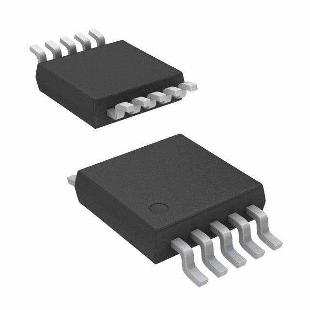
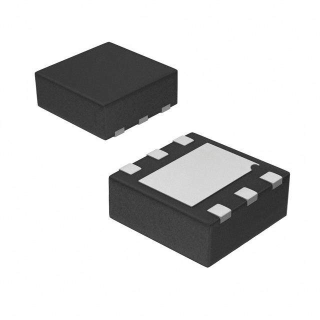
ICGOO电子元器件商城为您提供HMC603MS10E由Hittite设计生产,在icgoo商城现货销售,并且可以通过原厂、代理商等渠道进行代购。 HMC603MS10E价格参考。HittiteHMC603MS10E封装/规格:衰减器, RF Attenuator 0.5dB ~ 15.5dB 700MHz ~ 3.8GHz 50 Ohms 10-TFSOP,10-MSOP(0.118",3.00mm 宽)。您可以下载HMC603MS10E参考资料、Datasheet数据手册功能说明书,资料中有HMC603MS10E 详细功能的应用电路图电压和使用方法及教程。
| 参数 | 数值 |
| 产品目录 | |
| 描述 | IC ATTENUATOR 0.4-2.5GHZ 10-MSOP |
| 产品分类 | |
| 品牌 | Hittite Microwave Corporation |
| 数据手册 | |
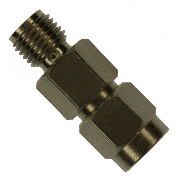
| 产品图片 |
|
| 产品型号 | HMC603MS10E |
| rohs | 无铅 / 符合限制有害物质指令(RoHS)规范要求 |
| 产品系列 | - |
| 其它名称 | 1127-1477 |
| 功率(W) | - |
| 容差 | - |
| 封装/外壳 | 10-TFSOP,10-MSOP(0.118",3.00mm 宽) |
| 标准包装 | 1 |
| 衰减值 | 0.5dB ~ 15.5dB |
| 配用 | /product-detail/zh/112747-HMC603MS10E/112747-HMC603MS10E-ND/3973357 |
| 阻抗 | 50 欧姆 |
| 频率范围 | 700MHz ~ 3.8GHz |


- 商务部:美国ITC正式对集成电路等产品启动337调查
- 曝三星4nm工艺存在良率问题 高通将骁龙8 Gen1或转产台积电
- 太阳诱电将投资9.5亿元在常州建新厂生产MLCC 预计2023年完工
- 英特尔发布欧洲新工厂建设计划 深化IDM 2.0 战略
- 台积电先进制程称霸业界 有大客户加持明年业绩稳了
- 达到5530亿美元!SIA预计今年全球半导体销售额将创下新高
- 英特尔拟将自动驾驶子公司Mobileye上市 估值或超500亿美元
- 三星加码芯片和SET,合并消费电子和移动部门,撤换高东真等 CEO
- 三星电子宣布重大人事变动 还合并消费电子和移动部门
- 海关总署:前11个月进口集成电路产品价值2.52万亿元 增长14.8%


PDF Datasheet 数据手册内容提取
HMC603MS10 603MS10E / v00.0905 0.5 dB LSB GaAs MMIC 5-BIT DIGITAL POSITIVE CONTROL ATTENUATOR, 0.7 - 3.8 GHz 5 Typical Applications Features The HMC603MS10 / HMC603MS10E is ideal for: 0.5 dB LSB Steps to 15.5 dB T M (cid:129) Cellular/3G Infrastructure Single Positive Control Per Bit S (cid:129) ISM, MMDS ± 0.15 dB Typical Bit Error - (cid:129) WLAN, WiMAX, & WiBro High Input IP3: +50 dBm S MSOP10 SMT Package R O T Functional Diagram General Description A U The HMC603MS10 & HMC603MS10E are general N purpose broadband 5-bit positive control GaAs IC E digital attenuators in 10 lead MSOP surface mount T plastic packages. Covering 0.7 to 3.8 GHz, the inser- T tion loss is less than 2.0 dB typical. The attenuator A bit values are 0.5 (LSB), 1, 2, 4 and 8 dB for a total attenuation of 15.5 dB. Attenuation accuracy is excellent at ± 0.15 dB typical with an IIP3 of +50 dBm. Five bit control voltage inputs, toggled between 0 and +3 to +5V, are used to select each attenuation state at less than 1.0 uA each. A single Vdd bias of +3 to +5V applied through an external 5K Ohm resistor is required. Electrical Specifi cations, T = +25° C, Vdd= +3V to +5V & Vctl= 0/Vdd (Unless Otherwise Stated) A Parameter Frequency (GHz) Min. Typical Max. Units 0.7 - 1.4 1.3 1.6 dB 1.4 - 2.3 1.7 2.0 dB Insertion Loss 2.3 - 2.7 2.2 2.5 dB 2.7 - 3.8 2.7 3.1 dB Attenuation Range 15.5 dB 0.7 - 1.4 25 dB 1.4 - 2.3 18 dB Return Loss (RF1 & RF2, All Atten. States) 2.3 - 2.7 13 dB 2.7 - 3.8 12 dB Attenuation Accuracy: (Referenced to Insertion Loss) dB 0.7 - 2.2 ± (0.2 + 2% of Atten. Setting) Max. All States dB 2.2 - 3.8 ± (0.3 + 3% of Atten. Setting) Max. Vdd = 5V 29 dBm Input Power for 0.1 dB Compression 0.7 - 3.8 Vdd = 3V 28 dBm Input Third Order Intercept Point REF - 2 dB States 53 dBm 0.7 - 3.8 (Two-tone Input Power = 0 dBm Each Tone) 2.5 - 15.5 dB States 48 dBm Switching Characteristics 0.7 - 3.8 1.6 µs tRISE, tFALL (10/90% RF) 1.6 µs tON, tOFF (50% CTL to 10/90% RF) Information furnisheFd obyr Apnrailocge D,e dviceesl ivis ebreylie,v eadn tod bteo a cpcularacte ea nod rrdelieabrlse., Hpowleevaers, eno coFnotra pcritc He, idtteitlieve Mry, icanrdo wtoa pvleac Ce oorrdpeorsr: aAtnioanlo:g Devices, Inc., 5 - 190 rriegshptso nosf ibthiilritdy pisa artsiessu mthea2dt m0bya yAA rnelaspluolhgt faDroe mvRi citeos sua fsoedr. i,tSs p Cuescheif,i ecnaoltrmio fnossr asfnuoyb rjiendcfrt,i nt ogM ecmhAaenn gt0se 1owf8 iptha2otue4tn tnsPo otihcr eoo.t hNneore : 9OPh7noe8n T-ee2: c57h80n1o--33lo23g9y4- 4W37 a0 y0F, a(cid:127)P .xOO:r. d 9Be7or x8o n9-l12in05e6 0,a N-t 3wor3ww7wo3o.adn, aMloAg .0c2o0m6 2-9106 lTicraednesem aisr kgsr aanndte dre gbiys teimrepdli ctraatdioenm oarr kost haerrew tihsee purnodpeerr tya noyf tphaetier nret sOopre prcadtivteeen otr w riOgnehrtnss .-olf iAnneal oag tD ewvicwesw. .hAiptptilticea.tcioonm Support: Phone: 1-800-ANALOG-D
HMC603MS10 / 603MS10E v00.0905 0.5 dB LSB GaAs MMIC 5-BIT DIGITAL POSITIVE CONTROL ATTENUATOR, 0.7 - 3.8 GHz 5 Return Loss RF1, RF2 Insertion Loss (Only Major States are Shown) 0 0 T -0.5 -5 M SS (dB)-1-.51 S (dB) -10 I.L 1 dB 8 dB S O S - ON L -2 N LO -15 0.5 dB S INSERTI-2-.53 +25 C RETUR -20 2 dB OR +85 C -25 T -3.5 -40 C 4 dB A 15.5 dB -4 -30 U 0.5 1 1.5 2 2.5 3 3.5 4 0.5 1 1.5 2 2.5 3 3.5 4 N FREQUENCY (GHz) FREQUENCY (GHz) E T Normalized Attenuation T (Only Major States are Shown) Bit Error vs. Attenuation State A 0 0.5 B) d UATION ( --63 dB) 0.3 3.5 GHz 2.4 GHz EN R ( T O T -9 R 0.1 D A ER LIZE -12 BIT MA -0.1 OR -15 N 0.9 GHz 1.9 GHz -18 -0.3 0.5 1 1.5 2 2.5 3 3.5 4 0.5 3.5 6.5 9.5 12.5 15.5 FREQUENCY (GHz) ATTENUATION STATE (dB) Bit Error vs. Frequency Relative Phase vs. Frequency (Only Major States are Shown) (Only Major States are Shown) 0.6 40 1 dB 0.5 dB 0.3 eg) 20 dB) E (d 15.5 dB R ( AS 8 dB 4 dB O H R 0 P 0 R E E V T TI BI A L -0.3 2 dB RE -20 0.5, 1, 2 dB 15.5 dB 4 dB 8 dB -0.6 -40 0.5 1 1.5 2 2.5 3 3.5 4 0.5 1 1.5 2 2.5 3 3.5 4 FREQUENCY (GHz) FREQUENCY (GHz) Information furnisheFd obyr Apnrailocge D,e dviceesl ivis ebreylie,v eadn tod bteo a cpcularacte ea nod rrdelieabrlse., Hpowleevaers, eno coFnotra pcritc He, idtteitlieve Mry, icanrdo wtoa pvleac Ce oorrdpeorsr: aAtnioanlo:g Devices, Inc., responsibility is assume2d 0by AAnlaplohg aDe vRiceosa fodr i,ts Cushe, enolrm fosr afnoy rindfr,in gMemAen t0s 1of8 pa2te4n tsP ohr oothnere : 9O7ne8 T-e2c5h0no-3lo3gy4 W3 a yF, aP.xO:. 9B7ox8 9-120560, N-3or3w7o3od, MA 02062-9106 5 - 191 rights of third parties that may result from its use. Specifications subject to change without notice. No Phone: 781-329-4700 (cid:127) Order online at www.analog.com lTicraednesem aisr kgsr aanndte dre gbiys teimrepdli ctraatdioenm oarr kost haerrew tihsee purnodpeerr tya noyf tphaetier nret sOopre prcadtivteeen otr w riOgnehrtnss .-olf iAnneal oag tD ewvicwesw. .hAiptptilticea.tcioonm Support: Phone: 1-800-ANALOG-D
HMC603MS10 / 603MS10E v00.0905 0.5 dB LSB GaAs MMIC 5-BIT DIGITAL POSITIVE CONTROL ATTENUATOR, 0.7 - 3.8 GHz 5 Worst Case Step Error Truth Table T 00..56 Control Voltage Input Attenuation M 0.4 8V d1B 4V d2B 2V d3B 1V d4B 0.5V 5dB RFS1t a- tReF2 0.3 S dB) 0.2 High High High High High Reference I.L. - OR ( 0.1 High High High High Low 0.5 dB S ERR 0 High High High Low High 1 dB R P -0.1 TE-0.2 High High Low High High 2 dB O S -0.3 High Low High High High 4 dB T -0.4 Low High High High High 8 dB A -0.5 U -0.6 Low Low Low Low Low 15.5 dB 0.5 1 1.5 2 2.5 3 3.5 4 Max. Atten. N FREQUENCY (GHz) Any combination of the above states will provide an attenuation E approximately equal to the sum of the bits selected. T T A Bias Voltage & Current Control & Bias Voltages Vdd = +5.0 Vdc ± 10% State Bias Condition Vdd Idd (Typ.) Low 0 to +0.2V @ 1.0 µA Max. (VDC) (µA) High Vdd ± 0.2V @ 0.5 µA Max. +3.0 4.0 Note: Vdd = +3V to +5V ± 0.2V +5.0 5.0 0.00.20.2 Application Circuit Note: DC Blocking Capacitors C1 & C2 are required on RF1 & RF2. Choose C1 = C2 = 100 ~ 300 pF to allow lowest customer specifi c frequency to pass with minimal loss. R1= 5K Ohm is required to supply voltage to the circuit through either Pin 6 or Pin 10. Information furnisheFd obyr Apnrailocge D,e dviceesl ivis ebreylie,v eadn tod bteo a cpcularacte ea nod rrdelieabrlse., Hpowleevaers, eno coFnotra pcritc He, idtteitlieve Mry, icanrdo wtoa pvleac Ce oorrdpeorsr: aAtnioanlo:g Devices, Inc., 5 - 192 rriegshptso nosf ibthiilritdy pisa artsiessu mthea2dt m0bya yAA rnelaspluolhgt faDroe mvRi citeos sua fsoedr. i,tSs p Cuescheif,i ecnaoltrmio fnossr asfnuoyb rjiendcfrt,i nt ogM ecmhAaenn gt0se 1owf8 iptha2otue4tn tnsPo otihcr eoo.t hNneore : 9OPh7noe8n T-ee2: c57h80n1o--33lo23g9y4- 4W37 a0 y0F, a(cid:127)P .xOO:r. d 9Be7or x8o n9-l12in05e6 0,a N-t 3wor3ww7wo3o.adn, aMloAg .0c2o0m6 2-9106 lTicraednesem aisr kgsr aanndte dre gbiys teimrepdli ctraatdioenm oarr kost haerrew tihsee purnodpeerr tya noyf tphaetier nret sOopre prcadtivteeen otr w riOgnehrtnss .-olf iAnneal oag tD ewvicwesw. .hAiptptilticea.tcioonm Support: Phone: 1-800-ANALOG-D
HMC603MS10 / 603MS10E v00.0905 0.5 dB LSB GaAs MMIC 5-BIT DIGITAL POSITIVE CONTROL ATTENUATOR, 0.7 - 3.8 GHz 5 Absolute Maximum Ratings RF Input Power (0.7 - 3.8 GHz) +30 dBm ELECTROSTATIC SENSITIVE DEVICE T Control Voltage (V1 - V5) Vdd + 0.5 Vdc M OBSERVE HANDLING PRECAUTIONS Bias Voltage (Vdd) +8.0 Vdc S Channel Temperature 150 °C - Thermal Resistance 182 °C/W S Storage Temperature -65 to +150 °C R Operating Temperature -40 to +85 °C O ESD Sensitivity (HBM) Class 1A T A Outline Drawing U N E T T A NOTES: 1. LEADFRAME MATERIAL: COPPER ALLOY 2. DIMENSIONS ARE IN INCHES [MILLIMETERS]. 3. DIMENSION DOES NOT INCLUDE MOLDFLASH OF 0.15mm PER SIDE. 4. DIMENSION DOES NOT INCLUDE MOLDFLASH OF 0.25mm PER SIDE. 5. ALL GROUND LEADS MUST BE SOLDERED TO PCB RF GROUND. Package Information Part Number Package Body Material Lead Finish MSL Rating Package Marking [3] HMC603MS10 Low Stress Injection Molded Plastic Sn/Pb Solder MSL1 [1] H603 XXXX HMC603MS10E RoHS-compliant Low Stress Injection Molded Plastic 100% matte Sn MSL1 [2] H603 XXXX [1] Max peak refl ow temperature of 235 °C [2] Max peak refl ow temperature of 260 °C [3] 4-Digit lot number XXXX Information furnisheFd obyr Apnrailocge D,e dviceesl ivis ebreylie,v eadn tod bteo a cpcularacte ea nod rrdelieabrlse., Hpowleevaers, eno coFnotra pcritc He, idtteitlieve Mry, icanrdo wtoa pvleac Ce oorrdpeorsr: aAtnioanlo:g Devices, Inc., responsibility is assume2d 0by AAnlaplohg aDe vRiceosa fodr i,ts Cushe, enolrm fosr afnoy rindfr,in gMemAen t0s 1of8 pa2te4n tsP ohr oothnere : 9O7ne8 T-e2c5h0no-3lo3gy4 W3 a yF, aP.xO:. 9B7ox8 9-120560, N-3or3w7o3od, MA 02062-9106 5 - 193 rights of third parties that may result from its use. Specifications subject to change without notice. No Phone: 781-329-4700 (cid:127) Order online at www.analog.com lTicraednesem aisr kgsr aanndte dre gbiys teimrepdli ctraatdioenm oarr kost haerrew tihsee purnodpeerr tya noyf tphaetier nret sOopre prcadtivteeen otr w riOgnehrtnss .-olf iAnneal oag tD ewvicwesw. .hAiptptilticea.tcioonm Support: Phone: 1-800-ANALOG-D
HMC603MS10 / 603MS10E v00.0905 0.5 dB LSB GaAs MMIC 5-BIT DIGITAL POSITIVE CONTROL ATTENUATOR, 0.7 - 3.8 GHz 5 Pin Descriptions Pin Number Function Description Interface Schematic T M 1 - 5 V1 - V5 See truth table and control voltage table. S - This pin is DC coupled and matched to 50 Ohm. S 6 RF2 A blocking capacitor is required. R O T 7 - 9 GND These pins must be DC grounded. A U N 10 RF1 This pin is DC coupled and matched to 50 Ohm. A blocking capacitor is required. E T T A Information furnisheFd obyr Apnrailocge D,e dviceesl ivis ebreylie,v eadn tod bteo a cpcularacte ea nod rrdelieabrlse., Hpowleevaers, eno coFnotra pcritc He, idtteitlieve Mry, icanrdo wtoa pvleac Ce oorrdpeorsr: aAtnioanlo:g Devices, Inc., 5 - 194 rriegshptso nosf ibthiilritdy pisa artsiessu mthea2dt m0bya yAA rnelaspluolhgt faDroe mvRi citeos sua fsoedr. i,tSs p Cuescheif,i ecnaoltrmio fnossr asfnuoyb rjiendcfrt,i nt ogM ecmhAaenn gt0se 1owf8 iptha2otue4tn tnsPo otihcr eoo.t hNneore : 9OPh7noe8n T-ee2: c57h80n1o--33lo23g9y4- 4W37 a0 y0F, a(cid:127)P .xOO:r. d 9Be7or x8o n9-l12in05e6 0,a N-t 3wor3ww7wo3o.adn, aMloAg .0c2o0m6 2-9106 lTicraednesem aisr kgsr aanndte dre gbiys teimrepdli ctraatdioenm oarr kost haerrew tihsee purnodpeerr tya noyf tphaetier nret sOopre prcadtivteeen otr w riOgnehrtnss .-olf iAnneal oag tD ewvicwesw. .hAiptptilticea.tcioonm Support: Phone: 1-800-ANALOG-D
HMC603MS10 / 603MS10E v00.0905 0.5 dB LSB GaAs MMIC 5-BIT DIGITAL POSITIVE CONTROL ATTENUATOR, 0.7 - 3.8 GHz 5 Evaluation Circuit Board T M S - S R O T A U N E T T A * R2 - R6= 100 Ohm. These resistors are optional and may be used to enhance decoupling of the RF path from the control inputs. List of Materials for Evaluation PCB 112747 [1] The circuit board used in the fi nal application should Item Description use RF circuit design techniques. Signal lines should J1 - J2 PCB Mount SMA Connector have 50 ohm impedance while the package ground J3 - J8 DC Pin leads should be connected directly to the ground R1 5k Ohm Resistor, 0402 Pkg. plane similar to that shown. A sufficient number of R2 - R6 100 Ohm Resistor, 0402 Pkg. via holes should be used to connect the top and 0402 Chip Capacitor, Select Value for Lowest C1 - C2 Frequency bottom ground planes. The evaluation circuit board HMC603MS10 / HMC603MS10E shown is available from Hittite upon request. U1 Digital Attenuators PCB [2] 112746 Evaluation PCB [1] Reference this number when ordering complete evaluation PCB [2] Circuit Board Material: Rogers 4350 Information furnisheFd obyr Apnrailocge D,e dviceesl ivis ebreylie,v eadn tod bteo a cpcularacte ea nod rrdelieabrlse., Hpowleevaers, eno coFnotra pcritc He, idtteitlieve Mry, icanrdo wtoa pvleac Ce oorrdpeorsr: aAtnioanlo:g Devices, Inc., responsibility is assume2d 0by AAnlaplohg aDe vRiceosa fodr i,ts Cushe, enolrm fosr afnoy rindfr,in gMemAen t0s 1of8 pa2te4n tsP ohr oothnere : 9O7ne8 T-e2c5h0no-3lo3gy4 W3 a yF, aP.xO:. 9B7ox8 9-120560, N-3or3w7o3od, MA 02062-9106 5 - 195 rights of third parties that may result from its use. Specifications subject to change without notice. No Phone: 781-329-4700 (cid:127) Order online at www.analog.com lTicraednesem aisr kgsr aanndte dre gbiys teimrepdli ctraatdioenm oarr kost haerrew tihsee purnodpeerr tya noyf tphaetier nret sOopre prcadtivteeen otr w riOgnehrtnss .-olf iAnneal oag tD ewvicwesw. .hAiptptilticea.tcioonm Support: Phone: 1-800-ANALOG-D