 Datasheet下载
- 型号: GQM22M5C2H9R0CB01L
- 制造商: Murata
- 库位|库存: xxxx|xxxx
- 要求:
| 数量阶梯 | 香港交货 | 国内含税 |
| +xxxx | $xxxx | ¥xxxx |
查看当月历史价格
查看今年历史价格
GQM22M5C2H9R0CB01L产品简介:
ICGOO电子元器件商城为您提供GQM22M5C2H9R0CB01L由Murata设计生产,在icgoo商城现货销售,并且可以通过原厂、代理商等渠道进行代购。 GQM22M5C2H9R0CB01L价格参考。MurataGQM22M5C2H9R0CB01L封装/规格:陶瓷电容器, 9pF ±0.25pF 500V 陶瓷电容器 C0G,NP0 1111(2828 公制)。您可以下载GQM22M5C2H9R0CB01L参考资料、Datasheet数据手册功能说明书,资料中有GQM22M5C2H9R0CB01L 详细功能的应用电路图电压和使用方法及教程。
| 参数 | 数值 |
| 产品目录 | |
| 描述 | CAP CER 9PF 500V NP0 1111多层陶瓷电容器MLCC - SMD/SMT 1111 C0G 500V 9.0pF |
| 产品分类 | |
| 品牌 | Murata Electronics |
| 产品手册 | |
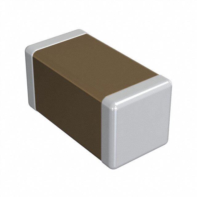
| 产品图片 |
|
| rohs | 符合RoHS无铅 / 符合限制有害物质指令(RoHS)规范要求 |
| 产品系列 | MLCC,多层陶瓷电容器MLCC - SMD/SMT,Murata Electronics GQM22M5C2H9R0CB01LGQM |
| 数据手册 | |
| 产品型号 | GQM22M5C2H9R0CB01L |
| 产品 | High Q MLCCs |
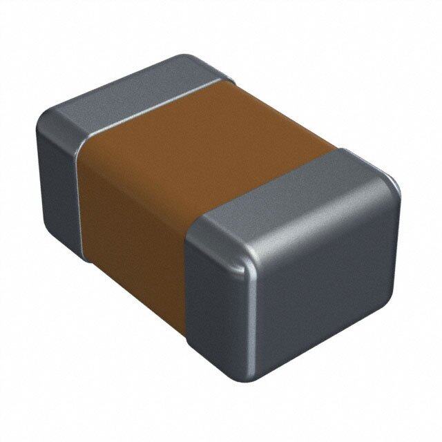
| 产品目录绘图 |
|
| 产品目录页面 | |
| 产品种类 | 多层陶瓷电容器MLCC - SMD/SMT |
| 其它名称 | 490-5507-6 |
| 包装 | Digi-Reel® |
| 厚度(最大值) | 0.053"(1.35mm) |
| 商标 | Murata Electronics |
| 外壳代码-in | 1111 |
| 外壳代码-mm | 2828 |
| 外壳宽度 | 2.8 mm |
| 外壳长度 | 2.8 mm |
| 外壳高度 | 1.15 mm |
| 大小/尺寸 | 0.110" 长x 0.110" 宽(2.80mm x 2.80mm) |
| 安装类型 | 表面贴装,MLCC |
| 容差 | 0.25 pF |
| 封装 | Reel |
| 封装/外壳 | 1111(2828 公制) |
| 封装/箱体 | 1111 (2828 metric) |
| 工作温度 | -55°C ~ 125°C |
| 工作温度范围 | - 55 C to + 125 C |
| 工厂包装数量 | 1000 |
| 应用 | RF,微波,高频 |
| 引线形式 | - |
| 引线间距 | - |
| 最大工作温度 | + 125 C |
| 最小工作温度 | - 55 C |
| 标准包装 | 1 |
| 温度系数 | C0G,NP0 |
| 温度系数/代码 | +/- 30 PPM / C |
| 特性 | 高 Q 值,低损耗 |
| 特色产品 | http://www.digikey.com/cn/zh/ph/Murata/Caps.html |
| 电介质 | C0G (NP0) |
| 电压-额定 | 500V |
| 电压额定值 | 500 V |
| 电压额定值DC | 500 V |
| 电容 | 9 pF |
| 端接类型 | SMD/SMT |
| 等级 | - |
| 类型 | High Frequency High Q Type |
| 系列 | GQM |
| 高度-安装(最大值) | - |

.jpg)


- 商务部:美国ITC正式对集成电路等产品启动337调查
- 曝三星4nm工艺存在良率问题 高通将骁龙8 Gen1或转产台积电
- 太阳诱电将投资9.5亿元在常州建新厂生产MLCC 预计2023年完工
- 英特尔发布欧洲新工厂建设计划 深化IDM 2.0 战略
- 台积电先进制程称霸业界 有大客户加持明年业绩稳了
- 达到5530亿美元!SIA预计今年全球半导体销售额将创下新高
- 英特尔拟将自动驾驶子公司Mobileye上市 估值或超500亿美元
- 三星加码芯片和SET,合并消费电子和移动部门,撤换高东真等 CEO
- 三星电子宣布重大人事变动 还合并消费电子和移动部门
- 海关总署:前11个月进口集成电路产品价值2.52万亿元 增长14.8%


PDF Datasheet 数据手册内容提取
C02E.pdf Nov.27,2017 Chip Multilayer Ceramic Capacitors for General 2018
!Note (cid:129) Please read rating and !CAUTION (for storage, operating, rating, soldering, mounting and handling) in this catalog to prevent smoking and/or burning, etc. C02E.pdf (cid:129) This catalog has only typical specifications. Therefore, please approve our product specifications or transact the approval sheet for product specifications before ordering. Nov.27,2017 Contents Product specifications are as of September 2017. Explanation of Symbols in This Catalog p2 Part Numbering p5 Selection Guide p3 Capacitance Table p9 Catalog information p4 Cap. Table Chip Multilayer Ceramic Capacitors for General Purpose GRM Series p40 p10 GRM Series Specifications and Test Methods p108 High Effective Capacitance & High Ripple Current Chip Multilayer Ceramic Capacitors for General Purpose GR3 Series p109 p27 GR3 Series Specifications and Test Methods (1) p111 GR3 Series Specifications and Test Methods (2) p114 GR3 Series Specifications and Test Methods (3) p117 Soft Termination Chip Multilayer Ceramic Capacitors for General Purpose GRJ Series p120 p28 GRJ Series Specifications and Test Methods p124 Chip Multilayer Ceramic Capacitors for Ethernet LAN and Primary-secondary Coupling of DC-DC Converters GR4 Series p125 p30 GR4 Series Specifications and Test Methods (1) p127 Chip Multilayer Ceramic Capacitors for Camera Flash circuit only GR7 Series p130 p30 GR7 Series Specifications and Test Methods (1) p132 High Q Chip Multilayer Ceramic Capacitors for General Purpose GJM Series p135 p30 GJM Series Specifications and Test Methods (1) p157 GJM Series Specifications and Test Methods (2) p160 High Q and High Power Chip Multilayer Ceramic Capacitors for General Purpose GQM Series p164 p31 GQM Series Specifications and Test Methods (1) p172 GQM Series Specifications and Test Methods (2) p175 GQM Series Specifications and Test Methods (3) p178 GQM Series Specifications and Test Methods (4) p181 Based on the Electrical Appliance and Material Safety Law of Japan Chip Multilayer Ceramic Capacitors for General Purpose GA2 Series p184 p32 GA2 Series Specifications and Test Methods (1) p186 Safety Standard Certified Chip Multilayer Ceramic Capacitors for General Purpose / IEC60384-14 Class X2 GA3 Series Type GB p189 p32 GA3 Series Type GB Specifications and Test Methods (1) p192 Safety Standard Certified Chip Multilayer Ceramic Capacitors for General Purpose / Acquired certifications of UL60950-1 GA3 Series Type GD p196 p32 GA3 Series Type GD Specifications and Test Methods (1) p199 GA3 Series Type GD Specifications and Test Methods (2) p203 Safety Standard Certified Chip Multilayer Ceramic Capacitors for General Purpose / Acquired certifications of IEC60384-14 Class X1/Y2 and UL60950-1 GA3 Series Type GF p207 p33 GA3 Series Type GF Specifications and Test Methods (1) p211 GA3 Series Type GF Specifications and Test Methods (2) p215 LW Reversed Low ESL Chip Multilayer Ceramic Capacitors for General Purpose LLL Series p219 p34 LLL Series Specifications and Test Methods p221
!Note (cid:129) Please read rating and !CAUTION (for storage, operating, rating, soldering, mounting and handling) in this catalog to prevent smoking and/or burning, etc. C02E.pdf (cid:129) This catalog has only typical specifications. Therefore, please approve our product specifications or transact the approval sheet for product specifications before ordering. Nov.27,2017 M R G 3 R G J R G Cap. Table 8 Terminals Low ESL Chip Multilayer Ceramic Capacitors for General Purpose 4 LLA Series p222 p34 R G LLA Series Specifications and Test Methods (1) p224 LLA Series Specifications and Test Methods (2) p226 7 R 10 Terminals Low ESL Chip Multilayer Ceramic Capacitors for General Purpose G LLM Series p228 p35 LLM Series Specifications and Test Methods (1) p230 M J G LW Reversed Controlled ESR Low ESL Chip Multilayer Ceramic Capacitors for General Purpose LLR Series p232 p35 M LLR Series Specifications and Test Methods (1) p234 Q G 3 Terminals Low ESL Chip Multilayer Ceramic Capacitors for General Purpose NFM Series p236 p35 2 A NFM Series Specifications and Test Methods p238 G M eKtRaMl T Seermrieinsa l Type Multilayer Ceramic Capacitors for General Purpose p239 p36 A3GB G KRM Series Specifications and Test Methods p242 High Effective Capacitance & High Allowable Ripple Current Metal Terminal Type A3GD Multilayer Ceramic Capacitors for General Purpose KR3 Series p243 p37 G KR3 Series Specifications and Test Methods (1) p246 Wire Bonding Mount Multilayer Microchip Capacitors for General Purpose GA3GF GMA Series p249 p37 GMA Series Specifications and Test Methods (1) p252 L GMA Series Specifications and Test Methods (2) p254 LL Wire Bonding/AuSn Soldering Mount Chip Multilayer Ceramic Capacitors for General Purpose GMD Series p256 p38 A L L GMD Series Specifications and Test Methods (1) p259 GMD Series Specifications and Test Methods (2) p261 M GMD Series Specifications and Test Methods (3) p263 L L !Caution/Notice/Soldering and Mounting p265 Introduction of Website SimSurfing p291 R L L Product Information p292 Please check the MURATA website (https://www.murata.com/) M if you cannot find a part number in this catalog. F N M R K EU RoHS Compliant 3 R K (cid:70)(cid:3)All the products in this catalog comply with EU RoHS. (cid:70)(cid:3)EU RoHS is "the European Directive 2011/65/EU on the Restriction of the Use of Certain Hazardous Substances in Electrical and Electronic Equipment." A (cid:70)(cid:3)For more details, please refer to our web page, "Murata's Approach for EU RoHS" (https://www.murata.com/en- M G eu/support/compliance/rohs). Qualified Standards MD G (cid:70)(cid:3)The products listed here have been produced by ISO 9001 certified factory. <Plant> (cid:3)(cid:3)(cid:3)(cid:3)(cid:3)(cid:3)(cid:3)(cid:3)(cid:3)(cid:3)(cid:3)(cid:3)(cid:70)(cid:70)(cid:70)(cid:3)(cid:3)(cid:3)FIMzuuukmruaiot Ma M uEurleraacttatar Mo Mnfigfcg.s .C CSoio.n,. ,gL Lattdpd.o.re (Pte.) Ltd. Caution!/Notice (cid:3)(cid:3)(cid:3)(cid:3)(cid:70)(cid:3)Wuxi Murata Electronics Co., Ltd. (cid:3)(cid:3)(cid:3)(cid:3)(cid:70)(cid:3)PHILIPPINE MANUFACTURING CO. OF MURATA, INC. 1
!Note (cid:129) Please read rating and !CAUTION (for storage, operating, rating, soldering, mounting and handling) in this catalog to prevent smoking and/or burning, etc. C02E.pdf (cid:129) This catalog has only typical specifications. Therefore, please approve our product specifications or transact the approval sheet for product specifications before ordering. Nov.27,2017 Explanation of Symbols in This Catalog WEB Links are provided to the latest information from the PDF version of the catalog, which is available on the web. For applications that do not require the particular reliability such as Derating 1 the general equipment This product is suitable when a voltage continuously applied to a capacitor in an operating circuit, is used below (derated) the rated voltage of the capacitor. This model guarantees the test conditions in Infotainment for Automotive the endurance test, at a rated voltage x 100% at the maximum The product for entertainment equipment like car navigations, car operating temperature. A reliability assurance level equivalent to a audios, and body control equipment like wipers, power windows. common product can be secured, by using this product within the voltage and temperature derated conditions recommended in the Powertrain/Safety for Automotive figure below. Product used for applications (running, turning, stopping and safety devices) which particularly concern human life, such as in devices for Recommended Conditions of the Derating Operating Voltage and Temperature automobiles. %)120 MTheedsieca pl-rogdraudcet sp arored uincttesn fdoer dIm foprl aunstee idn Mimepdliacnatl eDde mviceedsical devices Voltage (100 125°C Type sgT*u1ah cseNhtyor iaancsr- e eccl raesiturciditctriaaaolbcs c ltpeiirma cfcouuerilt maustsaoekr sein.r sn,o cno-cchrlietiacra ilm ciprclaunittss., *i1nsulin pumps and Voltage/Rated 486000 18055°C°C T yTpyepe Tnenohdtis ad tniergeremcrt ltryhe lfeien lrkisfee td oo t fc oti rhlciefue pi tsasut ipinep niomtr stp,hl aio.enu.t lcedid rtc hmueie tfdsu intchcaatl itdo wenvailillci tneyos o tt fhd tairhtee ca trely Operating 200 device be reduced or halted by failure of the circuit. 0 25 50 75 100 125 150 Product Temperature (°C) AEC-Q200 compliant product Derating 2 When the product temperature exceeds 105°C, please use this product within the voltage and temperature derated conditions in the Safety Standard Certified Product figure below. Products that acquired safety standard certification IEC60384-14 and products based on the Electrical Appliance and Material Safety 700 Law of Japan. Rated Voltage 630V %) 600 LBdBPsaoiryasofw sseddei tepuddyvaci soilttsasinsoiwin p nttga hh o itacsefi et o aJE rnacalae rhpfmecoiae tribncrv hai. ecmsidagea lhid nAt f e orpfrernpieaq ltqiluahsue neaenc nencedlcye a yecn ltbedraic cMntadralos tad eoperfp i maVlilaH aSntFace,f erUei ataHylnsF d,L ala omnwwda otef rJiaalp an oltage/Rated Voltage ( ((434355500000000VV)) Rated Voltage 450V microwave or beyond. ng V 200 LTohwis cinadpuacctiatonrc ies designed so that the parasitic inductance Operati 100 component (ESL) that the capacitor has on the high frequency side becomes lower. 0 0 25 50 75 100 125 150 Fail safe product Product Temperature (°C) This capacitor is designed to prevent failures as much as possible by Derating 3 short mode. Please apply the derating curve according to the operating temperature. Product resistant to deflection cracking Please refer to detailed specifications sheet for details. This capacitor is designed to prevent failures as much as possible by short mode caused by cracking when there is board deflection. Derating 4 When the product temperature exceeds 125°C, please use this Product with solder cracking suppression product within the voltage and temperature derated conditions in the “This capacitor is configured with metal terminals and leads figure below. connected to the chip. The metal terminals and leads relieve the stress from expansion and contraction of the solder, to suppress %) 120 PTccsoeohrolrnidsadfi empugrrcu icoctrrd acsautuacicoipkttnaia ns.cbguilt.ep”o pfror iesr s auscseoesud as, ctboiycu dnseotivicsi esni onreigsd etuh, cwet ihmoinca htae nordciac lluosr wasn dwdish teonr taio n Voltage/Rated Voltage ( 1(0486500000) NPalooul myDmiCne ubrmi ac sao pcxahidcaiizrtaeocdr t ifies rlnmisot ficcoasrp daiecliteacntrciec .change with DC bias due to Operating 200-75 -50 -25 0 25 50 75 100 125 150 175 Product Temperature (°C) Low-inductance product suitable for noise suppression. This product has extremely low ESL and is suitable for suppression Derating 5 of noise, including high frequencies. Please apply the rated voltage derating over 150 °C. This product can also be used as a low-ESL, high-performance Please refer to detailed specifications sheet for details. bypass capacitor. Product for bonding Since gold is used for the external electrodes, the capacitor can be mounted by die bonding/wire bonding. 2
!Note (cid:129) Please read rating and !CAUTION (for storage, operating, rating, soldering, mounting and handling) in this catalog to prevent smoking and/or burning, etc. C02E.pdf (cid:129) This catalog has only typical specifications. Therefore, please approve our product specifications or transact the approval sheet for product specifications before ordering. Nov.27,2017 Selection Guide for Capacitors For general Infotainment for automotive SMD SMD Solder mounting Solder mounting Chip type Chip type GRM p40 GRT WEB GRM For LCD backlight inverter circuit WEB only GR3 High effective capacitance & p109 Powertrain/Safety for automotive high ripple current GRJ Soft termination p120 SMD GXM WEB Solder mounting GR4 For information devices only p125 Chip type GR7 For camera flash circuit only p130 GCM WEB GJM p135 GC3 High effective capacitance & WEB high ripple current GQM High power p164 GCJ Soft termination WEB GA2 Based on the Electrical Appliance p184 GGM WEB and Material Safety Law of Japan GA3 p189 GCQ WEB LLL LW reversed p219 GCD MLSC design WEB LLA 8 terminals p222 GCE Soft termination MLSC design WEB LLM 10 terminals p228 GGD MLSC design WEB LLR LW reversed controlled ESR p232 NFM 3 terminals WEB NFM 3 terminals p236 Metal terminal type GJ4 Low distortion WEB KCM WEB GJ8 Low acoustic noise WEB KC3 Hhiigghh reipffpelcet civuer rceanptacitance & WEB On interposer board KCA WEB ZRA WEB Limited to Conductive Glue Mounting ZRB WEB Chip type Metal terminal type GCB Ni plating + Pd plating termination WEB conductive glue mounting KRM p239 GCG AgPd termination conductive glue WEB mounting KR3 High effective capacitance & p243 Lead type high ripple current Resin molding SMD type Solder mounting DK1 WEB RCE WEB Wire bonding mounting RHE 150°C operation leaded WEB Chip type RHS 200°C operation leaded WEB GMA Microchip p249 DE6 WEB GMD p256 Lead type Medical-grade products for implanted medical devices Solder mounting SMD RDE WEB Solder mounting DEH High temperature low loss WEB Chip type DEA High temperature Class 1 WEB GCH WEB DEB Class 2 WEB DEC WEB DEF For LCD backlight inverter circuit WEB only DHR WEB DEJ Based on the Electrical Appliance WEB and Material Safety Law of Japan DE1 X1/Y1 Class certified product WEB DE2 X1/Y2 Class certified product WEB Screw termination mounting DHS WEB DHK High voltage AC rated WEB 3
!Note (cid:129) Please read rating and !CAUTION (for storage, operating, rating, soldering, mounting and handling) in this catalog to prevent smoking and/or burning, etc. C02E.pdf (cid:129) This catalog has only typical specifications. Therefore, please approve our product specifications or transact the approval sheet for product specifications before ordering. Nov.27,2017 Catalog Information Catalog relates to a multilayer ceramic capacitor is below. Chip Multilayer Ceramic Capacitors Chip Multilayer Ceramic Capacitors for General for Automotive Cat No. C02E-21 Cat No. C03E-9 Safety Certified Ceramic Capacitors/ Radial Lead Type High Voltage Ceramic Capacitors Monolithic Ceramic Capacitors Cat No. C85E-5 Cat No. C49E-23 4
!Note (cid:129) Please read rating and !CAUTION (for storage, operating, rating, soldering, mounting and handling) in this catalog to prevent smoking and/or burning, etc. C02E.pdf (cid:129) This catalog has only typical specifications. Therefore, please approve our product specifications or transact the approval sheet for product specifications before ordering. Nov.27,2017 o Part Numbering WEB Chip Multilayer Ceramic Capacitors for General (Part Number) GR M 18 8 B1 1H 102 K A01 D 1 2 3 4 5 6 7 8 9 : 1Product ID 2Series Product ID Code Series 2 Based on the Electrical Appliance and Material Safety Law of Japan Chip Multilayer Ceramic Capacitors for General Purpose GA 3 Safety Standard Certified Chip Multilayer Ceramic Capacitors for General Purpose GJ M High Q Chip Multilayer Ceramic Capacitors for General Purpose A Wire Bonding Mount Multilayer Microchip Capacitors for General Purpose GM D Wire Bonding/AuSn Soldering Mount Chip Multilayer Ceramic Capacitors for General Purpose GQ M High Q and High Power Chip Multilayer Ceramic Capacitors for General Purpose 3 High Effective Capacitance & High Ripple Current Chip Multilayer Ceramic Capacitors for General Purpose 4 Chip Multilayer Ceramic Capacitors for Camera Flash Circuit only GR 7 Chip Multilayer Ceramic Capacitors for Ethernet LAN and Primary-secondary Coupling of DC-DC Converters J Soft Termination Chip Multilayer Ceramic Capacitors for General Purpose M Chip Multilayer Ceramic Capacitors for General Purpose 3 High Effective Capacitance & High Allowable Ripple Current Metal Terminal Type Multilayer Ceramic Capacitors for General Purpose KR M Metal Terminal Type Multilayer Ceramic Capacitors for General Purpose A 8 Terminals Low ESL Chip Multilayer Ceramic Capacitors for General Purpose L LW Reversed Low ESL Chip Multilayer Ceramic Capacitors for General Purpose LL M 10 Terminals Low ESL Chip Multilayer Ceramic Capacitors for General Purpose R LW Reversed Controlled ESR Low ESL Chip Multilayer Ceramic Capacitors for General Purpose 3Chip Dimensions (LxW) Code Dimensions (LxW) EIA 02 0.4x0.2mm 01005 0D 0.38x0.38mm 015015 03 0.6x0.3mm 0201 05 0.5x0.5mm 0202 08 0.8x0.8mm 0303 1U 0.6x1.0mm 02404 15 1.0x0.5mm 0402 18 1.6x0.8mm 0603 21 2.0x1.25mm 0805 22 2.8x2.8mm 1111 31 3.2x1.6mm 1206 32 3.2x2.5mm 1210 42 4.5x2.0mm 1808 43 4.5x3.2mm 1812 52 5.7x2.8mm 2211 55 5.7x5.0mm 2220 Continued on the following page. 5
!Note (cid:129) Please read rating and !CAUTION (for storage, operating, rating, soldering, mounting and handling) in this catalog to prevent smoking and/or burning, etc. C02E.pdf (cid:129) This catalog has only typical specifications. Therefore, please approve our product specifications or transact the approval sheet for product specifications before ordering. Nov.27,2017 (Part Number) GR M 18 8 B1 1H 102 K A01 D 1 2 3 4 5 6 7 8 9 : Continued from the preceding page. 4Height Dimension (T) (Except KRp) 4Height Dimension (T) (KRp Only) Code Dimension (T) Code Dimension (T) 2 0.2mm E 1.8mm 3 0.3mm F 1.9mm 4 0.4mm K 2.7mm 5 0.5mm L 2.8mm 6 0.6mm Q 3.7mm 7 0.7mm T 4.8mm 8 0.8mm W 6.4mm 9 0.85mm A 1.0mm B 1.25mm C 1.6mm D 2.0mm E 2.5mm M 1.15mm Q 1.5mm X Depends on individual standards. 5Temperature Characteristics Temperature Temperature Characteristics Capacitance Change Each Temperature (%) Characteristic Codes Operating Code Public Reference Temperature Caopra Tcietmanpceer aCthuarenge TemRpaenrgaeture –55°C *6 –10°C STD Code Temperature Range Coefficient Max. Min. Max. Min. Max. Min. 1X SL JIS 20°C 20 to 85°C +350 to –1000ppm/°C –55 to 125°C - - - - - - 2C CH JIS 20°C 20 to 125°C 0±60ppm/°C –55 to 125°C 0.82 –0.45 0.49 –0.27 0.33 –0.18 3C CJ JIS 20°C 20 to 125°C 0±120ppm/°C –55 to 125°C 1.37 –0.9 0.82 –0.54 0.55 –0.36 3U UJ JIS 20°C 20 to 85°C –750±120ppm/°C –25 to 85°C - - 4.94 2.84 3.29 1.89 4C CK JIS 20°C 20 to 125°C 0±250ppm/°C –55 to 125°C 2.56 –1.88 1.54 –1.13 1.02 –0.75 5C C0G EIA 25°C 25 to 125°C 0±30ppm/°C –55 to 125°C 0.58 –0.24 0.4 –0.17 0.25 –0.11 5G X8G *2 25°C 25 to 150°C 0±30ppm/°C –55 to 150°C 0.58 –0.24 0.4 –0.17 0.25 –0.11 7U U2J EIA 25°C 25 to 125°C *3 –750±120ppm/°C –55 to 125°C 8.78 5.04 6.04 3.47 3.84 2.21 B1 B *1 JIS 20°C –25 to 85°C ±10% –25 to 85°C - - - - - - B3 B JIS 20°C –25 to 85°C ±10% –25 to 85°C - - - - - - C7 X7S EIA 25°C –55 to 125°C ±22% –55 to 125°C - - - - - - C8 X6S EIA 25°C –55 to 105°C ±22% –55 to 105°C - - - - - - D7 X7T EIA 25°C –55 to 125°C +22%, –33% –55 to 125°C - - - - - - D8 X6T EIA 25°C –55 to 105°C +22%, –33% –55 to 105°C - - - - - - E7 X7U EIA 25°C –55 to 125°C +22%, –56% –55 to 125°C - - - - - - R1 R *1 JIS 20°C –55 to 125°C ±15% –55 to 125°C - - - - - - R6 X5R EIA 25°C –55 to 85°C ±15% –55 to 85°C - - - - - - R7 X7R EIA 25°C –55 to 125°C ±15% –55 to 125°C - - - - - - ±10% *4 - - - - - - W0 X7T EIA 25°C –55 to 125°C –55 to 125°C +22%, –33% *5 - - - - - - *1 Capacitance change is specified with 50% rated voltage applied. *2 Murata Temperature Characteristic Code. *3 Rated Voltage 100Vdc max: 25 to 85°C *4 Apply DC350V bias. *5 No DC bias. *6 –25°C (Reference Temperature 20°C) / –30°C (Reference Temperature 25°C) Continued on the following page. 6
!Note (cid:129) Please read rating and !CAUTION (for storage, operating, rating, soldering, mounting and handling) in this catalog to prevent smoking and/or burning, etc. C02E.pdf (cid:129) This catalog has only typical specifications. Therefore, please approve our product specifications or transact the approval sheet for product specifications before ordering. Nov.27,2017 (Part Number) GR M 18 8 B1 1H 102 K A01 D 1 2 3 4 5 6 7 8 9 : Continued from the preceding page. 6Rated Voltage 8Capacitance Tolerance Code Rated Voltage Code Capacitance Tolerance 0E DC2.5V B ±0.1pF 0G DC4V C ±0.25pF 0J DC6.3V ±0.5pF (Less than 10pF) D 1A DC10V ±0.5% (10pF and over) 1C DC16V F ±1% 1E DC25V G ±2% 1H DC50V J ±5% 1J DC63V K ±10% 1K DC80V M ±20% 2A DC100V W ±0.05pF 2D DC200V 2E DC250V 9Individual Specification Code (Except LLR) 2W DC450V Expressed by three figures. 2H DC500V 2J DC630V 9ESR (LLR Only) 3A DC1kV Code ESR 3D DC2kV E01 100mΩ 3F DC3.15kV E03 220mΩ BB DC350V E05 470mΩ E2 AC250V E07 1000mΩ GB X2; AC250V (Safety Standard Certified Type GB) GD Y3; AC250V (Safety Standard Certified Type GD) :Packaging GF Y2, X1/Y2; AC250V (Safety Standard Certified Type GF) Code Packaging YA DC35V L ø180mm Embossed Taping D/E/W ø180mm Paper Taping 7Capacitance K ø330mm Embossed Taping Expressed by three-digit alphanumerics. The unit is picofarad (pF). J/F ø330mm Paper Taping The first and second figures are significant digits, and the third figure expresses the number of zeros which follow the two T Bulk Tray numbers. If there is a decimal point, it is expressed by the capital letter "R." In this case, all figures are significant digits. If any alphabet, other than "R", is included, this indicates the specific part number is a non-standard part. Ex.) Code Capacitance R50 0.50pF 1R0 1.0pF 100 10pF 103 10000pF Please contact us if you find any part number not provided in this table. 7
!Note (cid:129) Please read rating and !CAUTION (for storage, operating, rating, soldering, mounting and handling) in this catalog to prevent smoking and/or burning, etc. C02E.pdf (cid:129) This catalog has only typical specifications. Therefore, please approve our product specifications or transact the approval sheet for product specifications before ordering. Nov.27,2017 WEB 3 Terminal Low ESL Multilayer Ceramic Capacitors (Part Number) NF M 3D CC 102 R 1H 3 L 1 2 3 4 5 6 7 8 9 1Product ID 2Series 7Rated Voltage Product ID Series Code Rated Voltage 3 Terminals Low ESL 0E 2.5V NFM Chip Multilayer Ceramic Capacitors 0G 4V 0J 6.3V 3Dimensions (LxW) 1A 10V Code Dimensions (LxW) EIA 1C 16V 15 1.0x0.5mm 0402 1E 25V 18 1.6x0.8mm 0603 1H 50V 21 2.0x1.25mm 0805 2A 100V 3D 3.2x1.25mm 1205 31 3.2x1.6mm 1206 8Electrode 41 4.5x1.6mm 1806 Code Electrode 3 Sn Plating 4Features Code Features 9Packaging CC For Signal Lines Code Packaging PC For Large Current B Bulk For General High Insertion Loss Type L Embossed Taping (ø180mm Reel) PS for Large Current D Paper Taping (ø180mm Reel) KC For Very Large Current 5Capacitance Expressed by three figures. The unit is in pico-farad (pF). The first and second figures are significant digits, and the third figure expresses the number of zeros that follow the two figures. 6Characteristics Code Capacitance Temperature Characteristics B ±10%, ±12.5%, +10/-13% C ±22% D +22/-33% F +30/-80%, +30/-84% R ±15%, +15/-18% 8
!Note (cid:129) Please read rating and !CAUTION (for storage, operating, rating, soldering, mounting and handling) in this catalog to prevent smoking and/or burning, etc. C02E.pdf (cid:129) This catalog has only typical specifications. Therefore, please approve our product specifications or transact the approval sheet for product specifications before ordering. Nov.27,2017 Capacitance Table How to read the Capacitance Table L×W (mm) 0.4×0.2 0.6 T max. (mm) 0.22 0. The values can be narrowed down in the order of size, Rated Voltage (Vdc) 25 50 rated voltage, and temperature characteristics. Cap. / TC Code C0G CΔ C0G CK CJ 0.10pF 0.20pF p140 p143 p146 p146 Refers to the page of the part number list. 1.0pF p140 p143 p146 Check the part number list for the applicable product number. 2.0pF p140 p143 p146 3.0pF p140 p143 p146 Temperature Characteristics Table The Table is colored by temperature characteristic codes. EIA: C0G U2J X7R X7S X7T X7U X6S X6T X5R Refer to the following Table for the meaning of each code. JIS: CK CJ CH SL UJ R B Murata Temperature Characteristic: X8G Temperature Temperature Characteristics Capacitance Change Each Temperature (%) Characteristic Codes Operating Temperature Public Reference Temperature Capacitance Change Range –55°C *3 –10°C or Temperature STD Code Temperature Range Coefficient Max. Min. Max. Min. Max. Min. C0G EIA 25°C 25 to 125°C 0±30ppm/°C –55 to 125°C 0.58 –0.24 0.4 –0.17 0.25 –0.11 CK JIS 20°C 20 to 125°C 0±250ppm/°C –55 to 125°C 2.56 –1.88 1.54 –1.13 1.02 –0.75 CJ JIS 20°C 20 to 125°C 0±120ppm/°C –55 to 125°C 1.37 –0.9 0.82 –0.54 0.55 –0.36 CH JIS 20°C 20 to 125°C 0±60ppm/°C –55 to 125°C 0.82 –0.45 0.49 –0.27 0.33 –0.18 SL JIS 20°C 20 to 85°C +350 to –1000ppm/°C –55 to 125°C - - - - - - U2J EIA 25°C 25 to 125°C *2 –750±120ppm/°C –55 to 125°C 8.78 5.04 6.04 3.47 3.84 2.21 UJ JIS 20°C 20 to 85°C –750±120ppm/°C –25 to 85°C - - 4.94 2.84 3.29 1.89 X8G *1 25°C 25 to 150°C 0±30ppm/°C –55 to 150°C 0.58 –0.24 0.4 –0.17 0.25 –0.11 X7R EIA 25°C –55 to 125°C ±15% –55 to 125°C - - - - - - X7S EIA 25°C –55 to 125°C ±22% –55 to 125°C - - - - - - X7T EIA 25°C –55 to 125°C +22%, –33% –55 to 125°C - - - - - - X7U EIA 25°C –55 to 125°C +22%, –56% –55 to 125°C - - - - - - R JIS 20°C –55 to 125°C ±15% –55 to 125°C - - - - - - X6S EIA 25°C –55 to 105°C ±22% –55 to 105°C - - - - - - X6T EIA 25°C –55 to 105°C +22%, –33% –55 to 105°C - - - - - - X5R EIA 25°C –55 to 85°C ±15% –55 to 85°C - - - - - - B JIS 20°C –25 to 85°C ±10% –25 to 85°C - - - - - - *1 Murata Temperature Characteristic Code. *2 Rated Voltage 100Vdc max: 25 to 85°C *3 –25°C (Reference Temperature 20°C) / –30°C (Reference Temperature 25°C) 9
!Note (cid:129) Please read rating and !CAUTION (for storage, operating, rating, soldering, mounting and handling) in this catalog to prevent smoking and/or burning, etc. C02E.pdf (cid:129) This catalog has only typical specifications. Therefore, please approve our product specifications or transact the approval sheet for product specifications before ordering. Nov.27,2017 Capacitance Table GRM Series Temperature Compensating Type p00 ← Part Number List JIS: CK CJ CH SL UJ EIA: C0G U2J L×W (mm) 0.4×0.2 0.6×0.3 1.0×0.5 1.6×0.8 T max. (mm) 0.22 0.33 0.55 0.5 0.9 Rated Voltage (Vdc) 50 25 16 100 50 25 100 50 10 50 10 100 Cap. / TC Code C0G CΔ C0G CH C0G CH C0G CΔ C0G CΔ C0G CH C0G CΔ C0G CΔ SL U2J UJ SL U2J UJ SL U2J UJ C0G CΔ 0.10pF p48 p51 p55 p58 p62 p65 p69 p72 0.20pF p41 p44 p48 p51 p55 p58 p62 p65 p69 p72 The indication for every 0.1 pF has 0.50pF p41 p44 p48 p51 p55 p58 p62 p65 p69 p72 been omitted for less than 10 pF. p76 p79 1.0pF p41 p44 p48 p51 p55 p58 p62 p65 p69 p72 Refer to the Part Number List for p76 p80 2.0pF p41 p44 p48 p52 p55 p58 p62 p66 p69 p73 details. p77 p80 3.0pF p41 p45 p48 p52 p55 p59 p63 p66 p69 p73 p77 p80 4.0pF p42 p45 p49 p52 p56 p59 p63 p66 p70 p73 p77 p80 5.0pF p42 p45 p49 p52 p56 p59 p63 p66 p70 p73 p77 p81 6.0pF p42 p46 p49 p53 p56 p60 p63 p67 p70 p74 p78 p81 7.0pF p43 p46 p50 p53 p57 p60 p64 p67 p71 p74 p78 p81 8.0pF p43 p46 p50 p53 p57 p60 p64 p68 p71 p74 p79 p82 9.0pF p43 p47 p50 p54 p57 p61 p65 p68 p71 p75 p79 p82 10pF p44 p47 p51 p54 p58 p61 p65 p68 p72 p75 p79 p83 11pF p44 p47 12pF p44 p47 p51 p54 p58 p61 p65 p68 p72 p75 p79 p83 13pF p44 p47 15pF p44 p47 p51 p54 p58 p61 p65 p68 p72 p75 p79 p83 16pF p44 p47 17pF p44 p47 18pF p44 p47 p51 p54 p58 p61 p65 p68 p72 p75 p79 p83 19pF p44 p47 20pF p44 p47 p51 p54 21pF p44 p47 22pF p44 p47 p51 p54 p58 p61 p65 p68 p72 p75 p79 p83 23pF p44 p47 24pF p44 p47 p51 p54 27pF p44 p47 p51 p54 p58 p61 p65 p68 p72 p75 p79 p83 30pF p44 p47 p51 p54 33pF p44 p47 p51 p54 p58 p61 p65 p68 p72 p75 p79 p83 36pF p44 p47 p51 p54 39pF p44 p47 p51 p54 p58 p61 p65 p68 p72 p75 p79 p83 43pF p44 p47 p51 p54 47pF p44 p47 p51 p54 p58 p61 p65 p68 p72 p75 p79 p83 51pF p44 p47 p51 p54 56pF p44 p47 p51 p54 p58 p61 p65 p68 p72 p75 p79 p83 62pF p44 p47 p51 p55 68pF p44 p47 p51 p55 p58 p61 p65 p68 p72 p75 p79 p83 75pF p44 p47 p51 p55 82pF p44 p47 p51 p55 p58 p61 p65 p68 p72 p75 p79 p83 91pF p44 p47 p51 p55 100pF p44 p47 p51 p55 p58 p61 p65 p69 p72 p75 p79 p83 120pF p47 p47 p47 p47 p58 p61 p72 p75 p79 p83 150pF p47 p47 p47 p48 p58 p61 p72 p75 p79 p83 180pF p47 p47 p47 p48 p58 p61 p72 p75 p79 p83 220pF p47 p47 p47 p48 p58 p61 p72 p76 p79 p83 270pF p61 p62 p72 p76 p79 p83 330pF p61 p62 p72 p76 p79 p83 390pF p62 p62 p72 p76 p79 p83 470pF p62 p62 p72 p76 p79 p83 560pF p62 p62 p72 p76 p79 p83 680pF p62 p62 p72 p76 p79 p83 820pF p62 p62 p72 p76 p79 p83 910pF p62 1000pF p62 p62 p72 p76 p79 p83 1200pF p76 p76 p76 p79 p83 1500pF p76 p76 p76 p79 p83 1800pF p76 p76 p76 2200pF p76 p76 p76 p76 p76 p76 2700pF p76 p76 p76 p76 p76 p76 3300pF p76 p76 p76 p76 p76 p76 3900pF p76 p76 p76 p76 p76 p76 4700pF p76 p76 p76 p76 p76 p76 5600pF p76 p76 p76 6800pF p76 p76 p76 8200pF p76 p76 p76 10000pF p76 p76 p76 12000pF 15000pF 18000pF 22000pF 27000pF 33000pF 39000pF 47000pF 56000pF 68000pF 82000pF 0.10μF 0.12μF Continued on the following page. 10
!Note (cid:129) Please read rating and !CAUTION (for storage, operating, rating, soldering, mounting and handling) in this catalog to prevent smoking and/or burning, etc. C02E.pdf (cid:129) This catalog has only typical specifications. Therefore, please approve our product specifications or transact the approval sheet for product specifications before ordering. Nov.27,2017 Capacitance Table (→ GRM Series Temperature Compensating Type) p00 ← Part Number List JIS: CK CJ CH SL UJ EIA: C0G U2J L×W (mm) 1.6×0.8 2.0×1.25 T max. (mm) 0.9 0.7 0.95 1.0 Rated Voltage (Vdc) 50 10 100 50 50 10 630 250 200 Cap. / TC Code C0G CΔ SL U2J UJ SL U2J UJ C0G CH C0G CH SL U2J UJ C0G CH SL U2J UJ SL U2J UJ C0G C0G U2J C0G 0.10pF 0.20pF 0.50pF p83 p86 1.0pF p83 p86 2.0pF p83 p87 3.0pF p83 p87 4.0pF p84 p87 5.0pF p84 p87 6.0pF p84 p88 7.0pF p85 p88 8.0pF p85 p88 9.0pF p85 p89 10pF p86 p89 p91 p91 p91 11pF 12pF p86 p89 p91 p91 p92 13pF 15pF p86 p89 p91 p91 p92 16pF 17pF 18pF p86 p89 p91 p91 p92 19pF 20pF 21pF 22pF p86 p89 p91 p91 p92 23pF 24pF 27pF p86 p89 p91 p91 p92 30pF 33pF p86 p89 p91 p91 p92 36pF 39pF p86 p89 p91 p91 p92 43pF 47pF p86 p89 p91 p91 p92 51pF 56pF p86 p89 p91 p91 p92 62pF 68pF p86 p89 p91 p91 p92 75pF 82pF p86 p89 p91 p91 p92 91pF 100pF p86 p89 p90 p90 p91 p91 p91 p92 120pF p86 p89 p90 p90 p91 p91 p91 p92 150pF p86 p89 p90 p90 p91 p91 p91 p92 180pF p86 p89 p90 p90 p91 p91 p91 p92 220pF p86 p89 p90 p90 p91 p91 p91 p92 270pF p86 p89 p90 p90 p91 p91 p91 p92 330pF p86 p89 p90 p90 p91 p91 p91 p92 390pF p86 p89 p90 p90 p91 p91 p91 470pF p86 p89 p90 p90 p91 p91 p91 560pF p86 p89 p90 p90 p91 p91 p91 680pF p86 p89 p90 p90 p91 p91 820pF p86 p89 p90 p90 p91 p91 910pF 1000pF p86 p89 p90 p90 p90 p91 p91 1200pF p86 p89 p90 p90 p90 p90 p90 p90 p90 p91 p91 1500pF p86 p89 p90 p90 p90 p90 p90 p91 p90 p91 p91 1800pF p86 p89 p90 p90 p90 p90 p90 p91 p90 p91 p91 2200pF p86 p89 p90 p90 p90 p90 p90 p91 p90 p91 p91 2700pF p86 p89 p90 p90 p90 p90 p90 p91 p90 p91 3300pF p86 p90 p90 p90 p90 p90 p90 p91 p90 3900pF p86 p90 p90 p90 p90 p91 p90 4700pF p86 p90 p90 p90 p90 p91 p90 5600pF p86 p90 p90 p90 p90 p91 p91 6800pF p86 p90 p90 p90 p90 p91 p91 8200pF p86 p90 p90 p90 p90 p91 p91 10000pF p86 p90 p90 p90 p90 p91 p91 p91 12000pF p90 p90 p90 p91 p91 p91 p91 p91 15000pF p90 p90 p90 p91 p91 p91 p91 p91 18000pF p90 p90 p90 p91 p91 p91 22000pF p90 p90 p90 p91 p91 p91 27000pF p91 p91 p91 33000pF 39000pF 47000pF 56000pF p91 p91 p91 68000pF 82000pF 0.10μF 0.12μF Continued on the following page. 11
!Note (cid:129) Please read rating and !CAUTION (for storage, operating, rating, soldering, mounting and handling) in this catalog to prevent smoking and/or burning, etc. C02E.pdf (cid:129) This catalog has only typical specifications. Therefore, please approve our product specifications or transact the approval sheet for product specifications before ordering. Nov.27,2017 Capacitance Table (→ GRM Series Temperature Compensating Type) p00 ← Part Number List JIS: CK CJ CH SL UJ EIA: C0G U2J L×W (mm) 2.0×1.25 3.2×1.6 T max. (mm) 1.0 1.35 1.45 0.95 1.0 Rated Voltage (Vdc) 200 50 50 10 630 250 200 100 50 2000 1000 630 Cap. / TC Code U2J SL U2J UJ C0G CH SL U2J UJ SL U2J UJ C0G C0G U2J U2J C0G CH C0G CH SL UJ U2J U2J C0G U2J C0G 0.10pF 0.20pF 0.50pF 1.0pF 2.0pF 3.0pF 4.0pF 5.0pF 6.0pF 7.0pF 8.0pF 9.0pF 10pF p93 p93 p93 p93 11pF 12pF p93 p93 p93 p93 13pF 15pF p93 p93 p93 p93 16pF 17pF 18pF p93 p93 p93 p93 19pF 20pF 21pF 22pF p93 p93 p93 p93 23pF 24pF 27pF p93 p93 p93 p93 30pF 33pF p93 p93 p93 p93 36pF 39pF p93 p93 p93 p93 43pF 47pF p93 p93 p93 p93 51pF 56pF p93 p93 p93 p93 62pF 68pF p93 p93 p93 p93 75pF 82pF p93 p93 p93 91pF 100pF p92 p93 p93 p93 120pF p92 p93 p93 p93 150pF p92 p93 p93 p93 180pF p92 p93 p93 p93 220pF p92 p93 p93 p93 270pF p92 p93 p93 p93 330pF p92 p93 p93 p93 390pF p92 p93 p93 470pF p92 p93 p93 560pF p92 p93 680pF p92 p92 820pF p92 p92 910pF 1000pF p92 p92 1200pF p92 p92 p93 1500pF p92 p93 1800pF p92 p92 p92 p93 2200pF p92 p92 p92 2700pF p92 p92 p92 p92 3300pF p92 p92 p92 p92 p92 3900pF p92 p92 p92 p92 p92 4700pF p92 p92 p92 p92 p92 5600pF p92 p92 p92 p92 6800pF p92 p92 8200pF p92 p92 10000pF p92 p92 12000pF p92 p92 p93 p93 15000pF p92 p92 p93 p93 18000pF p92 p92 p92 p93 p93 p93 22000pF p92 p92 p92 p93 p93 p93 27000pF p92 p93 p93 p93 33000pF p92 p92 p92 p92 p93 p93 p93 39000pF p92 p92 p92 p92 p93 p93 p93 47000pF p92 p92 p92 56000pF p93 p93 p93 68000pF p92 p92 p92 82000pF p92 p92 p92 0.10μF p92 p92 p92 0.12μF Continued on the following page. 12
!Note (cid:129) Please read rating and !CAUTION (for storage, operating, rating, soldering, mounting and handling) in this catalog to prevent smoking and/or burning, etc. C02E.pdf (cid:129) This catalog has only typical specifications. Therefore, please approve our product specifications or transact the approval sheet for product specifications before ordering. Nov.27,2017 Capacitance Table (→ GRM Series Temperature Compensating Type) p00 ← Part Number List JIS: CK CJ CH SL UJ EIA: C0G U2J L×W (mm) 3.2×1.6 T max. (mm) 1.0 1.25 1.8 Rated Voltage (Vdc) 630 500 250 200 1000 630 500 250 200 100 50 1000 630 500 Cap. / TC Code U2J C0G U2J C0G U2J U2J C0G U2J C0G U2J C0G U2J C0G U2J U2J C0G CH C0G CH SL U2J UJ C0G U2J C0G U2J U2J 0.10pF 0.20pF 0.50pF 1.0pF 2.0pF 3.0pF 4.0pF 5.0pF 6.0pF 7.0pF 8.0pF 9.0pF 10pF p93 p94 p94 11pF 12pF p93 p94 p94 13pF 15pF p93 p94 p94 16pF 17pF 18pF p93 p94 p94 19pF 20pF 21pF 22pF p93 p94 p94 23pF 24pF 27pF p93 p94 p94 30pF 33pF p93 p94 p94 36pF 39pF p93 p94 p94 43pF 47pF p93 p94 p94 51pF 56pF p93 p94 p94 62pF 68pF p94 p94 p94 75pF 82pF p94 p94 p94 91pF 100pF p94 p94 p94 120pF p94 p94 p94 150pF p94 p94 p94 180pF p94 p94 p94 220pF p94 p94 p94 270pF p94 p94 p94 330pF p94 p94 p94 390pF p94 p94 p94 p94 p94 470pF p94 p94 p94 p94 p94 560pF p94 p94 p94 p94 p94 p94 680pF p94 p94 p94 p94 p94 p94 p95 820pF p94 p94 p94 p94 p95 p95 p95 910pF 1000pF p94 p94 p94 p94 p95 p95 p95 1200pF p94 p94 p94 1500pF p94 p94 p94 1800pF p94 p94 p94 2200pF p94 p94 p94 p94 2700pF p94 p94 p94 p94 p94 p95 3300pF p94 p94 p94 p95 p95 p95 3900pF p94 p94 p94 p95 p95 4700pF p94 p94 p94 p95 p95 5600pF p94 p94 p94 6800pF p94 p95 p95 8200pF p95 p95 p95 10000pF p95 p95 p95 12000pF p95 p95 15000pF 18000pF 22000pF 27000pF 33000pF 39000pF 47000pF p95 p95 p95 p95 56000pF p95 p95 p95 p95 68000pF p95 p95 p95 82000pF p95 p95 p95 0.10μF p95 p95 p95 0.12μF Continued on the following page. 13
!Note (cid:129) Please read rating and !CAUTION (for storage, operating, rating, soldering, mounting and handling) in this catalog to prevent smoking and/or burning, etc. C02E.pdf (cid:129) This catalog has only typical specifications. Therefore, please approve our product specifications or transact the approval sheet for product specifications before ordering. Nov.27,2017 Capacitance Table (→ GRM Series Temperature Compensating Type) p00 ← Part Number List JIS: CK CJ CH SL UJ EIA: C0G U2J L×W (mm) 3.2×1.6 3.2×2.5 42.5.0× 43.5.2× T max. (mm) 1.8 1.0 1.25 1.5 2.0 1.0 1.5 Rated Voltage (Vdc) 250 100 50 25 16 2000 630 500 20001000 630 500 1000 630 500 250 1000 630 500 250 31501000 Cap. / TC Code C0G U2J C0G CH C0G CH C0G CH C0G CH U2J U2J U2J U2J U2J U2J U2J U2J U2J U2J U2J U2J U2J U2J U2J U2J U2J 0.10pF 0.20pF 0.50pF 1.0pF 2.0pF 3.0pF 4.0pF 5.0pF 6.0pF 7.0pF 8.0pF 9.0pF 10pF p95 11pF 12pF p95 13pF 15pF p95 16pF 17pF 18pF p95 19pF 20pF 21pF 22pF p95 23pF 24pF 27pF p95 30pF 33pF p96 36pF 39pF p96 43pF 47pF p96 51pF 56pF p96 62pF 68pF p96 75pF 82pF p95 p96 91pF 100pF p95 p96 120pF p95 150pF p95 180pF p95 220pF p95 270pF 330pF 390pF 470pF 560pF 680pF 820pF 910pF 1000pF 1200pF p95 p95 p95 1500pF p95 p95 p95 1800pF p95 p95 p95 2200pF p95 p95 p95 2700pF p96 3300pF p96 3900pF 4700pF 5600pF p95 p95 6800pF p95 p95 8200pF p95 p95 10000pF p95 p95 12000pF 15000pF p95 p95 18000pF p95 22000pF p95 27000pF p95 33000pF p95 39000pF p95 47000pF p95 56000pF 68000pF p95 p95 p95 p95 82000pF p95 p95 p95 p95 0.10μF p95 p95 p95 p95 0.12μF p95 p95 p95 p95 Continued on the following page. 14
!Note (cid:129) Please read rating and !CAUTION (for storage, operating, rating, soldering, mounting and handling) in this catalog to prevent smoking and/or burning, etc. C02E.pdf (cid:129) This catalog has only typical specifications. Therefore, please approve our product specifications or transact the approval sheet for product specifications before ordering. Nov.27,2017 Capacitance Table (→ GRM Series Temperature Compensating Type) p00 ← Part Number List JIS: CK CJ CH SL UJ EIA: C0G U2J L×W (mm) 4.5×3.2 5.7×5.0 T max. (mm) 1.5 2.0 1.5 2.0 Rated Voltage (Vdc) 630 500 1000 630 500 1000 630 500 1000 630 500 Cap. / TC Code U2J U2J U2J U2J U2J U2J U2J U2J U2J U2J U2J 0.10pF 0.20pF 0.50pF 1.0pF 2.0pF 3.0pF 4.0pF 5.0pF 6.0pF 7.0pF 8.0pF 9.0pF 10pF 11pF 12pF 13pF 15pF 16pF 17pF 18pF 19pF 20pF 21pF 22pF 23pF 24pF 27pF 30pF 33pF 36pF 39pF 43pF 47pF 51pF 56pF 62pF 68pF 75pF 82pF 91pF 100pF 120pF 150pF 180pF 220pF 270pF 330pF 390pF 470pF 560pF 680pF 820pF 910pF 1000pF 1200pF 1500pF 1800pF 2200pF 2700pF 3300pF 3900pF p96 4700pF p96 5600pF p96 6800pF p96 8200pF p96 10000pF p96 12000pF p96 p96 15000pF p96 p96 18000pF p96 p96 22000pF p96 p96 27000pF p96 p96 33000pF p96 p96 39000pF p96 p96 47000pF p96 p96 56000pF 68000pF 82000pF 0.10μF 0.12μF 15
!Note (cid:129) Please read rating and !CAUTION (for storage, operating, rating, soldering, mounting and handling) in this catalog to prevent smoking and/or burning, etc. C02E.pdf (cid:129) This catalog has only typical specifications. Therefore, please approve our product specifications or transact the approval sheet for product specifications before ordering. Nov.27,2017 Capacitance Table GRM Series High Dielectric Constant Type p00 ← Part Number List JIS: R B EIA: X7R X7S X7T X7U X6S X6T X5R L×W (mm) 0.4×0.2 0.6×0.3 1.0×0.5 T max. (mm) 0.22 0.33 0.22 Rated Voltage (Vdc) 16 10 6.3 4 2.5 50 35 25 16 10 6.3 4 10 6.3 Cap. / TC Code X7R X7R X5R, B X5R, B X6T X5R X6T X7R X5R, B X5R X7R, R X6S X5R, B X7Δ, R X6S X5R, B X7Δ, R X5R, B X7R, R X6S X5R, B X6S X5R, B X6S X5R, B 100pF p97 p97 p97p97 p98 p98 p98 150pF p97 p97 p97p97 p98 p98 p98 220pF p97 p97 p97p97 p98 p98 p98 330pF p97 p97 p97p97 p98 p98 p98 470pF p97 p97 p97p97 p98 p98p98 p98 680pF p97 p97p97 p98 p98 p98 820pF p97 1000pF p97 p97 p97p97p97p97 p98 p98 p98p98 p98 1500pF p97p97p97p97 p98 p98 p98p98 p98 2200pF p97p97p97p97 p98 p98 p98p98 p99 3300pF p97p97p97p97 p98 p98 p98p98 p99 4700pF p97p97p97p97 p98 p98 p98 p99p99p99p99p99p99 p99 6800pF p97p97p97p97 p98 p98 p98 p99p99p99p99p99p99 p99 10000pF p97p97p97p97 p98 p98p98 p98 p98p99p99p99 p99p99 15000pF p97 p97 p98p99 p99p99 p99 p99 22000pF p97 p97 p98p99 p99p99 p99 p99 33000pF p97 p98 p98p99 p99p99 p99 p99 47000pF p97 p98 p99p99 p99p99 p99 68000pF p97 p98 p99p99 p99p99 p99 0.10μF p97 p97 p98 p98 p98 p98 p98 p98 p98 p99p99 p99 p99p99 p99 p99p100p100p100p100 0.15μF 0.22μF p99 p99 p99 p99 p100p100p100p100p100 0.33μF 0.47μF p100p100 0.68μF 1.0μF p100 2.2μF 4.7μF 10μF 22μF 47μF 100μF 150μF 220μF Continued on the following page. 16
!Note (cid:129) Please read rating and !CAUTION (for storage, operating, rating, soldering, mounting and handling) in this catalog to prevent smoking and/or burning, etc. C02E.pdf (cid:129) This catalog has only typical specifications. Therefore, please approve our product specifications or transact the approval sheet for product specifications before ordering. Nov.27,2017 Capacitance Table (→ GRM Series High Dielectric Constant Type) p00 ← Part Number List JIS: R B EIA: X7R X7S X7T X7U X6S X6T X5R L×W (mm) 1.0×0.5 T max. (mm) 0.22 0.3 0.33 0.55 Rated Voltage (Vdc) 4 2.5 50 25 16 10 10 6.3 4 100 50 35 25 16 Cap. / TC Code X7T X6Δ X5R X7T X7R, R B X7R B X7R B X5R X5R, B X6T X5R, B X6T X7R X7R, R X6S X5R, B X6S X5R X7R, R X6S X5R, B X7R, R 100pF 150pF 220pF p100p100p100 p100p101p100 p101 330pF p100p100p100 p100p101p100 p101 470pF p100p100p100 p100p101p100 p101 680pF p100p100p100 p100p101p100 p101 820pF 1000pF p100p100p100 p100p101p100 p101 1500pF p100p100p100 p100p101p100 p101 2200pF p100p100 p100p101p100 p101 p101 p101 3300pF p100p100 p100p101p101 p101 4700pF p100p100 p100p101p101 p101 p102 6800pF p100p100 p101p101 p101 p101 10000pF p100p100 p101p101 p101 p101p101 p101p102 15000pF p100 p101 p101 p101p101 p101 22000pF p100 p101 p101 p101p101 p101 33000pF p100 p101p101p101 p101p101 p101 47000pF p101p101p101 p101p101 p102 68000pF p101p101p101 p101 p101p102p102p102 0.10μF p100p100 p100 p101 p101 p101 p101p102 0.15μF p102 0.22μF p100p100 p100 p101p101 p101p101p102 0.33μF 0.47μF p100 p101 p101 0.68μF 1.0μF p100p100 p100p100p100p100p100p100 p101 p101p102 2.2μF 4.7μF 10μF 22μF 47μF 100μF 150μF 220μF Continued on the following page. 17
!Note (cid:129) Please read rating and !CAUTION (for storage, operating, rating, soldering, mounting and handling) in this catalog to prevent smoking and/or burning, etc. C02E.pdf (cid:129) This catalog has only typical specifications. Therefore, please approve our product specifications or transact the approval sheet for product specifications before ordering. Nov.27,2017 Capacitance Table (→ GRM Series High Dielectric Constant Type) p00 ← Part Number List JIS: R B EIA: X7R X7S X7T X7U X6S X6T X5R L×W (mm) 1.0×0.5 T max. (mm) 0.55 0.6 0.65 0.7 Rated Voltage (Vdc) 16 10 6.3 4 50 35 25 16 6.3 4 2.5 25 16 10 6.3 25 Cap. / TC Code X6S X5R, B X7R X6S X5R, B X7R X6S X5R, B X7R X6S X5R X5R X5R X6S X6S X5R, B X5R, B X6T X6T X7T X6T X7T X5R X6S X5R 100pF 150pF 220pF 330pF 470pF 680pF 820pF 1000pF 1500pF 2200pF 3300pF 4700pF 6800pF 10000pF p102 15000pF 22000pF 33000pF p102 47000pF 68000pF 0.10μF p102 p102 0.15μF p102p102 p102p102 0.22μF p102p102 p102p102 p102p102p102 p102 0.33μF p102p102 p102p102 0.47μF p102 p102 p102p102 p102p102 p102 0.68μF p102p102 p102p102 1.0μF p102p102 p102p102p102p102 p102p102p102 p102 p102p102p102 2.2μF p102 p102p102 p102p103p103p103 p103 4.7μF p102p102p102p102p102 p103p103 10μF 22μF 47μF 100μF 150μF 220μF Continued on the following page. 18
!Note (cid:129) Please read rating and !CAUTION (for storage, operating, rating, soldering, mounting and handling) in this catalog to prevent smoking and/or burning, etc. C02E.pdf (cid:129) This catalog has only typical specifications. Therefore, please approve our product specifications or transact the approval sheet for product specifications before ordering. Nov.27,2017 Capacitance Table (→ GRM Series High Dielectric Constant Type) p00 ← Part Number List JIS: R B EIA: X7R X7S X7T X7U X6S X6T X5R L×W (mm) 1.0×0.5 1.6×0.8 T max. (mm) 0.7 0.5 0.55 0.9 Rated Voltage (Vdc) 16 10 6.3 4 2.5 25 16 6.3 4 16 10 6.3 250 200 25 16 10 6.3 Cap. / TC Code X6S X5R X7S X6S X7S X5R X5R X5R, B X5R, B X5R X5R X5R X6S X5R X7T X6S X7R X7R X7R X5R, B X6S X5R, B X7R X5R X6S 100pF 150pF 220pF p103p103 330pF p103p103 470pF p103p103 680pF p103p103 820pF 1000pF p103p103 1500pF p103p103 2200pF p103p103 3300pF 4700pF 6800pF 10000pF 15000pF 22000pF 33000pF 47000pF 68000pF 0.10μF 0.15μF 0.22μF 0.33μF 0.47μF 0.68μF 1.0μF p103p103p103p103 p103 2.2μF p103p103p103p103p103 p103p103p103p103p103p103 4.7μF p103p103p103p103p103 p103p103 10μF p103p103 p103p103 22μF 47μF 100μF 150μF 220μF Continued on the following page. 19
!Note (cid:129) Please read rating and !CAUTION (for storage, operating, rating, soldering, mounting and handling) in this catalog to prevent smoking and/or burning, etc. C02E.pdf (cid:129) This catalog has only typical specifications. Therefore, please approve our product specifications or transact the approval sheet for product specifications before ordering. Nov.27,2017 Capacitance Table (→ GRM Series High Dielectric Constant Type) p00 ← Part Number List JIS: R B EIA: X7R X7S X7T X7U X6S X6T X5R L×W (mm) 1.6×0.8 2.0×1.25 T max. (mm) 0.9 0.95 1.0 0.7 0.95 Rated Voltage (Vdc) 6.3 4 25 16 10 50 35 25 16 10 6.3 4 16 50 35 25 Cap. / TC Code X5R, B X5R X5R X6S X5R, B X7S X5R, B X5R X6S X5R X7S X6S X5R X7S X6S X7T X7T X5R, B X6S X5R, B X6S X5R, B X6S X5R X7R 100pF 150pF 220pF 330pF 470pF 680pF 820pF 1000pF 1500pF 2200pF 3300pF 4700pF 6800pF 10000pF 15000pF 22000pF 33000pF 47000pF 68000pF 0.10μF 0.15μF 0.22μF 0.33μF 0.47μF 0.68μF 1.0μF p104p104p104 p104 2.2μF p103p103 p103p103 p103 p104p104p104 4.7μF p103p103p103p103p103 p103 p103 p103 p104 10μF p103p103p103 p103 p103p103 p103 p103p103p103 22μF p104p104p104p104p104 47μF 100μF 150μF 220μF Continued on the following page. 20
!Note (cid:129) Please read rating and !CAUTION (for storage, operating, rating, soldering, mounting and handling) in this catalog to prevent smoking and/or burning, etc. C02E.pdf (cid:129) This catalog has only typical specifications. Therefore, please approve our product specifications or transact the approval sheet for product specifications before ordering. Nov.27,2017 Capacitance Table (→ GRM Series High Dielectric Constant Type) p00 ← Part Number List JIS: R B EIA: X7R X7S X7T X7U X6S X6T X5R L×W (mm) 2.0×1.25 T max. (mm) 0.95 1.0 1.35 1.4 Rated Voltage (Vdc) 25 16 10 6.3 4 2.5 500 250 200 35 25 16 25 16 50 25 Cap. / TC Code X6S X5R, B X7R X5R, B X7Δ X5R, B X6S X5R, B X6S X5R X6T X7R X7R X7R X6S X7S X6S X7S X5R X6S X5R, B X7R X5R, B X5R, B X7R 100pF 150pF 220pF 330pF 470pF 680pF 820pF 1000pF p104p104p104 1500pF p104p104p104 2200pF p104p104p104 3300pF p104p104p104 4700pF p104p104p104 6800pF p104p104p104 10000pF 15000pF 22000pF 33000pF 47000pF 68000pF 0.10μF 0.15μF 0.22μF 0.33μF 0.47μF 0.68μF 1.0μF 2.2μF p104p104p104p104 p104 p104p104 p104p104p104 4.7μF p104 p104p104p104 p104p104p104p104 p104p104p104 p104p104 10μF p104p104 p104p104 p104 p104 p104p104 22μF p104p104 p104p104 p104 47μF p104p104 100μF 150μF 220μF Continued on the following page. 21
!Note (cid:129) Please read rating and !CAUTION (for storage, operating, rating, soldering, mounting and handling) in this catalog to prevent smoking and/or burning, etc. C02E.pdf (cid:129) This catalog has only typical specifications. Therefore, please approve our product specifications or transact the approval sheet for product specifications before ordering. Nov.27,2017 Capacitance Table (→ GRM Series High Dielectric Constant Type) p00 ← Part Number List JIS: R B EIA: X7R X7S X7T X7U X6S X6T X5R L×W (mm) 2.0×1.25 T max. (mm) 1.4 1.45 Rated Voltage (Vdc) 25 16 10 6.3 4 500 250 200 50 35 25 16 10 6.3 Cap. / TC Code X5R, B X6S B X7R X6S X7U X6S X7R X7R X7R X7S X6S X7S X6S X5R X7S X6S X5R X7S X6S X5R X7T X6S X5R X7T 100pF 150pF 220pF 330pF 470pF 680pF 820pF 1000pF 1500pF 2200pF 3300pF 4700pF 6800pF 10000pF p105p105p105 15000pF p105p105 22000pF p105p105 33000pF 47000pF 68000pF 0.10μF 0.15μF 0.22μF 0.33μF 0.47μF 0.68μF 1.0μF 2.2μF 4.7μF p105p105p105 p105 10μF p105p105p105 p105 p105p105p105p105 p105 22μF p105 p105p105p105 p105 p105p105p105p105p105p105 47μF p105 100μF 150μF 220μF Continued on the following page. 22
!Note (cid:129) Please read rating and !CAUTION (for storage, operating, rating, soldering, mounting and handling) in this catalog to prevent smoking and/or burning, etc. C02E.pdf (cid:129) This catalog has only typical specifications. Therefore, please approve our product specifications or transact the approval sheet for product specifications before ordering. Nov.27,2017 Capacitance Table (→ GRM Series High Dielectric Constant Type) p00 ← Part Number List JIS: R B EIA: X7R X7S X7T X7U X6S X6T X5R L×W (mm) 2.0×1.25 3.2×1.6 T max. (mm) 1.45 0.95 1.0 1.25 1.8 Rated Voltage (Vdc) 6.3 4 2.5 35 16 10 6.3 630 1000 630 500 250 200 50 25 1000 630 500 250 200 100 50 Cap. / TC Code X5R, B X6S X5R, B X6S X5R X5R, B X5R, B X6S X5R, B X7R X7R X7R X7R X7R X7R B X5R X7R X7R X7R X7R X7R X7R X7R X5R, B 100pF 150pF 220pF 330pF 470pF p105 680pF p105 820pF 1000pF p105p105 1500pF p105p105 2200pF p105p105 3300pF p105p105 4700pF p105p105 6800pF p105 p105 p105 10000pF p105 p105 15000pF p105p105p105 p105 22000pF p105p105p105 p105 33000pF p105p105p105 47000pF p105p105p105 68000pF p105p105 0.10μF p105p105 0.15μF 0.22μF 0.33μF 0.47μF 0.68μF 1.0μF p105 p105 2.2μF 4.7μF p105p106 10μF p105p105p105 p105 p106p106 22μF p105p105p105p105p105p105p105 47μF p105p105p105p105p105 100μF p105p105 p105 150μF 220μF Continued on the following page. 23
!Note (cid:129) Please read rating and !CAUTION (for storage, operating, rating, soldering, mounting and handling) in this catalog to prevent smoking and/or burning, etc. C02E.pdf (cid:129) This catalog has only typical specifications. Therefore, please approve our product specifications or transact the approval sheet for product specifications before ordering. Nov.27,2017 Capacitance Table (→ GRM Series High Dielectric Constant Type) p00 ← Part Number List JIS: R B EIA: X7R X7S X7T X7U X6S X6T X5R L×W (mm) 3.2×1.6 3.2×2.5 T max. (mm) 1.8 1.9 1.5 Rated Voltage (Vdc) 25 16 10 6.3 4 25 16 10 6.3 4 2.5 1000 630 Cap. / TC Code X7R X5R, B X6S X5R, B X7R X5R, B X7Δ X6S X5R, B X7U X6S X6S X7S X5R X6S X5R X6T X5R X7U X6Δ X5R X6S X5R X7R X7R 100pF 150pF 220pF 330pF 470pF 680pF 820pF 1000pF 1500pF 2200pF 3300pF 4700pF 6800pF p106 10000pF p106 15000pF 22000pF p106 33000pF 47000pF 68000pF 0.10μF 0.15μF 0.22μF 0.33μF 0.47μF 0.68μF 1.0μF 2.2μF 4.7μF 10μF p106p106 22μF p106p106p106p106p106p106 p106 p106p106 47μF p106p106p106p106p106p106p106p106 p106p106 100μF p106p106p106p106p106p106 150μF p106 p106p106p106 220μF p106 p106 Continued on the following page. 24
!Note (cid:129) Please read rating and !CAUTION (for storage, operating, rating, soldering, mounting and handling) in this catalog to prevent smoking and/or burning, etc. C02E.pdf (cid:129) This catalog has only typical specifications. Therefore, please approve our product specifications or transact the approval sheet for product specifications before ordering. Nov.27,2017 Capacitance Table (→ GRM Series High Dielectric Constant Type) p00 ← Part Number List JIS: R B EIA: X7R X7S X7T X7U X6S X6T X5R L×W (mm) 3.2×2.5 T max. (mm) 1.5 1.8 2.0 2.2 2.7 Rated Voltage (Vdc) 500 250 200 100 1000 630 500 250 200 100 25 100 80 63 50 35 25 16 10 Cap. / TC Code X7R X7R X7R X7R X7R X7R X7R X7R X7R X7S X7R X7R X7R X7R X7R X5R, B X7R X5R, B X7R X5R, B X7R X6S X5R, B X7R X5R, B 100pF 150pF 220pF 330pF 470pF 680pF 820pF 1000pF 1500pF 2200pF 3300pF 4700pF 6800pF 10000pF 15000pF p106 22000pF p106 33000pF p106 47000pF p106 68000pF p106p106p106 0.10μF p106p106p106 0.15μF p106p106 0.22μF p106p106 0.33μF 0.47μF 0.68μF 1.0μF p106 2.2μF p106 4.7μF p106 p106 p106 10μF p106 p106p106p106p106p106p106p106 22μF p106p106p106p106 47μF p106p106p106p106p106p106 100μF p106 150μF 220μF Continued on the following page. 25
!Note (cid:129) Please read rating and !CAUTION (for storage, operating, rating, soldering, mounting and handling) in this catalog to prevent smoking and/or burning, etc. C02E.pdf (cid:129) This catalog has only typical specifications. Therefore, please approve our product specifications or transact the approval sheet for product specifications before ordering. Nov.27,2017 Capacitance Table (→ GRM Series High Dielectric Constant Type) p00 ← Part Number List JIS: R B EIA: X7R X7S X7T X7U X6S X6T X5R L×W (mm) 3.2×2.5 4.5×3.2 5.7×5.0 T max. (mm) 2.7 1.5 2.0 2.0 Rated Voltage (Vdc) 6.3 4 630 500 250 200 1000 630 500 250 200 1000 630 500 250 200 Cap. / TC Code X7Δ X5R, B X7U X7R X7R X7R X7R X7R X7R X7R X7R X7R X7R X7R X7R X7R X7R 100pF 150pF 220pF 330pF 470pF 680pF 820pF 1000pF 1500pF 2200pF 3300pF 4700pF 6800pF 10000pF 15000pF 22000pF 33000pF p107 47000pF p107 68000pF p107 p107 0.10μF p107 p107 0.15μF p107p107p107 p107 0.22μF p107p107p107 p107 0.33μF p107p107 p107p107p107 0.47μF p107p107 p107p107p107 0.68μF p107p107 1.0μF p107p107 2.2μF 4.7μF 10μF 22μF 47μF p106 100μF p106p106p106p106 150μF 220μF 26
!Note (cid:129) Please read rating and !CAUTION (for storage, operating, rating, soldering, mounting and handling) in this catalog to prevent smoking and/or burning, etc. C02E.pdf (cid:129) This catalog has only typical specifications. Therefore, please approve our product specifications or transact the approval sheet for product specifications before ordering. Nov.27,2017 Capacitance Table GR3 Series High Dielectric Constant Type p00 ← Part Number List EIA: X7T L×W (mm) 2.0×1.25 3.2×1.6 3.2×2.5 4.5×3.2 5.7×5.0 T max. (mm) 1.0 1.45 1.0 1.25 1.8 1.5 2.0 1.5 2.0 2.0 2.7 Rated Voltage (Vdc) 250 250 450 250 630 450 250 630 450 250 630 250 630 450 250 250 630 450 250 630 450 250 630 250 Cap. / TC Code X7T X7T X7T X7T X7T X7T X7T X7T X7T X7T X7T X7T X7T X7T X7T X7T X7T X7T X7T X7T X7T X7T X7T X7T 10000pF p110 p110 p110 15000pF p110 p110 p110 22000pF p110 p110 p110 33000pF p110 p110 p110 47000pF p110 p110 p110 68000pF p110 p110 p110 0.10μF p110 p110 p110 0.15μF p110 p110 p110 0.22μF p110 p110 p110 0.33μF p110 p110 0.47μF p110p110 0.68μF p110 1.0μF p110 27
!Note (cid:129) Please read rating and !CAUTION (for storage, operating, rating, soldering, mounting and handling) in this catalog to prevent smoking and/or burning, etc. C02E.pdf (cid:129) This catalog has only typical specifications. Therefore, please approve our product specifications or transact the approval sheet for product specifications before ordering. Nov.27,2017 Capacitance Table GRJ Series High Dielectric Constant Type p00 ← Part Number List EIA: X7R X7S X5R L×W (mm) 1.6×0.8 2.0×1.25 3.2×1.6 T max. (mm) 0.9 1.0 0.7 0.95 1.0 1.45 1.5 0.95 1.25 Rated Voltage (Vdc) 100 50 35 25 16 6.3 6.3 100 50 100 250 250 100 50 25 16 10 100 100 50 1000 630 Cap. / TC Code X7R X7R X5R X7R X7R X7R X7S X7R X7R X7R X7R X7R X7R X7R X7R X7R X7R X7S X7R X7R X7R X7R 220pF p121 470pF p121 p121 p122 680pF p122 1000pF p121 p121 p121 p121 p121 p122 p122 1500pF p121 p122 p122 2200pF p121 p121 p121 p121 p121 p122 p122 3300pF p121 p122 p122 4700pF p121 p121 p121 p121 p121 p122 p122 6800pF p121 p122 10000pF p121 p121 p121 p121 p121 p122 15000pF p121 22000pF p121 p121 p121 p121 p121 33000pF 47000pF p121 p121 p121 p121 68000pF 0.10μF p121 p121 p121 p121 p122 p122 0.15μF 0.22μF p121 p121 p121 0.33μF 0.47μF p121 p121 0.68μF 1.0μF p121 p121 p121 p121 p121 2.2μF p121 p121 4.7μF p121 p121 10μF p121 22μF 47μF L×W (mm) 3.2×2.5 4.5×3.2 5.7×5.0 T max. (mm) 2.8 2.85 1.5 2.0 2.0 Rated Voltage (Vdc) 50 25 16 10 6.3 25 630 250 1000 630 250 1000 630 250 Cap. / TC Code X7R X7S X7R X7R X7R X7R X7S X7R X7R X7R X7R X7R X7R X7R X7R 33000pF p123 47000pF p123 68000pF p123 p123 0.10μF p123 p123 0.15μF p123 p123 0.22μF p123 p123 0.33μF p123 p123 0.47μF p123 p123 0.68μF p123 1.0μF p123 2.2μF 4.7μF p122 10μF p122 p122 p122 22μF p122 p122 p122 47μF p122 p122 28
!Note (cid:129) Please read rating and !CAUTION (for storage, operating, rating, soldering, mounting and handling) in this catalog to prevent smoking and/or burning, etc. C02E.pdf (cid:129) This catalog has only typical specifications. Therefore, please approve our product specifications or transact the approval sheet for product specifications before ordering. Nov.27,2017 3.2×1.6 3.2×2.5 L×W (mm) 1.25 1.35 1.8 1.9 1.5 2.0 2.3 T max. (mm) 250 100 50 25 16 1000 630 250 100 50 25 16 10 6.3 1000 630 250 1000 630 250 100 Rated Voltage (Vdc) X7R X7R X7R X7R X7R X7R X7R X7R X7R X7R X7R X7R X7R X7R X7R X7R X7R X7R X7R X7R X7R X7S Cap. / TC Code 220pF 470pF 680pF 1000pF 1500pF 2200pF 3300pF 4700pF p122 p122 6800pF p122 p122 10000pF p122 p122 p122 15000pF p122 p122 p122 p122 22000pF p122 p122 33000pF p122 p122 47000pF p122 p122 68000pF p122 p122 p122 0.10μF p122 0.15μF p122 p122 p122 0.22μF 0.33μF p122 0.47μF 0.68μF p122 p122 p122 1.0μF p122 p122 p122 p122 2.2μF p122 p122 p122 4.7μF p122 p122 p122 10μF p122 p122 22μF 47μF Continued to the following table. 29
!Note (cid:129) Please read rating and !CAUTION (for storage, operating, rating, soldering, mounting and handling) in this catalog to prevent smoking and/or burning, etc. C02E.pdf (cid:129) This catalog has only typical specifications. Therefore, please approve our product specifications or transact the approval sheet for product specifications before ordering. Nov.27,2017 Capacitance Table GR4 Series High Dielectric Constant Type GJM Series Temperature Compensating Type p00 ← Part Number List EIA: X7R p00 ← Part Number List JIS: CK CJ CH EIA: C0G L×W (mm) 00.4.2× 4.5×3.2 55.7.0× L×W (mm) 0.4×0.2 0.6×0.3 1.0×0.5 T max. (mm) 1.5 1.5 2.0 2.0 T max. (mm) 0.22 0.33 0.55 Rated Voltage (Vdc) 2000 2000 2000 2000 Rated Voltage (Vdc) 25 50 25 50 Cap. / TC Code X7R X7R X7R X7R Cap. / TC Code C0G CΔ C0G CK CJ CH C0G CΔ C0G CΔ 100pF p126 0.10pF p149 p153 120pF p126 0.20pF p136 p139 p142 p142 p142 p149 p153 150pF p126 1.0pF p136 p139 p142 p143 p146 p149 p153 180pF p126 2.0pF p136 p139 p142 p143 p146 p149 p153 220pF p126 3.0pF p136 p139 p142 p143 p146 p150 p153 270pF p126 4.0pF p137 p140 p143 p147 p150 p154 330pF p126 5.0pF p137 p140 p144 p147 p150 p154 390pF p126 6.0pF p137 p140 p144 p147 p151 p154 470pF p126 7.0pF p138 p141 p144 p148 p151 p155 560pF p126 8.0pF p138 p141 p145 p148 p151 p155 680pF p126 9.0pF p138 p142 p145 p148 p152 p155 820pF p126 10pF p139 p142 p146 p149 p152 p156 1000pF p126 11pF p139 p142 p146 p149 p152 p156 1200pF p126 12pF p139 p142 p146 p149 p152 p156 1500pF p126 13pF p139 p142 p146 p149 p152 p156 1800pF p126 15pF p139 p142 p146 p149 p152 p156 2200pF p126 16pF p139 p142 p146 p149 p152 p156 2700pF p126 18pF p139 p142 p146 p149 p152 p156 3300pF p126 20pF p139 p142 p146 p149 p152 p156 3900pF p126 22pF p139 p142 p146 p149 p152 p156 4700pF p126 24pF p146 p149 p152 p156 10000pF p126 27pF p146 p149 p152 p156 30pF p146 p149 p152 p156 33pF p146 p149 p152 p156 36pF p152 p156 GR7 Series High Dielectric Constant Type 39pF p152 p156 p00 ← Part Number List EIA: X7T 43pF p152 p156 L×W (mm) 2.0×1.25 3.2×1.6 47pF p153 p156 T max. (mm) 1.0 1.45 1.0 1.25 1.8 Rated Voltage (Vdc) 350 350 350 350 350 The indication for every 0.1 pF has Cap. / TC Code X7T X7T X7T X7T X7T been omitted for less than 10 pF. 10000pF p131 p131 Refer to the Part Number List for 15000pF p131 p131 details. 22000pF p131 p131 p131 27000pF p131 p131 33000pF p131 p131 47000pF p131 30
!Note (cid:129) Please read rating and !CAUTION (for storage, operating, rating, soldering, mounting and handling) in this catalog to prevent smoking and/or burning, etc. C02E.pdf (cid:129) This catalog has only typical specifications. Therefore, please approve our product specifications or transact the approval sheet for product specifications before ordering. Nov.27,2017 Capacitance Table GQM Series Temperature Compensating Type p00 ← Part Number List EIA: C0G Murata Temperature Characteristic: X8G L×W (mm) 1.0×0.5 1.6×0.8 2.0×1.25 22.8.8× T max. (mm) 0.55 0.8 1.0 1.35 Rated Voltage (Vdc) 200 100 250 500 250 500 Cap. / TC Code C0G C0G C0G X8G X8G C0G X8G C0G 0.10pF p165 The indication for every 0.1 pF 1.0pF p165 p166 p166 p167 p168 p169 p170 has been omitted for less than 1.1pF p165 p166 p166 p167 p168 p169 p170 10 pF. 1.2pF p165 p166 p167 p167 p168 p169 p170 Refer to the Part Number List 1.3pF p165 p166 p167 p167 p168 p169 p170 for details. 1.5pF p165 p166 p167 p167 p168 p169 p170 1.6pF p165 p166 p167 p167 p168 p169 p170 1.8pF p165 p166 p167 p167 p168 p169 p170 2.0pF p165 p166 p167 p167 p168 p169 p170 2.2pF p165 p166 p167 p167 p168 p169 p170 2.4pF p165 p166 p167 p167 p168 p169 p170 2.7pF p165 p166 p167 p167 p168 p169 p170 3.0pF p165 p166 p167 p168 p168 p169 p170 3.3pF p165 p166 p167 p168 p168 p169 p170 3.6pF p165 p166 p167 p168 p168 p169 p170 3.9pF p165 p166 p167 p168 p168 p169 p170 4.0pF p165 p166 p167 p168 p168 p169 p170 4.3pF p165 p166 p167 p168 p168 p169 p170 4.7pF p165 p166 p167 p168 p168 p169 p170 5.0pF p165 p166 p167 p168 p168 p169 p170 5.1pF p165 p166 p167 p168 p168 p169 p170 5.6pF p165 p166 p167 p168 p168 p169 p170 6.0pF p165 p166 p167 p168 p168 p169 p170 6.2pF p165 p166 p167 p168 p168 p169 p170 6.8pF p165 p166 p167 p168 p168 p169 p170 7.0pF p165 p166 p167 p168 p168 p169 p171 7.5pF p165 p166 p167 p168 p168 p170 p171 8.0pF p165 p166 p167 p168 p169 p170 p171 8.2pF p165 p166 p167 p168 p169 p170 p171 9.0pF p165 p166 p167 p168 p169 p170 p171 9.1pF p165 p166 p167 p168 p169 p170 p171 10pF p165 p166 p167 p168 p169 p170 p171 11pF p165 p166 p167 p168 p169 p170 p171 12pF p165 p166 p167 p168 p169 p170 p171 13pF p165 p166 p167 p168 p169 p170 p171 15pF p165 p166 p167 p168 p169 p170 p171 16pF p165 p166 p167 p168 p169 p170 p171 18pF p165 p166 p167 p168 p169 p170 p171 20pF p165 p166 p167 p168 p169 p170 p171 22pF p165 p166 p167 p168 p169 p170 p171 24pF p165 p166 p167 p169 p170 p171 27pF p165 p166 p167 p169 p170 p171 30pF p165 p166 p167 p169 p170 p171 33pF p165 p166 p169 p170 p171 36pF p165 p166 p169 p170 p171 39pF p166 p166 p169 p170 p171 43pF p166 p166 p169 p170 p171 47pF p166 p166 p169 p170 p171 51pF p169 p170 p171 56pF p169 p170 p171 62pF p169 p170 p171 68pF p169 p170 p171 75pF p169 p170 p171 82pF p169 p170 p171 91pF p169 p171 100pF p169 p171 31
!Note (cid:129) Please read rating and !CAUTION (for storage, operating, rating, soldering, mounting and handling) in this catalog to prevent smoking and/or burning, etc. C02E.pdf (cid:129) This catalog has only typical specifications. Therefore, please approve our product specifications or transact the approval sheet for product specifications before ordering. Nov.27,2017 Capacitance Table GR2 Series High Dielectric Constant Type GA3 Series Type GD Temperature Compensating Type p00 ← Part Number List EIA: X7R p00 ← Part Number List JIS: SL L×W (mm) 42.5.0× 4.5×3.2 55.7.0× L×W (mm) 42.5.0× T max. (mm) 1.5 1.5 2.0 2.0 T max. (mm) 1.0 Rated Voltage (Vac) 250 250 250 250 Rated Voltage (Vac) 250 Cap. / TC Code X7R X7R X7R X7R Cap. / TC Code SL 470pF p185 10pF p197 1000pF p185 12pF p197 2200pF p185 15pF p197 3300pF p185 18pF p197 4700pF p185 22pF p197 10000pF p185 27pF p197 22000pF p185 33pF p197 47000pF p185 39pF p197 0.10μF p185 47pF p197 56pF p197 68pF p197 82pF p197 GA3 Series Type GB High Dielectric Constant Type p00 ← Part Number List EIA: X7R L×W (mm) 5.7×5.0 GA3 Series Type GD High Dielectric Constant Type T max. (mm) 1.5 2.0 2.5 2.9 Rated Voltage (Vac) 250 250 250 250 p00 ← Part Number List EIA: X7R Cap. / TC Code X7R X7R X7R X7R L×W (mm) 42.5.0× 4.5×3.2 10000pF p191 T max. (mm) 1.5 1.5 2.0 15000pF p191 Rated Voltage (Vac) 250 250 250 22000pF p191 Cap. / TC Code X7R X7R X7R 33000pF p191 100pF p198 47000pF p191 150pF p198 56000pF p191 220pF p198 330pF p198 470pF p198 680pF p198 1000pF p198 1500pF p198 1800pF p198 2200pF p198 4700pF p198 32
!Note (cid:129) Please read rating and !CAUTION (for storage, operating, rating, soldering, mounting and handling) in this catalog to prevent smoking and/or burning, etc. C02E.pdf (cid:129) This catalog has only typical specifications. Therefore, please approve our product specifications or transact the approval sheet for product specifications before ordering. Nov.27,2017 Capacitance Table GA3 Series Type GF Temperature Compensating Type p00 ← Part Number List JIS: SL 4.5× L×W (mm) 2.0 T max. (mm) 1.0 Rated Voltage (Vac) 250 Cap. / TC Code SL 10pF p209 12pF p209 15pF p209 18pF p209 22pF p209 27pF p209 33pF p209 39pF p209 47pF p209 56pF p209 68pF p209 82pF p209 GA3 Series Type GF High Dielectric Constant Type p00 ← Part Number List EIA: X7R L×W (mm) 4.5×2.0 52.7.8× 5.7×5.0 T max. (mm) 1.5 2.2 1.5 1.5 2.0 Rated Voltage (Vac) 250 250 250 250 250 Cap. / TC Code X7R X7R X7R X7R X7R 100pF p210 p210 150pF p210 p210 220pF p210 p210 330pF p210 p210 470pF p210 p210 680pF p210 p210 1000pF p210 p210 1500pF p210 1800pF p210 2200pF p210 3300pF p210 4700pF p210 33
!Note (cid:129) Please read rating and !CAUTION (for storage, operating, rating, soldering, mounting and handling) in this catalog to prevent smoking and/or burning, etc. C02E.pdf (cid:129) This catalog has only typical specifications. Therefore, please approve our product specifications or transact the approval sheet for product specifications before ordering. Nov.27,2017 Capacitance Table LLL Series High Dielectric Constant Type p00 ← Part Number List EIA: X7R X7S X6S X5R L×W (mm) 0.5×1.0 01.6.0× 0.8×1.6 1.25×2.0 T max. (mm) 0.35 0.45 0.5 0.55 0.6 0.5 0.7 Rated Voltage (Vdc) 6.3 4 4 25 16 10 4 4 50 25 16 10 4 50 25 16 10 6.3 4 50 25 Cap. / TC Code X6S X7S X6S X5R X7R X7R X7R X7S X7S X7R X7R X7R X7R X7S X7R X7R X7R X7R X7R X7S X7R X7R 2200pF p220 4700pF p220 10000pF p220 p220 p220 p220 22000pF p220 p220 p220 p220 47000pF p220 p220 p220 p220 0.10μF p220 p220 p220 p220 p220 0.22μF p220 p220 p220 p220 0.47μF p220 p220 p220 1.0μF p220 p220 2.2μF p220 4.3μF p220 4.7μF 10μF Continued to the following table. L×W (mm) 1.25×2.0 1.6×3.2 T max. (mm) 0.7 0.95 0.5 0.8 1.25 Rated Voltage (Vdc) 10 16 10 4 50 25 16 10 50 25 16 10 6.3 50 25 16 10 6.3 Cap. / TC Code X7R X7R X7R X7S X7R X7R X7R X7R X7R X7R X7R X7R X7R X7R X7R X7R X7R X7R X5R 2200pF 4700pF 10000pF p220 p220 22000pF p220 p220 47000pF p220 p220 0.10μF p220 p220 p220 0.22μF p220 p220 p220 p220 p220 0.47μF p220 p220 p220 p220 1.0μF p220 p220 p220 2.2μF p220 p220 p220 4.3μF 4.7μF p220 10μF p220 LLA Series High Dielectric Constant Type p00 ← Part Number List EIA: X7R X7S L×W (mm) 10.6.8× 2.0×1.25 T max. (mm) 0.55 0.55 0.95 Rated Voltage (Vdc) 4 25 16 10 6.3 4 25 16 10 6.3 4 Cap. / TC Code X7S X7R X7R X7R X7R X7S X7R X7R X7R X7R X7S 10000pF p223 p223 22000pF p223 p223 47000pF p223 p223 0.10μF p223 p223 p223 0.22μF p223 p223 p223 0.47μF p223 p223 p223 1.0μF p223 p223 2.2μF p223 p223 4.7μF p223 34
!Note (cid:129) Please read rating and !CAUTION (for storage, operating, rating, soldering, mounting and handling) in this catalog to prevent smoking and/or burning, etc. C02E.pdf (cid:129) This catalog has only typical specifications. Therefore, please approve our product specifications or transact the approval sheet for product specifications before ordering. Nov.27,2017 Capacitance Table LLM Series High Dielectric Constant Type p00 ← Part Number List EIA: X7R X7S L×W (mm) 2.0×1.25 T max. (mm) 0.55 Rated Voltage (Vdc) 6.3 4 Cap. / TC Code X7R X7S 0.22μF p229 0.47μF p229 1.0μF p229 LLR Series High Dielectric Constant Type p00 ← Part Number List EIA: X7S L×W (mm) 0.8×1.6 T max. (mm) 0.55 Rated Voltage (Vdc) 4 TC Code X7S Cap. / ESR (mΩ) 100 220 470 1000 1.0μF p233 p233 p233 p233 NFM Series p00 ← Part Number List L×W (mm) 1.0×0.5 1.6×0.8 2.0×1.25 13..225× 3.2×1.6 4.5×1.6 T max. (mm) 0.35 0.5 0.65 0.7 0.7 0.9 0.95 0.9 1.5 1.2 Rated Voltage (Vdc) 6.3 4 16 10 6.3 2.5 2.5 2.5 16 6.3 10 6.3 50 25 16 10 6.3 50 100 50 6.3 100 50 25 Cap. / TC Code - - - - - - - - - - - - - - - - - - - - - - - - 100pF p237 220pF p237 p237 p237 470pF p237 p237 p237 p237 1000pF p237 p237 p237 p237 2200pF p237 p237 p237 p237 p237 p237 10000pF p237 p237 15000pF p237 p237 22000pF p237 p237 p237 p237 p237 p237 p237 p237 47000pF p237 p237 0.10μF p237 p237 p237 p237 p237 p237 0.20μF 0.22μF p237 p237 p237 p237 0.47μF p237 p237 p237 p237 1.0μF p237 p237 p237 p237 p237 1.5μF p237 p237 2.2μF p237 p237 p237 4.3μF p237 4.7μF p237 7.5μF p237 9.1μF p237 10μF p237 27μF p237 35
!Note • Please read rating and !CAUTION (for storage, operating, rating, soldering, mounting and handling) in this catalog to prevent smoking and/or burning, etc. C02E.pdf • This catalog has only typical specifications. Therefore, please approve our product specifications or transact the approval sheet for product specifications before ordering. Nov.27,2017 Capacitance Table KRM Series High Dielectric Constant Type p00 ← Part Number List EIA: X7R X7S X6S X5R L×W (mm) 2.2×1.25 3.5×1.7 31.6.7× 13..875× 6.1×5.3 T max. (mm) 1.9 2.0 2.0 2.9 2.9 2.9 3.0 3.9 Rated Voltage (Vdc) 25 16 25 25 100 50 35 25 50 100 1000 630 450 250 100 63 50 35 25 100 Cap. / TC Code X5R X5R X7S X6S X5R X5R X7R X7R X6S X6S X7R X7R X7R X7R X7R X7R X7R X7R X7R X7R X7R X7R 68000pF p241 0.10µF p241 0.15µF p241 0.22µF p241 0.33µF p241 0.47µF p241 0.68µF p241 1.0µF p241 p241 1.5µF 2.2µF p241 p241 4.7µF p241 p241 p241 p241 6.8µF p241 10µF p241 p241 p241 p241 p241 p241 p241 p241 p241 p241 15µF p241 p241 17µF 22µF p241 33µF 47µF 68µF 100µF Continued to the following table. L×W (mm) 6.1×5.3 T max. (mm) 3.9 5.0 6.7 Rated Voltage (Vdc) 63 50 35 25 1000 630 450 250 100 50 35 25 100 63 50 35 25 Cap. / TC Code X7R X7R X7R X7R X7S X7R X7R X7R X7R X7R X7R X7R X7R X7R X7R X7R X7R X7R X7S 68000pF 0.10µF 0.15µF p241 0.22µF p241 0.33µF p241 0.47µF p241 0.68µF p241 1.0µF p241 1.5µF p241 2.2µF p241 4.7µF 6.8µF 10µF p241 p241 15µF p241 17µF p241 p241 22µF p241 p241 p241 p241 p241 p241 33µF p241 p241 p241 p241 47µF p241 p241 p241 68µF p241 100µF p241 36
!Note (cid:129) Please read rating and !CAUTION (for storage, operating, rating, soldering, mounting and handling) in this catalog to prevent smoking and/or burning, etc. C02E.pdf (cid:129) This catalog has only typical specifications. Therefore, please approve our product specifications or transact the approval sheet for product specifications before ordering. Nov.27,2017 Capacitance Table KR3 Series High Dielectric Constant Type p00 ← Part Number List EIA: X7T L×W (mm) 6.1×5.3 T max. (mm) 3.0 3.9 5.0 6.7 Rated Voltage (Vdc) 630 450 250 630 450 250 450 250 630 450 250 Cap. / TC Code X7T X7T X7T X7T X7T X7T X7T X7T X7T X7T X7T 0.10μF p245 0.15μF p245 0.22μF p245 p245 0.27μF p245 0.33μF p245 0.47μF p245 p245 p245 0.56μF p245 p245 0.68μF p245 p245 1.0μF p245 p245 1.2μF p245 1.5μF p245 2.2μF p245 GMA Series High Dielectric Constant Type p00 ← Part Number List JIS: R B EIA: X7R X5R L×W (mm) 0.38×0.38 0.5×0.5 0.8×0.8 T max. (mm) 0.35 0.4 0.6 Rated Voltage (Vdc) 10 100 25 10 6.3 100 25 10 6.3 Cap. / TC Code X7R R B X7R X7R B X7R R B X5R B X7R X7R B X7R R B X5R B 100pF p251 150pF p251 220pF p251 330pF p251 470pF p251 680pF p251 1000pF p251 p251 p251 p251 1500pF p251 p251 p251 p251 p251 p251 1800pF p251 p251 p251 2200pF p251 p251 p251 3300pF p251 p251 p251 4700pF p251 p251 p251 6800pF p251 p251 p251 p251 10000pF p251 p251 p251 p251 p251 p251 p251 15000pF p251 p251 p251 p251 p251 22000pF p251 p251 p251 p251 p251 33000pF p251 p251 p251 47000pF p251 p251 p251 68000pF p251 p251 p251 0.10μF p251 p251 p251 p251 p251 0.47μF p251 p251 37
!Note (cid:129) Please read rating and !CAUTION (for storage, operating, rating, soldering, mounting and handling) in this catalog to prevent smoking and/or burning, etc. C02E.pdf (cid:129) This catalog has only typical specifications. Therefore, please approve our product specifications or transact the approval sheet for product specifications before ordering. Nov.27,2017 Capacitance Table GMD Series High Dielectric Constant Type p00 ← Part Number List JIS: R B EIA: X7R X5R L×W (mm) 0.6×0.3 1.0×0.5 T max. (mm) 0.33 0.55 Rated Voltage (Vdc) 25 16 10 6.3 50 25 16 10 Cap. / TC Code X7R R B X7R R B X7R R B X5R B X7R R B X7R R B X7R R B X5R B 100pF p257 p257 p257 120pF p257 p257 p257 150pF p257 p257 p257 180pF p257 p257 p257 220pF p257 p257 p257 p257 p257 p258 270pF p257 p257 p257 p257 p258 p258 330pF p257 p257 p257 p257 p258 p258 390pF p257 p257 p257 p257 p258 p258 470pF p257 p257 p257 p257 p258 p258 560pF p257 p257 p257 p257 p258 p258 680pF p257 p257 p257 p257 p258 p258 820pF p257 p257 p257 p257 p258 p258 1000pF p257 p257 p257 p257 p258 p258 1200pF p257 p257 p257 p257 p258 p258 1500pF p257 p257 p257 p257 p258 p258 1800pF p257 p257 p257 p257 p258 p258 2200pF p257 p257 p257 p257 p258 p258 2700pF p257 p257 p257 p257 p258 p258 3300pF p257 p257 p257 p257 p258 p258 3900pF p257 p257 p257 p257 p258 p258 4700pF p257 p257 p257 p257 p258 p258 5600pF p257 p257 p257 p258 p258 p258 6800pF p257 p257 p257 p258 p258 p258 8200pF p257 p257 p257 p258 p258 p258 10000pF p257 p257 p257 p258 p258 p258 12000pF p258 p258 p258 15000pF p258 p258 p258 18000pF p258 p258 p258 22000pF p258 p258 p258 27000pF p258 p258 p258 33000pF p258 p258 p258 39000pF p258 p258 p258 47000pF p258 p258 p258 56000pF p257 p257 p258 p258 p258 68000pF p257 p257 p258 p258 p258 82000pF p257 p257 p258 p258 p258 0.10μF p257 p257 p258 p258 p258 0.12μF p258 p258 0.15μF p258 p258 0.18μF p258 p258 0.22μF p258 p258 0.27μF p258 p258 0.33μF p258 p258 0.39μF p258 p258 0.47μF p258 p258 38
!Note (cid:129) Please read rating and !CAUTION (for storage, operating, rating, soldering, mounting and handling) in this catalog to prevent smoking and/or burning, etc. C02E.pdf (cid:129) This catalog has only typical specifications. Therefore, please approve our product specifications or transact the approval sheet for product specifications before ordering. Nov.27,2017 Specifications and Test Methods, Package, Chart of Characteristic Data, Search Capacitors please refer to the search web page. https://www.murata.com/en-global/products/capacitor Links are provided to the product detail pages on the web, and are shown below in the product number table from the PDF version of the catalog which is available on the web. GRM Series Temperature Compensating Status and Features Icons 0.4×0.2mm The status and features of products can be checked at mTax. VRoalttaegdeCToCde Cap. Tol. Part Number once. When is clicked, a description of each icon will 0.22mm 50Vdc C0G 0.20pF ±0.05pFGRM0225C1HR20WA03# be displayed ±0.1pFGRM0225C1HR20BA03# 0.30pF ±0.05pFGRM0225C1HR30WA03# ±0.1pFGRM0225C1HR30BA03# Stock Check (Where to buy) 0.40pF ±0.05pFGRM0225C1HR40WA03# ±0.1pFGRM0225C1HR40BA03# 0.50pF ±0.05pFGRM0225C1HR50WA03# Some products can request free samples. ±0.1pFGRM0225C1HR50BA03# 060F 005FGRM0225C1HR60WA03# Reference inventory information from agents and web-based companies. Data Sheet The product details page can be output in PDF. How to read part numbers Describes the meaning of the part number Series Information This links to the introduction page of each series. Detailed Specifications Sheet (cid:70)Rated value (cid:70)Specifications and Test Methods (cid:70)Package (cid:70)Caution, Notice (Storage, Soldering and Mounting, ....etc.) Characteristics Data The following characteristics data of the main products can be acquired. (cid:70)SPICE Netlist (mod type) (cid:70)S parameter (S2P type) (cid:70)Reliability Test Data *Typical data (cid:70)Shape (Dimensions) (cid:70)Rated Values (cid:70)Specification by Packaging Code/ Minimum Order Quantity (cid:70)Weight (1 pc/ø180mm reel) Chart of Characteristic Data The main products published characteristic data. (cid:70)Frequency characteristics (ESR, Impedance) (cid:70)DC bias characteristics (cid:70)AC voltage characteristics (cid:70)Capacitance - temperature characteristics (cid:70)Calorific property by ripple current Design Tools SimSurfing The SimSurfing design tools are useful for displaying the graph, downloading CSV data and overwriting the product number graph. 39
!Note • Please read rating and !CAUTION (for storage, operating, rating, soldering, mounting and handling) in this catalog to prevent smoking and/or burning, etc. C02E.pdf • This catalog has only typical specifications. Therefore, please approve our product specifications or transact the approval sheet for product specifications before ordering. Nov.27,2017 M R G Chip Multilayer Ceramic Capacitors for General Purpose GRM Series 3 WEB R G J This is Murata primary products renowned for both small size and large R G capacitance value with latest advanced technology. 4 R G Features 7 R 1 Achieves large-capacity and small size in a multilayer structure. G Internal Electrodes “Thin Layer Technology” “Fine Particle Technology” “High Precision Lamination Technology” Ni/Sn Plated Layer M Ceramic for thinner layers for finer particles for more accuracy J G 01005 size Ceramic M automatic Q lead pencil G (0.5mm) Internal Electrodes Foundation Electrode Layer ceramic thickness: 1µm A2 <Example of Structure> Internal electrode thickness: 0.7µm G 3 GAGB 0.5µm 2µm ceramic thickness: 0.5µm GA3GD Internal electrode thickness: 0.4µm 2 Sn plating is applied to the external electrodes; excellent solderability. 3 A GGF 3 High reliability with no polarity. LL Ceramic Capacitors Tantalum Capacitor Aluminum Electrolytic Capacitor Conductive Polymer Capacitor L Price Comparison between A L Impedance Frequency L Characteristics Capacitance temperature M characteristics L L DC breakdown voltage Polarity No Yes Yes Yes R LL Pulse response Allowable ripple current M Reliability F N DC bias characteristics : Particularly excellent : Excellent : Inferior M R K Specifications 3 R K e g e Size (mm) 0.25×0.125mm to 5.7×5.0mm A M Rated Voltage 2.5Vdc to 3150Vdc T G Capacitance 0.10pF to 330µF W D L M 1. Rated voltage 100V Max. G <Dimensions> High Dielectric Constant Type · · · For decoupling and smoothing circuits on Temperature Compensating Type · · · For tuning circuits, oscillating circuits, !CautiNotice Main Applications 2. R ated voltage 200V min. and high frequency filter circuits / High Dielectric Constant Type · · · For clamp snubber circuits and smoothing circuits Temperature Compensating Type · · · Power supply damper snubber This catalog contains only a portion of the product lineup. 40 Please refer to the capacitor search tool on the Murata Web site for details.
!Note • Please read rating and !CAUTION (for storage, operating, rating, soldering, mounting and handling) in this catalog to prevent smoking and/or burning, etc. C02E.pdf • This catalog has only typical specifications. Therefore, please approve our product specifications or transact the approval sheet for product specifications before ordering. Nov.27,2017 M GRM Series Temperature Compensating Type Part Number List R G 3 T Rated TC R 0.4×0.2mm Cap. Tol. Part Number G max. Voltage Code T Rated TC 0.22mm 50Vdc C0G 2.2pF ±0.05pFGRM0225C1H2R2WA03# Cap. Tol. Part Number J max. Voltage Code ±0.1pF GRM0225C1H2R2BA03# GR 0.22mm 50Vdc C0G 0.20pF ±0.05pFGRM0225C1HR20WA03# ±0.25pFGRM0225C1H2R2CA03# ±0.1pF GRM0225C1HR20BA03# 2.3pF ±0.05pFGRM0225C1H2R3WA03# 4 R 0.30pF ±0.05pFGRM0225C1HR30WA03# ±0.1pF GRM0225C1H2R3BA03# G ±0.1pF GRM0225C1HR30BA03# ±0.25pFGRM0225C1H2R3CA03# 0.40pF ±0.05pFGRM0225C1HR40WA03# 2.4pF ±0.05pFGRM0225C1H2R4WA03# 7 R G ±0.1pF GRM0225C1HR40BA03# ±0.1pF GRM0225C1H2R4BA03# 0.50pF ±0.05pFGRM0225C1HR50WA03# ±0.25pFGRM0225C1H2R4CA03# M ±0.1pF GRM0225C1HR50BA03# 2.5pF ±0.05pFGRM0225C1H2R5WA03# J G 0.60pF ±0.05pFGRM0225C1HR60WA03# ±0.1pF GRM0225C1H2R5BA03# ±0.1pF GRM0225C1HR60BA03# ±0.25pFGRM0225C1H2R5CA03# M 0.70pF ±0.05pFGRM0225C1HR70WA03# 2.6pF ±0.05pFGRM0225C1H2R6WA03# Q G ±0.1pF GRM0225C1HR70BA03# ±0.1pF GRM0225C1H2R6BA03# 0.80pF ±0.05pFGRM0225C1HR80WA03# ±0.25pFGRM0225C1H2R6CA03# 2 A ±0.1pF GRM0225C1HR80BA03# 2.7pF ±0.05pFGRM0225C1H2R7WA03# G 0.90pF ±0.05pFGRM0225C1HR90WA03# ±0.1pF GRM0225C1H2R7BA03# ±0.1pF GRM0225C1HR90BA03# ±0.25pFGRM0225C1H2R7CA03# A3GB G 1.0pF ±0.05pFGRM0225C1H1R0WA03# 2.8pF ±0.05pFGRM0225C1H2R8WA03# ±0.1pF GRM0225C1H1R0BA03# ±0.1pF GRM0225C1H2R8BA03# ±0.25pFGRM0225C1H1R0CA03# ±0.25pFGRM0225C1H2R8CA03# A3GD G 1.1pF ±0.05pFGRM0225C1H1R1WA03# 2.9pF ±0.05pFGRM0225C1H2R9WA03# ±0.1pF GRM0225C1H1R1BA03# ±0.1pF GRM0225C1H2R9BA03# A3GF ±0.25pFGRM0225C1H1R1CA03# ±0.25pFGRM0225C1H2R9CA03# G 1.2pF ±0.05pFGRM0225C1H1R2WA03# 3.0pF ±0.05pFGRM0225C1H3R0WA03# ±0.1pF GRM0225C1H1R2BA03# ±0.1pF GRM0225C1H3R0BA03# L L ±0.25pFGRM0225C1H1R2CA03# ±0.25pFGRM0225C1H3R0CA03# L 1.3pF ±0.05pFGRM0225C1H1R3WA03# 3.1pF ±0.05pFGRM0225C1H3R1WA03# ±0.1pF GRM0225C1H1R3BA03# ±0.1pF GRM0225C1H3R1BA03# A L L ±0.25pFGRM0225C1H1R3CA03# ±0.25pFGRM0225C1H3R1CA03# 1.4pF ±0.05pFGRM0225C1H1R4WA03# 3.2pF ±0.05pFGRM0225C1H3R2WA03# M ±0.1pF GRM0225C1H1R4BA03# ±0.1pF GRM0225C1H3R2BA03# L L ±0.25pFGRM0225C1H1R4CA03# ±0.25pFGRM0225C1H3R2CA03# 1.5pF ±0.05pFGRM0225C1H1R5WA03# 3.3pF ±0.05pFGRM0225C1H3R3WA03# R ±0.1pF GRM0225C1H1R5BA03# ±0.1pF GRM0225C1H3R3BA03# LL ±0.25pFGRM0225C1H1R5CA03# ±0.25pFGRM0225C1H3R3CA03# 1.6pF ±0.05pFGRM0225C1H1R6WA03# 3.4pF ±0.05pFGRM0225C1H3R4WA03# M F ±0.1pF GRM0225C1H1R6BA03# ±0.1pF GRM0225C1H3R4BA03# N ±0.25pFGRM0225C1H1R6CA03# ±0.25pFGRM0225C1H3R4CA03# M 1.7pF ±0.05pFGRM0225C1H1R7WA03# 3.5pF ±0.05pFGRM0225C1H3R5WA03# R K ±0.1pF GRM0225C1H1R7BA03# ±0.1pF GRM0225C1H3R5BA03# ±0.25pFGRM0225C1H1R7CA03# ±0.25pFGRM0225C1H3R5CA03# 3 1.8pF ±0.05pFGRM0225C1H1R8WA03# 3.6pF ±0.05pFGRM0225C1H3R6WA03# R K ±0.1pF GRM0225C1H1R8BA03# ±0.1pF GRM0225C1H3R6BA03# ±0.25pFGRM0225C1H1R8CA03# ±0.25pFGRM0225C1H3R6CA03# A M 1.9pF ±0.05pFGRM0225C1H1R9WA03# 3.7pF ±0.05pFGRM0225C1H3R7WA03# G ±0.1pF GRM0225C1H1R9BA03# ±0.1pF GRM0225C1H3R7BA03# ±0.25pFGRM0225C1H1R9CA03# ±0.25pFGRM0225C1H3R7CA03# D M 2.0pF ±0.05pFGRM0225C1H2R0WA03# 3.8pF ±0.05pFGRM0225C1H3R8WA03# G ±±00.2.15ppFFGGRRMM00222255CC11HH22RR00BCAA0033## ±±00.2.15ppFFGGRRMM00222255CC11HH33RR88BCAA0033## Caution/Notice 2.1pF ±0.05pFGRM0225C1H2R1WA03# 3.9pF ±0.05pFGRM0225C1H3R9WA03# ! ±0.1pF GRM0225C1H2R1BA03# ±0.1pF GRM0225C1H3R9BA03# ±0.25pFGRM0225C1H2R1CA03# ±0.25pFGRM0225C1H3R9CA03# Part number # indicates the package specification code. 41
!Note • Please read rating and !CAUTION (for storage, operating, rating, soldering, mounting and handling) in this catalog to prevent smoking and/or burning, etc. C02E.pdf • This catalog has only typical specifications. Therefore, please approve our product specifications or transact the approval sheet for product specifications before ordering. Nov.27,2017 M R GRM Series Temperature Compensating Type Part Number List G (→ 0.4×0.2mm) 3 R T Rated TC T Rated TC G Cap. Tol. Part Number Cap. Tol. Part Number max. Voltage Code max. Voltage Code 0.22mm 50Vdc C0G 4.0pF ±0.05pFGRM0225C1H4R0WA03# 0.22mm 50Vdc C0G 5.6pF ±0.1pF GRM0225C1H5R6BA03# J GR ±0.1pF GRM0225C1H4R0BA03# ±0.25pFGRM0225C1H5R6CA03# ±0.25pFGRM0225C1H4R0CA03# ±0.5pF GRM0225C1H5R6DA03# 4 4.1pF ±0.05pFGRM0225C1H4R1WA03# 5.7pF ±0.05pFGRM0225C1H5R7WA03# R G ±0.1pF GRM0225C1H4R1BA03# ±0.1pF GRM0225C1H5R7BA03# ±0.25pFGRM0225C1H4R1CA03# ±0.25pFGRM0225C1H5R7CA03# 7 4.2pF ±0.05pFGRM0225C1H4R2WA03# ±0.5pF GRM0225C1H5R7DA03# R G ±0.1pF GRM0225C1H4R2BA03# 5.8pF ±0.05pFGRM0225C1H5R8WA03# ±0.25pFGRM0225C1H4R2CA03# ±0.1pF GRM0225C1H5R8BA03# M J 4.3pF ±0.05pFGRM0225C1H4R3WA03# ±0.25pFGRM0225C1H5R8CA03# G ±0.1pF GRM0225C1H4R3BA03# ±0.5pF GRM0225C1H5R8DA03# ±0.25pFGRM0225C1H4R3CA03# 5.9pF ±0.05pFGRM0225C1H5R9WA03# M Q 4.4pF ±0.05pFGRM0225C1H4R4WA03# ±0.1pF GRM0225C1H5R9BA03# G ±0.1pF GRM0225C1H4R4BA03# ±0.25pFGRM0225C1H5R9CA03# 2 ±0.25pFGRM0225C1H4R4CA03# ±0.5pF GRM0225C1H5R9DA03# A G 4.5pF ±0.05pFGRM0225C1H4R5WA03# 6.0pF ±0.05pFGRM0225C1H6R0WA03# ±0.1pF GRM0225C1H4R5BA03# ±0.1pF GRM0225C1H6R0BA03# 3 GAGB ±0.25pFGRM0225C1H4R5CA03# ±0.25pFGRM0225C1H6R0CA03# 4.6pF ±0.05pFGRM0225C1H4R6WA03# ±0.5pF GRM0225C1H6R0DA03# 3 ±0.1pF GRM0225C1H4R6BA03# 6.1pF ±0.05pFGRM0225C1H6R1WA03# GAGD ±0.25pFGRM0225C1H4R6CA03# ±0.1pF GRM0225C1H6R1BA03# 4.7pF ±0.05pFGRM0225C1H4R7WA03# ±0.25pFGRM0225C1H6R1CA03# 3 ±0.1pF GRM0225C1H4R7BA03# ±0.5pF GRM0225C1H6R1DA03# A GGF ±0.25pFGRM0225C1H4R7CA03# 6.2pF ±0.05pFGRM0225C1H6R2WA03# 4.8pF ±0.05pFGRM0225C1H4R8WA03# ±0.1pF GRM0225C1H6R2BA03# L ±0.1pF GRM0225C1H4R8BA03# ±0.25pFGRM0225C1H6R2CA03# L L ±0.25pFGRM0225C1H4R8CA03# ±0.5pF GRM0225C1H6R2DA03# 4.9pF ±0.05pFGRM0225C1H4R9WA03# 6.3pF ±0.05pFGRM0225C1H6R3WA03# A ±0.1pF GRM0225C1H4R9BA03# ±0.1pF GRM0225C1H6R3BA03# L L ±0.25pFGRM0225C1H4R9CA03# ±0.25pFGRM0225C1H6R3CA03# 5.0pF ±0.05pFGRM0225C1H5R0WA03# ±0.5pF GRM0225C1H6R3DA03# M L ±0.1pF GRM0225C1H5R0BA03# 6.4pF ±0.05pFGRM0225C1H6R4WA03# L ±0.25pFGRM0225C1H5R0CA03# ±0.1pF GRM0225C1H6R4BA03# 5.1pF ±0.05pFGRM0225C1H5R1WA03# ±0.25pFGRM0225C1H6R4CA03# R LL ±0.1pF GRM0225C1H5R1BA03# ±0.5pF GRM0225C1H6R4DA03# ±0.25pFGRM0225C1H5R1CA03# 6.5pF ±0.05pFGRM0225C1H6R5WA03# M ±0.5pF GRM0225C1H5R1DA03# ±0.1pF GRM0225C1H6R5BA03# F N 5.2pF ±0.05pFGRM0225C1H5R2WA03# ±0.25pFGRM0225C1H6R5CA03# ±0.1pF GRM0225C1H5R2BA03# ±0.5pF GRM0225C1H6R5DA03# M R ±0.25pFGRM0225C1H5R2CA03# 6.6pF ±0.05pFGRM0225C1H6R6WA03# K ±0.5pF GRM0225C1H5R2DA03# ±0.1pF GRM0225C1H6R6BA03# 5.3pF ±0.05pFGRM0225C1H5R3WA03# ±0.25pFGRM0225C1H6R6CA03# 3 R ±0.1pF GRM0225C1H5R3BA03# ±0.5pF GRM0225C1H6R6DA03# K ±0.25pFGRM0225C1H5R3CA03# 6.7pF ±0.05pFGRM0225C1H6R7WA03# A ±0.5pF GRM0225C1H5R3DA03# ±0.1pF GRM0225C1H6R7BA03# M G 5.4pF ±0.05pFGRM0225C1H5R4WA03# ±0.25pFGRM0225C1H6R7CA03# ±0.1pF GRM0225C1H5R4BA03# ±0.5pF GRM0225C1H6R7DA03# D ±0.25pFGRM0225C1H5R4CA03# 6.8pF ±0.05pFGRM0225C1H6R8WA03# M G ±0.5pF GRM0225C1H5R4DA03# ±0.1pF GRM0225C1H6R8BA03# on 5.5pF ±0.05pFGRM0225C1H5R5WA03# ±0.25pFGRM0225C1H6R8CA03# Cautiotice ±0.1pF GRM0225C1H5R5BA03# ±0.5pF GRM0225C1H6R8DA03# !N / ±0.25pFGRM0225C1H5R5CA03# 6.9pF ±0.05pFGRM0225C1H6R9WA03# ±0.5pF GRM0225C1H5R5DA03# ±0.1pF GRM0225C1H6R9BA03# 5.6pF ±0.05pFGRM0225C1H5R6WA03# ±0.25pFGRM0225C1H6R9CA03# 42 Part number # indicates the package specification code.
!Note • Please read rating and !CAUTION (for storage, operating, rating, soldering, mounting and handling) in this catalog to prevent smoking and/or burning, etc. C02E.pdf • This catalog has only typical specifications. Therefore, please approve our product specifications or transact the approval sheet for product specifications before ordering. Nov.27,2017 M GRM Series Temperature Compensating Type Part Number List R G (→ 0.4×0.2mm) 3 T Rated TC T Rated TC R Cap. Tol. Part Number Cap. Tol. Part Number G max. Voltage Code max. Voltage Code 0.22mm 50Vdc C0G 6.9pF ±0.5pF GRM0225C1H6R9DA03# 0.22mm 50Vdc C0G 8.3pF ±0.1pF GRM0225C1H8R3BA03# J 7.0pF ±0.05pFGRM0225C1H7R0WA03# ±0.25pFGRM0225C1H8R3CA03# GR ±0.1pF GRM0225C1H7R0BA03# ±0.5pF GRM0225C1H8R3DA03# ±0.25pFGRM0225C1H7R0CA03# 8.4pF ±0.05pFGRM0225C1H8R4WA03# 4 R ±0.5pF GRM0225C1H7R0DA03# ±0.1pF GRM0225C1H8R4BA03# G 7.1pF ±0.05pFGRM0225C1H7R1WA03# ±0.25pFGRM0225C1H8R4CA03# ±0.1pF GRM0225C1H7R1BA03# ±0.5pF GRM0225C1H8R4DA03# 7 R G ±0.25pFGRM0225C1H7R1CA03# 8.5pF ±0.05pFGRM0225C1H8R5WA03# ±0.5pF GRM0225C1H7R1DA03# ±0.1pF GRM0225C1H8R5BA03# M 7.2pF ±0.05pFGRM0225C1H7R2WA03# ±0.25pFGRM0225C1H8R5CA03# J G ±0.1pF GRM0225C1H7R2BA03# ±0.5pF GRM0225C1H8R5DA03# ±0.25pFGRM0225C1H7R2CA03# 8.6pF ±0.05pFGRM0225C1H8R6WA03# M ±0.5pF GRM0225C1H7R2DA03# ±0.1pF GRM0225C1H8R6BA03# Q G 7.3pF ±0.05pFGRM0225C1H7R3WA03# ±0.25pFGRM0225C1H8R6CA03# ±0.1pF GRM0225C1H7R3BA03# ±0.5pF GRM0225C1H8R6DA03# 2 A ±0.25pFGRM0225C1H7R3CA03# 8.7pF ±0.05pFGRM0225C1H8R7WA03# G ±0.5pF GRM0225C1H7R3DA03# ±0.1pF GRM0225C1H8R7BA03# 7.4pF ±0.05pFGRM0225C1H7R4WA03# ±0.25pFGRM0225C1H8R7CA03# A3GB G ±0.1pF GRM0225C1H7R4BA03# ±0.5pF GRM0225C1H8R7DA03# ±0.25pFGRM0225C1H7R4CA03# 8.8pF ±0.05pFGRM0225C1H8R8WA03# ±0.5pF GRM0225C1H7R4DA03# ±0.1pF GRM0225C1H8R8BA03# A3GD G 7.5pF ±0.05pFGRM0225C1H7R5WA03# ±0.25pFGRM0225C1H8R8CA03# ±0.1pF GRM0225C1H7R5BA03# ±0.5pF GRM0225C1H8R8DA03# A3GF ±0.25pFGRM0225C1H7R5CA03# 8.9pF ±0.05pFGRM0225C1H8R9WA03# G ±0.5pF GRM0225C1H7R5DA03# ±0.1pF GRM0225C1H8R9BA03# 7.6pF ±0.05pFGRM0225C1H7R6WA03# ±0.25pFGRM0225C1H8R9CA03# L L ±0.1pF GRM0225C1H7R6BA03# ±0.5pF GRM0225C1H8R9DA03# L ±0.25pFGRM0225C1H7R6CA03# 9.0pF ±0.05pFGRM0225C1H9R0WA03# ±0.5pF GRM0225C1H7R6DA03# ±0.1pF GRM0225C1H9R0BA03# A L L 7.7pF ±0.05pFGRM0225C1H7R7WA03# ±0.25pFGRM0225C1H9R0CA03# ±0.1pF GRM0225C1H7R7BA03# ±0.5pF GRM0225C1H9R0DA03# M ±0.25pFGRM0225C1H7R7CA03# 9.1pF ±0.05pFGRM0225C1H9R1WA03# L L ±0.5pF GRM0225C1H7R7DA03# ±0.1pF GRM0225C1H9R1BA03# 7.8pF ±0.05pFGRM0225C1H7R8WA03# ±0.25pFGRM0225C1H9R1CA03# R ±0.1pF GRM0225C1H7R8BA03# ±0.5pF GRM0225C1H9R1DA03# LL ±0.25pFGRM0225C1H7R8CA03# 9.2pF ±0.05pFGRM0225C1H9R2WA03# ±0.5pF GRM0225C1H7R8DA03# ±0.1pF GRM0225C1H9R2BA03# M F 7.9pF ±0.05pFGRM0225C1H7R9WA03# ±0.25pFGRM0225C1H9R2CA03# N ±0.1pF GRM0225C1H7R9BA03# ±0.5pF GRM0225C1H9R2DA03# M ±0.25pFGRM0225C1H7R9CA03# 9.3pF ±0.05pFGRM0225C1H9R3WA03# R K ±0.5pF GRM0225C1H7R9DA03# ±0.1pF GRM0225C1H9R3BA03# 8.0pF ±0.05pFGRM0225C1H8R0WA03# ±0.25pFGRM0225C1H9R3CA03# 3 ±0.1pF GRM0225C1H8R0BA03# ±0.5pF GRM0225C1H9R3DA03# R K ±0.25pFGRM0225C1H8R0CA03# 9.4pF ±0.05pFGRM0225C1H9R4WA03# ±0.5pF GRM0225C1H8R0DA03# ±0.1pF GRM0225C1H9R4BA03# A M 8.1pF ±0.05pFGRM0225C1H8R1WA03# ±0.25pFGRM0225C1H9R4CA03# G ±0.1pF GRM0225C1H8R1BA03# ±0.5pF GRM0225C1H9R4DA03# ±0.25pFGRM0225C1H8R1CA03# 9.5pF ±0.05pFGRM0225C1H9R5WA03# D M ±0.5pF GRM0225C1H8R1DA03# ±0.1pF GRM0225C1H9R5BA03# G 8.2pF ±±00.0.15ppFFGGRRMM00222255CC11HH88RR22WBAA0033## ±±00.2.55ppFFGGRRMM00222255CC11HH99RR55CDAA0033## Caution/Notice ±0.25pFGRM0225C1H8R2CA03# 9.6pF ±0.05pFGRM0225C1H9R6WA03# ! ±0.5pF GRM0225C1H8R2DA03# ±0.1pF GRM0225C1H9R6BA03# 8.3pF ±0.05pFGRM0225C1H8R3WA03# ±0.25pFGRM0225C1H9R6CA03# Part number # indicates the package specification code. 43
!Note • Please read rating and !CAUTION (for storage, operating, rating, soldering, mounting and handling) in this catalog to prevent smoking and/or burning, etc. C02E.pdf • This catalog has only typical specifications. Therefore, please approve our product specifications or transact the approval sheet for product specifications before ordering. Nov.27,2017 M R GRM Series Temperature Compensating Type Part Number List G (→ 0.4×0.2mm) 3 R T Rated TC T Rated TC G Cap. Tol. Part Number Cap. Tol. Part Number max. Voltage Code max. Voltage Code 0.22mm 50Vdc C0G 9.6pF ±0.5pF GRM0225C1H9R6DA03# 0.22mm 50Vdc CK 0.50pF ±0.05pFGRM0224C1HR50WA03# J GR 9.7pF ±0.05pFGRM0225C1H9R7WA03# ±0.1pF GRM0224C1HR50BA03# ±0.1pF GRM0225C1H9R7BA03# 0.51pF ±0.05pFGRM0224C1HR51WA03# 4 ±0.25pFGRM0225C1H9R7CA03# 0.60pF ±0.05pFGRM0224C1HR60WA03# R G ±0.5pF GRM0225C1H9R7DA03# ±0.1pF GRM0224C1HR60BA03# 9.8pF ±0.05pFGRM0225C1H9R8WA03# 0.70pF ±0.05pFGRM0224C1HR70WA03# 7 ±0.1pF GRM0225C1H9R8BA03# ±0.1pF GRM0224C1HR70BA03# R G ±0.25pFGRM0225C1H9R8CA03# 0.80pF ±0.05pFGRM0224C1HR80WA03# ±0.5pF GRM0225C1H9R8DA03# ±0.1pF GRM0224C1HR80BA03# M J 9.9pF ±0.05pFGRM0225C1H9R9WA03# 0.90pF ±0.05pFGRM0224C1HR90WA03# G ±0.1pF GRM0225C1H9R9BA03# ±0.1pF GRM0224C1HR90BA03# ±0.25pFGRM0225C1H9R9CA03# 1.0pF ±0.05pFGRM0224C1H1R0WA03# M Q ±0.5pF GRM0225C1H9R9DA03# ±0.1pF GRM0224C1H1R0BA03# G 10pF ±2% GRM0225C1H100GA03# ±0.25pFGRM0224C1H1R0CA03# 2 ±5% GRM0225C1H100JA03# 1.1pF ±0.05pFGRM0224C1H1R1WA03# A G 11pF ±2% GRM0225C1H110GA03# ±0.1pF GRM0224C1H1R1BA03# ±5% GRM0225C1H110JA03# ±0.25pFGRM0224C1H1R1CA03# 3 GAGB 12pF ±2% GRM0225C1H120GA03# 1.2pF ±0.05pFGRM0224C1H1R2WA03# ±5% GRM0225C1H120JA03# ±0.1pF GRM0224C1H1R2BA03# 3 13pF ±2% GRM0225C1H130GA03# ±0.25pFGRM0224C1H1R2CA03# GAGD ±5% GRM0225C1H130JA03# 1.3pF ±0.05pFGRM0224C1H1R3WA03# 15pF ±2% GRM0225C1H150GA03# ±0.1pF GRM0224C1H1R3BA03# 3 ±5% GRM0225C1H150JA03# ±0.25pFGRM0224C1H1R3CA03# A GGF 16pF ±2% GRM0225C1H160GA03# 1.4pF ±0.05pFGRM0224C1H1R4WA03# ±5% GRM0225C1H160JA03# ±0.1pF GRM0224C1H1R4BA03# L 17pF ±5% GRM0225C1H170JA02# ±0.25pFGRM0224C1H1R4CA03# L L 18pF ±5% GRM0225C1H180JA02# 1.5pF ±0.05pFGRM0224C1H1R5WA03# 19pF ±5% GRM0225C1H190JA02# ±0.1pF GRM0224C1H1R5BA03# A 20pF ±5% GRM0225C1H200JA02# ±0.25pFGRM0224C1H1R5CA03# L L 21pF ±5% GRM0225C1H210JA02# 1.6pF ±0.05pFGRM0224C1H1R6WA03# 22pF ±5% GRM0225C1H220JA02# ±0.1pF GRM0224C1H1R6BA03# M L 23pF ±5% GRM0225C1H230JA02# ±0.25pFGRM0224C1H1R6CA03# L 24pF ±5% GRM0225C1H240JA02# 1.7pF ±0.05pFGRM0224C1H1R7WA03# 27pF ±5% GRM0225C1H270JA02# ±0.1pF GRM0224C1H1R7BA03# R LL 30pF ±5% GRM0225C1H300JA02# ±0.25pFGRM0224C1H1R7CA03# 33pF ±5% GRM0225C1H330JA02# 1.8pF ±0.05pFGRM0224C1H1R8WA03# M 36pF ±5% GRM0225C1H360JA02# ±0.1pF GRM0224C1H1R8BA03# F N 39pF ±5% GRM0225C1H390JA02# ±0.25pFGRM0224C1H1R8CA03# 43pF ±5% GRM0225C1H430JA02# 1.9pF ±0.05pFGRM0224C1H1R9WA03# M R 47pF ±5% GRM0225C1H470JA02# ±0.1pF GRM0224C1H1R9BA03# K 51pF ±5% GRM0225C1H510JA02# ±0.25pFGRM0224C1H1R9CA03# 56pF ±5% GRM0225C1H560JA02# 2.0pF ±0.05pFGRM0224C1H2R0WA03# 3 R 62pF ±5% GRM0225C1H620JA02# ±0.1pF GRM0224C1H2R0BA03# K 68pF ±5% GRM0225C1H680JA02# ±0.25pFGRM0224C1H2R0CA03# A 75pF ±5% GRM0225C1H750JA02# CJ 2.1pF ±0.05pFGRM0223C1H2R1WA03# M G 82pF ±5% GRM0225C1H820JA02# ±0.1pF GRM0223C1H2R1BA03# 91pF ±5% GRM0225C1H910JA02# ±0.25pFGRM0223C1H2R1CA03# D 100pF ±5% GRM0225C1H101JA02# 2.2pF ±0.05pFGRM0223C1H2R2WA03# M G CK 0.20pF ±0.05pFGRM0224C1HR20WA03# ±0.1pF GRM0223C1H2R2BA03# on ±0.1pF GRM0224C1HR20BA03# ±0.25pFGRM0223C1H2R2CA03# Cautiotice 0.30pF ±0.05pFGRM0224C1HR30WA03# 2.3pF ±0.05pFGRM0223C1H2R3WA03# !N / ±0.1pF GRM0224C1HR30BA03# ±0.1pF GRM0223C1H2R3BA03# 0.40pF ±0.05pFGRM0224C1HR40WA03# ±0.25pFGRM0223C1H2R3CA03# ±0.1pF GRM0224C1HR40BA03# 2.4pF ±0.05pFGRM0223C1H2R4WA03# 44 Part number # indicates the package specification code.
!Note • Please read rating and !CAUTION (for storage, operating, rating, soldering, mounting and handling) in this catalog to prevent smoking and/or burning, etc. C02E.pdf • This catalog has only typical specifications. Therefore, please approve our product specifications or transact the approval sheet for product specifications before ordering. Nov.27,2017 M GRM Series Temperature Compensating Type Part Number List R G (→ 0.4×0.2mm) 3 T Rated TC T Rated TC R Cap. Tol. Part Number Cap. Tol. Part Number G max. Voltage Code max. Voltage Code 0.22mm 50Vdc CJ 2.4pF ±0.1pF GRM0223C1H2R4BA03# 0.22mm 50Vdc CH 4.2pF ±0.1pF GRM0222C1H4R2BA03# J ±0.25pFGRM0223C1H2R4CA03# ±0.25pFGRM0222C1H4R2CA03# GR 2.5pF ±0.05pFGRM0223C1H2R5WA03# 4.3pF ±0.05pFGRM0222C1H4R3WA03# ±0.1pF GRM0223C1H2R5BA03# ±0.1pF GRM0222C1H4R3BA03# 4 R ±0.25pFGRM0223C1H2R5CA03# ±0.25pFGRM0222C1H4R3CA03# G 2.6pF ±0.05pFGRM0223C1H2R6WA03# 4.4pF ±0.05pFGRM0222C1H4R4WA03# ±0.1pF GRM0223C1H2R6BA03# ±0.1pF GRM0222C1H4R4BA03# 7 R G ±0.25pFGRM0223C1H2R6CA03# ±0.25pFGRM0222C1H4R4CA03# 2.7pF ±0.05pFGRM0223C1H2R7WA03# 4.5pF ±0.05pFGRM0222C1H4R5WA03# M ±0.1pF GRM0223C1H2R7BA03# ±0.1pF GRM0222C1H4R5BA03# J G ±0.25pFGRM0223C1H2R7CA03# ±0.25pFGRM0222C1H4R5CA03# 2.8pF ±0.05pFGRM0223C1H2R8WA03# 4.6pF ±0.05pFGRM0222C1H4R6WA03# M ±0.1pF GRM0223C1H2R8BA03# ±0.1pF GRM0222C1H4R6BA03# Q G ±0.25pFGRM0223C1H2R8CA03# ±0.25pFGRM0222C1H4R6CA03# 2.9pF ±0.05pFGRM0223C1H2R9WA03# 4.7pF ±0.05pFGRM0222C1H4R7WA03# 2 A ±0.1pF GRM0223C1H2R9BA03# ±0.1pF GRM0222C1H4R7BA03# G ±0.25pFGRM0223C1H2R9CA03# ±0.25pFGRM0222C1H4R7CA03# 3.0pF ±0.05pFGRM0223C1H3R0WA03# 4.8pF ±0.05pFGRM0222C1H4R8WA03# A3GB G ±0.1pF GRM0223C1H3R0BA03# ±0.1pF GRM0222C1H4R8BA03# ±0.25pFGRM0223C1H3R0CA03# ±0.25pFGRM0222C1H4R8CA03# 3.1pF ±0.05pFGRM0223C1H3R1WA03# 4.9pF ±0.05pFGRM0222C1H4R9WA03# A3GD G ±0.1pF GRM0223C1H3R1BA03# ±0.1pF GRM0222C1H4R9BA03# ±0.25pFGRM0223C1H3R1CA03# ±0.25pFGRM0222C1H4R9CA03# A3GF 3.2pF ±0.05pFGRM0223C1H3R2WA03# 5.0pF ±0.05pFGRM0222C1H5R0WA03# G ±0.1pF GRM0223C1H3R2BA03# ±0.1pF GRM0222C1H5R0BA03# ±0.25pFGRM0223C1H3R2CA03# ±0.25pFGRM0222C1H5R0CA03# L L 3.3pF ±0.05pFGRM0223C1H3R3WA03# 5.1pF ±0.05pFGRM0222C1H5R1WA03# L ±0.1pF GRM0223C1H3R3BA03# ±0.1pF GRM0222C1H5R1BA03# ±0.25pFGRM0223C1H3R3CA03# ±0.25pFGRM0222C1H5R1CA03# A L L 3.4pF ±0.05pFGRM0223C1H3R4WA03# ±0.5pF GRM0222C1H5R1DA03# ±0.1pF GRM0223C1H3R4BA03# 5.2pF ±0.05pFGRM0222C1H5R2WA03# M ±0.25pFGRM0223C1H3R4CA03# ±0.1pF GRM0222C1H5R2BA03# L L 3.5pF ±0.05pFGRM0223C1H3R5WA03# ±0.25pFGRM0222C1H5R2CA03# ±0.1pF GRM0223C1H3R5BA03# ±0.5pF GRM0222C1H5R2DA03# R ±0.25pFGRM0223C1H3R5CA03# 5.3pF ±0.05pFGRM0222C1H5R3WA03# LL 3.6pF ±0.05pFGRM0223C1H3R6WA03# ±0.1pF GRM0222C1H5R3BA03# ±0.1pF GRM0223C1H3R6BA03# ±0.25pFGRM0222C1H5R3CA03# M F ±0.25pFGRM0223C1H3R6CA03# ±0.5pF GRM0222C1H5R3DA03# N 3.7pF ±0.05pFGRM0223C1H3R7WA03# 5.4pF ±0.05pFGRM0222C1H5R4WA03# M ±0.1pF GRM0223C1H3R7BA03# ±0.1pF GRM0222C1H5R4BA03# R K ±0.25pFGRM0223C1H3R7CA03# ±0.25pFGRM0222C1H5R4CA03# 3.8pF ±0.05pFGRM0223C1H3R8WA03# ±0.5pF GRM0222C1H5R4DA03# 3 ±0.1pF GRM0223C1H3R8BA03# 5.5pF ±0.05pFGRM0222C1H5R5WA03# R K ±0.25pFGRM0223C1H3R8CA03# ±0.1pF GRM0222C1H5R5BA03# 3.9pF ±0.05pFGRM0223C1H3R9WA03# ±0.25pFGRM0222C1H5R5CA03# A M ±0.1pF GRM0223C1H3R9BA03# ±0.5pF GRM0222C1H5R5DA03# G ±0.25pFGRM0223C1H3R9CA03# 5.6pF ±0.05pFGRM0222C1H5R6WA03# CH 4.0pF ±0.05pFGRM0222C1H4R0WA03# ±0.1pF GRM0222C1H5R6BA03# D M ±0.1pF GRM0222C1H4R0BA03# ±0.25pFGRM0222C1H5R6CA03# G 4.1pF ±±00..2055ppFFGGRRMM00222222CC11HH44RR01CWAA0033## 5.7pF ±±00.0.55ppFFGGRRMM00222222CC11HH55RR67DWAA0033## Caution/Notice ±0.1pF GRM0222C1H4R1BA03# ±0.1pF GRM0222C1H5R7BA03# ! ±0.25pFGRM0222C1H4R1CA03# ±0.25pFGRM0222C1H5R7CA03# 4.2pF ±0.05pFGRM0222C1H4R2WA03# ±0.5pF GRM0222C1H5R7DA03# Part number # indicates the package specification code. 45
!Note • Please read rating and !CAUTION (for storage, operating, rating, soldering, mounting and handling) in this catalog to prevent smoking and/or burning, etc. C02E.pdf • This catalog has only typical specifications. Therefore, please approve our product specifications or transact the approval sheet for product specifications before ordering. Nov.27,2017 M R GRM Series Temperature Compensating Type Part Number List G (→ 0.4×0.2mm) 3 R T Rated TC T Rated TC G Cap. Tol. Part Number Cap. Tol. Part Number max. Voltage Code max. Voltage Code 0.22mm 50Vdc CH 5.8pF ±0.05pFGRM0222C1H5R8WA03# 0.22mm 50Vdc CH 7.1pF ±0.25pFGRM0222C1H7R1CA03# J GR ±0.1pF GRM0222C1H5R8BA03# ±0.5pF GRM0222C1H7R1DA03# ±0.25pFGRM0222C1H5R8CA03# 7.2pF ±0.05pFGRM0222C1H7R2WA03# 4 ±0.5pF GRM0222C1H5R8DA03# ±0.1pF GRM0222C1H7R2BA03# R G 5.9pF ±0.05pFGRM0222C1H5R9WA03# ±0.25pFGRM0222C1H7R2CA03# ±0.1pF GRM0222C1H5R9BA03# ±0.5pF GRM0222C1H7R2DA03# 7 ±0.25pFGRM0222C1H5R9CA03# 7.3pF ±0.05pFGRM0222C1H7R3WA03# R G ±0.5pF GRM0222C1H5R9DA03# ±0.1pF GRM0222C1H7R3BA03# 6.0pF ±0.05pFGRM0222C1H6R0WA03# ±0.25pFGRM0222C1H7R3CA03# M J ±0.1pF GRM0222C1H6R0BA03# ±0.5pF GRM0222C1H7R3DA03# G ±0.25pFGRM0222C1H6R0CA03# 7.4pF ±0.05pFGRM0222C1H7R4WA03# ±0.5pF GRM0222C1H6R0DA03# ±0.1pF GRM0222C1H7R4BA03# M Q 6.1pF ±0.05pFGRM0222C1H6R1WA03# ±0.25pFGRM0222C1H7R4CA03# G ±0.1pF GRM0222C1H6R1BA03# ±0.5pF GRM0222C1H7R4DA03# 2 ±0.25pFGRM0222C1H6R1CA03# 7.5pF ±0.05pFGRM0222C1H7R5WA03# A G ±0.5pF GRM0222C1H6R1DA03# ±0.1pF GRM0222C1H7R5BA03# 6.2pF ±0.05pFGRM0222C1H6R2WA03# ±0.25pFGRM0222C1H7R5CA03# 3 GAGB ±0.1pF GRM0222C1H6R2BA03# ±0.5pF GRM0222C1H7R5DA03# ±0.25pFGRM0222C1H6R2CA03# 7.6pF ±0.05pFGRM0222C1H7R6WA03# 3 ±0.5pF GRM0222C1H6R2DA03# ±0.1pF GRM0222C1H7R6BA03# GAGD 6.3pF ±0.05pFGRM0222C1H6R3WA03# ±0.25pFGRM0222C1H7R6CA03# ±0.1pF GRM0222C1H6R3BA03# ±0.5pF GRM0222C1H7R6DA03# 3 ±0.25pFGRM0222C1H6R3CA03# 7.7pF ±0.05pFGRM0222C1H7R7WA03# A GGF ±0.5pF GRM0222C1H6R3DA03# ±0.1pF GRM0222C1H7R7BA03# 6.4pF ±0.05pFGRM0222C1H6R4WA03# ±0.25pFGRM0222C1H7R7CA03# L ±0.1pF GRM0222C1H6R4BA03# ±0.5pF GRM0222C1H7R7DA03# L L ±0.25pFGRM0222C1H6R4CA03# 7.8pF ±0.05pFGRM0222C1H7R8WA03# ±0.5pF GRM0222C1H6R4DA03# ±0.1pF GRM0222C1H7R8BA03# A 6.5pF ±0.05pFGRM0222C1H6R5WA03# ±0.25pFGRM0222C1H7R8CA03# L L ±0.1pF GRM0222C1H6R5BA03# ±0.5pF GRM0222C1H7R8DA03# ±0.25pFGRM0222C1H6R5CA03# 7.9pF ±0.05pFGRM0222C1H7R9WA03# M L ±0.5pF GRM0222C1H6R5DA03# ±0.1pF GRM0222C1H7R9BA03# L 6.6pF ±0.05pFGRM0222C1H6R6WA03# ±0.25pFGRM0222C1H7R9CA03# ±0.1pF GRM0222C1H6R6BA03# ±0.5pF GRM0222C1H7R9DA03# R LL ±0.25pFGRM0222C1H6R6CA03# 8.0pF ±0.05pFGRM0222C1H8R0WA03# ±0.5pF GRM0222C1H6R6DA03# ±0.1pF GRM0222C1H8R0BA03# M 6.7pF ±0.05pFGRM0222C1H6R7WA03# ±0.25pFGRM0222C1H8R0CA03# F N ±0.1pF GRM0222C1H6R7BA03# ±0.5pF GRM0222C1H8R0DA03# ±0.25pFGRM0222C1H6R7CA03# 8.1pF ±0.05pFGRM0222C1H8R1WA03# M R ±0.5pF GRM0222C1H6R7DA03# ±0.1pF GRM0222C1H8R1BA03# K 6.8pF ±0.05pFGRM0222C1H6R8WA03# ±0.25pFGRM0222C1H8R1CA03# ±0.1pF GRM0222C1H6R8BA03# ±0.5pF GRM0222C1H8R1DA03# 3 R ±0.25pFGRM0222C1H6R8CA03# 8.2pF ±0.05pFGRM0222C1H8R2WA03# K ±0.5pF GRM0222C1H6R8DA03# ±0.1pF GRM0222C1H8R2BA03# A 6.9pF ±0.05pFGRM0222C1H6R9WA03# ±0.25pFGRM0222C1H8R2CA03# M G ±0.1pF GRM0222C1H6R9BA03# ±0.5pF GRM0222C1H8R2DA03# ±0.25pFGRM0222C1H6R9CA03# 8.3pF ±0.05pFGRM0222C1H8R3WA03# D ±0.5pF GRM0222C1H6R9DA03# ±0.1pF GRM0222C1H8R3BA03# M G 7.0pF ±0.05pFGRM0222C1H7R0WA03# ±0.25pFGRM0222C1H8R3CA03# on ±0.1pF GRM0222C1H7R0BA03# ±0.5pF GRM0222C1H8R3DA03# Cautiotice ±0.25pFGRM0222C1H7R0CA03# 8.4pF ±0.05pFGRM0222C1H8R4WA03# !N / ±0.5pF GRM0222C1H7R0DA03# ±0.1pF GRM0222C1H8R4BA03# 7.1pF ±0.05pFGRM0222C1H7R1WA03# ±0.25pFGRM0222C1H8R4CA03# ±0.1pF GRM0222C1H7R1BA03# ±0.5pF GRM0222C1H8R4DA03# 46 Part number # indicates the package specification code.
!Note • Please read rating and !CAUTION (for storage, operating, rating, soldering, mounting and handling) in this catalog to prevent smoking and/or burning, etc. C02E.pdf • This catalog has only typical specifications. Therefore, please approve our product specifications or transact the approval sheet for product specifications before ordering. Nov.27,2017 M GRM Series Temperature Compensating Type Part Number List R G (→ 0.4×0.2mm) 3 T Rated TC T Rated TC R Cap. Tol. Part Number Cap. Tol. Part Number G max. Voltage Code max. Voltage Code 0.22mm 50Vdc CH 8.5pF ±0.05pFGRM0222C1H8R5WA03# 0.22mm 50Vdc CH 9.8pF ±0.25pFGRM0222C1H9R8CA03# J ±0.1pF GRM0222C1H8R5BA03# ±0.5pF GRM0222C1H9R8DA03# GR ±0.25pFGRM0222C1H8R5CA03# 9.9pF ±0.05pFGRM0222C1H9R9WA03# ±0.5pF GRM0222C1H8R5DA03# ±0.1pF GRM0222C1H9R9BA03# 4 R 8.6pF ±0.05pFGRM0222C1H8R6WA03# ±0.25pFGRM0222C1H9R9CA03# G ±0.1pF GRM0222C1H8R6BA03# ±0.5pF GRM0222C1H9R9DA03# ±0.25pFGRM0222C1H8R6CA03# 10pF ±2% GRM0222C1H100GA03# 7 R G ±0.5pF GRM0222C1H8R6DA03# ±5% GRM0222C1H100JA03# 8.7pF ±0.05pFGRM0222C1H8R7WA03# 11pF ±2% GRM0222C1H110GA03# M ±0.1pF GRM0222C1H8R7BA03# ±5% GRM0222C1H110JA03# J G ±0.25pFGRM0222C1H8R7CA03# 12pF ±2% GRM0222C1H120GA03# ±0.5pF GRM0222C1H8R7DA03# ±5% GRM0222C1H120JA03# M 8.8pF ±0.05pFGRM0222C1H8R8WA03# 13pF ±2% GRM0222C1H130GA03# Q G ±0.1pF GRM0222C1H8R8BA03# ±5% GRM0222C1H130JA03# ±0.25pFGRM0222C1H8R8CA03# 15pF ±2% GRM0222C1H150GA03# 2 A ±0.5pF GRM0222C1H8R8DA03# ±5% GRM0222C1H150JA03# G 8.9pF ±0.05pFGRM0222C1H8R9WA03# 16pF ±2% GRM0222C1H160GA03# ±0.1pF GRM0222C1H8R9BA03# ±5% GRM0222C1H160JA03# A3GB G ±0.25pFGRM0222C1H8R9CA03# 17pF ±5% GRM0222C1H170JA02# ±0.5pF GRM0222C1H8R9DA03# 18pF ±5% GRM0222C1H180JA02# 9.0pF ±0.05pFGRM0222C1H9R0WA03# 19pF ±5% GRM0222C1H190JA02# A3GD G ±0.1pF GRM0222C1H9R0BA03# 20pF ±5% GRM0222C1H200JA02# ±0.25pFGRM0222C1H9R0CA03# 21pF ±5% GRM0222C1H210JA02# A3GF ±0.5pF GRM0222C1H9R0DA03# 22pF ±5% GRM0222C1H220JA02# G 9.1pF ±0.05pFGRM0222C1H9R1WA03# 23pF ±5% GRM0222C1H230JA02# ±0.1pF GRM0222C1H9R1BA03# 24pF ±5% GRM0222C1H240JA02# L L ±0.25pFGRM0222C1H9R1CA03# 27pF ±5% GRM0222C1H270JA02# L ±0.5pF GRM0222C1H9R1DA03# 30pF ±5% GRM0222C1H300JA02# 9.2pF ±0.05pFGRM0222C1H9R2WA03# 33pF ±5% GRM0222C1H330JA02# A L L ±0.1pF GRM0222C1H9R2BA03# 36pF ±5% GRM0222C1H360JA02# ±0.25pFGRM0222C1H9R2CA03# 39pF ±5% GRM0222C1H390JA02# M ±0.5pF GRM0222C1H9R2DA03# 43pF ±5% GRM0222C1H430JA02# L L 9.3pF ±0.05pFGRM0222C1H9R3WA03# 47pF ±5% GRM0222C1H470JA02# ±0.1pF GRM0222C1H9R3BA03# 51pF ±5% GRM0222C1H510JA02# R ±0.25pFGRM0222C1H9R3CA03# 56pF ±5% GRM0222C1H560JA02# LL ±0.5pF GRM0222C1H9R3DA03# 62pF ±5% GRM0222C1H620JA02# 9.4pF ±0.05pFGRM0222C1H9R4WA03# 68pF ±5% GRM0222C1H680JA02# M F ±0.1pF GRM0222C1H9R4BA03# 75pF ±5% GRM0222C1H750JA02# N ±0.25pFGRM0222C1H9R4CA03# 82pF ±5% GRM0222C1H820JA02# M ±0.5pF GRM0222C1H9R4DA03# 91pF ±5% GRM0222C1H910JA02# R K 9.5pF ±0.05pFGRM0222C1H9R5WA03# 100pF ±5% GRM0222C1H101JA02# ±0.1pF GRM0222C1H9R5BA03# 25Vdc C0G 120pF ±5% GRM0225C1E121JA02# 3 ±0.25pFGRM0222C1H9R5CA03# 150pF ±5% GRM0225C1E151JA02# R K ±0.5pF GRM0222C1H9R5DA03# 180pF ±5% GRM0225C1E181JA02# 9.6pF ±0.05pFGRM0222C1H9R6WA03# 220pF ±5% GRM0225C1E221JA02# A M ±0.1pF GRM0222C1H9R6BA03# CH 120pF ±5% GRM0222C1E121JA02# G ±0.25pFGRM0222C1H9R6CA03# 150pF ±5% GRM0222C1E151JA02# ±0.5pF GRM0222C1H9R6DA03# 180pF ±5% GRM0222C1E181JA02# D M 9.7pF ±0.05pFGRM0222C1H9R7WA03# 220pF ±5% GRM0222C1E221JA02# G ±±00.2.15ppFFGGRRMM00222222CC11HH99RR77BCAA0033## 16Vdc C0G 112500ppFF ±±55%% GGRRMM00222255CC11CC112511JJAA0022## Caution/Notice ±0.5pF GRM0222C1H9R7DA03# 180pF ±5% GRM0225C1C181JA02# ! 9.8pF ±0.05pFGRM0222C1H9R8WA03# 220pF ±5% GRM0225C1C221JA02# ±0.1pF GRM0222C1H9R8BA03# CH 120pF ±5% GRM0222C1C121JA02# Part number # indicates the package specification code. 47
!Note • Please read rating and !CAUTION (for storage, operating, rating, soldering, mounting and handling) in this catalog to prevent smoking and/or burning, etc. C02E.pdf • This catalog has only typical specifications. Therefore, please approve our product specifications or transact the approval sheet for product specifications before ordering. Nov.27,2017 M R GRM Series Temperature Compensating Type Part Number List G (→ 0.4×0.2mm) 3 R T Rated TC T Rated TC G Cap. Tol. Part Number Cap. Tol. Part Number max. Voltage Code max. Voltage Code 0.22mm 16Vdc CH 150pF ±5% GRM0222C1C151JA02# 0.33mm 100Vdc C0G 1.9pF ±0.25pFGRM0335C2A1R9CA01# J GR 180pF ±5% GRM0222C1C181JA02# 2.0pF ±0.05pFGRM0335C2A2R0WA01# 220pF ±5% GRM0222C1C221JA02# ±0.1pF GRM0335C2A2R0BA01# 4 ±0.25pFGRM0335C2A2R0CA01# R G 2.1pF ±0.05pFGRM0335C2A2R1WA01# 0.6×0.3mm ±0.1pF GRM0335C2A2R1BA01# GR7 mTax. VRoalttaegde CToCde Cap. Tol. Part Number 2.2pF ±±00..2055ppFFGGRRMM00333355CC22AA22RR12CWAA0011## 0.33mm 100Vdc C0G 0.10pF ±0.05pFGRM0335C2AR10WA01# ±0.1pF GRM0335C2A2R2BA01# M J 0.20pF ±0.05pFGRM0335C2AR20WA01# ±0.25pFGRM0335C2A2R2CA01# G ±0.1pF GRM0335C2AR20BA01# 2.3pF ±0.05pFGRM0335C2A2R3WA01# 0.30pF ±0.05pFGRM0335C2AR30WA01# ±0.1pF GRM0335C2A2R3BA01# M Q ±0.1pF GRM0335C2AR30BA01# ±0.25pFGRM0335C2A2R3CA01# G 0.40pF ±0.05pFGRM0335C2AR40WA01# 2.4pF ±0.05pFGRM0335C2A2R4WA01# 2 ±0.1pF GRM0335C2AR40BA01# ±0.1pF GRM0335C2A2R4BA01# A G 0.50pF ±0.05pFGRM0335C2AR50WA01# ±0.25pFGRM0335C2A2R4CA01# ±0.1pF GRM0335C2AR50BA01# 2.5pF ±0.05pFGRM0335C2A2R5WA01# 3 GAGB 0.60pF ±0.05pFGRM0335C2AR60WA01# ±0.1pF GRM0335C2A2R5BA01# ±0.1pF GRM0335C2AR60BA01# ±0.25pFGRM0335C2A2R5CA01# 3 0.70pF ±0.05pFGRM0335C2AR70WA01# 2.6pF ±0.05pFGRM0335C2A2R6WA01# GAGD ±0.1pF GRM0335C2AR70BA01# ±0.1pF GRM0335C2A2R6BA01# 0.80pF ±0.05pFGRM0335C2AR80WA01# ±0.25pFGRM0335C2A2R6CA01# 3 ±0.1pF GRM0335C2AR80BA01# 2.7pF ±0.05pFGRM0335C2A2R7WA01# A GGF 0.90pF ±0.05pFGRM0335C2AR90WA01# ±0.1pF GRM0335C2A2R7BA01# ±0.1pF GRM0335C2AR90BA01# ±0.25pFGRM0335C2A2R7CA01# L 1.0pF ±0.05pFGRM0335C2A1R0WA01# 2.8pF ±0.05pFGRM0335C2A2R8WA01# L L ±0.1pF GRM0335C2A1R0BA01# ±0.1pF GRM0335C2A2R8BA01# ±0.25pFGRM0335C2A1R0CA01# ±0.25pFGRM0335C2A2R8CA01# A 1.1pF ±0.05pFGRM0335C2A1R1WA01# 2.9pF ±0.05pFGRM0335C2A2R9WA01# L L ±0.1pF GRM0335C2A1R1BA01# ±0.1pF GRM0335C2A2R9BA01# ±0.25pFGRM0335C2A1R1CA01# ±0.25pFGRM0335C2A2R9CA01# M L 1.2pF ±0.05pFGRM0335C2A1R2WA01# 3.0pF ±0.05pFGRM0335C2A3R0WA01# L ±0.1pF GRM0335C2A1R2BA01# ±0.1pF GRM0335C2A3R0BA01# ±0.25pFGRM0335C2A1R2CA01# ±0.25pFGRM0335C2A3R0CA01# R LL 1.3pF ±0.05pFGRM0335C2A1R3WA01# 3.1pF ±0.05pFGRM0335C2A3R1WA01# ±0.1pF GRM0335C2A1R3BA01# ±0.1pF GRM0335C2A3R1BA01# M ±0.25pFGRM0335C2A1R3CA01# ±0.25pFGRM0335C2A3R1CA01# F N 1.4pF ±0.05pFGRM0335C2A1R4WA01# 3.2pF ±0.05pFGRM0335C2A3R2WA01# ±0.1pF GRM0335C2A1R4BA01# ±0.1pF GRM0335C2A3R2BA01# M R ±0.25pFGRM0335C2A1R4CA01# ±0.25pFGRM0335C2A3R2CA01# K 1.5pF ±0.05pFGRM0335C2A1R5WA01# 3.3pF ±0.05pFGRM0335C2A3R3WA01# ±0.1pF GRM0335C2A1R5BA01# ±0.1pF GRM0335C2A3R3BA01# 3 R ±0.25pFGRM0335C2A1R5CA01# ±0.25pFGRM0335C2A3R3CA01# K 1.6pF ±0.05pFGRM0335C2A1R6WA01# 3.4pF ±0.05pFGRM0335C2A3R4WA01# A ±0.1pF GRM0335C2A1R6BA01# ±0.1pF GRM0335C2A3R4BA01# M G ±0.25pFGRM0335C2A1R6CA01# ±0.25pFGRM0335C2A3R4CA01# 1.7pF ±0.05pFGRM0335C2A1R7WA01# 3.5pF ±0.05pFGRM0335C2A3R5WA01# D ±0.1pF GRM0335C2A1R7BA01# ±0.1pF GRM0335C2A3R5BA01# M G ±0.25pFGRM0335C2A1R7CA01# ±0.25pFGRM0335C2A3R5CA01# on 1.8pF ±0.05pFGRM0335C2A1R8WA01# 3.6pF ±0.05pFGRM0335C2A3R6WA01# Cautiotice ±0.1pF GRM0335C2A1R8BA01# ±0.1pF GRM0335C2A3R6BA01# !N / ±0.25pFGRM0335C2A1R8CA01# ±0.25pFGRM0335C2A3R6CA01# 1.9pF ±0.05pFGRM0335C2A1R9WA01# 3.7pF ±0.05pFGRM0335C2A3R7WA01# ±0.1pF GRM0335C2A1R9BA01# ±0.1pF GRM0335C2A3R7BA01# 48 Part number # indicates the package specification code.
!Note • Please read rating and !CAUTION (for storage, operating, rating, soldering, mounting and handling) in this catalog to prevent smoking and/or burning, etc. C02E.pdf • This catalog has only typical specifications. Therefore, please approve our product specifications or transact the approval sheet for product specifications before ordering. Nov.27,2017 M GRM Series Temperature Compensating Type Part Number List R G (→ 0.6×0.3mm) 3 T Rated TC T Rated TC R Cap. Tol. Part Number Cap. Tol. Part Number G max. Voltage Code max. Voltage Code 0.33mm 100Vdc C0G 3.7pF ±0.25pFGRM0335C2A3R7CA01# 0.33mm 100Vdc C0G 5.4pF ±0.25pFGRM0335C2A5R4CA01# J 3.8pF ±0.05pFGRM0335C2A3R8WA01# ±0.5pF GRM0335C2A5R4DA01# GR ±0.1pF GRM0335C2A3R8BA01# 5.5pF ±0.05pFGRM0335C2A5R5WA01# ±0.25pFGRM0335C2A3R8CA01# ±0.1pF GRM0335C2A5R5BA01# 4 R 3.9pF ±0.05pFGRM0335C2A3R9WA01# ±0.25pFGRM0335C2A5R5CA01# G ±0.1pF GRM0335C2A3R9BA01# ±0.5pF GRM0335C2A5R5DA01# ±0.25pFGRM0335C2A3R9CA01# 5.6pF ±0.05pFGRM0335C2A5R6WA01# 7 R G 4.0pF ±0.05pFGRM0335C2A4R0WA01# ±0.1pF GRM0335C2A5R6BA01# ±0.1pF GRM0335C2A4R0BA01# ±0.25pFGRM0335C2A5R6CA01# M ±0.25pFGRM0335C2A4R0CA01# ±0.5pF GRM0335C2A5R6DA01# J G 4.1pF ±0.05pFGRM0335C2A4R1WA01# 5.7pF ±0.05pFGRM0335C2A5R7WA01# ±0.1pF GRM0335C2A4R1BA01# ±0.1pF GRM0335C2A5R7BA01# M ±0.25pFGRM0335C2A4R1CA01# ±0.25pFGRM0335C2A5R7CA01# Q G 4.2pF ±0.05pFGRM0335C2A4R2WA01# ±0.5pF GRM0335C2A5R7DA01# ±0.1pF GRM0335C2A4R2BA01# 5.8pF ±0.05pFGRM0335C2A5R8WA01# 2 A ±0.25pFGRM0335C2A4R2CA01# ±0.1pF GRM0335C2A5R8BA01# G 4.3pF ±0.05pFGRM0335C2A4R3WA01# ±0.25pFGRM0335C2A5R8CA01# ±0.1pF GRM0335C2A4R3BA01# ±0.5pF GRM0335C2A5R8DA01# A3GB G ±0.25pFGRM0335C2A4R3CA01# 5.9pF ±0.05pFGRM0335C2A5R9WA01# 4.4pF ±0.05pFGRM0335C2A4R4WA01# ±0.1pF GRM0335C2A5R9BA01# ±0.1pF GRM0335C2A4R4BA01# ±0.25pFGRM0335C2A5R9CA01# A3GD G ±0.25pFGRM0335C2A4R4CA01# ±0.5pF GRM0335C2A5R9DA01# 4.5pF ±0.05pFGRM0335C2A4R5WA01# 6.0pF ±0.05pFGRM0335C2A6R0WA01# A3GF ±0.1pF GRM0335C2A4R5BA01# ±0.1pF GRM0335C2A6R0BA01# G ±0.25pFGRM0335C2A4R5CA01# ±0.25pFGRM0335C2A6R0CA01# 4.6pF ±0.05pFGRM0335C2A4R6WA01# ±0.5pF GRM0335C2A6R0DA01# L L ±0.1pF GRM0335C2A4R6BA01# 6.1pF ±0.05pFGRM0335C2A6R1WA01# L ±0.25pFGRM0335C2A4R6CA01# ±0.1pF GRM0335C2A6R1BA01# 4.7pF ±0.05pFGRM0335C2A4R7WA01# ±0.25pFGRM0335C2A6R1CA01# A L L ±0.1pF GRM0335C2A4R7BA01# ±0.5pF GRM0335C2A6R1DA01# ±0.25pFGRM0335C2A4R7CA01# 6.2pF ±0.05pFGRM0335C2A6R2WA01# M 4.8pF ±0.05pFGRM0335C2A4R8WA01# ±0.1pF GRM0335C2A6R2BA01# L L ±0.1pF GRM0335C2A4R8BA01# ±0.25pFGRM0335C2A6R2CA01# ±0.25pFGRM0335C2A4R8CA01# ±0.5pF GRM0335C2A6R2DA01# R 4.9pF ±0.05pFGRM0335C2A4R9WA01# 6.3pF ±0.05pFGRM0335C2A6R3WA01# LL ±0.1pF GRM0335C2A4R9BA01# ±0.1pF GRM0335C2A6R3BA01# ±0.25pFGRM0335C2A4R9CA01# ±0.25pFGRM0335C2A6R3CA01# M F 5.0pF ±0.05pFGRM0335C2A5R0WA01# ±0.5pF GRM0335C2A6R3DA01# N ±0.1pF GRM0335C2A5R0BA01# 6.4pF ±0.05pFGRM0335C2A6R4WA01# M ±0.25pFGRM0335C2A5R0CA01# ±0.1pF GRM0335C2A6R4BA01# R K 5.1pF ±0.05pFGRM0335C2A5R1WA01# ±0.25pFGRM0335C2A6R4CA01# ±0.1pF GRM0335C2A5R1BA01# ±0.5pF GRM0335C2A6R4DA01# 3 ±0.25pFGRM0335C2A5R1CA01# 6.5pF ±0.05pFGRM0335C2A6R5WA01# R K ±0.5pF GRM0335C2A5R1DA01# ±0.1pF GRM0335C2A6R5BA01# 5.2pF ±0.05pFGRM0335C2A5R2WA01# ±0.25pFGRM0335C2A6R5CA01# A M ±0.1pF GRM0335C2A5R2BA01# ±0.5pF GRM0335C2A6R5DA01# G ±0.25pFGRM0335C2A5R2CA01# 6.6pF ±0.05pFGRM0335C2A6R6WA01# ±0.5pF GRM0335C2A5R2DA01# ±0.1pF GRM0335C2A6R6BA01# D M 5.3pF ±0.05pFGRM0335C2A5R3WA01# ±0.25pFGRM0335C2A6R6CA01# G ±±00.2.15ppFFGGRRMM00333355CC22AA55RR33BCAA0011## 6.7pF ±±00.0.55ppFFGGRRMM00333355CC22AA66RR67DWAA0011## Caution/Notice ±0.5pF GRM0335C2A5R3DA01# ±0.1pF GRM0335C2A6R7BA01# ! 5.4pF ±0.05pFGRM0335C2A5R4WA01# ±0.25pFGRM0335C2A6R7CA01# ±0.1pF GRM0335C2A5R4BA01# ±0.5pF GRM0335C2A6R7DA01# Part number # indicates the package specification code. 49
!Note • Please read rating and !CAUTION (for storage, operating, rating, soldering, mounting and handling) in this catalog to prevent smoking and/or burning, etc. C02E.pdf • This catalog has only typical specifications. Therefore, please approve our product specifications or transact the approval sheet for product specifications before ordering. Nov.27,2017 M R GRM Series Temperature Compensating Type Part Number List G (→ 0.6×0.3mm) 3 R T Rated TC T Rated TC G Cap. Tol. Part Number Cap. Tol. Part Number max. Voltage Code max. Voltage Code 0.33mm 100Vdc C0G 6.8pF ±0.05pFGRM0335C2A6R8WA01# 0.33mm 100Vdc C0G 8.1pF ±0.25pFGRM0335C2A8R1CA01# J GR ±0.1pF GRM0335C2A6R8BA01# ±0.5pF GRM0335C2A8R1DA01# ±0.25pFGRM0335C2A6R8CA01# 8.2pF ±0.05pFGRM0335C2A8R2WA01# 4 ±0.5pF GRM0335C2A6R8DA01# ±0.1pF GRM0335C2A8R2BA01# R G 6.9pF ±0.05pFGRM0335C2A6R9WA01# ±0.25pFGRM0335C2A8R2CA01# ±0.1pF GRM0335C2A6R9BA01# ±0.5pF GRM0335C2A8R2DA01# 7 ±0.25pFGRM0335C2A6R9CA01# 8.3pF ±0.05pFGRM0335C2A8R3WA01# R G ±0.5pF GRM0335C2A6R9DA01# ±0.1pF GRM0335C2A8R3BA01# 7.0pF ±0.05pFGRM0335C2A7R0WA01# ±0.25pFGRM0335C2A8R3CA01# M J ±0.1pF GRM0335C2A7R0BA01# ±0.5pF GRM0335C2A8R3DA01# G ±0.25pFGRM0335C2A7R0CA01# 8.4pF ±0.05pFGRM0335C2A8R4WA01# ±0.5pF GRM0335C2A7R0DA01# ±0.1pF GRM0335C2A8R4BA01# M Q 7.1pF ±0.05pFGRM0335C2A7R1WA01# ±0.25pFGRM0335C2A8R4CA01# G ±0.1pF GRM0335C2A7R1BA01# ±0.5pF GRM0335C2A8R4DA01# 2 ±0.25pFGRM0335C2A7R1CA01# 8.5pF ±0.05pFGRM0335C2A8R5WA01# A G ±0.5pF GRM0335C2A7R1DA01# ±0.1pF GRM0335C2A8R5BA01# 7.2pF ±0.05pFGRM0335C2A7R2WA01# ±0.25pFGRM0335C2A8R5CA01# 3 GAGB ±0.1pF GRM0335C2A7R2BA01# ±0.5pF GRM0335C2A8R5DA01# ±0.25pFGRM0335C2A7R2CA01# 8.6pF ±0.05pFGRM0335C2A8R6WA01# 3 ±0.5pF GRM0335C2A7R2DA01# ±0.1pF GRM0335C2A8R6BA01# GAGD 7.3pF ±0.05pFGRM0335C2A7R3WA01# ±0.25pFGRM0335C2A8R6CA01# ±0.1pF GRM0335C2A7R3BA01# ±0.5pF GRM0335C2A8R6DA01# 3 ±0.25pFGRM0335C2A7R3CA01# 8.7pF ±0.05pFGRM0335C2A8R7WA01# A GGF ±0.5pF GRM0335C2A7R3DA01# ±0.1pF GRM0335C2A8R7BA01# 7.4pF ±0.05pFGRM0335C2A7R4WA01# ±0.25pFGRM0335C2A8R7CA01# L ±0.1pF GRM0335C2A7R4BA01# ±0.5pF GRM0335C2A8R7DA01# L L ±0.25pFGRM0335C2A7R4CA01# 8.8pF ±0.05pFGRM0335C2A8R8WA01# ±0.5pF GRM0335C2A7R4DA01# ±0.1pF GRM0335C2A8R8BA01# A 7.5pF ±0.05pFGRM0335C2A7R5WA01# ±0.25pFGRM0335C2A8R8CA01# L L ±0.1pF GRM0335C2A7R5BA01# ±0.5pF GRM0335C2A8R8DA01# ±0.25pFGRM0335C2A7R5CA01# 8.9pF ±0.05pFGRM0335C2A8R9WA01# M L ±0.5pF GRM0335C2A7R5DA01# ±0.1pF GRM0335C2A8R9BA01# L 7.6pF ±0.05pFGRM0335C2A7R6WA01# ±0.25pFGRM0335C2A8R9CA01# ±0.1pF GRM0335C2A7R6BA01# ±0.5pF GRM0335C2A8R9DA01# R LL ±0.25pFGRM0335C2A7R6CA01# 9.0pF ±0.05pFGRM0335C2A9R0WA01# ±0.5pF GRM0335C2A7R6DA01# ±0.1pF GRM0335C2A9R0BA01# M 7.7pF ±0.05pFGRM0335C2A7R7WA01# ±0.25pFGRM0335C2A9R0CA01# F N ±0.1pF GRM0335C2A7R7BA01# ±0.5pF GRM0335C2A9R0DA01# ±0.25pFGRM0335C2A7R7CA01# 9.1pF ±0.05pFGRM0335C2A9R1WA01# M R ±0.5pF GRM0335C2A7R7DA01# ±0.1pF GRM0335C2A9R1BA01# K 7.8pF ±0.05pFGRM0335C2A7R8WA01# ±0.25pFGRM0335C2A9R1CA01# ±0.1pF GRM0335C2A7R8BA01# ±0.5pF GRM0335C2A9R1DA01# 3 R ±0.25pFGRM0335C2A7R8CA01# 9.2pF ±0.05pFGRM0335C2A9R2WA01# K ±0.5pF GRM0335C2A7R8DA01# ±0.1pF GRM0335C2A9R2BA01# A 7.9pF ±0.05pFGRM0335C2A7R9WA01# ±0.25pFGRM0335C2A9R2CA01# M G ±0.1pF GRM0335C2A7R9BA01# ±0.5pF GRM0335C2A9R2DA01# ±0.25pFGRM0335C2A7R9CA01# 9.3pF ±0.05pFGRM0335C2A9R3WA01# D ±0.5pF GRM0335C2A7R9DA01# ±0.1pF GRM0335C2A9R3BA01# M G 8.0pF ±0.05pFGRM0335C2A8R0WA01# ±0.25pFGRM0335C2A9R3CA01# on ±0.1pF GRM0335C2A8R0BA01# ±0.5pF GRM0335C2A9R3DA01# Cautiotice ±0.25pFGRM0335C2A8R0CA01# 9.4pF ±0.05pFGRM0335C2A9R4WA01# !N / ±0.5pF GRM0335C2A8R0DA01# ±0.1pF GRM0335C2A9R4BA01# 8.1pF ±0.05pFGRM0335C2A8R1WA01# ±0.25pFGRM0335C2A9R4CA01# ±0.1pF GRM0335C2A8R1BA01# ±0.5pF GRM0335C2A9R4DA01# 50 Part number # indicates the package specification code.
!Note • Please read rating and !CAUTION (for storage, operating, rating, soldering, mounting and handling) in this catalog to prevent smoking and/or burning, etc. C02E.pdf • This catalog has only typical specifications. Therefore, please approve our product specifications or transact the approval sheet for product specifications before ordering. Nov.27,2017 M GRM Series Temperature Compensating Type Part Number List R G (→ 0.6×0.3mm) 3 T Rated TC T Rated TC R Cap. Tol. Part Number Cap. Tol. Part Number G max. Voltage Code max. Voltage Code 0.33mm 100Vdc C0G 9.5pF ±0.05pFGRM0335C2A9R5WA01# 0.33mm 100Vdc C0G 68pF ±2% GRM0335C2A680GA01# J ±0.1pF GRM0335C2A9R5BA01# ±5% GRM0335C2A680JA01# GR ±0.25pFGRM0335C2A9R5CA01# 75pF ±2% GRM0335C2A750GA01# ±0.5pF GRM0335C2A9R5DA01# ±5% GRM0335C2A750JA01# 4 R 9.6pF ±0.05pFGRM0335C2A9R6WA01# 82pF ±2% GRM0335C2A820GA01# G ±0.1pF GRM0335C2A9R6BA01# ±5% GRM0335C2A820JA01# ±0.25pFGRM0335C2A9R6CA01# 91pF ±2% GRM0335C2A910GA01# 7 R G ±0.5pF GRM0335C2A9R6DA01# ±5% GRM0335C2A910JA01# 9.7pF ±0.05pFGRM0335C2A9R7WA01# 100pF ±2% GRM0335C2A101GA01# M ±0.1pF GRM0335C2A9R7BA01# ±5% GRM0335C2A101JA01# J G ±0.25pFGRM0335C2A9R7CA01# CK 0.10pF ±0.05pFGRM0334C2AR10WA01# ±0.5pF GRM0335C2A9R7DA01# 0.20pF ±0.05pFGRM0334C2AR20WA01# M 9.8pF ±0.05pFGRM0335C2A9R8WA01# ±0.1pF GRM0334C2AR20BA01# Q G ±0.1pF GRM0335C2A9R8BA01# 0.30pF ±0.05pFGRM0334C2AR30WA01# ±0.25pFGRM0335C2A9R8CA01# ±0.1pF GRM0334C2AR30BA01# 2 A ±0.5pF GRM0335C2A9R8DA01# 0.40pF ±0.05pFGRM0334C2AR40WA01# G 9.9pF ±0.05pFGRM0335C2A9R9WA01# ±0.1pF GRM0334C2AR40BA01# ±0.1pF GRM0335C2A9R9BA01# 0.50pF ±0.05pFGRM0334C2AR50WA01# A3GB G ±0.25pFGRM0335C2A9R9CA01# ±0.1pF GRM0334C2AR50BA01# ±0.5pF GRM0335C2A9R9DA01# 0.60pF ±0.05pFGRM0334C2AR60WA01# 10pF ±2% GRM0335C2A100GA01# ±0.1pF GRM0334C2AR60BA01# A3GD G ±5% GRM0335C2A100JA01# 0.70pF ±0.05pFGRM0334C2AR70WA01# 12pF ±2% GRM0335C2A120GA01# ±0.1pF GRM0334C2AR70BA01# A3GF ±5% GRM0335C2A120JA01# 0.80pF ±0.05pFGRM0334C2AR80WA01# G 15pF ±2% GRM0335C2A150GA01# ±0.1pF GRM0334C2AR80BA01# ±5% GRM0335C2A150JA01# 0.90pF ±0.05pFGRM0334C2AR90WA01# L L 18pF ±2% GRM0335C2A180GA01# ±0.1pF GRM0334C2AR90BA01# L ±5% GRM0335C2A180JA01# 1.0pF ±0.05pFGRM0334C2A1R0WA01# 20pF ±2% GRM0335C2A200GA01# ±0.1pF GRM0334C2A1R0BA01# A L L ±5% GRM0335C2A200JA01# ±0.25pFGRM0334C2A1R0CA01# 22pF ±2% GRM0335C2A220GA01# 1.1pF ±0.05pFGRM0334C2A1R1WA01# M ±5% GRM0335C2A220JA01# ±0.1pF GRM0334C2A1R1BA01# L L 24pF ±2% GRM0335C2A240GA01# ±0.25pFGRM0334C2A1R1CA01# ±5% GRM0335C2A240JA01# 1.2pF ±0.05pFGRM0334C2A1R2WA01# R 27pF ±2% GRM0335C2A270GA01# ±0.1pF GRM0334C2A1R2BA01# LL ±5% GRM0335C2A270JA01# ±0.25pFGRM0334C2A1R2CA01# 30pF ±2% GRM0335C2A300GA01# 1.3pF ±0.05pFGRM0334C2A1R3WA01# M F ±5% GRM0335C2A300JA01# ±0.1pF GRM0334C2A1R3BA01# N 33pF ±2% GRM0335C2A330GA01# ±0.25pFGRM0334C2A1R3CA01# M ±5% GRM0335C2A330JA01# 1.4pF ±0.05pFGRM0334C2A1R4WA01# R K 36pF ±2% GRM0335C2A360GA01# ±0.1pF GRM0334C2A1R4BA01# ±5% GRM0335C2A360JA01# ±0.25pFGRM0334C2A1R4CA01# 3 39pF ±2% GRM0335C2A390GA01# 1.5pF ±0.05pFGRM0334C2A1R5WA01# R K ±5% GRM0335C2A390JA01# ±0.1pF GRM0334C2A1R5BA01# 43pF ±2% GRM0335C2A430GA01# ±0.25pFGRM0334C2A1R5CA01# A M ±5% GRM0335C2A430JA01# 1.6pF ±0.05pFGRM0334C2A1R6WA01# G 47pF ±2% GRM0335C2A470GA01# ±0.1pF GRM0334C2A1R6BA01# ±5% GRM0335C2A470JA01# ±0.25pFGRM0334C2A1R6CA01# D M 51pF ±2% GRM0335C2A510GA01# 1.7pF ±0.05pFGRM0334C2A1R7WA01# G 56pF ±±52%% GGRRMM00333355CC22AA551600JGAA0011## ±±00.2.15ppFFGGRRMM00333344CC22AA11RR77BCAA0011## Caution/Notice ±5% GRM0335C2A560JA01# 1.8pF ±0.05pFGRM0334C2A1R8WA01# ! 62pF ±2% GRM0335C2A620GA01# ±0.1pF GRM0334C2A1R8BA01# ±5% GRM0335C2A620JA01# ±0.25pFGRM0334C2A1R8CA01# Part number # indicates the package specification code. 51
!Note • Please read rating and !CAUTION (for storage, operating, rating, soldering, mounting and handling) in this catalog to prevent smoking and/or burning, etc. C02E.pdf • This catalog has only typical specifications. Therefore, please approve our product specifications or transact the approval sheet for product specifications before ordering. Nov.27,2017 M R GRM Series Temperature Compensating Type Part Number List G (→ 0.6×0.3mm) 3 R T Rated TC T Rated TC G Cap. Tol. Part Number Cap. Tol. Part Number max. Voltage Code max. Voltage Code 0.33mm 100Vdc CK 1.9pF ±0.05pFGRM0334C2A1R9WA01# 0.33mm 100Vdc CJ 3.7pF ±0.05pFGRM0333C2A3R7WA01# J GR ±0.1pF GRM0334C2A1R9BA01# ±0.1pF GRM0333C2A3R7BA01# ±0.25pFGRM0334C2A1R9CA01# ±0.25pFGRM0333C2A3R7CA01# 4 2.0pF ±0.05pFGRM0334C2A2R0WA01# 3.8pF ±0.05pFGRM0333C2A3R8WA01# R G ±0.1pF GRM0334C2A2R0BA01# ±0.1pF GRM0333C2A3R8BA01# ±0.25pFGRM0334C2A2R0CA01# ±0.25pFGRM0333C2A3R8CA01# 7 CJ 2.1pF ±0.05pFGRM0333C2A2R1WA01# 3.9pF ±0.05pFGRM0333C2A3R9WA01# R G ±0.1pF GRM0333C2A2R1BA01# ±0.1pF GRM0333C2A3R9BA01# ±0.25pFGRM0333C2A2R1CA01# ±0.25pFGRM0333C2A3R9CA01# M J 2.2pF ±0.05pFGRM0333C2A2R2WA01# CH 4.0pF ±0.05pFGRM0332C2A4R0WA01# G ±0.1pF GRM0333C2A2R2BA01# ±0.1pF GRM0332C2A4R0BA01# ±0.25pFGRM0333C2A2R2CA01# ±0.25pFGRM0332C2A4R0CA01# M Q 2.3pF ±0.05pFGRM0333C2A2R3WA01# 4.1pF ±0.05pFGRM0332C2A4R1WA01# G ±0.1pF GRM0333C2A2R3BA01# ±0.1pF GRM0332C2A4R1BA01# 2 ±0.25pFGRM0333C2A2R3CA01# ±0.25pFGRM0332C2A4R1CA01# A G 2.4pF ±0.05pFGRM0333C2A2R4WA01# 4.2pF ±0.05pFGRM0332C2A4R2WA01# ±0.1pF GRM0333C2A2R4BA01# ±0.1pF GRM0332C2A4R2BA01# 3 GAGB ±0.25pFGRM0333C2A2R4CA01# ±0.25pFGRM0332C2A4R2CA01# 2.5pF ±0.05pFGRM0333C2A2R5WA01# 4.3pF ±0.05pFGRM0332C2A4R3WA01# 3 ±0.1pF GRM0333C2A2R5BA01# ±0.1pF GRM0332C2A4R3BA01# GAGD ±0.25pFGRM0333C2A2R5CA01# ±0.25pFGRM0332C2A4R3CA01# 2.6pF ±0.05pFGRM0333C2A2R6WA01# 4.4pF ±0.05pFGRM0332C2A4R4WA01# 3 ±0.1pF GRM0333C2A2R6BA01# ±0.1pF GRM0332C2A4R4BA01# A GGF ±0.25pFGRM0333C2A2R6CA01# ±0.25pFGRM0332C2A4R4CA01# 2.7pF ±0.05pFGRM0333C2A2R7WA01# 4.5pF ±0.05pFGRM0332C2A4R5WA01# L ±0.1pF GRM0333C2A2R7BA01# ±0.1pF GRM0332C2A4R5BA01# L L ±0.25pFGRM0333C2A2R7CA01# ±0.25pFGRM0332C2A4R5CA01# 2.8pF ±0.05pFGRM0333C2A2R8WA01# 4.6pF ±0.05pFGRM0332C2A4R6WA01# A ±0.1pF GRM0333C2A2R8BA01# ±0.1pF GRM0332C2A4R6BA01# L L ±0.25pFGRM0333C2A2R8CA01# ±0.25pFGRM0332C2A4R6CA01# 2.9pF ±0.05pFGRM0333C2A2R9WA01# 4.7pF ±0.05pFGRM0332C2A4R7WA01# M L ±0.1pF GRM0333C2A2R9BA01# ±0.1pF GRM0332C2A4R7BA01# L ±0.25pFGRM0333C2A2R9CA01# ±0.25pFGRM0332C2A4R7CA01# 3.0pF ±0.05pFGRM0333C2A3R0WA01# 4.8pF ±0.05pFGRM0332C2A4R8WA01# R LL ±0.1pF GRM0333C2A3R0BA01# ±0.1pF GRM0332C2A4R8BA01# ±0.25pFGRM0333C2A3R0CA01# ±0.25pFGRM0332C2A4R8CA01# M 3.1pF ±0.05pFGRM0333C2A3R1WA01# 4.9pF ±0.05pFGRM0332C2A4R9WA01# F N ±0.1pF GRM0333C2A3R1BA01# ±0.1pF GRM0332C2A4R9BA01# ±0.25pFGRM0333C2A3R1CA01# ±0.25pFGRM0332C2A4R9CA01# M R 3.2pF ±0.05pFGRM0333C2A3R2WA01# 5.0pF ±0.05pFGRM0332C2A5R0WA01# K ±0.1pF GRM0333C2A3R2BA01# ±0.1pF GRM0332C2A5R0BA01# ±0.25pFGRM0333C2A3R2CA01# ±0.25pFGRM0332C2A5R0CA01# 3 R 3.3pF ±0.05pFGRM0333C2A3R3WA01# 5.1pF ±0.05pFGRM0332C2A5R1WA01# K ±0.1pF GRM0333C2A3R3BA01# ±0.1pF GRM0332C2A5R1BA01# A ±0.25pFGRM0333C2A3R3CA01# ±0.25pFGRM0332C2A5R1CA01# M G 3.4pF ±0.05pFGRM0333C2A3R4WA01# ±0.5pF GRM0332C2A5R1DA01# ±0.1pF GRM0333C2A3R4BA01# 5.2pF ±0.05pFGRM0332C2A5R2WA01# D ±0.25pFGRM0333C2A3R4CA01# ±0.1pF GRM0332C2A5R2BA01# M G 3.5pF ±0.05pFGRM0333C2A3R5WA01# ±0.25pFGRM0332C2A5R2CA01# on ±0.1pF GRM0333C2A3R5BA01# ±0.5pF GRM0332C2A5R2DA01# Cautiotice ±0.25pFGRM0333C2A3R5CA01# 5.3pF ±0.05pFGRM0332C2A5R3WA01# !N / 3.6pF ±0.05pFGRM0333C2A3R6WA01# ±0.1pF GRM0332C2A5R3BA01# ±0.1pF GRM0333C2A3R6BA01# ±0.25pFGRM0332C2A5R3CA01# ±0.25pFGRM0333C2A3R6CA01# ±0.5pF GRM0332C2A5R3DA01# 52 Part number # indicates the package specification code.
!Note • Please read rating and !CAUTION (for storage, operating, rating, soldering, mounting and handling) in this catalog to prevent smoking and/or burning, etc. C02E.pdf • This catalog has only typical specifications. Therefore, please approve our product specifications or transact the approval sheet for product specifications before ordering. Nov.27,2017 M GRM Series Temperature Compensating Type Part Number List R G (→ 0.6×0.3mm) 3 T Rated TC T Rated TC R Cap. Tol. Part Number Cap. Tol. Part Number G max. Voltage Code max. Voltage Code 0.33mm 100Vdc CH 5.4pF ±0.05pFGRM0332C2A5R4WA01# 0.33mm 100Vdc CH 6.7pF ±0.25pFGRM0332C2A6R7CA01# J ±0.1pF GRM0332C2A5R4BA01# ±0.5pF GRM0332C2A6R7DA01# GR ±0.25pFGRM0332C2A5R4CA01# 6.8pF ±0.05pFGRM0332C2A6R8WA01# ±0.5pF GRM0332C2A5R4DA01# ±0.1pF GRM0332C2A6R8BA01# 4 R 5.5pF ±0.05pFGRM0332C2A5R5WA01# ±0.25pFGRM0332C2A6R8CA01# G ±0.1pF GRM0332C2A5R5BA01# ±0.5pF GRM0332C2A6R8DA01# ±0.25pFGRM0332C2A5R5CA01# 6.9pF ±0.05pFGRM0332C2A6R9WA01# 7 R G ±0.5pF GRM0332C2A5R5DA01# ±0.1pF GRM0332C2A6R9BA01# 5.6pF ±0.05pFGRM0332C2A5R6WA01# ±0.25pFGRM0332C2A6R9CA01# M ±0.1pF GRM0332C2A5R6BA01# ±0.5pF GRM0332C2A6R9DA01# J G ±0.25pFGRM0332C2A5R6CA01# 7.0pF ±0.05pFGRM0332C2A7R0WA01# ±0.5pF GRM0332C2A5R6DA01# ±0.1pF GRM0332C2A7R0BA01# M 5.7pF ±0.05pFGRM0332C2A5R7WA01# ±0.25pFGRM0332C2A7R0CA01# Q G ±0.1pF GRM0332C2A5R7BA01# ±0.5pF GRM0332C2A7R0DA01# ±0.25pFGRM0332C2A5R7CA01# 7.1pF ±0.05pFGRM0332C2A7R1WA01# 2 A ±0.5pF GRM0332C2A5R7DA01# ±0.1pF GRM0332C2A7R1BA01# G 5.8pF ±0.05pFGRM0332C2A5R8WA01# ±0.25pFGRM0332C2A7R1CA01# ±0.1pF GRM0332C2A5R8BA01# ±0.5pF GRM0332C2A7R1DA01# A3GB G ±0.25pFGRM0332C2A5R8CA01# 7.2pF ±0.05pFGRM0332C2A7R2WA01# ±0.5pF GRM0332C2A5R8DA01# ±0.1pF GRM0332C2A7R2BA01# 5.9pF ±0.05pFGRM0332C2A5R9WA01# ±0.25pFGRM0332C2A7R2CA01# A3GD G ±0.1pF GRM0332C2A5R9BA01# ±0.5pF GRM0332C2A7R2DA01# ±0.25pFGRM0332C2A5R9CA01# 7.3pF ±0.05pFGRM0332C2A7R3WA01# A3GF ±0.5pF GRM0332C2A5R9DA01# ±0.1pF GRM0332C2A7R3BA01# G 6.0pF ±0.05pFGRM0332C2A6R0WA01# ±0.25pFGRM0332C2A7R3CA01# ±0.1pF GRM0332C2A6R0BA01# ±0.5pF GRM0332C2A7R3DA01# L L ±0.25pFGRM0332C2A6R0CA01# 7.4pF ±0.05pFGRM0332C2A7R4WA01# L ±0.5pF GRM0332C2A6R0DA01# ±0.1pF GRM0332C2A7R4BA01# 6.1pF ±0.05pFGRM0332C2A6R1WA01# ±0.25pFGRM0332C2A7R4CA01# A L L ±0.1pF GRM0332C2A6R1BA01# ±0.5pF GRM0332C2A7R4DA01# ±0.25pFGRM0332C2A6R1CA01# 7.5pF ±0.05pFGRM0332C2A7R5WA01# M ±0.5pF GRM0332C2A6R1DA01# ±0.1pF GRM0332C2A7R5BA01# L L 6.2pF ±0.05pFGRM0332C2A6R2WA01# ±0.25pFGRM0332C2A7R5CA01# ±0.1pF GRM0332C2A6R2BA01# ±0.5pF GRM0332C2A7R5DA01# R ±0.25pFGRM0332C2A6R2CA01# 7.6pF ±0.05pFGRM0332C2A7R6WA01# LL ±0.5pF GRM0332C2A6R2DA01# ±0.1pF GRM0332C2A7R6BA01# 6.3pF ±0.05pFGRM0332C2A6R3WA01# ±0.25pFGRM0332C2A7R6CA01# M F ±0.1pF GRM0332C2A6R3BA01# ±0.5pF GRM0332C2A7R6DA01# N ±0.25pFGRM0332C2A6R3CA01# 7.7pF ±0.05pFGRM0332C2A7R7WA01# M ±0.5pF GRM0332C2A6R3DA01# ±0.1pF GRM0332C2A7R7BA01# R K 6.4pF ±0.05pFGRM0332C2A6R4WA01# ±0.25pFGRM0332C2A7R7CA01# ±0.1pF GRM0332C2A6R4BA01# ±0.5pF GRM0332C2A7R7DA01# 3 ±0.25pFGRM0332C2A6R4CA01# 7.8pF ±0.05pFGRM0332C2A7R8WA01# R K ±0.5pF GRM0332C2A6R4DA01# ±0.1pF GRM0332C2A7R8BA01# 6.5pF ±0.05pFGRM0332C2A6R5WA01# ±0.25pFGRM0332C2A7R8CA01# A M ±0.1pF GRM0332C2A6R5BA01# ±0.5pF GRM0332C2A7R8DA01# G ±0.25pFGRM0332C2A6R5CA01# 7.9pF ±0.05pFGRM0332C2A7R9WA01# ±0.5pF GRM0332C2A6R5DA01# ±0.1pF GRM0332C2A7R9BA01# D M 6.6pF ±0.05pFGRM0332C2A6R6WA01# ±0.25pFGRM0332C2A7R9CA01# G ±±00.2.15ppFFGGRRMM00333322CC22AA66RR66BCAA0011## 8.0pF ±±00.0.55ppFFGGRRMM00333322CC22AA78RR90DWAA0011## Caution/Notice ±0.5pF GRM0332C2A6R6DA01# ±0.1pF GRM0332C2A8R0BA01# ! 6.7pF ±0.05pFGRM0332C2A6R7WA01# ±0.25pFGRM0332C2A8R0CA01# ±0.1pF GRM0332C2A6R7BA01# ±0.5pF GRM0332C2A8R0DA01# Part number # indicates the package specification code. 53
!Note • Please read rating and !CAUTION (for storage, operating, rating, soldering, mounting and handling) in this catalog to prevent smoking and/or burning, etc. C02E.pdf • This catalog has only typical specifications. Therefore, please approve our product specifications or transact the approval sheet for product specifications before ordering. Nov.27,2017 M R GRM Series Temperature Compensating Type Part Number List G (→ 0.6×0.3mm) 3 R T Rated TC T Rated TC G Cap. Tol. Part Number Cap. Tol. Part Number max. Voltage Code max. Voltage Code 0.33mm 100Vdc CH 8.1pF ±0.05pFGRM0332C2A8R1WA01# 0.33mm 100Vdc CH 9.4pF ±0.25pFGRM0332C2A9R4CA01# J GR ±0.1pF GRM0332C2A8R1BA01# ±0.5pF GRM0332C2A9R4DA01# ±0.25pFGRM0332C2A8R1CA01# 9.5pF ±0.05pFGRM0332C2A9R5WA01# 4 ±0.5pF GRM0332C2A8R1DA01# ±0.1pF GRM0332C2A9R5BA01# R G 8.2pF ±0.05pFGRM0332C2A8R2WA01# ±0.25pFGRM0332C2A9R5CA01# ±0.1pF GRM0332C2A8R2BA01# ±0.5pF GRM0332C2A9R5DA01# 7 ±0.25pFGRM0332C2A8R2CA01# 9.6pF ±0.05pFGRM0332C2A9R6WA01# R G ±0.5pF GRM0332C2A8R2DA01# ±0.1pF GRM0332C2A9R6BA01# 8.3pF ±0.05pFGRM0332C2A8R3WA01# ±0.25pFGRM0332C2A9R6CA01# M J ±0.1pF GRM0332C2A8R3BA01# ±0.5pF GRM0332C2A9R6DA01# G ±0.25pFGRM0332C2A8R3CA01# 9.7pF ±0.05pFGRM0332C2A9R7WA01# ±0.5pF GRM0332C2A8R3DA01# ±0.1pF GRM0332C2A9R7BA01# M Q 8.4pF ±0.05pFGRM0332C2A8R4WA01# ±0.25pFGRM0332C2A9R7CA01# G ±0.1pF GRM0332C2A8R4BA01# ±0.5pF GRM0332C2A9R7DA01# 2 ±0.25pFGRM0332C2A8R4CA01# 9.8pF ±0.05pFGRM0332C2A9R8WA01# A G ±0.5pF GRM0332C2A8R4DA01# ±0.1pF GRM0332C2A9R8BA01# 8.5pF ±0.05pFGRM0332C2A8R5WA01# ±0.25pFGRM0332C2A9R8CA01# 3 GAGB ±0.1pF GRM0332C2A8R5BA01# ±0.5pF GRM0332C2A9R8DA01# ±0.25pFGRM0332C2A8R5CA01# 9.9pF ±0.05pFGRM0332C2A9R9WA01# 3 ±0.5pF GRM0332C2A8R5DA01# ±0.1pF GRM0332C2A9R9BA01# GAGD 8.6pF ±0.05pFGRM0332C2A8R6WA01# ±0.25pFGRM0332C2A9R9CA01# ±0.1pF GRM0332C2A8R6BA01# ±0.5pF GRM0332C2A9R9DA01# 3 ±0.25pFGRM0332C2A8R6CA01# 10pF ±2% GRM0332C2A100GA01# A GGF ±0.5pF GRM0332C2A8R6DA01# ±5% GRM0332C2A100JA01# 8.7pF ±0.05pFGRM0332C2A8R7WA01# 12pF ±2% GRM0332C2A120GA01# L ±0.1pF GRM0332C2A8R7BA01# ±5% GRM0332C2A120JA01# L L ±0.25pFGRM0332C2A8R7CA01# 15pF ±2% GRM0332C2A150GA01# ±0.5pF GRM0332C2A8R7DA01# ±5% GRM0332C2A150JA01# A 8.8pF ±0.05pFGRM0332C2A8R8WA01# 18pF ±2% GRM0332C2A180GA01# L L ±0.1pF GRM0332C2A8R8BA01# ±5% GRM0332C2A180JA01# ±0.25pFGRM0332C2A8R8CA01# 20pF ±2% GRM0332C2A200GA01# M L ±0.5pF GRM0332C2A8R8DA01# ±5% GRM0332C2A200JA01# L 8.9pF ±0.05pFGRM0332C2A8R9WA01# 22pF ±2% GRM0332C2A220GA01# ±0.1pF GRM0332C2A8R9BA01# ±5% GRM0332C2A220JA01# R LL ±0.25pFGRM0332C2A8R9CA01# 24pF ±2% GRM0332C2A240GA01# ±0.5pF GRM0332C2A8R9DA01# ±5% GRM0332C2A240JA01# M 9.0pF ±0.05pFGRM0332C2A9R0WA01# 27pF ±2% GRM0332C2A270GA01# F N ±0.1pF GRM0332C2A9R0BA01# ±5% GRM0332C2A270JA01# ±0.25pFGRM0332C2A9R0CA01# 30pF ±2% GRM0332C2A300GA01# M R ±0.5pF GRM0332C2A9R0DA01# ±5% GRM0332C2A300JA01# K 9.1pF ±0.05pFGRM0332C2A9R1WA01# 33pF ±2% GRM0332C2A330GA01# ±0.1pF GRM0332C2A9R1BA01# ±5% GRM0332C2A330JA01# 3 R ±0.25pFGRM0332C2A9R1CA01# 36pF ±2% GRM0332C2A360GA01# K ±0.5pF GRM0332C2A9R1DA01# ±5% GRM0332C2A360JA01# A 9.2pF ±0.05pFGRM0332C2A9R2WA01# 39pF ±2% GRM0332C2A390GA01# M G ±0.1pF GRM0332C2A9R2BA01# ±5% GRM0332C2A390JA01# ±0.25pFGRM0332C2A9R2CA01# 43pF ±2% GRM0332C2A430GA01# D ±0.5pF GRM0332C2A9R2DA01# ±5% GRM0332C2A430JA01# M G 9.3pF ±0.05pFGRM0332C2A9R3WA01# 47pF ±2% GRM0332C2A470GA01# on ±0.1pF GRM0332C2A9R3BA01# ±5% GRM0332C2A470JA01# Cautiotice ±0.25pFGRM0332C2A9R3CA01# 51pF ±2% GRM0332C2A510GA01# !N / ±0.5pF GRM0332C2A9R3DA01# ±5% GRM0332C2A510JA01# 9.4pF ±0.05pFGRM0332C2A9R4WA01# 56pF ±2% GRM0332C2A560GA01# ±0.1pF GRM0332C2A9R4BA01# ±5% GRM0332C2A560JA01# 54 Part number # indicates the package specification code.
!Note • Please read rating and !CAUTION (for storage, operating, rating, soldering, mounting and handling) in this catalog to prevent smoking and/or burning, etc. C02E.pdf • This catalog has only typical specifications. Therefore, please approve our product specifications or transact the approval sheet for product specifications before ordering. Nov.27,2017 M GRM Series Temperature Compensating Type Part Number List R G (→ 0.6×0.3mm) 3 T Rated TC T Rated TC R Cap. Tol. Part Number Cap. Tol. Part Number G max. Voltage Code max. Voltage Code 0.33mm 100Vdc CH 62pF ±2% GRM0332C2A620GA01# 0.33mm 50Vdc C0G 1.8pF ±0.1pF GRM0335C1H1R8BA01# J ±5% GRM0332C2A620JA01# ±0.25pFGRM0335C1H1R8CA01# GR 68pF ±2% GRM0332C2A680GA01# 1.9pF ±0.05pFGRM0335C1H1R9WA01# ±5% GRM0332C2A680JA01# ±0.1pF GRM0335C1H1R9BA01# 4 R 75pF ±2% GRM0332C2A750GA01# ±0.25pFGRM0335C1H1R9CA01# G ±5% GRM0332C2A750JA01# 2.0pF ±0.05pFGRM0335C1H2R0WA01# 82pF ±2% GRM0332C2A820GA01# ±0.1pF GRM0335C1H2R0BA01# 7 R G ±5% GRM0332C2A820JA01# ±0.25pFGRM0335C1H2R0CA01# 91pF ±2% GRM0332C2A910GA01# 2.1pF ±0.05pFGRM0335C1H2R1WA01# M ±5% GRM0332C2A910JA01# ±0.1pF GRM0335C1H2R1BA01# J G 100pF ±2% GRM0332C2A101GA01# ±0.25pFGRM0335C1H2R1CA01# ±5% GRM0332C2A101JA01# 2.2pF ±0.05pFGRM0335C1H2R2WA01# M 50Vdc C0G 0.10pF ±0.05pFGRM0335C1HR10WA01# ±0.1pF GRM0335C1H2R2BA01# Q G 0.20pF ±0.05pFGRM0335C1HR20WA01# ±0.25pFGRM0335C1H2R2CA01# ±0.1pF GRM0335C1HR20BA01# 2.3pF ±0.05pFGRM0335C1H2R3WA01# 2 A 0.30pF ±0.05pFGRM0335C1HR30WA01# ±0.1pF GRM0335C1H2R3BA01# G ±0.1pF GRM0335C1HR30BA01# ±0.25pFGRM0335C1H2R3CA01# 0.40pF ±0.05pFGRM0335C1HR40WA01# 2.4pF ±0.05pFGRM0335C1H2R4WA01# A3GB G ±0.1pF GRM0335C1HR40BA01# ±0.1pF GRM0335C1H2R4BA01# 0.50pF ±0.05pFGRM0335C1HR50WA01# ±0.25pFGRM0335C1H2R4CA01# ±0.1pF GRM0335C1HR50BA01# 2.5pF ±0.05pFGRM0335C1H2R5WA01# A3GD G 0.60pF ±0.05pFGRM0335C1HR60WA01# ±0.1pF GRM0335C1H2R5BA01# ±0.1pF GRM0335C1HR60BA01# ±0.25pFGRM0335C1H2R5CA01# A3GF 0.70pF ±0.05pFGRM0335C1HR70WA01# 2.6pF ±0.05pFGRM0335C1H2R6WA01# G ±0.1pF GRM0335C1HR70BA01# ±0.1pF GRM0335C1H2R6BA01# 0.80pF ±0.05pFGRM0335C1HR80WA01# ±0.25pFGRM0335C1H2R6CA01# L L ±0.1pF GRM0335C1HR80BA01# 2.7pF ±0.05pFGRM0335C1H2R7WA01# L 0.90pF ±0.05pFGRM0335C1HR90WA01# ±0.1pF GRM0335C1H2R7BA01# ±0.1pF GRM0335C1HR90BA01# ±0.25pFGRM0335C1H2R7CA01# A L L 1.0pF ±0.05pFGRM0335C1H1R0WA01# 2.8pF ±0.05pFGRM0335C1H2R8WA01# ±0.1pF GRM0335C1H1R0BA01# ±0.1pF GRM0335C1H2R8BA01# M ±0.25pFGRM0335C1H1R0CA01# ±0.25pFGRM0335C1H2R8CA01# L L 1.1pF ±0.05pFGRM0335C1H1R1WA01# 2.9pF ±0.05pFGRM0335C1H2R9WA01# ±0.1pF GRM0335C1H1R1BA01# ±0.1pF GRM0335C1H2R9BA01# R ±0.25pFGRM0335C1H1R1CA01# ±0.25pFGRM0335C1H2R9CA01# LL 1.2pF ±0.05pFGRM0335C1H1R2WA01# 3.0pF ±0.05pFGRM0335C1H3R0WA01# ±0.1pF GRM0335C1H1R2BA01# ±0.1pF GRM0335C1H3R0BA01# M F ±0.25pFGRM0335C1H1R2CA01# ±0.25pFGRM0335C1H3R0CA01# N 1.3pF ±0.05pFGRM0335C1H1R3WA01# 3.1pF ±0.05pFGRM0335C1H3R1WA01# M ±0.1pF GRM0335C1H1R3BA01# ±0.1pF GRM0335C1H3R1BA01# R K ±0.25pFGRM0335C1H1R3CA01# ±0.25pFGRM0335C1H3R1CA01# 1.4pF ±0.05pFGRM0335C1H1R4WA01# 3.2pF ±0.05pFGRM0335C1H3R2WA01# 3 ±0.1pF GRM0335C1H1R4BA01# ±0.1pF GRM0335C1H3R2BA01# R K ±0.25pFGRM0335C1H1R4CA01# ±0.25pFGRM0335C1H3R2CA01# 1.5pF ±0.05pFGRM0335C1H1R5WA01# 3.3pF ±0.05pFGRM0335C1H3R3WA01# A M ±0.1pF GRM0335C1H1R5BA01# ±0.1pF GRM0335C1H3R3BA01# G ±0.25pFGRM0335C1H1R5CA01# ±0.25pFGRM0335C1H3R3CA01# 1.6pF ±0.05pFGRM0335C1H1R6WA01# 3.4pF ±0.05pFGRM0335C1H3R4WA01# D M ±0.1pF GRM0335C1H1R6BA01# ±0.1pF GRM0335C1H3R4BA01# G 1.7pF ±±00..2055ppFFGGRRMM00333355CC11HH11RR67CWAA0011## 3.5pF ±±00..2055ppFFGGRRMM00333355CC11HH33RR45CWAA0011## Caution/Notice ±0.1pF GRM0335C1H1R7BA01# ±0.1pF GRM0335C1H3R5BA01# ! ±0.25pFGRM0335C1H1R7CA01# ±0.25pFGRM0335C1H3R5CA01# 1.8pF ±0.05pFGRM0335C1H1R8WA01# 3.6pF ±0.05pFGRM0335C1H3R6WA01# Part number # indicates the package specification code. 55
!Note • Please read rating and !CAUTION (for storage, operating, rating, soldering, mounting and handling) in this catalog to prevent smoking and/or burning, etc. C02E.pdf • This catalog has only typical specifications. Therefore, please approve our product specifications or transact the approval sheet for product specifications before ordering. Nov.27,2017 M R GRM Series Temperature Compensating Type Part Number List G (→ 0.6×0.3mm) 3 R T Rated TC T Rated TC G Cap. Tol. Part Number Cap. Tol. Part Number max. Voltage Code max. Voltage Code 0.33mm 50Vdc C0G 3.6pF ±0.1pF GRM0335C1H3R6BA01# 0.33mm 50Vdc C0G 5.3pF ±0.25pFGRM0335C1H5R3CA01# J GR ±0.25pFGRM0335C1H3R6CA01# ±0.5pF GRM0335C1H5R3DA01# 3.7pF ±0.05pFGRM0335C1H3R7WA01# 5.4pF ±0.05pFGRM0335C1H5R4WA01# 4 ±0.1pF GRM0335C1H3R7BA01# ±0.1pF GRM0335C1H5R4BA01# R G ±0.25pFGRM0335C1H3R7CA01# ±0.25pFGRM0335C1H5R4CA01# 3.8pF ±0.05pFGRM0335C1H3R8WA01# ±0.5pF GRM0335C1H5R4DA01# 7 ±0.1pF GRM0335C1H3R8BA01# 5.5pF ±0.05pFGRM0335C1H5R5WA01# R G ±0.25pFGRM0335C1H3R8CA01# ±0.1pF GRM0335C1H5R5BA01# 3.9pF ±0.05pFGRM0335C1H3R9WA01# ±0.25pFGRM0335C1H5R5CA01# M J ±0.1pF GRM0335C1H3R9BA01# ±0.5pF GRM0335C1H5R5DA01# G ±0.25pFGRM0335C1H3R9CA01# 5.6pF ±0.05pFGRM0335C1H5R6WA01# 4.0pF ±0.05pFGRM0335C1H4R0WA01# ±0.1pF GRM0335C1H5R6BA01# M Q ±0.1pF GRM0335C1H4R0BA01# ±0.25pFGRM0335C1H5R6CA01# G ±0.25pFGRM0335C1H4R0CA01# ±0.5pF GRM0335C1H5R6DA01# 2 4.1pF ±0.05pFGRM0335C1H4R1WA01# 5.7pF ±0.05pFGRM0335C1H5R7WA01# A G ±0.1pF GRM0335C1H4R1BA01# ±0.1pF GRM0335C1H5R7BA01# ±0.25pFGRM0335C1H4R1CA01# ±0.25pFGRM0335C1H5R7CA01# 3 GAGB 4.2pF ±0.05pFGRM0335C1H4R2WA01# ±0.5pF GRM0335C1H5R7DA01# ±0.1pF GRM0335C1H4R2BA01# 5.8pF ±0.05pFGRM0335C1H5R8WA01# 3 ±0.25pFGRM0335C1H4R2CA01# ±0.1pF GRM0335C1H5R8BA01# GAGD 4.3pF ±0.05pFGRM0335C1H4R3WA01# ±0.25pFGRM0335C1H5R8CA01# ±0.1pF GRM0335C1H4R3BA01# ±0.5pF GRM0335C1H5R8DA01# 3 ±0.25pFGRM0335C1H4R3CA01# 5.9pF ±0.05pFGRM0335C1H5R9WA01# A GGF 4.4pF ±0.05pFGRM0335C1H4R4WA01# ±0.1pF GRM0335C1H5R9BA01# ±0.1pF GRM0335C1H4R4BA01# ±0.25pFGRM0335C1H5R9CA01# L ±0.25pFGRM0335C1H4R4CA01# ±0.5pF GRM0335C1H5R9DA01# L L 4.5pF ±0.05pFGRM0335C1H4R5WA01# 6.0pF ±0.05pFGRM0335C1H6R0WA01# ±0.1pF GRM0335C1H4R5BA01# ±0.1pF GRM0335C1H6R0BA01# A ±0.25pFGRM0335C1H4R5CA01# ±0.25pFGRM0335C1H6R0CA01# L L 4.6pF ±0.05pFGRM0335C1H4R6WA01# ±0.5pF GRM0335C1H6R0DA01# ±0.1pF GRM0335C1H4R6BA01# 6.1pF ±0.05pFGRM0335C1H6R1WA01# M L ±0.25pFGRM0335C1H4R6CA01# ±0.1pF GRM0335C1H6R1BA01# L 4.7pF ±0.05pFGRM0335C1H4R7WA01# ±0.25pFGRM0335C1H6R1CA01# ±0.1pF GRM0335C1H4R7BA01# ±0.5pF GRM0335C1H6R1DA01# R LL ±0.25pFGRM0335C1H4R7CA01# 6.2pF ±0.05pFGRM0335C1H6R2WA01# 4.8pF ±0.05pFGRM0335C1H4R8WA01# ±0.1pF GRM0335C1H6R2BA01# M ±0.1pF GRM0335C1H4R8BA01# ±0.25pFGRM0335C1H6R2CA01# F N ±0.25pFGRM0335C1H4R8CA01# ±0.5pF GRM0335C1H6R2DA01# 4.9pF ±0.05pFGRM0335C1H4R9WA01# 6.3pF ±0.05pFGRM0335C1H6R3WA01# M R ±0.1pF GRM0335C1H4R9BA01# ±0.1pF GRM0335C1H6R3BA01# K ±0.25pFGRM0335C1H4R9CA01# ±0.25pFGRM0335C1H6R3CA01# 5.0pF ±0.05pFGRM0335C1H5R0WA01# ±0.5pF GRM0335C1H6R3DA01# 3 R ±0.1pF GRM0335C1H5R0BA01# 6.4pF ±0.05pFGRM0335C1H6R4WA01# K ±0.25pFGRM0335C1H5R0CA01# ±0.1pF GRM0335C1H6R4BA01# A 5.1pF ±0.05pFGRM0335C1H5R1WA01# ±0.25pFGRM0335C1H6R4CA01# M G ±0.1pF GRM0335C1H5R1BA01# ±0.5pF GRM0335C1H6R4DA01# ±0.25pFGRM0335C1H5R1CA01# 6.5pF ±0.05pFGRM0335C1H6R5WA01# D ±0.5pF GRM0335C1H5R1DA01# ±0.1pF GRM0335C1H6R5BA01# M G 5.2pF ±0.05pFGRM0335C1H5R2WA01# ±0.25pFGRM0335C1H6R5CA01# on ±0.1pF GRM0335C1H5R2BA01# ±0.5pF GRM0335C1H6R5DA01# Cautiotice ±0.25pFGRM0335C1H5R2CA01# 6.6pF ±0.05pFGRM0335C1H6R6WA01# !N / ±0.5pF GRM0335C1H5R2DA01# ±0.1pF GRM0335C1H6R6BA01# 5.3pF ±0.05pFGRM0335C1H5R3WA01# ±0.25pFGRM0335C1H6R6CA01# ±0.1pF GRM0335C1H5R3BA01# ±0.5pF GRM0335C1H6R6DA01# 56 Part number # indicates the package specification code.
!Note • Please read rating and !CAUTION (for storage, operating, rating, soldering, mounting and handling) in this catalog to prevent smoking and/or burning, etc. C02E.pdf • This catalog has only typical specifications. Therefore, please approve our product specifications or transact the approval sheet for product specifications before ordering. Nov.27,2017 M GRM Series Temperature Compensating Type Part Number List R G (→ 0.6×0.3mm) 3 T Rated TC T Rated TC R Cap. Tol. Part Number Cap. Tol. Part Number G max. Voltage Code max. Voltage Code 0.33mm 50Vdc C0G 6.7pF ±0.05pFGRM0335C1H6R7WA01# 0.33mm 50Vdc C0G 8.0pF ±0.25pFGRM0335C1H8R0CA01# J ±0.1pF GRM0335C1H6R7BA01# ±0.5pF GRM0335C1H8R0DA01# GR ±0.25pFGRM0335C1H6R7CA01# 8.1pF ±0.05pFGRM0335C1H8R1WA01# ±0.5pF GRM0335C1H6R7DA01# ±0.1pF GRM0335C1H8R1BA01# 4 R 6.8pF ±0.05pFGRM0335C1H6R8WA01# ±0.25pFGRM0335C1H8R1CA01# G ±0.1pF GRM0335C1H6R8BA01# ±0.5pF GRM0335C1H8R1DA01# ±0.25pFGRM0335C1H6R8CA01# 8.2pF ±0.05pFGRM0335C1H8R2WA01# 7 R G ±0.5pF GRM0335C1H6R8DA01# ±0.1pF GRM0335C1H8R2BA01# 6.9pF ±0.05pFGRM0335C1H6R9WA01# ±0.25pFGRM0335C1H8R2CA01# M ±0.1pF GRM0335C1H6R9BA01# ±0.5pF GRM0335C1H8R2DA01# J G ±0.25pFGRM0335C1H6R9CA01# 8.3pF ±0.05pFGRM0335C1H8R3WA01# ±0.5pF GRM0335C1H6R9DA01# ±0.1pF GRM0335C1H8R3BA01# M 7.0pF ±0.05pFGRM0335C1H7R0WA01# ±0.25pFGRM0335C1H8R3CA01# Q G ±0.1pF GRM0335C1H7R0BA01# ±0.5pF GRM0335C1H8R3DA01# ±0.25pFGRM0335C1H7R0CA01# 8.4pF ±0.05pFGRM0335C1H8R4WA01# 2 A ±0.5pF GRM0335C1H7R0DA01# ±0.1pF GRM0335C1H8R4BA01# G 7.1pF ±0.05pFGRM0335C1H7R1WA01# ±0.25pFGRM0335C1H8R4CA01# ±0.1pF GRM0335C1H7R1BA01# ±0.5pF GRM0335C1H8R4DA01# A3GB G ±0.25pFGRM0335C1H7R1CA01# 8.5pF ±0.05pFGRM0335C1H8R5WA01# ±0.5pF GRM0335C1H7R1DA01# ±0.1pF GRM0335C1H8R5BA01# 7.2pF ±0.05pFGRM0335C1H7R2WA01# ±0.25pFGRM0335C1H8R5CA01# A3GD G ±0.1pF GRM0335C1H7R2BA01# ±0.5pF GRM0335C1H8R5DA01# ±0.25pFGRM0335C1H7R2CA01# 8.6pF ±0.05pFGRM0335C1H8R6WA01# A3GF ±0.5pF GRM0335C1H7R2DA01# ±0.1pF GRM0335C1H8R6BA01# G 7.3pF ±0.05pFGRM0335C1H7R3WA01# ±0.25pFGRM0335C1H8R6CA01# ±0.1pF GRM0335C1H7R3BA01# ±0.5pF GRM0335C1H8R6DA01# L L ±0.25pFGRM0335C1H7R3CA01# 8.7pF ±0.05pFGRM0335C1H8R7WA01# L ±0.5pF GRM0335C1H7R3DA01# ±0.1pF GRM0335C1H8R7BA01# 7.4pF ±0.05pFGRM0335C1H7R4WA01# ±0.25pFGRM0335C1H8R7CA01# A L L ±0.1pF GRM0335C1H7R4BA01# ±0.5pF GRM0335C1H8R7DA01# ±0.25pFGRM0335C1H7R4CA01# 8.8pF ±0.05pFGRM0335C1H8R8WA01# M ±0.5pF GRM0335C1H7R4DA01# ±0.1pF GRM0335C1H8R8BA01# L L 7.5pF ±0.05pFGRM0335C1H7R5WA01# ±0.25pFGRM0335C1H8R8CA01# ±0.1pF GRM0335C1H7R5BA01# ±0.5pF GRM0335C1H8R8DA01# R ±0.25pFGRM0335C1H7R5CA01# 8.9pF ±0.05pFGRM0335C1H8R9WA01# LL ±0.5pF GRM0335C1H7R5DA01# ±0.1pF GRM0335C1H8R9BA01# 7.6pF ±0.05pFGRM0335C1H7R6WA01# ±0.25pFGRM0335C1H8R9CA01# M F ±0.1pF GRM0335C1H7R6BA01# ±0.5pF GRM0335C1H8R9DA01# N ±0.25pFGRM0335C1H7R6CA01# 9.0pF ±0.05pFGRM0335C1H9R0WA01# M ±0.5pF GRM0335C1H7R6DA01# ±0.1pF GRM0335C1H9R0BA01# R K 7.7pF ±0.05pFGRM0335C1H7R7WA01# ±0.25pFGRM0335C1H9R0CA01# ±0.1pF GRM0335C1H7R7BA01# ±0.5pF GRM0335C1H9R0DA01# 3 ±0.25pFGRM0335C1H7R7CA01# 9.1pF ±0.05pFGRM0335C1H9R1WA01# R K ±0.5pF GRM0335C1H7R7DA01# ±0.1pF GRM0335C1H9R1BA01# 7.8pF ±0.05pFGRM0335C1H7R8WA01# ±0.25pFGRM0335C1H9R1CA01# A M ±0.1pF GRM0335C1H7R8BA01# ±0.5pF GRM0335C1H9R1DA01# G ±0.25pFGRM0335C1H7R8CA01# 9.2pF ±0.05pFGRM0335C1H9R2WA01# ±0.5pF GRM0335C1H7R8DA01# ±0.1pF GRM0335C1H9R2BA01# D M 7.9pF ±0.05pFGRM0335C1H7R9WA01# ±0.25pFGRM0335C1H9R2CA01# G ±±00.2.15ppFFGGRRMM00333355CC11HH77RR99BCAA0011## 9.3pF ±±00.0.55ppFFGGRRMM00333355CC11HH99RR23DWAA0011## Caution/Notice ±0.5pF GRM0335C1H7R9DA01# ±0.1pF GRM0335C1H9R3BA01# ! 8.0pF ±0.05pFGRM0335C1H8R0WA01# ±0.25pFGRM0335C1H9R3CA01# ±0.1pF GRM0335C1H8R0BA01# ±0.5pF GRM0335C1H9R3DA01# Part number # indicates the package specification code. 57
!Note • Please read rating and !CAUTION (for storage, operating, rating, soldering, mounting and handling) in this catalog to prevent smoking and/or burning, etc. C02E.pdf • This catalog has only typical specifications. Therefore, please approve our product specifications or transact the approval sheet for product specifications before ordering. Nov.27,2017 M R GRM Series Temperature Compensating Type Part Number List G (→ 0.6×0.3mm) 3 R T Rated TC T Rated TC G Cap. Tol. Part Number Cap. Tol. Part Number max. Voltage Code max. Voltage Code 0.33mm 50Vdc C0G 9.4pF ±0.05pFGRM0335C1H9R4WA01# 0.33mm 50Vdc C0G 180pF ±2% GRM0335C1H181GA01# J GR ±0.1pF GRM0335C1H9R4BA01# ±5% GRM0335C1H181JA01# ±0.25pFGRM0335C1H9R4CA01# 220pF ±2% GRM0335C1H221GA01# 4 ±0.5pF GRM0335C1H9R4DA01# ±5% GRM0335C1H221JA01# R G 9.5pF ±0.05pFGRM0335C1H9R5WA01# CK 0.10pF ±0.05pFGRM0334C1HR10WA01# ±0.1pF GRM0335C1H9R5BA01# 0.20pF ±0.05pFGRM0334C1HR20WA01# 7 ±0.25pFGRM0335C1H9R5CA01# ±0.1pF GRM0334C1HR20BA01# R G ±0.5pF GRM0335C1H9R5DA01# 0.30pF ±0.05pFGRM0334C1HR30WA01# 9.6pF ±0.05pFGRM0335C1H9R6WA01# ±0.1pF GRM0334C1HR30BA01# M J ±0.1pF GRM0335C1H9R6BA01# 0.40pF ±0.05pFGRM0334C1HR40WA01# G ±0.25pFGRM0335C1H9R6CA01# ±0.1pF GRM0334C1HR40BA01# ±0.5pF GRM0335C1H9R6DA01# 0.50pF ±0.05pFGRM0334C1HR50WA01# M Q 9.7pF ±0.05pFGRM0335C1H9R7WA01# ±0.1pF GRM0334C1HR50BA01# G ±0.1pF GRM0335C1H9R7BA01# 0.60pF ±0.05pFGRM0334C1HR60WA01# 2 ±0.25pFGRM0335C1H9R7CA01# ±0.1pF GRM0334C1HR60BA01# A G ±0.5pF GRM0335C1H9R7DA01# 0.70pF ±0.05pFGRM0334C1HR70WA01# 9.8pF ±0.05pFGRM0335C1H9R8WA01# ±0.1pF GRM0334C1HR70BA01# 3 GAGB ±0.1pF GRM0335C1H9R8BA01# 0.80pF ±0.05pFGRM0334C1HR80WA01# ±0.25pFGRM0335C1H9R8CA01# ±0.1pF GRM0334C1HR80BA01# 3 ±0.5pF GRM0335C1H9R8DA01# 0.90pF ±0.05pFGRM0334C1HR90WA01# GAGD 9.9pF ±0.05pFGRM0335C1H9R9WA01# ±0.1pF GRM0334C1HR90BA01# ±0.1pF GRM0335C1H9R9BA01# 1.0pF ±0.05pFGRM0334C1H1R0WA01# 3 ±0.25pFGRM0335C1H9R9CA01# ±0.1pF GRM0334C1H1R0BA01# A GGF ±0.5pF GRM0335C1H9R9DA01# ±0.25pFGRM0334C1H1R0CA01# 10pF ±2% GRM0335C1H100GA01# 1.1pF ±0.05pFGRM0334C1H1R1WA01# L ±5% GRM0335C1H100JA01# ±0.1pF GRM0334C1H1R1BA01# L L 12pF ±2% GRM0335C1H120GA01# ±0.25pFGRM0334C1H1R1CA01# ±5% GRM0335C1H120JA01# 1.2pF ±0.05pFGRM0334C1H1R2WA01# A 15pF ±2% GRM0335C1H150GA01# ±0.1pF GRM0334C1H1R2BA01# L L ±5% GRM0335C1H150JA01# ±0.25pFGRM0334C1H1R2CA01# 18pF ±2% GRM0335C1H180GA01# 1.3pF ±0.05pFGRM0334C1H1R3WA01# M L ±5% GRM0335C1H180JA01# ±0.1pF GRM0334C1H1R3BA01# L 22pF ±2% GRM0335C1H220GA01# ±0.25pFGRM0334C1H1R3CA01# ±5% GRM0335C1H220JA01# 1.4pF ±0.05pFGRM0334C1H1R4WA01# R LL 27pF ±2% GRM0335C1H270GA01# ±0.1pF GRM0334C1H1R4BA01# ±5% GRM0335C1H270JA01# ±0.25pFGRM0334C1H1R4CA01# M 33pF ±2% GRM0335C1H330GA01# 1.5pF ±0.05pFGRM0334C1H1R5WA01# F N ±5% GRM0335C1H330JA01# ±0.1pF GRM0334C1H1R5BA01# 39pF ±2% GRM0335C1H390GA01# ±0.25pFGRM0334C1H1R5CA01# M R ±5% GRM0335C1H390JA01# 1.6pF ±0.05pFGRM0334C1H1R6WA01# K 47pF ±2% GRM0335C1H470GA01# ±0.1pF GRM0334C1H1R6BA01# ±5% GRM0335C1H470JA01# ±0.25pFGRM0334C1H1R6CA01# 3 R 56pF ±2% GRM0335C1H560GA01# 1.7pF ±0.05pFGRM0334C1H1R7WA01# K ±5% GRM0335C1H560JA01# ±0.1pF GRM0334C1H1R7BA01# A 68pF ±2% GRM0335C1H680GA01# ±0.25pFGRM0334C1H1R7CA01# M G ±5% GRM0335C1H680JA01# 1.8pF ±0.05pFGRM0334C1H1R8WA01# 82pF ±2% GRM0335C1H820GA01# ±0.1pF GRM0334C1H1R8BA01# D ±5% GRM0335C1H820JA01# ±0.25pFGRM0334C1H1R8CA01# M G 100pF ±2% GRM0335C1H101GA01# 1.9pF ±0.05pFGRM0334C1H1R9WA01# on ±5% GRM0335C1H101JA01# ±0.1pF GRM0334C1H1R9BA01# Cautiotice 120pF ±2% GRM0335C1H121GA01# ±0.25pFGRM0334C1H1R9CA01# !N / ±5% GRM0335C1H121JA01# 2.0pF ±0.05pFGRM0334C1H2R0WA01# 150pF ±2% GRM0335C1H151GA01# ±0.1pF GRM0334C1H2R0BA01# ±5% GRM0335C1H151JA01# ±0.25pFGRM0334C1H2R0CA01# 58 Part number # indicates the package specification code.
!Note • Please read rating and !CAUTION (for storage, operating, rating, soldering, mounting and handling) in this catalog to prevent smoking and/or burning, etc. C02E.pdf • This catalog has only typical specifications. Therefore, please approve our product specifications or transact the approval sheet for product specifications before ordering. Nov.27,2017 M GRM Series Temperature Compensating Type Part Number List R G (→ 0.6×0.3mm) 3 T Rated TC T Rated TC R Cap. Tol. Part Number Cap. Tol. Part Number G max. Voltage Code max. Voltage Code 0.33mm 50Vdc CJ 2.1pF ±0.05pFGRM0333C1H2R1WA01# 0.33mm 50Vdc CJ 3.9pF ±0.05pFGRM0333C1H3R9WA01# J ±0.1pF GRM0333C1H2R1BA01# ±0.1pF GRM0333C1H3R9BA01# GR ±0.25pFGRM0333C1H2R1CA01# ±0.25pFGRM0333C1H3R9CA01# 2.2pF ±0.05pFGRM0333C1H2R2WA01# CH 4.0pF ±0.05pFGRM0332C1H4R0WA01# 4 R ±0.1pF GRM0333C1H2R2BA01# ±0.1pF GRM0332C1H4R0BA01# G ±0.25pFGRM0333C1H2R2CA01# ±0.25pFGRM0332C1H4R0CA01# 2.3pF ±0.05pFGRM0333C1H2R3WA01# 4.1pF ±0.05pFGRM0332C1H4R1WA01# 7 R G ±0.1pF GRM0333C1H2R3BA01# ±0.1pF GRM0332C1H4R1BA01# ±0.25pFGRM0333C1H2R3CA01# ±0.25pFGRM0332C1H4R1CA01# M 2.4pF ±0.05pFGRM0333C1H2R4WA01# 4.2pF ±0.05pFGRM0332C1H4R2WA01# J G ±0.1pF GRM0333C1H2R4BA01# ±0.1pF GRM0332C1H4R2BA01# ±0.25pFGRM0333C1H2R4CA01# ±0.25pFGRM0332C1H4R2CA01# M 2.5pF ±0.05pFGRM0333C1H2R5WA01# 4.3pF ±0.05pFGRM0332C1H4R3WA01# Q G ±0.1pF GRM0333C1H2R5BA01# ±0.1pF GRM0332C1H4R3BA01# ±0.25pFGRM0333C1H2R5CA01# ±0.25pFGRM0332C1H4R3CA01# 2 A 2.6pF ±0.05pFGRM0333C1H2R6WA01# 4.4pF ±0.05pFGRM0332C1H4R4WA01# G ±0.1pF GRM0333C1H2R6BA01# ±0.1pF GRM0332C1H4R4BA01# ±0.25pFGRM0333C1H2R6CA01# ±0.25pFGRM0332C1H4R4CA01# A3GB G 2.7pF ±0.05pFGRM0333C1H2R7WA01# 4.5pF ±0.05pFGRM0332C1H4R5WA01# ±0.1pF GRM0333C1H2R7BA01# ±0.1pF GRM0332C1H4R5BA01# ±0.25pFGRM0333C1H2R7CA01# ±0.25pFGRM0332C1H4R5CA01# A3GD G 2.8pF ±0.05pFGRM0333C1H2R8WA01# 4.6pF ±0.05pFGRM0332C1H4R6WA01# ±0.1pF GRM0333C1H2R8BA01# ±0.1pF GRM0332C1H4R6BA01# A3GF ±0.25pFGRM0333C1H2R8CA01# ±0.25pFGRM0332C1H4R6CA01# G 2.9pF ±0.05pFGRM0333C1H2R9WA01# 4.7pF ±0.05pFGRM0332C1H4R7WA01# ±0.1pF GRM0333C1H2R9BA01# ±0.1pF GRM0332C1H4R7BA01# L L ±0.25pFGRM0333C1H2R9CA01# ±0.25pFGRM0332C1H4R7CA01# L 3.0pF ±0.05pFGRM0333C1H3R0WA01# 4.8pF ±0.05pFGRM0332C1H4R8WA01# ±0.1pF GRM0333C1H3R0BA01# ±0.1pF GRM0332C1H4R8BA01# A L L ±0.25pFGRM0333C1H3R0CA01# ±0.25pFGRM0332C1H4R8CA01# 3.1pF ±0.05pFGRM0333C1H3R1WA01# 4.9pF ±0.05pFGRM0332C1H4R9WA01# M ±0.1pF GRM0333C1H3R1BA01# ±0.1pF GRM0332C1H4R9BA01# L L ±0.25pFGRM0333C1H3R1CA01# ±0.25pFGRM0332C1H4R9CA01# 3.2pF ±0.05pFGRM0333C1H3R2WA01# 5.0pF ±0.05pFGRM0332C1H5R0WA01# R ±0.1pF GRM0333C1H3R2BA01# ±0.1pF GRM0332C1H5R0BA01# LL ±0.25pFGRM0333C1H3R2CA01# ±0.25pFGRM0332C1H5R0CA01# 3.3pF ±0.05pFGRM0333C1H3R3WA01# 5.1pF ±0.05pFGRM0332C1H5R1WA01# M F ±0.1pF GRM0333C1H3R3BA01# ±0.1pF GRM0332C1H5R1BA01# N ±0.25pFGRM0333C1H3R3CA01# ±0.25pFGRM0332C1H5R1CA01# M 3.4pF ±0.05pFGRM0333C1H3R4WA01# ±0.5pF GRM0332C1H5R1DA01# R K ±0.1pF GRM0333C1H3R4BA01# 5.2pF ±0.05pFGRM0332C1H5R2WA01# ±0.25pFGRM0333C1H3R4CA01# ±0.1pF GRM0332C1H5R2BA01# 3 3.5pF ±0.05pFGRM0333C1H3R5WA01# ±0.25pFGRM0332C1H5R2CA01# R K ±0.1pF GRM0333C1H3R5BA01# ±0.5pF GRM0332C1H5R2DA01# ±0.25pFGRM0333C1H3R5CA01# 5.3pF ±0.05pFGRM0332C1H5R3WA01# A M 3.6pF ±0.05pFGRM0333C1H3R6WA01# ±0.1pF GRM0332C1H5R3BA01# G ±0.1pF GRM0333C1H3R6BA01# ±0.25pFGRM0332C1H5R3CA01# ±0.25pFGRM0333C1H3R6CA01# ±0.5pF GRM0332C1H5R3DA01# D M 3.7pF ±0.05pFGRM0333C1H3R7WA01# 5.4pF ±0.05pFGRM0332C1H5R4WA01# G ±±00.2.15ppFFGGRRMM00333333CC11HH33RR77BCAA0011## ±±00.2.15ppFFGGRRMM00333322CC11HH55RR44BCAA0011## Caution/Notice 3.8pF ±0.05pFGRM0333C1H3R8WA01# ±0.5pF GRM0332C1H5R4DA01# ! ±0.1pF GRM0333C1H3R8BA01# 5.5pF ±0.05pFGRM0332C1H5R5WA01# ±0.25pFGRM0333C1H3R8CA01# ±0.1pF GRM0332C1H5R5BA01# Part number # indicates the package specification code. 59
!Note • Please read rating and !CAUTION (for storage, operating, rating, soldering, mounting and handling) in this catalog to prevent smoking and/or burning, etc. C02E.pdf • This catalog has only typical specifications. Therefore, please approve our product specifications or transact the approval sheet for product specifications before ordering. Nov.27,2017 M R GRM Series Temperature Compensating Type Part Number List G (→ 0.6×0.3mm) 3 R T Rated TC T Rated TC G Cap. Tol. Part Number Cap. Tol. Part Number max. Voltage Code max. Voltage Code 0.33mm 50Vdc CH 5.5pF ±0.25pFGRM0332C1H5R5CA01# 0.33mm 50Vdc CH 6.9pF ±0.05pFGRM0332C1H6R9WA01# J GR ±0.5pF GRM0332C1H5R5DA01# ±0.1pF GRM0332C1H6R9BA01# 5.6pF ±0.05pFGRM0332C1H5R6WA01# ±0.25pFGRM0332C1H6R9CA01# 4 ±0.1pF GRM0332C1H5R6BA01# ±0.5pF GRM0332C1H6R9DA01# R G ±0.25pFGRM0332C1H5R6CA01# 7.0pF ±0.05pFGRM0332C1H7R0WA01# ±0.5pF GRM0332C1H5R6DA01# ±0.1pF GRM0332C1H7R0BA01# 7 5.7pF ±0.05pFGRM0332C1H5R7WA01# ±0.25pFGRM0332C1H7R0CA01# R G ±0.1pF GRM0332C1H5R7BA01# ±0.5pF GRM0332C1H7R0DA01# ±0.25pFGRM0332C1H5R7CA01# 7.1pF ±0.05pFGRM0332C1H7R1WA01# M J ±0.5pF GRM0332C1H5R7DA01# ±0.1pF GRM0332C1H7R1BA01# G 5.8pF ±0.05pFGRM0332C1H5R8WA01# ±0.25pFGRM0332C1H7R1CA01# ±0.1pF GRM0332C1H5R8BA01# ±0.5pF GRM0332C1H7R1DA01# M Q ±0.25pFGRM0332C1H5R8CA01# 7.2pF ±0.05pFGRM0332C1H7R2WA01# G ±0.5pF GRM0332C1H5R8DA01# ±0.1pF GRM0332C1H7R2BA01# 2 5.9pF ±0.05pFGRM0332C1H5R9WA01# ±0.25pFGRM0332C1H7R2CA01# A G ±0.1pF GRM0332C1H5R9BA01# ±0.5pF GRM0332C1H7R2DA01# ±0.25pFGRM0332C1H5R9CA01# 7.3pF ±0.05pFGRM0332C1H7R3WA01# 3 GAGB ±0.5pF GRM0332C1H5R9DA01# ±0.1pF GRM0332C1H7R3BA01# 6.0pF ±0.05pFGRM0332C1H6R0WA01# ±0.25pFGRM0332C1H7R3CA01# 3 ±0.1pF GRM0332C1H6R0BA01# ±0.5pF GRM0332C1H7R3DA01# GAGD ±0.25pFGRM0332C1H6R0CA01# 7.4pF ±0.05pFGRM0332C1H7R4WA01# ±0.5pF GRM0332C1H6R0DA01# ±0.1pF GRM0332C1H7R4BA01# 3 6.1pF ±0.05pFGRM0332C1H6R1WA01# ±0.25pFGRM0332C1H7R4CA01# A GGF ±0.1pF GRM0332C1H6R1BA01# ±0.5pF GRM0332C1H7R4DA01# ±0.25pFGRM0332C1H6R1CA01# 7.5pF ±0.05pFGRM0332C1H7R5WA01# L ±0.5pF GRM0332C1H6R1DA01# ±0.1pF GRM0332C1H7R5BA01# L L 6.2pF ±0.05pFGRM0332C1H6R2WA01# ±0.25pFGRM0332C1H7R5CA01# ±0.1pF GRM0332C1H6R2BA01# ±0.5pF GRM0332C1H7R5DA01# A ±0.25pFGRM0332C1H6R2CA01# 7.6pF ±0.05pFGRM0332C1H7R6WA01# L L ±0.5pF GRM0332C1H6R2DA01# ±0.1pF GRM0332C1H7R6BA01# 6.3pF ±0.05pFGRM0332C1H6R3WA01# ±0.25pFGRM0332C1H7R6CA01# M L ±0.1pF GRM0332C1H6R3BA01# ±0.5pF GRM0332C1H7R6DA01# L ±0.25pFGRM0332C1H6R3CA01# 7.7pF ±0.05pFGRM0332C1H7R7WA01# ±0.5pF GRM0332C1H6R3DA01# ±0.1pF GRM0332C1H7R7BA01# R LL 6.4pF ±0.05pFGRM0332C1H6R4WA01# ±0.25pFGRM0332C1H7R7CA01# ±0.1pF GRM0332C1H6R4BA01# ±0.5pF GRM0332C1H7R7DA01# M ±0.25pFGRM0332C1H6R4CA01# 7.8pF ±0.05pFGRM0332C1H7R8WA01# F N ±0.5pF GRM0332C1H6R4DA01# ±0.1pF GRM0332C1H7R8BA01# 6.5pF ±0.05pFGRM0332C1H6R5WA01# ±0.25pFGRM0332C1H7R8CA01# M R ±0.1pF GRM0332C1H6R5BA01# ±0.5pF GRM0332C1H7R8DA01# K ±0.25pFGRM0332C1H6R5CA01# 7.9pF ±0.05pFGRM0332C1H7R9WA01# ±0.5pF GRM0332C1H6R5DA01# ±0.1pF GRM0332C1H7R9BA01# 3 R 6.6pF ±0.05pFGRM0332C1H6R6WA01# ±0.25pFGRM0332C1H7R9CA01# K ±0.1pF GRM0332C1H6R6BA01# ±0.5pF GRM0332C1H7R9DA01# A ±0.25pFGRM0332C1H6R6CA01# 8.0pF ±0.05pFGRM0332C1H8R0WA01# M G ±0.5pF GRM0332C1H6R6DA01# ±0.1pF GRM0332C1H8R0BA01# 6.7pF ±0.05pFGRM0332C1H6R7WA01# ±0.25pFGRM0332C1H8R0CA01# D ±0.1pF GRM0332C1H6R7BA01# ±0.5pF GRM0332C1H8R0DA01# M G ±0.25pFGRM0332C1H6R7CA01# 8.1pF ±0.05pFGRM0332C1H8R1WA01# on ±0.5pF GRM0332C1H6R7DA01# ±0.1pF GRM0332C1H8R1BA01# Cautiotice 6.8pF ±0.05pFGRM0332C1H6R8WA01# ±0.25pFGRM0332C1H8R1CA01# !N / ±0.1pF GRM0332C1H6R8BA01# ±0.5pF GRM0332C1H8R1DA01# ±0.25pFGRM0332C1H6R8CA01# 8.2pF ±0.05pFGRM0332C1H8R2WA01# ±0.5pF GRM0332C1H6R8DA01# ±0.1pF GRM0332C1H8R2BA01# 60 Part number # indicates the package specification code.
!Note • Please read rating and !CAUTION (for storage, operating, rating, soldering, mounting and handling) in this catalog to prevent smoking and/or burning, etc. C02E.pdf • This catalog has only typical specifications. Therefore, please approve our product specifications or transact the approval sheet for product specifications before ordering. Nov.27,2017 M GRM Series Temperature Compensating Type Part Number List R G (→ 0.6×0.3mm) 3 T Rated TC T Rated TC R Cap. Tol. Part Number Cap. Tol. Part Number G max. Voltage Code max. Voltage Code 0.33mm 50Vdc CH 8.2pF ±0.25pFGRM0332C1H8R2CA01# 0.33mm 50Vdc CH 9.6pF ±0.05pFGRM0332C1H9R6WA01# J ±0.5pF GRM0332C1H8R2DA01# ±0.1pF GRM0332C1H9R6BA01# GR 8.3pF ±0.05pFGRM0332C1H8R3WA01# ±0.25pFGRM0332C1H9R6CA01# ±0.1pF GRM0332C1H8R3BA01# ±0.5pF GRM0332C1H9R6DA01# 4 R ±0.25pFGRM0332C1H8R3CA01# 9.7pF ±0.05pFGRM0332C1H9R7WA01# G ±0.5pF GRM0332C1H8R3DA01# ±0.1pF GRM0332C1H9R7BA01# 8.4pF ±0.05pFGRM0332C1H8R4WA01# ±0.25pFGRM0332C1H9R7CA01# 7 R G ±0.1pF GRM0332C1H8R4BA01# ±0.5pF GRM0332C1H9R7DA01# ±0.25pFGRM0332C1H8R4CA01# 9.8pF ±0.05pFGRM0332C1H9R8WA01# M ±0.5pF GRM0332C1H8R4DA01# ±0.1pF GRM0332C1H9R8BA01# J G 8.5pF ±0.05pFGRM0332C1H8R5WA01# ±0.25pFGRM0332C1H9R8CA01# ±0.1pF GRM0332C1H8R5BA01# ±0.5pF GRM0332C1H9R8DA01# M ±0.25pFGRM0332C1H8R5CA01# 9.9pF ±0.05pFGRM0332C1H9R9WA01# Q G ±0.5pF GRM0332C1H8R5DA01# ±0.1pF GRM0332C1H9R9BA01# 8.6pF ±0.05pFGRM0332C1H8R6WA01# ±0.25pFGRM0332C1H9R9CA01# 2 A ±0.1pF GRM0332C1H8R6BA01# ±0.5pF GRM0332C1H9R9DA01# G ±0.25pFGRM0332C1H8R6CA01# 10pF ±2% GRM0332C1H100GA01# ±0.5pF GRM0332C1H8R6DA01# ±5% GRM0332C1H100JA01# A3GB G 8.7pF ±0.05pFGRM0332C1H8R7WA01# 12pF ±2% GRM0332C1H120GA01# ±0.1pF GRM0332C1H8R7BA01# ±5% GRM0332C1H120JA01# ±0.25pFGRM0332C1H8R7CA01# 15pF ±2% GRM0332C1H150GA01# A3GD G ±0.5pF GRM0332C1H8R7DA01# ±5% GRM0332C1H150JA01# 8.8pF ±0.05pFGRM0332C1H8R8WA01# 18pF ±2% GRM0332C1H180GA01# A3GF ±0.1pF GRM0332C1H8R8BA01# ±5% GRM0332C1H180JA01# G ±0.25pFGRM0332C1H8R8CA01# 22pF ±2% GRM0332C1H220GA01# ±0.5pF GRM0332C1H8R8DA01# ±5% GRM0332C1H220JA01# L L 8.9pF ±0.05pFGRM0332C1H8R9WA01# 27pF ±2% GRM0332C1H270GA01# L ±0.1pF GRM0332C1H8R9BA01# ±5% GRM0332C1H270JA01# ±0.25pFGRM0332C1H8R9CA01# 33pF ±2% GRM0332C1H330GA01# A L L ±0.5pF GRM0332C1H8R9DA01# ±5% GRM0332C1H330JA01# 9.0pF ±0.05pFGRM0332C1H9R0WA01# 39pF ±2% GRM0332C1H390GA01# M ±0.1pF GRM0332C1H9R0BA01# ±5% GRM0332C1H390JA01# L L ±0.25pFGRM0332C1H9R0CA01# 47pF ±2% GRM0332C1H470GA01# ±0.5pF GRM0332C1H9R0DA01# ±5% GRM0332C1H470JA01# R 9.1pF ±0.05pFGRM0332C1H9R1WA01# 56pF ±2% GRM0332C1H560GA01# LL ±0.1pF GRM0332C1H9R1BA01# ±5% GRM0332C1H560JA01# ±0.25pFGRM0332C1H9R1CA01# 68pF ±2% GRM0332C1H680GA01# M F ±0.5pF GRM0332C1H9R1DA01# ±5% GRM0332C1H680JA01# N 9.2pF ±0.05pFGRM0332C1H9R2WA01# 82pF ±2% GRM0332C1H820GA01# M ±0.1pF GRM0332C1H9R2BA01# ±5% GRM0332C1H820JA01# R K ±0.25pFGRM0332C1H9R2CA01# 100pF ±2% GRM0332C1H101GA01# ±0.5pF GRM0332C1H9R2DA01# ±5% GRM0332C1H101JA01# 3 9.3pF ±0.05pFGRM0332C1H9R3WA01# 120pF ±2% GRM0332C1H121GA01# R K ±0.1pF GRM0332C1H9R3BA01# ±5% GRM0332C1H121JA01# ±0.25pFGRM0332C1H9R3CA01# 150pF ±2% GRM0332C1H151GA01# A M ±0.5pF GRM0332C1H9R3DA01# ±5% GRM0332C1H151JA01# G 9.4pF ±0.05pFGRM0332C1H9R4WA01# 180pF ±2% GRM0332C1H181GA01# ±0.1pF GRM0332C1H9R4BA01# ±5% GRM0332C1H181JA01# D M ±0.25pFGRM0332C1H9R4CA01# 220pF ±2% GRM0332C1H221GA01# G 9.5pF ±±00.0.55ppFFGGRRMM00333322CC11HH99RR45DWAA0011## 25Vdc C0G 270pF ±±52%% GGRRMM00333325CC11HE227211GJAA0011## Caution/Notice ±0.1pF GRM0332C1H9R5BA01# ±5% GRM0335C1E271JA01# ! ±0.25pFGRM0332C1H9R5CA01# 330pF ±2% GRM0335C1E331GA01# ±0.5pF GRM0332C1H9R5DA01# ±5% GRM0335C1E331JA01# Part number # indicates the package specification code. 61
!Note • Please read rating and !CAUTION (for storage, operating, rating, soldering, mounting and handling) in this catalog to prevent smoking and/or burning, etc. C02E.pdf • This catalog has only typical specifications. Therefore, please approve our product specifications or transact the approval sheet for product specifications before ordering. Nov.27,2017 M R GRM Series Temperature Compensating Type Part Number List G (→ 0.6×0.3mm) 3 R T Rated TC T Rated TC G Cap. Tol. Part Number Cap. Tol. Part Number max. Voltage Code max. Voltage Code 0.33mm 25Vdc C0G 390pF ±2% GRM0335C1E391GA01# 0.55mm 100Vdc C0G 1.0pF ±0.25pFGRM1555C2A1R0CA01# J GR ±5% GRM0335C1E391JA01# 1.1pF ±0.05pFGRM1555C2A1R1WA01# 470pF ±2% GRM0335C1E471GA01# ±0.1pF GRM1555C2A1R1BA01# 4 ±5% GRM0335C1E471JA01# ±0.25pFGRM1555C2A1R1CA01# R G 560pF ±2% GRM0335C1E561GA01# 1.2pF ±0.05pFGRM1555C2A1R2WA01# ±5% GRM0335C1E561JA01# ±0.1pF GRM1555C2A1R2BA01# 7 680pF ±2% GRM0335C1E681GA01# ±0.25pFGRM1555C2A1R2CA01# R G ±5% GRM0335C1E681JA01# 1.3pF ±0.05pFGRM1555C2A1R3WA01# 820pF ±2% GRM0335C1E821GA01# ±0.1pF GRM1555C2A1R3BA01# M J ±5% GRM0335C1E821JA01# ±0.25pFGRM1555C2A1R3CA01# G 910pF ±2% GRM0335C1E911GA01# 1.4pF ±0.05pFGRM1555C2A1R4WA01# ±5% GRM0335C1E911JA01# ±0.1pF GRM1555C2A1R4BA01# M Q 1000pF ±2% GRM0335C1E102GA01# ±0.25pFGRM1555C2A1R4CA01# G ±5% GRM0335C1E102JA01# 1.5pF ±0.05pFGRM1555C2A1R5WA01# 2 CH 270pF ±2% GRM0332C1E271GA01# ±0.1pF GRM1555C2A1R5BA01# A G ±5% GRM0332C1E271JA01# ±0.25pFGRM1555C2A1R5CA01# 330pF ±2% GRM0332C1E331GA01# 1.6pF ±0.05pFGRM1555C2A1R6WA01# 3 GAGB ±5% GRM0332C1E331JA01# ±0.1pF GRM1555C2A1R6BA01# 390pF ±2% GRM0332C1E391GA01# ±0.25pFGRM1555C2A1R6CA01# 3 ±5% GRM0332C1E391JA01# 1.7pF ±0.05pFGRM1555C2A1R7WA01# GAGD 470pF ±2% GRM0332C1E471GA01# ±0.1pF GRM1555C2A1R7BA01# ±5% GRM0332C1E471JA01# ±0.25pFGRM1555C2A1R7CA01# 3 560pF ±2% GRM0332C1E561GA01# 1.8pF ±0.05pFGRM1555C2A1R8WA01# A GGF ±5% GRM0332C1E561JA01# ±0.1pF GRM1555C2A1R8BA01# 680pF ±2% GRM0332C1E681GA01# ±0.25pFGRM1555C2A1R8CA01# L ±5% GRM0332C1E681JA01# 1.9pF ±0.05pFGRM1555C2A1R9WA01# L L 820pF ±2% GRM0332C1E821GA01# ±0.1pF GRM1555C2A1R9BA01# ±5% GRM0332C1E821JA01# ±0.25pFGRM1555C2A1R9CA01# A 1000pF ±2% GRM0332C1E102GA01# 2.0pF ±0.05pFGRM1555C2A2R0WA01# L L ±5% GRM0332C1E102JA01# ±0.1pF GRM1555C2A2R0BA01# ±0.25pFGRM1555C2A2R0CA01# M L 2.1pF ±0.05pFGRM1555C2A2R1WA01# L 1.0×0.5mm ±0.1pF GRM1555C2A2R1BA01# R T Rated TC Cap. Tol. Part Number ±0.25pFGRM1555C2A2R1CA01# LL max. Voltage Code 2.2pF ±0.05pFGRM1555C2A2R2WA01# 0.55mm 100Vdc C0G 0.10pF ±0.05pFGRM1555C2AR10WA01# ±0.1pF GRM1555C2A2R2BA01# M 0.20pF ±0.05pFGRM1555C2AR20WA01# ±0.25pFGRM1555C2A2R2CA01# F N ±0.1pF GRM1555C2AR20BA01# 2.3pF ±0.05pFGRM1555C2A2R3WA01# 0.30pF ±0.05pFGRM1555C2AR30WA01# ±0.1pF GRM1555C2A2R3BA01# M R ±0.1pF GRM1555C2AR30BA01# ±0.25pFGRM1555C2A2R3CA01# K 0.40pF ±0.05pFGRM1555C2AR40WA01# 2.4pF ±0.05pFGRM1555C2A2R4WA01# ±0.1pF GRM1555C2AR40BA01# ±0.1pF GRM1555C2A2R4BA01# 3 R 0.50pF ±0.05pFGRM1555C2AR50WA01# ±0.25pFGRM1555C2A2R4CA01# K ±0.1pF GRM1555C2AR50BA01# 2.5pF ±0.05pFGRM1555C2A2R5WA01# A 0.60pF ±0.05pFGRM1555C2AR60WA01# ±0.1pF GRM1555C2A2R5BA01# M G ±0.1pF GRM1555C2AR60BA01# ±0.25pFGRM1555C2A2R5CA01# 0.70pF ±0.05pFGRM1555C2AR70WA01# 2.6pF ±0.05pFGRM1555C2A2R6WA01# D ±0.1pF GRM1555C2AR70BA01# ±0.1pF GRM1555C2A2R6BA01# M G 0.80pF ±0.05pFGRM1555C2AR80WA01# ±0.25pFGRM1555C2A2R6CA01# on ±0.1pF GRM1555C2AR80BA01# 2.7pF ±0.05pFGRM1555C2A2R7WA01# Cautiotice 0.90pF ±0.05pFGRM1555C2AR90WA01# ±0.1pF GRM1555C2A2R7BA01# !N / ±0.1pF GRM1555C2AR90BA01# ±0.25pFGRM1555C2A2R7CA01# 1.0pF ±0.05pFGRM1555C2A1R0WA01# 2.8pF ±0.05pFGRM1555C2A2R8WA01# ±0.1pF GRM1555C2A1R0BA01# ±0.1pF GRM1555C2A2R8BA01# 62 Part number # indicates the package specification code.
!Note • Please read rating and !CAUTION (for storage, operating, rating, soldering, mounting and handling) in this catalog to prevent smoking and/or burning, etc. C02E.pdf • This catalog has only typical specifications. Therefore, please approve our product specifications or transact the approval sheet for product specifications before ordering. Nov.27,2017 M GRM Series Temperature Compensating Type Part Number List R G (→ 1.0×0.5mm) 3 T Rated TC T Rated TC R Cap. Tol. Part Number Cap. Tol. Part Number G max. Voltage Code max. Voltage Code 0.55mm 100Vdc C0G 2.8pF ±0.25pFGRM1555C2A2R8CA01# 0.55mm 100Vdc C0G 4.6pF ±0.25pFGRM1555C2A4R6CA01# J 2.9pF ±0.05pFGRM1555C2A2R9WA01# 4.7pF ±0.05pFGRM1555C2A4R7WA01# GR ±0.1pF GRM1555C2A2R9BA01# ±0.1pF GRM1555C2A4R7BA01# ±0.25pFGRM1555C2A2R9CA01# ±0.25pFGRM1555C2A4R7CA01# 4 R 3.0pF ±0.05pFGRM1555C2A3R0WA01# 4.8pF ±0.05pFGRM1555C2A4R8WA01# G ±0.1pF GRM1555C2A3R0BA01# ±0.1pF GRM1555C2A4R8BA01# ±0.25pFGRM1555C2A3R0CA01# ±0.25pFGRM1555C2A4R8CA01# 7 R G 3.1pF ±0.05pFGRM1555C2A3R1WA01# 4.9pF ±0.05pFGRM1555C2A4R9WA01# ±0.1pF GRM1555C2A3R1BA01# ±0.1pF GRM1555C2A4R9BA01# M ±0.25pFGRM1555C2A3R1CA01# ±0.25pFGRM1555C2A4R9CA01# J G 3.2pF ±0.05pFGRM1555C2A3R2WA01# 5.0pF ±0.05pFGRM1555C2A5R0WA01# ±0.1pF GRM1555C2A3R2BA01# ±0.1pF GRM1555C2A5R0BA01# M ±0.25pFGRM1555C2A3R2CA01# ±0.25pFGRM1555C2A5R0CA01# Q G 3.3pF ±0.05pFGRM1555C2A3R3WA01# 5.1pF ±0.05pFGRM1555C2A5R1WA01# ±0.1pF GRM1555C2A3R3BA01# ±0.1pF GRM1555C2A5R1BA01# 2 A ±0.25pFGRM1555C2A3R3CA01# ±0.25pFGRM1555C2A5R1CA01# G 3.4pF ±0.05pFGRM1555C2A3R4WA01# ±0.5pF GRM1555C2A5R1DA01# ±0.1pF GRM1555C2A3R4BA01# 5.2pF ±0.05pFGRM1555C2A5R2WA01# A3GB G ±0.25pFGRM1555C2A3R4CA01# ±0.1pF GRM1555C2A5R2BA01# 3.5pF ±0.05pFGRM1555C2A3R5WA01# ±0.25pFGRM1555C2A5R2CA01# ±0.1pF GRM1555C2A3R5BA01# ±0.5pF GRM1555C2A5R2DA01# A3GD G ±0.25pFGRM1555C2A3R5CA01# 5.3pF ±0.05pFGRM1555C2A5R3WA01# 3.6pF ±0.05pFGRM1555C2A3R6WA01# ±0.1pF GRM1555C2A5R3BA01# A3GF ±0.1pF GRM1555C2A3R6BA01# ±0.25pFGRM1555C2A5R3CA01# G ±0.25pFGRM1555C2A3R6CA01# ±0.5pF GRM1555C2A5R3DA01# 3.7pF ±0.05pFGRM1555C2A3R7WA01# 5.4pF ±0.05pFGRM1555C2A5R4WA01# L L ±0.1pF GRM1555C2A3R7BA01# ±0.1pF GRM1555C2A5R4BA01# L ±0.25pFGRM1555C2A3R7CA01# ±0.25pFGRM1555C2A5R4CA01# 3.8pF ±0.05pFGRM1555C2A3R8WA01# ±0.5pF GRM1555C2A5R4DA01# A L L ±0.1pF GRM1555C2A3R8BA01# 5.5pF ±0.05pFGRM1555C2A5R5WA01# ±0.25pFGRM1555C2A3R8CA01# ±0.1pF GRM1555C2A5R5BA01# M 3.9pF ±0.05pFGRM1555C2A3R9WA01# ±0.25pFGRM1555C2A5R5CA01# L L ±0.1pF GRM1555C2A3R9BA01# ±0.5pF GRM1555C2A5R5DA01# ±0.25pFGRM1555C2A3R9CA01# 5.6pF ±0.05pFGRM1555C2A5R6WA01# R 4.0pF ±0.05pFGRM1555C2A4R0WA01# ±0.1pF GRM1555C2A5R6BA01# LL ±0.1pF GRM1555C2A4R0BA01# ±0.25pFGRM1555C2A5R6CA01# ±0.25pFGRM1555C2A4R0CA01# ±0.5pF GRM1555C2A5R6DA01# M F 4.1pF ±0.05pFGRM1555C2A4R1WA01# 5.7pF ±0.05pFGRM1555C2A5R7WA01# N ±0.1pF GRM1555C2A4R1BA01# ±0.1pF GRM1555C2A5R7BA01# M ±0.25pFGRM1555C2A4R1CA01# ±0.25pFGRM1555C2A5R7CA01# R K 4.2pF ±0.05pFGRM1555C2A4R2WA01# ±0.5pF GRM1555C2A5R7DA01# ±0.1pF GRM1555C2A4R2BA01# 5.8pF ±0.05pFGRM1555C2A5R8WA01# 3 ±0.25pFGRM1555C2A4R2CA01# ±0.1pF GRM1555C2A5R8BA01# R K 4.3pF ±0.05pFGRM1555C2A4R3WA01# ±0.25pFGRM1555C2A5R8CA01# ±0.1pF GRM1555C2A4R3BA01# ±0.5pF GRM1555C2A5R8DA01# A M ±0.25pFGRM1555C2A4R3CA01# 5.9pF ±0.05pFGRM1555C2A5R9WA01# G 4.4pF ±0.05pFGRM1555C2A4R4WA01# ±0.1pF GRM1555C2A5R9BA01# ±0.1pF GRM1555C2A4R4BA01# ±0.25pFGRM1555C2A5R9CA01# D M ±0.25pFGRM1555C2A4R4CA01# ±0.5pF GRM1555C2A5R9DA01# G 4.5pF ±±00.0.15ppFFGGRRMM11555555CC22AA44RR55WBAA0011## 6.0pF ±±00.0.15ppFFGGRRMM11555555CC22AA66RR00WBAA0011## Caution/Notice ±0.25pFGRM1555C2A4R5CA01# ±0.25pFGRM1555C2A6R0CA01# ! 4.6pF ±0.05pFGRM1555C2A4R6WA01# ±0.5pF GRM1555C2A6R0DA01# ±0.1pF GRM1555C2A4R6BA01# 6.1pF ±0.05pFGRM1555C2A6R1WA01# Part number # indicates the package specification code. 63
!Note • Please read rating and !CAUTION (for storage, operating, rating, soldering, mounting and handling) in this catalog to prevent smoking and/or burning, etc. C02E.pdf • This catalog has only typical specifications. Therefore, please approve our product specifications or transact the approval sheet for product specifications before ordering. Nov.27,2017 M R GRM Series Temperature Compensating Type Part Number List G (→ 1.0×0.5mm) 3 R T Rated TC T Rated TC G Cap. Tol. Part Number Cap. Tol. Part Number max. Voltage Code max. Voltage Code 0.55mm 100Vdc C0G 6.1pF ±0.1pF GRM1555C2A6R1BA01# 0.55mm 100Vdc C0G 7.4pF ±0.5pF GRM1555C2A7R4DA01# J GR ±0.25pFGRM1555C2A6R1CA01# 7.5pF ±0.05pFGRM1555C2A7R5WA01# ±0.5pF GRM1555C2A6R1DA01# ±0.1pF GRM1555C2A7R5BA01# 4 6.2pF ±0.05pFGRM1555C2A6R2WA01# ±0.25pFGRM1555C2A7R5CA01# R G ±0.1pF GRM1555C2A6R2BA01# ±0.5pF GRM1555C2A7R5DA01# ±0.25pFGRM1555C2A6R2CA01# 7.6pF ±0.05pFGRM1555C2A7R6WA01# 7 ±0.5pF GRM1555C2A6R2DA01# ±0.1pF GRM1555C2A7R6BA01# R G 6.3pF ±0.05pFGRM1555C2A6R3WA01# ±0.25pFGRM1555C2A7R6CA01# ±0.1pF GRM1555C2A6R3BA01# ±0.5pF GRM1555C2A7R6DA01# M J ±0.25pFGRM1555C2A6R3CA01# 7.7pF ±0.05pFGRM1555C2A7R7WA01# G ±0.5pF GRM1555C2A6R3DA01# ±0.1pF GRM1555C2A7R7BA01# 6.4pF ±0.05pFGRM1555C2A6R4WA01# ±0.25pFGRM1555C2A7R7CA01# M Q ±0.1pF GRM1555C2A6R4BA01# ±0.5pF GRM1555C2A7R7DA01# G ±0.25pFGRM1555C2A6R4CA01# 7.8pF ±0.05pFGRM1555C2A7R8WA01# 2 ±0.5pF GRM1555C2A6R4DA01# ±0.1pF GRM1555C2A7R8BA01# A G 6.5pF ±0.05pFGRM1555C2A6R5WA01# ±0.25pFGRM1555C2A7R8CA01# ±0.1pF GRM1555C2A6R5BA01# ±0.5pF GRM1555C2A7R8DA01# 3 GAGB ±0.25pFGRM1555C2A6R5CA01# 7.9pF ±0.05pFGRM1555C2A7R9WA01# ±0.5pF GRM1555C2A6R5DA01# ±0.1pF GRM1555C2A7R9BA01# 3 6.6pF ±0.05pFGRM1555C2A6R6WA01# ±0.25pFGRM1555C2A7R9CA01# GAGD ±0.1pF GRM1555C2A6R6BA01# ±0.5pF GRM1555C2A7R9DA01# ±0.25pFGRM1555C2A6R6CA01# 8.0pF ±0.05pFGRM1555C2A8R0WA01# 3 ±0.5pF GRM1555C2A6R6DA01# ±0.1pF GRM1555C2A8R0BA01# A GGF 6.7pF ±0.05pFGRM1555C2A6R7WA01# ±0.25pFGRM1555C2A8R0CA01# ±0.1pF GRM1555C2A6R7BA01# ±0.5pF GRM1555C2A8R0DA01# L ±0.25pFGRM1555C2A6R7CA01# 8.1pF ±0.05pFGRM1555C2A8R1WA01# L L ±0.5pF GRM1555C2A6R7DA01# ±0.1pF GRM1555C2A8R1BA01# 6.8pF ±0.05pFGRM1555C2A6R8WA01# ±0.25pFGRM1555C2A8R1CA01# A ±0.1pF GRM1555C2A6R8BA01# ±0.5pF GRM1555C2A8R1DA01# L L ±0.25pFGRM1555C2A6R8CA01# 8.2pF ±0.05pFGRM1555C2A8R2WA01# ±0.5pF GRM1555C2A6R8DA01# ±0.1pF GRM1555C2A8R2BA01# M L 6.9pF ±0.05pFGRM1555C2A6R9WA01# ±0.25pFGRM1555C2A8R2CA01# L ±0.1pF GRM1555C2A6R9BA01# ±0.5pF GRM1555C2A8R2DA01# ±0.25pFGRM1555C2A6R9CA01# 8.3pF ±0.05pFGRM1555C2A8R3WA01# R LL ±0.5pF GRM1555C2A6R9DA01# ±0.1pF GRM1555C2A8R3BA01# 7.0pF ±0.05pFGRM1555C2A7R0WA01# ±0.25pFGRM1555C2A8R3CA01# M ±0.1pF GRM1555C2A7R0BA01# ±0.5pF GRM1555C2A8R3DA01# F N ±0.25pFGRM1555C2A7R0CA01# 8.4pF ±0.05pFGRM1555C2A8R4WA01# ±0.5pF GRM1555C2A7R0DA01# ±0.1pF GRM1555C2A8R4BA01# M R 7.1pF ±0.05pFGRM1555C2A7R1WA01# ±0.25pFGRM1555C2A8R4CA01# K ±0.1pF GRM1555C2A7R1BA01# ±0.5pF GRM1555C2A8R4DA01# ±0.25pFGRM1555C2A7R1CA01# 8.5pF ±0.05pFGRM1555C2A8R5WA01# 3 R ±0.5pF GRM1555C2A7R1DA01# ±0.1pF GRM1555C2A8R5BA01# K 7.2pF ±0.05pFGRM1555C2A7R2WA01# ±0.25pFGRM1555C2A8R5CA01# A ±0.1pF GRM1555C2A7R2BA01# ±0.5pF GRM1555C2A8R5DA01# M G ±0.25pFGRM1555C2A7R2CA01# 8.6pF ±0.05pFGRM1555C2A8R6WA01# ±0.5pF GRM1555C2A7R2DA01# ±0.1pF GRM1555C2A8R6BA01# D 7.3pF ±0.05pFGRM1555C2A7R3WA01# ±0.25pFGRM1555C2A8R6CA01# M G ±0.1pF GRM1555C2A7R3BA01# ±0.5pF GRM1555C2A8R6DA01# on ±0.25pFGRM1555C2A7R3CA01# 8.7pF ±0.05pFGRM1555C2A8R7WA01# Cautiotice ±0.5pF GRM1555C2A7R3DA01# ±0.1pF GRM1555C2A8R7BA01# !N / 7.4pF ±0.05pFGRM1555C2A7R4WA01# ±0.25pFGRM1555C2A8R7CA01# ±0.1pF GRM1555C2A7R4BA01# ±0.5pF GRM1555C2A8R7DA01# ±0.25pFGRM1555C2A7R4CA01# 8.8pF ±0.05pFGRM1555C2A8R8WA01# 64 Part number # indicates the package specification code.
!Note • Please read rating and !CAUTION (for storage, operating, rating, soldering, mounting and handling) in this catalog to prevent smoking and/or burning, etc. C02E.pdf • This catalog has only typical specifications. Therefore, please approve our product specifications or transact the approval sheet for product specifications before ordering. Nov.27,2017 M GRM Series Temperature Compensating Type Part Number List R G (→ 1.0×0.5mm) 3 T Rated TC T Rated TC R Cap. Tol. Part Number Cap. Tol. Part Number G max. Voltage Code max. Voltage Code 0.55mm 100Vdc C0G 8.8pF ±0.1pF GRM1555C2A8R8BA01# 0.55mm 100Vdc C0G 18pF ±5% GRM1555C2A180JA01# J ±0.25pFGRM1555C2A8R8CA01# 22pF ±2% GRM1555C2A220GA01# GR ±0.5pF GRM1555C2A8R8DA01# ±5% GRM1555C2A220JA01# 8.9pF ±0.05pFGRM1555C2A8R9WA01# 27pF ±2% GRM1555C2A270GA01# 4 R ±0.1pF GRM1555C2A8R9BA01# ±5% GRM1555C2A270JA01# G ±0.25pFGRM1555C2A8R9CA01# 33pF ±2% GRM1555C2A330GA01# ±0.5pF GRM1555C2A8R9DA01# ±5% GRM1555C2A330JA01# 7 R G 9.0pF ±0.05pFGRM1555C2A9R0WA01# 39pF ±2% GRM1555C2A390GA01# ±0.1pF GRM1555C2A9R0BA01# ±5% GRM1555C2A390JA01# M ±0.25pFGRM1555C2A9R0CA01# 47pF ±2% GRM1555C2A470GA01# J G ±0.5pF GRM1555C2A9R0DA01# ±5% GRM1555C2A470JA01# 9.1pF ±0.05pFGRM1555C2A9R1WA01# 56pF ±2% GRM1555C2A560GA01# M ±0.1pF GRM1555C2A9R1BA01# ±5% GRM1555C2A560JA01# Q G ±0.25pFGRM1555C2A9R1CA01# 68pF ±2% GRM1555C2A680GA01# ±0.5pF GRM1555C2A9R1DA01# ±5% GRM1555C2A680JA01# 2 A 9.2pF ±0.05pFGRM1555C2A9R2WA01# 82pF ±2% GRM1555C2A820GA01# G ±0.1pF GRM1555C2A9R2BA01# ±5% GRM1555C2A820JA01# ±0.25pFGRM1555C2A9R2CA01# 100pF ±2% GRM1555C2A101GA01# A3GB G ±0.5pF GRM1555C2A9R2DA01# ±5% GRM1555C2A101JA01# 9.3pF ±0.05pFGRM1555C2A9R3WA01# CK 0.10pF ±0.05pFGRM1554C2AR10WA01# ±0.1pF GRM1555C2A9R3BA01# 0.20pF ±0.05pFGRM1554C2AR20WA01# A3GD G ±0.25pFGRM1555C2A9R3CA01# ±0.1pF GRM1554C2AR20BA01# ±0.5pF GRM1555C2A9R3DA01# 0.30pF ±0.05pFGRM1554C2AR30WA01# A3GF 9.4pF ±0.05pFGRM1555C2A9R4WA01# ±0.1pF GRM1554C2AR30BA01# G ±0.1pF GRM1555C2A9R4BA01# 0.40pF ±0.05pFGRM1554C2AR40WA01# ±0.25pFGRM1555C2A9R4CA01# ±0.1pF GRM1554C2AR40BA01# L L ±0.5pF GRM1555C2A9R4DA01# 0.50pF ±0.05pFGRM1554C2AR50WA01# L 9.5pF ±0.05pFGRM1555C2A9R5WA01# ±0.1pF GRM1554C2AR50BA01# ±0.1pF GRM1555C2A9R5BA01# 0.60pF ±0.05pFGRM1554C2AR60WA01# A L L ±0.25pFGRM1555C2A9R5CA01# ±0.1pF GRM1554C2AR60BA01# ±0.5pF GRM1555C2A9R5DA01# 0.70pF ±0.05pFGRM1554C2AR70WA01# M 9.6pF ±0.05pFGRM1555C2A9R6WA01# ±0.1pF GRM1554C2AR70BA01# L L ±0.1pF GRM1555C2A9R6BA01# 0.80pF ±0.05pFGRM1554C2AR80WA01# ±0.25pFGRM1555C2A9R6CA01# ±0.1pF GRM1554C2AR80BA01# R ±0.5pF GRM1555C2A9R6DA01# 0.90pF ±0.05pFGRM1554C2AR90WA01# LL 9.7pF ±0.05pFGRM1555C2A9R7WA01# ±0.1pF GRM1554C2AR90BA01# ±0.1pF GRM1555C2A9R7BA01# 1.0pF ±0.05pFGRM1554C2A1R0WA01# M F ±0.25pFGRM1555C2A9R7CA01# ±0.1pF GRM1554C2A1R0BA01# N ±0.5pF GRM1555C2A9R7DA01# ±0.25pFGRM1554C2A1R0CA01# M 9.8pF ±0.05pFGRM1555C2A9R8WA01# 1.1pF ±0.05pFGRM1554C2A1R1WA01# R K ±0.1pF GRM1555C2A9R8BA01# ±0.1pF GRM1554C2A1R1BA01# ±0.25pFGRM1555C2A9R8CA01# ±0.25pFGRM1554C2A1R1CA01# 3 ±0.5pF GRM1555C2A9R8DA01# 1.2pF ±0.05pFGRM1554C2A1R2WA01# R K 9.9pF ±0.05pFGRM1555C2A9R9WA01# ±0.1pF GRM1554C2A1R2BA01# ±0.1pF GRM1555C2A9R9BA01# ±0.25pFGRM1554C2A1R2CA01# A M ±0.25pFGRM1555C2A9R9CA01# 1.3pF ±0.05pFGRM1554C2A1R3WA01# G ±0.5pF GRM1555C2A9R9DA01# ±0.1pF GRM1554C2A1R3BA01# 10pF ±2% GRM1555C2A100GA01# ±0.25pFGRM1554C2A1R3CA01# D M ±5% GRM1555C2A100JA01# 1.4pF ±0.05pFGRM1554C2A1R4WA01# G 12pF ±±25%% GGRRMM11555555CC22AA112200GJAA0011## ±±00.2.15ppFFGGRRMM11555544CC22AA11RR44BCAA0011## Caution/Notice 15pF ±2% GRM1555C2A150GA01# 1.5pF ±0.05pFGRM1554C2A1R5WA01# ! ±5% GRM1555C2A150JA01# ±0.1pF GRM1554C2A1R5BA01# 18pF ±2% GRM1555C2A180GA01# ±0.25pFGRM1554C2A1R5CA01# Part number # indicates the package specification code. 65
!Note • Please read rating and !CAUTION (for storage, operating, rating, soldering, mounting and handling) in this catalog to prevent smoking and/or burning, etc. C02E.pdf • This catalog has only typical specifications. Therefore, please approve our product specifications or transact the approval sheet for product specifications before ordering. Nov.27,2017 M R GRM Series Temperature Compensating Type Part Number List G (→ 1.0×0.5mm) 3 R T Rated TC T Rated TC G Cap. Tol. Part Number Cap. Tol. Part Number max. Voltage Code max. Voltage Code 0.55mm 100Vdc CK 1.6pF ±0.05pFGRM1554C2A1R6WA01# 0.55mm 100Vdc CJ 3.4pF ±0.05pFGRM1553C2A3R4WA01# J GR ±0.1pF GRM1554C2A1R6BA01# ±0.1pF GRM1553C2A3R4BA01# ±0.25pFGRM1554C2A1R6CA01# ±0.25pFGRM1553C2A3R4CA01# 4 1.7pF ±0.05pFGRM1554C2A1R7WA01# 3.5pF ±0.05pFGRM1553C2A3R5WA01# R G ±0.1pF GRM1554C2A1R7BA01# ±0.1pF GRM1553C2A3R5BA01# ±0.25pFGRM1554C2A1R7CA01# ±0.25pFGRM1553C2A3R5CA01# 7 1.8pF ±0.05pFGRM1554C2A1R8WA01# 3.6pF ±0.05pFGRM1553C2A3R6WA01# R G ±0.1pF GRM1554C2A1R8BA01# ±0.1pF GRM1553C2A3R6BA01# ±0.25pFGRM1554C2A1R8CA01# ±0.25pFGRM1553C2A3R6CA01# M J 1.9pF ±0.05pFGRM1554C2A1R9WA01# 3.7pF ±0.05pFGRM1553C2A3R7WA01# G ±0.1pF GRM1554C2A1R9BA01# ±0.1pF GRM1553C2A3R7BA01# ±0.25pFGRM1554C2A1R9CA01# ±0.25pFGRM1553C2A3R7CA01# M Q 2.0pF ±0.05pFGRM1554C2A2R0WA01# 3.8pF ±0.05pFGRM1553C2A3R8WA01# G ±0.1pF GRM1554C2A2R0BA01# ±0.1pF GRM1553C2A3R8BA01# 2 ±0.25pFGRM1554C2A2R0CA01# ±0.25pFGRM1553C2A3R8CA01# A G CJ 2.1pF ±0.05pFGRM1553C2A2R1WA01# 3.9pF ±0.05pFGRM1553C2A3R9WA01# ±0.1pF GRM1553C2A2R1BA01# ±0.1pF GRM1553C2A3R9BA01# 3 GAGB ±0.25pFGRM1553C2A2R1CA01# ±0.25pFGRM1553C2A3R9CA01# 2.2pF ±0.05pFGRM1553C2A2R2WA01# CH 4.0pF ±0.05pFGRM1552C2A4R0WA01# 3 ±0.1pF GRM1553C2A2R2BA01# ±0.1pF GRM1552C2A4R0BA01# GAGD ±0.25pFGRM1553C2A2R2CA01# ±0.25pFGRM1552C2A4R0CA01# 2.3pF ±0.05pFGRM1553C2A2R3WA01# 4.1pF ±0.05pFGRM1552C2A4R1WA01# 3 ±0.1pF GRM1553C2A2R3BA01# ±0.1pF GRM1552C2A4R1BA01# A GGF ±0.25pFGRM1553C2A2R3CA01# ±0.25pFGRM1552C2A4R1CA01# 2.4pF ±0.05pFGRM1553C2A2R4WA01# 4.2pF ±0.05pFGRM1552C2A4R2WA01# L ±0.1pF GRM1553C2A2R4BA01# ±0.1pF GRM1552C2A4R2BA01# L L ±0.25pFGRM1553C2A2R4CA01# ±0.25pFGRM1552C2A4R2CA01# 2.5pF ±0.05pFGRM1553C2A2R5WA01# 4.3pF ±0.05pFGRM1552C2A4R3WA01# A ±0.1pF GRM1553C2A2R5BA01# ±0.1pF GRM1552C2A4R3BA01# L L ±0.25pFGRM1553C2A2R5CA01# ±0.25pFGRM1552C2A4R3CA01# 2.6pF ±0.05pFGRM1553C2A2R6WA01# 4.4pF ±0.05pFGRM1552C2A4R4WA01# M L ±0.1pF GRM1553C2A2R6BA01# ±0.1pF GRM1552C2A4R4BA01# L ±0.25pFGRM1553C2A2R6CA01# ±0.25pFGRM1552C2A4R4CA01# 2.7pF ±0.05pFGRM1553C2A2R7WA01# 4.5pF ±0.05pFGRM1552C2A4R5WA01# R LL ±0.1pF GRM1553C2A2R7BA01# ±0.1pF GRM1552C2A4R5BA01# ±0.25pFGRM1553C2A2R7CA01# ±0.25pFGRM1552C2A4R5CA01# M 2.8pF ±0.05pFGRM1553C2A2R8WA01# 4.6pF ±0.05pFGRM1552C2A4R6WA01# F N ±0.1pF GRM1553C2A2R8BA01# ±0.1pF GRM1552C2A4R6BA01# ±0.25pFGRM1553C2A2R8CA01# ±0.25pFGRM1552C2A4R6CA01# M R 2.9pF ±0.05pFGRM1553C2A2R9WA01# 4.7pF ±0.05pFGRM1552C2A4R7WA01# K ±0.1pF GRM1553C2A2R9BA01# ±0.1pF GRM1552C2A4R7BA01# ±0.25pFGRM1553C2A2R9CA01# ±0.25pFGRM1552C2A4R7CA01# 3 R 3.0pF ±0.05pFGRM1553C2A3R0WA01# 4.8pF ±0.05pFGRM1552C2A4R8WA01# K ±0.1pF GRM1553C2A3R0BA01# ±0.1pF GRM1552C2A4R8BA01# A ±0.25pFGRM1553C2A3R0CA01# ±0.25pFGRM1552C2A4R8CA01# M G 3.1pF ±0.05pFGRM1553C2A3R1WA01# 4.9pF ±0.05pFGRM1552C2A4R9WA01# ±0.1pF GRM1553C2A3R1BA01# ±0.1pF GRM1552C2A4R9BA01# D ±0.25pFGRM1553C2A3R1CA01# ±0.25pFGRM1552C2A4R9CA01# M G 3.2pF ±0.05pFGRM1553C2A3R2WA01# 5.0pF ±0.05pFGRM1552C2A5R0WA01# on ±0.1pF GRM1553C2A3R2BA01# ±0.1pF GRM1552C2A5R0BA01# Cautiotice ±0.25pFGRM1553C2A3R2CA01# ±0.25pFGRM1552C2A5R0CA01# !N / 3.3pF ±0.05pFGRM1553C2A3R3WA01# 5.1pF ±0.05pFGRM1552C2A5R1WA01# ±0.1pF GRM1553C2A3R3BA01# ±0.1pF GRM1552C2A5R1BA01# ±0.25pFGRM1553C2A3R3CA01# ±0.25pFGRM1552C2A5R1CA01# 66 Part number # indicates the package specification code.
!Note • Please read rating and !CAUTION (for storage, operating, rating, soldering, mounting and handling) in this catalog to prevent smoking and/or burning, etc. C02E.pdf • This catalog has only typical specifications. Therefore, please approve our product specifications or transact the approval sheet for product specifications before ordering. Nov.27,2017 M GRM Series Temperature Compensating Type Part Number List R G (→ 1.0×0.5mm) 3 T Rated TC T Rated TC R Cap. Tol. Part Number Cap. Tol. Part Number G max. Voltage Code max. Voltage Code 0.55mm 100Vdc CH 5.1pF ±0.5pF GRM1552C2A5R1DA01# 0.55mm 100Vdc CH 6.5pF ±0.1pF GRM1552C2A6R5BA01# J 5.2pF ±0.05pFGRM1552C2A5R2WA01# ±0.25pFGRM1552C2A6R5CA01# GR ±0.1pF GRM1552C2A5R2BA01# ±0.5pF GRM1552C2A6R5DA01# ±0.25pFGRM1552C2A5R2CA01# 6.6pF ±0.05pFGRM1552C2A6R6WA01# 4 R ±0.5pF GRM1552C2A5R2DA01# ±0.1pF GRM1552C2A6R6BA01# G 5.3pF ±0.05pFGRM1552C2A5R3WA01# ±0.25pFGRM1552C2A6R6CA01# ±0.1pF GRM1552C2A5R3BA01# ±0.5pF GRM1552C2A6R6DA01# 7 R G ±0.25pFGRM1552C2A5R3CA01# 6.7pF ±0.05pFGRM1552C2A6R7WA01# ±0.5pF GRM1552C2A5R3DA01# ±0.1pF GRM1552C2A6R7BA01# M 5.4pF ±0.05pFGRM1552C2A5R4WA01# ±0.25pFGRM1552C2A6R7CA01# J G ±0.1pF GRM1552C2A5R4BA01# ±0.5pF GRM1552C2A6R7DA01# ±0.25pFGRM1552C2A5R4CA01# 6.8pF ±0.05pFGRM1552C2A6R8WA01# M ±0.5pF GRM1552C2A5R4DA01# ±0.1pF GRM1552C2A6R8BA01# Q G 5.5pF ±0.05pFGRM1552C2A5R5WA01# ±0.25pFGRM1552C2A6R8CA01# ±0.1pF GRM1552C2A5R5BA01# ±0.5pF GRM1552C2A6R8DA01# 2 A ±0.25pFGRM1552C2A5R5CA01# 6.9pF ±0.05pFGRM1552C2A6R9WA01# G ±0.5pF GRM1552C2A5R5DA01# ±0.1pF GRM1552C2A6R9BA01# 5.6pF ±0.05pFGRM1552C2A5R6WA01# ±0.25pFGRM1552C2A6R9CA01# A3GB G ±0.1pF GRM1552C2A5R6BA01# ±0.5pF GRM1552C2A6R9DA01# ±0.25pFGRM1552C2A5R6CA01# 7.0pF ±0.05pFGRM1552C2A7R0WA01# ±0.5pF GRM1552C2A5R6DA01# ±0.1pF GRM1552C2A7R0BA01# A3GD G 5.7pF ±0.05pFGRM1552C2A5R7WA01# ±0.25pFGRM1552C2A7R0CA01# ±0.1pF GRM1552C2A5R7BA01# ±0.5pF GRM1552C2A7R0DA01# A3GF ±0.25pFGRM1552C2A5R7CA01# 7.1pF ±0.05pFGRM1552C2A7R1WA01# G ±0.5pF GRM1552C2A5R7DA01# ±0.1pF GRM1552C2A7R1BA01# 5.8pF ±0.05pFGRM1552C2A5R8WA01# ±0.25pFGRM1552C2A7R1CA01# L L ±0.1pF GRM1552C2A5R8BA01# ±0.5pF GRM1552C2A7R1DA01# L ±0.25pFGRM1552C2A5R8CA01# 7.2pF ±0.05pFGRM1552C2A7R2WA01# ±0.5pF GRM1552C2A5R8DA01# ±0.1pF GRM1552C2A7R2BA01# A L L 5.9pF ±0.05pFGRM1552C2A5R9WA01# ±0.25pFGRM1552C2A7R2CA01# ±0.1pF GRM1552C2A5R9BA01# ±0.5pF GRM1552C2A7R2DA01# M ±0.25pFGRM1552C2A5R9CA01# 7.3pF ±0.05pFGRM1552C2A7R3WA01# L L ±0.5pF GRM1552C2A5R9DA01# ±0.1pF GRM1552C2A7R3BA01# 6.0pF ±0.05pFGRM1552C2A6R0WA01# ±0.25pFGRM1552C2A7R3CA01# R ±0.1pF GRM1552C2A6R0BA01# ±0.5pF GRM1552C2A7R3DA01# LL ±0.25pFGRM1552C2A6R0CA01# 7.4pF ±0.05pFGRM1552C2A7R4WA01# ±0.5pF GRM1552C2A6R0DA01# ±0.1pF GRM1552C2A7R4BA01# M F 6.1pF ±0.05pFGRM1552C2A6R1WA01# ±0.25pFGRM1552C2A7R4CA01# N ±0.1pF GRM1552C2A6R1BA01# ±0.5pF GRM1552C2A7R4DA01# M ±0.25pFGRM1552C2A6R1CA01# 7.5pF ±0.05pFGRM1552C2A7R5WA01# R K ±0.5pF GRM1552C2A6R1DA01# ±0.1pF GRM1552C2A7R5BA01# 6.2pF ±0.05pFGRM1552C2A6R2WA01# ±0.25pFGRM1552C2A7R5CA01# 3 ±0.1pF GRM1552C2A6R2BA01# ±0.5pF GRM1552C2A7R5DA01# R K ±0.25pFGRM1552C2A6R2CA01# 7.6pF ±0.05pFGRM1552C2A7R6WA01# ±0.5pF GRM1552C2A6R2DA01# ±0.1pF GRM1552C2A7R6BA01# A M 6.3pF ±0.05pFGRM1552C2A6R3WA01# ±0.25pFGRM1552C2A7R6CA01# G ±0.1pF GRM1552C2A6R3BA01# ±0.5pF GRM1552C2A7R6DA01# ±0.25pFGRM1552C2A6R3CA01# 7.7pF ±0.05pFGRM1552C2A7R7WA01# D M ±0.5pF GRM1552C2A6R3DA01# ±0.1pF GRM1552C2A7R7BA01# G 6.4pF ±±00.0.15ppFFGGRRMM11555522CC22AA66RR44WBAA0011## ±±00.2.55ppFFGGRRMM11555522CC22AA77RR77CDAA0011## Caution/Notice ±0.25pFGRM1552C2A6R4CA01# 7.8pF ±0.05pFGRM1552C2A7R8WA01# ! ±0.5pF GRM1552C2A6R4DA01# ±0.1pF GRM1552C2A7R8BA01# 6.5pF ±0.05pFGRM1552C2A6R5WA01# ±0.25pFGRM1552C2A7R8CA01# Part number # indicates the package specification code. 67
!Note • Please read rating and !CAUTION (for storage, operating, rating, soldering, mounting and handling) in this catalog to prevent smoking and/or burning, etc. C02E.pdf • This catalog has only typical specifications. Therefore, please approve our product specifications or transact the approval sheet for product specifications before ordering. Nov.27,2017 M R GRM Series Temperature Compensating Type Part Number List G (→ 1.0×0.5mm) 3 R T Rated TC T Rated TC G Cap. Tol. Part Number Cap. Tol. Part Number max. Voltage Code max. Voltage Code 0.55mm 100Vdc CH 7.8pF ±0.5pF GRM1552C2A7R8DA01# 0.55mm 100Vdc CH 9.2pF ±0.1pF GRM1552C2A9R2BA01# J GR 7.9pF ±0.05pFGRM1552C2A7R9WA01# ±0.25pFGRM1552C2A9R2CA01# ±0.1pF GRM1552C2A7R9BA01# ±0.5pF GRM1552C2A9R2DA01# 4 ±0.25pFGRM1552C2A7R9CA01# 9.3pF ±0.05pFGRM1552C2A9R3WA01# R G ±0.5pF GRM1552C2A7R9DA01# ±0.1pF GRM1552C2A9R3BA01# 8.0pF ±0.05pFGRM1552C2A8R0WA01# ±0.25pFGRM1552C2A9R3CA01# 7 ±0.1pF GRM1552C2A8R0BA01# ±0.5pF GRM1552C2A9R3DA01# R G ±0.25pFGRM1552C2A8R0CA01# 9.4pF ±0.05pFGRM1552C2A9R4WA01# ±0.5pF GRM1552C2A8R0DA01# ±0.1pF GRM1552C2A9R4BA01# M J 8.1pF ±0.05pFGRM1552C2A8R1WA01# ±0.25pFGRM1552C2A9R4CA01# G ±0.1pF GRM1552C2A8R1BA01# ±0.5pF GRM1552C2A9R4DA01# ±0.25pFGRM1552C2A8R1CA01# 9.5pF ±0.05pFGRM1552C2A9R5WA01# M Q ±0.5pF GRM1552C2A8R1DA01# ±0.1pF GRM1552C2A9R5BA01# G 8.2pF ±0.05pFGRM1552C2A8R2WA01# ±0.25pFGRM1552C2A9R5CA01# 2 ±0.1pF GRM1552C2A8R2BA01# ±0.5pF GRM1552C2A9R5DA01# A G ±0.25pFGRM1552C2A8R2CA01# 9.6pF ±0.05pFGRM1552C2A9R6WA01# ±0.5pF GRM1552C2A8R2DA01# ±0.1pF GRM1552C2A9R6BA01# 3 GAGB 8.3pF ±0.05pFGRM1552C2A8R3WA01# ±0.25pFGRM1552C2A9R6CA01# ±0.1pF GRM1552C2A8R3BA01# ±0.5pF GRM1552C2A9R6DA01# 3 ±0.25pFGRM1552C2A8R3CA01# 9.7pF ±0.05pFGRM1552C2A9R7WA01# GAGD ±0.5pF GRM1552C2A8R3DA01# ±0.1pF GRM1552C2A9R7BA01# 8.4pF ±0.05pFGRM1552C2A8R4WA01# ±0.25pFGRM1552C2A9R7CA01# 3 ±0.1pF GRM1552C2A8R4BA01# ±0.5pF GRM1552C2A9R7DA01# A GGF ±0.25pFGRM1552C2A8R4CA01# 9.8pF ±0.05pFGRM1552C2A9R8WA01# ±0.5pF GRM1552C2A8R4DA01# ±0.1pF GRM1552C2A9R8BA01# L 8.5pF ±0.05pFGRM1552C2A8R5WA01# ±0.25pFGRM1552C2A9R8CA01# L L ±0.1pF GRM1552C2A8R5BA01# ±0.5pF GRM1552C2A9R8DA01# ±0.25pFGRM1552C2A8R5CA01# 9.9pF ±0.05pFGRM1552C2A9R9WA01# A ±0.5pF GRM1552C2A8R5DA01# ±0.1pF GRM1552C2A9R9BA01# L L 8.6pF ±0.05pFGRM1552C2A8R6WA01# ±0.25pFGRM1552C2A9R9CA01# ±0.1pF GRM1552C2A8R6BA01# ±0.5pF GRM1552C2A9R9DA01# M L ±0.25pFGRM1552C2A8R6CA01# 10pF ±2% GRM1552C2A100GA01# L ±0.5pF GRM1552C2A8R6DA01# ±5% GRM1552C2A100JA01# 8.7pF ±0.05pFGRM1552C2A8R7WA01# 12pF ±2% GRM1552C2A120GA01# R LL ±0.1pF GRM1552C2A8R7BA01# ±5% GRM1552C2A120JA01# ±0.25pFGRM1552C2A8R7CA01# 15pF ±2% GRM1552C2A150GA01# M ±0.5pF GRM1552C2A8R7DA01# ±5% GRM1552C2A150JA01# F N 8.8pF ±0.05pFGRM1552C2A8R8WA01# 18pF ±2% GRM1552C2A180GA01# ±0.1pF GRM1552C2A8R8BA01# ±5% GRM1552C2A180JA01# M R ±0.25pFGRM1552C2A8R8CA01# 22pF ±2% GRM1552C2A220GA01# K ±0.5pF GRM1552C2A8R8DA01# ±5% GRM1552C2A220JA01# 8.9pF ±0.05pFGRM1552C2A8R9WA01# 27pF ±2% GRM1552C2A270GA01# 3 R ±0.1pF GRM1552C2A8R9BA01# ±5% GRM1552C2A270JA01# K ±0.25pFGRM1552C2A8R9CA01# 33pF ±2% GRM1552C2A330GA01# A ±0.5pF GRM1552C2A8R9DA01# ±5% GRM1552C2A330JA01# M G 9.0pF ±0.05pFGRM1552C2A9R0WA01# 39pF ±2% GRM1552C2A390GA01# ±0.1pF GRM1552C2A9R0BA01# ±5% GRM1552C2A390JA01# D ±0.25pFGRM1552C2A9R0CA01# 47pF ±2% GRM1552C2A470GA01# M G ±0.5pF GRM1552C2A9R0DA01# ±5% GRM1552C2A470JA01# on 9.1pF ±0.05pFGRM1552C2A9R1WA01# 56pF ±2% GRM1552C2A560GA01# Cautiotice ±0.1pF GRM1552C2A9R1BA01# ±5% GRM1552C2A560JA01# !N / ±0.25pFGRM1552C2A9R1CA01# 68pF ±2% GRM1552C2A680GA01# ±0.5pF GRM1552C2A9R1DA01# ±5% GRM1552C2A680JA01# 9.2pF ±0.05pFGRM1552C2A9R2WA01# 82pF ±2% GRM1552C2A820GA01# 68 Part number # indicates the package specification code.
!Note • Please read rating and !CAUTION (for storage, operating, rating, soldering, mounting and handling) in this catalog to prevent smoking and/or burning, etc. C02E.pdf • This catalog has only typical specifications. Therefore, please approve our product specifications or transact the approval sheet for product specifications before ordering. Nov.27,2017 M GRM Series Temperature Compensating Type Part Number List R G (→ 1.0×0.5mm) 3 T Rated TC T Rated TC R Cap. Tol. Part Number Cap. Tol. Part Number G max. Voltage Code max. Voltage Code 0.55mm 100Vdc CH 82pF ±5% GRM1552C2A820JA01# 0.55mm 50Vdc C0G 2.1pF ±0.1pF GRM1555C1H2R1BA01# J 100pF ±2% GRM1552C2A101GA01# ±0.25pFGRM1555C1H2R1CA01# GR ±5% GRM1552C2A101JA01# 2.2pF ±0.05pFGRM1555C1H2R2WA01# 50Vdc C0G 0.10pF ±0.05pFGRM1555C1HR10WA01# ±0.1pF GRM1555C1H2R2BA01# 4 R 0.20pF ±0.05pFGRM1555C1HR20WA01# ±0.25pFGRM1555C1H2R2CA01# G ±0.1pF GRM1555C1HR20BA01# 2.3pF ±0.05pFGRM1555C1H2R3WA01# 0.30pF ±0.05pFGRM1555C1HR30WA01# ±0.1pF GRM1555C1H2R3BA01# 7 R G ±0.1pF GRM1555C1HR30BA01# ±0.25pFGRM1555C1H2R3CA01# 0.40pF ±0.05pFGRM1555C1HR40WA01# 2.4pF ±0.05pFGRM1555C1H2R4WA01# M ±0.1pF GRM1555C1HR40BA01# ±0.1pF GRM1555C1H2R4BA01# J G 0.50pF ±0.05pFGRM1555C1HR50WA01# ±0.25pFGRM1555C1H2R4CA01# ±0.1pF GRM1555C1HR50BA01# 2.5pF ±0.05pFGRM1555C1H2R5WA01# M 0.60pF ±0.05pFGRM1555C1HR60WA01# ±0.1pF GRM1555C1H2R5BA01# Q G ±0.1pF GRM1555C1HR60BA01# ±0.25pFGRM1555C1H2R5CA01# 0.70pF ±0.05pFGRM1555C1HR70WA01# 2.6pF ±0.05pFGRM1555C1H2R6WA01# 2 A ±0.1pF GRM1555C1HR70BA01# ±0.1pF GRM1555C1H2R6BA01# G 0.80pF ±0.05pFGRM1555C1HR80WA01# ±0.25pFGRM1555C1H2R6CA01# ±0.1pF GRM1555C1HR80BA01# 2.7pF ±0.05pFGRM1555C1H2R7WA01# A3GB G 0.90pF ±0.05pFGRM1555C1HR90WA01# ±0.1pF GRM1555C1H2R7BA01# ±0.1pF GRM1555C1HR90BA01# ±0.25pFGRM1555C1H2R7CA01# 1.0pF ±0.05pFGRM1555C1H1R0WA01# 2.8pF ±0.05pFGRM1555C1H2R8WA01# A3GD G ±0.1pF GRM1555C1H1R0BA01# ±0.1pF GRM1555C1H2R8BA01# ±0.25pFGRM1555C1H1R0CA01# ±0.25pFGRM1555C1H2R8CA01# A3GF 1.1pF ±0.05pFGRM1555C1H1R1WA01# 2.9pF ±0.05pFGRM1555C1H2R9WA01# G ±0.1pF GRM1555C1H1R1BA01# ±0.1pF GRM1555C1H2R9BA01# ±0.25pFGRM1555C1H1R1CA01# ±0.25pFGRM1555C1H2R9CA01# L L 1.2pF ±0.05pFGRM1555C1H1R2WA01# 3.0pF ±0.05pFGRM1555C1H3R0WA01# L ±0.1pF GRM1555C1H1R2BA01# ±0.1pF GRM1555C1H3R0BA01# ±0.25pFGRM1555C1H1R2CA01# ±0.25pFGRM1555C1H3R0CA01# A L L 1.3pF ±0.05pFGRM1555C1H1R3WA01# 3.1pF ±0.05pFGRM1555C1H3R1WA01# ±0.1pF GRM1555C1H1R3BA01# ±0.1pF GRM1555C1H3R1BA01# M ±0.25pFGRM1555C1H1R3CA01# ±0.25pFGRM1555C1H3R1CA01# L L 1.4pF ±0.05pFGRM1555C1H1R4WA01# 3.2pF ±0.05pFGRM1555C1H3R2WA01# ±0.1pF GRM1555C1H1R4BA01# ±0.1pF GRM1555C1H3R2BA01# R ±0.25pFGRM1555C1H1R4CA01# ±0.25pFGRM1555C1H3R2CA01# LL 1.5pF ±0.05pFGRM1555C1H1R5WA01# 3.3pF ±0.05pFGRM1555C1H3R3WA01# ±0.1pF GRM1555C1H1R5BA01# ±0.1pF GRM1555C1H3R3BA01# M F ±0.25pFGRM1555C1H1R5CA01# ±0.25pFGRM1555C1H3R3CA01# N 1.6pF ±0.05pFGRM1555C1H1R6WA01# 3.4pF ±0.05pFGRM1555C1H3R4WA01# M ±0.1pF GRM1555C1H1R6BA01# ±0.1pF GRM1555C1H3R4BA01# R K ±0.25pFGRM1555C1H1R6CA01# ±0.25pFGRM1555C1H3R4CA01# 1.7pF ±0.05pFGRM1555C1H1R7WA01# 3.5pF ±0.05pFGRM1555C1H3R5WA01# 3 ±0.1pF GRM1555C1H1R7BA01# ±0.1pF GRM1555C1H3R5BA01# R K ±0.25pFGRM1555C1H1R7CA01# ±0.25pFGRM1555C1H3R5CA01# 1.8pF ±0.05pFGRM1555C1H1R8WA01# 3.6pF ±0.05pFGRM1555C1H3R6WA01# A M ±0.1pF GRM1555C1H1R8BA01# ±0.1pF GRM1555C1H3R6BA01# G ±0.25pFGRM1555C1H1R8CA01# ±0.25pFGRM1555C1H3R6CA01# 1.9pF ±0.05pFGRM1555C1H1R9WA01# 3.7pF ±0.05pFGRM1555C1H3R7WA01# D M ±0.1pF GRM1555C1H1R9BA01# ±0.1pF GRM1555C1H3R7BA01# G 2.0pF ±±00..2055ppFFGGRRMM11555555CC11HH12RR90CWAA0011## 3.8pF ±±00..2055ppFFGGRRMM11555555CC11HH33RR78CWAA0011## Caution/Notice ±0.1pF GRM1555C1H2R0BA01# ±0.1pF GRM1555C1H3R8BA01# ! ±0.25pFGRM1555C1H2R0CA01# ±0.25pFGRM1555C1H3R8CA01# 2.1pF ±0.05pFGRM1555C1H2R1WA01# 3.9pF ±0.05pFGRM1555C1H3R9WA01# Part number # indicates the package specification code. 69
!Note • Please read rating and !CAUTION (for storage, operating, rating, soldering, mounting and handling) in this catalog to prevent smoking and/or burning, etc. C02E.pdf • This catalog has only typical specifications. Therefore, please approve our product specifications or transact the approval sheet for product specifications before ordering. Nov.27,2017 M R GRM Series Temperature Compensating Type Part Number List G (→ 1.0×0.5mm) 3 R T Rated TC T Rated TC G Cap. Tol. Part Number Cap. Tol. Part Number max. Voltage Code max. Voltage Code 0.55mm 50Vdc C0G 3.9pF ±0.1pF GRM1555C1H3R9BA01# 0.55mm 50Vdc C0G 5.5pF ±0.5pF GRM1555C1H5R5DA01# J GR ±0.25pFGRM1555C1H3R9CA01# 5.6pF ±0.05pFGRM1555C1H5R6WA01# 4.0pF ±0.05pFGRM1555C1H4R0WA01# ±0.1pF GRM1555C1H5R6BA01# 4 ±0.1pF GRM1555C1H4R0BA01# ±0.25pFGRM1555C1H5R6CA01# R G ±0.25pFGRM1555C1H4R0CA01# ±0.5pF GRM1555C1H5R6DA01# 4.1pF ±0.05pFGRM1555C1H4R1WA01# 5.7pF ±0.05pFGRM1555C1H5R7WA01# 7 ±0.1pF GRM1555C1H4R1BA01# ±0.1pF GRM1555C1H5R7BA01# R G ±0.25pFGRM1555C1H4R1CA01# ±0.25pFGRM1555C1H5R7CA01# 4.2pF ±0.05pFGRM1555C1H4R2WA01# ±0.5pF GRM1555C1H5R7DA01# M J ±0.1pF GRM1555C1H4R2BA01# 5.8pF ±0.05pFGRM1555C1H5R8WA01# G ±0.25pFGRM1555C1H4R2CA01# ±0.1pF GRM1555C1H5R8BA01# 4.3pF ±0.05pFGRM1555C1H4R3WA01# ±0.25pFGRM1555C1H5R8CA01# M Q ±0.1pF GRM1555C1H4R3BA01# ±0.5pF GRM1555C1H5R8DA01# G ±0.25pFGRM1555C1H4R3CA01# 5.9pF ±0.05pFGRM1555C1H5R9WA01# 2 4.4pF ±0.05pFGRM1555C1H4R4WA01# ±0.1pF GRM1555C1H5R9BA01# A G ±0.1pF GRM1555C1H4R4BA01# ±0.25pFGRM1555C1H5R9CA01# ±0.25pFGRM1555C1H4R4CA01# ±0.5pF GRM1555C1H5R9DA01# 3 GAGB 4.5pF ±0.05pFGRM1555C1H4R5WA01# 6.0pF ±0.05pFGRM1555C1H6R0WA01# ±0.1pF GRM1555C1H4R5BA01# ±0.1pF GRM1555C1H6R0BA01# 3 ±0.25pFGRM1555C1H4R5CA01# ±0.25pFGRM1555C1H6R0CA01# GAGD 4.6pF ±0.05pFGRM1555C1H4R6WA01# ±0.5pF GRM1555C1H6R0DA01# ±0.1pF GRM1555C1H4R6BA01# 6.1pF ±0.05pFGRM1555C1H6R1WA01# 3 ±0.25pFGRM1555C1H4R6CA01# ±0.1pF GRM1555C1H6R1BA01# A GGF 4.7pF ±0.05pFGRM1555C1H4R7WA01# ±0.25pFGRM1555C1H6R1CA01# ±0.1pF GRM1555C1H4R7BA01# ±0.5pF GRM1555C1H6R1DA01# L ±0.25pFGRM1555C1H4R7CA01# 6.2pF ±0.05pFGRM1555C1H6R2WA01# L L 4.8pF ±0.05pFGRM1555C1H4R8WA01# ±0.1pF GRM1555C1H6R2BA01# ±0.1pF GRM1555C1H4R8BA01# ±0.25pFGRM1555C1H6R2CA01# A ±0.25pFGRM1555C1H4R8CA01# ±0.5pF GRM1555C1H6R2DA01# L L 4.9pF ±0.05pFGRM1555C1H4R9WA01# 6.3pF ±0.05pFGRM1555C1H6R3WA01# ±0.1pF GRM1555C1H4R9BA01# ±0.1pF GRM1555C1H6R3BA01# M L ±0.25pFGRM1555C1H4R9CA01# ±0.25pFGRM1555C1H6R3CA01# L 5.0pF ±0.05pFGRM1555C1H5R0WA01# ±0.5pF GRM1555C1H6R3DA01# ±0.1pF GRM1555C1H5R0BA01# 6.4pF ±0.05pFGRM1555C1H6R4WA01# R LL ±0.25pFGRM1555C1H5R0CA01# ±0.1pF GRM1555C1H6R4BA01# 5.1pF ±0.05pFGRM1555C1H5R1WA01# ±0.25pFGRM1555C1H6R4CA01# M ±0.1pF GRM1555C1H5R1BA01# ±0.5pF GRM1555C1H6R4DA01# F N ±0.25pFGRM1555C1H5R1CA01# 6.5pF ±0.05pFGRM1555C1H6R5WA01# ±0.5pF GRM1555C1H5R1DA01# ±0.1pF GRM1555C1H6R5BA01# M R 5.2pF ±0.05pFGRM1555C1H5R2WA01# ±0.25pFGRM1555C1H6R5CA01# K ±0.1pF GRM1555C1H5R2BA01# ±0.5pF GRM1555C1H6R5DA01# ±0.25pFGRM1555C1H5R2CA01# 6.6pF ±0.05pFGRM1555C1H6R6WA01# 3 R ±0.5pF GRM1555C1H5R2DA01# ±0.1pF GRM1555C1H6R6BA01# K 5.3pF ±0.05pFGRM1555C1H5R3WA01# ±0.25pFGRM1555C1H6R6CA01# A ±0.1pF GRM1555C1H5R3BA01# ±0.5pF GRM1555C1H6R6DA01# M G ±0.25pFGRM1555C1H5R3CA01# 6.7pF ±0.05pFGRM1555C1H6R7WA01# ±0.5pF GRM1555C1H5R3DA01# ±0.1pF GRM1555C1H6R7BA01# D 5.4pF ±0.05pFGRM1555C1H5R4WA01# ±0.25pFGRM1555C1H6R7CA01# M G ±0.1pF GRM1555C1H5R4BA01# ±0.5pF GRM1555C1H6R7DA01# on ±0.25pFGRM1555C1H5R4CA01# 6.8pF ±0.05pFGRM1555C1H6R8WA01# Cautiotice ±0.5pF GRM1555C1H5R4DA01# ±0.1pF GRM1555C1H6R8BA01# !N / 5.5pF ±0.05pFGRM1555C1H5R5WA01# ±0.25pFGRM1555C1H6R8CA01# ±0.1pF GRM1555C1H5R5BA01# ±0.5pF GRM1555C1H6R8DA01# ±0.25pFGRM1555C1H5R5CA01# 6.9pF ±0.05pFGRM1555C1H6R9WA01# 70 Part number # indicates the package specification code.
!Note • Please read rating and !CAUTION (for storage, operating, rating, soldering, mounting and handling) in this catalog to prevent smoking and/or burning, etc. C02E.pdf • This catalog has only typical specifications. Therefore, please approve our product specifications or transact the approval sheet for product specifications before ordering. Nov.27,2017 M GRM Series Temperature Compensating Type Part Number List R G (→ 1.0×0.5mm) 3 T Rated TC T Rated TC R Cap. Tol. Part Number Cap. Tol. Part Number G max. Voltage Code max. Voltage Code 0.55mm 50Vdc C0G 6.9pF ±0.1pF GRM1555C1H6R9BA01# 0.55mm 50Vdc C0G 8.2pF ±0.5pF GRM1555C1H8R2DA01# J ±0.25pFGRM1555C1H6R9CA01# 8.3pF ±0.05pFGRM1555C1H8R3WA01# GR ±0.5pF GRM1555C1H6R9DA01# ±0.1pF GRM1555C1H8R3BA01# 7.0pF ±0.05pFGRM1555C1H7R0WA01# ±0.25pFGRM1555C1H8R3CA01# 4 R ±0.1pF GRM1555C1H7R0BA01# ±0.5pF GRM1555C1H8R3DA01# G ±0.25pFGRM1555C1H7R0CA01# 8.4pF ±0.05pFGRM1555C1H8R4WA01# ±0.5pF GRM1555C1H7R0DA01# ±0.1pF GRM1555C1H8R4BA01# 7 R G 7.1pF ±0.05pFGRM1555C1H7R1WA01# ±0.25pFGRM1555C1H8R4CA01# ±0.1pF GRM1555C1H7R1BA01# ±0.5pF GRM1555C1H8R4DA01# M ±0.25pFGRM1555C1H7R1CA01# 8.5pF ±0.05pFGRM1555C1H8R5WA01# J G ±0.5pF GRM1555C1H7R1DA01# ±0.1pF GRM1555C1H8R5BA01# 7.2pF ±0.05pFGRM1555C1H7R2WA01# ±0.25pFGRM1555C1H8R5CA01# M ±0.1pF GRM1555C1H7R2BA01# ±0.5pF GRM1555C1H8R5DA01# Q G ±0.25pFGRM1555C1H7R2CA01# 8.6pF ±0.05pFGRM1555C1H8R6WA01# ±0.5pF GRM1555C1H7R2DA01# ±0.1pF GRM1555C1H8R6BA01# 2 A 7.3pF ±0.05pFGRM1555C1H7R3WA01# ±0.25pFGRM1555C1H8R6CA01# G ±0.1pF GRM1555C1H7R3BA01# ±0.5pF GRM1555C1H8R6DA01# ±0.25pFGRM1555C1H7R3CA01# 8.7pF ±0.05pFGRM1555C1H8R7WA01# A3GB G ±0.5pF GRM1555C1H7R3DA01# ±0.1pF GRM1555C1H8R7BA01# 7.4pF ±0.05pFGRM1555C1H7R4WA01# ±0.25pFGRM1555C1H8R7CA01# ±0.1pF GRM1555C1H7R4BA01# ±0.5pF GRM1555C1H8R7DA01# A3GD G ±0.25pFGRM1555C1H7R4CA01# 8.8pF ±0.05pFGRM1555C1H8R8WA01# ±0.5pF GRM1555C1H7R4DA01# ±0.1pF GRM1555C1H8R8BA01# A3GF 7.5pF ±0.05pFGRM1555C1H7R5WA01# ±0.25pFGRM1555C1H8R8CA01# G ±0.1pF GRM1555C1H7R5BA01# ±0.5pF GRM1555C1H8R8DA01# ±0.25pFGRM1555C1H7R5CA01# 8.9pF ±0.05pFGRM1555C1H8R9WA01# L L ±0.5pF GRM1555C1H7R5DA01# ±0.1pF GRM1555C1H8R9BA01# L 7.6pF ±0.05pFGRM1555C1H7R6WA01# ±0.25pFGRM1555C1H8R9CA01# ±0.1pF GRM1555C1H7R6BA01# ±0.5pF GRM1555C1H8R9DA01# A L L ±0.25pFGRM1555C1H7R6CA01# 9.0pF ±0.05pFGRM1555C1H9R0WA01# ±0.5pF GRM1555C1H7R6DA01# ±0.1pF GRM1555C1H9R0BA01# M 7.7pF ±0.05pFGRM1555C1H7R7WA01# ±0.25pFGRM1555C1H9R0CA01# L L ±0.1pF GRM1555C1H7R7BA01# ±0.5pF GRM1555C1H9R0DA01# ±0.25pFGRM1555C1H7R7CA01# 9.1pF ±0.05pFGRM1555C1H9R1WA01# R ±0.5pF GRM1555C1H7R7DA01# ±0.1pF GRM1555C1H9R1BA01# LL 7.8pF ±0.05pFGRM1555C1H7R8WA01# ±0.25pFGRM1555C1H9R1CA01# ±0.1pF GRM1555C1H7R8BA01# ±0.5pF GRM1555C1H9R1DA01# M F ±0.25pFGRM1555C1H7R8CA01# 9.2pF ±0.05pFGRM1555C1H9R2WA01# N ±0.5pF GRM1555C1H7R8DA01# ±0.1pF GRM1555C1H9R2BA01# M 7.9pF ±0.05pFGRM1555C1H7R9WA01# ±0.25pFGRM1555C1H9R2CA01# R K ±0.1pF GRM1555C1H7R9BA01# ±0.5pF GRM1555C1H9R2DA01# ±0.25pFGRM1555C1H7R9CA01# 9.3pF ±0.05pFGRM1555C1H9R3WA01# 3 ±0.5pF GRM1555C1H7R9DA01# ±0.1pF GRM1555C1H9R3BA01# R K 8.0pF ±0.05pFGRM1555C1H8R0WA01# ±0.25pFGRM1555C1H9R3CA01# ±0.1pF GRM1555C1H8R0BA01# ±0.5pF GRM1555C1H9R3DA01# A M ±0.25pFGRM1555C1H8R0CA01# 9.4pF ±0.05pFGRM1555C1H9R4WA01# G ±0.5pF GRM1555C1H8R0DA01# ±0.1pF GRM1555C1H9R4BA01# 8.1pF ±0.05pFGRM1555C1H8R1WA01# ±0.25pFGRM1555C1H9R4CA01# D M ±0.1pF GRM1555C1H8R1BA01# ±0.5pF GRM1555C1H9R4DA01# G ±±00.2.55ppFFGGRRMM11555555CC11HH88RR11CDAA0011## 9.5pF ±±00.0.15ppFFGGRRMM11555555CC11HH99RR55WBAA0011## Caution/Notice 8.2pF ±0.05pFGRM1555C1H8R2WA01# ±0.25pFGRM1555C1H9R5CA01# ! ±0.1pF GRM1555C1H8R2BA01# ±0.5pF GRM1555C1H9R5DA01# ±0.25pFGRM1555C1H8R2CA01# 9.6pF ±0.05pFGRM1555C1H9R6WA01# Part number # indicates the package specification code. 71
!Note • Please read rating and !CAUTION (for storage, operating, rating, soldering, mounting and handling) in this catalog to prevent smoking and/or burning, etc. C02E.pdf • This catalog has only typical specifications. Therefore, please approve our product specifications or transact the approval sheet for product specifications before ordering. Nov.27,2017 M R GRM Series Temperature Compensating Type Part Number List G (→ 1.0×0.5mm) 3 R T Rated TC T Rated TC G Cap. Tol. Part Number Cap. Tol. Part Number max. Voltage Code max. Voltage Code 0.55mm 50Vdc C0G 9.6pF ±0.1pF GRM1555C1H9R6BA01# 0.55mm 50Vdc C0G 390pF ±5% GRM1555C1H391JA01# J GR ±0.25pFGRM1555C1H9R6CA01# 470pF ±2% GRM1555C1H471GA01# ±0.5pF GRM1555C1H9R6DA01# ±5% GRM1555C1H471JA01# 4 9.7pF ±0.05pFGRM1555C1H9R7WA01# 560pF ±2% GRM1555C1H561GA01# R G ±0.1pF GRM1555C1H9R7BA01# ±5% GRM1555C1H561JA01# ±0.25pFGRM1555C1H9R7CA01# 680pF ±2% GRM1555C1H681GA01# 7 ±0.5pF GRM1555C1H9R7DA01# ±5% GRM1555C1H681JA01# R G 9.8pF ±0.05pFGRM1555C1H9R8WA01# 820pF ±2% GRM1555C1H821GA01# ±0.1pF GRM1555C1H9R8BA01# ±5% GRM1555C1H821JA01# M J ±0.25pFGRM1555C1H9R8CA01# 1000pF ±2% GRM1555C1H102GA01# G ±0.5pF GRM1555C1H9R8DA01# ±5% GRM1555C1H102JA01# 9.9pF ±0.05pFGRM1555C1H9R9WA01# CK 0.10pF ±0.05pFGRM1554C1HR10WA01# M Q ±0.1pF GRM1555C1H9R9BA01# 0.20pF ±0.05pFGRM1554C1HR20WA01# G ±0.25pFGRM1555C1H9R9CA01# ±0.1pF GRM1554C1HR20BA01# 2 ±0.5pF GRM1555C1H9R9DA01# 0.30pF ±0.05pFGRM1554C1HR30WA01# A G 10pF ±2% GRM1555C1H100GA01# ±0.1pF GRM1554C1HR30BA01# ±5% GRM1555C1H100JA01# 0.40pF ±0.05pFGRM1554C1HR40WA01# 3 GAGB 12pF ±2% GRM1555C1H120GA01# ±0.1pF GRM1554C1HR40BA01# ±5% GRM1555C1H120JA01# 0.50pF ±0.05pFGRM1554C1HR50WA01# 3 15pF ±2% GRM1555C1H150GA01# ±0.1pF GRM1554C1HR50BA01# GAGD ±5% GRM1555C1H150JA01# 0.60pF ±0.05pFGRM1554C1HR60WA01# 18pF ±2% GRM1555C1H180GA01# ±0.1pF GRM1554C1HR60BA01# 3 ±5% GRM1555C1H180JA01# 0.70pF ±0.05pFGRM1554C1HR70WA01# A GGF 22pF ±2% GRM1555C1H220GA01# ±0.1pF GRM1554C1HR70BA01# ±5% GRM1555C1H220JA01# 0.80pF ±0.05pFGRM1554C1HR80WA01# L 27pF ±2% GRM1555C1H270GA01# ±0.1pF GRM1554C1HR80BA01# L L ±5% GRM1555C1H270JA01# 0.90pF ±0.05pFGRM1554C1HR90WA01# 33pF ±2% GRM1555C1H330GA01# ±0.1pF GRM1554C1HR90BA01# A ±5% GRM1555C1H330JA01# 1.0pF ±0.05pFGRM1554C1H1R0WA01# L L 39pF ±2% GRM1555C1H390GA01# ±0.1pF GRM1554C1H1R0BA01# ±5% GRM1555C1H390JA01# ±0.25pFGRM1554C1H1R0CA01# M L 47pF ±2% GRM1555C1H470GA01# 1.1pF ±0.05pFGRM1554C1H1R1WA01# L ±5% GRM1555C1H470JA01# ±0.1pF GRM1554C1H1R1BA01# 56pF ±2% GRM1555C1H560GA01# ±0.25pFGRM1554C1H1R1CA01# R LL ±5% GRM1555C1H560JA01# 1.2pF ±0.05pFGRM1554C1H1R2WA01# 68pF ±2% GRM1555C1H680GA01# ±0.1pF GRM1554C1H1R2BA01# M ±5% GRM1555C1H680JA01# ±0.25pFGRM1554C1H1R2CA01# F N 82pF ±2% GRM1555C1H820GA01# 1.3pF ±0.05pFGRM1554C1H1R3WA01# ±5% GRM1555C1H820JA01# ±0.1pF GRM1554C1H1R3BA01# M R 100pF ±2% GRM1555C1H101GA01# ±0.25pFGRM1554C1H1R3CA01# K ±5% GRM1555C1H101JA01# 1.4pF ±0.05pFGRM1554C1H1R4WA01# 120pF ±2% GRM1555C1H121GA01# ±0.1pF GRM1554C1H1R4BA01# 3 R ±5% GRM1555C1H121JA01# ±0.25pFGRM1554C1H1R4CA01# K 150pF ±2% GRM1555C1H151GA01# 1.5pF ±0.05pFGRM1554C1H1R5WA01# A ±5% GRM1555C1H151JA01# ±0.1pF GRM1554C1H1R5BA01# M G 180pF ±2% GRM1555C1H181GA01# ±0.25pFGRM1554C1H1R5CA01# ±5% GRM1555C1H181JA01# 1.6pF ±0.05pFGRM1554C1H1R6WA01# D 220pF ±2% GRM1555C1H221GA01# ±0.1pF GRM1554C1H1R6BA01# M G ±5% GRM1555C1H221JA01# ±0.25pFGRM1554C1H1R6CA01# on 270pF ±2% GRM1555C1H271GA01# 1.7pF ±0.05pFGRM1554C1H1R7WA01# Cautiotice ±5% GRM1555C1H271JA01# ±0.1pF GRM1554C1H1R7BA01# !N / 330pF ±2% GRM1555C1H331GA01# ±0.25pFGRM1554C1H1R7CA01# ±5% GRM1555C1H331JA01# 1.8pF ±0.05pFGRM1554C1H1R8WA01# 390pF ±2% GRM1555C1H391GA01# ±0.1pF GRM1554C1H1R8BA01# 72 Part number # indicates the package specification code.
!Note • Please read rating and !CAUTION (for storage, operating, rating, soldering, mounting and handling) in this catalog to prevent smoking and/or burning, etc. C02E.pdf • This catalog has only typical specifications. Therefore, please approve our product specifications or transact the approval sheet for product specifications before ordering. Nov.27,2017 M GRM Series Temperature Compensating Type Part Number List R G (→ 1.0×0.5mm) 3 T Rated TC T Rated TC R Cap. Tol. Part Number Cap. Tol. Part Number G max. Voltage Code max. Voltage Code 0.55mm 50Vdc CK 1.8pF ±0.25pFGRM1554C1H1R8CA01# 0.55mm 50Vdc CJ 3.6pF ±0.25pFGRM1553C1H3R6CA01# J 1.9pF ±0.05pFGRM1554C1H1R9WA01# 3.7pF ±0.05pFGRM1553C1H3R7WA01# GR ±0.1pF GRM1554C1H1R9BA01# ±0.1pF GRM1553C1H3R7BA01# ±0.25pFGRM1554C1H1R9CA01# ±0.25pFGRM1553C1H3R7CA01# 4 R 2.0pF ±0.05pFGRM1554C1H2R0WA01# 3.8pF ±0.05pFGRM1553C1H3R8WA01# G ±0.1pF GRM1554C1H2R0BA01# ±0.1pF GRM1553C1H3R8BA01# ±0.25pFGRM1554C1H2R0CA01# ±0.25pFGRM1553C1H3R8CA01# 7 R G CJ 2.1pF ±0.05pFGRM1553C1H2R1WA01# 3.9pF ±0.05pFGRM1553C1H3R9WA01# ±0.1pF GRM1553C1H2R1BA01# ±0.1pF GRM1553C1H3R9BA01# M ±0.25pFGRM1553C1H2R1CA01# ±0.25pFGRM1553C1H3R9CA01# J G 2.2pF ±0.05pFGRM1553C1H2R2WA01# CH 4.0pF ±0.05pFGRM1552C1H4R0WA01# ±0.1pF GRM1553C1H2R2BA01# ±0.1pF GRM1552C1H4R0BA01# M ±0.25pFGRM1553C1H2R2CA01# ±0.25pFGRM1552C1H4R0CA01# Q G 2.3pF ±0.05pFGRM1553C1H2R3WA01# 4.1pF ±0.05pFGRM1552C1H4R1WA01# ±0.1pF GRM1553C1H2R3BA01# ±0.1pF GRM1552C1H4R1BA01# 2 A ±0.25pFGRM1553C1H2R3CA01# ±0.25pFGRM1552C1H4R1CA01# G 2.4pF ±0.05pFGRM1553C1H2R4WA01# 4.2pF ±0.05pFGRM1552C1H4R2WA01# ±0.1pF GRM1553C1H2R4BA01# ±0.1pF GRM1552C1H4R2BA01# A3GB G ±0.25pFGRM1553C1H2R4CA01# ±0.25pFGRM1552C1H4R2CA01# 2.5pF ±0.05pFGRM1553C1H2R5WA01# 4.3pF ±0.05pFGRM1552C1H4R3WA01# ±0.1pF GRM1553C1H2R5BA01# ±0.1pF GRM1552C1H4R3BA01# A3GD G ±0.25pFGRM1553C1H2R5CA01# ±0.25pFGRM1552C1H4R3CA01# 2.6pF ±0.05pFGRM1553C1H2R6WA01# 4.4pF ±0.05pFGRM1552C1H4R4WA01# A3GF ±0.1pF GRM1553C1H2R6BA01# ±0.1pF GRM1552C1H4R4BA01# G ±0.25pFGRM1553C1H2R6CA01# ±0.25pFGRM1552C1H4R4CA01# 2.7pF ±0.05pFGRM1553C1H2R7WA01# 4.5pF ±0.05pFGRM1552C1H4R5WA01# L L ±0.1pF GRM1553C1H2R7BA01# ±0.1pF GRM1552C1H4R5BA01# L ±0.25pFGRM1553C1H2R7CA01# ±0.25pFGRM1552C1H4R5CA01# 2.8pF ±0.05pFGRM1553C1H2R8WA01# 4.6pF ±0.05pFGRM1552C1H4R6WA01# A L L ±0.1pF GRM1553C1H2R8BA01# ±0.1pF GRM1552C1H4R6BA01# ±0.25pFGRM1553C1H2R8CA01# ±0.25pFGRM1552C1H4R6CA01# M 2.9pF ±0.05pFGRM1553C1H2R9WA01# 4.7pF ±0.05pFGRM1552C1H4R7WA01# L L ±0.1pF GRM1553C1H2R9BA01# ±0.1pF GRM1552C1H4R7BA01# ±0.25pFGRM1553C1H2R9CA01# ±0.25pFGRM1552C1H4R7CA01# R 3.0pF ±0.05pFGRM1553C1H3R0WA01# 4.8pF ±0.05pFGRM1552C1H4R8WA01# LL ±0.1pF GRM1553C1H3R0BA01# ±0.1pF GRM1552C1H4R8BA01# ±0.25pFGRM1553C1H3R0CA01# ±0.25pFGRM1552C1H4R8CA01# M F 3.1pF ±0.05pFGRM1553C1H3R1WA01# 4.9pF ±0.05pFGRM1552C1H4R9WA01# N ±0.1pF GRM1553C1H3R1BA01# ±0.1pF GRM1552C1H4R9BA01# M ±0.25pFGRM1553C1H3R1CA01# ±0.25pFGRM1552C1H4R9CA01# R K 3.2pF ±0.05pFGRM1553C1H3R2WA01# 5.0pF ±0.05pFGRM1552C1H5R0WA01# ±0.1pF GRM1553C1H3R2BA01# ±0.1pF GRM1552C1H5R0BA01# 3 ±0.25pFGRM1553C1H3R2CA01# ±0.25pFGRM1552C1H5R0CA01# R K 3.3pF ±0.05pFGRM1553C1H3R3WA01# 5.1pF ±0.05pFGRM1552C1H5R1WA01# ±0.1pF GRM1553C1H3R3BA01# ±0.1pF GRM1552C1H5R1BA01# A M ±0.25pFGRM1553C1H3R3CA01# ±0.25pFGRM1552C1H5R1CA01# G 3.4pF ±0.05pFGRM1553C1H3R4WA01# ±0.5pF GRM1552C1H5R1DA01# ±0.1pF GRM1553C1H3R4BA01# 5.2pF ±0.05pFGRM1552C1H5R2WA01# D M ±0.25pFGRM1553C1H3R4CA01# ±0.1pF GRM1552C1H5R2BA01# G 3.5pF ±±00.0.15ppFFGGRRMM11555533CC11HH33RR55WBAA0011## ±±00.2.55ppFFGGRRMM11555522CC11HH55RR22CDAA0011## Caution/Notice ±0.25pFGRM1553C1H3R5CA01# 5.3pF ±0.05pFGRM1552C1H5R3WA01# ! 3.6pF ±0.05pFGRM1553C1H3R6WA01# ±0.1pF GRM1552C1H5R3BA01# ±0.1pF GRM1553C1H3R6BA01# ±0.25pFGRM1552C1H5R3CA01# Part number # indicates the package specification code. 73
!Note • Please read rating and !CAUTION (for storage, operating, rating, soldering, mounting and handling) in this catalog to prevent smoking and/or burning, etc. C02E.pdf • This catalog has only typical specifications. Therefore, please approve our product specifications or transact the approval sheet for product specifications before ordering. Nov.27,2017 M R GRM Series Temperature Compensating Type Part Number List G (→ 1.0×0.5mm) 3 R T Rated TC T Rated TC G Cap. Tol. Part Number Cap. Tol. Part Number max. Voltage Code max. Voltage Code 0.55mm 50Vdc CH 5.3pF ±0.5pF GRM1552C1H5R3DA01# 0.55mm 50Vdc CH 6.7pF ±0.1pF GRM1552C1H6R7BA01# J GR 5.4pF ±0.05pFGRM1552C1H5R4WA01# ±0.25pFGRM1552C1H6R7CA01# ±0.1pF GRM1552C1H5R4BA01# ±0.5pF GRM1552C1H6R7DA01# 4 ±0.25pFGRM1552C1H5R4CA01# 6.8pF ±0.05pFGRM1552C1H6R8WA01# R G ±0.5pF GRM1552C1H5R4DA01# ±0.1pF GRM1552C1H6R8BA01# 5.5pF ±0.05pFGRM1552C1H5R5WA01# ±0.25pFGRM1552C1H6R8CA01# 7 ±0.1pF GRM1552C1H5R5BA01# ±0.5pF GRM1552C1H6R8DA01# R G ±0.25pFGRM1552C1H5R5CA01# 6.9pF ±0.05pFGRM1552C1H6R9WA01# ±0.5pF GRM1552C1H5R5DA01# ±0.1pF GRM1552C1H6R9BA01# M J 5.6pF ±0.05pFGRM1552C1H5R6WA01# ±0.25pFGRM1552C1H6R9CA01# G ±0.1pF GRM1552C1H5R6BA01# ±0.5pF GRM1552C1H6R9DA01# ±0.25pFGRM1552C1H5R6CA01# 7.0pF ±0.05pFGRM1552C1H7R0WA01# M Q ±0.5pF GRM1552C1H5R6DA01# ±0.1pF GRM1552C1H7R0BA01# G 5.7pF ±0.05pFGRM1552C1H5R7WA01# ±0.25pFGRM1552C1H7R0CA01# 2 ±0.1pF GRM1552C1H5R7BA01# ±0.5pF GRM1552C1H7R0DA01# A G ±0.25pFGRM1552C1H5R7CA01# 7.1pF ±0.05pFGRM1552C1H7R1WA01# ±0.5pF GRM1552C1H5R7DA01# ±0.1pF GRM1552C1H7R1BA01# 3 GAGB 5.8pF ±0.05pFGRM1552C1H5R8WA01# ±0.25pFGRM1552C1H7R1CA01# ±0.1pF GRM1552C1H5R8BA01# ±0.5pF GRM1552C1H7R1DA01# 3 ±0.25pFGRM1552C1H5R8CA01# 7.2pF ±0.05pFGRM1552C1H7R2WA01# GAGD ±0.5pF GRM1552C1H5R8DA01# ±0.1pF GRM1552C1H7R2BA01# 5.9pF ±0.05pFGRM1552C1H5R9WA01# ±0.25pFGRM1552C1H7R2CA01# 3 ±0.1pF GRM1552C1H5R9BA01# ±0.5pF GRM1552C1H7R2DA01# A GGF ±0.25pFGRM1552C1H5R9CA01# 7.3pF ±0.05pFGRM1552C1H7R3WA01# ±0.5pF GRM1552C1H5R9DA01# ±0.1pF GRM1552C1H7R3BA01# L 6.0pF ±0.05pFGRM1552C1H6R0WA01# ±0.25pFGRM1552C1H7R3CA01# L L ±0.1pF GRM1552C1H6R0BA01# ±0.5pF GRM1552C1H7R3DA01# ±0.25pFGRM1552C1H6R0CA01# 7.4pF ±0.05pFGRM1552C1H7R4WA01# A ±0.5pF GRM1552C1H6R0DA01# ±0.1pF GRM1552C1H7R4BA01# L L 6.1pF ±0.05pFGRM1552C1H6R1WA01# ±0.25pFGRM1552C1H7R4CA01# ±0.1pF GRM1552C1H6R1BA01# ±0.5pF GRM1552C1H7R4DA01# M L ±0.25pFGRM1552C1H6R1CA01# 7.5pF ±0.05pFGRM1552C1H7R5WA01# L ±0.5pF GRM1552C1H6R1DA01# ±0.1pF GRM1552C1H7R5BA01# 6.2pF ±0.05pFGRM1552C1H6R2WA01# ±0.25pFGRM1552C1H7R5CA01# R LL ±0.1pF GRM1552C1H6R2BA01# ±0.5pF GRM1552C1H7R5DA01# ±0.25pFGRM1552C1H6R2CA01# 7.6pF ±0.05pFGRM1552C1H7R6WA01# M ±0.5pF GRM1552C1H6R2DA01# ±0.1pF GRM1552C1H7R6BA01# F N 6.3pF ±0.05pFGRM1552C1H6R3WA01# ±0.25pFGRM1552C1H7R6CA01# ±0.1pF GRM1552C1H6R3BA01# ±0.5pF GRM1552C1H7R6DA01# M R ±0.25pFGRM1552C1H6R3CA01# 7.7pF ±0.05pFGRM1552C1H7R7WA01# K ±0.5pF GRM1552C1H6R3DA01# ±0.1pF GRM1552C1H7R7BA01# 6.4pF ±0.05pFGRM1552C1H6R4WA01# ±0.25pFGRM1552C1H7R7CA01# 3 R ±0.1pF GRM1552C1H6R4BA01# ±0.5pF GRM1552C1H7R7DA01# K ±0.25pFGRM1552C1H6R4CA01# 7.8pF ±0.05pFGRM1552C1H7R8WA01# A ±0.5pF GRM1552C1H6R4DA01# ±0.1pF GRM1552C1H7R8BA01# M G 6.5pF ±0.05pFGRM1552C1H6R5WA01# ±0.25pFGRM1552C1H7R8CA01# ±0.1pF GRM1552C1H6R5BA01# ±0.5pF GRM1552C1H7R8DA01# D ±0.25pFGRM1552C1H6R5CA01# 7.9pF ±0.05pFGRM1552C1H7R9WA01# M G ±0.5pF GRM1552C1H6R5DA01# ±0.1pF GRM1552C1H7R9BA01# on 6.6pF ±0.05pFGRM1552C1H6R6WA01# ±0.25pFGRM1552C1H7R9CA01# Cautiotice ±0.1pF GRM1552C1H6R6BA01# ±0.5pF GRM1552C1H7R9DA01# !N / ±0.25pFGRM1552C1H6R6CA01# 8.0pF ±0.05pFGRM1552C1H8R0WA01# ±0.5pF GRM1552C1H6R6DA01# ±0.1pF GRM1552C1H8R0BA01# 6.7pF ±0.05pFGRM1552C1H6R7WA01# ±0.25pFGRM1552C1H8R0CA01# 74 Part number # indicates the package specification code.
!Note • Please read rating and !CAUTION (for storage, operating, rating, soldering, mounting and handling) in this catalog to prevent smoking and/or burning, etc. C02E.pdf • This catalog has only typical specifications. Therefore, please approve our product specifications or transact the approval sheet for product specifications before ordering. Nov.27,2017 M GRM Series Temperature Compensating Type Part Number List R G (→ 1.0×0.5mm) 3 T Rated TC T Rated TC R Cap. Tol. Part Number Cap. Tol. Part Number G max. Voltage Code max. Voltage Code 0.55mm 50Vdc CH 8.0pF ±0.5pF GRM1552C1H8R0DA01# 0.55mm 50Vdc CH 9.4pF ±0.1pF GRM1552C1H9R4BA01# J 8.1pF ±0.05pFGRM1552C1H8R1WA01# ±0.25pFGRM1552C1H9R4CA01# GR ±0.1pF GRM1552C1H8R1BA01# ±0.5pF GRM1552C1H9R4DA01# ±0.25pFGRM1552C1H8R1CA01# 9.5pF ±0.05pFGRM1552C1H9R5WA01# 4 R ±0.5pF GRM1552C1H8R1DA01# ±0.1pF GRM1552C1H9R5BA01# G 8.2pF ±0.05pFGRM1552C1H8R2WA01# ±0.25pFGRM1552C1H9R5CA01# ±0.1pF GRM1552C1H8R2BA01# ±0.5pF GRM1552C1H9R5DA01# 7 R G ±0.25pFGRM1552C1H8R2CA01# 9.6pF ±0.05pFGRM1552C1H9R6WA01# ±0.5pF GRM1552C1H8R2DA01# ±0.1pF GRM1552C1H9R6BA01# M 8.3pF ±0.05pFGRM1552C1H8R3WA01# ±0.25pFGRM1552C1H9R6CA01# J G ±0.1pF GRM1552C1H8R3BA01# ±0.5pF GRM1552C1H9R6DA01# ±0.25pFGRM1552C1H8R3CA01# 9.7pF ±0.05pFGRM1552C1H9R7WA01# M ±0.5pF GRM1552C1H8R3DA01# ±0.1pF GRM1552C1H9R7BA01# Q G 8.4pF ±0.05pFGRM1552C1H8R4WA01# ±0.25pFGRM1552C1H9R7CA01# ±0.1pF GRM1552C1H8R4BA01# ±0.5pF GRM1552C1H9R7DA01# 2 A ±0.25pFGRM1552C1H8R4CA01# 9.8pF ±0.05pFGRM1552C1H9R8WA01# G ±0.5pF GRM1552C1H8R4DA01# ±0.1pF GRM1552C1H9R8BA01# 8.5pF ±0.05pFGRM1552C1H8R5WA01# ±0.25pFGRM1552C1H9R8CA01# A3GB G ±0.1pF GRM1552C1H8R5BA01# ±0.5pF GRM1552C1H9R8DA01# ±0.25pFGRM1552C1H8R5CA01# 9.9pF ±0.05pFGRM1552C1H9R9WA01# ±0.5pF GRM1552C1H8R5DA01# ±0.1pF GRM1552C1H9R9BA01# A3GD G 8.6pF ±0.05pFGRM1552C1H8R6WA01# ±0.25pFGRM1552C1H9R9CA01# ±0.1pF GRM1552C1H8R6BA01# ±0.5pF GRM1552C1H9R9DA01# A3GF ±0.25pFGRM1552C1H8R6CA01# 10pF ±2% GRM1552C1H100GA01# G ±0.5pF GRM1552C1H8R6DA01# ±5% GRM1552C1H100JA01# 8.7pF ±0.05pFGRM1552C1H8R7WA01# 12pF ±2% GRM1552C1H120GA01# L L ±0.1pF GRM1552C1H8R7BA01# ±5% GRM1552C1H120JA01# L ±0.25pFGRM1552C1H8R7CA01# 15pF ±2% GRM1552C1H150GA01# ±0.5pF GRM1552C1H8R7DA01# ±5% GRM1552C1H150JA01# A L L 8.8pF ±0.05pFGRM1552C1H8R8WA01# 18pF ±2% GRM1552C1H180GA01# ±0.1pF GRM1552C1H8R8BA01# ±5% GRM1552C1H180JA01# M ±0.25pFGRM1552C1H8R8CA01# 22pF ±2% GRM1552C1H220GA01# L L ±0.5pF GRM1552C1H8R8DA01# ±5% GRM1552C1H220JA01# 8.9pF ±0.05pFGRM1552C1H8R9WA01# 27pF ±2% GRM1552C1H270GA01# R ±0.1pF GRM1552C1H8R9BA01# ±5% GRM1552C1H270JA01# LL ±0.25pFGRM1552C1H8R9CA01# 33pF ±2% GRM1552C1H330GA01# ±0.5pF GRM1552C1H8R9DA01# ±5% GRM1552C1H330JA01# M F 9.0pF ±0.05pFGRM1552C1H9R0WA01# 39pF ±2% GRM1552C1H390GA01# N ±0.1pF GRM1552C1H9R0BA01# ±5% GRM1552C1H390JA01# M ±0.25pFGRM1552C1H9R0CA01# 47pF ±2% GRM1552C1H470GA01# R K ±0.5pF GRM1552C1H9R0DA01# ±5% GRM1552C1H470JA01# 9.1pF ±0.05pFGRM1552C1H9R1WA01# 56pF ±2% GRM1552C1H560GA01# 3 ±0.1pF GRM1552C1H9R1BA01# ±5% GRM1552C1H560JA01# R K ±0.25pFGRM1552C1H9R1CA01# 68pF ±2% GRM1552C1H680GA01# ±0.5pF GRM1552C1H9R1DA01# ±5% GRM1552C1H680JA01# A M 9.2pF ±0.05pFGRM1552C1H9R2WA01# 82pF ±2% GRM1552C1H820GA01# G ±0.1pF GRM1552C1H9R2BA01# ±5% GRM1552C1H820JA01# ±0.25pFGRM1552C1H9R2CA01# 100pF ±2% GRM1552C1H101GA01# D M ±0.5pF GRM1552C1H9R2DA01# ±5% GRM1552C1H101JA01# G 9.3pF ±±00.0.15ppFFGGRRMM11555522CC11HH99RR33WBAA0011## 120pF ±±25%% GGRRMM11555522CC11HH112211GJAA0011## Caution/Notice ±0.25pFGRM1552C1H9R3CA01# 150pF ±2% GRM1552C1H151GA01# ! ±0.5pF GRM1552C1H9R3DA01# ±5% GRM1552C1H151JA01# 9.4pF ±0.05pFGRM1552C1H9R4WA01# 180pF ±2% GRM1552C1H181GA01# Part number # indicates the package specification code. 75
!Note • Please read rating and !CAUTION (for storage, operating, rating, soldering, mounting and handling) in this catalog to prevent smoking and/or burning, etc. C02E.pdf • This catalog has only typical specifications. Therefore, please approve our product specifications or transact the approval sheet for product specifications before ordering. Nov.27,2017 M R GRM Series Temperature Compensating Type Part Number List G (→ 1.0×0.5mm) 3 R T Rated TC T Rated TC G Cap. Tol. Part Number Cap. Tol. Part Number max. Voltage Code max. Voltage Code 0.55mm 50Vdc CH 180pF ±5% GRM1552C1H181JA01# 0.5mm 50Vdc U2J 2700pF ±5% GRM1857U1H272JA44# J GR 220pF ±2% GRM1552C1H221GA01# 3300pF ±5% GRM1857U1H332JA44# ±5% GRM1552C1H221JA01# 3900pF ±5% GRM1857U1H392JA44# 4 270pF ±2% GRM1552C1H271GA01# 4700pF ±5% GRM1857U1H472JA44# R G ±5% GRM1552C1H271JA01# UJ 2200pF ±5% GRM1853U1H222JA44# 330pF ±2% GRM1552C1H331GA01# 2700pF ±5% GRM1853U1H272JA44# 7 ±5% GRM1552C1H331JA01# 3300pF ±5% GRM1853U1H332JA44# R G 390pF ±2% GRM1552C1H391GA01# 3900pF ±5% GRM1853U1H392JA44# ±5% GRM1552C1H391JA01# 4700pF ±5% GRM1853U1H472JA44# M J 470pF ±2% GRM1552C1H471GA01# 10Vdc SL 5600pF ±5% GRM1851X1A562JA44# G ±5% GRM1552C1H471JA01# 6800pF ±5% GRM1851X1A682JA44# 560pF ±2% GRM1552C1H561GA01# 8200pF ±5% GRM1851X1A822JA44# M Q ±5% GRM1552C1H561JA01# 10000pF ±5% GRM1851X1A103JA44# G 680pF ±2% GRM1552C1H681GA01# U2J 5600pF ±5% GRM1857U1A562JA44# 2 ±5% GRM1552C1H681JA01# 6800pF ±5% GRM1857U1A682JA44# A G 820pF ±2% GRM1552C1H821GA01# 8200pF ±5% GRM1857U1A822JA44# ±5% GRM1552C1H821JA01# 10000pF ±5% GRM1857U1A103JA44# 3 GAGB 1000pF ±2% GRM1552C1H102GA01# UJ 5600pF ±5% GRM1853U1A562JA44# ±5% GRM1552C1H102JA01# 6800pF ±5% GRM1853U1A682JA44# 3 10Vdc SL 1200pF ±5% GRM1551X1A122JA01# 8200pF ±5% GRM1853U1A822JA44# GAGD 1500pF ±5% GRM1551X1A152JA01# 10000pF ±5% GRM1853U1A103JA44# 1800pF ±5% GRM1551X1A182JA01# 0.9mm 100Vdc C0G 0.50pF ±0.05pFGRM1885C2AR50WA01# 3 2200pF ±5% GRM1551X1A222JA01# ±0.1pF GRM1885C2AR50BA01# A GGF 2700pF ±5% GRM1551X1A272JA01# 0.60pF ±0.05pFGRM1885C2AR60WA01# 3300pF ±5% GRM1551X1A332JA01# ±0.1pF GRM1885C2AR60BA01# L 3900pF ±5% GRM1551X1A392JA01# 0.70pF ±0.05pFGRM1885C2AR70WA01# L L 4700pF ±5% GRM1551X1A472JA01# ±0.1pF GRM1885C2AR70BA01# U2J 1200pF ±5% GRM1557U1A122JA01# 0.80pF ±0.05pFGRM1885C2AR80WA01# A 1500pF ±5% GRM1557U1A152JA01# ±0.1pF GRM1885C2AR80BA01# L L 1800pF ±5% GRM1557U1A182JA01# 0.90pF ±0.05pFGRM1885C2AR90WA01# 2200pF ±5% GRM1557U1A222JA01# ±0.1pF GRM1885C2AR90BA01# M L 2700pF ±5% GRM1557U1A272JA01# 1.0pF ±0.05pFGRM1885C2A1R0WA01# L 3300pF ±5% GRM1557U1A332JA01# ±0.1pF GRM1885C2A1R0BA01# 3900pF ±5% GRM1557U1A392JA01# ±0.25pFGRM1885C2A1R0CA01# R LL 4700pF ±5% GRM1557U1A472JA01# 1.1pF ±0.05pFGRM1885C2A1R1WA01# UJ 1200pF ±5% GRM1553U1A122JA01# ±0.1pF GRM1885C2A1R1BA01# M 1500pF ±5% GRM1553U1A152JA01# ±0.25pFGRM1885C2A1R1CA01# F N 1800pF ±5% GRM1553U1A182JA01# 1.2pF ±0.05pFGRM1885C2A1R2WA01# 2200pF ±5% GRM1553U1A222JA01# ±0.1pF GRM1885C2A1R2BA01# M R 2700pF ±5% GRM1553U1A272JA01# ±0.25pFGRM1885C2A1R2CA01# K 3300pF ±5% GRM1553U1A332JA01# 1.3pF ±0.05pFGRM1885C2A1R3WA01# 3900pF ±5% GRM1553U1A392JA01# ±0.1pF GRM1885C2A1R3BA01# 3 R 4700pF ±5% GRM1553U1A472JA01# ±0.25pFGRM1885C2A1R3CA01# K 1.4pF ±0.05pFGRM1885C2A1R4WA01# A ±0.1pF GRM1885C2A1R4BA01# M 1.6×0.8mm G ±0.25pFGRM1885C2A1R4CA01# T Rated TC 1.5pF ±0.05pFGRM1885C2A1R5WA01# Cap. Tol. Part Number D max. Voltage Code ±0.1pF GRM1885C2A1R5BA01# M G 0.5mm 50Vdc SL 2200pF ±5% GRM1851X1H222JA44# ±0.25pFGRM1885C2A1R5CA01# on 2700pF ±5% GRM1851X1H272JA44# 1.6pF ±0.05pFGRM1885C2A1R6WA01# Cautiotice 3300pF ±5% GRM1851X1H332JA44# ±0.1pF GRM1885C2A1R6BA01# !N / 3900pF ±5% GRM1851X1H392JA44# ±0.25pFGRM1885C2A1R6CA01# 4700pF ±5% GRM1851X1H472JA44# 1.7pF ±0.05pFGRM1885C2A1R7WA01# U2J 2200pF ±5% GRM1857U1H222JA44# ±0.1pF GRM1885C2A1R7BA01# 76 Part number # indicates the package specification code.
!Note • Please read rating and !CAUTION (for storage, operating, rating, soldering, mounting and handling) in this catalog to prevent smoking and/or burning, etc. C02E.pdf • This catalog has only typical specifications. Therefore, please approve our product specifications or transact the approval sheet for product specifications before ordering. Nov.27,2017 M GRM Series Temperature Compensating Type Part Number List R G (→ 1.6×0.8mm) 3 T Rated TC T Rated TC R Cap. Tol. Part Number Cap. Tol. Part Number G max. Voltage Code max. Voltage Code 0.9mm 100Vdc C0G 1.7pF ±0.25pFGRM1885C2A1R7CA01# 0.9mm 100Vdc C0G 3.5pF ±0.25pFGRM1885C2A3R5CA01# J 1.8pF ±0.05pFGRM1885C2A1R8WA01# 3.6pF ±0.05pFGRM1885C2A3R6WA01# GR ±0.1pF GRM1885C2A1R8BA01# ±0.1pF GRM1885C2A3R6BA01# ±0.25pFGRM1885C2A1R8CA01# ±0.25pFGRM1885C2A3R6CA01# 4 R 1.9pF ±0.05pFGRM1885C2A1R9WA01# 3.7pF ±0.05pFGRM1885C2A3R7WA01# G ±0.1pF GRM1885C2A1R9BA01# ±0.1pF GRM1885C2A3R7BA01# ±0.25pFGRM1885C2A1R9CA01# ±0.25pFGRM1885C2A3R7CA01# 7 R G 2.0pF ±0.05pFGRM1885C2A2R0WA01# 3.8pF ±0.05pFGRM1885C2A3R8WA01# ±0.1pF GRM1885C2A2R0BA01# ±0.1pF GRM1885C2A3R8BA01# M ±0.25pFGRM1885C2A2R0CA01# ±0.25pFGRM1885C2A3R8CA01# J G 2.1pF ±0.05pFGRM1885C2A2R1WA01# 3.9pF ±0.05pFGRM1885C2A3R9WA01# ±0.1pF GRM1885C2A2R1BA01# ±0.1pF GRM1885C2A3R9BA01# M ±0.25pFGRM1885C2A2R1CA01# ±0.25pFGRM1885C2A3R9CA01# Q G 2.2pF ±0.05pFGRM1885C2A2R2WA01# 4.0pF ±0.05pFGRM1885C2A4R0WA01# ±0.1pF GRM1885C2A2R2BA01# ±0.1pF GRM1885C2A4R0BA01# 2 A ±0.25pFGRM1885C2A2R2CA01# ±0.25pFGRM1885C2A4R0CA01# G 2.3pF ±0.05pFGRM1885C2A2R3WA01# 4.1pF ±0.05pFGRM1885C2A4R1WA01# ±0.1pF GRM1885C2A2R3BA01# ±0.1pF GRM1885C2A4R1BA01# A3GB G ±0.25pFGRM1885C2A2R3CA01# ±0.25pFGRM1885C2A4R1CA01# 2.4pF ±0.05pFGRM1885C2A2R4WA01# 4.2pF ±0.05pFGRM1885C2A4R2WA01# ±0.1pF GRM1885C2A2R4BA01# ±0.1pF GRM1885C2A4R2BA01# A3GD G ±0.25pFGRM1885C2A2R4CA01# ±0.25pFGRM1885C2A4R2CA01# 2.5pF ±0.05pFGRM1885C2A2R5WA01# 4.3pF ±0.05pFGRM1885C2A4R3WA01# A3GF ±0.1pF GRM1885C2A2R5BA01# ±0.1pF GRM1885C2A4R3BA01# G ±0.25pFGRM1885C2A2R5CA01# ±0.25pFGRM1885C2A4R3CA01# 2.6pF ±0.05pFGRM1885C2A2R6WA01# 4.4pF ±0.05pFGRM1885C2A4R4WA01# L L ±0.1pF GRM1885C2A2R6BA01# ±0.1pF GRM1885C2A4R4BA01# L ±0.25pFGRM1885C2A2R6CA01# ±0.25pFGRM1885C2A4R4CA01# 2.7pF ±0.05pFGRM1885C2A2R7WA01# 4.5pF ±0.05pFGRM1885C2A4R5WA01# A L L ±0.1pF GRM1885C2A2R7BA01# ±0.1pF GRM1885C2A4R5BA01# ±0.25pFGRM1885C2A2R7CA01# ±0.25pFGRM1885C2A4R5CA01# M 2.8pF ±0.05pFGRM1885C2A2R8WA01# 4.6pF ±0.05pFGRM1885C2A4R6WA01# L L ±0.1pF GRM1885C2A2R8BA01# ±0.1pF GRM1885C2A4R6BA01# ±0.25pFGRM1885C2A2R8CA01# ±0.25pFGRM1885C2A4R6CA01# R 2.9pF ±0.05pFGRM1885C2A2R9WA01# 4.7pF ±0.05pFGRM1885C2A4R7WA01# LL ±0.1pF GRM1885C2A2R9BA01# ±0.1pF GRM1885C2A4R7BA01# ±0.25pFGRM1885C2A2R9CA01# ±0.25pFGRM1885C2A4R7CA01# M F 3.0pF ±0.05pFGRM1885C2A3R0WA01# 4.8pF ±0.05pFGRM1885C2A4R8WA01# N ±0.1pF GRM1885C2A3R0BA01# ±0.1pF GRM1885C2A4R8BA01# M ±0.25pFGRM1885C2A3R0CA01# ±0.25pFGRM1885C2A4R8CA01# R K 3.1pF ±0.05pFGRM1885C2A3R1WA01# 4.9pF ±0.05pFGRM1885C2A4R9WA01# ±0.1pF GRM1885C2A3R1BA01# ±0.1pF GRM1885C2A4R9BA01# 3 ±0.25pFGRM1885C2A3R1CA01# ±0.25pFGRM1885C2A4R9CA01# R K 3.2pF ±0.05pFGRM1885C2A3R2WA01# 5.0pF ±0.05pFGRM1885C2A5R0WA01# ±0.1pF GRM1885C2A3R2BA01# ±0.1pF GRM1885C2A5R0BA01# A M ±0.25pFGRM1885C2A3R2CA01# ±0.25pFGRM1885C2A5R0CA01# G 3.3pF ±0.05pFGRM1885C2A3R3WA01# 5.1pF ±0.05pFGRM1885C2A5R1WA01# ±0.1pF GRM1885C2A3R3BA01# ±0.1pF GRM1885C2A5R1BA01# D M ±0.25pFGRM1885C2A3R3CA01# ±0.25pFGRM1885C2A5R1CA01# G 3.4pF ±±00.0.15ppFFGGRRMM11888855CC22AA33RR44WBAA0011## 5.2pF ±±00.0.55ppFFGGRRMM11888855CC22AA55RR12DWAA0011## Caution/Notice ±0.25pFGRM1885C2A3R4CA01# ±0.1pF GRM1885C2A5R2BA01# ! 3.5pF ±0.05pFGRM1885C2A3R5WA01# ±0.25pFGRM1885C2A5R2CA01# ±0.1pF GRM1885C2A3R5BA01# ±0.5pF GRM1885C2A5R2DA01# Part number # indicates the package specification code. 77
!Note • Please read rating and !CAUTION (for storage, operating, rating, soldering, mounting and handling) in this catalog to prevent smoking and/or burning, etc. C02E.pdf • This catalog has only typical specifications. Therefore, please approve our product specifications or transact the approval sheet for product specifications before ordering. Nov.27,2017 M R GRM Series Temperature Compensating Type Part Number List G (→ 1.6×0.8mm) 3 R T Rated TC T Rated TC G Cap. Tol. Part Number Cap. Tol. Part Number max. Voltage Code max. Voltage Code 0.9mm 100Vdc C0G 5.3pF ±0.05pFGRM1885C2A5R3WA01# 0.9mm 100Vdc C0G 6.6pF ±0.25pFGRM1885C2A6R6CA01# J GR ±0.1pF GRM1885C2A5R3BA01# ±0.5pF GRM1885C2A6R6DA01# ±0.25pFGRM1885C2A5R3CA01# 6.7pF ±0.05pFGRM1885C2A6R7WA01# 4 ±0.5pF GRM1885C2A5R3DA01# ±0.1pF GRM1885C2A6R7BA01# R G 5.4pF ±0.05pFGRM1885C2A5R4WA01# ±0.25pFGRM1885C2A6R7CA01# ±0.1pF GRM1885C2A5R4BA01# ±0.5pF GRM1885C2A6R7DA01# 7 ±0.25pFGRM1885C2A5R4CA01# 6.8pF ±0.05pFGRM1885C2A6R8WA01# R G ±0.5pF GRM1885C2A5R4DA01# ±0.1pF GRM1885C2A6R8BA01# 5.5pF ±0.05pFGRM1885C2A5R5WA01# ±0.25pFGRM1885C2A6R8CA01# M J ±0.1pF GRM1885C2A5R5BA01# ±0.5pF GRM1885C2A6R8DA01# G ±0.25pFGRM1885C2A5R5CA01# 6.9pF ±0.05pFGRM1885C2A6R9WA01# ±0.5pF GRM1885C2A5R5DA01# ±0.1pF GRM1885C2A6R9BA01# M Q 5.6pF ±0.05pFGRM1885C2A5R6WA01# ±0.25pFGRM1885C2A6R9CA01# G ±0.1pF GRM1885C2A5R6BA01# ±0.5pF GRM1885C2A6R9DA01# 2 ±0.25pFGRM1885C2A5R6CA01# 7.0pF ±0.05pFGRM1885C2A7R0WA01# A G ±0.5pF GRM1885C2A5R6DA01# ±0.1pF GRM1885C2A7R0BA01# 5.7pF ±0.05pFGRM1885C2A5R7WA01# ±0.25pFGRM1885C2A7R0CA01# 3 GAGB ±0.1pF GRM1885C2A5R7BA01# ±0.5pF GRM1885C2A7R0DA01# ±0.25pFGRM1885C2A5R7CA01# 7.1pF ±0.05pFGRM1885C2A7R1WA01# 3 ±0.5pF GRM1885C2A5R7DA01# ±0.1pF GRM1885C2A7R1BA01# GAGD 5.8pF ±0.05pFGRM1885C2A5R8WA01# ±0.25pFGRM1885C2A7R1CA01# ±0.1pF GRM1885C2A5R8BA01# ±0.5pF GRM1885C2A7R1DA01# 3 ±0.25pFGRM1885C2A5R8CA01# 7.2pF ±0.05pFGRM1885C2A7R2WA01# A GGF ±0.5pF GRM1885C2A5R8DA01# ±0.1pF GRM1885C2A7R2BA01# 5.9pF ±0.05pFGRM1885C2A5R9WA01# ±0.25pFGRM1885C2A7R2CA01# L ±0.1pF GRM1885C2A5R9BA01# ±0.5pF GRM1885C2A7R2DA01# L L ±0.25pFGRM1885C2A5R9CA01# 7.3pF ±0.05pFGRM1885C2A7R3WA01# ±0.5pF GRM1885C2A5R9DA01# ±0.1pF GRM1885C2A7R3BA01# A 6.0pF ±0.05pFGRM1885C2A6R0WA01# ±0.25pFGRM1885C2A7R3CA01# L L ±0.1pF GRM1885C2A6R0BA01# ±0.5pF GRM1885C2A7R3DA01# ±0.25pFGRM1885C2A6R0CA01# 7.4pF ±0.05pFGRM1885C2A7R4WA01# M L ±0.5pF GRM1885C2A6R0DA01# ±0.1pF GRM1885C2A7R4BA01# L 6.1pF ±0.05pFGRM1885C2A6R1WA01# ±0.25pFGRM1885C2A7R4CA01# ±0.1pF GRM1885C2A6R1BA01# ±0.5pF GRM1885C2A7R4DA01# R LL ±0.25pFGRM1885C2A6R1CA01# 7.5pF ±0.05pFGRM1885C2A7R5WA01# ±0.5pF GRM1885C2A6R1DA01# ±0.1pF GRM1885C2A7R5BA01# M 6.2pF ±0.05pFGRM1885C2A6R2WA01# ±0.25pFGRM1885C2A7R5CA01# F N ±0.1pF GRM1885C2A6R2BA01# ±0.5pF GRM1885C2A7R5DA01# ±0.25pFGRM1885C2A6R2CA01# 7.6pF ±0.05pFGRM1885C2A7R6WA01# M R ±0.5pF GRM1885C2A6R2DA01# ±0.1pF GRM1885C2A7R6BA01# K 6.3pF ±0.05pFGRM1885C2A6R3WA01# ±0.25pFGRM1885C2A7R6CA01# ±0.1pF GRM1885C2A6R3BA01# ±0.5pF GRM1885C2A7R6DA01# 3 R ±0.25pFGRM1885C2A6R3CA01# 7.7pF ±0.05pFGRM1885C2A7R7WA01# K ±0.5pF GRM1885C2A6R3DA01# ±0.1pF GRM1885C2A7R7BA01# A 6.4pF ±0.05pFGRM1885C2A6R4WA01# ±0.25pFGRM1885C2A7R7CA01# M G ±0.1pF GRM1885C2A6R4BA01# ±0.5pF GRM1885C2A7R7DA01# ±0.25pFGRM1885C2A6R4CA01# 7.8pF ±0.05pFGRM1885C2A7R8WA01# D ±0.5pF GRM1885C2A6R4DA01# ±0.1pF GRM1885C2A7R8BA01# M G 6.5pF ±0.05pFGRM1885C2A6R5WA01# ±0.25pFGRM1885C2A7R8CA01# on ±0.1pF GRM1885C2A6R5BA01# ±0.5pF GRM1885C2A7R8DA01# Cautiotice ±0.25pFGRM1885C2A6R5CA01# 7.9pF ±0.05pFGRM1885C2A7R9WA01# !N / ±0.5pF GRM1885C2A6R5DA01# ±0.1pF GRM1885C2A7R9BA01# 6.6pF ±0.05pFGRM1885C2A6R6WA01# ±0.25pFGRM1885C2A7R9CA01# ±0.1pF GRM1885C2A6R6BA01# ±0.5pF GRM1885C2A7R9DA01# 78 Part number # indicates the package specification code.
!Note • Please read rating and !CAUTION (for storage, operating, rating, soldering, mounting and handling) in this catalog to prevent smoking and/or burning, etc. C02E.pdf • This catalog has only typical specifications. Therefore, please approve our product specifications or transact the approval sheet for product specifications before ordering. Nov.27,2017 M GRM Series Temperature Compensating Type Part Number List R G (→ 1.6×0.8mm) 3 T Rated TC T Rated TC R Cap. Tol. Part Number Cap. Tol. Part Number G max. Voltage Code max. Voltage Code 0.9mm 100Vdc C0G 8.0pF ±0.05pFGRM1885C2A8R0WA01# 0.9mm 100Vdc C0G 9.3pF ±0.25pFGRM1885C2A9R3CA01# J ±0.1pF GRM1885C2A8R0BA01# ±0.5pF GRM1885C2A9R3DA01# GR ±0.25pFGRM1885C2A8R0CA01# 9.4pF ±0.05pFGRM1885C2A9R4WA01# ±0.5pF GRM1885C2A8R0DA01# ±0.1pF GRM1885C2A9R4BA01# 4 R 8.1pF ±0.05pFGRM1885C2A8R1WA01# ±0.25pFGRM1885C2A9R4CA01# G ±0.1pF GRM1885C2A8R1BA01# ±0.5pF GRM1885C2A9R4DA01# ±0.25pFGRM1885C2A8R1CA01# 9.5pF ±0.05pFGRM1885C2A9R5WA01# 7 R G ±0.5pF GRM1885C2A8R1DA01# ±0.1pF GRM1885C2A9R5BA01# 8.2pF ±0.05pFGRM1885C2A8R2WA01# ±0.25pFGRM1885C2A9R5CA01# M ±0.1pF GRM1885C2A8R2BA01# ±0.5pF GRM1885C2A9R5DA01# J G ±0.25pFGRM1885C2A8R2CA01# 9.6pF ±0.05pFGRM1885C2A9R6WA01# ±0.5pF GRM1885C2A8R2DA01# ±0.1pF GRM1885C2A9R6BA01# M 8.3pF ±0.05pFGRM1885C2A8R3WA01# ±0.25pFGRM1885C2A9R6CA01# Q G ±0.1pF GRM1885C2A8R3BA01# ±0.5pF GRM1885C2A9R6DA01# ±0.25pFGRM1885C2A8R3CA01# 9.7pF ±0.05pFGRM1885C2A9R7WA01# 2 A ±0.5pF GRM1885C2A8R3DA01# ±0.1pF GRM1885C2A9R7BA01# G 8.4pF ±0.05pFGRM1885C2A8R4WA01# ±0.25pFGRM1885C2A9R7CA01# ±0.1pF GRM1885C2A8R4BA01# ±0.5pF GRM1885C2A9R7DA01# A3GB G ±0.25pFGRM1885C2A8R4CA01# 9.8pF ±0.05pFGRM1885C2A9R8WA01# ±0.5pF GRM1885C2A8R4DA01# ±0.1pF GRM1885C2A9R8BA01# 8.5pF ±0.05pFGRM1885C2A8R5WA01# ±0.25pFGRM1885C2A9R8CA01# A3GD G ±0.1pF GRM1885C2A8R5BA01# ±0.5pF GRM1885C2A9R8DA01# ±0.25pFGRM1885C2A8R5CA01# 9.9pF ±0.05pFGRM1885C2A9R9WA01# A3GF ±0.5pF GRM1885C2A8R5DA01# ±0.1pF GRM1885C2A9R9BA01# G 8.6pF ±0.05pFGRM1885C2A8R6WA01# ±0.25pFGRM1885C2A9R9CA01# ±0.1pF GRM1885C2A8R6BA01# ±0.5pF GRM1885C2A9R9DA01# L L ±0.25pFGRM1885C2A8R6CA01# 10pF ±5% GRM1885C2A100JA01# L ±0.5pF GRM1885C2A8R6DA01# 12pF ±5% GRM1885C2A120JA01# 8.7pF ±0.05pFGRM1885C2A8R7WA01# 15pF ±5% GRM1885C2A150JA01# A L L ±0.1pF GRM1885C2A8R7BA01# 18pF ±5% GRM1885C2A180JA01# ±0.25pFGRM1885C2A8R7CA01# 22pF ±5% GRM1885C2A220JA01# M ±0.5pF GRM1885C2A8R7DA01# 27pF ±5% GRM1885C2A270JA01# L L 8.8pF ±0.05pFGRM1885C2A8R8WA01# 33pF ±5% GRM1885C2A330JA01# ±0.1pF GRM1885C2A8R8BA01# 39pF ±5% GRM1885C2A390JA01# R ±0.25pFGRM1885C2A8R8CA01# 47pF ±5% GRM1885C2A470JA01# LL ±0.5pF GRM1885C2A8R8DA01# 56pF ±5% GRM1885C2A560JA01# 8.9pF ±0.05pFGRM1885C2A8R9WA01# 68pF ±5% GRM1885C2A680JA01# M F ±0.1pF GRM1885C2A8R9BA01# 82pF ±5% GRM1885C2A820JA01# N ±0.25pFGRM1885C2A8R9CA01# 100pF ±5% GRM1885C2A101JA01# M ±0.5pF GRM1885C2A8R9DA01# 120pF ±5% GRM1885C2A121JA01# R K 9.0pF ±0.05pFGRM1885C2A9R0WA01# 150pF ±5% GRM1885C2A151JA01# ±0.1pF GRM1885C2A9R0BA01# 180pF ±5% GRM1885C2A181JA01# 3 ±0.25pFGRM1885C2A9R0CA01# 220pF ±5% GRM1885C2A221JA01# R K ±0.5pF GRM1885C2A9R0DA01# 270pF ±5% GRM1885C2A271JA01# 9.1pF ±0.05pFGRM1885C2A9R1WA01# 330pF ±5% GRM1885C2A331JA01# A M ±0.1pF GRM1885C2A9R1BA01# 390pF ±5% GRM1885C2A391JA01# G ±0.25pFGRM1885C2A9R1CA01# 470pF ±5% GRM1885C2A471JA01# ±0.5pF GRM1885C2A9R1DA01# 560pF ±5% GRM1885C2A561JA01# D M 9.2pF ±0.05pFGRM1885C2A9R2WA01# 680pF ±5% GRM1885C2A681JA01# G ±±00.2.15ppFFGGRRMM11888855CC22AA99RR22BCAA0011## 1802000ppFF ±±55%% GGRRMM11888855CC22AA812012JJAA0011## Caution/Notice ±0.5pF GRM1885C2A9R2DA01# 1200pF ±5% GRM1885C2A122JA01# ! 9.3pF ±0.05pFGRM1885C2A9R3WA01# 1500pF ±5% GRM1885C2A152JA01# ±0.1pF GRM1885C2A9R3BA01# CK 0.50pF ±0.05pFGRM1884C2AR50WA01# Part number # indicates the package specification code. 79
!Note • Please read rating and !CAUTION (for storage, operating, rating, soldering, mounting and handling) in this catalog to prevent smoking and/or burning, etc. C02E.pdf • This catalog has only typical specifications. Therefore, please approve our product specifications or transact the approval sheet for product specifications before ordering. Nov.27,2017 M R GRM Series Temperature Compensating Type Part Number List G (→ 1.6×0.8mm) 3 R T Rated TC T Rated TC G Cap. Tol. Part Number Cap. Tol. Part Number max. Voltage Code max. Voltage Code 0.9mm 100Vdc CK 0.50pF ±0.1pF GRM1884C2AR50BA01# 0.9mm 100Vdc CJ 2.5pF ±0.05pFGRM1883C2A2R5WA01# J GR 0.60pF ±0.05pFGRM1884C2AR60WA01# ±0.1pF GRM1883C2A2R5BA01# ±0.1pF GRM1884C2AR60BA01# ±0.25pFGRM1883C2A2R5CA01# 4 0.70pF ±0.05pFGRM1884C2AR70WA01# 2.6pF ±0.05pFGRM1883C2A2R6WA01# R G ±0.1pF GRM1884C2AR70BA01# ±0.1pF GRM1883C2A2R6BA01# 0.80pF ±0.05pFGRM1884C2AR80WA01# ±0.25pFGRM1883C2A2R6CA01# 7 ±0.1pF GRM1884C2AR80BA01# 2.7pF ±0.05pFGRM1883C2A2R7WA01# R G 0.90pF ±0.05pFGRM1884C2AR90WA01# ±0.1pF GRM1883C2A2R7BA01# ±0.1pF GRM1884C2AR90BA01# ±0.25pFGRM1883C2A2R7CA01# M J 1.0pF ±0.05pFGRM1884C2A1R0WA01# 2.8pF ±0.05pFGRM1883C2A2R8WA01# G ±0.1pF GRM1884C2A1R0BA01# ±0.1pF GRM1883C2A2R8BA01# ±0.25pFGRM1884C2A1R0CA01# ±0.25pFGRM1883C2A2R8CA01# M Q 1.1pF ±0.05pFGRM1884C2A1R1WA01# 2.9pF ±0.05pFGRM1883C2A2R9WA01# G ±0.1pF GRM1884C2A1R1BA01# ±0.1pF GRM1883C2A2R9BA01# 2 ±0.25pFGRM1884C2A1R1CA01# ±0.25pFGRM1883C2A2R9CA01# A G 1.2pF ±0.05pFGRM1884C2A1R2WA01# 3.0pF ±0.05pFGRM1883C2A3R0WA01# ±0.1pF GRM1884C2A1R2BA01# ±0.1pF GRM1883C2A3R0BA01# 3 GAGB ±0.25pFGRM1884C2A1R2CA01# ±0.25pFGRM1883C2A3R0CA01# 1.3pF ±0.05pFGRM1884C2A1R3WA01# 3.1pF ±0.05pFGRM1883C2A3R1WA01# 3 ±0.1pF GRM1884C2A1R3BA01# ±0.1pF GRM1883C2A3R1BA01# GAGD ±0.25pFGRM1884C2A1R3CA01# ±0.25pFGRM1883C2A3R1CA01# 1.4pF ±0.05pFGRM1884C2A1R4WA01# 3.2pF ±0.05pFGRM1883C2A3R2WA01# 3 ±0.1pF GRM1884C2A1R4BA01# ±0.1pF GRM1883C2A3R2BA01# A GGF ±0.25pFGRM1884C2A1R4CA01# ±0.25pFGRM1883C2A3R2CA01# 1.5pF ±0.05pFGRM1884C2A1R5WA01# 3.3pF ±0.05pFGRM1883C2A3R3WA01# L ±0.1pF GRM1884C2A1R5BA01# ±0.1pF GRM1883C2A3R3BA01# L L ±0.25pFGRM1884C2A1R5CA01# ±0.25pFGRM1883C2A3R3CA01# 1.6pF ±0.05pFGRM1884C2A1R6WA01# 3.4pF ±0.05pFGRM1883C2A3R4WA01# A ±0.1pF GRM1884C2A1R6BA01# ±0.1pF GRM1883C2A3R4BA01# L L ±0.25pFGRM1884C2A1R6CA01# ±0.25pFGRM1883C2A3R4CA01# 1.7pF ±0.05pFGRM1884C2A1R7WA01# 3.5pF ±0.05pFGRM1883C2A3R5WA01# M L ±0.1pF GRM1884C2A1R7BA01# ±0.1pF GRM1883C2A3R5BA01# L ±0.25pFGRM1884C2A1R7CA01# ±0.25pFGRM1883C2A3R5CA01# 1.8pF ±0.05pFGRM1884C2A1R8WA01# 3.6pF ±0.05pFGRM1883C2A3R6WA01# R LL ±0.1pF GRM1884C2A1R8BA01# ±0.1pF GRM1883C2A3R6BA01# ±0.25pFGRM1884C2A1R8CA01# ±0.25pFGRM1883C2A3R6CA01# M 1.9pF ±0.05pFGRM1884C2A1R9WA01# 3.7pF ±0.05pFGRM1883C2A3R7WA01# F N ±0.1pF GRM1884C2A1R9BA01# ±0.1pF GRM1883C2A3R7BA01# ±0.25pFGRM1884C2A1R9CA01# ±0.25pFGRM1883C2A3R7CA01# M R 2.0pF ±0.05pFGRM1884C2A2R0WA01# 3.8pF ±0.05pFGRM1883C2A3R8WA01# K ±0.1pF GRM1884C2A2R0BA01# ±0.1pF GRM1883C2A3R8BA01# ±0.25pFGRM1884C2A2R0CA01# ±0.25pFGRM1883C2A3R8CA01# 3 R CJ 2.1pF ±0.05pFGRM1883C2A2R1WA01# 3.9pF ±0.05pFGRM1883C2A3R9WA01# K ±0.1pF GRM1883C2A2R1BA01# ±0.1pF GRM1883C2A3R9BA01# A ±0.25pFGRM1883C2A2R1CA01# ±0.25pFGRM1883C2A3R9CA01# M G 2.2pF ±0.05pFGRM1883C2A2R2WA01# CH 4.0pF ±0.05pFGRM1882C2A4R0WA01# ±0.1pF GRM1883C2A2R2BA01# ±0.1pF GRM1882C2A4R0BA01# D ±0.25pFGRM1883C2A2R2CA01# ±0.25pFGRM1882C2A4R0CA01# M G 2.3pF ±0.05pFGRM1883C2A2R3WA01# 4.1pF ±0.05pFGRM1882C2A4R1WA01# on ±0.1pF GRM1883C2A2R3BA01# ±0.1pF GRM1882C2A4R1BA01# Cautiotice ±0.25pFGRM1883C2A2R3CA01# ±0.25pFGRM1882C2A4R1CA01# !N / 2.4pF ±0.05pFGRM1883C2A2R4WA01# 4.2pF ±0.05pFGRM1882C2A4R2WA01# ±0.1pF GRM1883C2A2R4BA01# ±0.1pF GRM1882C2A4R2BA01# ±0.25pFGRM1883C2A2R4CA01# ±0.25pFGRM1882C2A4R2CA01# 80 Part number # indicates the package specification code.
!Note • Please read rating and !CAUTION (for storage, operating, rating, soldering, mounting and handling) in this catalog to prevent smoking and/or burning, etc. C02E.pdf • This catalog has only typical specifications. Therefore, please approve our product specifications or transact the approval sheet for product specifications before ordering. Nov.27,2017 M GRM Series Temperature Compensating Type Part Number List R G (→ 1.6×0.8mm) 3 T Rated TC T Rated TC R Cap. Tol. Part Number Cap. Tol. Part Number G max. Voltage Code max. Voltage Code 0.9mm 100Vdc CH 4.3pF ±0.05pFGRM1882C2A4R3WA01# 0.9mm 100Vdc CH 5.8pF ±0.25pFGRM1882C2A5R8CA01# J ±0.1pF GRM1882C2A4R3BA01# ±0.5pF GRM1882C2A5R8DA01# GR ±0.25pFGRM1882C2A4R3CA01# 5.9pF ±0.05pFGRM1882C2A5R9WA01# 4.4pF ±0.05pFGRM1882C2A4R4WA01# ±0.1pF GRM1882C2A5R9BA01# 4 R ±0.1pF GRM1882C2A4R4BA01# ±0.25pFGRM1882C2A5R9CA01# G ±0.25pFGRM1882C2A4R4CA01# ±0.5pF GRM1882C2A5R9DA01# 4.5pF ±0.05pFGRM1882C2A4R5WA01# 6.0pF ±0.05pFGRM1882C2A6R0WA01# 7 R G ±0.1pF GRM1882C2A4R5BA01# ±0.1pF GRM1882C2A6R0BA01# ±0.25pFGRM1882C2A4R5CA01# ±0.25pFGRM1882C2A6R0CA01# M 4.6pF ±0.05pFGRM1882C2A4R6WA01# ±0.5pF GRM1882C2A6R0DA01# J G ±0.1pF GRM1882C2A4R6BA01# 6.1pF ±0.05pFGRM1882C2A6R1WA01# ±0.25pFGRM1882C2A4R6CA01# ±0.1pF GRM1882C2A6R1BA01# M 4.7pF ±0.05pFGRM1882C2A4R7WA01# ±0.25pFGRM1882C2A6R1CA01# Q G ±0.1pF GRM1882C2A4R7BA01# ±0.5pF GRM1882C2A6R1DA01# ±0.25pFGRM1882C2A4R7CA01# 6.2pF ±0.05pFGRM1882C2A6R2WA01# 2 A 4.8pF ±0.05pFGRM1882C2A4R8WA01# ±0.1pF GRM1882C2A6R2BA01# G ±0.1pF GRM1882C2A4R8BA01# ±0.25pFGRM1882C2A6R2CA01# ±0.25pFGRM1882C2A4R8CA01# ±0.5pF GRM1882C2A6R2DA01# A3GB G 4.9pF ±0.05pFGRM1882C2A4R9WA01# 6.3pF ±0.05pFGRM1882C2A6R3WA01# ±0.1pF GRM1882C2A4R9BA01# ±0.1pF GRM1882C2A6R3BA01# ±0.25pFGRM1882C2A4R9CA01# ±0.25pFGRM1882C2A6R3CA01# A3GD G 5.0pF ±0.05pFGRM1882C2A5R0WA01# ±0.5pF GRM1882C2A6R3DA01# ±0.1pF GRM1882C2A5R0BA01# 6.4pF ±0.05pFGRM1882C2A6R4WA01# A3GF ±0.25pFGRM1882C2A5R0CA01# ±0.1pF GRM1882C2A6R4BA01# G 5.1pF ±0.05pFGRM1882C2A5R1WA01# ±0.25pFGRM1882C2A6R4CA01# ±0.1pF GRM1882C2A5R1BA01# ±0.5pF GRM1882C2A6R4DA01# L L ±0.25pFGRM1882C2A5R1CA01# 6.5pF ±0.05pFGRM1882C2A6R5WA01# L ±0.5pF GRM1882C2A5R1DA01# ±0.1pF GRM1882C2A6R5BA01# 5.2pF ±0.05pFGRM1882C2A5R2WA01# ±0.25pFGRM1882C2A6R5CA01# A L L ±0.1pF GRM1882C2A5R2BA01# ±0.5pF GRM1882C2A6R5DA01# ±0.25pFGRM1882C2A5R2CA01# 6.6pF ±0.05pFGRM1882C2A6R6WA01# M ±0.5pF GRM1882C2A5R2DA01# ±0.1pF GRM1882C2A6R6BA01# L L 5.3pF ±0.05pFGRM1882C2A5R3WA01# ±0.25pFGRM1882C2A6R6CA01# ±0.1pF GRM1882C2A5R3BA01# ±0.5pF GRM1882C2A6R6DA01# R ±0.25pFGRM1882C2A5R3CA01# 6.7pF ±0.05pFGRM1882C2A6R7WA01# LL ±0.5pF GRM1882C2A5R3DA01# ±0.1pF GRM1882C2A6R7BA01# 5.4pF ±0.05pFGRM1882C2A5R4WA01# ±0.25pFGRM1882C2A6R7CA01# M F ±0.1pF GRM1882C2A5R4BA01# ±0.5pF GRM1882C2A6R7DA01# N ±0.25pFGRM1882C2A5R4CA01# 6.8pF ±0.05pFGRM1882C2A6R8WA01# M ±0.5pF GRM1882C2A5R4DA01# ±0.1pF GRM1882C2A6R8BA01# R K 5.5pF ±0.05pFGRM1882C2A5R5WA01# ±0.25pFGRM1882C2A6R8CA01# ±0.1pF GRM1882C2A5R5BA01# ±0.5pF GRM1882C2A6R8DA01# 3 ±0.25pFGRM1882C2A5R5CA01# 6.9pF ±0.05pFGRM1882C2A6R9WA01# R K ±0.5pF GRM1882C2A5R5DA01# ±0.1pF GRM1882C2A6R9BA01# 5.6pF ±0.05pFGRM1882C2A5R6WA01# ±0.25pFGRM1882C2A6R9CA01# A M ±0.1pF GRM1882C2A5R6BA01# ±0.5pF GRM1882C2A6R9DA01# G ±0.25pFGRM1882C2A5R6CA01# 7.0pF ±0.05pFGRM1882C2A7R0WA01# ±0.5pF GRM1882C2A5R6DA01# ±0.1pF GRM1882C2A7R0BA01# D M 5.7pF ±0.05pFGRM1882C2A5R7WA01# ±0.25pFGRM1882C2A7R0CA01# G ±±00.2.15ppFFGGRRMM11888822CC22AA55RR77BCAA0011## 7.1pF ±±00.0.55ppFFGGRRMM11888822CC22AA77RR01DWAA0011## Caution/Notice ±0.5pF GRM1882C2A5R7DA01# ±0.1pF GRM1882C2A7R1BA01# ! 5.8pF ±0.05pFGRM1882C2A5R8WA01# ±0.25pFGRM1882C2A7R1CA01# ±0.1pF GRM1882C2A5R8BA01# ±0.5pF GRM1882C2A7R1DA01# Part number # indicates the package specification code. 81
!Note • Please read rating and !CAUTION (for storage, operating, rating, soldering, mounting and handling) in this catalog to prevent smoking and/or burning, etc. C02E.pdf • This catalog has only typical specifications. Therefore, please approve our product specifications or transact the approval sheet for product specifications before ordering. Nov.27,2017 M R GRM Series Temperature Compensating Type Part Number List G (→ 1.6×0.8mm) 3 R T Rated TC T Rated TC G Cap. Tol. Part Number Cap. Tol. Part Number max. Voltage Code max. Voltage Code 0.9mm 100Vdc CH 7.2pF ±0.05pFGRM1882C2A7R2WA01# 0.9mm 100Vdc CH 8.5pF ±0.25pFGRM1882C2A8R5CA01# J GR ±0.1pF GRM1882C2A7R2BA01# ±0.5pF GRM1882C2A8R5DA01# ±0.25pFGRM1882C2A7R2CA01# 8.6pF ±0.05pFGRM1882C2A8R6WA01# 4 ±0.5pF GRM1882C2A7R2DA01# ±0.1pF GRM1882C2A8R6BA01# R G 7.3pF ±0.05pFGRM1882C2A7R3WA01# ±0.25pFGRM1882C2A8R6CA01# ±0.1pF GRM1882C2A7R3BA01# ±0.5pF GRM1882C2A8R6DA01# 7 ±0.25pFGRM1882C2A7R3CA01# 8.7pF ±0.05pFGRM1882C2A8R7WA01# R G ±0.5pF GRM1882C2A7R3DA01# ±0.1pF GRM1882C2A8R7BA01# 7.4pF ±0.05pFGRM1882C2A7R4WA01# ±0.25pFGRM1882C2A8R7CA01# M J ±0.1pF GRM1882C2A7R4BA01# ±0.5pF GRM1882C2A8R7DA01# G ±0.25pFGRM1882C2A7R4CA01# 8.8pF ±0.05pFGRM1882C2A8R8WA01# ±0.5pF GRM1882C2A7R4DA01# ±0.1pF GRM1882C2A8R8BA01# M Q 7.5pF ±0.05pFGRM1882C2A7R5WA01# ±0.25pFGRM1882C2A8R8CA01# G ±0.1pF GRM1882C2A7R5BA01# ±0.5pF GRM1882C2A8R8DA01# 2 ±0.25pFGRM1882C2A7R5CA01# 8.9pF ±0.05pFGRM1882C2A8R9WA01# A G ±0.5pF GRM1882C2A7R5DA01# ±0.1pF GRM1882C2A8R9BA01# 7.6pF ±0.05pFGRM1882C2A7R6WA01# ±0.25pFGRM1882C2A8R9CA01# 3 GAGB ±0.1pF GRM1882C2A7R6BA01# ±0.5pF GRM1882C2A8R9DA01# ±0.25pFGRM1882C2A7R6CA01# 9.0pF ±0.05pFGRM1882C2A9R0WA01# 3 ±0.5pF GRM1882C2A7R6DA01# ±0.1pF GRM1882C2A9R0BA01# GAGD 7.7pF ±0.05pFGRM1882C2A7R7WA01# ±0.25pFGRM1882C2A9R0CA01# ±0.1pF GRM1882C2A7R7BA01# ±0.5pF GRM1882C2A9R0DA01# 3 ±0.25pFGRM1882C2A7R7CA01# 9.1pF ±0.05pFGRM1882C2A9R1WA01# A GGF ±0.5pF GRM1882C2A7R7DA01# ±0.1pF GRM1882C2A9R1BA01# 7.8pF ±0.05pFGRM1882C2A7R8WA01# ±0.25pFGRM1882C2A9R1CA01# L ±0.1pF GRM1882C2A7R8BA01# ±0.5pF GRM1882C2A9R1DA01# L L ±0.25pFGRM1882C2A7R8CA01# 9.2pF ±0.05pFGRM1882C2A9R2WA01# ±0.5pF GRM1882C2A7R8DA01# ±0.1pF GRM1882C2A9R2BA01# A 7.9pF ±0.05pFGRM1882C2A7R9WA01# ±0.25pFGRM1882C2A9R2CA01# L L ±0.1pF GRM1882C2A7R9BA01# ±0.5pF GRM1882C2A9R2DA01# ±0.25pFGRM1882C2A7R9CA01# 9.3pF ±0.05pFGRM1882C2A9R3WA01# M L ±0.5pF GRM1882C2A7R9DA01# ±0.1pF GRM1882C2A9R3BA01# L 8.0pF ±0.05pFGRM1882C2A8R0WA01# ±0.25pFGRM1882C2A9R3CA01# ±0.1pF GRM1882C2A8R0BA01# ±0.5pF GRM1882C2A9R3DA01# R LL ±0.25pFGRM1882C2A8R0CA01# 9.4pF ±0.05pFGRM1882C2A9R4WA01# ±0.5pF GRM1882C2A8R0DA01# ±0.1pF GRM1882C2A9R4BA01# M 8.1pF ±0.05pFGRM1882C2A8R1WA01# ±0.25pFGRM1882C2A9R4CA01# F N ±0.1pF GRM1882C2A8R1BA01# ±0.5pF GRM1882C2A9R4DA01# ±0.25pFGRM1882C2A8R1CA01# 9.5pF ±0.05pFGRM1882C2A9R5WA01# M R ±0.5pF GRM1882C2A8R1DA01# ±0.1pF GRM1882C2A9R5BA01# K 8.2pF ±0.05pFGRM1882C2A8R2WA01# ±0.25pFGRM1882C2A9R5CA01# ±0.1pF GRM1882C2A8R2BA01# ±0.5pF GRM1882C2A9R5DA01# 3 R ±0.25pFGRM1882C2A8R2CA01# 9.6pF ±0.05pFGRM1882C2A9R6WA01# K ±0.5pF GRM1882C2A8R2DA01# ±0.1pF GRM1882C2A9R6BA01# A 8.3pF ±0.05pFGRM1882C2A8R3WA01# ±0.25pFGRM1882C2A9R6CA01# M G ±0.1pF GRM1882C2A8R3BA01# ±0.5pF GRM1882C2A9R6DA01# ±0.25pFGRM1882C2A8R3CA01# 9.7pF ±0.05pFGRM1882C2A9R7WA01# D ±0.5pF GRM1882C2A8R3DA01# ±0.1pF GRM1882C2A9R7BA01# M G 8.4pF ±0.05pFGRM1882C2A8R4WA01# ±0.25pFGRM1882C2A9R7CA01# on ±0.1pF GRM1882C2A8R4BA01# ±0.5pF GRM1882C2A9R7DA01# Cautiotice ±0.25pFGRM1882C2A8R4CA01# 9.8pF ±0.05pFGRM1882C2A9R8WA01# !N / ±0.5pF GRM1882C2A8R4DA01# ±0.1pF GRM1882C2A9R8BA01# 8.5pF ±0.05pFGRM1882C2A8R5WA01# ±0.25pFGRM1882C2A9R8CA01# ±0.1pF GRM1882C2A8R5BA01# ±0.5pF GRM1882C2A9R8DA01# 82 Part number # indicates the package specification code.
!Note • Please read rating and !CAUTION (for storage, operating, rating, soldering, mounting and handling) in this catalog to prevent smoking and/or burning, etc. C02E.pdf • This catalog has only typical specifications. Therefore, please approve our product specifications or transact the approval sheet for product specifications before ordering. Nov.27,2017 M GRM Series Temperature Compensating Type Part Number List R G (→ 1.6×0.8mm) 3 T Rated TC T Rated TC R Cap. Tol. Part Number Cap. Tol. Part Number G max. Voltage Code max. Voltage Code 0.9mm 100Vdc CH 9.9pF ±0.05pFGRM1882C2A9R9WA01# 0.9mm 50Vdc C0G 1.4pF ±0.1pF GRM1885C1H1R4BA01# J ±0.1pF GRM1882C2A9R9BA01# ±0.25pFGRM1885C1H1R4CA01# GR ±0.25pFGRM1882C2A9R9CA01# 1.5pF ±0.05pFGRM1885C1H1R5WA01# ±0.5pF GRM1882C2A9R9DA01# ±0.1pF GRM1885C1H1R5BA01# 4 R 10pF ±5% GRM1882C2A100JA01# ±0.25pFGRM1885C1H1R5CA01# G 12pF ±5% GRM1882C2A120JA01# 1.6pF ±0.05pFGRM1885C1H1R6WA01# 15pF ±5% GRM1882C2A150JA01# ±0.1pF GRM1885C1H1R6BA01# 7 R G 18pF ±5% GRM1882C2A180JA01# ±0.25pFGRM1885C1H1R6CA01# 22pF ±5% GRM1882C2A220JA01# 1.7pF ±0.05pFGRM1885C1H1R7WA01# M 27pF ±5% GRM1882C2A270JA01# ±0.1pF GRM1885C1H1R7BA01# J G 33pF ±5% GRM1882C2A330JA01# ±0.25pFGRM1885C1H1R7CA01# 39pF ±5% GRM1882C2A390JA01# 1.8pF ±0.05pFGRM1885C1H1R8WA01# M 47pF ±5% GRM1882C2A470JA01# ±0.1pF GRM1885C1H1R8BA01# Q G 56pF ±5% GRM1882C2A560JA01# ±0.25pFGRM1885C1H1R8CA01# 68pF ±5% GRM1882C2A680JA01# 1.9pF ±0.05pFGRM1885C1H1R9WA01# 2 A 82pF ±5% GRM1882C2A820JA01# ±0.1pF GRM1885C1H1R9BA01# G 100pF ±5% GRM1882C2A101JA01# ±0.25pFGRM1885C1H1R9CA01# 120pF ±5% GRM1882C2A121JA01# 2.0pF ±0.05pFGRM1885C1H2R0WA01# A3GB G 150pF ±5% GRM1882C2A151JA01# ±0.1pF GRM1885C1H2R0BA01# 180pF ±5% GRM1882C2A181JA01# ±0.25pFGRM1885C1H2R0CA01# 220pF ±5% GRM1882C2A221JA01# 2.1pF ±0.05pFGRM1885C1H2R1WA01# A3GD G 270pF ±5% GRM1882C2A271JA01# ±0.1pF GRM1885C1H2R1BA01# 330pF ±5% GRM1882C2A331JA01# ±0.25pFGRM1885C1H2R1CA01# A3GF 390pF ±5% GRM1882C2A391JA01# 2.2pF ±0.05pFGRM1885C1H2R2WA01# G 470pF ±5% GRM1882C2A471JA01# ±0.1pF GRM1885C1H2R2BA01# 560pF ±5% GRM1882C2A561JA01# ±0.25pFGRM1885C1H2R2CA01# L L 680pF ±5% GRM1882C2A681JA01# 2.3pF ±0.05pFGRM1885C1H2R3WA01# L 820pF ±5% GRM1882C2A821JA01# ±0.1pF GRM1885C1H2R3BA01# 1000pF ±5% GRM1882C2A102JA01# ±0.25pFGRM1885C1H2R3CA01# A L L 1200pF ±5% GRM1882C2A122JA01# 2.4pF ±0.05pFGRM1885C1H2R4WA01# 1500pF ±5% GRM1882C2A152JA01# ±0.1pF GRM1885C1H2R4BA01# M 50Vdc C0G 0.50pF ±0.05pFGRM1885C1HR50WA01# ±0.25pFGRM1885C1H2R4CA01# L L ±0.1pF GRM1885C1HR50BA01# 2.5pF ±0.05pFGRM1885C1H2R5WA01# 0.60pF ±0.05pFGRM1885C1HR60WA01# ±0.1pF GRM1885C1H2R5BA01# R ±0.1pF GRM1885C1HR60BA01# ±0.25pFGRM1885C1H2R5CA01# LL 0.70pF ±0.05pFGRM1885C1HR70WA01# 2.6pF ±0.05pFGRM1885C1H2R6WA01# ±0.1pF GRM1885C1HR70BA01# ±0.1pF GRM1885C1H2R6BA01# M F 0.80pF ±0.05pFGRM1885C1HR80WA01# ±0.25pFGRM1885C1H2R6CA01# N ±0.1pF GRM1885C1HR80BA01# 2.7pF ±0.05pFGRM1885C1H2R7WA01# M 0.90pF ±0.05pFGRM1885C1HR90WA01# ±0.1pF GRM1885C1H2R7BA01# R K ±0.1pF GRM1885C1HR90BA01# ±0.25pFGRM1885C1H2R7CA01# 1.0pF ±0.05pFGRM1885C1H1R0WA01# 2.8pF ±0.05pFGRM1885C1H2R8WA01# 3 ±0.1pF GRM1885C1H1R0BA01# ±0.1pF GRM1885C1H2R8BA01# R K ±0.25pFGRM1885C1H1R0CA01# ±0.25pFGRM1885C1H2R8CA01# 1.1pF ±0.05pFGRM1885C1H1R1WA01# 2.9pF ±0.05pFGRM1885C1H2R9WA01# A M ±0.1pF GRM1885C1H1R1BA01# ±0.1pF GRM1885C1H2R9BA01# G ±0.25pFGRM1885C1H1R1CA01# ±0.25pFGRM1885C1H2R9CA01# 1.2pF ±0.05pFGRM1885C1H1R2WA01# 3.0pF ±0.05pFGRM1885C1H3R0WA01# D M ±0.1pF GRM1885C1H1R2BA01# ±0.1pF GRM1885C1H3R0BA01# G 1.3pF ±±00..2055ppFFGGRRMM11888855CC11HH11RR23CWAA0011## 3.1pF ±±00..2055ppFFGGRRMM11888855CC11HH33RR01CWAA0011## Caution/Notice ±0.1pF GRM1885C1H1R3BA01# ±0.1pF GRM1885C1H3R1BA01# ! ±0.25pFGRM1885C1H1R3CA01# ±0.25pFGRM1885C1H3R1CA01# 1.4pF ±0.05pFGRM1885C1H1R4WA01# 3.2pF ±0.05pFGRM1885C1H3R2WA01# Part number # indicates the package specification code. 83
!Note • Please read rating and !CAUTION (for storage, operating, rating, soldering, mounting and handling) in this catalog to prevent smoking and/or burning, etc. C02E.pdf • This catalog has only typical specifications. Therefore, please approve our product specifications or transact the approval sheet for product specifications before ordering. Nov.27,2017 M R GRM Series Temperature Compensating Type Part Number List G (→ 1.6×0.8mm) 3 R T Rated TC T Rated TC G Cap. Tol. Part Number Cap. Tol. Part Number max. Voltage Code max. Voltage Code 0.9mm 50Vdc C0G 3.2pF ±0.1pF GRM1885C1H3R2BA01# 0.9mm 50Vdc C0G 5.0pF ±0.1pF GRM1885C1H5R0BA01# J GR ±0.25pFGRM1885C1H3R2CA01# ±0.25pFGRM1885C1H5R0CA01# 3.3pF ±0.05pFGRM1885C1H3R3WA01# 5.1pF ±0.05pFGRM1885C1H5R1WA01# 4 ±0.1pF GRM1885C1H3R3BA01# ±0.1pF GRM1885C1H5R1BA01# R G ±0.25pFGRM1885C1H3R3CA01# ±0.25pFGRM1885C1H5R1CA01# 3.4pF ±0.05pFGRM1885C1H3R4WA01# ±0.5pF GRM1885C1H5R1DA01# 7 ±0.1pF GRM1885C1H3R4BA01# 5.2pF ±0.05pFGRM1885C1H5R2WA01# R G ±0.25pFGRM1885C1H3R4CA01# ±0.1pF GRM1885C1H5R2BA01# 3.5pF ±0.05pFGRM1885C1H3R5WA01# ±0.25pFGRM1885C1H5R2CA01# M J ±0.1pF GRM1885C1H3R5BA01# ±0.5pF GRM1885C1H5R2DA01# G ±0.25pFGRM1885C1H3R5CA01# 5.3pF ±0.05pFGRM1885C1H5R3WA01# 3.6pF ±0.05pFGRM1885C1H3R6WA01# ±0.1pF GRM1885C1H5R3BA01# M Q ±0.1pF GRM1885C1H3R6BA01# ±0.25pFGRM1885C1H5R3CA01# G ±0.25pFGRM1885C1H3R6CA01# ±0.5pF GRM1885C1H5R3DA01# 2 3.7pF ±0.05pFGRM1885C1H3R7WA01# 5.4pF ±0.05pFGRM1885C1H5R4WA01# A G ±0.1pF GRM1885C1H3R7BA01# ±0.1pF GRM1885C1H5R4BA01# ±0.25pFGRM1885C1H3R7CA01# ±0.25pFGRM1885C1H5R4CA01# 3 GAGB 3.8pF ±0.05pFGRM1885C1H3R8WA01# ±0.5pF GRM1885C1H5R4DA01# ±0.1pF GRM1885C1H3R8BA01# 5.5pF ±0.05pFGRM1885C1H5R5WA01# 3 ±0.25pFGRM1885C1H3R8CA01# ±0.1pF GRM1885C1H5R5BA01# GAGD 3.9pF ±0.05pFGRM1885C1H3R9WA01# ±0.25pFGRM1885C1H5R5CA01# ±0.1pF GRM1885C1H3R9BA01# ±0.5pF GRM1885C1H5R5DA01# 3 ±0.25pFGRM1885C1H3R9CA01# 5.6pF ±0.05pFGRM1885C1H5R6WA01# A GGF 4.0pF ±0.05pFGRM1885C1H4R0WA01# ±0.1pF GRM1885C1H5R6BA01# ±0.1pF GRM1885C1H4R0BA01# ±0.25pFGRM1885C1H5R6CA01# L ±0.25pFGRM1885C1H4R0CA01# ±0.5pF GRM1885C1H5R6DA01# L L 4.1pF ±0.05pFGRM1885C1H4R1WA01# 5.7pF ±0.05pFGRM1885C1H5R7WA01# ±0.1pF GRM1885C1H4R1BA01# ±0.1pF GRM1885C1H5R7BA01# A ±0.25pFGRM1885C1H4R1CA01# ±0.25pFGRM1885C1H5R7CA01# L L 4.2pF ±0.05pFGRM1885C1H4R2WA01# ±0.5pF GRM1885C1H5R7DA01# ±0.1pF GRM1885C1H4R2BA01# 5.8pF ±0.05pFGRM1885C1H5R8WA01# M L ±0.25pFGRM1885C1H4R2CA01# ±0.1pF GRM1885C1H5R8BA01# L 4.3pF ±0.05pFGRM1885C1H4R3WA01# ±0.25pFGRM1885C1H5R8CA01# ±0.1pF GRM1885C1H4R3BA01# ±0.5pF GRM1885C1H5R8DA01# R LL ±0.25pFGRM1885C1H4R3CA01# 5.9pF ±0.05pFGRM1885C1H5R9WA01# 4.4pF ±0.05pFGRM1885C1H4R4WA01# ±0.1pF GRM1885C1H5R9BA01# M ±0.1pF GRM1885C1H4R4BA01# ±0.25pFGRM1885C1H5R9CA01# F N ±0.25pFGRM1885C1H4R4CA01# ±0.5pF GRM1885C1H5R9DA01# 4.5pF ±0.05pFGRM1885C1H4R5WA01# 6.0pF ±0.05pFGRM1885C1H6R0WA01# M R ±0.1pF GRM1885C1H4R5BA01# ±0.1pF GRM1885C1H6R0BA01# K ±0.25pFGRM1885C1H4R5CA01# ±0.25pFGRM1885C1H6R0CA01# 4.6pF ±0.05pFGRM1885C1H4R6WA01# ±0.5pF GRM1885C1H6R0DA01# 3 R ±0.1pF GRM1885C1H4R6BA01# 6.1pF ±0.05pFGRM1885C1H6R1WA01# K ±0.25pFGRM1885C1H4R6CA01# ±0.1pF GRM1885C1H6R1BA01# A 4.7pF ±0.05pFGRM1885C1H4R7WA01# ±0.25pFGRM1885C1H6R1CA01# M G ±0.1pF GRM1885C1H4R7BA01# ±0.5pF GRM1885C1H6R1DA01# ±0.25pFGRM1885C1H4R7CA01# 6.2pF ±0.05pFGRM1885C1H6R2WA01# D 4.8pF ±0.05pFGRM1885C1H4R8WA01# ±0.1pF GRM1885C1H6R2BA01# M G ±0.1pF GRM1885C1H4R8BA01# ±0.25pFGRM1885C1H6R2CA01# on ±0.25pFGRM1885C1H4R8CA01# ±0.5pF GRM1885C1H6R2DA01# Cautiotice 4.9pF ±0.05pFGRM1885C1H4R9WA01# 6.3pF ±0.05pFGRM1885C1H6R3WA01# !N / ±0.1pF GRM1885C1H4R9BA01# ±0.1pF GRM1885C1H6R3BA01# ±0.25pFGRM1885C1H4R9CA01# ±0.25pFGRM1885C1H6R3CA01# 5.0pF ±0.05pFGRM1885C1H5R0WA01# ±0.5pF GRM1885C1H6R3DA01# 84 Part number # indicates the package specification code.
!Note • Please read rating and !CAUTION (for storage, operating, rating, soldering, mounting and handling) in this catalog to prevent smoking and/or burning, etc. C02E.pdf • This catalog has only typical specifications. Therefore, please approve our product specifications or transact the approval sheet for product specifications before ordering. Nov.27,2017 M GRM Series Temperature Compensating Type Part Number List R G (→ 1.6×0.8mm) 3 T Rated TC T Rated TC R Cap. Tol. Part Number Cap. Tol. Part Number G max. Voltage Code max. Voltage Code 0.9mm 50Vdc C0G 6.4pF ±0.05pFGRM1885C1H6R4WA01# 0.9mm 50Vdc C0G 7.7pF ±0.25pFGRM1885C1H7R7CA01# J ±0.1pF GRM1885C1H6R4BA01# ±0.5pF GRM1885C1H7R7DA01# GR ±0.25pFGRM1885C1H6R4CA01# 7.8pF ±0.05pFGRM1885C1H7R8WA01# ±0.5pF GRM1885C1H6R4DA01# ±0.1pF GRM1885C1H7R8BA01# 4 R 6.5pF ±0.05pFGRM1885C1H6R5WA01# ±0.25pFGRM1885C1H7R8CA01# G ±0.1pF GRM1885C1H6R5BA01# ±0.5pF GRM1885C1H7R8DA01# ±0.25pFGRM1885C1H6R5CA01# 7.9pF ±0.05pFGRM1885C1H7R9WA01# 7 R G ±0.5pF GRM1885C1H6R5DA01# ±0.1pF GRM1885C1H7R9BA01# 6.6pF ±0.05pFGRM1885C1H6R6WA01# ±0.25pFGRM1885C1H7R9CA01# M ±0.1pF GRM1885C1H6R6BA01# ±0.5pF GRM1885C1H7R9DA01# J G ±0.25pFGRM1885C1H6R6CA01# 8.0pF ±0.05pFGRM1885C1H8R0WA01# ±0.5pF GRM1885C1H6R6DA01# ±0.1pF GRM1885C1H8R0BA01# M 6.7pF ±0.05pFGRM1885C1H6R7WA01# ±0.25pFGRM1885C1H8R0CA01# Q G ±0.1pF GRM1885C1H6R7BA01# ±0.5pF GRM1885C1H8R0DA01# ±0.25pFGRM1885C1H6R7CA01# 8.1pF ±0.05pFGRM1885C1H8R1WA01# 2 A ±0.5pF GRM1885C1H6R7DA01# ±0.1pF GRM1885C1H8R1BA01# G 6.8pF ±0.05pFGRM1885C1H6R8WA01# ±0.25pFGRM1885C1H8R1CA01# ±0.1pF GRM1885C1H6R8BA01# ±0.5pF GRM1885C1H8R1DA01# A3GB G ±0.25pFGRM1885C1H6R8CA01# 8.2pF ±0.05pFGRM1885C1H8R2WA01# ±0.5pF GRM1885C1H6R8DA01# ±0.1pF GRM1885C1H8R2BA01# 6.9pF ±0.05pFGRM1885C1H6R9WA01# ±0.25pFGRM1885C1H8R2CA01# A3GD G ±0.1pF GRM1885C1H6R9BA01# ±0.5pF GRM1885C1H8R2DA01# ±0.25pFGRM1885C1H6R9CA01# 8.3pF ±0.05pFGRM1885C1H8R3WA01# A3GF ±0.5pF GRM1885C1H6R9DA01# ±0.1pF GRM1885C1H8R3BA01# G 7.0pF ±0.05pFGRM1885C1H7R0WA01# ±0.25pFGRM1885C1H8R3CA01# ±0.1pF GRM1885C1H7R0BA01# ±0.5pF GRM1885C1H8R3DA01# L L ±0.25pFGRM1885C1H7R0CA01# 8.4pF ±0.05pFGRM1885C1H8R4WA01# L ±0.5pF GRM1885C1H7R0DA01# ±0.1pF GRM1885C1H8R4BA01# 7.1pF ±0.05pFGRM1885C1H7R1WA01# ±0.25pFGRM1885C1H8R4CA01# A L L ±0.1pF GRM1885C1H7R1BA01# ±0.5pF GRM1885C1H8R4DA01# ±0.25pFGRM1885C1H7R1CA01# 8.5pF ±0.05pFGRM1885C1H8R5WA01# M ±0.5pF GRM1885C1H7R1DA01# ±0.1pF GRM1885C1H8R5BA01# L L 7.2pF ±0.05pFGRM1885C1H7R2WA01# ±0.25pFGRM1885C1H8R5CA01# ±0.1pF GRM1885C1H7R2BA01# ±0.5pF GRM1885C1H8R5DA01# R ±0.25pFGRM1885C1H7R2CA01# 8.6pF ±0.05pFGRM1885C1H8R6WA01# LL ±0.5pF GRM1885C1H7R2DA01# ±0.1pF GRM1885C1H8R6BA01# 7.3pF ±0.05pFGRM1885C1H7R3WA01# ±0.25pFGRM1885C1H8R6CA01# M F ±0.1pF GRM1885C1H7R3BA01# ±0.5pF GRM1885C1H8R6DA01# N ±0.25pFGRM1885C1H7R3CA01# 8.7pF ±0.05pFGRM1885C1H8R7WA01# M ±0.5pF GRM1885C1H7R3DA01# ±0.1pF GRM1885C1H8R7BA01# R K 7.4pF ±0.05pFGRM1885C1H7R4WA01# ±0.25pFGRM1885C1H8R7CA01# ±0.1pF GRM1885C1H7R4BA01# ±0.5pF GRM1885C1H8R7DA01# 3 ±0.25pFGRM1885C1H7R4CA01# 8.8pF ±0.05pFGRM1885C1H8R8WA01# R K ±0.5pF GRM1885C1H7R4DA01# ±0.1pF GRM1885C1H8R8BA01# 7.5pF ±0.05pFGRM1885C1H7R5WA01# ±0.25pFGRM1885C1H8R8CA01# A M ±0.1pF GRM1885C1H7R5BA01# ±0.5pF GRM1885C1H8R8DA01# G ±0.25pFGRM1885C1H7R5CA01# 8.9pF ±0.05pFGRM1885C1H8R9WA01# ±0.5pF GRM1885C1H7R5DA01# ±0.1pF GRM1885C1H8R9BA01# D M 7.6pF ±0.05pFGRM1885C1H7R6WA01# ±0.25pFGRM1885C1H8R9CA01# G ±±00.2.15ppFFGGRRMM11888855CC11HH77RR66BCAA0011## 9.0pF ±±00.0.55ppFFGGRRMM11888855CC11HH89RR90DWAA0011## Caution/Notice ±0.5pF GRM1885C1H7R6DA01# ±0.1pF GRM1885C1H9R0BA01# ! 7.7pF ±0.05pFGRM1885C1H7R7WA01# ±0.25pFGRM1885C1H9R0CA01# ±0.1pF GRM1885C1H7R7BA01# ±0.5pF GRM1885C1H9R0DA01# Part number # indicates the package specification code. 85
!Note • Please read rating and !CAUTION (for storage, operating, rating, soldering, mounting and handling) in this catalog to prevent smoking and/or burning, etc. C02E.pdf • This catalog has only typical specifications. Therefore, please approve our product specifications or transact the approval sheet for product specifications before ordering. Nov.27,2017 M R GRM Series Temperature Compensating Type Part Number List G (→ 1.6×0.8mm) 3 R T Rated TC T Rated TC G Cap. Tol. Part Number Cap. Tol. Part Number max. Voltage Code max. Voltage Code 0.9mm 50Vdc C0G 9.1pF ±0.05pFGRM1885C1H9R1WA01# 0.9mm 50Vdc C0G 330pF ±5% GRM1885C1H331JA01# J GR ±0.1pF GRM1885C1H9R1BA01# 390pF ±5% GRM1885C1H391JA01# ±0.25pFGRM1885C1H9R1CA01# 470pF ±5% GRM1885C1H471JA01# 4 ±0.5pF GRM1885C1H9R1DA01# 560pF ±5% GRM1885C1H561JA01# R G 9.2pF ±0.05pFGRM1885C1H9R2WA01# 680pF ±5% GRM1885C1H681JA01# ±0.1pF GRM1885C1H9R2BA01# 820pF ±5% GRM1885C1H821JA01# 7 ±0.25pFGRM1885C1H9R2CA01# 1000pF ±5% GRM1885C1H102JA01# R G ±0.5pF GRM1885C1H9R2DA01# 1200pF ±5% GRM1885C1H122JA01# 9.3pF ±0.05pFGRM1885C1H9R3WA01# 1500pF ±5% GRM1885C1H152JA01# M J ±0.1pF GRM1885C1H9R3BA01# 1800pF ±5% GRM1885C1H182JA01# G ±0.25pFGRM1885C1H9R3CA01# 2200pF ±5% GRM1885C1H222JA01# ±0.5pF GRM1885C1H9R3DA01# 2700pF ±5% GRM1885C1H272JA01# M Q 9.4pF ±0.05pFGRM1885C1H9R4WA01# 3300pF ±5% GRM1885C1H332JA01# G ±0.1pF GRM1885C1H9R4BA01# 3900pF ±5% GRM1885C1H392JA01# 2 ±0.25pFGRM1885C1H9R4CA01# 4700pF ±5% GRM1885C1H472JA01# A G ±0.5pF GRM1885C1H9R4DA01# 5600pF ±5% GRM1885C1H562JA01# 9.5pF ±0.05pFGRM1885C1H9R5WA01# 6800pF ±5% GRM1885C1H682JA01# 3 GAGB ±0.1pF GRM1885C1H9R5BA01# 8200pF ±5% GRM1885C1H822JA01# ±0.25pFGRM1885C1H9R5CA01# 10000pF ±5% GRM1885C1H103JA01# 3 ±0.5pF GRM1885C1H9R5DA01# CK 0.50pF ±0.05pFGRM1884C1HR50WA01# GAGD 9.6pF ±0.05pFGRM1885C1H9R6WA01# ±0.1pF GRM1884C1HR50BA01# ±0.1pF GRM1885C1H9R6BA01# 0.60pF ±0.05pFGRM1884C1HR60WA01# 3 ±0.25pFGRM1885C1H9R6CA01# ±0.1pF GRM1884C1HR60BA01# A GGF ±0.5pF GRM1885C1H9R6DA01# 0.70pF ±0.05pFGRM1884C1HR70WA01# 9.7pF ±0.05pFGRM1885C1H9R7WA01# ±0.1pF GRM1884C1HR70BA01# L ±0.1pF GRM1885C1H9R7BA01# 0.80pF ±0.05pFGRM1884C1HR80WA01# L L ±0.25pFGRM1885C1H9R7CA01# ±0.1pF GRM1884C1HR80BA01# ±0.5pF GRM1885C1H9R7DA01# 0.90pF ±0.05pFGRM1884C1HR90WA01# A 9.8pF ±0.05pFGRM1885C1H9R8WA01# ±0.1pF GRM1884C1HR90BA01# L L ±0.1pF GRM1885C1H9R8BA01# 1.0pF ±0.05pFGRM1884C1H1R0WA01# ±0.25pFGRM1885C1H9R8CA01# ±0.1pF GRM1884C1H1R0BA01# M L ±0.5pF GRM1885C1H9R8DA01# ±0.25pFGRM1884C1H1R0CA01# L 9.9pF ±0.05pFGRM1885C1H9R9WA01# 1.1pF ±0.05pFGRM1884C1H1R1WA01# ±0.1pF GRM1885C1H9R9BA01# ±0.1pF GRM1884C1H1R1BA01# R LL ±0.25pFGRM1885C1H9R9CA01# ±0.25pFGRM1884C1H1R1CA01# ±0.5pF GRM1885C1H9R9DA01# 1.2pF ±0.05pFGRM1884C1H1R2WA01# M 10pF ±5% GRM1885C1H100JA01# ±0.1pF GRM1884C1H1R2BA01# F N 12pF ±5% GRM1885C1H120JA01# ±0.25pFGRM1884C1H1R2CA01# 15pF ±5% GRM1885C1H150JA01# 1.3pF ±0.05pFGRM1884C1H1R3WA01# M R 18pF ±5% GRM1885C1H180JA01# ±0.1pF GRM1884C1H1R3BA01# K 22pF ±5% GRM1885C1H220JA01# ±0.25pFGRM1884C1H1R3CA01# 27pF ±5% GRM1885C1H270JA01# 1.4pF ±0.05pFGRM1884C1H1R4WA01# 3 R 33pF ±5% GRM1885C1H330JA01# ±0.1pF GRM1884C1H1R4BA01# K 39pF ±5% GRM1885C1H390JA01# ±0.25pFGRM1884C1H1R4CA01# A 47pF ±5% GRM1885C1H470JA01# 1.5pF ±0.05pFGRM1884C1H1R5WA01# M G 56pF ±5% GRM1885C1H560JA01# ±0.1pF GRM1884C1H1R5BA01# 68pF ±5% GRM1885C1H680JA01# ±0.25pFGRM1884C1H1R5CA01# D 82pF ±5% GRM1885C1H820JA01# 1.6pF ±0.05pFGRM1884C1H1R6WA01# M G 100pF ±5% GRM1885C1H101JA01# ±0.1pF GRM1884C1H1R6BA01# on 120pF ±5% GRM1885C1H121JA01# ±0.25pFGRM1884C1H1R6CA01# Cautiotice 150pF ±5% GRM1885C1H151JA01# 1.7pF ±0.05pFGRM1884C1H1R7WA01# !N / 180pF ±5% GRM1885C1H181JA01# ±0.1pF GRM1884C1H1R7BA01# 220pF ±5% GRM1885C1H221JA01# ±0.25pFGRM1884C1H1R7CA01# 270pF ±5% GRM1885C1H271JA01# 1.8pF ±0.05pFGRM1884C1H1R8WA01# 86 Part number # indicates the package specification code.
!Note • Please read rating and !CAUTION (for storage, operating, rating, soldering, mounting and handling) in this catalog to prevent smoking and/or burning, etc. C02E.pdf • This catalog has only typical specifications. Therefore, please approve our product specifications or transact the approval sheet for product specifications before ordering. Nov.27,2017 M GRM Series Temperature Compensating Type Part Number List R G (→ 1.6×0.8mm) 3 T Rated TC T Rated TC R Cap. Tol. Part Number Cap. Tol. Part Number G max. Voltage Code max. Voltage Code 0.9mm 50Vdc CK 1.8pF ±0.1pF GRM1884C1H1R8BA01# 0.9mm 50Vdc CJ 3.6pF ±0.1pF GRM1883C1H3R6BA01# J ±0.25pFGRM1884C1H1R8CA01# ±0.25pFGRM1883C1H3R6CA01# GR 1.9pF ±0.05pFGRM1884C1H1R9WA01# 3.7pF ±0.05pFGRM1883C1H3R7WA01# ±0.1pF GRM1884C1H1R9BA01# ±0.1pF GRM1883C1H3R7BA01# 4 R ±0.25pFGRM1884C1H1R9CA01# ±0.25pFGRM1883C1H3R7CA01# G 2.0pF ±0.05pFGRM1884C1H2R0WA01# 3.8pF ±0.05pFGRM1883C1H3R8WA01# ±0.1pF GRM1884C1H2R0BA01# ±0.1pF GRM1883C1H3R8BA01# 7 R G ±0.25pFGRM1884C1H2R0CA01# ±0.25pFGRM1883C1H3R8CA01# CJ 2.1pF ±0.05pFGRM1883C1H2R1WA01# 3.9pF ±0.05pFGRM1883C1H3R9WA01# M ±0.1pF GRM1883C1H2R1BA01# ±0.1pF GRM1883C1H3R9BA01# J G ±0.25pFGRM1883C1H2R1CA01# ±0.25pFGRM1883C1H3R9CA01# 2.2pF ±0.05pFGRM1883C1H2R2WA01# CH 4.0pF ±0.05pFGRM1882C1H4R0WA01# M ±0.1pF GRM1883C1H2R2BA01# ±0.1pF GRM1882C1H4R0BA01# Q G ±0.25pFGRM1883C1H2R2CA01# ±0.25pFGRM1882C1H4R0CA01# 2.3pF ±0.05pFGRM1883C1H2R3WA01# 4.1pF ±0.05pFGRM1882C1H4R1WA01# 2 A ±0.1pF GRM1883C1H2R3BA01# ±0.1pF GRM1882C1H4R1BA01# G ±0.25pFGRM1883C1H2R3CA01# ±0.25pFGRM1882C1H4R1CA01# 2.4pF ±0.05pFGRM1883C1H2R4WA01# 4.2pF ±0.05pFGRM1882C1H4R2WA01# A3GB G ±0.1pF GRM1883C1H2R4BA01# ±0.1pF GRM1882C1H4R2BA01# ±0.25pFGRM1883C1H2R4CA01# ±0.25pFGRM1882C1H4R2CA01# 2.5pF ±0.05pFGRM1883C1H2R5WA01# 4.3pF ±0.05pFGRM1882C1H4R3WA01# A3GD G ±0.1pF GRM1883C1H2R5BA01# ±0.1pF GRM1882C1H4R3BA01# ±0.25pFGRM1883C1H2R5CA01# ±0.25pFGRM1882C1H4R3CA01# A3GF 2.6pF ±0.05pFGRM1883C1H2R6WA01# 4.4pF ±0.05pFGRM1882C1H4R4WA01# G ±0.1pF GRM1883C1H2R6BA01# ±0.1pF GRM1882C1H4R4BA01# ±0.25pFGRM1883C1H2R6CA01# ±0.25pFGRM1882C1H4R4CA01# L L 2.7pF ±0.05pFGRM1883C1H2R7WA01# 4.5pF ±0.05pFGRM1882C1H4R5WA01# L ±0.1pF GRM1883C1H2R7BA01# ±0.1pF GRM1882C1H4R5BA01# ±0.25pFGRM1883C1H2R7CA01# ±0.25pFGRM1882C1H4R5CA01# A L L 2.8pF ±0.05pFGRM1883C1H2R8WA01# 4.6pF ±0.05pFGRM1882C1H4R6WA01# ±0.1pF GRM1883C1H2R8BA01# ±0.1pF GRM1882C1H4R6BA01# M ±0.25pFGRM1883C1H2R8CA01# ±0.25pFGRM1882C1H4R6CA01# L L 2.9pF ±0.05pFGRM1883C1H2R9WA01# 4.7pF ±0.05pFGRM1882C1H4R7WA01# ±0.1pF GRM1883C1H2R9BA01# ±0.1pF GRM1882C1H4R7BA01# R ±0.25pFGRM1883C1H2R9CA01# ±0.25pFGRM1882C1H4R7CA01# LL 3.0pF ±0.05pFGRM1883C1H3R0WA01# 4.8pF ±0.05pFGRM1882C1H4R8WA01# ±0.1pF GRM1883C1H3R0BA01# ±0.1pF GRM1882C1H4R8BA01# M F ±0.25pFGRM1883C1H3R0CA01# ±0.25pFGRM1882C1H4R8CA01# N 3.1pF ±0.05pFGRM1883C1H3R1WA01# 4.9pF ±0.05pFGRM1882C1H4R9WA01# M ±0.1pF GRM1883C1H3R1BA01# ±0.1pF GRM1882C1H4R9BA01# R K ±0.25pFGRM1883C1H3R1CA01# ±0.25pFGRM1882C1H4R9CA01# 3.2pF ±0.05pFGRM1883C1H3R2WA01# 5.0pF ±0.05pFGRM1882C1H5R0WA01# 3 ±0.1pF GRM1883C1H3R2BA01# ±0.1pF GRM1882C1H5R0BA01# R K ±0.25pFGRM1883C1H3R2CA01# ±0.25pFGRM1882C1H5R0CA01# 3.3pF ±0.05pFGRM1883C1H3R3WA01# 5.1pF ±0.05pFGRM1882C1H5R1WA01# A M ±0.1pF GRM1883C1H3R3BA01# ±0.1pF GRM1882C1H5R1BA01# G ±0.25pFGRM1883C1H3R3CA01# ±0.25pFGRM1882C1H5R1CA01# 3.4pF ±0.05pFGRM1883C1H3R4WA01# ±0.5pF GRM1882C1H5R1DA01# D M ±0.1pF GRM1883C1H3R4BA01# 5.2pF ±0.05pFGRM1882C1H5R2WA01# G 3.5pF ±±00..2055ppFFGGRRMM11888833CC11HH33RR45CWAA0011## ±±00.2.15ppFFGGRRMM11888822CC11HH55RR22BCAA0011## Caution/Notice ±0.1pF GRM1883C1H3R5BA01# ±0.5pF GRM1882C1H5R2DA01# ! ±0.25pFGRM1883C1H3R5CA01# 5.3pF ±0.05pFGRM1882C1H5R3WA01# 3.6pF ±0.05pFGRM1883C1H3R6WA01# ±0.1pF GRM1882C1H5R3BA01# Part number # indicates the package specification code. 87
!Note • Please read rating and !CAUTION (for storage, operating, rating, soldering, mounting and handling) in this catalog to prevent smoking and/or burning, etc. C02E.pdf • This catalog has only typical specifications. Therefore, please approve our product specifications or transact the approval sheet for product specifications before ordering. Nov.27,2017 M R GRM Series Temperature Compensating Type Part Number List G (→ 1.6×0.8mm) 3 R T Rated TC T Rated TC G Cap. Tol. Part Number Cap. Tol. Part Number max. Voltage Code max. Voltage Code 0.9mm 50Vdc CH 5.3pF ±0.25pFGRM1882C1H5R3CA01# 0.9mm 50Vdc CH 6.7pF ±0.05pFGRM1882C1H6R7WA01# J GR ±0.5pF GRM1882C1H5R3DA01# ±0.1pF GRM1882C1H6R7BA01# 5.4pF ±0.05pFGRM1882C1H5R4WA01# ±0.25pFGRM1882C1H6R7CA01# 4 ±0.1pF GRM1882C1H5R4BA01# ±0.5pF GRM1882C1H6R7DA01# R G ±0.25pFGRM1882C1H5R4CA01# 6.8pF ±0.05pFGRM1882C1H6R8WA01# ±0.5pF GRM1882C1H5R4DA01# ±0.1pF GRM1882C1H6R8BA01# 7 5.5pF ±0.05pFGRM1882C1H5R5WA01# ±0.25pFGRM1882C1H6R8CA01# R G ±0.1pF GRM1882C1H5R5BA01# ±0.5pF GRM1882C1H6R8DA01# ±0.25pFGRM1882C1H5R5CA01# 6.9pF ±0.05pFGRM1882C1H6R9WA01# M J ±0.5pF GRM1882C1H5R5DA01# ±0.1pF GRM1882C1H6R9BA01# G 5.6pF ±0.05pFGRM1882C1H5R6WA01# ±0.25pFGRM1882C1H6R9CA01# ±0.1pF GRM1882C1H5R6BA01# ±0.5pF GRM1882C1H6R9DA01# M Q ±0.25pFGRM1882C1H5R6CA01# 7.0pF ±0.05pFGRM1882C1H7R0WA01# G ±0.5pF GRM1882C1H5R6DA01# ±0.1pF GRM1882C1H7R0BA01# 2 5.7pF ±0.05pFGRM1882C1H5R7WA01# ±0.25pFGRM1882C1H7R0CA01# A G ±0.1pF GRM1882C1H5R7BA01# ±0.5pF GRM1882C1H7R0DA01# ±0.25pFGRM1882C1H5R7CA01# 7.1pF ±0.05pFGRM1882C1H7R1WA01# 3 GAGB ±0.5pF GRM1882C1H5R7DA01# ±0.1pF GRM1882C1H7R1BA01# 5.8pF ±0.05pFGRM1882C1H5R8WA01# ±0.25pFGRM1882C1H7R1CA01# 3 ±0.1pF GRM1882C1H5R8BA01# ±0.5pF GRM1882C1H7R1DA01# GAGD ±0.25pFGRM1882C1H5R8CA01# 7.2pF ±0.05pFGRM1882C1H7R2WA01# ±0.5pF GRM1882C1H5R8DA01# ±0.1pF GRM1882C1H7R2BA01# 3 5.9pF ±0.05pFGRM1882C1H5R9WA01# ±0.25pFGRM1882C1H7R2CA01# A GGF ±0.1pF GRM1882C1H5R9BA01# ±0.5pF GRM1882C1H7R2DA01# ±0.25pFGRM1882C1H5R9CA01# 7.3pF ±0.05pFGRM1882C1H7R3WA01# L ±0.5pF GRM1882C1H5R9DA01# ±0.1pF GRM1882C1H7R3BA01# L L 6.0pF ±0.05pFGRM1882C1H6R0WA01# ±0.25pFGRM1882C1H7R3CA01# ±0.1pF GRM1882C1H6R0BA01# ±0.5pF GRM1882C1H7R3DA01# A ±0.25pFGRM1882C1H6R0CA01# 7.4pF ±0.05pFGRM1882C1H7R4WA01# L L ±0.5pF GRM1882C1H6R0DA01# ±0.1pF GRM1882C1H7R4BA01# 6.1pF ±0.05pFGRM1882C1H6R1WA01# ±0.25pFGRM1882C1H7R4CA01# M L ±0.1pF GRM1882C1H6R1BA01# ±0.5pF GRM1882C1H7R4DA01# L ±0.25pFGRM1882C1H6R1CA01# 7.5pF ±0.05pFGRM1882C1H7R5WA01# ±0.5pF GRM1882C1H6R1DA01# ±0.1pF GRM1882C1H7R5BA01# R LL 6.2pF ±0.05pFGRM1882C1H6R2WA01# ±0.25pFGRM1882C1H7R5CA01# ±0.1pF GRM1882C1H6R2BA01# ±0.5pF GRM1882C1H7R5DA01# M ±0.25pFGRM1882C1H6R2CA01# 7.6pF ±0.05pFGRM1882C1H7R6WA01# F N ±0.5pF GRM1882C1H6R2DA01# ±0.1pF GRM1882C1H7R6BA01# 6.3pF ±0.05pFGRM1882C1H6R3WA01# ±0.25pFGRM1882C1H7R6CA01# M R ±0.1pF GRM1882C1H6R3BA01# ±0.5pF GRM1882C1H7R6DA01# K ±0.25pFGRM1882C1H6R3CA01# 7.7pF ±0.05pFGRM1882C1H7R7WA01# ±0.5pF GRM1882C1H6R3DA01# ±0.1pF GRM1882C1H7R7BA01# 3 R 6.4pF ±0.05pFGRM1882C1H6R4WA01# ±0.25pFGRM1882C1H7R7CA01# K ±0.1pF GRM1882C1H6R4BA01# ±0.5pF GRM1882C1H7R7DA01# A ±0.25pFGRM1882C1H6R4CA01# 7.8pF ±0.05pFGRM1882C1H7R8WA01# M G ±0.5pF GRM1882C1H6R4DA01# ±0.1pF GRM1882C1H7R8BA01# 6.5pF ±0.05pFGRM1882C1H6R5WA01# ±0.25pFGRM1882C1H7R8CA01# D ±0.1pF GRM1882C1H6R5BA01# ±0.5pF GRM1882C1H7R8DA01# M G ±0.25pFGRM1882C1H6R5CA01# 7.9pF ±0.05pFGRM1882C1H7R9WA01# on ±0.5pF GRM1882C1H6R5DA01# ±0.1pF GRM1882C1H7R9BA01# Cautiotice 6.6pF ±0.05pFGRM1882C1H6R6WA01# ±0.25pFGRM1882C1H7R9CA01# !N / ±0.1pF GRM1882C1H6R6BA01# ±0.5pF GRM1882C1H7R9DA01# ±0.25pFGRM1882C1H6R6CA01# 8.0pF ±0.05pFGRM1882C1H8R0WA01# ±0.5pF GRM1882C1H6R6DA01# ±0.1pF GRM1882C1H8R0BA01# 88 Part number # indicates the package specification code.
!Note • Please read rating and !CAUTION (for storage, operating, rating, soldering, mounting and handling) in this catalog to prevent smoking and/or burning, etc. C02E.pdf • This catalog has only typical specifications. Therefore, please approve our product specifications or transact the approval sheet for product specifications before ordering. Nov.27,2017 M GRM Series Temperature Compensating Type Part Number List R G (→ 1.6×0.8mm) 3 T Rated TC T Rated TC R Cap. Tol. Part Number Cap. Tol. Part Number G max. Voltage Code max. Voltage Code 0.9mm 50Vdc CH 8.0pF ±0.25pFGRM1882C1H8R0CA01# 0.9mm 50Vdc CH 9.4pF ±0.05pFGRM1882C1H9R4WA01# J ±0.5pF GRM1882C1H8R0DA01# ±0.1pF GRM1882C1H9R4BA01# GR 8.1pF ±0.05pFGRM1882C1H8R1WA01# ±0.25pFGRM1882C1H9R4CA01# ±0.1pF GRM1882C1H8R1BA01# ±0.5pF GRM1882C1H9R4DA01# 4 R ±0.25pFGRM1882C1H8R1CA01# 9.5pF ±0.05pFGRM1882C1H9R5WA01# G ±0.5pF GRM1882C1H8R1DA01# ±0.1pF GRM1882C1H9R5BA01# 8.2pF ±0.05pFGRM1882C1H8R2WA01# ±0.25pFGRM1882C1H9R5CA01# 7 R G ±0.1pF GRM1882C1H8R2BA01# ±0.5pF GRM1882C1H9R5DA01# ±0.25pFGRM1882C1H8R2CA01# 9.6pF ±0.05pFGRM1882C1H9R6WA01# M ±0.5pF GRM1882C1H8R2DA01# ±0.1pF GRM1882C1H9R6BA01# J G 8.3pF ±0.05pFGRM1882C1H8R3WA01# ±0.25pFGRM1882C1H9R6CA01# ±0.1pF GRM1882C1H8R3BA01# ±0.5pF GRM1882C1H9R6DA01# M ±0.25pFGRM1882C1H8R3CA01# 9.7pF ±0.05pFGRM1882C1H9R7WA01# Q G ±0.5pF GRM1882C1H8R3DA01# ±0.1pF GRM1882C1H9R7BA01# 8.4pF ±0.05pFGRM1882C1H8R4WA01# ±0.25pFGRM1882C1H9R7CA01# 2 A ±0.1pF GRM1882C1H8R4BA01# ±0.5pF GRM1882C1H9R7DA01# G ±0.25pFGRM1882C1H8R4CA01# 9.8pF ±0.05pFGRM1882C1H9R8WA01# ±0.5pF GRM1882C1H8R4DA01# ±0.1pF GRM1882C1H9R8BA01# A3GB G 8.5pF ±0.05pFGRM1882C1H8R5WA01# ±0.25pFGRM1882C1H9R8CA01# ±0.1pF GRM1882C1H8R5BA01# ±0.5pF GRM1882C1H9R8DA01# ±0.25pFGRM1882C1H8R5CA01# 9.9pF ±0.05pFGRM1882C1H9R9WA01# A3GD G ±0.5pF GRM1882C1H8R5DA01# ±0.1pF GRM1882C1H9R9BA01# 8.6pF ±0.05pFGRM1882C1H8R6WA01# ±0.25pFGRM1882C1H9R9CA01# A3GF ±0.1pF GRM1882C1H8R6BA01# ±0.5pF GRM1882C1H9R9DA01# G ±0.25pFGRM1882C1H8R6CA01# 10pF ±5% GRM1882C1H100JA01# ±0.5pF GRM1882C1H8R6DA01# 12pF ±5% GRM1882C1H120JA01# L L 8.7pF ±0.05pFGRM1882C1H8R7WA01# 15pF ±5% GRM1882C1H150JA01# L ±0.1pF GRM1882C1H8R7BA01# 18pF ±5% GRM1882C1H180JA01# ±0.25pFGRM1882C1H8R7CA01# 22pF ±5% GRM1882C1H220JA01# A L L ±0.5pF GRM1882C1H8R7DA01# 27pF ±5% GRM1882C1H270JA01# 8.8pF ±0.05pFGRM1882C1H8R8WA01# 33pF ±5% GRM1882C1H330JA01# M ±0.1pF GRM1882C1H8R8BA01# 39pF ±5% GRM1882C1H390JA01# L L ±0.25pFGRM1882C1H8R8CA01# 47pF ±5% GRM1882C1H470JA01# ±0.5pF GRM1882C1H8R8DA01# 56pF ±5% GRM1882C1H560JA01# R 8.9pF ±0.05pFGRM1882C1H8R9WA01# 68pF ±5% GRM1882C1H680JA01# LL ±0.1pF GRM1882C1H8R9BA01# 82pF ±5% GRM1882C1H820JA01# ±0.25pFGRM1882C1H8R9CA01# 100pF ±5% GRM1882C1H101JA01# M F ±0.5pF GRM1882C1H8R9DA01# 120pF ±5% GRM1882C1H121JA01# N 9.0pF ±0.05pFGRM1882C1H9R0WA01# 150pF ±5% GRM1882C1H151JA01# M ±0.1pF GRM1882C1H9R0BA01# 180pF ±5% GRM1882C1H181JA01# R K ±0.25pFGRM1882C1H9R0CA01# 220pF ±5% GRM1882C1H221JA01# ±0.5pF GRM1882C1H9R0DA01# 270pF ±5% GRM1882C1H271JA01# 3 9.1pF ±0.05pFGRM1882C1H9R1WA01# 330pF ±5% GRM1882C1H331JA01# R K ±0.1pF GRM1882C1H9R1BA01# 390pF ±5% GRM1882C1H391JA01# ±0.25pFGRM1882C1H9R1CA01# 470pF ±5% GRM1882C1H471JA01# A M ±0.5pF GRM1882C1H9R1DA01# 560pF ±5% GRM1882C1H561JA01# G 9.2pF ±0.05pFGRM1882C1H9R2WA01# 680pF ±5% GRM1882C1H681JA01# ±0.1pF GRM1882C1H9R2BA01# 820pF ±5% GRM1882C1H821JA01# D M ±0.25pFGRM1882C1H9R2CA01# 1000pF ±5% GRM1882C1H102JA01# G 9.3pF ±±00.0.55ppFFGGRRMM11888822CC11HH99RR23DWAA0011## 11250000ppFF ±±55%% GGRRMM11888822CC11HH112522JJAA0011## Caution/Notice ±0.1pF GRM1882C1H9R3BA01# 1800pF ±5% GRM1882C1H182JA01# ! ±0.25pFGRM1882C1H9R3CA01# 2200pF ±5% GRM1882C1H222JA01# ±0.5pF GRM1882C1H9R3DA01# 2700pF ±5% GRM1882C1H272JA01# Part number # indicates the package specification code. 89
!Note • Please read rating and !CAUTION (for storage, operating, rating, soldering, mounting and handling) in this catalog to prevent smoking and/or burning, etc. C02E.pdf • This catalog has only typical specifications. Therefore, please approve our product specifications or transact the approval sheet for product specifications before ordering. Nov.27,2017 M R GRM Series Temperature Compensating Type Part Number List G (→ 1.6×0.8mm) 3 R T Rated TC T Rated TC G Cap. Tol. Part Number Cap. Tol. Part Number max. Voltage Code max. Voltage Code 0.9mm 50Vdc CH 3300pF ±5% GRM1882C1H332JA01# 0.9mm 10Vdc UJ 18000pF ±5% GRM1883U1A183JA01# J GR 3900pF ±5% GRM1882C1H392JA01# 22000pF ±5% GRM1883U1A223JA01# 4700pF ±5% GRM1882C1H472JA01# R4 5600pF ±5% GRM1882C1H562JA01# 2.0×1.25mm G 6800pF ±5% GRM1882C1H682JA01# 8200pF ±5% GRM1882C1H822JA01# T Rated TC Cap. Tol. Part Number 7 10000pF ±5% GRM1882C1H103JA01# max. Voltage Code R G SL 1200pF ±5% GRM1881X1H122JA01# 0.7mm 100Vdc C0G 100pF ±5% GRM2165C2A101JA01# 1500pF ±5% GRM1881X1H152JA01# 120pF ±5% GRM2165C2A121JA01# M J 1800pF ±5% GRM1881X1H182JA01# 150pF ±5% GRM2165C2A151JA01# G 2200pF ±5% GRM1881X1H222JA01# 180pF ±5% GRM2165C2A181JA01# 2700pF ±5% GRM1881X1H272JA01# 220pF ±5% GRM2165C2A221JA01# M Q 3300pF ±5% GRM1881X1H332JA01# 270pF ±5% GRM2165C2A271JA01# G 3900pF ±5% GRM1881X1H392JA01# 330pF ±5% GRM2165C2A331JA01# 2 4700pF ±5% GRM1881X1H472JA01# 390pF ±5% GRM2165C2A391JA01# A G 5600pF ±5% GRM1881X1H562JA01# 470pF ±5% GRM2165C2A471JA01# 6800pF ±5% GRM1881X1H682JA01# 560pF ±5% GRM2165C2A561JA01# 3 GAGB 8200pF ±5% GRM1881X1H822JA01# 680pF ±5% GRM2165C2A681JA01# 10000pF ±5% GRM1881X1H103JA01# 820pF ±5% GRM2165C2A821JA01# 3 U2J 1200pF ±5% GRM1887U1H122JA01# 1000pF ±5% GRM2165C2A102JA01# GAGD 1500pF ±5% GRM1887U1H152JA01# 1200pF ±5% GRM2165C2A122JA01# 1800pF ±5% GRM1887U1H182JA01# 1500pF ±5% GRM2165C2A152JA01# 3 2200pF ±5% GRM1887U1H222JA01# 1800pF ±5% GRM2165C2A182JA01# A GGF 2700pF ±5% GRM1887U1H272JA01# 2200pF ±5% GRM2165C2A222JA01# 3300pF ±5% GRM1887U1H332JA01# 2700pF ±5% GRM2165C2A272JA01# L 3900pF ±5% GRM1887U1H392JA01# 3300pF ±5% GRM2165C2A332JA01# L L 4700pF ±5% GRM1887U1H472JA01# CH 100pF ±5% GRM2162C2A101JA01# 5600pF ±5% GRM1887U1H562JA01# 120pF ±5% GRM2162C2A121JA01# A 6800pF ±5% GRM1887U1H682JA01# 150pF ±5% GRM2162C2A151JA01# L L 8200pF ±5% GRM1887U1H822JA01# 180pF ±5% GRM2162C2A181JA01# 10000pF ±5% GRM1887U1H103JA01# 220pF ±5% GRM2162C2A221JA01# M L UJ 1000pF ±5% GRM1883U1H102JA01# 270pF ±5% GRM2162C2A271JA01# L 1200pF ±5% GRM1883U1H122JA01# 330pF ±5% GRM2162C2A331JA01# 1500pF ±5% GRM1883U1H152JA01# 390pF ±5% GRM2162C2A391JA01# R LL 1800pF ±5% GRM1883U1H182JA01# 470pF ±5% GRM2162C2A471JA01# 2200pF ±5% GRM1883U1H222JA01# 560pF ±5% GRM2162C2A561JA01# M 2700pF ±5% GRM1883U1H272JA01# 680pF ±5% GRM2162C2A681JA01# F N 3300pF ±5% GRM1883U1H332JA01# 820pF ±5% GRM2162C2A821JA01# 3900pF ±5% GRM1883U1H392JA01# 1000pF ±5% GRM2162C2A102JA01# M R 4700pF ±5% GRM1883U1H472JA01# 1200pF ±5% GRM2162C2A122JA01# K 5600pF ±5% GRM1883U1H562JA01# 1500pF ±5% GRM2162C2A152JA01# 6800pF ±5% GRM1883U1H682JA01# 1800pF ±5% GRM2162C2A182JA01# 3 R 8200pF ±5% GRM1883U1H822JA01# 2200pF ±5% GRM2162C2A222JA01# K 10000pF ±5% GRM1883U1H103JA01# 2700pF ±5% GRM2162C2A272JA01# A 10Vdc SL 12000pF ±5% GRM1881X1A123JA01# 3300pF ±5% GRM2162C2A332JA01# M G 15000pF ±5% GRM1881X1A153JA01# 50Vdc C0G 1200pF ±5% GRM2165C1H122JA01# 18000pF ±5% GRM1881X1A183JA01# 1500pF ±5% GRM2165C1H152JA01# D 22000pF ±5% GRM1881X1A223JA01# 1800pF ±5% GRM2165C1H182JA01# M G U2J 12000pF ±5% GRM1887U1A123JA01# 2200pF ±5% GRM2165C1H222JA01# on 15000pF ±5% GRM1887U1A153JA01# 2700pF ±5% GRM2165C1H272JA01# Cautiotice 18000pF ±5% GRM1887U1A183JA01# 3300pF ±5% GRM2165C1H332JA01# !N / 22000pF ±5% GRM1887U1A223JA01# 3900pF ±5% GRM2165C1H392JA01# UJ 12000pF ±5% GRM1883U1A123JA01# 4700pF ±5% GRM2165C1H472JA01# 15000pF ±5% GRM1883U1A153JA01# CH 1200pF ±5% GRM2162C1H122JA01# 90 Part number # indicates the package specification code.
!Note • Please read rating and !CAUTION (for storage, operating, rating, soldering, mounting and handling) in this catalog to prevent smoking and/or burning, etc. C02E.pdf • This catalog has only typical specifications. Therefore, please approve our product specifications or transact the approval sheet for product specifications before ordering. Nov.27,2017 M GRM Series Temperature Compensating Type Part Number List R G (→ 2.0×1.25mm) 3 T Rated TC T Rated TC R Cap. Tol. Part Number Cap. Tol. Part Number G max. Voltage Code max. Voltage Code 0.7mm 50Vdc CH 1500pF ±5% GRM2162C1H152JA01# 1.0mm 630Vdc C0G 220pF ±5% GRM21A5C2J221JWA1# J 1800pF ±5% GRM2162C1H182JA01# 270pF ±5% GRM21A5C2J271JWA1# GR 2200pF ±5% GRM2162C1H222JA01# 330pF ±5% GRM21A5C2J331JWA1# 2700pF ±5% GRM2162C1H272JA01# 390pF ±5% GRM21A5C2J391JWA1# 4 R 3300pF ±5% GRM2162C1H332JA01# 470pF ±5% GRM21A5C2J471JWA1# G 3900pF ±5% GRM2162C1H392JA01# 560pF ±5% GRM21A5C2J561JWA1# 4700pF ±5% GRM2162C1H472JA01# 250Vdc C0G 10pF ±5% GRM21A5C2E100JW01# 7 R G SL 12000pF ±5% GRM2161X1H123JA01# 12pF ±5% GRM21A5C2E120JW01# 15000pF ±5% GRM2161X1H153JA01# 15pF ±5% GRM21A5C2E150JW01# M 18000pF ±5% GRM2161X1H183JA01# 18pF ±5% GRM21A5C2E180JW01# J G U2J 12000pF ±5% GRM2167U1H123JA01# 22pF ±5% GRM21A5C2E220JW01# 15000pF ±5% GRM2167U1H153JA01# 27pF ±5% GRM21A5C2E270JW01# M 18000pF ±5% GRM2167U1H183JA01# 33pF ±5% GRM21A5C2E330JW01# Q G UJ 10000pF ±5% GRM2163U1H103JA01# 39pF ±5% GRM21A5C2E390JW01# 12000pF ±5% GRM2163U1H123JA01# 47pF ±5% GRM21A5C2E470JW01# 2 A 15000pF ±5% GRM2163U1H153JA01# 56pF ±5% GRM21A5C2E560JW01# G 18000pF ±5% GRM2163U1H183JA01# 68pF ±5% GRM21A5C2E680JW01# 0.95mm 50Vdc C0G 5600pF ±5% GRM2195C1H562JA01# 82pF ±5% GRM21A5C2E820JW01# A3GB G 6800pF ±5% GRM2195C1H682JA01# 100pF ±5% GRM21A5C2E101JW01# 8200pF ±5% GRM2195C1H822JA01# 120pF ±5% GRM21A5C2E121JW01# 10000pF ±5% GRM2195C1H103JA01# 150pF ±5% GRM21A5C2E151JW01# A3GD G 12000pF ±5% GRM2195C1H123JA01# 180pF ±5% GRM21A5C2E181JW01# 15000pF ±5% GRM2195C1H153JA01# 220pF ±5% GRM21A5C2E221JW01# A3GF CH 5600pF ±5% GRM2192C1H562JA01# 270pF ±5% GRM21A5C2E271JW01# G 6800pF ±5% GRM2192C1H682JA01# 330pF ±5% GRM21A5C2E331JW01# 8200pF ±5% GRM2192C1H822JA01# 390pF ±5% GRM21A5C2E391JWA1# L L 10000pF ±5% GRM2192C1H103JA01# 470pF ±5% GRM21A5C2E471JWA1# L 12000pF ±5% GRM2192C1H123JA01# 560pF ±5% GRM21A5C2E561JWA1# 15000pF ±5% GRM2192C1H153JA01# 680pF ±5% GRM21A5C2E681JWA1# A L L SL 22000pF ±5% GRM2191X1H223JA01# 820pF ±5% GRM21A5C2E821JWA1# 27000pF ±5% GRM2191X1H273JA01# 1000pF ±5% GRM21A5C2E102JWA1# M U2J 22000pF ±5% GRM2197U1H223JA01# 1200pF ±5% GRM21A5C2E122JWA1# L L 27000pF ±5% GRM2197U1H273JA01# 1500pF ±5% GRM21A5C2E152JWA1# UJ 22000pF ±5% GRM2193U1H223JA01# 1800pF ±5% GRM21A5C2E182JWA1# R 27000pF ±5% GRM2193U1H273JA01# 2200pF ±5% GRM21A5C2E222JWA1# LL 10Vdc SL 56000pF ±5% GRM2191X1A563JA01# 2700pF ±5% GRM21A5C2E272JWA1# U2J 56000pF ±5% GRM2197U1A563JA01# U2J 100pF ±5% GRM21A7U2E101JW31# M F UJ 56000pF ±5% GRM2193U1A563JA01# 120pF ±5% GRM21A7U2E121JW31# N 1.0mm 630Vdc C0G 10pF ±5% GRM21A5C2J100JWA1# 150pF ±5% GRM21A7U2E151JW31# M 12pF ±5% GRM21A5C2J120JWA1# 180pF ±5% GRM21A7U2E181JW31# R K 15pF ±5% GRM21A5C2J150JWA1# 220pF ±5% GRM21A7U2E221JW31# 18pF ±5% GRM21A5C2J180JWA1# 270pF ±5% GRM21A7U2E271JW31# 3 22pF ±5% GRM21A5C2J220JWA1# 330pF ±5% GRM21A7U2E331JW31# R K 27pF ±5% GRM21A5C2J270JWA1# 390pF ±5% GRM21A7U2E391JW31# 33pF ±5% GRM21A5C2J330JWA1# 470pF ±5% GRM21A7U2E471JW31# A M 39pF ±5% GRM21A5C2J390JWA1# 560pF ±5% GRM21A7U2E561JW31# G 47pF ±5% GRM21A5C2J470JWA1# 680pF ±5% GRM21A7U2E681JW31# 56pF ±5% GRM21A5C2J560JWA1# 820pF ±5% GRM21A7U2E821JW31# D M 68pF ±5% GRM21A5C2J680JWA1# 1000pF ±5% GRM21A7U2E102JW31# G 18020ppFF ±±55%% GGRRMM2211AA55CC22JJ812001JJWWAA11## 11250000ppFF ±±55%% GGRRMM2211AA77UU22EE112522JJWW3311## Caution/Notice 120pF ±5% GRM21A5C2J121JWA1# 1800pF ±5% GRM21A7U2E182JW31# ! 150pF ±5% GRM21A5C2J151JWA1# 2200pF ±5% GRM21A7U2E222JW31# 180pF ±5% GRM21A5C2J181JWA1# 200Vdc C0G 10pF ±5% GRM21A5C2D100JW01# Part number # indicates the package specification code. 91
!Note • Please read rating and !CAUTION (for storage, operating, rating, soldering, mounting and handling) in this catalog to prevent smoking and/or burning, etc. C02E.pdf • This catalog has only typical specifications. Therefore, please approve our product specifications or transact the approval sheet for product specifications before ordering. Nov.27,2017 M R GRM Series Temperature Compensating Type Part Number List G (→ 2.0×1.25mm) 3 R T Rated TC T Rated TC G Cap. Tol. Part Number Cap. Tol. Part Number max. Voltage Code max. Voltage Code 1.0mm 200Vdc C0G 12pF ±5% GRM21A5C2D120JW01# 1.35mm 10Vdc UJ 68000pF ±5% GRM21B3U1A683JA01# J GR 15pF ±5% GRM21A5C2D150JW01# 82000pF ±5% GRM21B3U1A823JA01# 18pF ±5% GRM21A5C2D180JW01# 0.10µF ±5% GRM21B3U1A104JA01# 4 22pF ±5% GRM21A5C2D220JW01# 1.45mm 630Vdc C0G 680pF ±5% GRM21B5C2J681JWA3# R G 27pF ±5% GRM21A5C2D270JW01# 820pF ±5% GRM21B5C2J821JWA3# 33pF ±5% GRM21A5C2D330JW01# 1000pF ±5% GRM21B5C2J102JWA3# 7 39pF ±5% GRM21A5C2D390JW01# 1200pF ±5% GRM21B5C2J122JWA3# R G 47pF ±5% GRM21A5C2D470JW01# 250Vdc C0G 3300pF ±5% GRM21B5C2E332JWA1# 56pF ±5% GRM21A5C2D560JW01# 3900pF ±5% GRM21B5C2E392JWA1# M J 68pF ±5% GRM21A5C2D680JW01# 4700pF ±5% GRM21B5C2E472JWA1# G 82pF ±5% GRM21A5C2D820JW01# U2J 2700pF ±5% GRM21B7U2E272JW32# 100pF ±5% GRM21A5C2D101JW01# 3300pF ±5% GRM21B7U2E332JW32# M Q 120pF ±5% GRM21A5C2D121JW01# 3900pF ±5% GRM21B7U2E392JW32# G 150pF ±5% GRM21A5C2D151JW01# 4700pF ±5% GRM21B7U2E472JW32# 2 180pF ±5% GRM21A5C2D181JW01# 5600pF ±5% GRM21B7U2E562JW32# A G 220pF ±5% GRM21A5C2D221JW01# 200Vdc U2J 2700pF ±5% GRM21B7U2D272JW32# 270pF ±5% GRM21A5C2D271JW01# 3300pF ±5% GRM21B7U2D332JW32# 3 GAGB 330pF ±5% GRM21A5C2D331JW01# 3900pF ±5% GRM21B7U2D392JW32# U2J 100pF ±5% GRM21A7U2D101JW31# 4700pF ±5% GRM21B7U2D472JW32# 3 120pF ±5% GRM21A7U2D121JW31# 5600pF ±5% GRM21B7U2D562JW32# GAGD 150pF ±5% GRM21A7U2D151JW31# 180pF ±5% GRM21A7U2D181JW31# 3.2×1.6mm 3 220pF ±5% GRM21A7U2D221JW31# A GGF 270pF ±5% GRM21A7U2D271JW31# T Rated TC Cap. Tol. Part Number 330pF ±5% GRM21A7U2D331JW31# max. Voltage Code L 390pF ±5% GRM21A7U2D391JW31# 0.95mm 100Vdc C0G 1800pF ±5% GRM3195C2A182JA01# L L 470pF ±5% GRM21A7U2D471JW31# 2200pF ±5% GRM3195C2A222JA01# 560pF ±5% GRM21A7U2D561JW31# 2700pF ±5% GRM3195C2A272JA01# A 680pF ±5% GRM21A7U2D681JW31# 3300pF ±5% GRM3195C2A332JA01# L L 820pF ±5% GRM21A7U2D821JW31# 3900pF ±5% GRM3195C2A392JA01# 1000pF ±5% GRM21A7U2D102JW31# 4700pF ±5% GRM3195C2A472JA01# M L 1200pF ±5% GRM21A7U2D122JW31# 5600pF ±5% GRM3195C2A562JA01# L 1500pF ±5% GRM21A7U2D152JW31# 6800pF ±5% GRM3195C2A682JA01# 1800pF ±5% GRM21A7U2D182JW31# 8200pF ±5% GRM3195C2A822JA01# R LL 2200pF ±5% GRM21A7U2D222JW31# 10000pF ±5% GRM3195C2A103JA01# 50Vdc SL 33000pF ±5% GRM21A1X1H333JA39# 12000pF ±5% GRM3195C2A123JA01# M U2J 33000pF ±5% GRM21A7U1H333JA39# 15000pF ±5% GRM3195C2A153JA01# F N UJ 33000pF ±5% GRM21A3U1H333JA39# 18000pF ±5% GRM3195C2A183JA01# 1.35mm 50Vdc C0G 18000pF ±5% GRM21B5C1H183JA01# 22000pF ±5% GRM3195C2A223JA01# M R 22000pF ±5% GRM21B5C1H223JA01# 27000pF ±5% GRM3195C2A273JA01# K CH 18000pF ±5% GRM21B2C1H183JA01# 33000pF ±5% GRM3195C2A333JA01# 22000pF ±5% GRM21B2C1H223JA01# 39000pF ±5% GRM3195C2A393JA01# 3 R SL 39000pF ±5% GRM21B1X1H393JA01# CH 1800pF ±5% GRM3192C2A182JA01# K 47000pF ±5% GRM21B1X1H473JA01# 2200pF ±5% GRM3192C2A222JA01# A U2J 39000pF ±5% GRM21B7U1H393JA01# 2700pF ±5% GRM3192C2A272JA01# M G 47000pF ±5% GRM21B7U1H473JA01# 3300pF ±5% GRM3192C2A332JA01# UJ 39000pF ±5% GRM21B3U1H393JA01# 3900pF ±5% GRM3192C2A392JA01# D 47000pF ±5% GRM21B3U1H473JA01# 4700pF ±5% GRM3192C2A472JA01# M G 10Vdc SL 68000pF ±5% GRM21B1X1A683JA01# 5600pF ±5% GRM3192C2A562JA01# on 82000pF ±5% GRM21B1X1A823JA01# 6800pF ±5% GRM3192C2A682JA01# Cautiotice 0.10µF ±5% GRM21B1X1A104JA01# 8200pF ±5% GRM3192C2A822JA01# !N / U2J 68000pF ±5% GRM21B7U1A683JA01# 10000pF ±5% GRM3192C2A103JA01# 82000pF ±5% GRM21B7U1A823JA01# 12000pF ±5% GRM3192C2A123JA01# 0.10µF ±5% GRM21B7U1A104JA01# 15000pF ±5% GRM3192C2A153JA01# 92 Part number # indicates the package specification code.
!Note • Please read rating and !CAUTION (for storage, operating, rating, soldering, mounting and handling) in this catalog to prevent smoking and/or burning, etc. C02E.pdf • This catalog has only typical specifications. Therefore, please approve our product specifications or transact the approval sheet for product specifications before ordering. Nov.27,2017 M GRM Series Temperature Compensating Type Part Number List R G (→ 3.2×1.6mm) 3 T Rated TC T Rated TC R Cap. Tol. Part Number Cap. Tol. Part Number G max. Voltage Code max. Voltage Code 0.95mm 100Vdc CH 18000pF ±5% GRM3192C2A183JA01# 1.0mm 1000Vdc U2J 10pF ±5% GRM31A7U3A100JW31# J 22000pF ±5% GRM3192C2A223JA01# 12pF ±5% GRM31A7U3A120JW31# GR 27000pF ±5% GRM3192C2A273JA01# 15pF ±5% GRM31A7U3A150JW31# 33000pF ±5% GRM3192C2A333JA01# 18pF ±5% GRM31A7U3A180JW31# 4 R 39000pF ±5% GRM3192C2A393JA01# 22pF ±5% GRM31A7U3A220JW31# G 50Vdc C0G 12000pF ±5% GRM3195C1H123JA01# 27pF ±5% GRM31A7U3A270JW31# 15000pF ±5% GRM3195C1H153JA01# 33pF ±5% GRM31A7U3A330JW31# 7 R G 18000pF ±5% GRM3195C1H183JA01# 39pF ±5% GRM31A7U3A390JW31# 22000pF ±5% GRM3195C1H223JA01# 47pF ±5% GRM31A7U3A470JW31# M 27000pF ±5% GRM3195C1H273JA01# 56pF ±5% GRM31A7U3A560JW31# J G 33000pF ±5% GRM3195C1H333JA01# 68pF ±5% GRM31A7U3A680JW31# 39000pF ±5% GRM3195C1H393JA01# 82pF ±5% GRM31A7U3A820JW31# M CH 12000pF ±5% GRM3192C1H123JA01# 100pF ±5% GRM31A7U3A101JW31# Q G 15000pF ±5% GRM3192C1H153JA01# 120pF ±5% GRM31A7U3A121JW31# 18000pF ±5% GRM3192C1H183JA01# 150pF ±5% GRM31A7U3A151JW31# 2 A 22000pF ±5% GRM3192C1H223JA01# 180pF ±5% GRM31A7U3A181JW31# G 27000pF ±5% GRM3192C1H273JA01# 220pF ±5% GRM31A7U3A221JW31# 33000pF ±5% GRM3192C1H333JA01# 270pF ±5% GRM31A7U3A271JW31# A3GB G 39000pF ±5% GRM3192C1H393JA01# 330pF ±5% GRM31A7U3A331JW31# SL 56000pF ±5% GRM3191X1H563JA01# 630Vdc C0G 10pF ±5% GRM31A5C2J100JW01# U2J 56000pF ±5% GRM3197U1H563JA01# 12pF ±5% GRM31A5C2J120JW01# A3GD G UJ 56000pF ±5% GRM3193U1H563JA01# 15pF ±5% GRM31A5C2J150JW01# 1.0mm 2000Vdc U2J 10pF ±5% GRM31A7U3D100JW31# 18pF ±5% GRM31A5C2J180JW01# A3GF 12pF ±5% GRM31A7U3D120JW31# 22pF ±5% GRM31A5C2J220JW01# G 15pF ±5% GRM31A7U3D150JW31# 27pF ±5% GRM31A5C2J270JW01# 18pF ±5% GRM31A7U3D180JW31# 33pF ±5% GRM31A5C2J330JW01# L L 22pF ±5% GRM31A7U3D220JW31# 39pF ±5% GRM31A5C2J390JW01# L 27pF ±5% GRM31A7U3D270JW31# 47pF ±5% GRM31A5C2J470JW01# 33pF ±5% GRM31A7U3D330JW31# 56pF ±5% GRM31A5C2J560JW01# A L L 39pF ±5% GRM31A7U3D390JW31# 68pF ±5% GRM31A5C2J680JW01# 47pF ±5% GRM31A7U3D470JW31# 82pF ±5% GRM31A5C2J820JW01# M 56pF ±5% GRM31A7U3D560JW31# 100pF ±5% GRM31A5C2J101JW01# L L 68pF ±5% GRM31A7U3D680JW31# 120pF ±5% GRM31A5C2J121JW01# 1000Vdc C0G 10pF ±5% GRM31A5C3A100JW01# 150pF ±5% GRM31A5C2J151JW01# R 12pF ±5% GRM31A5C3A120JW01# 180pF ±5% GRM31A5C2J181JW01# LL 15pF ±5% GRM31A5C3A150JW01# 220pF ±5% GRM31A5C2J221JW01# 18pF ±5% GRM31A5C3A180JW01# 270pF ±5% GRM31A5C2J271JW01# M F 22pF ±5% GRM31A5C3A220JW01# 330pF ±5% GRM31A5C2J331JW01# N 27pF ±5% GRM31A5C3A270JW01# 390pF ±5% GRM31A5C2J391JW01# M 33pF ±5% GRM31A5C3A330JW01# 470pF ±5% GRM31A5C2J471JW01# R K 39pF ±5% GRM31A5C3A390JW01# 560pF ±5% GRM31A5C2J561JW01# 47pF ±5% GRM31A5C3A470JW01# 1200pF ±5% GRM31A5C2J122JWA1# 3 56pF ±5% GRM31A5C3A560JW01# 1500pF ±5% GRM31A5C2J152JWA1# R K 68pF ±5% GRM31A5C3A680JW01# 1800pF ±5% GRM31A5C2J182JWA1# 82pF ±5% GRM31A5C3A820JW01# U2J 10pF ±5% GRM31A7U2J100JW31# A M 100pF ±5% GRM31A5C3A101JW01# 12pF ±5% GRM31A7U2J120JW31# G 120pF ±5% GRM31A5C3A121JW01# 15pF ±5% GRM31A7U2J150JW31# 150pF ±5% GRM31A5C3A151JW01# 18pF ±5% GRM31A7U2J180JW31# D M 180pF ±5% GRM31A5C3A181JW01# 22pF ±5% GRM31A7U2J220JW31# G 222700ppFF ±±55%% GGRRMM3311AA55CC33AA222711JJWWA011## 2373ppFF ±±55%% GGRRMM3311AA77UU22JJ237300JJWW3311## Caution/Notice 330pF ±5% GRM31A5C3A331JWA1# 39pF ±5% GRM31A7U2J390JW31# ! 390pF ±5% GRM31A5C3A391JWA1# 47pF ±5% GRM31A7U2J470JW31# 470pF ±5% GRM31A5C3A471JWA1# 56pF ±5% GRM31A7U2J560JW31# Part number # indicates the package specification code. 93
!Note • Please read rating and !CAUTION (for storage, operating, rating, soldering, mounting and handling) in this catalog to prevent smoking and/or burning, etc. C02E.pdf • This catalog has only typical specifications. Therefore, please approve our product specifications or transact the approval sheet for product specifications before ordering. Nov.27,2017 M R GRM Series Temperature Compensating Type Part Number List G (→ 3.2×1.6mm) 3 R T Rated TC T Rated TC G Cap. Tol. Part Number Cap. Tol. Part Number max. Voltage Code max. Voltage Code 1.0mm 630Vdc U2J 68pF ±5% GRM31A7U2J680JW31# 1.0mm 500Vdc U2J 120pF ±5% GRM31A7U2H121JW31# J GR 82pF ±5% GRM31A7U2J820JW31# 150pF ±5% GRM31A7U2H151JW31# 100pF ±5% GRM31A7U2J101JW31# 180pF ±5% GRM31A7U2H181JW31# 4 120pF ±5% GRM31A7U2J121JW31# 220pF ±5% GRM31A7U2H221JW31# R G 150pF ±5% GRM31A7U2J151JW31# 270pF ±5% GRM31A7U2H271JW31# 180pF ±5% GRM31A7U2J181JW31# 330pF ±5% GRM31A7U2H331JW31# 7 220pF ±5% GRM31A7U2J221JW31# 390pF ±5% GRM31A7U2H391JW31# R G 270pF ±5% GRM31A7U2J271JW31# 470pF ±5% GRM31A7U2H471JW31# 330pF ±5% GRM31A7U2J331JW31# 560pF ±5% GRM31A7U2H561JW31# M J 390pF ±5% GRM31A7U2J391JW31# 680pF ±5% GRM31A7U2H681JW31# G 470pF ±5% GRM31A7U2J471JW31# 820pF ±5% GRM31A7U2H821JW31# 560pF ±5% GRM31A7U2J561JW31# 1000pF ±5% GRM31A7U2H102JW31# M Q 680pF ±5% GRM31A7U2J681JW31# 1200pF ±5% GRM31A7U2H122JW31# G 820pF ±5% GRM31A7U2J821JW31# 1500pF ±5% GRM31A7U2H152JW31# 2 1000pF ±5% GRM31A7U2J102JW31# 1800pF ±5% GRM31A7U2H182JW31# A G 1200pF ±5% GRM31A7U2J122JW31# 2200pF ±5% GRM31A7U2H222JW31# 1500pF ±5% GRM31A7U2J152JW31# 250Vdc C0G 390pF ±5% GRM31A5C2E391JWA1# 3 GAGB 1800pF ±5% GRM31A7U2J182JW31# 470pF ±5% GRM31A5C2E471JWA1# 2200pF ±5% GRM31A7U2J222JW31# 560pF ±5% GRM31A5C2E561JWA1# 3 500Vdc C0G 10pF ±5% GRM31A5C2H100JW01# 680pF ±5% GRM31A5C2E681JWA1# GAGD 12pF ±5% GRM31A5C2H120JW01# 820pF ±5% GRM31A5C2E821JWA1# 15pF ±5% GRM31A5C2H150JW01# 1000pF ±5% GRM31A5C2E102JWA1# 3 18pF ±5% GRM31A5C2H180JW01# 1200pF ±5% GRM31A5C2E122JWA1# A GGF 22pF ±5% GRM31A5C2H220JW01# 1500pF ±5% GRM31A5C2E152JWA1# 27pF ±5% GRM31A5C2H270JW01# 1800pF ±5% GRM31A5C2E182JWA1# L 33pF ±5% GRM31A5C2H330JW01# 2200pF ±5% GRM31A5C2E222JWA1# L L 39pF ±5% GRM31A5C2H390JW01# 2700pF ±5% GRM31A5C2E272JWA1# 47pF ±5% GRM31A5C2H470JW01# 3300pF ±5% GRM31A5C2E332JWA1# A 56pF ±5% GRM31A5C2H560JW01# 3900pF ±5% GRM31A5C2E392JWA1# L L 68pF ±5% GRM31A5C2H680JW01# 4700pF ±5% GRM31A5C2E472JWA1# 82pF ±5% GRM31A5C2H820JW01# 5600pF ±5% GRM31A5C2E562JWA1# M L 100pF ±5% GRM31A5C2H101JW01# 6800pF ±5% GRM31A5C2E682JWA1# L 120pF ±5% GRM31A5C2H121JW01# U2J 2700pF ±5% GRM31A7U2E272JW31# 150pF ±5% GRM31A5C2H151JW01# 3300pF ±5% GRM31A7U2E332JW31# R LL 180pF ±5% GRM31A5C2H181JW01# 3900pF ±5% GRM31A7U2E392JW31# 220pF ±5% GRM31A5C2H221JW01# 4700pF ±5% GRM31A7U2E472JW31# M 270pF ±5% GRM31A5C2H271JW01# 5600pF ±5% GRM31A7U2E562JW31# F N 330pF ±5% GRM31A5C2H331JW01# 200Vdc U2J 2700pF ±5% GRM31A7U2D272JW31# 390pF ±5% GRM31A5C2H391JW01# 3300pF ±5% GRM31A7U2D332JW31# M R 470pF ±5% GRM31A5C2H471JW01# 3900pF ±5% GRM31A7U2D392JW31# K 560pF ±5% GRM31A5C2H561JW01# 4700pF ±5% GRM31A7U2D472JW31# U2J 10pF ±5% GRM31A7U2H100JW31# 5600pF ±5% GRM31A7U2D562JW31# 3 R 12pF ±5% GRM31A7U2H120JW31# 1.25mm1000Vdc C0G 560pF ±5% GRM31B5C3A561JWA1# K 15pF ±5% GRM31A7U2H150JW31# 680pF ±5% GRM31B5C3A681JWA1# A 18pF ±5% GRM31A7U2H180JW31# U2J 390pF ±5% GRM31B7U3A391JW31# M G 22pF ±5% GRM31A7U2H220JW31# 470pF ±5% GRM31B7U3A471JW31# 27pF ±5% GRM31A7U2H270JW31# 560pF ±5% GRM31B7U3A561JW31# D 33pF ±5% GRM31A7U2H330JW31# 680pF ±5% GRM31B7U3A681JW31# M G 39pF ±5% GRM31A7U2H390JW31# 630Vdc C0G 680pF ±5% GRM31B5C2J681JW01# on 47pF ±5% GRM31A7U2H470JW31# 820pF ±5% GRM31B5C2J821JW01# Cautiotice 56pF ±5% GRM31A7U2H560JW31# 1000pF ±5% GRM31B5C2J102JW01# !N / 68pF ±5% GRM31A7U2H680JW31# 2200pF ±5% GRM31B5C2J222JWA1# 82pF ±5% GRM31A7U2H820JW31# 2700pF ±5% GRM31B5C2J272JWA1# 100pF ±5% GRM31A7U2H101JW31# U2J 2700pF ±5% GRM31B7U2J272JW31# 94 Part number # indicates the package specification code.
!Note • Please read rating and !CAUTION (for storage, operating, rating, soldering, mounting and handling) in this catalog to prevent smoking and/or burning, etc. C02E.pdf • This catalog has only typical specifications. Therefore, please approve our product specifications or transact the approval sheet for product specifications before ordering. Nov.27,2017 M GRM Series Temperature Compensating Type Part Number List R G (→ 3.2×1.6mm) 3 T Rated TC T Rated TC R Cap. Tol. Part Number Cap. Tol. Part Number G max. Voltage Code max. Voltage Code 1.25mm 630Vdc U2J 3300pF ±5% GRM31B7U2J332JW31# 1.8mm 50Vdc C0G 0.10µF ±5% GRM31C5C1H104JA01# J 500Vdc C0G 680pF ±5% GRM31B5C2H681JW01# CH 68000pF ±5% GRM31C2C1H683JA01# GR 820pF ±5% GRM31B5C2H821JW01# 82000pF ±5% GRM31C2C1H823JA01# 1000pF ±5% GRM31B5C2H102JW01# 0.10µF ±5% GRM31C2C1H104JA01# 4 R U2J 2700pF ±5% GRM31B7U2H272JW31# 25Vdc C0G 0.12µF ±5% GRM31C5C1E124JA01# G 3300pF ±5% GRM31B7U2H332JW31# CH 0.12µF ±5% GRM31C2C1E124JA01# 250Vdc C0G 8200pF ±5% GRM31B5C2E822JWA1# 16Vdc C0G 0.12µF ±5% GRM31C5C1C124JA01# 7 R G 10000pF ±5% GRM31B5C2E103JWA1# CH 0.12µF ±5% GRM31C2C1C124JA01# 12000pF ±5% GRM31B5C2E123JWA1# M U2J 6800pF ±5% GRM31B7U2E682JW31# J 3.2×2.5mm G 8200pF ±5% GRM31B7U2E822JW31# 10000pF ±5% GRM31B7U2E103JW31# T Rated TC Cap. Tol. Part Number M 12000pF ±5% GRM31B7U2E123JW31# max. Voltage Code Q G 200Vdc U2J 6800pF ±5% GRM31B7U2D682JW31# 1.0mm 2000Vdc U2J 82pF ±5% GRM32A7U3D820JW31# 8200pF ±5% GRM31B7U2D822JW31# 100pF ±5% GRM32A7U3D101JW31# 2 A 10000pF ±5% GRM31B7U2D103JW31# 120pF ±5% GRM32A7U3D121JW31# G 100Vdc C0G 47000pF ±5% GRM31M5C2A473JA01# 150pF ±5% GRM32A7U3D151JW31# 56000pF ±5% GRM31M5C2A563JA01# 630Vdc U2J 1200pF ±5% GRM32A7U2J122JW31# A3GB G CH 47000pF ±5% GRM31M2C2A473JA01# 1500pF ±5% GRM32A7U2J152JW31# 56000pF ±5% GRM31M2C2A563JA01# 1800pF ±5% GRM32A7U2J182JW31# 50Vdc C0G 47000pF ±5% GRM31M5C1H473JA01# 2200pF ±5% GRM32A7U2J222JW31# A3GD G 56000pF ±5% GRM31M5C1H563JA01# 500Vdc U2J 1200pF ±5% GRM32A7U2H122JW31# CH 47000pF ±5% GRM31M2C1H473JA01# 1500pF ±5% GRM32A7U2H152JW31# A3GF 56000pF ±5% GRM31M2C1H563JA01# 1800pF ±5% GRM32A7U2H182JW31# G SL 68000pF ±5% GRM31M1X1H683JA01# 2200pF ±5% GRM32A7U2H222JW31# 82000pF ±5% GRM31M1X1H823JA01# 1.25mm2000Vdc U2J 180pF ±5% GRM32B7U3D181JW31# L L 0.10µF ±5% GRM31M1X1H104JA01# 220pF ±5% GRM32B7U3D221JW31# L U2J 68000pF ±5% GRM31M7U1H683JA01# 1000Vdc U2J 1200pF ±5% GRM32B7U3A122JW31# 82000pF ±5% GRM31M7U1H823JA01# 630Vdc U2J 5600pF ±5% GRM32B7U2J562JW31# A L L 0.10µF ±5% GRM31M7U1H104JA01# 500Vdc U2J 5600pF ±5% GRM32B7U2H562JW31# UJ 68000pF ±5% GRM31M3U1H683JA01# 1.5mm 1000Vdc U2J 1500pF ±5% GRM32Q7U3A152JW31# M 82000pF ±5% GRM31M3U1H823JA01# 630Vdc U2J 6800pF ±5% GRM32Q7U2J682JW31# L L 0.10µF ±5% GRM31M3U1H104JA01# 500Vdc U2J 6800pF ±5% GRM32Q7U2H682JW31# 1.8mm 1000Vdc C0G 820pF ±5% GRM31C5C3A821JWA3# 250Vdc U2J 27000pF ±5% GRM32Q7U2E273JW31# R 1000pF ±5% GRM31C5C3A102JWA3# 2.0mm 1000Vdc U2J 1800pF ±5% GRM32D7U3A182JW31# LL U2J 820pF ±5% GRM31C7U3A821JW32# 2200pF ±5% GRM32D7U3A222JW31# 1000pF ±5% GRM31C7U3A102JW32# 630Vdc U2J 8200pF ±5% GRM32D7U2J822JW31# M F 630Vdc C0G 3300pF ±5% GRM31C5C2J332JWA3# 10000pF ±5% GRM32D7U2J103JW31# N U2J 3900pF ±5% GRM31C7U2J392JW32# 500Vdc U2J 8200pF ±5% GRM32D7U2H822JW31# M 4700pF ±5% GRM31C7U2J472JW32# 10000pF ±5% GRM32D7U2H103JW31# R K 500Vdc U2J 3900pF ±5% GRM31C7U2H392JW32# 250Vdc U2J 33000pF ±5% GRM32D7U2E333JW31# 4700pF ±5% GRM31C7U2H472JW32# 39000pF ±5% GRM32D7U2E393JW31# 3 250Vdc C0G 15000pF ±5% GRM31C5C2E153JWA3# 47000pF ±5% GRM32D7U2E473JW31# R K U2J 15000pF ±5% GRM31C7U2E153JW32# 18000pF ±5% GRM31C7U2E183JW32# A 4.5×2.0mm M 22000pF ±5% GRM31C7U2E223JW32# G 100Vdc C0G 68000pF ±5% GRM31C5C2A683JA01# T Rated TC Cap. Tol. Part Number 82000pF ±5% GRM31C5C2A823JA01# max. Voltage Code D M 0.10µF ±5% GRM31C5C2A104JA01# 1.0mm 3150Vdc U2J 10pF ±5% GRM42A7U3F100JW31# G CH 6882000000ppFF ±±55%% GGRRMM3311CC22CC22AA688233JJAA0011## 1125ppFF ±±55%% GGRRMM4422AA77UU33FF112500JJWW3311## Caution/Notice 0.10µF ±5% GRM31C2C2A104JA01# 18pF ±5% GRM42A7U3F180JW31# ! 50Vdc C0G 68000pF ±5% GRM31C5C1H683JA01# 22pF ±5% GRM42A7U3F220JW31# 82000pF ±5% GRM31C5C1H823JA01# 27pF ±5% GRM42A7U3F270JW31# Part number # indicates the package specification code. 95
!Note • Please read rating and !CAUTION (for storage, operating, rating, soldering, mounting and handling) in this catalog to prevent smoking and/or burning, etc. C02E.pdf • This catalog has only typical specifications. Therefore, please approve our product specifications or transact the approval sheet for product specifications before ordering. Nov.27,2017 M R GRM Series Temperature Compensating Type Part Number List G (→ 4.5×2.0mm) 3 R T Rated TC G Cap. Tol. Part Number max. Voltage Code 1.0mm 3150Vdc U2J 33pF ±5% GRM42A7U3F330JW31# J GR 39pF ±5% GRM42A7U3F390JW31# 47pF ±5% GRM42A7U3F470JW31# 4 56pF ±5% GRM42A7U3F560JW31# R G 68pF ±5% GRM42A7U3F680JW31# 82pF ±5% GRM42A7U3F820JW31# 7 100pF ±5% GRM42A7U3F101JW31# R G M 4.5×3.2mm J G T Rated TC Cap. Tol. Part Number max. Voltage Code M Q 1.5mm 1000Vdc U2J 2700pF ±5% GRM43Q7U3A272JW31# G 3300pF ±5% GRM43Q7U3A332JW31# 2 630Vdc U2J 12000pF ±5% GRM43Q7U2J123JW31# A G 500Vdc U2J 12000pF ±5% GRM43Q7U2H123JW31# 2.0mm 1000Vdc U2J 3900pF ±5% GRM43D7U3A392JW31# 3 GAGB 4700pF ±5% GRM43D7U3A472JW31# 630Vdc U2J 15000pF ±5% GRM43D7U2J153JW31# 3 18000pF ±5% GRM43D7U2J183JW31# GAGD 22000pF ±5% GRM43D7U2J223JW31# 500Vdc U2J 15000pF ±5% GRM43D7U2H153JW31# 3 18000pF ±5% GRM43D7U2H183JW31# A GGF 22000pF ±5% GRM43D7U2H223JW31# L L 5.7×5.0mm L T Rated TC Cap. Tol. Part Number A max. Voltage Code L L 1.5mm 1000Vdc U2J 5600pF ±5% GRM55Q7U3A562JW31# 6800pF ±5% GRM55Q7U3A682JW31# M L 630Vdc U2J 27000pF ±5% GRM55Q7U2J273JW31# L 500Vdc U2J 27000pF ±5% GRM55Q7U2H273JW31# 2.0mm 1000Vdc U2J 8200pF ±5% GRM55D7U3A822JW31# R LL 10000pF ±5% GRM55D7U3A103JW31# 630Vdc U2J 33000pF ±5% GRM55D7U2J333JW31# M 39000pF ±5% GRM55D7U2J393JW31# F N 47000pF ±5% GRM55D7U2J473JW31# 500Vdc U2J 33000pF ±5% GRM55D7U2H333JW31# M R 39000pF ±5% GRM55D7U2H393JW31# K 47000pF ±5% GRM55D7U2H473JW31# 3 R K A M G D M G n o Cautiotice !N / 96 Part number # indicates the package specification code.
!Note • Please read rating and !CAUTION (for storage, operating, rating, soldering, mounting and handling) in this catalog to prevent smoking and/or burning, etc. C02E.pdf • This catalog has only typical specifications. Therefore, please approve our product specifications or transact the approval sheet for product specifications before ordering. Nov.27,2017 M GRM Series High Dielectric Constant Type Part Number List R G 3 T Rated TC R 0.4×0.2mm Cap. Tol. Part Number G max. Voltage Code T Rated TC 0.22mm 10Vdc X5R 10000pF ±10% GRM022R61A103KE19# Cap. Tol. Part Number J max. Voltage Code ±20% GRM022R61A103ME19# GR 0.22mm 16Vdc X7R 100pF ±10% GRM022R71C101KE14# B 100pF ±10% GRM022B11A101KA01# ±20% GRM022R71C101ME14# ±20% GRM022B11A101MA01# 4 R 150pF ±10% GRM022R71C151KE14# 150pF ±10% GRM022B11A151KA01# G ±20% GRM022R71C151ME14# ±20% GRM022B11A151MA01# 220pF ±10% GRM022R71C221KE14# 220pF ±10% GRM022B11A221KA01# 7 R G ±20% GRM022R71C221ME14# ±20% GRM022B11A221MA01# 330pF ±10% GRM022R71C331KE14# 330pF ±10% GRM022B11A331KA01# M ±20% GRM022R71C331ME14# ±20% GRM022B11A331MA01# J G 470pF ±10% GRM022R71C471KE14# 470pF ±10% GRM022B11A471KA01# ±20% GRM022R71C471ME14# ±20% GRM022B11A471MA01# M 1000pF ±10% GRM022R71C102KE14# 680pF ±10% GRM022B31A681KE19# Q G ±20% GRM022R71C102ME14# ±20% GRM022B31A681ME19# 10Vdc X7R 100pF ±10% GRM022R71A101KA01# 1000pF ±10% GRM022B31A102KE19# 2 A ±20% GRM022R71A101MA01# ±20% GRM022B31A102ME19# G 150pF ±10% GRM022R71A151KA01# 1500pF ±10% GRM022B31A152KE19# ±20% GRM022R71A151MA01# ±20% GRM022B31A152ME19# A3GB G 220pF ±10% GRM022R71A221KA01# 2200pF ±10% GRM022B31A222KE19# ±20% GRM022R71A221MA01# ±20% GRM022B31A222ME19# 330pF ±10% GRM022R71A331KA01# 3300pF ±10% GRM022B31A332KE19# A3GD G ±20% GRM022R71A331MA01# ±20% GRM022B31A332ME19# 470pF ±10% GRM022R71A471KA01# 4700pF ±10% GRM022B31A472KE19# A3GF ±20% GRM022R71A471MA01# ±20% GRM022B31A472ME19# G 680pF ±10% GRM022R71A681KA12# 6800pF ±10% GRM022B31A682KE19# ±20% GRM022R71A681MA12# ±20% GRM022B31A682ME19# L L 820pF ±10% GRM022R71A821KA12# 10000pF ±10% GRM022B31A103KE19# L ±20% GRM022R71A821MA12# ±20% GRM022B31A103ME19# 1000pF ±10% GRM022R71A102KA12# 6.3Vdc X5R 1000pF ±20% GRM022R60J102ME19# A L L ±20% GRM022R71A102MA12# 1500pF ±20% GRM022R60J152ME19# X5R 100pF ±10% GRM022R61A101KA01# 2200pF ±20% GRM022R60J222ME19# M ±20% GRM022R61A101MA01# 3300pF ±20% GRM022R60J332ME19# L L 150pF ±10% GRM022R61A151KA01# 4700pF ±20% GRM022R60J472ME19# ±20% GRM022R61A151MA01# 6800pF ±20% GRM022R60J682ME19# R 220pF ±10% GRM022R61A221KA01# 10000pF ±20% GRM022R60J103ME19# LL ±20% GRM022R61A221MA01# 15000pF ±20% GRM022R60J153ME15# 330pF ±10% GRM022R61A331KA01# 22000pF ±10% GRM022R60J223KE15# M F ±20% GRM022R61A331MA01# ±20% GRM022R60J223ME15# N 470pF ±10% GRM022R61A471KA01# 33000pF ±20% GRM022R60J333ME15# M ±20% GRM022R61A471MA01# 47000pF ±20% GRM022R60J473ME15# R K 680pF ±10% GRM022R61A681KE19# 68000pF ±20% GRM022R60J683ME15# ±20% GRM022R61A681ME19# 0.10µF ±20% GRM022R60J104ME15# 3 1000pF ±10% GRM022R61A102KE19# B 1000pF ±20% GRM022B30J102ME19# R K ±20% GRM022R61A102ME19# 1500pF ±20% GRM022B30J152ME19# 1500pF ±10% GRM022R61A152KE19# 2200pF ±20% GRM022B30J222ME19# A M ±20% GRM022R61A152ME19# 3300pF ±20% GRM022B30J332ME19# G 2200pF ±10% GRM022R61A222KE19# 4700pF ±20% GRM022B30J472ME19# ±20% GRM022R61A222ME19# 6800pF ±20% GRM022B30J682ME19# D M 3300pF ±10% GRM022R61A332KE19# 10000pF ±20% GRM022B30J103ME19# G 4700pF ±±2100%% GGRRMM002222RR6611AA343722MKEE1199## 4Vdc XX56RT 105.01000µpFF ±±2100%% GGRRMM002222DR6800GG115034KMEE1155## Caution/Notice ±20% GRM022R61A472ME19# ±20% GRM022R60G153ME15# ! 6800pF ±10% GRM022R61A682KE19# 22000pF ±10% GRM022R60G223KE15# ±20% GRM022R61A682ME19# ±20% GRM022R60G223ME15# Part number # indicates the package specification code. 97
!Note • Please read rating and !CAUTION (for storage, operating, rating, soldering, mounting and handling) in this catalog to prevent smoking and/or burning, etc. C02E.pdf • This catalog has only typical specifications. Therefore, please approve our product specifications or transact the approval sheet for product specifications before ordering. Nov.27,2017 M R GRM Series High Dielectric Constant Type Part Number List G (→ 0.4×0.2mm) 3 R T Rated TC T Rated TC G Cap. Tol. Part Number Cap. Tol. Part Number max. Voltage Code max. Voltage Code 0.22mm 4Vdc X5R 33000pF ±10% GRM022R60G333KE15# 0.33mm 25Vdc X7R 4700pF ±20% GRM033R71E472ME14# J GR ±20% GRM022R60G333ME15# 6800pF ±10% GRM033R71E682KE14# 47000pF ±10% GRM022R60G473KE15# ±20% GRM033R71E682ME14# 4 ±20% GRM022R60G473ME15# 10000pF ±10% GRM033R71E103KE14# R G 68000pF ±20% GRM022R60G683ME15# ±20% GRM033R71E103ME14# 0.10µF ±20% GRM022R60G104ME15# R 100pF ±10% GRM033R11E101KA01# 7 2.5Vdc X6T 0.10µF ±20% GRM022D80E104ME15# 150pF ±10% GRM033R11E151KA01# R G 220pF ±10% GRM033R11E221KA01# 330pF ±10% GRM033R11E331KA01# M 0.6×0.3mm J 470pF ±10% GRM033R11E471KA01# G T Rated TC 680pF ±10% GRM033R11E681KA01# Cap. Tol. Part Number max. Voltage Code 1000pF ±10% GRM033R11E102KA01# M Q 0.33mm 50Vdc X7R 100pF ±10% GRM033R71H101KA12# 1500pF ±10% GRM033R11E152KA01# G ±20% GRM033R71H101MA12# X6S 0.10µF ±10% GRM033C81E104KE14# 2 150pF ±10% GRM033R71H151KA12# ±20% GRM033C81E104ME14# A G ±20% GRM033R71H151MA12# X5R 4700pF ±10% GRM033R61E472KA12# 220pF ±10% GRM033R71H221KA12# ±20% GRM033R61E472MA12# 3 GAGB ±20% GRM033R71H221MA12# 6800pF ±10% GRM033R61E682KA12# 330pF ±10% GRM033R71H331KA12# ±20% GRM033R61E682MA12# 3 ±20% GRM033R71H331MA12# 10000pF ±10% GRM033R61E103KA12# GAGD 470pF ±10% GRM033R71H471KA12# ±20% GRM033R61E103MA12# ±20% GRM033R71H471MA12# 0.10µF ±10% GRM033R61E104KE14# 3 680pF ±10% GRM033R71H681KA12# ±20% GRM033R61E104ME14# A GGF ±20% GRM033R71H681MA12# B 1000pF ±10% GRM033B11E102KA01# 1000pF ±10% GRM033R71H102KA12# ±20% GRM033B11E102MA01# L ±20% GRM033R71H102MA12# 1500pF ±10% GRM033B11E152KA01# L L 1500pF ±10% GRM033R71H152KA12# ±20% GRM033B11E152MA01# ±20% GRM033R71H152MA12# 2200pF ±10% GRM033B31E222KA12# A X5R 470pF ±10% GRM033R61H471KA12# ±20% GRM033B31E222MA12# L L B 100pF ±10% GRM033B31H101KA12# 3300pF ±10% GRM033B31E332KA12# ±20% GRM033B31H101MA12# ±20% GRM033B31E332MA12# M L 150pF ±10% GRM033B31H151KA12# 10000pF ±10% GRM033B31E103KA12# L ±20% GRM033B31H151MA12# ±20% GRM033B31E103MA12# 220pF ±10% GRM033B31H221KA12# 16Vdc X7R 2200pF ±10% GRM033R71C222KA88# R LL ±20% GRM033B31H221MA12# 3300pF ±10% GRM033R71C332KA88# 330pF ±10% GRM033B31H331KA12# 4700pF ±10% GRM033R71C472KE14# M ±20% GRM033B31H331MA12# ±20% GRM033R71C472ME14# F N 470pF ±10% GRM033B31H471KA12# 6800pF ±10% GRM033R71C682KE14# ±20% GRM033B31H471MA12# ±20% GRM033R71C682ME14# M R 680pF ±10% GRM033B31H681KA12# 10000pF ±10% GRM033R71C103KE14# K ±20% GRM033B31H681MA12# ±20% GRM033R71C103ME14# 1000pF ±10% GRM033B31H102KA12# X7S 0.10µF ±10% GRM033C71C104KE14# 3 R ±20% GRM033B31H102MA12# ±20% GRM033C71C104ME14# K 1500pF ±10% GRM033B31H152KA12# R 2200pF ±10% GRM033R11C222KA88# A ±20% GRM033B31H152MA12# 3300pF ±10% GRM033R11C332KA88# M G 35Vdc X5R 0.10µF ±10% GRM033R6YA104KE14# X6S 0.10µF ±10% GRM033C81C104KE14# ±20% GRM033R6YA104ME14# ±20% GRM033C81C104ME14# D 25Vdc X7R 1000pF ±10% GRM033R71E102KA01# X5R 10000pF ±10% GRM033R61C103KA12# M G 1500pF ±10% GRM033R71E152KA01# ±20% GRM033R61C103MA12# on 2200pF ±10% GRM033R71E222KA12# 15000pF ±10% GRM033R61C153KE84# Cautiotice ±20% GRM033R71E222MA12# ±20% GRM033R61C153ME84# !N / 3300pF ±10% GRM033R71E332KA12# 22000pF ±10% GRM033R61C223KE84# ±20% GRM033R71E332MA12# ±20% GRM033R61C223ME84# 4700pF ±10% GRM033R71E472KE14# 33000pF ±10% GRM033R61C333KE84# 98 Part number # indicates the package specification code.
!Note • Please read rating and !CAUTION (for storage, operating, rating, soldering, mounting and handling) in this catalog to prevent smoking and/or burning, etc. C02E.pdf • This catalog has only typical specifications. Therefore, please approve our product specifications or transact the approval sheet for product specifications before ordering. Nov.27,2017 M GRM Series High Dielectric Constant Type Part Number List R G (→ 0.6×0.3mm) 3 T Rated TC T Rated TC R Cap. Tol. Part Number Cap. Tol. Part Number G max. Voltage Code max. Voltage Code 0.33mm 16Vdc X5R 33000pF ±20% GRM033R61C333ME84# 0.33mm 10Vdc X5R 0.10µF ±20% GRM033R61A104ME84# J 47000pF ±10% GRM033R61C473KE84# 0.22µF ±20% GRM033R61A224ME90# GR ±20% GRM033R61C473ME84# B 4700pF ±10% GRM033B11A472KA01# 68000pF ±10% GRM033R61C683KE84# ±20% GRM033B11A472MA01# 4 R ±20% GRM033R61C683ME84# 6800pF ±10% GRM033B11A682KA01# G 0.10µF ±10% GRM033R61C104KE14# ±20% GRM033B11A682MA01# ±20% GRM033R61C104ME14# 15000pF ±10% GRM033B31A153KE84# 7 R G B 2200pF ±10% GRM033B31C222KA87# ±20% GRM033B31A153ME84# ±20% GRM033B31C222MA87# 22000pF ±10% GRM033B31A223KE84# M 3300pF ±10% GRM033B31C332KA87# ±20% GRM033B31A223ME84# J G ±20% GRM033B31C332MA87# 33000pF ±10% GRM033B31A333KE84# 10000pF ±10% GRM033B31C103KA12# ±20% GRM033B31A333ME84# M ±20% GRM033B31C103MA12# 47000pF ±10% GRM033B31A473KE84# Q G 15000pF ±10% GRM033B31C153KE84# ±20% GRM033B31A473ME84# ±20% GRM033B31C153ME84# 68000pF ±10% GRM033B31A683KE84# 2 A 22000pF ±10% GRM033B31C223KE84# ±20% GRM033B31A683ME84# G ±20% GRM033B31C223ME84# 0.10µF ±10% GRM033B31A104KE84# 33000pF ±10% GRM033B31C333KE84# ±20% GRM033B31A104ME84# A3GB G ±20% GRM033B31C333ME84# 6.3Vdc X7R 4700pF ±10% GRM033R70J472KA01# 47000pF ±10% GRM033B31C473KE84# 6800pF ±10% GRM033R70J682KA01# ±20% GRM033B31C473ME84# 10000pF ±10% GRM033R70J103KA01# A3GD G 68000pF ±10% GRM033B31C683KE84# R 4700pF ±10% GRM033R10J472KA01# ±20% GRM033B31C683ME84# 6800pF ±10% GRM033R10J682KA01# A3GF 0.10µF ±10% GRM033B31C104KE84# 10000pF ±10% GRM033R10J103KA01# G ±20% GRM033B31C104ME84# X6S 15000pF ±10% GRM033C80J153KE01# 10Vdc X7R 4700pF ±10% GRM033R71A472KA01# ±20% GRM033C80J153ME01# L L ±20% GRM033R71A472MA01# 22000pF ±10% GRM033C80J223KE01# L 6800pF ±10% GRM033R71A682KA01# ±20% GRM033C80J223ME01# ±20% GRM033R71A682MA01# 33000pF ±10% GRM033C80J333KE01# A L L 10000pF ±10% GRM033R71A103KA01# ±20% GRM033C80J333ME01# ±20% GRM033R71A103MA01# 47000pF ±10% GRM033C80J473KE19# M X7S 0.10µF ±10% GRM033C71A104KE14# ±20% GRM033C80J473ME19# L L ±20% GRM033C71A104ME14# 68000pF ±10% GRM033C80J683KE84# R 4700pF ±10% GRM033R11A472KA01# ±20% GRM033C80J683ME84# R ±20% GRM033R11A472MA01# 0.10µF ±10% GRM033C80J104KE84# LL 6800pF ±10% GRM033R11A682KA01# ±20% GRM033C80J104ME84# ±20% GRM033R11A682MA01# 0.22µF ±20% GRM033C80J224ME90# M F 10000pF ±10% GRM033R11A103KA01# X5R 0.22µF ±20% GRM033R60J224ME90# N ±20% GRM033R11A103MA01# B 4700pF ±10% GRM033B10J472KA01# M X5R 4700pF ±10% GRM033R61A472KA01# 6800pF ±10% GRM033B10J682KA01# R K ±20% GRM033R61A472MA01# 15000pF ±10% GRM033B10J153KE01# 6800pF ±10% GRM033R61A682KA01# ±20% GRM033B10J153ME01# 3 ±20% GRM033R61A682MA01# 22000pF ±10% GRM033B10J223KE01# R K 15000pF ±10% GRM033R61A153KE84# ±20% GRM033B10J223ME01# ±20% GRM033R61A153ME84# 33000pF ±10% GRM033B10J333KE01# A M 22000pF ±10% GRM033R61A223KE84# ±20% GRM033B10J333ME01# G ±20% GRM033R61A223ME84# 4Vdc X6S 0.22µF ±20% GRM033C80G224ME90# 33000pF ±10% GRM033R61A333KE84# D M ±20% GRM033R61A333ME84# G 1.0×0.5mm 4678000000ppFF ±±±121000%%% GGGRRRMMM000333333RRR666111AAA446778333KMKEEE888444### mTax. VRoalttaegde CToCde Cap. Tol. Part Number !Caution/Notice ±20% GRM033R61A683ME84# 0.22mm 10Vdc X5R 0.10µF ±10% GRM152R61A104KE19# 0.10µF ±10% GRM033R61A104KE84# ±20% GRM152R61A104ME19# Part number # indicates the package specification code. 99
!Note • Please read rating and !CAUTION (for storage, operating, rating, soldering, mounting and handling) in this catalog to prevent smoking and/or burning, etc. C02E.pdf • This catalog has only typical specifications. Therefore, please approve our product specifications or transact the approval sheet for product specifications before ordering. Nov.27,2017 M R GRM Series High Dielectric Constant Type Part Number List G (→ 1.0×0.5mm) 3 R T Rated TC T Rated TC G Cap. Tol. Part Number Cap. Tol. Part Number max. Voltage Code max. Voltage Code 0.22mm 10Vdc X5R 0.22µF ±10% GRM152R61A224KE19# 0.3mm 50Vdc B 680pF ±10% GRM15XB11H681KA86# J GR ±20% GRM152R61A224ME19# ±20% GRM15XB11H681MA86# B 0.10µF ±10% GRM152B31A104KE19# 1000pF ±10% GRM15XB11H102KA86# 4 ±20% GRM152B31A104ME19# ±20% GRM15XB11H102MA86# R G 0.22µF ±10% GRM152B31A224KE19# 1500pF ±10% GRM15XB11H152KA86# ±20% GRM152B31A224ME19# ±20% GRM15XB11H152MA86# 7 6.3Vdc X6S 0.10µF ±10% GRM152C80J104KE19# 25Vdc X7R 2200pF ±10% GRM15XR71E222KA86# R G ±20% GRM152C80J104ME19# ±20% GRM15XR71E222MA86# 0.22µF ±10% GRM152C80J224KE19# B 2200pF ±10% GRM15XB11E222KA86# M J ±20% GRM152C80J224ME19# ±20% GRM15XB11E222MA86# G X5R 0.10µF ±10% GRM152R60J104KE19# 16Vdc X7R 3300pF ±10% GRM15XR71C332KA86# ±20% GRM152R60J104ME19# ±20% GRM15XR71C332MA86# M Q 0.22µF ±10% GRM152R60J224KE19# 4700pF ±10% GRM15XR71C472KA86# G ±20% GRM152R60J224ME19# ±20% GRM15XR71C472MA86# 2 0.47µF ±20% GRM152R60J474ME15# 6800pF ±10% GRM15XR71C682KA86# A G 1.0µF ±20% GRM152R60J105ME15# ±20% GRM15XR71C682MA86# B 0.10µF ±10% GRM152B30J104KE19# 10000pF ±10% GRM15XR71C103KA86# 3 GAGB ±20% GRM152B30J104ME19# ±20% GRM15XR71C103MA86# 0.22µF ±10% GRM152B30J224KE19# B 3300pF ±10% GRM15XB11C332KA86# 3 ±20% GRM152B30J224ME19# ±20% GRM15XB11C332MA86# GAGD 0.47µF ±20% GRM152B30J474ME15# 4700pF ±10% GRM15XB11C472KA86# 4Vdc X7T 0.10µF ±10% GRM152D70G104KE15# ±20% GRM15XB11C472MA86# 3 ±20% GRM152D70G104ME15# 6800pF ±10% GRM15XB11C682KA86# A GGF 0.22µF ±10% GRM152D70G224KE15# ±20% GRM15XB11C682MA86# ±20% GRM152D70G224ME15# 10000pF ±10% GRM15XB11C103KA86# L X6S 0.10µF ±10% GRM152C80G104KE19# ±20% GRM15XB11C103MA86# L L ±20% GRM152C80G104ME19# 10Vdc X5R 15000pF ±10% GRM15XR61A153KA86# 0.22µF ±10% GRM152C80G224KE19# ±20% GRM15XR61A153MA86# A ±20% GRM152C80G224ME19# 22000pF ±10% GRM15XR61A223KA86# L L X6T 0.47µF ±20% GRM152D80G474ME15# ±20% GRM15XR61A223MA86# 1.0µF ±20% GRM152D80G105ME15# 33000pF ±10% GRM15XR61A333KA86# M L X5R 1.0µF ±20% GRM152R60G105ME15# ±20% GRM15XR61A333MA86# L 2.5Vdc X7T 0.10µF ±10% GRM152D70E104KE19# 0.33mm 10Vdc X5R 1.0µF ±20% GRM153R61A105ME95# ±20% GRM152D70E104ME19# B 1.0µF ±20% GRM153B31A105ME95# R LL 0.22µF ±10% GRM152D70E224KE19# 6.3Vdc X6T 1.0µF ±20% GRM153D80J105ME95# ±20% GRM152D70E224ME19# X5R 1.0µF ±20% GRM153R60J105ME95# M 0.3mm 50Vdc X7R 220pF ±10% GRM15XR71H221KA86# B 1.0µF ±20% GRM153B30J105ME95# F N 330pF ±10% GRM15XR71H331KA86# 4Vdc X6T 1.0µF ±20% GRM153D80G105ME95# 470pF ±10% GRM15XR71H471KA86# 0.55mm 100Vdc X7R 220pF ±10% GRM155R72A221KA01# M R 680pF ±10% GRM15XR71H681KA86# 330pF ±10% GRM155R72A331KA01# K 1000pF ±10% GRM15XR71H102KA86# 470pF ±10% GRM155R72A471KA01# 1500pF ±10% GRM15XR71H152KA86# 680pF ±10% GRM155R72A681KA01# 3 R R 220pF ±10% GRM15XR11H221KA86# 1000pF ±10% GRM155R72A102KA01# K 330pF ±10% GRM15XR11H331KA86# 1500pF ±10% GRM155R72A152KA01# A 470pF ±10% GRM15XR11H471KA86# 2200pF ±10% GRM155R72A222KA01# M G 680pF ±10% GRM15XR11H681KA86# 3300pF ±10% GRM155R72A332KA01# 1000pF ±10% GRM15XR11H102KA86# 4700pF ±10% GRM155R72A472KA01# D 1500pF ±10% GRM15XR11H152KA86# 50Vdc X7R 220pF ±10% GRM155R71H221KA01# M G B 220pF ±10% GRM15XB11H221KA86# 330pF ±10% GRM155R71H331KA01# on ±20% GRM15XB11H221MA86# 470pF ±10% GRM155R71H471KA01# Cautiotice 330pF ±10% GRM15XB11H331KA86# 680pF ±10% GRM155R71H681KA01# !N / ±20% GRM15XB11H331MA86# 1000pF ±10% GRM155R71H102KA01# 470pF ±10% GRM15XB11H471KA86# 1500pF ±10% GRM155R71H152KA01# ±20% GRM15XB11H471MA86# 2200pF ±10% GRM155R71H222KA01# 100 Part number # indicates the package specification code.
!Note • Please read rating and !CAUTION (for storage, operating, rating, soldering, mounting and handling) in this catalog to prevent smoking and/or burning, etc. C02E.pdf • This catalog has only typical specifications. Therefore, please approve our product specifications or transact the approval sheet for product specifications before ordering. Nov.27,2017 M GRM Series High Dielectric Constant Type Part Number List R G (→ 1.0×0.5mm) 3 T Rated TC T Rated TC R Cap. Tol. Part Number Cap. Tol. Part Number G max. Voltage Code max. Voltage Code 0.55mm 50Vdc X7R 3300pF ±10% GRM155R71H332KA01# 0.55mm 50Vdc B 3300pF ±20% GRM155B11H332MA01# J 4700pF ±10% GRM155R71H472KA01# 4700pF ±10% GRM155B11H472KA01# GR 6800pF ±10% GRM155R71H682KA88# ±20% GRM155B11H472MA01# 10000pF ±10% GRM155R71H103KA88# 6800pF ±10% GRM155B31H682KA88# 4 R 15000pF ±10% GRM155R71H153KA12# ±20% GRM155B31H682MA88# G 22000pF ±10% GRM155R71H223KA12# 10000pF ±10% GRM155B31H103KA88# 33000pF ±10% GRM155R71H333KE14# ±20% GRM155B31H103MA88# 7 R G ±20% GRM155R71H333ME14# 15000pF ±10% GRM155B31H153KA12# 47000pF ±10% GRM155R71H473KE14# ±20% GRM155B31H153MA12# M ±20% GRM155R71H473ME14# 22000pF ±10% GRM155B31H223KA12# J G 68000pF ±10% GRM155R71H683KE14# ±20% GRM155B31H223MA12# ±20% GRM155R71H683ME14# 0.10µF ±10% GRM155B31H104KE14# M 0.10µF ±10% GRM155R71H104KE14# ±20% GRM155B31H104ME14# Q G ±20% GRM155R71H104ME14# 35Vdc X6S 0.22µF ±10% GRM155C8YA224KE01# R 220pF ±10% GRM155R11H221KA01# ±20% GRM155C8YA224ME01# 2 A 330pF ±10% GRM155R11H331KA01# X5R 0.22µF ±10% GRM155R6YA224KE01# G 470pF ±10% GRM155R11H471KA01# ±20% GRM155R6YA224ME01# 680pF ±10% GRM155R11H681KA01# 0.47µF ±10% GRM155R6YA474KE01# A3GB G 1000pF ±10% GRM155R11H102KA01# ±20% GRM155R6YA474ME01# 1500pF ±10% GRM155R11H152KA01# 25Vdc X7R 2200pF ±10% GRM155R71E222KA01# 2200pF ±10% GRM155R11H222KA01# 10000pF ±10% GRM155R71E103KA01# A3GD G 3300pF ±10% GRM155R11H332KA01# 15000pF ±10% GRM155R71E153KA61# 4700pF ±10% GRM155R11H472KA01# 22000pF ±10% GRM155R71E223KA61# A3GF 6800pF ±10% GRM155R11H682KA88# 33000pF ±10% GRM155R71E333KA88# G 10000pF ±10% GRM155R11H103KA88# 47000pF ±10% GRM155R71E473KA88# X6S 33000pF ±10% GRM155C81H333KE14# 68000pF ±10% GRM155R71E683KE14# L L ±20% GRM155C81H333ME14# ±20% GRM155R71E683ME14# L 47000pF ±10% GRM155C81H473KE14# 0.10µF ±10% GRM155R71E104KE14# ±20% GRM155C81H473ME14# ±20% GRM155R71E104ME14# A L L 68000pF ±10% GRM155C81H683KE14# R 6800pF ±10% GRM155R11E682KA01# ±20% GRM155C81H683ME14# 10000pF ±10% GRM155R11E103KA01# M X5R 33000pF ±10% GRM155R61H333KE14# 15000pF ±10% GRM155R11E153KA61# L L ±20% GRM155R61H333ME14# 22000pF ±10% GRM155R11E223KA61# 47000pF ±10% GRM155R61H473KE14# 33000pF ±10% GRM155R11E333KA88# R ±20% GRM155R61H473ME14# 47000pF ±10% GRM155R11E473KA88# LL 68000pF ±10% GRM155R61H683KE14# X6S 0.22µF ±10% GRM155C81E224KE01# ±20% GRM155R61H683ME14# ±20% GRM155C81E224ME01# M F 0.10µF ±10% GRM155R61H104KE14# X5R 68000pF ±10% GRM155R61E683KA87# N ±20% GRM155R61H104ME14# ±20% GRM155R61E683MA87# M B 220pF ±10% GRM155B11H221KA01# 0.10µF ±10% GRM155R61E104KA87# R K ±20% GRM155B11H221MA01# ±20% GRM155R61E104MA87# 330pF ±10% GRM155B11H331KA01# 0.22µF ±10% GRM155R61E224KE01# 3 ±20% GRM155B11H331MA01# ±20% GRM155R61E224ME01# R K 470pF ±10% GRM155B11H471KA01# 0.47µF ±10% GRM155R61E474KE01# ±20% GRM155B11H471MA01# 1.0µF ±10% GRM155R61E105KA12# A M 680pF ±10% GRM155B11H681KA01# ±20% GRM155R61E105MA12# G ±20% GRM155B11H681MA01# B 2200pF ±10% GRM155B11E222KA01# 1000pF ±10% GRM155B11H102KA01# 10000pF ±10% GRM155B11E103KA01# D M ±20% GRM155B11H102MA01# ±20% GRM155B11E103MA01# G 1500pF ±±1200%% GGRRMM115555BB1111HH115522KMAA0011## 15000pF ±±1200%% GGRRMM115555BB1111EE115533KMAA6611## Caution/Notice 2200pF ±10% GRM155B11H222KA01# 22000pF ±10% GRM155B11E223KA61# ! ±20% GRM155B11H222MA01# ±20% GRM155B11E223MA61# 3300pF ±10% GRM155B11H332KA01# 33000pF ±10% GRM155B31E333KA87# Part number # indicates the package specification code. 101
!Note • Please read rating and !CAUTION (for storage, operating, rating, soldering, mounting and handling) in this catalog to prevent smoking and/or burning, etc. C02E.pdf • This catalog has only typical specifications. Therefore, please approve our product specifications or transact the approval sheet for product specifications before ordering. Nov.27,2017 M R GRM Series High Dielectric Constant Type Part Number List G (→ 1.0×0.5mm) 3 R T Rated TC T Rated TC G Cap. Tol. Part Number Cap. Tol. Part Number max. Voltage Code max. Voltage Code 0.55mm 25Vdc B 33000pF ±20% GRM155B31E333MA87# 0.55mm 10Vdc B 0.68µF ±10% GRM155B31A684KE15# J GR 47000pF ±10% GRM155B31E473KA87# ±20% GRM155B31A684ME15# ±20% GRM155B31E473MA87# 1.0µF ±20% GRM155B31A105ME01# 4 68000pF ±10% GRM155B31E683KA87# 2.2µF ±10% GRM155B31A225KE95# R G ±20% GRM155B31E683MA87# ±20% GRM155B31A225ME95# 0.10µF ±10% GRM155B31E104KA87# 6.3Vdc X7R 1.0µF ±10% GRM155R70J105KA12# 7 ±20% GRM155B31E104MA87# ±20% GRM155R70J105MA12# R G 1.0µF ±10% GRM155B31E105KA12# X6S 0.22µF ±10% GRM155C80J224KE01# ±20% GRM155B31E105MA12# ±20% GRM155C80J224ME01# M J 16Vdc X7R 4700pF ±10% GRM155R71C472KA01# 2.2µF ±10% GRM155C80J225KE95# G 10000pF ±10% GRM155R71C103KA01# ±20% GRM155C80J225ME95# ±20% GRM155R71C103MA01# X5R 0.10µF ±10% GRM155R60J104KA01# M Q 68000pF ±10% GRM155R71C683KA88# ±20% GRM155R60J104MA01# G 0.15µF ±10% GRM155R71C154KA12# 0.15µF ±10% GRM155R60J154KE01# 2 0.22µF ±10% GRM155R71C224KA12# ±20% GRM155R60J154ME01# A G R 68000pF ±10% GRM155R11C683KA88# 0.22µF ±10% GRM155R60J224KE01# X6S 0.47µF ±10% GRM155C81C474KE01# ±20% GRM155R60J224ME01# 3 GAGB ±20% GRM155C81C474ME01# 0.33µF ±10% GRM155R60J334KE01# X5R 0.22µF ±10% GRM155R61C224KA12# ±20% GRM155R60J334ME01# 3 ±20% GRM155R61C224MA12# 0.47µF ±10% GRM155R60J474KE19# GAGD 1.0µF ±10% GRM155R61C105KA12# ±20% GRM155R60J474ME19# ±20% GRM155R61C105MA12# 0.68µF ±10% GRM155R60J684KE19# 3 B 10000pF ±10% GRM155B11C103KA01# ±20% GRM155R60J684ME19# A GGF ±20% GRM155B11C103MA01# 1.0µF ±20% GRM155R60J105ME19# 1.0µF ±10% GRM155B31C105KA12# B 0.15µF ±10% GRM155B10J154KE01# L ±20% GRM155B31C105MA12# ±20% GRM155B10J154ME01# L L 10Vdc X7R 0.22µF ±10% GRM155R71A224KE01# 0.22µF ±10% GRM155B10J224KE01# ±20% GRM155R71A224ME01# ±20% GRM155B10J224ME01# A 0.47µF ±10% GRM155R71A474KE01# 0.33µF ±10% GRM155B10J334KE01# L L ±20% GRM155R71A474ME01# ±20% GRM155B10J334ME01# X6S 1.0µF ±10% GRM155C81A105KA12# 0.47µF ±10% GRM155B30J474KE18# M L ±20% GRM155C81A105MA12# ±20% GRM155B30J474ME18# L X5R 33000pF ±10% GRM155R61A333KA01# 0.68µF ±10% GRM155B30J684KE18# 0.10µF ±10% GRM155R61A104KA01# ±20% GRM155B30J684ME18# R LL ±20% GRM155R61A104MA01# 1.0µF ±20% GRM155B30J105ME18# 0.15µF ±10% GRM155R61A154KE19# 2.2µF ±10% GRM155B30J225KE95# M ±20% GRM155R61A154ME19# ±20% GRM155B30J225ME95# F N 0.22µF ±10% GRM155R61A224KE19# 4Vdc X7R 1.0µF ±10% GRM155R70G105KA12# ±20% GRM155R61A224ME19# ±20% GRM155R70G105MA12# M R 0.33µF ±10% GRM155R61A334KE15# X6S 0.22µF ±10% GRM155C80G224KE01# K ±20% GRM155R61A334ME15# ±20% GRM155C80G224ME01# 0.47µF ±10% GRM155R61A474KE15# X5R 1.0µF ±20% GRM155R60G105ME01# 3 R ±20% GRM155R61A474ME15# 0.6mm 50Vdc X5R 0.47µF ±10% GRM155R61H474KE11# K 0.68µF ±10% GRM155R61A684KE15# 35Vdc X5R 1.0µF ±10% GRM155R6YA105KE11# A ±20% GRM155R61A684ME15# 25Vdc X6S 1.0µF ±10% GRM155C81E105KE11# M G 1.0µF ±20% GRM155R61A105ME01# ±20% GRM155C81E105ME11# B 0.15µF ±10% GRM155B31A154KE18# 16Vdc X6S 1.0µF ±10% GRM155C81C105KE11# D ±20% GRM155B31A154ME18# ±20% GRM155C81C105ME11# M G 0.22µF ±10% GRM155B31A224KE18# 6.3Vdc X5R 4.7µF ±20% GRM155R60J475ME47# on ±20% GRM155B31A224ME18# B 4.7µF ±20% GRM155B30J475ME47# Cautiotice 0.33µF ±10% GRM155B31A334KE14# 4Vdc X5R 4.7µF ±20% GRM155R60G475ME47# !N / ±20% GRM155B31A334ME14# B 4.7µF ±20% GRM155B30G475ME47# 0.47µF ±10% GRM155B31A474KE14# 2.5Vdc X6T 4.7µF ±20% GRM155D80E475ME47# ±20% GRM155B31A474ME14# 0.65mm 25Vdc X6T 2.2µF ±20% GRM155D81E225ME11# 102 Part number # indicates the package specification code.
!Note • Please read rating and !CAUTION (for storage, operating, rating, soldering, mounting and handling) in this catalog to prevent smoking and/or burning, etc. C02E.pdf • This catalog has only typical specifications. Therefore, please approve our product specifications or transact the approval sheet for product specifications before ordering. Nov.27,2017 M GRM Series High Dielectric Constant Type Part Number List R G (→ 1.0×0.5mm) 3 T Rated TC T Rated TC R Cap. Tol. Part Number Cap. Tol. Part Number G max. Voltage Code max. Voltage Code 0.65mm 16Vdc X7T 2.2µF ±20% GRM155D71C225ME11# 0.9mm 200Vdc X7R 1500pF ±10% GRM188R72D152KW07# J X6T 2.2µF ±20% GRM155D81C225ME11# 2200pF ±10% GRM188R72D222KW07# GR 10Vdc X7T 2.2µF ±20% GRM155D71A225ME11# 25Vdc X7R 1.0µF ±10% GRM188R71E105KA12# X5R 4.7µF ±20% GRM155R61A475MEAA# ±20% GRM188R71E105MA12# 4 R 6.3Vdc X6S 4.7µF ±20% GRM155C80J475MEAA# X5R 2.2µF ±10% GRM188R61E225KA12# G 0.7mm 25Vdc X5R 2.2µF ±10% GRM155R61E225KE11# ±20% GRM188R61E225MA12# ±20% GRM155R61E225ME11# B 2.2µF ±10% GRM188B31E225KA12# 7 R G 16Vdc X6S 2.2µF ±10% GRM155C81C225KE11# ±20% GRM188B31E225MA12# ±20% GRM155C81C225ME11# 16Vdc X6S 2.2µF ±10% GRM188C81C225KA12# M X5R 2.2µF ±10% GRM155R61C225KE11# ±20% GRM188C81C225MA12# J G ±20% GRM155R61C225ME11# X5R 2.2µF ±10% GRM188R61C225KE15# 10Vdc X7S 2.2µF ±10% GRM155C71A225KE11# B 2.2µF ±10% GRM188B31C225KE14# M ±20% GRM155C71A225ME11# 10Vdc X7R 2.2µF ±10% GRM188R71A225KE15# Q G X6S 2.2µF ±10% GRM155C81A225KE11# ±20% GRM188R71A225ME15# ±20% GRM155C81A225ME11# X5R 4.7µF ±10% GRM188R61A475KE15# 2 A 6.3Vdc X7S 2.2µF ±10% GRM155C70J225KE11# ±20% GRM188R61A475ME15# G ±20% GRM155C70J225ME11# 6.3Vdc X6S 4.7µF ±20% GRM188C80J475ME15# 4Vdc X5R 10µF ±20% GRM155R60G106ME44# X5R 10µF ±20% GRM188R60J106ME47# A3GB G 2.5Vdc X5R 10µF ±20% GRM155R60E106ME16# B 10µF ±20% GRM188B30J106ME47# 4Vdc X5R 10µF ±20% GRM188R60G106ME47# 0.95mm 25Vdc X5R 4.7µF ±10% GRM188R61E475KE11# A3GD 1.6×0.8mm G ±20% GRM188R61E475ME11# mTax. VRoalttaegde CToCde Cap. Tol. Part Number 16Vdc X6S 4.7µF ±±1200%% GGRRMM118888CC8811CC447755KMEE1111## GA3GF 0.5mm 25Vdc X5R 1.0µF ±10% GRM185R61E105KA12# X5R 4.7µF ±10% GRM188R61C475KE11# ±20% GRM185R61E105MA12# ±20% GRM188R61C475ME11# L L B 1.0µF ±10% GRM185B31E105KA12# 10µF ±10% GRM188R61C106KAAL# L ±20% GRM185B31E105MA12# ±20% GRM188R61C106MAAL# 16Vdc X5R 1.0µF ±10% GRM185R61C105KE44# B 4.7µF ±10% GRM188B31C475KAAJ# A L L ±20% GRM185R61C105ME44# ±20% GRM188B31C475MAAJ# B 1.0µF ±10% GRM185B31C105KE43# 10Vdc X7S 4.7µF ±10% GRM188C71A475KE11# M ±20% GRM185B31C105ME43# ±20% GRM188C71A475ME11# L L 6.3Vdc X5R 10µF ±20% GRM185R60J106ME15# X5R 10µF ±10% GRM188R61A106KAAL# 4Vdc X5R 10µF ±20% GRM185R60G106ME15# ±20% GRM188R61A106MAAL# R 0.55mm 16Vdc X5R 4.7µF ±10% GRM185R61C475KE11# B 10µF ±20% GRM188B31A106ME69# LL ±20% GRM185R61C475ME11# 1.0mm 50Vdc X5R 2.2µF ±10% GRM188R61H225KE11# 10Vdc X6S 4.7µF ±10% GRM185C81A475KE11# ±20% GRM188R61H225ME11# M F ±20% GRM185C81A475ME11# 35Vdc X6S 2.2µF ±10% GRM188C8YA225KE11# N X5R 4.7µF ±10% GRM185R61A475KE11# ±20% GRM188C8YA225ME11# M ±20% GRM185R61A475ME11# X5R 4.7µF ±10% GRM188R6YA475KE15# R K 6.3Vdc X7T 4.7µF ±20% GRM185D70J475ME11# ±20% GRM188R6YA475ME15# X6S 4.7µF ±20% GRM185C80J475ME11# 25Vdc X7S 2.2µF ±10% GRM188C71E225KE11# 3 0.9mm 250Vdc X7R 220pF ±10% GRM188R72E221KW07# ±20% GRM188C71E225ME11# R K 330pF ±10% GRM188R72E331KW07# X6S 2.2µF ±10% GRM188C81E225KE11# 470pF ±10% GRM188R72E471KW07# ±20% GRM188C81E225ME11# A M 680pF ±10% GRM188R72E681KW07# 4.7µF ±10% GRM188C81E475KE11# G 1000pF ±10% GRM188R72E102KW07# ±20% GRM188C81E475ME11# 1500pF ±10% GRM188R72E152KW07# X5R 10µF ±20% GRM188R61E106MA73# D M 2200pF ±10% GRM188R72E222KW07# 16Vdc X7S 2.2µF ±10% GRM188C71C225KE11# G 200Vdc X7R 232300ppFF ±±1100%% GGRRMM118888RR7722DD232311KKWW0077## 4.7µF ±±2100%% GGRRMM118888CC7711CC242755MKEE2111## Caution/Notice 470pF ±10% GRM188R72D471KW07# X6S 10µF ±20% GRM188C81C106MA73# ! 680pF ±10% GRM188R72D681KW07# 10Vdc X7T 10µF ±20% GRM188D71A106MA73# 1000pF ±10% GRM188R72D102KW07# 6.3Vdc X7T 10µF ±20% GRM188D70J106MA73# Part number # indicates the package specification code. 103
!Note • Please read rating and !CAUTION (for storage, operating, rating, soldering, mounting and handling) in this catalog to prevent smoking and/or burning, etc. C02E.pdf • This catalog has only typical specifications. Therefore, please approve our product specifications or transact the approval sheet for product specifications before ordering. Nov.27,2017 M R GRM Series High Dielectric Constant Type Part Number List G (→ 1.6×0.8mm) 3 R T Rated TC T Rated TC G Cap. Tol. Part Number Cap. Tol. Part Number max. Voltage Code max. Voltage Code 1.0mm 6.3Vdc X5R 22µF ±20% GRM188R60J226MEA0# 0.95mm 4Vdc X6S 10µF ±10% GRM219C80G106KE19# J GR B 22µF ±20% GRM188B30J226MEA0# ±20% GRM219C80G106ME19# 4Vdc X6S 22µF ±20% GRM188C80G226MEA0# X5R 47µF ±20% GRM219R60G476ME44# 4 X5R 22µF ±20% GRM188R60G226MEA0# 2.5Vdc X6T 47µF ±20% GRM219D80E476ME44# R G B 22µF ±20% GRM188B30G226MEA0# 1.0mm 500Vdc X7R 1000pF ±10% GRM21AR72H102KW10# 1500pF ±10% GRM21AR72H152KW10# 7 2200pF ±10% GRM21AR72H222KW10# R 2.0×1.25mm G 3300pF ±10% GRM21AR72H332KW10# T Rated TC 4700pF ±10% GRM21AR72H472KW10# JM max. Voltage Code Cap. Tol. Part Number 6800pF ±10% GRM21AR72H682KW10# G 0.7mm 16Vdc X6S 1.0µF ±10% GRM216C81C105KA12# 250Vdc X7R 1000pF ±10% GRM21AR72E102KW01# 0.95mm 50Vdc X5R 1.0µF ±10% GRM219R61H105KA73# 1500pF ±10% GRM21AR72E152KW01# M Q ±20% GRM219R61H105MA73# 2200pF ±10% GRM21AR72E222KW01# G 2.2µF ±10% GRM219R61H225KE15# 3300pF ±10% GRM21AR72E332KW01# 2 ±20% GRM219R61H225ME15# 4700pF ±10% GRM21AR72E472KW01# A G B 1.0µF ±10% GRM219B31H105KA73# 6800pF ±10% GRM21AR72E682KW01# ±20% GRM219B31H105MA73# 200Vdc X7R 1000pF ±10% GRM21AR72D102KW01# 3 GAGB 2.2µF ±10% GRM219B31H225KE15# 1500pF ±10% GRM21AR72D152KW01# ±20% GRM219B31H225ME15# 2200pF ±10% GRM21AR72D222KW01# 3 35Vdc X6S 2.2µF ±10% GRM219C8YA225KE15# 3300pF ±10% GRM21AR72D332KW01# GAGD ±20% GRM219C8YA225ME15# 4700pF ±10% GRM21AR72D472KW01# X5R 4.7µF ±10% GRM219R6YA475KA73# 6800pF ±10% GRM21AR72D682KW01# 3 ±20% GRM219R6YA475MA73# 35Vdc X6S 4.7µF ±10% GRM219C8YA475KE21# A GGF 25Vdc X7R 1.0µF ±10% GRM219R71E105KA88# ±20% GRM219C8YA475ME21# X6S 2.2µF ±10% GRM219C81E225KE15# 25Vdc X7S 4.7µF ±10% GRM219C71E475KE21# L ±20% GRM219C81E225ME15# ±20% GRM219C71E475ME21# L L X5R 2.2µF ±10% GRM219R61E225KA12# X6S 4.7µF ±10% GRM219C81E475KE21# ±20% GRM219R61E225MA12# ±20% GRM219C81E475ME21# A 4.7µF ±10% GRM219R61E475KA73# 16Vdc X7S 4.7µF ±10% GRM219C71C475KE21# L L ±20% GRM219R61E475MA73# ±20% GRM219C71C475ME21# 10µF ±10% GRM219R61E106KA12# X5R 22µF ±20% GRM219R61C226ME15# M L ±20% GRM219R61E106MA12# 1.35mm 25Vdc X6S 4.7µF ±10% GRM21BC81E475KA12# L B 2.2µF ±10% GRM219B31E225KA75# ±20% GRM21BC81E475MA12# ±20% GRM219B31E225MA75# X5R 4.7µF ±10% GRM21BR61E475KA12# R LL 10µF ±10% GRM219B31E106KA12# ±20% GRM21BR61E475MA12# ±20% GRM219B31E106MA12# B 2.2µF ±10% GRM21BB31E225KA75# M 16Vdc X7R 2.2µF ±10% GRM219R71C225KE15# ±20% GRM21BB31E225MA75# F N ±20% GRM219R71C225ME15# 4.7µF ±10% GRM21BB31E475KA75# X5R 4.7µF ±10% GRM219R61C475KE15# ±20% GRM21BB31E475MA75# M R 10µF ±10% GRM219R61C106KA73# 16Vdc X7R 2.2µF ±10% GRM21BR71C225KA12# K ±20% GRM219R61C106MA73# ±20% GRM21BR71C225MA12# B 4.7µF ±10% GRM219B31C475KE15# X5R 10µF ±10% GRM21BR61C106KE15# 3 R 10µF ±10% GRM219B31C106KA73# ±20% GRM21BR61C106ME15# K ±20% GRM219B31C106MA73# B 10µF ±10% GRM21BB31C106KE15# A 10Vdc X7R 2.2µF ±10% GRM219R71A225KE15# ±20% GRM21BB31C106ME15# M G ±20% GRM219R71A225ME15# 1.4mm 50Vdc X5R 2.2µF ±10% GRM21BR61H225KA73# X7T 4.7µF ±10% GRM219D71A475KE15# ±20% GRM21BR61H225MA73# D ±20% GRM219D71A475ME15# 4.7µF ±10% GRM21BR61H475KE51# M G X5R 22µF ±20% GRM219R61A226MEA0# ±20% GRM21BR61H475ME51# on B 22µF ±20% GRM219B31A226MEA0# B 2.2µF ±10% GRM21BB31H225KA73# Cautiotice 6.3Vdc X6S 10µF ±10% GRM219C80J106KE39# ±20% GRM21BB31H225MA73# !N / ±20% GRM219C80J106ME39# 4.7µF ±10% GRM21BB31H475KE51# X5R 22µF ±20% GRM219R60J226MEA0# ±20% GRM21BB31H475ME51# B 22µF ±20% GRM219B30J226ME47# 25Vdc X7R 2.2µF ±10% GRM21BR71E225KE11# 104 Part number # indicates the package specification code.
!Note • Please read rating and !CAUTION (for storage, operating, rating, soldering, mounting and handling) in this catalog to prevent smoking and/or burning, etc. C02E.pdf • This catalog has only typical specifications. Therefore, please approve our product specifications or transact the approval sheet for product specifications before ordering. Nov.27,2017 M GRM Series High Dielectric Constant Type Part Number List R G (→ 2.0×1.25mm) 3 T Rated TC R Cap. Tol. Part Number 3.2×1.6mm G max. Voltage Code 1.4mm 25Vdc X7R 2.2µF ±20% GRM21BR71E225ME11# T Rated TC Cap. Tol. Part Number J X5R 10µF ±10% GRM21BR61E106KA73# max. Voltage Code GR ±20% GRM21BR61E106MA73# 0.95mm 35Vdc X5R 10µF ±10% GRM319R6YA106KA12# B 10µF ±10% GRM21BB31E106KA73# ±20% GRM319R6YA106MA12# 4 R ±20% GRM21BB31E106MA73# 16Vdc X5R 10µF ±10% GRM319R61C106KE15# G 16Vdc X6S 10µF ±10% GRM21BC81C106KA73# ±20% GRM319R61C106ME15# ±20% GRM21BC81C106MA73# 22µF ±20% GRM319R61C226ME15# 7 R G 10Vdc B 22µF ±20% GRM21BB31A226ME51# B 10µF ±10% GRM319B31C106KE15# 6.3Vdc X7R 10µF ±10% GRM21BR70J106KE76# ±20% GRM319B31C106ME15# M X6S 22µF ±20% GRM21BC80J226ME51# 22µF ±20% GRM319B31C226ME15# J G 4Vdc X7U 22µF ±20% GRM21BE70G226ME51# 10Vdc X5R 22µF ±20% GRM319R61A226ME15# X6S 22µF ±20% GRM21BC80G226ME39# B 22µF ±20% GRM319B31A226ME15# M 1.45mm 500Vdc X7R 10000pF ±10% GRM21BR72H103KW09# 6.3Vdc X6S 22µF ±20% GRM319C80J226ME15# Q G 250Vdc X7R 10000pF ±10% GRM21BR72E103KW03# X5R 22µF ±20% GRM319R60J226ME15# 15000pF ±10% GRM21BR72E153KW03# B 22µF ±20% GRM319B30J226ME15# 2 A 22000pF ±10% GRM21BR72E223KW03# 1.0mm 630Vdc X7R 1000pF ±10% GRM31AR72J102KW01# G 200Vdc X7R 10000pF ±10% GRM21BR72D103KW03# 1500pF ±10% GRM31AR72J152KW01# 15000pF ±10% GRM21BR72D153KW03# 2200pF ±10% GRM31AR72J222KW01# A3GB G 22000pF ±10% GRM21BR72D223KW03# 3300pF ±10% GRM31AR72J332KW01# 50Vdc X7S 4.7µF ±10% GRM21BC71H475KE11# 4700pF ±10% GRM31AR72J472KW01# ±20% GRM21BC71H475ME11# 6800pF ±10% GRM31AR72J682KW01# A3GD G X6S 4.7µF ±10% GRM21BC81H475KE11# 10000pF ±10% GRM31AR72J103KW01# ±20% GRM21BC81H475ME11# 1.25mm1000Vdc X7R 470pF ±10% GRM31BR73A471KW01# A3GF 35Vdc X7S 4.7µF ±10% GRM21BC7YA475KE11# 680pF ±10% GRM31BR73A681KW01# G ±20% GRM21BC7YA475ME11# 1000pF ±10% GRM31BR73A102KW01# X6S 10µF ±10% GRM21BC8YA106KE11# 1500pF ±10% GRM31BR73A152KW01# L L ±20% GRM21BC8YA106ME11# 2200pF ±10% GRM31BR73A222KW01# L X5R 10µF ±10% GRM21BR6YA106KE43# 3300pF ±10% GRM31BR73A332KW01# ±20% GRM21BR6YA106ME43# 4700pF ±10% GRM31BR73A472KW01# A L L 25Vdc X7S 4.7µF ±10% GRM21BC71E475KE11# 630Vdc X7R 6800pF ±10% GRM31BR72J682KW01# ±20% GRM21BC71E475ME11# 500Vdc X7R 15000pF ±10% GRM31BR72H153KW10# M 10µF ±10% GRM21BC71E106KE11# 22000pF ±10% GRM31BR72H223KW10# L L ±20% GRM21BC71E106ME11# 250Vdc X7R 15000pF ±10% GRM31BR72E153KW01# X6S 10µF ±10% GRM21BC81E106KE11# 22000pF ±10% GRM31BR72E223KW01# R ±20% GRM21BC81E106ME11# 68000pF ±10% GRM31BR72E683KW01# LL X5R 22µF ±20% GRM21BR61E226ME44# 200Vdc X7R 15000pF ±10% GRM31BR72D153KW01# 16Vdc X7S 10µF ±10% GRM21BC71C106KE11# 22000pF ±10% GRM31BR72D223KW01# M F ±20% GRM21BC71C106ME11# 68000pF ±10% GRM31BR72D683KW01# N X6S 22µF ±20% GRM21BC81C226ME44# 50Vdc B 1.0µF ±10% GRM31MB31H105KA87# M X5R 22µF ±20% GRM21BR61C226ME44# 25Vdc X5R 10µF ±20% GRM31MR61E106MA12# R K 10Vdc X7T 22µF ±20% GRM21BD71A226ME44# 1.8mm 1000Vdc X7R 6800pF ±10% GRM31CR73A682KW03# X6S 22µF ±20% GRM21BC81A226ME44# 10000pF ±10% GRM31CR73A103KW03# 3 X5R 22µF ±20% GRM21BR61A226ME44# 630Vdc X7R 15000pF ±10% GRM31CR72J153KW03# R K 47µF ±20% GRM21BR61A476ME15# 22000pF ±10% GRM31CR72J223KW03# 6.3Vdc X7T 22µF ±20% GRM21BD70J226ME44# 500Vdc X7R 33000pF ±10% GRM31CR72H333KW09# A M X5R 47µF ±20% GRM21BR60J476ME15# 47000pF ±10% GRM31CR72H473KW09# G 100µF ±20% GRM21BR60J107ME15# 250Vdc X7R 33000pF ±10% GRM31CR72E333KW03# B 47µF ±20% GRM21BB30J476ME15# 47000pF ±10% GRM31CR72E473KW03# D M 4Vdc X6S 47µF ±20% GRM21BC80G476ME15# 0.10µF ±10% GRM31CR72E104KW03# G X5R 14070µµFF ±±2200%% GGRRMM2211BBCR6800GG417067MMEE1155## 200Vdc X7R 4373000000ppFF ±±1100%% GGRRMM3311CCRR7722DD343733KKWW0033## Caution/Notice B 47µF ±20% GRM21BB30G476ME15# 0.10µF ±10% GRM31CR72D104KW03# ! 2.5Vdc X6S 100µF ±20% GRM21BC80E107ME15# 100Vdc X7R 1.0µF ±10% GRM31CR72A105KA01# 50Vdc X7R 4.7µF ±10% GRM31CR71H475KA12# Part number # indicates the package specification code. 105
!Note • Please read rating and !CAUTION (for storage, operating, rating, soldering, mounting and handling) in this catalog to prevent smoking and/or burning, etc. C02E.pdf • This catalog has only typical specifications. Therefore, please approve our product specifications or transact the approval sheet for product specifications before ordering. Nov.27,2017 M R GRM Series High Dielectric Constant Type Part Number List G (→ 3.2×1.6mm) 3 R T Rated TC T Rated TC G Cap. Tol. Part Number Cap. Tol. Part Number max. Voltage Code max. Voltage Code 1.8mm 50Vdc X7R 4.7µF ±20% GRM31CR71H475MA12# 1.8mm 100Vdc X7R 1.0µF ±10% GRM32CR72A105KA35# J GR X5R 10µF ±10% GRM31CR61H106KA12# ±20% GRM32CR72A105MA35# ±20% GRM31CR61H106MA12# 2.0mm 1000Vdc X7R 15000pF ±10% GRM32DR73A153KW01# 4 B 4.7µF ±10% GRM31CB31H475KA12# 22000pF ±10% GRM32DR73A223KW01# R G ±20% GRM31CB31H475MA12# 630Vdc X7R 33000pF ±10% GRM32DR72J333KW01# 10µF ±10% GRM31CB31H106KA12# 47000pF ±10% GRM32DR72J473KW01# 7 ±20% GRM31CB31H106MA12# 500Vdc X7R 0.10µF ±10% GRM32DR72H104KW10# R G 25Vdc X7R 10µF ±10% GRM31CR71E106KA12# 250Vdc X7R 0.10µF ±10% GRM32DR72E104KW01# ±20% GRM31CR71E106MA12# 0.22µF ±10% GRM32DR72E224KW01# M J X5R 22µF ±20% GRM31CR61E226ME15# 200Vdc X7R 0.10µF ±10% GRM32DR72D104KW01# G B 10µF ±10% GRM31CB31E106KA75# 0.22µF ±10% GRM32DR72D224KW01# 22µF ±20% GRM31CB31E226ME15# 2.2mm 100Vdc X7S 4.7µF ±10% GRM32DC72A475KE01# M Q 16Vdc X6S 22µF ±20% GRM31CC81C226ME15# ±20% GRM32DC72A475ME01# G X5R 22µF ±20% GRM31CR61C226ME15# 25Vdc X7R 10µF ±10% GRM32DR71E106KA12# 2 B 22µF ±20% GRM31CB31C226ME15# 2.7mm 100Vdc X7R 2.2µF ±10% GRM32ER72A225KA35# A G 10Vdc X7R 22µF ±20% GRM31CR71A226ME15# ±20% GRM32ER72A225MA35# X5R 47µF ±20% GRM31CR61A476ME15# 80Vdc X7R 4.7µF ±10% GRM32ER71K475KE14# 3 GAGB B 47µF ±20% GRM31CB31A476ME15# ±20% GRM32ER71K475ME14# 6.3Vdc X7R 22µF ±20% GRM31CR70J226ME19# 63Vdc X7R 10µF ±10% GRM32ER71J106KA12# 3 X7U 47µF ±20% GRM31CE70J476ME15# ±20% GRM32ER71J106MA12# GAGD X6S 47µF ±20% GRM31CC80J476ME18# 50Vdc X7R 4.7µF ±10% GRM32ER71H475KA88# X5R 47µF ±20% GRM31CR60J476ME19# 10µF ±10% GRM32ER71H106KA12# 3 B 47µF ±20% GRM31CB30J476ME18# ±20% GRM32ER71H106MA12# A GGF 4Vdc X7U 47µF ±20% GRM31CE70G476ME15# X5R 10µF ±10% GRM32ER61H106KA12# X6S 47µF ±20% GRM31CC80G476ME19# ±20% GRM32ER61H106MA12# L 1.9mm 25Vdc X6S 22µF ±20% GRM31CC81E226ME11# B 10µF ±10% GRM32EB31H106KA12# L L 16Vdc X7S 22µF ±20% GRM31CC71C226ME11# ±20% GRM32EB31H106MA12# X5R 47µF ±20% GRM31CR61C476ME44# 35Vdc X7R 10µF ±10% GRM32ER7YA106KA12# A 10Vdc X6S 47µF ±20% GRM31CC81A476ME44# ±20% GRM32ER7YA106MA12# L L X5R 100µF ±20% GRM31CR61A107ME05# X5R 10µF ±10% GRM32ER6YA106KA12# 6.3Vdc X6T 100µF ±20% GRM31CD80J107ME39# ±20% GRM32ER6YA106MA12# M L X5R 100µF ±20% GRM31CR60J107ME39# B 10µF ±10% GRM32EB3YA106KA12# L 150µF ±20% GRM31CR60J157ME11# ±20% GRM32EB3YA106MA12# 4Vdc X7U 100µF ±20% GRM31CE70G107ME39# 25Vdc X7R 22µF ±20% GRM32ER71E226ME15# R LL X6S 150µF ±20% GRM31CC80G157ME11# X5R 22µF ±20% GRM32ER61E226ME15# X6T 100µF ±20% GRM31CD80G107ME39# B 22µF ±20% GRM32EB31E226ME15# M X5R 100µF ±20% GRM31CR60G107ME39# 16Vdc X7R 22µF ±20% GRM32ER71C226MEA8# F N 150µF ±20% GRM31CR60G157ME11# X6S 47µF ±20% GRM32EC81C476ME15# 220µF ±20% GRM31CR60G227ME11# X5R 47µF ±20% GRM32ER61C476ME15# M R 2.5Vdc X6S 150µF ±20% GRM31CC80E157ME11# B 47µF ±20% GRM32EB31C476ME15# K X5R 220µF ±20% GRM31CR60E227ME11# 10Vdc X7R 47µF ±20% GRM32ER71A476ME15# X5R 47µF ±20% GRM32ER61A476ME20# 3 R 100µF ±20% GRM32ER61A107ME20# K 3.2×2.5mm B 47µF ±20% GRM32EB31A476ME20# A T Rated TC 6.3Vdc X7R 47µF ±20% GRM32ER70J476ME20# M Cap. Tol. Part Number G max. Voltage Code X7U 100µF ±20% GRM32EE70J107ME15# 1.5mm 1000Vdc X7R 6800pF ±10% GRM32QR73A682KW01# X5R 100µF ±20% GRM32ER60J107ME20# D 10000pF ±10% GRM32QR73A103KW01# B 100µF ±20% GRM32EB30J107ME16# M G 630Vdc X7R 22000pF ±10% GRM32QR72J223KW01# 4Vdc X7U 100µF ±20% GRM32EE70G107ME19# on 500Vdc X7R 68000pF ±10% GRM32QR72H683KW10# Cautiotice 250Vdc X7R 68000pF ±10% GRM32QR72E683KW01# !N / 0.15µF ±10% GRM32QR72E154KW01# 200Vdc X7R 68000pF ±10% GRM32QR72D683KW01# 0.15µF ±10% GRM32QR72D154KW01# 106 Part number # indicates the package specification code.
!Note • Please read rating and !CAUTION (for storage, operating, rating, soldering, mounting and handling) in this catalog to prevent smoking and/or burning, etc. C02E.pdf • This catalog has only typical specifications. Therefore, please approve our product specifications or transact the approval sheet for product specifications before ordering. Nov.27,2017 M GRM Series High Dielectric Constant Type Part Number List R G 3 R 4.5×3.2mm G T Rated TC Cap. Tol. Part Number J max. Voltage Code R G 1.5mm 630Vdc X7R 68000pF ±10% GRM43QR72J683KW01# 500Vdc X7R 0.15µF ±10% GRM43QR72H154KW10# 4 R 250Vdc X7R 0.15µF ±10% GRM43QR72E154KW01# G 200Vdc X7R 0.15µF ±10% GRM43QR72D154KW01# 2.0mm 1000Vdc X7R 33000pF ±10% GRM43DR73A333KW01# 7 R G 47000pF ±10% GRM43DR73A473KW01# 630Vdc X7R 0.10µF ±10% GRM43DR72J104KW01# M 500Vdc X7R 0.22µF ±10% GRM43DR72H224KW10# J G 250Vdc X7R 0.22µF ±10% GRM43DR72E224KW01# 0.33µF ±10% GRM43DR72E334KW01# M 0.47µF ±10% GRM43DR72E474KW01# Q G 200Vdc X7R 0.22µF ±10% GRM43DR72D224KW01# 0.33µF ±10% GRM43DR72D334KW01# 2 A 0.47µF ±10% GRM43DR72D474KW01# G 5.7×5.0mm GA3GB mTax. VRoalttaegde CToCde Cap. Tol. Part Number A3GD G 2.0mm 1000Vdc X7R 68000pF ±10% GRM55DR73A683KW01# 0.10µF ±10% GRM55DR73A104KW01# A3GF 630Vdc X7R 0.15µF ±10% GRM55DR72J154KW01# G 0.22µF ±10% GRM55DR72J224KW01# 500Vdc X7R 0.33µF ±10% GRM55DR72H334KW10# L L 0.47µF ±10% GRM55DR72H474KW10# L 250Vdc X7R 0.33µF ±10% GRM55DR72E334KW01# 0.47µF ±10% GRM55DR72E474KW01# A L L 0.68µF ±10% GRM55DR72E684KW01# 1.0µF ±10% GRM55DR72E105KW01# M 200Vdc X7R 0.33µF ±10% GRM55DR72D334KW01# L L 0.47µF ±10% GRM55DR72D474KW01# 0.68µF ±10% GRM55DR72D684KW01# R 1.0µF ±10% GRM55DR72D105KW01# LL M F N M R K 3 R K A M G D M G Caution/Notice ! Part number # indicates the package specification code. 107
!Note • Please read rating and !CAUTION (for storage, operating, rating, soldering, mounting and handling) in this catalog to prevent smoking and/or burning, etc. C02E.pdf • This catalog has only typical specifications. Therefore, please approve our product specifications or transact the approval sheet for product specifications before ordering. Nov.27,2017 M R G GRM Series Specifications and Test Methods 3 R G Specifications and Test Methods, please refer to the search web page. https://www.murata.com/en-global/products/capacitor J R G (cid:0)Note(cid:70)(cid:3)(cid:20)(cid:42)(cid:35)(cid:31)(cid:49)(cid:35)(cid:3)(cid:48)(cid:35)(cid:31)(cid:34)(cid:3)(cid:48)(cid:31)(cid:50)(cid:39)(cid:44)(cid:37)(cid:3)(cid:31)(cid:44)(cid:34)(cid:3)(cid:0)(cid:7)(cid:5)(cid:25)(cid:24)(cid:13)(cid:19)(cid:18)(cid:3)(cid:72)(cid:36)(cid:45)(cid:48)(cid:3)(cid:49)(cid:50)(cid:45)(cid:48)(cid:31)(cid:37)(cid:35)(cid:65)(cid:3)(cid:45)(cid:46)(cid:35)(cid:48)(cid:31)(cid:50)(cid:39)(cid:44)(cid:37)(cid:65)(cid:3)(cid:48)(cid:31)(cid:50)(cid:39)(cid:44)(cid:37)(cid:65)(cid:3)(cid:49)(cid:45)(cid:42)(cid:34)(cid:35)(cid:48)(cid:39)(cid:44)(cid:37)(cid:65)(cid:3)(cid:43)(cid:45)(cid:51)(cid:44)(cid:50)(cid:39)(cid:44)(cid:37)(cid:3)(cid:31)(cid:44)(cid:34)(cid:3)(cid:38)(cid:31)(cid:44)(cid:34)(cid:42)(cid:39)(cid:44)(cid:37)(cid:74)(cid:3)(cid:39)(cid:44)(cid:3)(cid:50)(cid:38)(cid:39)(cid:49)(cid:3)(cid:33)(cid:31)(cid:50)(cid:31)(cid:42)(cid:45)(cid:37)(cid:3)(cid:50)(cid:45)(cid:3)(cid:46)(cid:48)(cid:35)(cid:52)(cid:35)(cid:44)(cid:50)(cid:3)(cid:49)(cid:43)(cid:45)(cid:41)(cid:39)(cid:44)(cid:37)(cid:3)(cid:31)(cid:44)(cid:34)(cid:71)(cid:45)(cid:48)(cid:3)(cid:32)(cid:51)(cid:48)(cid:44)(cid:39)(cid:44)(cid:37)(cid:65)(cid:3)(cid:35)(cid:50)(cid:33)(cid:64) (cid:70)(cid:3)(cid:24)(cid:38)(cid:39)(cid:49)(cid:3)(cid:33)(cid:31)(cid:50)(cid:31)(cid:42)(cid:45)(cid:37)(cid:3)(cid:38)(cid:31)(cid:49)(cid:3)(cid:45)(cid:44)(cid:42)(cid:55)(cid:3)(cid:50)(cid:55)(cid:46)(cid:39)(cid:33)(cid:31)(cid:42)(cid:3)(cid:49)(cid:46)(cid:35)(cid:33)(cid:39)(cid:36)(cid:39)(cid:33)(cid:31)(cid:50)(cid:39)(cid:45)(cid:44)(cid:49)(cid:64)(cid:3)(cid:24)(cid:38)(cid:35)(cid:48)(cid:35)(cid:36)(cid:45)(cid:48)(cid:35)(cid:65)(cid:3)(cid:46)(cid:42)(cid:35)(cid:31)(cid:49)(cid:35)(cid:3)(cid:31)(cid:46)(cid:46)(cid:48)(cid:45)(cid:52)(cid:35)(cid:3)(cid:45)(cid:51)(cid:48)(cid:3)(cid:46)(cid:48)(cid:45)(cid:34)(cid:51)(cid:33)(cid:50)(cid:3)(cid:49)(cid:46)(cid:35)(cid:33)(cid:39)(cid:36)(cid:39)(cid:33)(cid:31)(cid:50)(cid:39)(cid:45)(cid:44)(cid:49)(cid:3)(cid:45)(cid:48)(cid:3)(cid:50)(cid:48)(cid:31)(cid:44)(cid:49)(cid:31)(cid:33)(cid:50)(cid:3)(cid:50)(cid:38)(cid:35)(cid:3)(cid:31)(cid:46)(cid:46)(cid:48)(cid:45)(cid:52)(cid:31)(cid:42)(cid:3)(cid:49)(cid:38)(cid:35)(cid:35)(cid:50)(cid:3)(cid:36)(cid:45)(cid:48)(cid:3)(cid:46)(cid:48)(cid:45)(cid:34)(cid:51)(cid:33)(cid:50)(cid:3)(cid:49)(cid:46)(cid:35)(cid:33)(cid:39)(cid:36)(cid:39)(cid:33)(cid:31)(cid:50)(cid:39)(cid:45)(cid:44)(cid:49)(cid:3)(cid:32)(cid:35)(cid:36)(cid:45)(cid:48)(cid:35)(cid:3)(cid:45)(cid:48)(cid:34)(cid:35)(cid:48)(cid:39)(cid:44)(cid:37)(cid:64) Links are provided to the product detail pages on the web, and are R4 GRM Series Temperature Compensating Type sPharot wNunm bbeerl Loiswt in the product(cid:11)(cid:18)(cid:15) number table from the PDF version of G 0.4×0.2mm mTax. VtRoalhttaegdeeC TocCdeatCaap.loTgol. whiPcarth Nu mibser availab(cid:11)(cid:18)(cid:3)le on the web. GR7 mTax. VRoalttaegdeCToCde Cap. Tol. Part Number 0.22mm 50Vdc C0G 2.2pF ±±00.0.15ppFFGGRRMM00222255CC11HH22RR22WBAA0033## (cid:11)(cid:18)(cid:12) 0.22mm 50Vdc C0G 0.20pF ±0.05pFGRM0225C1HR20WA03# ±0.25pFGRM0225C1H2R2CA03# 0.30pF ±±00.0.15ppFFGGRRMM00222255CC11HHRR2300BWAA0033## 2.3pF ±±00.0.15ppFFGGRRMM00222255CC11HH22RR33WBAA0033## (cid:11)(cid:18)(cid:4) M ±0.1pFGRM0225C1HR30BA03# ±0.25pFGRM0225C1H2R3CA03# GJ 0.40pF ±±00.0.15ppFFGGRRMM00222255CC11HHRR4400WBAA0033## 2.4pF ±±00.0.15ppFFGGRRMM00222255CC11HH22RR44WBAA0033## (cid:11)(cid:18)(cid:5) 0.50pF ±0.05pFGRM0225C1HR50WA03# ±0.25pFGRM0225C1H2R4CA03# M ±0.1pFGRM0225C1HR50BA03# 2.5pF ±0.05pFGRM0225C1H2R5WA03# (cid:11)(cid:12)(cid:15) Q 0.60pF ±0.05pFGRM0225C1HR60WA03# ±0.1pFGRM0225C1H2R5BA03# G ±0.1pFGRM0225C1HR60BA03# ±0.25pFGRM0225C1H2R5CA03# (cid:15) 0.70pF ±0.05pFGRM0225C1HR70WA03# 2.6pF ±0.05pFGRM0225C1H2R6WA03# (cid:11)(cid:17) ±0.1pFGRM0225C1HR70BA03# ±0.1pFGRM0225C1H2R6BA03# 2 0.80pF ±0.05pFGRM0225C1HR80WA03# ±0.25pFGRM0225C1H2R6CA03# (cid:6)(cid:2) A ±0.1pFGRM0225C1HR80BA03# 2.7pF ±0.05pFGRM0225C1H2R7WA03# (cid:11) G 0.90pF ±0.05pFGRM0225C1HR90WA03# ±0.1pFGRM0225C1H2R7BA03# ±0.1pFGRM0225C1HR90BA03# ±0.25pFGRM0225C1H2R7CA03# (cid:6)(cid:3)(cid:11)(cid:7) 1.0pF ±0.05pFGRM0225C1H1R0WA03# 2.8pF ±0.05pFGRM0225C1H2R8WA03# (cid:11) 3 GAGB ±±00.2.15ppFFGGRRMM00222255CC11HH11RR00BCAA0033## ±±00.2.15ppFFGGRRMM00222255CC11HH22RR88BCAA0033## (cid:11)(cid:6)(cid:3)(cid:11)(cid:9) Detailed Specifications Sheet 1.1pF ±0.05pFGRM0225C1H1R1WA03# 2.9pF ±0.05pFGRM0225C1H2R9WA03# 3 ±±00.2.15ppFFGGRRMM00222255CC11HH11RR11BCAA0033## ±±00.2.15ppFFGGRRMM00222255CC11HH22RR99BCAA0033## (cid:11)(cid:6)(cid:3)(cid:11)(cid:10) •Rated value GAGD 1.2pF ±±±000..02.155pppFFFGGGRRRMMM000222222555CCC111HHH111RRR222WBCAAA000333### 3.0pF ±±±000..02.155pppFFFGGGRRRMMM000222222555CCC111HHH333RRR000WBCAAA000333### (cid:14)(cid:14)(cid:14) ••SPapcekcaigfiecations and Test Methods GA3GF 11..34ppFF ±±±±0000...020.1555ppppFFFFGGGGRRRRMMMM0000222222225555CCCC1111HHHH1111RRRR3334WBCWAAAA00003333#### 33..12ppFF ±±±±0000...020.1555ppppFFFFGGGGRRRRMMMM0000222222225555CCCC1111HHHH3333RRRR1112WBCWAAAA00003333#### (cid:14)(cid:14)(cid:6) •Caution, Notice (cid:15) ±0.1pFGRM0225C1H1R4BA03# ±0.1pFGRM0225C1H3R2BA03# (cid:14)(cid:14) ±0.25pFGRM0225C1H1R4CA03# ±0.25pFGRM0225C1H3R2CA03# LL 1.5pF ±±00.0.15ppFFGGRRMM00222255CC11HH11RR55WBAA0033## 3.3pF ±±00.0.15ppFFGGRRMM00222255CC11HH33RR33WBAA0033## (cid:14)(cid:14)(cid:18) L ±0.25pFGRM0225C1H1R5CA03# ±0.25pFGRM0225C1H3R3CA03# 1.6pF ±0.05pFGRM0225C1H1R6WA03# 3.4pF ±0.05pFGRM0225C1H3R4WA03# (cid:15) ±0.1pFGRM0225C1H1R6BA03# ±0.1pFGRM0225C1H3R4BA03# (cid:16)(cid:10) ±0.25pFGRM0225C1H1R6CA03# ±0.25pFGRM0225C1H3R4CA03# LLA 1.7pF ±±00.0.15ppFFGGRRMM00222255CC11HH11RR77WBAA0033## (cid:1702)(cid:1702) SSppeecciiffiiccaattiioonnss aanndd 3TT.5peeFsstt± ±0MM0.0.15eeppFttFhhGGooRRddMMss00222255CC11HH33RR55WBAA0033## (cid:13)(cid:18)(cid:15) ±0.25pFGRM0225C1H1R7CA03# ±0.25pFGRM0225C1H3R5CA03# 1.8pF ±0.05pFGRM0225C1H1R8WA03# NNoo IItteemm 3.6pF ±0.05pFGRM0225C1H3R6WASS0pp3ee#cciiffiiccaattiioonn (cid:13)(cid:18)(cid:3) (Ref. StandarTde:JsItS M Ce t5h1o0d1, IEC60384(cid:18437) M ±0.1pFGRM0225C1H1R8BA03# ±0.1pFGRM0225C1H3R6BA03# LL 1.9pF ±±00..2055ppFFGGRRMM00222255CC11HH11RR89CWAA0033## 11 RRaatteedd VVoollttaaggee 3.7pF SS±±hh00oo..20ww55nnpp FFiinnGG RRRRaaMMtt00ee22dd22 vv55aaCClluu11eeHH..33RR67CWAA0033## (cid:11)(cid:15)(cid:6) Twhheic hra mteady v boelt aagpep liise dd ecfoinnetidn uaosu tshlye tmo athxeim cuampa vcoitlotarg.e ±0.1pFGRM0225C1H1R9BA03# ±0.1pFGRM0225C1H3R7BA03# When AC voltage is superimposed on DC voltage, ±0.25pFGRM0225C1H1R9CA03# ±0.25pFGRM0225C1H3R7CA03# (cid:15)(cid:9) VP-P or VO-P, whichever is larger, should be maintained R 2.0pF ±0.05pFGRM0225C1H2R0WA03# 3.8pF ±0.05pFGRM0225C1H3R8WA03# (cid:11) within the rated voltage range. LL 2.1pF ±±±000..20.155pppFFFGGGRRRMMM000222222555CCC111HHH222RRR001BCWAAA000333### 234234 ADVADVpopoiimmplplttaaeeeeggaanneersrsaai i ooppnnnnrrccooeeooff 3.9pF NWNNWN±±±oooo00ii0tt.. 20hh.dddd155iieeeennpppffffF eeeeFFtthhccccGGGeettttssss RRRss MMMoooopprrrree000 aaaacc222bbbbii222ffiinnnn555eeooooddCCCrrrr 111mmmmddHHHiiaaaamm333lllliiiiRRReettttiiii889nneeeeBCWssssssiiA....AooA00nn033ss3#..## !(cid:8)(cid:19)(cid:26)(cid:25)(cid:22)(cid:24)(cid:23)(cid:1)(cid:16)(cid:24)(cid:25)(cid:22)(cid:20)(cid:21) VUMisesiaunasgul cirneasmlippeeencrstt i.oP (noG.inRt M 0 2 : sizBee tiws ebeans ethde o tne rMmicinraotsioconpse) ±0.1pFGRM0225C1H2R1BA03# ±0.1pFGRM0225C1H3R9BA03# Test Voltage : 300% of the rated voltage M ±0.25pFGRM0225C1H2R1CA03# ±0.25pFGRM0225C1H3R9CA03# (Temperature compensating type) F Applied Time : 1s to 5 s N Part number # indicates the package specification code. 41 Charge/discharge current : 50mA max. 55 IInnssuullaattiioonn RReessiissttaannccee((II..RR..)) CC(cid:1228)(cid:1228)00..004477µµFF::MMoorree tthhaann 1100000000MMΩΩ Measurement Point (cid:18103)(cid:18103) : Between the terminations CC(cid:15932)(cid:15932)00..004477µµFF::MMoorree tthhaann 550000ΩΩ··FF Measurement Voltage : DC Rated Voltage M CC::NNoommiinnaall CCaappaacciittaannccee Charging Time : 1 min R Charge/discharge current : 50mA max. K Measurement Temperature : Room Temperature 6 Capacita n c e Shown in Rated value. Measurement Temperature : Room Temperature 3 (1)Temperature Compensating Type KR 7 Q o r D i ssipation Factor (D.F.) 3300ppFF aanndd obveelorw:Q:Q(cid:1229)(cid:1229)1040000+20C CCa(cid:19792)pa1c0i0ta0npcFe 1.F0r+e/q-0u.e1nMcHy z 0.5 Vtoo l5ta.0gVer ms C:Nominal Capacitance(pF) C(cid:15932)1000pF 1.0+/-0.1kHz 1.0+/-0.2Vrms A 8 Temperature Nominal values of the temperature coefficient is shown in Rated value.The capacitance change should be measured after 5 min M G Characteristics at each specified temp. stage. of Capacitance But,the Capacitance Change under 20(cid:16989) is shown in Table A. In case of applying voltage, the capacitance change should be measured after 1 min with applying voltage in equilibration of Capacitance Drift each temp. stage. MD Within +/-0.2% or +/-0.05pF Capacitance value as a reference is the value in step 3. G (Whichever is larger.) The capacitance drift is calculated by dividing the differences n between the maximum and minimum measured values in the !CautioNotice s tepS t1e,p3 and 5 by tTheem cpaepra. tvuraelu(eC )in step 3. / 1 Reference Temp.+/-2 2 Min. Operating Temp.+/-3 3 Reference Temp.+/-2 4 Max. Operating Temp.+/-3 5 Reference Temp.+/-2 108 9 Adhesive Strength No removal of the terminations or other defect Solder the capacitor on the test substrate shown in Fig.3. of Termination should occur. Type Applied Force(N) GRM02 1 GRM03 2 GRM15/GRM18 5 GRM21/GRM31/GRM32 10 Holding Time : 10+/-1s Applied Direction : In parallel with the test substrate and vertical with the capacitor side. (cid:16118)(cid:16113)(cid:16121)(cid:16111)(cid:16115)(cid:16127)(cid:16089)(cid:16092)(cid:16096)(cid:16097)(cid:16101)(cid:16092)(cid:16109) (cid:16094)
!Note • Please read rating and !CAUTION (for storage, operating, rating, soldering, mounting and handling) in this catalog to prevent smoking and/or burning, etc. C02E.pdf • This catalog has only typical specifications. Therefore, please approve our product specifications or transact the approval sheet for product specifications before ordering. Nov.27,2017 M R High Effective Capacitance & High Ripple Current Chip Multilayer Ceramic Capacitors for General Purpose G GR3 Series WEB 3 R G This is a general purpose high ripple resistance product excellent J R G in DC bias characteristics. 4 R G Features 7 1 When a DC bias is applied, a capacitance 2 Improved ripple resistance performance R G higher than conventional products compared to conventional products (X7R characteristics) can be acquired. (X7R characteristics). M J G About twice the capacitance can be secured In the case of a product with a capacitance of 1µF, when DC200V is applied. when the exothermic temperature reaches 20ºC at M frequency f=300kHz, the amount of resistance of a Q G product with conventional material is 2.9Arms; however, the new material is 4.7Arms. 2 A G 20 100 New Material GR3 (1µF/250V) 30kHz nge (%)-200 Conventional Material GRM (1µF/250V) e Rise (°C) 30kHz100kHz 2.9Arms 4.7A3rm00skHz 20°C GA3GB ap. Cha--4600 peratur 10 300kHz 100kHz GA3GD C m e T -80 NCoenwv eMnattioenriaall MGRat3erial GRM A3GF -100 1 G 0 50 100 150 200 250 0 1 2 3 4 5 6 7 DC Bias (V) Current (Arms) <Comparison between Capacitance - DC Bias Characteristics> <Comparison of Ripple Heat Generation Characteristics> L L L 3 This product has a noise reduction effect. A L L Since dielectric materials which enable a reduction of noise are used, this product is more effective for reducing noise compared to the general purpose GRM series. M 90 L New Material GR3 L Conventional Material GRM 80 el (dB) 70 LLR v e sure L 60 FM es 50 N Pr d oun 40 M S R 30 K 20 3216(1206) 3225(1210) 4532(1812) 5750(2220) in mm(inch) 3 R 630V/0.01µF 630V/0.047µF 250V/0.33µF 250V/0.33µF K Specifications MA G e g e Size (mm) 2.0×1.25mm to 5.7×5.0mm D M G Rated Voltage 250Vdc to 630Vdc T Capacitance 10000pF to 1.0µF L W Caution/Notice ! For PFC (Power Factor Correction) Circuits of Power Supplies, Main Applications <Dimensions> EMI Suppression and Smoothing Circuits This catalog contains only a portion of the product lineup. Please refer to the capacitor search tool on the Murata Web site for details. 109
!Note • Please read rating and !CAUTION (for storage, operating, rating, soldering, mounting and handling) in this catalog to prevent smoking and/or burning, etc. C02E.pdf • This catalog has only typical specifications. Therefore, please approve our product specifications or transact the approval sheet for product specifications before ordering. Nov.27,2017 M R GR3 Series High Dielectric Constant Type Part Number List G 3 R T Rated TC G 2.0×1.25mm Cap. Tol. Part Number p* max. Voltage Code T Rated TC 2.7mm 250Vdc X7T 1.0µF ±10% GR355XD72E105KW05# p111 J Cap. Tol. Part Number p* R max. Voltage Code G 1.0mm 250Vdc X7T 10000pF ±10% GR321AD72E103KW01# p111 4 15000pF ±10% GR321AD72E153KW01# p111 R G 1.45mm 250Vdc X7T 22000pF ±10% GR321BD72E223KW03# p111 7 R 3.2×1.6mm G T Rated TC M max. Voltage Code Cap. Tol. Part Number p* J G 1.0mm 450Vdc X7T 10000pF ±10% GR331AD72W103KW01#p114 15000pF ±10% GR331AD72W153KW01#p114 M Q 250Vdc X7T 33000pF ±10% GR331AD72E333KW01# p111 G 1.25mm 630Vdc X7T 10000pF ±10% GR331BD72J103KW01# p117 2 450Vdc X7T 22000pF ±10% GR331BD72W223KW01#p114 A G 33000pF ±10% GR331BD72W333KW01#p114 250Vdc X7T 47000pF ±10% GR331BD72E473KW01# p111 3 GAGB 1.8mm 630Vdc X7T 15000pF ±10% GR331CD72J153KW03# p117 450Vdc X7T 47000pF ±10% GR331CD72W473KW03#p114 3 250Vdc X7T 68000pF ±10% GR331CD72E683KW03# p111 GAGD 3.2×2.5mm 3 A GGF T Rated TC Cap. Tol. Part Number p* max. Voltage Code L 1.5mm 630Vdc X7T 22000pF ±10% GR332QD72J223KW01# p117 L L 250Vdc X7T 0.10µF ±10% GR332QD72E104KW01# p111 2.0mm 630Vdc X7T 33000pF ±10% GR332DD72J333KW01# p117 A 47000pF ±10% GR332DD72J473KW01# p117 L L 450Vdc X7T 68000pF ±10% GR332DD72W683KW01#p114 0.10µF ±10% GR332DD72W104KW01#p114 M L 250Vdc X7T 0.15µF ±10% GR332DD72E154KW01# p111 L R 4.5×3.2mm L L T Rated TC Cap. Tol. Part Number p* M max. Voltage Code F N 1.5mm 250Vdc X7T 0.22µF ±10% GR343QD72E224KW01# p111 2.0mm 630Vdc X7T 68000pF ±10% GR343DD72J683KW01# p117 M R 450Vdc X7T 0.15µF ±10% GR343DD72W154KW01#p114 K 250Vdc X7T 0.33µF ±10% GR343DD72E334KW01# p111 3 R K 5.7×5.0mm A T Rated TC M Cap. Tol. Part Number p* max. Voltage Code G 2.0mm 630Vdc X7T 0.10µF ±10% GR355DD72J104KW01# p117 D 0.15µF ±10% GR355DD72J154KW01# p117 M G 450Vdc X7T 0.22µF ±10% GR355DD72W224KW01#p114 on 0.33µF ±10% GR355DD72W334KW01#p114 Cautiotice 0.47µF ±10% GR355DD72W474KW01#p114 !N / 250Vdc X7T 0.47µF ±10% GR355DD72E474KW01# p111 0.68µF ±10% GR355DD72E684KW01# p111 2.7mm 630Vdc X7T 0.22µF ±10% GR355XD72J224KW05# p117 110 *: Refers to the page of the “Specifications and Test Methods”. Part number # indicates the package specification code.
!Note • Please read rating and !CAUTION (for storage, operating, rating, soldering, mounting and handling) in this catalog to prevent smoking and/or burning, etc. C02E.pdf • This catalog has only typical specifications. Therefore, please approve our product specifications or transact the approval sheet for product specifications before ordering. Nov.27,2017 1 GR3 Series Specifications and Test Methods (1) M R G 3 No Item Specification Test Method (Ref. Standard: JIS C 5101, IEC60384) GR 1 Appearance No defects or abnormalities. Visual inspection. 2 Dimension Within the specified dimensions. Using calipers and micrometers. RJ G Measurement Point: Between the terminations Test Voltage: DC500V (200% of the rated voltage) 3 Voltage Proof No defects or abnormalities. Applied Time: 1 to 5s 4 R Charge/discharge current: 50mA max. G Measurement Point: Between the terminations More than 10000MΩ or 100MΩ • µF Measurement Voltage: DC250±25V 4 Insulation Resistance (I.R.) 7 (Whichever is smaller) Charging Time: 60±5s R G Measurement Temperature: Room Temperature 5 Capacitance Shown in Rated value. Measurement Temperature: Room Temperature M Measurement Frequency: 1.0±0.1kHz J 6 Dissipation Factor (D.F.) 0.01 max. Measurement Voltage: AC1.0±0.2V (r.m.s.) G The capacitance change should be measured after 5 minutes at each specified temp. stage. M Q Capacitance value as a reference is the value in step 3. G Step Temperature (°C) Temperature 12 MiRn.e Ofepreernactein Tge Tmepm. p±.2 ±3 A2 7 Characteristics D7: Within +22/-33% (-55 to +125°C) G 3 Reference Temp. ±2 of Capacitance 4 Max. Operating Temp. ±3 5 Reference Temp. ±2 A3GB G • Pretreatment Perform a heat treatment at 150+0/-10°C for 1h±5min and then let sit for 24±2h at room condition*. A3GD Appearance No defects or abnormalities. Solder the capacitor on the test substrate A shown in G “Complement of Test Method”. Capacitance Within the specified initial value. Kind of Vibration: A simple harmonic motion 8 Vibration 10Hz to 55Hz to 10Hz (1min) A3GF Total amplitude: 1.5mm G D.F. Within the specified initial value. This motion should be applied for a period of 2h in each 3 mutually perpendicular directions (total of 6h). L L Test Method: Solder bath method L Flux: Solution of rosin ethanol 25 (wt)% Preheat: 80 to 120°C for 10 to 30s 9 Solderability 95% of the terminations is to be soldered evenly and Solder: Sn-3.0Ag-0.5Cu (Lead Free Solder) A continuously. L Solder Temp.: 245±5°C L Immersion time: 2±0.5s Immersing in speed: 25±2.5mm/s. M Appearance No defects or abnormalities. Test Method: Solder bath method LL Solder: Sn-3.0Ag-0.5Cu (Lead Free Solder) Capacitance Within ±10% Solder Temp.: 260±5°C Change Immersion time: 10±1s R L Resistance D.F. Within the specified initial value. Immersing in speed: 25±2.5mm/s. L to Exposure Time: 24±2h at room condition*. 10 I.R. Within the specified initial value. Soldering Preheat: GR331 size max.: 120 to 150°C for 1min M Heat GR332 size min.: 100 to 120°C for 1min F and 170 to 200°C for 1min N Voltage No defects. • Pretreatment Proof Perform a heat treatment at 150+0/-10°C for 1h±5min and M then let sit for 24±2h at room condition*. R K Solder the capacitor on the test substrate A shown in “Complement of Test Method”. 3 11 Adhesive Strength No removal of the terminations or other defect should 10N, 10±1s KR of Termination occur. Applied Direction: In parallel with the test substrate and A vertical with the capacitor side. M G Solder the capacitor on the test substrate B shown in “Complement of Test Method”. D Substrate Then apply the force in the direction shown in “Test Method of M 12 No defects or abnormalities. Substrate Bending Test” of “Complement of Test Method”. G Bending Test Flexure: 2mm (GR321 size: 1mm) HSoollddeinrign gT iMmeet: h5o±d1:s Reflow soldering Caution/Notice * Room Condition: Temperature: 15 to 35°C, Relative humidity: 45 to 75%, Atmosphere pressure: 86 to 106kPa ! Continued on the following page. 111
!Note • Please read rating and !CAUTION (for storage, operating, rating, soldering, mounting and handling) in this catalog to prevent smoking and/or burning, etc. C02E.pdf • This catalog has only typical specifications. Therefore, please approve our product specifications or transact the approval sheet for product specifications before ordering. Nov.27,2017 M GR3 Series Specifications and Test Methods (1) R G Continued from the preceding page. 3 GR No Item Specification Test Method (Ref. Standard: JIS C 5101, IEC60384) Appearance No defects or abnormalities. Fix the capacitor to the supporting Test substrate A (glass epoxy board) shown in “Complement of Test Method”. RJ Capacitance Within ±7.5% Perform the 5 cycles according to the four heat treatments G Change shown in the following table. D.F. Within the specified initial value. Step Temp. (°C) Time (min) R4 Temperature I.R. Within the specified initial value. 1 Min. Operating Temp. +0/-3 30±3 G 13 Sudden 2 Room Temp. 2 to 3 Change 3 Max. Operating Temp. +3/-0 30±3 4 Room Temp. 2 to 3 7 R Voltage G No defects. Exposure Time: 24±2h at room condition*. Proof • Pretreatment Perform a heat treatment at 150+0/-10°C for 1h±5min and M then let sit for 24±2h. at room condition *. J G Appearance No defects or abnormalities. Fix the capacitor to the supporting Test substrate A (glass epoxy board) shown in “Complement of Test Method”. M Capacitance Within ±12.5% Test Temperature: 40±2°C Q High Change G Test Humidity: 90 to 95%RH Temperature D.F. 0.02 max. Test Time: 500+24/-0h 14 High Applied Voltage: DC250V(DC Rated Voltage) A2 H(Sutmeaiddiyt)y I.R. M(Wohreic thheavne r1 i0s0 s0mMaΩlle or)r 10MΩ • µF Exposure Time: 24±2h at room condition*. G • Pretreatment Voltage Apply test voltage for 1h±5min at test temperature. No defects. 3 Proof Remove and let sit for 24±2h at room condition*. GAGB Appearance No defects or abnormalities. Fix the capacitor to the supporting Test substrate A (glass epoxy board) shown in “Complement of Test Method”. Capacitance GA3GD Change Within ±12.5% TTeesstt TTeimmep: e1r0a0tu0r+e4: 8M/a-x0.h Operating Temp. ±3°C D.F. 0.02 max. Applied Voltage: DC375V (150% of the rated voltage) 15 Durability Charge/discharge current: 50mA max. More than 1000MΩ or 10MΩ • µF 3 I.R. Exposure Time: 24±2h at room condition*. A (Whichever is smaller) GGF • Pretreatment Voltage Apply test voltage for 1h±5min at test temperature. No defects. Proof Remove and let sit for 24±2h at room condition*. L * Room Condition: Temperature: 15 to 35°C, Relative humidity: 45 to 75%, Atmosphere pressure: 86 to 106kPa L L Continued on the following page. A L L M L L R L L M F N M R K 3 R K A M G D M G n o Cautiotice !N / 112
!Note • Please read rating and !CAUTION (for storage, operating, rating, soldering, mounting and handling) in this catalog to prevent smoking and/or burning, etc. C02E.pdf • This catalog has only typical specifications. Therefore, please approve our product specifications or transact the approval sheet for product specifications before ordering. Nov.27,2017 GR3 Series Specifications and Test Methods (1) M R G Continued from the preceding page. 3 Complement of Test Method R G 1. Test Substrate The test substrate should be Substrate A or Substrate B as described in “Specifications and Test Methods”. J The specimen should be soldered by the conditions as described below. GR Soldering Method: Reflow soldering Solder: Sn-3.0Ag-0.5Cu 4 R (1) Test Substrate A G • Land Dimensions Dimension (mm) Chip Capacitor Part Number a b c 7 Land GR321 1.2 4.0 1.65 GR GR331 2.2 5.0 2.0 c GR332 2.2 5.0 2.9 GR342 3.5 7.0 2.4 M a Solder Resist GR343 3.5 7.0 3.7 GJ b GR352 4.5 8.0 3.2 GR355 4.5 8.0 5.6 • Material: Glass Epoxy Board M • Thickness: 1.6mm Q G • Thickness of Copper Foil: 0.035mm (2) Test Substrate B 2 A a Dimension (mm) G Part Number a b c d 40 d c GGRR332311 12..22 45..00 12.6.05 11..00 A3GB (ø4.5) G GR332 2.2 5.0 2.9 1.0 b 1.6 GR342 3.5 7.0 2.4 1.0 100 CSoolpdpeerr R Feosiilst (in mm) GGRR334532 34..55 78..00 33..72 11..00 GA3GD GR355 4.5 8.0 5.6 1.0 • Material: Glass Epoxy Board • Thickness of Copper Foil: 0.035mm A3GF G 2. Test Method of Substrate Bending Test (a) Support State (b) Test State Test Substrate B 20 Test Substrate B LL a L Capacitor Support Stand (ø5) min. b 50 A L L 45±2 45±2 Test Stand (in mm) Pressure Stick Support Stand (in mm) M a: ±2 gap between support stand center and test stand b: ±5 gap between support stand center and test stand center L L • Material of Test Stand and Pressure Stick The material shoud be a metal where a remarkable transformation and the distortion are not caused even if it is pressurized. R • Pressurizing Speed LL The pressurizing speed is pressurized at the speed of about 1mm/s until the flexure reaches a regulated value. Pressure Stick M F NF R5 L Support Stand M R K 3 R K A M G D M G Caution/Notice ! 113
!Note • Please read rating and !CAUTION (for storage, operating, rating, soldering, mounting and handling) in this catalog to prevent smoking and/or burning, etc. C02E.pdf • This catalog has only typical specifications. Therefore, please approve our product specifications or transact the approval sheet for product specifications before ordering. Nov.27,2017 M 2 GR3 Series Specifications and Test Methods (2) R G 3 GR No Item Specification Test Method (Ref. Standard: JIS C 5101, IEC60384) 1 Appearance No defects or abnormalities. Visual inspection. RJ 2 Dimension Within the specified dimensions. Using calipers and micrometers. G Measurement Point: Between the terminations Test Voltage: DC675V (150% of the rated voltage) 3 Voltage Proof No defects or abnormalities. 4 Applied Time: 1 to 5s R G Charge/discharge current: 50mA max. Measurement Point: Between the terminations More than 10000MΩ or 100MΩ • µF Measurement Voltage: DC250±25V 7 4 Insulation Resistance (I.R.) R (Whichever is smaller) Charging Time: 60±5s G Measurement Temperature: Room Temperature 5 Capacitance Shown in Rated value. Measurement Temperature: Room Temperature M Measurement Frequency: 1.0±0.1kHz J G 6 Dissipation Factor (D.F.) 0.01 max. Measurement Voltage: AC1.0±0.2V (r.m.s.) The capacitance change should be measured after 5 minutes at M each specified temp. stage. Q G Capacitance value as a reference is the value in step 3. Step Temperature (°C) A2 Temperature 12 MiRn.e Ofepreernactein Tge Tmepm. p±.2 ±3 G 7 Characteristics D7: Within +22/-33% (-55 to +125°C) 3 Reference Temp. ±2 of Capacitance 4 Max. Operating Temp. ±3 3 GAGB 5 Reference Temp. ±2 • Pretreatment Perform a heat treatment at 150+0/-10°C for 1h±5min and GA3GD Appearance No defects or abnormalities. Sthoeldne lre tt hseit cfaopr a2c4it±o2rh o ant t rhoeo tme scto snudbitsitorna*t.e A shown in “Complement of Test Method”. Capacitance Within the specified initial value. 3 Kind of Vibration: A simple harmonic motion A GGF 8 Vibration 10Hz to 55Hz to 10Hz (1min) Total amplitude: 1.5mm D.F. Within the specified initial value. This motion should be applied for a period of 2h in each 3 mutually perpendicular directions (total of 6h). L L L Test Method: Solder bath method Flux: Solution of rosin ethanol 25 (wt)% Preheat: 80 to 120°C for 10 to 30s A 9 Solderability 95% of the terminations is to be soldered evenly and Solder: Sn-3.0Ag-0.5Cu (Lead Free Solder) L continuously. L Solder Temp.: 245±5°C Immersion time: 2±0.5s Immersing in speed: 25±2.5mm/s. M LL Appearance No defects or abnormalities. Test Method: Solder bath method Solder: Sn-3.0Ag-0.5Cu (Lead Free Solder) Capacitance Within ±10% Solder Temp.: 260±5°C Change R Immersion time: 10±1s L L Resistance D.F. Within the specified initial value. Immersing in speed: 25±2.5mm/s. to Exposure Time: 24±2h at room condition*. 10 I.R. Within the specified initial value. Soldering Preheat: GR331 size max.: 120 to 150°C for 1min M F Heat GR332 size min.: 100 to 120°C for 1min N and 170 to 200°C for 1min Voltage No defects. • Pretreatment Proof M Perform a heat treatment at 150+0/-10°C for 1h±5min and R then let sit for 24±2h at room condition*. K Solder the capacitor on the test substrate A shown in “Complement of Test Method”. 3 KR 11 Adhesive Strength No removal of the terminations or other defect should 10N, 10±1s of Termination occur. Applied Direction: In parallel with the test substrate and A M vertical with the capacitor side. G Solder the capacitor on the test substrate B shown in “Complement of Test Method”. MD Substrate Then apply the force in the direction shown in “Test Method of G 12 No defects or abnormalities. Substrate Bending Test” of “Complement of Test Method”. Bending Test Flexure: 2mm n Cautiootice HSoollddeinrign gT iMmeet: h5o±d1:s Reflow soldering !N / * Room Condition: Temperature: 15 to 35°C, Relative humidity: 45 to 75%, Atmosphere pressure: 86 to 106kPa Continued on the following page. 114
!Note • Please read rating and !CAUTION (for storage, operating, rating, soldering, mounting and handling) in this catalog to prevent smoking and/or burning, etc. C02E.pdf • This catalog has only typical specifications. Therefore, please approve our product specifications or transact the approval sheet for product specifications before ordering. Nov.27,2017 GR3 Series Specifications and Test Methods (2) M R G Continued from the preceding page. 3 No Item Specification Test Method (Ref. Standard: JIS C 5101, IEC60384) GR Appearance No defects or abnormalities. Fix the capacitor to the supporting Test substrate A (glass epoxy board) shown in “Complement of Test Method”. Capacitance Within ±7.5% Perform the 5 cycles according to the four heat treatments RJ Change G shown in the following table. D.F. Within the specified initial value. Step Temp. (°C) Time (min) Temperature I.R. Within the specified initial value. 1 Min. Operating Temp. +0/-3 30±3 R4 13 Sudden 2 Room Temp. 2 to 3 G Change 3 Max. Operating Temp. +3/-0 30±3 4 Room Temp. 2 to 3 7 Voltage R No defects. Exposure Time: 24±2h at room condition*. G Proof • Pretreatment Perform a heat treatment at 150+0/-10°C for 1h±5min and M then let sit for 24±2h. at room condition *. J G Appearance No defects or abnormalities. Fix the capacitor to the supporting Test substrate A (glass epoxy board) shown in “Complement of Test Method”. Capacitance Within ±12.5% Test Temperature: 40±2°C M High Change Q Test Humidity: 90 to 95%RH G Temperature D.F. 0.02 max. Test Time: 500+24/-0h 14 High Applied Voltage: DC450V (DC Rated Voltage) H(Sutmeaiddiyt)y I.R. M(Wohreic thheavne r1 i0s0 s0mMaΩlle or)r 10MΩ • µF Exposure Time: 24±2h at room condition*. A2 • Pretreatment G Voltage Apply test voltage for 1h±5min at test temperature. No defects. Proof Remove and let sit for 24±2h at room condition*. A3GB Appearance No defects or abnormalities. Fix the capacitor to the supporting Test substrate A (glass epoxy G board) shown in “Complement of Test Method”. Capacitance Within ±12.5% Test Temperature: Max. Operating Temp. ±3°C Change Test Time: 1000+48/-0h A3GD D.F. 0.02 max. Applied Voltage: DC585V (130% of the rated voltage) G 15 Durability Charge/discharge current: 50mA max. More than 1000MΩ or 10MΩ • µF I.R. Exposure Time: 24±2h at room condition*. (Whichever is smaller) • Pretreatment A3GF Voltage Apply test voltage for 1h±5min at test temperature. G No defects. Proof Remove and let sit for 24±2h at room condition*. * Room Condition: Temperature: 15 to 35°C, Relative humidity: 45 to 75%, Atmosphere pressure: 86 to 106kPa L L L Continued on the following page. A L L M L L R L L M F N M R K 3 R K A M G D M G Caution/Notice ! 115
!Note • Please read rating and !CAUTION (for storage, operating, rating, soldering, mounting and handling) in this catalog to prevent smoking and/or burning, etc. C02E.pdf • This catalog has only typical specifications. Therefore, please approve our product specifications or transact the approval sheet for product specifications before ordering. Nov.27,2017 M GR3 Series Specifications and Test Methods (2) R G Continued from the preceding page. 3 R Complement of Test Method G 1. Test Substrate J The test substrate should be Substrate A or Substrate B as described in “Specifications and Test Methods”. GR The specimen should be soldered by the conditions as described below. Soldering Method: Reflow soldering Solder: Sn-3.0Ag-0.5Cu 4 R G (1) Test Substrate A • Land Dimensions Dimension (mm) Chip Capacitor Part Number a b c 7 GR Land GR318 1.0 3.0 1.2 GR321 1.2 4.0 1.65 c GR331 2.2 5.0 2.0 M GR332 2.2 5.0 2.9 GJ a Solder Resist GR342 3.5 7.0 2.4 b GR343 3.5 7.0 3.7 GR352 4.5 8.0 3.2 M • Material: Glass Epoxy Board GR355 4.5 8.0 5.6 Q • Thickness: 1.6mm G • Thickness of Copper Foil: 0.035mm 2 (2) Test Substrate B A G a Dimension (mm) Part Number a b c d 3 d c GR318 1.0 3.0 1.2 1.0 GAGB 40 (ø4.5) GR321 1.2 4.0 1.65 1.0 GR331 2.2 5.0 2.0 1.0 b 1.6 GR332 2.2 5.0 2.9 1.0 GA3GD 100 CSoolpdpeerr R Feosiilst (in mm) GGRR334423 33..55 77..00 23..47 11..00 GR352 4.5 8.0 3.2 1.0 • Material: Glass Epoxy Board GR355 4.5 8.0 5.6 1.0 3 • Thickness of Copper Foil: 0.035mm A GGF 2. Test Method of Substrate Bending Test (a) Support State (b) Test State LL Test Substrate B 20 Test Substrate B L a Capacitor Support Stand (ø5) min. b A 50 L L 45±2 45±2 Test Stand (in mm) Pressure Stick Support Stand (in mm) M L a: ±2 gap between support stand center and test stand b: ±5 gap between support stand center and test stand center L • Material of Test Stand and Pressure Stick The material shoud be a metal where a remarkable transformation and the distortion are not caused even if it is pressurized. R LL • Pressurizing Speed The pressurizing speed is pressurized at the speed of about 1mm/s until the flexure reaches a regulated value. M Pressure Stick NF F R5 L M Support Stand R K 3 R K A M G D M G n o Cautiotice !N / 116
!Note • Please read rating and !CAUTION (for storage, operating, rating, soldering, mounting and handling) in this catalog to prevent smoking and/or burning, etc. C02E.pdf • This catalog has only typical specifications. Therefore, please approve our product specifications or transact the approval sheet for product specifications before ordering. Nov.27,2017 3 GR3 Series Specifications and Test Methods (3) M R G 3 No Item Specification Test Method (Ref. Standard: JIS C 5101, IEC60384) GR 1 Appearance No defects or abnormalities. Visual inspection. 2 Dimension Within the specified dimensions. Using calipers and micrometers. RJ G Measurement Point: Between the terminations Test Voltage: DC756V (120% of the rated voltage) 3 Voltage Proof No defects or abnormalities. Applied Time: 1 to 5s 4 R Charge/discharge current: 50mA max. G Measurement Point: Between the terminations More than 10000MΩ or 100MΩ • µF Measurement Voltage: DC500±50V 4 Insulation Resistance (I.R.) 7 (Whichever is smaller) Charging Time: 60±5s R G Measurement Temperature: Room Temperature 5 Capacitance Shown in Rated value. Measurement Temperature: Room Temperature M Measurement Frequency: 1.0±0.1kHz J 6 Dissipation Factor (D.F.) 0.01 max. Measurement Voltage: AC1.0±0.2V (r.m.s.) G The capacitance change should be measured after 5 minutes at each specified temp. stage. M Q Capacitance value as a reference is the value in step 3. G Step Temperature (°C) Temperature 12 MiRn.e Ofepreernactein Tge Tmepm. p±.2 ±3 A2 7 Characteristics D7: Within +22/-33% (-55 to +125°C) G 3 Reference Temp. ±2 of Capacitance 4 Max. Operating Temp. ±3 5 Reference Temp. ±2 A3GB G • Pretreatment Perform a heat treatment at 150+0/-10°C for 1h±5min and then let sit for 24±2h at room condition*. A3GD Appearance No defects or abnormalities. Solder the capacitor on the test substrate A shown in G “Complement of Test Method”. Capacitance Within the specified initial value. Kind of Vibration: A simple harmonic motion 8 Vibration 10Hz to 55Hz to 10Hz (1min) A3GF Total amplitude: 1.5mm G D.F. Within the specified initial value. This motion should be applied for a period of 2h. in each 3 mutually perpendicular directions (total of 6h). L L Test Method: Solder bath method L Flux: Solution of rosin ethanol 25 (wt)% Preheat: 80 to 120°C for 10 to 30s 9 Solderability 95% of the terminations is to be soldered evenly and Solder: Sn-3.0Ag-0.5Cu (Lead Free Solder) A continuously. L Solder Temp.: 245±5°C L Immersion time: 2±0.5s Immersing in speed: 25±2.5mm/s. M Appearance No defects or abnormalities. Test Method: Solder bath method LL Solder: Sn-3.0Ag-0.5Cu (Lead Free Solder) Capacitance Within ±10% Solder Temp.: 260±5°C Change Immersion time: 10±1s R L Resistance D.F. Within the specified initial value. Immersing in speed: 25±2.5mm/s. L to Exposure Time: 24±2h at room condition*. 10 I.R. Within the specified initial value. Soldering Preheat: GR331 size max.: 120 to 150°C for 1min M Heat GR332 size min.: 100 to 120°C for 1min F and 170 to 200°C for 1min N Voltage No defects. • Pretreatment Proof Perform a heat treatment at 150+0/-10°C for 1h±5min and M then let sit for 24±2h at room condition*. R K Solder the capacitor on the test substrate A shown in "Complement of Test Method”. 3 11 Adhesive Strength No removal of the terminations or other defect should 10N, 10±1s KR of Termination occur. Applied Direction: In parallel with the test substrate and A vertical with the capacitor side. M G * Room Condition: Temperature: 15 to 35°C, Relative humidity: 45 to 75%, Atmosphere pressure: 86 to 106kPa Continued on the following page. D M G Caution/Notice ! 117
!Note • Please read rating and !CAUTION (for storage, operating, rating, soldering, mounting and handling) in this catalog to prevent smoking and/or burning, etc. C02E.pdf • This catalog has only typical specifications. Therefore, please approve our product specifications or transact the approval sheet for product specifications before ordering. Nov.27,2017 M GR3 Series Specifications and Test Methods (3) R G Continued from the preceding page. 3 GR No Item Specification Test Method (Ref. Standard: JIS C 5101, IEC60384) Solder the capacitor on the test substrate B shown in “Complement of Test Method”. J R Then apply the force in the direction shown in “Test Method of G Substrate 12 No defects or abnormalities. Substrate Bending Test” of “Complement of Test Method”. Bending Test Flexure: 2mm 4 Holding Time: 5±1s R G Soldering Method: Reflow soldering Appearance No defects or abnormalities. Fix the capacitor to the supporting Test substrate A (glass epoxy board) shown in “Complement of Test Method”. 7 Capacitance R Within ±7.5% Perform the 5 cycles according to the four heat treatments G Change shown in the following table. D.F. Within the specified initial value. Step Temp. (°C) Time (min) M Temperature I.R. Within the specified initial value. 1 Min. Operating Temp. +0/-3 30±3 J G 13 Sudden 2 Room Temp. 2 to 3 Change 3 Max. Operating Temp. +3/-0 30±3 4 Room Temp. 2 to 3 M Q Voltage G No defects. Exposure Time: 24±2h at room condition*. Proof • Pretreatment Perform a heat treatment at 150+0/-10°C for 1h±5min and A2 then let sit for 24±2h. at room condition *. G Appearance No defects or abnormalities. Fix the capacitor to the supporting Test substrate A (glass epoxy board) shown in “Complement of Test Method”. 3 Capacitance GAGB High Change Within ±12.5% TTeesstt THeummpideirtayt: u9r0e :t 4o0 9±52%°CRH Temperature D.F. 0.02 max. Test Time: 500+24/-0h 14 High GA3GD H(Sutmeaiddiyt)y I.R. M(Wohreic thheavne r1 i0s0 s0mMaΩlle or)r 10MΩ • µF AExpppoliseudr eV oTlitmagee: 2: D4±C26h3 0atV r (oDoCm R caotneddi tVioonlt*a.ge) • Pretreatment Voltage Apply test voltage for 1h±5min at test temperature. No defects. 3 Proof Remove and let sit for 24±2h at room condition*. A GGF Appearance No defects or abnormalities. Fix the capacitor to the supporting Test substrate A (glass epoxy board) shown in “Complement of Test Method”. Capacitance Within ±12.5% Test Temperature: Max. Operating Temp. ±3°C Change L Test Time: 1000+48/-0h L L D.F. 0.02 max. Applied Voltage: DC756V (120% of the rated voltage) 15 Durability Charge/discharge current: 50mA max. More than 1000MΩ or 10MΩ • µF I.R. Exposure Time: 24±2h at room condition*. A (Whichever is smaller) • Pretreatment L L Voltage Apply test voltage for 1h±5min at test temperature. No defects. Proof Remove and let sit for 24±2h at room condition*. M * Room Condition: Temperature: 15 to 35°C, Relative humidity: 45 to 75%, Atmosphere pressure: 86 to 106kPa L L Continued on the following page. R L L M F N M R K 3 R K A M G D M G n o Cautiotice !N / 118
!Note • Please read rating and !CAUTION (for storage, operating, rating, soldering, mounting and handling) in this catalog to prevent smoking and/or burning, etc. C02E.pdf • This catalog has only typical specifications. Therefore, please approve our product specifications or transact the approval sheet for product specifications before ordering. Nov.27,2017 GR3 Series Specifications and Test Methods (3) M R G Continued from the preceding page. 3 Complement of Test Method R G 1. Test Substrate The test substrate should be Substrate A or Substrate B as described in “Specifications and Test Methods”. J The specimen should be soldered by the conditions as described below. GR Soldering Method: Reflow soldering Solder: Sn-3.0Ag-0.5Cu 4 R (1) Test Substrate A G • Land Dimensions Dimension (mm) Chip Capacitor Part Number a b c 7 Land GR318 1.0 3.0 1.2 GR GR321 1.2 4.0 1.65 c GR331 2.2 5.0 2.0 GR332 2.2 5.0 2.9 M a Solder Resist GR342 3.5 7.0 2.4 GJ b GR343 3.5 7.0 3.7 GR352 4.5 8.0 3.2 • Material: Glass Epoxy Board GR355 4.5 8.0 5.6 M • Thickness: 1.6mm Q G • Thickness of Copper Foil: 0.035mm (2) Test Substrate B 2 A a Dimension (mm) G Part Number a b c d 40 d c GGRR331281 11..02 34..00 11.6.25 11..00 A3GB (ø4.5) G GR331 2.2 5.0 2.0 1.0 b 1.6 GR332 2.2 5.0 2.9 1.0 100 CSoolpdpeerr R Feosiilst (in mm) GGRR334423 33..55 77..00 23..47 11..00 GA3GD GR352 4.5 8.0 3.2 1.0 • Material: Glass Epoxy Board GR355 4.5 8.0 5.6 1.0 • Thickness of Copper Foil: 0.035mm A3GF G 2. Test Method of Substrate Bending Test (a) Support State (b) Test State Test Substrate B 20 Test Substrate B LL a L Capacitor Support Stand (ø5) min. b 50 A L L 45±2 45±2 Test Stand (in mm) Pressure Stick Support Stand (in mm) M a: ±2 gap between support stand center and test stand b: ±5 gap between support stand center and test stand center L L • Material of Test Stand and Pressure Stick The material shoud be a metal where a remarkable transformation and the distortion are not caused even if it is pressurized. R • Pressurizing Speed LL The pressurizing speed is pressurized at the speed of about 1mm/s until the flexure reaches a regulated value. Pressure Stick M F NF R5 L Support Stand M R K 3 R K A M G D M G Caution/Notice ! 119
!Note • Please read rating and !CAUTION (for storage, operating, rating, soldering, mounting and handling) in this catalog to prevent smoking and/or burning, etc. C02E.pdf • This catalog has only typical specifications. Therefore, please approve our product specifications or transact the approval sheet for product specifications before ordering. Nov.27,2017 M R G Soft Termination Chip Multilayer Ceramic Capacitors for General Purpose GRJ Series 3 WEB R G J Cracking caused by flexing stress after board mounting is minimized due to resin R G external electrodes! 4 R G Features 7 R 1 The resin external electrodes suppress cracks by board deflection. G Cracking of the ceramic element is suppressed by the resin of the external electrodes, which releases the stress. M J Internal Electrodes oGeneral Purpose Product (GRM Series) G Resin Electrodes Layer Ceramic M Q G 2 A G Foundation Electrode Layer Ni/Sn Plated Layer Occurrence of cracking on edge of terminal electrode Resin electrodes relieve the stress oResin External Electrode Type (GRJ Series) 3 GAGB <Example of Structure> 3 GAGD 3 Separated foundation GAGF Cthoen mdueccthivaen irceasli ns tlraeysesr orfe ltiheev ecse ramic electrode and resin electrode Note: Cracks may occur in the capacitor body if excessive stress beyond the "guaranteed range of board bending strength (*) " provided in the specifications is applied. Capacitors with cracks in them may cause a drop in insulation resistance, which could lead to a short circuit. L LL (*) For details on the guaranteed range of board bending strength, check the "Detailed Specification Sheet" on the Product Details Page. 2 Suppresses the occurrence of cracking caused by deflection stress at the time of board mounting, etc. A L L 100 100 GRJ/3225 (in mm)/1210 (in inch) GRJ/5750 (in mm)/2220 (in inch) LM %)80 GRM/3225 (in mm)/1210 (in inch) %)80 GRM/5750 (in mm)/2220 (in inch) L o ( o ( Rati60 Rati60 al al R u u LL esid40 esid40 R R 20 20 M F N 0 0 0 2 4 6 8 0 2 4 6 8 Deflection Amount (mm) Deflection Amount (mm) M R Due to the specification of the measuring instrument, measurements can be performed up to 8mm. K 3 Ideal for consumer and industrial electronic equipment, etc. where there heat stress, vibration and 3 R impact are applied. K A M Specifications G e g e D Size (mm) 0.6×0.3mm to 5.7×5.0mm M G Rated Voltage 6.3Vdc to 1000Vdc T n o !Cauti/Notice Capacitance 220pF to 47µF L W Main Applications Consumer & Industrial Electronic Equipment <Dimensions> This catalog contains only a portion of the product lineup. Please refer to the capacitor search tool on the Murata Web site for details. 120
!Note • Please read rating and !CAUTION (for storage, operating, rating, soldering, mounting and handling) in this catalog to prevent smoking and/or burning, etc. C02E.pdf • This catalog has only typical specifications. Therefore, please approve our product specifications or transact the approval sheet for product specifications before ordering. Nov.27,2017 M GRJ Series High Dielectric Constant Type Part Number List R G 3 T Rated TC R 1.6×0.8mm Cap. Tol. Part Number G max. Voltage Code T Rated TC 0.7mm 100Vdc X7R 10000pF ±10% GRJ216R72A103KE01# Cap. Tol. Part Number J max. Voltage Code ±20% GRJ216R72A103ME01# GR 0.9mm 100Vdc X7R 1000pF ±10% GRJ188R72A102KE11# 22000pF ±10% GRJ216R72A223KE01# ±20% GRJ188R72A102ME11# ±20% GRJ216R72A223ME01# 4 R 2200pF ±10% GRJ188R72A222KE11# 50Vdc X7R 470pF ±10% GRJ216R71H471KE01# G ±20% GRJ188R72A222ME11# ±20% GRJ216R71H471ME01# 4700pF ±10% GRJ188R72A472KE11# 1000pF ±10% GRJ216R71H102KE01# 7 R G ±20% GRJ188R72A472ME11# ±20% GRJ216R71H102ME01# 10000pF ±10% GRJ188R72A103KE11# 2200pF ±10% GRJ216R71H222KE01# M ±20% GRJ188R72A103ME11# ±20% GRJ216R71H222ME01# J G 22000pF ±10% GRJ188R72A223KE11# 4700pF ±10% GRJ216R71H472KE01# ±20% GRJ188R72A223ME11# ±20% GRJ216R71H472ME01# M 0.10µF ±10% GRJ188R72A104KE11# 10000pF ±10% GRJ216R71H103KE01# Q G ±20% GRJ188R72A104ME11# ±20% GRJ216R71H103ME01# 50Vdc X7R 1000pF ±10% GRJ188R71H102KE11# 22000pF ±10% GRJ216R71H223KE01# 2 A ±20% GRJ188R71H102ME11# ±20% GRJ216R71H223ME01# G 2200pF ±10% GRJ188R71H222KE11# 0.95mm 100Vdc X7R 220pF ±10% GRJ219R72A221KE01# ±20% GRJ188R71H222ME11# ±20% GRJ219R72A221ME01# A3GB G 4700pF ±10% GRJ188R71H472KE11# 470pF ±10% GRJ219R72A471KE01# ±20% GRJ188R71H472ME11# ±20% GRJ219R72A471ME01# 10000pF ±10% GRJ188R71H103KE11# 1.0mm 250Vdc X7R 1000pF ±10% GRJ21AR72E102KWJ1# A3GD G ±20% GRJ188R71H103ME11# 1500pF ±10% GRJ21AR72E152KWJ1# 22000pF ±10% GRJ188R71H223KE11# 2200pF ±10% GRJ21AR72E222KWJ1# A3GF ±20% GRJ188R71H223ME11# 3300pF ±10% GRJ21AR72E332KWJ1# G 47000pF ±10% GRJ188R71H473KE11# 4700pF ±10% GRJ21AR72E472KWJ1# ±20% GRJ188R71H473ME11# 6800pF ±10% GRJ21AR72E682KWJ1# L L 0.10µF ±10% GRJ188R71H104KE11# 1.45mm 250Vdc X7R 10000pF ±10% GRJ21BR72E103KWJ3# L ±20% GRJ188R71H104ME11# 15000pF ±10% GRJ21BR72E153KWJ3# 0.22µF ±10% GRJ188R71H224KE11# 22000pF ±10% GRJ21BR72E223KWJ3# A L L ±20% GRJ188R71H224ME11# 100Vdc X7R 47000pF ±10% GRJ21BR72A473KE01# 35Vdc X5R 1.0µF ±10% GRJ188R6YA105KE11# ±20% GRJ21BR72A473ME01# M 25Vdc X7R 47000pF ±10% GRJ188R71E473KE11# 0.10µF ±10% GRJ21BR72A104KE01# L L ±20% GRJ188R71E473ME11# ±20% GRJ21BR72A104ME01# 0.22µF ±10% GRJ188R71E224KE11# 50Vdc X7R 47000pF ±10% GRJ21BR71H473KE01# R ±20% GRJ188R71E224ME11# ±20% GRJ21BR71H473ME01# LL 1.0µF ±10% GRJ188R71E105KE11# 0.10µF ±10% GRJ21BR71H104KE01# ±20% GRJ188R71E105ME11# ±20% GRJ21BR71H104ME01# M F 16Vdc X7R 0.47µF ±10% GRJ188R71C474KE11# 0.22µF ±10% GRJ21BR71H224KE01# N ±20% GRJ188R71C474ME11# ±20% GRJ21BR71H224ME01# M 6.3Vdc X7R 2.2µF ±10% GRJ188R70J225KE11# 0.47µF ±10% GRJ21BR71H474KE01# R K ±20% GRJ188R70J225ME11# ±20% GRJ21BR71H474ME01# 1.0mm 6.3Vdc X7S 4.7µF ±10% GRJ188C70J475KE11# 1.0µF ±10% GRJ21BR71H105KE01# 3 ±20% GRJ188C70J475ME11# ±20% GRJ21BR71H105ME01# R K 25Vdc X7R 1.0µF ±10% GRJ21BR71E105KE11# ±20% GRJ21BR71E105ME11# A 2.0×1.25mm M 2.2µF ±10% GRJ21BR71E225KE01# G T Rated TC ±20% GRJ21BR71E225ME01# Cap. Tol. Part Number max. Voltage Code 16Vdc X7R 4.7µF ±10% GRJ21BR71C475KE01# D M 0.7mm 100Vdc X7R 1000pF ±10% GRJ216R72A102KE01# ±20% GRJ21BR71C475ME01# G 2200pF ±±2100%% GGRRJJ221166RR7722AA120222MKEE0011## 10Vdc X7R 10µF ±±1200%% GGRRJJ2211BBRR7711AA110066KMEE0011## Caution/Notice ±20% GRJ216R72A222ME01# 1.5mm 100Vdc X7S 1.0µF ±10% GRJ21BC72A105KE11# ! 4700pF ±10% GRJ216R72A472KE01# ±20% GRJ21BC72A105ME11# ±20% GRJ216R72A472ME01# Part number # indicates the package specification code. 121
!Note • Please read rating and !CAUTION (for storage, operating, rating, soldering, mounting and handling) in this catalog to prevent smoking and/or burning, etc. C02E.pdf • This catalog has only typical specifications. Therefore, please approve our product specifications or transact the approval sheet for product specifications before ordering. Nov.27,2017 M R GRJ Series High Dielectric Constant Type Part Number List G 3 R T Rated TC G 3.2×1.6mm Cap. Tol. Part Number max. Voltage Code T Rated TC 1.9mm 25Vdc X7R 10µF ±10% GRJ31CR71E106KE11# J Cap. Tol. Part Number GR max. Voltage Code ±20% GRJ31CR71E106ME11# 0.95mm 100Vdc X7R 0.10µF ±10% GRJ319R72A104KE11# 16Vdc X7R 4.7µF ±10% GRJ31CR71C475KE11# 4 ±20% GRJ319R72A104ME11# ±20% GRJ31CR71C475ME11# R G 50Vdc X7R 0.10µF ±10% GRJ319R71H104KE11# 10µF ±10% GRJ31CR71C106KE11# ±20% GRJ319R71H104ME11# ±20% GRJ31CR71C106ME11# 7 1.25mm1000Vdc X7R 470pF ±10% GRJ31BR73A471KWJ1# 10Vdc X7R 10µF ±10% GRJ31CR71A106KE11# R G 680pF ±10% GRJ31BR73A681KWJ1# ±20% GRJ31CR71A106ME11# 1000pF ±10% GRJ31BR73A102KWJ1# 22µF ±10% GRJ31CR71A226KE12# M J 1500pF ±10% GRJ31BR73A152KWJ1# ±20% GRJ31CR71A226ME12# G 2200pF ±10% GRJ31BR73A222KWJ1# 6.3Vdc X7R 22µF ±10% GRJ31CR70J226KE12# 3300pF ±10% GRJ31BR73A332KWJ1# ±20% GRJ31CR70J226ME12# M Q 4700pF ±10% GRJ31BR73A472KWJ1# G 630Vdc X7R 1000pF ±10% GRJ31BR72J102KWJ1# 3.2×2.5mm 2 1500pF ±10% GRJ31BR72J152KWJ1# A G 2200pF ±10% GRJ31BR72J222KWJ1# T Rated TC Cap. Tol. Part Number 3300pF ±10% GRJ31BR72J332KWJ1# max. Voltage Code 3 GAGB 4700pF ±10% GRJ31BR72J472KWJ1# 1.5mm 1000Vdc X7R 6800pF ±10% GRJ32QR73A682KWJ1# 6800pF ±10% GRJ31BR72J682KWJ1# 10000pF ±10% GRJ32QR73A103KWJ1# 3 10000pF ±10% GRJ31BR72J103KWJ1# 630Vdc X7R 22000pF ±10% GRJ32QR72J223KWJ1# GAGD 250Vdc X7R 15000pF ±10% GRJ31BR72E153KWJ1# 250Vdc X7R 68000pF ±10% GRJ32QR72E683KWJ1# 22000pF ±10% GRJ31BR72E223KWJ1# 0.15µF ±10% GRJ32QR72E154KWJ1# 3 68000pF ±10% GRJ31BR72E683KWJ1# 2.0mm 1000Vdc X7R 15000pF ±10% GRJ32DR73A153KWJ1# A GGF 1.35mm 100Vdc X7R 0.22µF ±10% GRJ31MR72A224KE01# 22000pF ±10% GRJ32DR73A223KWJ1# ±20% GRJ31MR72A224ME01# 630Vdc X7R 33000pF ±10% GRJ32DR72J333KWJ1# L 50Vdc X7R 0.10µF ±10% GRJ31MR71H104KE01# 47000pF ±10% GRJ32DR72J473KWJ1# L L ±20% GRJ31MR71H104ME01# 250Vdc X7R 0.10µF ±10% GRJ32DR72E104KWJ1# 0.22µF ±10% GRJ31MR71H224KE01# 0.22µF ±10% GRJ32DR72E224KWJ1# A ±20% GRJ31MR71H224ME01# 2.3mm 100Vdc X7R 2.2µF ±10% GRJ32DR72A225KE11# L L 0.47µF ±10% GRJ31MR71H474KE01# ±20% GRJ32DR72A225ME11# ±20% GRJ31MR71H474ME01# X7S 4.7µF ±10% GRJ32DC72A475KE11# M L 1.0µF ±10% GRJ31MR71H105KE01# ±20% GRJ32DC72A475ME11# L ±20% GRJ31MR71H105ME01# 2.8mm 50Vdc X7R 4.7µF ±10% GRJ32ER71H475KE11# 25Vdc X7R 2.2µF ±10% GRJ31MR71E225KE11# ±20% GRJ32ER71H475ME11# R LL ±20% GRJ31MR71E225ME11# 10µF ±10% GRJ32ER71H106KE11# 16Vdc X7R 2.2µF ±10% GRJ31MR71C225KE11# ±20% GRJ32ER71H106ME11# M ±20% GRJ31MR71C225ME11# X7S 10µF ±10% GRJ32EC71H106KE11# F N 1.8mm 1000Vdc X7R 6800pF ±10% GRJ31CR73A682KWJ3# ±20% GRJ32EC71H106ME11# 10000pF ±10% GRJ31CR73A103KWJ3# 25Vdc X7R 10µF ±10% GRJ32ER71E106KE11# M R 630Vdc X7R 15000pF ±10% GRJ31CR72J153KWJ3# ±20% GRJ32ER71E106ME11# K 22000pF ±10% GRJ31CR72J223KWJ3# 16Vdc X7R 22µF ±10% GRJ32ER71C226KE11# 250Vdc X7R 33000pF ±10% GRJ31CR72E333KWJ3# ±20% GRJ32ER71C226ME11# 3 R 47000pF ±10% GRJ31CR72E473KWJ3# 10Vdc X7R 22µF ±10% GRJ32ER71A226KE11# K 0.10µF ±10% GRJ31CR72E104KWJ3# ±20% GRJ32ER71A226ME11# A 1.9mm 100Vdc X7R 1.0µF ±10% GRJ31CR72A105KE11# 47µF ±10% GRJ32ER71A476KE11# M G ±20% GRJ31CR72A105ME11# ±20% GRJ32ER71A476ME11# 50Vdc X7R 1.0µF ±10% GRJ31CR71H105KE11# 6.3Vdc X7R 47µF ±10% GRJ32ER70J476KE11# D ±20% GRJ31CR71H105ME11# ±20% GRJ32ER70J476ME11# M G 2.2µF ±10% GRJ31CR71H225KE11# 2.85mm 25Vdc X7S 22µF ±10% GRJ32EC71E226KE11# on ±20% GRJ31CR71H225ME11# Cautiotice 4.7µF ±10% GRJ31CR71H475KE11# !N / ±20% GRJ31CR71H475ME11# 35Vdc X6S 10µF ±10% GRJ31CC8YA106KE01# ±20% GRJ31CC8YA106ME01# 122 Part number # indicates the package specification code.
!Note • Please read rating and !CAUTION (for storage, operating, rating, soldering, mounting and handling) in this catalog to prevent smoking and/or burning, etc. C02E.pdf • This catalog has only typical specifications. Therefore, please approve our product specifications or transact the approval sheet for product specifications before ordering. Nov.27,2017 M GRJ Series High Dielectric Constant Type Part Number List R G 3 R 4.5×3.2mm G T Rated TC Cap. Tol. Part Number J max. Voltage Code R G 1.5mm 630Vdc X7R 68000pF ±10% GRJ43QR72J683KWJ1# 250Vdc X7R 0.15µF ±10% GRJ43QR72E154KWJ1# 4 R 2.0mm 1000Vdc X7R 33000pF ±10% GRJ43DR73A333KWJ1# G 47000pF ±10% GRJ43DR73A473KWJ1# 630Vdc X7R 0.10µF ±10% GRJ43DR72J104KWJ1# 7 R G 250Vdc X7R 0.22µF ±10% GRJ43DR72E224KWJ1# 0.33µF ±10% GRJ43DR72E334KWJ1# M 0.47µF ±10% GRJ43DR72E474KWJ1# J G 5.7×5.0mm M Q G T Rated TC Cap. Tol. Part Number max. Voltage Code 2 A 2.0mm 1000Vdc X7R 68000pF ±10% GRJ55DR73A683KWJ1# G 0.10µF ±10% GRJ55DR73A104KWJ1# 630Vdc X7R 0.15µF ±10% GRJ55DR72J154KWJ1# A3GB G 0.22µF ±10% GRJ55DR72J224KWJ1# 250Vdc X7R 0.33µF ±10% GRJ55DR72E334KWJ1# 0.47µF ±10% GRJ55DR72E474KWJ1# A3GD G 0.68µF ±10% GRJ55DR72E684KWJ1# 1.0µF ±10% GRJ55DR72E105KWJ1# A3GF G L L L A L L M L L R L L M F N M R K 3 R K A M G D M G Caution/Notice ! Part number # indicates the package specification code. 123
!Note • Please read rating and !CAUTION (for storage, operating, rating, soldering, mounting and handling) in this catalog to prevent smoking and/or burning, etc. C02E.pdf • This catalog has only typical specifications. Therefore, please approve our product specifications or transact the approval sheet for product specifications before ordering. Nov.27,2017 M R G GRJ Series Specifications and Test Methods 3 R G Specifications and Test Methods, please refer to the search web page. https://www.murata.com/en-global/products/capacitor J R G (cid:0)Note(cid:70)(cid:3)(cid:20)(cid:42)(cid:35)(cid:31)(cid:49)(cid:35)(cid:3)(cid:48)(cid:35)(cid:31)(cid:34)(cid:3)(cid:48)(cid:31)(cid:50)(cid:39)(cid:44)(cid:37)(cid:3)(cid:31)(cid:44)(cid:34)(cid:3)(cid:0)(cid:7)(cid:5)(cid:25)(cid:24)(cid:13)(cid:19)(cid:18)(cid:3)(cid:72)(cid:36)(cid:45)(cid:48)(cid:3)(cid:49)(cid:50)(cid:45)(cid:48)(cid:31)(cid:37)(cid:35)(cid:65)(cid:3)(cid:45)(cid:46)(cid:35)(cid:48)(cid:31)(cid:50)(cid:39)(cid:44)(cid:37)(cid:65)(cid:3)(cid:48)(cid:31)(cid:50)(cid:39)(cid:44)(cid:37)(cid:65)(cid:3)(cid:49)(cid:45)(cid:42)(cid:34)(cid:35)(cid:48)(cid:39)(cid:44)(cid:37)(cid:65)(cid:3)(cid:43)(cid:45)(cid:51)(cid:44)(cid:50)(cid:39)(cid:44)(cid:37)(cid:3)(cid:31)(cid:44)(cid:34)(cid:3)(cid:38)(cid:31)(cid:44)(cid:34)(cid:42)(cid:39)(cid:44)(cid:37)(cid:74)(cid:3)(cid:39)(cid:44)(cid:3)(cid:50)(cid:38)(cid:39)(cid:49)(cid:3)(cid:33)(cid:31)(cid:50)(cid:31)(cid:42)(cid:45)(cid:37)(cid:3)(cid:50)(cid:45)(cid:3)(cid:46)(cid:48)(cid:35)(cid:52)(cid:35)(cid:44)(cid:50)(cid:3)(cid:49)(cid:43)(cid:45)(cid:41)(cid:39)(cid:44)(cid:37)(cid:3)(cid:31)(cid:44)(cid:34)(cid:71)(cid:45)(cid:48)(cid:3)(cid:32)(cid:51)(cid:48)(cid:44)(cid:39)(cid:44)(cid:37)(cid:65)(cid:3)(cid:35)(cid:50)(cid:33)(cid:64) (cid:70)(cid:3)(cid:24)(cid:38)(cid:39)(cid:49)(cid:3)(cid:33)(cid:31)(cid:50)(cid:31)(cid:42)(cid:45)(cid:37)(cid:3)(cid:38)(cid:31)(cid:49)(cid:3)(cid:45)(cid:44)(cid:42)(cid:55)(cid:3)(cid:50)(cid:55)(cid:46)(cid:39)(cid:33)(cid:31)(cid:42)(cid:3)(cid:49)(cid:46)(cid:35)(cid:33)(cid:39)(cid:36)(cid:39)(cid:33)(cid:31)(cid:50)(cid:39)(cid:45)(cid:44)(cid:49)(cid:64)(cid:3)(cid:24)(cid:38)(cid:35)(cid:48)(cid:35)(cid:36)(cid:45)(cid:48)(cid:35)(cid:65)(cid:3)(cid:46)(cid:42)(cid:35)(cid:31)(cid:49)(cid:35)(cid:3)(cid:31)(cid:46)(cid:46)(cid:48)(cid:45)(cid:52)(cid:35)(cid:3)(cid:45)(cid:51)(cid:48)(cid:3)(cid:46)(cid:48)(cid:45)(cid:34)(cid:51)(cid:33)(cid:50)(cid:3)(cid:49)(cid:46)(cid:35)(cid:33)(cid:39)(cid:36)(cid:39)(cid:33)(cid:31)(cid:50)(cid:39)(cid:45)(cid:44)(cid:49)(cid:3)(cid:45)(cid:48)(cid:3)(cid:50)(cid:48)(cid:31)(cid:44)(cid:49)(cid:31)(cid:33)(cid:50)(cid:3)(cid:50)(cid:38)(cid:35)(cid:3)(cid:31)(cid:46)(cid:46)(cid:48)(cid:45)(cid:52)(cid:31)(cid:42)(cid:3)(cid:49)(cid:38)(cid:35)(cid:35)(cid:50)(cid:3)(cid:36)(cid:45)(cid:48)(cid:3)(cid:46)(cid:48)(cid:45)(cid:34)(cid:51)(cid:33)(cid:50)(cid:3)(cid:49)(cid:46)(cid:35)(cid:33)(cid:39)(cid:36)(cid:39)(cid:33)(cid:31)(cid:50)(cid:39)(cid:45)(cid:44)(cid:49)(cid:3)(cid:32)(cid:35)(cid:36)(cid:45)(cid:48)(cid:35)(cid:3)(cid:45)(cid:48)(cid:34)(cid:35)(cid:48)(cid:39)(cid:44)(cid:37)(cid:64) Links are provided to the product detail pages on the web, and are R4 GRJ Series High Dielectric Constant Type Psahrot Nwunm bbeer lLoiswt in the product(cid:11)(cid:18)(cid:15) number table from the PDF version of G 1.6×0.8mm mTax. VtRoalhttaegdeeC TocCdeatCaap.loTgol. whiPcarth Nu mibser availab(cid:11)(cid:18)(cid:3)le on the web. GR7 mTax. VRoalttaegdeCToCde Cap. Tol. Part Number 0.7mm 100Vdc X7R10000pF ±±1200%% GGRRJJ221166RR7722AA110033KMEE0011## (cid:11)(cid:18)(cid:12) 0.9mm 100Vdc X7R 1000pF ±10% GRJ188R72A102KE11# 22000pF ±10% GRJ216R72A223KE01# 2200pF ±±2100%% GGRRJJ118888RR7722AA120222MKEE1111## 50Vdc X7R 470pF ±±2100%% GGRRJJ221166RR7721AH242731MKEE0011## (cid:11)(cid:18)(cid:4) M ±20% GRJ188R72A222ME11# ±20% GRJ216R71H471ME01# GJ 4700pF ±±1200%% GGRRJJ118888RR7722AA447722KMEE1111## 1000pF ±±1200%% GGRRJJ221166RR7711HH110022KMEE0011## (cid:11)(cid:18)(cid:5) 10000pF ±10% GRJ188R72A103KE11# 2200pF ±10% GRJ216R71H222KE01# M ±20% GRJ188R72A103ME11# ±20% GRJ216R71H222ME01# (cid:11)(cid:12)(cid:15) Q 22000pF ±10% GRJ188R72A223KE11# 4700pF ±10% GRJ216R71H472KE01# G ±20% GRJ188R72A223ME11# ±20% GRJ216R71H472ME01# (cid:15) 0.10µF ±10% GRJ188R72A104KE11# 10000pF ±10% GRJ216R71H103KE01# (cid:11)(cid:17) ±20% GRJ188R72A104ME11# ±20% GRJ216R71H103ME01# 2 50Vdc X7R 1000pF ±10% GRJ188R71H102KE11# 22000pF ±10% GRJ216R71H223KE01# (cid:6)(cid:2) A ±20% GRJ188R71H102ME11# ±20% GRJ216R71H223ME01# (cid:11) G 2200pF ±10% GRJ188R71H222KE11# 0.95mm100Vdc X7R 220pF ±10% GRJ219R72A221KE01# ±20% GRJ188R71H222ME11# ±20% GRJ219R72A221ME01# (cid:6)(cid:3)(cid:11)(cid:7) 4700pF ±10% GRJ188R71H472KE11# 470pF ±10% GRJ219R72A471KE01# (cid:11) Detailed Specifications Sheet 3 GAGB 10000pF ±±2100%% GGRRJJ118888RR7711HH417023MKEE1111## 1.0mm 250Vdc X7R 1000pF ±±2100%% GGRRJJ22119ARR7722AE140721KMWE0J11## (cid:11)(cid:6)(cid:3)(cid:11)(cid:9) •Rated value ±20% GRJ188R71H103ME11# 1500pF ±10% GRJ21AR72E152KWJ1# 3 22000pF ±±1200%% GGRRJJ118888RR7711HH222233KMEE1111## 23230000ppFF ±±1100%% GGRRJJ2211AARR7722EE232322KKWWJJ11## (cid:11)(cid:6)(cid:3)(cid:11)(cid:10) •Specifications and Test Methods GAGD 407.01000µpFF ±±±121000%%% GGGRRRJJJ111888888RRR777111HHH441770334KMKEEE111111### 1.45mm250Vdc X7R1460780000000pppFFF ±±±111000%%% GGGRRRJJJ222111AABRRR777222EEE146078322KKKWWWJJJ311### (cid:14)(cid:14)(cid:14) ••PCaacuktiaogne, Notice ±20% GRJ188R71H104ME11# 15000pF ±10% GRJ21BR72E153KWJ3# GA3GF 35Vdc X5R 01.2.02µµFF ±±±121000%%% GGGRRRJJJ111888888RRR77611YAHH122022544KKMEEE111111### 100Vdc X7R2427000000ppFF ±±±112000%%% GGGRRRJJJ222111BBBRRR777222EAA244277333KKMWEE00J131### (cid:14)(cid:14)(cid:6) (cid:15) 25Vdc X7R47000pF ±10% GRJ188R71E473KE11# 0.10µF ±10% GRJ21BR72A104KE01# (cid:14)(cid:14) ±20% GRJ188R71E473ME11# ±20% GRJ21BR72A104ME01# LL 0.22µF ±±1200%% GGRRJJ118888RR7711EE222244KMEE1111## 50Vdc X7R47000pF ±±1200%% GGRRJJ2211BBRR7711HH447733KMEE0011## (cid:14)(cid:14)(cid:18) L 1.0µF ±10% GRJ188R71E105KE11# 0.10µF ±10% GRJ21BR71H104KE01# ±20% GRJ188R71E105ME11# ±20% GRJ21BR71H104ME01# (cid:15) 16Vdc X7R 0.47µF ±10% GRJ188R71C474KE11# 0.22µF ±10% GRJ21BR71H224KE01# (cid:16)(cid:10) ±20% GRJ188R71C474ME11# ±20% GRJ21BR71H224ME01# LLA 6.3Vdc X7R 2.2µF ±±1200%% GGRRJJ118888RR7700JJ222255KMEE1111## (cid:1702)(cid:1702) SSSpppeeeccciiifffiiicccaaatttiiiooonnnsss0 .4aaa7µnnnFddd±± 12TTT00%%eeesssGGtttRR JJMMM2211BBeeeRR77ttt11hhhHHooo4477ddd44KMsssEE0011## (cid:13)(cid:18)(cid:15) M 1.0mm 6.3Vdc X7S 4.7µF ±±1200%% GGRRJJ118888CC7700JJ447755KMEE1111## NN11oo RRaatteedd VVoollttaa2gg5eeIIVtteedmmc X7R 11..00µµFF SShh±±±121oo000ww%%%nn iinnGGG RRRRRaaJJJ222ttee111ddBBB RRRvvaa777ll111uuHHEee111..000555KSSKMEEppE10ee011cc1#ii##ffiiccaattiioonn (cid:13)(cid:18)(cid:3) Twhheic hra mteady v boelt aagpep li(iseR dde efc.fo iSnnettaidnn uadosau rtTsdhle:yeJs ItmtSo M atChxe eit5mh 1coua0dmp1a, vcIoEitlCotar6g.0e3 84(cid:18437) LL 2.0×1.25mm 2.2µF ±±2100%% GGRRJJ2211BBRR7711EE120255MKEE0111## (cid:11)(cid:15)(cid:6) When AC voltage is superimposed on DC voltage, mTax. VRoalttaegdeCToCde Cap. Tol. Part Number 16Vdc X7R 4.7µF ±±2100%% GGRRJJ2211BBRR7711EC242755MKEE0011## (cid:15)(cid:9) wVPit-hPi no rt hVeO r-Pa,t ewdh ivcohletavgeer irsa nlagreg.er, should be maintained R 0.7mm 100Vdc X7R 1000pF ±10% GRJ216R72A102KE01# 22 AAppppeeaarraannccee NN±oo2 dd0ee%ffeeccGttssR Joo2rr 1aaBbbRnn7oo1rrmmC4aa7lliitt5iieeMssE..01# (cid:11) Visual inspection. LL 2200pF ±±±212000%%% GGGRRRJJJ222111666RRR777222AAA122022222MKMEEE000111### 33 DDiimm1ee.5nnmssiimoonn11000VVddcc XX77RS 11.00µµFF WW±±±ii121tthh000iinn%%% tthhGGGee RRRssJJJpp222ee111ccBBBiiffRRCiiee777dd112 ddAAAii111mm000ee665nnKMKssEEEiioo010nn111ss###.. !(cid:8)(cid:19)(cid:26)(cid:25)(cid:22)(cid:24)(cid:23)(cid:1)(cid:16)(cid:24)(cid:25)(cid:22)(cid:20)(cid:21) Using Measuring instrument of dimension. FM 4700pF ±±1200%% GGRRJJ221166RR7722AA447722KMEE0011## 44 VVoollttaaggee pprrooooff NN±oo2 dd0ee%ffeeccGttssR Joo2rr 1aaBbbCnn7oo2rrmmA1aa0lliitt5iieeMssE..11# MTeesats Vuoreltmageen t(cid:18103) P(cid:18103)o(cid:18103)in(cid:18103)t(cid:18103)(cid:18103)(cid:18103)(cid:18103)(cid:16076)(cid:16076)(cid:16076)(cid:16076): : B25e0tw%e eonf tthhee rtaetremdi nvaotlitoangse N Part number # indicates the package specification code. 121 Applied Time : 1 to 5 s Charge/discharge current : 50mA max. M 55 IInnssuullaattiioonn RReessiissttaannccee((II..RR..)) MMoorree tthhaann 22000000MMΩΩ oorr 5500ΩΩ ∙∙ FF ((WWhhiicchheevveerr iiss ssmmaalllleerr)) Measurement Point (cid:18103)(cid:18103) : Between the terminations R Measurement Voltage : DC Rated Voltage K Charging Time : 1 min Charge/discharge current : 50mA max. Measurement Temperature: Room Temperature 3 R 6 Capacita n c e Shown in Rated value. Measurement Temperature:Room Temperature K 7 Dissipation Factor (D.F.) B1,R1,B3,R6,R7,C6,C7,C8,D7 : 0.1 max. Capacitance Frequency Voltage D8 (cid:18103): 0.15 max (C10(cid:1228)V1 m0μinF.) 1.0+/-0.1kHz 1.0+/-0.2Vrms MA (6C.3(cid:1228)V1 m0μaFx. ) 1.0+/-0.1kHz 0.5+/-0.1Vrms * G C(cid:15932)10μF 120+/-24Hz 0.5+/-0.1Vrms * For item GRJ188C70J475, the capacitance should be measured using a voltage of 1.0+/-0.2Vrms instead of 0.5+/-0.1Vrms. D M 8 Temperature No bias B1,B3 : Within +/-10% (-25°C to +85°C) The capacitance change should be measured after 5 min. G Characteristics R1,R7 : Within +/-15% (-55°C to +125°C) at each specified temp. stage. of Capacitance R6 : Within +/-15% (-55°C to +85°C) In case of applying voltage, the capacitance change should be n o C6 : Within +/-22% (-55°C to +85°C) measured after 1 min. with applying voltage in equilibration of Cautiotice CC78 :: WWiitthhiinn+ +//--2222%% ((--5555°°CC ttoo ++112055°°CC)) eCaacpha cteitmanpc. es tvaagluee. as a reference is the value in step 3. !/N D7 : Within +22/-33% (-55°C to +125°C) D8 : Within +22/-33% (-55°C to +105°C) · M easurement Voltage : 0.20+/-0.05Vrms Step Temperature(C) Applying Voltage(VDC) 1 Reference Temp.+/-2 2 Min.Operating Temp. +/-3 No bias 3 Reference Temp.+/-2 124 50% of B1: Within +10/-30% 4 Max.Operating Temp. +/-3 the rated R1: Within +15/-40% 5 Reference Temp.+/-2 voltage 6 Min.Operating Temp. +/-3 50% of the rated voltage 7 Reference Temp.+/-2 (For B1,R1) 8 Max.Operating Temp.+/-3 (cid:16003)Initial measurement Perform a heat treatment at 150+0/-10°C for 1h and then let sit for 24+/-2h at room temperature,then measure. 9 Adhesive Strength No removal of the terminations or other defect Solder the capacitor on the test substrate shown in Fig.3. of Termination should occur. Type Applied Force(N) GRJ03 2 GRJ15/GRJ18 5 GRJ21/GRJ31/GRJ32 10 Holding Time : 10+/-1s Applied Direction : In parallel with the test substrate and vertical with the capacitor side. (cid:16118)(cid:16113)(cid:16121)(cid:16111)(cid:16115)(cid:16127)(cid:16089)(cid:16092)(cid:16095)(cid:16094)(cid:16099)(cid:16099)(cid:16110) (cid:16094)
!Note • Please read rating and !CAUTION (for storage, operating, rating, soldering, mounting and handling) in this catalog to prevent smoking and/or burning, etc. C02E.pdf • This catalog has only typical specifications. Therefore, please approve our product specifications or transact the approval sheet for product specifications before ordering. Nov.27,2017 M R Chip Multilayer Ceramic Capacitors for Ethernet LAN and Primary-secondary Coupling of DC-DC Converters G GR4 Series WEB 3 R G Size (L*W) : 4.5x2.0mm - 5.7x5.0mm / X7R Char. / DC2kV J R Realized large capacity and small size while maintaining high withstand voltages G by the multilayer structure. 4 R G Features 7 R G 1 For information devices of Ethernet LAN (IEEE802.3.) and primary - secondary couplings of DC-DC converters. M J G ex) DC-DC Converter ex) LAN Connecter M Trans module Q G e board AN cabl GA2 L A3GB G A3GD G A3GF G 2 Realized large capacity and small size while maintaining high withstand voltages by the multilayer L structure. L L Internal Electrodes A Ceramic L L Ni/Sn Plated Layer M Foundation Electrode Layer L L <Example of Structure> R L L 3 Dedicated for reflow soldering. M F N Specifications M e g e R K Size (mm) 4.5×2.0mm to 5.7×5.0mm Rated Voltage 2000Vdc T 3 R K Capacitance 100pF to 10000pF W L A Main Applications For Ethernet LAN,Primary-secondary coupling for DC-DC converters M <Dimensions> G This catalog contains only a portion of the product lineup. Please refer to the capacitor search tool on the Murata Web site for details. D M G Caution/Notice ! 125
!Note • Please read rating and !CAUTION (for storage, operating, rating, soldering, mounting and handling) in this catalog to prevent smoking and/or burning, etc. C02E.pdf • This catalog has only typical specifications. Therefore, please approve our product specifications or transact the approval sheet for product specifications before ordering. Nov.27,2017 M R GR4 Series High Dielectric Constant Type Part Number List G 3 R G 4.5×2.0mm T Rated TC J Cap. Tol. Part Number p* R max. Voltage Code G 1.5mm 2000Vdc X7R 100pF ±10% GR442QR73D101KW01#p127 4 120pF ±10% GR442QR73D121KW01#p127 R G 150pF ±10% GR442QR73D151KW01#p127 180pF ±10% GR442QR73D181KW01#p127 7 220pF ±10% GR442QR73D221KW01#p127 R G 270pF ±10% GR442QR73D271KW01#p127 330pF ±10% GR442QR73D331KW01#p127 M J 390pF ±10% GR442QR73D391KW01#p127 G 470pF ±10% GR442QR73D471KW01#p127 560pF ±10% GR442QR73D561KW01#p127 M Q 680pF ±10% GR442QR73D681KW01#p127 G 820pF ±10% GR442QR73D821KW01#p127 2 1000pF ±10% GR442QR73D102KW01#p127 A G 1200pF ±10% GR442QR73D122KW01#p127 1500pF ±10% GR442QR73D152KW01#p127 3 GAGB 4.5×3.2mm 3 GAGD T Rated TC Cap. Tol. Part Number p* max. Voltage Code 3 1.5mm 2000Vdc X7R 1800pF ±10% GR443QR73D182KW01#p127 A GGF 2200pF ±10% GR443QR73D222KW01#p127 2700pF ±10% GR443QR73D272KW01#p127 L 3300pF ±10% GR443QR73D332KW01#p127 L L 3900pF ±10% GR443QR73D392KW01#p127 2.0mm 2000Vdc X7R 4700pF ±10% GR443DR73D472KW01#p127 A L L 5.7×5.0mm M LL T Rated TC Cap. Tol. Part Number p* max. Voltage Code 2.0mm 2000Vdc X7R 10000pF ±10% GR455DR73D103KW01#p127 R L L M F N M R K 3 R K A M G D M G n o Cautiotice !N / 126 *: Refers to the page of the “Specifications and Test Methods”. Part number # indicates the package specification code.
!Note • Please read rating and !CAUTION (for storage, operating, rating, soldering, mounting and handling) in this catalog to prevent smoking and/or burning, etc. C02E.pdf • This catalog has only typical specifications. Therefore, please approve our product specifications or transact the approval sheet for product specifications before ordering. Nov.27,2017 1 GR4 Series Specifications and Test Methods (1) M R G 3 No Item Specification Test Method (Ref. Standard: JIS C 5101, IEC60384) GR 1 Appearance No defects or abnormalities. Visual inspection. 2 Dimension Within the specified dimensions. Using calipers and micrometers. RJ G Measurement Point: Between the terminations Test Voltage Time 4 3 Voltage Proof No defects or abnormalities. DC2400V 60s R AC1.5kV (r.m.s) 60s G Charge/discharge current: 50mA max. 7 10 impulse of alternating polarity is subjected. (5 impulse for R G each polarity) No self healing break downs or flash-overs have taken 4 Impulse Voltage The interval between impulse is 60s. place in the capacitor. Applied Pulse: 1.2/50µs M Applied Voltage: 2.5kVo-p GJ Measurement Point: Between the terminations Measurement Voltage: DC500±50V 5 Insulation Resistance (I.R.) 6000MΩ or more M Charging Time: 60±5s Q Measurement Temperature: Room Temperature G 6 Capacitance Shown in Rated value. Measurement Temperature: Room Temperature Measurement Frequency: 1.0±0.1kHz A2 7 Dissipation Factor (D.F.) 0.025 max. Measurement Voltage: AC1.0±0.2V (r.m.s.) G The capacitance change should be measured after 5 minutes at each specified temp. stage. A3GB Capacitance value as a reference is the value in step 3. G Step Temperature (°C) Temperature 12 MiRn.e Ofepreernactein Tge Tmepm. p±.2 ±3 A3GD 8 Characteristics R7: Within ±15% (-55 to +125°C) G 3 Reference Temp. ±2 of Capacitance 4 Max. Operating Temp. ±3 5 Reference Temp. ±2 A3GF • Pretreatment G Perform a heat treatment at 150+0/-10°C for 1h±5min and then let sit for 24±2h at room condition*. L L Appearance No defects or abnormalities. Solder the capacitor on the test substrate A shown in L “Complement of Test Method”. Capacitance Within the specified initial value. Kind of Vibration: A simple harmonic motion 9 Vibration 10Hz to 55Hz to 10Hz (1min) A L Total amplitude: 1.5mm L D.F. Within the specified initial value. This motion should be applied for a period of 2h in each 3 mutually perpendicular directions (total of 6h). M Test Method: Solder bath method LL Flux: Solution of rosin ethanol 25 (wt) % Preheat: 80 to 120°C for 10 to 30s 95% of the terminations is to be soldered evenly and 10 Solderability Solder: Sn-3.0Ag-0.5Cu (Lead Free Solder) R continuously. L Solder Temp.: 245±5°C L Immersion time: 2±0.5s Immersing in speed: 25±2.5mm/s. M Appearance No defects or abnormalities. Test Method: Solder bath method NF Solder: Sn-3.0Ag-0.5Cu (Lead Free Solder) Capacitance Within ±10% Solder Temp.: 260±5°C Change Immersion time: 10±1s M Resistance R D.F. Within the specified initial value. Immersing in speed: 25±2.5mm/s. K to 11 Exposure Time: 24±2h. at room condition *. Soldering I.R. 1000MΩ or more Preheat: GR442 size min.: 100 to 120°C for 1min Heat and 170 to 200°C for 1min R3 Voltage • Pretreatment K No defects. Proof Perform a heat treatment at 150+0/-10°C for 1h±5min and then let sit for 24±2h. at room condition *. A M * Room Condition: Temperature: 15 to 35°C, Relative humidity: 45 to 75%, Atmosphere pressure: 86 to 106kPa G Continued on the following page. D M G Caution/Notice ! 127
!Note • Please read rating and !CAUTION (for storage, operating, rating, soldering, mounting and handling) in this catalog to prevent smoking and/or burning, etc. C02E.pdf • This catalog has only typical specifications. Therefore, please approve our product specifications or transact the approval sheet for product specifications before ordering. Nov.27,2017 M GR4 Series Specifications and Test Methods (1) R G Continued from the preceding page. 3 GR No Item Specification Test Method (Ref. Standard: JIS C 5101, IEC60384) Solder the capacitor on the test substrate A shown in “Complement of Test Method”. J R G Adhesive Strength No removal of the terminations or other defect should 12 10N, 10±1s of Termination occur. 4 Applied Direction: In parallel with the test substrate and R G vertical with the capacitor side. Solder the capacitor on the test substrate B shown in “Complement of Test Method”. 7 R Then apply the force in the direction shown in “Test Method of G Substrate 13 No defects or abnormalities. Substrate Bending Test” of “Complement of Test Method”. Bending Test Flexure: 1mm M Holding Time: 5±1s GJ Soldering Method: Reflow soldering Appearance No defects or abnormalities. Fix the capacitor to the supporting Test substrate A (glass epoxy board) shown in “Complement of Test Method”. M Capacitance Q Within ±15% Perform the 5 cycles according to the four heat treatments G Change shown in the following table. D.F. 0.05 max. Step Temp. (°C) Time (min) A2 Temperature I.R. 3000MΩ or more 1 Min. Operating Temp. +0/-3 30±3 G 14 Sudden 2 Room Temp 2 to 3 Change 3 Max. Operating Temp. +3/-0 30±3 3 4 Room Temp 2 to 3 GAGB Voltage No defects. Exposure Time: 24±2h at room condition*. Proof • Pretreatment 3 Perform a heat treatment at 150+0/-10°C for 1h±5min and GAGD then let sit for 24±2h. at room condition *. Appearance No defects or abnormalities. Fix the capacitor to the supporting Test substrate A (glass epoxy board) shown in “Complement of Test Method”. 3 Capacitance A Within ±15% Test Temperature: 40±2°C GGF Humidity Change Test Humidity: 90 to 95%RH 15 (Steady D.F. 0.05 max. Test Time: 500+24/-0h. State) Exposure Time: 24±2h. at room condition *. I.R. 1000MΩ or more L • Pretreatment L L Voltage Perform a heat treatment at 150+0/-10°C for 1h±5min and No defects. Proof then let sit for 24±2h at room condition*. A Appearance No defects or abnormalities. Fix the capacitor to the supporting Test substrate A (glass epoxy LL Capacitance board) shown in “Complement of Test Method”. Within ±20% Test Temperature: Max. Operating Temp. ±3°C Change Test Time: 1000+48/-0h M D.F. 0.05 max. Applied Voltage: DC2.2kV (110% of the rated voltage) LL 16 Durability Charge/discharge current: 50mA max. I.R. 2000MΩ or more Exposure Time: 24±2h at room condition*. • Pretreatment Voltage R No defects. Apply test voltage for 1h±5min at test temperature. L Proof L Remove and let sit for 24±2h at room condition*. * Room Condition: Temperature: 15 to 35°C, Relative humidity: 45 to 75%, Atmosphere pressure: 86 to 106kPa M F Continued on the following page. N M R K 3 R K A M G D M G n o Cautiotice !N / 128
!Note • Please read rating and !CAUTION (for storage, operating, rating, soldering, mounting and handling) in this catalog to prevent smoking and/or burning, etc. C02E.pdf • This catalog has only typical specifications. Therefore, please approve our product specifications or transact the approval sheet for product specifications before ordering. Nov.27,2017 GR4 Series Specifications and Test Methods (1) M R G Continued from the preceding page. 3 Complement of Test Method R G 1. Test Substrate The test substrate should be Substrate A or Substrate B as described in “Specifications and Test Methods”. J The specimen should be soldered by the conditions as described below. GR Soldering Method: Reflow soldering Solder: Sn-3.0Ag-0.5Cu 4 R (1) Test Substrate A G • Land Dimensions Chip Capacitor Land Part Number a Dimensibon (mm) c GR7 GR442 3.5 7.0 2.4 c GR443 3.5 7.0 3.7 GR455 4.5 8.0 5.6 M a J Solder Resist G b • Material: Glass Epoxy Board M • Thickness: 1.6mm Q G • Thickness of Copper Foil: 0.035mm (2) Test Substrate B 2 A a Dimension (mm) G Part Number a b c d 40 d c GGRR444423 33..55 77..00 23..47 11..00 A3GB (ø4.5) G GR455 4.5 8.0 5.6 1.0 b 1.6 100 Copper Foil A3GD Solder Resist (in mm) G • Material: Glass Epoxy Board • Thickness of Copper Foil: 0.035mm A3GF G 2. Test Method of Substrate Bending Test (a) Support State (b) Test State Test Substrate B 20 Test Substrate B LL a L Capacitor Support Stand (ø5) min. b 50 A L L 45±2 45±2 Test Stand (in mm) Pressure Stick Support Stand (in mm) M a: ±2 gap between support stand center and test stand b: ±5 gap between support stand center and test stand center L L • Material of Test Stand and Pressure Stick The material shoud be a metal where a remarkable transformation and the distortion are not caused even if it is pressurized. R • Pressurizing Speed LL The pressurizing speed is pressurized at the speed of about 1mm/s until the flexure reaches a regulated value. Pressure Stick M F NF R5 L Support Stand M R K 3 R K A M G D M G Caution/Notice ! 129
!Note • Please read rating and !CAUTION (for storage, operating, rating, soldering, mounting and handling) in this catalog to prevent smoking and/or burning, etc. C02E.pdf • This catalog has only typical specifications. Therefore, please approve our product specifications or transact the approval sheet for product specifications before ordering. Nov.27,2017 M R G Chip Multilayer Ceramic Capacitors for Camera Flash circuit only GR7 Series 3 WEB R G J Limited to camera flashes. Ideal for trigger capacitors and voltage doubler R G capacitors! 4 R G Features 7 R 1 Ideal for the trigger of flash circuits, as a higher capacitance can be acquired compared to conventional G products (X7R characteristics) when a DC bias is applied. M J G 10 New Material GR7 M 0 3216(in mm)/1206(in inch)/0.01µF/350V GQ -10 Converntional Material GRM %)-20 3216(in mm)/1206(in inch)/0.01µF/630V e (-30 A2 ang-40 ◆Standard current control circuit ◆Boost current control circuit G p Ch-50 3 Ca-60 C2 Lamp C1 C2 Lamp C1 GAGB --7800 -90 0 100 200 300 400 500 600 700 3 TRG GAGD DC Bias (V) TRG C3 <Comparison between Capacitance - DC Bias Characteristics> 3 A GGF C1: Trigger capacitor C3: Voltage doubler capacitor L L L 2 Contributes to the miniaturization of cameras with the low profile. A L L Specifications M e g e LL Size (mm) 2.0×1.25mm to 3.2×1.6mm Rated Voltage 350Vdc T R L L Capacitance 10000pF to 47000pF W L M Main Applications For camera flash F <Dimensions> N This catalog contains only a portion of the product lineup. Please refer to the capacitor search tool on the Murata Web site for details. M R K 3 R K A M G D M G n o Cautiotice !N / 130
!Note • Please read rating and !CAUTION (for storage, operating, rating, soldering, mounting and handling) in this catalog to prevent smoking and/or burning, etc. C02E.pdf • This catalog has only typical specifications. Therefore, please approve our product specifications or transact the approval sheet for product specifications before ordering. Nov.27,2017 M GR7 Series High Dielectric Constant Type Part Number List R G 3 R 2.0×1.25mm G T Rated TC Cap. Tol. Part Number p* J max. Voltage Code R G 1.0mm 350Vdc X7T 10000pF ±10% GR721AW0BB103KW01#p132 15000pF ±10% GR721AW0BB153KW01#p132 4 R 1.45mm 350Vdc X7T 22000pF ±10% GR721BW0BB223KW03#p132 G 27000pF ±10% GR721BW0BB273KW03#p132 7 R G 3.2×1.6mm M T Rated TC J Cap. Tol. Part Number p* G max. Voltage Code 1.0mm 350Vdc X7T 10000pF ±10% GR731AW0BB103KW01#p132 M 15000pF ±10% GR731AW0BB153KW01#p132 Q G 22000pF ±10% GR731AW0BB223KW01#p132 27000pF ±10% GR731AW0BB273KW01#p132 2 A 33000pF ±10% GR731AW0BB333KW01#p132 G 1.25mm 350Vdc X7T 22000pF ±10% GR731BW0BB223KW01#p132 33000pF ±10% GR731BW0BB333KW01#p132 A3GB G 1.8mm 350Vdc X7T 47000pF ±10% GR731CW0BB473KW03#p132 A3GD G A3GF G L L L A L L M L L R L L M F N M R K 3 R K A M G D M G Caution/Notice ! *: Refers to the page of the “Specifications and Test Methods”. Part number # indicates the package specification code. 131
!Note • Please read rating and !CAUTION (for storage, operating, rating, soldering, mounting and handling) in this catalog to prevent smoking and/or burning, etc. C02E.pdf • This catalog has only typical specifications. Therefore, please approve our product specifications or transact the approval sheet for product specifications before ordering. Nov.27,2017 M 1 GR7 Series Specifications and Test Methods (1) R G 3 GR No Item Specification Test Method (Ref. Standard: JIS C 5101, IEC60384) 1 Appearance No defects or abnormalities. Visual inspection. RJ 2 Dimension Within the specified dimensions. Using calipers and micrometers. G Measurement Point: Between the terminations Test Voltage: DC500V 3 Voltage Proof No defects or abnormalities. 4 Applied Time: 1 to 5s R G Charge/discharge current: 50mA max. Appearance No defects or abnormalities. Test temperature: 25°C Discharge voltage: below figure 7 Capacitance R Within ±15% Discharge cycle: 100k cycle G Change Discharge frequency: 100Hz D.F. 0.05 max. Exposure Time: 24±2h at room condition*. GJM Charge and I.R. CC >=< 00..0011µµFF:: 1100M00ΩM •Ω µ Fo ro mr moroer e 1 cycle 350V 700Vpp 4 Discharge Cycle M 0V 0V Q G Voltage No defects. Proof A2 • Pretreatment G Apply test voltage (DC350V) for 1h±5min at test temperature. Remove and let sit for 24±2h at room condition*. 3 GAGB C >= 0.01µF: 100MΩ • µF or more MMeeaassuurreemmeenntt PVooilntat:g Bee: DtwCe2e5n0 t±h2e5 tVerminations 5 Insulation Resistance (I.R.) C < 0.01µF: 10000MΩ or more Charging Time: 60±5s 3 Measurement Temperature: Room Temperature GAGD 6 Capacitance Shown in Rated value. Measurement Temperature:Room Temperature Measurement Frequency: 1.0±0.1kHz 7 Dissipation Factor (D.F.) 0.025 max. Measurement Voltage: AC1.0±0.2V (r.m.s.) 3 A GGF No Bias W0: Within +22/-33% (-55 to +125°C) The capacitance change should be measured after 5 minutes at each specified temp. stage. Capacitance value as a reference is the value in step 3. L Step Temperature (°C) L L 1 Reference Temp. ±2 Temperature 8 Characteristics Apply 2 Min. Operating Temp. ±3 LA of Capacitance DBiCa3s50V W0: Within ±10% (-55 to +125°C) 34 MaRxe. fOepreenractei nTge Tmepm. ±p2. ±3 L 5 Reference Temp. ±2 • Pretreatment M Perform a heat treatment at 150+0/-10°C for 1h±5min and LL then let sit for 24±2h at room condition*. Appearance No defects or abnormalities. Solder the capacitor on the test substrate A shown in “Complement of Test Method”. R Capacitance Within the specified initial value. L Kind of Vibration: A simple harmonic motion L 9 Vibration 10Hz to 55Hz to 10Hz (1min) Total amplitude: 1.5mm D.F. Within the specified initial value. M This motion should be applied for a period of 2h in each 3 NF mutually perpendicular directions (total of 6h). Test Method: Solder bath method M Flux: Solution of rosin ethanol 25 (wt)% R Preheat: 80 to 120°C for 10 to 30s K 95% of the terminations is to be soldered evenly and 10 Solderability Solder: Sn-3.0Ag-0.5Cu (Lead Free Solder) continuously. Solder Temp.: 245±5°C 3 Immersion time: 2±0.5s KR Immersing in speed: 25±2.5mm/s. Appearance No defects or abnormalities. Test Method: Solder bath method Solder: Sn-3.0Ag-0.5Cu (Lead Free Solder) A Capacitance M Within ±10% Solder Temp.: 260±5°C G Change Resistance Immersion time: 10±1s to D.F. Within the specified initial value. Immersing in speed: 25±2.5mm/s. 11 D Soldering Exposure Time: 24±2h at room condition*. M Heat I.R. Within the specified initial value. Preheat: GR731 size max.: 120 to 150°C for 1min G • Pretreatment Voltage Cautionotice Proof No defects. Ptheernfo lremt sait h feoart 2 t4re±a2thm aetn rto aotm 1 c5o0n+d0it/i-o1n0*°.C for 1h±5min and !/N * Room Condition: Temperature: 15 to 35°C, Relative humidity: 45 to 75%, Atmosphere pressure: 86 to 106kPa Continued on the following page. 132
!Note • Please read rating and !CAUTION (for storage, operating, rating, soldering, mounting and handling) in this catalog to prevent smoking and/or burning, etc. C02E.pdf • This catalog has only typical specifications. Therefore, please approve our product specifications or transact the approval sheet for product specifications before ordering. Nov.27,2017 GR7 Series Specifications and Test Methods (1) M R G Continued from the preceding page. 3 No Item Specification Test Method (Ref. Standard: JIS C 5101, IEC60384) GR Solder the capacitor on the test substrate A shown in "Complement of Test Method”. J R Adhesive Strength No removal of the terminations or other defect should G 12 10N, 10±1s of Termination occur. Applied Direction: In parallel with the test substrate and 4 R vertical with the capacitor side. G Solder the capacitor on the test substrate B shown in "Complement of Test Method”. 7 Then apply the force in the direction shown in “Test Method of R Substrate G 13 No defects or abnormalities. Substrate Bending Test” of “Complement of Test Method”. Bending Test Flexure: 1mm Holding Time: 5±1s M Soldering Method: Reflow soldering GJ Appearance No defects or abnormalities. Fix the capacitor to the supporting Test substrate A (glass epoxy board) shown in “Complement of Test Method”. Capacitance M Within ±7.5% Perform the 5 cycles according to the four heat treatments Q Change shown in the following table. G D.F. Within the specified initial value. Step Temp. (°C) Time (min) Temperature I.R. Within the specified initial value. 1 Min. Operating Temp. +0/-3 30±3 A2 14 Sudden 2 Room Temp. 2 to 3 G Change 3 Max. Operating Temp. +3/-0 30±3 4 Room Temp. 2 to 3 Voltage A3GB No defects. Exposure Time: 24±2h at room condition*. G Proof • Pretreatment Perform a heat treatment at 150+0/-10°C for 1h±5min and then let sit for 24±2h at room condition*. A3GD G Appearance No defects or abnormalities. Fix the capacitor to the supporting Test substrate A (glass epoxy board) shown in “Complement of Test Method”. Capacitance High Change Within ±15% TTeesstt THeummpideirtayt: u9r0e :t 4o0 9±52%°CRH GA3GF Temperature D.F. 0.05 max. Test Time: 500+24/-0h 15 High Applied Voltage: DC Rated Voltage Humidity I.R. C >= 0.01µF: 10MΩ • µF or more Exposure Time: 24±2h at room condition*. L (Steady) C < 0.01µF: 1000MΩ or more • Pretreatment LL Voltage Apply test voltage for 1h±5min at test temperature. No defects. Proof Remove and let sit for 24±2h at room condition*. A Appearance No defects or abnormalities. Fix the capacitor to the supporting Test substrate A (glass epoxy LL board) shown in “Complement of Test Method”. Capacitance Within ±15% Test Temperature: Max. Operating Temp. ±3°C Change Test Time: 1000+48/-0h M D.F. 0.05 max. Applied Voltage: DC350V LL 16 Durability Charge/discharge current: 50mA max. C >= 0.01µF: 10MΩ • µF or more I.R. Exposure Time: 24±2h at room condition*. C < 0.01µF: 1000MΩ or more • Pretreatment R L Voltage Apply test voltage for 1h±5min at test temperature. L No defects. Proof Remove and let sit for 24±2h at room condition*. * Room Condition: Temperature: 15 to 35°C, Relative humidity: 45 to 75%, Atmosphere pressure: 86 to 106kPa M F Continued on the following page. N M R K 3 R K A M G D M G Caution/Notice ! 133
!Note • Please read rating and !CAUTION (for storage, operating, rating, soldering, mounting and handling) in this catalog to prevent smoking and/or burning, etc. C02E.pdf • This catalog has only typical specifications. Therefore, please approve our product specifications or transact the approval sheet for product specifications before ordering. Nov.27,2017 M GR7 Series Specifications and Test Methods (1) R G Continued from the preceding page. 3 R Complement of Test Method G 1. Test Substrate J The test substrate should be Substrate A or Substrate B as described in “Specifications and Test Methods”. GR The specimen should be soldered by the conditions as described below. Soldering Method: Reflow soldering Solder: Sn-3.0Ag-0.5Cu 4 R G (1) Test Substrate A • Land Dimensions Chip Capacitor GR7 Land Part Number a Dimensibon (mm) c GR721 1.2 4.0 1.65 c GR731 2.2 5.0 2.0 M J a G Solder Resist b M • Material: Glass Epoxy Board Q • Thickness: 1.6mm G • Thickness of Copper Foil: 0.035mm 2 (2) Test Substrate B A G a Dimension (mm) Part Number a b c d 3 d c GR721 1.2 4.0 1.65 1.0 GAGB 40 (ø4.5) GR731 2.2 5.0 2.0 1.0 b 1.6 3 GAGD 100 CSoolpdpeerr R Feosiilst (in mm) • Material: Glass Epoxy Board 3 • Thickness of Copper Foil: 0.035mm A GGF 2. Test Method of Substrate Bending Test (a) Support State (b) Test State LL Test Substrate B 20 Test Substrate B L a Capacitor Support Stand (ø5) min. b A 50 L L 45±2 45±2 Test Stand (in mm) Pressure Stick Support Stand (in mm) M L a: ±2 gap between support stand center and test stand b: ±5 gap between support stand center and test stand center L • Material of Test Stand and Pressure Stick The material shoud be a metal where a remarkable transformation and the distortion are not caused even if it is pressurized. R LL • Pressurizing Speed The pressurizing speed is pressurized at the speed of about 1mm/s until the flexure reaches a regulated value. M Pressure Stick NF F R5 L M Support Stand R K 3 R K A M G D M G n o Cautiotice !N / 134
!Note • Please read rating and !CAUTION (for storage, operating, rating, soldering, mounting and handling) in this catalog to prevent smoking and/or burning, etc. C02E.pdf • This catalog has only typical specifications. Therefore, please approve our product specifications or transact the approval sheet for product specifications before ordering. Nov.27,2017 M R High Q Chip Multilayer Ceramic Capacitors for General Purpose G GJM Series WEB 3 R G This product improves the high frequency characteristics and contributes to a J R G reduction of power consumption by the High Q and low ESR. 4 R G Features 7 1 Mainly ideal for mobile communication devices and temperature compensation of related modules. R G This product is ideal for temperature compensation of high frequency circuits, such as resonant circuits, M tuning circuits, and impedance matching circuits where the operating characteristics of the device are greatly J G affected by the capacitance fluctuation. Ceramic Internal Electrodes (Cu) M Q G Ni/Sn Plated Layer Foundation Electrode Layer 2 A G <Example of Structure> A3GB 2 High Q and low ESR in VHF, UHF and microwave frequency bands. G High Q and low ESR were achieved at a high frequency by adopting ceramic material as the dielectric material A3GD which enables an extremely low loss at high frequency, and base metal electrodes as the internal electrodes. G 100 10000 New Material GJM New Material GJM A3GF Conventional Material GRM Conventional Material GRM G 1005 (in mm)/0402 (in inch)/4.7pF/50V 1000 1005 (in mm)/0402 (in inch)/4.7pF/50V Ω) 10 e ( stanc Q100 LLL si Re 1 10 A L L 0.1 1 0 3000 6000 9000 0 500 1000150020002500300035004000 Frequency (MHz) Frequency (MHz) M L L <Comparison between ESR - Frequency Characteristics> <Comparison between Q - Frequency Characteristics> R L 3 Can be used for tight tolerance. L In addition to standard tolerance, the allowable range of this product is also suitable for the following tight tolerance. M F Standard Capacitance Tolerance Narrow Capacitance Tolerance N Capacitance Range (Capacitance Tolerance Symbol) (Capacitance Tolerance Symbol) to 0.9pF ±0.1pF (B) ±0.05pF (W) M R 1.0 to 5.0pF ±0.25pF (C) ±0.05pF (W), ±0.1pF (B) K 5.1 to 9.9pF ±0.5pF (D) ±0.05pF (W), ±0.1pF (B), ±0.25pF (C) 10pF to ±5% (J) ±2% (G) 3 R K Specifications A M G e g e Size (mm) 0.4×0.2mm to 1.0×0.5mm D M Rated Voltage 6.3Vdc to 50Vdc T G Capacitance 0Sm.1a0lpl Fc otmo 4m7upnFication devices, such as mobile phones L W !Caution/Notice Main Applications <Dimensions> and high frequency communication modules This catalog contains only a portion of the product lineup. Please refer to the capacitor search tool on the Murata Web site for details. 135
!Note • Please read rating and !CAUTION (for storage, operating, rating, soldering, mounting and handling) in this catalog to prevent smoking and/or burning, etc. C02E.pdf • This catalog has only typical specifications. Therefore, please approve our product specifications or transact the approval sheet for product specifications before ordering. Nov.27,2017 M R GJM Series Temperature Compensating Type Part Number List G 3 R T Rated TC G 0.4×0.2mm Cap. Tol. Part Number p* max. Voltage Code T Rated TC 0.22mm 25Vdc C0G 2.2pF ±0.05pFGJM0225C1E2R2WB01# p157 J Cap. Tol. Part Number p* GR max. Voltage Code ±0.1pF GJM0225C1E2R2BB01# p157 0.22mm 25Vdc C0G 0.20pF ±0.05pFGJM0225C1ER20WB01# p157 ±0.25pFGJM0225C1E2R2CB01# p157 4 ±0.1pF GJM0225C1ER20BB01# p157 2.3pF ±0.05pFGJM0225C1E2R3WB01# p157 R G 0.30pF ±0.05pFGJM0225C1ER30WB01# p157 ±0.1pF GJM0225C1E2R3BB01# p157 ±0.1pF GJM0225C1ER30BB01# p157 ±0.25pFGJM0225C1E2R3CB01# p157 7 0.40pF ±0.05pFGJM0225C1ER40WB01# p157 2.4pF ±0.05pFGJM0225C1E2R4WB01# p157 R G ±0.1pF GJM0225C1ER40BB01# p157 ±0.1pF GJM0225C1E2R4BB01# p157 0.50pF ±0.05pFGJM0225C1ER50WB01# p157 ±0.25pFGJM0225C1E2R4CB01# p157 M J ±0.1pF GJM0225C1ER50BB01# p157 2.5pF ±0.05pFGJM0225C1E2R5WB01# p157 G 0.60pF ±0.05pFGJM0225C1ER60WB01# p157 ±0.1pF GJM0225C1E2R5BB01# p157 ±0.1pF GJM0225C1ER60BB01# p157 ±0.25pFGJM0225C1E2R5CB01# p157 M Q 0.70pF ±0.05pFGJM0225C1ER70WB01# p157 2.6pF ±0.05pFGJM0225C1E2R6WB01# p157 G ±0.1pF GJM0225C1ER70BB01# p157 ±0.1pF GJM0225C1E2R6BB01# p157 2 0.80pF ±0.05pFGJM0225C1ER80WB01# p157 ±0.25pFGJM0225C1E2R6CB01# p157 A G ±0.1pF GJM0225C1ER80BB01# p157 2.7pF ±0.05pFGJM0225C1E2R7WB01# p157 0.90pF ±0.05pFGJM0225C1ER90WB01# p157 ±0.1pF GJM0225C1E2R7BB01# p157 3 GAGB ±0.1pF GJM0225C1ER90BB01# p157 ±0.25pFGJM0225C1E2R7CB01# p157 1.0pF ±0.05pFGJM0225C1E1R0WB01# p157 2.8pF ±0.05pFGJM0225C1E2R8WB01# p157 3 ±0.1pF GJM0225C1E1R0BB01# p157 ±0.1pF GJM0225C1E2R8BB01# p157 GAGD ±0.25pFGJM0225C1E1R0CB01# p157 ±0.25pFGJM0225C1E2R8CB01# p157 1.1pF ±0.05pFGJM0225C1E1R1WB01# p157 2.9pF ±0.05pFGJM0225C1E2R9WB01# p157 3 ±0.1pF GJM0225C1E1R1BB01# p157 ±0.1pF GJM0225C1E2R9BB01# p157 A GGF ±0.25pFGJM0225C1E1R1CB01# p157 ±0.25pFGJM0225C1E2R9CB01# p157 1.2pF ±0.05pFGJM0225C1E1R2WB01# p157 3.0pF ±0.05pFGJM0225C1E3R0WB01# p157 L ±0.1pF GJM0225C1E1R2BB01# p157 ±0.1pF GJM0225C1E3R0BB01# p157 L L ±0.25pFGJM0225C1E1R2CB01# p157 ±0.25pFGJM0225C1E3R0CB01# p157 1.3pF ±0.05pFGJM0225C1E1R3WB01# p157 3.1pF ±0.05pFGJM0225C1E3R1WB01# p157 A ±0.1pF GJM0225C1E1R3BB01# p157 ±0.1pF GJM0225C1E3R1BB01# p157 L L ±0.25pFGJM0225C1E1R3CB01# p157 ±0.25pFGJM0225C1E3R1CB01# p157 1.4pF ±0.05pFGJM0225C1E1R4WB01# p157 3.2pF ±0.05pFGJM0225C1E3R2WB01# p157 M L ±0.1pF GJM0225C1E1R4BB01# p157 ±0.1pF GJM0225C1E3R2BB01# p157 L ±0.25pFGJM0225C1E1R4CB01# p157 ±0.25pFGJM0225C1E3R2CB01# p157 1.5pF ±0.05pFGJM0225C1E1R5WB01# p157 3.3pF ±0.05pFGJM0225C1E3R3WB01# p157 R LL ±0.1pF GJM0225C1E1R5BB01# p157 ±0.1pF GJM0225C1E3R3BB01# p157 ±0.25pFGJM0225C1E1R5CB01# p157 ±0.25pFGJM0225C1E3R3CB01# p157 M 1.6pF ±0.05pFGJM0225C1E1R6WB01# p157 3.4pF ±0.05pFGJM0225C1E3R4WB01# p157 F N ±0.1pF GJM0225C1E1R6BB01# p157 ±0.1pF GJM0225C1E3R4BB01# p157 ±0.25pFGJM0225C1E1R6CB01# p157 ±0.25pFGJM0225C1E3R4CB01# p157 M R 1.7pF ±0.05pFGJM0225C1E1R7WB01# p157 3.5pF ±0.05pFGJM0225C1E3R5WB01# p157 K ±0.1pF GJM0225C1E1R7BB01# p157 ±0.1pF GJM0225C1E3R5BB01# p157 ±0.25pFGJM0225C1E1R7CB01# p157 ±0.25pFGJM0225C1E3R5CB01# p157 3 R 1.8pF ±0.05pFGJM0225C1E1R8WB01# p157 3.6pF ±0.05pFGJM0225C1E3R6WB01# p157 K ±0.1pF GJM0225C1E1R8BB01# p157 ±0.1pF GJM0225C1E3R6BB01# p157 A ±0.25pFGJM0225C1E1R8CB01# p157 ±0.25pFGJM0225C1E3R6CB01# p157 M G 1.9pF ±0.05pFGJM0225C1E1R9WB01# p157 3.7pF ±0.05pFGJM0225C1E3R7WB01# p157 ±0.1pF GJM0225C1E1R9BB01# p157 ±0.1pF GJM0225C1E3R7BB01# p157 D ±0.25pFGJM0225C1E1R9CB01# p157 ±0.25pFGJM0225C1E3R7CB01# p157 M G 2.0pF ±0.05pFGJM0225C1E2R0WB01# p157 3.8pF ±0.05pFGJM0225C1E3R8WB01# p157 on ±0.1pF GJM0225C1E2R0BB01# p157 ±0.1pF GJM0225C1E3R8BB01# p157 Cautiotice ±0.25pFGJM0225C1E2R0CB01# p157 ±0.25pFGJM0225C1E3R8CB01# p157 !N / 2.1pF ±0.05pFGJM0225C1E2R1WB01# p157 3.9pF ±0.05pFGJM0225C1E3R9WB01# p157 ±0.1pF GJM0225C1E2R1BB01# p157 ±0.1pF GJM0225C1E3R9BB01# p157 ±0.25pFGJM0225C1E2R1CB01# p157 ±0.25pFGJM0225C1E3R9CB01# p157 136 *: Refers to the page of the “Specifications and Test Methods”. Part number # indicates the package specification code.
!Note • Please read rating and !CAUTION (for storage, operating, rating, soldering, mounting and handling) in this catalog to prevent smoking and/or burning, etc. C02E.pdf • This catalog has only typical specifications. Therefore, please approve our product specifications or transact the approval sheet for product specifications before ordering. Nov.27,2017 M GJM Series Temperature Compensating Type Part Number List R G (→ 0.4×0.2mm) 3 T Rated TC T Rated TC R Cap. Tol. Part Number p* Cap. Tol. Part Number p* G max. Voltage Code max. Voltage Code 0.22mm 25Vdc C0G 4.0pF ±0.05pFGJM0225C1E4R0WB01# p157 0.22mm 25Vdc C0G 5.6pF ±0.1pF GJM0225C1E5R6BB01# p157 J ±0.1pF GJM0225C1E4R0BB01# p157 ±0.25pFGJM0225C1E5R6CB01# p157 GR ±0.25pFGJM0225C1E4R0CB01# p157 ±0.5pF GJM0225C1E5R6DB01# p157 4.1pF ±0.05pFGJM0225C1E4R1WB01# p157 5.7pF ±0.05pFGJM0225C1E5R7WB01# p157 4 R ±0.1pF GJM0225C1E4R1BB01# p157 ±0.1pF GJM0225C1E5R7BB01# p157 G ±0.25pFGJM0225C1E4R1CB01# p157 ±0.25pFGJM0225C1E5R7CB01# p157 4.2pF ±0.05pFGJM0225C1E4R2WB01# p157 ±0.5pF GJM0225C1E5R7DB01# p157 7 R G ±0.1pF GJM0225C1E4R2BB01# p157 5.8pF ±0.05pFGJM0225C1E5R8WB01# p157 ±0.25pFGJM0225C1E4R2CB01# p157 ±0.1pF GJM0225C1E5R8BB01# p157 M 4.3pF ±0.05pFGJM0225C1E4R3WB01# p157 ±0.25pFGJM0225C1E5R8CB01# p157 J G ±0.1pF GJM0225C1E4R3BB01# p157 ±0.5pF GJM0225C1E5R8DB01# p157 ±0.25pFGJM0225C1E4R3CB01# p157 5.9pF ±0.05pFGJM0225C1E5R9WB01# p157 M 4.4pF ±0.05pFGJM0225C1E4R4WB01# p157 ±0.1pF GJM0225C1E5R9BB01# p157 Q G ±0.1pF GJM0225C1E4R4BB01# p157 ±0.25pFGJM0225C1E5R9CB01# p157 ±0.25pFGJM0225C1E4R4CB01# p157 ±0.5pF GJM0225C1E5R9DB01# p157 2 A 4.5pF ±0.05pFGJM0225C1E4R5WB01# p157 6.0pF ±0.05pFGJM0225C1E6R0WB01# p157 G ±0.1pF GJM0225C1E4R5BB01# p157 ±0.1pF GJM0225C1E6R0BB01# p157 ±0.25pFGJM0225C1E4R5CB01# p157 ±0.25pFGJM0225C1E6R0CB01# p157 A3GB G 4.6pF ±0.05pFGJM0225C1E4R6WB01# p157 ±0.5pF GJM0225C1E6R0DB01# p157 ±0.1pF GJM0225C1E4R6BB01# p157 6.1pF ±0.05pFGJM0225C1E6R1WB01# p157 ±0.25pFGJM0225C1E4R6CB01# p157 ±0.1pF GJM0225C1E6R1BB01# p157 A3GD G 4.7pF ±0.05pFGJM0225C1E4R7WB01# p157 ±0.25pFGJM0225C1E6R1CB01# p157 ±0.1pF GJM0225C1E4R7BB01# p157 ±0.5pF GJM0225C1E6R1DB01# p157 A3GF ±0.25pFGJM0225C1E4R7CB01# p157 6.2pF ±0.05pFGJM0225C1E6R2WB01# p157 G 4.8pF ±0.05pFGJM0225C1E4R8WB01# p157 ±0.1pF GJM0225C1E6R2BB01# p157 ±0.1pF GJM0225C1E4R8BB01# p157 ±0.25pFGJM0225C1E6R2CB01# p157 L L ±0.25pFGJM0225C1E4R8CB01# p157 ±0.5pF GJM0225C1E6R2DB01# p157 L 4.9pF ±0.05pFGJM0225C1E4R9WB01# p157 6.3pF ±0.05pFGJM0225C1E6R3WB01# p157 ±0.1pF GJM0225C1E4R9BB01# p157 ±0.1pF GJM0225C1E6R3BB01# p157 A L L ±0.25pFGJM0225C1E4R9CB01# p157 ±0.25pFGJM0225C1E6R3CB01# p157 5.0pF ±0.05pFGJM0225C1E5R0WB01# p157 ±0.5pF GJM0225C1E6R3DB01# p157 M ±0.1pF GJM0225C1E5R0BB01# p157 6.4pF ±0.05pFGJM0225C1E6R4WB01# p157 L L ±0.25pFGJM0225C1E5R0CB01# p157 ±0.1pF GJM0225C1E6R4BB01# p157 5.1pF ±0.05pFGJM0225C1E5R1WB01# p157 ±0.25pFGJM0225C1E6R4CB01# p157 R ±0.1pF GJM0225C1E5R1BB01# p157 ±0.5pF GJM0225C1E6R4DB01# p157 LL ±0.25pFGJM0225C1E5R1CB01# p157 6.5pF ±0.05pFGJM0225C1E6R5WB01# p157 ±0.5pF GJM0225C1E5R1DB01# p157 ±0.1pF GJM0225C1E6R5BB01# p157 M F 5.2pF ±0.05pFGJM0225C1E5R2WB01# p157 ±0.25pFGJM0225C1E6R5CB01# p157 N ±0.1pF GJM0225C1E5R2BB01# p157 ±0.5pF GJM0225C1E6R5DB01# p157 M ±0.25pFGJM0225C1E5R2CB01# p157 6.6pF ±0.05pFGJM0225C1E6R6WB01# p157 R K ±0.5pF GJM0225C1E5R2DB01# p157 ±0.1pF GJM0225C1E6R6BB01# p157 5.3pF ±0.05pFGJM0225C1E5R3WB01# p157 ±0.25pFGJM0225C1E6R6CB01# p157 3 ±0.1pF GJM0225C1E5R3BB01# p157 ±0.5pF GJM0225C1E6R6DB01# p157 R K ±0.25pFGJM0225C1E5R3CB01# p157 6.7pF ±0.05pFGJM0225C1E6R7WB01# p157 ±0.5pF GJM0225C1E5R3DB01# p157 ±0.1pF GJM0225C1E6R7BB01# p157 A M 5.4pF ±0.05pFGJM0225C1E5R4WB01# p157 ±0.25pFGJM0225C1E6R7CB01# p157 G ±0.1pF GJM0225C1E5R4BB01# p157 ±0.5pF GJM0225C1E6R7DB01# p157 ±0.25pFGJM0225C1E5R4CB01# p157 6.8pF ±0.05pFGJM0225C1E6R8WB01# p157 D M ±0.5pF GJM0225C1E5R4DB01# p157 ±0.1pF GJM0225C1E6R8BB01# p157 G 5.5pF ±±00.0.15ppFFGGJJMM00222255CC11EE55RR55WBBB0011## pp115577 ±±00.2.55ppFFGGJJMM00222255CC11EE66RR88CDBB0011## pp115577 Caution/Notice ±0.25pFGJM0225C1E5R5CB01# p157 6.9pF ±0.05pFGJM0225C1E6R9WB01# p157 ! ±0.5pF GJM0225C1E5R5DB01# p157 ±0.1pF GJM0225C1E6R9BB01# p157 5.6pF ±0.05pFGJM0225C1E5R6WB01# p157 ±0.25pFGJM0225C1E6R9CB01# p157 *: Refers to the page of the “Specifications and Test Methods”. Part number # indicates the package specification code. 137
!Note • Please read rating and !CAUTION (for storage, operating, rating, soldering, mounting and handling) in this catalog to prevent smoking and/or burning, etc. C02E.pdf • This catalog has only typical specifications. Therefore, please approve our product specifications or transact the approval sheet for product specifications before ordering. Nov.27,2017 M R GJM Series Temperature Compensating Type Part Number List G (→ 0.4×0.2mm) 3 R T Rated TC T Rated TC G Cap. Tol. Part Number p* Cap. Tol. Part Number p* max. Voltage Code max. Voltage Code 0.22mm 25Vdc C0G 6.9pF ±0.5pF GJM0225C1E6R9DB01# p157 0.22mm 25Vdc C0G 8.3pF ±0.1pF GJM0225C1E8R3BB01# p157 J GR 7.0pF ±0.05pFGJM0225C1E7R0WB01# p157 ±0.25pFGJM0225C1E8R3CB01# p157 ±0.1pF GJM0225C1E7R0BB01# p157 ±0.5pF GJM0225C1E8R3DB01# p157 4 ±0.25pFGJM0225C1E7R0CB01# p157 8.4pF ±0.05pFGJM0225C1E8R4WB01# p157 R G ±0.5pF GJM0225C1E7R0DB01# p157 ±0.1pF GJM0225C1E8R4BB01# p157 7.1pF ±0.05pFGJM0225C1E7R1WB01# p157 ±0.25pFGJM0225C1E8R4CB01# p157 7 ±0.1pF GJM0225C1E7R1BB01# p157 ±0.5pF GJM0225C1E8R4DB01# p157 R G ±0.25pFGJM0225C1E7R1CB01# p157 8.5pF ±0.05pFGJM0225C1E8R5WB01# p157 ±0.5pF GJM0225C1E7R1DB01# p157 ±0.1pF GJM0225C1E8R5BB01# p157 M J 7.2pF ±0.05pFGJM0225C1E7R2WB01# p157 ±0.25pFGJM0225C1E8R5CB01# p157 G ±0.1pF GJM0225C1E7R2BB01# p157 ±0.5pF GJM0225C1E8R5DB01# p157 ±0.25pFGJM0225C1E7R2CB01# p157 8.6pF ±0.05pFGJM0225C1E8R6WB01# p157 M Q ±0.5pF GJM0225C1E7R2DB01# p157 ±0.1pF GJM0225C1E8R6BB01# p157 G 7.3pF ±0.05pFGJM0225C1E7R3WB01# p157 ±0.25pFGJM0225C1E8R6CB01# p157 2 ±0.1pF GJM0225C1E7R3BB01# p157 ±0.5pF GJM0225C1E8R6DB01# p157 A G ±0.25pFGJM0225C1E7R3CB01# p157 8.7pF ±0.05pFGJM0225C1E8R7WB01# p157 ±0.5pF GJM0225C1E7R3DB01# p157 ±0.1pF GJM0225C1E8R7BB01# p157 3 GAGB 7.4pF ±0.05pFGJM0225C1E7R4WB01# p157 ±0.25pFGJM0225C1E8R7CB01# p157 ±0.1pF GJM0225C1E7R4BB01# p157 ±0.5pF GJM0225C1E8R7DB01# p157 3 ±0.25pFGJM0225C1E7R4CB01# p157 8.8pF ±0.05pFGJM0225C1E8R8WB01# p157 GAGD ±0.5pF GJM0225C1E7R4DB01# p157 ±0.1pF GJM0225C1E8R8BB01# p157 7.5pF ±0.05pFGJM0225C1E7R5WB01# p157 ±0.25pFGJM0225C1E8R8CB01# p157 3 ±0.1pF GJM0225C1E7R5BB01# p157 ±0.5pF GJM0225C1E8R8DB01# p157 A GGF ±0.25pFGJM0225C1E7R5CB01# p157 8.9pF ±0.05pFGJM0225C1E8R9WB01# p157 ±0.5pF GJM0225C1E7R5DB01# p157 ±0.1pF GJM0225C1E8R9BB01# p157 L 7.6pF ±0.05pFGJM0225C1E7R6WB01# p157 ±0.25pFGJM0225C1E8R9CB01# p157 L L ±0.1pF GJM0225C1E7R6BB01# p157 ±0.5pF GJM0225C1E8R9DB01# p157 ±0.25pFGJM0225C1E7R6CB01# p157 9.0pF ±0.05pFGJM0225C1E9R0WB01# p157 A ±0.5pF GJM0225C1E7R6DB01# p157 ±0.1pF GJM0225C1E9R0BB01# p157 L L 7.7pF ±0.05pFGJM0225C1E7R7WB01# p157 ±0.25pFGJM0225C1E9R0CB01# p157 ±0.1pF GJM0225C1E7R7BB01# p157 ±0.5pF GJM0225C1E9R0DB01# p157 M L ±0.25pFGJM0225C1E7R7CB01# p157 9.1pF ±0.05pFGJM0225C1E9R1WB01# p157 L ±0.5pF GJM0225C1E7R7DB01# p157 ±0.1pF GJM0225C1E9R1BB01# p157 7.8pF ±0.05pFGJM0225C1E7R8WB01# p157 ±0.25pFGJM0225C1E9R1CB01# p157 R LL ±0.1pF GJM0225C1E7R8BB01# p157 ±0.5pF GJM0225C1E9R1DB01# p157 ±0.25pFGJM0225C1E7R8CB01# p157 9.2pF ±0.05pFGJM0225C1E9R2WB01# p157 M ±0.5pF GJM0225C1E7R8DB01# p157 ±0.1pF GJM0225C1E9R2BB01# p157 F N 7.9pF ±0.05pFGJM0225C1E7R9WB01# p157 ±0.25pFGJM0225C1E9R2CB01# p157 ±0.1pF GJM0225C1E7R9BB01# p157 ±0.5pF GJM0225C1E9R2DB01# p157 M R ±0.25pFGJM0225C1E7R9CB01# p157 9.3pF ±0.05pFGJM0225C1E9R3WB01# p157 K ±0.5pF GJM0225C1E7R9DB01# p157 ±0.1pF GJM0225C1E9R3BB01# p157 8.0pF ±0.05pFGJM0225C1E8R0WB01# p157 ±0.25pFGJM0225C1E9R3CB01# p157 3 R ±0.1pF GJM0225C1E8R0BB01# p157 ±0.5pF GJM0225C1E9R3DB01# p157 K ±0.25pFGJM0225C1E8R0CB01# p157 9.4pF ±0.05pFGJM0225C1E9R4WB01# p157 A ±0.5pF GJM0225C1E8R0DB01# p157 ±0.1pF GJM0225C1E9R4BB01# p157 M G 8.1pF ±0.05pFGJM0225C1E8R1WB01# p157 ±0.25pFGJM0225C1E9R4CB01# p157 ±0.1pF GJM0225C1E8R1BB01# p157 ±0.5pF GJM0225C1E9R4DB01# p157 D ±0.25pFGJM0225C1E8R1CB01# p157 9.5pF ±0.05pFGJM0225C1E9R5WB01# p157 M G ±0.5pF GJM0225C1E8R1DB01# p157 ±0.1pF GJM0225C1E9R5BB01# p157 on 8.2pF ±0.05pFGJM0225C1E8R2WB01# p157 ±0.25pFGJM0225C1E9R5CB01# p157 Cautiotice ±0.1pF GJM0225C1E8R2BB01# p157 ±0.5pF GJM0225C1E9R5DB01# p157 !N / ±0.25pFGJM0225C1E8R2CB01# p157 9.6pF ±0.05pFGJM0225C1E9R6WB01# p157 ±0.5pF GJM0225C1E8R2DB01# p157 ±0.1pF GJM0225C1E9R6BB01# p157 8.3pF ±0.05pFGJM0225C1E8R3WB01# p157 ±0.25pFGJM0225C1E9R6CB01# p157 138 *: Refers to the page of the “Specifications and Test Methods”. Part number # indicates the package specification code.
!Note • Please read rating and !CAUTION (for storage, operating, rating, soldering, mounting and handling) in this catalog to prevent smoking and/or burning, etc. C02E.pdf • This catalog has only typical specifications. Therefore, please approve our product specifications or transact the approval sheet for product specifications before ordering. Nov.27,2017 M GJM Series Temperature Compensating Type Part Number List R G (→ 0.4×0.2mm) 3 T Rated TC T Rated TC R Cap. Tol. Part Number p* Cap. Tol. Part Number p* G max. Voltage Code max. Voltage Code 0.22mm 25Vdc C0G 9.6pF ±0.5pF GJM0225C1E9R6DB01# p157 0.22mm 25Vdc CK 1.2pF ±0.1pF GJM0224C1E1R2BB01# p157 J 9.7pF ±0.05pFGJM0225C1E9R7WB01# p157 ±0.25pFGJM0224C1E1R2CB01# p157 GR ±0.1pF GJM0225C1E9R7BB01# p157 1.3pF ±0.05pFGJM0224C1E1R3WB01# p157 ±0.25pFGJM0225C1E9R7CB01# p157 ±0.1pF GJM0224C1E1R3BB01# p157 4 R ±0.5pF GJM0225C1E9R7DB01# p157 ±0.25pFGJM0224C1E1R3CB01# p157 G 9.8pF ±0.05pFGJM0225C1E9R8WB01# p157 1.4pF ±0.05pFGJM0224C1E1R4WB01# p157 ±0.1pF GJM0225C1E9R8BB01# p157 ±0.1pF GJM0224C1E1R4BB01# p157 7 R G ±0.25pFGJM0225C1E9R8CB01# p157 ±0.25pFGJM0224C1E1R4CB01# p157 ±0.5pF GJM0225C1E9R8DB01# p157 1.5pF ±0.05pFGJM0224C1E1R5WB01# p157 M 9.9pF ±0.05pFGJM0225C1E9R9WB01# p157 ±0.1pF GJM0224C1E1R5BB01# p157 J G ±0.1pF GJM0225C1E9R9BB01# p157 ±0.25pFGJM0224C1E1R5CB01# p157 ±0.25pFGJM0225C1E9R9CB01# p157 1.6pF ±0.05pFGJM0224C1E1R6WB01# p157 M ±0.5pF GJM0225C1E9R9DB01# p157 ±0.1pF GJM0224C1E1R6BB01# p157 Q G 10pF ±2% GJM0225C1E100GB01# p157 ±0.25pFGJM0224C1E1R6CB01# p157 ±5% GJM0225C1E100JB01# p157 1.7pF ±0.05pFGJM0224C1E1R7WB01# p157 2 A 11pF ±2% GJM0225C1E110GB01# p157 ±0.1pF GJM0224C1E1R7BB01# p157 G ±5% GJM0225C1E110JB01# p157 ±0.25pFGJM0224C1E1R7CB01# p157 12pF ±2% GJM0225C1E120GB01# p157 1.8pF ±0.05pFGJM0224C1E1R8WB01# p157 A3GB G ±5% GJM0225C1E120JB01# p157 ±0.1pF GJM0224C1E1R8BB01# p157 13pF ±2% GJM0225C1E130GB01# p157 ±0.25pFGJM0224C1E1R8CB01# p157 ±5% GJM0225C1E130JB01# p157 1.9pF ±0.05pFGJM0224C1E1R9WB01# p157 A3GD G 15pF ±2% GJM0225C1E150GB01# p157 ±0.1pF GJM0224C1E1R9BB01# p157 ±5% GJM0225C1E150JB01# p157 ±0.25pFGJM0224C1E1R9CB01# p157 A3GF 16pF ±2% GJM0225C1E160GB01# p157 2.0pF ±0.05pFGJM0224C1E2R0WB01# p157 G ±5% GJM0225C1E160JB01# p157 ±0.1pF GJM0224C1E2R0BB01# p157 18pF ±2% GJM0225C1E180GB01# p157 ±0.25pFGJM0224C1E2R0CB01# p157 L L ±5% GJM0225C1E180JB01# p157 CJ 2.1pF ±0.05pFGJM0223C1E2R1WB01# p157 L 20pF ±2% GJM0225C1E200GB01# p157 ±0.1pF GJM0223C1E2R1BB01# p157 ±5% GJM0225C1E200JB01# p157 ±0.25pFGJM0223C1E2R1CB01# p157 A L L 22pF ±2% GJM0225C1E220GB01# p157 2.2pF ±0.05pFGJM0223C1E2R2WB01# p157 ±5% GJM0225C1E220JB01# p157 ±0.1pF GJM0223C1E2R2BB01# p157 M CK 0.20pF ±0.05pFGJM0224C1ER20WB01# p157 ±0.25pFGJM0223C1E2R2CB01# p157 L L ±0.1pF GJM0224C1ER20BB01# p157 2.3pF ±0.05pFGJM0223C1E2R3WB01# p157 0.30pF ±0.05pFGJM0224C1ER30WB01# p157 ±0.1pF GJM0223C1E2R3BB01# p157 R ±0.1pF GJM0224C1ER30BB01# p157 ±0.25pFGJM0223C1E2R3CB01# p157 LL 0.40pF ±0.05pFGJM0224C1ER40WB01# p157 2.4pF ±0.05pFGJM0223C1E2R4WB01# p157 ±0.1pF GJM0224C1ER40BB01# p157 ±0.1pF GJM0223C1E2R4BB01# p157 M F 0.50pF ±0.05pFGJM0224C1ER50WB01# p157 ±0.25pFGJM0223C1E2R4CB01# p157 N ±0.1pF GJM0224C1ER50BB01# p157 2.5pF ±0.05pFGJM0223C1E2R5WB01# p157 M 0.60pF ±0.05pFGJM0224C1ER60WB01# p157 ±0.1pF GJM0223C1E2R5BB01# p157 R K ±0.1pF GJM0224C1ER60BB01# p157 ±0.25pFGJM0223C1E2R5CB01# p157 0.70pF ±0.05pFGJM0224C1ER70WB01# p157 2.6pF ±0.05pFGJM0223C1E2R6WB01# p157 3 ±0.1pF GJM0224C1ER70BB01# p157 ±0.1pF GJM0223C1E2R6BB01# p157 R K 0.80pF ±0.05pFGJM0224C1ER80WB01# p157 ±0.25pFGJM0223C1E2R6CB01# p157 ±0.1pF GJM0224C1ER80BB01# p157 2.7pF ±0.05pFGJM0223C1E2R7WB01# p157 A M 0.90pF ±0.05pFGJM0224C1ER90WB01# p157 ±0.1pF GJM0223C1E2R7BB01# p157 G ±0.1pF GJM0224C1ER90BB01# p157 ±0.25pFGJM0223C1E2R7CB01# p157 1.0pF ±0.05pFGJM0224C1E1R0WB01# p157 2.8pF ±0.05pFGJM0223C1E2R8WB01# p157 D M ±0.1pF GJM0224C1E1R0BB01# p157 ±0.1pF GJM0223C1E2R8BB01# p157 G 1.1pF ±±00..0255ppFFGGJJMM00222244CC11EE11RR10WCBB0011## pp115577 2.9pF ±±00..0255ppFFGGJJMM00222233CC11EE22RR98WCBB0011## pp115577 Caution/Notice ±0.1pF GJM0224C1E1R1BB01# p157 ±0.1pF GJM0223C1E2R9BB01# p157 ! ±0.25pFGJM0224C1E1R1CB01# p157 ±0.25pFGJM0223C1E2R9CB01# p157 1.2pF ±0.05pFGJM0224C1E1R2WB01# p157 3.0pF ±0.05pFGJM0223C1E3R0WB01# p157 *: Refers to the page of the “Specifications and Test Methods”. Part number # indicates the package specification code. 139
!Note • Please read rating and !CAUTION (for storage, operating, rating, soldering, mounting and handling) in this catalog to prevent smoking and/or burning, etc. C02E.pdf • This catalog has only typical specifications. Therefore, please approve our product specifications or transact the approval sheet for product specifications before ordering. Nov.27,2017 M R GJM Series Temperature Compensating Type Part Number List G (→ 0.4×0.2mm) 3 R T Rated TC T Rated TC G Cap. Tol. Part Number p* Cap. Tol. Part Number p* max. Voltage Code max. Voltage Code 0.22mm 25Vdc CJ 3.0pF ±0.1pF GJM0223C1E3R0BB01# p157 0.22mm 25Vdc CH 4.8pF ±0.1pF GJM0222C1E4R8BB01# p157 J GR ±0.25pFGJM0223C1E3R0CB01# p157 ±0.25pFGJM0222C1E4R8CB01# p157 3.1pF ±0.05pFGJM0223C1E3R1WB01# p157 4.9pF ±0.05pFGJM0222C1E4R9WB01# p157 4 ±0.1pF GJM0223C1E3R1BB01# p157 ±0.1pF GJM0222C1E4R9BB01# p157 R G ±0.25pFGJM0223C1E3R1CB01# p157 ±0.25pFGJM0222C1E4R9CB01# p157 3.2pF ±0.05pFGJM0223C1E3R2WB01# p157 5.0pF ±0.05pFGJM0222C1E5R0WB01# p157 7 ±0.1pF GJM0223C1E3R2BB01# p157 ±0.1pF GJM0222C1E5R0BB01# p157 R G ±0.25pFGJM0223C1E3R2CB01# p157 ±0.25pFGJM0222C1E5R0CB01# p157 3.3pF ±0.05pFGJM0223C1E3R3WB01# p157 5.1pF ±0.05pFGJM0222C1E5R1WB01# p157 M J ±0.1pF GJM0223C1E3R3BB01# p157 ±0.1pF GJM0222C1E5R1BB01# p157 G ±0.25pFGJM0223C1E3R3CB01# p157 ±0.25pFGJM0222C1E5R1CB01# p157 3.4pF ±0.05pFGJM0223C1E3R4WB01# p157 ±0.5pF GJM0222C1E5R1DB01# p157 M Q ±0.1pF GJM0223C1E3R4BB01# p157 5.2pF ±0.05pFGJM0222C1E5R2WB01# p157 G ±0.25pFGJM0223C1E3R4CB01# p157 ±0.1pF GJM0222C1E5R2BB01# p157 2 3.5pF ±0.05pFGJM0223C1E3R5WB01# p157 ±0.25pFGJM0222C1E5R2CB01# p157 A G ±0.1pF GJM0223C1E3R5BB01# p157 ±0.5pF GJM0222C1E5R2DB01# p157 ±0.25pFGJM0223C1E3R5CB01# p157 5.3pF ±0.05pFGJM0222C1E5R3WB01# p157 3 GAGB 3.6pF ±0.05pFGJM0223C1E3R6WB01# p157 ±0.1pF GJM0222C1E5R3BB01# p157 ±0.1pF GJM0223C1E3R6BB01# p157 ±0.25pFGJM0222C1E5R3CB01# p157 3 ±0.25pFGJM0223C1E3R6CB01# p157 ±0.5pF GJM0222C1E5R3DB01# p157 GAGD 3.7pF ±0.05pFGJM0223C1E3R7WB01# p157 5.4pF ±0.05pFGJM0222C1E5R4WB01# p157 ±0.1pF GJM0223C1E3R7BB01# p157 ±0.1pF GJM0222C1E5R4BB01# p157 3 ±0.25pFGJM0223C1E3R7CB01# p157 ±0.25pFGJM0222C1E5R4CB01# p157 A GGF 3.8pF ±0.05pFGJM0223C1E3R8WB01# p157 ±0.5pF GJM0222C1E5R4DB01# p157 ±0.1pF GJM0223C1E3R8BB01# p157 5.5pF ±0.05pFGJM0222C1E5R5WB01# p157 L ±0.25pFGJM0223C1E3R8CB01# p157 ±0.1pF GJM0222C1E5R5BB01# p157 L L 3.9pF ±0.05pFGJM0223C1E3R9WB01# p157 ±0.25pFGJM0222C1E5R5CB01# p157 ±0.1pF GJM0223C1E3R9BB01# p157 ±0.5pF GJM0222C1E5R5DB01# p157 A ±0.25pFGJM0223C1E3R9CB01# p157 5.6pF ±0.05pFGJM0222C1E5R6WB01# p157 L L CH 4.0pF ±0.05pFGJM0222C1E4R0WB01# p157 ±0.1pF GJM0222C1E5R6BB01# p157 ±0.1pF GJM0222C1E4R0BB01# p157 ±0.25pFGJM0222C1E5R6CB01# p157 M L ±0.25pFGJM0222C1E4R0CB01# p157 ±0.5pF GJM0222C1E5R6DB01# p157 L 4.1pF ±0.05pFGJM0222C1E4R1WB01# p157 5.7pF ±0.05pFGJM0222C1E5R7WB01# p157 ±0.1pF GJM0222C1E4R1BB01# p157 ±0.1pF GJM0222C1E5R7BB01# p157 R LL ±0.25pFGJM0222C1E4R1CB01# p157 ±0.25pFGJM0222C1E5R7CB01# p157 4.2pF ±0.05pFGJM0222C1E4R2WB01# p157 ±0.5pF GJM0222C1E5R7DB01# p157 M ±0.1pF GJM0222C1E4R2BB01# p157 5.8pF ±0.05pFGJM0222C1E5R8WB01# p157 F N ±0.25pFGJM0222C1E4R2CB01# p157 ±0.1pF GJM0222C1E5R8BB01# p157 4.3pF ±0.05pFGJM0222C1E4R3WB01# p157 ±0.25pFGJM0222C1E5R8CB01# p157 M R ±0.1pF GJM0222C1E4R3BB01# p157 ±0.5pF GJM0222C1E5R8DB01# p157 K ±0.25pFGJM0222C1E4R3CB01# p157 5.9pF ±0.05pFGJM0222C1E5R9WB01# p157 4.4pF ±0.05pFGJM0222C1E4R4WB01# p157 ±0.1pF GJM0222C1E5R9BB01# p157 3 R ±0.1pF GJM0222C1E4R4BB01# p157 ±0.25pFGJM0222C1E5R9CB01# p157 K ±0.25pFGJM0222C1E4R4CB01# p157 ±0.5pF GJM0222C1E5R9DB01# p157 A 4.5pF ±0.05pFGJM0222C1E4R5WB01# p157 6.0pF ±0.05pFGJM0222C1E6R0WB01# p157 M G ±0.1pF GJM0222C1E4R5BB01# p157 ±0.1pF GJM0222C1E6R0BB01# p157 ±0.25pFGJM0222C1E4R5CB01# p157 ±0.25pFGJM0222C1E6R0CB01# p157 D 4.6pF ±0.05pFGJM0222C1E4R6WB01# p157 ±0.5pF GJM0222C1E6R0DB01# p157 M G ±0.1pF GJM0222C1E4R6BB01# p157 6.1pF ±0.05pFGJM0222C1E6R1WB01# p157 on ±0.25pFGJM0222C1E4R6CB01# p157 ±0.1pF GJM0222C1E6R1BB01# p157 Cautiotice 4.7pF ±0.05pFGJM0222C1E4R7WB01# p157 ±0.25pFGJM0222C1E6R1CB01# p157 !N / ±0.1pF GJM0222C1E4R7BB01# p157 ±0.5pF GJM0222C1E6R1DB01# p157 ±0.25pFGJM0222C1E4R7CB01# p157 6.2pF ±0.05pFGJM0222C1E6R2WB01# p157 4.8pF ±0.05pFGJM0222C1E4R8WB01# p157 ±0.1pF GJM0222C1E6R2BB01# p157 140 *: Refers to the page of the “Specifications and Test Methods”. Part number # indicates the package specification code.
!Note • Please read rating and !CAUTION (for storage, operating, rating, soldering, mounting and handling) in this catalog to prevent smoking and/or burning, etc. C02E.pdf • This catalog has only typical specifications. Therefore, please approve our product specifications or transact the approval sheet for product specifications before ordering. Nov.27,2017 M GJM Series Temperature Compensating Type Part Number List R G (→ 0.4×0.2mm) 3 T Rated TC T Rated TC R Cap. Tol. Part Number p* Cap. Tol. Part Number p* G max. Voltage Code max. Voltage Code 0.22mm 25Vdc CH 6.2pF ±0.25pFGJM0222C1E6R2CB01# p157 0.22mm 25Vdc CH 7.6pF ±0.05pFGJM0222C1E7R6WB01# p157 J ±0.5pF GJM0222C1E6R2DB01# p157 ±0.1pF GJM0222C1E7R6BB01# p157 GR 6.3pF ±0.05pFGJM0222C1E6R3WB01# p157 ±0.25pFGJM0222C1E7R6CB01# p157 ±0.1pF GJM0222C1E6R3BB01# p157 ±0.5pF GJM0222C1E7R6DB01# p157 4 R ±0.25pFGJM0222C1E6R3CB01# p157 7.7pF ±0.05pFGJM0222C1E7R7WB01# p157 G ±0.5pF GJM0222C1E6R3DB01# p157 ±0.1pF GJM0222C1E7R7BB01# p157 6.4pF ±0.05pFGJM0222C1E6R4WB01# p157 ±0.25pFGJM0222C1E7R7CB01# p157 7 R G ±0.1pF GJM0222C1E6R4BB01# p157 ±0.5pF GJM0222C1E7R7DB01# p157 ±0.25pFGJM0222C1E6R4CB01# p157 7.8pF ±0.05pFGJM0222C1E7R8WB01# p157 M ±0.5pF GJM0222C1E6R4DB01# p157 ±0.1pF GJM0222C1E7R8BB01# p157 J G 6.5pF ±0.05pFGJM0222C1E6R5WB01# p157 ±0.25pFGJM0222C1E7R8CB01# p157 ±0.1pF GJM0222C1E6R5BB01# p157 ±0.5pF GJM0222C1E7R8DB01# p157 M ±0.25pFGJM0222C1E6R5CB01# p157 7.9pF ±0.05pFGJM0222C1E7R9WB01# p157 Q G ±0.5pF GJM0222C1E6R5DB01# p157 ±0.1pF GJM0222C1E7R9BB01# p157 6.6pF ±0.05pFGJM0222C1E6R6WB01# p157 ±0.25pFGJM0222C1E7R9CB01# p157 2 A ±0.1pF GJM0222C1E6R6BB01# p157 ±0.5pF GJM0222C1E7R9DB01# p157 G ±0.25pFGJM0222C1E6R6CB01# p157 8.0pF ±0.05pFGJM0222C1E8R0WB01# p157 ±0.5pF GJM0222C1E6R6DB01# p157 ±0.1pF GJM0222C1E8R0BB01# p157 A3GB G 6.7pF ±0.05pFGJM0222C1E6R7WB01# p157 ±0.25pFGJM0222C1E8R0CB01# p157 ±0.1pF GJM0222C1E6R7BB01# p157 ±0.5pF GJM0222C1E8R0DB01# p157 ±0.25pFGJM0222C1E6R7CB01# p157 8.1pF ±0.05pFGJM0222C1E8R1WB01# p157 A3GD G ±0.5pF GJM0222C1E6R7DB01# p157 ±0.1pF GJM0222C1E8R1BB01# p157 6.8pF ±0.05pFGJM0222C1E6R8WB01# p157 ±0.25pFGJM0222C1E8R1CB01# p157 A3GF ±0.1pF GJM0222C1E6R8BB01# p157 ±0.5pF GJM0222C1E8R1DB01# p157 G ±0.25pFGJM0222C1E6R8CB01# p157 8.2pF ±0.05pFGJM0222C1E8R2WB01# p157 ±0.5pF GJM0222C1E6R8DB01# p157 ±0.1pF GJM0222C1E8R2BB01# p157 L L 6.9pF ±0.05pFGJM0222C1E6R9WB01# p157 ±0.25pFGJM0222C1E8R2CB01# p157 L ±0.1pF GJM0222C1E6R9BB01# p157 ±0.5pF GJM0222C1E8R2DB01# p157 ±0.25pFGJM0222C1E6R9CB01# p157 8.3pF ±0.05pFGJM0222C1E8R3WB01# p157 A L L ±0.5pF GJM0222C1E6R9DB01# p157 ±0.1pF GJM0222C1E8R3BB01# p157 7.0pF ±0.05pFGJM0222C1E7R0WB01# p157 ±0.25pFGJM0222C1E8R3CB01# p157 M ±0.1pF GJM0222C1E7R0BB01# p157 ±0.5pF GJM0222C1E8R3DB01# p157 L L ±0.25pFGJM0222C1E7R0CB01# p157 8.4pF ±0.05pFGJM0222C1E8R4WB01# p157 ±0.5pF GJM0222C1E7R0DB01# p157 ±0.1pF GJM0222C1E8R4BB01# p157 R 7.1pF ±0.05pFGJM0222C1E7R1WB01# p157 ±0.25pFGJM0222C1E8R4CB01# p157 LL ±0.1pF GJM0222C1E7R1BB01# p157 ±0.5pF GJM0222C1E8R4DB01# p157 ±0.25pFGJM0222C1E7R1CB01# p157 8.5pF ±0.05pFGJM0222C1E8R5WB01# p157 M F ±0.5pF GJM0222C1E7R1DB01# p157 ±0.1pF GJM0222C1E8R5BB01# p157 N 7.2pF ±0.05pFGJM0222C1E7R2WB01# p157 ±0.25pFGJM0222C1E8R5CB01# p157 M ±0.1pF GJM0222C1E7R2BB01# p157 ±0.5pF GJM0222C1E8R5DB01# p157 R K ±0.25pFGJM0222C1E7R2CB01# p157 8.6pF ±0.05pFGJM0222C1E8R6WB01# p157 ±0.5pF GJM0222C1E7R2DB01# p157 ±0.1pF GJM0222C1E8R6BB01# p157 3 7.3pF ±0.05pFGJM0222C1E7R3WB01# p157 ±0.25pFGJM0222C1E8R6CB01# p157 R K ±0.1pF GJM0222C1E7R3BB01# p157 ±0.5pF GJM0222C1E8R6DB01# p157 ±0.25pFGJM0222C1E7R3CB01# p157 8.7pF ±0.05pFGJM0222C1E8R7WB01# p157 A M ±0.5pF GJM0222C1E7R3DB01# p157 ±0.1pF GJM0222C1E8R7BB01# p157 G 7.4pF ±0.05pFGJM0222C1E7R4WB01# p157 ±0.25pFGJM0222C1E8R7CB01# p157 ±0.1pF GJM0222C1E7R4BB01# p157 ±0.5pF GJM0222C1E8R7DB01# p157 D M ±0.25pFGJM0222C1E7R4CB01# p157 8.8pF ±0.05pFGJM0222C1E8R8WB01# p157 G 7.5pF ±±00.0.55ppFFGGJJMM00222222CC11EE77RR54WDBB0011## pp115577 ±±00.2.15ppFFGGJJMM00222222CC11EE88RR88BCBB0011## pp115577 Caution/Notice ±0.1pF GJM0222C1E7R5BB01# p157 ±0.5pF GJM0222C1E8R8DB01# p157 ! ±0.25pFGJM0222C1E7R5CB01# p157 8.9pF ±0.05pFGJM0222C1E8R9WB01# p157 ±0.5pF GJM0222C1E7R5DB01# p157 ±0.1pF GJM0222C1E8R9BB01# p157 *: Refers to the page of the “Specifications and Test Methods”. Part number # indicates the package specification code. 141
!Note • Please read rating and !CAUTION (for storage, operating, rating, soldering, mounting and handling) in this catalog to prevent smoking and/or burning, etc. C02E.pdf • This catalog has only typical specifications. Therefore, please approve our product specifications or transact the approval sheet for product specifications before ordering. Nov.27,2017 M R GJM Series Temperature Compensating Type Part Number List G (→ 0.4×0.2mm) 3 R T Rated TC T Rated TC G Cap. Tol. Part Number p* Cap. Tol. Part Number p* max. Voltage Code max. Voltage Code 0.22mm 25Vdc CH 8.9pF ±0.25pFGJM0222C1E8R9CB01# p157 0.22mm 25Vdc CH 18pF ±2% GJM0222C1E180GB01# p157 J GR ±0.5pF GJM0222C1E8R9DB01# p157 ±5% GJM0222C1E180JB01# p157 9.0pF ±0.05pFGJM0222C1E9R0WB01# p157 20pF ±2% GJM0222C1E200GB01# p157 4 ±0.1pF GJM0222C1E9R0BB01# p157 ±5% GJM0222C1E200JB01# p157 R G ±0.25pFGJM0222C1E9R0CB01# p157 22pF ±2% GJM0222C1E220GB01# p157 ±0.5pF GJM0222C1E9R0DB01# p157 ±5% GJM0222C1E220JB01# p157 7 9.1pF ±0.05pFGJM0222C1E9R1WB01# p157 R G ±0.1pF GJM0222C1E9R1BB01# p157 0.6×0.3mm ±0.25pFGJM0222C1E9R1CB01# p157 M J ±0.5pF GJM0222C1E9R1DB01# p157 T Rated TC G Cap. Tol. Part Number p* 9.2pF ±0.05pFGJM0222C1E9R2WB01# p157 max. Voltage Code ±0.1pF GJM0222C1E9R2BB01# p157 0.33mm 50Vdc C0G 0.20pF ±0.05pFGJM0335C1HR20WB01#p160 M Q ±0.25pFGJM0222C1E9R2CB01# p157 ±0.1pF GJM0335C1HR20BB01# p160 G ±0.5pF GJM0222C1E9R2DB01# p157 0.30pF ±0.05pFGJM0335C1HR30WB01#p160 2 9.3pF ±0.05pFGJM0222C1E9R3WB01# p157 ±0.1pF GJM0335C1HR30BB01# p160 A G ±0.1pF GJM0222C1E9R3BB01# p157 0.40pF ±0.05pFGJM0335C1HR40WB01#p160 ±0.25pFGJM0222C1E9R3CB01# p157 ±0.1pF GJM0335C1HR40BB01# p160 3 GAGB ±0.5pF GJM0222C1E9R3DB01# p157 0.50pF ±0.05pFGJM0335C1HR50WB01#p160 9.4pF ±0.05pFGJM0222C1E9R4WB01# p157 ±0.1pF GJM0335C1HR50BB01# p160 3 ±0.1pF GJM0222C1E9R4BB01# p157 0.60pF ±0.05pFGJM0335C1HR60WB01#p160 GAGD ±0.25pFGJM0222C1E9R4CB01# p157 ±0.1pF GJM0335C1HR60BB01# p160 ±0.5pF GJM0222C1E9R4DB01# p157 0.70pF ±0.05pFGJM0335C1HR70WB01#p160 3 9.5pF ±0.05pFGJM0222C1E9R5WB01# p157 ±0.1pF GJM0335C1HR70BB01# p160 A GGF ±0.1pF GJM0222C1E9R5BB01# p157 0.80pF ±0.05pFGJM0335C1HR80WB01#p160 ±0.25pFGJM0222C1E9R5CB01# p157 ±0.1pF GJM0335C1HR80BB01# p160 L ±0.5pF GJM0222C1E9R5DB01# p157 0.90pF ±0.05pFGJM0335C1HR90WB01#p160 L L 9.6pF ±0.05pFGJM0222C1E9R6WB01# p157 ±0.1pF GJM0335C1HR90BB01# p160 ±0.1pF GJM0222C1E9R6BB01# p157 CK 0.20pF ±0.05pFGJM0334C1HR20WB01#p160 A ±0.25pFGJM0222C1E9R6CB01# p157 0.30pF ±0.05pFGJM0334C1HR30WB01#p160 L L ±0.5pF GJM0222C1E9R6DB01# p157 0.40pF ±0.05pFGJM0334C1HR40WB01#p160 9.7pF ±0.05pFGJM0222C1E9R7WB01# p157 0.50pF ±0.05pFGJM0334C1HR50WB01#p160 M L ±0.1pF GJM0222C1E9R7BB01# p157 0.60pF ±0.05pFGJM0334C1HR60WB01#p160 L ±0.25pFGJM0222C1E9R7CB01# p157 0.70pF ±0.05pFGJM0334C1HR70WB01#p160 ±0.5pF GJM0222C1E9R7DB01# p157 0.80pF ±0.05pFGJM0334C1HR80WB01#p160 R LL 9.8pF ±0.05pFGJM0222C1E9R8WB01# p157 0.90pF ±0.05pFGJM0334C1HR90WB01#p160 ±0.1pF GJM0222C1E9R8BB01# p157 1.0pF ±0.1pF GJM0334C1H1R0BB01# p160 M ±0.25pFGJM0222C1E9R8CB01# p157 1.1pF ±0.1pF GJM0334C1H1R1BB01# p160 F N ±0.5pF GJM0222C1E9R8DB01# p157 1.2pF ±0.1pF GJM0334C1H1R2BB01# p160 9.9pF ±0.05pFGJM0222C1E9R9WB01# p157 1.3pF ±0.1pF GJM0334C1H1R3BB01# p160 M R ±0.1pF GJM0222C1E9R9BB01# p157 1.5pF ±0.1pF GJM0334C1H1R5BB01# p160 K ±0.25pFGJM0222C1E9R9CB01# p157 1.6pF ±0.1pF GJM0334C1H1R6BB01# p160 ±0.5pF GJM0222C1E9R9DB01# p157 1.8pF ±0.1pF GJM0334C1H1R8BB01# p160 3 R 10pF ±2% GJM0222C1E100GB01# p157 2.0pF ±0.1pF GJM0334C1H2R0BB01# p160 K ±5% GJM0222C1E100JB01# p157 CJ 2.2pF ±0.1pF GJM0333C1H2R2BB01# p160 A 11pF ±2% GJM0222C1E110GB01# p157 2.4pF ±0.1pF GJM0333C1H2R4BB01# p160 M G ±5% GJM0222C1E110JB01# p157 2.7pF ±0.1pF GJM0333C1H2R7BB01# p160 12pF ±2% GJM0222C1E120GB01# p157 3.0pF ±0.1pF GJM0333C1H3R0BB01# p160 D ±5% GJM0222C1E120JB01# p157 3.3pF ±0.1pF GJM0333C1H3R3BB01# p160 M G 13pF ±2% GJM0222C1E130GB01# p157 3.6pF ±0.1pF GJM0333C1H3R6BB01# p160 on ±5% GJM0222C1E130JB01# p157 3.9pF ±0.1pF GJM0333C1H3R9BB01# p160 Cautiotice 15pF ±2% GJM0222C1E150GB01# p157 CH 0.20pF ±0.05pFGJM0332C1HR20WB01#p160 !N / ±5% GJM0222C1E150JB01# p157 ±0.1pF GJM0332C1HR20BB01# p160 16pF ±2% GJM0222C1E160GB01# p157 0.30pF ±0.05pFGJM0332C1HR30WB01#p160 ±5% GJM0222C1E160JB01# p157 ±0.1pF GJM0332C1HR30BB01# p160 142 *: Refers to the page of the “Specifications and Test Methods”. Part number # indicates the package specification code.
!Note • Please read rating and !CAUTION (for storage, operating, rating, soldering, mounting and handling) in this catalog to prevent smoking and/or burning, etc. C02E.pdf • This catalog has only typical specifications. Therefore, please approve our product specifications or transact the approval sheet for product specifications before ordering. Nov.27,2017 M GJM Series Temperature Compensating Type Part Number List R G (→ 0.6×0.3mm) 3 T Rated TC T Rated TC R Cap. Tol. Part Number p* Cap. Tol. Part Number p* G max. Voltage Code max. Voltage Code 0.33mm 50Vdc CH 0.40pF ±0.05pFGJM0332C1HR40WB01#p160 0.33mm 25Vdc C0G 2.4pF ±0.05pFGJM0335C1E2R4WB01# p157 J ±0.1pF GJM0332C1HR40BB01# p160 ±0.1pF GJM0335C1E2R4BB01# p157 GR 0.50pF ±0.05pFGJM0332C1HR50WB01#p160 ±0.25pFGJM0335C1E2R4CB01# p157 ±0.1pF GJM0332C1HR50BB01# p160 2.5pF ±0.05pFGJM0335C1E2R5WB01# p157 4 R 0.60pF ±0.05pFGJM0332C1HR60WB01#p160 ±0.1pF GJM0335C1E2R5BB01# p157 G ±0.1pF GJM0332C1HR60BB01# p160 ±0.25pFGJM0335C1E2R5CB01# p157 0.70pF ±0.05pFGJM0332C1HR70WB01#p160 2.6pF ±0.05pFGJM0335C1E2R6WB01# p157 7 R G ±0.1pF GJM0332C1HR70BB01# p160 ±0.1pF GJM0335C1E2R6BB01# p157 0.80pF ±0.05pFGJM0332C1HR80WB01#p160 ±0.25pFGJM0335C1E2R6CB01# p157 M ±0.1pF GJM0332C1HR80BB01# p160 2.7pF ±0.05pFGJM0335C1E2R7WB01# p157 J G 0.90pF ±0.05pFGJM0332C1HR90WB01#p160 ±0.1pF GJM0335C1E2R7BB01# p157 ±0.1pF GJM0332C1HR90BB01# p160 ±0.25pFGJM0335C1E2R7CB01# p157 M 25Vdc C0G 1.0pF ±0.05pFGJM0335C1E1R0WB01# p157 2.8pF ±0.05pFGJM0335C1E2R8WB01# p157 Q G ±0.1pF GJM0335C1E1R0BB01# p157 ±0.1pF GJM0335C1E2R8BB01# p157 ±0.25pFGJM0335C1E1R0CB01# p157 ±0.25pFGJM0335C1E2R8CB01# p157 2 A 1.1pF ±0.05pFGJM0335C1E1R1WB01# p157 2.9pF ±0.05pFGJM0335C1E2R9WB01# p157 G ±0.1pF GJM0335C1E1R1BB01# p157 ±0.1pF GJM0335C1E2R9BB01# p157 ±0.25pFGJM0335C1E1R1CB01# p157 ±0.25pFGJM0335C1E2R9CB01# p157 A3GB G 1.2pF ±0.05pFGJM0335C1E1R2WB01# p157 3.0pF ±0.05pFGJM0335C1E3R0WB01# p157 ±0.1pF GJM0335C1E1R2BB01# p157 ±0.1pF GJM0335C1E3R0BB01# p157 ±0.25pFGJM0335C1E1R2CB01# p157 ±0.25pFGJM0335C1E3R0CB01# p157 A3GD G 1.3pF ±0.05pFGJM0335C1E1R3WB01# p157 3.1pF ±0.05pFGJM0335C1E3R1WB01# p157 ±0.1pF GJM0335C1E1R3BB01# p157 ±0.1pF GJM0335C1E3R1BB01# p157 A3GF ±0.25pFGJM0335C1E1R3CB01# p157 ±0.25pFGJM0335C1E3R1CB01# p157 G 1.4pF ±0.05pFGJM0335C1E1R4WB01# p157 3.2pF ±0.05pFGJM0335C1E3R2WB01# p157 ±0.1pF GJM0335C1E1R4BB01# p157 ±0.1pF GJM0335C1E3R2BB01# p157 L L ±0.25pFGJM0335C1E1R4CB01# p157 ±0.25pFGJM0335C1E3R2CB01# p157 L 1.5pF ±0.05pFGJM0335C1E1R5WB01# p157 3.3pF ±0.05pFGJM0335C1E3R3WB01# p157 ±0.1pF GJM0335C1E1R5BB01# p157 ±0.1pF GJM0335C1E3R3BB01# p157 A L L ±0.25pFGJM0335C1E1R5CB01# p157 ±0.25pFGJM0335C1E3R3CB01# p157 1.6pF ±0.05pFGJM0335C1E1R6WB01# p157 3.4pF ±0.05pFGJM0335C1E3R4WB01# p157 M ±0.1pF GJM0335C1E1R6BB01# p157 ±0.1pF GJM0335C1E3R4BB01# p157 L L ±0.25pFGJM0335C1E1R6CB01# p157 ±0.25pFGJM0335C1E3R4CB01# p157 1.7pF ±0.05pFGJM0335C1E1R7WB01# p157 3.5pF ±0.05pFGJM0335C1E3R5WB01# p157 R ±0.1pF GJM0335C1E1R7BB01# p157 ±0.1pF GJM0335C1E3R5BB01# p157 LL ±0.25pFGJM0335C1E1R7CB01# p157 ±0.25pFGJM0335C1E3R5CB01# p157 1.8pF ±0.05pFGJM0335C1E1R8WB01# p157 3.6pF ±0.05pFGJM0335C1E3R6WB01# p157 M F ±0.1pF GJM0335C1E1R8BB01# p157 ±0.1pF GJM0335C1E3R6BB01# p157 N ±0.25pFGJM0335C1E1R8CB01# p157 ±0.25pFGJM0335C1E3R6CB01# p157 M 1.9pF ±0.05pFGJM0335C1E1R9WB01# p157 3.7pF ±0.05pFGJM0335C1E3R7WB01# p157 R K ±0.1pF GJM0335C1E1R9BB01# p157 ±0.1pF GJM0335C1E3R7BB01# p157 ±0.25pFGJM0335C1E1R9CB01# p157 ±0.25pFGJM0335C1E3R7CB01# p157 3 2.0pF ±0.05pFGJM0335C1E2R0WB01# p157 3.8pF ±0.05pFGJM0335C1E3R8WB01# p157 R K ±0.1pF GJM0335C1E2R0BB01# p157 ±0.1pF GJM0335C1E3R8BB01# p157 ±0.25pFGJM0335C1E2R0CB01# p157 ±0.25pFGJM0335C1E3R8CB01# p157 A M 2.1pF ±0.05pFGJM0335C1E2R1WB01# p157 3.9pF ±0.05pFGJM0335C1E3R9WB01# p157 G ±0.1pF GJM0335C1E2R1BB01# p157 ±0.1pF GJM0335C1E3R9BB01# p157 ±0.25pFGJM0335C1E2R1CB01# p157 ±0.25pFGJM0335C1E3R9CB01# p157 D M 2.2pF ±0.05pFGJM0335C1E2R2WB01# p157 4.0pF ±0.05pFGJM0335C1E4R0WB01# p157 G ±±00.2.15ppFFGGJJMM00333355CC11EE22RR22BCBB0011## pp115577 ±±00.2.15ppFFGGJJMM00333355CC11EE44RR00BCBB0011## pp115577 Caution/Notice 2.3pF ±0.05pFGJM0335C1E2R3WB01# p157 4.1pF ±0.05pFGJM0335C1E4R1WB01# p157 ! ±0.1pF GJM0335C1E2R3BB01# p157 ±0.1pF GJM0335C1E4R1BB01# p157 ±0.25pFGJM0335C1E2R3CB01# p157 ±0.25pFGJM0335C1E4R1CB01# p157 *: Refers to the page of the “Specifications and Test Methods”. Part number # indicates the package specification code. 143
!Note • Please read rating and !CAUTION (for storage, operating, rating, soldering, mounting and handling) in this catalog to prevent smoking and/or burning, etc. C02E.pdf • This catalog has only typical specifications. Therefore, please approve our product specifications or transact the approval sheet for product specifications before ordering. Nov.27,2017 M R GJM Series Temperature Compensating Type Part Number List G (→ 0.6×0.3mm) 3 R T Rated TC T Rated TC G Cap. Tol. Part Number p* Cap. Tol. Part Number p* max. Voltage Code max. Voltage Code 0.33mm 25Vdc C0G 4.2pF ±0.05pFGJM0335C1E4R2WB01# p157 0.33mm 25Vdc C0G 5.7pF ±0.5pF GJM0335C1E5R7DB01# p157 J GR ±0.1pF GJM0335C1E4R2BB01# p157 5.8pF ±0.05pFGJM0335C1E5R8WB01# p157 ±0.25pFGJM0335C1E4R2CB01# p157 ±0.1pF GJM0335C1E5R8BB01# p157 4 4.3pF ±0.05pFGJM0335C1E4R3WB01# p157 ±0.25pFGJM0335C1E5R8CB01# p157 R G ±0.1pF GJM0335C1E4R3BB01# p157 ±0.5pF GJM0335C1E5R8DB01# p157 ±0.25pFGJM0335C1E4R3CB01# p157 5.9pF ±0.05pFGJM0335C1E5R9WB01# p157 7 4.4pF ±0.05pFGJM0335C1E4R4WB01# p157 ±0.1pF GJM0335C1E5R9BB01# p157 R G ±0.1pF GJM0335C1E4R4BB01# p157 ±0.25pFGJM0335C1E5R9CB01# p157 ±0.25pFGJM0335C1E4R4CB01# p157 ±0.5pF GJM0335C1E5R9DB01# p157 M J 4.5pF ±0.05pFGJM0335C1E4R5WB01# p157 6.0pF ±0.05pFGJM0335C1E6R0WB01# p157 G ±0.1pF GJM0335C1E4R5BB01# p157 ±0.1pF GJM0335C1E6R0BB01# p157 ±0.25pFGJM0335C1E4R5CB01# p157 ±0.25pFGJM0335C1E6R0CB01# p157 M Q 4.6pF ±0.05pFGJM0335C1E4R6WB01# p157 ±0.5pF GJM0335C1E6R0DB01# p157 G ±0.1pF GJM0335C1E4R6BB01# p157 6.1pF ±0.05pFGJM0335C1E6R1WB01# p157 2 ±0.25pFGJM0335C1E4R6CB01# p157 ±0.1pF GJM0335C1E6R1BB01# p157 A G 4.7pF ±0.05pFGJM0335C1E4R7WB01# p157 ±0.25pFGJM0335C1E6R1CB01# p157 ±0.1pF GJM0335C1E4R7BB01# p157 ±0.5pF GJM0335C1E6R1DB01# p157 3 GAGB ±0.25pFGJM0335C1E4R7CB01# p157 6.2pF ±0.05pFGJM0335C1E6R2WB01# p157 4.8pF ±0.05pFGJM0335C1E4R8WB01# p157 ±0.1pF GJM0335C1E6R2BB01# p157 3 ±0.1pF GJM0335C1E4R8BB01# p157 ±0.25pFGJM0335C1E6R2CB01# p157 GAGD ±0.25pFGJM0335C1E4R8CB01# p157 ±0.5pF GJM0335C1E6R2DB01# p157 4.9pF ±0.05pFGJM0335C1E4R9WB01# p157 6.3pF ±0.05pFGJM0335C1E6R3WB01# p157 3 ±0.1pF GJM0335C1E4R9BB01# p157 ±0.1pF GJM0335C1E6R3BB01# p157 A GGF ±0.25pFGJM0335C1E4R9CB01# p157 ±0.25pFGJM0335C1E6R3CB01# p157 5.0pF ±0.05pFGJM0335C1E5R0WB01# p157 ±0.5pF GJM0335C1E6R3DB01# p157 L ±0.1pF GJM0335C1E5R0BB01# p157 6.4pF ±0.05pFGJM0335C1E6R4WB01# p157 L L ±0.25pFGJM0335C1E5R0CB01# p157 ±0.1pF GJM0335C1E6R4BB01# p157 5.1pF ±0.05pFGJM0335C1E5R1WB01# p157 ±0.25pFGJM0335C1E6R4CB01# p157 A ±0.1pF GJM0335C1E5R1BB01# p157 ±0.5pF GJM0335C1E6R4DB01# p157 L L ±0.25pFGJM0335C1E5R1CB01# p157 6.5pF ±0.05pFGJM0335C1E6R5WB01# p157 ±0.5pF GJM0335C1E5R1DB01# p157 ±0.1pF GJM0335C1E6R5BB01# p157 M L 5.2pF ±0.05pFGJM0335C1E5R2WB01# p157 ±0.25pFGJM0335C1E6R5CB01# p157 L ±0.1pF GJM0335C1E5R2BB01# p157 ±0.5pF GJM0335C1E6R5DB01# p157 ±0.25pFGJM0335C1E5R2CB01# p157 6.6pF ±0.05pFGJM0335C1E6R6WB01# p157 R LL ±0.5pF GJM0335C1E5R2DB01# p157 ±0.1pF GJM0335C1E6R6BB01# p157 5.3pF ±0.05pFGJM0335C1E5R3WB01# p157 ±0.25pFGJM0335C1E6R6CB01# p157 M ±0.1pF GJM0335C1E5R3BB01# p157 ±0.5pF GJM0335C1E6R6DB01# p157 F N ±0.25pFGJM0335C1E5R3CB01# p157 6.7pF ±0.05pFGJM0335C1E6R7WB01# p157 ±0.5pF GJM0335C1E5R3DB01# p157 ±0.1pF GJM0335C1E6R7BB01# p157 M R 5.4pF ±0.05pFGJM0335C1E5R4WB01# p157 ±0.25pFGJM0335C1E6R7CB01# p157 K ±0.1pF GJM0335C1E5R4BB01# p157 ±0.5pF GJM0335C1E6R7DB01# p157 ±0.25pFGJM0335C1E5R4CB01# p157 6.8pF ±0.05pFGJM0335C1E6R8WB01# p157 3 R ±0.5pF GJM0335C1E5R4DB01# p157 ±0.1pF GJM0335C1E6R8BB01# p157 K 5.5pF ±0.05pFGJM0335C1E5R5WB01# p157 ±0.25pFGJM0335C1E6R8CB01# p157 A ±0.1pF GJM0335C1E5R5BB01# p157 ±0.5pF GJM0335C1E6R8DB01# p157 M G ±0.25pFGJM0335C1E5R5CB01# p157 6.9pF ±0.05pFGJM0335C1E6R9WB01# p157 ±0.5pF GJM0335C1E5R5DB01# p157 ±0.1pF GJM0335C1E6R9BB01# p157 D 5.6pF ±0.05pFGJM0335C1E5R6WB01# p157 ±0.25pFGJM0335C1E6R9CB01# p157 M G ±0.1pF GJM0335C1E5R6BB01# p157 ±0.5pF GJM0335C1E6R9DB01# p157 on ±0.25pFGJM0335C1E5R6CB01# p157 7.0pF ±0.05pFGJM0335C1E7R0WB01# p157 Cautiotice ±0.5pF GJM0335C1E5R6DB01# p157 ±0.1pF GJM0335C1E7R0BB01# p157 !N / 5.7pF ±0.05pFGJM0335C1E5R7WB01# p157 ±0.25pFGJM0335C1E7R0CB01# p157 ±0.1pF GJM0335C1E5R7BB01# p157 ±0.5pF GJM0335C1E7R0DB01# p157 ±0.25pFGJM0335C1E5R7CB01# p157 7.1pF ±0.05pFGJM0335C1E7R1WB01# p157 144 *: Refers to the page of the “Specifications and Test Methods”. Part number # indicates the package specification code.
!Note • Please read rating and !CAUTION (for storage, operating, rating, soldering, mounting and handling) in this catalog to prevent smoking and/or burning, etc. C02E.pdf • This catalog has only typical specifications. Therefore, please approve our product specifications or transact the approval sheet for product specifications before ordering. Nov.27,2017 M GJM Series Temperature Compensating Type Part Number List R G (→ 0.6×0.3mm) 3 T Rated TC T Rated TC R Cap. Tol. Part Number p* Cap. Tol. Part Number p* G max. Voltage Code max. Voltage Code 0.33mm 25Vdc C0G 7.1pF ±0.1pF GJM0335C1E7R1BB01# p157 0.33mm 25Vdc C0G 8.4pF ±0.5pF GJM0335C1E8R4DB01# p157 J ±0.25pFGJM0335C1E7R1CB01# p157 8.5pF ±0.05pFGJM0335C1E8R5WB01# p157 GR ±0.5pF GJM0335C1E7R1DB01# p157 ±0.1pF GJM0335C1E8R5BB01# p157 7.2pF ±0.05pFGJM0335C1E7R2WB01# p157 ±0.25pFGJM0335C1E8R5CB01# p157 4 R ±0.1pF GJM0335C1E7R2BB01# p157 ±0.5pF GJM0335C1E8R5DB01# p157 G ±0.25pFGJM0335C1E7R2CB01# p157 8.6pF ±0.05pFGJM0335C1E8R6WB01# p157 ±0.5pF GJM0335C1E7R2DB01# p157 ±0.1pF GJM0335C1E8R6BB01# p157 7 R G 7.3pF ±0.05pFGJM0335C1E7R3WB01# p157 ±0.25pFGJM0335C1E8R6CB01# p157 ±0.1pF GJM0335C1E7R3BB01# p157 ±0.5pF GJM0335C1E8R6DB01# p157 M ±0.25pFGJM0335C1E7R3CB01# p157 8.7pF ±0.05pFGJM0335C1E8R7WB01# p157 J G ±0.5pF GJM0335C1E7R3DB01# p157 ±0.1pF GJM0335C1E8R7BB01# p157 7.4pF ±0.05pFGJM0335C1E7R4WB01# p157 ±0.25pFGJM0335C1E8R7CB01# p157 M ±0.1pF GJM0335C1E7R4BB01# p157 ±0.5pF GJM0335C1E8R7DB01# p157 Q G ±0.25pFGJM0335C1E7R4CB01# p157 8.8pF ±0.05pFGJM0335C1E8R8WB01# p157 ±0.5pF GJM0335C1E7R4DB01# p157 ±0.1pF GJM0335C1E8R8BB01# p157 2 A 7.5pF ±0.05pFGJM0335C1E7R5WB01# p157 ±0.25pFGJM0335C1E8R8CB01# p157 G ±0.1pF GJM0335C1E7R5BB01# p157 ±0.5pF GJM0335C1E8R8DB01# p157 ±0.25pFGJM0335C1E7R5CB01# p157 8.9pF ±0.05pFGJM0335C1E8R9WB01# p157 A3GB G ±0.5pF GJM0335C1E7R5DB01# p157 ±0.1pF GJM0335C1E8R9BB01# p157 7.6pF ±0.05pFGJM0335C1E7R6WB01# p157 ±0.25pFGJM0335C1E8R9CB01# p157 ±0.1pF GJM0335C1E7R6BB01# p157 ±0.5pF GJM0335C1E8R9DB01# p157 A3GD G ±0.25pFGJM0335C1E7R6CB01# p157 9.0pF ±0.05pFGJM0335C1E9R0WB01# p157 ±0.5pF GJM0335C1E7R6DB01# p157 ±0.1pF GJM0335C1E9R0BB01# p157 A3GF 7.7pF ±0.05pFGJM0335C1E7R7WB01# p157 ±0.25pFGJM0335C1E9R0CB01# p157 G ±0.1pF GJM0335C1E7R7BB01# p157 ±0.5pF GJM0335C1E9R0DB01# p157 ±0.25pFGJM0335C1E7R7CB01# p157 9.1pF ±0.05pFGJM0335C1E9R1WB01# p157 L L ±0.5pF GJM0335C1E7R7DB01# p157 ±0.1pF GJM0335C1E9R1BB01# p157 L 7.8pF ±0.05pFGJM0335C1E7R8WB01# p157 ±0.25pFGJM0335C1E9R1CB01# p157 ±0.1pF GJM0335C1E7R8BB01# p157 ±0.5pF GJM0335C1E9R1DB01# p157 A L L ±0.25pFGJM0335C1E7R8CB01# p157 9.2pF ±0.05pFGJM0335C1E9R2WB01# p157 ±0.5pF GJM0335C1E7R8DB01# p157 ±0.1pF GJM0335C1E9R2BB01# p157 M 7.9pF ±0.05pFGJM0335C1E7R9WB01# p157 ±0.25pFGJM0335C1E9R2CB01# p157 L L ±0.1pF GJM0335C1E7R9BB01# p157 ±0.5pF GJM0335C1E9R2DB01# p157 ±0.25pFGJM0335C1E7R9CB01# p157 9.3pF ±0.05pFGJM0335C1E9R3WB01# p157 R ±0.5pF GJM0335C1E7R9DB01# p157 ±0.1pF GJM0335C1E9R3BB01# p157 LL 8.0pF ±0.05pFGJM0335C1E8R0WB01# p157 ±0.25pFGJM0335C1E9R3CB01# p157 ±0.1pF GJM0335C1E8R0BB01# p157 ±0.5pF GJM0335C1E9R3DB01# p157 M F ±0.25pFGJM0335C1E8R0CB01# p157 9.4pF ±0.05pFGJM0335C1E9R4WB01# p157 N ±0.5pF GJM0335C1E8R0DB01# p157 ±0.1pF GJM0335C1E9R4BB01# p157 M 8.1pF ±0.05pFGJM0335C1E8R1WB01# p157 ±0.25pFGJM0335C1E9R4CB01# p157 R K ±0.1pF GJM0335C1E8R1BB01# p157 ±0.5pF GJM0335C1E9R4DB01# p157 ±0.25pFGJM0335C1E8R1CB01# p157 9.5pF ±0.05pFGJM0335C1E9R5WB01# p157 3 ±0.5pF GJM0335C1E8R1DB01# p157 ±0.1pF GJM0335C1E9R5BB01# p157 R K 8.2pF ±0.05pFGJM0335C1E8R2WB01# p157 ±0.25pFGJM0335C1E9R5CB01# p157 ±0.1pF GJM0335C1E8R2BB01# p157 ±0.5pF GJM0335C1E9R5DB01# p157 A M ±0.25pFGJM0335C1E8R2CB01# p157 9.6pF ±0.05pFGJM0335C1E9R6WB01# p157 G ±0.5pF GJM0335C1E8R2DB01# p157 ±0.1pF GJM0335C1E9R6BB01# p157 8.3pF ±0.05pFGJM0335C1E8R3WB01# p157 ±0.25pFGJM0335C1E9R6CB01# p157 D M ±0.1pF GJM0335C1E8R3BB01# p157 ±0.5pF GJM0335C1E9R6DB01# p157 G ±±00.2.55ppFFGGJJMM00333355CC11EE88RR33CDBB0011## pp115577 9.7pF ±±00.0.15ppFFGGJJMM00333355CC11EE99RR77WBBB0011## pp115577 Caution/Notice 8.4pF ±0.05pFGJM0335C1E8R4WB01# p157 ±0.25pFGJM0335C1E9R7CB01# p157 ! ±0.1pF GJM0335C1E8R4BB01# p157 ±0.5pF GJM0335C1E9R7DB01# p157 ±0.25pFGJM0335C1E8R4CB01# p157 9.8pF ±0.05pFGJM0335C1E9R8WB01# p157 *: Refers to the page of the “Specifications and Test Methods”. Part number # indicates the package specification code. 145
!Note • Please read rating and !CAUTION (for storage, operating, rating, soldering, mounting and handling) in this catalog to prevent smoking and/or burning, etc. C02E.pdf • This catalog has only typical specifications. Therefore, please approve our product specifications or transact the approval sheet for product specifications before ordering. Nov.27,2017 M R GJM Series Temperature Compensating Type Part Number List G (→ 0.6×0.3mm) 3 R T Rated TC T Rated TC G Cap. Tol. Part Number p* Cap. Tol. Part Number p* max. Voltage Code max. Voltage Code 0.33mm 25Vdc C0G 9.8pF ±0.1pF GJM0335C1E9R8BB01# p157 0.33mm 25Vdc CK 1.7pF ±0.05pFGJM0334C1E1R7WB01# p157 J GR ±0.25pFGJM0335C1E9R8CB01# p157 ±0.1pF GJM0334C1E1R7BB01# p157 ±0.5pF GJM0335C1E9R8DB01# p157 ±0.25pFGJM0334C1E1R7CB01# p157 4 9.9pF ±0.05pFGJM0335C1E9R9WB01# p157 1.8pF ±0.05pFGJM0334C1E1R8WB01# p157 R G ±0.1pF GJM0335C1E9R9BB01# p157 ±0.1pF GJM0334C1E1R8BB01# p157 ±0.25pFGJM0335C1E9R9CB01# p157 ±0.25pFGJM0334C1E1R8CB01# p157 7 ±0.5pF GJM0335C1E9R9DB01# p157 1.9pF ±0.05pFGJM0334C1E1R9WB01# p157 R G 10pF ±2% GJM0335C1E100GB01# p157 ±0.1pF GJM0334C1E1R9BB01# p157 ±5% GJM0335C1E100JB01# p157 ±0.25pFGJM0334C1E1R9CB01# p157 M J 11pF ±2% GJM0335C1E110GB01# p157 2.0pF ±0.05pFGJM0334C1E2R0WB01# p157 G ±5% GJM0335C1E110JB01# p157 ±0.1pF GJM0334C1E2R0BB01# p157 12pF ±2% GJM0335C1E120GB01# p157 ±0.25pFGJM0334C1E2R0CB01# p157 M Q ±5% GJM0335C1E120JB01# p157 CJ 2.1pF ±0.05pFGJM0333C1E2R1WB01# p157 G 13pF ±2% GJM0335C1E130GB01# p157 ±0.1pF GJM0333C1E2R1BB01# p157 2 ±5% GJM0335C1E130JB01# p157 ±0.25pFGJM0333C1E2R1CB01# p157 A G 15pF ±2% GJM0335C1E150GB01# p157 2.2pF ±0.05pFGJM0333C1E2R2WB01# p157 ±5% GJM0335C1E150JB01# p157 ±0.1pF GJM0333C1E2R2BB01# p157 3 GAGB 16pF ±2% GJM0335C1E160GB01# p157 ±0.25pFGJM0333C1E2R2CB01# p157 ±5% GJM0335C1E160JB01# p157 2.3pF ±0.05pFGJM0333C1E2R3WB01# p157 3 18pF ±2% GJM0335C1E180GB01# p157 ±0.1pF GJM0333C1E2R3BB01# p157 GAGD ±5% GJM0335C1E180JB01# p157 ±0.25pFGJM0333C1E2R3CB01# p157 20pF ±2% GJM0335C1E200GB01# p157 2.4pF ±0.05pFGJM0333C1E2R4WB01# p157 3 ±5% GJM0335C1E200JB01# p157 ±0.1pF GJM0333C1E2R4BB01# p157 A GGF 22pF ±2% GJM0335C1E220GB01# p157 ±0.25pFGJM0333C1E2R4CB01# p157 ±5% GJM0335C1E220JB01# p157 2.5pF ±0.05pFGJM0333C1E2R5WB01# p157 L 24pF ±2% GJM0335C1E240GB01# p157 ±0.1pF GJM0333C1E2R5BB01# p157 L L ±5% GJM0335C1E240JB01# p157 ±0.25pFGJM0333C1E2R5CB01# p157 27pF ±2% GJM0335C1E270GB01# p157 2.6pF ±0.05pFGJM0333C1E2R6WB01# p157 A ±5% GJM0335C1E270JB01# p157 ±0.1pF GJM0333C1E2R6BB01# p157 L L 30pF ±2% GJM0335C1E300GB01# p157 ±0.25pFGJM0333C1E2R6CB01# p157 ±5% GJM0335C1E300JB01# p157 2.7pF ±0.05pFGJM0333C1E2R7WB01# p157 M L 33pF ±2% GJM0335C1E330GB01# p157 ±0.1pF GJM0333C1E2R7BB01# p157 L ±5% GJM0335C1E330JB01# p157 ±0.25pFGJM0333C1E2R7CB01# p157 CK 1.0pF ±0.05pFGJM0334C1E1R0WB01# p157 2.8pF ±0.05pFGJM0333C1E2R8WB01# p157 R LL ±0.1pF GJM0334C1E1R0BB01# p157 ±0.1pF GJM0333C1E2R8BB01# p157 ±0.25pFGJM0334C1E1R0CB01# p157 ±0.25pFGJM0333C1E2R8CB01# p157 M 1.1pF ±0.05pFGJM0334C1E1R1WB01# p157 2.9pF ±0.05pFGJM0333C1E2R9WB01# p157 F N ±0.1pF GJM0334C1E1R1BB01# p157 ±0.1pF GJM0333C1E2R9BB01# p157 ±0.25pFGJM0334C1E1R1CB01# p157 ±0.25pFGJM0333C1E2R9CB01# p157 M R 1.2pF ±0.05pFGJM0334C1E1R2WB01# p157 3.0pF ±0.05pFGJM0333C1E3R0WB01# p157 K ±0.1pF GJM0334C1E1R2BB01# p157 ±0.1pF GJM0333C1E3R0BB01# p157 ±0.25pFGJM0334C1E1R2CB01# p157 ±0.25pFGJM0333C1E3R0CB01# p157 3 R 1.3pF ±0.05pFGJM0334C1E1R3WB01# p157 3.1pF ±0.05pFGJM0333C1E3R1WB01# p157 K ±0.1pF GJM0334C1E1R3BB01# p157 ±0.1pF GJM0333C1E3R1BB01# p157 A ±0.25pFGJM0334C1E1R3CB01# p157 ±0.25pFGJM0333C1E3R1CB01# p157 M G 1.4pF ±0.05pFGJM0334C1E1R4WB01# p157 3.2pF ±0.05pFGJM0333C1E3R2WB01# p157 ±0.1pF GJM0334C1E1R4BB01# p157 ±0.1pF GJM0333C1E3R2BB01# p157 D ±0.25pFGJM0334C1E1R4CB01# p157 ±0.25pFGJM0333C1E3R2CB01# p157 M G 1.5pF ±0.05pFGJM0334C1E1R5WB01# p157 3.3pF ±0.05pFGJM0333C1E3R3WB01# p157 on ±0.1pF GJM0334C1E1R5BB01# p157 ±0.1pF GJM0333C1E3R3BB01# p157 Cautiotice ±0.25pFGJM0334C1E1R5CB01# p157 ±0.25pFGJM0333C1E3R3CB01# p157 !N / 1.6pF ±0.05pFGJM0334C1E1R6WB01# p157 3.4pF ±0.05pFGJM0333C1E3R4WB01# p157 ±0.1pF GJM0334C1E1R6BB01# p157 ±0.1pF GJM0333C1E3R4BB01# p157 ±0.25pFGJM0334C1E1R6CB01# p157 ±0.25pFGJM0333C1E3R4CB01# p157 146 *: Refers to the page of the “Specifications and Test Methods”. Part number # indicates the package specification code.
!Note • Please read rating and !CAUTION (for storage, operating, rating, soldering, mounting and handling) in this catalog to prevent smoking and/or burning, etc. C02E.pdf • This catalog has only typical specifications. Therefore, please approve our product specifications or transact the approval sheet for product specifications before ordering. Nov.27,2017 M GJM Series Temperature Compensating Type Part Number List R G (→ 0.6×0.3mm) 3 T Rated TC T Rated TC R Cap. Tol. Part Number p* Cap. Tol. Part Number p* G max. Voltage Code max. Voltage Code 0.33mm 25Vdc CJ 3.5pF ±0.05pFGJM0333C1E3R5WB01# p157 0.33mm 25Vdc CH 5.2pF ±0.25pFGJM0332C1E5R2CB01# p157 J ±0.1pF GJM0333C1E3R5BB01# p157 ±0.5pF GJM0332C1E5R2DB01# p157 GR ±0.25pFGJM0333C1E3R5CB01# p157 5.3pF ±0.05pFGJM0332C1E5R3WB01# p157 3.6pF ±0.05pFGJM0333C1E3R6WB01# p157 ±0.1pF GJM0332C1E5R3BB01# p157 4 R ±0.1pF GJM0333C1E3R6BB01# p157 ±0.25pFGJM0332C1E5R3CB01# p157 G ±0.25pFGJM0333C1E3R6CB01# p157 ±0.5pF GJM0332C1E5R3DB01# p157 3.7pF ±0.05pFGJM0333C1E3R7WB01# p157 5.4pF ±0.05pFGJM0332C1E5R4WB01# p157 7 R G ±0.1pF GJM0333C1E3R7BB01# p157 ±0.1pF GJM0332C1E5R4BB01# p157 ±0.25pFGJM0333C1E3R7CB01# p157 ±0.25pFGJM0332C1E5R4CB01# p157 M 3.8pF ±0.05pFGJM0333C1E3R8WB01# p157 ±0.5pF GJM0332C1E5R4DB01# p157 J G ±0.1pF GJM0333C1E3R8BB01# p157 5.5pF ±0.05pFGJM0332C1E5R5WB01# p157 ±0.25pFGJM0333C1E3R8CB01# p157 ±0.1pF GJM0332C1E5R5BB01# p157 M 3.9pF ±0.05pFGJM0333C1E3R9WB01# p157 ±0.25pFGJM0332C1E5R5CB01# p157 Q G ±0.1pF GJM0333C1E3R9BB01# p157 ±0.5pF GJM0332C1E5R5DB01# p157 ±0.25pFGJM0333C1E3R9CB01# p157 5.6pF ±0.05pFGJM0332C1E5R6WB01# p157 2 A CH 4.0pF ±0.05pFGJM0332C1E4R0WB01# p157 ±0.1pF GJM0332C1E5R6BB01# p157 G ±0.1pF GJM0332C1E4R0BB01# p157 ±0.25pFGJM0332C1E5R6CB01# p157 ±0.25pFGJM0332C1E4R0CB01# p157 ±0.5pF GJM0332C1E5R6DB01# p157 A3GB G 4.1pF ±0.05pFGJM0332C1E4R1WB01# p157 5.7pF ±0.05pFGJM0332C1E5R7WB01# p157 ±0.1pF GJM0332C1E4R1BB01# p157 ±0.1pF GJM0332C1E5R7BB01# p157 ±0.25pFGJM0332C1E4R1CB01# p157 ±0.25pFGJM0332C1E5R7CB01# p157 A3GD G 4.2pF ±0.05pFGJM0332C1E4R2WB01# p157 ±0.5pF GJM0332C1E5R7DB01# p157 ±0.1pF GJM0332C1E4R2BB01# p157 5.8pF ±0.05pFGJM0332C1E5R8WB01# p157 A3GF ±0.25pFGJM0332C1E4R2CB01# p157 ±0.1pF GJM0332C1E5R8BB01# p157 G 4.3pF ±0.05pFGJM0332C1E4R3WB01# p157 ±0.25pFGJM0332C1E5R8CB01# p157 ±0.1pF GJM0332C1E4R3BB01# p157 ±0.5pF GJM0332C1E5R8DB01# p157 L L ±0.25pFGJM0332C1E4R3CB01# p157 5.9pF ±0.05pFGJM0332C1E5R9WB01# p157 L 4.4pF ±0.05pFGJM0332C1E4R4WB01# p157 ±0.1pF GJM0332C1E5R9BB01# p157 ±0.1pF GJM0332C1E4R4BB01# p157 ±0.25pFGJM0332C1E5R9CB01# p157 A L L ±0.25pFGJM0332C1E4R4CB01# p157 ±0.5pF GJM0332C1E5R9DB01# p157 4.5pF ±0.05pFGJM0332C1E4R5WB01# p157 6.0pF ±0.05pFGJM0332C1E6R0WB01# p157 M ±0.1pF GJM0332C1E4R5BB01# p157 ±0.1pF GJM0332C1E6R0BB01# p157 L L ±0.25pFGJM0332C1E4R5CB01# p157 ±0.25pFGJM0332C1E6R0CB01# p157 4.6pF ±0.05pFGJM0332C1E4R6WB01# p157 ±0.5pF GJM0332C1E6R0DB01# p157 R ±0.1pF GJM0332C1E4R6BB01# p157 6.1pF ±0.05pFGJM0332C1E6R1WB01# p157 LL ±0.25pFGJM0332C1E4R6CB01# p157 ±0.1pF GJM0332C1E6R1BB01# p157 4.7pF ±0.05pFGJM0332C1E4R7WB01# p157 ±0.25pFGJM0332C1E6R1CB01# p157 M F ±0.1pF GJM0332C1E4R7BB01# p157 ±0.5pF GJM0332C1E6R1DB01# p157 N ±0.25pFGJM0332C1E4R7CB01# p157 6.2pF ±0.05pFGJM0332C1E6R2WB01# p157 M 4.8pF ±0.05pFGJM0332C1E4R8WB01# p157 ±0.1pF GJM0332C1E6R2BB01# p157 R K ±0.1pF GJM0332C1E4R8BB01# p157 ±0.25pFGJM0332C1E6R2CB01# p157 ±0.25pFGJM0332C1E4R8CB01# p157 ±0.5pF GJM0332C1E6R2DB01# p157 3 4.9pF ±0.05pFGJM0332C1E4R9WB01# p157 6.3pF ±0.05pFGJM0332C1E6R3WB01# p157 R K ±0.1pF GJM0332C1E4R9BB01# p157 ±0.1pF GJM0332C1E6R3BB01# p157 ±0.25pFGJM0332C1E4R9CB01# p157 ±0.25pFGJM0332C1E6R3CB01# p157 A M 5.0pF ±0.05pFGJM0332C1E5R0WB01# p157 ±0.5pF GJM0332C1E6R3DB01# p157 G ±0.1pF GJM0332C1E5R0BB01# p157 6.4pF ±0.05pFGJM0332C1E6R4WB01# p157 ±0.25pFGJM0332C1E5R0CB01# p157 ±0.1pF GJM0332C1E6R4BB01# p157 D M 5.1pF ±0.05pFGJM0332C1E5R1WB01# p157 ±0.25pFGJM0332C1E6R4CB01# p157 G ±±00.2.15ppFFGGJJMM00333322CC11EE55RR11BCBB0011## pp115577 6.5pF ±±00.0.55ppFFGGJJMM00333322CC11EE66RR54WDBB0011## pp115577 Caution/Notice ±0.5pF GJM0332C1E5R1DB01# p157 ±0.1pF GJM0332C1E6R5BB01# p157 ! 5.2pF ±0.05pFGJM0332C1E5R2WB01# p157 ±0.25pFGJM0332C1E6R5CB01# p157 ±0.1pF GJM0332C1E5R2BB01# p157 ±0.5pF GJM0332C1E6R5DB01# p157 *: Refers to the page of the “Specifications and Test Methods”. Part number # indicates the package specification code. 147
!Note • Please read rating and !CAUTION (for storage, operating, rating, soldering, mounting and handling) in this catalog to prevent smoking and/or burning, etc. C02E.pdf • This catalog has only typical specifications. Therefore, please approve our product specifications or transact the approval sheet for product specifications before ordering. Nov.27,2017 M R GJM Series Temperature Compensating Type Part Number List G (→ 0.6×0.3mm) 3 R T Rated TC T Rated TC G Cap. Tol. Part Number p* Cap. Tol. Part Number p* max. Voltage Code max. Voltage Code 0.33mm 25Vdc CH 6.6pF ±0.05pFGJM0332C1E6R6WB01# p157 0.33mm 25Vdc CH 7.9pF ±0.25pFGJM0332C1E7R9CB01# p157 J GR ±0.1pF GJM0332C1E6R6BB01# p157 ±0.5pF GJM0332C1E7R9DB01# p157 ±0.25pFGJM0332C1E6R6CB01# p157 8.0pF ±0.05pFGJM0332C1E8R0WB01# p157 4 ±0.5pF GJM0332C1E6R6DB01# p157 ±0.1pF GJM0332C1E8R0BB01# p157 R G 6.7pF ±0.05pFGJM0332C1E6R7WB01# p157 ±0.25pFGJM0332C1E8R0CB01# p157 ±0.1pF GJM0332C1E6R7BB01# p157 ±0.5pF GJM0332C1E8R0DB01# p157 7 ±0.25pFGJM0332C1E6R7CB01# p157 8.1pF ±0.05pFGJM0332C1E8R1WB01# p157 R G ±0.5pF GJM0332C1E6R7DB01# p157 ±0.1pF GJM0332C1E8R1BB01# p157 6.8pF ±0.05pFGJM0332C1E6R8WB01# p157 ±0.25pFGJM0332C1E8R1CB01# p157 M J ±0.1pF GJM0332C1E6R8BB01# p157 ±0.5pF GJM0332C1E8R1DB01# p157 G ±0.25pFGJM0332C1E6R8CB01# p157 8.2pF ±0.05pFGJM0332C1E8R2WB01# p157 ±0.5pF GJM0332C1E6R8DB01# p157 ±0.1pF GJM0332C1E8R2BB01# p157 M Q 6.9pF ±0.05pFGJM0332C1E6R9WB01# p157 ±0.25pFGJM0332C1E8R2CB01# p157 G ±0.1pF GJM0332C1E6R9BB01# p157 ±0.5pF GJM0332C1E8R2DB01# p157 2 ±0.25pFGJM0332C1E6R9CB01# p157 8.3pF ±0.05pFGJM0332C1E8R3WB01# p157 A G ±0.5pF GJM0332C1E6R9DB01# p157 ±0.1pF GJM0332C1E8R3BB01# p157 7.0pF ±0.05pFGJM0332C1E7R0WB01# p157 ±0.25pFGJM0332C1E8R3CB01# p157 3 GAGB ±0.1pF GJM0332C1E7R0BB01# p157 ±0.5pF GJM0332C1E8R3DB01# p157 ±0.25pFGJM0332C1E7R0CB01# p157 8.4pF ±0.05pFGJM0332C1E8R4WB01# p157 3 ±0.5pF GJM0332C1E7R0DB01# p157 ±0.1pF GJM0332C1E8R4BB01# p157 GAGD 7.1pF ±0.05pFGJM0332C1E7R1WB01# p157 ±0.25pFGJM0332C1E8R4CB01# p157 ±0.1pF GJM0332C1E7R1BB01# p157 ±0.5pF GJM0332C1E8R4DB01# p157 3 ±0.25pFGJM0332C1E7R1CB01# p157 8.5pF ±0.05pFGJM0332C1E8R5WB01# p157 A GGF ±0.5pF GJM0332C1E7R1DB01# p157 ±0.1pF GJM0332C1E8R5BB01# p157 7.2pF ±0.05pFGJM0332C1E7R2WB01# p157 ±0.25pFGJM0332C1E8R5CB01# p157 L ±0.1pF GJM0332C1E7R2BB01# p157 ±0.5pF GJM0332C1E8R5DB01# p157 L L ±0.25pFGJM0332C1E7R2CB01# p157 8.6pF ±0.05pFGJM0332C1E8R6WB01# p157 ±0.5pF GJM0332C1E7R2DB01# p157 ±0.1pF GJM0332C1E8R6BB01# p157 A 7.3pF ±0.05pFGJM0332C1E7R3WB01# p157 ±0.25pFGJM0332C1E8R6CB01# p157 L L ±0.1pF GJM0332C1E7R3BB01# p157 ±0.5pF GJM0332C1E8R6DB01# p157 ±0.25pFGJM0332C1E7R3CB01# p157 8.7pF ±0.05pFGJM0332C1E8R7WB01# p157 M L ±0.5pF GJM0332C1E7R3DB01# p157 ±0.1pF GJM0332C1E8R7BB01# p157 L 7.4pF ±0.05pFGJM0332C1E7R4WB01# p157 ±0.25pFGJM0332C1E8R7CB01# p157 ±0.1pF GJM0332C1E7R4BB01# p157 ±0.5pF GJM0332C1E8R7DB01# p157 R LL ±0.25pFGJM0332C1E7R4CB01# p157 8.8pF ±0.05pFGJM0332C1E8R8WB01# p157 ±0.5pF GJM0332C1E7R4DB01# p157 ±0.1pF GJM0332C1E8R8BB01# p157 M 7.5pF ±0.05pFGJM0332C1E7R5WB01# p157 ±0.25pFGJM0332C1E8R8CB01# p157 F N ±0.1pF GJM0332C1E7R5BB01# p157 ±0.5pF GJM0332C1E8R8DB01# p157 ±0.25pFGJM0332C1E7R5CB01# p157 8.9pF ±0.05pFGJM0332C1E8R9WB01# p157 M R ±0.5pF GJM0332C1E7R5DB01# p157 ±0.1pF GJM0332C1E8R9BB01# p157 K 7.6pF ±0.05pFGJM0332C1E7R6WB01# p157 ±0.25pFGJM0332C1E8R9CB01# p157 ±0.1pF GJM0332C1E7R6BB01# p157 ±0.5pF GJM0332C1E8R9DB01# p157 3 R ±0.25pFGJM0332C1E7R6CB01# p157 9.0pF ±0.05pFGJM0332C1E9R0WB01# p157 K ±0.5pF GJM0332C1E7R6DB01# p157 ±0.1pF GJM0332C1E9R0BB01# p157 A 7.7pF ±0.05pFGJM0332C1E7R7WB01# p157 ±0.25pFGJM0332C1E9R0CB01# p157 M G ±0.1pF GJM0332C1E7R7BB01# p157 ±0.5pF GJM0332C1E9R0DB01# p157 ±0.25pFGJM0332C1E7R7CB01# p157 9.1pF ±0.05pFGJM0332C1E9R1WB01# p157 D ±0.5pF GJM0332C1E7R7DB01# p157 ±0.1pF GJM0332C1E9R1BB01# p157 M G 7.8pF ±0.05pFGJM0332C1E7R8WB01# p157 ±0.25pFGJM0332C1E9R1CB01# p157 on ±0.1pF GJM0332C1E7R8BB01# p157 ±0.5pF GJM0332C1E9R1DB01# p157 Cautiotice ±0.25pFGJM0332C1E7R8CB01# p157 9.2pF ±0.05pFGJM0332C1E9R2WB01# p157 !N / ±0.5pF GJM0332C1E7R8DB01# p157 ±0.1pF GJM0332C1E9R2BB01# p157 7.9pF ±0.05pFGJM0332C1E7R9WB01# p157 ±0.25pFGJM0332C1E9R2CB01# p157 ±0.1pF GJM0332C1E7R9BB01# p157 ±0.5pF GJM0332C1E9R2DB01# p157 148 *: Refers to the page of the “Specifications and Test Methods”. Part number # indicates the package specification code.
!Note • Please read rating and !CAUTION (for storage, operating, rating, soldering, mounting and handling) in this catalog to prevent smoking and/or burning, etc. C02E.pdf • This catalog has only typical specifications. Therefore, please approve our product specifications or transact the approval sheet for product specifications before ordering. Nov.27,2017 M GJM Series Temperature Compensating Type Part Number List R G (→ 0.6×0.3mm) 3 T Rated TC R Cap. Tol. Part Number p* 1.0×0.5mm G max. Voltage Code 0.33mm 25Vdc CH 9.3pF ±0.05pFGJM0332C1E9R3WB01# p157 T Rated TC Cap. Tol. Part Number p* J ±0.1pF GJM0332C1E9R3BB01# p157 max. Voltage Code GR ±0.25pFGJM0332C1E9R3CB01# p157 0.55mm 50Vdc C0G 0.10pF ±0.05pFGJM1555C1HR10WB01#p157 ±0.5pF GJM0332C1E9R3DB01# p157 ±0.1pF GJM1555C1HR10BB01# p157 4 R 9.4pF ±0.05pFGJM0332C1E9R4WB01# p157 0.20pF ±0.05pFGJM1555C1HR20WB01#p157 G ±0.1pF GJM0332C1E9R4BB01# p157 ±0.1pF GJM1555C1HR20BB01# p157 ±0.25pFGJM0332C1E9R4CB01# p157 0.30pF ±0.05pFGJM1555C1HR30WB01#p157 7 R G ±0.5pF GJM0332C1E9R4DB01# p157 ±0.1pF GJM1555C1HR30BB01# p157 9.5pF ±0.05pFGJM0332C1E9R5WB01# p157 0.40pF ±0.05pFGJM1555C1HR40WB01#p157 M ±0.1pF GJM0332C1E9R5BB01# p157 ±0.1pF GJM1555C1HR40BB01# p157 J G ±0.25pFGJM0332C1E9R5CB01# p157 0.50pF ±0.05pFGJM1555C1HR50WB01#p157 ±0.5pF GJM0332C1E9R5DB01# p157 ±0.1pF GJM1555C1HR50BB01# p157 M 9.6pF ±0.05pFGJM0332C1E9R6WB01# p157 0.60pF ±0.05pFGJM1555C1HR60WB01#p157 Q G ±0.1pF GJM0332C1E9R6BB01# p157 ±0.1pF GJM1555C1HR60BB01# p157 ±0.25pFGJM0332C1E9R6CB01# p157 0.70pF ±0.05pFGJM1555C1HR70WB01#p157 2 A ±0.5pF GJM0332C1E9R6DB01# p157 ±0.1pF GJM1555C1HR70BB01# p157 G 9.7pF ±0.05pFGJM0332C1E9R7WB01# p157 0.80pF ±0.05pFGJM1555C1HR80WB01#p157 ±0.1pF GJM0332C1E9R7BB01# p157 ±0.1pF GJM1555C1HR80BB01# p157 A3GB G ±0.25pFGJM0332C1E9R7CB01# p157 0.90pF ±0.05pFGJM1555C1HR90WB01#p157 ±0.5pF GJM0332C1E9R7DB01# p157 ±0.1pF GJM1555C1HR90BB01# p157 9.8pF ±0.05pFGJM0332C1E9R8WB01# p157 1.0pF ±0.05pFGJM1555C1H1R0WB01#p157 A3GD G ±0.1pF GJM0332C1E9R8BB01# p157 ±0.1pF GJM1555C1H1R0BB01# p157 ±0.25pFGJM0332C1E9R8CB01# p157 ±0.25pFGJM1555C1H1R0CB01# p157 A3GF ±0.5pF GJM0332C1E9R8DB01# p157 1.1pF ±0.05pFGJM1555C1H1R1WB01#p157 G 9.9pF ±0.05pFGJM0332C1E9R9WB01# p157 ±0.1pF GJM1555C1H1R1BB01# p157 ±0.1pF GJM0332C1E9R9BB01# p157 ±0.25pFGJM1555C1H1R1CB01# p157 L L ±0.25pFGJM0332C1E9R9CB01# p157 1.2pF ±0.05pFGJM1555C1H1R2WB01#p157 L ±0.5pF GJM0332C1E9R9DB01# p157 ±0.1pF GJM1555C1H1R2BB01# p157 10pF ±2% GJM0332C1E100GB01# p157 ±0.25pFGJM1555C1H1R2CB01# p157 A L L ±5% GJM0332C1E100JB01# p157 1.3pF ±0.05pFGJM1555C1H1R3WB01#p157 11pF ±2% GJM0332C1E110GB01# p157 ±0.1pF GJM1555C1H1R3BB01# p157 M ±5% GJM0332C1E110JB01# p157 ±0.25pFGJM1555C1H1R3CB01# p157 L L 12pF ±2% GJM0332C1E120GB01# p157 1.4pF ±0.05pFGJM1555C1H1R4WB01#p157 ±5% GJM0332C1E120JB01# p157 ±0.1pF GJM1555C1H1R4BB01# p157 R 13pF ±2% GJM0332C1E130GB01# p157 ±0.25pFGJM1555C1H1R4CB01# p157 LL ±5% GJM0332C1E130JB01# p157 1.5pF ±0.05pFGJM1555C1H1R5WB01#p157 15pF ±2% GJM0332C1E150GB01# p157 ±0.1pF GJM1555C1H1R5BB01# p157 M F ±5% GJM0332C1E150JB01# p157 ±0.25pFGJM1555C1H1R5CB01# p157 N 16pF ±2% GJM0332C1E160GB01# p157 1.6pF ±0.05pFGJM1555C1H1R6WB01#p157 M ±5% GJM0332C1E160JB01# p157 ±0.1pF GJM1555C1H1R6BB01# p157 R K 18pF ±2% GJM0332C1E180GB01# p157 ±0.25pFGJM1555C1H1R6CB01# p157 ±5% GJM0332C1E180JB01# p157 1.7pF ±0.05pFGJM1555C1H1R7WB01#p157 3 20pF ±2% GJM0332C1E200GB01# p157 ±0.1pF GJM1555C1H1R7BB01# p157 R K ±5% GJM0332C1E200JB01# p157 ±0.25pFGJM1555C1H1R7CB01# p157 22pF ±2% GJM0332C1E220GB01# p157 1.8pF ±0.05pFGJM1555C1H1R8WB01#p157 A M ±5% GJM0332C1E220JB01# p157 ±0.1pF GJM1555C1H1R8BB01# p157 G 24pF ±2% GJM0332C1E240GB01# p157 ±0.25pFGJM1555C1H1R8CB01# p157 ±5% GJM0332C1E240JB01# p157 1.9pF ±0.05pFGJM1555C1H1R9WB01#p157 D M 27pF ±2% GJM0332C1E270GB01# p157 ±0.1pF GJM1555C1H1R9BB01# p157 G 30pF ±±25%% GGJJMM00333322CC11EE320700GJBB0011## pp115577 2.0pF ±±00..0255ppFFGGJJMM11555555CC11HH21RR09WCBB0011##pp115577 Caution/Notice ±5% GJM0332C1E300JB01# p157 ±0.1pF GJM1555C1H2R0BB01# p157 ! 33pF ±2% GJM0332C1E330GB01# p157 ±0.25pFGJM1555C1H2R0CB01# p157 ±5% GJM0332C1E330JB01# p157 2.1pF ±0.05pFGJM1555C1H2R1WB01#p157 *: Refers to the page of the “Specifications and Test Methods”. Part number # indicates the package specification code. 149
!Note • Please read rating and !CAUTION (for storage, operating, rating, soldering, mounting and handling) in this catalog to prevent smoking and/or burning, etc. C02E.pdf • This catalog has only typical specifications. Therefore, please approve our product specifications or transact the approval sheet for product specifications before ordering. Nov.27,2017 M R GJM Series Temperature Compensating Type Part Number List G (→ 1.0×0.5mm) 3 R T Rated TC T Rated TC G Cap. Tol. Part Number p* Cap. Tol. Part Number p* max. Voltage Code max. Voltage Code 0.55mm 50Vdc C0G 2.1pF ±0.1pF GJM1555C1H2R1BB01# p157 0.55mm 50Vdc C0G 3.9pF ±0.1pF GJM1555C1H3R9BB01# p157 J GR ±0.25pFGJM1555C1H2R1CB01# p157 ±0.25pFGJM1555C1H3R9CB01# p157 2.2pF ±0.05pFGJM1555C1H2R2WB01#p157 4.0pF ±0.05pFGJM1555C1H4R0WB01#p157 4 ±0.1pF GJM1555C1H2R2BB01# p157 ±0.1pF GJM1555C1H4R0BB01# p157 R G ±0.25pFGJM1555C1H2R2CB01# p157 ±0.25pFGJM1555C1H4R0CB01# p157 2.3pF ±0.05pFGJM1555C1H2R3WB01#p157 4.1pF ±0.05pFGJM1555C1H4R1WB01#p157 7 ±0.1pF GJM1555C1H2R3BB01# p157 ±0.1pF GJM1555C1H4R1BB01# p157 R G ±0.25pFGJM1555C1H2R3CB01# p157 ±0.25pFGJM1555C1H4R1CB01# p157 2.4pF ±0.05pFGJM1555C1H2R4WB01#p157 4.2pF ±0.05pFGJM1555C1H4R2WB01#p157 M J ±0.1pF GJM1555C1H2R4BB01# p157 ±0.1pF GJM1555C1H4R2BB01# p157 G ±0.25pFGJM1555C1H2R4CB01# p157 ±0.25pFGJM1555C1H4R2CB01# p157 2.5pF ±0.05pFGJM1555C1H2R5WB01#p157 4.3pF ±0.05pFGJM1555C1H4R3WB01#p157 M Q ±0.1pF GJM1555C1H2R5BB01# p157 ±0.1pF GJM1555C1H4R3BB01# p157 G ±0.25pFGJM1555C1H2R5CB01# p157 ±0.25pFGJM1555C1H4R3CB01# p157 2 2.6pF ±0.05pFGJM1555C1H2R6WB01#p157 4.4pF ±0.05pFGJM1555C1H4R4WB01#p157 A G ±0.1pF GJM1555C1H2R6BB01# p157 ±0.1pF GJM1555C1H4R4BB01# p157 ±0.25pFGJM1555C1H2R6CB01# p157 ±0.25pFGJM1555C1H4R4CB01# p157 3 GAGB 2.7pF ±0.05pFGJM1555C1H2R7WB01#p157 4.5pF ±0.05pFGJM1555C1H4R5WB01#p157 ±0.1pF GJM1555C1H2R7BB01# p157 ±0.1pF GJM1555C1H4R5BB01# p157 3 ±0.25pFGJM1555C1H2R7CB01# p157 ±0.25pFGJM1555C1H4R5CB01# p157 GAGD 2.8pF ±0.05pFGJM1555C1H2R8WB01#p157 4.6pF ±0.05pFGJM1555C1H4R6WB01#p157 ±0.1pF GJM1555C1H2R8BB01# p157 ±0.1pF GJM1555C1H4R6BB01# p157 3 ±0.25pFGJM1555C1H2R8CB01# p157 ±0.25pFGJM1555C1H4R6CB01# p157 A GGF 2.9pF ±0.05pFGJM1555C1H2R9WB01#p157 4.7pF ±0.05pFGJM1555C1H4R7WB01#p157 ±0.1pF GJM1555C1H2R9BB01# p157 ±0.1pF GJM1555C1H4R7BB01# p157 L ±0.25pFGJM1555C1H2R9CB01# p157 ±0.25pFGJM1555C1H4R7CB01# p157 L L 3.0pF ±0.05pFGJM1555C1H3R0WB01#p157 4.8pF ±0.05pFGJM1555C1H4R8WB01#p157 ±0.1pF GJM1555C1H3R0BB01# p157 ±0.1pF GJM1555C1H4R8BB01# p157 A ±0.25pFGJM1555C1H3R0CB01# p157 ±0.25pFGJM1555C1H4R8CB01# p157 L L 3.1pF ±0.05pFGJM1555C1H3R1WB01#p157 4.9pF ±0.05pFGJM1555C1H4R9WB01#p157 ±0.1pF GJM1555C1H3R1BB01# p157 ±0.1pF GJM1555C1H4R9BB01# p157 M L ±0.25pFGJM1555C1H3R1CB01# p157 ±0.25pFGJM1555C1H4R9CB01# p157 L 3.2pF ±0.05pFGJM1555C1H3R2WB01#p157 5.0pF ±0.05pFGJM1555C1H5R0WB01#p157 ±0.1pF GJM1555C1H3R2BB01# p157 ±0.1pF GJM1555C1H5R0BB01# p157 R LL ±0.25pFGJM1555C1H3R2CB01# p157 ±0.25pFGJM1555C1H5R0CB01# p157 3.3pF ±0.05pFGJM1555C1H3R3WB01#p157 5.1pF ±0.05pFGJM1555C1H5R1WB01#p157 M ±0.1pF GJM1555C1H3R3BB01# p157 ±0.1pF GJM1555C1H5R1BB01# p157 F N ±0.25pFGJM1555C1H3R3CB01# p157 ±0.25pFGJM1555C1H5R1CB01# p157 3.4pF ±0.05pFGJM1555C1H3R4WB01#p157 ±0.5pF GJM1555C1H5R1DB01# p157 M R ±0.1pF GJM1555C1H3R4BB01# p157 5.2pF ±0.05pFGJM1555C1H5R2WB01#p157 K ±0.25pFGJM1555C1H3R4CB01# p157 ±0.1pF GJM1555C1H5R2BB01# p157 3.5pF ±0.05pFGJM1555C1H3R5WB01#p157 ±0.25pFGJM1555C1H5R2CB01# p157 3 R ±0.1pF GJM1555C1H3R5BB01# p157 ±0.5pF GJM1555C1H5R2DB01# p157 K ±0.25pFGJM1555C1H3R5CB01# p157 5.3pF ±0.05pFGJM1555C1H5R3WB01#p157 A 3.6pF ±0.05pFGJM1555C1H3R6WB01#p157 ±0.1pF GJM1555C1H5R3BB01# p157 M G ±0.1pF GJM1555C1H3R6BB01# p157 ±0.25pFGJM1555C1H5R3CB01# p157 ±0.25pFGJM1555C1H3R6CB01# p157 ±0.5pF GJM1555C1H5R3DB01# p157 D 3.7pF ±0.05pFGJM1555C1H3R7WB01#p157 5.4pF ±0.05pFGJM1555C1H5R4WB01#p157 M G ±0.1pF GJM1555C1H3R7BB01# p157 ±0.1pF GJM1555C1H5R4BB01# p157 on ±0.25pFGJM1555C1H3R7CB01# p157 ±0.25pFGJM1555C1H5R4CB01# p157 Cautiotice 3.8pF ±0.05pFGJM1555C1H3R8WB01#p157 ±0.5pF GJM1555C1H5R4DB01# p157 !N / ±0.1pF GJM1555C1H3R8BB01# p157 5.5pF ±0.05pFGJM1555C1H5R5WB01#p157 ±0.25pFGJM1555C1H3R8CB01# p157 ±0.1pF GJM1555C1H5R5BB01# p157 3.9pF ±0.05pFGJM1555C1H3R9WB01#p157 ±0.25pFGJM1555C1H5R5CB01# p157 150 *: Refers to the page of the “Specifications and Test Methods”. Part number # indicates the package specification code.
!Note • Please read rating and !CAUTION (for storage, operating, rating, soldering, mounting and handling) in this catalog to prevent smoking and/or burning, etc. C02E.pdf • This catalog has only typical specifications. Therefore, please approve our product specifications or transact the approval sheet for product specifications before ordering. Nov.27,2017 M GJM Series Temperature Compensating Type Part Number List R G (→ 1.0×0.5mm) 3 T Rated TC T Rated TC R Cap. Tol. Part Number p* Cap. Tol. Part Number p* G max. Voltage Code max. Voltage Code 0.55mm 50Vdc C0G 5.5pF ±0.5pF GJM1555C1H5R5DB01# p157 0.55mm 50Vdc C0G 6.9pF ±0.1pF GJM1555C1H6R9BB01# p157 J 5.6pF ±0.05pFGJM1555C1H5R6WB01#p157 ±0.25pFGJM1555C1H6R9CB01# p157 GR ±0.1pF GJM1555C1H5R6BB01# p157 ±0.5pF GJM1555C1H6R9DB01# p157 ±0.25pFGJM1555C1H5R6CB01# p157 7.0pF ±0.05pFGJM1555C1H7R0WB01#p157 4 R ±0.5pF GJM1555C1H5R6DB01# p157 ±0.1pF GJM1555C1H7R0BB01# p157 G 5.7pF ±0.05pFGJM1555C1H5R7WB01#p157 ±0.25pFGJM1555C1H7R0CB01# p157 ±0.1pF GJM1555C1H5R7BB01# p157 ±0.5pF GJM1555C1H7R0DB01# p157 7 R G ±0.25pFGJM1555C1H5R7CB01# p157 7.1pF ±0.05pFGJM1555C1H7R1WB01#p157 ±0.5pF GJM1555C1H5R7DB01# p157 ±0.1pF GJM1555C1H7R1BB01# p157 M 5.8pF ±0.05pFGJM1555C1H5R8WB01#p157 ±0.25pFGJM1555C1H7R1CB01# p157 J G ±0.1pF GJM1555C1H5R8BB01# p157 ±0.5pF GJM1555C1H7R1DB01# p157 ±0.25pFGJM1555C1H5R8CB01# p157 7.2pF ±0.05pFGJM1555C1H7R2WB01#p157 M ±0.5pF GJM1555C1H5R8DB01# p157 ±0.1pF GJM1555C1H7R2BB01# p157 Q G 5.9pF ±0.05pFGJM1555C1H5R9WB01#p157 ±0.25pFGJM1555C1H7R2CB01# p157 ±0.1pF GJM1555C1H5R9BB01# p157 ±0.5pF GJM1555C1H7R2DB01# p157 2 A ±0.25pFGJM1555C1H5R9CB01# p157 7.3pF ±0.05pFGJM1555C1H7R3WB01#p157 G ±0.5pF GJM1555C1H5R9DB01# p157 ±0.1pF GJM1555C1H7R3BB01# p157 6.0pF ±0.05pFGJM1555C1H6R0WB01#p157 ±0.25pFGJM1555C1H7R3CB01# p157 A3GB G ±0.1pF GJM1555C1H6R0BB01# p157 ±0.5pF GJM1555C1H7R3DB01# p157 ±0.25pFGJM1555C1H6R0CB01# p157 7.4pF ±0.05pFGJM1555C1H7R4WB01#p157 ±0.5pF GJM1555C1H6R0DB01# p157 ±0.1pF GJM1555C1H7R4BB01# p157 A3GD G 6.1pF ±0.05pFGJM1555C1H6R1WB01#p157 ±0.25pFGJM1555C1H7R4CB01# p157 ±0.1pF GJM1555C1H6R1BB01# p157 ±0.5pF GJM1555C1H7R4DB01# p157 A3GF ±0.25pFGJM1555C1H6R1CB01# p157 7.5pF ±0.05pFGJM1555C1H7R5WB01#p157 G ±0.5pF GJM1555C1H6R1DB01# p157 ±0.1pF GJM1555C1H7R5BB01# p157 6.2pF ±0.05pFGJM1555C1H6R2WB01#p157 ±0.25pFGJM1555C1H7R5CB01# p157 L L ±0.1pF GJM1555C1H6R2BB01# p157 ±0.5pF GJM1555C1H7R5DB01# p157 L ±0.25pFGJM1555C1H6R2CB01# p157 7.6pF ±0.05pFGJM1555C1H7R6WB01#p157 ±0.5pF GJM1555C1H6R2DB01# p157 ±0.1pF GJM1555C1H7R6BB01# p157 A L L 6.3pF ±0.05pFGJM1555C1H6R3WB01#p157 ±0.25pFGJM1555C1H7R6CB01# p157 ±0.1pF GJM1555C1H6R3BB01# p157 ±0.5pF GJM1555C1H7R6DB01# p157 M ±0.25pFGJM1555C1H6R3CB01# p157 7.7pF ±0.05pFGJM1555C1H7R7WB01#p157 L L ±0.5pF GJM1555C1H6R3DB01# p157 ±0.1pF GJM1555C1H7R7BB01# p157 6.4pF ±0.05pFGJM1555C1H6R4WB01#p157 ±0.25pFGJM1555C1H7R7CB01# p157 R ±0.1pF GJM1555C1H6R4BB01# p157 ±0.5pF GJM1555C1H7R7DB01# p157 LL ±0.25pFGJM1555C1H6R4CB01# p157 7.8pF ±0.05pFGJM1555C1H7R8WB01#p157 ±0.5pF GJM1555C1H6R4DB01# p157 ±0.1pF GJM1555C1H7R8BB01# p157 M F 6.5pF ±0.05pFGJM1555C1H6R5WB01#p157 ±0.25pFGJM1555C1H7R8CB01# p157 N ±0.1pF GJM1555C1H6R5BB01# p157 ±0.5pF GJM1555C1H7R8DB01# p157 M ±0.25pFGJM1555C1H6R5CB01# p157 7.9pF ±0.05pFGJM1555C1H7R9WB01#p157 R K ±0.5pF GJM1555C1H6R5DB01# p157 ±0.1pF GJM1555C1H7R9BB01# p157 6.6pF ±0.05pFGJM1555C1H6R6WB01#p157 ±0.25pFGJM1555C1H7R9CB01# p157 3 ±0.1pF GJM1555C1H6R6BB01# p157 ±0.5pF GJM1555C1H7R9DB01# p157 R K ±0.25pFGJM1555C1H6R6CB01# p157 8.0pF ±0.05pFGJM1555C1H8R0WB01#p157 ±0.5pF GJM1555C1H6R6DB01# p157 ±0.1pF GJM1555C1H8R0BB01# p157 A M 6.7pF ±0.05pFGJM1555C1H6R7WB01#p157 ±0.25pFGJM1555C1H8R0CB01# p157 G ±0.1pF GJM1555C1H6R7BB01# p157 ±0.5pF GJM1555C1H8R0DB01# p157 ±0.25pFGJM1555C1H6R7CB01# p157 8.1pF ±0.05pFGJM1555C1H8R1WB01#p157 D M ±0.5pF GJM1555C1H6R7DB01# p157 ±0.1pF GJM1555C1H8R1BB01# p157 G 6.8pF ±±00.0.15ppFFGGJJMM11555555CC11HH66RR88WBBB0011##pp115577 ±±00.2.55ppFFGGJJMM11555555CC11HH88RR11CDBB0011## pp115577 Caution/Notice ±0.25pFGJM1555C1H6R8CB01# p157 8.2pF ±0.05pFGJM1555C1H8R2WB01#p157 ! ±0.5pF GJM1555C1H6R8DB01# p157 ±0.1pF GJM1555C1H8R2BB01# p157 6.9pF ±0.05pFGJM1555C1H6R9WB01#p157 ±0.25pFGJM1555C1H8R2CB01# p157 *: Refers to the page of the “Specifications and Test Methods”. Part number # indicates the package specification code. 151
!Note • Please read rating and !CAUTION (for storage, operating, rating, soldering, mounting and handling) in this catalog to prevent smoking and/or burning, etc. C02E.pdf • This catalog has only typical specifications. Therefore, please approve our product specifications or transact the approval sheet for product specifications before ordering. Nov.27,2017 M R GJM Series Temperature Compensating Type Part Number List G (→ 1.0×0.5mm) 3 R T Rated TC T Rated TC G Cap. Tol. Part Number p* Cap. Tol. Part Number p* max. Voltage Code max. Voltage Code 0.55mm 50Vdc C0G 8.2pF ±0.5pF GJM1555C1H8R2DB01# p157 0.55mm 50Vdc C0G 9.6pF ±0.1pF GJM1555C1H9R6BB01# p157 J GR 8.3pF ±0.05pFGJM1555C1H8R3WB01#p157 ±0.25pFGJM1555C1H9R6CB01# p157 ±0.1pF GJM1555C1H8R3BB01# p157 ±0.5pF GJM1555C1H9R6DB01# p157 4 ±0.25pFGJM1555C1H8R3CB01# p157 9.7pF ±0.05pFGJM1555C1H9R7WB01#p157 R G ±0.5pF GJM1555C1H8R3DB01# p157 ±0.1pF GJM1555C1H9R7BB01# p157 8.4pF ±0.05pFGJM1555C1H8R4WB01#p157 ±0.25pFGJM1555C1H9R7CB01# p157 7 ±0.1pF GJM1555C1H8R4BB01# p157 ±0.5pF GJM1555C1H9R7DB01# p157 R G ±0.25pFGJM1555C1H8R4CB01# p157 9.8pF ±0.05pFGJM1555C1H9R8WB01#p157 ±0.5pF GJM1555C1H8R4DB01# p157 ±0.1pF GJM1555C1H9R8BB01# p157 M J 8.5pF ±0.05pFGJM1555C1H8R5WB01#p157 ±0.25pFGJM1555C1H9R8CB01# p157 G ±0.1pF GJM1555C1H8R5BB01# p157 ±0.5pF GJM1555C1H9R8DB01# p157 ±0.25pFGJM1555C1H8R5CB01# p157 9.9pF ±0.05pFGJM1555C1H9R9WB01#p157 M Q ±0.5pF GJM1555C1H8R5DB01# p157 ±0.1pF GJM1555C1H9R9BB01# p157 G 8.6pF ±0.05pFGJM1555C1H8R6WB01#p157 ±0.25pFGJM1555C1H9R9CB01# p157 2 ±0.1pF GJM1555C1H8R6BB01# p157 ±0.5pF GJM1555C1H9R9DB01# p157 A G ±0.25pFGJM1555C1H8R6CB01# p157 10pF ±2% GJM1555C1H100GB01# p157 ±0.5pF GJM1555C1H8R6DB01# p157 ±5% GJM1555C1H100JB01# p157 3 GAGB 8.7pF ±0.05pFGJM1555C1H8R7WB01#p157 11pF ±2% GJM1555C1H110GB01# p157 ±0.1pF GJM1555C1H8R7BB01# p157 ±5% GJM1555C1H110JB01# p157 3 ±0.25pFGJM1555C1H8R7CB01# p157 12pF ±2% GJM1555C1H120GB01# p157 GAGD ±0.5pF GJM1555C1H8R7DB01# p157 ±5% GJM1555C1H120JB01# p157 8.8pF ±0.05pFGJM1555C1H8R8WB01#p157 13pF ±2% GJM1555C1H130GB01# p157 3 ±0.1pF GJM1555C1H8R8BB01# p157 ±5% GJM1555C1H130JB01# p157 A GGF ±0.25pFGJM1555C1H8R8CB01# p157 15pF ±2% GJM1555C1H150GB01# p157 ±0.5pF GJM1555C1H8R8DB01# p157 ±5% GJM1555C1H150JB01# p157 L 8.9pF ±0.05pFGJM1555C1H8R9WB01#p157 16pF ±2% GJM1555C1H160GB01# p157 L L ±0.1pF GJM1555C1H8R9BB01# p157 ±5% GJM1555C1H160JB01# p157 ±0.25pFGJM1555C1H8R9CB01# p157 18pF ±2% GJM1555C1H180GB01# p157 A ±0.5pF GJM1555C1H8R9DB01# p157 ±5% GJM1555C1H180JB01# p157 L L 9.0pF ±0.05pFGJM1555C1H9R0WB01#p157 20pF ±2% GJM1555C1H200GB01# p157 ±0.1pF GJM1555C1H9R0BB01# p157 ±5% GJM1555C1H200JB01# p157 M L ±0.25pFGJM1555C1H9R0CB01# p157 22pF ±1% GJM1555C1H220FB01# p157 L ±0.5pF GJM1555C1H9R0DB01# p157 ±2% GJM1555C1H220GB01# p157 9.1pF ±0.05pFGJM1555C1H9R1WB01#p157 ±5% GJM1555C1H220JB01# p157 R LL ±0.1pF GJM1555C1H9R1BB01# p157 24pF ±1% GJM1555C1H240FB01# p157 ±0.25pFGJM1555C1H9R1CB01# p157 ±2% GJM1555C1H240GB01# p157 M ±0.5pF GJM1555C1H9R1DB01# p157 ±5% GJM1555C1H240JB01# p157 F N 9.2pF ±0.05pFGJM1555C1H9R2WB01#p157 27pF ±1% GJM1555C1H270FB01# p157 ±0.1pF GJM1555C1H9R2BB01# p157 ±2% GJM1555C1H270GB01# p157 M R ±0.25pFGJM1555C1H9R2CB01# p157 ±5% GJM1555C1H270JB01# p157 K ±0.5pF GJM1555C1H9R2DB01# p157 30pF ±1% GJM1555C1H300FB01# p157 9.3pF ±0.05pFGJM1555C1H9R3WB01#p157 ±2% GJM1555C1H300GB01# p157 3 R ±0.1pF GJM1555C1H9R3BB01# p157 ±5% GJM1555C1H300JB01# p157 K ±0.25pFGJM1555C1H9R3CB01# p157 33pF ±1% GJM1555C1H330FB01# p157 A ±0.5pF GJM1555C1H9R3DB01# p157 ±2% GJM1555C1H330GB01# p157 M G 9.4pF ±0.05pFGJM1555C1H9R4WB01#p157 ±5% GJM1555C1H330JB01# p157 ±0.1pF GJM1555C1H9R4BB01# p157 36pF ±1% GJM1555C1H360FB01# p157 D ±0.25pFGJM1555C1H9R4CB01# p157 ±2% GJM1555C1H360GB01# p157 M G ±0.5pF GJM1555C1H9R4DB01# p157 ±5% GJM1555C1H360JB01# p157 on 9.5pF ±0.05pFGJM1555C1H9R5WB01#p157 39pF ±1% GJM1555C1H390FB01# p157 Cautiotice ±0.1pF GJM1555C1H9R5BB01# p157 ±2% GJM1555C1H390GB01# p157 !N / ±0.25pFGJM1555C1H9R5CB01# p157 ±5% GJM1555C1H390JB01# p157 ±0.5pF GJM1555C1H9R5DB01# p157 43pF ±1% GJM1555C1H430FB01# p157 9.6pF ±0.05pFGJM1555C1H9R6WB01#p157 ±2% GJM1555C1H430GB01# p157 152 *: Refers to the page of the “Specifications and Test Methods”. Part number # indicates the package specification code.
!Note • Please read rating and !CAUTION (for storage, operating, rating, soldering, mounting and handling) in this catalog to prevent smoking and/or burning, etc. C02E.pdf • This catalog has only typical specifications. Therefore, please approve our product specifications or transact the approval sheet for product specifications before ordering. Nov.27,2017 M GJM Series Temperature Compensating Type Part Number List R G (→ 1.0×0.5mm) 3 T Rated TC T Rated TC R Cap. Tol. Part Number p* Cap. Tol. Part Number p* G max. Voltage Code max. Voltage Code 0.55mm 50Vdc C0G 43pF ±5% GJM1555C1H430JB01# p157 0.55mm 50Vdc CK 2.0pF ±0.25pFGJM1554C1H2R0CB01# p157 J 47pF ±1% GJM1555C1H470FB01# p157 CJ 2.1pF ±0.05pFGJM1553C1H2R1WB01#p157 GR ±2% GJM1555C1H470GB01# p157 ±0.1pF GJM1553C1H2R1BB01# p157 ±5% GJM1555C1H470JB01# p157 ±0.25pFGJM1553C1H2R1CB01# p157 4 R CK 0.10pF ±0.05pFGJM1554C1HR10WB01#p157 2.2pF ±0.05pFGJM1553C1H2R2WB01#p157 G ±0.1pF GJM1554C1HR10BB01# p157 ±0.1pF GJM1553C1H2R2BB01# p157 0.20pF ±0.05pFGJM1554C1HR20WB01#p157 ±0.25pFGJM1553C1H2R2CB01# p157 7 R G ±0.1pF GJM1554C1HR20BB01# p157 2.3pF ±0.05pFGJM1553C1H2R3WB01#p157 0.30pF ±0.05pFGJM1554C1HR30WB01#p157 ±0.1pF GJM1553C1H2R3BB01# p157 M ±0.1pF GJM1554C1HR30BB01# p157 ±0.25pFGJM1553C1H2R3CB01# p157 J G 0.40pF ±0.05pFGJM1554C1HR40WB01#p157 2.4pF ±0.05pFGJM1553C1H2R4WB01#p157 ±0.1pF GJM1554C1HR40BB01# p157 ±0.1pF GJM1553C1H2R4BB01# p157 M 0.50pF ±0.05pFGJM1554C1HR50WB01#p157 ±0.25pFGJM1553C1H2R4CB01# p157 Q G ±0.1pF GJM1554C1HR50BB01# p157 2.5pF ±0.05pFGJM1553C1H2R5WB01#p157 0.60pF ±0.05pFGJM1554C1HR60WB01#p157 ±0.1pF GJM1553C1H2R5BB01# p157 2 A ±0.1pF GJM1554C1HR60BB01# p157 ±0.25pFGJM1553C1H2R5CB01# p157 G 0.70pF ±0.05pFGJM1554C1HR70WB01#p157 2.6pF ±0.05pFGJM1553C1H2R6WB01#p157 ±0.1pF GJM1554C1HR70BB01# p157 ±0.1pF GJM1553C1H2R6BB01# p157 A3GB G 0.80pF ±0.05pFGJM1554C1HR80WB01#p157 ±0.25pFGJM1553C1H2R6CB01# p157 ±0.1pF GJM1554C1HR80BB01# p157 2.7pF ±0.05pFGJM1553C1H2R7WB01#p157 0.90pF ±0.05pFGJM1554C1HR90WB01#p157 ±0.1pF GJM1553C1H2R7BB01# p157 A3GD G ±0.1pF GJM1554C1HR90BB01# p157 ±0.25pFGJM1553C1H2R7CB01# p157 1.0pF ±0.05pFGJM1554C1H1R0WB01#p157 2.8pF ±0.05pFGJM1553C1H2R8WB01#p157 A3GF ±0.1pF GJM1554C1H1R0BB01# p157 ±0.1pF GJM1553C1H2R8BB01# p157 G ±0.25pFGJM1554C1H1R0CB01# p157 ±0.25pFGJM1553C1H2R8CB01# p157 1.1pF ±0.05pFGJM1554C1H1R1WB01#p157 2.9pF ±0.05pFGJM1553C1H2R9WB01#p157 L L ±0.1pF GJM1554C1H1R1BB01# p157 ±0.1pF GJM1553C1H2R9BB01# p157 L ±0.25pFGJM1554C1H1R1CB01# p157 ±0.25pFGJM1553C1H2R9CB01# p157 1.2pF ±0.05pFGJM1554C1H1R2WB01#p157 3.0pF ±0.05pFGJM1553C1H3R0WB01#p157 A L L ±0.1pF GJM1554C1H1R2BB01# p157 ±0.1pF GJM1553C1H3R0BB01# p157 ±0.25pFGJM1554C1H1R2CB01# p157 ±0.25pFGJM1553C1H3R0CB01# p157 M 1.3pF ±0.05pFGJM1554C1H1R3WB01#p157 3.1pF ±0.05pFGJM1553C1H3R1WB01#p157 L L ±0.1pF GJM1554C1H1R3BB01# p157 ±0.1pF GJM1553C1H3R1BB01# p157 ±0.25pFGJM1554C1H1R3CB01# p157 ±0.25pFGJM1553C1H3R1CB01# p157 R 1.4pF ±0.05pFGJM1554C1H1R4WB01#p157 3.2pF ±0.05pFGJM1553C1H3R2WB01#p157 LL ±0.1pF GJM1554C1H1R4BB01# p157 ±0.1pF GJM1553C1H3R2BB01# p157 ±0.25pFGJM1554C1H1R4CB01# p157 ±0.25pFGJM1553C1H3R2CB01# p157 M F 1.5pF ±0.05pFGJM1554C1H1R5WB01#p157 3.3pF ±0.05pFGJM1553C1H3R3WB01#p157 N ±0.1pF GJM1554C1H1R5BB01# p157 ±0.1pF GJM1553C1H3R3BB01# p157 M ±0.25pFGJM1554C1H1R5CB01# p157 ±0.25pFGJM1553C1H3R3CB01# p157 R K 1.6pF ±0.05pFGJM1554C1H1R6WB01#p157 3.4pF ±0.05pFGJM1553C1H3R4WB01#p157 ±0.1pF GJM1554C1H1R6BB01# p157 ±0.1pF GJM1553C1H3R4BB01# p157 3 ±0.25pFGJM1554C1H1R6CB01# p157 ±0.25pFGJM1553C1H3R4CB01# p157 R K 1.7pF ±0.05pFGJM1554C1H1R7WB01#p157 3.5pF ±0.05pFGJM1553C1H3R5WB01#p157 ±0.1pF GJM1554C1H1R7BB01# p157 ±0.1pF GJM1553C1H3R5BB01# p157 A M ±0.25pFGJM1554C1H1R7CB01# p157 ±0.25pFGJM1553C1H3R5CB01# p157 G 1.8pF ±0.05pFGJM1554C1H1R8WB01#p157 3.6pF ±0.05pFGJM1553C1H3R6WB01#p157 ±0.1pF GJM1554C1H1R8BB01# p157 ±0.1pF GJM1553C1H3R6BB01# p157 D M ±0.25pFGJM1554C1H1R8CB01# p157 ±0.25pFGJM1553C1H3R6CB01# p157 G 1.9pF ±±00.0.15ppFFGGJJMM11555544CC11HH11RR99WBBB0011##pp115577 3.7pF ±±00.0.15ppFFGGJJMM11555533CC11HH33RR77WBBB0011##pp115577 Caution/Notice ±0.25pFGJM1554C1H1R9CB01# p157 ±0.25pFGJM1553C1H3R7CB01# p157 ! 2.0pF ±0.05pFGJM1554C1H2R0WB01#p157 3.8pF ±0.05pFGJM1553C1H3R8WB01#p157 ±0.1pF GJM1554C1H2R0BB01# p157 ±0.1pF GJM1553C1H3R8BB01# p157 *: Refers to the page of the “Specifications and Test Methods”. Part number # indicates the package specification code. 153
!Note • Please read rating and !CAUTION (for storage, operating, rating, soldering, mounting and handling) in this catalog to prevent smoking and/or burning, etc. C02E.pdf • This catalog has only typical specifications. Therefore, please approve our product specifications or transact the approval sheet for product specifications before ordering. Nov.27,2017 M R GJM Series Temperature Compensating Type Part Number List G (→ 1.0×0.5mm) 3 R T Rated TC T Rated TC G Cap. Tol. Part Number p* Cap. Tol. Part Number p* max. Voltage Code max. Voltage Code 0.55mm 50Vdc CJ 3.8pF ±0.25pFGJM1553C1H3R8CB01# p157 0.55mm 50Vdc CH 5.5pF ±0.1pF GJM1552C1H5R5BB01# p157 J GR 3.9pF ±0.05pFGJM1553C1H3R9WB01#p157 ±0.25pFGJM1552C1H5R5CB01# p157 ±0.1pF GJM1553C1H3R9BB01# p157 ±0.5pF GJM1552C1H5R5DB01# p157 4 ±0.25pFGJM1553C1H3R9CB01# p157 5.6pF ±0.05pFGJM1552C1H5R6WB01#p157 R G CH 4.0pF ±0.05pFGJM1552C1H4R0WB01#p157 ±0.1pF GJM1552C1H5R6BB01# p157 ±0.1pF GJM1552C1H4R0BB01# p157 ±0.25pFGJM1552C1H5R6CB01# p157 7 ±0.25pFGJM1552C1H4R0CB01# p157 ±0.5pF GJM1552C1H5R6DB01# p157 R G 4.1pF ±0.05pFGJM1552C1H4R1WB01#p157 5.7pF ±0.05pFGJM1552C1H5R7WB01#p157 ±0.1pF GJM1552C1H4R1BB01# p157 ±0.1pF GJM1552C1H5R7BB01# p157 M J ±0.25pFGJM1552C1H4R1CB01# p157 ±0.25pFGJM1552C1H5R7CB01# p157 G 4.2pF ±0.05pFGJM1552C1H4R2WB01#p157 ±0.5pF GJM1552C1H5R7DB01# p157 ±0.1pF GJM1552C1H4R2BB01# p157 5.8pF ±0.05pFGJM1552C1H5R8WB01#p157 M Q ±0.25pFGJM1552C1H4R2CB01# p157 ±0.1pF GJM1552C1H5R8BB01# p157 G 4.3pF ±0.05pFGJM1552C1H4R3WB01#p157 ±0.25pFGJM1552C1H5R8CB01# p157 2 ±0.1pF GJM1552C1H4R3BB01# p157 ±0.5pF GJM1552C1H5R8DB01# p157 A G ±0.25pFGJM1552C1H4R3CB01# p157 5.9pF ±0.05pFGJM1552C1H5R9WB01#p157 4.4pF ±0.05pFGJM1552C1H4R4WB01#p157 ±0.1pF GJM1552C1H5R9BB01# p157 3 GAGB ±0.1pF GJM1552C1H4R4BB01# p157 ±0.25pFGJM1552C1H5R9CB01# p157 ±0.25pFGJM1552C1H4R4CB01# p157 ±0.5pF GJM1552C1H5R9DB01# p157 3 4.5pF ±0.05pFGJM1552C1H4R5WB01#p157 6.0pF ±0.05pFGJM1552C1H6R0WB01#p157 GAGD ±0.1pF GJM1552C1H4R5BB01# p157 ±0.1pF GJM1552C1H6R0BB01# p157 ±0.25pFGJM1552C1H4R5CB01# p157 ±0.25pFGJM1552C1H6R0CB01# p157 3 4.6pF ±0.05pFGJM1552C1H4R6WB01#p157 ±0.5pF GJM1552C1H6R0DB01# p157 A GGF ±0.1pF GJM1552C1H4R6BB01# p157 6.1pF ±0.05pFGJM1552C1H6R1WB01#p157 ±0.25pFGJM1552C1H4R6CB01# p157 ±0.1pF GJM1552C1H6R1BB01# p157 L 4.7pF ±0.05pFGJM1552C1H4R7WB01#p157 ±0.25pFGJM1552C1H6R1CB01# p157 L L ±0.1pF GJM1552C1H4R7BB01# p157 ±0.5pF GJM1552C1H6R1DB01# p157 ±0.25pFGJM1552C1H4R7CB01# p157 6.2pF ±0.05pFGJM1552C1H6R2WB01#p157 A 4.8pF ±0.05pFGJM1552C1H4R8WB01#p157 ±0.1pF GJM1552C1H6R2BB01# p157 L L ±0.1pF GJM1552C1H4R8BB01# p157 ±0.25pFGJM1552C1H6R2CB01# p157 ±0.25pFGJM1552C1H4R8CB01# p157 ±0.5pF GJM1552C1H6R2DB01# p157 M L 4.9pF ±0.05pFGJM1552C1H4R9WB01#p157 6.3pF ±0.05pFGJM1552C1H6R3WB01#p157 L ±0.1pF GJM1552C1H4R9BB01# p157 ±0.1pF GJM1552C1H6R3BB01# p157 ±0.25pFGJM1552C1H4R9CB01# p157 ±0.25pFGJM1552C1H6R3CB01# p157 R LL 5.0pF ±0.05pFGJM1552C1H5R0WB01#p157 ±0.5pF GJM1552C1H6R3DB01# p157 ±0.1pF GJM1552C1H5R0BB01# p157 6.4pF ±0.05pFGJM1552C1H6R4WB01#p157 M ±0.25pFGJM1552C1H5R0CB01# p157 ±0.1pF GJM1552C1H6R4BB01# p157 F N 5.1pF ±0.05pFGJM1552C1H5R1WB01#p157 ±0.25pFGJM1552C1H6R4CB01# p157 ±0.1pF GJM1552C1H5R1BB01# p157 ±0.5pF GJM1552C1H6R4DB01# p157 M R ±0.25pFGJM1552C1H5R1CB01# p157 6.5pF ±0.05pFGJM1552C1H6R5WB01#p157 K ±0.5pF GJM1552C1H5R1DB01# p157 ±0.1pF GJM1552C1H6R5BB01# p157 5.2pF ±0.05pFGJM1552C1H5R2WB01#p157 ±0.25pFGJM1552C1H6R5CB01# p157 3 R ±0.1pF GJM1552C1H5R2BB01# p157 ±0.5pF GJM1552C1H6R5DB01# p157 K ±0.25pFGJM1552C1H5R2CB01# p157 6.6pF ±0.05pFGJM1552C1H6R6WB01#p157 A ±0.5pF GJM1552C1H5R2DB01# p157 ±0.1pF GJM1552C1H6R6BB01# p157 M G 5.3pF ±0.05pFGJM1552C1H5R3WB01#p157 ±0.25pFGJM1552C1H6R6CB01# p157 ±0.1pF GJM1552C1H5R3BB01# p157 ±0.5pF GJM1552C1H6R6DB01# p157 D ±0.25pFGJM1552C1H5R3CB01# p157 6.7pF ±0.05pFGJM1552C1H6R7WB01#p157 M G ±0.5pF GJM1552C1H5R3DB01# p157 ±0.1pF GJM1552C1H6R7BB01# p157 on 5.4pF ±0.05pFGJM1552C1H5R4WB01#p157 ±0.25pFGJM1552C1H6R7CB01# p157 Cautiotice ±0.1pF GJM1552C1H5R4BB01# p157 ±0.5pF GJM1552C1H6R7DB01# p157 !N / ±0.25pFGJM1552C1H5R4CB01# p157 6.8pF ±0.05pFGJM1552C1H6R8WB01#p157 ±0.5pF GJM1552C1H5R4DB01# p157 ±0.1pF GJM1552C1H6R8BB01# p157 5.5pF ±0.05pFGJM1552C1H5R5WB01#p157 ±0.25pFGJM1552C1H6R8CB01# p157 154 *: Refers to the page of the “Specifications and Test Methods”. Part number # indicates the package specification code.
!Note • Please read rating and !CAUTION (for storage, operating, rating, soldering, mounting and handling) in this catalog to prevent smoking and/or burning, etc. C02E.pdf • This catalog has only typical specifications. Therefore, please approve our product specifications or transact the approval sheet for product specifications before ordering. Nov.27,2017 M GJM Series Temperature Compensating Type Part Number List R G (→ 1.0×0.5mm) 3 T Rated TC T Rated TC R Cap. Tol. Part Number p* Cap. Tol. Part Number p* G max. Voltage Code max. Voltage Code 0.55mm 50Vdc CH 6.8pF ±0.5pF GJM1552C1H6R8DB01# p157 0.55mm 50Vdc CH 8.2pF ±0.1pF GJM1552C1H8R2BB01# p157 J 6.9pF ±0.05pFGJM1552C1H6R9WB01#p157 ±0.25pFGJM1552C1H8R2CB01# p157 GR ±0.1pF GJM1552C1H6R9BB01# p157 ±0.5pF GJM1552C1H8R2DB01# p157 ±0.25pFGJM1552C1H6R9CB01# p157 8.3pF ±0.05pFGJM1552C1H8R3WB01#p157 4 R ±0.5pF GJM1552C1H6R9DB01# p157 ±0.1pF GJM1552C1H8R3BB01# p157 G 7.0pF ±0.05pFGJM1552C1H7R0WB01#p157 ±0.25pFGJM1552C1H8R3CB01# p157 ±0.1pF GJM1552C1H7R0BB01# p157 ±0.5pF GJM1552C1H8R3DB01# p157 7 R G ±0.25pFGJM1552C1H7R0CB01# p157 8.4pF ±0.05pFGJM1552C1H8R4WB01#p157 ±0.5pF GJM1552C1H7R0DB01# p157 ±0.1pF GJM1552C1H8R4BB01# p157 M 7.1pF ±0.05pFGJM1552C1H7R1WB01#p157 ±0.25pFGJM1552C1H8R4CB01# p157 J G ±0.1pF GJM1552C1H7R1BB01# p157 ±0.5pF GJM1552C1H8R4DB01# p157 ±0.25pFGJM1552C1H7R1CB01# p157 8.5pF ±0.05pFGJM1552C1H8R5WB01#p157 M ±0.5pF GJM1552C1H7R1DB01# p157 ±0.1pF GJM1552C1H8R5BB01# p157 Q G 7.2pF ±0.05pFGJM1552C1H7R2WB01#p157 ±0.25pFGJM1552C1H8R5CB01# p157 ±0.1pF GJM1552C1H7R2BB01# p157 ±0.5pF GJM1552C1H8R5DB01# p157 2 A ±0.25pFGJM1552C1H7R2CB01# p157 8.6pF ±0.05pFGJM1552C1H8R6WB01#p157 G ±0.5pF GJM1552C1H7R2DB01# p157 ±0.1pF GJM1552C1H8R6BB01# p157 7.3pF ±0.05pFGJM1552C1H7R3WB01#p157 ±0.25pFGJM1552C1H8R6CB01# p157 A3GB G ±0.1pF GJM1552C1H7R3BB01# p157 ±0.5pF GJM1552C1H8R6DB01# p157 ±0.25pFGJM1552C1H7R3CB01# p157 8.7pF ±0.05pFGJM1552C1H8R7WB01#p157 ±0.5pF GJM1552C1H7R3DB01# p157 ±0.1pF GJM1552C1H8R7BB01# p157 A3GD G 7.4pF ±0.05pFGJM1552C1H7R4WB01#p157 ±0.25pFGJM1552C1H8R7CB01# p157 ±0.1pF GJM1552C1H7R4BB01# p157 ±0.5pF GJM1552C1H8R7DB01# p157 A3GF ±0.25pFGJM1552C1H7R4CB01# p157 8.8pF ±0.05pFGJM1552C1H8R8WB01#p157 G ±0.5pF GJM1552C1H7R4DB01# p157 ±0.1pF GJM1552C1H8R8BB01# p157 7.5pF ±0.05pFGJM1552C1H7R5WB01#p157 ±0.25pFGJM1552C1H8R8CB01# p157 L L ±0.1pF GJM1552C1H7R5BB01# p157 ±0.5pF GJM1552C1H8R8DB01# p157 L ±0.25pFGJM1552C1H7R5CB01# p157 8.9pF ±0.05pFGJM1552C1H8R9WB01#p157 ±0.5pF GJM1552C1H7R5DB01# p157 ±0.1pF GJM1552C1H8R9BB01# p157 A L L 7.6pF ±0.05pFGJM1552C1H7R6WB01#p157 ±0.25pFGJM1552C1H8R9CB01# p157 ±0.1pF GJM1552C1H7R6BB01# p157 ±0.5pF GJM1552C1H8R9DB01# p157 M ±0.25pFGJM1552C1H7R6CB01# p157 9.0pF ±0.05pFGJM1552C1H9R0WB01#p157 L L ±0.5pF GJM1552C1H7R6DB01# p157 ±0.1pF GJM1552C1H9R0BB01# p157 7.7pF ±0.05pFGJM1552C1H7R7WB01#p157 ±0.25pFGJM1552C1H9R0CB01# p157 R ±0.1pF GJM1552C1H7R7BB01# p157 ±0.5pF GJM1552C1H9R0DB01# p157 LL ±0.25pFGJM1552C1H7R7CB01# p157 9.1pF ±0.05pFGJM1552C1H9R1WB01#p157 ±0.5pF GJM1552C1H7R7DB01# p157 ±0.1pF GJM1552C1H9R1BB01# p157 M F 7.8pF ±0.05pFGJM1552C1H7R8WB01#p157 ±0.25pFGJM1552C1H9R1CB01# p157 N ±0.1pF GJM1552C1H7R8BB01# p157 ±0.5pF GJM1552C1H9R1DB01# p157 M ±0.25pFGJM1552C1H7R8CB01# p157 9.2pF ±0.05pFGJM1552C1H9R2WB01#p157 R K ±0.5pF GJM1552C1H7R8DB01# p157 ±0.1pF GJM1552C1H9R2BB01# p157 7.9pF ±0.05pFGJM1552C1H7R9WB01#p157 ±0.25pFGJM1552C1H9R2CB01# p157 3 ±0.1pF GJM1552C1H7R9BB01# p157 ±0.5pF GJM1552C1H9R2DB01# p157 R K ±0.25pFGJM1552C1H7R9CB01# p157 9.3pF ±0.05pFGJM1552C1H9R3WB01#p157 ±0.5pF GJM1552C1H7R9DB01# p157 ±0.1pF GJM1552C1H9R3BB01# p157 A M 8.0pF ±0.05pFGJM1552C1H8R0WB01#p157 ±0.25pFGJM1552C1H9R3CB01# p157 G ±0.1pF GJM1552C1H8R0BB01# p157 ±0.5pF GJM1552C1H9R3DB01# p157 ±0.25pFGJM1552C1H8R0CB01# p157 9.4pF ±0.05pFGJM1552C1H9R4WB01#p157 D M ±0.5pF GJM1552C1H8R0DB01# p157 ±0.1pF GJM1552C1H9R4BB01# p157 G 8.1pF ±±00.0.15ppFFGGJJMM11555522CC11HH88RR11WBBB0011##pp115577 ±±00.2.55ppFFGGJJMM11555522CC11HH99RR44CDBB0011## pp115577 Caution/Notice ±0.25pFGJM1552C1H8R1CB01# p157 9.5pF ±0.05pFGJM1552C1H9R5WB01#p157 ! ±0.5pF GJM1552C1H8R1DB01# p157 ±0.1pF GJM1552C1H9R5BB01# p157 8.2pF ±0.05pFGJM1552C1H8R2WB01#p157 ±0.25pFGJM1552C1H9R5CB01# p157 *: Refers to the page of the “Specifications and Test Methods”. Part number # indicates the package specification code. 155
!Note • Please read rating and !CAUTION (for storage, operating, rating, soldering, mounting and handling) in this catalog to prevent smoking and/or burning, etc. C02E.pdf • This catalog has only typical specifications. Therefore, please approve our product specifications or transact the approval sheet for product specifications before ordering. Nov.27,2017 M R GJM Series Temperature Compensating Type Part Number List G (→ 1.0×0.5mm) 3 R T Rated TC T Rated TC G Cap. Tol. Part Number p* Cap. Tol. Part Number p* max. Voltage Code max. Voltage Code 0.55mm 50Vdc CH 9.5pF ±0.5pF GJM1552C1H9R5DB01# p157 0.55mm 50Vdc CH 43pF ±1% GJM1552C1H430FB01# p157 J GR 9.6pF ±0.05pFGJM1552C1H9R6WB01#p157 ±2% GJM1552C1H430GB01# p157 ±0.1pF GJM1552C1H9R6BB01# p157 ±5% GJM1552C1H430JB01# p157 4 ±0.25pFGJM1552C1H9R6CB01# p157 47pF ±1% GJM1552C1H470FB01# p157 R G ±0.5pF GJM1552C1H9R6DB01# p157 ±2% GJM1552C1H470GB01# p157 9.7pF ±0.05pFGJM1552C1H9R7WB01#p157 ±5% GJM1552C1H470JB01# p157 7 ±0.1pF GJM1552C1H9R7BB01# p157 R G ±0.25pFGJM1552C1H9R7CB01# p157 ±0.5pF GJM1552C1H9R7DB01# p157 M J 9.8pF ±0.05pFGJM1552C1H9R8WB01#p157 G ±0.1pF GJM1552C1H9R8BB01# p157 ±0.25pFGJM1552C1H9R8CB01# p157 M Q ±0.5pF GJM1552C1H9R8DB01# p157 G 9.9pF ±0.05pFGJM1552C1H9R9WB01#p157 2 ±0.1pF GJM1552C1H9R9BB01# p157 A G ±0.25pFGJM1552C1H9R9CB01# p157 ±0.5pF GJM1552C1H9R9DB01# p157 3 GAGB 10pF ±2% GJM1552C1H100GB01# p157 ±5% GJM1552C1H100JB01# p157 3 11pF ±2% GJM1552C1H110GB01# p157 GAGD ±5% GJM1552C1H110JB01# p157 12pF ±2% GJM1552C1H120GB01# p157 3 ±5% GJM1552C1H120JB01# p157 A GGF 13pF ±2% GJM1552C1H130GB01# p157 ±5% GJM1552C1H130JB01# p157 L 15pF ±2% GJM1552C1H150GB01# p157 L L ±5% GJM1552C1H150JB01# p157 16pF ±2% GJM1552C1H160GB01# p157 A ±5% GJM1552C1H160JB01# p157 L L 18pF ±2% GJM1552C1H180GB01# p157 ±5% GJM1552C1H180JB01# p157 M L 20pF ±2% GJM1552C1H200GB01# p157 L ±5% GJM1552C1H200JB01# p157 22pF ±1% GJM1552C1H220FB01# p157 R LL ±2% GJM1552C1H220GB01# p157 ±5% GJM1552C1H220JB01# p157 M 24pF ±1% GJM1552C1H240FB01# p157 F N ±2% GJM1552C1H240GB01# p157 ±5% GJM1552C1H240JB01# p157 M R 27pF ±1% GJM1552C1H270FB01# p157 K ±2% GJM1552C1H270GB01# p157 ±5% GJM1552C1H270JB01# p157 3 R 30pF ±1% GJM1552C1H300FB01# p157 K ±2% GJM1552C1H300GB01# p157 A ±5% GJM1552C1H300JB01# p157 M G 33pF ±1% GJM1552C1H330FB01# p157 ±2% GJM1552C1H330GB01# p157 D ±5% GJM1552C1H330JB01# p157 M G 36pF ±1% GJM1552C1H360FB01# p157 on ±2% GJM1552C1H360GB01# p157 Cautiotice ±5% GJM1552C1H360JB01# p157 !N / 39pF ±1% GJM1552C1H390FB01# p157 ±2% GJM1552C1H390GB01# p157 ±5% GJM1552C1H390JB01# p157 156 *: Refers to the page of the “Specifications and Test Methods”. Part number # indicates the package specification code.
!Note • Please read rating and !CAUTION (for storage, operating, rating, soldering, mounting and handling) in this catalog to prevent smoking and/or burning, etc. C02E.pdf • This catalog has only typical specifications. Therefore, please approve our product specifications or transact the approval sheet for product specifications before ordering. Nov.27,2017 1 GJM Series Specifications and Test Methods (1) M R G 3 No Item Specification Test Method (Ref. Standard: JIS C 5101, IEC60384) GR The rated voltage is defined as the maximum voltage which may be applied continuously to the capacitor. J 1 Rated Voltage Shown in Rated value. When AC voltage is superimposed on DC voltage, VP-P or VO-P, R G whichever is larger, should be maintained within the rated voltage range. 4 2 Appearance No defects or abnormalities. Visual inspection. R G 3 Dimension Within the specified dimensions. Using Measuring instrument of dimension. Measurement Point: Between the terminations 7 Test Voltage: 300% of the rated voltage R 4 Impulse Voltage No defects or abnormalities. G Applied Time: 1 to 5s Charge/discharge current: 50mA max. M Measurement Point: Between the terminations J C <= 0.047µF: More than 10000MΩ Measurement Voltage: DC Rated Voltage G 5 Insulation Resistance (I.R.) C > 0.047µF: More than 500Ω • F Charging Time: 2min C: Nominal Capacitance Charge/discharge current: 50mA max. M Measurement Temperature: Room Temperature Q G 6 Capacitance Shown in Rated value. Measurement Temperature: Room Temperature 30pF and over: Q >= 1000 Capacitance Frequency Voltage 2 7 Q 30pF and below: Q >= 400+20C C <= 1000pF 1.0±0.1MHz 0.5 to 5.0Vrms GA C: Nominal Capacitance (pF) Teahceh c sappeacciifitaendc tee mchpa.n sgtea gseh.ould be measured after 5 minutes at A3GB G Capacitance value as a reference is the value in step 3. Nominal values of the temperature coefficient is The capacitance drift is calculated by dividing the differences Temperature sBhuotw,thne i nC Rapaatecdit avnacluee C.hange under 20°C is shown in bsteetpw 1e,e 3n athned m5 abxyi mthuem c aapn.d v maluineim inu smte mp e3a.sured values in the A3GD G 8 Characteristics Table A. Step Temperature (°C) of Capacitance Capacitance Drift 1 Reference Temp. ±2 Within ±0.2% or ±0.05pF 2 Min. Operating Temp. ±3 A3GF (Whichever is larger.) 3 Reference Temp. ±2 G 4 Max. Operating Temp. ±3 5 Reference Temp. ±2 L L L Solder the capacitor on the test substrate shown in Fig.3. Type Applied Force (N) GJM02 1 A L Adhesive Strength of No removal of the terminations or other defect should GJM03 2 L 9 Termination occur. GJM15 5 Holding Time: 10±1s M Applied Direction: In parallel with the test substrate and LL vertical with the capacitor side. Appearance No defects or abnormalities. Solder the capacitor on the test substrate shown in Fig.3. R Kind of Vibration: A simple harmonic motion L Capacitance Within the specified initial value. L 10Hz to 55Hz to 10Hz (1min) 10 Vibration Total amplitude: 1.5mm Q Within the specified initial value. This motion should be applied for a period of 2h in each 3 M mutually perpendicular directions (total of 6h). NF Appearance No defects or abnormalities. Solder the capacitor on the test substrate shown in Fig.1. Substrate Pressurization method: Shown in Fig.2 M 11 Bending Test Capacitance Within ±5% or ±0.5pF Flexure: 1mm KR Change (Whichever is larger) Holding Time: 5±1s Soldering Method: Reflow soldering Test Method: Solder bath method R3 Flux: Solution of rosin ethanol 25 (mass)% K 95% of the terminations is to be soldered evenly and Preheat: 80 to 120°C for 10 to 30s 12 Solderability continuously. Solder: Sn-3.0Ag-0.5Cu A Solder Temp.: 245±5°C M G Immersion time: 2±0.5s Continued on the following page. D M G Caution/Notice ! 157
!Note • Please read rating and !CAUTION (for storage, operating, rating, soldering, mounting and handling) in this catalog to prevent smoking and/or burning, etc. C02E.pdf • This catalog has only typical specifications. Therefore, please approve our product specifications or transact the approval sheet for product specifications before ordering. Nov.27,2017 M GJM Series Specifications and Test Methods (1) R G Continued from the preceding page. 3 GR No Item Specification Test Method (Ref. Standard: JIS C 5101, IEC60384) Appearance No defects or abnormalities. <GJM02 size only> Test Method: Reflow soldering (hot plate) RJ Capacitance Within ±2.5% or ±0.25pF (Whichever is larger) Solder: Sn-3.0Ag-0.5Cu G Change Solder Temp.: 270±5°C Q Within the specified initial value. Reflow Time: 10±0.5s 4 Test Substrate: Glass epoxy PCB R Resistance I.R. Within the specified initial value. G Exposure Time: 24±2h to 13 Preheat: 120 to 150°C for 1min Soldering <GJM03/GJM15 size> Heat 7 Test Method: Solder bath method R G Voltage Solder: Sn-3.0Ag-0.5Cu No defects. Proof Solder Temp.: 270±5°C Immersion time: 10±0.5s M Exposure Time: 24±2h J G Preheat: 120 to 150°C for 1min Appearance No defects or abnormalities. Solder the capacitor on the test substrate shown in Fig.3. M Perform the five cycles according to the four heat treatments Q Capacitance G Within ±2.5% or ±0.25pF (Whichever is larger) shown in the following table. Change Temperature Step Temp. (°C) Time (min) Q Within the specified initial value. 2 14 Sudden 1 Min. Operating Temp. +0/-3 30±3 GA Change I.R. Within the specified initial value. 2 Room Temp. 2 to 3 3 Max. Operating Temp. +3/-0 30±3 Voltage 4 Room Temp. 2 to 3 3 No defects. GAGB Proof Exposure Time: 24±2h Appearance No defects or abnormalities. Solder the capacitor on the test substrate shown in Fig.3. GA3GD HTeigmhperature CCahpanacgietance Within ±7.5% or ±0.75pF (Whichever is larger) TTeesstt THeummpideirtayt: u9r0e :t 4o0 9±52%°CRH 15 High 30pF and over: Q >= 200 Test Time: 500±12h 3 Humidity Q 30pF and below: Q >= 100+10C/3 Applied Voltage: DC Rated Voltage GAGF (Steady) C: Nominal Capacitance (pF) Charge/discharge current: 50mA max. Exposure Time: 24±2h I.R. More than 500MΩ or 25Ω • F (Whichever is smaller) Appearance No defects or abnormalities. L L L Capacitance Within ±3% or ±0.3pF (Whichever is larger) Solder the capacitor on the test substrate shown in Fig.3. Change Test Temperature: Max. Operating Temp. ±3°C A 16 Durability 30pF and over: Q >= 350 Test Time: 1000±12h LL Q 1100ppFF aanndd obveelorw, 3: 0Qp >=F 2a0nd0 +b1e0loCw: Q >= 275+5C/2 AChpaprligeed/ Vdioslcthaagreg: e2 0cu0r%re onft :t 5h0e mraAte md avxo.ltage C: Nominal Capacitance (pF) Exposure Time: 24±2h M L I.R. More than 1000MΩ or 50Ω • F (Whichever is smaller) L 0.2pF <= C <= 1pF: 700mΩ/C below 1pF < C <= 2pF: 600mΩ below Measurement Frequency: 1.0±0.1GHz LR ESR 2pF < C <= 5pF: 500mΩ below Measurement Temperature: Room Temp. L (GJM02) 5pF < C <= 10pF: 300mΩ below Measurement Instrument: Equivalent to E4991A 10pF < C <= 22pF: 350mΩ below C: Nominal Capacitance (pF) M NF 17 0.1pF <= C <= 1pF: 350mΩ/C below Measurement Frequency: 1.0±0.2GHz 1pF < C <= 5pF: 300mΩ below Measurement Temperature: Room Temp. 5pF < C <= 10pF: 250mΩ below M ESR C: Nominal Capacitance (pF) Measurement Instrument: Equivalent to BOONTON Model 34A R (GJM03/GJM15) K Measurement Frequency: 500±50MHz 10pF < C <= 47pF: 400mΩ below Measurement Temperature: Room Temp. 3 Measurement Instrument: Equivalent to HP8753B R K Continued on the following page. A M G D M G n o Cautiotice !N / 158
!Note • Please read rating and !CAUTION (for storage, operating, rating, soldering, mounting and handling) in this catalog to prevent smoking and/or burning, etc. C02E.pdf • This catalog has only typical specifications. Therefore, please approve our product specifications or transact the approval sheet for product specifications before ordering. Nov.27,2017 GJM Series Specifications and Test Methods (1) M R G Continued from the preceding page. Table A R3 G Capacitance Change from Value at Reference Temp. (%) Char. -55˚C -30˚C -25˚C -10˚C Max. Min. Max. Min. Max. Min. Max. Min. J 1C 0.54 -0.23 - - 0.33 -0.14 0.22 -0.09 R G 2C 0.82 -0.45 - - 0.49 -0.27 0.33 -0.18 3C 1.37 -0.90 - - 0.82 -0.54 0.55 -0.36 4C 2.56 -1.88 - - 1.54 -1.13 1.02 -0.75 4 R 5C 0.58 -0.24 0.40 -0.17 - - 0.25 -0.11 G 6C 0.87 -0.48 0.59 -0.33 - - 0.38 -0.21 7 R Substrate Bending Test G • Test Substrate Material: Copper-clad laminated sheets for PCBs M J (Glass fabric base, epoxy resin) G Thickness: 0.8mm : Solder resist M (Coat with heat resistant resin for solder) Q G for GJM02 for GJM03/15 b (ø4.5) Land b (ø4.5) 2 A Dimension (mm) G c 0 c 0 Part Number a b c 4 4 GJM02 0.2 0.56 023 GJM03 0.3 0.9 0.3 A3GB a a GJM15 0.4 1.5 0.5 G 100 100 (in mm) Copper foil thickness: 0.018mm Copper foil thickness: 0.035mm A3GD G Fig.1 A3GF G • Kind of Solder: Sn-3.0Ag-0.5Cu • Pressurization Method 50 min. Pressurization LL 20 Speed 1.0mm/s L Pressurize R5 A L L Flexure Capacitance Meter M L 45 45 (in mm) L Fig.2 R L L Adhesive Strength of Termination, Vibration, Temperature Sudden Change, Resistance to Soldering Heat (Reflow method) M F High Temperature High Humidity (Steady), Durability N • Test Substrate M Material: Copper-clad laminated sheets for PCBs R K (Glass fabric base, epoxy resin) Thickness: 1.6mm or 0.8mm Copper foil thickness: 0.035mm 3 R K • Kind of Solder: Sn-3.0Ag-0.5Cu • Land Dimensions A M Chip Capacitor G Dimension (mm) Land Part Number a b c D c GJM02 0.2 0.56 023 M GJM03 0.3 0.9 0.3 G ba Solder Resist GJM15 0.4 1.5 0.5 Caution/Notice ! Fig.3 159
!Note • Please read rating and !CAUTION (for storage, operating, rating, soldering, mounting and handling) in this catalog to prevent smoking and/or burning, etc. C02E.pdf • This catalog has only typical specifications. Therefore, please approve our product specifications or transact the approval sheet for product specifications before ordering. Nov.27,2017 M 2 GJM Series Specifications and Test Methods (2) R G 3 GR No Item Specification Test Method (Ref. Standard: JIS C 5101, IEC60384) The rated voltage is defined as the maximum voltage which may be applied continuously to the capacitor. J R 1 Rated Voltage Shown in Rated value. When AC voltage is superimposed on DC voltage, VP-P or VO-P, G whichever is larger, should be maintained within the rated voltage range. 4 R 2 Appearance No defects or abnormalities. Visual inspection. G 3 Dimension Within the specified dimensions. Using Measuring instrument of dimension. Measurement Point: Between the terminations 7 R Test Voltage: 300% of the rated voltage G 4 Voltage Proof No defects or abnormalities. Applied Time: 1 to 5s Charge/discharge current: 50mA max. M Measurement Point: Between the terminations J G C <= 0.047µF: More than 10000MΩ Measurement Voltage: DC Rated Voltage 5 Insulation Resistance (I.R.) C > 0.047µF: More than 500Ω • F Charging Time: 2min C: Nominal Capacitance Charge/discharge current: 50mA max. M Q Measurement Temperature: Room Temperature G 6 Capacitance Shown in Rated value. Measurement Temperature: Room Temperature 2 30pF and over: Q >= 1000 Capacitance Frequency Voltage GA 7 Q 30pF and below: Q >= 400+20C C <= 1000pF 1.0±0.1MHz 0.5 to 5.0Vrms C: Nominal Capacitance (pF) 3 The capacitance change should be measured after 5 minutes GAGB at each specified temp. stage. Capacitance value as a reference is the value in step 3. Nominal values of the temperature coefficient is The capacitance drift is calculated by dividing the differences GA3GD Temperature sBhuotw,thne i nC Rapaatecdit avnacluee C.hange under 20°C is shown in bsteetpw 1e,e 3n athned m5 abxyi mthuem c aapn.d v maluineim inu smte mp e3a.sured values in the 8 Characteristics Table A. Step Temperature (°C) of Capacitance Capacitance Drift 3 1 Reference Temp. ±2 A Within ±0.2% or ±0.05pF GGF (Whichever is larger.) 2 Min. Operating Temp. ±3 3 Reference Temp. ±2 4 Max. Operating Temp. ±3 5 Reference Temp. ±2 L L L Solder the capacitor on the test substrate shown in Fig.3. Part Number Applied Force (N) A GJM02 1 L L Adhesive Strength of No removal of the terminations or other defect should GJM03 2 9 Termination occur. GJM15 5 M Holding Time: 10±1s LL Applied Direction: In parallel with the test substrate and vertical with the capacitor side. Appearance No defects or abnormalities. Solder the capacitor on the test substrate shown in Fig.3. R L Kind of Vibration: A simple harmonic motion L Capacitance Within the specified initial value. 10Hz to 55Hz to 10Hz (1min) 10 Vibration Total amplitude: 1.5mm M Q Within the specified initial value. This motion should be applied for a period of 2h in each 3 NF mutually perpendicular directions (total of 6h). Appearance No defects or abnormalities. Solder the capacitor on the test substrate shown in Fig.1. M Substrate Pressurization method: Shown in Fig.2 KR 11 Bending Test Capacitance Within ±5% or ±0.5pF Flexure: 1mm Change (Whichever is larger) Holding Time: 5±1s Soldering Method: Reflow soldering R3 Test Method: Solder bath method K Flux: Solution of rosin ethanol 25 (mass)% 95% of the terminations is to be soldered evenly and Preheat: 80 to 120°C for 10 to 30s 12 Solderability continuously. Solder: Sn-3.0Ag-0.5Cu A M Solder Temp.: 245±5°C G Immersion time: 2±0.5s Continued on the following page. D M G n o Cautiotice !N / 160
!Note • Please read rating and !CAUTION (for storage, operating, rating, soldering, mounting and handling) in this catalog to prevent smoking and/or burning, etc. C02E.pdf • This catalog has only typical specifications. Therefore, please approve our product specifications or transact the approval sheet for product specifications before ordering. Nov.27,2017 GJM Series Specifications and Test Methods (2) M R G Continued from the preceding page. 3 No Item Specification Test Method (Ref. Standard: JIS C 5101, IEC60384) GR Appearance No defects or abnormalities. <GJM02 size only> Test Method: Reflow soldering (hot plate) Capacitance Within ±2.5% or ± 0.25pF (Whichever is larger) Solder: Sn-3.0Ag-0.5Cu RJ Change G Solder Temp.: 270±5°C Q Within the specified initial value. Reflow Time: 10±0.5s Test Substrate: Glass epoxy PCB 4 Resistance I.R. Within the specified initial value. R Exposure Time: 24±2h G to 13 Preheat: 120 to 150°C for 1min Soldering <GJM03/GJM15 size> Heat Test Method: Solder bath method 7 R Voltage Solder: Sn-3.0Ag-0.5Cu G No defects. Proof Solder Temp.: 270±5°C Immersion time: 10±0.5s M Exposure Time: 24±2h J Preheat: 120 to 150°C for 1min G Appearance No defects or abnormalities. Solder the capacitor on the test substrate shown in Fig.3. Perform the five cycles according to the four heat treatments M Capacitance Q Within ±2.5% or ±0.25pF (Whichever is larger) shown in the following table. G Change Temperature Step Temp. (°C) Time (min) Q Within the specified initial value. 14 Sudden 1 Min. Operating Temp. +0/-3 30±3 2 Change I.R. Within the specified initial value. 2 Room Temp. 2 to 3 GA 3 Max. Operating Temp. +3/-0 30±3 Voltage 4 Room Temp. 2 to 3 Proof No defects. Exposure Time: 24±2h A3GB G Appearance No defects or abnormalities. Solder the capacitor on the test substrate shown in Fig.3. HTeigmhperature CCahpanacgietance Within ±7.5% or ±0.75pF (Whichever is larger) TTeesstt THeummpideirtayt: u9r0e :t 4o0 9±52%°CRH GA3GD 15 High 30pF and over: Q >= 200 Test Time: 500±12h H(Sutmeaiddiyt)y Q 3C0: NpFo maninda bl eClaopwa: cQit a>=n 1c0e0 (+p1F0)C/3 AChpaprligeed/ Vdioslcthaagreg: eD cCu Rrraetnetd: 5V0omltaAg meax. A3GF Exposure Time: 24±2h G I.R. More than 500MΩ or 25Ω • F (Whichever is smaller) Appearance No defects or abnormalities. L L Capacitance Within ±3% or ±0.3pF (Whichever is larger) Solder the capacitor on the test substrate shown in Fig.3. L Change Test Temperature: Max. Operating Temp. ±3°C 16 Durability 30pF and over: Q >= 350 Test Time: 1000±12h A Q 1100ppFF aanndd obveelorw, 3: 0Qp >=F 2a0nd0 +b1e0loCw: Q >= 275+5C/2 AChpaprligeed/ Vdioslcthaagreg: e1 0cu0r%re onft :t 5h0e mraAte md avxo.ltage LL C: Nominal Capacitance (pF) Exposure Time: 24±2h M I.R. More than 1000MΩ or 50Ω • F (Whichever is smaller) L L 0.2pF <= C <= 1pF: 700mΩ/C below 1pF < C <= 2pF: 600mΩ below Measurement Frequency: 1.0±0.1GHz ESR 2pF < C <= 5pF: 500mΩ below Measurement Temperature: Room Temp. LR (GJM02) 5pF < C <= 10pF: 300mΩ below L Measurement Instrument: Equivalent to E4991A 10pF < C <= 22pF: 350mΩ below C: Nominal Capacitance (pF) M 17 0.1pF <= C <= 1pF: 350mΩ/C below Measurement Frequency: 1.0±0.2GHz NF 1pF < C <= 5pF: 300mΩ below Measurement Temperature: Room Temp. 5pF < C <= 10pF: 250mΩ below ESR C: Nominal Capacitance (pF) Measurement Instrument: Equivalent to BOONTON Model 34A M (GJM03/GJM15) R K Measurement Frequency: 500±50MHz 10pF < C <= 47pF: 400mΩ below Measurement Temperature: Room Temp. Measurement Instrument: Equivalent to HP8753B 3 R Continued on the following page. K A M G D M G Caution/Notice ! 161
!Note • Please read rating and !CAUTION (for storage, operating, rating, soldering, mounting and handling) in this catalog to prevent smoking and/or burning, etc. C02E.pdf • This catalog has only typical specifications. Therefore, please approve our product specifications or transact the approval sheet for product specifications before ordering. Nov.27,2017 M GJM Series Specifications and Test Methods (2) R G Continued from the preceding page. R3 Table A G Capacitance Change from Value at Reference Temp. (%) Char. -55˚C -30˚C -25˚C -10˚C Max. Min. Max. Min. Max. Min. Max. Min. J R 1C 0.54 -0.23 - - 0.33 -0.14 0.22 -0.09 G 2C 0.82 -0.45 - - 0.49 -0.27 0.33 -0.18 3C 1.37 -0.90 - - 0.82 -0.54 0.55 -0.36 4 4C 2.56 -1.88 - - 1.54 -1.13 1.02 -0.75 R G 5C 0.58 -0.24 0.40 -0.17 - - 0.25 -0.11 6C 0.87 -0.48 0.59 -0.33 - - 0.38 -0.21 7 R G Recommended derating conditions on voltage and temperature 120 M J G %)] e ( 100 Product g GQM d Volta 80 fPorro 1du2c5t° C ate for 105°C R GA2 Voltage/ 60 Pforro 8du5c°tC g GA3GB o [Operatin 2400 ati R 3 GAGD 00 25 50 75 100 125 150 Temperature at Product (°C) 3 A GGF These Part Numbers are designed for use in the circuits where continuous applied voltage to the capacitor is derated than rated voltage, and guarantee Durability Test with 100% × rated voltage as testing voltage at the maximum operating temperature. The voltage and temperature derating conditions on the upside are recommended for use to ensure the same reliability level as normal specification. L L L Continued on the following page. A L L M L L R L L M F N M R K 3 R K A M G D M G n o Cautiotice !N / 162
!Note • Please read rating and !CAUTION (for storage, operating, rating, soldering, mounting and handling) in this catalog to prevent smoking and/or burning, etc. C02E.pdf • This catalog has only typical specifications. Therefore, please approve our product specifications or transact the approval sheet for product specifications before ordering. Nov.27,2017 GJM Series Specifications and Test Methods (2) M R G Continued from the preceding page. 3 Substrate Bending Test R G • Test Substrate Material: Copper-clad laminated sheets for PCBs J (Glass fabric base, epoxy resin) GR Thickness: 0.8mm : Solder resist (Coat with heat resistant resin for solder) 4 R G for GJM02 for GJM03/15 b (ø4.5) Land b (ø4.5) 7 Dimension (mm) R c 0 c 0 Part Number a b c G 4 4 GJM02 0.2 0.56 023 GJM03 0.3 0.9 0.3 M a a GJM15 0.4 1.5 0.5 GJ 100 100 Copper foil thickness: 0.018mm Copper foil thickness: 0.035mm M Q G Fig.1 (in mm) 2 A • Kind of Solder: Sn-3.0Ag-0.5Cu G • Pressurization Method 20 50 min. PSpreesesdu r1iz.0amtiomn/s GA3GB Pressurize R5 A3GD G Flexure Capacitance Meter 45 45 (in mm) GA3GF Fig.2 L L L Adhesive Strength of Termination, Vibration, Temperature Sudden Change, Resistance to Soldering Heat (Reflow method) A High Temperature High Humidity (Steady), Durability LL • Test Substrate Material: Copper-clad laminated sheets for PCBs M L (Glass fabric base, epoxy resin) L Thickness: 1.6mm or 0.8mm Copper foil thickness: 0.035mm R L L • Kind of Solder: Sn-3.0Ag-0.5Cu • Land Dimensions Chip Capacitor M Land Part Number Dimension (mm) NF a b c c GJM02 0.2 0.56 023 GJM03 0.3 0.9 0.3 M R a GJM15 0.4 1.5 0.5 K Solder Resist b 3 Fig.3 R K A M G D M G Caution/Notice ! 163
!Note • Please read rating and !CAUTION (for storage, operating, rating, soldering, mounting and handling) in this catalog to prevent smoking and/or burning, etc. C02E.pdf • This catalog has only typical specifications. Therefore, please approve our product specifications or transact the approval sheet for product specifications before ordering. Nov.27,2017 M R G High Q and High Power Chip Multilayer Ceramic Capacitors for General Purpose GQM Series 3 WEB R G J R High Frequency Capacitor Ideal for PA Design of Base Stations G 4 R G Features 7 R 1 Mainly ideal for base stations of mobile communication devices and temperature compensation G of related modules. M J This product is ideal for temperature compensation of high frequency circuits, such as resonant circuits, G tuning circuits, and impedance matching circuits where the operating characteristics of the device are greatly affected by the capacitance fluctuation. M Q G Ceramic Internal Electrodes (Cu) 2 Ni/Sn Plated Layer A G Foundation Electrode Layer 3 GAGB <Example of Structure> 2 High Q and low ESR in VHF, UHF and microwave frequency bands. 3 GAGD High Q and low ESR were achieved at a high frequency by adopting ceramic material as the dielectric material which enables an extremely low loss at high frequency, and base metal electrodes as the internal electrodes. 3 A GGF 10000 1000 New Material GQM New Material GQM Conventional Material GRM Conventional Material GRM 1608 (in mm)/0603 (in inch)/10pF/50V 1000 1608 (in mm)/0603 (in inch)/10pF/50V LL 100 L Q100 Q A 10 L L 10 M 1 1 L 0 500 1000 1500 2000 2500 3000 100 200 300 400 500 600 700 L Frequency (MHz) Frequency (MHz) <Comparison between Q - Frequency Characteristics> <Comparison between Q - Frequency Characteristics> R L L 3 Can be used for tight tolerance. M F In addition to standard tolerance, the allowable range of this product is also suitable for the following narrow tolerance. N Standard Capacitance Tolerance Narrow Capacitance Tolerance Capacitance Range M (Capacitance Tolerance Symbol) (Capacitance Tolerance Symbol) R K to 0.9pF ±0.1pF (B) ±0.05pF (W) 1.0 to 5.0pF ±0.25pF (C) ±0.05pF (W), ±0.1pF (B) 3 5.1 to 9.9pF ±0.5pF (D) ±0.05pF (W), ±0.1pF (B), ±0.25pF (C) R K 10pF to ±5% (J) ±2% (G) A M Specifications G D e g e M Size (mm) 1.0×0.5mm to 2.8×2.8mm G n Rated Voltage 50Vdc to 500Vdc T o Cautiotice Capacitance 0.10pF to 510pF !/N L W Main Applications Measuring instruments, other ultra compact/thin devices <Dimensions> This catalog contains only a portion of the product lineup. Please refer to the capacitor search tool on the Murata Web site for details. 164
!Note • Please read rating and !CAUTION (for storage, operating, rating, soldering, mounting and handling) in this catalog to prevent smoking and/or burning, etc. C02E.pdf • This catalog has only typical specifications. Therefore, please approve our product specifications or transact the approval sheet for product specifications before ordering. Nov.27,2017 M GQM Series Temperature Compensating Type Part Number List R G 3 T Rated TC R 1.0×0.5mm Cap. Tol. Part Number p* G max. Voltage Code T Rated TC 0.55mm 200Vdc C0G 4.7pF ±0.1pF GQM1555C2D4R7BB01# p172 Cap. Tol. Part Number p* J max. Voltage Code ±0.25pFGQM1555C2D4R7CB01# p172 GR 0.55mm 200Vdc C0G 0.10pF ±0.1pF GQM1555C2DR10BB01# p172 5.0pF ±0.1pF GQM1555C2D5R0BB01# p172 0.20pF ±0.1pF GQM1555C2DR20BB01# p172 ±0.25pFGQM1555C2D5R0CB01# p172 4 R 0.30pF ±0.1pF GQM1555C2DR30BB01# p172 5.1pF ±0.1pF GQM1555C2D5R1BB01# p172 G ±0.25pFGQM1555C2DR30CB01# p172 ±0.25pFGQM1555C2D5R1CB01# p172 0.40pF ±0.1pF GQM1555C2DR40BB01# p172 5.6pF ±0.1pF GQM1555C2D5R6BB01# p172 7 R G ±0.25pFGQM1555C2DR40CB01# p172 ±0.25pFGQM1555C2D5R6CB01# p172 0.50pF ±0.1pF GQM1555C2DR50BB01# p172 6.0pF ±0.1pF GQM1555C2D6R0BB01# p172 M ±0.25pFGQM1555C2DR50CB01# p172 ±0.25pFGQM1555C2D6R0CB01# p172 J G 0.60pF ±0.1pF GQM1555C2DR60BB01# p172 6.2pF ±0.1pF GQM1555C2D6R2BB01# p172 ±0.25pFGQM1555C2DR60CB01# p172 ±0.25pFGQM1555C2D6R2CB01# p172 M 0.70pF ±0.1pF GQM1555C2DR70BB01# p172 6.8pF ±0.1pF GQM1555C2D6R8BB01# p172 Q G ±0.25pFGQM1555C2DR70CB01# p172 ±0.25pFGQM1555C2D6R8CB01# p172 0.75pF ±0.1pF GQM1555C2DR75BB01# p172 7.0pF ±0.1pF GQM1555C2D7R0BB01# p172 2 A ±0.25pFGQM1555C2DR75CB01# p172 ±0.25pFGQM1555C2D7R0CB01# p172 G 0.80pF ±0.1pF GQM1555C2DR80BB01# p172 7.5pF ±0.1pF GQM1555C2D7R5BB01# p172 ±0.25pFGQM1555C2DR80CB01# p172 ±0.25pFGQM1555C2D7R5CB01# p172 A3GB G 0.90pF ±0.1pF GQM1555C2DR90BB01# p172 8.0pF ±0.1pF GQM1555C2D8R0BB01# p172 ±0.25pFGQM1555C2DR90CB01# p172 ±0.25pFGQM1555C2D8R0CB01# p172 1.0pF ±0.1pF GQM1555C2D1R0BB01# p172 8.2pF ±0.1pF GQM1555C2D8R2BB01# p172 A3GD G ±0.25pFGQM1555C2D1R0CB01# p172 ±0.25pFGQM1555C2D8R2CB01# p172 1.1pF ±0.1pF GQM1555C2D1R1BB01# p172 9.0pF ±0.1pF GQM1555C2D9R0BB01# p172 A3GF ±0.25pFGQM1555C2D1R1CB01# p172 ±0.25pFGQM1555C2D9R0CB01# p172 G 1.2pF ±0.1pF GQM1555C2D1R2BB01# p172 9.1pF ±0.1pF GQM1555C2D9R1BB01# p172 ±0.25pFGQM1555C2D1R2CB01# p172 ±0.25pFGQM1555C2D9R1CB01# p172 L L 1.3pF ±0.1pF GQM1555C2D1R3BB01# p172 10pF ±2% GQM1555C2D100GB01# p172 L ±0.25pFGQM1555C2D1R3CB01# p172 ±5% GQM1555C2D100JB01# p172 1.5pF ±0.1pF GQM1555C2D1R5BB01# p172 11pF ±2% GQM1555C2D110GB01# p172 A L L ±0.25pFGQM1555C2D1R5CB01# p172 ±5% GQM1555C2D110JB01# p172 1.6pF ±0.1pF GQM1555C2D1R6BB01# p172 12pF ±2% GQM1555C2D120GB01# p172 M ±0.25pFGQM1555C2D1R6CB01# p172 ±5% GQM1555C2D120JB01# p172 L L 1.8pF ±0.1pF GQM1555C2D1R8BB01# p172 13pF ±2% GQM1555C2D130GB01# p172 ±0.25pFGQM1555C2D1R8CB01# p172 ±5% GQM1555C2D130JB01# p172 R 2.0pF ±0.1pF GQM1555C2D2R0BB01# p172 15pF ±2% GQM1555C2D150GB01# p172 LL ±0.25pFGQM1555C2D2R0CB01# p172 ±5% GQM1555C2D150JB01# p172 2.2pF ±0.1pF GQM1555C2D2R2BB01# p172 16pF ±2% GQM1555C2D160GB01# p172 M F ±0.25pFGQM1555C2D2R2CB01# p172 ±5% GQM1555C2D160JB01# p172 N 2.4pF ±0.1pF GQM1555C2D2R4BB01# p172 18pF ±2% GQM1555C2D180GB01# p172 M ±0.25pFGQM1555C2D2R4CB01# p172 ±5% GQM1555C2D180JB01# p172 R K 2.7pF ±0.1pF GQM1555C2D2R7BB01# p172 20pF ±2% GQM1555C2D200GB01# p172 ±0.25pFGQM1555C2D2R7CB01# p172 ±5% GQM1555C2D200JB01# p172 3 3.0pF ±0.1pF GQM1555C2D3R0BB01# p172 22pF ±2% GQM1555C2D220GB01# p172 R K ±0.25pFGQM1555C2D3R0CB01# p172 ±5% GQM1555C2D220JB01# p172 3.3pF ±0.1pF GQM1555C2D3R3BB01# p172 24pF ±2% GQM1555C2D240GB01# p172 A M ±0.25pFGQM1555C2D3R3CB01# p172 ±5% GQM1555C2D240JB01# p172 G 3.6pF ±0.1pF GQM1555C2D3R6BB01# p172 27pF ±2% GQM1555C2D270GB01# p172 ±0.25pFGQM1555C2D3R6CB01# p172 ±5% GQM1555C2D270JB01# p172 D M 3.9pF ±0.1pF GQM1555C2D3R9BB01# p172 30pF ±2% GQM1555C2D300GB01# p172 G 4.0pF ±±00.2.15ppFFGGQQMM11555555CC22DD43RR09BCBB0011## pp117722 33pF ±±25%% GGQQMM11555555CC22DD333000GJBB0011## pp117722 Caution/Notice ±0.25pFGQM1555C2D4R0CB01# p172 ±5% GQM1555C2D330JB01# p172 ! 4.3pF ±0.1pF GQM1555C2D4R3BB01# p172 100Vdc C0G 36pF ±2% GQM1555C2A360GB01# p172 ±0.25pFGQM1555C2D4R3CB01# p172 ±5% GQM1555C2A360JB01# p172 *: Refers to the page of the “Specifications and Test Methods”. Part number # indicates the package specification code. 165
!Note • Please read rating and !CAUTION (for storage, operating, rating, soldering, mounting and handling) in this catalog to prevent smoking and/or burning, etc. C02E.pdf • This catalog has only typical specifications. Therefore, please approve our product specifications or transact the approval sheet for product specifications before ordering. Nov.27,2017 M R GQM Series Temperature Compensating Type Part Number List G (→ 1.0×0.5mm) 3 R T Rated TC T Rated TC G Cap. Tol. Part Number p* Cap. Tol. Part Number p* max. Voltage Code max. Voltage Code 0.55mm 100Vdc C0G 39pF ±2% GQM1555C2A390GB01# p172 0.8mm 250Vdc C0G 6.0pF ±0.5pF GQM1875C2E6R0DB12# p178 J GR ±5% GQM1555C2A390JB01# p172 6.2pF ±0.25pFGQM1875C2E6R2CB12# p178 43pF ±2% GQM1555C2A430GB01# p172 ±0.5pF GQM1875C2E6R2DB12# p178 4 ±5% GQM1555C2A430JB01# p172 6.8pF ±0.25pFGQM1875C2E6R8CB12# p178 R G 47pF ±2% GQM1555C2A470GB01# p172 ±0.5pF GQM1875C2E6R8DB12# p178 ±5% GQM1555C2A470JB01# p172 7.0pF ±0.25pFGQM1875C2E7R0CB12# p178 7 ±0.5pF GQM1875C2E7R0DB12# p178 R G 7.5pF ±0.25pFGQM1875C2E7R5CB12# p178 1.6×0.8mm ±0.5pF GQM1875C2E7R5DB12# p178 M J T Rated TC 8.0pF ±0.25pFGQM1875C2E8R0CB12# p178 G Cap. Tol. Part Number p* max. Voltage Code ±0.5pF GQM1875C2E8R0DB12# p178 0.8mm 250Vdc C0G 1.0pF ±0.1pF GQM1875C2E1R0BB12# p178 8.2pF ±0.25pFGQM1875C2E8R2CB12# p178 M Q ±0.25pFGQM1875C2E1R0CB12# p178 ±0.5pF GQM1875C2E8R2DB12# p178 G 1.1pF ±0.1pF GQM1875C2E1R1BB12# p178 9.0pF ±0.25pFGQM1875C2E9R0CB12# p178 2 ±0.25pFGQM1875C2E1R1CB12# p178 ±0.5pF GQM1875C2E9R0DB12# p178 A G 1.2pF ±0.1pF GQM1875C2E1R2BB12# p178 9.1pF ±0.25pFGQM1875C2E9R1CB12# p178 ±0.25pFGQM1875C2E1R2CB12# p178 ±0.5pF GQM1875C2E9R1DB12# p178 3 GAGB 1.3pF ±0.1pF GQM1875C2E1R3BB12# p178 10pF ±2% GQM1875C2E100GB12# p178 ±0.25pFGQM1875C2E1R3CB12# p178 ±5% GQM1875C2E100JB12# p178 3 1.5pF ±0.1pF GQM1875C2E1R5BB12# p178 11pF ±2% GQM1875C2E110GB12# p178 GAGD ±0.25pFGQM1875C2E1R5CB12# p178 ±5% GQM1875C2E110JB12# p178 1.6pF ±0.1pF GQM1875C2E1R6BB12# p178 12pF ±2% GQM1875C2E120GB12# p178 3 ±0.25pFGQM1875C2E1R6CB12# p178 ±5% GQM1875C2E120JB12# p178 A GGF 1.8pF ±0.1pF GQM1875C2E1R8BB12# p178 13pF ±2% GQM1875C2E130GB12# p178 ±0.25pFGQM1875C2E1R8CB12# p178 ±5% GQM1875C2E130JB12# p178 L 2.0pF ±0.1pF GQM1875C2E2R0BB12# p178 15pF ±2% GQM1875C2E150GB12# p178 L L ±0.25pFGQM1875C2E2R0CB12# p178 ±5% GQM1875C2E150JB12# p178 2.2pF ±0.1pF GQM1875C2E2R2BB12# p178 16pF ±2% GQM1875C2E160GB12# p178 A ±0.25pFGQM1875C2E2R2CB12# p178 ±5% GQM1875C2E160JB12# p178 L L 2.4pF ±0.1pF GQM1875C2E2R4BB12# p178 18pF ±2% GQM1875C2E180GB12# p178 ±0.25pFGQM1875C2E2R4CB12# p178 ±5% GQM1875C2E180JB12# p178 M L 2.7pF ±0.1pF GQM1875C2E2R7BB12# p178 20pF ±2% GQM1875C2E200GB12# p178 L ±0.25pFGQM1875C2E2R7CB12# p178 ±5% GQM1875C2E200JB12# p178 3.0pF ±0.1pF GQM1875C2E3R0BB12# p178 22pF ±2% GQM1875C2E220GB12# p178 R LL ±0.25pFGQM1875C2E3R0CB12# p178 ±5% GQM1875C2E220JB12# p178 3.3pF ±0.1pF GQM1875C2E3R3BB12# p178 24pF ±2% GQM1875C2E240GB12# p178 M ±0.25pFGQM1875C2E3R3CB12# p178 ±5% GQM1875C2E240JB12# p178 F N 3.6pF ±0.1pF GQM1875C2E3R6BB12# p178 27pF ±2% GQM1875C2E270GB12# p178 ±0.25pFGQM1875C2E3R6CB12# p178 ±5% GQM1875C2E270JB12# p178 M R 3.9pF ±0.1pF GQM1875C2E3R9BB12# p178 30pF ±2% GQM1875C2E300GB12# p178 K ±0.25pFGQM1875C2E3R9CB12# p178 ±5% GQM1875C2E300JB12# p178 4.0pF ±0.1pF GQM1875C2E4R0BB12# p178 33pF ±2% GQM1875C2E330GB12# p178 3 R ±0.25pFGQM1875C2E4R0CB12# p178 ±5% GQM1875C2E330JB12# p178 K 4.3pF ±0.1pF GQM1875C2E4R3BB12# p178 36pF ±2% GQM1875C2E360GB12# p178 A ±0.25pFGQM1875C2E4R3CB12# p178 ±5% GQM1875C2E360JB12# p178 M G 4.7pF ±0.1pF GQM1875C2E4R7BB12# p178 39pF ±2% GQM1875C2E390GB12# p178 ±0.25pFGQM1875C2E4R7CB12# p178 ±5% GQM1875C2E390JB12# p178 D 5.0pF ±0.1pF GQM1875C2E5R0BB12# p178 43pF ±2% GQM1875C2E430GB12# p178 M G ±0.25pFGQM1875C2E5R0CB12# p178 ±5% GQM1875C2E430JB12# p178 on 5.1pF ±0.25pFGQM1875C2E5R1CB12# p178 47pF ±2% GQM1875C2E470GB12# p178 Cautiotice ±0.5pF GQM1875C2E5R1DB12# p178 ±5% GQM1875C2E470JB12# p178 !N / 5.6pF ±0.25pFGQM1875C2E5R6CB12# p178 X8G 1.0pF ±0.1pF GQM1875G2E1R0BB12# p175 ±0.5pF GQM1875C2E5R6DB12# p178 ±0.25pFGQM1875G2E1R0CB12# p175 6.0pF ±0.25pFGQM1875C2E6R0CB12# p178 1.1pF ±0.1pF GQM1875G2E1R1BB12# p175 166 *: Refers to the page of the “Specifications and Test Methods”. Part number # indicates the package specification code.
!Note • Please read rating and !CAUTION (for storage, operating, rating, soldering, mounting and handling) in this catalog to prevent smoking and/or burning, etc. C02E.pdf • This catalog has only typical specifications. Therefore, please approve our product specifications or transact the approval sheet for product specifications before ordering. Nov.27,2017 M GQM Series Temperature Compensating Type Part Number List R G (→ 1.6×0.8mm) 3 T Rated TC T Rated TC R Cap. Tol. Part Number p* Cap. Tol. Part Number p* G max. Voltage Code max. Voltage Code 0.8mm 250Vdc X8G 1.1pF ±0.25pFGQM1875G2E1R1CB12# p175 0.8mm 250Vdc X8G 9.0pF ±0.5pF GQM1875G2E9R0DB12# p175 J 1.2pF ±0.1pF GQM1875G2E1R2BB12# p175 9.1pF ±0.25pFGQM1875G2E9R1CB12# p175 GR ±0.25pFGQM1875G2E1R2CB12# p175 ±0.5pF GQM1875G2E9R1DB12# p175 1.3pF ±0.1pF GQM1875G2E1R3BB12# p175 10pF ±2% GQM1875G2E100GB12# p175 4 R ±0.25pFGQM1875G2E1R3CB12# p175 ±5% GQM1875G2E100JB12# p175 G 1.5pF ±0.1pF GQM1875G2E1R5BB12# p175 11pF ±2% GQM1875G2E110GB12# p175 ±0.25pFGQM1875G2E1R5CB12# p175 ±5% GQM1875G2E110JB12# p175 7 R G 1.6pF ±0.1pF GQM1875G2E1R6BB12# p175 12pF ±2% GQM1875G2E120GB12# p175 ±0.25pFGQM1875G2E1R6CB12# p175 ±5% GQM1875G2E120JB12# p175 M 1.8pF ±0.1pF GQM1875G2E1R8BB12# p175 13pF ±2% GQM1875G2E130GB12# p175 J G ±0.25pFGQM1875G2E1R8CB12# p175 ±5% GQM1875G2E130JB12# p175 2.0pF ±0.1pF GQM1875G2E2R0BB12# p175 15pF ±2% GQM1875G2E150GB12# p175 M ±0.25pFGQM1875G2E2R0CB12# p175 ±5% GQM1875G2E150JB12# p175 Q G 2.2pF ±0.1pF GQM1875G2E2R2BB12# p175 16pF ±2% GQM1875G2E160GB12# p175 ±0.25pFGQM1875G2E2R2CB12# p175 ±5% GQM1875G2E160JB12# p175 2 A 2.4pF ±0.1pF GQM1875G2E2R4BB12# p175 18pF ±2% GQM1875G2E180GB12# p175 G ±0.25pFGQM1875G2E2R4CB12# p175 ±5% GQM1875G2E180JB12# p175 2.7pF ±0.1pF GQM1875G2E2R7BB12# p175 20pF ±2% GQM1875G2E200GB12# p175 A3GB G ±0.25pFGQM1875G2E2R7CB12# p175 ±5% GQM1875G2E200JB12# p175 3.0pF ±0.1pF GQM1875G2E3R0BB12# p175 22pF ±2% GQM1875G2E220GB12# p175 ±0.25pFGQM1875G2E3R0CB12# p175 ±5% GQM1875G2E220JB12# p175 A3GD G 3.3pF ±0.1pF GQM1875G2E3R3BB12# p175 24pF ±2% GQM1875G2E240GB12# p175 ±0.25pFGQM1875G2E3R3CB12# p175 ±5% GQM1875G2E240JB12# p175 A3GF 3.6pF ±0.1pF GQM1875G2E3R6BB12# p175 27pF ±2% GQM1875G2E270GB12# p175 G ±0.25pFGQM1875G2E3R6CB12# p175 ±5% GQM1875G2E270JB12# p175 3.9pF ±0.1pF GQM1875G2E3R9BB12# p175 30pF ±2% GQM1875G2E300GB12# p175 L L ±0.25pFGQM1875G2E3R9CB12# p175 ±5% GQM1875G2E300JB12# p175 L 4.0pF ±0.1pF GQM1875G2E4R0BB12# p175 ±0.25pFGQM1875G2E4R0CB12# p175 A 2.0×1.25mm LL 4.3pF ±0.1pF GQM1875G2E4R3BB12# p175 ±0.25pFGQM1875G2E4R3CB12# p175 T Rated TC Cap. Tol. Part Number p* M 4.7pF ±0.1pF GQM1875G2E4R7BB12# p175 max. Voltage Code L L ±0.25pFGQM1875G2E4R7CB12# p175 1.0mm 500Vdc X8G 1.0pF ±0.1pF GQM2195G2H1R0BB12# p175 5.0pF ±0.1pF GQM1875G2E5R0BB12# p175 ±0.25pFGQM2195G2H1R0CB12# p175 R ±0.25pFGQM1875G2E5R0CB12# p175 1.1pF ±0.1pF GQM2195G2H1R1BB12# p175 LL 5.1pF ±0.25pFGQM1875G2E5R1CB12# p175 ±0.25pFGQM2195G2H1R1CB12# p175 ±0.5pF GQM1875G2E5R1DB12# p175 1.2pF ±0.1pF GQM2195G2H1R2BB12# p175 M F 5.6pF ±0.25pFGQM1875G2E5R6CB12# p175 ±0.25pFGQM2195G2H1R2CB12# p175 N ±0.5pF GQM1875G2E5R6DB12# p175 1.3pF ±0.1pF GQM2195G2H1R3BB12# p175 M 6.0pF ±0.25pFGQM1875G2E6R0CB12# p175 ±0.25pFGQM2195G2H1R3CB12# p175 R K ±0.5pF GQM1875G2E6R0DB12# p175 1.5pF ±0.1pF GQM2195G2H1R5BB12# p175 6.2pF ±0.25pFGQM1875G2E6R2CB12# p175 ±0.25pFGQM2195G2H1R5CB12# p175 3 ±0.5pF GQM1875G2E6R2DB12# p175 1.6pF ±0.1pF GQM2195G2H1R6BB12# p175 R K 6.8pF ±0.25pFGQM1875G2E6R8CB12# p175 ±0.25pFGQM2195G2H1R6CB12# p175 ±0.5pF GQM1875G2E6R8DB12# p175 1.8pF ±0.1pF GQM2195G2H1R8BB12# p175 A M 7.0pF ±0.25pFGQM1875G2E7R0CB12# p175 ±0.25pFGQM2195G2H1R8CB12# p175 G ±0.5pF GQM1875G2E7R0DB12# p175 2.0pF ±0.1pF GQM2195G2H2R0BB12# p175 7.5pF ±0.25pFGQM1875G2E7R5CB12# p175 ±0.25pFGQM2195G2H2R0CB12# p175 D M ±0.5pF GQM1875G2E7R5DB12# p175 2.2pF ±0.1pF GQM2195G2H2R2BB12# p175 G 8.0pF ±±00.2.55ppFFGGQQMM11887755GG22EE88RR00CDBB1122## pp117755 2.4pF ±±00.2.15ppFFGGQQMM22119955GG22HH22RR42BCBB1122## pp117755 Caution/Notice 8.2pF ±0.25pFGQM1875G2E8R2CB12# p175 ±0.25pFGQM2195G2H2R4CB12# p175 ! ±0.5pF GQM1875G2E8R2DB12# p175 2.7pF ±0.1pF GQM2195G2H2R7BB12# p175 9.0pF ±0.25pFGQM1875G2E9R0CB12# p175 ±0.25pFGQM2195G2H2R7CB12# p175 *: Refers to the page of the “Specifications and Test Methods”. Part number # indicates the package specification code. 167
!Note • Please read rating and !CAUTION (for storage, operating, rating, soldering, mounting and handling) in this catalog to prevent smoking and/or burning, etc. C02E.pdf • This catalog has only typical specifications. Therefore, please approve our product specifications or transact the approval sheet for product specifications before ordering. Nov.27,2017 M R GQM Series Temperature Compensating Type Part Number List G (→ 2.0×1.25mm) 3 R T Rated TC T Rated TC G Cap. Tol. Part Number p* Cap. Tol. Part Number p* max. Voltage Code max. Voltage Code 1.0mm 500Vdc X8G 3.0pF ±0.1pF GQM2195G2H3R0BB12# p175 1.0mm 500Vdc X8G 22pF ±2% GQM2195G2H220GB12#p175 J GR ±0.25pFGQM2195G2H3R0CB12# p175 ±5% GQM2195G2H220JB12# p175 3.3pF ±0.1pF GQM2195G2H3R3BB12# p175 250Vdc C0G 1.0pF ±0.1pF GQM2195C2E1R0BB12# p178 4 ±0.25pFGQM2195G2H3R3CB12# p175 ±0.25pFGQM2195C2E1R0CB12# p178 R G 3.6pF ±0.1pF GQM2195G2H3R6BB12# p175 1.1pF ±0.1pF GQM2195C2E1R1BB12# p178 ±0.25pFGQM2195G2H3R6CB12# p175 ±0.25pFGQM2195C2E1R1CB12# p178 7 3.9pF ±0.1pF GQM2195G2H3R9BB12# p175 1.2pF ±0.1pF GQM2195C2E1R2BB12# p178 R G ±0.25pFGQM2195G2H3R9CB12# p175 ±0.25pFGQM2195C2E1R2CB12# p178 4.0pF ±0.1pF GQM2195G2H4R0BB12# p175 1.3pF ±0.1pF GQM2195C2E1R3BB12# p178 M J ±0.25pFGQM2195G2H4R0CB12# p175 ±0.25pFGQM2195C2E1R3CB12# p178 G 4.3pF ±0.1pF GQM2195G2H4R3BB12# p175 1.5pF ±0.1pF GQM2195C2E1R5BB12# p178 ±0.25pFGQM2195G2H4R3CB12# p175 ±0.25pFGQM2195C2E1R5CB12# p178 M Q 4.7pF ±0.1pF GQM2195G2H4R7BB12# p175 1.6pF ±0.1pF GQM2195C2E1R6BB12# p178 G ±0.25pFGQM2195G2H4R7CB12# p175 ±0.25pFGQM2195C2E1R6CB12# p178 2 5.0pF ±0.1pF GQM2195G2H5R0BB12# p175 1.8pF ±0.1pF GQM2195C2E1R8BB12# p178 A G ±0.25pFGQM2195G2H5R0CB12# p175 ±0.25pFGQM2195C2E1R8CB12# p178 5.1pF ±0.25pFGQM2195G2H5R1CB12# p175 2.0pF ±0.1pF GQM2195C2E2R0BB12# p178 3 GAGB ±0.5pF GQM2195G2H5R1DB12#p175 ±0.25pFGQM2195C2E2R0CB12# p178 5.6pF ±0.25pFGQM2195G2H5R6CB12# p175 2.2pF ±0.1pF GQM2195C2E2R2BB12# p178 3 ±0.5pF GQM2195G2H5R6DB12#p175 ±0.25pFGQM2195C2E2R2CB12# p178 GAGD 6.0pF ±0.25pFGQM2195G2H6R0CB12# p175 2.4pF ±0.1pF GQM2195C2E2R4BB12# p178 ±0.5pF GQM2195G2H6R0DB12#p175 ±0.25pFGQM2195C2E2R4CB12# p178 3 6.2pF ±0.25pFGQM2195G2H6R2CB12# p175 2.7pF ±0.1pF GQM2195C2E2R7BB12# p178 A GGF ±0.5pF GQM2195G2H6R2DB12#p175 ±0.25pFGQM2195C2E2R7CB12# p178 6.8pF ±0.25pFGQM2195G2H6R8CB12# p175 3.0pF ±0.1pF GQM2195C2E3R0BB12# p178 L ±0.5pF GQM2195G2H6R8DB12#p175 ±0.25pFGQM2195C2E3R0CB12# p178 L L 7.0pF ±0.25pFGQM2195G2H7R0CB12# p175 3.3pF ±0.1pF GQM2195C2E3R3BB12# p178 ±0.5pF GQM2195G2H7R0DB12#p175 ±0.25pFGQM2195C2E3R3CB12# p178 A 7.5pF ±0.25pFGQM2195G2H7R5CB12# p175 3.6pF ±0.1pF GQM2195C2E3R6BB12# p178 L L ±0.5pF GQM2195G2H7R5DB12#p175 ±0.25pFGQM2195C2E3R6CB12# p178 8.0pF ±0.25pFGQM2195G2H8R0CB12# p175 3.9pF ±0.1pF GQM2195C2E3R9BB12# p178 M L ±0.5pF GQM2195G2H8R0DB12#p175 ±0.25pFGQM2195C2E3R9CB12# p178 L 8.2pF ±0.25pFGQM2195G2H8R2CB12# p175 4.0pF ±0.1pF GQM2195C2E4R0BB12# p178 ±0.5pF GQM2195G2H8R2DB12#p175 ±0.25pFGQM2195C2E4R0CB12# p178 R LL 9.0pF ±0.25pFGQM2195G2H9R0CB12# p175 4.3pF ±0.1pF GQM2195C2E4R3BB12# p178 ±0.5pF GQM2195G2H9R0DB12#p175 ±0.25pFGQM2195C2E4R3CB12# p178 M 9.1pF ±0.25pFGQM2195G2H9R1CB12# p175 4.7pF ±0.1pF GQM2195C2E4R7BB12# p178 F N ±0.5pF GQM2195G2H9R1DB12#p175 ±0.25pFGQM2195C2E4R7CB12# p178 10pF ±2% GQM2195G2H100GB12#p175 5.0pF ±0.1pF GQM2195C2E5R0BB12# p178 M R ±5% GQM2195G2H100JB12# p175 ±0.25pFGQM2195C2E5R0CB12# p178 K 11pF ±2% GQM2195G2H110GB12#p175 5.1pF ±0.25pFGQM2195C2E5R1CB12# p178 ±5% GQM2195G2H110JB12# p175 ±0.5pF GQM2195C2E5R1DB12# p178 3 R 12pF ±2% GQM2195G2H120GB12#p175 5.6pF ±0.25pFGQM2195C2E5R6CB12# p178 K ±5% GQM2195G2H120JB12# p175 ±0.5pF GQM2195C2E5R6DB12# p178 A 13pF ±2% GQM2195G2H130GB12#p175 6.0pF ±0.25pFGQM2195C2E6R0CB12# p178 M G ±5% GQM2195G2H130JB12# p175 ±0.5pF GQM2195C2E6R0DB12# p178 15pF ±2% GQM2195G2H150GB12#p175 6.2pF ±0.25pFGQM2195C2E6R2CB12# p178 D ±5% GQM2195G2H150JB12# p175 ±0.5pF GQM2195C2E6R2DB12# p178 M G 16pF ±2% GQM2195G2H160GB12#p175 6.8pF ±0.25pFGQM2195C2E6R8CB12# p178 on ±5% GQM2195G2H160JB12# p175 ±0.5pF GQM2195C2E6R8DB12# p178 Cautiotice 18pF ±2% GQM2195G2H180GB12#p175 7.0pF ±0.25pFGQM2195C2E7R0CB12# p178 !N / ±5% GQM2195G2H180JB12# p175 ±0.5pF GQM2195C2E7R0DB12# p178 20pF ±2% GQM2195G2H200GB12#p175 7.5pF ±0.25pFGQM2195C2E7R5CB12# p178 ±5% GQM2195G2H200JB12# p175 ±0.5pF GQM2195C2E7R5DB12# p178 168 *: Refers to the page of the “Specifications and Test Methods”. Part number # indicates the package specification code.
!Note • Please read rating and !CAUTION (for storage, operating, rating, soldering, mounting and handling) in this catalog to prevent smoking and/or burning, etc. C02E.pdf • This catalog has only typical specifications. Therefore, please approve our product specifications or transact the approval sheet for product specifications before ordering. Nov.27,2017 M GQM Series Temperature Compensating Type Part Number List R G (→ 2.0×1.25mm) 3 T Rated TC T Rated TC R Cap. Tol. Part Number p* Cap. Tol. Part Number p* G max. Voltage Code max. Voltage Code 1.0mm 250Vdc C0G 8.0pF ±0.25pFGQM2195C2E8R0CB12# p178 1.0mm 250Vdc C0G 91pF ±2% GQM2195C2E910GB12# p178 J ±0.5pF GQM2195C2E8R0DB12# p178 ±5% GQM2195C2E910JB12# p178 GR 8.2pF ±0.25pFGQM2195C2E8R2CB12# p178 100pF ±2% GQM2195C2E101GB12# p178 ±0.5pF GQM2195C2E8R2DB12# p178 ±5% GQM2195C2E101JB12# p178 4 R 9.0pF ±0.25pFGQM2195C2E9R0CB12# p178 X8G 1.0pF ±0.1pF GQM2195G2E1R0BB12# p175 G ±0.5pF GQM2195C2E9R0DB12# p178 ±0.25pFGQM2195G2E1R0CB12# p175 9.1pF ±0.25pFGQM2195C2E9R1CB12# p178 1.1pF ±0.1pF GQM2195G2E1R1BB12# p175 7 R G ±0.5pF GQM2195C2E9R1DB12# p178 ±0.25pFGQM2195G2E1R1CB12# p175 10pF ±2% GQM2195C2E100GB12# p178 1.2pF ±0.1pF GQM2195G2E1R2BB12# p175 M ±5% GQM2195C2E100JB12# p178 ±0.25pFGQM2195G2E1R2CB12# p175 J G 11pF ±2% GQM2195C2E110GB12# p178 1.3pF ±0.1pF GQM2195G2E1R3BB12# p175 ±5% GQM2195C2E110JB12# p178 ±0.25pFGQM2195G2E1R3CB12# p175 M 12pF ±2% GQM2195C2E120GB12# p178 1.5pF ±0.1pF GQM2195G2E1R5BB12# p175 Q G ±5% GQM2195C2E120JB12# p178 ±0.25pFGQM2195G2E1R5CB12# p175 13pF ±2% GQM2195C2E130GB12# p178 1.6pF ±0.1pF GQM2195G2E1R6BB12# p175 2 A ±5% GQM2195C2E130JB12# p178 ±0.25pFGQM2195G2E1R6CB12# p175 G 15pF ±2% GQM2195C2E150GB12# p178 1.8pF ±0.1pF GQM2195G2E1R8BB12# p175 ±5% GQM2195C2E150JB12# p178 ±0.25pFGQM2195G2E1R8CB12# p175 A3GB G 16pF ±2% GQM2195C2E160GB12# p178 2.0pF ±0.1pF GQM2195G2E2R0BB12# p175 ±5% GQM2195C2E160JB12# p178 ±0.25pFGQM2195G2E2R0CB12# p175 18pF ±2% GQM2195C2E180GB12# p178 2.2pF ±0.1pF GQM2195G2E2R2BB12# p175 A3GD G ±5% GQM2195C2E180JB12# p178 ±0.25pFGQM2195G2E2R2CB12# p175 20pF ±2% GQM2195C2E200GB12# p178 2.4pF ±0.1pF GQM2195G2E2R4BB12# p175 A3GF ±5% GQM2195C2E200JB12# p178 ±0.25pFGQM2195G2E2R4CB12# p175 G 22pF ±2% GQM2195C2E220GB12# p178 2.7pF ±0.1pF GQM2195G2E2R7BB12# p175 ±5% GQM2195C2E220JB12# p178 ±0.25pFGQM2195G2E2R7CB12# p175 L L 24pF ±2% GQM2195C2E240GB12# p178 3.0pF ±0.1pF GQM2195G2E3R0BB12# p175 L ±5% GQM2195C2E240JB12# p178 ±0.25pFGQM2195G2E3R0CB12# p175 27pF ±2% GQM2195C2E270GB12# p178 3.3pF ±0.1pF GQM2195G2E3R3BB12# p175 A L L ±5% GQM2195C2E270JB12# p178 ±0.25pFGQM2195G2E3R3CB12# p175 30pF ±2% GQM2195C2E300GB12# p178 3.6pF ±0.1pF GQM2195G2E3R6BB12# p175 M ±5% GQM2195C2E300JB12# p178 ±0.25pFGQM2195G2E3R6CB12# p175 L L 33pF ±2% GQM2195C2E330GB12# p178 3.9pF ±0.1pF GQM2195G2E3R9BB12# p175 ±5% GQM2195C2E330JB12# p178 ±0.25pFGQM2195G2E3R9CB12# p175 R 36pF ±2% GQM2195C2E360GB12# p178 4.0pF ±0.1pF GQM2195G2E4R0BB12# p175 LL ±5% GQM2195C2E360JB12# p178 ±0.25pFGQM2195G2E4R0CB12# p175 39pF ±2% GQM2195C2E390GB12# p178 4.3pF ±0.1pF GQM2195G2E4R3BB12# p175 M F ±5% GQM2195C2E390JB12# p178 ±0.25pFGQM2195G2E4R3CB12# p175 N 43pF ±2% GQM2195C2E430GB12# p178 4.7pF ±0.1pF GQM2195G2E4R7BB12# p175 M ±5% GQM2195C2E430JB12# p178 ±0.25pFGQM2195G2E4R7CB12# p175 R K 47pF ±2% GQM2195C2E470GB12# p178 5.0pF ±0.1pF GQM2195G2E5R0BB12# p175 ±5% GQM2195C2E470JB12# p178 ±0.25pFGQM2195G2E5R0CB12# p175 3 51pF ±2% GQM2195C2E510GB12# p178 5.1pF ±0.25pFGQM2195G2E5R1CB12# p175 R K ±5% GQM2195C2E510JB12# p178 ±0.5pF GQM2195G2E5R1DB12# p175 56pF ±2% GQM2195C2E560GB12# p178 5.6pF ±0.25pFGQM2195G2E5R6CB12# p175 A M ±5% GQM2195C2E560JB12# p178 ±0.5pF GQM2195G2E5R6DB12# p175 G 62pF ±2% GQM2195C2E620GB12# p178 6.0pF ±0.25pFGQM2195G2E6R0CB12# p175 ±5% GQM2195C2E620JB12# p178 ±0.5pF GQM2195G2E6R0DB12# p175 D M 68pF ±2% GQM2195C2E680GB12# p178 6.2pF ±0.25pFGQM2195G2E6R2CB12# p175 G 75pF ±±25%% GGQQMM22119955CC22EE765800GJBB1122## pp117788 6.8pF ±±00.2.55ppFFGGQQMM22119955GG22EE66RR82CDBB1122## pp117755 Caution/Notice ±5% GQM2195C2E750JB12# p178 ±0.5pF GQM2195G2E6R8DB12# p175 ! 82pF ±2% GQM2195C2E820GB12# p178 7.0pF ±0.25pFGQM2195G2E7R0CB12# p175 ±5% GQM2195C2E820JB12# p178 ±0.5pF GQM2195G2E7R0DB12# p175 *: Refers to the page of the “Specifications and Test Methods”. Part number # indicates the package specification code. 169
!Note • Please read rating and !CAUTION (for storage, operating, rating, soldering, mounting and handling) in this catalog to prevent smoking and/or burning, etc. C02E.pdf • This catalog has only typical specifications. Therefore, please approve our product specifications or transact the approval sheet for product specifications before ordering. Nov.27,2017 M R GQM Series Temperature Compensating Type Part Number List G (→ 2.0×1.25mm) 3 R T Rated TC T Rated TC G Cap. Tol. Part Number p* Cap. Tol. Part Number p* max. Voltage Code max. Voltage Code 1.0mm 250Vdc X8G 7.5pF ±0.25pFGQM2195G2E7R5CB12# p175 1.0mm 250Vdc X8G 82pF ±2% GQM2195G2E820GB12# p175 J GR ±0.5pF GQM2195G2E7R5DB12# p175 ±5% GQM2195G2E820JB12# p175 8.0pF ±0.25pFGQM2195G2E8R0CB12# p175 R4 ±0.5pF GQM2195G2E8R0DB12# p175 2.8×2.8mm G 8.2pF ±0.25pFGQM2195G2E8R2CB12# p175 ±0.5pF GQM2195G2E8R2DB12# p175 T Rated TC Cap. Tol. Part Number p* 7 9.0pF ±0.25pFGQM2195G2E9R0CB12# p175 max. Voltage Code R G ±0.5pF GQM2195G2E9R0DB12# p175 1.35mm 500Vdc C0G 1.0pF ±0.1pF GQM22M5C2H1R0BB01#p181 9.1pF ±0.25pFGQM2195G2E9R1CB12# p175 ±0.25pFGQM22M5C2H1R0CB01#p181 M J ±0.5pF GQM2195G2E9R1DB12# p175 1.1pF ±0.1pF GQM22M5C2H1R1BB01#p181 G 10pF ±2% GQM2195G2E100GB12# p175 ±0.25pFGQM22M5C2H1R1CB01#p181 ±5% GQM2195G2E100JB12# p175 1.2pF ±0.1pF GQM22M5C2H1R2BB01#p181 M Q 11pF ±2% GQM2195G2E110GB12# p175 ±0.25pFGQM22M5C2H1R2CB01#p181 G ±5% GQM2195G2E110JB12# p175 1.3pF ±0.1pF GQM22M5C2H1R3BB01#p181 2 12pF ±2% GQM2195G2E120GB12# p175 ±0.25pFGQM22M5C2H1R3CB01#p181 A G ±5% GQM2195G2E120JB12# p175 1.5pF ±0.1pF GQM22M5C2H1R5BB01#p181 13pF ±2% GQM2195G2E130GB12# p175 ±0.25pFGQM22M5C2H1R5CB01#p181 3 GAGB ±5% GQM2195G2E130JB12# p175 1.6pF ±0.1pF GQM22M5C2H1R6BB01#p181 15pF ±2% GQM2195G2E150GB12# p175 ±0.25pFGQM22M5C2H1R6CB01#p181 3 ±5% GQM2195G2E150JB12# p175 1.8pF ±0.1pF GQM22M5C2H1R8BB01#p181 GAGD 16pF ±2% GQM2195G2E160GB12# p175 ±0.25pFGQM22M5C2H1R8CB01#p181 ±5% GQM2195G2E160JB12# p175 2.0pF ±0.1pF GQM22M5C2H2R0BB01#p181 3 18pF ±2% GQM2195G2E180GB12# p175 ±0.25pFGQM22M5C2H2R0CB01#p181 A GGF ±5% GQM2195G2E180JB12# p175 2.2pF ±0.1pF GQM22M5C2H2R2BB01#p181 20pF ±2% GQM2195G2E200GB12# p175 ±0.25pFGQM22M5C2H2R2CB01#p181 L ±5% GQM2195G2E200JB12# p175 2.4pF ±0.1pF GQM22M5C2H2R4BB01#p181 L L 22pF ±2% GQM2195G2E220GB12# p175 ±0.25pFGQM22M5C2H2R4CB01#p181 ±5% GQM2195G2E220JB12# p175 2.7pF ±0.1pF GQM22M5C2H2R7BB01#p181 A 24pF ±2% GQM2195G2E240GB12# p175 ±0.25pFGQM22M5C2H2R7CB01#p181 L L ±5% GQM2195G2E240JB12# p175 3.0pF ±0.1pF GQM22M5C2H3R0BB01#p181 27pF ±2% GQM2195G2E270GB12# p175 ±0.25pFGQM22M5C2H3R0CB01#p181 M L ±5% GQM2195G2E270JB12# p175 3.3pF ±0.1pF GQM22M5C2H3R3BB01#p181 L 30pF ±2% GQM2195G2E300GB12# p175 ±0.25pFGQM22M5C2H3R3CB01#p181 ±5% GQM2195G2E300JB12# p175 3.6pF ±0.1pF GQM22M5C2H3R6BB01#p181 R LL 33pF ±2% GQM2195G2E330GB12# p175 ±0.25pFGQM22M5C2H3R6CB01#p181 ±5% GQM2195G2E330JB12# p175 3.9pF ±0.1pF GQM22M5C2H3R9BB01#p181 M 36pF ±2% GQM2195G2E360GB12# p175 ±0.25pFGQM22M5C2H3R9CB01#p181 F N ±5% GQM2195G2E360JB12# p175 4.0pF ±0.1pF GQM22M5C2H4R0BB01#p181 39pF ±2% GQM2195G2E390GB12# p175 ±0.25pFGQM22M5C2H4R0CB01#p181 M R ±5% GQM2195G2E390JB12# p175 4.3pF ±0.1pF GQM22M5C2H4R3BB01#p181 K 43pF ±2% GQM2195G2E430GB12# p175 ±0.25pFGQM22M5C2H4R3CB01#p181 ±5% GQM2195G2E430JB12# p175 4.7pF ±0.1pF GQM22M5C2H4R7BB01#p181 3 R 47pF ±2% GQM2195G2E470GB12# p175 ±0.25pFGQM22M5C2H4R7CB01#p181 K ±5% GQM2195G2E470JB12# p175 5.0pF ±0.1pF GQM22M5C2H5R0BB01#p181 A 51pF ±2% GQM2195G2E510GB12# p175 ±0.25pFGQM22M5C2H5R0CB01#p181 M G ±5% GQM2195G2E510JB12# p175 5.1pF ±0.25pFGQM22M5C2H5R1CB01#p181 56pF ±2% GQM2195G2E560GB12# p175 ±0.5pF GQM22M5C2H5R1DB01#p181 D ±5% GQM2195G2E560JB12# p175 5.6pF ±0.25pFGQM22M5C2H5R6CB01#p181 M G 62pF ±2% GQM2195G2E620GB12# p175 ±0.5pF GQM22M5C2H5R6DB01#p181 on ±5% GQM2195G2E620JB12# p175 6.0pF ±0.25pFGQM22M5C2H6R0CB01#p181 Cautiotice 68pF ±2% GQM2195G2E680GB12# p175 ±0.5pF GQM22M5C2H6R0DB01#p181 !N / ±5% GQM2195G2E680JB12# p175 6.2pF ±0.25pFGQM22M5C2H6R2CB01#p181 75pF ±2% GQM2195G2E750GB12# p175 ±0.5pF GQM22M5C2H6R2DB01#p181 ±5% GQM2195G2E750JB12# p175 6.8pF ±0.25pFGQM22M5C2H6R8CB01#p181 170 *: Refers to the page of the “Specifications and Test Methods”. Part number # indicates the package specification code.
!Note • Please read rating and !CAUTION (for storage, operating, rating, soldering, mounting and handling) in this catalog to prevent smoking and/or burning, etc. C02E.pdf • This catalog has only typical specifications. Therefore, please approve our product specifications or transact the approval sheet for product specifications before ordering. Nov.27,2017 M GQM Series Temperature Compensating Type Part Number List R G (→ 2.8×2.8mm) 3 T Rated TC T Rated TC R Cap. Tol. Part Number p* Cap. Tol. Part Number p* G max. Voltage Code max. Voltage Code 1.35mm 500Vdc C0G 6.8pF ±0.5pF GQM22M5C2H6R8DB01#p181 1.35mm 500Vdc C0G 68pF ±5% GQM22M5C2H680JB01# p181 J 7.0pF ±0.25pFGQM22M5C2H7R0CB01#p181 75pF ±2% GQM22M5C2H750GB01#p181 GR ±0.5pF GQM22M5C2H7R0DB01#p181 ±5% GQM22M5C2H750JB01# p181 7.5pF ±0.25pFGQM22M5C2H7R5CB01#p181 82pF ±2% GQM22M5C2H820GB01#p181 4 R ±0.5pF GQM22M5C2H7R5DB01#p181 ±5% GQM22M5C2H820JB01# p181 G 8.0pF ±0.25pFGQM22M5C2H8R0CB01#p181 91pF ±2% GQM22M5C2H910GB01#p181 ±0.5pF GQM22M5C2H8R0DB01#p181 ±5% GQM22M5C2H910JB01# p181 7 R G 8.2pF ±0.25pFGQM22M5C2H8R2CB01#p181 100pF ±2% GQM22M5C2H101GB01#p181 ±0.5pF GQM22M5C2H8R2DB01#p181 ±5% GQM22M5C2H101JB01# p181 M 9.0pF ±0.25pFGQM22M5C2H9R0CB01#p181 J G ±0.5pF GQM22M5C2H9R0DB01#p181 9.1pF ±0.25pFGQM22M5C2H9R1CB01#p181 M ±0.5pF GQM22M5C2H9R1DB01#p181 Q G 10pF ±2% GQM22M5C2H100GB01#p181 ±5% GQM22M5C2H100JB01# p181 2 A 11pF ±2% GQM22M5C2H110GB01#p181 G ±5% GQM22M5C2H110JB01# p181 12pF ±2% GQM22M5C2H120GB01#p181 A3GB G ±5% GQM22M5C2H120JB01# p181 13pF ±2% GQM22M5C2H130GB01#p181 ±5% GQM22M5C2H130JB01# p181 A3GD G 15pF ±2% GQM22M5C2H150GB01#p181 ±5% GQM22M5C2H150JB01# p181 A3GF 16pF ±2% GQM22M5C2H160GB01#p181 G ±5% GQM22M5C2H160JB01# p181 18pF ±2% GQM22M5C2H180GB01#p181 L L ±5% GQM22M5C2H180JB01# p181 L 20pF ±2% GQM22M5C2H200GB01#p181 ±5% GQM22M5C2H200JB01# p181 A L L 22pF ±2% GQM22M5C2H220GB01#p181 ±5% GQM22M5C2H220JB01# p181 M 24pF ±2% GQM22M5C2H240GB01#p181 L L ±5% GQM22M5C2H240JB01# p181 27pF ±2% GQM22M5C2H270GB01#p181 R ±5% GQM22M5C2H270JB01# p181 LL 30pF ±2% GQM22M5C2H300GB01#p181 ±5% GQM22M5C2H300JB01# p181 M F 33pF ±2% GQM22M5C2H330GB01#p181 N ±5% GQM22M5C2H330JB01# p181 M 36pF ±2% GQM22M5C2H360GB01#p181 R K ±5% GQM22M5C2H360JB01# p181 39pF ±2% GQM22M5C2H390GB01#p181 3 ±5% GQM22M5C2H390JB01# p181 R K 43pF ±2% GQM22M5C2H430GB01#p181 ±5% GQM22M5C2H430JB01# p181 A M 47pF ±2% GQM22M5C2H470GB01#p181 G ±5% GQM22M5C2H470JB01# p181 51pF ±2% GQM22M5C2H510GB01#p181 D M ±5% GQM22M5C2H510JB01# p181 G 56pF ±±25%% GGQQMM2222MM55CC22HH556600GJBB0011##pp118811 Caution/Notice 62pF ±2% GQM22M5C2H620GB01#p181 ! ±5% GQM22M5C2H620JB01# p181 68pF ±2% GQM22M5C2H680GB01#p181 *: Refers to the page of the “Specifications and Test Methods”. Part number # indicates the package specification code. 171
!Note • Please read rating and !CAUTION (for storage, operating, rating, soldering, mounting and handling) in this catalog to prevent smoking and/or burning, etc. C02E.pdf • This catalog has only typical specifications. Therefore, please approve our product specifications or transact the approval sheet for product specifications before ordering. Nov.27,2017 M 1 GQM Series Specifications and Test Methods (1) R G 3 GR No Item Specification Test Method (Ref. Standard: JIS C 5101, IEC60384) The rated voltage is defined as the maximum voltage which may be applied continuously to the capacitor. J R 1 Rated Voltage Shown in Rated value. When AC voltage is superimposed on DC voltage, G VP-P or VO-P, whichever is larger, should be maintained within the rated voltage range. 4 R 2 Appearance No defects or abnormalities. Visual inspection. G 3 Dimension Within the specified dimensions. Using Measuring instrument of dimension. Measurement Point: Between the terminations 7 R Applied Time: 1 to 5s G Charge/discharge current: 50mA max. 4 Voltage Proof No defects or abnormalities. Test Voltage: Rated Voltage Test Voltage M 100V 300% of Rated Voltage J G 200V 250% of Rated Voltage Measurement Point: Between the terminations M Measurement Voltage: DC Rated Voltage Q G 5 Insulation Resistance (I.R.) More than 10000MΩ Charging Time: 2min Charge/discharge current: 50mA max. Measurement Temperature: Room Temperature 2 A 6 Capacitance Shown in Rated value. G Measurement Temperature: Room Temperature 30pF and over: Q >= 1400 Capacitance Frequency Voltage GA3GB 7 Q 3C0: NpFo maninda bl eClaopwa: cQit a>=n 8c0e0(p+F2)0C C <= 1000pF 1.0±0.1kHz 0.5 to 5.0Vrms The capacitance change should be measured after 5 minutes at 3 each specified temp. stage. GAGD Nominal values of the temperature coefficient is Capacitance value as a reference is the value in step 3. The capacitance drift is calculated by dividing the differences shown in between the maximum and minimum measured values in the Rated value. 3 Temperature step 1, 3 and 5 by the cap. value in step 3. A But, the Capacitance Change under 25°C is shown in GGF 8 Characteristics Table A. Step Temperature (°C) of Capacitance Capacitance Drift 1 Reference Temp. ±2 Within ±0.2% or ±0.05pF 2 Min. Operating Temp. ±3 L (Whichever is larger.) 3 Reference Temp. ±2 L L 4 Max. Operating Temp. ±3 5 Reference Temp. ±2 A Solder the capacitor on the test substrate shown in Fig.3. L L Applied Force: 5N Adhesive Strength No removal of the terminations or other defect should 9 Holding Time: 10±1s of Termination occur. Applied Direction: In parallel with the test substrate and M L vertical with the capacitor side. L Appearance No defects or abnormalities. Solder the capacitor on the test substrate shown in Fig.3. Kind of Vibration: A simple harmonic motion Capacitance Within the specified initial value. R 10Hz to 55Hz to 10Hz (1min) L 10 Vibration L Total amplitude: 1.5mm Q Within the specified initial value. This motion should be applied for a period of 2h in each 3 mutually perpendicular directions (total of 6h). M NF Appearance No defects or abnormalities. Solder the capacitor on the test substrate shown in Fig.1. Substrate Pressurization method: Shown in Fig.2 11 Bending Capacitance Within ±5% or ±0.5pF Flexure: 1mm RM Test Change (Whichever is larger) Holding Time: 5±1s K Soldering Method: Reflow soldering Test Method: Solder bath method 3 Flux: Solution of rosin ethanol 25 (mass)% KR 12 Solderability 95% of the terminations is to be soldered evenly and Preheat: 80 to 120°C for 10 to 30s continuously. Solder: Sn-3.0Ag-0.5Cu Solder Temp.: 245±5°C A Immersion time: 2±0.5s M G Appearance No defects or abnormalities. Capacitance Within ±2.5% or ±0.25pF Test Method: Solder bath method MD Resistance to Change (Whichever is larger) Solder: Sn-3.0Ag-0.5Cu G Solder Temp.: 270±5°C 13 Soldering Q Within the specified initial value. Immersion time: 10±0.5s n Heat Cautiootice VI.Ro.ltage Within the specified initial value. EPxrephoesautr:e 1 T2im0 eto: 2 145±02°hC for 1min !N No defects. / Proof Continued on the following page. 172
!Note • Please read rating and !CAUTION (for storage, operating, rating, soldering, mounting and handling) in this catalog to prevent smoking and/or burning, etc. C02E.pdf • This catalog has only typical specifications. Therefore, please approve our product specifications or transact the approval sheet for product specifications before ordering. Nov.27,2017 GQM Series Specifications and Test Methods (1) M R G Continued from the preceding page. 3 No Item Specification Test Method (Ref. Standard: JIS C 5101, IEC60384) GR Appearance No defects or abnormalities. Solder the capacitor on the test substrate shown in Fig.3. Perform the 5 cycles according to the four heat treatments Capacitance Within ±2.5% or ±0.25pF shown in the following table. RJ Change (Whichever is larger) G Temperature Step Temp. (°C) Time (min) Q Within the specified initial value. 14 Sudden 1 Min. Operating Temp. +0/-3 30±3 Change I.R. Within the specified initial value. 2 Room Temp. 2 to 3 R4 3 Max. Operating Temp. +3/-0 30±3 G Voltage 4 Room Temp. 2 to 3 No defects. Proof Exposure Time: 24±2h 7 R G Appearance No defects or abnormalities. Solder the capacitor on the test substrate shown in Fig.3. High Capacitance Within ±7.5% or ±0.75pF Test Temperature: 40±2°C M Temperature Change (Whichever is larger) Test Humidity: 90 to 95%RH J 15 High Test Time: 500±12h G 30pF and over: Q >= 200 Humidity Applied Voltage: DC Rated Voltage Q 30pF and below: Q >= 100+10C/3 (Steady) C: Nominal Capacitance(pF) Charge/discharge current: 50mA max. M Exposure Time: 24±2h Q I.R. More than 500MΩ G Appearance No defects or abnormalities. Capacitance Within ±3% or ±0.3pF Solder the capacitor on the test substrate shown in Fig.3. A2 Change (Whichever is larger) Test Temperature: Max. Operating Temp. ±3°C G 16 Durability 30pF and over: Q >= 350 Test Time: 1000±12h Q 1100ppFF aanndd obveelorw, 3: 0Qp >=F 2a0nd0 +b1e0loCw: Q >= 275+5C/2 AChpaprligeed/ Vdioslcthaagreg: e2 0cu0r%re onft :t 5h0e mraAte md avxo.ltage GA3GB C: Nominal Capacitance (pF) Exposure Time: 24±2h I.R. More than 1000MΩ A3GD G Table A Capacitance Change from 25°C(%) A3GF G Char. -55°C -30°C -10°C Max. Min. Max. Min. Max. Min. 5C 0.58 -0.24 0.40 -0.17 0.25 -0.11 L L L Continued on the following page. A L L M L L R L L M F N M R K 3 R K A M G D M G Caution/Notice ! 173
!Note • Please read rating and !CAUTION (for storage, operating, rating, soldering, mounting and handling) in this catalog to prevent smoking and/or burning, etc. C02E.pdf • This catalog has only typical specifications. Therefore, please approve our product specifications or transact the approval sheet for product specifications before ordering. Nov.27,2017 M GQM Series Specifications and Test Methods (1) R G Continued from the preceding page. 3 R Substrate Bending Test G • Test Substrate J Material: Copper-clad laminated sheets for PCBs (Glass fabric base, epoxy resin) GR Thickness: 0.8mm Copper foil thickness: 0.035mm : Solder resist (Coat with heat resistant resin for solder) 4 GR Land b (ø4.5) c R7 40 Part Number a Dimensibon (mm) c G GQM15 0.4 1.5 0.5 a M 100 (in mm) J G Fig.1 M Q G • Kind of Solder: Sn-3.0Ag-0.5Cu • Pressurization Method 2 A G 50 min. Pressurization 20 Speed 1.0mm/s 3 Pressurize GAGB R5 3 Flexure GAGD Capacitance Meter 45 45 (in mm) 3 GAGF Fig.2 Adhesive Strength of Termination, Vibration, Temperature Sudden Change, High Temperature High Humidity (Steady) , Durability L L L • Test Substrate Material: Copper-clad laminated sheets for PCBs (Glass fabric base, epoxy resin) A Thickness: 1.6mm or 0.8mm L L Copper foil thickness: 0.035mm • Kind of Solder: Sn-3.0Ag-0.5Cu M • Land Dimensions L L Chip Capacitor R L L Land Dimension (mm) c Part Number a b c M GQM15 0.4 1.5 0.5 F N a Solder Resist b M R Fig.3 K 3 R K A M G D M G n o Cautiotice !N / 174
!Note • Please read rating and !CAUTION (for storage, operating, rating, soldering, mounting and handling) in this catalog to prevent smoking and/or burning, etc. C02E.pdf • This catalog has only typical specifications. Therefore, please approve our product specifications or transact the approval sheet for product specifications before ordering. Nov.27,2017 2 GQM Series Specifications and Test Methods (2) M R G 3 No Item Specification Test Method (Ref. Standard: JIS C 5101, IEC60384) GR The rated voltage is defined as the maximum voltage which may be applied continuously to the capacitor. J 1 Rated Voltage Shown in Rated value. When AC voltage is superimposed on DC voltage, R G VP-P or VO-P, whichever is larger, should be maintained within the rated voltage range. 4 2 Appearance No defects or abnormalities. Visual inspection. R G 3 Dimension Within the specified dimensions. Using Measuring instrument of dimension. Measurement Point: Between the terminations 7 Test Voltage : 250% of the rated voltage R 4 Voltage Proof No defects or abnormalities. G Applied Time: 1 to 5s Charge/discharge current: 50mA max. M Measurement Point: Between the terminations J Measurement Voltage: DC Rated Voltage G 5 Insulation Resistance (I.R.) More than 10000MΩ Charging Time: 1min Charge/discharge current: 50mA max. M Measurement Temperature: Room Temperature Q G 6 Capacitance Shown in Rated value. Measurement Temperature :Room Temperature 30pF and over: Q >= 1400 Capacitance Frequency Voltage 2 7 Q 30pF and below: Q >= 800+20C C <= 1000pF 1.0±0.1MHz 0.5 to 5.0Vrms GA C: Nominal Capacitance(pF) Teahceh c sappeacciifitaendc tee mchpa.n sgtea gseh.ould be measured after 5 minutes at A3GB G Capacitance value as a reference is the value in step 3. Nominal values of the temperature coefficient is The capacitance drift is calculated by dividing the differences shown in Temperature Rated value. bsteetpw 1e,e 3n athned m5 abxyi mthuem c aapn.d v maluineim inu smte mp e3a.sured values in the A3GD But, the Capacitance Change under 20°C/25°C is G 8 Characteristics shown in Table A. Step Temperature (°C) of Capacitance Capacitance Drift 1 Reference Temp. ±2 Within ±0.2% or ±0.05pF 2 Min. Operating Temp. ±3 A3GF (Whichever is larger.) 3 Reference Temp. ±2 G 4 Max. Operating Temp. ±3 5 Reference Temp. ±2 L L L Solder the capacitor on the test substrate shown in Fig.3. Part Number Applied Force(N) A 9 Adhesive Strength No removal of the terminations or other defect should GGQQMM1281 150 LL of Termination occur. Holding Time: 10±1s Applied Direction: In parallel with the test substrate and M vertical with the capacitor side. LL Appearance No defects or abnormalities. Solder the capacitor on the test substrate shown in Fig.3. Kind of Vibration: A simple harmonic motion Capacitance Within the specified initial value. R 10Hz to 55Hz to 10Hz (1min) L 10 Vibration L Total amplitude: 1.5mm Q Within the specified initial value. This motion should be applied for a period of 2h in each 3 mutually perpendicular directions (total of 6h). M F Appearance No defects or abnormalities. Solder the capacitor on the test substrate shown in Fig.1. N Substrate Pressurization method: Shown in Fig.2 11 Bending Capacitance Within ±5% or ±0.5pF Flexure: 1mm M Test Change (Whichever is larger) Holding Time: 5±1s KR Soldering Method: Reflow soldering Test Method: Solder bath method Flux: Solution of rosin ethanol 25 (mass)% R3 95% of the terminations is to be soldered evenly and Preheat: 80 to 120°C for 10 to 30s K 12 Solderability continuously. Solder: Sn-3.0Ag-0.5Cu Solder Temp.: 245±5°C A Immersion time: 2±0.5s M G Continued on the following page. D M G Caution/Notice ! 175
!Note • Please read rating and !CAUTION (for storage, operating, rating, soldering, mounting and handling) in this catalog to prevent smoking and/or burning, etc. C02E.pdf • This catalog has only typical specifications. Therefore, please approve our product specifications or transact the approval sheet for product specifications before ordering. Nov.27,2017 M GQM Series Specifications and Test Methods (2) R G Continued from the preceding page. 3 GR No Item Specification Test Method (Ref. Standard: JIS C 5101, IEC60384) Appearance No defects or abnormalities. RJ Capacitance Within ±2.5% or ±0.25pF Test Method: Solder bath method G Change (Whichever is larger) Solder: Sn-3.0Ag-0.5Cu Resistance to Solder Temp.: 270±5°C 13 Soldering Q Within the specified initial value. Immersion time: 10±0.5s 4 Heat R I.R. Within the specified initial value. Exposure Time: 24±2h G Preheat: 120 to 150°C for 1min Voltage No defects. Proof 7 R Appearance No defects or abnormalities. Solder the capacitor on the test substrate shown in Fig.3. G Perform the 5 cycles according to the four heat treatments Capacitance Within ±2.5% or ±0.25pF shown in the following table. Change (Whichever is larger) M Temperature Step Temp. (°C) Time (min) GJ 14 Sudden Q. Within the specified initial value. 1 Min. Operating Temp. +0/-3 30±3 Change I.R. Within the specified initial value. 2 Room Temp. 2 to 3 3 Max. Operating Temp. +3/-0 30±3 M Q Voltage 4 Room Temp. 2 to 3 G No defects. Proof Exposure Time: 24±2h A2 Appearance No defects or abnormalities. Solder the capacitor on the test substrate shown in Fig.3. G High Capacitance Within ±7.5% or ±0.75pF Test Temperature: 40±2°C Temperature Change (Whichever is larger) Test Humidity: 90 to 95%RH 3 15 High Test Time: 500±12h GAGB Humidity Q 3300ppFF aanndd obveelorw: Q: Q>= >=2 01000+10C/3 Applied Voltage: DC Rated Voltage (Steady) Charge/discharge current: 50mA max. C: Nominal Capacitance(pF) Exposure Time: 24±2h 3 I.R. More than 500MΩ GAGD Appearance No defects or abnormalities. Capacitance Within ±3% or ±0.3pF Solder the capacitor on the test substrate shown in Fig.3. A3 Change (Whichever is larger) Test Temperature: Max. Operating Temp. ±3°C GGF 16 Durability 30pF and over: Q >= 350 Test Time: 1000±12h 10pF and over, 30pF and below: Q >= 275+5C/2 Applied Voltage: 200% of the rated voltage Q 10pF and below: Q >= 200+10C Charge/discharge current: 50mA max. L C: Nominal Capacitance (pF) Exposure Time: 24±2h L L I.R. More than 1000MΩ A L L Table A Capacitance Change from 20°C/25°C (%) Char. -55°C -30°C -25°C -10°C M L Max. Min. Max. Min. Max. Min. Max. Min. L 2C 0.82 -0.45 - - 0.49 -0.27 0.33 -0.18 5C/5G 0.58 -0.24 0.40 -0.17 - - 0.25 -0.11 R L L Continued on the following page. M F N M R K 3 R K A M G D M G n o Cautiotice !N / 176
!Note • Please read rating and !CAUTION (for storage, operating, rating, soldering, mounting and handling) in this catalog to prevent smoking and/or burning, etc. C02E.pdf • This catalog has only typical specifications. Therefore, please approve our product specifications or transact the approval sheet for product specifications before ordering. Nov.27,2017 GQM Series Specifications and Test Methods (2) M R G Continued from the preceding page. 3 Substrate Bending Test R G • Test Substrate Material: Copper-clad laminated sheets for PCBs (Glass fabric base, epoxy resin) J Thickness: 1.6mm GR Copper foil thickness: 0.035mm : Solder resist (Coat with heat resistant resin for solder) 4 Land b (ø4.5) GR c 40 Part Number a Dimensibon (mm) c R7 G GQM18 1.0 3.0 1.2 a GQM21 1.2 4.0 1.65 100 (in mm) M J G Fig.1 M Q G • Kind of Solder: Sn-3.0Ag-0.5Cu • Pressurization Method 2 A 50 min. Pressurization G 20 Speed 1.0mm/s Pressurize R5 A3GB G Flexure Capacitance Meter A3GD G 45 45 (in mm) Fig.2 A3GF G Adhesive Strength of Termination, Vibration, Temperature Sudden Change, High Temperature High Humidity (Steady) , Durability L L L • Test Substrate Material: Copper-clad laminated sheets for PCBs (Glass fabric base, epoxy resin) Thickness: 1.6mm or 0.8mm A L Copper foil thickness: 0.035mm L • Kind of Solder: Sn-3.0Ag-0.5Cu M • Land Dimensions L L Chip Capacitor R L Land L Dimension (mm) c Part Number a b c GQM18 1.0 3.0 1.2 M a Solder Resist GQM21 1.2 4.0 1.65 NF b M Fig.3 R K 3 R K A M G D M G Caution/Notice ! 177
!Note • Please read rating and !CAUTION (for storage, operating, rating, soldering, mounting and handling) in this catalog to prevent smoking and/or burning, etc. C02E.pdf • This catalog has only typical specifications. Therefore, please approve our product specifications or transact the approval sheet for product specifications before ordering. Nov.27,2017 M 3 GQM Series Specifications and Test Methods (3) R G 3 GR No Item Specification Test Method (Ref. Standard: JIS C 5101, IEC60384) The rated voltage is defined as the maximum voltage which may be applied continuously to the capacitor. J R 1 Rated Voltage Shown in Rated value. When AC voltage is superimposed on DC voltage, G VP-P or VO-P, whichever is larger, should be maintained within the rated voltage range. 4 R 2 Appearance No defects or abnormalities. Visual inspection. G 3 Dimension Within the specified dimensions. Using Measuring instrument of dimension. Measurement Point: Between the terminations 7 R Test Voltage: 250% of the rated voltage G 4 Voltage Proof No defects or abnormalities. Applied Time: 1 to 5s Charge/discharge current: 50mA max. M Measurement Point: Between the terminations J G Measurement Voltage: DC Rated Voltage 5 Insulation Resistance (I.R.) More than 10000MΩ Charging Time: 2min Charge/discharge current: 50mA max. M Q Measurement Temperature: Room Temperature G 6 Capacitance Shown in Rated value. Measurement Temperature: Room Temperature 2 30pF and over: Q >= 1400 Capacitance Frequency Voltage GA 7 Q 30pF and below: Q >= 800+20C C <= 1000pF 1.0±0.1kHz 0.5 to 5.0Vrms C: Nominal Capacitance (pF) 3 The capacitance change should be measured after 5 minutes at GAGB each specified temp. stage. Capacitance value as a reference is the value in step 3. Nominal values of the temperature coefficient is The capacitance drift is calculated by dividing the differences GA3GD Temperature sRhaotwedn v ina lue. bsteetpw 1e,e 3n athned m5 abxyi mthuem c aapn.d v maluineim inu smte mp e3a.sured values in the But, the Capacitance Change under 20°C/25°C is 8 Characteristics shown in Table A. Step Temperature (°C) of Capacitance 3 Capacitance Drift 1 Reference Temp. ±2 A GGF Within ±0.2% or ±0.05pF 2 Min. Operating Temp. ±3 (Whichever is larger.) 3 Reference Temp. ±2 4 Max. Operating Temp. ±3 5 Reference Temp. ±2 L L L Solder the capacitor on the test substrate shown in Fig.3. Part Number Applied Force(N) A GQM18 5 LL 9 Adhesive Strength No removal of the terminations or other defect should GQM21 10 of Termination occur. Holding Time: 10±1s M Applied Direction: In parallel with the test substrate and LL vertical with the capacitor side. Appearance No defects or abnormalities. Solder the capacitor on the test substrate shown in Fig.3. Kind of Vibration: A simple harmonic motion R Capacitance Within the specified initial value. L 10Hz to 55Hz to 10Hz (1min) L 10 Vibration Total amplitude: 1.5mm Q Within the specified initial value. This motion should be applied for a period of 2h in each 3 M mutually perpendicular directions (total of 6h). F N Appearance No defects or abnormalities. Solder the capacitor on the test substrate shown in Fig.1. Substrate Pressurization method: Shown in Fig.2 M 11 Bending Capacitance Within ±5% or ±0.5pF Flexure: 1mm KR Test Change (Whichever is larger) Holding Time: 5±1s Soldering Method: Reflow soldering Test Method: Solder bath method R3 Flux: Solution of rosin ethanol 25 (mass)% K 95% of the terminations is to be soldered evenly and Preheat: 80 to 120°C for 10 to 30s 12 Solderability continuously. Solder: Sn-3.0Ag-0.5Cu Solder Temp.: 245±5°C A M Immersion time: 2±0.5s G Appearance No defects or abnormalities. D Capacitance Within ±2.5% or ± 0.25pF Test Method: Solder bath method M Change (Whichever is larger) Solder: Sn-3.0Ag-0.5Cu G Resistance to Solder Temp.: 270±5°C 13 Soldering Q Within the specified initial value. n Immersion time: 10±0.5s Cautiootice Heat I.R. Within the specified initial value. EPxrephoesautr:e 1 T2im0 eto: 2 145±02°hC for 1min !N Voltage / No defects. Proof Continued on the following page. 178
!Note • Please read rating and !CAUTION (for storage, operating, rating, soldering, mounting and handling) in this catalog to prevent smoking and/or burning, etc. C02E.pdf • This catalog has only typical specifications. Therefore, please approve our product specifications or transact the approval sheet for product specifications before ordering. Nov.27,2017 GQM Series Specifications and Test Methods (3) M R G Continued from the preceding page. 3 No Item Specification Test Method (Ref. Standard: JIS C 5101, IEC60384) GR Appearance No defects or abnormalities. Solder the capacitor on the test substrate shown in Fig.3. Perform the 5 cycles according to the four heat treatments Capacitance Within ±2.5% or ±0.25pF shown in the following table. RJ Change (Whichever is larger) G Temperature Step Temp. (°C) Time (min) Q Within the specified initial value. 14 Sudden 1 Min. Operating Temp. +0/-3 30±3 4 Change I.R. Within the specified initial value. 2 Room Temp. 2 to 3 R G 3 Max. Operating Temp. +3/-0 30±3 Voltage 4 Room Temp. 2 to 3 No defects. Proof Exposure Time: 24±2h 7 R G Appearance No defects or abnormalities. Solder the capacitor on the test substrate shown in Fig.3. High Capacitance Within ±7.5% or ±0.75pF Test Temperature: 40±2°C M Temperature Change (Whichever is larger) Test Humidity: 90 to 95%RH J 15 High Test Time: 500±12h G 30pF and over: Q >= 200 Humidity Applied Voltage: DC Rated Voltage Q 30pF and below: Q >= 100+10C/3 (Steady) C: Nominal Capacitance(pF) Charge/discharge current: 50mA max. M Exposure Time: 24±2h Q I.R. More than 500MΩ G Appearance No defects or abnormalities. Capacitance Within ±3% or ±0.3pF Solder the capacitor on the test substrate shown in Fig.3. A2 Change (Whichever is larger) Test Temperature: Max. Operating Temp. ±3°C G 16 Durability 30pF and over: Q >= 350 Test Time: 1000±12h Q 1100ppFF aanndd obveelorw, 3: 0Qp >=F 2a0nd0 +b1e0loCw: Q >= 275+5C/2 AChpaprligeed/ Vdioslcthaagreg: e2 0cu0r%re onft :t 5h0e mraAte md avxo.ltage GA3GB C: Nominal Capacitance (pF) Exposure Time: 24±2h I.R. More than 1000MΩ A3GD G Table A Capacitance Change from 20°C/25°C (%) A3GF G Char. -55°C -30°C -25°C -10°C Max. Min. Max. Min. Max. Min. Max. Min. 2C 0.82 -0.45 - - 0.49 -0.27 0.33 -0.18 L 5C/5G 0.58 -0.24 0.40 -0.17 - - 0.25 -0.11 LL Continued on the following page. A L L M L L R L L M F N M R K 3 R K A M G D M G Caution/Notice ! 179
!Note • Please read rating and !CAUTION (for storage, operating, rating, soldering, mounting and handling) in this catalog to prevent smoking and/or burning, etc. C02E.pdf • This catalog has only typical specifications. Therefore, please approve our product specifications or transact the approval sheet for product specifications before ordering. Nov.27,2017 M GQM Series Specifications and Test Methods (3) R G Continued from the preceding page. 3 R Substrate Bending Test G • Test Substrate J Material: Copper-clad laminated sheets for PCBs (Glass fabric base, epoxy resin) GR Thickness: 1.6mm Copper foil thickness: 0.035mm : Solder resist (Coat with heat resistant resin for solder) 4 GR Land b (ø4.5) c R7 40 Part Number a Dimensibon (mm) c G GQM18 1.0 3.0 1.2 a GQM21 1.2 4.0 1.65 M 100 (in mm) J G Fig.1 M Q G • Kind of Solder: Sn-3.0Ag-0.5Cu • Pressurization Method 2 A G 50 min. Pressurization 20 Speed 1.0mm/s 3 Pressurize GAGB R5 3 Flexure GAGD Capacitance Meter 45 45 (in mm) 3 GAGF Fig.2 Adhesive Strength of Termination, Vibration, Temperature Sudden Change, High Temperature High Humidity (Steady) , Durability L L L • Test Substrate Material: Copper-clad laminated sheets for PCBs (Glass fabric base, epoxy resin) A Thickness: 1.6mm or 0.8mm L L Copper foil thickness: 0.035mm • Kind of Solder: Sn-3.0Ag-0.5Cu M • Land Dimensions L L Chip Capacitor R L L Land Dimension (mm) c Part Number a b c M GQM18 1.0 3.0 1.2 NF a Solder Resist GQM21 1.2 4.0 1.65 b M R Fig.3 K 3 R K A M G D M G n o Cautiotice !N / 180
!Note • Please read rating and !CAUTION (for storage, operating, rating, soldering, mounting and handling) in this catalog to prevent smoking and/or burning, etc. C02E.pdf • This catalog has only typical specifications. Therefore, please approve our product specifications or transact the approval sheet for product specifications before ordering. Nov.27,2017 4 GQM Series Specifications and Test Methods (4) M R G 3 No Item Specification Test Method (Ref. Standard: JIS C 5101, IEC60384) GR The rated voltage is defined as the maximum voltage which may be applied continuously to the capacitor. J 1 Rated Voltage Shown in Rated value. When AC voltage is superimposed on DC voltage, R G VP-P or VO-P, whichever is larger, should be maintained within the rated voltage range. 4 2 Appearance No defects or abnormalities. Visual inspection. R G 3 Dimension Within the specified dimensions. Using Measuring instrument of dimension. Measurement Point: Between the terminations 7 Test Voltage: 250% of the rated voltage R 4 Voltage Proof No defects or abnormalities. G Applied Time: 1 to 5s Charge/discharge current: 50mA max. M Measurement Point: Between the terminations J Measurement Voltage: DC Rated Voltage G 5 Insulation Resistance (I.R.) More than 10000MΩ Charging Time: 2min Charge/discharge current: 50mA max. M Measurement Temperature: Room Temperature Q G 6 Capacitance Shown in Rated value. Measurement Temperature: Room Temperature 30pF and over: Q >= 1400 Capacitance Frequency Voltage 2 7 Q 30pF and below: Q >= 800+20C C <= 1000pF 1.0±0.1kHz 0.5 to 5.0Vrms GA C: Nominal Capacitance(pF) Teahceh c sappeacciifitaendc tee mchpa.n sgtea gseh.ould be measured after 5 minutes at A3GB G Capacitance value as a reference is the value in step 3. Nominal values of the temperature coefficient is The capacitance drift is calculated by dividing the differences shown in Temperature Rated value. bsteetpw 1e,e 3n athned m5 abxyi mthuem c aapn.d v maluineim inu smte mp e3a.sured values in the A3GD But, the Capacitance Change under 25°C is shown in G 8 Characteristics Table A. Step Temperature (°C) of Capacitance Capacitance Drift 1 Reference Temp. ±2 Within ±0.2% or ±0.05pF 2 Min. Operating Temp. ±3 A3GF (Whichever is larger.) 3 Reference Temp. ±2 G 4 Max. Operating Temp. ±3 5 Reference Temp. ±2 L L L Solder the capacitor on the test substrate shown in Fig.3. Applied Force: 10N Adhesive Strength No removal of the terminations or other defect should 9 of Termination occur. Holding Time: 10±1s A Applied Direction: In parallel with the test substrate and L L vertical with the capacitor side. Appearance No defects or abnormalities. Solder the capacitor on the test substrate shown in Fig.3. M Capacitance Within the specified initial value. Kind of Vibration: A simple harmonic motion LL 10Hz to 55Hz to 10Hz (1min) 10 Vibration Total amplitude: 1.5mm Q Within the specified initial value. This motion should be applied for a period of 2h in each 3 R mutually perpendicular directions (total of 6h). L L Appearance No defects or abnormalities. Solder the capacitor on the test substrate shown in Fig.1. Substrate Pressurization method: Shown in Fig.2 M 11 Bending Capacitance Within ±5% or ±0.5pF Flexure:1mm F Test Change (Whichever is larger) Holding Time: 5±1s N Soldering Method: Reflow soldering Test Method: Solder bath method M R Flux: Solution of rosin ethanol 25 (mass)% K 95% of the terminations is to be soldered evenly and Preheat: 80 to 120°C for 10 to 30s 12 Solderability continuously. Solder: Sn-3.0Ag-0.5Cu Solder Temp.: 245±5°C R3 Immersion time: 2±0.5s K Appearance No defects or abnormalities. A Capacitance Within ±2.5% or ±0.25pF Test Method: Solder bath method M G Change (Whichever is larger) Solder: Sn-3.0Ag-0.5Cu Resistance to Solder Temp.: 270±5°C 13 Soldering Q Within the specified initial value. Immersion time: 10±0.5s D Heat I.R. Within the specified initial value. Exposure Time: 24±2h M G Preheat: 120 to 150°C for 1min Voltage Proof No defects. Continued on the following page. Caution/Notice ! 181
!Note • Please read rating and !CAUTION (for storage, operating, rating, soldering, mounting and handling) in this catalog to prevent smoking and/or burning, etc. C02E.pdf • This catalog has only typical specifications. Therefore, please approve our product specifications or transact the approval sheet for product specifications before ordering. Nov.27,2017 M GQM Series Specifications and Test Methods (4) R G Continued from the preceding page. 3 GR No Item Specification Test Method (Ref. Standard: JIS C 5101, IEC60384) Appearance No defects or abnormalities. Solder the capacitor on the test substrate shown in Fig.3. Perform the 5 cycles according to the four heat treatments RJ Capacitance Within ±2.5% or ±0.25pF shown in the following table. G Change (Whichever is larger) Temperature Step Temp. (°C) Time (min) Q Within the specified initial value. . 14 Sudden 1 Min. Operating Temp. +0/-3 30±3 4 R Change I.R. Within the specified initial value. 2 Room Temp. 2 to 3 G 3 Max. Operating Temp. +3/-0 30±3 Voltage 4 Room Temp. 2 to 3 No defects. Proof 7 Exposure Time: 24±2h R G Appearance No defects or abnormalities. Solder the capacitor on the test substrate shown in Fig.3. High Capacitance Within ±7.5% or ±0.75pF Test Temperature: 40±2°C M Temperature Change (Whichever is larger) Test Humidity: 90 to 95%RH J G 15 High Test Time: 500±12h 30pF and over: Q >= 200 Humidity Applied Voltage: DC Rated Voltage Q 30pF and below: Q >= 100+10C/3 M (Steady) C: Nominal Capacitance(pF) Charge/discharge current: 50mA max. Q Exposure Time: 24±2h G I.R. More than 500MΩ Appearance No defects or abnormalities. A2 Capacitance Within ±3% or ±0.3pF Solder the capacitor on the test substrate shown in Fig.3. G Change (Whichever is larger) Test Temperature: Max. Operating Temp. ±3°C GA3GB 16 Durability Q 311000pppFFF aaannnddd oobvveeelorrw:, 3Q: 0 Q>=p >=3F 52a00nd0 +b1e0loCw: Q >= 275+5C/2 TACehpsaptrl igTeeidm/ Vdeio:s l1ctha0ag0re0g: ±e11 5c2u0hr%re onft :t 5h0e mraAte md avxo.ltage C: Nominal Capacitance (pF) Exposure Time: 24±2h GA3GD I.R. More than 1000MΩ 3 Table A A GGF Capacitance Change from 25°C(%) Char. -55°C -30°C -10°C Max. Min. Max. Min. Max. Min. 5C 0.58 -0.24 0.40 -0.17 0.25 -0.11 L L L Continued on the following page. A L L M L L R L L M F N M R K 3 R K A M G D M G n o Cautiotice !N / 182
!Note • Please read rating and !CAUTION (for storage, operating, rating, soldering, mounting and handling) in this catalog to prevent smoking and/or burning, etc. C02E.pdf • This catalog has only typical specifications. Therefore, please approve our product specifications or transact the approval sheet for product specifications before ordering. Nov.27,2017 GQM Series Specifications and Test Methods (4) M R G Continued from the preceding page. 3 Substrate Bending Test R G • Test Substrate Material: Copper-clad laminated sheets for PCBs (Glass fabric base, epoxy resin) J Thickness: 1.6mm GR Copper foil thickness: 0.035mm : Solder resist (Coat with heat resistant resin for solder) 4 Land b (ø4.5) GR c 40 Part Number a Dimensibon (mm) c R7 G GQM22 2.2 5.0 2.9 a 100 (in mm) M J G Fig.1 M Q G • Kind of Solder: Sn-3.0Ag-0.5Cu • Pressurization Method 2 A 50 min. Pressurization G 20 Speed 1.0mm/s Pressurize R5 A3GB G Flexure Capacitance Meter A3GD G 45 45 (in mm) Fig.2 A3GF G Adhesive Strength of Termination, Vibration, Temperature Sudden Change, High Temperature High Humidity (Steady) , Durability L L L • Test Substrate Material: Copper-clad laminated sheets for PCBs (Glass fabric base, epoxy resin) Thickness: 1.6mm or 0.8mm A L Copper foil thickness: 0.035mm L • Kind of Solder: Sn-3.0Ag-0.5Cu M • Land Dimensions L L Chip Capacitor R L Land L Dimension (mm) c Part Number a b c GQM22 2.2 5.0 2.9 M F a Solder Resist N b M Fig.3 R K 3 R K A M G D M G Caution/Notice ! 183
!Note • Please read rating and !CAUTION (for storage, operating, rating, soldering, mounting and handling) in this catalog to prevent smoking and/or burning, etc. C02E.pdf • This catalog has only typical specifications. Therefore, please approve our product specifications or transact the approval sheet for product specifications before ordering. Nov.27,2017 M R G Based on the Electrical Appliance and Material Safety Law of Japan Chip Multilayer Ceramic Capacitors for General Purpose GA2 Series 3 WEB R G J This product is for commercial power supplies, compliant with the Electrical R G Appliance and Material Safety Law of Japan. 4 R G Features 7 R 1 Sn plating is applied to the external electrodes, providing excellent solderability. G Internal Electrodes M J Ceramic G Ni/Sn Plated Layer M Q Foundation Electrode Layer G <Example of Structure> 2 A G 2 Realized large capacitance value and small size while maintaining high withstand voltages by the 3 GAGB multilayer structure. 3 GAGD 3 This product is only for reflow soldering. 3 A GGF 4 There are types for connections between lines and connections between lines and ground. L L L Specifications A L L e g e Size (mm) 4.5×2.0mm to 5.7×5.0mm M L Rated Voltage 250Vac T L Capacitance 470pF to 0.10µF W R L LL Main Applications General purpose for Japan <Dimensions> This catalog contains only a portion of the product lineup. M Please refer to the capacitor search tool on the Murata Web site for details. F N M R K 3 R K A M G D M G n o Cautiotice !N / 184
!Note • Please read rating and !CAUTION (for storage, operating, rating, soldering, mounting and handling) in this catalog to prevent smoking and/or burning, etc. C02E.pdf • This catalog has only typical specifications. Therefore, please approve our product specifications or transact the approval sheet for product specifications before ordering. Nov.27,2017 M GA2 Series High Dielectric Constant Type Part Number List R G 3 R 4.5×2.0mm G T Rated TC Cap. Tol. Part Number p* J max. Voltage Code R G 1.5mm 250Vac X7R 470pF ±20% GA242QR7E2471MW01#p186 1000pF ±20% GA242QR7E2102MW01#p186 4 R G 4.5×3.2mm 7 R G T Rated TC Cap. Tol. Part Number p* max. Voltage Code M 1.5mm 250Vac X7R 2200pF ±20% GA243QR7E2222MW01#p186 J G 3300pF ±20% GA243QR7E2332MW01#p186 10000pF ±20% GA243QR7E2103MW01#p186 M 22000pF ±20% GA243QR7E2223MW01#p186 Q G 2.0mm 250Vac X7R 4700pF ±20% GA243DR7E2472MW01#p186 47000pF ±20% GA243DR7E2473MW01#p186 2 A G 5.7×5.0mm A3GB G T Rated TC Cap. Tol. Part Number p* max. Voltage Code 2.0mm 250Vac X7R 0.10µF ±20% GA255DR7E2104MW01#p186 A3GD G A3GF G L L L A L L M L L R L L M F N M R K 3 R K A M G D M G Caution/Notice ! *: Refers to the page of the “Specifications and Test Methods”. Part number # indicates the package specification code. 185
!Note • Please read rating and !CAUTION (for storage, operating, rating, soldering, mounting and handling) in this catalog to prevent smoking and/or burning, etc. C02E.pdf • This catalog has only typical specifications. Therefore, please approve our product specifications or transact the approval sheet for product specifications before ordering. Nov.27,2017 M 1 GA2 Series Specifications and Test Methods (1) R G 3 GR No Item Specification Test Method (Ref. Standard: JIS C 5101, IEC60384) 1 Appearance No defects or abnormalities. Visual inspection. RJ 2 Dimension Within the specified dimensions. Using calipers and micrometers. G Measurement Point: Between the terminations Test Voltage: 10000pF min.: AC575V (r.m.s.) 4 3 Voltage Proof No defects or abnormalities. less than 10000pF: AC1500V (r.m.s.) R G Applied Time: 60±1s Charge/discharge current: 50mA max. Measurement Point: Between the terminations 7 R Measurement Voltage: DC500±50V G 4 Insulation Resistance (I.R.) 2000MΩ or more Charging Time: 60±5s Measurement Temperature: Room Temperature M 5 Capacitance Shown in Rated value. Measurement Temperature: Room Temperature J G Measurement Frequency: 1.0±0.1kHz 6 Dissipation Factor (D.F.) 0.025 max. Measurement Voltage: AC1.0±0.2V (r.m.s.) M The capacitance change should be measured after 5 minutes at Q G each specified temp. stage. Capacitance value as a reference is the value in step 3. 2 Step Temperature (°C) A 1 Reference Temp. ±2 G Temperature 2 Min. Operating Temp. ±3 7 Characteristics R7: Within ±15% (-55 to +125°C) 3 Reference Temp. ±2 3 of Capacitance GAGB 45 MaRxe. fOepreenractei nTge Tmepm. ±p2. ±3 •Pretreatment GA3GD Ptheernfo lremt sait h feoart 2 t4re±a2thm aetn rto aotm 1 c5o0n+d0it/i-o1n0 (°*C1 )f.or 1h±5min and As in below figure, discharge is made 50 times at 5s intervals 3 from the capacitor (Cd) charged at DC voltage of specified. A GGF R3 R1 Discharge Test 8 (Application: C < 10000pF) No defects or abnormalities. 10kV Ct R2 L C: Nominal Capacitance L Cd L Ct: Capacitor under test, Cd: 0.001µF A R1: 1000Ω, R2: 100MΩ, R3: Surge resistance L L Appearance No defects or abnormalities. Solder the capacitor on the test substrate A shown in “Complement of Test Method”. Capacitance Within the specified initial value. Kind of Vibration: A simple harmonic motion M L 9 Vibration 10Hz to 55Hz to 10Hz (1min) L Total amplitude: 1.5mm D.F. Within the specified initial value. This motion should be applied for a period of 2h in each 3 mutually perpendicular directions (total of 6h). R L L Test Method: Solder bath method Flux: Solution of rosin ethanol 25 (wt) % Preheat: 80 to 120°C for 10 to 30s M 95% of the terminations is to be soldered evenly and NF 10 Solderability continuously. SSoollddeerr: TSenm-3p..0: A24g-50±.55°CCu (Lead Free Solder) Immersion time: 2±0.5s M Immersing in speed: 25±2.5mm/s. R K Appearance No defects or abnormalities. Test Method: Solder bath method Solder: Sn-3.0Ag-0.5Cu (Lead Free Solder) Capacitance Within ±10% Solder Temp.: 260±5°C KR3 Resistance CDh.Fa.nge Within the specified initial value. IImmmmeerrssiionng itnim spee: 1e0d:± 215s±2.5mm/s. to 11 Exposure Time: 24±2h at room condition (*1). Soldering I.R. Within the specified initial value. Preheat: GA242 size min.: 100 to 120°C for 1min A Heat M and 170 to 200°C for 1min G Voltage • Pretreatment No defects. Proof Perform a heat treatment at 150+0/-10°C for 1h±5min and D then let sit for 24±2h at room condition (*1). M G *1 Room Condition: Temperature: 15 to 35°C, Relative humidity: 45 to 75%, Atmosphere pressure: 86 to 106kPa n Continued on the following page. o Cautiotice !N / 186
!Note • Please read rating and !CAUTION (for storage, operating, rating, soldering, mounting and handling) in this catalog to prevent smoking and/or burning, etc. C02E.pdf • This catalog has only typical specifications. Therefore, please approve our product specifications or transact the approval sheet for product specifications before ordering. Nov.27,2017 GA2 Series Specifications and Test Methods (1) M R G Continued from the preceding page. 3 No Item Specification Test Method (Ref. Standard: JIS C 5101, IEC60384) GR Solder the capacitor on the test substrate A shown in “Complement of Test Method”. J R Adhesive Strength No removal of the terminations or other defect should G 12 10N, 10±1s of Termination occur. Applied Direction: In parallel with the test substrate and 4 R vertical with the capacitor side. G Solder the capacitor on the test substrate B shown in “Complement of Test Method”. 7 Then apply the force in the direction shown in “Test Method of R Substrate G 13 No defects or abnormalities. Substrate Bending Test” of “Complement of Test Method”. Bending Test Flexure: 1mm Holding Time: 5±1s M Soldering Method: Reflow soldering GJ Appearance No defects or abnormalities. Fix the capacitor to the supporting test substrate A (glass epoxy board) shown in “Complement of Test Method”. Capacitance M Within ±15% Perform the 5 cycles according to the four heat treatments Q Change shown in the following table. G D.F. 0.05 max. Step Temp. (°C) Time (min) Temperature I.R. Within the specified initial value. 1 Min. Operating Temp. +0/-3 30±3 A2 14 Sudden 2 Room Temp. 2 to 3 G Change 3 Max. Operating Temp. +3/-0 30±3 Voltage 4 Room Temp. 2 to 3 A3GB No defects. Exposure Time: 24±2h at room condition (*1). G Proof • Pretreatment Perform a heat treatment at 150+0/-10°C for 1h±5min and then let sit for 24±2h at room condition (*1). A3GD G Appearance No defects or abnormalities. Capacitance Change Within ±15% A3GF Humidity The capacitor shall be subjected to 40±2°C, relative humidity of G 15 D.F. 0.05 max. 90 to 95% for 8h, and then removed in room condition (*1) for Insulation 16h until 5 cycles. I.R. 1000MΩ or more L L Voltage L No defects. Proof Appearance No defects or abnormalities. Fix the capacitor to the supporting test substrate A (glass epoxy A board) shown in “Complement of Test Method”. L Capacitance L Within ±15% Test Temperature: 40±2°C High Change Test Humidity: 90 to 95%RH Temperature D.F. 0.05 max. Test Time: 500+24/-0h. M 16 HHiugmhidity I.R. 1000MΩ or more Applied Voltage: Rated voltage LL Exposure Time: 24±2h at room condition (*1). (Steady) • Pretreatment Voltage No defects. Apply test voltage for 1h±5min at test temperature. R Proof L Remove and let sit for 24±2h at room condition (*1). L Appearance No defects or abnormalities. Fix the capacitor to the supporting test substrate A (glass epoxy board) shown in “Complement of Test Method”. M Capacitance Within ±20% Test Temperature: Max. Operating Temp. ±3°C NF Change Charge/discharge current: 50mA max. D.F. 0.05 max. Nominal Capacitance Test Time Test Voltage M I.R. 1000MΩ or more C >= 10000pF 1000+48/-0h AC300V (r.m.s.) KR 17 Durability C < 10000pF 1500+48/-0h (*2) AC500V (r.m.s.) *2 Except that once each hour the voltage is increased to AC1000V (r.m.s.) for 0.1s. R3 Voltage No defects. Exposure Time: 24±2h at room condition (*1). K Proof • Pretreatment Apply test voltage for 1h±5min at test temperature. A Remove and let sit for 24±2h at room condition (*1). M G *1 Room Condition: Temperature: 15 to 35°C, Relative humidity: 45 to 75%, Atmosphere pressure: 86 to 106kPa Continued on the following page. D M G Caution/Notice ! 187
!Note • Please read rating and !CAUTION (for storage, operating, rating, soldering, mounting and handling) in this catalog to prevent smoking and/or burning, etc. C02E.pdf • This catalog has only typical specifications. Therefore, please approve our product specifications or transact the approval sheet for product specifications before ordering. Nov.27,2017 M GA2 Series Specifications and Test Methods (1) R G Continued from the preceding page. 3 R Complement of Test Method G 1. Test Substrate J The test substrate should be Substrate A or Substrate B as described in “Specifications and Test Methods”. GR The specimen should be soldered by the conditions as described below. Soldering Method: Reflow soldering Solder: Sn-3.0Ag-0.5Cu 4 R G (1) Test Substrate A • Land Dimensions Chip Capacitor GR7 Land Part Number a Dimensibon (mm) c GRM42 3.5 7.0 2.4 c GRM43 3.5 7.0 3.7 M GRM52 4.5 8.0 3.2 GJ a Solder Resist GRM55 4.5 8.0 5.6 b M • Material: Glass Epoxy Board Q • Thickness: 1.6mm G • Thickness of Copper Foil: 0.035mm 2 (2) Test Substrate B A G a Dimension of Pattern (mm) Part Number a b c d 3 d c GRM42 3.5 7.0 2.4 1.0 GAGB 40 (ø4.5) GRM43 3.5 7.0 3.7 1.0 GRM52 4.5 8.0 3.2 1.0 b 1.6 GRM55 4.5 8.0 5.6 1.0 3 GAGD 100 CSoolpdpeerr R Feosiilst (in mm) • Material: Glass Epoxy Board 3 • Thickness of Copper Foil: 0.035mm A GGF 2. Test Method of Substrate Bending Test (a) Support State (b) Test State LL Test Substrate B 20 Test Substrate B L a Capacitor Support Stand (ø5) min. b A 50 L L 45±2 45±2 Test Stand (in mm) Pressure Stick Support Stand (in mm) M L a: ±2 gap between support stand center and test stand b: ±5 gap between support stand center and test stand center L • Material of Test Stand and Pressure Stick The material shoud be a metal where a remarkable transformation and the distortion are not caused even if it is pressurized. R LL • Pressurizing Speed The pressurizing speed is pressurized at the speed of about 1mm/s until the flexure reaches a regulated value. M Pressure Stick NF F R5 L M Support Stand R K 3 R K A M G D M G n o Cautiotice !N / 188
!Note • Please read rating and !CAUTION (for storage, operating, rating, soldering, mounting and handling) in this catalog to prevent smoking and/or burning, etc. C02E.pdf • This catalog has only typical specifications. Therefore, please approve our product specifications or transact the approval sheet for product specifications before ordering. Nov.27,2017 M R Safety Standard Certified Chip Multilayer Ceramic Capacitors for General Purpose / IEC60384-14 Class X2 G GA3 Series Type GB WEB 3 R G J IEC60384-14 X2 Class Certified Product R G 4 R G Features 7 1 International Standard (IEC60384-14) certified product. R G Please down load Safety Standard Certification (Type GB: X2) from here. WEB M J G 2 Can be used as a Class X2 capacitor. M oSwitching Power Supply - Class 1 Equipment Q G C10 2 A G C8 C9 C3 C1 A3GB G C2 C6 C7 Controller A3GD G C5 C4 A3GF Recommend G No. Application MLCC Type C1 X Cap Type: GB L L C2 L C3 Y Cap Type: GF A C4 L L C5 Primary - Secondary Coupling Type: GF×2 M L L oSwitching Power Supply - Class 2 Equipment C9 LR L C3 C7 M C3 C8 NF C1 C2 C2 C5 C6 M Controller R K C4 3 R K Recommend No. Application MLCC Type MA G C1 X Cap Type: GB C2 Y Cap D M C3 Type: GF×2 G C4 Primary - Secondary Coupling Caution/Notice ! 189
!Note • Please read rating and !CAUTION (for storage, operating, rating, soldering, mounting and handling) in this catalog to prevent smoking and/or burning, etc. C02E.pdf • This catalog has only typical specifications. Therefore, please approve our product specifications or transact the approval sheet for product specifications before ordering. Nov.27,2017 M R G 3 Realized large capacitance value and small size while maintaining high withstand voltages by the multilayer structure. 3 R G Internal Electrodes Ceramic J R G Ni/Sn Plated Layer Foundation Electrode Layer 4 R G <Example of Structure> 7 R 4 Compared with conventional lead type capacitors, this product realized great reductions in size and G height, with a volume of 1/10 or less, and height of 1/4 or less. M J G 5 This product is only for reflow soldering. M Q G Specifications 2 A G e g e Size (mm) 5.7×5.0mm 3 GAGB Rated Voltage 250Vac T 3 Capacitance 10000pF to 56000pF GAGD L W Main Applications AC-DC power supply <Dimensions> 3 This catalog contains only a portion of the product lineup. A GGF Please refer to the capacitor search tool on the Murata Web site for details. L L L A L L M L L R L L M F N M R K 3 R K A M G D M G n o Cautiotice !N / 190
!Note • Please read rating and !CAUTION (for storage, operating, rating, soldering, mounting and handling) in this catalog to prevent smoking and/or burning, etc. C02E.pdf • This catalog has only typical specifications. Therefore, please approve our product specifications or transact the approval sheet for product specifications before ordering. Nov.27,2017 M GA3 Series Type GB High Dielectric Constant Type Part Number List R G 3 R 5.7×5.0mm G T Rated TC Cap. Tol. Part Number p* J max. Voltage Code R G 1.5mm 250Vac X7R 10000pF ±10% GA355QR7GB103KW01#p192 15000pF ±10% GA355QR7GB153KW01#p192 4 R 2.0mm 250Vac X7R 22000pF ±10% GA355DR7GB223KW01#p192 G 2.5mm 250Vac X7R 33000pF ±10% GA355ER7GB333KW01# p192 47000pF ±10% GA355ER7GB473KW01# p192 7 R G 2.9mm 250Vac X7R 56000pF ±10% GA355XR7GB563KW06#p192 M J G M Q G 2 A G A3GB G A3GD G A3GF G L L L A L L M L L R L L M F N M R K 3 R K A M G D M G Caution/Notice ! *: Refers to the page of the “Specifications and Test Methods”. Part number # indicates the package specification code. 191
!Note • Please read rating and !CAUTION (for storage, operating, rating, soldering, mounting and handling) in this catalog to prevent smoking and/or burning, etc. C02E.pdf • This catalog has only typical specifications. Therefore, please approve our product specifications or transact the approval sheet for product specifications before ordering. Nov.27,2017 M 1 GA3 Series Type GB Specifications and Test Methods (1) R G 3 GR No Item Specification Test Method (Ref. Standard: JIS C 5101, IEC60384) 1 Appearance No defects or abnormalities. Visual inspection. RJ 2 Dimension Within the specified dimensions. Using calipers and micrometers. G Measurement Point: Between the terminations Test Voltage: DC1075V 3 Voltage Proof No defects or abnormalities. 4 Applied Time: 60±1s R G Charge/discharge current: 50mA max. Measurement Point: Between the terminations Measurement Voltage: DC500±50V 7 4 Insulation Resistance (I.R.) 6000MΩ or more R Charging Time: 60±5s G Measurement Temperature: Room Temperature 5 Capacitance Shown in Rated value. Measurement Temperature: Room Temperature M Measurement Frequency: 1.0±0.1kHz J G 6 Dissipation Factor (D.F.) 0.025 max. Measurement Voltage: AC1.0±0.2V (r.m.s.) The capacitance change should be measured after 5 minutes at M each specified temp. stage. Q G Capacitance value as a reference is the value in step 3. Step Temperature (°C) A2 Temperature 12 MiRn.e Ofepreernactein Tge Tmepm. p±.2 ±3 G 7 Characteristics R7: Within ±15% (-55 to +125°C) 3 Reference Temp. ±2 of Capacitance 4 Max. Operating Temp. ±3 3 GAGB 5 Reference Temp. ±2 • Pretreatment Perform a heat treatment at 150+0/-10°C for 1h±5min and GA3GD Appearance No defects or abnormalities. Sthoeldne lre tt hseit cfaopr a2c4it±o2rh o. na tt hroeo tmes ct osnudbisttiorant*e. A shown in “Complement of Test Method”. Capacitance Within the specified initial value. 3 Kind of Vibration: A simple harmonic motion A GGF 8 Vibration 10Hz to 55Hz to 10Hz (1min) Total amplitude: 1.5mm D.F. Within the specified initial value. This motion should be applied for a period of 2h in each 3 mutually perpendicular directions (total of 6h). L L L Test Method: Solder bath method Flux: Solution of rosin ethanol 25 (wt)% Preheat: 80 to 120°C for 10 to 30s A 9 Solderability 95% of the terminations is to be soldered evenly and Solder: Sn-3.0Ag-0.5Cu (Lead Free Solder) L continuously. L Solder Temp.: 245±5°C Immersion time: 2±0.5s Immersing in speed: 25±2.5mm/s. M LL Appearance No defects or abnormalities. Test Method: Solder bath method Solder: Sn-3.0Ag-0.5Cu (Lead Free Solder) Capacitance Within ±10% Solder Temp.: 260±5°C Change R Immersion time: 10±1s L Resistance L I.R. 1000MΩ or more Immersing in speed: 25±2.5mm/s. to 10 Exposure Time: 24±2h at room condition*. Soldering Preheat: GA355 size: 100 to 120°C for 1min and 170 to 200°C M Heat F Voltage for 1min N Proof No defects. • Pretreatment Perform a heat treatment at 150+0/-10°C for 1h±5min and M then let sit for 24±2h at room condition*. R K Solder the capacitor on the test substrate A shown in “Complement of Test Method”. KR3 11 Aofd Theersmivien aSttiroenngth Nococ ruerm. oval of the terminations or other defect should 10N, 10±1s Applied Direction: In parallel with the test substrate and vertical with the capacitor side. A M G Solder the capacitor on the test substrate B shown in “Complement of Test Method”. Then apply the force in the direction shown in “Test Method of MD 12 SBuebnsdtinragt Teest No defects or abnormalities. Substrate Bending Test” of “Complement of Test Method”. G Flexure: 1mm Holding Time: 5±1s n !CautioNotice * Room Condition: Temperature: 15 to 35°C, Relative humidity: 45 to 75%, Atmosphere presSsuorldee: 8ri6ng t oM 1e0th6okdP:a Reflow soldering / Continued on the following page. 192
!Note • Please read rating and !CAUTION (for storage, operating, rating, soldering, mounting and handling) in this catalog to prevent smoking and/or burning, etc. C02E.pdf • This catalog has only typical specifications. Therefore, please approve our product specifications or transact the approval sheet for product specifications before ordering. Nov.27,2017 GA3 Series Type GB Specifications and Test Methods (1) M R G Continued from the preceding page. 3 No Item Specification Test Method (Ref. Standard: JIS C 5101, IEC60384) GR Appearance No defects or abnormalities. Fix the capacitor to the supporting test substrate A (glass epoxy board) shown in “Complement of Test Method”. Capacitance Within±15% Perform the 5 cycles according to the four heat treatments RJ Change G shown in the following table. D.F. 0.05 max. Step Temp. (°C) Time (min) 4 Temperature I.R. 3000MΩ or more 1 Min. Operating Temp. +0/-3 30±3 R G 13 Sudden 2 Room Temp. 2 to 3 Change 3 Max. Operating Temp. +3/-0 30±3 4 Room Temp. 2 to 3 7 Voltage R No defects. Exposure Time: 24±2h at room condition*. G Proof • Pretreatment Perform a heat treatment at 150+0/-10°C for 1h±5min and M then let sit for 24±2h at room condition*. J G Appearance No defects or abnormalities. Fix the capacitor to the supporting test substrate B (glass epoxy board) shown in “Complement of Test Method”. Capacitance Within±15% Before this test, the test shown in the following is performed. M Change Q • No.11 Adhesive Strength of Termination (apply force: 5N) G High D.F. 0.05 max. • No.12 Substrate Bending Test Temperature Test Temperature: 40±2°C 14 High I.R. 3000MΩ or more Test Humidity: 90 to 95%RH A2 Humidity Test Time: 500+24/-0h G (Steady) Applied Voltage: Rated voltage VProoltoafge No defects. E• xPpreotsrueraet mTimenet: 24±2h at room condition*. A3GB G Perform a heat treatment at 150+0/-10°C for 1h±5min and then let sit for 24±2h at room condition*. Appearance No defects or abnormalities. Fix the capacitor to the supporting test substrate B (glass epoxy A3GD board) shown in “Complement of Test Method”. G Capacitance Within ±20% Before this test, the test shown in the following is performed. Change • No.11 Adhesive Strength of Termination (apply force: 5N) D.F. 0.05 max. • No.12 Substrate Bending Test A3GF Next, Impulse Voltage test is performed. G I.R. 3000MΩ or more Each individual capacitor shall be subjected to a 2.5kV Impulse (the voltage value means zero to peak) for 3 times. L Then the capacitors are applied to life test. L L 100 (%) 90 A 50 Front time (T1) = 1.2µs=1.67T LL 30 Time to half-value (T2) = 50µs 15 Durability 0 t T M T1 L L Voltage T2 No defects. Proof Apply voltage as Table for 1000h at 125+2/-0°C , relative humidity 50% max. R L L Applied Voltage AC312.5V (r.m.s.), except that once each hour the voltage is increased to AC1000V (r.m.s.) for 0.1s. M F N Exposure Time: 24±2h at room condition*. • Pretreatment Perform a heat treatment at 150+0/-10°C for 1h±5min and M then let sit for 24±2h at room condition*. R K * Room Condition: Temperature: 15 to 35°C, Relative humidity: 45 to 75%, Atmosphere pressure: 86 to 106kPa Continued on the following page. 3 R K A M G D M G Caution/Notice ! 193
!Note • Please read rating and !CAUTION (for storage, operating, rating, soldering, mounting and handling) in this catalog to prevent smoking and/or burning, etc. C02E.pdf • This catalog has only typical specifications. Therefore, please approve our product specifications or transact the approval sheet for product specifications before ordering. Nov.27,2017 M GA3 Series Type GB Specifications and Test Methods (1) R G Continued from the preceding page. 3 GR No Item Specification Test Method (Ref. Standard: JIS C 5101, IEC60384) The capacitor under test shall be held in the flame in the position which best promotes burning. J R Each specimen shall only be exposed once to the flame. G Time of exposure to flame: 30s Length of flame: 12±1mm 4 Gas burner: Length 35mm min. R G Inside dia: 0.5±0.1mm Outside dia: 0.9mm max. Gas: Butane gas purity 95% min. The burning time shall not be exceeded the time 30s. 7 16 Passive Flammability R The tissue paper shall not ignite. G Test Specimen Approximately 8mm M Buner Flame GJ 45° 200±5mm M Tissue Paper Q G Wood Board of Approximately 10mm in Thickness The specimens shall be individually wrapped in at least one but A2 more than two complete layers of cheesecloth. G The specimens shall be subjected to 20 discharges. The interval between successive discharges shall be 5s. 3 The UAC shall be maintained for 2min after the last discharge. GAGB S1 F L1 L2 R Ui S3 3 S2 C1 C2 C3 Cx Ct Ut GAGD U- L3 L4 Tr Oscilloscope 3 A GGF C1,C2: Filter capacitor 1µF±10% C3: Capacitor 0.033µF±5% 17 Active Flammability The cheesecloth shall not be on fire. L1 to L4: Rod coa choke 1.5mH±20%, 16A L R: Resistor 100Ω±2% Cx < 0.068µF LL Ct: Tank capacitor 3µF±5% 10kV Cx <= 1µF U-: UR±5% UR: Rated voltage A Cx: Capacitor under test L L F: Slow-blow fuse, rated 16A Ut: Voltage to which the tank capacitor Ct is charged M Ux L L 2.5kV R L L time M F N M R K 3 R K A M G D M G n o Cautiotice !N / 194
!Note • Please read rating and !CAUTION (for storage, operating, rating, soldering, mounting and handling) in this catalog to prevent smoking and/or burning, etc. C02E.pdf • This catalog has only typical specifications. Therefore, please approve our product specifications or transact the approval sheet for product specifications before ordering. Nov.27,2017 GA3 Series Type GB Specifications and Test Methods (1) M R G Continued from the preceding page. 3 Complement of Test Method R G 1. Test Substrate The test substrate should be Substrate A or Substrate B as described in “Specifications and Test Methods”. J The specimen should be soldered by the conditions as described below. GR Soldering Method: Reflow soldering Solder: Sn-3.0Ag-0.5Cu 4 R (1) Test Substrate A G • Land Dimensions Chip Capacitor Land Part Number a Dimensibon (mm) c GR7 GA355 4.5 8.0 5.6 c M a J Solder Resist G b • Material: Glass Epoxy Board M • Thickness: 1.6mm Q G • Thickness of Copper Foil: 0.035mm (2) Test Substrate B 2 A a Dimension of Pattern (mm) G Part Number a b c d 40 d c GA355 4.5 8.0 5.6 1.0 A3GB (ø4.5) G b 1.6 100 Copper Foil A3GD Solder Resist (in mm) G • Material: Glass Epoxy Board • Thickness of Copper Foil: 0.035mm A3GF G 2. Test Method of Substrate Bending Test (a) Support State (b) Test State Test Substrate B 20 Test Substrate B LL a L Capacitor Support Stand (ø5) min. b 50 A L L 45±2 45±2 Test Stand (in mm) Pressure Stick Support Stand (in mm) M a: ±2 gap between support stand center and test stand b: ±5 gap between support stand center and test stand center L L • Material of Test Stand and Pressure Stick The material shoud be a metal where a remarkable transformation and the distortion are not caused even if it is pressurized. R • Pressurizing Speed LL The pressurizing speed is pressurized at the speed of about 1mm/s until the flexure reaches a regulated value. Pressure Stick M F NF R5 L Support Stand M R K 3 R K A M G D M G Caution/Notice ! 195
!Note • Please read rating and !CAUTION (for storage, operating, rating, soldering, mounting and handling) in this catalog to prevent smoking and/or burning, etc. C02E.pdf • This catalog has only typical specifications. Therefore, please approve our product specifications or transact the approval sheet for product specifications before ordering. Nov.27,2017 M R G Safety Standard Certified Chip Multilayer Ceramic Capacitors for General Purpose / Acquired certifications of UL60950-1 GA3 Series Type GD 3 WEB R G J R UL60950-1 Certified Product G 4 R G Features 7 R 1 International Standard (IEC60384-14) certified product. G Please down load Safety Standard Certification (Type GD) from here. WEB M J G 2 Can be uesd for UL60950-1 devices. M Q oDAA Modem - Transformer Less G Tel Line 2 C1 C5 A G GA3GB C1 C5 No. Application RMeLcComC mTyepned Bus C5 Lighting Surge Absorption 3 GAGD C7 C2 C6 Noise Immunity Type: GD / GF C7 D/A Isolation Barrier 3 GAGF C3 C4 C6 L L L GND LA 3 Realized large capacitance value and small size while maintaining high withstand voltages by the L multilayer structure. M L Internal Electrodes L Ceramic R L Ni/Sn Plated Layer L Foundation Electrode Layer M F <Example of Structure> N 4 This product is only for reflow soldering. M R K Specifications 3 R K e g e Size (mm) 4.5×2.0mm to 4.5×3.2mm A M G Rated Voltage 250Vac T Capacitance 10pF to 4700pF D W M L G Main Applications Modem <Dimensions> n Cautiootice TPhleisa scea traelfoegr tcoo nthtaei ncsa poanclyit oa rp soeratirocnh otof othl eo np rtohdeu Mctu rlianteau Wp.eb site for details. !N / 196
!Note • Please read rating and !CAUTION (for storage, operating, rating, soldering, mounting and handling) in this catalog to prevent smoking and/or burning, etc. C02E.pdf • This catalog has only typical specifications. Therefore, please approve our product specifications or transact the approval sheet for product specifications before ordering. Nov.27,2017 M GA3 Series Type GD Temperature Compensating Type Part Number List R G 3 R 4.5×2.0mm G T Rated TC Cap. Tol. Part Number p* J max. Voltage Code R G 1.0mm 250Vac SL 10pF ±5% GA342A1XGD100JW31# p199 12pF ±5% GA342A1XGD120JW31# p199 4 R 15pF ±5% GA342A1XGD150JW31# p199 G 18pF ±5% GA342A1XGD180JW31# p199 22pF ±5% GA342A1XGD220JW31# p199 7 R G 27pF ±5% GA342A1XGD270JW31# p199 33pF ±5% GA342A1XGD330JW31# p199 M 39pF ±5% GA342A1XGD390JW31# p199 J G 47pF ±5% GA342A1XGD470JW31# p199 56pF ±5% GA342A1XGD560JW31# p199 M 68pF ±5% GA342A1XGD680JW31# p199 Q G 82pF ±5% GA342A1XGD820JW31# p199 2 A G A3GB G A3GD G A3GF G L L L A L L M L L R L L M F N M R K 3 R K A M G D M G Caution/Notice ! *: Refers to the page of the “Specifications and Test Methods”. Part number # indicates the package specification code. 197
!Note • Please read rating and !CAUTION (for storage, operating, rating, soldering, mounting and handling) in this catalog to prevent smoking and/or burning, etc. C02E.pdf • This catalog has only typical specifications. Therefore, please approve our product specifications or transact the approval sheet for product specifications before ordering. Nov.27,2017 M R GA3 Series Type GD High Dielectric Constant Type Part Number List G 3 R G 4.5×2.0mm T Rated TC J Cap. Tol. Part Number p* R max. Voltage Code G 1.5mm 250Vac X7R 100pF ±10% GA342QR7GD101KW01#p203 4 150pF ±10% GA342QR7GD151KW01#p203 R G 220pF ±10% GA342QR7GD221KW01#p203 330pF ±10% GA342QR7GD331KW01#p203 7 470pF ±10% GA342QR7GD471KW01#p203 R G 680pF ±10% GA342QR7GD681KW01#p203 1000pF ±10% GA342QR7GD102KW01#p203 M J 1500pF ±10% GA342QR7GD152KW01#p203 G M 4.5×3.2mm Q G T Rated TC Cap. Tol. Part Number p* max. Voltage Code 2 A G 1.5mm 250Vac X7R 1800pF ±10% GA343QR7GD182KW01#p203 2200pF ±10% GA343QR7GD222KW01#p203 3 GAGB 2.0mm 250Vac X7R 4700pF ±10% GA343DR7GD472KW01#p203 3 GAGD 3 A GGF L L L A L L M L L R L L M F N M R K 3 R K A M G D M G n o Cautiotice !N / 198 *: Refers to the page of the “Specifications and Test Methods”. Part number # indicates the package specification code.
!Note • Please read rating and !CAUTION (for storage, operating, rating, soldering, mounting and handling) in this catalog to prevent smoking and/or burning, etc. C02E.pdf • This catalog has only typical specifications. Therefore, please approve our product specifications or transact the approval sheet for product specifications before ordering. Nov.27,2017 1 GA3 Series Type GD Specifications and Test Methods (1) M R G 3 No Item Specification Test Method (Ref. Standard: JIS C 5101, IEC60384) GR 1 Appearance No defects or abnormalities. Visual inspection. 2 Dimension Within the specified dimensions. Using calipers and micrometers. RJ G Measurement Point: Between the terminations Test Voltage: AC1500V (r.m.s.) 3 Voltage Proof No defects or abnormalities. Applied Time: 60±1s 4 R Charge/discharge current: 50mA max. G 10 impulse of alternating polarity is subjected. (5 impulse for No self healing break downs or flash-overs have taken each polarity) 4 Impulse Voltage 7 place in the capacitor. The interval between impulse is 60s. R G Applied Voltage: 2.5kVo-p Measurement Point: Between the terminations M Measurement Voltage: DC500±50V 5 Insulation Resistance (I.R.) 6000MΩ or more Charging Time: 60±5s GJ Measurement Temperature: Room Temperature 6 Capacitance Shown in Rated value. M Measurement Temperature: Room Temperature Q C >= 30pF: 1000 or more Measurement Frequency: 1.0±0.1MHz G 7 Q C < 30pF: 400+20C or more Measurement Voltage: AC1.0±0.2V (r.m.s.) C: Nominal Capacitance (pF) 2 A The capacitance change should be measured after 5 minutes at G each specified temp. stage. Capacitance value as a reference is the value in step 3. A3GB Step Temperature (°C) G Temperature 1 Reference Temp. ±2 1X: +350 to -1000 ppm/°C 8 Characteristics 2 Min. Operating Temp. ±3 of Capacitance (Temp.Range:+20 to +85°C) 3 Reference Temp. ±2 A3GD 4 Max. Operating Temp. ±3 G 5 Reference Temp. ±2 However, the capacitance shall be measured at even 85°C A3GF between step 3 and step 4. G Appearance No defects or abnormalities. Solder the capacitor on the test substrate A shown in “Complement of Test Method”. Capacitance Within the specified initial value. L Kind of Vibration: A simple harmonic motion L L 9 Vibration 10Hz to 55Hz to 10Hz (1min) Total amplitude: 1.5mm Q Within the specified initial value. This motion should be applied for a period of 2h in each 3 A mutually perpendicular directions (total of 6h). LL Test Method: Solder bath method Flux: Solution of rosin ethanol 25 (wt)% M 10 Solderability 95% of the terminations is to be soldered evenly and PSoreldheera: tS: n8-03 .t0oA 1g2-00°.5CC fuo r( L1e0a dto F 3re0es Solder) LL continuously. Solder Temp.: 245±5°C Immersion time: 2±0.5s R Immersing in speed: 25±2.5mm/s. L L Appearance No defects or abnormalities. Test Method: Solder bath method Solder: Sn-3.0Ag-0.5Cu (Lead Free Solder) Capacitance M Resistance Change Within±2.5% or ±0.25pF (Whichever is larger) Solder Temp.: 260±5°C NF to Immersion time: 10±1s 11 Soldering I.R. 1000MΩ or more Immersing in speed: 25±2.5mm/s. Heat Exposure Time: 24±2h at room condition*. M VProoltoafge No defects. P reheat: GA342 size: 1an0d0 1to7 01 2to0 °2C0 0fo°rC 1 fmorin 1min KR Solder the capacitor on the test substrate A shown in “Complement of Test Method”. R3 K Adhesive Strength No removal of the terminations or other defect should 12 10N, 10±1s of Termination occur. A Applied Direction: In parallel with the test substrate and M G vertical with the capacitor side. Solder the capacitor on the test substrate B shown in D “Complement of Test Method”. M Then apply the force in the direction shown in “Test Method of G Substrate 13 No defects or abnormalities. Substrate Bending Test” of “Complement of Test Method”. Bending Test FHSlooellxddueinrreign: gT1 imMmmeet: h5o±d1:s Reflow soldering Caution/Notice ! * Room Condition: Temperature: 15 to 35°C, Relative humidity: 45 to 75%, Atmosphere pressure: 86 to 106kPa Continued on the following page. 199
!Note • Please read rating and !CAUTION (for storage, operating, rating, soldering, mounting and handling) in this catalog to prevent smoking and/or burning, etc. C02E.pdf • This catalog has only typical specifications. Therefore, please approve our product specifications or transact the approval sheet for product specifications before ordering. Nov.27,2017 M GA3 Series Type GD Specifications and Test Methods (1) R G Continued from the preceding page. 3 GR No Item Specification Test Method (Ref. Standard: JIS C 5101, IEC60384) Appearance No defects or abnormalities. Fix the capacitor to the supporting test substrate A (glass epoxy board) shown in “Complement of Test Method” RJ Capacitance Within ±2.5% or ±0.25pF (Whichever is larger) Perform the 5 cycles according to the four heat treatments G Change shown in the following table. Temperature Q Within the specified initial value. Step Temp. (°C) Time (min) 4 14 Sudden R I.R. 3000MΩ or more 1 Min. Operating Temp. +0/-3 30±3 G Change 2 Room Temp. 2 to 3 3 Max. Operating Temp. +3/-0 30±3 Voltage No defects. 4 Room Temp. 2 to 3 7 Proof R G Exposure Time: 24±2h at room condition*. Appearance No defects or abnormalities. Fix the capacitor to the supporting test substrate B (glass epoxy M Capacitance board) shown in “Complement of Test Method”. GJ Change Within ±5.0% or ±0.5pF (Whichever is larger) Before this test, the test shown in the following is performed. High • No.12 Adhesive Strength of Termination (apply force: 5N) Temperature C >= 30pF: 350 or more • No.13 Substrate Bending Test M 15 High Q C < 30pF: 275+5/2C or more Q Test Temperature: 40±2°C G Humidity C: Nominal Capacitance (pF) Test Humidity: 90 to 95%RH (Steady) I.R. 3000MΩ or more Test Time: 500+24/-0h. A2 Voltage No defects. AExpppoliseudr eV oTlitmagee:2: 4R±a2tehd a vt oroltoamge condition*. G Proof Appearance No defects or abnormalities. Fix the capacitor to the supporting test substrate B (glass epoxy 3 GAGB Capacitance Within ±3.0% or ±0.3pF (Whichever is larger) bBoeafordre) sthhiosw tens itn, “tCheo mtepslte smheonwtn o ifn T tehset fMolelothwoindg”. is performed. Change • No.12 Adhesive Strength of Termination (apply force: 5N) 3 C >= 30pF: 350 or more • No.13 Substrate Bending Test GAGD Q C < 30pF: 275+5/2C or more Next, Impulse Voltage test is performed. C: Nominal Capacitance (pF) Each individual capacitor shall be subjected to a 2.5kV Impulse (the voltage value means zero to peak) for 3 times. I.R. 3000MΩ or more 3 Then the capacitors are applied to life test. A GGF 100 (%) 90 16 Durability 50 Front time (T1) = 1.2µs=1.67T LL 30 Time to half-value (T2) = 50µs L 0 t T T1 LLA VProoltoafge No defects. T2 Apply voltage as Table for 1000h at 125+2/-0°C , relative humidity 50% max. M LL Applied voltage AC425V (r.m.s.), except that once each hour the voltage is increased to AC1000V (r.m.s.) for 0.1s. R Exposure Time: 24±2h at room condition*. L L The capacitor under test shall be held in the flame in the position which best promotes burning. M Each specimen shall only be exposed once to the flame. NF Time of exposure to flame: 30s Length of flame: 12±1mm Gas burner: Length 35mm min. M Inside dia: 0.5±0.1mm R K Outside dia: 0.9mm max. Gas: Butane gas purity 95% min. The burning time shall not be exceeded the time 30s. 17 Passive Flammability R3 The tissue paper shall not ignite. Test Specimen K Approximately 8mm Buner Flame MA 45° 200±5mm G Tissue Paper D M Wood Board of Approximately 10mm in Thickness G n * Room Condition: Temperature: 15 to 35°C, Relative humidity: 45 to 75%, Atmosphere pressure: 86 to 106kPa o Cautiotice Continued on the following page. !N / 200
!Note • Please read rating and !CAUTION (for storage, operating, rating, soldering, mounting and handling) in this catalog to prevent smoking and/or burning, etc. C02E.pdf • This catalog has only typical specifications. Therefore, please approve our product specifications or transact the approval sheet for product specifications before ordering. Nov.27,2017 GA3 Series Type GD Specifications and Test Methods (1) M R G Continued from the preceding page. 3 No Item Specification Test Method (Ref. Standard: JIS C 5101, IEC60384) GR The specimens shall be individually wrapped in at least one but more than two complete layers of cheesecloth. J The specimens shall be subjected to 20 discharges. R G The interval between successive discharges shall be 5s. The UAC shall be maintained for 2min after the last discharge. S1 F L1 L2 R R4 Ui G S3 S2 C1 C2 C3 Cx Ct Ut U- L3 L4 7 Tr R G Oscilloscope M C1, C2: Filter capacitor 1µF±10% J C3: Capacitor 0.033µF±5% G 18 Active Flammability The cheesecloth shall not be on fire. L1 to L4: Rod coa choke 1.5mH±20%, 16A R: Resistor 100Ω±2% Cx < 0.068µF M Ct: Tank capacitor 3µF±5% 10kV Cx <= 1µF Q U-: UR±5% G UR: Rated voltage Cx: Capacitor under test 2 F: Slow-blow fuse, rated 16A A G Ut: Voltage to which the tank capacitor Ct is charged Ux A3GB 2.5kV G A3GD G time A3GF G L L L A L L M L L R L L M F N M R K 3 R K A M G D M G Caution/Notice ! 201
!Note • Please read rating and !CAUTION (for storage, operating, rating, soldering, mounting and handling) in this catalog to prevent smoking and/or burning, etc. C02E.pdf • This catalog has only typical specifications. Therefore, please approve our product specifications or transact the approval sheet for product specifications before ordering. Nov.27,2017 M GA3 Series Type GD Specifications and Test Methods (1) R G Continued from the preceding page. 3 R Complement of Test Method G 1. Test Substrate J The test substrate should be Substrate A or Substrate B as described in “Specifications and Test Methods”. GR The specimen should be soldered by the conditions as described below. Soldering Method: Reflow soldering Solder: Sn-3.0Ag-0.5Cu 4 R G (1) Test Substrate A • Land Dimensions Chip Capacitor GR7 Land Part Number a Dimensibon (mm) c GA342 3.5 7.0 2.4 c M J a G Solder Resist b M • Material: Glass Epoxy Board Q • Thickness: 1.6mm G • Thickness of Copper Foil: 0.035mm 2 (2) Test Substrate B A G a Dimension of Pattern (mm) Part Number a b c d 3 d c GA342 3.5 7.0 2.4 1.0 GAGB 40 (ø4.5) b 1.6 3 GAGD 100 CSoolpdpeerr R Feosiilst (in mm) • Material: Glass Epoxy Board 3 • Thickness of Copper Foil: 0.035mm A GGF 2. Test Method of Substrate Bending Test (a) Support State (b) Test State LL Test Substrate B 20 Test Substrate B L a Capacitor Support Stand (ø5) min. b A 50 L L 45±2 45±2 Test Stand (in mm) Pressure Stick Support Stand (in mm) M L a: ±2 gap between support stand center and test stand b: ±5 gap between support stand center and test stand center L • Material of Test Stand and Pressure Stick The material shoud be a metal where a remarkable transformation and the distortion are not caused even if it is pressurized. R LL • Pressurizing Speed The pressurizing speed is pressurized at the speed of about 1mm/s until the flexure reaches a regulated value. M Pressure Stick NF F R5 L M Support Stand R K 3 R K A M G D M G n o Cautiotice !N / 202
!Note • Please read rating and !CAUTION (for storage, operating, rating, soldering, mounting and handling) in this catalog to prevent smoking and/or burning, etc. C02E.pdf • This catalog has only typical specifications. Therefore, please approve our product specifications or transact the approval sheet for product specifications before ordering. Nov.27,2017 2 GA3 Series Type GD Specifications and Test Methods (2) M R G 3 No Item Specification Test Method (Ref. Standard: JIS C 5101, IEC60384) GR 1 Appearance No defects or abnormalities. Visual inspection. 2 Dimension Within the specified dimensions. Using calipers and micrometers. RJ G Measurement Point: Between the terminations Test Voltage: AC1500V (r.m.s.) 3 Voltage Proof No defects or abnormalities. Applied Time: 60±1s 4 R Charge/discharge current: 50mA max. G 10 impulse of alternating polarity is subjected. (5 impulse for No self healing break downs or flash-overs have taken each polarity) 4 Impulse Voltage 7 place in the capacitor. The interval between impulse is 60s. R G Applied Voltage: 2.5kVo-p Measurement Point: Between the terminations M Measurement Voltage: DC500±50V 5 Insulation Resistance (I.R.) 6000MΩ or more Charging Time: 60±5s GJ Measurement Temperature: Room Temperature 6 Capacitance Shown in Rated value. Measurement Temperature: Room Temperature M Q Measurement Frequency: 1.0±0.1kHz G 7 Dissipation Factor (D.F.) 0.025 max. Measurement Voltage: AC1.0±0.2V (r.m.s.) The capacitance change should be measured after 5 minutes at 2 each specified temp. stage. A G Capacitance value as a reference is the value in step 3. St1ep RTeefemrepnecraet Tuerem (p°.C ±)2 A3GB Temperature G 2 Min. Operating Temp. ±3 8 Characteristics R7: Within ±15% (-55 to +125°C) 3 Reference Temp. ±2 of Capacitance 45 MaRxe. fOepreenractei nTge Tmepm. ±p2. ±3 A3GD G • Pretreatment Perform a heat treatment at 150+0/-10°C for 1h±5min and then let sit for 24±2h at room condition*. A3GF G Appearance No defects or abnormalities. Solder the capacitor on the test substrate A shown in “Complement of Test Method”. Capacitance Within the specified initial value. Kind of Vibration: A simple harmonic motion L L 9 Vibration 10Hz to 55Hz to 10Hz (1min) L Total amplitude: 1.5mm D.F. Within the specified initial value. This motion should be applied for a period of 2h in each 3 mutually perpendicular directions (total of 6h). A L L Test Method: Solder bath method Flux: Solution of rosin ethanol 25 (wt)% Preheat: 80 to 120°C for 10 to 30s M 10 Solderability 9co5n%ti nouf othuesl yte.rminations is to be soldered evenly and Solder: Sn-3.0Ag-0.5Cu (Lead Free Solder) LL Solder Temp.: 245±5°C Immersion time: 2±0.5s Immersing in speed: 25±2.5mm/s. R L L Appearance No defects or abnormalities. Test Method: Solder bath method Solder: Sn-3.0Ag-0.5Cu (Lead Free Solder) Capacitance Within ±10% Solder Temp.: 260±5°C M Resistance Change Immersion time: 10±1s NF I.R. 1000MΩ or more Immersing in speed: 25±2.5mm/s. to 11 Exposure Time: 24±2h at room condition*. Soldering Preheat: GA342/43 size: 100 to 120°C for 1min M Heat R Voltage and 170 to 200°C for 1min K Proof No defects. • Pretreatment Perform a heat treatment at 150+0/-10°C for 1h±5min and then let sit for 24±2h at room condition*. R3 K Solder the capacitor on the test substrate A shown in “Complement of Test Method”. A Adhesive Strength No removal of the terminations or other defect should M 12 10N, 10±1s G of Termination occur. Applied Direction: In parallel with the test substrate and D vertical with the capacitor side. M G * Room Condition: Temperature: 15 to 35°C, Relative humidity: 45 to 75%, Atmosphere pressure: 86 to 106kPa Continued on the following page. Caution/Notice ! 203
!Note • Please read rating and !CAUTION (for storage, operating, rating, soldering, mounting and handling) in this catalog to prevent smoking and/or burning, etc. C02E.pdf • This catalog has only typical specifications. Therefore, please approve our product specifications or transact the approval sheet for product specifications before ordering. Nov.27,2017 M GA3 Series Type GD Specifications and Test Methods (2) R G Continued from the preceding page. 3 GR No Item Specification Test Method (Ref. Standard: JIS C 5101, IEC60384) Solder the capacitor on the test substrate B shown in “Complement of Test Method”. J R Then apply the force in the direction shown in “Test Method of G Substrate 13 No defects or abnormalities. Substrate Bending Test” of “Complement of Test Method” Bending Test Flexure: 1mm 4 Holding Time: 5±1s R G Soldering Method: Reflow soldering Appearance No defects or abnormalities. Fix the capacitor to the supporting test substrate A (glass epoxy board) shown in “Complement of Test Method”. 7 Capacitance R Within±15% Perform the 5 cycles according to the four heat treatments G Change shown in the following table. D.F. 0.05 max. Step Temp. (°C) Time (min) M Temperature I.R. 3000MΩ or more 1 Min. Operating Temp. +0/-3 30±3 J G 14 Sudden 2 Room Temp. 2 to 3 Change 3 Max. Operating Temp. +3/-0 30±3 4 Room Temp. 2 to 3 M Q Voltage G No defects. Exposure Time: 24±2h at room condition*. Proof • Pretreatment Perform a heat treatment at 150+0/-10°C for 1h±5min and A2 then let sit for 24±2h at room condition*. G Appearance No defects or abnormalities. Fix the capacitor to the supporting test substrate B (glass epoxy board) shown in “Complement of Test Method”. 3 Capacitance GAGB Change Within±15% B• Nefoo.r1e2 t Ahidsh teessitv,e t hSet rteensgtt shh oofw Tne irnm tihnea tfioolnlo (wapinpgly is f oprecrefo: 5rmNe)d. High D.F. 0.05 max. • No.13 Substrate Bending Test GA3GD 15 THeigmhperature I.R. 3000MΩ or more TTeesstt THeummpideirtayt: u9r0e :t 4o0 9±52%°CRH Humidity Test Time: 500+24/-0h (Steady) Applied Voltage: Rated voltage 3 Voltage Exposure Time: 24±2h at room condition*. A No defects. GGF Proof • Pretreatment Perform a heat treatment at 150+0/-10°C for 1h±5min and then let sit for 24±2h at room condition*. L Appearance No defects or abnormalities. Fix the capacitor to the supporting test substrate B (glass epoxy L L board) shown in “Complement of Test Method”. Capacitance Within ±20% Before this test, the test shown in the following is performed. Change • No.12 Adhesive Strength of Termination (apply force: 5N) A D.F. 0.05 max. • No.13 Substrate Bending Test L L Next, Impulse Voltage test is performed. I.R. 3000MΩ or more Each individual capacitor shall be subjected to a 2.5kV Impulse (the voltage value means zero to peak) for 3 times. M L Then the capacitors are applied to life test. L 100 (%) 90 LR 50 Front time (T1) = 1.2µs=1.67T L 30 Time to half-value (T2) = 50µs 16 Durability 0 t M T F T1 N Voltage T2 No defects. Proof Apply voltage as Table for 1000h at 125+2/-0°C , relative M humidity 50% max. R K Applied Voltage AC425V (r.m.s.), except that once each hour the voltage R3 is increased to AC1000V (r.m.s.) for 0.1s. K Exposure Time: 24±2h at room condition*. • Pretreatment Perform a heat treatment at 150+0/-10°C for 1h±5min and A M then let sit for 24±2h at room condition*. G * Room Condition: Temperature: 15 to 35°C, Relative humidity: 45 to 75%, Atmosphere pressure: 86 to 106kPa D Continued on the following page. M G n o Cautiotice !N / 204
!Note • Please read rating and !CAUTION (for storage, operating, rating, soldering, mounting and handling) in this catalog to prevent smoking and/or burning, etc. C02E.pdf • This catalog has only typical specifications. Therefore, please approve our product specifications or transact the approval sheet for product specifications before ordering. Nov.27,2017 GA3 Series Type GD Specifications and Test Methods (2) M R G Continued from the preceding page. 3 No Item Specification Test Method (Ref. Standard: JIS C 5101, IEC60384) GR The capacitor under test shall be held in the flame in the position which best promotes burning. J Each specimen shall only be exposed once to the flame. R G Time of exposure to flame: 30s Length of flame: 12±1mm Gas burner: Length 35mm min. 4 R Inside dia: 0.5±0.1mm G Outside dia: 0.9mm max. Gas: Butane gas purity 95% min. The burning time shall not be exceeded the time 30s. 17 Passive Flammability 7 The tissue paper shall not ignite. R Test Specimen G Approximately 8mm Buner Flame M 45° 200±5mm GJ Tissue Paper M Q Wood Board of Approximately 10mm in Thickness G The specimens shall be individually wrapped in at least one but more than two complete layers of cheesecloth. A2 The specimens shall be subjected to 20 discharges. G The interval between successive discharges shall be 5s. T Sh1e UAC shall be maiFntaineLd1 for 2L2min after the laRst discharge. GA3GB Ui S2 C1 C2 C3 Cx CSt3 Ut U- L3 L4 A3GD Tr G Oscilloscope A3GF C1, C2: Filter capacitor 1µF±10% G C3: Capacitor 0.033µF±5% 18 Active Flammability The cheesecloth shall not be on fire. L1 to L4: Rod coa choke 1.5mH±20%, 16A R: Resistor 100Ω±2% Cx < 0.068µF L Ct: Tank capacitor 3µF±5% 10kV Cx <= 1µF LL U-: UR±5% UR: Rated voltage Cx: Capacitor under test A L F: Slow-blow fuse, rated 16A L Ut: Voltage to which the tank capacitor Ct is charged Ux M L L 2.5kV R L L time M F N M R K 3 R K A M G D M G Caution/Notice ! 205
!Note • Please read rating and !CAUTION (for storage, operating, rating, soldering, mounting and handling) in this catalog to prevent smoking and/or burning, etc. C02E.pdf • This catalog has only typical specifications. Therefore, please approve our product specifications or transact the approval sheet for product specifications before ordering. Nov.27,2017 M GA3 Series Type GD Specifications and Test Methods (2) R G Continued from the preceding page. 3 R Complement of Test Method G 1. Test Substrate J The test substrate should be Substrate A or Substrate B as described in “Specifications and Test Methods”. GR The specimen should be soldered by the conditions as described below. Soldering Method: Reflow soldering Solder: Sn-3.0Ag-0.5Cu 4 R G (1) Test Substrate A • Land Dimensions Chip Capacitor GR7 Land Part Number a Dimensibon (mm) c GA342 3.5 7.0 2.4 c GA343 3.5 7.0 3.7 M J a G Solder Resist b M • Material: Glass Epoxy Board Q • Thickness: 1.6mm G • Thickness of Copper Foil: 0.035mm 2 (2) Test Substrate B A G a Dimension of Pattern (mm) Part Number a b c d 3 d c GA342 3.5 7.0 2.4 1.0 GAGB 40 (ø4.5) GA343 3.5 7.0 3.7 1.0 b 1.6 3 GAGD 100 CSoolpdpeerr R Feosiilst (in mm) • Material: Glass Epoxy Board 3 • Thickness of Copper Foil: 0.035mm A GGF 2. Test Method of Substrate Bending Test (a) Support State (b) Test State LL Test Substrate B 20 Test Substrate B L a Capacitor Support Stand (ø5) min. b A 50 L L 45±2 45±2 Test Stand (in mm) Pressure Stick Support Stand (in mm) M L a: ±2 gap between support stand center and test stand b: ±5 gap between support stand center and test stand center L • Material of Test Stand and Pressure Stick The material shoud be a metal where a remarkable transformation and the distortion are not caused even if it is pressurized. R LL • Pressurizing Speed The pressurizing speed is pressurized at the speed of about 1mm/s until the flexure reaches a regulated value. M Pressure Stick NF F R5 L M Support Stand R K 3 R K A M G D M G n o Cautiotice !N / 206
!Note • Please read rating and !CAUTION (for storage, operating, rating, soldering, mounting and handling) in this catalog to prevent smoking and/or burning, etc. C02E.pdf • This catalog has only typical specifications. Therefore, please approve our product specifications or transact the approval sheet for product specifications before ordering. Nov.27,2017 M R Safety Standard Certified Chip Multilayer Ceramic Capacitors for General Purpose / Acquired certifications of IEC60384-14 Class X1/Y2 and UL60950-1 G GA3 Series Type GF WEB 3 R G Size 4.5x2.0mm: This product is applicable only for the instruments certified by J R EN/IEC60950-1 G Size 5.7x2.8mm or 5.7x5.0mm: This product is applicable as X or Y capacitor 4 R G Features 7 R G 1 International Standard (IEC60384-14) certified product. M Please down load Safety Standard Certification (Type GF: X1/Y2) from here. WEB J G 2 Can be used as a Class Y2 capacitor. M Q G oSwitching Power Supply - Class 1 Equipment C10 2 A G C8 C3 C9 A3GB G C1 C2 C6 C7 Controller A3GD G C5 C4 A3GF G Recommend No. Application MLCC Type L C1 X Cap Type: GB LL C2 A C3 Y Cap Type: GF L L C4 C5 Primary - Secondary Coupling Type: GF×2 M L L oSwitching Power Supply - Class 2 Equipment LR L C9 M F C3 C7 N C8 C3 C1 M CC22 C5 C6 KR Controller 3 R C4 K A M No. Application RMeLcComC mTyepned G C1 X Cap Type: GB D M C2 G Y Cap C3 Type: GF×2 C4 Primary - Secondary Coupling Caution/Notice ! 207
!Note • Please read rating and !CAUTION (for storage, operating, rating, soldering, mounting and handling) in this catalog to prevent smoking and/or burning, etc. C02E.pdf • This catalog has only typical specifications. Therefore, please approve our product specifications or transact the approval sheet for product specifications before ordering. Nov.27,2017 M R G 3 Realized large capacitance value and small size while maintaining high withstand voltages by the multilayer structure. 3 R G Internal Electrodes Ceramic J R G Ni/Sn Plated Layer Foundation Electrode Layer 4 R G <Example of Structure> 7 R 4 This product is only for reflow soldering. G M Specifications J G e g e M Size (mm) 4.5×2.0mm to 5.7×5.0mm Q G Rated Voltage 250Vac T 2 A Capacitance 10pF to 4700pF G W L Main Applications AC-DC power supply 3 <Dimensions> GAGB This catalog contains only a portion of the product lineup. Please refer to the capacitor search tool on the Murata Web site for details. 3 GAGD 3 A GGF L L L A L L M L L R L L M F N M R K 3 R K A M G D M G n o Cautiotice !N / 208
!Note • Please read rating and !CAUTION (for storage, operating, rating, soldering, mounting and handling) in this catalog to prevent smoking and/or burning, etc. C02E.pdf • This catalog has only typical specifications. Therefore, please approve our product specifications or transact the approval sheet for product specifications before ordering. Nov.27,2017 M GA3 Series Type GF Temperature Compensating Type Part Number List R G 3 R 4.5×2.0mm G T Rated TC Cap. Tol. Part Number p* J max. Voltage Code R G 1.0mm 250Vac SL 10pF ±5% GA342A1XGF100JW31# p211 12pF ±5% GA342A1XGF120JW31# p211 4 R 15pF ±5% GA342A1XGF150JW31# p211 G 18pF ±5% GA342A1XGF180JW31# p211 22pF ±5% GA342A1XGF220JW31# p211 7 R G 27pF ±5% GA342A1XGF270JW31# p211 33pF ±5% GA342A1XGF330JW31# p211 M 39pF ±5% GA342A1XGF390JW31# p211 J G 47pF ±5% GA342A1XGF470JW31# p211 56pF ±5% GA342A1XGF560JW31# p211 M 68pF ±5% GA342A1XGF680JW31# p211 Q G 82pF ±5% GA342A1XGF820JW31# p211 2 A G A3GB G A3GD G A3GF G L L L A L L M L L R L L M F N M R K 3 R K A M G D M G Caution/Notice ! *: Refers to the page of the “Specifications and Test Methods”. Part number # indicates the package specification code. 209
!Note • Please read rating and !CAUTION (for storage, operating, rating, soldering, mounting and handling) in this catalog to prevent smoking and/or burning, etc. C02E.pdf • This catalog has only typical specifications. Therefore, please approve our product specifications or transact the approval sheet for product specifications before ordering. Nov.27,2017 M R GA3 Series Type GF High Dielectric Constant Type Part Number List G 3 R G 4.5×2.0mm T Rated TC J Cap. Tol. Part Number p* R max. Voltage Code G 1.5mm 250Vac X7R 100pF ±10% GA342QR7GF101KW01#p215 4 150pF ±10% GA342QR7GF151KW01#p215 R G 470pF ±10% GA342QR7GF471KW01#p215 680pF ±10% GA342QR7GF681KW01#p215 7 2.2mm 250Vac X7R 220pF ±10% GA342DR7GF221KW02#p215 R G 330pF ±10% GA342DR7GF331KW02#p215 1000pF ±10% GA342DR7GF102KW02#p215 M J G 5.7×2.8mm M Q G T Rated TC Cap. Tol. Part Number p* max. Voltage Code 2 1.5mm 250Vac X7R 100pF ±10% GA352QR7GF101KW31#p215 A G 150pF ±10% GA352QR7GF151KW31#p215 220pF ±10% GA352QR7GF221KW31#p215 3 GAGB 330pF ±10% GA352QR7GF331KW31#p215 470pF ±10% GA352QR7GF471KW01#p215 3 680pF ±10% GA352QR7GF681KW01#p215 GAGD 1000pF ±10% GA352QR7GF102KW01#p215 1500pF ±10% GA352QR7GF152KW01#p215 3 A GGF 5.7×5.0mm L T Rated TC L Cap. Tol. Part Number p* L max. Voltage Code 1.5mm 250Vac X7R 1800pF ±10% GA355QR7GF182KW01#p215 A 2200pF ±10% GA355QR7GF222KW01#p215 L L 3300pF ±10% GA355QR7GF332KW01#p215 2.0mm 250Vac X7R 4700pF ±10% GA355DR7GF472KW01#p215 M L L R L L M F N M R K 3 R K A M G D M G n o Cautiotice !N / 210 *: Refers to the page of the “Specifications and Test Methods”. Part number # indicates the package specification code.
!Note • Please read rating and !CAUTION (for storage, operating, rating, soldering, mounting and handling) in this catalog to prevent smoking and/or burning, etc. C02E.pdf • This catalog has only typical specifications. Therefore, please approve our product specifications or transact the approval sheet for product specifications before ordering. Nov.27,2017 1 GA3 Series Type GF Specifications and Test Methods (1) M R G 3 No Item Specification Test Method (Ref. Standard: JIS C 5101, IEC60384) GR 1 Appearance No defects or abnormalities. Visual inspection. 2 Dimension Within the specified dimensions. Using calipers and micrometers. RJ G Measurement Point: Between the terminations Test Voltage: AC2000V (r.m.s.) 3 Voltage Proof No defects or abnormalities. Applied Time: 60±1s 4 R Charge/discharge current: 50mA max. G 10 impulse of alternating polarity is subjected. (5 impulse for No self healing break downs or flash-overs have taken each polarity) 4 Impulse Voltage 7 place in the capacitor. The interval between impulse is 60s. R G Applied Voltage: 2.5kVo-p Measurement Point: Between the terminations M Measurement Voltage: DC500±50V 5 Insulation Resistance (I.R.) 6000MΩ or more Charging Time: 60±5s GJ Measurement Temperature: Room Temperature 6 Capacitance Shown in Rated value. M Measurement Temperature: Room Temperature Q C >= 30pF: 1000 or more Measurement Frequency: 1.0±0.1MHz G 7 Q C < 30pF: 400+20C or more Measurement Voltage: AC1.0±0.2V (r.m.s.) C: Nominal Capacitance (pF) 2 A The capacitance change should be measured after 5 minutes at G each specified temp. stage. Capacitance value as a reference is the value in step 3. A3GB Step Temperature (°C) G Temperature 1 Reference Temp. ±2 1X: +350 to -1000 ppm/°C 8 Characteristics 2 Min. Operating Temp. ±3 of Capacitance (Temp.Range:+20 to +85°C) 3 Reference Temp. ±2 A3GD 4 Max. Operating Temp. ±3 G 5 Reference Temp. ±2 However, the capacitance shall be measured at even 85°C A3GF between step 3 and step 4. G Appearance No defects or abnormalities. Solder the capacitor on the test substrate A shown in “Complement of Test Method”. Capacitance Within the specified initial value. L Kind of Vibration: A simple harmonic motion L L 9 Vibration 10Hz to 55Hz to 10Hz (1min) Total amplitude: 1.5mm Q Within the specified initial value. This motion should be applied for a period of 2h in each 3 A mutually perpendicular directions (total of 6h). LL Test Method: Solder bath method Flux: Solution of rosin ethanol 25 (wt)% M 10 Solderability 95% of the terminations is to be soldered evenly and PSoreldheera: tS: n8-03 .t0oA 1g2-00°.5CC fuo r( L1e0a dto F 3re0es Solder) LL continuously. Solder Temp.: 245±5°C Immersion time: 2±0.5s R Immersing in speed: 25±2.5mm/s. L L Appearance No defects or abnormalities. Test Method: Solder bath method Solder: Sn-3.0Ag-0.5Cu (Lead Free Solder) Capacitance M Resistance Change Within±2.5% or ±0.25pF (Whichever is larger) Solder Temp.: 260±5°C NF to Immersion time: 10±1s 11 Soldering I.R. 1000MΩ or more Immersing in speed: 25±2.5mm/s. Heat Exposure Time: 24±2h at room condition*. M Voltage No defects. Preheat: GA342 size: 100 to 120°C for 1min R Proof and 170 to 200°C for 1min K Solder the capacitor on the test substrate A shown in “Complement of Test Method”. R3 K Adhesive Strength No removal of the terminations or other defect should 12 10N, 10±1s of Termination occur. A Applied Direction: In parallel with the test substrate and M G vertical with the capacitor side. Solder the capacitor on the test substrate B shown in D “Complement of Test Method”. M Then apply the force in the direction shown in “Test Method of G Substrate 13 No defects or abnormalities. Substrate Bending Test” of “Complement of Test Method”. Bending Test FHSlooellxddueinrreign: gT1 imMmmeet: h5o±d1:s Reflow soldering Caution/Notice ! * Room Condition: Temperature: 15 to 35°C, Relative humidity: 45 to 75%, Atmosphere pressure: 86 to 106kPa Continued on the following page. 211
!Note • Please read rating and !CAUTION (for storage, operating, rating, soldering, mounting and handling) in this catalog to prevent smoking and/or burning, etc. C02E.pdf • This catalog has only typical specifications. Therefore, please approve our product specifications or transact the approval sheet for product specifications before ordering. Nov.27,2017 M GA3 Series Type GF Specifications and Test Methods (1) R G Continued from the preceding page. 3 GR No Item Specification Test Method (Ref. Standard: JIS C 5101, IEC60384) Appearance No defects or abnormalities. Fix the capacitor to the supporting test substrate A (glass epoxy board) shown in “Complement of Test Method”. RJ Capacitance Within ±2.5% or ±0.25pF (Whichever is larger) Perform the 5 cycles according to the four heat treatments G Change shown in the following table. Temperature Q Within the specified initial value. Step Temp. (°C) Time (min) 4 14 Sudden R I.R. 3000MΩ or more 1 Min. Operating Temp. +0/-3 30±3 G Change 2 Room Temp. 2 to 3 3 Max. Operating Temp. +3/-0 30±3 Voltage No defects. 4 Room Temp. 2 to 3 7 Proof R G Exposure Time: 24±2h at room condition*. Appearance No defects or abnormalities. Fix the capacitor to the supporting test substrate B (glass epoxy M Capacitance board) shown in “Complement of Test Method”. GJ Change Within ±5.0% or ±0.5pF (Whichever is larger) Before this test, the test shown in the following is performed. High • No.12 Adhesive Strength of Termination (apply force: 5N) Temperature C >= 30pF: 350 or more • No.13 Substrate Bending test M 15 High Q C < 30pF: 275+5/2C or more Q Test Temperature: 40±2°C G Humidity C: Nominal Capacitance (pF) Test Humidity: 90 to 95%RH (Steady) I.R. 3000MΩ or more Test Time: 500+24/-0h A2 Voltage No defects. AExpppoliseudr eV oTlitmagee: 2: R4a±t2ehd a vto rlotaogme condition*. G Proof Appearance No defects or abnormalities. Fix the capacitor to the supporting test substrate B (glass epoxy 3 GAGB Capacitance Within ±3.0% or ±0.3pF (Whichever is larger) bBoeafordre) sthhiosw tens itn, “tCheo mtepslte smheonwtn o ifn T tehset fMolelothwoindg”. is performed. Change • No.12 Adhesive Strength of Termination (apply force: 5N) 3 C >= 30pF: 350 or more • No.13 Substrate Bending test GAGD Q C < 30pF: 275+5/2C or more Next, Impulse Voltage test is performed. C: Nominal Capacitance (pF) Each individual capacitor shall be subjected to a 5kV Impulse (the voltage value means zero to peak) for 3 times. I.R. 3000MΩ or more 3 Then the capacitors are applied to life test. A GGF 100 (%) 90 16 Durability 50 Front time (T1) = 1.2µs=1.67T LL 30 Time to half-value (T2) = 50µs L 0 t T Voltage T1 LLA Proof No defects. T2 Apply voltage as Table for 1000h at 125+2/-0°C , relative humidity 50% max. M LL Applied voltage AC425V (r.m.s.), except that once each hour the voltage is increased to AC1000V (r.m.s.) for 0.1s. R Exposure Time: 24±2h at room condition*. L L The capacitor under test shall be held in the flame in the position which best promotes burning. M Each specimen shall only be exposed once to the flame. NF Time of exposure to flame: 30s Length of flame: 12±1mm Gas burner: Length 35mm min. M Inside dia: 0.5±0.1mm R K Outside dia: 0.9mm max. The burning time shall not be exceeded the time 30s. Gas: Butane gas purity 95% min. 17 Passive Flammability The tissue paper shall not ignite. R3 Test Specimen K Approximately 8mm Buner Flame MA 45° 200±5mm G Tissue Paper D M Wood Board of Approximately 10mm in Thickness G n * Room Condition: Temperature: 15 to 35°C, Relative humidity: 45 to 75%, Atmosphere pressure: 86 to 106kPa o Cautiotice Continued on the following page. !N / 212
!Note • Please read rating and !CAUTION (for storage, operating, rating, soldering, mounting and handling) in this catalog to prevent smoking and/or burning, etc. C02E.pdf • This catalog has only typical specifications. Therefore, please approve our product specifications or transact the approval sheet for product specifications before ordering. Nov.27,2017 GA3 Series Type GF Specifications and Test Methods (1) M R G Continued from the preceding page. 3 No Item Specification Test Method (Ref. Standard: JIS C 5101, IEC60384) GR The specimens shall be individually wrapped in at least one but more than two complete layers of cheesecloth. J The specimens shall be subjected to 20 discharges. R G The interval between successive discharges shall be 5s. The UAC shall be maintained for 2min after the last discharge. S1 F L1 L2 R R4 Ui G S3 S2 C1 C2 C3 Cx Ct Ut U- L3 L4 7 Tr R G Oscilloscope M C1, C2: Filter capacitor 1µF±10% J C3: Capacitor 0.033µF±5% G 18 Active Flammability The cheesecloth shall not be on fire. L1 to L4: Rod coa choke 1.5mH±20%, 16A R: Resistor 100Ω±2% Cx < 0.068µF M Ct: Tank capacitor 3µF±5% 10kV Cx <= 1µF Q U-: UR±5% G UR: Rated voltage Cx: Capacitor under test 2 F: Slow-blow fuse, rated 16A A G Ut: Voltage to which the tank capacitor Ct is charged Ux A3GB 2.5kV G A3GD G time A3GF G L L L A L L M L L R L L M F N M R K 3 R K A M G D M G Caution/Notice ! 213
!Note • Please read rating and !CAUTION (for storage, operating, rating, soldering, mounting and handling) in this catalog to prevent smoking and/or burning, etc. C02E.pdf • This catalog has only typical specifications. Therefore, please approve our product specifications or transact the approval sheet for product specifications before ordering. Nov.27,2017 M GA3 Series Type GF Specifications and Test Methods (1) R G Continued from the preceding page. 3 R Complement of Test Method G 1. Test Substrate J The test substrate should be Substrate A or Substrate B as described in “Specifications and Test Methods”. GR The specimen should be soldered by the conditions as described below. Soldering Method: Reflow soldering Solder: Sn-3.0Ag-0.5Cu 4 R G (1) Test Substrate A • Land Dimensions Chip Capacitor GR7 Land Part Number a Dimensibon (mm) c GA342 3.5 7.0 2.4 c M J a G Solder Resist b M • Material: Glass Epoxy Board Q • Thickness: 1.6mm G • Thickness of Copper Foil: 0.035mm 2 (2) Test Substrate B A G a Dimension of Pattern (mm) Part Number a b c d 3 d c GA342 3.5 7.0 2.4 1.0 GAGB 40 (ø4.5) b 1.6 3 GAGD 100 CSoolpdpeerr R Feosiilst (in mm) • Material: Glass Epoxy Board 3 • Thickness of Copper Foil: 0.035mm A GGF 2. Test Method of Substrate Bending Test (a) Support State (b) Test State LL Test Substrate B 20 Test Substrate B L a Capacitor Support Stand (ø5) min. b A 50 L L 45±2 45±2 Test Stand (in mm) Pressure Stick Support Stand (in mm) M L a: ±2 gap between support stand center and test stand b: ±5 gap between support stand center and test stand center L • Material of Test Stand and Pressure Stick The material shoud be a metal where a remarkable transformation and the distortion are not caused even if it is pressurized. R LL • Pressurizing Speed The pressurizing speed is pressurized at the speed of about 1mm/s until the flexure reaches a regulated value. M Pressure Stick NF F R5 L M Support Stand R K 3 R K A M G D M G n o Cautiotice !N / 214
!Note • Please read rating and !CAUTION (for storage, operating, rating, soldering, mounting and handling) in this catalog to prevent smoking and/or burning, etc. C02E.pdf • This catalog has only typical specifications. Therefore, please approve our product specifications or transact the approval sheet for product specifications before ordering. Nov.27,2017 2 GA3 Series Type GF Specifications and Test Methods (2) M R G 3 No Item Specification Test Method (Ref. Standard: JIS C 5101, IEC60384) GR 1 Appearance No defects or abnormalities. Visual inspection. 2 Dimension Within the specified dimensions. Using calipers and micrometers. RJ G Measurement Point: Between the terminations Test Voltage: AC2000V (r.m.s.) 3 Voltage Proof No defects or abnormalities. Applied Time: 60±1s 4 R Charge/discharge current: 50mA max. G 10 impulse of alternating polarity is subjected. (5 impulse for No self healing break downs or flash-overs have taken each polarity) 4 Impulse Voltage 7 place in the capacitor. The interval between impulse is 60s. R G Applied Voltage: 2.5kVo-p Measurement Point: Between the terminations M Measurement Voltage: DC500±50V J 5 Insulation Resistance (I.R.) 6000MΩ or more Charging Time: 60±5s G Charge/discharge current: 50mA max. Measurement Temperature: Room Temperature M Q 6 Capacitance Shown in Rated value. Measurement Temperature: Room Temperature G Measurement Frequency: 1.0±0.1kHz 7 Dissipation Factor (D.F.) 0.025 max. Measurement Voltage: AC1.0±0.2V (r.m.s.) 2 The capacitance change should be measured after 5 minutes at A G each specified temp. stage. Capacitance value as a reference is the value in step 3. Step Temperature (°C) A3GB G 1 Reference Temp. ±2 Temperature 2 Min. Operating Temp. ±3 8 Characteristics R7: Within ±15% (-55 to +125°C) of Capacitance 34 MaRxe. fOepreenractei nTge Tmepm. ±p2. ±3 A3GD G 5 Reference Temp. ±2 • Pretreatment Perform a heat treatment at 150+0/-10°C for 1h±5min and A3GF then let sit for 24±2h at room condition*. G Appearance No defects or abnormalities. Solder the capacitor on the test substrate A shown in “Complement of Test Method”. L Capacitance Within the specified initial value. L Kind of Vibration: A simple harmonic motion L 9 Vibration 10Hz to 55Hz to 10Hz (1min) Total amplitude: 1.5mm D.F. Within the specified initial value. This motion should be applied for a period of 2h in each 3 A L mutually perpendicular directions (total of 6h). L Test Method: Solder bath method Flux: Solution of rosin ethanol 25 (wt)% M 95% of the terminations is to be soldered evenly and Preheat: 80 to 120°C for 10 to 30s LL 10 Solderability Solder: Sn-3.0Ag-0.5Cu (Lead Free Solder) continuously. Solder Temp.: 245±5°C Immersion time: 2±0.5s R L Immersing in speed: 25±2.5mm/s. L Appearance No defects or abnormalities. Test Method: Solder bath method Solder: Sn-3.0Ag-0.5Cu (Lead Free Solder) M CCahpanacgietance Within ±10% Solder Temp.: 260±5°C NF Immersion time: 10±1s Resistance I.R. 1000MΩ or more Immersing in speed: 25±2.5mm/s. 11 to Exposure Time: 24±2h at room condition*. M Soldering R Preheat: GA342/52/55 size: 100 to 120°C for 1min K Heat Voltage and 170 to 200°C for 1min No defects. Proof • Pretreatment Perform a heat treatment at 150+0/-10°C for 1h±5min and R3 then let sit for 24±2h at room condition*. K Solder the capacitor on the test substrate A shown in “Complement of Test Method”. A M G Adhesive Strength of No removal of the terminations or other defect should 12 10N, 10±1s Termination occur. D Applied Direction: In parallel with the test substrate and M vertical with the capacitor side. G * Room Condition: Temperature: 15 to 35°C, Relative humidity: 45 to 75%, Atmosphere pressure: 86 to 106kPa Continued on the following page. Caution/Notice ! 215
!Note • Please read rating and !CAUTION (for storage, operating, rating, soldering, mounting and handling) in this catalog to prevent smoking and/or burning, etc. C02E.pdf • This catalog has only typical specifications. Therefore, please approve our product specifications or transact the approval sheet for product specifications before ordering. Nov.27,2017 M GA3 Series Type GF Specifications and Test Methods (2) R G Continued from the preceding page. 3 GR No Item Specification Test Method (Ref. Standard: JIS C 5101, IEC60384) Solder the capacitor on the test substrate B shown in “Complement of Test Method”. J R Then apply the force in the direction shown in “Test Method of G Substrate 13 No defects or abnormalities. Substrate Bending Test” of “Complement of Test Method”. Bending Test Flexure: 1mm 4 Holding Time: 5±1s R G Soldering Method: Reflow soldering Appearance No defects or abnormalities. Fix the capacitor to the supporting test substrate A (glass epoxy board) shown in “Complement of Test Method”. 7 Capacitance R Within±15% Perform the 5 cycles according to the four heat treatments G Change shown in the following table. D.F. 0.05 max. Step Temp. (°C) Time (min) M Temperature I.R. 3000MΩ or more 1 Min. Operating Temp. +0/-3 30±3 J G 14 Sudden 2 Room Temp. 2 to 3 Change 3 Max. Operating Temp. +3/-0 30±3 4 Room Temp. 2 to 3 M Q Voltage G No defects. Exposure Time: 24±2h at room condition*. Proof • Pretreatment Perform a heat treatment at 150+0/-10°C for 1h±5min and A2 then let sit for 24±2h at room condition*. G Appearance No defects or abnormalities. Fix the capacitor to the supporting test substrate B (glass epoxy board) shown in “Complement of Test Method”. 3 Capacitance GAGB Change Within±15% B• Nefoo.r1e2 t Ahidsh teessitv,e t hSet rteensgtt shh oofw Tne irnm tihnea tfioolnlo (wapinpgly is f oprecrefo: 5rmNe)d. High D.F. 0.05 max. • No.13 Substrate Bending Test GA3GD 15 THeigmhperature I.R. 3000MΩ or more TTeesstt THeummpideirtayt: u9r0e :t 4o0 9±52%°CRH Humidity Test Time: 500+24/-0h (Steady) Applied Voltage: Rated voltage 3 Voltage Exposure Time: 24±2h at room condition*. A No defects. GGF Proof • Pretreatment Perform a heat treatment at 150+0/-10°C for 1h±5min and then let sit for 24±2h at room condition*. L Appearance No defects or abnormalities. Fix the capacitor to the supporting test substrate B (glass epoxy L L board) shown in “Complement of Test Method”. Capacitance Within ±20% Before this test, the test shown in the following is performed. Change • No.12 Adhesive Strength of Termination (apply force: 5N) A D.F. 0.05 max. • No.13 Substrate Bending Test L L Next, Impulse Voltage test is performed. I.R. 3000MΩ or more Each individual capacitor shall be subjected to a 5kV Impulse (the voltage value means zero to peak) for 3 times. M L Then the capacitors are applied to life test. L 100 (%) 90 LR 50 Front time (T1) = 1.2µs=1.67T L 30 Time to half-value (T2) = 50µs 16 Durability 0 t M T F T1 N Voltage T2 No defects. Proof Apply voltage as Table for 1000h at 125+2/-0°C, relative M humidity 50% max. R K Applied Voltage AC425V (r.m.s.), except that once each hour the voltage R3 is increased to AC1000V (r.m.s.) for 0.1s. K Exposure Time: 24±2h at room condition*. • Pretreatment Perform a heat treatment at 150+0/-10°C for 1h±5min and A M then let sit for 24±2h at room condition*. G * Room Condition: Temperature: 15 to 35°C, Relative humidity: 45 to 75%, Atmosphere pressure: 86 to 106kPa D Continued on the following page. M G n o Cautiotice !N / 216
!Note • Please read rating and !CAUTION (for storage, operating, rating, soldering, mounting and handling) in this catalog to prevent smoking and/or burning, etc. C02E.pdf • This catalog has only typical specifications. Therefore, please approve our product specifications or transact the approval sheet for product specifications before ordering. Nov.27,2017 GA3 Series Type GF Specifications and Test Methods (2) M R G Continued from the preceding page. 3 No Item Specification Test Method (Ref. Standard: JIS C 5101, IEC60384) GR The capacitor under test shall be held in the flame in the position which best promotes burning. J Each specimen shall only be exposed once to the flame. R G Time of exposure to flame: 30s Length of flame: 12±1mm Gas burner: Length 35mm min. 4 R Inside dia: 0.5±0.1mm G Outside dia: 0.9mm max. The burning time shall not be exceeded the time 30s. Gas: Butane gas purity 95% min. 17 Passive Flammability The tissue paper shall not ignite. 7 R Test Specimen G Approximately 8mm Buner Flame M 45° 200±5mm GJ Tissue Paper M Q Wood Board of Approximately 10mm in Thickness G The specimens shall be individually wrapped in at least one but more than two complete layers of cheesecloth. A2 The specimens shall be subjected to 20 discharges. G The interval between successive discharges shall be 5s. T Sh1e UAC shall be maiFntaineLd1 for 2L2min after the laRst discharge. GA3GB Ui S2 C1 C2 C3 Cx CSt3 Ut U- L3 L4 A3GD Tr G Oscilloscope A3GF C1, C2: Filter capacitor 1µF±10% G C3: Capacitor 0.033µF±5% 18 Active Flammability The cheesecloth shall not be on fire. L1 to L4: Rod coa choke 1.5mH±20%, 16A R: Resistor 100Ω±2% Cx < 0.068µF L Ct: Tank capacitor 3µF±5% 10kV Cx <= 1µF LL U-: UR±5% UR: Rated voltage Cx: Capacitor under test A L F: Slow-blow fuse, rated 16A L Ut: Voltage to which the tank capacitor Ct is charged Ux M L L 2.5kV R L L time M F N M R K 3 R K A M G D M G Caution/Notice ! 217
!Note • Please read rating and !CAUTION (for storage, operating, rating, soldering, mounting and handling) in this catalog to prevent smoking and/or burning, etc. C02E.pdf • This catalog has only typical specifications. Therefore, please approve our product specifications or transact the approval sheet for product specifications before ordering. Nov.27,2017 M GA3 Series Type GF Specifications and Test Methods (2) R G Continued from the preceding page. 3 R Complement of Test Method G 1. Test Substrate J The test substrate should be Substrate A or Substrate B as described in “Specifications and Test Methods”. GR The specimen should be soldered by the conditions as described below. Soldering Method: Reflow soldering Solder: Sn-3.0Ag-0.5Cu 4 R G (1) Test Substrate A • Land Dimensions Chip Capacitor GR7 Land Part Number a Dimensibon (mm) c GA342 3.5 7.0 2.4 c GA352 4.5 8.0 3.2 M GA355 4.5 8.0 5.6 J a G Solder Resist b M • Material: Glass Epoxy Board Q • Thickness: 1.6mm G • Thickness of Copper Foil: 0.035mm 2 (2) Test Substrate B A G a Dimension of Pattern (mm) Part Number a b c d 3 d c GA342 3.5 7.0 2.4 1.0 GAGB 40 (ø4.5) GA352 4.5 8.0 3.2 1.0 GA355 4.5 8.0 5.6 1.0 b 1.6 3 GAGD 100 CSoolpdpeerr R Feosiilst (in mm) • Material: Glass Epoxy Board 3 • Thickness of Copper Foil: 0.035mm A GGF 2. Test Method of Substrate Bending Test (a) Support State (b) Test State LL Test Substrate B 20 Test Substrate B L a Capacitor Support Stand (ø5) min. b A 50 L L 45±2 45±2 Test Stand (in mm) Pressure Stick Support Stand (in mm) M L a: ±2 gap between support stand center and test stand b: ±5 gap between support stand center and test stand center L • Material of Test Stand and Pressure Stick The material shoud be a metal where a remarkable transformation and the distortion are not caused even if it is pressurized. R LL • Pressurizing Speed The pressurizing speed is pressurized at the speed of about 1mm/s until the flexure reaches a regulated value. M Pressure Stick NF F R5 L M Support Stand R K 3 R K A M G D M G n o Cautiotice !N / 218
!Note • Please read rating and !CAUTION (for storage, operating, rating, soldering, mounting and handling) in this catalog to prevent smoking and/or burning, etc. C02E.pdf • This catalog has only typical specifications. Therefore, please approve our product specifications or transact the approval sheet for product specifications before ordering. Nov.27,2017 M R LW Reversed Low ESL Chip Multilayer Ceramic Capacitors for General Purpose G LLL Series WEB 3 R G This low ESL capacitor is ideal for power supply decoupling of high-speed J R G operation electronic equipment. 4 R G Features 7 1 Low ESL R G Since the equivalent series inductance (ESL) is low and excellent in high frequency characteristics, M this capacitor is suitable for power supply decoupling of high-speed operation electronic equipment. J G Realizes low ESL by using a thicker and shorter high frequency current path M Q Ceramic Internal Electrodes Ceramic Internal Electrodes G Direction of High Direction of High Frequency Current Frequency Current 2 A G A3GB G Common LLWW RReevveerrsseedd TTyyppee A3GD 2 Terminal Capacitor (LLL Series) G <<EExxaammppllee ooff SSttrruuccttuurree>> A3GF G 2 Contributes to a reduction in the number of components. L The number of components can be reduced by using low ESL capacitors, while maintaining functions equivalent to L L general purpose capacitors (GRM Series). A Murata proposes the use of the LLL series Before Design Change After Design Change L to reduce the number of components Proposal for Cost Reductions WEB L and high costs. Simulation is also possible. Reduced M 6 L capacitors L R L L M F Tow-terminal capacitor LW reversed capacitor N ×10pcs ×4pcs M R K 3 A maximum operating temperature up to 125ºC We also offer an abundant lineup of X7* characteristics that can be used in high temperature locations, 3 R such as IC packages. K A M Specifications G g e D Size (mm) 0.5×1.0mm to 1.6×3.2mm M G RCaatepda cVitoaltnacgee 22.250V0dpcF t too 5 100VµdFc W T Caution/Notice ! L Main Applications Application processor/CPU/GPU <Dimensions> This catalog contains only a portion of the product lineup. Please refer to the capacitor search tool on the Murata Web site for details. 219
!Note • Please read rating and !CAUTION (for storage, operating, rating, soldering, mounting and handling) in this catalog to prevent smoking and/or burning, etc. C02E.pdf • This catalog has only typical specifications. Therefore, please approve our product specifications or transact the approval sheet for product specifications before ordering. Nov.27,2017 M R LLL Series High Dielectric Constant Type Part Number List G 3 R G 0.5×1.0mm 1.6×3.2mm T Rated TC T Rated TC J Cap. Tol. Part Number Cap. Tol. Part Number R max. Voltage Code max. Voltage Code G 0.35mm 6.3Vdc X6S 0.10µF ±20% LLL153C80J104ME01# 0.5mm 50Vdc X7R 10000pF ±20% LLL315R71H103MA11# 4 0.22µF ±20% LLL153C80J224ME14# 22000pF ±20% LLL315R71H223MA11# R G 4Vdc X7S 0.47µF ±20% LLL153C70G474ME17# 25Vdc X7R 47000pF ±20% LLL315R71E473MA11# X6S 1.0µF ±20% LLL153C80G105ME21# 0.10µF ±20% LLL315R71E104MA11# 7 16Vdc X7R 0.22µF ±20% LLL315R71C224MA11# R G 10Vdc X7R 0.47µF ±20% LLL315R71A474MA11# 0.6×1.0mm 0.8mm 50Vdc X7R 10000pF ±20% LLL317R71H103MA01# M J T Rated TC 22000pF ±20% LLL317R71H223MA01# G Cap. Tol. Part Number max. Voltage Code 47000pF ±20% LLL317R71H473MA01# 0.45mm 4Vdc X5R 4.3µF ±20% LLL1U4R60G435ME22# 25Vdc X7R 0.10µF ±20% LLL317R71E104MA01# M Q 16Vdc X7R 0.22µF ±20% LLL317R71C224MA01# G 0.47µF ±20% LLL317R71C474MA01# 0.8×1.6mm 2 10Vdc X7R 1.0µF ±20% LLL317R71A105MA01# A G T Rated TC 6.3Vdc X7R 2.2µF ±20% LLL317R70J225MA01# Cap. Tol. Part Number max. Voltage Code 1.25mm 50Vdc X7R 0.10µF ±20% LLL31MR71H104MA01# 3 GAGB 0.5mm 25Vdc X7R 10000pF ±20% LLL185R71E103MA11# 25Vdc X7R 0.22µF ±20% LLL31MR71E224MA01# 16Vdc X7R 22000pF ±20% LLL185R71C223MA11# 0.47µF ±20% LLL31MR71E474MA01# 3 47000pF ±20% LLL185R71C473MA11# 16Vdc X7R 1.0µF ±20% LLL31MR71C105MA01# GAGD 10Vdc X7R 0.10µF ±20% LLL185R71A104MA11# 10Vdc X7R 2.2µF ±20% LLL31MR71A225MA01# 4Vdc X7S 0.22µF ±20% LLL185C70G224MA11# 6.3Vdc X7R 4.7µF ±20% LLL31MR70J475MA01# 3 0.55mm 4Vdc X7S 2.2µF ±20% LLL185C70G225ME01# X5R 10µF ±20% LLL31MR60J106ME01# A GGF 0.6mm 50Vdc X7R 2200pF ±20% LLL185R71H222MA01# 4700pF ±20% LLL185R71H472MA01# L 25Vdc X7R 10000pF ±20% LLL185R71E103MA01# L L 22000pF ±20% LLL185R71E223MA01# 16Vdc X7R 47000pF ±20% LLL185R71C473MA01# A 10Vdc X7R 0.10µF ±20% LLL185R71A104MA01# L L 0.22µF ±20% LLL185R71A224MA01# 4Vdc X7S 0.47µF ±20% LLL185C70G474MA01# M L L 1.25×2.0mm R L L T Rated TC Cap. Tol. Part Number max. Voltage Code M 0.5mm 50Vdc X7R 10000pF ±20% LLL215R71H103MA11# F N 25Vdc X7R 22000pF ±20% LLL215R71E223MA11# 16Vdc X7R 47000pF ±20% LLL215R71C473MA11# M R 0.10µF ±20% LLL215R71C104MA11# K 10Vdc X7R 0.22µF ±20% LLL215R71A224MA11# 6.3Vdc X7R 0.47µF ±20% LLL215R70J474MA11# 3 R 4Vdc X7S 1.0µF ±20% LLL215C70G105MA11# K 0.7mm 50Vdc X7R 10000pF ±20% LLL216R71H103MA01# A 22000pF ±20% LLL216R71H223MA01# M G 25Vdc X7R 47000pF ±20% LLL216R71E473MA01# 0.10µF ±20% LLL216R71E104MA01# D 10Vdc X7R 0.22µF ±20% LLL216R71A224MA01# M G 0.95mm 16Vdc X7R 0.22µF ±20% LLL219R71C224MA01# on 10Vdc X7R 0.47µF ±20% LLL219R71A474MA01# Cautiotice 1.0µF ±20% LLL219R71A105MA01# !N / 4Vdc X7S 2.2µF ±20% LLL219C70G225MA01# 220 Part number # indicates the package specification code.
!Note • Please read rating and !CAUTION (for storage, operating, rating, soldering, mounting and handling) in this catalog to prevent smoking and/or burning, etc. C02E.pdf • This catalog has only typical specifications. Therefore, please approve our product specifications or transact the approval sheet for product specifications before ordering. Nov.27,2017 M R LLL Series Specifications and Test Methods G 3 R Specifications and Test Methods, please refer to the search web page. G https://www.murata.com/en-global/products/capacitor J R G (cid:0)Note(cid:70)(cid:3)(cid:20)(cid:42)(cid:35)(cid:31)(cid:49)(cid:35)(cid:3)(cid:48)(cid:35)(cid:31)(cid:34)(cid:3)(cid:48)(cid:31)(cid:50)(cid:39)(cid:44)(cid:37)(cid:3)(cid:31)(cid:44)(cid:34)(cid:3)(cid:0)(cid:7)(cid:5)(cid:25)(cid:24)(cid:13)(cid:19)(cid:18)(cid:3)(cid:72)(cid:36)(cid:45)(cid:48)(cid:3)(cid:49)(cid:50)(cid:45)(cid:48)(cid:31)(cid:37)(cid:35)(cid:65)(cid:3)(cid:45)(cid:46)(cid:35)(cid:48)(cid:31)(cid:50)(cid:39)(cid:44)(cid:37)(cid:65)(cid:3)(cid:48)(cid:31)(cid:50)(cid:39)(cid:44)(cid:37)(cid:65)(cid:3)(cid:49)(cid:45)(cid:42)(cid:34)(cid:35)(cid:48)(cid:39)(cid:44)(cid:37)(cid:65)(cid:3)(cid:43)(cid:45)(cid:51)(cid:44)(cid:50)(cid:39)(cid:44)(cid:37)(cid:3)(cid:31)(cid:44)(cid:34)(cid:3)(cid:38)(cid:31)(cid:44)(cid:34)(cid:42)(cid:39)(cid:44)(cid:37)(cid:74)(cid:3)(cid:39)(cid:44)(cid:3)(cid:50)(cid:38)(cid:39)(cid:49)(cid:3)(cid:33)(cid:31)(cid:50)(cid:31)(cid:42)(cid:45)(cid:37)(cid:3)(cid:50)(cid:45)(cid:3)(cid:46)(cid:48)(cid:35)(cid:52)(cid:35)(cid:44)(cid:50)(cid:3)(cid:49)(cid:43)(cid:45)(cid:41)(cid:39)(cid:44)(cid:37)(cid:3)(cid:31)(cid:44)(cid:34)(cid:71)(cid:45)(cid:48)(cid:3)(cid:32)(cid:51)(cid:48)(cid:44)(cid:39)(cid:44)(cid:37)(cid:65)(cid:3)(cid:35)(cid:50)(cid:33)(cid:64) (cid:70)(cid:3)(cid:24)(cid:38)(cid:39)(cid:49)(cid:3)(cid:33)(cid:31)(cid:50)(cid:31)(cid:42)(cid:45)(cid:37)(cid:3)(cid:38)(cid:31)(cid:49)(cid:3)(cid:45)(cid:44)(cid:42)(cid:55)(cid:3)(cid:50)(cid:55)(cid:46)(cid:39)(cid:33)(cid:31)(cid:42)(cid:3)(cid:49)(cid:46)(cid:35)(cid:33)(cid:39)(cid:36)(cid:39)(cid:33)(cid:31)(cid:50)(cid:39)(cid:45)(cid:44)(cid:49)(cid:64)(cid:3)(cid:24)(cid:38)(cid:35)(cid:48)(cid:35)(cid:36)(cid:45)(cid:48)(cid:35)(cid:65)(cid:3)(cid:46)(cid:42)(cid:35)(cid:31)(cid:49)(cid:35)(cid:3)(cid:31)(cid:46)(cid:46)(cid:48)(cid:45)(cid:52)(cid:35)(cid:3)(cid:45)(cid:51)(cid:48)(cid:3)(cid:46)(cid:48)(cid:45)(cid:34)(cid:51)(cid:33)(cid:50)(cid:3)(cid:49)(cid:46)(cid:35)(cid:33)(cid:39)(cid:36)(cid:39)(cid:33)(cid:31)(cid:50)(cid:39)(cid:45)(cid:44)(cid:49)(cid:3)(cid:45)(cid:48)(cid:3)(cid:50)(cid:48)(cid:31)(cid:44)(cid:49)(cid:31)(cid:33)(cid:50)(cid:3)(cid:50)(cid:38)(cid:35)(cid:3)(cid:31)(cid:46)(cid:46)(cid:48)(cid:45)(cid:52)(cid:31)(cid:42)(cid:3)(cid:49)(cid:38)(cid:35)(cid:35)(cid:50)(cid:3)(cid:36)(cid:45)(cid:48)(cid:3)(cid:46)(cid:48)(cid:45)(cid:34)(cid:51)(cid:33)(cid:50)(cid:3)(cid:49)(cid:46)(cid:35)(cid:33)(cid:39)(cid:36)(cid:39)(cid:33)(cid:31)(cid:50)(cid:39)(cid:45)(cid:44)(cid:49)(cid:3)(cid:32)(cid:35)(cid:36)(cid:45)(cid:48)(cid:35)(cid:3)(cid:45)(cid:48)(cid:34)(cid:35)(cid:48)(cid:39)(cid:44)(cid:37)(cid:64) Links are provided to the product detail pages on the web, and are (cid:11)(cid:18)(cid:15) LLL Series High Dielectric Constant Type Psahrto Nwumnb bere Lloistw in the product number table from the PDF version of R4 G (cid:11)(cid:18)(cid:3) 0.5×1.0mm 1.6×3.2tmhme catalog which is available on the web. (cid:11)(cid:18)(cid:12) mTax. VRoalttaegdeCToCde Cap. Tol. Part Number mTax. VRoalttaegdeCToCde Cap. Tol. Part Number GR7 0.35mm 6.3Vdc X6S 0.10µF ±20% LLL153C80J104ME01# 0.5mm 50Vdc X7R10000pF ±20% LLL315R71H103MA11# (cid:11)(cid:18)(cid:4) 4Vdc X7S 00..2427µµFF ±±2200%% LLLLLL115533CC8700JG242744MMEE1147## 25Vdc X7R2427000000ppFF ±±2200%% LLLLLL331155RR7711HE427233MMAA1111## X6S 1.0µF ±20% LLL153C80G105ME21# 0.10µF ±20% LLL315R71E104MA11# M (cid:11)(cid:18)(cid:5) 1160VVddcc XX77RR 00..2427µµFF ±±2200%% LLLLLL331155RR7711CA242744MMAA1111## GJ 0.6×1.0mm 0.8mm 50Vdc X7R10000pF ±20% LLL317R71H103MA01# (cid:11)(cid:12)(cid:15) mTax. VRoalttaegdeCToCde Cap. Tol. Part Number 2427000000ppFF ±±2200%% LLLLLL331177RR7711HH242733MMAA0011## QM (cid:15) 0.45mm 4Vdc X5R 4.3µF ±20% LLL1U4R60G435ME22# 25Vdc X7R 0.10µF ±20% LLL317R71E104MA01# G (cid:11)(cid:17) 16Vdc X7R 0.22µF ±20% LLL317R71C224MA01# 0.47µF ±20% LLL317R71C474MA01# 0.8×1.6mm (cid:6)(cid:2) 10Vdc X7R 1.0µF ±20% LLL317R71A105MA01# 2 (cid:11) mTax. VRoalttaegdeCToCde Cap. Tol. Part Number 1.25mm 65.03VVddcc XX77RR 02.1.20µµFF ±±2200%% LLLLLL33117MRR7701JH212054MMAA0011## GA (cid:11)(cid:6)(cid:3)(cid:11)(cid:7) 0.5mm 25Vdc X7R10000pF ±20% LLL185R71E103MA11# 25Vdc X7R 0.22µF ±20% LLL31MR71E224MA01# 16Vdc X7R22000pF ±20% LLL185R71C223MA11# 0.47µF ±20% LLL31MR71E474MA01# Detailed Specifications Sheet (cid:11)(cid:6)(cid:3)(cid:11)(cid:9) 140VVddcc XX77RS4007..0120020µµpFFF ±±±222000%%% LLLLLLLLL111888555RRC777110CAG412702344MMMAAA111111### 611.603VVVdddccc XXX777RRR 124...027µµµFFF ±±±222000%%% LLLLLLLLL333111MMMRRR777110CAJ412702555MMMAAA000111### •Rated value GA3GB (cid:11)(cid:6)(cid:3)(cid:11)(cid:10) 00.5.65mmmm 540VVddcc XX77RS 222.020µpFF ±±2200%% LLLLLL118855CR7710HG222225MMAE0011## X5R 10µF ±20% LLL31MR60J106ME01# •Specifications and Test Methods (cid:14)(cid:14)(cid:14) 25Vdc X7R12402700000000pppFFF ±±±222000%%% LLLLLLLLL111888555RRR777111HEE124027332MMMAAA000111### ••PCaacuktiaogne, Notice GA3GD 16Vdc X7R47000pF ±20% LLL185R71C473MA01# (cid:14)(cid:14)(cid:6) 10Vdc X7R 00..1202µµFF ±±2200%% LLLLLL118855RR7711AA120244MMAA0011## A3GF (cid:15) 4Vdc X7S 0.47µF ±20% LLL185C70G474MA01# G (cid:14)(cid:14) 1.25×2.0mm (cid:14)(cid:14)(cid:18) mTax. VRoalttaegdeCToCde Cap. Tol. Part Number LLL (cid:15) 0.5mm 50Vdc X7R10000pF ±20% LLL215R71H103MA11# (cid:16)(cid:10) 25Vdc X7R22000pF ±20% LLL215R71E223MA11# 16Vdc X7R47000pF ±20% LLL215R71C473MA11# (cid:13)(cid:18)(cid:15) 10Vdc X7R 00..1202µµFF ±±2200%% LLLLLL221155RR7711CA120244MMAA1111## (cid:1702)(cid:1702) SSSSppppeeeecccciiiiffffiiiiccccaaaattttiiiioooonnnnssss aaaannnndddd TTTTeeeesssstttt MMMMeeeetttthhhhooooddddssss LLA (cid:13)(cid:18)(cid:3) 0.7mm 654.03VVVdddccc XXX777RRS1001.04.007µ0µFpFF ±±±222000%%% LLLLLLLLL222111556RCR777010JHG411700435MMMAAA101111### NN11oo RRaatteedd VVoollttaaggeeIItteemm SShhoowwnn iinn RRaatteedd vvaalluuee.. SSppeecciiffiiccaattiioonn Twhheic hra mteady v boelt aagpep li(iseR dde efc.fo iSnnettaidnn uadosau rtTsdhle:yeJs ItmtSo M atChxe eit5mh 1coua0dmp1a, vcIoEitlCotar6g.0e3 84(cid:18437) M (cid:11)(cid:15)(cid:6) 25Vdc X7R24027.00100000µppFFF ±±±222000%%% LLLLLLLLL222111666RRR777111HEE412702343MMMAAA000111### WVPh-Pe on rA VCO -vPo, lwtahgiceh iesv seur pise rliamrgpeors, esdh oounl dD bCe v molataingtea,i ned LL (cid:15)(cid:9) 10Vdc X7R 0.22µF ±20% LLL216R71A224MA01# within the rated voltage range. (cid:11) 0.95mm 16Vdc X7R 0.22µF ±20% LLL219R71C224MA01# 22 AAppppeeaarraannccee NNoo ddeeffeeccttss oorr aabbnnoorrmmaalliittiieess.. Visual inspection. R !(cid:8)(cid:19)(cid:26)(cid:25)(cid:22)(cid:24)(cid:23)(cid:1)(cid:16)(cid:24)(cid:25)(cid:22)(cid:20)(cid:21) 140VVddcc XX77RS 012.4..027µµµFFF ±±±222000%%% LLLLLLLLL222111999RRC777110AAG412702455MMMAAA000111### 33 DDiimmeennssiioonn WWiitthhiinn tthhee ssppeecciiffiieedd ddiimmeennssiioonnss.. Using Measuring instrument of dimension. LL 44 VVoollttaaggee pprrooooff NNoo ddeeffeeccttss oorr aabbnnoorrmmaalliittiieess.. Measurement Point(cid:18103)(cid:18103)(cid:16076)(cid:16076) : Between the terminations M Test Voltage (cid:18103)(cid:18103)(cid:18103)(cid:18103)(cid:18103)(cid:18103)(cid:16076)(cid:16076): 250% of the rated voltage F 220 Part number # indicates the package specification code. Applied Time : 1 to 5 s N Charge/discharge current : 50mA max. 55 IInnssuullaattiioonn RReessiissttaannccee((II..RR..)) MMoorree tthhaann 22000000MMΩΩ oorr 5500ΩΩ (cid:17197)(cid:17197) FF ((WWhhiicchheevveerr iiss ssmmaalllleerr)) Measurement Point (cid:18103)(cid:18103) : Between the terminations M Measurement Voltage : DC Rated Voltage R Charging Time : 1 min (LLL153C70E474M only 2 min) K Charge/discharge current : 50mA max. Measurement Temperature :R oom Temperature 3 6 Capacita n c e Shown in Rated value. Measurement Temperature :Room Temperature R K Capacitance Frequency Voltage (C10(cid:1228)V1 m0μinF.) 1.0+/-0.1kHz 1.0+/-0.2Vrms 7 Dissipation Factor (D.F.) 0.120 max. (6C.3(cid:1228)V1 m0μaFx. ) 1.0+/-0.1kHz 0.5+/-0.1Vrms MA C(cid:15932)10μF 120+/-24Hz 0.5+/-0.1Vrms G 8 Temperature No bias R6 : Within +/-15% (-55°C to +85°C) The capacitance change should be measured after 5 min. Characteristics C7 : Within +/-22% (-55°C to +125°C) at each specified temp. stage. D of Capacitance C8 : Within +/-22% (-55°C to +105°C) Capacitance value as a reference is the value in step 3. M G D7 : Within +22/-33% (-55°C to +125°C) D8 : Within +22/-33% (-55°C to +105°C) · Measurement Voltage : LLLLLLLLL111555332 RDC6770 G00EE1//0005GGM 21 ,20 L44LMML 1oo5nn2llyyD ::8 000..E23501++05//--M00.. 00o55nVVlyrr mm: 0ss. 10+/-0.03Vrms Caution/Notice Step Temperature(C) Applying Voltage(VDC) ! 1 Reference Temp.+/-2 2 Min.Operating Temp. +/-3 3 Reference Temp. +/-2 No bias 4 Max.Operating Temp. +/-3 5 Reference Temp. +/-2 221 (cid:16003)Initial measurement Perform a heat treatment at 150+0/-10°C for 1h and then let sit for 24+/-2h at room temperature,then measure. 9 A dohf eTseivrme iSnatrteionngth Nshoo rueldm oocvcaul ro. f the terminations or other defect Solder the capacitor on the test substrate (glass epoxy board). Type Applied Force(N) LLL152 2 LLL153/LLL18 5 Holding Time : 10+/-1s Applied Direction : In parallel with the test substrate and vertical with the capacitor side. (cid:18103)(cid:18103)(cid:18103)(cid:18103)(cid:18103)(cid:18103)Land Dimensions Chip Capacitor (cid:3) Land (cid:3)(cid:3)(cid:3)(cid:3)(cid:3)(cid:3) Dimension (mm) c Type a b c LLL15 0.2 0.8 1.0 LLL18 0.3 1.2 2.0 a Solder Resist b Fig.1 (cid:16118)(cid:16113)(cid:16121)(cid:16111)(cid:16114)(cid:16127)(cid:16089)(cid:16092)(cid:16093)(cid:16093)(cid:16092)(cid:16100)(cid:16111) (cid:16094)
!Note • Please read rating and !CAUTION (for storage, operating, rating, soldering, mounting and handling) in this catalog to prevent smoking and/or burning, etc. C02E.pdf • This catalog has only typical specifications. Therefore, please approve our product specifications or transact the approval sheet for product specifications before ordering. Nov.27,2017 M R G 8 Terminals Low ESL Chip Multilayer Ceramic Capacitors for General Purpose LLA Series 3 WEB R G J 8-Terminal Type Low ESL Capacitor Ideal for Power Supply Decoupling R G of High-speed Operation IC 4 R G Features 7 R 1 Ultra-low ESL G Since the equivalent series inductance (ESL) is very low with excellent high frequency characteristics due to the M J design structure, this capacitor is ideal for power supply decoupling of high-speed operation IC. G Internal Electrodes M Ceramic Q G 2 A G 3 GAGB <Example of Structure> 3 The inductance of the pattern GAGD becomes lower by the mutual inductance between the – + – + adjacent wiring. Since the current is the A3 reverse direction, the ESL GGF becomes lower with Current Direction mutual inductance. Mounting Surface The current flows into the + – + – The inductance of via LL adjacent electrode, which Ground Plane becomes lower by the L reduces the current loop and lowers the ESL. Power Suppplyyy Plane mbeuttwueael nin tdhuec taadnjaccee nt via. A L <Effectiveness of Cancelling Out Inductance by Mutual Inductance> <Effectiveness of Suppressing Inductance when Mounting a Multi-terminal Capacitor> L The inductance for the boards also becomes lower, not only the capacitor. M L L 2 A maximum operating temperature up to 125ºC R L This product is applicable to high temperatures (X7* characteristics); however, Murata also offers numerous L thin type products, which are ideal as decoupling capacitors on IC package. M F N Specifications M KR Size (mm) 1.6×0.8mm to 2.0×1.25mm P 1 2 3 4 T Rated Voltage 4Vdc to 25Vdc R3 1 3 5 7 K W Capacitance 10000pF to 4.7µF 8 7 6 5 L 2 4 6 8 A Main Applications Application processor/CPU/GPU M <Dimensions> G This catalog contains only a portion of the product lineup. Please refer to the capacitor search tool on the Murata Web site for details. D M G n o Cautiotice !N / 222
!Note • Please read rating and !CAUTION (for storage, operating, rating, soldering, mounting and handling) in this catalog to prevent smoking and/or burning, etc. C02E.pdf • This catalog has only typical specifications. Therefore, please approve our product specifications or transact the approval sheet for product specifications before ordering. Nov.27,2017 M LLA Series High Dielectric Constant Type Part Number List R G 3 R 1.6×0.8mm G T Rated TC Cap. Tol. Part Number p* J max. Voltage Code R G 0.55mm 4Vdc X7S 0.10µF ±20% LLA185C70G104MA01# p224 0.22µF ±20% LLA185C70G224MA01# p224 4 R 0.47µF ±20% LLA185C70G474MA01# p224 G 2.2µF ±20% LLA185C70G225ME16# p226 7 R G 2.0×1.25mm M T Rated TC J Cap. Tol. Part Number p* G max. Voltage Code 0.55mm 25Vdc X7R 10000pF ±20% LLA215R71E103MA14# p224 M 22000pF ±20% LLA215R71E223MA14# p224 Q G 16Vdc X7R 47000pF ±20% LLA215R71C473MA14# p224 0.10µF ±20% LLA215R71C104MA14# p224 2 A 10Vdc X7R 0.22µF ±20% LLA215R71A224MA14# p224 G 6.3Vdc X7R 0.47µF ±20% LLA215R70J474MA14# p224 4Vdc X7S 1.0µF ±20% LLA215C70G105MA14# p224 A3GB G 4.7µF ±20% LLA215C70G475ME19# p226 0.95mm 25Vdc X7R 10000pF ±20% LLA219R71E103MA01# p224 22000pF ±20% LLA219R71E223MA01# p224 A3GD G 47000pF ±20% LLA219R71E473MA01# p224 16Vdc X7R 0.10µF ±20% LLA219R71C104MA01# p224 A3GF 0.22µF ±20% LLA219R71C224MA01# p224 G 10Vdc X7R 0.47µF ±20% LLA219R71A474MA01# p224 6.3Vdc X7R 1.0µF ±20% LLA219R70J105MA01# p224 L L 4Vdc X7S 2.2µF ±20% LLA219C70G225MA01# p224 L A L L M L L R L L M F N M R K 3 R K A M G D M G Caution/Notice ! *: Refers to the page of the “Specifications and Test Methods”. Part number # indicates the package specification code. 223
!Note • Please read rating and !CAUTION (for storage, operating, rating, soldering, mounting and handling) in this catalog to prevent smoking and/or burning, etc. C02E.pdf • This catalog has only typical specifications. Therefore, please approve our product specifications or transact the approval sheet for product specifications before ordering. Nov.27,2017 M 1 LLA Series Specifications and Test Methods (1) R G 3 GR No Item Specification Test Method (Ref. Standard: JIS C 5101, IEC60384) The rated voltage is defined as the maximum voltage which may be applied continuously to the capacitor. J R 1 Rated Voltage Shown in Rated value. When AC voltage is superimposed on DC voltage, G VP-P or VO-P, whichever is larger, should be maintained within the rated voltage range. 4 R 2 Appearance No defects or abnormalities. Visual inspection. G 3 Dimension Within the specified dimensions. Using Measuring instrument of dimension. Measurement Point: Between the terminations 7 R Test Voltage: 250% of the rated voltage G 4 Voltage Proof No defects or abnormalities. Applied Time: 1 to 5s Charge/discharge current: 50mA max. M Measurement Point: Between the terminations J G C <= 0.047µF:More than 10000MΩ Measurement Voltage: DC Rated Voltage 5 Insulation Resistance (I.R.) C > 0.047µF:More than 500Ω • F Charging Time: 2min C: Nominal Capacitance Charge/discharge current: 50mA max. M Q Measurement Temperature: Room Temperature G 6 Capacitance Shown in Rated value. Measurement Temperature: Room Temperature Capacitance Frequency Voltage 2 GA C <= 10µF 1.0±0.1kHz 1.0±0.2Vrms * W.V.:25Vdc min.: 0.025max. 7 Dissipation Factor (D.F.) W.V.:16/10Vdc: 0.035max. * For item LLA185 C7 0G 274 to 474, the capacitance should GA3GB W.V.:6.3Vdc max.: 0.05max. bFoer m iteeams uLrLeAd1 u8s5in/g2 a1 5v oClt7a 0geG o4f7 03.5, t±h0e.1 cVarpmacsi.tance should be measured using a voltage of 0.5±0.2Vrms. 3 The capacitance change should be measured after 5 minutes at GAGD each specified temp. stage. Capacitance value as a reference is the value in step 3. Step Temperature (°C) Applying Voltage(VDC) 3 A Temperature 1 Reference Temp. ±2 GGF Characteristics R7: Within ±15% (-55 to +125°C) 2 Min. Operating Temp. ±3 8 No Bias R6: Within ±15% (-55 to +85°C) of 3 Reference Temp. ±2 No bias C7: Within ±22% (-55 to +125°C) Capacitance 4 Max. Operating Temp. ±3 L 5 Reference Temp. ±2 L L • Initial measurement Perform a heat treatment at 150+0/-10°C for 1h and then let A sit for 24±2h at room temperature, then measure. L L Solder the capacitor on the test substrate (glass epoxy board). Applied Force: 5N Adhesive Strength No removal of the terminations or other defect should 9 Holding Time: 10±1s M of Termination occur. L Applied Direction: In parallel with the test substrate and L vertical with the capacitor side. Appearance No defects or abnormalities. Solder the capacitor on the test substrate (glass epoxy board). R Kind of Vibration: A simple harmonic motion L Capacitance Within the specified initial value. L 10Hz to 55Hz to 10Hz (1min) 10 Vibration Total amplitude: 1.5mm D.F. Within the specified initial value. This motion should be applied for a period of 2h in each 3 M F mutually perpendicular directions (total of 6h). N Test Method: Solder bath method Flux: Solution of rosin ethanol 25 (mass)% M 75% of the terminations is to be soldered evenly and Preheat: 80 to 120°C for 10 to 30s R 11 Solderability K continuously. Solder: Sn-3.0Ag-0.5Cu Solder Temp.: 245±5°C Immersion time: 2±0.5s 3 KR Appearance No defects or abnormalities. Solder the capacitor on the test substrate (glass epoxy board). Perform the 5 cycles according to the four heat treatments Capacitance Within ±7.5% shown in the following table. Change A M Step Temp. (°C) Time (min) G D.F. Within the specified initial value. 1 Min. Operating Temp. +0/-3 30±3 Temperature I.R. Within the specified initial value. 2 Room Temp. 2 to 3 12 Sudden D 3 Max. Operating Temp. +3/-0 30±3 M Change 4 Room Temp. 2 to 3 G Voltage Exposure Time: 24±2h n No defects. Cautiootice Proof •P Ienriftoiarlm m ae haseuarte tmreeanttment at 150+0/-10°C for 1h and then !N let sit for 24±2h at room temperature, then measure. / Continued on the following page. 224
!Note • Please read rating and !CAUTION (for storage, operating, rating, soldering, mounting and handling) in this catalog to prevent smoking and/or burning, etc. C02E.pdf • This catalog has only typical specifications. Therefore, please approve our product specifications or transact the approval sheet for product specifications before ordering. Nov.27,2017 LLA Series Specifications and Test Methods (1) M R G Continued from the preceding page. 3 No Item Specification Test Method (Ref. Standard: JIS C 5101, IEC60384) GR Appearance No defects or abnormalities. Solder the capacitor on the test substrate (glass epoxy board). High Test Temperature: 40±2°C Temperature Capacitance Within ±12.5% Test Humidity: 90 to 95%RH RJ Change G 13 High Test Time: 500±12h Humidity W.V.: 10Vdc min.: 0.05max. Applied Voltage: DC Rated Voltage D.F. (Steady) W.V.: 6.3Vdc max.: 0.075max. Charge/discharge current: 50mA max. 4 R I.R. More than 500MΩ or 25Ω • F (Whichever is smaller) Exposure Time: 24±2h G Appearance No defects or abnormalities. Solder the capacitor on the test substrate (glass epoxy board). Test Temperature: Max. Operating Temp. ±3°C Capacitance 7 Within ±12.5% Test Time: 1000±12h R Change G Applied Voltage: 200% of the rated voltage W.V.:10Vdc min.: 0.05max. Charge/discharge current: 50mA max. 14 Durability D.F. W.V.:6.3Vdc max.: 0.075max. Exposure Time: 24±2h M • Initial measurement GJ Apply 200% of the rated DC voltage at the max. operating I.R. More than 1000MΩ or 50Ω • F (Whichever is smaller) temp. ±3°C for 1h. Remove and set for 24±2h at room temperature. M Q Perform initial measurement. G 2 A G A3GB G A3GD G A3GF G L L L A L L M L L R L L M F N M R K 3 R K A M G D M G Caution/Notice ! 225
!Note • Please read rating and !CAUTION (for storage, operating, rating, soldering, mounting and handling) in this catalog to prevent smoking and/or burning, etc. C02E.pdf • This catalog has only typical specifications. Therefore, please approve our product specifications or transact the approval sheet for product specifications before ordering. Nov.27,2017 M 2 LLA Series Specifications and Test Methods (2) R G 3 GR No Item Specification Test Method (Ref. Standard: JIS C 5101, IEC60384) The rated voltage is defined as the maximum voltage which may be applied continuously to the capacitor. J R 1 Rated Voltage Shown in Rated value. When AC voltage is superimposed on DC voltage, G VP-P or VO-P, whichever is larger, should be maintained within the rated voltage range. 4 R 2 Appearance No defects or abnormalities. Visual inspection. G 3 Dimension Within the specified dimensions. Using Measuring instrument of dimension. Measurement Point: Between the terminations 7 R Test Voltage: 250% of the rated voltage G 4 Voltage Proof No defects or abnormalities. Applied Time: 1 to 5s Charge/discharge current: 50mA max. M Measurement Point: Between the terminations J G Measurement Voltage: DC Rated Voltage 5 Insulation Resistance (I.R.) More than 2000MΩ or 50Ω • F (Whichever is smaller) Charging Time: 1min Charge/discharge current: 50mA max. M Q Measurement Temperature: Room Temperature G 6 Capacitance Shown in Rated value. Measurement Temperature: Room Temperature Capacitance Frequency Voltage 2 A C <= 10µF G 1.0±0.1kHz 1.0±0.2Vrms (10V min.) 3 7 Dissipation Factor (D.F.) 0.120max. C <= 10µF 1.0±0.1kHz 0.5±0.1Vrms GAGB (6.3V max.) C > 10µF 120±24Hz 0.5±0.1Vrms 3 GAGD The capacitance change should be measured after 5 minutes at each specified temp. stage. Capacitance value as a reference is the value in step 3. 3 A Step Temperature (°C) Applying Voltage(VDC) GGF Temperature 1 Reference Temp. ±2 Characteristics 2 Min. Operating Temp. ±3 8 No Bias C7: Within ±22% (-55 to +125°C) of 3 Reference Temp. ±2 No bias L Capacitance 4 Max. Operating Temp. ±3 L L 5 Reference Temp. ±2 • Initial measurement A Perform a heat treatment at 150+0/-10°C for 1h and then L let sit for 24±2h at room temperature, then measure. L Solder the capacitor on the test substrate (glass epoxy board). Applied Force: 5N M Adhesive Strength No removal of the terminations or other defect should LL 9 of Termination occur. HApopldliiendg DTiimreec:t 1io0n±: 1Ins parallel with the test substrate and vertical with the capacitor side. R Appearance No defects or abnormalities. Solder the capacitor on the test substrate (glass epoxy board). L L Kind of Vibration: A simple harmonic motion Capacitance Within the specified initial value. 10Hz to 55Hz to 10Hz (1min) 10 Vibration Total amplitude: 1.5mm M F D.F. Within the specified initial value. This motion should be applied for a period of 2h in each 3 N mutually perpendicular directions (total of 6h). Test Method: Solder bath method M Flux: Solution of rosin ethanol 25 (mass)% R K 75% of the terminations is to be soldered evenly and Preheat: 80 to 120°C for 10 to 30s 11 Solderability continuously. Solder: Sn-3.0Ag-0.5Cu Solder Temp.: 245±5°C R3 Immersion time: 2±0.5s K Appearance No defects or abnormalities. Solder the capacitor on the test substrate (glass epoxy board). Perform the 5 cycles according to the four heat treatments Capacitance A Within ±12.5% shown in the following table. M Change G Step Temp. (°C) Time (min) D.F. Within the specified initial value. 1 Min. Operating Temp. +0/-3 30±3 Temperature D I.R. Within the specified initial value. 2 Room Temp. 2 to 3 M 12 Sudden 3 Max. Operating Temp. +3/-0 30±3 G Change 4 Room Temp. 2 to 3 n Cautiootice VProoltoafge No defects. E• EInxitpioals umreea Tsiumreem: 2e4n±t2h !N Perform a heat treatment at 150+0/-10°C for 1h and then / let sit for 24±2h at room temperature, then measure. Continued on the following page. 226
!Note • Please read rating and !CAUTION (for storage, operating, rating, soldering, mounting and handling) in this catalog to prevent smoking and/or burning, etc. C02E.pdf • This catalog has only typical specifications. Therefore, please approve our product specifications or transact the approval sheet for product specifications before ordering. Nov.27,2017 LLA Series Specifications and Test Methods (2) M R G Continued from the preceding page. 3 No Item Specification Test Method (Ref. Standard: JIS C 5101, IEC60384) GR Appearance No defects or abnormalities. Solder the capacitor on the test substrate (glass epoxy board). Test Temperature: 40±2°C Capacitance Within ±12.5% Test Humidity: 90 to 95%RH RJ Change G Test Time: 500±12h High D.F. 0.2 max. Applied Voltage: DC Rated Voltage Temperature Charge/discharge current: 50mA max. 4 13 High R • Initial measurement G Humidity Perform a heat treatment at 150+0/-10°C for 1h and then (Steady) I.R. More than 500MΩ or 12.5Ω • F (Whichever is smaller) let sit for 24±2h at room temperature, then measure. • Measurement after test 7 R Perform a heat treatment at 150+0/-10°C for 1h and then G let sit for 24±2h at room temperature, then measure. Appearance No defects or abnormalities. Solder the capacitor on the test substrate (glass epoxy board). M Capacitance Test Temperature: Max. Operating Temp. ±3°C GJ Within ±12.5% Test Time: 1000±12h Change Applied Voltage: 150% of the rated voltage Charge/discharge current: 50mA max. M 14 Durability D.F. 0.2 max. • Initial measurement GQ Perform a heat treatment at 150+0/-10°C for 1h and then let sit for 24±2h at room temperature, then measure. I.R. More than 1000MΩ or 25Ω • F (Whichever is smaller) • Measurement after test A2 Perform a heat treatment at 150+0/-10°C for 1h and then G let sit for 24±2h at room temperature,then measure. A3GB G A3GD G A3GF G L L L A L L M L L R L L M F N M R K 3 R K A M G D M G Caution/Notice ! 227
!Note • Please read rating and !CAUTION (for storage, operating, rating, soldering, mounting and handling) in this catalog to prevent smoking and/or burning, etc. C02E.pdf • This catalog has only typical specifications. Therefore, please approve our product specifications or transact the approval sheet for product specifications before ordering. Nov.27,2017 M R G 10 Terminals Low ESL Chip Multilayer Ceramic Capacitors for General Purpose LLM Series 3 WEB R G J 10-Terminal Type Low ESL Capacitor Ideal for Power Supply Decoupling of R G High-speed Operation IC 4 R G Features 7 R 1 This is the lowest ESL LW reversed type capacitor. G Since the equivalent series inductance (ESL) of this product is even lower than the LLA series (8-terminal product) M J with excellent high frequency characteristics, this capacitor is ideal for power supply decoupling of high-speed G operation IC. M Internal Electrodes Q G Ceramic 2 A G 3 GAGB <Example of Structure> 3 GAGD The inductance of the pattern becomes lower by the mutual 3 + – + – ianddjauccetannt cwei rbinegtw. een the A GGF Since the current is the reverse direction, the ESL becomes lower with – + Current Direction mutual inductance. L Mounting Surface L The current flows into the L adjacent electrode, which + – + – The inductance of via reduces the current loop Ground Plane becomes lower by the A and lowers the ESL. PPower Supply Plane mbeuttwueael nin tdhuec taadnjaccee nt via. L L <Effectiveness of Cancelling Out Inductance by Mutual Inductance> <Effectiveness of Suppressing Inductance when Mounting a Multi-terminal Capacitor> M L The inductance for the boards also becomes lower, not only the capacitor. L R 2 A maximum operating temperature up to 125ºC L L This product is applicable to high temperatures (X7* characteristics); however, Murata also offers numerous M thin type products, which are ideal as decoupling capacitors on IC package. F N Specifications M R K P Size (mm) 2.0×1.25mm 1 2 3 4 10 3 T R K Rated Voltage 4Vdc to 25Vdc 1 3 5 7 9 5 A Capacitance 0.22µF to 1.0µF 9 8 7 6 W M L 2 4 6 810 G Main Applications Application processor/CPU/GPU <Dimensions> This catalog contains only a portion of the product lineup. D M Please refer to the capacitor search tool on the Murata Web site for details. G n o Cautiotice !N / 228
!Note • Please read rating and !CAUTION (for storage, operating, rating, soldering, mounting and handling) in this catalog to prevent smoking and/or burning, etc. C02E.pdf • This catalog has only typical specifications. Therefore, please approve our product specifications or transact the approval sheet for product specifications before ordering. Nov.27,2017 M LLM Series High Dielectric Constant Type Part Number List R G 3 R 2.0×1.25mm G T Rated TC Cap. Tol. Part Number p* J max. Voltage Code R G 0.55mm 6.3Vdc X7R 0.22µF ±20% LLM215R70J224MA11# p230 0.47µF ±20% LLM215R70J474MA11# p230 4 R 4Vdc X7S 1.0µF ±20% LLM215C70G105MA11# p230 G 7 R G M J G M Q G 2 A G A3GB G A3GD G A3GF G L L L A L L M L L R L L M F N M R K 3 R K A M G D M G Caution/Notice ! *: Refers to the page of the “Specifications and Test Methods”. Part number # indicates the package specification code. 229
!Note • Please read rating and !CAUTION (for storage, operating, rating, soldering, mounting and handling) in this catalog to prevent smoking and/or burning, etc. C02E.pdf • This catalog has only typical specifications. Therefore, please approve our product specifications or transact the approval sheet for product specifications before ordering. Nov.27,2017 M 1 LLM Series Specifications and Test Methods (1) R G 3 GR No Item Specification Test Method (Ref. Standard: JIS C 5101, IEC60384) The rated voltage is defined as the maximum voltage which may be applied continuously to the capacitor. J R 1 Rated Voltage Shown in Rated value. When AC voltage is superimposed on DC voltage, VP-P or VO-P, G whichever is larger, should be maintained within the rated voltage range. 4 R 2 Appearance No defects or abnormalities. Visual inspection. G 3 Dimension Within the specified dimensions. Using Measuring instrument of dimension. Measurement Point: Between the terminations 7 R Test Voltage: 250% of the rated voltage G 4 Voltage Proof No defects or abnormalities. Applied Time: 1 to 5s Charge/discharge current: 50mA max. M Measurement Point: Between the terminations J G C <= 0.047µF: More than 10000MΩ Measurement Voltage: DC Rated Voltage 5 Insulation Resistance (I.R.) C > 0.047µF: More than 500Ω • F Charging Time: 2min C: Nominal Capacitance Charge/discharge current: 50mA max. M Q Measurement Temperature: Room Temperature G 6 Capacitance Shown in Rated value. Measurement Temperature: Room Temperature Capacitance Frequency Voltage 2 A C <= 10µF 1.0±0.1kHz 1.0±0.2Vrms * G W.V.:25Vdc min.: 0.025max. 7 Dissipation Factor (D.F.) W.V.:16/10Vdc: 0.035max. * For item LLA185 C7 0G 274 to 474, the capacitance should GA3GB W.V.:6.3Vdc max.: 0.05max. bFoer m iteeams uLrLeAd1 u8s5in/g2 a1 5v oClt7a 0geG o4f7 03.5, t±h0e.1 cVarpmacsi.tance should be measured using a voltage of 0.5±0.2Vrms. 3 The capacitance change should be measured after 5 minutes at GAGD each specified temp. stage. Capacitance value as a reference is the value in step 3. Step Temperature (°C) Applying Voltage(VDC) 3 A Temperature 1 Reference Temp. ±2 GGF Characteristics R7: Within ±15% (-55 to +125°C) 2 Min. Operating Temp. ±3 8 No Bias R6: Within ±15% (-55 to +85°C) of 3 Reference Temp. ±2 No bias C7: Within ±22% (-55 to +125°C) Capacitance 4 Max. Operating Temp. ±3 L 5 Reference Temp. ±2 L L • Initial measurement Perform a heat treatment at 150+0/-10°C for 1h and then let A sit for 24±2h at room temperature,then measure. L L Solder the capacitor on the test substrate (glass epoxy board). Applied Force: 5N Adhesive Strength No removal of the terminations or other defect should 9 Holding Time: 10±1s M of Termination occur. L Applied Direction: In parallel with the test substrate and L vertical with the capacitor side. Appearance No defects or abnormalities. Solder the capacitor on the test substrate (glass epoxy board). R Kind of Vibration: A simple harmonic motion L Capacitance Within the specified initial value. L 10Hz to 55Hz to 10Hz (1min) 10 Vibration Total amplitude: 1.5mm D.F. Within the specified initial value. This motion should be applied for a period of 2h in each 3 M F mutually perpendicular directions (total of 6h). N Test Method: Solder bath method Flux: Solution of rosin ethanol 25 (mass)% M 75% of the terminations is to be soldered evenly and Preheat: 80 to 120°C for 10 to 30s R 11 Solderability K continuously. Solder: Sn-3.0Ag-0.5Cu Solder Temp.: 245±5°C Immersion time: 2±0.5s 3 KR Appearance No defects or abnormalities. Solder the capacitor on the test substrate (glass epoxy board). Perform the 5 cycles according to the four heat treatments Capacitance Within ±7.5% shown in the following table. Change A M Step Temp. (°C) Time (min) G D.F. Within the specified initial value. 1 Min. Operating Temp. +0/-3 30±3 Temperature I.R. Within the specified initial value. 2 Room Temp. 2 to 3 12 Sudden D 3 Max. Operating Temp. +3/-0 30±3 M Change 4 Room Temp. 2 to 3 G Voltage Exposure Time: 24±2h Cautionotice Proof No defects. •P Ienriftoiarlm m ae haseuarte tmreeanttment at 150+0/-10°C for 1h and then !N let sit for 24±2h at room temperature, then measure. / Continued on the following page. 230
!Note • Please read rating and !CAUTION (for storage, operating, rating, soldering, mounting and handling) in this catalog to prevent smoking and/or burning, etc. C02E.pdf • This catalog has only typical specifications. Therefore, please approve our product specifications or transact the approval sheet for product specifications before ordering. Nov.27,2017 LLM Series Specifications and Test Methods (1) M R G Continued from the preceding page. 3 No Item Specification Test Method (Ref. Standard: JIS C 5101, IEC60384) GR Appearance No defects or abnormalities. Solder the capacitor on the test substrate (glass epoxy board). High Test Temperature: 40±2°C Temperature Capacitance Within ±12.5% Test Humidity: 90 to 95%RH RJ Change G 13 High Test Time: 500±12h Humidity W.V.: 10Vdc min.: 0.05max. Applied Voltage: DC Rated Voltage D.F. (Steady) W.V.: 6.3Vdc max.: 0.075max. Charge/discharge current: 50mA max. 4 R I.R. More than 500MΩ or 25Ω • F (Whichever is smaller) Exposure Time: 24±2h G Appearance No defects or abnormalities. Solder the capacitor on the test substrate (glass epoxy board). Test Temperature: Max. Operating Temp. ±3°C Capacitance 7 Within ±12.5% Test Time: 1000±12h R Change G Applied Voltage: 200% of the rated voltage W.V.:10Vdc min.: 0.05max. Charge/discharge current: 50mA max. 14 Durability D.F. W.V.:6.3Vdc max.: 0.075max. Exposure Time: 24±2h M • Initial measurement GJ Apply 200% of the rated DC voltage at the max. operating I.R. More than 1000MΩ or 50Ω • F (Whichever is smaller) temp. ±3°C for 1h. Remove and set for 24±2h at room temperature. M Q Perform initial measurement. G 2 A G A3GB G A3GD G A3GF G L L L A L L M L L R L L M F N M R K 3 R K A M G D M G Caution/Notice ! 231
!Note • Please read rating and !CAUTION (for storage, operating, rating, soldering, mounting and handling) in this catalog to prevent smoking and/or burning, etc. C02E.pdf • This catalog has only typical specifications. Therefore, please approve our product specifications or transact the approval sheet for product specifications before ordering. Nov.27,2017 M R G LW Reversed Controlled ESR Low ESL Chip Multilayer Ceramic Capacitors for General Purpose LLR Series 3 WEB R G J ESR Controlled Type Low ESL Capacitors Equipped with Anti-resonance Control R G Function 4 R G Features 7 R 1 Reduces Anti-resonance G This capacitor is controlled so that the equivalent series resistance (ESR) becomes slightly higher, M J and is effective in reducing the anti-resonance that occurs when capacitor arrays are used. G Reduces M Anti-resonance!! Q G 2 A G e c n 3 da GAGB mpe I 3 GAGD The anti-resonance can be reduced by using a controlled ESR capacitor!! 3 A GGF Frequency L 2 Lineup of capacitors with ESR values from 100-1,000mΩ. L L According to the conditions of the anti-resonance, the most suitable ESR value can be selected from 4 types. A L L 3 Low ESL M This ESR controlled type capacitor has excellent high frequency characteristics, with low equivalent series L L inductance (ESL). This is also ideal as a decoupling component. R LL Specifications M g e F Size (mm) 0.8×1.6mm N Rated Voltage 4Vdc T M R K Capacitance 1.0µF W L Main Applications Network processor/ASIC/PMIC 3 <Dimensions> R K This catalog contains only a portion of the product lineup. Please refer to the capacitor search tool on the Murata Web site for details. A M G D M G n o Cautiotice !N / 232
!Note • Please read rating and !CAUTION (for storage, operating, rating, soldering, mounting and handling) in this catalog to prevent smoking and/or burning, etc. C02E.pdf • This catalog has only typical specifications. Therefore, please approve our product specifications or transact the approval sheet for product specifications before ordering. Nov.27,2017 M LLR Series High Dielectric Constant Type Part Number List R G 3 R 0.8×1.6mm G T Rated TC Cap. Tol. Part Number p* J max. Voltage Code R G 0.55mm 4Vdc X7S 1.0µF ±20% LLR185C70G105ME01# p234 ±20% LLR185C70G105ME03# p234 4 R ±20% LLR185C70G105ME05# p234 G ±20% LLR185C70G105ME07# p234 7 R G M J G M Q G 2 A G A3GB G A3GD G A3GF G L L L A L L M L L R L L M F N M R K 3 R K A M G D M G Caution/Notice ! *: Refers to the page of the “Specifications and Test Methods”. Part number # indicates the package specification code. 233
!Note • Please read rating and !CAUTION (for storage, operating, rating, soldering, mounting and handling) in this catalog to prevent smoking and/or burning, etc. C02E.pdf • This catalog has only typical specifications. Therefore, please approve our product specifications or transact the approval sheet for product specifications before ordering. Nov.27,2017 M 1 LLR Series Specifications and Test Methods (1) R G 3 GR No Item Specification Test Method (Ref. Standard: JIS C 5101, IEC60384) The rated voltage is defined as the maximum voltage which may be applied continuously to the capacitor. J R 1 Rated Voltage Shown in Rated value. When AC voltage is superimposed on DC voltage, G VP-P or VO-P, whichever is larger, should be maintained within the rated voltage range. 4 R 2 Appearance No defects or abnormalities. Visual inspection. G 3 Dimension Within the specified dimensions. Using Measuring instrument of dimension. Measurement Point: Between the terminations 7 R Test Voltage: 250% of the rated voltage G 4 Voltage Proof No defects or abnormalities. Applied Time: 1 to 5s Charge/discharge current: 50mA max. M Measurement Point: Between the terminations J G Measurement Voltage: DC Rated Voltage 5 Insulation Resistance (I.R.) More than 2000MΩ or 50Ω • F (Whichever is smaller) Charging Time: 1min Charge/discharge current: 50mA max. M Q Measurement Temperature: Room Temperature G 6 Capacitance Shown in Rated value. Measurement Temperature: Room Temperature Capacitance Frequency Voltage 2 A C <= 10µF G 1.0±0.1kHz 1.0±0.2Vrms (10V min.) 7 Dissipation Factor (D.F.) 0.120 max. C <= 10µF 3 1.0±0.1kHz 0.5±0.1Vrms GAGB (6.3V max.) The capacitance change should be measured after 5 minutes at 3 each specified temp. stage. GAGD Capacitance value as a reference is the value in step 3. Step Temperature (°C) Applying Voltage(VDC) Temperature 1 Reference Temp. ±2 3 A Characteristics 2 Min. Operating Temp. ±3 GGF 8 of No Bias C7: Within ±22% (-55 to +125°C) 3 Reference Temp. ±2 No bias Capacitance 4 Max. Operating Temp. ±3 5 Reference Temp. ±2 L L • Initial measurement L Perform a heat treatment at 150+0/-10°C for 1h and then let sit for 24±2h at room temperature,then measure. A No removal of the terminations or other defect should L L occur. Solder the capacitor on the test substrate (glass epoxy board). Applied Force: 5N Land Dimensions Chip Capacitor Holding Time: 10±1s M LL 9 Adhesive Strength Land Aveprptlicieadl wDiirtehc ttihoen :c Ianp paacritaollre sl iwdeit.h the test substrate and of Termination c Dimension (mm) LLR ba Solder Resist PLaLrtR N1u8mber 0a.3 1b.2 2c.0 Fig.1 M F Appearance No defects or abnormalities. Solder the capacitor on the test substrate (glass epoxy board). N (Refer to No.9) Capacitance Within the specified initial value. Kind of Vibration: A simple harmonic motion M 10 Vibration 10Hz to 55Hz to 10Hz (1min) R Total amplitude: 1.5mm K D.F. Within the specified initial value. This motion should be applied for a period of 2h in each 3 mutually perpendicular directions (total of 6h). R3 Test Method: Solder bath method K Flux: Solution of rosin ethanol 25 (mass)% 75% of the terminations is to be soldered evenly and Preheat: 80 to 120°C for 10 to 30s 11 Solderability continuously. Solder: Sn-3.0Ag-0.5Cu A M Solder Temp.: 245±5°C G Immersion time: 2±0.5s Appearance No defects or abnormalities. Test Method: Solder bath Method D M Capacitance Solder: Sn-3.0Ag-0.5Cu G Resistance Change Within ±7.5% Solder Temp.: 270±5°C n to Immersion time: 10±0.5s !CautioNotice 12 SHoeladtering DI.R.F.. WWiitthhiinn tthhee ssppeecciififieedd iinniittiiaall vvaalluuee.. EP• xIrnepihtoiesaaul trm:e 1 eT2aims0u etro:e 2 m145e±0n2t°h C for 1min / Voltage Perform a heat treatment at 150+0/-10°C for 1h and then No defects. Proof let sit for 24±2h at room temperature, then measure. Continued on the following page. 234
!Note • Please read rating and !CAUTION (for storage, operating, rating, soldering, mounting and handling) in this catalog to prevent smoking and/or burning, etc. C02E.pdf • This catalog has only typical specifications. Therefore, please approve our product specifications or transact the approval sheet for product specifications before ordering. Nov.27,2017 LLR Series Specifications and Test Methods (1) M R G Continued from the preceding page. 3 No Item Specification Test Method (Ref. Standard: JIS C 5101, IEC60384) GR Appearance No defects or abnormalities. Solder the capacitor on the test substrate (glass epoxy board). (Refer to No.9) Capacitance Within ±12.5% Perform the 5 cycles according to the four heat treatments RJ Change G shown in the following table. D.F. Within the specified initial value. Step Temp. (°C) Time (min) 4 Temperature I.R. Within the specified initial value. 1 Min. Operating Temp. +0/-3 30±3 R 13 Sudden 2 Room Temp. 2 to 3 G Change 3 Max. Operating Temp. +3/-0 30±3 4 Room Temp. 2 to 3 7 Voltage R No defects. Exposure Time:24±2h G Proof • Initial measurement Perform a heat treatment at 150+0/-10°C for 1h and then let M sit for 24±2h at room temperature,then measure. J G Appearance No defects or abnormalities. Solder the capacitor on the test substrate (glass epoxy board). (Refer to No.9) Capacitance Within ±12.5% Test Temperature: 40±2°C M Change Q Test Humidity: 90 to 95%RH G High D.F. 0.2 max. Test Time: 500±12h Temperature Applied Voltage: DC Rated Voltage 14 High Charge/discharge current: 50mA max. A2 Humidity • Initial measurement G (Steady) Perform a heat treatment at 150+0/-10°C for 1h and then let I.R. More than 500MΩ or 12.5Ω • F (Whichever is smaller) s• iMt feoars 2u4re±m2he natt aroftoemr t teesmtperature, then measure. A3GB G Perform a heat treatment at 150+0/-10°C for 1h and then let sit for 24±2h at room temperature, then measure. Appearance No defects or abnormalities. Solder the capacitor on the test substrate (glass epoxy board). A3GD (Refer to No.9) G Capacitance Within ±12.5% Test Temperature: Max. Operating Temp. ±3°C Change Test Time: 1000±12h D.F. 0.2 max. Applied Voltage: 150% of the rated voltage A3GF Charge/discharge current: 50mA max. G 15 Durability • Initial measurement Perform a heat treatment at 150+0/-10°C for 1h and then L I.R. More than 1000MΩ or 25Ω • F (Whichever is smaller) let sit for 24±2h at room temperature, then measure. LL • Measurement after test Perform a heat treatment at 150+0/-10°C for 1h and then let sit for 24±2h at room temperature, then measure. A L L Murata’s Specification Control Code Measurement Frequency: 10±0.1MHz E01 100mΩ±30% M 16 ESR E03 220mΩ±30% MMeeaassuurreemmeenntt TEqemuivpaelreanttu: rHe:P R4o2o9m4 ATemperature LL E05 470mΩ±30% E07 1000mΩ±30% R L L M F N M R K 3 R K A M G D M G Caution/Notice ! 235
!Note • Please read rating and !CAUTION (for storage, operating, rating, soldering, mounting and handling) in this catalog to prevent smoking and/or burning, etc. C02E.pdf • This catalog has only typical specifications. Therefore, please approve our product specifications or transact the approval sheet for product specifications before ordering. Nov.27,2017 M R G 3 Terminals Low ESL Chip Multilayer Ceramic Capacitors for General Purpose NFM Series 3 WEB R G J This is the most suitable Low ESL capacitors for noise measurement and power R G decoupling of highspeed electrical devices. 4 R G Features 7 R 1 Low ESL G Since the equivalent series inductance (ESL) is low and excellent in high frequency characteristics, this capacitor is M J suitable for power supply decoupling of high-speed operation electronic equipment. G Realizes Ultra low ESL by using a extremely M • 2-terminal Capacitor shorter high frequency current path Q G HOT glong current distance 2 Current GA gNarrow wiring width GND 3 GAGB • 3-terminal capacitor nShort current distance 3 GAGD Current HOT nWide wiring width nFour routes formed in parallel 3 A GND GGF 2 Contributes to a reduction in the number of components. L L L The number of components can be reduced by using low ESL capacitors, while maintaining functions equivalent to 2-terminal capacitor. A L L Before After M L L Application IC Application IC R L L Reduction of 68 components M 2-terminal capacitor 3-terminal capacitor F N 100pcs 32pcs M R K 3 Contributes to noise suppression Example of noise suppression effect WEB 3 R K A Specifications M G 2 D Size (mm) 1.0×0.5mm to 4.5×1.6mm 1 j T M G Rated Voltage 2.5Vdc to 100Vdc 3 Cautionotice Capacitance 100pF to 27µF e 2Li g W 1 3 !/N Main Applications For decoupling and smoothing circuits, For noise suppression 2 <Dimensions> 236
!Note • Please read rating and !CAUTION (for storage, operating, rating, soldering, mounting and handling) in this catalog to prevent smoking and/or burning, etc. C02E.pdf • This catalog has only typical specifications. Therefore, please approve our product specifications or transact the approval sheet for product specifications before ordering. Nov.27,2017 M NFM Series Part Number List R G 3 T Rated R 1.0×0.5mm Cap. Tol. Part Number G max. Voltage T Rated 0.95mm 6.3Vdc 2.2μF ±20% NFM21PC225B0J3# Cap. Tol. Part Number J max. Voltage 10μF ±20% NFM21PS106B0J3# GR 0.35mm 6.3Vdc 0.47μF ±20% NFM15PC474R0J3# 4Vdc 0.47μF ±20% NFM15PC474D0G3# 3.2×1.25mm R4 1.0μF ±20% NFM15PC105R0G3# G 0.5mm 16Vdc 2200pF ±20% NFM15CC222D1C3# T Rated Cap. Tol. Part Number 22000pF ±20% NFM15CC223C1C3# max. Voltage 7 R G 47000pF ±20% NFM15PC473C1C3# 0.9mm 50Vdc 220pF +50/-20%NFM3DCC221R1H3# 10Vdc 2200pF ±20% NFM15CC222D1A3# 470pF +50/-20%NFM3DCC471R1H3# M 22000pF ±20% NFM15CC223C1A3# 1000pF +50/-20%NFM3DCC102R1H3# J G 47000pF ±20% NFM15PC473C1A3# 2200pF +50/-20%NFM3DCC222R1H3# 0.10μF ±20% NFM15PC104R1A3# 22000pF +50/-20%NFM3DCC223R1H3# M 0.22μF ±20% NFM15PC224R1A3# ±20% NFM3DPC223R1H3# Q G 6.3Vdc 0.10μF ±20% NFM15PC104D0J3# 0.22μF ±20% NFM15PC224D0J3# 2 3.2×1.6mm A 2.5Vdc 4.3μF ±20% NFM15PC435R0E3# G 0.65mm 2.5Vdc 7.5μF ±20% NFM15PC755R0E3# T Rated 0.7mm 2.5Vdc 9.1μF ±20% NFM15PC915R0E3# max. Voltage Cap. Tol. Part Number A3GB G 1.5mm 100Vdc 10000pF ±20% NFM31KC103R2A3# 15000pF ±20% NFM31KC153R2A3# 1.6×0.8mm 22000pF ±20% NFM31KC223R2A3# A3GD G T Rated 0.10μF ±20% NFM31KC104R2A3# Cap. Tol. Part Number max. Voltage 50Vdc 10000pF ±20% NFM31KC103R1H3# A3GF 0.7mm 16Vdc 100pF ±20% NFM18CC101R1C3# 15000pF ±20% NFM31KC153R1H3# G 220pF ±20% NFM18CC221R1C3# 22000pF ±20% NFM31KC223R1H3# 470pF ±20% NFM18CC471R1C3# 0.10μF ±20% NFM31KC104R1H3# L L 1000pF ±20% NFM18CC102R1C3# 6.3Vdc 27μF ±20% NFM31PC276B0J3# L 2200pF ±20% NFM18CC222R1C3# 22000pF ±20% NFM18CC223R1C3# A 4.5×1.6mm LL 0.10μF ±20% NFM18PC104R1C3# 6.3Vdc 0.22μF ±20% NFM18PC224R0J3# T Rated Cap. Tol. Part Number M 0.47μF ±20% NFM18PC474R0J3# max. Voltage L L ±20% NFM18PS474R0J3# 1.2mm 100Vdc 470pF +50/-20%NFM41CC471R2A3# 1.0μF ±20% NFM18PS105D0J3# 1000pF +50/-20%NFM41CC102R2A3# R ±20% NFM18PS105R0J3# 2200pF +50/-20%NFM41CC222R2A3# LL 2.2μF ±20% NFM18PC225B0J3# 22000pF +50/-20%NFM41CC223R2A3# 0.9mm 10Vdc 2.2μF ±20% NFM18PC225B1A3# 50Vdc 1.5μF ±20% NFM41PC155B1H3# M F 6.3Vdc 1.0μF ±20% NFM18PC105R0J3# 25Vdc 1.5μF ±20% NFM41PC155B1E3# N M R 2.0×1.25mm K T Rated Cap. Tol. Part Number 3 max. Voltage R K 0.95mm 50Vdc 220pF ±20% NFM21CC221R1H3# 470pF ±20% NFM21CC471R1H3# A M 1000pF ±20% NFM21CC102R1H3# G 2200pF ±20% NFM21CC222R1H3# 22000pF ±20% NFM21CC223R1H3# D M 25Vdc 0.10μF ±20% NFM21PC104R1E3# G 16Vdc 00..2427μμFF ±±2200%% NNFFMM2211PPCC242744RR11CC33## Caution/Notice 1.0μF ±20% NFM21PC105B1C3# ! 10Vdc 1.0μF ±20% NFM21PC105B1A3# 4.7μF ±20% NFM21PC475B1A3# Part number # indicates the package specification code. 237
!Note • Please read rating and !CAUTION (for storage, operating, rating, soldering, mounting and handling) in this catalog to prevent smoking and/or burning, etc. C02E.pdf • This catalog has only typical specifications. Therefore, please approve our product specifications or transact the approval sheet for product specifications before ordering. Nov.27,2017 M R G NFM Series Specifications and Test Methods 3 R G Specifications and Test Methods, please refer to the search web page. https://www.murata.com/en-global/products/capacitor J R G (cid:0)Note(cid:70)(cid:3)(cid:20)(cid:42)(cid:35)(cid:31)(cid:49)(cid:35)(cid:3)(cid:48)(cid:35)(cid:31)(cid:34)(cid:3)(cid:48)(cid:31)(cid:50)(cid:39)(cid:44)(cid:37)(cid:3)(cid:31)(cid:44)(cid:34)(cid:3)(cid:0)(cid:7)(cid:5)(cid:25)(cid:24)(cid:13)(cid:19)(cid:18)(cid:3)(cid:72)(cid:36)(cid:45)(cid:48)(cid:3)(cid:49)(cid:50)(cid:45)(cid:48)(cid:31)(cid:37)(cid:35)(cid:65)(cid:3)(cid:45)(cid:46)(cid:35)(cid:48)(cid:31)(cid:50)(cid:39)(cid:44)(cid:37)(cid:65)(cid:3)(cid:48)(cid:31)(cid:50)(cid:39)(cid:44)(cid:37)(cid:65)(cid:3)(cid:49)(cid:45)(cid:42)(cid:34)(cid:35)(cid:48)(cid:39)(cid:44)(cid:37)(cid:65)(cid:3)(cid:43)(cid:45)(cid:51)(cid:44)(cid:50)(cid:39)(cid:44)(cid:37)(cid:3)(cid:31)(cid:44)(cid:34)(cid:3)(cid:38)(cid:31)(cid:44)(cid:34)(cid:42)(cid:39)(cid:44)(cid:37)(cid:74)(cid:3)(cid:39)(cid:44)(cid:3)(cid:50)(cid:38)(cid:39)(cid:49)(cid:3)(cid:33)(cid:31)(cid:50)(cid:31)(cid:42)(cid:45)(cid:37)(cid:3)(cid:50)(cid:45)(cid:3)(cid:46)(cid:48)(cid:35)(cid:52)(cid:35)(cid:44)(cid:50)(cid:3)(cid:49)(cid:43)(cid:45)(cid:41)(cid:39)(cid:44)(cid:37)(cid:3)(cid:31)(cid:44)(cid:34)(cid:71)(cid:45)(cid:48)(cid:3)(cid:32)(cid:51)(cid:48)(cid:44)(cid:39)(cid:44)(cid:37)(cid:65)(cid:3)(cid:35)(cid:50)(cid:33)(cid:64) (cid:70)(cid:3)(cid:24)(cid:38)(cid:39)(cid:49)(cid:3)(cid:33)(cid:31)(cid:50)(cid:31)(cid:42)(cid:45)(cid:37)(cid:3)(cid:38)(cid:31)(cid:49)(cid:3)(cid:45)(cid:44)(cid:42)(cid:55)(cid:3)(cid:50)(cid:55)(cid:46)(cid:39)(cid:33)(cid:31)(cid:42)(cid:3)(cid:49)(cid:46)(cid:35)(cid:33)(cid:39)(cid:36)(cid:39)(cid:33)(cid:31)(cid:50)(cid:39)(cid:45)(cid:44)(cid:49)(cid:64)(cid:3)(cid:24)(cid:38)(cid:35)(cid:48)(cid:35)(cid:36)(cid:45)(cid:48)(cid:35)(cid:65)(cid:3)(cid:46)(cid:42)(cid:35)(cid:31)(cid:49)(cid:35)(cid:3)(cid:31)(cid:46)(cid:46)(cid:48)(cid:45)(cid:52)(cid:35)(cid:3)(cid:45)(cid:51)(cid:48)(cid:3)(cid:46)(cid:48)(cid:45)(cid:34)(cid:51)(cid:33)(cid:50)(cid:3)(cid:49)(cid:46)(cid:35)(cid:33)(cid:39)(cid:36)(cid:39)(cid:33)(cid:31)(cid:50)(cid:39)(cid:45)(cid:44)(cid:49)(cid:3)(cid:45)(cid:48)(cid:3)(cid:50)(cid:48)(cid:31)(cid:44)(cid:49)(cid:31)(cid:33)(cid:50)(cid:3)(cid:50)(cid:38)(cid:35)(cid:3)(cid:31)(cid:46)(cid:46)(cid:48)(cid:45)(cid:52)(cid:31)(cid:42)(cid:3)(cid:49)(cid:38)(cid:35)(cid:35)(cid:50)(cid:3)(cid:36)(cid:45)(cid:48)(cid:3)(cid:46)(cid:48)(cid:45)(cid:34)(cid:51)(cid:33)(cid:50)(cid:3)(cid:49)(cid:46)(cid:35)(cid:33)(cid:39)(cid:36)(cid:39)(cid:33)(cid:31)(cid:50)(cid:39)(cid:45)(cid:44)(cid:49)(cid:3)(cid:32)(cid:35)(cid:36)(cid:45)(cid:48)(cid:35)(cid:3)(cid:45)(cid:48)(cid:34)(cid:35)(cid:48)(cid:39)(cid:44)(cid:37)(cid:64) Links are provided to the product detail pages on the web, and are R4 NFM Series Part Number List shown below in the product(cid:11)(cid:18)(cid:15) number table from the PDF version of G 1.0×0.5mm mTax. tVhRoalttaeegde caCapt.aloTogl. whiPcarth Nu mibser availab(cid:11)(cid:18)(cid:3)le on the web. GR7 mTax. VRoalttaegde Cap. Tol. Part Number 0.95mm 6.3Vdc 21.02µµFF ±±2200%% NNFFMM2211PPSC120265BB00JJ33## (cid:11)(cid:18)(cid:12) 0.35mm 6.3Vdc 0.47µF ±20% NFM15PC474R0J3# 4Vdc 01.4.07µµFF ±±2200%% NNFFMM1155PPCC417045DR00GG33## 3.2×1.25mm (cid:11)(cid:18)(cid:4) GJM 0.5mm 16Vdc 24227200000000pppFFF ±±±222000%%% NNNFFFMMM111555CCPCCC422722323CDC111CCC333### 0m.9Tamxm. V5Ro0altVtaedgdce 2C2a0pp.F +50T/o-2l.0%NFM3DCPCar2t2 N1uRm1bHe3r# (cid:11)(cid:18)(cid:5) 10Vdc 2200pF ±20% NFM15CC222D1A3# 470pF +50/-20%NFM3DCC471R1H3# M 22000pF ±20% NFM15CC223C1A3# 1000pF +50/-20%NFM3DCC102R1H3# (cid:11)(cid:12)(cid:15) Q 47000pF ±20% NFM15PC473C1A3# 2200pF +50/-20%NFM3DCC222R1H3# G 0.10µF ±20% NFM15PC104R1A3# 22000pF+50/-20%NFM3DCC223R1H3# (cid:15) 0.22µF ±20% NFM15PC224R1A3# ±20% NFM3DPC223R1H3# (cid:11)(cid:17) 6.3Vdc 0.10µF ±20% NFM15PC104D0J3# 2 0.22µF ±20% NFM15PC224D0J3# 3.2×1.6mm (cid:6)(cid:2) A 2.5Vdc 4.3µF ±20% NFM15PC435R0E3# (cid:11) G 00.6.75mmmm 22..55VVddcc 79..51µµFF ±±2200%% NNFFMM1155PPCC795155RR00EE33## mTax. VRoalttaegde Cap. Tol. Part Number (cid:6)(cid:3)(cid:11)(cid:7) 1.5mm 100Vdc 10000pF ±20% NFM31KC103R2A3# (cid:11) Detailed Specifications Sheet 3 GAGB 1.6×0.8mm 1252000000ppFF ±±2200%% NNFFMM3311KKCC125233RR22AA33## (cid:11)(cid:6)(cid:3)(cid:11)(cid:9) •Rated value 3 0m.7Tamxm. V1Ro6altVtaedgdce 1C0a0pp.F ±T2o0l%. NFM18CPCar1t0 N1uRm1bCe3r# 50Vdc 11005.00100000µppFFF ±±±222000%%% NNNFFFMMM333111KKKCCC111005433RRR211AHH333### (cid:11)(cid:6)(cid:3)(cid:11)(cid:10) •Specifications and Test Methods GAGD 1240270000pppFFF ±±±222000%%% NNNFFFMMM111888CCCCCC241270112RRR111CCC333### 6.3Vdc 2022.01700µ0µFpFF ±±±222000%%% NNNFFFMMM333111KKPCCC212207346RRB110HHJ333### (cid:14)(cid:14)(cid:14) ••PCaacuktiaogne, Notice 2200pF ±20% NFM18CC222R1C3# GA3GF 6.3Vdc 20002...012400270µµµpFFFF ±±±±22220000%%%% NNNNFFFFMMMM11118888CPPPCCCC124202724443RRRR1001CJJC3333#### 4.5mT×ax1..6mVRomalttaegde Cap. Tol. Part Number (cid:14)(cid:14)(cid:6)(cid:14)(cid:14)(cid:15) ±20% NFM18PS474R0J3# 1.2mm 100Vdc 470pF +50/-20%NFM41CC471R2A3# LL 1.0µF ±±2200%% NNFFMM1188PPSS110055DR00JJ33## 12020000ppFF ++5500//--2200%%NNFFMM4411CCCC120222RR22AA33## (cid:14)(cid:14)(cid:18) L 2.2µF ±20% NFM18PC225B0J3# 22000pF+50/-20%NFM41CC223R2A3# 0.9mm 10Vdc 2.2µF ±20% NFM18PC225B1A3# 50Vdc 1.5µF ±20% NFM41PC155B1H3# (cid:15) 6.3Vdc 1.0µF ±20% NFM18PC105R0J3# 25Vdc 1.5µF ±20% NFM41PC155B1E3# (cid:16)(cid:10) A (cid:15) LL 2.0×1.25mm (cid:13)(cid:18) (cid:17748)SPECIFICATIONS AND TEST METHODS mTax. VRoalttaegde Cap. Tol. Part Number MMeecchhaanniiccaall PPeerrffoorrmmaannccee (cid:13)(cid:18)(cid:3) M 0.95mm 50Vdc 220pF ±20% NFM21CC221R1H3# LL 1407000ppFF ±±2200%% NNFFMM2211CCCC417012RR11HH33## NN11ooAAAppppppeeeaaarrraaannnIIttccceeeeemm aaannnddd AAppppeeaarraannccee::NNoo ddeeSSffeeppcceettccssii ffooiiccrraa aattiibboonnnnoorrmmaa(cid:11)(cid:15)(cid:6)lliittiieess.. Appearance:Visual inspeTcetisotn M.ethod 2200pF ±20% NFM21CC222R1H3# DDiimmeennssiioonnss DDiimmeennssiioonnss::WWiitthhiinn tthhee ssppeecciiffiieedd ddiimmeennssiioonnss.. Dimensions:Using calipers. 22000pF ±20% NFM21CC223R1H3# (cid:15)(cid:9) R 25Vdc 0.10µF ±20% NFM21PC104R1E3# 22 SSoollddeerraabbiilliittyy EElleeccttrrooddeess sshhaallll bbee aatt lleeaasstt 9900%% ccoovv(cid:11)eerreedd wwiitthh Flux : Ethanol solution of rosin, 25(wt)% LL 16Vdc 001..24.027µµµFFF ±±±222000%%% NNNFFFMMM222111PPPCCC241270445RRB111CCC333### nneeww ssoollddeerr ccooaattiinngg.. !(cid:8)(cid:19)(cid:26)(cid:25)(cid:22)(cid:24)(cid:23)(cid:1)(cid:16)(cid:24)(cid:25)(cid:22)(cid:20)(cid:21) PSSrooelldd-heeerr a:T tSe :mn 1-p53e0.0r±aA1tgu0-r°0eC. 5,: C6204u 0to ± 9 30°sC Immersion Time : 3±1 s 10Vdc 1.0µF ±20% NFM21PC105B1A3# M 4.7µF ±20% NFM21PC475B1A3# Immersion and emersion rates : 25mm / s F N 33 RReessiissttaannccee ttoo Part numbMMer ee# eeinttd iTTcaaatebbsll teeh e11 p..ackage specification code. 237 Flux : Ethanol solution of rosin, 25(wt)% ssoollddeerriinngg hheeaatt TTaabbllee 11 Pre-heat : 150±10°C, 60 to 90s AAppppeeaarraannccee NNoo ddaammaaggeedd Solder : Sn-3.0Ag-0.5Cu CCaapp.. CChhaannggee WWiitthhiinn ±±77..55%% Solder Temperature : 270 ± 5°C M I.R. Meet the initial rated Immersion Time : 10 ± 1 s KR value. Immersion and emersion rates : 25mm / s DRCes istance 0.05 max. Initial values : measured after heat treatment (150+0 / -10 °C,1hour) and exposure in the room condition for 48±4 hours. R3 Then measured after exposure in the room condition for 48± K 4 hours. 4 Bending Strength Meet Table 2. It shall be soldered on the glass-epoxy substrate Table 2 (100(cid:16226)40(cid:16226)0.8mm). MA Appearance No damaged Deflection : 1.0 mm G CDRCaeps i.s Ctahnacneg e 0W.0it5hin m±7a.x5.% Keeping Time : 5 s Pressurejig R340 F D M Deflection G n 45 45 Product (in mm) o Cautiotice 5 Drop Products shall be no failure after tested. I tH sehigahllt b: e1 mdropped on concrete or steel board. !N Method : Free fall / Attitude from which the product is dropped : 3 directions The Number of Time : 3 times for each direction (Total 9 times) 6 Bonding Strength The electrodes shall be no failure after tested. It shall be soldered on the glass-epoxy substrate. Applying Force (F) : 5 N 238 Applying Time : 5 s (cid:16126)(cid:16092)(cid:16090)(cid:16097) (cid:16092)(cid:16090)(cid:16095) (cid:16092)(cid:16090)(cid:16094)(cid:16097) (cid:16093)(cid:16090)(cid:16098) (in mm) 7 Vibration Meet Table 3. It shall be soldered on the glass-epoxy substrate. Table 3 Oscillation Frequency : 10 to 2000 to 10Hz for 20 minute. Appearance No damaged Totalamplitude3.0mmorAccelerationamplitude196m/s2 Capacitance Meet the initial rated whichever is smaller. value. Time : A period of 2 hours in each of 3 mutually DRCes istance 0.05 max. pPererpceonnddiictiuolnairn dgi r:e Hcetiaotn str.e (aTtomtaeln 6t (h1o5u0r+s0) / -10 °C,1hour) (cid:16118)(cid:16113)(cid:16121)(cid:16111)(cid:16124)(cid:16127)(cid:16089)(cid:16092)(cid:16094)(cid:16094)(cid:16092)(cid:16099)(cid:16111) (cid:16095)
!Note • Please read rating and !CAUTION (for storage, operating, rating, soldering, mounting and handling) in this catalog to prevent smoking and/or burning, etc. C02E.pdf • This catalog has only typical specifications. Therefore, please approve our product specifications or transact the approval sheet for product specifications before ordering. Nov.27,2017 M R Metal Terminal Type Multilayer Ceramic Capacitors for General Purpose G KRM Series WEB 3 R G Bonding the metal terminals to external electrodes solves design issues J R G by mounting large size MLCC! 4 R G Features 7 1 Bond metal terminals to the external electrodes of chips. R G The stress applied to the chip is relieved by the elastic action of the metal terminal. M Ceramic Internal Electrodes J G Noise Board Deflection Cracks Solder Cracks Lead-free High Temperature Solder M Metal Terminal Q G Cracks from mechanical stress to boards and noise from vibration of the capacitors are design issues. 2 A G Reduces stress by the elastic action of the metal terminals! A3GB G 2 Substantially reduces noise, board deflection cracks and soldering cracks. This product is not damaged even with a board deflection of 6 mm. A3GD G Solder cracks do not occur even with 2,000 cycles of heat stress. oAcoustic Noise is Reduced with Metal Terminals oReduces Stress Caused by Board Deflection A3GF G 100 Metal Terminal Type KRM21ER61E106KHA1 100 No damage, B) Chip Capacitor GRM21BR61E106KA73 Metal Terminal Type even with 6 mm nd Pressure Level (d684000 Residual Ratio (%)846000 ((55775500 ( /(i/Cni6n6 h3m 3mi0p0mVm CV)/)/a/2/22p2222a20c202ni0nt0FoF )( r)(inin i nincchh)) board deflection!! LLLLLA u So20 20 M 0 0 LL 0 10,000 20,000 0.0 1.0 2.0 3.0 4.0 5.0 6.0 Frequency (Hz) Amount of Board Deflection (mm) R oSuppresses Solder Cracks Caused by Heat Stress LL Chip Only Metal Terminal Type Chip Size (5750 (in mm)/2220 (in inch) size) (5750 (in mm)/2220 (in inch) size) M F N M 1000 Cycle R K Solder Crack 3 R K 2000 Cycle A M Compared with chips only, G this product is excellent Solder Crack in solder cracking resistance. Test Condition: -55 to +125°C, 5min.,(Liquid Phase) MD Board Used: Glass Epoxy Board (FR-4) G Demonstrates replacement value of low noise capacitors Experience the effectiveness of the KRM Series. WEB Caution/Notice Examples of Noise Countermeasures ! 239
!Note • Please read rating and !CAUTION (for storage, operating, rating, soldering, mounting and handling) in this catalog to prevent smoking and/or burning, etc. C02E.pdf • This catalog has only typical specifications. Therefore, please approve our product specifications or transact the approval sheet for product specifications before ordering. Nov.27,2017 M R G 3 2 chips can be stacked. Realize large capacity by stacking 2 capacitors. 3 R G Specifications J R G Size (mm) 2.2×1.25mm to 6.1×5.3mm 4 T R G Rated Voltage 16Vdc to 1000Vdc Capacitance 68000pF to 100µF R7 e L W G Main Applications For smoothing and noise suppression of DC-DC converters <Dimensions> This catalog contains only a portion of the product lineup. M J Please refer to the capacitor search tool on the Murata Web site for details. G M Q G 2 A G 3 GAGB 3 GAGD 3 A GGF L L L A L L M L L R L L M F N M R K 3 R K A M G D M G n o Cautiotice !N / 240
!Note • Please read rating and !CAUTION (for storage, operating, rating, soldering, mounting and handling) in this catalog to prevent smoking and/or burning, etc. C02E.pdf • This catalog has only typical specifications. Therefore, please approve our product specifications or transact the approval sheet for product specifications before ordering. Nov.27,2017 M KRM Series High Dielectric Constant Type Part Number List R G 3 T Rated TC R 2.2×1.25mm Cap. Tol. Part Number G max. Voltage Code T Rated TC 3.9mm 35Vdc X7R 22µF ±10% KRM55QR7YA226KH01# Cap. Tol. Part Number J max. Voltage Code 25Vdc X7R 22µF ±10% KRM55QR71E226KH01# GR 1.9mm 25Vdc X5R 10µF ±10% KRM21ER61E106KFA1# 33µF ±10% KRM55QR71E336KH01# 16Vdc X5R 10µF ±10% KRM21ER61C106KFA1# X7S 47µF ±10% KRM55QC71E476KH13# 4 R 2.0mm 25Vdc X7S 10µF ±10% KRM21FC71E106KFA1# 5.0mm 1000Vdc X7R 0.15µF ±20% KRM55TR73A154MH01# G X6S 10µF ±10% KRM21FC81E106KFA1# 0.22µF ±20% KRM55TR73A224MH01# X5R 22µF ±20% KRM21FR61E226MFA1# 630Vdc X7R 0.33µF ±20% KRM55TR72J334MH01# 7 R G 0.47µF ±20% KRM55TR72J474MH01# 450Vdc X7R 0.68µF ±20% KRM55TR72W684MH01# 3.5×1.7mm M 1µF ±20% KRM55TR72W105MH01# J G T Rated TC 250Vdc X7R 1.5µF ±20% KRM55TR72E155MH01# Cap. Tol. Part Number max. Voltage Code 2.2µF ±20% KRM55TR72E225MH01# M 2.0mm 25Vdc X5R 10µF ±10% KRM31FR61E106KH01# 100Vdc X7R 10µF ±20% KRM55TR72A106MH01# Q G 2.9mm 100Vdc X7R 1.0µF ±10% KRM31KR72A105KH01# 50Vdc X7R 22µF ±20% KRM55TR71H226MH01# 50Vdc X7R 4.7µF ±10% KRM31KR71H475KH01# 35Vdc X7R 22µF ±20% KRM55TR7YA226MH01# 2 A 35Vdc X6S 10µF ±10% KRM31KC8YA106KH01# 33µF ±20% KRM55TR7YA336MH01# G 25Vdc X6S 10µF ±10% KRM31KC81E106KH01# 25Vdc X7R 33µF ±20% KRM55TR71E336MH01# 6.7mm 100Vdc X7R 15µF ±20% KRM55WR72A156MH01# A3GB G 22µF ±20% KRM55WR72A226MH01# 3.6×1.7mm 63Vdc X7R 22µF ±20% KRM55WR71J226MH01# T Rated TC Cap. Tol. Part Number 50Vdc X7R 33µF ±20% KRM55WR71H336MH01# GA3GD max. Voltage Code 35Vdc X7R 47µF ±20% KRM55WR7YA476MH01# 2.9mm 50Vdc X7R 2.2µF ±10% KRM31KR71H225KH01# 25Vdc X7R 47µF ±20% KRM55WR71E476MH01# A3GF 68µF ±20% KRM55WR71E686MH01# G X7S 100µF ±20% KRM55WC71E107MH13# 3.7×1.85mm L L L T Rated TC Cap. Tol. Part Number max. Voltage Code 2.9mm 100Vdc X7R 2.2µF ±10% KRM31KR72A225KH01# A L L 6.1×5.3mm M L L T Rated TC Cap. Tol. Part Number max. Voltage Code R 3.0mm 1000Vdc X7R 68000pF ±10% KRM55LR73A683KH01# LL 0.10µF ±10% KRM55LR73A104KH01# 630Vdc X7R 0.15µF ±10% KRM55LR72J154KH01# M F 0.22µF ±10% KRM55LR72J224KH01# N 450Vdc X7R 0.33µF ±10% KRM55LR72W334KH01# M 0.47µF ±10% KRM55LR72W474KH01# R K 250Vdc X7R 0.68µF ±10% KRM55LR72E684KH01# 1.0µF ±10% KRM55LR72E105KH01# 3 100Vdc X7R 4.7µF ±10% KRM55LR72A475KH01# R K 63Vdc X7R 4.7µF ±10% KRM55LR71J475KH01# 50Vdc X7R 4.7µF ±10% KRM55LR71H475KH01# A M 10µF ±10% KRM55LR71H106KH01# G 35Vdc X7R 10µF ±10% KRM55LR7YA106KH01# 15µF ±10% KRM55LR7YA156KH01# D M 25Vdc X7R 15µF ±10% KRM55LR71E156KH01# G 3.9mm 100Vdc X7R 61.08µµFF ±±1100%% KKRRMM5555QQRR7722AA618056KKHH0011## Caution/Notice 63Vdc X7R 10µF ±10% KRM55QR71J106KH01# ! 50Vdc X7R 17µF ±10% KRM55QR71H176KH01# 35Vdc X7R 17µF ±10% KRM55QR7YA176KH01# Part number # indicates the package specification code. 241
!Note • Please read rating and !CAUTION (for storage, operating, rating, soldering, mounting and handling) in this catalog to prevent smoking and/or burning, etc. C02E.pdf • This catalog has only typical specifications. Therefore, please approve our product specifications or transact the approval sheet for product specifications before ordering. Nov.27,2017 M R G KRM Series Specifications and Test Methods 3 R G Specifications and Test Methods, please refer to the search web page. https://www.murata.com/en-global/products/capacitor J R G (cid:0)Note(cid:70)(cid:3)(cid:20)(cid:42)(cid:35)(cid:31)(cid:49)(cid:35)(cid:3)(cid:48)(cid:35)(cid:31)(cid:34)(cid:3)(cid:48)(cid:31)(cid:50)(cid:39)(cid:44)(cid:37)(cid:3)(cid:31)(cid:44)(cid:34)(cid:3)(cid:0)(cid:7)(cid:5)(cid:25)(cid:24)(cid:13)(cid:19)(cid:18)(cid:3)(cid:72)(cid:36)(cid:45)(cid:48)(cid:3)(cid:49)(cid:50)(cid:45)(cid:48)(cid:31)(cid:37)(cid:35)(cid:65)(cid:3)(cid:45)(cid:46)(cid:35)(cid:48)(cid:31)(cid:50)(cid:39)(cid:44)(cid:37)(cid:65)(cid:3)(cid:48)(cid:31)(cid:50)(cid:39)(cid:44)(cid:37)(cid:65)(cid:3)(cid:49)(cid:45)(cid:42)(cid:34)(cid:35)(cid:48)(cid:39)(cid:44)(cid:37)(cid:65)(cid:3)(cid:43)(cid:45)(cid:51)(cid:44)(cid:50)(cid:39)(cid:44)(cid:37)(cid:3)(cid:31)(cid:44)(cid:34)(cid:3)(cid:38)(cid:31)(cid:44)(cid:34)(cid:42)(cid:39)(cid:44)(cid:37)(cid:74)(cid:3)(cid:39)(cid:44)(cid:3)(cid:50)(cid:38)(cid:39)(cid:49)(cid:3)(cid:33)(cid:31)(cid:50)(cid:31)(cid:42)(cid:45)(cid:37)(cid:3)(cid:50)(cid:45)(cid:3)(cid:46)(cid:48)(cid:35)(cid:52)(cid:35)(cid:44)(cid:50)(cid:3)(cid:49)(cid:43)(cid:45)(cid:41)(cid:39)(cid:44)(cid:37)(cid:3)(cid:31)(cid:44)(cid:34)(cid:71)(cid:45)(cid:48)(cid:3)(cid:32)(cid:51)(cid:48)(cid:44)(cid:39)(cid:44)(cid:37)(cid:65)(cid:3)(cid:35)(cid:50)(cid:33)(cid:64) (cid:70)(cid:3)(cid:24)(cid:38)(cid:39)(cid:49)(cid:3)(cid:33)(cid:31)(cid:50)(cid:31)(cid:42)(cid:45)(cid:37)(cid:3)(cid:38)(cid:31)(cid:49)(cid:3)(cid:45)(cid:44)(cid:42)(cid:55)(cid:3)(cid:50)(cid:55)(cid:46)(cid:39)(cid:33)(cid:31)(cid:42)(cid:3)(cid:49)(cid:46)(cid:35)(cid:33)(cid:39)(cid:36)(cid:39)(cid:33)(cid:31)(cid:50)(cid:39)(cid:45)(cid:44)(cid:49)(cid:64)(cid:3)(cid:24)(cid:38)(cid:35)(cid:48)(cid:35)(cid:36)(cid:45)(cid:48)(cid:35)(cid:65)(cid:3)(cid:46)(cid:42)(cid:35)(cid:31)(cid:49)(cid:35)(cid:3)(cid:31)(cid:46)(cid:46)(cid:48)(cid:45)(cid:52)(cid:35)(cid:3)(cid:45)(cid:51)(cid:48)(cid:3)(cid:46)(cid:48)(cid:45)(cid:34)(cid:51)(cid:33)(cid:50)(cid:3)(cid:49)(cid:46)(cid:35)(cid:33)(cid:39)(cid:36)(cid:39)(cid:33)(cid:31)(cid:50)(cid:39)(cid:45)(cid:44)(cid:49)(cid:3)(cid:45)(cid:48)(cid:3)(cid:50)(cid:48)(cid:31)(cid:44)(cid:49)(cid:31)(cid:33)(cid:50)(cid:3)(cid:50)(cid:38)(cid:35)(cid:3)(cid:31)(cid:46)(cid:46)(cid:48)(cid:45)(cid:52)(cid:31)(cid:42)(cid:3)(cid:49)(cid:38)(cid:35)(cid:35)(cid:50)(cid:3)(cid:36)(cid:45)(cid:48)(cid:3)(cid:46)(cid:48)(cid:45)(cid:34)(cid:51)(cid:33)(cid:50)(cid:3)(cid:49)(cid:46)(cid:35)(cid:33)(cid:39)(cid:36)(cid:39)(cid:33)(cid:31)(cid:50)(cid:39)(cid:45)(cid:44)(cid:49)(cid:3)(cid:32)(cid:35)(cid:36)(cid:45)(cid:48)(cid:35)(cid:3)(cid:45)(cid:48)(cid:34)(cid:35)(cid:48)(cid:39)(cid:44)(cid:37)(cid:64) Links are provided to the product detail pages on the web, and are R4 KRM Series High Dielectric Constant Type sh ow n P abret Nlouwmb ienr Ltihste product(cid:11)(cid:18)(cid:15) number table from the PDF version of G 2.2×1.25mm mTax. VtRoalhttaegdeeC TocCdeatCaap.loTgol. whiPcarth Nu mibser availab(cid:11)(cid:18)(cid:3)le on the web. GR7 mTax. VRoalttaegdeCToCde Cap. Tol. Part Number 3.9mm 3255VVddcc XX77RR 2222µµFF ±±1100%% KKRRMM5555QQRR77Y1AE222266KKHH0011## (cid:11)(cid:18)(cid:12) 1.9mm 25Vdc X5R 10µF ±10% KRM21ER61E106KFA1# 33µF ±10% KRM55QR71E336KH01# 2.0mm 1265VVddcc XX57RS 1100µµFF ±±1100%% KKRRMM2211EFCR7611EC110066KKFFAA11## 5.0mm1000VdcXX77RS 04.175µµFF ±±1200%% KKRRMM5555QTRC7731AE145746MKHH1031## (cid:11)(cid:18)(cid:4) M X6S 10µF ±10% KRM21FC81E106KFA1# 0.22µF ±20% KRM55TR73A224MH01# GJ X5R 22µF ±20% KRM21FR61E226MFA1# 630Vdc X7R 00..3437µµFF ±±2200%% KKRRMM5555TTRR7722JJ343744MMHH0011## (cid:11)(cid:18)(cid:5) 250Vdc X7R 1.5µF ±20% KRM55TR72E155MH01# M 3.5×1.7mm 2.2µF ±20% KRM55TR72E225MH01# (cid:11)(cid:12)(cid:15) GQ mTax. VRoalttaegdeCToCde Cap. Tol. Part Number 15000VVddcc XX77RR 1202µµFF ±±2200%% KKRRMM5555TTRR7721AH120266MMHH0011## (cid:15) 2.0mm 25Vdc X5R 10µF ±10% KRM31FR61E106KH01# 35Vdc X7R 22µF ±20% KRM55TR7YA226MH01# (cid:11)(cid:17) 2.9mm 100Vdc X7R 1.0µF ±10% KRM31KR72A105KH01# 33µF ±20% KRM55TR7YA336MH01# 2 50Vdc X7R 4.7µF ±10% KRM31KR71H475KH01# 25Vdc X7R 33µF ±20% KRM55TR71E336MH01# (cid:6)(cid:2) A 35Vdc X6S 10µF ±10% KRM31KC8YA106KH01# 6.7mm 450Vdc X7R 0.68µF ±10% KRM55TR72W684MH01# (cid:11) G 25Vdc X6S 10µF ±10% KRM31KC81E106KH01# 1µF ±20% KRM55TR72W105MH01# 100Vdc X7R 15µF ±20% KRM55WR72A156MH01# (cid:6)(cid:3)(cid:11)(cid:7) 22µF ±20% KRM55WR72A226MH01# (cid:11) 3 3.6×1.7mm GAGB mTax. VRoalttaegdeCToCde Cap. Tol. Part Number 563305VVVdddccc XXX777RRR 234237µµµFFF ±±±222000%%% KKKRRRMMM555555WWWRRR7771Y1AHJ243273666MMMHHH000111### (cid:11)(cid:6)(cid:3)(cid:11)(cid:9) Detailed Specifications Sheet 3 2.9mm 50Vdc X7R 2.2µF ±10% KRM31KR71H225KH01# 25Vdc X7R 6487µµFF ±±2200%% KKRRMM5555WWRR7711EE467866MMHH0011## (cid:11)(cid:6)(cid:3)(cid:11)(cid:10) •Rated value GAGD 3.m7Ta×x.1.8VR5oaltmtaegdmeCToCde Cap. Tol. Part Number X7S 100µF ±20% KRM55WC71E107MH13# (cid:14)(cid:14)(cid:14) ••SPapcekcaigfiecations and Test Methods A3 2.9mm 100Vdc X7R 2.2µF ±10% KRM31KR72A225KH01# (cid:14)(cid:14)(cid:6) •Caution, Notice GGF 6.1×5.3mm (cid:15) (cid:14)(cid:14) mTax. VRoalttaegdeCToCde Cap. Tol. Part Number LL 3.0mm1000VdcX7R68000pF ±10% KRM55LR73A683KH01# (cid:14)(cid:14)(cid:18) L 0.10µF ±10% KRM55LR73A104KH01# 630Vdc X7R 0.15µF ±10% KRM55LR72J154KH01# (cid:15) 0.22µF ±10% KRM55LR72J224KH01# (cid:16)(cid:10) 450Vdc X7R 0.33µF ±10% KRM55LR72W334KH01# LLA 250Vdc X7R 00..4678µµFF ±±1100%% KKRRMM5555LLRR7722WE648744KKHH0011## (cid:53)(cid:53)(cid:72)(cid:72)(cid:73)(cid:73)(cid:72)(cid:72)(cid:85)(cid:85)(cid:72)(cid:72)(cid:13)(cid:18)(cid:15)(cid:81)(cid:81)(cid:70)(cid:70)(cid:72)(cid:72)(cid:3)(cid:3)(cid:82)(cid:82)(cid:81)(cid:81)(cid:79)(cid:79)(cid:92)(cid:92) 1.0µF ±10% KRM55LR72E105KH01# LLM 1650300VVVdddccc XXX777RRR 4441...0777µµµµFFFF ±±±±11110000%%%% KKKKRRRRMMMM55555555LLLLRRRR77772111AJHH444177705556KKKKHHHH00001111#### 44NN11..oo SS..(cid:3)ppOOeeppcceeiiffrriiaaccttaaiinnttiiggoo nnttIIeettsseemm mmaapp nneeddrraa ttttuueerrsseett mmeeCCtthhhhooaaddrr..ss XX(cid:3)55RR :: --55SS55pptteeoocc ++iiff88iicc55aa°°(cid:13)(cid:18)(cid:3)(cid:11)(cid:15)(cid:6)ttCCiioonnss Test method 35Vdc X7R 10µF ±10% KRM55LR7YA106KH01# rraannggee CChhaarr.. XX66SS :: --5555 ttoo ++110055°°CC R 25Vdc X7R 1155µµFF ±±1100%% KKRRMM5555LLRR77Y1AE115566KKHH0011## 2323 ADADppiimmppeeeennaassrraaiioonnnnccssee CCWWNNhhooiittaa hhddrrii..eenn XXff eett7h7hccReRettss ss ::oo pp--rree55 aacc55bbiiffttnniiooeeoo dd++rr mm11dd22iiaamm55ll(cid:11)(cid:15)(cid:9)ii°°eettiiCCeennssssiioonn.. UVissiunagl cinaslippeecrsti oann.d micrometers. LL 3.9mm 16030VVddcc XX77RR 611.008µµµFFF ±±±111000%%% KKKRRRMMM555555QQQRRR777221AAJ161080656KKKHHH000111### 44 DDiieelleeccttrriicc ssttrreennggtthh NNoo ddeeffeeccttss oorr aabbnnoorrmmaa!ll(cid:8)(cid:19)(cid:26)(cid:25)(cid:22)(cid:24)(cid:23)iitt(cid:1)(cid:16)(cid:24)(cid:25)(cid:22)(cid:20)(cid:21)iieess.. Nifnoo rt h1fae ti oltua r5be lse s, hispo rauoplvdpid lbieeedd o tbhbeeste wcrhevaeerndg tweh/hede itsnrcm hvioanlratgateigoen s 50Vdc X7R 17µF ±10% KRM55QR71H176KH01# current is less than 50mA. FM 35Vdc X7R 17µF ±10% KRM55QR7YA176KH01# Rated Voltage Test Voltage N Part number # indicates the package specification code. 241 DC25V, DC35V, 250% of the rated voltage DC50V DC100V 200% of the rated voltage M 55 IInnssuullaattiioonn The insulation resistance should be R resistance(I.R.) Rated Voltage I.R. measured with rated voltage and within K DC25V, DC35V 50M(cid:58)(cid:152)(cid:80)F or more 60±5 s of charging. DC50V , DC100V 500M(cid:58)(cid:152)(cid:80)F or more 6 Capacitance(cid:3) Within the specified tolerance. The capacicance/D.F.should be measured at R3 reference temperature at the meaning K frequency and voltage shown in the table. 7 Dissipation (cid:3) Rated Voltage D.F. Nominal Measuring Measuring Factor (D.F.) DC25V, DC35V 0.15 max. capacitance frequency volgate A DC50V 0.025 max. C(cid:15932)10(cid:547)F 120(cid:114)24Hz AC0.5(cid:114)0.1V M (r.m.s.) DC100V 0.05 max. G C(cid:1228)10(cid:547)F 1(cid:114)0.2kHz AC1.0(cid:114)0.2V (r.m.s.) 8 Capacitance Char. X5R : within ±15% The capacitance measurement shouldbe D Temperature (Temp.Range:-55 to +85°C)(cid:3) made at each step specified in the table. M Characteristics(cid:3) Char. X6S : within ±22%(cid:3) •Pretreatment G (Temp.Range:-55 to +105°C)(cid:3) Perform the heat treatment at 150+0/-10°C Char. X7R : within ±15%(cid:3) for 60±5 min and then let sit for 24±2 h at n (Temp.Range:-55 to +125°C) room condition*. o Cautiotice Step 1 2 3 4 5 !/N Temp.((cid:113)C) 25(cid:114)2 Min. Operating T(cid:3)emp. 25(cid:114)2 Max. Operating Temp. 25(cid:114)2 (cid:114)3 (cid:114)2 9 Vibration Appearance No defects or abnormalities. Solderthe capacitor to the Test Jig A (glass resistance(cid:3)Capacitance Within the specified tolerance. epoxy board) shown in “Complement of test D.F. Pass the item No.7. method”. The capacitor should be subjected to a 242 simple harmonic motion having a total amplitude of 1.5mm, the frequency being varied uniformly between the approximate limits of 10 and 55Hz . The frequency range, from 10 to 55Hz and return to 10Hz, should be traversed in approximately 1 min. This motion should be applied for a period of 2 h in each of 3 mutually perpendicular directions(total of 6 h). 10 Solderability of The metal surface is soldered well.(cid:3) Reflow Soldering : Peak 260+0/-5(cid:113)C(cid:3) termination(cid:3) The area of soldering 230(cid:113)C min., 20 to 40 s Let sit for 24±2 h at room condition*, then measure. •Pretreatment Perform the heat treatment at 150+0/-10°C for 60±5 min and then let sit for 24±2 h at room condition*.(cid:3) (cid:3) 260+0/-5°C 3(cid:3)00°C (cid:3) 20 to 40 s (cid:3) 230°C 2(cid:3)00°C min.(cid:3) (cid:3) 180°C (cid:3) 150°C 1(cid:3)00°C (cid:3) 60 to 120 s (cid:3) (cid:3) *(cid:3)"room condition" Temperature:15 to 35°C, Relative humidity:45 to 75%, Atmosphere pressure:86 to 106kPa ESKRM3101 (cid:20)(cid:23)(cid:3)(cid:18)(cid:3)(cid:20)(cid:28)
!Note • Please read rating and !CAUTION (for storage, operating, rating, soldering, mounting and handling) in this catalog to prevent smoking and/or burning, etc. C02E.pdf • This catalog has only typical specifications. Therefore, please approve our product specifications or transact the approval sheet for product specifications before ordering. Nov.27,2017 M R High Effective Capacitance & High Allowable Ripple Current Metal Terminal Type Multilayer Ceramic Capacitors for General Purpose G KR3 Series WEB 3 R G Bonding the metal terminals to external electrodes solves design issues J R G by mounting large size MLCC! 4 R G Features 7 1 Bond Metal Terminals to External Electrodes of Chips R G This product has high resistance to heat and mechanical impact and greatly reduces acoustic noise of boards by M ceramics. J G Ceramic Internal Electrodes Noise Board Deflection Cracks Solder Cracks Lead-free High Temperature Solder M Q G Metal Terminal 2 Cracks from mechanical stress to boards and noise A from vibration of the capacitors are design issues. G Reduces stress by the elastic action of the metal terminals! A3GB G 2 Stacking of Chips A3GD G Achieve high capacity by stacking 2 capacitors. oComparison of Noise Reduction Effects oReduces Stress Caused by Board Deflection A3GF G 80 No damage, 100 B) Metal Terminal Type even with 6 mm und Pressure Level (d462000 Reduced about 30dB! Residual Ratio (%)846000 (5(5775500 (/(i/Cni6n6 h3m 3mi0p0mVm CV)/)/a/2/22p2222a20c202ni0ntF0oF )((r)iinn iinncchh)) board deflection!! LLLLLA So 20 M L 0 0 L Chip Capacitor Metal Terminal Type 0.0 1.0 2.0 3.0 4.0 5.0 6.0 Amount of Board Deflection (mm) R L L Evaluation Items: 5750 (in mm)/2220 (in inch) size/DC630V/220nF Test Method: DC50V, AC10Vp-p/3kHz Test Board: Glass Epoxy Board (T=1.6mm) M Test Quantity: 3pc F Distance Between Microphone and Board: 3mm N Note: Results Using Murata's Evaluation Board M oSuppresses Solder Cracks Caused by Heat Stress R K Chip Only Metal Terminal Type Chip Size (5750 (in mm)/2220 (in inch) size) (5750 (in mm)/2220 (in inch) size) 3 R K 1000 Cycle A M G Solder Crack D M G 2000 Cycle Cthoism ppraordeudc wt iist he xccheipllse onnt ly, !Caution/Notice Solder Crack in solder cracking resistance. Test Condition: -55 to +125°C, 5min., (Liquid Phase) Board Used: Glass Epoxy Board (FR-4) 243
!Note • Please read rating and !CAUTION (for storage, operating, rating, soldering, mounting and handling) in this catalog to prevent smoking and/or burning, etc. C02E.pdf • This catalog has only typical specifications. Therefore, please approve our product specifications or transact the approval sheet for product specifications before ordering. Nov.27,2017 M R G 3 Adopted Low Dielectric Constant Materials Improved effective capacity and ripple resistant performance, compared to conventional products 3 R G (X7R characteristics). 20 J New Material (250V/1µF/X7T) GR 0 Conventional Material (250V/1µF/X7R) %) R4 nge (-20 G ha-40 C p. a-60 C 7 R G -80 -100 M 0 50 100 150 200 250 J DC Bias (V) G M Q Specifications G 2 Size (mm) 6.1×5.3mm A G T Rated Voltage 250Vdc to 630Vdc 3 GAGB Capacitance 0.10µF to 2.2µF e W L Main Applications For DC-DC converters of general electronic equipment 3 <Dimensions> GAGD This catalog contains only a portion of the product lineup. Please refer to the capacitor search tool on the Murata Web site for details. 3 A GGF L L L A L L M L L R L L M F N M R K 3 R K A M G D M G n o Cautiotice !N / 244
!Note • Please read rating and !CAUTION (for storage, operating, rating, soldering, mounting and handling) in this catalog to prevent smoking and/or burning, etc. C02E.pdf • This catalog has only typical specifications. Therefore, please approve our product specifications or transact the approval sheet for product specifications before ordering. Nov.27,2017 M KR3 Series High Dielectric Constant Type Part Number List R G 3 R 6.1×5.3mm G T Rated TC Cap. Tol. Part Number p* J max. Voltage Code R G 3.0mm 630Vdc X7T 0.10µF ±10% KR355LD72J104KH01# p246 0.15µF ±10% KR355LD72J154KH01# p246 4 R 450Vdc X7T 0.22µF ±10% KR355LD72W224KH01# p246 G 0.33µF ±10% KR355LD72W334KH01# p246 0.47µF ±10% KR355LD72W474KH01# p246 7 R G 250Vdc X7T 0.47µF ±10% KR355LD72E474KH01# p246 0.68µF ±10% KR355LD72E684KH01# p246 M 3.9mm 630Vdc X7T 0.22µF ±10% KR355QD72J224KH01# p246 J G 0.27µF ±10% KR355QD72J274KH01# p246 450Vdc X7T 0.56µF ±10% KR355QD72W564KH01#p246 M 250Vdc X7T 1.0µF ±10% KR355QD72E105KH01# p246 Q G 5.0mm 450Vdc X7T 0.68µF ±20% KR355TD72W684MH01#p246 1.0µF ±20% KR355TD72W105MH01#p246 2 A 250Vdc X7T 1.5µF ±20% KR355TD72E155MH01# p246 G 6.7mm 630Vdc X7T 0.47µF ±20% KR355WD72J474MH01# p246 0.56µF ±20% KR355WD72J564MH01# p246 A3GB G 450Vdc X7T 1.2µF ±20% KR355WD72W125MH01#p246 250Vdc X7T 2.2µF ±20% KR355WD72E225MH01#p246 A3GD G A3GF G L L L A L L M L L R L L M F N M R K 3 R K A M G D M G Caution/Notice ! *: Refers to the page of the “Specifications and Test Methods”. Part number # indicates the package specification code. 245
!Note • Please read rating and !CAUTION (for storage, operating, rating, soldering, mounting and handling) in this catalog to prevent smoking and/or burning, etc. C02E.pdf • This catalog has only typical specifications. Therefore, please approve our product specifications or transact the approval sheet for product specifications before ordering. Nov.27,2017 M 1 KR3 Series Specifications and Test Methods (1) R G 3 GR No Item Specification Test Method (Ref. Standard: JIS C 5101, IEC60384) 1 Operating Temperature -55 to +125°C RJ 2 Appearance No defects or abnormalities Visual inspection. G 3 Dimension Within the specified dimension. Using calipers and micrometers. No failure should be observed when voltage in the table is 4 R applied between the terminations for 1 to 5s, provided the G charge/discharge current is less than 50mA. 4 Dielectric Strength No defects or abnormalities. Rated Voltage Test Voltage 7 DC250V 200% of the rated voltage GR DC450V 150% of the rated voltage DC630V 120% of the rated voltage M The insulation resistance should be measured with More than 10000MΩ or 100MΩ • µF GJ 5 Insulation Resistance (I.R.) (Whichever is smaller) DC500±50V (DC250±25V in case of rated voltage: DC250V, DC450V) andwithin 60±5s of charging. M 6 Capacitance Within the specified tolerance. Capacitance should be measured at the frequency of 1±0.2kHz Q and a voltage of AC1.0±0.2V (r.m.s.). G D.F. should be measured at the frequency of 1±0.2kHz and a 7 Dissipation Factor (D.F.) 0.01 max. voltage of AC1.0±0.2V (r.m.s.). 2 GA The capacitance measurement should be made at each step specified in the table. • Pretreatment 3 GAGB Ptheernfo lremt stiht efo hre 2a4t ±tr2eha atmt reonotm a tc 1on5d0i+ti0o/n-*1.0°C for 60±5min and Capacitance Cap. change within +22/-33% 8 Temperature Characteristics (Temp.Range: -55 to +125°C) Step Temperature (°C) GA3GD 12 Min. Opera2t5in±g2 Temp. ±3 3 25±2 4 Max. Operating Temp. ±3 3 A 5 25±2 GGF Appearance No defects or abnormalities. Solder the capacitor to the Test Jig A (glass epoxy board) shown in “Complement of Test Method”. Capacitance Within the specified tolerance. The capacitor should be subjected to a simple harmonic motion L LL Vibration having a total amplitude of 1.5mm, the frequency being varied 9 uniformly between the approximate limits of 10 and 55Hz . Resistance The frequency range, from 10 to 55Hz and return to 10Hz, D.F. Pass the item No.7. A should be traversed in approximately 1min. L L This motion should be applied for a period of 2h in each of 3 mutually perpendicular directions (total of 6h). M Reflow Soldering: Peak 260+0/-5°C L The area of soldering 230°C min., 20 to 40s Let sit for 24±2h at L room condition*, then measure. • Pretreatment R Perform the heat treatment at 150+0/-10°C for 60±5min and LL then let sit for 24±2h at room condition*. 300°C 10 Solderability of Termination The metal surface is soldered well. 260+0/-5°C M 20 to 40s F N 200°C 230°C min. 180°C 150°C M KR 100°C 60 to 120s 3 R Appearance No marking defects. K Reflow Soldering Capacitance Within ±10% • See Item 10 Solderability of termination Resistance Change A In a soldering iron case M 11 to D.F. Pass the item No.7. Temp. of solder: 350±10°C G Soldering Solder time: 4+1/-0 s Heat I.R. Pass the item No.5. Let sit for 24±2h at room condition*, then measure. D Dielectric Please refer to “ Caution 4-3. Correction of Soldered Portion” M Pass the item No.4. G Strength n * Room Condition: Temperature: 15 to 35°C, Relative humidity: 45 to 75%, Atmosphere pressure: 86 to 106kPa o Cautiotice Continued on the following page. !N / 246
!Note • Please read rating and !CAUTION (for storage, operating, rating, soldering, mounting and handling) in this catalog to prevent smoking and/or burning, etc. C02E.pdf • This catalog has only typical specifications. Therefore, please approve our product specifications or transact the approval sheet for product specifications before ordering. Nov.27,2017 KR3 Series Specifications and Test Methods (1) M R G Continued from the preceding page. 3 No Item Specification Test Method (Ref. Standard:JIS C 5101, IEC60384) GR Solder the capacitor to the Test Jig A (glass epoxy board) shown in “Complement of Test Method”. J Adhesive Strength No removal of the terminations or other defects Then apply 10N force in the direction of the arrow. R 12 G of Termination should occur. 10N, 10±1s Glass Epoxy Board 4 R G Solder the capacitor to the Test Jig B (glass epoxy board) shown in “Complement of Test Method”. Then apply the force in the direction shown in “Test Method of 13 Deflection No marking defects. 7 Deflection” of “Complement of Test Method”. R G • Flexure: 5mm • Hold time: 5s M A static load of 10N using a pressure jig should be applied to J the center in the direction of the arrow and held for 10s G Pressure Jig Pressure M R 0.5 Q 14 Strength of metal Terminal Termination not to be broken or loosened. G 2 0.5L A G Appearance No marking defects. Fbioxa trhde) schaopwacni tionr “ tCoo tmhpe lseumpepnotr toinf gT eTsets Mt Jeitgh Aod (g”.lass epoxy A3GB Capacitance G Within ±7.5% Perform the 100 cycles according to the 4 heat treatments Change listed the following table. D.F. Pass the item No.7. Step Temp. (°C) Time (min) A3GD I.R. Pass the item No.5. 1 Min. Operating Temp. ±3 30±3 G Temperature 15 2 Room Temp. 2 to 3 Cycle 3 Max. Operating Temp. ±2 30±3 4 Room Temp. 2 to 3 A3GF Dielectric G Pass the item No.4. Let sit for 24±2h at room condition*, then measure. Strength • Pretreatment Perform the heat treatment at 150+0/-10°C for 60±5min and L L then let sit for 24±2h at room condition*. L Appearance No marking defects. Capacitance A Within ±12.5% Sit the capacitor at 40±2°C and relative humidity 90 to 95% for L Change L 500+24/-0h. Humidity D.F. 0.02 max. Remove and let sit for 24±2h at room condition*, then measure. 16 (Steady State) • Pretreatment M I.R. M(Wohreic thheavne r1 i0s0 s0m MalΩle ro)r 10 MΩ • µF Perform the heat treatment at 150+0/-10°C for 60±5min and LL then let sit for 24±2h at room condition*. Dielectric Pass the item No.4. Strength R L L Appearance No marking defects. Apply voltage as in the table for 1000+48/-0h at maximum operating temperature±3°C. Capacitance Within ±12.5% Remove and let sit for 24±2h at room condition*, then measure. M Change F Rated Voltage Applied Voltage N D.F. 0.02 max. DC250V 150% of the rated voltage 17 Life I.R. More than 1000 MΩ or 10 MΩ • µF DC450V 130% of the rated voltage M (Whichever is smaller) DC630V 120% of the rated voltage R K The charge/discharge current is less than 50mA. Dielectric Pass the item No.4. • Pretreatment Strength 3 Apply test voltage for 60±5min at test temperature. R K * Room Condition: Temperature: 15 to 35°C, Relative humidity: 45 to 75%, Atmosphere pressure: 86 to 106kPa Continued on the following page. A M G D M G Caution/Notice ! 247
!Note • Please read rating and !CAUTION (for storage, operating, rating, soldering, mounting and handling) in this catalog to prevent smoking and/or burning, etc. C02E.pdf • This catalog has only typical specifications. Therefore, please approve our product specifications or transact the approval sheet for product specifications before ordering. Nov.27,2017 M KR3 Series Specifications and Test Methods (1) R G Continued from the preceding page. 3 R Complement of Test Method G Test Jig J The test jig should be Jig A or Jig B as described in “Specifications and Test Methods”. GR The specimen should be soldered by the conditions as described below. Soldering Method: Reflow soldering Thickness of Metal-mask: 200µm 4 Solder: Sn-3.0Ag-0.5Cu R G (1) Test Jig A c 7 Dimension (mm) R a b c G a 4.5 8.0 5.6 b M J G Solder Resist Baked Electrode or Copper Foil M • Material: Glass Epoxy Board Q • Thickness: 1.6mm G • Thickness of copper foil: 0.035mm 2 (2) Test Jig B A G a Dimension (mm) a b c d 3 d c 4.5 8.0 5.6 1.0 GAGB 40 (ø4.5) b 1.6 3 GAGD 100 CSoolpdpeerr R Feosiilst (in mm) • Material: Glass Epoxy Board 3 • Thickness of copper foil: 0.035mm A GGF L L L A L L M L L R L L M F N M R K 3 R K A M G D M G n o Cautiotice !N / 248
!Note • Please read rating and !CAUTION (for storage, operating, rating, soldering, mounting and handling) in this catalog to prevent smoking and/or burning, etc. C02E.pdf • This catalog has only typical specifications. Therefore, please approve our product specifications or transact the approval sheet for product specifications before ordering. Nov.27,2017 M R Wire Bonding Mount Multilayer Microchip Capacitors for General Purpose G GMA Series WEB 3 R G These capacitors have gold-plated electrodes and are designed specifically J R G for wire bonding. 4 R G Features 7 1 Allows for high density mounting. R G Noise can be reduced by eliminating the routing of the wire, and high efficiency can be achieved with a built-in M ccccaaaappppaaaacccciiiittttoooorrrr iiiinnnn aaaa ppppaaaacccckkkkaaaaggggeeee,,,, ssssuuuucccchhhh aaaassss IIIICCCC.... MMMMiiiinnnniiiiaaaattttuuuurrrriiiizzzzaaaattttiiiioooonnnn ooooffff tttthhhheeee sssseeeetttt iiiissss aaaallllssssoooo ppppoooossssssssiiiibbbblllleeee.... J G M GMA Bare Chip Q G 2 A AAuu ((GGoolldd)) ppllaatteedd llaayyeerr G Internal Electrodes: Ni Ceramic A3GB G Ni plated layer Vcc Line FFFooouuunnndddaaatttiiiooonnn EEEllleeeccctttrrrooodddeee LLLaaayyyeeerrr Ground Line A3GD <Example of Structure> <Mounting Example> G 2 Achieved small size and high capacitance with a multilayer structure. A3GF G Minimum 0.38mm×0.38mm Small size, high capacitance Achieved 0.1µF in 0.5mm×0.5mm size L L L Lineup comparison table with competitor's is provided in my Murata Capacitor Site (need to sign in & approval from the site) WEB A 3 Ideal for bypass applications L L Especially for optical communication related devices such as TOSA/ROSA. M L L 4 Excellent in high frequency characteristics. R Since the capacitor consists of an upper/lower electrode structure, the current path becomes shorter and lowers L L the ESL. Compared with the general purpose GRM series of the same capacity, the impedance of this product becomes lower at high frequencies. M F N 100 GMA Series For General Purpose GRM Series M 10 R Ω) K e ( c n a 1 ped R3 m K I 0.1 A M 0.01 G 10 100 1000 Frequency (MHz) <Comparison between Impedance - Frequency Characteristics> D M G Caution/Notice ! 249
!Note • Please read rating and !CAUTION (for storage, operating, rating, soldering, mounting and handling) in this catalog to prevent smoking and/or burning, etc. C02E.pdf • This catalog has only typical specifications. Therefore, please approve our product specifications or transact the approval sheet for product specifications before ordering. Nov.27,2017 M R G Specifications 3 R T G Size (mm) 0.38×0.38mm to 0.8×0.8mm W Rated Voltage 6.3Vdc to 100Vdc L J R G Capacitance 100pF to 0.47µF <Dimensions> 1. Optical communication related devices such as TOSA/ROSA. 4 R Main Applications 2. Various device related, such as GaAsIC (mounted in IC packages) G 3. Measuring instruments, other ultra compact/thin devices 7 This catalog contains only a portion of the product lineup. R G Please refer to the capacitor search tool on the Murata Web site for details. M J G M Q G 2 A G 3 GAGB 3 GAGD 3 A GGF L L L A L L M L L R L L M F N M R K 3 R K A M G D M G n o Cautiotice !N / 250
!Note • Please read rating and !CAUTION (for storage, operating, rating, soldering, mounting and handling) in this catalog to prevent smoking and/or burning, etc. C02E.pdf • This catalog has only typical specifications. Therefore, please approve our product specifications or transact the approval sheet for product specifications before ordering. Nov.27,2017 M GMA Series High Dielectric Constant Type Part Number List R G 3 T Rated TC R 0.38×0.38mm Cap. Tol. Part Number p* G max. Voltage Code T Rated TC 0.6mm 100Vdc X7R 3300pF ±20% GMA085R72A332MA01#p254 Cap. Tol. Part Number p* J max. Voltage Code 4700pF ±20% GMA085R72A472MA01#p254 GR 0.35mm 10Vdc X7R 1000pF ±20% GMA0D3R71A102MA01#p254 6800pF ±20% GMA085R72A682MA01#p254 1500pF ±20% GMA0D3R71A152MA01#p254 25Vdc X7R 10000pF ±20% GMA085R71E103MA11# p254 4 R 1800pF ±20% GMA0D3R71A182MA01#p254 15000pF ±20% GMA085R71E153MA11# p254 G 10000pF ±20% GMA0D3R71A103MA01#p254 22000pF ±20% GMA085R71E223MA11# p254 R 1000pF ±20% GMA0D3R11A102MA01#p254 B 10000pF ±20% GMA085B31E103MA11# p254 7 R G 1500pF ±20% GMA0D3R11A152MA01#p254 15000pF ±20% GMA085B31E153MA11# p254 1800pF ±20% GMA0D3R11A182MA01#p254 22000pF ±20% GMA085B31E223MA11# p254 M 10000pF ±20% GMA0D3R11A103MA01#p254 10Vdc X7R 33000pF ±20% GMA085R71A333MA01#p254 J G B 1000pF ±20% GMA0D3B11A102MA01#p254 47000pF ±20% GMA085R71A473MA01#p254 1500pF ±20% GMA0D3B11A152MA01#p254 68000pF ±20% GMA085R71A683MA01#p254 M 1800pF ±20% GMA0D3B11A182MA01#p254 0.10µF ±20% GMA085R71A104MA01#p254 Q G R 33000pF ±20% GMA085R11A333MA01#p254 47000pF ±20% GMA085R11A473MA01#p254 2 0.5×0.5mm A 68000pF ±20% GMA085R11A683MA01#p254 G T Rated TC 0.10µF ±20% GMA085R11A104MA01#p254 max. Voltage Code Cap. Tol. Part Number p* B 33000pF ±20% GMA085B11A333MA01#p254 A3GB G 0.4mm 100Vdc X7R 100pF ±20% GMA05XR72A101MA01#p254 47000pF ±20% GMA085B11A473MA01#p254 150pF ±20% GMA05XR72A151MA01#p254 68000pF ±20% GMA085B11A683MA01#p254 220pF ±20% GMA05XR72A221MA01#p254 0.10µF ±20% GMA085B11A104MA01#p254 A3GD G 330pF ±20% GMA05XR72A331MA01#p254 6.3Vdc X5R 0.47µF ±20% GMA085R60J474ME12# p252 470pF ±20% GMA05XR72A471MA01#p254 B 0.47µF ±20% GMA085B30J474ME12# p252 A3GF 680pF ±20% GMA05XR72A681MA01#p254 G 1000pF ±20% GMA05XR72A102MA01#p254 25Vdc X7R 1500pF ±20% GMA05XR71E152MA11# p254 L L 2200pF ±20% GMA05XR71E222MA11# p254 L 3300pF ±20% GMA05XR71E332MA11# p254 4700pF ±20% GMA05XR71E472MA11# p254 A L L B 1500pF ±20% GMA05XB31E152MA11# p254 2200pF ±20% GMA05XB31E222MA11# p254 M 3300pF ±20% GMA05XB31E332MA11# p254 L L 4700pF ±20% GMA05XB31E472MA11# p254 10Vdc X7R 6800pF ±20% GMA05XR71A682MA01#p254 R 10000pF ±20% GMA05XR71A103MA01#p254 LL 15000pF ±20% GMA05XR71A153MA01#p254 22000pF ±20% GMA05XR71A223MA01#p254 M F R 6800pF ±20% GMA05XR11A682MA01#p254 N 10000pF ±20% GMA05XR11A103MA01#p254 M 15000pF ±20% GMA05XR11A153MA01#p254 R K 22000pF ±20% GMA05XR11A223MA01#p254 B 6800pF ±20% GMA05XB11A682MA01#p254 3 10000pF ±20% GMA05XB11A103MA01#p254 R K 15000pF ±20% GMA05XB11A153MA01#p254 22000pF ±20% GMA05XB11A223MA01#p254 A M 6.3Vdc X5R 0.10µF ±20% GMA05XR60J104ME12# p252 G B 0.10µF ±20% GMA05XB30J104ME12# p252 D M G 0.8×0.8mm mTax. VRoalttaegde CToCde Cap. Tol. Part Number p* !Caution/Notice 0.6mm 100Vdc X7R 1500pF ±20% GMA085R72A152MA01#p254 2200pF ±20% GMA085R72A222MA01#p254 *: Refers to the page of the “Specifications and Test Methods”. Part number # indicates the package specification code. 251
!Note • Please read rating and !CAUTION (for storage, operating, rating, soldering, mounting and handling) in this catalog to prevent smoking and/or burning, etc. C02E.pdf • This catalog has only typical specifications. Therefore, please approve our product specifications or transact the approval sheet for product specifications before ordering. Nov.27,2017 M 1 GMA Series Specifications and Test Methods (1) R G 3 GR No Item Specification Test Method (Ref. Standard: JIS C 5101, IEC60384) The rated voltage is defined as the maximum voltage which may be applied continuously to the capacitor. J R 1 Rated Voltage Shown in Rated value. When AC voltage is superimposed on DC voltage, VP-P or VO-P, G whichever is larger, should be maintained within the rated voltage range. 4 R 2 Appearance No defects or abnormalities. Visual inspection. G 3 Dimension Within the specified dimensions. Using Measuring instrument of dimension. Measurement Point: Between the terminations 7 R Test Voltage: 250% of the rated voltage G 4 Voltage Proof No defects or abnormalities. Applied Time: 1 to 5s Charge/discharge current: 50mA max. M Measurement Point: Between the terminations J G Measurement Voltage: DC Rated Voltage 5 Insulation Resistance (I.R.) More than 2000MΩ or 50Ω • F (Whichever is smaller) Charging Time: 1min Charge/discharge current: 50mA max. M Q Measurement Temperature: Room Temperature G 6 Capacitance Shown in Rated value. Measurement Temperature: Room Temperature Capacitance Frequency Voltage 2 A 7 Dissipation Factor (D.F.) 0.1 max. C <= 10µF G 1.0±0.1kHz 0.5±0.1Vrms (6.3V max.) 3 The capacitance change should be measured after 5 minutes at GAGB each specified temp. stage. Capacitance value as a reference is the value in step 3. 3 Step Temperature (°C) Applying Voltage (VDC) GAGD Temperature B3: Within ±10% (-25 to +85°C) 12 MiRn.e Ofepreernactein Tge Tmepm. p±.2 ±3 8 Characteristics No Bias R6: Within ±15% (-55 to +85°C) 3 Reference Temp. ±2 No bias of Capacitance C8: Within ±22% (-55 to +105°C) 3 4 Max. Operating Temp. ±3 A GGF 5 Reference Temp. ±2 • Initial measurement Perform a heat treatment at 150+0/-10°C for 1h and then L let sit for 24±2h at room temperature, then measure. L L MIL-STD-883 Method 2011 Condition D Bond Mount the capacitor on a gold metalized alumina substrate with Pull force: 0.03N min. A Adhesive Strength Au-20Sn and bond a ø25µm (ø0.001 inch) gold wire to the LL 9 Strength of capacitor terminal using an ultrasonic ball bond. Then, pull wire. Termination MIL-STD-883 Method 2019 Die Shear Die Shear force: 2N min. Mount the capacitor on a gold metalized alumina substrate with M Strength L Au-20Sn. Apply the force parallel to the substrate. L Appearance No defects or abnormalities. Kind of Vibration: A simple harmonic motion 10Hz to 55Hz to 10Hz (1min) Vibration Capacitance Within the specified initial value. R 10 Total amplitude: 1.5mm L * L This motion should be applied for a period of 2h in each 3 D.F. Within the specified initial value. mutually perpendicular directions (total of 6h). M Appearance No defects or abnormalities. Perform the five cycles according to the four heat treatments NF shown in the following table. Capacitance Within ±7.5% Change Step Temp. (°C) Time (min) M Temperature D.F. Within the specified initial value. 1 Min. Operating Temp. +0/-3 30±3 R 2 Room Temp. 2 to 3 K Sudden 11 I.R. Within the specified initial value. 3 Max. Operating Temp. +3/-0 30±3 Change 4 Room Temp. 2 to 3 * 3 R Exposure Time: 24±2h K Voltage No defects. • Initial measurement Proof Perform a heat treatment at 150+0/-10°C for 1h and then let sit for 24±2h at room temperature, then measure. A M G Continued on the following page. D M G n o Cautiotice !N / 252
!Note • Please read rating and !CAUTION (for storage, operating, rating, soldering, mounting and handling) in this catalog to prevent smoking and/or burning, etc. C02E.pdf • This catalog has only typical specifications. Therefore, please approve our product specifications or transact the approval sheet for product specifications before ordering. Nov.27,2017 GMA Series Specifications and Test Methods (1) M R G Continued from the preceding page. 3 No Item Specification Test Method (Ref. Standard: JIS C 5101, IEC60384) GR Appearance No defects or abnormalities. Test Temperature: 40±2°C Test Humidity: 90 to 95%RH High CCahpanacgietance Within ±12.5% Test Time: 500±12h GRJ Applied Voltage: DC Rated Voltage Temperature D.F. 0.2 max. Charge/discharge current: 50mA max. High 12 • Initial measurement 4 Humidity R Perform a heat treatment at 150+0/-10°C for 1h and then let G (Steady) sit for 24±2h at room temperature, then measure. * I.R. More than 500MΩ or 12.5Ω • F (Whichever is smaller) • Measurement after test Perform a heat treatment at 150+0/-10°C for 1h and then let 7 R sit for 24±2h at room temperature, then measure. G Appearance No defects or abnormalities. Test Temperature: Max. Operating Temp. ±3°C Test Time: 1000±12h M CCahpanacgietance Within ±12.5% Applied Voltage: 150% of the rated voltage GJ Charge/discharge current: 50mA max. Durability D.F. 0.2 max. • Initial measurement 13 * Perform a heat treatment at 150+0/-10°C for 1h and then let M Q sit for 24±2h at room temperature, then measure. G I.R. More than 1000MΩ or 25Ω • F (Whichever is smaller) • Measurement after test Perform a heat treatment at 150+0/-10°C for 1h and then let sit for 24±2h at room temperature, then measure. A2 G A3GB * Mounting for testing: The capacitors should be mounted on the substrate as shown below using die bonding and wire bonding when tests No.10 to 13 are G performed. A3GD G Capacitor Gold wire Die bond Gold land A3GF G Alumina substrate L Alumina substrate Gold land LL A L L M L L R L L M F N M R K 3 R K A M G D M G Caution/Notice ! 253
!Note • Please read rating and !CAUTION (for storage, operating, rating, soldering, mounting and handling) in this catalog to prevent smoking and/or burning, etc. C02E.pdf • This catalog has only typical specifications. Therefore, please approve our product specifications or transact the approval sheet for product specifications before ordering. Nov.27,2017 M 2 GMA Series Specifications and Test Methods (2) R G 3 GR No Item Specification Test Method (Ref. Standard: JIS C 5101, IEC60384) The rated voltage is defined as the maximum voltage which may be applied continuously to the capacitor. J R 1 Rated Voltage Shown in Rated value. When AC voltage is superimposed on DC voltage, VP-P or VO-P, G whichever is larger, should be maintained within the rated voltage range. 4 R 2 Appearance No defects or abnormalities. Visual inspection. G 3 Dimension Within the specified dimensions. Using Measuring instrument of dimension. Measurement Point: Between the terminations 7 R Test Voltage: 250% of the rated voltage G 4 Voltage Proof No defects or abnormalities. Applied Time: 1 to 5s Charge/discharge current: 50mA max. M Measurement Point: Between the terminations J G C <= 0.047µF: More than 10000MΩ Measurement Voltage: DC Rated Voltage 5 Insulation Resistance (I.R.) C > 0.047µF: More than 500Ω • F Charging Time: 2min C: Nominal Capacitance Charge/discharge current: 50mA max. M Q Measurement Temperature: Room Temperature G 6 Capacitance Shown in Rated value. Measurement Temperature: Room Temperature 2 W.V.: 25Vdc min.: 0.025max. Measurement Frequency: 1.0±0.1kHz GA 7 Dissipation Factor (D.F.) W.V.: 16/10Vdc: 0.035max. Measurement Voltage: 1.0±0.2Vrms W.V.: 6.3Vdc: 0.05max. 3 B1, B3: Within ±10% (-25 to +85°C) The capacitance change should be measured after 5 minutes at GAGB No Bias R1, R7: Within ±15% (-55 to +125°C) each specified temp. stage. In case of applying voltage, the capacitance change should be measured after 1min with applying voltage in equilibration of GA3GD eCaacpha cteitmanpc. es tvaagluee. as a reference is the value in step 3. Step Temperature (°C) Applying Voltage (VDC) 3 1 Reference Temp. ±2 A Temperature GGF 8 Cofh Caraapcatceirtiasnticces 5th0e% R aotfed BR11:: WWiitthhiinn ++1105//--3400%% 234 MMaiRnxe..OOfeppreeerrnaactteiinn Tgge TTmeempm. pp±.2. ±±33 No bias Voltage 5 Reference Temp. ±2 L 50% of L 6 Min.Operating Temp. ±3 L the rated voltage 7 Reference Temp. ±2 (For B1, R1) 8 Max.Operating Temp. ±3 A • Initial measurement L L Perform a heat treatment at 150+0/-10°C for 1h and then let sit for 24±2h at room temperature, then measure. M MIL-STD-883 Method 2011 Condition D LL Bond Pull force: 0.03N min. Mount the capacitor on a gold metalized alumina substrate with Adhesive Strength Au-20Sn and bond a ø25µm (ø0.001 inch) gold wire to the 9 Strength of capacitor terminal using an ultrasonic ball bond. Then, pull wire. R L Termination MIL-STD-883 Method 2019 L Die Shear Die Shear force: 2N min. Mount the capacitor on a gold metalized alumina substrate with Strength Au-20Sn. Apply the force parallel to the substrate. M F Appearance No defects or abnormalities. Kind of Vibration: A simple harmonic motion N 10Hz to 55Hz to 10Hz (1min) Vibration Capacitance Within the specified initial value. 10 Total amplitude: 1.5mm * M D.F. Within the specified initial value. This motion should be applied for a period of 2h in each 3 R mutually perpendicular directions (total of 6h). K Appearance No defects or abnormalities. Perform the five cycles according to the four heat treatments shown in the following table. 3 Capacitance KR Change Within ±7.5% Step Temp. (°C) Time (min) 1 Min. Operating Temp. +0/-3 30±3 Temperature D.F. Within the specified initial value. 2 Room Temp. 2 to 3 Sudden A 11 I.R. Within the specified initial value. 3 Max. Operating Temp. +3/-0 30±3 M Change G 4 Room Temp. 2 to 3 * Exposure Time: 24±2h Voltage D No defects. • Initial measurement M Proof Perform a heat treatment at 150+0/-10°C for 1h and then G let sit for 24±2h at room temperature, then measure. n Cautiootice Continued on the following page. !N / 254
!Note • Please read rating and !CAUTION (for storage, operating, rating, soldering, mounting and handling) in this catalog to prevent smoking and/or burning, etc. C02E.pdf • This catalog has only typical specifications. Therefore, please approve our product specifications or transact the approval sheet for product specifications before ordering. Nov.27,2017 GMA Series Specifications and Test Methods (2) M R G Continued from the preceding page. 3 No Item Specification Test Method (Ref. Standard: JIS C 5101, IEC60384) GR Appearance No defects or abnormalities. HTeigmhperature CCahpanacgietance Within ±12.5% TTeesstt THeummpideirtayt: u9r0e :t 4o0 9±52%°CRH GRJ High Test Time: 500±12h 12 Humidity W.V.: 25Vdc min.: 0.05max. Applied Voltage: DC Rated Voltage (Steady) D.F. W.V.: 16/10Vdc: 0.05max. Charge/discharge current: 50mA max. 4 R * W.V.: 6.3Vdc: 0.075max. Exposure Time: 24±2h G I.R. More than 500MΩ or 25Ω • F (Whichever is smaller) Appearance No defects or abnormalities. Test Temperature: Max. Operating Temp. ±3°C 7 R Test Time: 1000±12h G Capacitance Within ±12.5% Applied Voltage: 200% of the rated voltage Change Charge/discharge current: 50mA max. M 13 D*urability D.F. WW..VV..:: 2156V/1d0cV mdicn:. :0 0.0.055mmaaxx.. E• xInpitoisaul rme eTaimsuer:e 2m4e±n2th GJ W.V.: 6.3Vdc: 0.075max. Apply 200% of the rated DC voltage at the max. operating temp. ±3°C for 1h. M I.R. More than 1000MΩ or 50Ω • F (Whichever is smaller) Remove and set for 24±2h at room temperature. Q G Perform initial measurement. 2 A G * Mounting for testing: The capacitors should be mounted on the substrate as shown below using die bonding and wire bonding when tests No.10 to 13 are performed. A3GB G Capacitor Gold wire A3GD Die bond Gold land G Alumina substrate A3GF G Alumina substrate Gold land L L L A L L M L L R L L M F N M R K 3 R K A M G D M G Caution/Notice ! 255
!Note • Please read rating and !CAUTION (for storage, operating, rating, soldering, mounting and handling) in this catalog to prevent smoking and/or burning, etc. C02E.pdf • This catalog has only typical specifications. Therefore, please approve our product specifications or transact the approval sheet for product specifications before ordering. Nov.27,2017 M R G Wire Bonding/AuSn Soldering Mount Chip Multilayer Ceramic Capacitors for General Purpose GMD Series 3 WEB R G J These capacitors have gold-plated electrodes and are designed specifically R G for wire bonding and use of gold-tin (AuSn) solder. 4 R G Features 7 R 1 Designed specifically for wire bonding and use of gold-tin (AuSn) solder. G The gold-plated external electrodes make these devices suitable for wire bonding or use of gold tin (AuSn) solder. M GJ Internal Electrodes Au plated layer Ceramic Au/Sn solder Au pad M Foundation Electrode Layer Q G Ni plated layer 2 A G <Example of Structure> Au wire 3 GAGB Epoxy 3 GAGD <Mounting Example> 3 *This product is suitable only for wire bonding or use of gold-tin (AuSn) solder. Other mounting methods should not be used. A GGF 2 Ideal for mounting in packages, such as optical communication related devices, IC and etc. L L Noise can be reduced by eliminating the routing of the wire, and high efficiency can be achieved L with a built-in capacitor in the package, such as TO-CAN, IC and etc. by wire bonding mounting. A L L 3 Contributes to the miniaturization of the set. M Murata offers a lineup of small size products, such as the 0603 (0201) and 1005 (0402) in mm (inch). L L Specifications R L L e g e Size (mm) 0.6×0.3mm to 1.0×0.5mm M F N Rated Voltage 6.3Vdc to 50Vdc T Capacitance 100pF to 1.0µF M W R L K Various device related, such as GaAsIC Main Applications <Dimensions> (mounted in IC packages) 3 R This catalog contains only a portion of the product lineup. K Please refer to the capacitor search tool on the Murata Web site for details. A M G D M G n o Cautiotice !N / 256
!Note • Please read rating and !CAUTION (for storage, operating, rating, soldering, mounting and handling) in this catalog to prevent smoking and/or burning, etc. C02E.pdf • This catalog has only typical specifications. Therefore, please approve our product specifications or transact the approval sheet for product specifications before ordering. Nov.27,2017 M GMD Series High Dielectric Constant Type Part Number List R G 3 T Rated TC R 0.6×0.3mm Cap. Tol. Part Number p* G max. Voltage Code T Rated TC 0.33mm 16Vdc R 3300pF ±10% GMD033R11C332KA11# p259 Cap. Tol. Part Number p* J max. Voltage Code B 1800pF ±10% GMD033B31C182KA11# p259 GR 0.33mm 25Vdc X7R 100pF ±10% GMD033R71E101KA01# p259 2200pF ±10% GMD033B31C222KA11# p259 120pF ±10% GMD033R71E121KA01# p259 2700pF ±10% GMD033B31C272KA11# p259 4 R 150pF ±10% GMD033R71E151KA01# p259 3300pF ±10% GMD033B31C332KA11# p259 G 180pF ±10% GMD033R71E181KA01# p259 10Vdc X7R 3900pF ±10% GMD033R71A392KA01# p259 220pF ±10% GMD033R71E221KA01# p259 4700pF ±10% GMD033R71A472KA01# p259 7 R G 270pF ±10% GMD033R71E271KA01# p259 5600pF ±10% GMD033R71A562KA01# p259 330pF ±10% GMD033R71E331KA01# p259 6800pF ±10% GMD033R71A682KA01# p259 M 390pF ±10% GMD033R71E391KA01# p259 8200pF ±10% GMD033R71A822KA01# p259 J G 470pF ±10% GMD033R71E471KA01# p259 10000pF ±10% GMD033R71A103KA01# p259 560pF ±10% GMD033R71E561KA01# p259 R 3900pF ±10% GMD033R11A392KA01# p259 M 680pF ±10% GMD033R71E681KA01# p259 4700pF ±10% GMD033R11A472KA01# p259 Q G 820pF ±10% GMD033R71E821KA01# p259 5600pF ±10% GMD033R11A562KA01# p259 1000pF ±10% GMD033R71E102KA01# p259 6800pF ±10% GMD033R11A682KA01# p259 2 A 1200pF ±10% GMD033R71E122KA01# p259 8200pF ±10% GMD033R11A822KA01# p259 G 1500pF ±10% GMD033R71E152KA01# p259 10000pF ±10% GMD033R11A103KA01# p259 R 100pF ±10% GMD033R11E101KA01# p259 B 3900pF ±10% GMD033B11A392KA01# p259 A3GB G 120pF ±10% GMD033R11E121KA01# p259 4700pF ±10% GMD033B11A472KA01# p259 150pF ±10% GMD033R11E151KA01# p259 5600pF ±10% GMD033B11A562KA01# p259 180pF ±10% GMD033R11E181KA01# p259 6800pF ±10% GMD033B11A682KA01# p259 A3GD G 220pF ±10% GMD033R11E221KA01# p259 8200pF ±10% GMD033B11A822KA01# p259 270pF ±10% GMD033R11E271KA01# p259 10000pF ±10% GMD033B11A103KA01# p259 A3GF 330pF ±10% GMD033R11E331KA01# p259 6.3Vdc X5R 56000pF ±10% GMD033R60J563KE11# p261 G 390pF ±10% GMD033R11E391KA01# p259 68000pF ±10% GMD033R60J683KE11# p261 470pF ±10% GMD033R11E471KA01# p259 82000pF ±10% GMD033R60J823KE11# p261 L L 560pF ±10% GMD033R11E561KA01# p259 0.10µF ±10% GMD033R60J104KE11# p261 L 680pF ±10% GMD033R11E681KA01# p259 B 56000pF ±10% GMD033B30J563KE11# p261 820pF ±10% GMD033R11E821KA01# p259 68000pF ±10% GMD033B30J683KE11# p261 A L L 1000pF ±10% GMD033R11E102KA01# p259 82000pF ±10% GMD033B30J823KE11# p261 1200pF ±10% GMD033R11E122KA01# p259 0.10µF ±10% GMD033B30J104KE11# p261 M 1500pF ±10% GMD033R11E152KA01# p259 L L B 100pF ±10% GMD033B11E101KA01# p259 1.0×0.5mm 120pF ±10% GMD033B11E121KA01# p259 R 150pF ±10% GMD033B11E151KA01# p259 T Rated TC LL Cap. Tol. Part Number p* 180pF ±10% GMD033B11E181KA01# p259 max. Voltage Code 220pF ±10% GMD033B11E221KA01# p259 0.55mm 50Vdc X7R 220pF ±10% GMD155R71H221KA01# p259 M F 270pF ±10% GMD033B11E271KA01# p259 270pF ±10% GMD155R71H271KA01# p259 N 330pF ±10% GMD033B11E331KA01# p259 330pF ±10% GMD155R71H331KA01# p259 M 390pF ±10% GMD033B11E391KA01# p259 390pF ±10% GMD155R71H391KA01# p259 R K 470pF ±10% GMD033B11E471KA01# p259 470pF ±10% GMD155R71H471KA01# p259 560pF ±10% GMD033B11E561KA01# p259 560pF ±10% GMD155R71H561KA01# p259 3 680pF ±10% GMD033B11E681KA01# p259 680pF ±10% GMD155R71H681KA01# p259 R K 820pF ±10% GMD033B11E821KA01# p259 820pF ±10% GMD155R71H821KA01# p259 1000pF ±10% GMD033B11E102KA01# p259 1000pF ±10% GMD155R71H102KA01# p259 A M 1200pF ±10% GMD033B11E122KA01# p259 1200pF ±10% GMD155R71H122KA01# p259 G 1500pF ±10% GMD033B11E152KA01# p259 1500pF ±10% GMD155R71H152KA01# p259 16Vdc X7R 1800pF ±10% GMD033R71C182KA11# p259 1800pF ±10% GMD155R71H182KA01# p259 D M 2200pF ±10% GMD033R71C222KA11# p259 2200pF ±10% GMD155R71H222KA01# p259 G 23730000ppFF ±±1100%% GGMMDD003333RR7711CC237322KKAA1111## pp225599 23730000ppFF ±±1100%% GGMMDD115555RR7711HH237322KKAA0011## pp225599 Caution/Notice R 1800pF ±10% GMD033R11C182KA11# p259 3900pF ±10% GMD155R71H392KA01# p259 ! 2200pF ±10% GMD033R11C222KA11# p259 4700pF ±10% GMD155R71H472KA01# p259 2700pF ±10% GMD033R11C272KA11# p259 R 220pF ±10% GMD155R11H221KA01# p259 *: Refers to the page of the “Specifications and Test Methods”. Part number # indicates the package specification code. 257
!Note • Please read rating and !CAUTION (for storage, operating, rating, soldering, mounting and handling) in this catalog to prevent smoking and/or burning, etc. C02E.pdf • This catalog has only typical specifications. Therefore, please approve our product specifications or transact the approval sheet for product specifications before ordering. Nov.27,2017 M R GMD Series High Dielectric Constant Type Part Number List G (→ 1.0×0.5mm) 3 R T Rated TC T Rated TC G Cap. Tol. Part Number p* Cap. Tol. Part Number p* max. Voltage Code max. Voltage Code 0.55mm 50Vdc R 270pF ±10% GMD155R11H271KA01# p259 0.55mm 25Vdc R 33000pF ±10% GMD155R11E333KA11# p259 J GR 330pF ±10% GMD155R11H331KA01# p259 39000pF ±10% GMD155R11E393KA11# p259 390pF ±10% GMD155R11H391KA01# p259 47000pF ±10% GMD155R11E473KA11# p259 4 470pF ±10% GMD155R11H471KA01# p259 B 5600pF ±10% GMD155B11E562KA01# p259 R G 560pF ±10% GMD155R11H561KA01# p259 6800pF ±10% GMD155B11E682KA01# p259 680pF ±10% GMD155R11H681KA01# p259 8200pF ±10% GMD155B11E822KA01# p259 7 820pF ±10% GMD155R11H821KA01# p259 10000pF ±10% GMD155B11E103KA01# p259 R G 1000pF ±10% GMD155R11H102KA01# p259 12000pF ±10% GMD155B11E123KA01# p259 1200pF ±10% GMD155R11H122KA01# p259 15000pF ±10% GMD155B11E153KA01# p259 M J 1500pF ±10% GMD155R11H152KA01# p259 18000pF ±10% GMD155B11E183KA01# p259 G 1800pF ±10% GMD155R11H182KA01# p259 22000pF ±10% GMD155B11E223KA01# p259 2200pF ±10% GMD155R11H222KA01# p259 27000pF ±10% GMD155B31E273KA11# p259 M Q 2700pF ±10% GMD155R11H272KA01# p259 33000pF ±10% GMD155B31E333KA11# p259 G 3300pF ±10% GMD155R11H332KA01# p259 39000pF ±10% GMD155B31E393KA11# p259 2 3900pF ±10% GMD155R11H392KA01# p259 47000pF ±10% GMD155B31E473KA11# p259 A G 4700pF ±10% GMD155R11H472KA01# p259 16Vdc X7R 56000pF ±10% GMD155R71C563KA11# p259 B 220pF ±10% GMD155B11H221KA01# p259 68000pF ±10% GMD155R71C683KA11# p259 3 GAGB 270pF ±10% GMD155B11H271KA01# p259 82000pF ±10% GMD155R71C823KA11# p259 330pF ±10% GMD155B11H331KA01# p259 0.10µF ±10% GMD155R71C104KA11# p259 3 390pF ±10% GMD155B11H391KA01# p259 R 56000pF ±10% GMD155R11C563KA11# p259 GAGD 470pF ±10% GMD155B11H471KA01# p259 68000pF ±10% GMD155R11C683KA11# p259 560pF ±10% GMD155B11H561KA01# p259 82000pF ±10% GMD155R11C823KA11# p259 3 680pF ±10% GMD155B11H681KA01# p259 0.10µF ±10% GMD155R11C104KA11# p259 A GGF 820pF ±10% GMD155B11H821KA01# p259 B 56000pF ±10% GMD155B31C563KA11# p259 1000pF ±10% GMD155B11H102KA01# p259 68000pF ±10% GMD155B31C683KA11# p259 L 1200pF ±10% GMD155B11H122KA01# p259 82000pF ±10% GMD155B31C823KA11# p259 L L 1500pF ±10% GMD155B11H152KA01# p259 0.10µF ±10% GMD155B31C104KA11# p259 1800pF ±10% GMD155B11H182KA01# p259 10Vdc X5R 0.12µF ±10% GMD155R61A124KE12# p261 A 2200pF ±10% GMD155B11H222KA01# p259 0.15µF ±10% GMD155R61A154KE12# p261 L L 2700pF ±10% GMD155B11H272KA01# p259 0.18µF ±10% GMD155R61A184KE12# p261 3300pF ±10% GMD155B11H332KA01# p259 0.22µF ±10% GMD155R61A224KE12# p261 M L 3900pF ±10% GMD155B11H392KA01# p259 0.27µF ±10% GMD155R61A274KE11# p263 L 4700pF ±10% GMD155B11H472KA01# p259 0.33µF ±10% GMD155R61A334KE11# p263 25Vdc X7R 5600pF ±10% GMD155R71E562KA01# p259 0.39µF ±10% GMD155R61A394KE11# p263 R LL 6800pF ±10% GMD155R71E682KA01# p259 0.47µF ±10% GMD155R61A474KE11# p263 8200pF ±10% GMD155R71E822KA01# p259 B 0.12µF ±10% GMD155B31A124KE12# p261 M 10000pF ±10% GMD155R71E103KA01# p259 0.15µF ±10% GMD155B31A154KE12# p261 F N 12000pF ±10% GMD155R71E123KA01# p259 0.18µF ±10% GMD155B31A184KE12# p261 15000pF ±10% GMD155R71E153KA01# p259 0.22µF ±10% GMD155B31A224KE12# p261 M R 18000pF ±10% GMD155R71E183KA01# p259 0.27µF ±10% GMD155B31A274KE11# p263 K 22000pF ±10% GMD155R71E223KA01# p259 0.33µF ±10% GMD155B31A334KE11# p263 27000pF ±10% GMD155R71E273KA11# p259 0.39µF ±10% GMD155B31A394KE11# p263 3 R 33000pF ±10% GMD155R71E333KA11# p259 0.47µF ±10% GMD155B31A474KE11# p263 K 39000pF ±10% GMD155R71E393KA11# p259 A 47000pF ±10% GMD155R71E473KA11# p259 M G R 5600pF ±10% GMD155R11E562KA01# p259 6800pF ±10% GMD155R11E682KA01# p259 D 8200pF ±10% GMD155R11E822KA01# p259 M G 10000pF ±10% GMD155R11E103KA01# p259 on 12000pF ±10% GMD155R11E123KA01# p259 Cautiotice 15000pF ±10% GMD155R11E153KA01# p259 !N / 18000pF ±10% GMD155R11E183KA01# p259 22000pF ±10% GMD155R11E223KA01# p259 27000pF ±10% GMD155R11E273KA11# p259 258 *: Refers to the page of the “Specifications and Test Methods”. Part number # indicates the package specification code.
!Note • Please read rating and !CAUTION (for storage, operating, rating, soldering, mounting and handling) in this catalog to prevent smoking and/or burning, etc. C02E.pdf • This catalog has only typical specifications. Therefore, please approve our product specifications or transact the approval sheet for product specifications before ordering. Nov.27,2017 1 GMD Series Specifications and Test Methods (1) M R G 3 No Item Specification Test Method (Ref. Standard: JIS C 5101, IEC60384) GR The rated voltage is defined as the maximum voltage which may be applied continuously to the capacitor. J 1 Rated Voltage Shown in Rated value. When AC voltage is superimposed on DC voltage, VP-P or VO-P, R G whichever is larger, should be maintained within the rated voltage range. 4 2 Appearance No defects or abnormalities. Visual inspection. R G 3 Dimension Within the specified dimensions. Using Measuring instrument of dimension. Measurement Point: Between the terminations 7 Test Voltage: 250% of the rated voltage R 4 Voltage Proof No defects or abnormalities. G Applied Time: 1 to 5s Charge/discharge current: 50mA max. M Measurement Point: Between the terminations J C <= 0.047µF: More than 10000MΩ Measurement Voltage: DC Rated Voltage G 5 Insulation Resistance (I.R.) C > 0.047µF: More than 500Ω • F Charging Time: 2min C: Nominal Capacitance Charge/discharge current: 50mA max. M Measurement Temperature: Room Temperature Q G 6 Capacitance Shown in Rated value. Measurement Temperature: Room Temperature 7 Dissipation Factor (D.F.) WW..VV..:: 2156V/1d0cV mdicn:. :0 0.0.03255mmaaxx.. MMeeaassuurreemmeenntt FVroelqtaugeen:c 1y.:0 1±.00.±20V.1rmkHsz A2 G B1, B3: Within ±10% (-25 to +85°C) The capacitance change should be measured after 5 minutes at No Bias RR16,: RW7it: hWinit ±h1in5 ±%1 5(-%55 ( -t5o5 + t8o5 +°C12)5°C) eIna ccahs sep oefc iafipepdl ytienmg pvo. slttaaggee,. the capacitance change should be A3GB G measured after 1 minute with applying voltage in equilibration of each temp. stage. Capacitance value as a reference is the value in step 3. A3GD Step Temperature (°C) Applying Voltage (VDC) G 1 Reference Temp. ±2 Temperature 2 Min.Operating Temp. ±3 8 Cofh Caraapcatceirtiasnticces 5th0e% R aotfed B1: Within +10/-30% 34 MaRxe.Ofepreernactein Tge Tmepm. p±2. ±3 No bias GA3GF Voltage R1: Within +15/-40% 5 Reference Temp. ±2 50% of 6 Min.Operating Temp. ±3 the rated voltage L 7 Reference Temp. ±2 L (For B1, R1) L 8 Max.Operating Temp. ±3 • Initial measurement Perform a heat treatment at 150+0/-10°C for 1h and then let A L sit for 24±2h at room temperature, then measure. L MIL-STD-883 Method 2011 Condition D Bond Mount the capacitor on a gold metalized alumina substrate with M Adhesive Strength Pull force: 0.03N min. Au-20Sn and bond a ø25µm (ø0.001 inch) gold wire to the LL 9 Strength of capacitor terminal using an ultrasonic ball bond. Then, pull wire. Termination MIL-STD-883 Method 2019 Die Shear R Die Shear force: 2N min. Mount the capacitor on a gold metalized alumina substrate with L Strength L Au-20Sn. Apply the force parallel to the substrate. Appearance No defects or abnormalities. Kind of Vibration: A simple harmonic motion M Vibration Capacitance Within the specified initial value. 10Hz to 55Hz to 10Hz (1min) NF 10 Total amplitude: 1.5mm * This motion should be applied for a period of 2h in each 3 D.F. Within the specified initial value. mutually perpendicular directions (total of 6h). M R Appearance No defects or abnormalities. Perform the five cycles according to the four heat treatments K shown in the following table. Capacitance Within ±7.5% Change Step Temp. (°C) Time (min) 3 Temperature D.F. Within the specified initial value. 1 Min. Operating Temp. +0/-3 30±3 KR 2 Room Temp. 2 to 3 Sudden 11 I.R. Within the specified initial value. 3 Max. Operating Temp. +3/-0 30±3 Change 4 Room Temp. 2 to 3 A * M G Exposure Time: 24±2h Voltage No defects. • Initial measurement Proof Perform a heat treatment at 150+0/-10°C for 1h and then D let sit for 24±2h at room temperature, then measure. M G Continued on the following page. Caution/Notice ! 259
!Note • Please read rating and !CAUTION (for storage, operating, rating, soldering, mounting and handling) in this catalog to prevent smoking and/or burning, etc. C02E.pdf • This catalog has only typical specifications. Therefore, please approve our product specifications or transact the approval sheet for product specifications before ordering. Nov.27,2017 M GMD Series Specifications and Test Methods (1) R G Continued from the preceding page. 3 GR No Item Specification Test Method (Ref. Standard: JIS C 5101, IEC60384) High Appearance No defects or abnormalities. Test Temperature: 40±2°C GRJ 12 THeigmhperature CCahpanacgietance Within ±12.5% TTeesstt HTiummei:d 5it0y0: ±9102 tho 95%RH Humidity Applied Voltage: DC Rated Voltage (Steady) D.F. 0.05max. Charge/discharge current: 50mA max. R4 * I.R. More than 500MΩ or 25Ω • F (Whichever is smaller) Exposure Time: 24±2h G Appearance No defects or abnormalities. Test Temperature: Max. Operating Temp. ±3°C Test Time: 1000±12h Capacitance 7 Within ±12.5% Applied Voltage: 200% of the rated voltage R Change G Charge/discharge current: 50mA max. Durability D.F. 0.05max. Exposure Time: 24±2h 13 * • Initial measurement M Apply 200% of the rated DC voltage at the max. operating temp. J G I.R. More than 1000MΩ or 50Ω • F (Whichever is smaller) ±3°C for 1h. Remove and set for 24±2h at room temperature. M Perform initial measurement. Q G A2 * Mounting for testing: The capacitors should be mounted on the substrate as shown below using die bonding and wire bonding when tests No.10 to 13 are G performed. 3 GAGB Gold wire Die bond Gold wire 3 GAGD Capacitor Alumina substrate 3 GAGF Alumina substrate Gold land Gold land L L L A L L M L L R L L M F N M R K 3 R K A M G D M G n o Cautiotice !N / 260
!Note • Please read rating and !CAUTION (for storage, operating, rating, soldering, mounting and handling) in this catalog to prevent smoking and/or burning, etc. C02E.pdf • This catalog has only typical specifications. Therefore, please approve our product specifications or transact the approval sheet for product specifications before ordering. Nov.27,2017 2 GMD Series Specifications and Test Methods (2) M R G 3 No Item Specification Test Method (Ref. Standard: JIS C 5101, IEC60384) GR The rated voltage is defined as the maximum voltage which may be applied continuously to the capacitor. J 1 Rated Voltage Shown in Rated value. When AC voltage is superimposed on DC voltage, VP-P or VO-P, R G whichever is larger, should be maintained within the rated voltage range. 4 2 Appearance No defects or abnormalities. Visual inspection. R G 3 Dimension Within the specified dimensions. Using Measuring instrument of dimension. Measurement Point: Between the terminations 7 Test Voltage: 250% of the rated voltage R 4 Voltage Proof No defects or abnormalities. G Applied Time: 1 to 5s Charge/discharge current: 50mA max. M Measurement Point: Between the terminations J Measurement Voltage: DC Rated Voltage G 5 Insulation Resistance (I.R.) More than 2000MΩ or 50Ω • F (Whichever is smaller) Charging Time: 1min Charge/discharge current: 50mA max. M Measurement Temperature: Room Temperature Q G 6 Capacitance Shown in Rated value. Measurement Temperature: Room Temperature Capacitance Frequency Voltage 2 *1 C <= 10µF A 1.0±0.1kHz 1.0±0.2Vrms G (10V min.) 7 Dissipation Factor (D.F.) 0.1 max. C <= 10µF 1.0±0.1kHz 0.5±0.1Vrms (6.3V max.) A3GB G *1 GMD155 B3/R6 1A 124 to 224 are applied to 0.5±0.1Vrms The capacitance change should be measured after 5 minutes at each specified temp. stage. A3GD Capacitance value as a reference is the value in step 3. G Step Temperature (°C) Applying Voltage (VDC) Temperature 1 Reference Temp. ±2 A3GF 8 Characteristics No Bias B3: Within ±10% (-25 to +85°C) 2 Min. Operating Temp. ±3 G R6: Within ±15% (-55 to +85°C) 3 Reference Temp. ±2 No bias of Capacitance 4 Max. Operating Temp. ±3 5 Reference Temp. ±2 L L L • Initial measurement Perform a heat treatment at 150+0/-10°C for 1h and then let sit for 24±2h at room temperature,then measure. A L MIL-STD-883 Method 2011 Condition D L Bond Mount the capacitor on a gold metalized alumina substrate with Pull force: 0.03N min. Adhesive Strength Au-20Sn and bond a ø25µm (ø0.001 inch) gold wire to the M 9 Strength of capacitor terminal using an ultrasonic ball bond. Then, pull wire. L L Termination MIL-STD-883 Method 2019 Die Shear Die Shear force: 2N min. Mount the capacitor on a gold metalized alumina substrate with Strength Au-20Sn. Apply the force parallel to the substrate. R L L Appearance No defects or abnormalities. Kind of Vibration: A simple harmonic motion 10Hz to 55Hz to 10Hz (1min) Vibration Capacitance Within the specified initial value. 10 Total amplitude: 1.5mm M *2 This motion should be applied for a period of 2h in each 3 NF D.F. Within the specified initial value. mutually perpendicular directions (total of 6h). Appearance No defects or abnormalities. Perform the five cycles according to the four heat treatments M shown in the following table. R Capacitance K Within ±7.5% Change Step Temp. (°C) Time (min) 1 Min. Operating Temp. +0/-3 30±3 Temperature D.F. Within the specified initial value. 2 Room Temp. 2 to 3 R3 11 Sudden I.R. Within the specified initial value. 3 Max. Operating Temp. +3/-0 30±3 K Change 4 Room Temp. 2 to 3 *2 Exposure Time: 24±2h A Voltage M No defects. • Initial measurement G Proof Perform a heat treatment at 150+0/-10°C for 1h and then let sit for 24±2h at room temperature, then measure. D M Continued on the following page. G Caution/Notice ! 261
!Note • Please read rating and !CAUTION (for storage, operating, rating, soldering, mounting and handling) in this catalog to prevent smoking and/or burning, etc. C02E.pdf • This catalog has only typical specifications. Therefore, please approve our product specifications or transact the approval sheet for product specifications before ordering. Nov.27,2017 M GMD Series Specifications and Test Methods (2) R G Continued from the preceding page. 3 GR No Item Specification Test Method (Ref. Standard: JIS C 5101, IEC60384) Appearance No defects or abnormalities. Test Temperature: 40±2°C Test Humidity: 90 to 95%RH GRJ High CCahpanacgietance Within ±12.5% Test Time: 500±12h Applied Voltage: DC Rated Voltage Temperature D.F. 0.2 max. Charge/discharge current: 50mA max. High 4 12 • Initial measurement R Humidity G Perform a heat treatment at 150+0/-10°C for 1h and then let (Steady) sit for 24±2h at room temperature, then measure. *2 I.R. More than 500MΩ or 12.5Ω • F (Whichever is smaller) • Measurement after test 7 Perform a heat treatment at 150+0/-10°C for 1h and then let R G sit for 24±2h at room temperature, then measure. Appearance No defects or abnormalities. Test Temperature: Max. Operating Temp. ±3°C M Test Time: 1000±12h GJ CCahpanacgietance Within ±12.5% Applied Voltage: 150% of the rated voltage Charge/discharge current: 50mA max. 13 Durability D.F. 0.2 max. • Initial measurement M *2 Perform a heat treatment at 150+0/-10°C for 1h and then let Q G sit for 24±2h at room temperature,then measure. I.R. More than 1000MΩ or 25Ω • F (Whichever is smaller) • Measurement after test Perform a heat treatment at 150+0/-10°C for 1h and then let A2 sit for 24±2h at room temperature, then measure. G 3 GAGB *2 Mounting for testing: The capacitors should be mounted on the substrate as shown below using die bonding and wire bonding when tests No.10 to 13 are performed. 3 GAGD Gold wire Die bond Gold wire 3 A GGF Capacitor Alumina substrate L LL Alumina substrate Gold land Gold land A L L M L L R L L M F N M R K 3 R K A M G D M G n o Cautiotice !N / 262
!Note • Please read rating and !CAUTION (for storage, operating, rating, soldering, mounting and handling) in this catalog to prevent smoking and/or burning, etc. C02E.pdf • This catalog has only typical specifications. Therefore, please approve our product specifications or transact the approval sheet for product specifications before ordering. Nov.27,2017 3 GMD Series Specifications and Test Methods (3) M R G 3 No Item Specification Test Method (Ref. Standard: JIS C 5101, IEC60384) GR The rated voltage is defined as the maximum voltage which may be applied continuously to the capacitor. J 1 Rated Voltage Shown in Rated value. When AC voltage is superimposed on DC voltage, VP-P or VO-P, R G whichever is larger, should be maintained within the rated voltage range. 4 2 Appearance No defects or abnormalities. Visual inspection. R G 3 Dimension Within the specified dimensions. Using Measuring instrument of dimension. Measurement Point: Between the terminations 7 Test Voltage: 250% of the rated voltage R 4 Voltage Proof No defects or abnormalities. G Applied Time: 1 to 5s Charge/discharge current: 50mA max. M Measurement Point: Between the terminations J Measurement Voltage: DC Rated Voltage G 5 Insulation Resistance (I.R.) More than 2000MΩ or 50Ω • F (Whichever is smaller) Charging Time: 1min Charge/discharge current: 50mA max. M Measurement Temperature: Room Temperature Q G 6 Capacitance Shown in Rated value. Measurement Temperature: Room Temperature Capacitance Frequency Voltage 2 *1 C <= 10µF A 1.0±0.1kHz 1.0±0.2Vrms G (10V min.) 7 Dissipation Factor (D.F.) 0.1 max. C <= 10µF 1.0±0.1kHz 0.5±0.1Vrms (6.3V max.) A3GB G *1 GMD155 B3/R6 1A 124 to 224 are applied to 0.5±0.1Vrms The capacitance change should be measured after 5 minutes at each specified temp. stage. A3GD Capacitance value as a reference is the value in step 3. G Step Temperature (°C) Applying Voltage (VDC) Temperature 1 Reference Temp. ±2 A3GF 8 Characteristics No Bias B3: Within ±10% (-25 to +85°C) 2 Min. Operating Temp. ±3 G R6: Within ±15% (-55 to +85°C) 3 Reference Temp. ±2 No bias of Capacitance 4 Max. Operating Temp. ±3 5 Reference Temp. ±2 L L L • Initial measurement Perform a heat treatment at 150+0/-10°C for 1h and then let sit for 24±2h at room temperature, then measure. A L MIL-STD-883 Method 2011 Condition D L Bond Mount the capacitor on a gold metalized alumina substrate with Pull force: 0.03N min. Adhesive Strength Au-20Sn and bond a ø25µm (ø0.001 inch) gold wire to the M 9 Strength of capacitor terminal using an ultrasonic ball bond. Then, pull wire. L L Termination MIL-STD-883 Method 2019 Die Shear Die Shear force: 2N min. Mount the capacitor on a gold metalized alumina substrate with Strength Au-20Sn. Apply the force parallel to the substrate. R L L Appearance No defects or abnormalities. Kind of Vibration: A simple harmonic motion 10Hz to 55Hz to 10Hz (1min) Vibration Capacitance Within the specified initial value. 10 Total amplitude: 1.5mm M *2 This motion should be applied for a period of 2h in each 3 NF D.F. Within the specified initial value. mutually perpendicular directions (total of 6h). Appearance No defects or abnormalities. Perform the five cycles according to the four heat treatments M shown in the following table. R Capacitance K Within ±7.5% Change Step Temp. (°C) Time (min) 1 Min. Operating Temp. +0/-3 30±3 Temperature D.F. Within the specified initial value. 2 Room Temp. 2 to 3 R3 11 Sudden I.R. Within the specified initial value. 3 Max. Operating Temp. +3/-0 30±3 K Change 4 Room Temp. 2 to 3 *2 Exposure Time: 24±2h A Voltage M No defects. • Initial measurement G Proof Perform a heat treatment at 150+0/-10°C for 1h and then let sit for 24±2h at room temperature, then measure. D M Continued on the following page. G Caution/Notice ! 263
!Note • Please read rating and !CAUTION (for storage, operating, rating, soldering, mounting and handling) in this catalog to prevent smoking and/or burning, etc. C02E.pdf • This catalog has only typical specifications. Therefore, please approve our product specifications or transact the approval sheet for product specifications before ordering. Nov.27,2017 M GMD Series Specifications and Test Methods (3) R G Continued from the preceding page. 3 GR No Item Specification Test Method (Ref. Standard: JIS C 5101, IEC60384) Appearance No defects or abnormalities. Test Temperature: 40±2°C Test Humidity: 90 to 95%RH GRJ High CCahpanacgietance Within ±12.5% Test Time: 500±12h Applied Voltage: DC Rated Voltage Temperature D.F. 0.2 max. Charge/discharge current: 50mA max. High 4 12 • Initial measurement R Humidity G Perform a heat treatment at 150+0/-10°C for 1h and then let (Steady) sit for 24±2h at room temperature, then measure. *2 I.R. More than 500MΩ or 12.5Ω • F (Whichever is smaller) • Measurement after test 7 Perform a heat treatment at 150+0/-10°C for 1h and then let R G sit for 24±2h at room temperature, then measure. Appearance No defects or abnormalities. Test Temperature: Max. Operating Temp. ±3°C M Test Time: 1000±12h GJ CCahpanacgietance Within ±12.5% Applied Voltage: 120% of the rated voltage Charge/discharge current: 50mA max. Durability D.F. 0.2 max. • Initial measurement M 13 *2 Perform a heat treatment at 150+0/-10°C for 1h and then let Q G sit for 24±2h at room temperature,then measure. I.R. More than 1000MΩ or 25Ω • F (Whichever is smaller) • Measurement after test Perform a heat treatment at 150+0/-10°C for 1h and then let A2 sit for 24±2h at room temperature, then measure. G 3 GAGB *2 Mounting for testing: The capacitors should be mounted on the substrate as shown below using die bonding and wire bonding when tests No.10 to 13 are performed. 3 GAGD Gold wire Die bond Gold wire 3 A GGF Capacitor Alumina substrate L LL Alumina substrate Gold land Gold land A L Recommended derating conditions on voltage and temperature L 120 M L %)] L e ( 100 Product g olta for 125°C LLR ated V 80 Pforro 1du0c5t° C R age/ 60 Pforro 8du5c°tC M olt NF ating V 40 er p KRM atio [O 20 R 0 0 25 50 75 100 125 150 3 R K Temperature at Product (°C) A M These Part Numbers are designed for use in the circuits where continuous applied voltage to the capacitor is derated than rated voltage, and guarantee G Durability Test with 120% × rated voltage as testing voltage at the maximum operating temperature. The voltage and temperature derating conditions on the upside are recommended for use to ensure the same reliability level as normal specification. D M G n o Cautiotice !N / 264
!Note • Please read rating and !CAUTION (for storage, operating, rating, soldering, mounting and handling) in this catalog to prevent smoking and/or burning, etc. C02E.pdf • This catalog has only typical specifications. Therefore, please approve our product specifications or transact the approval sheet for product specifications before ordering. Nov.27,2017 M GRM, GR3, GRJ, GR4, GR7, GJM, R G GQM, GA2, GA3, LLL, LLA, LLM, !Caution/Notice WEB LLR, NFM, KRM, KR3, GMA, GMD 3 R G J R !Caution Notice G 4 R Storage and Operation Conditions..................................266 Rating..........................................................................................283 G 1. Operating Temperature..............................................283 7 R Rating..........................................................................................266 2. Atmosphere Surroundings G (gaseous and liquid)......................................................283 1. Temperature Dependent Characteristics............266 M 2. Measurement of Capacitance..................................266 3. Piezo-electric Phenomenon......................................283 GJ 3. Applied Voltage and Applied Current....................267 M Soldering and Mounting.......................................................283 GQ 4. Type of Applied Voltage and Self-heating Temperature.........................................267 1. PCB Design.......................................................................283 2 5. DC Voltage and AC Voltage Characteristics......270 1. Notice for Pattern Forms......................................283 GA 6. Capacitance Aging........................................................270 2. Land Dimensions.......................................................284 A3GB 7. Vibration and Shock......................................................271 3. Board Design..............................................................288 G 2. Adhesive Application....................................................288 A3GD Soldering and Mounting.......................................................271 3. Adhesive Curing.............................................................289 G 1. Mounting Position..........................................................271 4. Flux for Flow Soldering................................................289 A3GF 2. Information before Mounting....................................272 5. Flow Soldering.................................................................289 G 3. Maintenance of the Mounting 6. Reflow Soldering............................................................289 (pick and place) Machine............................................272 LL 7. Washing.............................................................................290 L 4-1. Reflow Soldering.......................................................273 8. Coating...............................................................................290 A 4-2. Flow Soldering............................................................275 L L 4-3. Correction of Soldered Portion............................276 Other............................................................................................290 M 5. Washing.............................................................................277 LL 1. Transportation................................................................290 6. Electrical Test on Printed Circuit Board...............277 2. Characteristics Evaluation R 7. Printed Circuit Board Cropping................................277 in the Actual System....................................................290 LL 8. Assembly...........................................................................280 M 9. Die Bonding/Wire Bonding.........................................281 NF M R Other............................................................................................281 K 1. Under Operation of Equipment................................281 3 R 2. Other...................................................................................282 K A M G D M G Caution/Notice ! 265
!Note • Please read rating and !CAUTION (for storage, operating, rating, soldering, mounting and handling) in this catalog to prevent smoking and/or burning, etc. C02E.pdf • This catalog has only typical specifications. Therefore, please approve our product specifications or transact the approval sheet for product specifications before ordering. Nov.27,2017 M !Caution R G R3 Storage and Operation Conditions G 1. The performance of chip multilayer ceramic capacitors 1-2. Corrosive gas can react with the termination J and chip EMIFIL NFM series (henceforth just “capacitors”) (external) electrodes or lead wires of capacitors, and R G may be affected by the storage conditions. result in poor solderability. Do not store the Please use them promptly after delivery. capacitors in an atmosphere consisting of corrosive 4 R 1-1. Maintain appropriate storage for the capacitors using gas (e.g., hydrogen sulfide, sulfur dioxide, chlorine, G the following conditions: Room Temperature of +5 to ammonia gas, etc.). +40°C and a Relative Humidity of 20 to 70%. 1-3. Due to moisture condensation caused by rapid 7 R G High temperature and humidity conditions and/or humidity changes, or the photochemical change prolonged storage may cause deterioration of the caused by direct sunlight on the terminal electrodes M packaging materials. If more than six months have and/or the resin/epoxy coatings, the solderability and J G elapsed since delivery, check packaging, mounting, electrical performance may deteriorate. Do not store etc. before use. capacitors under direct sunlight or in high humidity M Q In addition, this may cause oxidation of the electrodes. conditions. G If more than one year has elapsed since delivery, also check the solderability before use. 2 A G Rating 3 GAGB 1. Temperature Dependent Characteristics 1. The electrical characteristics of a capacitor can change (2) The capacitance may change within the rated 3 with temperature. temperature. GAGD 1-1. For capacitors having larger temperature When you use a high dielectric constant type dependency, the capacitance may change with capacitor in a circuit that needs a tight (narrow) 3 A temperature changes. capacitance tolerance (e.g., a time-constant GGF The following actions are recommended in order to circuit), please carefully consider the temperature ensure suitable capacitance values. characteristics, and carefully confirm the various L (1) Select a suitable capacitance for the operating characteristics in actual use conditions and the L L temperature range. actual system. A LL [Example of Temperature Characteristics X7R (R7)] [Example of Temperature Characteristics X5R (R6)] Sample: 0.1µF, Rated Voltage 50VDC Sample: 22µF, Rated Voltage 4VDC M LL 20 20 15 15 %) %) LLR ge ( 10 ge ( 10 an 5 an 5 h h C C e 0 e 0 M c c n n NF cita -5 cita -5 a a p -10 p -10 a a C C M -15 -15 R K -20 -20 -75 -50 -25 0 25 50 75 100 125 150 -75 -50 -25 0 25 50 75 100 Temperature (°C) Temperature (°C) 3 R K A 2. Measurement of Capacitance M G 1. Measure capacitance with the voltage and frequency 1-2. The capacitance values of high dielectric constant specified in the product specifications. type capacitors change depending on the AC voltage D 1-1. The output voltage of the measuring equipment may applied. Please consider the AC voltage M G decrease occasionally when capacitance is high. characteristics when selecting a capacitor to be used n Please confirm whether a prescribed measured in an AC circuit. o uti voltage is impressed to the capacitor. a C ! Continued on the following page. 266
!Note • Please read rating and !CAUTION (for storage, operating, rating, soldering, mounting and handling) in this catalog to prevent smoking and/or burning, etc. C02E.pdf • This catalog has only typical specifications. Therefore, please approve our product specifications or transact the approval sheet for product specifications before ordering. Nov.27,2017 !Caution M R G Continued from the preceding page. 3 3. Applied Voltage and Applied Current R G 1. Do not apply a voltage to the capacitor that exceeds the rated voltage as called out in the specifications. J 1-1. Applied voltage between the terminals of a capacitor R G shall be less than or equal to the rated voltage. (1) When AC voltage is superimposed on DC voltage, 4 R the zero-to-peak voltage shall not exceed the G rated DC voltage. When AC voltage or pulse voltage is applied, the 7 R G peak-to-peak voltage shall not exceed the rated DC voltage. M (2) Abnormal voltages (surge voltage, static J G electricity, pulse voltage, etc.) shall not exceed the rated DC voltage. M Q G Typical Voltage Applied to the DC Capacitor DC Voltage DC Voltage+AC AC Voltage Pulse Voltage 2 A G E E E 0 E A3GB G 0 0 0 (E: Maximum possible applied voltage.) A3GD G 1-2. Influence of over voltage <Applicable to NFM Series> A3GF Over voltage that is applied to the capacitor may 3. The capacitors also have rated currents. G result in an electrical short circuit caused by the The current flowing between the terminals of a capacitor breakdown of the internal dielectric layers. shall be less than or equal to the rated current. Using the L L The time duration until breakdown depends on the capacitor beyond this range could lead to excessive heat. L applied voltage and the ambient temperature. 2. Use a safety standard certified capacitor in a power A L L supply input circuit (AC filter), as it is also necessary to consider the withstand voltage and impulse withstand M voltage defined for each device. L L R L 4. Type of Applied Voltage and Self-heating Temperature L 1. Confirm the operating conditions to make sure that no large current is flowing into the capacitor due to the continuous [Example of Temperature Rise (Heat Generation) M F application of an AC voltage or pulse voltage. in Chip Multilayer Ceramic Capacitors in Contrast N When a DC rated voltage product is used in an AC voltage to Ripple Current] circuit or a pulse voltage circuit, the AC current or pulse Sample: R (R1) characteristics 10µF, RM current will flow into the capacitor; therefore check the Rated voltage: DC10V K self-heating condition. Ripple Current Please confirm the surface temperature of the capacitor so 100 R3 K that the temperature remains within the upper limits of the C) ° operating temperature, including the rise in temperature due e ( A to self-heating. When the capacitor is used with a e Ris GM high-frequency voltage or pulse voltage, heat may be atur 10 generated by dielectric loss. mper 100kHz MD <Applicable to Rated Voltage of less than 100VDC> Te 500kHz G 1-1. The load should be contained so that the self-heating of 1MHz n 1 o the capacitor body remains below 20°C, when 0 1 2 3 4 5 6 uti a Current (Ar.m.s.) C measuring at an ambient temperature of 25°C. ! Continued on the following page. 267
!Note • Please read rating and !CAUTION (for storage, operating, rating, soldering, mounting and handling) in this catalog to prevent smoking and/or burning, etc. C02E.pdf • This catalog has only typical specifications. Therefore, please approve our product specifications or transact the approval sheet for product specifications before ordering. Nov.27,2017 M !Caution R G Continued from the preceding page. R3 <Applicable to Temperature Characteristics X7R (R7), <Applicable to Temperature Characteristics U2J (7U), G X7T (D7), X7T (W0) beyond Rated Voltage of 200VDC> C0G (5C) beyond Rated Voltage of 200VDC> 1-2. The load should be contained so that the self-heating 1-3. Since the self-heating is low in the low loss series, the J GR of the capacitor body remains below 20°C, when allowable power becomes extremely high compared to measuring at an ambient temperature of 25°C. In the common X7R (R7) characteristics. 4 addition, use a K thermocouple of ø0.1mm with less However, when a load with self-heating of 20°C is R G heat capacity when measuring, and measure in a applied at the rated voltage, the allowable power may condition where there is no effect from the radiant be exceeded. When the capacitor is used in a 7 heat of other components or air flow caused by high-frequency voltage circuit of 1kHz or more, the R G convection. Excessive generation of heat may cause frequency of the applied voltage should be less than deterioration of the characteristics and reliability of the 500kHz sine wave (less than 100kHz for a product M J capacitor. (Absolutely do not perform measurements with rated voltage of DC3.15kV), to limit the voltage G while the cooling fan is operating, as an accurate load so that the load remains within the derating measurement may not be performed.) shown in the following figure. In the case of non-sine M Q wave, high-frequency components exceeding the G fundamental frequency may be included. In such a case, 2 please contact Murata. The excessive generation of A G heat may cause deterioration of the characteristics and reliability of the capacitor. 3 GAGB (Absolutely do not perform measurements while the cooling fan is operating, as an accurate measurement 3 may not be performed.) GAGD [The sine-wave frequency VS allowable voltage] 3 A GGF The surface temperature of the capacitor: 125°C or less (including self-heating) L L L C0G (5C) char., Rated Voltage: DC200V C0G (5C) char., Rated Voltage: DC250V C0G (5C) char., Rated Voltage: DC250V 1206/3216 (in inch/mm) size 0805/2012 (in inch/mm) size A 1000 1000 1000 L L p] p] to 3,900pF p] p- p- p- V V 4,700pF V to 3,900pF e [ e [ e [ M ag ag 6,800pF ag 4,700pF LL olt olt 100 10,000pF olt 100 V v v ble to 330pF ble 15,000pF ble wa (200) wa wa R o o o LL All All All 100 10 10 1 10 100 1000 10 100 1000 10 100 1000 M F Frequency [kHz] Frequency [kHz] Frequency [kHz] N C0G (5C) char., Rated Voltage: DC500V C0G char., Rated Voltage: DC630V C0G char., Rated Voltage: DC1kV M R 1000 1000 10000 K to 470pF p-p] to 560pF p-p](630V) 560pF p-p] KR3 Voltage [V (500) 1,000pF 862800ppFF voltage [V 168,820000pp0FFpF voltage [V 1000 to 100pF MA wable wable 12,,520000ppFF wable 12,2000p0FpF G Allo Allo 3,300pF Allo 100 100 100 MD 1 10 100 1000 10 100 1000 10 100 1000 G Frequency [kHz] Frequency [kHz] Frequency [kHz] n o uti Continued on the following page. a C ! 268
!Note • Please read rating and !CAUTION (for storage, operating, rating, soldering, mounting and handling) in this catalog to prevent smoking and/or burning, etc. C02E.pdf • This catalog has only typical specifications. Therefore, please approve our product specifications or transact the approval sheet for product specifications before ordering. Nov.27,2017 !Caution M R G Continued from the preceding page. 3 R [The sine-wave frequency VS allowable voltage] G The surface temperature of the capacitor: 125°C or less J R (including self-heating) G U2J (7U) char., Rated Voltage: DC200V U2J (7U) char., Rated Voltage: DC250V U2J (7U) char., Rated Voltage: DC500V 4 R G 1000 1000 1000 to 1,000pF ge [Vp-p] (200) to 2,200pF 4,700pF ge [Vp-p] (250) to 24,,270000ppFF ge [Vp-p] (500) 24,,270000ppFF GR7 a a 10,000pF a 10,000pF Volt 100 10,000pF Volt 100 22,000pF Volt 100 22,000pF e e e M wabl 22,000pF wabl 47,000pF wabl 47,000pF GJ Allo 47,000pF Allo Allo M 10 10 10 Q 1 10 100 1000 1 10 100 1000 1 10 100 1000 G Frequency [kHz] Frequency [kHz] Frequency [kHz] 2 A G U2J (7U) char., Rated Voltage: DC630V U2J (7U) char., Rated Voltage: DC1kV U2J (7U) char., Rated Voltage: DC2kV 1000 to 680pF 10000 10000 wable Voltage [Vp-p] 100 124124,,,027027,,,000000000000ppp000FFFpppFFF wable Voltage [Vp-p] 1010000 1t142o0,,,072 4,00007000000pppppFFFFF wable Voltage [Vp-p] 1000 to 112052000pppFFF GA3GA3GBGD Allo Allo Allo A3GF G 10 10 100 1 10 100 1000 1 10 100 1000 1 10 100 (500)1000 Frequency [kHz] Frequency [kHz] Frequency [kHz] L L L U2J (7U) char., Rated Voltage: DC3.15kV A 10000 L L p] p- V e [ M g L olta(3150) to 33pF L V 47pF ble 100pF a R w L o L All 1000 1 10 100 1000 M F Frequency [kHz] N M Continued on the following page. R K 3 R K A M G D M G n o uti a C ! 269
!Note • Please read rating and !CAUTION (for storage, operating, rating, soldering, mounting and handling) in this catalog to prevent smoking and/or burning, etc. C02E.pdf • This catalog has only typical specifications. Therefore, please approve our product specifications or transact the approval sheet for product specifications before ordering. Nov.27,2017 M !Caution R G Continued from the preceding page. 3 R 5. DC Voltage and AC Voltage Characteristics G 1. The capacitance value of a high dielectric constant type capacitor changes depending on the DC voltage applied. [Example of DC Voltage Characteristics] J R Please consider the DC voltage characteristics when a Sample: X7R (R7) Characteristics 0.1µF, G capacitor is selected for use in a DC circuit. Rated Voltage 50VDC 4 1-1. The capacitance of ceramic capacitors may change 20 R G sharply depending on the applied voltage (see figure). %) 0 Please confirm the following in order to secure the e ( R7 capacitance. hang -20 G C (1) Determine whether the capacitance change e -40 c n caused by the applied voltage is within the a JM allowed range. pacit -60 G Ca -80 (2) In the DC voltage characteristics, the rate of capacitance change becomes larger as voltage -100 M Q increases, even if the applied voltage is below the 0 10 20 30 40 50 G DC Voltage (V) rated voltage. When a high dielectric constant 2 type capacitor is used in a circuit that requires a A G tight (narrow) capacitance tolerance (e.g., a time constant circuit), please carefully consider the 3 GAGB voltage characteristics, and confirm the various characteristics in the actual operating conditions 3 of the system. GAGD 2. The capacitance values of high dielectric constant type 3 capacitors changes depending on the AC voltage applied. [Example of AC Voltage Characteristics] A GGF Please consider the AC voltage characteristics when Sample: X7R (R7) Characteristics 10µF, selecting a capacitor to be used in an AC circuit. Rated Voltage 6.3VDC L 30 L L 20 %) e ( 10 A ng 0 LL Cha -10 e c -20 n a M cit -30 LL apa -40 C -50 -60 R 0 0.5 1 1.5 2 L L AC Voltage (Vr.m.s.) M F N 6. Capacitance Aging M R 1. The high dielectric constant type capacitors have an K [Example of Change Over Time (Aging Characteristics)] Aging characteristic in which the capacitance value decreases with the passage of time. 20 3 R When you use high dielectric constant type capacitors in K %) 10 a circuit that needs a tight (narrow) capacitance e ( MA tolerance (e.g., a time-constant circuit), please carefully Chang 0 G consider the characteristics of these capacitors, such as e -10 c n D tahdediirt iaognin, cgh, evocklt acgaep,a acnitdo rtse muspinegra ytouurer acchtauraalc ateprpislitaincsc.e Isn at pacita -20 C0G (5C) GM the intended environment and operating conditions. Ca -30 X7R (R7) X5R (R6) -40 n o 10 100 1000 10000 auti Time (h) C ! Continued on the following page. 270
!Note • Please read rating and !CAUTION (for storage, operating, rating, soldering, mounting and handling) in this catalog to prevent smoking and/or burning, etc. C02E.pdf • This catalog has only typical specifications. Therefore, please approve our product specifications or transact the approval sheet for product specifications before ordering. Nov.27,2017 !Caution M R G Continued from the preceding page. 3 7. Vibration and Shock R G 1. Please confirm the kind of vibration and/or shock, its condition, and any generation of resonance. J Please mount the capacitor so as not to generate R G resonance, and do not allow any impact on the terminals. 2. Mechanical shock due to being dropped may cause 4 R damage or a crack in the dielectric material of the G capacitor. Do not use a dropped capacitor because the quality and 7 R G reliability may be deteriorated. Crack M J G Floor 3. When printed circuit boards are piled up or handled, the M Q corner of another printed circuit board should not be G Mounting printed circuit board allowed to hit the capacitor, in order to avoid a crack or Crack 2 other damage to the capacitor. A G A3GB G Soldering and Mounting A3GD 1. Mounting Position G 1. Confirm the best mounting position and direction that [Component Direction] minimizes the stress imposed on the capacitor during Locate chip A3GF flexing or bending the printed circuit board. horizontal to G the direction in 1-1. Choose a mounting position that minimizes the which stress stress imposed on the chip during flexing or bending acts. LL (Bad Example) (Good Example) L of the board. [Chip Mounting Close to Board Separation Point] It is effective to implement the following measures, to reduce stress A <Applicable to NFM Series> in separating the board. LL 2. If you mount the capacitor near components that It is best to implement all of the following three measures; however, generate heat, take note of the heat from the other implement as many measures as possible to reduce stress. M L components and carefully check the self-heating of the Contents of Measures Stress Level L capacitor before using. (1) Turn the mounting direction of the component A > D *1 If there is significant heat radiation from other parallel to the board separation surface. R L components, it could lower the insulation resistance of (2) Add slits in the board separation part. A > B L the capacitor or produce excessive heat. (3) Keep the mounting position of the component A > C away from the board separation surface. M F N C Perforation B M R D K A Slit *1 A > D is valid when stress is added vertically to the perforation as with R3 Hand Separation. K If a Cutting Disc is used, stress will be diagonal to the PCB, therefore A > D is invalid. A M [Mounting Capacitors Near Screw Holes] G When a capacitor is mounted near a screw hole, it may be affected D by the board deflection that occurs during the tightening of the M screw. Mount the capacitor in a position as far away from the G screw holes as possible. n o uti a C ! Screw Hole Recommended Continued on the following page. 271
!Note • Please read rating and !CAUTION (for storage, operating, rating, soldering, mounting and handling) in this catalog to prevent smoking and/or burning, etc. C02E.pdf • This catalog has only typical specifications. Therefore, please approve our product specifications or transact the approval sheet for product specifications before ordering. Nov.27,2017 M !Caution R G Continued from the preceding page. R3 2. Information before Mounting G 1. Do not re-use capacitors that were removed from the equipment. J R 2. Confirm capacitance characteristics under actual applied G voltage. 3. Confirm the mechanical stress under actual process and 4 R G equipment use. 4. Confirm the rated capacitance, rated voltage and other 7 electrical characteristics before assembly. R G 5. Prior to use, confirm the solderability of capacitors that were in long-term storage. M J 6. Prior to measuring capacitance, carry out a heat G treatment for capacitors that were in long-term storage. 7. The use of Sn-Zn based solder will deteriorate the M Q reliability of the MLCC. G Please contact our sales representative or product 2 engineers on the use of Sn-Zn based solder in advance. A G 8. We have also produced a DVD which shows a summary of our recommendations, regarding the precautions for 3 GAGB mounting. Please contact our sales representative to request the DVD. 3 GAGD 3. Maintenance of the Mounting (pick and place) Machine 3 1. Make sure that the following excessive forces are not GAGF applied to the capacitors. Check the mounting in the [Incorrect] actual device under actual use conditions ahead of time. Suction Nozzle L 1-1. In mounting the capacitors on the printed circuit L L board, any bending force against them shall be kept to a minimum to prevent them from any damage or Deflection Board LA cracking. Please take into account the following [Correct] Board Guide L precautions and recommendations for use in your process. M L (1) Adjust the lowest position of the pickup nozzle so L as not to bend the printed circuit board. R Support Pin L L 2. Dirt particles and dust accumulated in the suction nozzle M and suction mechanism prevent the nozzle from moving F N smoothly. This creates excessive force on the capacitor during mounting, causing cracked chips. Also, the locating M R claw, when worn out, imposes uneven forces on the chip K when positioning, causing cracked chips. The suction nozzle and the locating claw must be maintained, 3 R checked, and replaced periodically. K A <Applicable to ZRB Series> M G 3. To adjust the inspection tolerance for automated appearance sorting machine of mounting position, D because ZRB series are easier to shift the mounting M G position than standard MLCC. n 4. To check the overturn and reverse of chip. o uti 5. To control mounting speed carefully, because ZRB series a C ! is heavier than standard MLCC. Continued on the following page. 272
!Note • Please read rating and !CAUTION (for storage, operating, rating, soldering, mounting and handling) in this catalog to prevent smoking and/or burning, etc. C02E.pdf • This catalog has only typical specifications. Therefore, please approve our product specifications or transact the approval sheet for product specifications before ordering. Nov.27,2017 !Caution M R G Continued from the preceding page. 4-1. Reflow Soldering R3 G 1. When sudden heat is applied to the components, the [Example of Temperature Conditions for Reflow Soldering] mechanical strength of the components will decrease J because a sudden temperature change causes Temperature (°C) GR Soldering deformation inside the components. In order to prevent Peak Temperature Gradual mechanical damage to the components, preheating is 220°C (200°C) Cooling 4 required for both the components and the PCB. ∆T GR 190°C (170°C) Preheating conditions are shown in table 1. It is required to 170°C (150°C) keep the temperature differential between the solder and 150°C (130°C) R7 Preheating G the components surface (∆T) as small as possible. 2. When components are immersed in solvent after mounting, M be sure to maintain the temperature difference (∆T) Time GJ between the component and the solvent within the range 60-120 seconds 30-60 seconds Temperature shown in table 1. M Incase of Lead Free Solder Q ( ): In case of Pb-Sn Solder G Table 1 Chip Dimension Code Temperature 2 Series [Allowable Reflow Soldering Temperature and Time] A (L/W) Differential G 280 GRM/GJM/GQM/GR3/ C) GLLRLJ/KRM/LLR/NFM/GR7 0022//0033//1155/1/18/81/U2/12/13/131 ∆T<=190°C ature (° 226700 GA3GB er p ZRB 15/18 m 250 GGRA32//GGRAJ3//GGRRM4/KR3/KRM 32/42/43/52/55 ∆T<=130°C oldering Te 224300 GA3GD LLA/LLM 18/21/31 S 2200 30 60 90 120 A3GF GQM 22 Soldering Time (s) G In the case of repeated soldering, the accumulated Recommended Conditions soldering time must be within the range shown above. L L Pb-Sn Solder Lead Free Solder L Peak Temperature 230 to 250°C 240 to 260°C Atmosphere Air Air or N2 LA L Pb-Sn Solder: Sn-37Pb Lead Free Solder: Sn-3.0Ag-0.5Cu M L L 3. When a capacitor is mounted at a temperature lower than the peak reflow temperature recommended by the R L solder manufacturer, the following quality problems can L occur. Consider factors such as the placement of peripheral components and the reflow temperature M F setting to prevent the capacitor’s reflow temperature N from dropping below the peak temperature specified. Be M sure to evaluate the mounting situation beforehand and R K verify that none of the following problems occur. • Drop in solder wettability 3 • Solder voids R K • Possible occurrence of whiskering • Drop in bonding strength A M • Drop in self-alignment properties G • Possible occurrence of tombstones and/or shifting on the land patterns of the circuit board D M G Continued on the following page. n o uti a C ! 273
!Note • Please read rating and !CAUTION (for storage, operating, rating, soldering, mounting and handling) in this catalog to prevent smoking and/or burning, etc. C02E.pdf • This catalog has only typical specifications. Therefore, please approve our product specifications or transact the approval sheet for product specifications before ordering. Nov.27,2017 M !Caution R G Continued from the preceding page. R3 4. Optimum Solder Amount for Reflow Soldering <Applicable to NFM Series> G 4-1. Overly thick application of solder paste results in a [Guideline of solder paste thickness] excessive solder fillet height. J 100-150µm: NFM15/18/21/3D/31 GR This makes the chip more susceptible to mechanical 100-200µm: NFM41 and thermal stress on the board and may cause the 4 chips to crack. GR 4-2. Too little solder paste results in a lack of adhesive NFM15CC/15PC NFM18CC/18PC 7 scthriepnsg btrhe aokni nthge l otoesrme finroamtio tnh, ew PhCicBh. may result in 0.250.30.75 0.4 0.61.2 GR 0.4 4-3. Please confirm that solder has been applied 0.25 1.0 smoothly to the termination. 0.7 2.2 1.3 M J G NFM18PS NFM21CC/21PC M 1 Q 0. G 0.4 1.2 0.6 0.81.9 2 0.8 A 0.6 G 0.05 1.2 1.4 2.0 2.6 3 GAGB NFM21PS NFM3DCC/3DPC GA3GD 0.40.60.851.251.85 1.00.6 0.82.0 3 2.5 GAGF 0.8 3.9 1.2 1.6 L 1.8 L L 2.6 A L NFM31PC/31KC NFM41CC/41PC L 6 0.6 0. LM 1.2 2.6 1.0 2.6 L 1.5 1.0 3.5 2.5 5.5 R 4.4 L L M F N Inverting the PCB Make sure not to impose any abnormal mechanical shocks to M R the PCB. K Continued on the following page. 3 R K A M G D M G n o uti a C ! 274
!Note • Please read rating and !CAUTION (for storage, operating, rating, soldering, mounting and handling) in this catalog to prevent smoking and/or burning, etc. C02E.pdf • This catalog has only typical specifications. Therefore, please approve our product specifications or transact the approval sheet for product specifications before ordering. Nov.27,2017 !Caution M R G Continued from the preceding page. 4-2. Flow Soldering R3 G 1. Do not apply flow soldering to chips not listed in table 2. [Example of Temperature Conditions for Flow Soldering] Table 2 Temperature (°C) RJ Soldering Soldering G Chip Dimension Temperature Peak Gradual Series Temperature Cooling Code (L/W) Differential ∆T 4 R GR3/GRM 18/21/31 G Preheating Peak GQM 18/21 Temperature LLL 21/31 ∆T<=150°C R7 G GRJ 18/21/31 Preheating NFM 3D/31/41 M Time J G 30-90 seconds 5 seconds max. 2. When sudden heat is applied to the components, the mechanical strength of the components will decrease [Allowable Flow Soldering Temperature and Time] M because a sudden temperature change causes Q G 280 deformation inside the components. In order to prevent C) mreeqcuhiraendi cfoalr dbaomtha ogfe t thoe t choem cpoomnpeonntes natnsd, ptrheeh PeaCtBin.g is erature (° 226700 GA2 mp 250 Preheating conditions are shown in table 2. It is required e to keep the temperature differential between the solder ng T 240 A3GB eri 230 G and the components surface (∆T) as low as possible. d Sol 220 3. Excessively long soldering time or high soldering 0 10 20 30 40 temperature can result in leaching of the terminations, Soldering Time (s) A3GD G causing poor adhesion or a reduction in capacitance value In the case of repeated soldering, the accumulated due to loss of contact between the inner electrodes and soldering time must be within the range shown above. A3GF terminations. G 4. When components are immersed in solvent after mounting, be sure to maintain the temperature L L differential (∆T) between the component and solvent L within the range shown in the table 2. A L L Recommended Conditions Pb-Sn Solder Lead Free Solder M 100 to 120°C L Preheating Peak Temperature 90 to 110°C L 140 to 160°C (NFM) Soldering Peak Temperature 240 to 250°C 250 to 260°C R L Atmosphere Air Air or N2 L Pb-Sn Solder: Sn-37Pb Lead Free Solder: Sn-3.0Ag-0.5Cu M F N 5. Optimum Solder Amount for Flow Soldering M 5-1. The top of the solder fillet should be lower than the R K thickness of the components. If the solder amount is excessive, the risk of cracking is higher during board 3 bending or any other stressful condition. R K A M G Up to Chip Thickness D M G Adhesive n in section utio a C Continued on the following page. ! 275
!Note • Please read rating and !CAUTION (for storage, operating, rating, soldering, mounting and handling) in this catalog to prevent smoking and/or burning, etc. C02E.pdf • This catalog has only typical specifications. Therefore, please approve our product specifications or transact the approval sheet for product specifications before ordering. Nov.27,2017 M !Caution R G Continued from the preceding page. R3 4-3. Correction of Soldered Portion G When sudden heat is applied to the capacitor, distortion 1. Correction with a Soldering Iron caused by the large temperature difference occurs 1-1. In order to reduce damage to the capacitor, be sure J R internally, and can be the cause of cracks. Capacitors also to preheat the capacitor and the mounting board. G tend to be affected by mechanical and thermal stress Preheat to the temperature range shown in Table 3. depending on the board preheating temperature or the A hot plate, hot air type preheater, etc. can be used 4 R G soldering fillet shape, and can be the cause of cracks. Please for preheating. refer to "1. PCB Design" or "3. Optimum solder amount" for 1-2. After soldering, do not allow the component/PCB to 7 the solder amount and the fillet shapes. cool down rapidly. R G Do not correct with a soldering iron for ZRB series. 1-3. Perform the corrections with a soldering iron as Correction with a soldering iron for ZRB series may cause quickly as possible. If the soldering iron is applied too M J loss suppress acoustic noise, because the solder amount long, there is a possibility of causing solder leaching G become excessive. on the terminal electrodes, which will cause deterioration of the adhesive strength and other M Q problems. G Table 3 2 Chip Dimension Code Temperature of Preheating Temperature A Series Atmosphere G (L/W) Soldering Iron Tip Temperature Differential (∆T) GJM/GQM/GR3/GRJ/GRM/GR7 03/15/18/21/31 350°C max. 150°C min. ∆T<=190°C Air 3 GAGB GRJ/GRM/GR4/GA2/GA3 32/42/43/52/55 280°C max. 150°C min. ∆T<=130°C Air GQM 22 GA3GD NFM 31D5/41 335400°°CC mmaaxx.. 150°C min. ∆T<=190°C Air *Applicable for both Pb-Sn and Lead Free Solder. 3 Pb-Sn Solder: Sn-37Pb A GGF Lead Free Solder: Sn-3.0Ag-0.5Cu *Please manage ∆T in the temperature of soldering iron and the preheating temperature. 2. Correction with Spot Heater L L L Compared to local heating with a soldering iron, hot air heating by a spot heater heats the overall component and A board, therefore, it tends to lessen the thermal shock. In L L the case of a high density mounted board, a spot heater Table 4 can also prevent concerns of the soldering iron making Distance 5mm or more M L direct contact with the component. Hot Air Application Angle 45° *Figure 1 L 2-1. If the distance from the hot air outlet of the spot Hot Air Temperature Nozzle Outlet 400°C max. R heater to the component is too close, cracks may Less than 10 seconds LL occur due to thermal shock. To prevent this problem, (1206 (3216M) size or smaller) Application Time follow the conditions shown in Table 4. Less than 30 seconds M (1210 (3225M) size or larger) F N 2-2. In order to create an appropriate solder fillet shape, it is [*Figure 1] M recommended that hot air be applied at the angle shown R K in Figure 1. 3 R K One-hole Nozzle A an Angle of 45° M G 3. Optimum solder amount when re-working with a soldering iron D 3-1. If the solder amount is excessive, the risk of cracking is M G higher during board bending or any other stressful Solder Amount n condition. o uti Too little solder amount results in a lack of adhesive a C in section ! strength on the termination, which may result in chips breaking loose from the PCB. Please confirm that solder has been applied smoothly and 276 rising to the end surface of the chip. Continued on the following page.
!Note • Please read rating and !CAUTION (for storage, operating, rating, soldering, mounting and handling) in this catalog to prevent smoking and/or burning, etc. C02E.pdf • This catalog has only typical specifications. Therefore, please approve our product specifications or transact the approval sheet for product specifications before ordering. Nov.27,2017 !Caution M R G Continued from the preceding page. 3-2. A soldering iron with a tip of ø3mm or smaller should R3 G be used. It is also necessary to keep the soldering iron from touching the components during the re-work. J 3-3. Solder wire with ø0.5mm or smaller is required for GR soldering. <Applicable to KR3/KRM Series> 17 26 4 R 4. For the shape of the soldering iron tip, refer to the figure R0.5 G 5 on the right. 6. ø Regarding the type of solder, use a wire diameter of Tip of Soldering Iron (in mm) R7 ø0.5mm or less (rosin core wire solder). Tip temperature: 350°C or less/ G 5 sec. or less/60W or less 4-1. How to Apply the Soldering Iron M Apply the tip of the soldering iron against the lower J G end of the metal terminal. Copper Land 1) In order to prevent cracking caused by sudden M heating of the ceramic device, do not touch the Q Apply the tip of the soldering iron only G ceramic base directly. on the terminal portion, without touching Wire Solder the body of the chip. 2) In order to prevent deviations and dislocating of 2 A the chip, do not touch the junction of the chip and G the metal terminal, and the metal portion on the outside directly. A3GB G 4-2. Appropriate Amount of Solder The amount of solder for corrections by soldering iron, should be lower than the height of the lower side of Cross Section A3GD G the chip. A3GF G 5. Washing Excessive ultrasonic oscillation during cleaning can cause L the PCBs to resonate, resulting in cracked chips or broken L L solder joints. Before starting your production process, test your cleaning equipment/process to insure it does not A degrade the capacitors. LL 6. Electrical Test on Printed Circuit Board M L L 1. Confirm position of the support pin or specific jig, when [Not Recommended] inspecting the electrical performance of a capacitor after Peeling R mounting on the printed circuit board. L L 1-1. Avoid bending the printed circuit board by the pressure of a test-probe, etc. M Test-probe F The thrusting force of the test probe can flex the N PCB, resulting in cracked chips or open solder joints. [Recommended] Provide support pins on the back side of the PCB to Support Pin M R prevent warping or flexing. Install support pins as K close to the test-probe as possible. 3 1-2. Avoid vibration of the board by shock when a R Test-probe K test-probe contacts a printed circuit board. A M 7. Printed Circuit Board Cropping G 1. After mounting a capacitor on a printed circuit board, do [Bending] not apply any stress to the capacitor that causes bending D M or twisting the board. G 1-1. In cropping the board, the stress as shown at right n o may cause the capacitor to crack. [Twisting] auti C Cracked capacitors may cause deterioration of the ! insulation resistance, and result in a short. Avoid this type of stress to a capacitor. Continued on the following page. 277
!Note • Please read rating and !CAUTION (for storage, operating, rating, soldering, mounting and handling) in this catalog to prevent smoking and/or burning, etc. C02E.pdf • This catalog has only typical specifications. Therefore, please approve our product specifications or transact the approval sheet for product specifications before ordering. Nov.27,2017 M !Caution R G Continued from the preceding page. 3 R 2. Check the cropping method for the printed circuit board G in advance. 2-1. Printed circuit board cropping shall be carried out by J GR using a jig or an apparatus (Disc separator, router type separator, etc.) to prevent the mechanical 4 stress that can occur to the board. R G Hand Separation Board Separation Apparatus Board Separation Method (1) Board Separation Jig 7 Nipper Separation (2) Disc Separator (3) Router Type Separator R G Level of stress on board High Medium Medium Low Recommended g q* q* n M J · Board handling G Hand and nipper · Board handling · Layout of slits separation apply a high M Notes level of stress. · Board bending direction · Design of V groove Board handling Q G Use another method. · Layout of capacitors · Arrangement of blades · Controlling blade life 2 * When a board separation jig or disc separator is used, if the following precautions are not observed, a large board deflection stress will occur and the capacitors A G may crack. Use router type separator if at all possible. 3 GAGB (1) Example of a suitable jig [In the case of Single-side Mounting] 3 An outline of the board separation jig is shown as [Outline of Jig] GAGD follows. Recommended example: Stress on the Printed Circuit Board component mounting position can be minimized by V-groove 3 holding the portion close to the jig, and bend in the A GGF direction towards the side where the capacitors are mounted. Not recommended example: The risk Board Cropping Jig L of cracks occurring in the capacitors increases due L L to large stress being applied to the component mounting position, if the portion away from the jig A is held and bent in the direction opposite the side L L where the capacitors are mounted. M L Hand Separation L Recommended Not Recommended R Direction of Load Load Point Direction of Load L L Printed Circuit Board Components M Load Point Printed Circuit Board Components F N M [In the case of Double-sided Mounting] (Measures) KR Since components are mounted on both sides of the (1) Consider introducing a router type separator. board, the risk of cracks occurring can not be If it is difficult to introduce a router type separator, 3 avoided with the above method. implement the following measures. (Refer to item 1. R K Therefore, implement the following measures to Mounting Position) prevent stress from being applied to the (2) Mount the components parallel to the board MA components. separation surface. G (3) When mounting components near the board separation point, add slits in the separation position D M near the component. G (4) Keep the mounting position of the components on away from the board separation point. uti Ca Continued on the following page. ! 278
!Note • Please read rating and !CAUTION (for storage, operating, rating, soldering, mounting and handling) in this catalog to prevent smoking and/or burning, etc. C02E.pdf • This catalog has only typical specifications. Therefore, please approve our product specifications or transact the approval sheet for product specifications before ordering. Nov.27,2017 !Caution M R G Continued from the preceding page. (2) Example of a Disc Separator R3 G An outline of a disc separator is shown as follows. [Outline of Machine] As shown in the Principle of Operation, the top J blade and bottom blade are aligned with the Top Blade GR V-grooves on the printed circuit board to separate the board. 4 R In the following case, board deflection stress will G Printed Circuit Board be applied and cause cracks in the capacitors. [Principle of Operation] Top Blade (1) When the adjustment of the top and bottom 7 R G blades are misaligned, such as deviating in the top-bottom, left-right or front-rear directions Bottom Blade M (2) The angle of the V groove is too low, depth of J V-groove G the V groove is too shallow, or the V groove is [Cross-section Diagram] misaligned top-bottom Printed Circuit Board M IF V groove is too deep, it is possible to brake Q G when you handle and carry it. Carefully design V-groove depth of the V groove with consideration about 2 A strength of material of the printed circuit board. G A3GB G Disc Separator Not Recommended Recommended Top-bottom Misalignment Left-right Misalignment Front-rear Misalignment A3GD G Top Blade Top Blade Top Blade Top Blade A3GF G L L L Bottom Blade Bottom Blade Bottom Blade Bottom Blade V-groove Design A L L Example of Recommended Not Recommended V-groove Design Left-right Misalignment Low-Angle Depth too Shallow Depth too Deep M L L R L L M F N (3) Example of Router Type Separator [Outline Drawing] M The router type separator performs cutting by a Router R K router rotating at a high speed. Since the board does not bend in the cutting process, stress on 3 the board can be suppressed during board R K separation. When attaching or removing boards to/from the A M router type separator, carefully handle the boards G to prevent bending. D Continued on the following page. M G n o uti a C ! 279
!Note • Please read rating and !CAUTION (for storage, operating, rating, soldering, mounting and handling) in this catalog to prevent smoking and/or burning, etc. C02E.pdf • This catalog has only typical specifications. Therefore, please approve our product specifications or transact the approval sheet for product specifications before ordering. Nov.27,2017 M !Caution R G Continued from the preceding page. 3 R 8. Assembly G 1. Handling If a board mounted with capacitors is held with one hand, J R the board may bend. Firmly hold the edges of the board G with both hands when handling. If a board mounted with capacitors is dropped, cracks 4 R G may occur in the capacitors. Do not use dropped boards, as there is a possibility that 7 the quality of the capacitors may be impaired. R G 2. Attachment of Other Components 2-1. Mounting of Other Components M J Pay attention to the following items, when mounting G other components on the back side of the board after capacitors have been mounted on the opposite M Q side. Suction Nozzle G When the bottom dead point of the suction nozzle is 2 set too low, board deflection stress may be applied A G to the capacitors on the back side (bottom side), and cracks may occur in the capacitors. 3 GAGB · After the board is straightened, set the bottom dead point of the nozzle on the upper surface of the 3 board. GAGD · Periodically check and adjust the bottom dead point. 2-2. Inserting Components with Leads into Boards 3 When inserting components (transformers, IC, etc.) A GGF into boards, bending the board may cause cracks in Component with Leads the capacitors or cracks in the solder. L Pay attention to the following. L L · Increase the size of the holes to insert the leads, to reduce the stress on the board during insertion. A · Fix the board with support pins or a dedicated jig L L before insertion. · Support below the board so that the board does not M L bend. When using support pins on the board, L periodically confirm that there is no difference in the height of each support pin. R L L 2-3. Attaching/Removing Sockets and/or Connectors Insertion and removal of sockets and connectors, FM etc., might cause the board to bend. Please insure Socket N that the board does not warp during insertion and removal of sockets and connectors, etc., or the M R bending may damage mounted components on the K board. 2-4. Tightening Screws 3 KR The board may be bent, when tightening screws, etc. during the attachment of the board to a shield or Screwdriver A chassis. M G Pay attention to the following items before performing the work. MD · Plan the work to prevent the board from bending. G · Use a torque screwdriver, to prevent n over-tightening of the screws. o uti · The board may bend after mounting by reflow a C ! soldering, etc. Please note, as stress may be applied to the chips by forcibly flattening the board when tightening the screws. 280 Continued on the following page.
!Note • Please read rating and !CAUTION (for storage, operating, rating, soldering, mounting and handling) in this catalog to prevent smoking and/or burning, etc. C02E.pdf • This catalog has only typical specifications. Therefore, please approve our product specifications or transact the approval sheet for product specifications before ordering. Nov.27,2017 !Caution M R G Continued from the preceding page. 3 <Applicable to GMA or GMD Series> R G 9. Die Bonding/Wire Bonding 1. Die Bonding of Capacitors J 1-1. Use the following materials for the Brazing alloys: R G Au-Sn (80/20) 300 to 320 °C in N2 atmosphere 1-2. Mounting 4 R (1) Control the temperature of the substrate so it G matches the temperature of the brazing alloy. (2) Place the brazing alloy on the substrate and place 7 R G the capacitor on the alloy. Hold the capacitor and gently apply the load. Be sure to complete the M operation within 1 minute. J G 2. Wire Bonding 2-1. Wire M Gold wire: 25 micro m (0.001 inch) diameter Q G 2-2. Bonding (1) Thermo compression, ultrasonic ball bonding. 2 A (2) Required stage temperature: 150 to 200 °C G (3) Required wedge or capillary weight: 0.2N to 0.5N (4) Bond the capacitor and base substrate or other A3GB G devices with gold wire. A3GD G Other 1. Under Operation of Equipment A3GF G 1-1. Do not touch a capacitor directly with bare hands during operation in order to avoid the danger of an electric shock. LL L 1-2. Do not allow the terminals of a capacitor to come in contact with any conductive objects (short-circuit). A Do not expose a capacitor to a conductive liquid, LL including any acid or alkali solutions. 1-3. Confirm the environment in which the equipment will M L operate is under the specified conditions. L Do not use the equipment under the following environments. R L L (1) Being spattered with water or oil. (2) Being exposed to direct sunlight. M (3) Being exposed to ozone, ultraviolet rays, or F N radiation. (4) Being exposed to toxic gas (e.g., hydrogen sulfide, M sulfur dioxide, chlorine, ammonia gas, etc.) KR (5) Any vibrations or mechanical shocks exceeding the specified limits. 3 R (6) Moisture condensing environments. K 1-4. Use damp proof countermeasures if using under any A conditions that can cause condensation. M G Continued on the following page. D M G n o uti a C ! 281
!Note • Please read rating and !CAUTION (for storage, operating, rating, soldering, mounting and handling) in this catalog to prevent smoking and/or burning, etc. C02E.pdf • This catalog has only typical specifications. Therefore, please approve our product specifications or transact the approval sheet for product specifications before ordering. Nov.27,2017 M !Caution R G Continued from the preceding page. R3 2. Other G 2-1. In an Emergency (2) Voltage Applied Method (1) If the equipment should generate smoke, fire, or The capacitor's lead or terminal should be firmly J GR smell, immediately turn off or unplug the connected to the output of the withstanding equipment. voltage test equipment, and then the voltage 4 If the equipment is not turned off or unplugged, the should be raised from near zero to the test R G hazards may be worsened by supplying continuous voltage. power. If the test voltage is applied directly to the 7 (2) In this type of situation, do not allow face and capacitor without raising it from near zero, it R G hands to come in contact with the capacitor or should be applied with the zero cross. *At the end burns may be caused by the capacitor's high of the test time, the test voltage should be M J temperature. reduced to near zero, and then capacitor's lead or G 2-2. Disposal of Waste terminals should be taken off the output of the When capacitors are disposed of, they must be burned withstanding voltage test equipment. M Q or buried by an industrial waste vendor with the If the test voltage applied directly to the G appropriate licenses. capacitor without raising it from near zero, surge 2 2-3. Circuit Design voltage may occur and cause a defect. A G (1) Addition of Fail Safe Function Capacitors that are cracked by dropping or bending *ZERO CROSS is the point where voltage sine wave 3 GAGB of the board may cause deterioration of the passes 0V. - See the figure at right - insulation resistance, and result in a short. 3 If the circuit being used may cause an electrical Voltage sine wave GAGD shock, smoke or fire when a capacitor is shorted, be sure to install fail-safe functions, such as a fuse, 0V A3 to prevent secondary accidents. zero cross GGF (2) Capacitors used to prevent electromagnetic interference in the primary AC side circuit, or as a L connection/insulation, must be a safety standard 2-5. Remarks L L certified product, or satisfy the contents stipulated Failure to follow the cautions may result, worst case, in the Electrical Appliance and Material Safety Law. in a short circuit and smoking when the product is A Install a fuse for each line in case of a short. used. L L (3) The GJM, GMA, GMD, GQM, GR3, GRJ, GRM, KR3, The above notices are for standard applications and KRM, LLA, LLL, LLM, LLR, NFM and ZRB series are conditions. Contact us when the products are used in M L not safety standard certified products. special mounting conditions. L 2-4. Test Condition for AC Withstanding Voltage Select optimum conditions for operation as they (1) Test Equipment determine the reliability of the product after R LL Test equipment for AC withstanding voltage assembly. should be made with equipment capable of The data herein are given in typical values, not M creating a wave similar to a 50/60Hz sine wave. guaranteed ratings. F N M R K 3 R K A M G D M G n o uti a C ! 282
!Note • Please read rating and !CAUTION (for storage, operating, rating, soldering, mounting and handling) in this catalog to prevent smoking and/or burning, etc. C02E.pdf • This catalog has only typical specifications. Therefore, please approve our product specifications or transact the approval sheet for product specifications before ordering. Nov.27,2017 Notice M R G Rating R3 G 1. Operating Temperature 3. Piezo-electric Phenomenon 1. The operating temperature limit depends on the capacitor. 1. When using high dielectric constant type capacitors in AC J R G 1-1. Do not apply temperatures exceeding the maximum or pulse circuits, the capacitor itself vibrates at specific operating temperature. frequencies and noise may be generated. 4 It is necessary to select a capacitor with a suitable Moreover, when the mechanical vibration or shock is R G rated temperature that will cover the operating added to the capacitor, noise may occur. temperature range. 7 It is also necessary to consider the temperature R G distribution in equipment and the seasonal temperature variable factor. M J 1-2. Consider the self-heating factor of the capacitor. G The surface temperature of the capacitor shall not exceed the maximum operating temperature including M Q self-heating. G 2. Atmosphere Surroundings (gaseous and liquid) 2 1. Restriction on the operating environment of capacitors. A G 1-1. Capacitors, when used in the above, unsuitable, operating environments may deteriorate due to the A3GB corrosion of the terminations and the penetration of G moisture into the capacitor. 1-2. The same phenomenon as the above may occur when A3GD the electrodes or terminals of the capacitor are subject G to moisture condensation. 1-3. The deterioration of characteristics and insulation A3GF G resistance due to the oxidization or corrosion of terminal electrodes may result in breakdown when the L capacitor is exposed to corrosive or volatile gases or L L solvents for long periods of time. A L L Soldering and Mounting 1. PCB Design M L 1. Notice for Pattern Forms <Applicable to NFM Series> L 1-1. Unlike leaded components, chip components are 1-3. Because noise is suppressed by shunting unwanted susceptible to flexing stresses since they are high-frequency components to the ground, when R L L mounted directly on the substrate. designing a land for the NFM series, design the They are also more sensitive to mechanical and ground pattern to be as large as possible in order to M thermal stresses than leaded components. better bring out this characteristic. F N Excess solder fillet height can multiply these stresses As shown in the figure below, noise countermeasures and cause chip cracking. When designing substrates, can be made more effective by using a via to connect M R take land patterns and dimensions into consideration the ground pattern on the chip mounting surface to a K to eliminate the possibility of excess solder fillet larger ground pattern on the inner layer. height. 3 R 1-2. There is a possibility of chip cracking caused by PCB K expansion/contraction with heat, because stress on A a chip is different depending on PCB material and M G structure. When the thermal expansion coefficient greatly differs between the board used for mounting D and the chip, it will cause cracking of the chip due to M G the thermal expansion and contraction. When capacitors are mounted on a fluorine resin e c printed circuit board or on a single-layered glass Noti epoxy board, it may also cause cracking of the chip for the same reason. Continued on the following page. 283
!Note • Please read rating and !CAUTION (for storage, operating, rating, soldering, mounting and handling) in this catalog to prevent smoking and/or burning, etc. C02E.pdf • This catalog has only typical specifications. Therefore, please approve our product specifications or transact the approval sheet for product specifications before ordering. Nov.27,2017 M Notice R G Continued from the preceding page. 3 R Pattern Forms G Prohibited Correct RJ Chassis G Solder (ground) Solder Resist Placing Close to Chassis 4 R G Electrode Pattern in section in section 7 R G Lead Wire Placing Solder Resist of Chip Components M and Leaded Components J G M in section in section Q G Soldering Iron Placing Lead Wire 2 of Leaded Components Solder Resist A G after Chip Component 3 GAGB in section in section 3 Solder Resist GAGD Lateral Mounting 3 A GGF L 2. Land Dimensions L L 2-1. Please refer to the land dimensions in table 1 for flow Chip Capacitor soldering, table 2 for reflow soldering, table 3 for Land A reflow soldering for ZRB Series, table 4 for reflow L L soldering for LLA Series, table 5 for reflow soldering c for LLM Series. M LL Please confirm the suitable land dimension by b a Solder Resist evaluating of the actual SET / PCB. R L L Table 1 Flow Soldering Method Chip Dimension Code Series Chip (LgW) a b c M (L/W) F N GQM/GR3/GRJ/GRM 18 1.6g0.8 0.6 to 1.0 0.8 to 0.9 0.6 to 0.8 GQM/GR3/GRJ/GRM 21 2.0g1.25 1.0 to 1.2 0.9 to 1.0 0.8 to 1.1 M R GR3/GRJ/GRM 31 3.2g1.6 2.2 to 2.6 1.0 to 1.1 1.0 to 1.4 K LLL 21 1.25g2.0 0.4 to 0.7 0.5 to 0.7 1.4 to 1.8 LLL 31 1.6g3.2 0.6 to 1.0 0.8 to 0.9 2.6 to 2.8 3 KR Flow soldering can only be used for products with a chip size from 1.6x0.8mm to 3.2x1.6mm. (in mm) Continued on the following page. A M G D M G e c oti N 284
!Note • Please read rating and !CAUTION (for storage, operating, rating, soldering, mounting and handling) in this catalog to prevent smoking and/or burning, etc. C02E.pdf • This catalog has only typical specifications. Therefore, please approve our product specifications or transact the approval sheet for product specifications before ordering. Nov.27,2017 Notice M R G Continued from the preceding page. 3 Table 2 Reflow Soldering Method R G Chip Dimension Code Series Chip (LgW) a b c (L/W) J GJM/GRM 02 0.4g0.2 0.16 to 0.2 0.12 to 0.18 0.2 to 0.23 GR 0.6g0.3 (±0.03) 0.2 to 0.25 0.2 to 0.3 0.25 to 0.35 GJM/GRM 03 0.6g0.3 (±0.05) 0.2 to 0.25 0.25 to 0.35 0.3 to 0.4 4 R 0.6g0.3 (±0.09) 0.23 to 0.3 0.25 to 0.35 0.3 to 0.4 G 1.0g0.5 (within ±0.10) 0.3 to 0.5 0.35 to 0.45 0.4 to 0.6 GJM/GRM 15 1.0g0.5 (±0.15/±0.20) 0.4 to 0.6 0.4 to 0.5 0.5 to 0.7 R7 G 1.6g0.8 (within ±0.10) 0.6 to 0.8 0.6 to 0.7 0.6 to 0.8 GQM/GR3/GRJ/GRM 18 1.6g0.8 (±0.15/±0.20) 0.7 to 0.9 0.7 to 0.8 0.8 to 1.0 M GQM 21 2.0g1.25 1.0 to 1.2 0.6 to 0.7 0.8 to 1.1 J G 2.0×g1.25 (within ±0.10) 1.2 0.6 1.25 GR3/GRJ/GRM/GR7 21 2.0g1.25 (±0.15) 1.2 0.6 to 0.8 1.2 to 1.4 M 2.0g1.25 (±0.20) 1.0 to 1.4 0.6 to 0.8 1.2 to 1.4 GQ GQM 22 2.8g2.8 2.2 to 2.5 0.8 to 1.0 1.9 to 2.3 3.2g1.6 (within ±0.20) 1.8 to 2.0 0.9 to 1.2 1.5 to 1.7 2 GR3/GRJ/GRM/GR7 31 A 3.2g1.6 (±0.30) 1.9 to 2.1 1.0 to 1.3 1.7 to 1.9 G GR3/GRJ/GRM 32 3.2g2.5 2.0 to 2.4 1.0 to 1.2 1.8 to 2.3 GA2/GA3/GR4 42 4.5g2.0 2.8 to 3.4 1.2 to 1.4 1.4 to 1.8 A3GB G GR3/GRJ/GRM/GA2/ 43 4.5g3.2 3.0 to 3.5 1.2 to 1.4 2.3 to 3.0 GA3/GR4 GA2/GA3 52 5.7g2.8 4.0 to 4.6 1.4 to 1.6 2.1 to 2.6 A3GD G GR3/GRJ/GRM/GA2/ 55 5.7g5.0 4.0 to 4.6 1.4 to 1.6 3.5 to 4.8 GA3/GR4 A3GF LLL 15 0.5g1.0 0.15 to 0.2 0.2 to 0.25 0.7 to 1.0 G LLL 1U 0.6g1.0 0.20 to 0.25 0.25 to 0.35 0.7 to 1.0 LLL/LLR 18 0.8g1.6 0.2 to 0.3 0.3 to 0.4 1.4 to 1.6 L L LLL 21 1.25g2.0 0.4 to 0.5 0.4 to 0.5 1.4 to 1.8 L LLL 31 1.6g3.2 0.6 to 0.8 0.6 to 0.7 2.6 to 2.8 (in mm) A L L <Applicable to Part Number KR3/KRM> Chip Dimension Code Series Chip (LgW) a b c M (L/W) L L KRM 21 2.0g1.25 1.0 to 1.2 0.6 to 0.7 0.8 to 1.1 KRM 31 3.2g1.6 2.2 to 2.4 0.8 to 0.9 1.0 to 1.4 R KR3/KRM 55 5.7g5.0 2.6 2.7 5.6 LL (in mm) M F Table 3 ZRB Series Reflow Soldering Method [Land for ZRB Series] N Chip Dimension Series Chip (LgW) a b c ZRB M Code (L/W) Land R K ZRB 15 1.0g0.5 0.4 to 0.6 0.4 to 0.5 0.5 to 0.7 ZRB 18* 1.6g0.8 0.7 to 0.9 0.7 to 0.8 0.8 to 1.0 c 3 *If distance between parts is too short, there is risk to cause (in mm) KR electrical short. Please confirm the mounting pitch b a Solder Resist (distance between centers of parts) has 1.275mm or more. A (ZRB18 only) M G Table 4 LLA Series Reflow Soldering Method D Series Chip Dim(Le/nWsi)on Code Chip (LgW) a b c p GM LLA 18 1.6g0.8 0.3 to 0.4 0.25 to 0.35 0.15 to 0.25 0.4 e LLA 21 2.0g1.25 0.5 to 0.7 0.35 to 0.6 0.2 to 0.3 0.5 otic N (in mm) Continued on the following page. 285
!Note • Please read rating and !CAUTION (for storage, operating, rating, soldering, mounting and handling) in this catalog to prevent smoking and/or burning, etc. C02E.pdf • This catalog has only typical specifications. Therefore, please approve our product specifications or transact the approval sheet for product specifications before ordering. Nov.27,2017 M Notice R G Continued from the preceding page. 3 R Table 5 LLM Series Reflow Soldering Method G Chip Dimension Code Chip Series a b, b' c, c' d e f p (L/W) (LgW) J GR LLM 21 2.0g1.25 0.6 to 0.8 (0.3 to 0.5) 0.3 2.0 to 2.6 1.3 to 1.8 1.4 to 1.6 0.5 b=(c-e)/2, b'=(d-f)/2 (in mm) 4 R G [Land for LLA Series] [Land for LLM Series] Land Chip Capacitor c p Chip Capacitor 7 R G b Land M GJ a ea c' b' b M Q c p Solder Resist f Solder Resist G d 2 A G <Applicable to beyond Rated Voltage of 200VDC> 3 GAGB 2-2. Dimensions of Slit (Example) Slit Preparing the slit helps flux cleaning and resin Chip Capacitor Solder Resist 3 coating on the back of the capacitor. L GAGD However, the length of the slit design should be as d e short as possible to prevent mechanical damage in W 3 the capacitor. Land A GGF A longer slit design might receive more severe LgW d e mechanical stress from the PCB. 1.6g0.8 – – LL Recommended slit design is shown in the Table. 2.0g1.25 – – L 3.2g1.6 1.0 to 2.0 3.2 to 3.7 3.2g2.5 1.0 to 2.0 4.1 to 4.6 A LL 4.5g2.0 1.0 to 2.8 3.6 to 4.1 4.5g3.2 1.0 to 2.8 4.8 to 5.3 M 5.7g2.8 1.0 to 4.0 4.4 to 4.9 L L 5.7g5.0 1.0 to 4.0 6.6 to 7.1 (in mm) R L L Continued on the following page. M F N M R K 3 R K A M G D M G e c oti N 286
!Note • Please read rating and !CAUTION (for storage, operating, rating, soldering, mounting and handling) in this catalog to prevent smoking and/or burning, etc. C02E.pdf • This catalog has only typical specifications. Therefore, please approve our product specifications or transact the approval sheet for product specifications before ordering. Nov.27,2017 Notice M R G Continued from the preceding page. <Applicable to NFM Series> R3 Land Pattern Land Pattern Solder Resist G + Solder Resist (in mm) Series Land Dimensions J R o Reflow Soldering G NFM15CC/NFM15PC NFM18CC/NFM18PC NFM18PS 4 R Small diameter thru hole ø0.2-ø0.3 Small diameter thru hole ø0.2 G 0.25 0.3 0.6 0.75 0.40.61.21.5 0.40.11.21.5 R7 G 0.25 Filled via 0.4 0.8 0.7 ø0.15 0.6 M 0.05 1.2 J NFM15CC 1.3 1.0 2.0 G 2.2 NFM15PC NFM18CC M Q NFM18PC G NFM21CC/NFM21PC NFM21PS NFM18PS NFM21CC Small diameter thru hole ø0.4 Small diameter thru hole ø0.2-ø0.3 2 NFM21PC A G NFM21PS 68 9 3 0.0. 1. 2. 0.40.60.851.251.852.35 A3GB 0.6 G 1.4 2.6 A3GD 0.8 G 1.2 1.6 12..86 A3GF G o Reflow Soldering Chip mounting side o Flow Soldering Chip mounting side LL L NFM3DCC/NFM3DPC/NFM31PC/NFM41CC/NFM41PC Small diameter thru hole ø0.4 Part Size (mm) Small diameter thru hole ø0.4 Part Size (mm) LA Number Number L a b c d e f g a b c d e f g 0.6efgNFM3DCC 0.6efgNFM3DCC 1.01.42.54.41.02.02.4 1.01.42.54.41.02.02.4 M NFM3DPC NFM3DPC L L NFM3DCC ba NFM31PC 1.01.42.54.41.22.63.0 a NFM31PC 1.01.42.54.41.22.63.0 c b NNFFMM33D1PPCC d NNFFMM4411CPCC 1.52.03.56.01.22.63.0 dc NNFFMM4411CPCC 1.52.03.56.01.22.63.0 LLR NFM31KC NFM41CC NFM41PC NFM31KC*1 *1 For large current NFM31KC*1 *1 For large current M Small diameter thru hole ø0.4 design, width of Small diameter thru hole ø0.4 design, width of NF signal land pattern signal land pattern 10mm or should be wider not 10mm or should be wider not more 6260 less than 1mm per more 6260less than 1mm per M (in case of 0.1.2.3. 1A (1mm/A). (in case of 0.1.2.3.1A (1mm/A). R 10A) For example, 10A) For example, K in case of 10A, signal in case of 10A, signal 1.0 1.0 1.4 land pattern width 1.4 land pattern width 3 2.5 should be 10mm or 2.5 should be 10mm or R 4.4 more. 4.4 more. K (1mm/A*10A=10mm) (1mm/A*10A=10mm) A Continued on the following page. M G D M G e c oti N 287
!Note • Please read rating and !CAUTION (for storage, operating, rating, soldering, mounting and handling) in this catalog to prevent smoking and/or burning, etc. C02E.pdf • This catalog has only typical specifications. Therefore, please approve our product specifications or transact the approval sheet for product specifications before ordering. Nov.27,2017 M Notice R G Continued from the preceding page. R3 3. Board Design G When designing the board, keep in mind that the amount [Relationship with amount of strain to the board of strain which occurs will increase depending on the size RJ and material of the board. thickness, length, width, etc.] G 3PL 3= Relationship between load and strain 4 2Ewh2 R G 3 : Strain on center of board (µst) 7 L: Distance between supporting points (mm) R G w: Board width (mm) h: Board thickness (mm) E: Elastic modulus of board (N/m2=Pa) M Y: Deflection (mm) J P: Load (N) G P M Y Q G h 2 A L w G 3 GAGB W· Ahse tnh eth deis ltoaandc ies bceotnwsteaennt ,t thhee s fuopllpoowrtiningg r eploaitnitosn (sLh)i pin ccarena bsee se, s tablished. the amount of strain also increases. →Reduce the distance between the supporting points. 3 · As the elastic modulus (E) decreases, the amount of strain increases. GAGD · A→sIn tchree absoea rtdh ew eidlatsht (icw m) doedcurleuass.es, the amount of strain increases. →Increase the width of the board. · As the board thickness (h) decreases, the amount of strain increases. 3 A →Increase the thickness of the board. GGF Since the board thickness is squared, the effect on the amount of strain becomes even greater. L L L 2. Adhesive Application A If you want to temporarily attach the capacitor to the board strength be reduced, but solderability may also suffer L L using an adhesive agent before soldering the capacitor, first due to the effects of oxidation on the terminations be sure that the conditions are appropriate for affixing the (outer electrodes) of the capacitor and the land surface M L capacitor. If the dimensions of the land, the type of on the board. L adhesive, the amount of coating, the contact surface area, (1) Selection of Adhesive the curing temperature, or other conditions are Epoxy resins are a typical class of adhesive. R LL inappropriate, the characteristics of the capacitor may To select the proper adhesive, consider the following deteriorate. points. M 1. Selection of Adhesive 1) There must be enough adhesive strength to F N 1-1. Depending on the type of adhesive, there may be a prevent the component from loosening or slipping decrease in insulation resistance. In addition, there is a during the mounting process. M R chance that the capacitor might crack from contractile 2) The adhesive strength must not decrease when K stress due to the difference in the contraction rate of exposed to moisture during soldering. the capacitor and the adhesive. 3) The adhesive must have good coatability and 3 R 1-2. If there is not enough adhesive, the contact surface shape retention properties. K area is too small, or the curing temperature or curing 4) The adhesive must have a long pot life. A time are inadequate, the adhesive strength will be 5) The curing time must be short. M G insufficient and the capacitor may loosen or become 6) The adhesive must not be corrosive to the exterior disconnected during transportation or soldering. of the capacitor or the board. D If there is too much adhesive, for example if it overflows 7) The adhesive must have good insulation properties. M G onto the land, the result could be soldering defects, loss 8) The adhesive must not emit toxic gases or of electrical connection, insufficient curing, or slippage otherwise be harmful to health. e otic after the capacitor is mounted. 9) The adhesive must be free of halogenated N Furthermore, if the curing temperature is too high or the compounds. curing time is too long, not only will the adhesive Continued on the following page. 288
!Note • Please read rating and !CAUTION (for storage, operating, rating, soldering, mounting and handling) in this catalog to prevent smoking and/or burning, etc. C02E.pdf • This catalog has only typical specifications. Therefore, please approve our product specifications or transact the approval sheet for product specifications before ordering. Nov.27,2017 Notice M R G Continued from the preceding page. (2) Use the following illustration as a guide to the <Applicable to NFM Series> R3 G amount of adhesive to apply. [Sizes: 1205(3212M) / 1206(3216M) / 1806(4516M)] J [Sizes: 0603(1608M) / 0805(2012M) / 1206(3216M)] R G Cross Sectional View 4 R Adhesive G Resist Land Bonding agent 7 R Coating position of G Board bonding agent M J G Side View M Q G 2 A G A3GB G 3. Adhesive Curing 1. Insufficient curing of the adhesive can cause chips to Control curing temperature and time in order to prevent A3GD G disconnect during flow soldering and causes deterioration insufficient hardening. in the insulation resistance between the terminations due A3GF to moisture absorption. G L L 4. Flux for Flow Soldering L 1. An excessive amount of flux generates a large quantity of 2. Flux containing too high a percentage of halide may cause flux gas, which can cause a deterioration of solderability, corrosion of the terminations unless there is sufficient A L L so apply flux thinly and evenly throughout. (A foaming cleaning. Use flux with a halide content of 0.1% max. system is generally used for flow soldering.) 3. Strong acidic flux can corrode the capacitor and degrade M its performance. L L Please check the quality of capacitor after mounting. R L L 5. Flow Soldering o Set temperature and time to ensure that leaching of the M [As a Single Chip] F terminations does not exceed 25% of the chip end area N A as a single chip (full length of the edge A-B-C-D shown at B M right) and 25% of the length A-B shown as mounted on D R K substrate. Termination (Outer Electrode) C 3 [As Mounted on Substrate] R K B A A M G D M G 6. Reflow Soldering e The flux in the solder paste contains halogen-based Please check the quality after mounting, please use. otic substances and organic acids as activators. N Strong acidic flux can corrode the capacitor and degrade its performance. Continued on the following page. 289
!Note • Please read rating and !CAUTION (for storage, operating, rating, soldering, mounting and handling) in this catalog to prevent smoking and/or burning, etc. C02E.pdf • This catalog has only typical specifications. Therefore, please approve our product specifications or transact the approval sheet for product specifications before ordering. Nov.27,2017 M Notice R G Continued from the preceding page. R3 7. Washing G 1. Please evaluate the capacitor using actual cleaning 2. Unsuitable cleaning may leave residual flux or other equipment and conditions to confirm the quality, and foreign substances, causing deterioration of electrical J R select the solvent for cleaning. characteristics and the reliability of the capacitors. G 4 R G 8. Coating 1. A crack may be caused in the capacitor due to the stress 2. Select a resin that is less hygroscopic. 7 of the thermal contraction of the resin during curing Using hygroscopic resins under high humidity conditions R G process. may cause the deterioration of the insulation resistance The stress is affected by the amount of resin and curing of a capacitor. M J contraction. An epoxy resin can be used as a less hygroscopic resin. G Select a resin with low curing contraction. 3. The halogen system substance and organic acid are The difference in the thermal expansion coefficient included in coating material, and a chip corrodes by the M Q between a coating resin or a molding resin and the kind of Coating material. G capacitor may cause the destruction and deterioration of Do not use strong acid type. 2 the capacitor such as a crack or peeling, and lead to the A G deterioration of insulation resistance or dielectric <Applicable to ZRB Series> breakdown. 4. Loss suppress acoustic noise may be caused in ZRB series 3 GAGB Select a resin for which the thermal expansion coefficient due to the resin during curing process. Please contact our is as close to that of the capacitor as possible. sales representative or product engineers on the apply to 3 A silicone resin can be used as an under-coating to buffer resin during curing process. GAGD against the stress. 3 A GGF Other 1. Transportation 2. Characteristics Evaluation in the Actual System L L 1. The performance of a capacitor may be affected by the 1. Evaluate the capacitor in the actual system, to confirm L conditions during transportation. that there is no problem with the performance and 1-1. The capacitors shall be protected against excessive specification values in a finished product before using. A LL temperature, humidity, and mechanical force during 2. Since a voltage dependency and temperature transportation. dependency exists in the capacitance of high dielectric M (1) Climatic condition type ceramic capacitors, the capacitance may change L L • low air temperature: -40°C depending on the operating conditions in the actual • change of temperature air/air: -25°C/+25°C system. Therefore, be sure to evaluate the various R • low air pressure: 30 kPa characteristics, such as the leakage current and noise L L • change of air pressure: 6 kPa/min. absorptivity, which will affect the capacitance value of (2) Mechanical condition the capacitor. M F Transportation shall be done in such a way that 3. In addition, voltages exceeding the predetermined surge N the boxes are not deformed and forces are not may be applied to the capacitor by the inductance in the M directly passed on to the inner packaging. actual system. Evaluate the surge resistance in the actual R K 1-2. Do not apply excessive vibration, shock, or pressure system as required. to the capacitor. 3 (1) When excessive mechanical shock or pressure is <Applicable to NFM Series> R K applied to a capacitor, chipping or cracking may 4. The effects of noise suppression can vary depending on occur in the ceramic body of the capacitor. the usage conditions, including differences in the circuit A M (2) When the sharp edge of an air driver, a soldering or IC to be used, the type of noise, the shape of the G iron, tweezers, a chassis, etc. impacts strongly on pattern to be mounted, and the mounting location. Be the surface of the capacitor, the capacitor may sure to verify the effect on the actual device in advance. D M crack and short-circuit. G 1-3. Do not use a capacitor to which excessive shock was e applied by dropping, etc. c Noti A capacitor dropped accidentally during processing may be damaged. 290
!Note (cid:129) Please read rating and !CAUTION (for storage, operating, rating, soldering, mounting and handling) in this catalog to prevent smoking and/or burning, etc. C02E.pdf (cid:129) This catalog has only typical specifications. Therefore, please approve our product specifications or transact the approval sheet for product specifications before ordering. Nov.27,2017 "SimSurfing" Design Support Tool https://www.murata.com/simsurfing/ This is the latest tool to get the electrical characteristics for Capacitors, Inductors, and EMI Suppression Filters, and to simulate Thermistors' behavior ! cCharacteristics viewer You can easily search and download the following data for Multilayer Ceramic Capacitors, Polymer Capacitors, EMI Suppression Filters (Three-terminal Capacitors, Ferrite Beads) and Power/RF Inductors. cComponents performance simulator You can search by the simulation on simple circuits for Thermistors. cSelection tool You can select Medium voltage Capacitors and Power Inductors according to conditions of use. (cid:63)(cid:3)(cid:17)(cid:35)(cid:34)(cid:39)(cid:51)(cid:43)(cid:3)(cid:52)(cid:45)(cid:42)(cid:50)(cid:31)(cid:37)(cid:35)(cid:66)(cid:3)(cid:22)(cid:31)(cid:50)(cid:35)(cid:34)(cid:3)(cid:26)(cid:45)(cid:42)(cid:50)(cid:31)(cid:37)(cid:35)(cid:3)(cid:124)(cid:127)(cid:122)(cid:26)(cid:3)(cid:31)(cid:44)(cid:34)(cid:3)(cid:45)(cid:52)(cid:35)(cid:48) cSearch tool You can search the Murata timing device (CERALOCKr and crystal units) that is most suitable for your IC and access information about the recommended circuit constant setting. (cid:13)(cid:36)(cid:3)(cid:55)(cid:45)(cid:51)(cid:3)(cid:48)(cid:35)(cid:37)(cid:39)(cid:49)(cid:50)(cid:35)(cid:48)(cid:3)(cid:31)(cid:49)(cid:3)(cid:31)(cid:3)(cid:159)(cid:43)(cid:55)(cid:3)(cid:17)(cid:51)(cid:48)(cid:31)(cid:50)(cid:31)(cid:159)(cid:3)(cid:51)(cid:49)(cid:35)(cid:48)(cid:3) (https://my.murata.com/en/web/mymurata/), you can use Enhanced SimSurfing. c Usage example of "Multilayer Ceramic Capacitors" 1 (1) By performance/type 1 Select the products Select characteristics parameter or capacitor type. (1) By performance/type 1 (2) By part number 1 1 1 (2) By part number 2 Show graph Input the part number in the text box Click each button on each tab of [Basic], <Part Number Search> [S-parameter] and [Detailed]. 2 3 3 Data download (cid:70)(cid:3)(cid:7)(cid:42)(cid:39)(cid:33)(cid:41)(cid:3)(cid:35)(cid:31)(cid:33)(cid:38)(cid:3)(cid:46)(cid:51)(cid:48)(cid:46)(cid:42)(cid:35)(cid:3)(cid:32)(cid:51)(cid:50)(cid:50)(cid:45)(cid:44)(cid:3)(cid:39)(cid:44)(cid:3)(cid:50)(cid:38)(cid:39)(cid:49)(cid:3)(cid:31)(cid:48)(cid:35)(cid:31)(cid:64) (cid:70)(cid:3)(cid:7)(cid:42)(cid:39)(cid:33)(cid:41)(cid:3)(cid:159)(cid:7)(cid:23)(cid:26)(cid:3)(cid:45)(cid:51)(cid:50)(cid:46)(cid:51)(cid:50)(cid:159)(cid:3)(cid:32)(cid:51)(cid:50)(cid:50)(cid:45)(cid:44)(cid:64) 3 3 * Images are as of October 2015. Be assured that this software will be updated frequently. https://www.murata.com/simsurfing/ 291
!Note (cid:129) Please read rating and !CAUTION (for storage, operating, rating, soldering, mounting and handling) in this catalog to prevent smoking and/or burning, etc. C02E.pdf (cid:129) This catalog has only typical specifications. Therefore, please approve our product specifications or transact the approval sheet for product specifications before ordering. Nov.27,2017 Web page Introduction 1 2 3 Search by Part Number 1 http://psearch.en.murata.com/capacitor/partnumber/ You can search for capacitors by specifying the alphanumeric characters in the part number. The packing codes shown contain the substitute character "#". If you enter the official packing code, part numbers that contain that packing code will be matched. Search by Specifications 2 http://psearch.en.murata.com/capacitor/spec/smd/ You can search for SMD, lead type, or screw termination type capacitors by indicating specifications such as application, capacitance, rated voltage, or temperature characteristics. You can narrow your search by entering values of ranges, and by specifying product characteristics. The items for narrowing searches are linked, so specifying one condition causes selectable options for the other items to allow input only of conditions that match the relevant part numbers. 292
!Note (cid:129) Please read rating and !CAUTION (for storage, operating, rating, soldering, mounting and handling) in this catalog to prevent smoking and/or burning, etc. C02E.pdf (cid:129) This catalog has only typical specifications. Therefore, please approve our product specifications or transact the approval sheet for product specifications before ordering. Nov.27,2017 Search in the Lineups 3 http://psearch.en.murata.com/capacitor/lineup/ You can search for capacitors by specifying the series lineup. You can also confirm items such as characteristics and applications on each series page. Capacitance chart in Series page. [Search result] Displays the number of hits for the Compares the characteristics of the checked part numbers. current search conditions in real time. Clicking on each search condition button brings up a menu, allowing you to narrow the search results to match the selected condition in real time. Click "Current search terms" to display a menu, from which you can confirm the current conditions for narrowing the search results. Click the ▲ mark for each item to switch between ascending and descending display. Click a product name to display a details page listing more in-depth information (→ P39). You can download detailed spec sheets. Icons enable you to check the status and characteristics of products at a glance. 293
C02E.pdf Nov.27,2017 Cat. No. C02E-21 Global Locations For details please visit www.murata.com Note 1 Export Control 2 Please contact our sales representatives or 3 Product specifi cations in this catalog are as of product engineers before using the products in September 2017. They are subject to change or For customers outside Japan: this catalog for the applications listed below, our products in it may be discontinued without No Murata products should be used or which require especially high reliability for the advance notice. Please check with our sales sold, through any channels, for use in the prevention of defects which might directly representatives or product engineers before design, development, production, utilization, damage a third party’s life, body or property, or ordering. If there are any questions, please contact maintenance or operation of, or otherwise when one of our products is intended for use our sales representatives or product engineers. contribution to (1) any weapons (Weapons of in applications other than those specified in Mass Destruction [nuclear, chemical or biological this catalog. 4 Please read rating and CAUTION (for storage, weapons or missiles] or conventional weapons) operating, rating, soldering, mounting and or (2) goods or systems specially designed or 1 Aircraft equipment handling) in this catalog to prevent smoking intended for military end-use or utilization by 2 Aerospace equipment and/or burning, etc. military end-users. 3 Undersea equipment 5 This catalog has only typical specifi cations. For customers in Japan: Therefore, please approve our product 4 Power plant equipment specifi cations or transact the approval sheet For products which are controlled items subject for product specifi cations before ordering. to the “Foreign Exchange and Foreign Trade Law” 5 Medical equipment of Japan, the export license specifi ed by the law 6 Please note that unless otherwise specifi ed, we is required for export. 6 Transportation equipment (vehicles, trains, shall assume no responsibility whatsoever for any ships, etc.) confl ict or dispute that may occur in connection 7 Traffi c signal equipment with the eff ect of our and/or a third party’s intellectual property rights and other related 8 Disaster prevention / crime prevention rights in consideration of your use of our products equipment and/or information described or contained in our catalogs. In this connection, no representation 9 Data-processing equipment shall be made to the eff ect that any third parties are authorized to use the rights mentioned above 10 Application of similar complexity and/or under licenses without our consent. reliability requirements to the applications listed above 7 No ozone depleting substances (ODS) under the Montreal Protocol are used in our manufacturing process. Murata Manufacturing Co., Ltd. www.murata.com