ICGOO在线商城 > 集成电路(IC) > 接口 - 驱动器,接收器,收发器 > USB3340-EZK-TR
 Datasheet下载
- 型号: USB3340-EZK-TR
- 制造商: Microchip
- 库位|库存: xxxx|xxxx
- 要求:
| 数量阶梯 | 香港交货 | 国内含税 |
| +xxxx | $xxxx | ¥xxxx |
查看当月历史价格
查看今年历史价格
USB3340-EZK-TR产品简介:
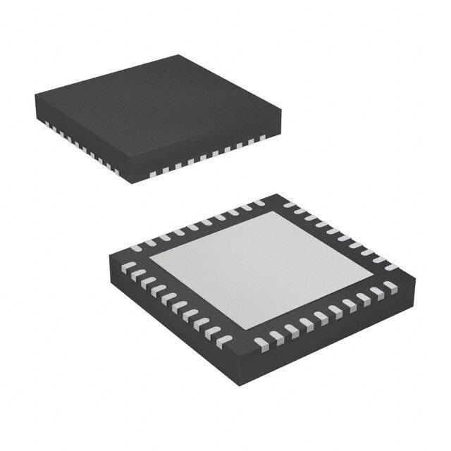
ICGOO电子元器件商城为您提供USB3340-EZK-TR由Microchip设计生产,在icgoo商城现货销售,并且可以通过原厂、代理商等渠道进行代购。 USB3340-EZK-TR价格参考。MicrochipUSB3340-EZK-TR封装/规格:接口 - 驱动器,接收器,收发器, 1/1 Transceiver USB 2.0 32-QFN。您可以下载USB3340-EZK-TR参考资料、Datasheet数据手册功能说明书,资料中有USB3340-EZK-TR 详细功能的应用电路图电压和使用方法及教程。
| 参数 | 数值 |
| 产品目录 | 集成电路 (IC)半导体 |
| 描述 | IC USB 2.0 TXRX 32QFNUSB 接口集成电路 Hi-Speed USB 2.0 flexPWR ULPI Trans |
| 产品分类 | |
| 品牌 | Microchip Technology |
| 产品手册 | |
| 产品图片 |
|
| rohs | 符合RoHS无铅 / 符合限制有害物质指令(RoHS)规范要求 |
| 产品系列 | 接口 IC,USB 接口集成电路,Microchip Technology USB3340-EZK-TRRapidCharge Anywhere™ |
| 数据手册 | |
| 产品型号 | USB3340-EZK-TR |
| PCN组件/产地 | http://www.microchip.com/mymicrochip/NotificationDetails.aspx?id=5836&print=view |
| 产品种类 | USB 接口集成电路 |
| 供应商器件封装 | 32-QFN |
| 其它名称 | 638-1115-1 |
| 包装 | 剪切带 (CT) |
| 协议 | USB 2.0 |
| 双工 | - |
| 商标 | Microchip Technology |
| 安装类型 | 表面贴装 |
| 安装风格 | SMD/SMT |
| 封装 | Reel |
| 封装/外壳 | 32-VFQFN 裸露焊盘 |
| 封装/箱体 | QFN-24 |
| 工作温度 | -40°C ~ 85°C |
| 工作电源电压 | 1.8 V to 3.3 V |
| 工作电源电流 | 1.5 A |
| 工厂包装数量 | 4000 |
| 接口类型 | ULPI |
| 接收器滞后 | 150mV |
| 数据速率 | - |
| 最大工作温度 | + 85 C |
| 最小工作温度 | - 40 C |
| 标准 | USB 2.0 |
| 标准包装 | 1 |
| 电压-电源 | - |
| 类型 | 收发器 |
| 速度 | High-Speed |
| 驱动器/接收器数 | 1/1 |


_renders/CS4265-CNZR.jpg)

- 商务部:美国ITC正式对集成电路等产品启动337调查
- 曝三星4nm工艺存在良率问题 高通将骁龙8 Gen1或转产台积电
- 太阳诱电将投资9.5亿元在常州建新厂生产MLCC 预计2023年完工
- 英特尔发布欧洲新工厂建设计划 深化IDM 2.0 战略
- 台积电先进制程称霸业界 有大客户加持明年业绩稳了
- 达到5530亿美元!SIA预计今年全球半导体销售额将创下新高
- 英特尔拟将自动驾驶子公司Mobileye上市 估值或超500亿美元
- 三星加码芯片和SET,合并消费电子和移动部门,撤换高东真等 CEO
- 三星电子宣布重大人事变动 还合并消费电子和移动部门
- 海关总署:前11个月进口集成电路产品价值2.52万亿元 增长14.8%


PDF Datasheet 数据手册内容提取
USB3340 Enhanced Single Supply Hi-Speed USB ULPI Transceiver Product Features • External Reference Clock operation available - ULPI Clock Input Mode (60MHz sourced by • USB-IF Battery Charging 1.2 Specification Com- Link) pliant - 0 to 3.6V input drive tolerant • Link Power Management (LPM) Specification - Able to accept “noisy” clock sources as refer- Compliant ence to internal, low-jitter PLL • Integrated ESD protection circuits - Crystal support available - Up to ±25kV IEC Air Discharge without exter- • Smart detection circuits allow identification of nal devices USB charger, headset, or data cable insertion • Over-Voltage Protection circuit (OVP) protects the • Includes full support for the optional On-The-Go VBUS pin from continuous DC voltages up to 30V (OTG) protocol detailed in the On-The-Go • Integrated USB Switch SupplementRevision 2.0 specification - Allows single USB port of connection by pro- • Supports the OTG Host Negotiation Protocol viding switching function for: (HNP) and Session Request Protocol (SRP) –Battery charging • UART mode for non-USB serial data transfers –Stereo and mono/mic audio • Internal 5V cable short-circuit protection of ID, DP –USB Full-Speed/Low-Speed data and DM lines to VBUS or ground • RapidCharge Anywhere™ Provides: • Industrial Operating Temperature -40C to +85C - 3-times the charging current through a USB • 32 pin, QFN RoHS Compliant package port over traditional solutions (5 x 5 x 0.90 mm height) - USB-IF Battery Charging 1.2 compliance to any portable device Applications - Charging current up to 1.5Amps via compati- ble USB host or dedicated charger The USB3340 is the solution of choice for any applica- - Dedicated Charging Port (DCP), Charging tion where a Hi-Speed USB connection is desired and (CDP) & Standard (SDP) Downstream Port when board space, power, and interface pins must be support minimized. • flexPWR® Technology - Extremely low current design ideal for battery • Cell Phones powered applications • PDAs - “Sleep” mode tri-states all ULPI pins and • MP3 Players places the part in a low current state • GPS Personal Navigation - 1.8V to 3.3V IO Voltage • Scanners • Single Power Supply Operation • External Hard Drives - Integrated 1.8V regulator • Digital Still and Video Cameras - Integrated 3.3V regulator • Portable Media Players –100mV dropout voltage • Entertainment Devices • PHYBoost • Printers - Programmable USB transceiver drive • Set Top Boxes strength for recovering signal integrity • Video Record/Playback Systems • VariSense™ • IP and Video Phones - Programmable USB receiver sensitivity • Gaming Consoles • “Wrapper-less” design for optimal timing perfor- mance and design ease - Low Latency Hi-Speed Receiver (43 Hi- Speed clocks Max) allows use of legacy UTMI Links with a ULPI bridge 2009-2019 Microchip Technology Inc. DS00001678D-page 1
USB3340 TO OUR VALUED CUSTOMERS It is our intention to provide our valued customers with the best documentation possible to ensure successful use of your Microchip products. To this end, we will continue to improve our publications to better suit your needs. Our publications will be refined and enhanced as new volumes and updates are introduced. If you have any questions or comments regarding this publication, please contact the Marketing Communications Department via E-mail at docerrors@microchip.com. We welcome your feedback. Most Current Data Sheet To obtain the most up-to-date version of this data sheet, please register at our Worldwide Web site at: http://www.microchip.com You can determine the version of a data sheet by examining its literature number found on the bottom outside corner of any page. The last character of the literature number is the version number, (e.g., DS30000000A is version A of document DS30000000). Errata An errata sheet, describing minor operational differences from the data sheet and recommended workarounds, may exist for cur- rent devices. As device/documentation issues become known to us, we will publish an errata sheet. The errata will specify the revision of silicon and revision of document to which it applies. To determine if an errata sheet exists for a particular device, please check with one of the following: • Microchip’s Worldwide Web site; http://www.microchip.com • Your local Microchip sales office (see last page) When contacting a sales office, please specify which device, revision of silicon and data sheet (include -literature number) you are using. Customer Notification System Register on our web site at www.microchip.com to receive the most current information on all of our products. DS00001678D-page 2 2009-2019 Microchip Technology Inc.
USB3340 Table of Contents 1.0 General Description ........................................................................................................................................................................4 2.0 Pin Locations and Definitions ..........................................................................................................................................................6 3.0 Limiting Values ................................................................................................................................................................................9 4.0 Electrical Characteristics ...............................................................................................................................................................10 5.0 Architecture Overview ...................................................................................................................................................................18 6.0 ULPI Operation .............................................................................................................................................................................36 7.0 ULPI Register Map ........................................................................................................................................................................57 8.0 Application Notes ..........................................................................................................................................................................71 9.0 Package Outline ............................................................................................................................................................................76 Appendix A: Data sheet Revision History ...........................................................................................................................................78 2009-2019 Microchip Technology Inc. DS00001678D-page 3
USB3340 1.0 GENERAL DESCRIPTION Microchip’s USB3340 is a Hi-Speed USB 2.0 Transceiver that provides a physical layer (PHY) solution well-suited for portable electronic devices. Both commercial and industrial temperature applications are supported. the Several advanced features make the USB3340 the transceiver of choice by reducing both eBOM part count and printed circuit board (PCB) area. Outstanding ESD robustness eliminates the need for external ESD protection devices in typical applications. The internal Over-Voltage Protection circuit (OVP) protects the USB3340 from voltages up to 30V on the VBUS pin. By using a reference clock from the Link, the USB3340 removes the cost of a dedicated crystal ref- erence from the design. The USB3340 includes integrated 3.3V and 1.8V regulators, making it possible to operate the device from a single power supply. The USB3340 is optimized for use in portable applications where a low operating current and standby currents are essential. The USB3340 operates from a single supply and includes integrated regulators for its supplies. The USB3340 also supports the USB Link Power Management protocol (LPM) to further reduce USB operating currents. The USB3340 also includes RapidCharge Anywhere which supports USB-IF Battery Charging 1.2 for any portable device. RapidCharge Anywhere provides three times the charging current through a USB port over traditional solutions which translate up to 1.5Amps via compatible USB host or dedicated charger. In addition, this provides a complete USB charging ecosystem between device and host ports such as Dedicated Charging Port (DCP), Charging (CDP) and Stan- dard (SDP) Downstream Ports. Section 5.9, "USB Charger Detection Support," on page32 describes this is further detail. The USB3340 meets all of the electrical requirements for a Hi-Speed USB Host, Device, or an On-the-Go (OTG) trans- ceiver. In addition to the supporting USB signaling, the USB3340 also provides USB UART mode and, in versions with the integrated USB switch, USB Audio mode. USB3340 uses the industry standard UTMI+ Low Pin Interface (ULPI) to connect the USB transceiver to the Link. ULPI uses a method of in-band signaling and status byte transfers between the Link and PHY to facilitate a USB session with only twelve pins. The USB3340 uses “wrapper-less” technology to implement the ULPI interface. This “wrapper-less” technology allows the PHY to achieve a low latency transmit and receive time. Microchip’s low latency transceiver allows an existing UTMI Link to be reused by adding a UTMI to ULPI bridge. By adding a bridge to the ASIC the existing and proven UTMI Link IP can be reused. The integrated USB switch enables a single USB port of connection. DS00001678D-page 4 2009-2019 Microchip Technology Inc.
USB3340 FIGURE 1-1: BLOCK DIAGRAM USB3340 XI 0] K / L[2: L E C S F F E O E R X R CPEN VBUS OVP Low Jitter BIAS RBIAS n OTG Integrated o ID cti PLL e ot Pr Integrated RESETB D Power VBAT DP S Hi-Speed VDD33 E Management BC 1.1 USB VDD18 DM ULPI Transceiver Registers VDDIO and State STP Machine ULPI NXT Interface DIR USB DP/DM CLKOUT Switch L R DATA[7:0] _ _ K K P P S S In USB audio mode, a switch connects the DP pin to the SPK_R pin, and another switch connects he DM pin to the SPK_L pin. These switches are shown in the lower left-hand corner of .The USB3340 can be configured to enter USB audio mode as described in Section 6.7.2, "USB Audio Mode," on page55. In addition, these switches are on when the RESETB pin of the USB3340 is asserted. The USB audio mode enables audio signaling from a single USB port of con- nection, and the switches may also be used to connect Full Speed USB from another transceiver to the USB connector. The USB3340 includes an integrated 3.3V LDO regulator that is used to generate 3.3V from power applied to the VBAT pin. The voltage on the VBAT pin can range from 3.0 to 5.5V. The regulator dropout voltage is less than 100mV which allows the PHY to continue USB signaling when the voltage on VBAT drops to 3.0V. The USB transceiver will continue to operate at lower voltages, although some parameters may be outside the limits of the USB specifications. The VBAT and VDD33 pins should never be connected together. In USB UART mode, the USB3340 DP and DM pins are redefined to enable pass-through of asynchronous serial data. The USB3340 will enter UART mode when programmed, as described in Section 6.7.1, "Entering USB UART Mode," on page54. 2009-2019 Microchip Technology Inc. DS00001678D-page 5
USB3340 2.0 PIN LOCATIONS AND DEFINITIONS 2.1 USB3340 Pin Locations and Descriptions 2.1.1 USB3340 PIN DIAGRAM AND PIN DEFINITIONS The illustration below is viewed from the top of the package. FIGURE 2-1: USB3340 PIN LOCATIONS - TOP VIEW B K O 8 T L VDDI DIR NC STP VDD1 RESE REFC XO 2 1 0 9 8 7 6 5 3 3 3 2 2 2 2 2 CLKOUT 1 24 RBIAS NXT 2 23 ID DATA0 3 22 VBUS USB3300 DATA1 4 Hi3-S2p Peiend Q UFSNB2 21 VBAT U5LxP5I mPHmY DATA2 5 20 VDD33 32 Pin QFN DATA3 6 19 DM DATA4 7 18 DP GND FLAG REFSEL[0] 8 17 CPEN 0 1 2 3 4 5 6 9 1 1 1 1 1 1 1 TA5 TA6 L[1] NC TA7 L[2] K_L K_R A A E A E P P D D S D S S S F F E E R R The following table details the pin definitions for the figure above. TABLE 2-1: USB3340 PIN DESCRIPTIONS Direction/ Active Pin Name Description Type Level 1 CLKOUT Output, N/A ULPI Clock Out Mode: CMOS 60MHz ULPI clock output. All ULPI signals are driven synchronous to the rising edge of this clock. ULPI Clock In Mode: Connect this pin to VDDIO to configure 60MHz ULPI Clock IN mode as described in Section 5.5.1, "REFCLK Frequency Selection," on page21. 2 NXT Output, High The PHY asserts NXT to throttle the data. When the CMOS Link is sending data to the PHY, NXT indicates when the current byte has been accepted by the PHY. 3 DATA[0] I/O, N/A ULPI bi-directional data bus. DATA[0] is the LSB. CMOS DS00001678D-page 6 2009-2019 Microchip Technology Inc.
USB3340 TABLE 2-1: USB3340 PIN DESCRIPTIONS (CONTINUED) Direction/ Active Pin Name Description Type Level 4 DATA[1] I/O, N/A ULPI bi-directional data bus. CMOS 5 DATA[2] I/O, N/A ULPI bi-directional data bus. CMOS 6 DATA[3] I/O, N/A ULPI bi-directional data bus. CMOS 7 DATA[4] I/O, N/A ULPI bi-directional data bus. CMOS 8 Input N/A Used to select xtal/reference frequency. This pad is REFSEL[0] connected to VDDIO or GND. 9 DATA[5] I/O, N/A ULPI bi-directional data bus. CMOS 10 DATA[6] I/O, N/A ULPI bi-directional data bus. CMOS 11 Input N/A Used to select xtal/reference frequency. This pad is REFSEL[1] connected to VDDIO or GND. 12 NC N/A N/A No connect. Leave pin floating. 13 DATA[7] I/O, N/A ULPI bi-directional data bus. DATA[7] is the MSB. CMOS 14 Input N/A Used to select xtal/reference frequency. This pad is REFSEL[2] connected to VDDIO or GND. 15 SPK_L I/O, N/A USB switch in/out for DM signals. Analog 16 SPK_R I/O, N/A USB switch in/out for DP signals. Analog 17 Output, High External 5 volt supply enable. This pin is used to CMOS enable the external Vbus power supply. The CPEN CPEN pin is low on POR. This pad uses VDD33 logic level. 18 DP I/O, N/A D+ pin of the USB cable. Analog 19 DM I/O, N/A D- pin of the USB cable. Analog 20 VDD33 Power N/A 3.3V Regulator Output. A 1.0 µF (<1Ω ESR) bypass capacitor to ground is required for regulator stability. The bypass capacitor should be placed as close as possible to the USB3340. 21 VBAT Power N/A Regulator input. The regulator supply can be from 5.5V to 3.0V. 22 VBUS I/O, N/A This pin is used for the VBUS comparator inputs and Analog for VBUS pulsing during session request protocol. An external resistor, R , is required between this VBUS pin and the USB connector. 2009-2019 Microchip Technology Inc. DS00001678D-page 7
USB3340 TABLE 2-1: USB3340 PIN DESCRIPTIONS (CONTINUED) Direction/ Active Pin Name Description Type Level 23 ID Input, N/A For device applications the ID pin is connected to Analog VDD33. For Host applications ID is grounded. For OTG applications the ID pin is connected to the USB connector. 24 RBIAS Analog, N/A Bias Resistor pin. This pin requires an 8.06kΩ CMOS (±1%) resistor to ground, placed as close as possible to the USB3340. Nominal voltage during ULPI operation is 0.8V. 25 Output, N/A Crystal pin. If using an external clock on XI this pin XO Analog should be floated. 26 REFCLK Input, N/A ULPI Clock Out Mode: CMOS Model-specific reference clock or XI (crystal in) pin. See Examplea, Product Identification System on page 80. ULPI Clock In Mode: 60MHz ULPI clock input. 27 RESETB Input, Low When low, the part is suspended and the 3.3V and CMOS, 1.8V regulators are disabled. When high, the USB3340 will operate as a normal ULPI device, as described in Section 5.6.2, "Power On Reset (POR)," on page25. The state of this pin may be changed asynchronously to the clock signals. When asserted for a minimum of 1 microsecond and then de- asserted, the ULPI registers are reset to their default state and all internal state machines are reset. 28 VDD18 Power N/A 1.8V Regulator Output. A 1.0 µF (<1Ω ESR) bypass capacitor to ground is required for regulator stability. The bypass capacitor should be placed as close as possible to the USB3340. 29 STP Input, High The Link asserts STP for one clock cycle to stop the CMOS data stream currently on the bus. If the Link is sending data to the PHY, STP indicates the last byte of data was on the bus in the previous cycle. 30 NC N/A N/A No connect. 31 DIR Output, N/A Controls the direction of the data bus. When the PHY CMOS has data to transfer to the Link, it drives DIR high to take ownership of the bus. When the PHY has no data to transfer it drives DIR low and monitors the bus for commands from the Link. 32 Power N/A ULPI interface supply voltage. When RESETB is low VDDIO and VDDIO is powered on, ULPI pins will tri-state. FLAG GND Ground N/A Ground. DS00001678D-page 8 2009-2019 Microchip Technology Inc.
USB3340 3.0 LIMITING VALUES 3.1 Absolute Maximum Ratings TABLE 3-1: ABSOLUTE MAXIMUM RATINGS Parameter Symbol Conditions MIN TYP MAX Units VBUS, VBAT, ID, DP, DM, V Voltage measured at pin. -0.5 +6.0 V MAX_5V SPK_L, and SPK_R VBUS tolerant to 30V with voltage to GND external R . VBUS Maximum VDD18 voltage V -0.5 2.5 V MAX_18V to Ground Maximum VDD33 voltage V -0.5 4.0 V MAX_33V to Ground Maximum VDDIO voltage V -0.5 4.0 V MAX_IOV to Ground Maximum I/O voltage to V -0.5 V + 0.7 MAX_IN DDIO Ground Operating Temperature T -40 85 C MAX_OP Storage Temperature T -55 150 C MAX_STG Note: Stresses beyond those listed under “Absolute Maximum Ratings” may cause permanent damage to the device. Exposure to absolute maximum rating conditions for extended periods may affect device reliability. 3.2 Recommended Operating Conditions TABLE 3-2: RECOMMENDED OPERATING CONDITIONS Parameter Symbol Conditions MIN TYP MAX Units VBAT to GND V 3.0 5.5 V BAT VDD33 to GND V 3.0 3.3 3.6 V DD33 VDD18 to GND V 1.6 1.8 2.0 V DD18 VDDIO to GND V 1.6 1.8-3.3 3.6 V DDIO Input Voltage on Digital V 0.0 V V I DDIO Pins (RESETB, STP, DIR, NXT, DATA[7:0]) Voltage on Analog I/O V 0.0 V V I(I/O) DD33 Pins (DP, DM, ID, CPEN, SPK_L, SPK_R) VBUS to GND V 0.0 5.5 V VMAX Ambient Temperature T -40 85 C A 2009-2019 Microchip Technology Inc. DS00001678D-page 9
USB3340 4.0 ELECTRICAL CHARACTERISTICS The following conditions are assumed unless otherwise specified: V = 3.0 to 3.6V; VDD18 = 1.6 to 2.0V; V = 0V; T = -40C to +85C DD33 SS A 4.1 Operating Current TABLE 4-1: OPERATING CURRENT Parameter Symbol Conditions MIN TYP MAX Units Synchronous Mode Current I USB Idle 18 22 24 mA VBAT(SYNC) (Default Configuration) I 1 2 5 mA VIO(SYNC) Synchronous Mode Current I Active USB Transfer 33 35 37 mA VBAT(HS) (HS USB operation) I 5 6 14 mA VIO(HS) Synchronous Mode Current I Active USB Transfer 25 28.5 30 mA VBAT(FS) (FS/LS USB operation) I 4 5 13 mA VIO(FS) Serial Mode Current I 7 8 9 mA VBAT(FS_S) (FS/LS USB) Note 4-1 I 0 0.1 0.7 mA VIO(FS_S) USB UART Current I 7 8 9 mA VBAT(UART) Note 4-1 I 0 0.1 0.7 mA VIO(UART) Low Power Mode I V = 4.2V 29 32 83 uA VBAT(SUSPEND) VBAT Note 4-2 V 1.8V VDDIO = Note 4-3 I 0 0 2 uA VIO(SUSPEND) RESET Mode I RESETB = 0 0.1 1 12 uA VBAT(RSTB) Note 4-3 V = 4.2V VBAT IVIO(RSTB) VVDDIO = 1.8V 0 0 7 uA Note 4-1 ClockSuspendM bit = 0. Note 4-2 SessEnd, VbusVld, and IdFloat comparators disabled. STP Interface protection disabled. Note 4-3 REFCLK is OFF 4.2 Clock Specifications The model number for each frequency of REFCLK is provided in "Product Identification System". TABLE 4-2: CLOCK SPECIFICATIONS Parameter Symbol Conditions MIN TYP MAX Units Suspend Recovery Time T LPM Enable = 0 1.0 1.1 1.2 ms START T LPM Enable = 1 125 150 uS START_LPM PHY Preparation Time T LPM Enable = 0 1.0 1.1 1.2 ms PREP 60MHz REFCLK T LPM Enable = 1 125 150 uS PREP_LPM DS00001678D-page 10 2009-2019 Microchip Technology Inc.
USB3340 TABLE 4-2: CLOCK SPECIFICATIONS (CONTINUED) Parameter Symbol Conditions MIN TYP MAX Units CLKOUT Duty Cycle DC ULPI Clock Input Mode 45 55 % CLKOUT REFCLK Duty Cycle DC 20 80 % REFCLK REFCLK Frequency Accuracy F -500 +500 PPM REFCLK Note: • T and T are measured from the time when REFCLK and RESETB are both valid to when the START PREP USB3340 de-asserts DIR. • The USB3340 uses the AutoResume feature, Section 6.4.1.4, "Host Resume K," on page47, to allow a host start-up time of less than 1ms. 4.3 ULPI Interface Timing TABLE 4-3: ULPI INTERFACE TIMING Parameter Symbol Conditions MIN MAX Units 60MHz ULPI Output Clock Note 4-4 Setup time (STP, data in) T , T Model-specific REFCLK 5.0 ns SC SD Hold time (STP, data in) T , T Model-specific REFCLK 0.0 ns HC HD Output delay (control out, 8-bit data out) T , T Model-specific REFCLK 1.5 6 ns DC DD 60MHz ULPI Input Clock Setup time (STP, data in) T , T 60MHz REFCLK 3 ns SC SD Hold time (STP, data in) T , T 60MHz REFCLK 0 ns HC HD Output delay (control out, 8-bit data out) T , T 60MHz REFCLK 0.5 6.0 ns DC DD Note: C = 10pF Load Note 4-4 REFCLK does not need to be aligned in any way to the ULPI signals. 4.4 Digital IO Pins TABLE 4-4: DIGITAL IO CHARACTERISTICS: RESETB, CPEN, STP, DIR, NXT, DATA[7:0], AND REFCLK PINS Parameter Symbol Conditions MIN TYP MAX Units Low-Level Input Voltage V V 0.8 V IL SS High-Level Input Voltage V 0.68 * V V IH DDIO V DDIO High-Level Input Voltage V 0.68 * V V IH_REF DD33 REFCLK and RESETB V DDIO Low-Level Output Voltage V I = 8mA 0.4 V OL OL High-Level Output Voltage V I = -8mA V - V OH OH DDIO 0.4 2009-2019 Microchip Technology Inc. DS00001678D-page 11
USB3340 TABLE 4-4: DIGITAL IO CHARACTERISTICS: RESETB, CPEN, STP, DIR, NXT, DATA[7:0], AND REFCLK PINS (CONTINUED) Parameter Symbol Conditions MIN TYP MAX Units High-Level Output Voltage V I = -8mA V V OH OH DD33 CPEN - 0.4 Output rise time T C = 10pF 1.19 nS IORISE LOAD Output fall time T C = 10pF 1.56 nS IOFALL LOAD Input Leakage Current I ±10 uA LI Pin Capacitance Cpin 4 pF STP pull-up resistance R InterfaceProtectDisable = 55 67 80 kΩ STP 0 DATA[7:0] pull-down R ULPI Synchronous Mode 55 67 77 kΩ DATA_PD resistance CLKOUT External Drive V At start-up or following 0.4 * V IH_ED reset V DDIO 4.5 DC Characteristics: Analog I/O Pins TABLE 4-5: DC CHARACTERISTICS: ANALOG I/O PINS (DP/DM) Parameter Symbol Conditions MIN TYP MAX Units LS/FS FUNCTIONALITY Input levels Differential Receiver Input V | V(DP) - V(DM) | 0.2 V DIFS Sensitivity Differential Receiver V 0.8 2.5 V CMFS Common-Mode Voltage Single-Ended Receiver Low V Note 4-6 0.8 V ILSE Level Input Voltage Single-Ended Receiver High V Note 4-6 2.0 V IHSE Level Input Voltage Single-Ended Receiver V 0.050 0.150 V HYSSE Hysteresis Output Levels Low Level Output Voltage V Pull-up resistor on DP; 0.3 V FSOL R = 1.5kΩ to V L DD33 High Level Output Voltage V Pull-down resistor on DP, 2.8 3.6 V FSOH DM; Note 4-6 R = 15kΩ to GND L Termination Driver Output Impedance for Z Steady state drive 40.5 45 49.5 Ω HSDRV HS Input Impedance Z RX, RPU, RPD disabled 1.0 MΩ INP DS00001678D-page 12 2009-2019 Microchip Technology Inc.
USB3340 TABLE 4-5: DC CHARACTERISTICS: ANALOG I/O PINS (DP/DM) (CONTINUED) Parameter Symbol Conditions MIN TYP MAX Units Pull-up Resistor Impedance R Bus Idle, Note 4-5 0.900 1.24 1.575 kΩ PU Pull-up Resistor Impedance R Device Receiving, Note 4- 1.425 2.26 3.09 kΩ PU 5 Pull-dn Resistor Impedance R Note 4-5 14.25 16.9 20 kΩ PD HS FUNCTIONALITY Input levels HS Differential Input V | V(DP) - V(DM) | 100 mV DIHS Sensitivity HS Data Signaling Common V -50 500 mV CMHS Mode Voltage Range HS Squelch Detection V VariSense[1:0] = 00b 100 150 mV HSSQ Threshold (Differential) Note 4-7 HS Disconnect Threshold V 525 625 mV HSDSC Output Levels High Speed Low Level V 45Ω load -10 10 mV HSOL Output Voltage (DP/DM referenced to GND) High Speed High Level V 45Ω load 360 440 mV HSOH Output Voltage (DP/DM referenced to GND) High Speed IDLE Level V 45Ω load -10 10 mV OLHS Output Voltage (DP/DM referenced to GND) Chirp-J Output Voltage V HS termination resistor 700 1100 mV CHIRPJ (Differential) disabled, pull-up resistor connected. 45Ω load. Chirp-K Output Voltage V HS termination resistor -900 -500 mV CHIRPK (Differential) disabled, pull-up resistor connected. 45Ω load. Leakage Current OFF-State Leakage Current I ±10 uA LZ Port Capacitance Transceiver Input C Pin to GND 5 10 pF IN Capacitance Note 4-5 The resistor value follows the 27% Resistor ECN published by the USB-IF. Note 4-6 The values shown are valid when the USB RegOutput bits in the USB IO & Power Management register are set to the default value. Note 4-7 An automatic waiver up to 200mV is granted to accommodate system-level elements such as measurement/test fixtures, captive cables, EMI components, and ESD suppression. This parameter can be tuned using VariSense technology, as defined in Section 7.1.3.1, "HS Compensation Register," on page66 of Section7.0, ULPI Register Map. 2009-2019 Microchip Technology Inc. DS00001678D-page 13
USB3340 4.6 Dynamic Characteristics: Analog I/O Pins TABLE 4-6: DYNAMIC CHARACTERISTICS: ANALOG I/O PINS (DP/DM) Parameter Symbol Conditions MIN TYP MAX Units FS Output Driver Timing FS Rise Time T C = 50pF; 10 to 90% of 4 20 ns FR L |V - V | OH OL FS Fall Time T C = 50pF; 10 to 90% of 4 20 ns FF L |V - V | OH OL Output Signal Crossover V Excluding the first 1.3 2.0 V CRS Voltage transition from IDLE state Differential Rise/Fall Time T Excluding the first 90 111.1 % FRFM Matching transition from IDLE state LS Output Driver Timing LS Rise Time T C = 50-600pF; 75 300 ns LR L 10 to 90% of |V - V | OH OL LS Fall Time T C = 50-600pF; 75 300 ns LF L 10 to 90% of |V - V | OH OL Differential Rise/Fall Time T Excluding the first 80 125 % LRFM Matching transition from IDLE state HS Output Driver Timing Differential Rise Time T 500 ps HSR Differential Fall Time T 500 ps HSF Driver Waveform Eye pattern of Template 1 Requirements in USB 2.0 specification High Speed Mode Timing Receiver Waveform Eye pattern of Template 4 Requirements in USB 2.0 specification Data Source Jitter and Eye pattern of Template 4 Receiver Jitter Tolerance in USB 2.0 specification 4.7 VBUS Electrical Characteristics TABLE 4-7: VBUS ELECTRICAL CHARACTERISTICS Parameter Symbol Conditions MIN TYP MAX Units SessEnd trip point V 0.2 0.5 0.8 V SessEnd SessVld trip point V 0.8 1.4 2.0 V SessVld VbusVld trip point V 4.4 4.58 4.75 V VbusVld VBUS Pull-Up R VBUS to VDD33 Note 4-8 1.29 1.34 1.45 kΩ VPU (ChargeVbus = 1) DS00001678D-page 14 2009-2019 Microchip Technology Inc.
USB3340 TABLE 4-7: VBUS ELECTRICAL CHARACTERISTICS (CONTINUED) Parameter Symbol Conditions MIN TYP MAX Units VBUS Pull-down R VBUS to GND Note 4-8 1.55 1.7 1.85 kΩ VPD (DisChargeVbus = 1) VBUS Impedance R VBUS to GND 40 75 100 kΩ VB A-Device Impedance to R Maximum Impedance to 100 kΩ IdGnd ground ground on ID pin Note 4-8 The R and R values include the required 1kΩ external R resistor. VPD VPU VBUS 4.8 ID Electrical Characteristics TABLE 4-8: ID ELECTRICAL CHARACTERISTICS Parameter Symbol Conditions MIN TYP MAX Units ID Ground Trip Point V 0.4 0.7 0.9 V IdGnd ID Float Trip Point V 1.6 2.2 2.5 V IdFloat ID pull-up resistance R IdPullup = 1 80 100 120 kΩ ID ID weak pull-up resistance R IdPullup = 0 1 MΩ IDW ID pull-dn resistance R IdGndDrv = 1 1000 Ω IDPD 4.9 USB Audio Switch Characteristics TABLE 4-9: USB AUDIO SWITCH CHARACTERISTICS Parameter Symbol Conditions MIN TYP MAX Units Minimum “ON” Resistance R 0 < V < V 2.7 5 5.8 Ω ON_Min switch DD33 Maximum “ON” Resistance R 0 < V < V 4.5 7 13 Ω ON_Max switch DD33 Minimum “OFF” R 0 < V < V 1 MΩ OFF_Min switch DD33 Resistance 4.10 USB Charger Detection Characteristics TABLE 4-10: USB CHARGER DETECTION CHARACTERISTICS Parameter Symbol Conditions MIN TYP MAX Units Data Source Voltage V I < 250uA 0.5 0.7 V DAT_SRC DAT_SRC Data Detect Voltage V 0.25 0.4 V DAT_REF Data Source Current I 250 uA DAT_SRC Data Sink Current I 50 150 uA DAT_SINK 2009-2019 Microchip Technology Inc. DS00001678D-page 15
USB3340 TABLE 4-10: USB CHARGER DETECTION CHARACTERISTICS (CONTINUED) Parameter Symbol Conditions MIN TYP MAX Units Data Connect Current I 7 13 uA DP_SRC Weak Pull-up Resistor R Configured by bits 4 and 5 128 170 212 kΩ CD Impedance in USB IO & Power Management register. 4.11 Regulator Output Voltages and Capacitor Requirement TABLE 4-11: REGULATOR OUTPUT VOLTAGES AND CAPACITOR REQUIREMENT Parameter Symbol Conditions MIN TYP MAX Units Regulator Output Voltage V 5.5V > VBAT > 3.0V 2.8 3.3 3.6 V DD33 USB UART Mode & UART 2.7 3.0 3.3 V RegOutput[1:0] = 01 6V > VBAT > 3.0V USB UART Mode & UART 2.47 2.75 3.03 V RegOutput[1:0] = 10 6V > VBAT > 3.0V USB UART Mode & UART 2.25 2.5 2.75 V RegOutput[1:0] = 11 6V > VBAT > 3.0V Regulator Bypass Capacitor C 1.0 µF OUT33 Bypass Capacitor ESR C 1 Ω ESR33 Regulator Output Voltage V 3.6V > VDD33 > 2.25V 1.6 1.8 2.0 V DD18 Regulator Bypass Capacitor C 1.0 µF OUT18 Bypass Capacitor ESR C 1 Ω ESR18 4.12 Piezoelectric Resonator for Internal Oscillator The internal oscillator may be used with an external quartz crystal or ceramic resonator as described in Section 5.4, "Crystal Reference Support," on page21. See Table4-12 for the recommended crystal specifications. TABLE 4-12: USB3340 QUARTZ CRYSTAL SPECIFICATIONS Parameter Symbol MIN NOM MAX Units Notes Crystal Cut AT, typ Crystal Oscillation Mode Fundamental Mode Crystal Calibration Mode Parallel Resonant Mode Frequency F - See - MHz fund Product Identificati on System on page 80 Total Allowable PPM Budget - - ±500 PPM Note 4-9 Shunt Capacitance C - 7 typ - pF O Load Capacitance C - 20 typ - pF L DS00001678D-page 16 2009-2019 Microchip Technology Inc.
USB3340 TABLE 4-12: USB3340 QUARTZ CRYSTAL SPECIFICATIONS (CONTINUED) Parameter Symbol MIN NOM MAX Units Notes Drive Level P 0.1 - - mW W Equivalent Series Resistance R - - 30 Ω 1 USB3340 REFCLK Pin - 3 typ - pF Note 4-10 Capacitance USB3340 XO Pin Capacitance - 3 typ - pF Note 4-10 Note 4-9 The required bit rate accuracy for Hi-Speed USB applications is ±500 ppm as provided in the USB 2.0 Specification. This takes into account the effect of voltage, temperature, aging, etc. Note 4-10 This number includes the pad, the bond wire and the lead frame. Printed Circuit Board (PCB) capacitance is not included in this value. The PCB capacitance value and the capacitance value of the XO and REFCLK pins are required to accurately calculate the value of the two external load capacitors. 4.13 ESD and Latch-Up Performance TABLE 4-13: ESD AND LATCH-UP PERFORMANCE Parameter Conditions MIN TYP MAX Units Comments ESD PERFORMANCE Note 4-11 Human Body Model ±8 kV Device Note 4-12 System EN/IEC 61000-4-2 Contact ±25 kV 3rd party system test Discharge System EN/IEC 61000-4-2 Air-gap ±25 kV 3rd party system test Discharge LATCH-UP PERFORMANCE All Pins EIA/JESD 78, Class II 150 mA Note 4-11 REFCLK, XO , ID, RESETB, SPK_L and SPK_Rpins: ±5kV Human Body Model. Note 4-12 The REFSEL[2:0] pins only tested to ±2kV Human Body Model. 2009-2019 Microchip Technology Inc. DS00001678D-page 17
USB3340 5.0 ARCHITECTURE OVERVIEW The USB3340 consists of the blocks shown in the diagram below. FIGURE 5-1: USB3340 SYSTEM DIAGRAM DrvVbus or’d with DrvVbusExternal DATA7 VDD33 DATA6 CPEN IdGnd DATA5 RIDW RID IdFloat O DDAATTAA43 ID VDD33 Rid Value odule DUigLiPtiaI l gital I DDDAAATTTAAA201 VVBBUAST OVP RVPU SessEnd OTG M Di DNSTIXRPT on LDO SessValid CRLEKSOEUTBT VDD33 rotecti LDO RVB RVPD VbusValid X Data X Data VDDIO P T R VDD18 D VDD33 S REFCLK / XI E Integrated XO RCD RCD RPU RPU HS/FS/LS Low Jitter REFSEL0 TX PLL REFSEL1 DP TX Encoding REFSEL2 DM HS/FS/LS RX BIAS RBIAS SPK_L RPD RPD RX Decoding SPK_R 5.1 ULPI Digital Operation and Interface This section of the USB3340 is covered in detail in Section 6.0, "ULPI Operation". 5.2 USB 2.0 Hi-Speed Transceiver The blocks in the lower left-hand corner of interface to the DP/DM pins. 5.2.1 USB TRANSCEIVER The USB3340 transceiver includes a Universal Serial Bus Specification Rev 2.0 compliant receiver and transmitter. The DP/DM signals in the USB cable connect directly to the receivers and transmitters. The receiver consists of receivers for HS and FS/LS mode. Depending on the mode, the selected receiver provides the serial data stream through the multiplexer to the RX Logic block. For HS mode support, the HS RX block contains a squelch circuit to insure that noise is not interpreted as data. The RX block also includes a single-ended receiver on each of the data lines to determine the correct FS linestate. Data from the Link is encoded, bit stuffed, serialized and transmitted onto the USB cable by the transmitter. Separate differential FS/LS and HS transmitters are included to support all modes. The USB3340 TX block meets the HS signaling level requirements in the USB 2.0 Specification when the PCB traces from the DP and DM pins to the USB connector are correctly designed. In some systems the proper 90Ω differential impedance can not be maintained and it may be desirable to compensate for loss by adjusting the HS transmitter ampli- DS00001678D-page 18 2009-2019 Microchip Technology Inc.
USB3340 tude and this HS squelch threshold. The PHYBoost bits in the HS Compensation Register may be configured to adjust the HS transmitter amplitude at the DP and DM pins. The VariSense bits in the HS Compensation Register can also be used to lower the squelch threshold to compensate for losses on the PCB. To ensure proper operation of the USB transceiver the settings of Table5-1 must be followed. 5.2.2 TERMINATION RESISTORS The USB3340 transceiver fully integrates all of the USB termination resistors on both DP and DM. This includes 1.5kΩ pull-up resistors, 15kΩ pull-down resistors and the 45Ω High Speed termination resistors. These resistors require no tuning or trimming by the Link. The state of the resistors is determined by the operating mode of the transceiver when operating in synchronous mode. The XcvrSelect[1:0], TermSelect and OpMode[1:0] bits in the Function Control register, and the DpPulldown and DmPulldown bits in the OTG Control register control the configuration of the termination resistors. All possible valid resistor combinations are shown in Table5-1, and operation is supported in only the configurations shown. If a ULPI Register Setting is configured that does not match a setting in the table, the transceiver operation is not maintained and the settings in the last row of Table5-1 will be used. • RPU_DP_EN activates the 1.5kΩ DP pull-up resistor • RPU_DM_EN activates the 1.5kΩ DM pull-up resistor • RPD_DP_EN activates the 15kΩ DP pull-down resistor • RPD_DM_EN activates the 15kΩ DM pull-down resistor • HSTERM_EN activates the 45Ω DP and DM High Speed termination resistors TABLE 5-1: DP/DM TERMINATION VS. SIGNALING MODE USB3340 Termination ULPI Register Settings Resistor Settings Signaling Mode cvrSelect[1:0] TermSelect OpMode[1:0] DpPulldown DmPulldown RPU_DP_EN RPU_DM_EN RPD_DP_EN RPD_DM_EN HSTERM_EN X General Settings Tri-State Drivers, Note 5-1 XXb Xb 01b Xb Xb 0b 0b 0b 0b 0b Power-up or VBUS < V 01b 0b 00b 1b 1b 0b 0b 1b 1b 0b SESSEND Host Settings Host Chirp 00b 0b 10b 1b 1b 0b 0b 1b 1b 1b Host High Speed 00b 0b 00b 1b 1b 0b 0b 1b 1b 1b Host Full Speed X1b 1b 00b 1b 1b 0b 0b 1b 1b 0b Host HS/FS Suspend 01b 1b 00b 1b 1b 0b 0b 1b 1b 0b Host HS/FS Resume 01b 1b 10b 1b 1b 0b 0b 1b 1b 0b Host Low Speed 10b 1b 00b 1b 1b 0b 0b 1b 1b 0b Host LS Suspend 10b 1b 00b 1b 1b 0b 0b 1b 1b 0b Host LS Resume 10b 1b 10b 1b 1b 0b 0b 1b 1b 0b Host Test J/Test_K 00b 0b 10b 1b 1b 0b 0b 1b 1b 1b Peripheral Settings 2009-2019 Microchip Technology Inc. DS00001678D-page 19
USB3340 TABLE 5-1: DP/DM TERMINATION VS. SIGNALING MODE (CONTINUED) USB3340 Termination ULPI Register Settings Resistor Settings Signaling Mode cvrSelect[1:0] TermSelect OpMode[1:0] DpPulldown DmPulldown RPU_DP_EN RPU_DM_EN RPD_DP_EN RPD_DM_EN HSTERM_EN X Peripheral Chirp 00b 1b 10b 0b 0b 1b 0b 0b 0b 0b Peripheral HS 00b 0b 00b 0b 0b 0b 0b 0b 0b 1b Peripheral FS 01b 1b 00b 0b 0b 1b 0b 0b 0b 0b Peripheral HS/FS Suspend 01b 1b 00b 0b 0b 1b 0b 0b 0b 0b Peripheral HS/FS Resume 01b 1b 10b 0b 0b 1b 0b 0b 0b 0b Peripheral LS 10b 1b 00b 0b 0b 0b 1b 0b 0b 0b Peripheral LS Suspend 10b 1b 00b 0b 0b 0b 1b 0b 0b 0b Peripheral LS Resume 10b 1b 10b 0b 0b 0b 1b 0b 0b 0b Peripheral Test J/Test K 00b 0b 10b 0b 0b 0b 0b 0b 0b 1b OTG device, Peripheral Chirp 00b 1b 10b 0b 1b 1b 0b 0b 1b 0b OTG device, Peripheral HS 00b 0b 00b 0b 1b 0b 0b 0b 1b 1b OTG device, Peripheral FS 01b 1b 00b 0b 1b 1b 0b 0b 1b 0b OTG device, Peripheral HS/FS Suspend 01b 1b 00b 0b 1b 1b 0b 0b 1b 0b OTG device, Peripheral HS/FS Resume 01b 1b 10b 0b 1b 1b 0b 0b 1b 0b OTG device, Peripheral Test J/Test K 00b 0b 10b 0b 1b 0b 0b 0b 1b 1b Charger Detection Connect Detect 01b 0b 00b 0b 1b 0b 0b 0b 1b 0b Any combination not defined above, 0b 0b 1b 1b 0b Note 5-2 Note: • This is equivalent to Table 40, Section 4.4 of the ULPI 1.1 specification. • USB3340 does not support operation as an upstream hub port. See Section 6.4.1.3, "UTMI+ Level 3," on page47. Note 5-1 When RESETB = 0 The HS termination will tri-state the USB drivers Note 5-2 The transceiver operation is not maintained in a combination that is not defined. The USB3340 uses the 27% resistor ECN resistor tolerances. The resistor values are shown in Table4-5. DS00001678D-page 20 2009-2019 Microchip Technology Inc.
USB3340 5.3 Bias Generator This block consists of an internal bandgap reference circuit used for generating the driver current and the biasing of the analog circuits. This block requires an external 8.06KΩ,1% tolerance, reference resistor connected from RBIAS to ground. This resistor should be placed as close as possible to the USB3340 to minimize the trace length. The nominal voltage at RBIAS is 0.8V +/- 10% and therefore the resistor will dissipate approximately 80µW of power. 5.4 Crystal Reference Support The USB3340 provide support for a 26MHz crystal to provide the reference frequency required by the device in place of a clock oscillator. The crystal should be connected to the REFCLK/XI and XO pins as shown in Figure8-2. If a 26MHz clock oscillator is used in place of a crystal, it should be driven into the REFCLK/XI pin, and the XO pin should be left floating. Proper care should be taken to ensure that a crystal is selected with appropriate power dissipation characteristics. 5.5 Integrated Low Jitter PLL The USB3340 uses an integrated low jitter phase locked loop (PLL) to provide a clean 480MHz clock required for HS USB signal quality. This clock is used by the PHY during both transmit and receive. The USB3340 PLL requires an accu- rate frequency reference to be driven on the REFCLK pin. 5.5.1 REFCLK FREQUENCY SELECTION The USB3340 PLL is designed to operate in one of two reference clock modes. In the first mode, the 60MHz ULPI clock is driven on the REFCLK pin. In the second mode a reference clock is driven on the REFCLK pin. The Link is driving the ULPI clock, in the first mode, and this is referred to as ULPI Clock Input Mode. In the second mode, the USB3340 generates the ULPI clock, and this is referred to as ULPI Clock Output Mode. During start-up, the USB3340 monitors the CLKOUT pin. If a connection to VDDIO is detected, the USB3340 is con- figured for a 60MHz ULPI reference clock driven on the REFCLK pin. Section 5.5.1.1, "ULPI Clock Input Mode (60MHz REFCLK Mode)," on page21 and Section 5.5.1.2, "ULPI Clock Output Mode," on page22 describe how to configure the USB3340 for either ULPI Clock Input Mode or ULPI Clock Output Mode. 5.5.1.1 ULPI Clock Input Mode (60MHz REFCLK Mode) When using ULPI Clock Input Mode, the Link must supply the 60MHz ULPI clock to the USB3340. In this mode the 60MHz ULPI Clock is connected to the REFCLK pin, and the CLKOUT pin is tied high to VDDIO. After the PLL has locked to the correct frequency, the USB3340 will de-assert DIR and the Link can begin using the ULPI interface. The USB3340 will start the clock within the time specified in Table4-2. For Host applications, the ULPI AutoResume bit should be enabled. This is described in Section 6.4.1.4, "Host Resume K," on page47. For the USB3340, the REF pins should be tied to ground. 2009-2019 Microchip Technology Inc. DS00001678D-page 21
USB3340 FIGURE 5-2: CONFIGURING THE USB3340 FOR ULPI CLOCK INPUT MODE (60MHZ) ~~ VDDIO CLKOUT ULPI Clk Out REFCLK To PLL Link Reference Clk In ~~ MCHP PHY Clock Source 5.5.1.2 ULPI Clock Output Mode When using ULPI Clock Output Mode, the USB3340 generates the 60MHz ULPI clock used by the Link. In this mode, the REFCLK pin must be driven with the model-specific frequency, and the CLKOUT pin sources the 60MHz ULPI clock to the Link. When using ULPI Clock Output Mode, the system must not drive the CLKOUT pin following POR or hardware reset with a voltage that exceeds the value of V provided in Table4-3. An example of ULPI Clock Output IH_ED Mode is shown in Figure8-1 After the PLL has locked to the correct frequency, the USB3340 generates the 60MHz ULPI clock on the CLKOUT pin, and de-asserts DIR to indicate that the PLL is locked. The USB3340 will start the clock within the time specified in Table4-2, and it will be accurate to within ±500ppm. For Host applications the ULPI AutoResume bit should be enabled. This is described in Section 6.4.1.4, "Host Resume K," on page47. When using ULPI Clock Output Mode, the edges of the reference clock do not need to be aligned in any way to the ULPI interface signals. There is no need to align the phase of the REFCLK and the CLKOUT. For the USB3340, the reference clock frequency required is determined by the settings of the REFSEL[2:0] pins. The pins should either be connected to VDDIO or GND. The reference frequency use is shown in Table5-2. TABLE 5-2: REF[2:0] VS. REQUIRED FREQUENCY AT REFCLK REFCLK REFSEL[2:0] Frequency 000 52 MHz 001 38.4 MHz 010 12 MHz 011 27 MHz 100 13 MHz 101 19.2 MHz DS00001678D-page 22 2009-2019 Microchip Technology Inc.
USB3340 TABLE 5-2: REF[2:0] VS. REQUIRED FREQUENCY AT REFCLK (CONTINUED) REFCLK REFSEL[2:0] Frequency 110 26 MHz 111 24 MHz FIGURE 5-4: CONFIGURING THE USB3340 FOR ULPI CLOCK OUTPUT MODE ~~ ULPI Clk In CLKOUT From PLL Link Clock REFCLK Source To PLL ~~ MCHP PHY 5.5.2 REFCLK AMPLITUDE The reference clock should be connected to the REFCLK pin as shown in the application diagrams, Figure8-1. The REFCLK pin is designed to be driven with a square wave from 0V to VDDIO, but can be driven with a square wave from 0V to as high as 3.6V. The USB3340 uses only the positive edge of the REFCLK. If a digital reference is not available, the REFCLK pin can be driven by an analog sine wave that is AC coupled into the REFCLK pin. If using an analog clock the DC bias should be set at the mid-point of the VDD18 supply using a bias circuit as shown in Figure5-5. The amplitude must be greater than 300mV peak to peak. The component values pro- vided in Figure5-5 are for example only. The actual values should be selected to satisfy system requirements. The REFCLK amplitude must comply with the signal amplitudes shown in Table4-4 and the duty cycle in Table4-2. 2009-2019 Microchip Technology Inc. DS00001678D-page 23
USB3340 FIGURE 5-5: EXAMPLE OF CIRCUIT USED TO SHIFT A REFERENCE CLOCK COMMON- MODE VOLTAGE LEVEL 1.8V Supply k 7 4 To REFCLK pin Clock 0.1uF k 7 4 5.5.3 REFCLK JITTER The USB3340 is tolerant to jitter on the reference clock. The REFCLK jitter should be limited to a peak to peak jitter of less than 1nS over a 10uS time interval. If this level of jitter is exceeded when configured for either ULPI Clock Input Mode or ULPI Clock Output Mode, the USB3340 High Speed eye diagram may be degraded. The frequency accuracy of the REFCLK must meet the +/- 500ppm requirement as shown in Table4-2. 5.5.4 REFCLK ENABLE/DISABLE The REFCLK should be enabled when the RESETB pin is brought high. The ULPI interface will start running after the time specified in Table4-2. If the reference clock enable is delayed relative to the RESETB pin, the ULPI interface will start operation delayed by the same amount. The reference clock can be run at anytime the RESETB pin is low without causing the USB3340 to start-up or draw current. When the USB3340 is placed in Low Power Mode or Carkit Mode, the reference clock can be stopped after the final ULPI register write is complete. The STP pin is asserted to bring the USB3340 out of Low Power Mode. The reference clock should be started at the same time STP is asserted to minimize the USB3340 start-up time. If the reference clock is stopped while in ULPI Synchronous mode the PLL will come out of lock and the frequency of oscillation will decrease to the minimum allowed by the PLL design. If the reference clock is stopped during a USB ses- sion, the session may drop. 5.6 Internal Regulators and POR The USB3340 includes integrated power management functions, including a Low-Dropout regulator that can be used to generate the 3.3V USB supply, an integrated 1.8V regulator, and a POR generator described in Section 5.6.2, "Power On Reset (POR)," on page25. 5.6.1 INTEGRATED LOW DROPOUT REGULATORS The USB3340 includes two integrated linear regulators. Power sourced at the VBAT pin is regulated to 3.3V and 1.8V output on the VDD33 and VDD18 pins. To ensure stability, both regulators require an external bypass capacitor as spec- ified in Table4-11 placed as close to the pin as possible. The USB3340 regulators are designed to generate the 3.3 Volt and 1.8 Volt supplies for the USB3340 only. Using the regulators to provide current for other circuits is not recommended and Microchip does not ensure USB performance or regulator stability. During USB UART mode the 3.3V regulator output voltage can be changed to allow the USB3340 to work with UARTs operating at different operating voltages. The 3.3V regulator output is configured to the voltages shown in Table4-11 with the UART RegOutput[1:0] bits in the USB IO & Power Management register. The regulators are enabled by the RESETB pin. When RESETB pin is low both regulators are disabled and the regulator outputs are pulled low by weak pull-down. The RESETB pin must be brought high to enable the regulators. DS00001678D-page 24 2009-2019 Microchip Technology Inc.
USB3340 For peripheral-only or host-only bus-powered applications, the input to VBAT may be derived from the VBUS pin of the USB connector. In this configuration, the supply must be capable of withstanding any transient voltage present at the VBUS pin of the USB connector. Microchip does not recommend connecting the VBAT pin to the VBUS terminal of the USB connector. 5.6.2 POWER ON RESET (POR) The USB3340 provides a POR circuit that generates an internal reset pulse after the VDD18 supply is stable. After the internal POR goes high the USB3340 will release from reset and begin normal ULPI operation as described in Note 5-3. The ULPI registers will power up in their default state summarized in Table7-1 when the 1.8V supply comes up. Cycling the RESETB pin can also be used to reset the ULPI registers to their default state (and reset all internal state machines) by bringing the pin low for a minimum of 1 microsecond and then high. It is not necessary to wait for the VDD33 and VDD18 pins to discharge to 0 volts to reset the part. The RESETB pin must be pulled high to enable the 3.3V and 1.8V regulators. A pull-down resistor is not present on the RESETB pin and therefore the system should drive the RESETB pin to the desired state at all times. If the system does not need to place the USB3340 into reset mode the RESETB pin can be connected to a supply between 1.8V and 3.3V. 5.6.3 RECOMMENDED POWER SUPPLY SEQUENCE For USB operation, the USB3340 requires a valid voltage on the VBAT and VDDIO pins. The VDD33 and VDD18 reg- ulators are automatically enabled when the RESETB pin is brought high. Table5-3 presents the power supply configu- rations in more detail. The RESETB pin can be held low until the VBAT supply is stable. If the Link is not ready to interface the USB3340, the Link may choose to hold the RESETB pin low until it is ready to control the ULPI interface. TABLE 5-3: OPERATING MODE VS. POWER SUPPLY CONFIGURATION VBAT VDDIO RESETB Operating Modes Available 0 0 0 Powered Off 1 X 0 RESET Mode. (Note 5-3) 1 1 1 Full USB operation as described in Section 6.0, "ULPI Operation," on page36. Note 5-3 VDDIO must be present for ULPI pins to tri-state. 5.6.4 START-UP The power on default state of the USB3340 is ULPI Synchronous mode. The USB3340 requires the following conditions to begin operation: the power supplies must be stable, the REFCLK must be present and the RESETB pin must be high. After these conditions are met, the USB3340 will begin ULPI operation that is described in Section 6.0, "ULPI Opera- tion," on page36. Figure5-6 below shows a timing diagram to illustrate the start-up of the USB3340. At T0, the supplies are stable and the USB3340 is held in reset mode. At T1, the Link drives RESETB high after the REFCLK has started. The RESETB pin may be brought high asynchronously to REFCLK. Once, the 3.3V and 1.8V internal supplies become stable the USB3340 will apply the 15KΩ pull downs to the data bus and assert DIR until the internal PLL has locked. After the PLL has locked, the USB3340 will check that the Link has de-asserted STP and at T2 it will de-assert DIR and begin ULPI operation. The ULPI bus will be available as shown in Figure5-6 in the time defined as T given in Table4-2. If the REFCLK START signal starts after the RESETB pin is brought high, then time T0 will begin when REFCLK starts. T also assumes START that the Link has de-asserted STP. If the Link has held STP high the USB3340 will hold DIR high until STP is de- asserted. When the LINK de-asserts STP, it must be ready drive the ULPI data bus to idle (00h) for a minimum of one clock cycle after DIR de-asserts. 2009-2019 Microchip Technology Inc. DS00001678D-page 25
USB3340 FIGURE 5-6: ULPI START-UP TIMING T0 T1 T2 SUPPLIES STABLE REFCLK REFCLK valid RESETB DATA[7:0] PHY Tri-States PHY Drives Idle IDLE RXCMD IDLE DIR PHY Tri-States PHY Drives High STP LINK Drives Low T START 5.7 USB On-The-Go (OTG) The USB3340 provides support for the USB OTG protocol. OTG allows the USB3340 to be dynamically configured as a host or peripheral depending on the type of cable inserted into the Micro-AB receptacle. When the Micro-A plug of a cable is inserted into the Micro-AB receptacle, the USB device becomes the A-device. When a Micro-B plug is inserted, the device becomes the B-device. The OTG A-device behaves similar to a Host while the B-device behaves similar to a peripheral. The differences are covered in the “On-The-Go Supplement to the USB 2.0 Specification”. In applications where only USB Host or USB Peripheral is required, the OTG Module is unused. 5.7.1 ID RESISTOR DETECTION The ID pin of the USB connector is monitored by the ID pin of the USB3340 to detect the attachment of different types of USB devices and cables. For device only applications that do not use the ID signal the ID pin should be connected to VDD33. The block diagram of the ID detection circuitry is shown in Figure5-7 and the related parameters are given in Table4-8. DS00001678D-page 26 2009-2019 Microchip Technology Inc.
USB3340 FIGURE 5-7: USB3340 ID RESISTOR DETECTION CIRCUITRY ~~ VDD33 IdPullup M K >1W =100 ID RID RID To USB Con. IdGnd V IdGnd ref en IdGnd Rise or IdGnd Fall IdGndDrv IdFloat V IdFloat ref en IdFloatRise or IdFloatFall RidValue Rid ADC OTG Module ~~ 5.7.1.1 USB OTG Operation The USB3340 can detect ID grounded and ID floating to determine if an A or B cable has been inserted. The A plug will ground the ID pin while the B plug will float the ID pin. These are the only two valid states allowed in the OTG Protocol. To monitor the status of the ID pin, the Link activates the IdPullup bit in the OTG Control register, waits 50mS and then reads the status of the IdGnd bit in the USB Interrupt Status register. If an A cable has been inserted the IdGnd bit will read 0. If a B cable is inserted, the ID pin is floating and the IdGnd bit will read 1. The USB3340 provides an integrated weak pull-up resistor on the ID pin, R . This resistor is present to keep the ID IDW pin in a known state when the IdPullup bit is disabled and the ID pin is floated. In addition to keeping the ID pin in a known state, it enables the USB3340 to generate an interrupt to inform the link when a cable with a resistor to ground has been attached to the ID pin. The weak pull-up is small enough that the largest valid RID resistor pulls the ID pin low and causes the IdGnd comparator to go low. After the link has detected an ID pin state change, the RID converter can be used to determine the resistor value as described in Section 5.7.1.2, "Measuring ID Resistance to Ground," on page27. 5.7.1.2 Measuring ID Resistance to Ground The Link can use the integrated resistance measurement capabilities of the USB3340 to determine the value of an ID resistance to ground. The following table details the valid values of resistance to ground that the USB3340 can detect. 2009-2019 Microchip Technology Inc. DS00001678D-page 27
USB3340 TABLE 5-4: VALID VALUES OF ID RESISTANCE TO GROUND ID Resistance to Ground Rid Value Ground 000 75Ω +/-1% 001 102kΩ +/-1% 010 200kΩ+/-1% 011 Floating 101 Note: IdPullUp = 0 The ID resistance to ground can be read while the USB3340 is in Synchronous Mode. When a resistor to ground is attached to the ID pin, the state of the IdGnd comparator will change. After the Link has detected ID transition to ground, it can use the methods described in Section 6.8, "RID Converter Operation," on page55 to operate the Rid converter. 5.7.1.3 Using IdFloat Comparator (not recommended) Note: The ULPI specification details a method to detect a 102kΩ resistance to ground using the IdFloat compar- ator. This method can only detect 0Ω, 102kΩ, and floating terminations of the ID pin. Due to this limitation it is recommended to use the RID Converter as described in Section 5.7.1.2, "Measuring ID Resistance to Ground," on page27. The ID pin can be either grounded, floated, or connected to ground with a 102kΩ external resistor. To detect the 102K resistor, set the idPullup bit in the OTG Control register, causing the USB3340 to apply the 100K internal pull-up con- nected between the ID pin and VDD33. Set the idFloatRise and idFloatFall bits in the Carkit Interrupt Enable register to enable the IdFloat comparator to generate an RXCMD to the Link when the state of the IdFloat changes. As described in Figure6-3, the alt_int bit of the RXCMD will be set. The values of IdGnd and IdFloat are shown for the three types cables that can attach to the USB Connector in Table5-5. TABLE 5-5: IDGND AND IDFLOAT VS. ID RESISTANCE TO GROUND ID Resistance IDGND IDFLOAT Float 1 1 102K 1 0 GND 0 0 Note: The ULPI register bits IdPullUp, IdFloatRise, and IdFloatFall should be enabled. To save current when an A Plug is inserted, the internal 102kΩ pull-up resistor can be disabled by clearing the IdPullUp bit in the OTG Control register and the IdFloatRise and IdFloatFall bits in both the USB Interrupt Enable Rising and USB Interrupt Enable Falling registers. If the cable is removed the weak R will pull the ID pin high. IDW The IdGnd value can be read using the ULPI USB Interrupt Status register, bit 4. In host mode, it can be set to generate an interrupt when IdGnd changes by setting the appropriate bits in the USB Interrupt Enable Rising and USB Interrupt Enable Falling registers. The IdFloat value can be read by reading the ULPI Carkit Interrupt Status register bit 0. DS00001678D-page 28 2009-2019 Microchip Technology Inc.
USB3340 Note: The IdGnd switch has been provided to ground the ID pin for future applications. 5.7.2 VBUS MONITORING AND VBUS PULSING The USB3340 includes all of the VBUS comparators required for OTG. The VBUSVld, SessVld, and SessEnd compar- ators shown in Figure5-8 are fully integrated into the USB3340. These comparators are used to monitor changes in the VBUS voltage, and the state of each comparator can be read from the USB Interrupt Status register. The VbusVld comparator is used by the Link, when configured as an A device, to ensure that the VBUS voltage on the cable is valid. The SessVld comparator is used by the Link when configured as both an A or B device to indicate a ses- sion is requested or valid. Finally the SessEnd comparator is used by the B-device to indicate a USB session has ended. Also included in the VBUS Monitor and Pulsing block are the resistors used for VBUS pulsing in SRP. The resistors used for VBUS pulsing include a pull-down to ground and a pull-up to VDD33. In some applications, voltages much greater than 5.5V may be present at the VBUS pin of the USB connector. The USB3340 includes an over voltage protection circuit that protects the VBUS pin of the USB3340 from excessive volt- ages as shown in Figure5-8. FIGURE 5-8: USB3340 OTG VBUS BLOCK ~~ VDD33 ChrgVbus 0.5V SessEnd en SessEnd Rise or SessEnd Fall U P V R SessValid VBUS VBUS 1.4V Overvoltage To USB Con. RVBUS Protection RVB RVPD VbusValid 4.575V en DischrgVbus VbusValid Rise or VbusValid Fall [0, X] [1, 0] RXCMD VbusValid EXTVBUS (logic 1) [1, 1] IndicatorComplement [UseExternalVbusindicator, IndicatorPassThru] MCHP PHY ~~ 5.7.2.1 SessEnd Comparator The SessEnd comparator is used during the Session Request Protocol (SRP). The comparator is used by the B-device to detect when a USB session has ended and it is safe to start Vbus Pulsing to request a USB session from the A-device. When VBUS goes below the threshold in Table4-7, the USB session is considered to be ended, and SessEnd will tran- sition from 0 to 1. The SessEnd comparator can be disabled by clearing this bit in both the USB Interrupt Enable Rising and USB Interrupt Enable Falling registers. When disabled, the SessEnd bit in the USB Interrupt Status register will read 0. 2009-2019 Microchip Technology Inc. DS00001678D-page 29
USB3340 The SessEnd Comparator is only used when configured as an OTG device. If the USB3340 is used as a Host or Device only the SessEnd Comparator should be disabled, using the method described above. 5.7.2.2 SessVld Comparator The SessVld comparator is used when the PHY is configured as both an A and B device. When configured as an A device, the SessVld is used to detect Session Request protocol (SRP). When configured as a B device, SessVld is used to detect the presence of VBUS. The SessVld comparator output can also be read from the USB Interrupt Status regis- ter. The SessVld comparator will also generate an RX CMD, as detailed in Section 6.3.1, "ULPI Receive Command (RX CMD)," on page42, anytime the comparator changes state. The SessVld interrupts can be disabled by clearing this bit in both the USB Interrupt Enable Rising and USB Interrupt Enable Falling registers. When the interrupts are disabled, the SessVld comparator is still operational and will generate RX CMD’s. The SessVld comparator trip point is detailed in Table4-8. Note: The OTG Supplement specifies a voltage range for A-Device Session Valid and B-Device Session Valid comparator. The USB3340 PHY combines the two comparators into one and uses the narrower threshold range. 5.7.2.3 VbusVld Comparator The VbusVld comparator is only used when the USB3340 is configured as a host that can supply less than 100mA VBUS current. In the USB protocol, the A-device supplies the VBUS voltage and is responsible to ensure it remains within a specified voltage range. The VbusVld comparator can be disabled by clearing this bit in both the USB Interrupt Enable Rising and USB Interrupt Enable Falling registers. When disabled, bit 1 of the USB Interrupt Status register will return a 0. The VbusVld comparator threshold values are detailed in Table4-8. If the USB3340 is used as a Device only the VbusValid Comparator should be disabled, using the method described above. The USB3340 includes the external VbusVld indicator logic as detailed in the ULPI Specification. The external VbusVld indicator is tied to a logic one. The decoding of this logic is shown in Table5-6 below. By default this logic is disabled. TABLE 5-6: EXTERNAL VBUS INDICATOR LOGIC Use External Typical Indicator Indicator RXCMD Vbus Valid Vbus Application Pass Thru Complement Encoding Source Indicator OTG Device 0 X X Internal VbusVld comparator (Default) 1 1 0 Fixed 1 1 1 1 Fixed 0 1 0 0 Internal VbusVld comparator. 1 0 1 Fixed 0 Standard Host 1 1 0 Fixed 1 1 1 1 Fixed 0 Standard 0 X X Internal VbusVld comparator. This Peripheral information should not be used by the Link. (Note 5-4) Note 5-4 A peripheral should not use VbusVld to begin operation. The peripheral should use SessVld to detect the presence of VBUS on the USB connector. VbusVld should only be used for USB Host and OTG A-device applications. DS00001678D-page 30 2009-2019 Microchip Technology Inc.
USB3340 5.7.2.4 VBUS Pulsing with Pull-up and Pull-down Resistors In addition to the internal VBUS comparators, the USB3340 also includes the integrated VBUS pull-up and pull-down resistors used for VBUS Pulsing during OTG Session Request Protocol. To discharge the VBUS voltage so that a Ses- sion Request can begin, the USB3340 provides a pull-down resistor from VBUS to GND. This resistor is controlled by the DischargeVbus bit 3 of the OTG Control register. The pull-up resistor is connected between VBUS and VDD33. This resistor is used to pull VBUS above 2.1 volts so that the A-Device knows that a USB session has been requested. The state of the pull-up resistor is controlled by the bit 4 ChargeVbus of the OTG Control register. The Pull-Up and Pull-Down resistor values are detailed in Table4-8. The internal VBUS Pull-up and Pull-down resistors are designed to include the R external resistor in series. This VBUS external resistor is used by the VBUS Over voltage protection described below. 5.7.2.5 VBUS Input Impedance The OTG Supplement requires an A-Device that supports Session Request Protocol to have a VBUS input impedance less than 100kΩ and greater the 40kΩ to ground. The USB3340 provides a 75kΩ resistance to ground, R . The R VB VB resistor tolerance is detailed in Table4-8. 5.7.2.6 VBUS Over Voltage Protection (OVP) The USB3340 provides an integrated over voltage protection circuit to protect the VBUS pin from excessive voltages that may be present at the USB connector. The over voltage protection circuit works with an external resistor (R ) VBUS by drawing current across the resistor to reduce the voltage at the VBUS pin. When voltage at the VBUS pin exceeds 5.5V, the Over voltage Protection block will sink current to ground until VBUS is below 5.5V. The current drops the excess voltage across R and protects the USB3340 VBUS pin. The required VBUS R value is dependent on the operating mode of the USB3340 as shown in Table5-7. VBUS TABLE 5-7: REQUIRED R RESISTOR VALUE VBUS Operating Mode R VBUS Device only 20kΩ ±5% OTG Host Capable of less than 100mA of current on VBUS 1kΩ ±5% Host or OTG Host capable of >100mA 20kΩ ±5% UseExternalVbusIndicator = 1 The Over voltage Protection circuit is designed to protect the USB3340 from continuous voltages up to 30V on the R resistor. VBUS The R resistor must be sized to handle the power dissipated across the resistor. The resistor power can be found VBUS using the equation below: 2 Vprotect–5.0 P = -------------------------------------------- RVBUS R VBUS Where: • Vprotect is the VBUS protection required. • R is the resistor value, 1kΩ or 20kΩ. VBUS • P is the required power rating of R RVBUS VBUS. For example, protecting a peripheral or device only application to 15V would require a 20kΩ R resistor with a power VBUS rating of 0.05W. To protect an OTG product to 15V would require a 1kΩ R resistor with a power rating of 0.1W. VBUS 2009-2019 Microchip Technology Inc. DS00001678D-page 31
USB3340 5.7.3 DRIVING EXTERNAL VBUS The USB3340 monitors VBUS as described in VBUS Monitoring and VBUS Pulsing. The USB3340 does not provide an external output for the DrvVbusExternal ULPI register. For OTG and Host applications, the external VBUS supply or power switch must be controlled by the Link. The USB3340 monitors VBUS as described in VBUS Monitoring and VBUS Pulsing. For OTG and Host applications, the system is required to source 5 volts on VBUS. The USB3340 fully supports VBUS power control using an external VBUS switch as shown in Figure8-3. The USB3340 provides an active high control signal, CPEN, that is dedicated to controlling the Vbus supply when configured as an A-Device. CPEN is asserted by setting the DrvVbus or DrvVbusExternal bit of the OTG Control register. To be compatible with Link designs that support both internal and external Vbus supplies the DrvVbus and DrvVbusExternal bits in the OTG Control Register are or’d together. This enables the Link to set either bit to access the external Vbus enable (CPEN). This logic is shown in Figure5-9. DrvVbus and DrvVbusExternal are set to 0 on Power On Reset (POR) as shown in Section 7.1.1.7, "OTG Control," on page60. FIGURE 5-9: USB3340 DRIVES CONTROL SIGNAL (CPEN) TO EXTERNAL VBUS SWITCH USB Transceiver CPEN VBUS Link Switch DrvVbus Controller DrvVbusExternal +5V EN VBUS 5V RVBUS VBUS IN OUT Supply ULPI CPEN Logic USB Connector VBUS DM DM DP DP 5.8 USB UART Support The USB3340 provides support for the USB UART interface as detailed in the ULPI specification and the former CEA- 936A specification. The USB3340 can be placed in UART Mode using the method described in Section 6.7, "Carkit Mode," on page53, and the regulator output will automatically switch to the value configured by the UART RegOutput bits in the USB IO & Power Management register. While in UART mode, the Linestate signals cannot be monitored on the DATA[0] and DATA[1] pins. 5.9 USB Charger Detection Support The following blocks allow the USB3340 to detect when a Battery Charger, Charging Host Port, or a USB Host is attached to the USB connector. The USB3340 can also be configured to appear as a Charging Host Port, all according to the USB-IF Battery Charging 1.2 specification. The charger detection circuitry should be disabled during USB oper- ation. DS00001678D-page 32 2009-2019 Microchip Technology Inc.
USB3340 FIGURE 5-10: USB CHARGER DETECTION BLOCK DIAGRAM ~~ VDD33 ChargerPullupEnDP ChargerPullupEnDM en ContactDetectEn D D C C R R I DP_SRC DP To USB Con. VDAT_SRC VDatSrcEn HostChrgEn DM VdatDet To USB Con. VDAT_REF en en IDatSinkEn D D P P R R I DAT_SINK DpPulldown DmPulldown MCHP PHY ~~ Note: The italic names in the Figure5-10 correspond to bits in the ULPI register set. The charger detection circuitry runs from the VDD33 supply and requires that the VDD33 supply to be present to run the charger detection circuitry. The VDD33 supply is present anytime the RESETB pin is pulled high and VBAT is pres- ent. The charger detection circuits are fully functional while in Low Power Mode (Suspendm = 0). The status of the Vdat- Det can be relayed back to the Link through the ULPI interrupts in both Synchronous mode and Low Power Mode. 5.9.1 ACTIVE ANALOG CHARGER DETECTION (USB-IF BATTERY CHARGING 1.2) The USB3340 includes the active analog charger detection specified in the USB-IF Battery Charging Specification. The additional analog circuitry will allow the USB3340 to: 1. Detect a Dedicated Charging Port (DCP) with the DP and DM pins shorted together. 2. Detect a Standard Downstream Port (SDP) which has no battery charging circuitry. 3. Detect a Charging Downstream Port (CDP) which actively supplies voltage to the DM pin when connected to a USB-IF BC 1.2 compatible device. 4. Behave as a Charging Downstream Port by enabling the voltage source on the DM pin. The charger detection circuitry is shown in Figure5-10. The VdatDet output is qualified with the Linestate[1:0] value. If the Linestate is not equal to 00 the VdatDet signal will not assert. 2009-2019 Microchip Technology Inc. DS00001678D-page 33
USB3340 The proper detection process flows through different modes of detection and uses the linestate and VdatDet signals values to determine the connection. Table5-8 describes the bit values that need to be set to enter each mode. TABLE 5-8: USB CHARGER SETTING VS. MODES EN EN DETE GEN OWN OWN Charger Detection Modes C K T R D D R N C H L L TS SI TA TC UL UL A T N S P P D A O O P M V D CN H D D I Device Connect Detect 0 0 1 0 0 1 (The Connect Detect setting in Table5-1 must be followed) Device Charger Detection 1 1 0 0 0 0 Device Enhanced Charger Detection 1 1 0 1 0 0 Device USB Operation 0 0 0 0 0 0 Charging Host Port, no charging device attached and SE0 0 1 0 1 1 1 (VdatDet = 0) Charging Host Port, charging device attached (VdatDet = 1) 1 1 0 1 1 1 Charging Host Port USB Operation 0 0 0 1 1 1 5.9.1.1 Example Charger Detection Flow - Dedicated Charging Port The USB-IF Battery Charging 1.2 specification describes in detail the flow for each charger type, but below is an exam- ple of the flow used to detect a Dedicated Charger (DCP). 1. Device detects Vbus voltage is present from RXCMD, (SESS_VLD is 1) 2. Device enters the Device Connect Detect mode. If the linestate still equals 10 after a specified timeout, the charger is an unknown charger and there will be no attempted USB enumeration. If the linestate equals 00 or 11, the device will go to the next mode: 3. Device enters Device Charger Detection mode. If the VdatDet bit is 0 then the host is a Standard Downstream Port (SDP) and the device will draw the standard 500mA of current and enter the Device USB Operation mode. If the VdatDet bit is 1 then the host is a charger that can supply at least 1.5A of current, the device will go to the next mode. 4. Device enters Device Enhanced Charger Detection mode. If the VdatDet bit is 0 then the device is connected to a Charging Downstream Port (CDP) and the device will enter the Device USB Operation mode. If the VdatDet bit is 1 then the device is connected to a Dedicated Charging Port (DCP) and the device will not try to enumerate. 5. The charger detection is complete. 5.9.2 RESISTIVE CHARGER DETECTION Note: The Resistive Charger Detection has been superseded by the Active Analog Charger Detection (USB-IF Battery Charging 1.2) detailed above. It is recommended that new designs use the Active Analog Charger Detection (USB-IF Battery Charging 1.2). DS00001678D-page 34 2009-2019 Microchip Technology Inc.
USB3340 To support the detection and identification of different types of USB chargers the USB3340 provides integrated pull-up resistors, R , on both DP and DM. These pull-up resistors along with the single ended receivers can be used to deter- CD mine the type of USB charger attached. Reference information on implementing charger detection is provided in Section8.2. TABLE 5-9: USB WEAK PULL-UP ENABLE RESETB DP Pullup Enable DM Pullup Enable 0 0 0 1 ChargerPullupEnableDP ChargerPullupEnableDM Note: ChargerPullupEnableDP and ChargerPullupEnableDM are enabled in the USB IO & Power Management register. 5.10 USB Audio Support Note: The USB3340 supports “USB Digital Audio” through the USB protocol in ULPI and USB Serial modes described in Section 6.0, "ULPI Operation," on page36. The USB3340 provides two low resistance analog switches that allow analog audio to be multiplexed over the DP and DM terminals of the USB connector. The audio switches are shown in . The electrical characteristics of the USB Audio Switches are provided in Table4-10. During normal USB operation the switches are off. When USB Audio is desired the switches can be turned “on” by enabling the SpkLeftEn, SpkRightEn, or MicEn bits in the Carkit Control register as described in Section 6.7.2, "USB Audio Mode," on page55. These bits are disabled by default. The RESETB pin must be high when using the analog switches so that the VDD33 supply is present. If the VDD33 sup- ply is applied externally and RESETB is held low the switches will be off. In addition to USB Audio support the switches could also be used to multiplex a second Full Speed USB transceiver to the USB connector. The signal quality will be degraded slightly due to the “on” resistance of the switches. The USB3340 single-ended receivers described in Section 5.2.1, "USB Transceiver," on page18 are enabled while in synchronous mode and are disabled when Carkit Mode is entered. The USB3340 does not provide the DC bias for the audio signals. The SPK_R and SPK_L pins should be biased to 1.65V when audio signals are routed through the USB3340. This DC bias is necessary to prevent the audio signal from swinging below ground and being clipped by ESD Diodes. When the system is not using the USB Audio switches, the SPK_R and SPK_L switches should be disabled. 2009-2019 Microchip Technology Inc. DS00001678D-page 35
USB3340 6.0 ULPI OPERATION 6.1 ULPI Introduction The USB3340 uses the industry standard ULPI digital interface for communication between the transceiver and Link (device controller). The ULPI interface is designed to reduce the number of pins required to connect a discrete USB transceiver to an ASIC or digital controller. For example, a full UTMI+ Level 3 OTG interface requires 54 signals while a ULPI interface requires only 12 signals. The ULPI interface is documented completely in the “UTMI+ Low Pin Interface (ULPI) Specification Revision 1.1”. The following sections describe the operating modes of the USB3340 digital interface. Figure6-1 illustrates the block diagram of the ULPI digital functions. It should be noted that this USB3340 does not use a “ULPI wrapper” around a UTMI+ PHY core as the ULPI specification implies. FIGURE 6-1: ULPI DIGITAL BLOCK DIAGRAM USB Transmit and Receive Logic Tx Data HS Tx Data Data[7:0] High Speed TX To TX Full Speed TX FS/LS Tx Data Analog Low Speed TX DIR ULPI Protocol NOTE: NXT The ULPI interface Block is a wrapperless STP Rx Data design. High Speed Data HS RX Data Recovery To RX Full / Low Speed FS/LS Data Analog Data Recovery ol ntr To To USB o er C OTG Audio eiv Analog Analog er Access Transc RMida cShtiantee ULPI RegistULPI InteruptXcvrSelect[1:0]TermSelectOpMode[1:0]ResetDpPulldownDmPulldownSwapDP/DMRegOutput[1:0]TxdEnRxdEn SuspendM6pinSerial Mode3pinSerial ModeClockSuspendMAutoResumeCarkitMode Linestates[1:0]HostDisconnect VbusValidSessionValidSessionEndIdGndIdFloat RidCon...Done RidValue[2:0]RidCon...Start Interface Protect DisableUseExternal Vbus IndicatorIndicator ComplementIndicator Pass ThruDischrgVbusChrgVbusIdGndDrvIdPullUpSpkLeftEnSpkRightEn/MicEnChargerPullupEnDPChargerPullupEnDM Interrupt Control RESETB ULPI Register Array POR The advantage of a “wrapper-less” architecture is that the USB3340 has a lower USB latency than a design which must first register signals into the PHY’s wrapper before the transfer to the transceiver core. A low latency PHY allows a wrap- per around a UTMI Link to be used and still make the required USB turn-around timing required by the USB 2.0 speci- fication. DS00001678D-page 36 2009-2019 Microchip Technology Inc.
USB3340 RxEndDelay maximum allowed by the UTMI+/ULPI for 8-bit data is 63 Hi-Speed clocks. USB3340 uses a low latency Hi-Speed receiver path to lower the RxEndDelay to 43 Hi-Speed clocks. This low latency design gives the Link more cycles to make decisions and reduces the Link complexity. This is the result of the “wrapper less” architecture of the USB3340. This low RxEndDelay should allow legacy UTMI Links to use a “wrapper” to convert the UTMI+ interface to a ULPI interface. In Figure6-1, a single ULPI Protocol Block decodes the ULPI 8-bit bi-directional bus when the Link addresses the PHY. The Link must use the DIR output to determine direction of the ULPI data bus. The USB3340 is the “bus arbitrator”. The ULPI Protocol Block will route data/commands to the transmitter or the ULPI register array. 6.1.1 ULPI INTERFACE SIGNALS The UTMI+ Low Pin Interface (ULPI) uses a 12-pin interface to connect a USB Transceiver to an external Link. The reduction of external pins, relative to UTMI+, is accomplished implementing the relatively static configuration pins (i.e. xcvrselect[1:0], termselect, opmode[1:0], and DpPullDown DmPulldown) as an internal register array. An 8-bit bi-directional data bus clocked at 60MHz allows the Link to access this internal register array and transfer USB packets to and from the PHY. The remaining 3 pins function to control the data flow and arbitrate the data bus. Direction of the 8-bit data bus is controlled by the DIR output from the PHY. Another output, NXT, is used to control data flow into and out of the device. Finally, STP, which is in input to the PHY, terminates transfers and is used to start up and resume from Low Power Mode. The ULPI Interface signals are described below in Table6-1. TABLE 6-1: ULPI INTERFACE SIGNALS Signal Direction Description CLK I/O 60MHz ULPI clock. All ULPI signals are driven synchronous to the rising edge of this clock. This clock can be either driven by the PHY or the Link as described in Section 5.5.1, "REFCLK Frequency Selection," on page21. DATA[7:0] I/O 8-bit bi-directional data bus. Bus ownership is determined by DIR. The Link and PHY initiate data transfers by driving a non-zero pattern onto the data bus. ULPI defines interface timing for a single-edge data transfers with respect to rising edge of the ULPI clock. DIR OUT Controls the direction of the data bus. When the PHY has data to transfer to the Link, it drives DIR high to take ownership of the bus. When the PHY has no data to transfer it drives DIR low and monitors the bus for commands from the Link. The PHY will pull DIR high whenever the interface cannot accept data from the Link, such as during PLL start-up. STP IN The Link asserts STP for one clock cycle to stop the data stream currently on the bus. If the Link is sending data to the PHY, STP indicates the last byte of data was on the bus in the previous cycle. NXT OUT The PHY asserts NXT to throttle the data. When the Link is sending data to the PHY, NXT indicates when the current byte has been accepted by the PHY. The Link places the next byte on the data bus in the following clock cycle. USB3340 implements a Single Data Rate (SDR) ULPI interface with all data transfers happening on the rising edge of the 60MHz ULPI Clock while operating in Synchronous Mode. The direction of the data bus is determined by the state of DIR. When DIR is high, the PHY is driving DATA[7:0]. When DIR is low, the Link is driving DATA[7:0]. Each time DIR changes, a “turn-around” cycle occurs where neither the Link nor PHY drive the data bus for one clock cycle. During the “turn-around” cycle, the state of DATA[7:0] is unknown and the PHY will not read the data bus. Because USB uses a bit-stuffing encoding, some means of allowing the PHY to throttle the USB transmit data is needed. The ULPI signal NXT is used to request the next byte to be placed on the data bus by the Link. The ULPI interface supports the two basic modes of operation: Synchronous Mode and Asynchronous Mode. Asynchro- nous Mode includes Low Power Mode, the Serial Modes, and Carkit Mode. In Synchronous Mode, all signals change synchronously with the 60MHz ULPI clock. In asynchronous modes the clock is off and the ULPI bus is redefined to bring out the signals required for that particular mode of operations. The description of synchronous Mode is described 2009-2019 Microchip Technology Inc. DS00001678D-page 37
USB3340 in the following sections while the descriptions of the asynchronous modes are described in Section 6.5, "Low Power Mode," on page49, Section 6.6, "Full Speed/Low Speed Serial Modes," on page52, and Section 6.7, "Carkit Mode," on page53. 6.1.2 ULPI INTERFACE TIMING IN SYNCHRONOUS MODE The control and data timing relationships are given in Figure6-2 and Table4-3. All timing is relative to the rising clock edge of the 60MHz ULPI Clock. FIGURE 6-2: ULPI SINGLE DATA RATE TIMING DIAGRAM IN SYNCHRONOUS MODE 60MHz ULPI - CLK T T SC HC Control In - STP T T SD HD Data In - DATA[7:0] T T DC DC Control Out - DIR, NXT T DD Data Out - DATA[7:0] 6.2 ULPI Register Access The following section details the steps required to access registers through the ULPI interface. At any time DIR is low the Link may access the ULPI registers set using the Transmit Command byte. The ULPI registers retain their contents when the PHY is in Low Power Mode, Full Speed/Low Speed Serial Mode, or Carkit Mode. 6.2.1 TRANSMIT COMMAND BYTE (TX CMD) A command from the Link begins a ULPI transfer from the Link to the USB3340. Before reading a ULPI register, the Link must wait until DIR is low, and then send a Transmit Command Byte (TX CMD) byte. The TX CMD byte informs the USB3340 of the type of data being sent. The TX CMD is followed by a data transfer to or from the USB3340. Table6-2 gives the TX command byte (TX CMD) encoding for the USB3340. The upper two bits of the TX CMD instruct the PHY as to what type of packet the Link is transmitting. DS00001678D-page 38 2009-2019 Microchip Technology Inc.
USB3340 TABLE 6-2: ULPI TX CMD BYTE ENCODING Command Name CMD Bits[7:6] CMD Bits[5:0] Command Description Idle 00b 000000b ULPI Idle Transmit 01b 000000b USB Transmit Packet with No Packet Identifier (NOPID) 00XXXXb USB Transmit Packet Identifier (PID) where DATA[3:0] is equal to the 4-bit PID. P P P P where P is the 3 2 1 0 3 MSB. Register Write 10b XXXXXXb Immediate Register Write Command where: DATA[5:0] = 6-bit register address 101111b Extended Register Write Command where the 8-bit register address is available on the next cycle. Register Read 11b XXXXXXb Immediate Register Read Command where: DATA[5:0] = 6-bit register address 101111b Extended Register Read Command where the 8-bit register address is available on the next cycle. 6.2.2 ULPI REGISTER WRITE A ULPI register write operation is given in Figure6-3. The TX command with a register write DATA[7:6] = 10b is driven by the Link at T0. The register address is encoded into DATA[5:0] of the TX CMD byte. FIGURE 6-3: ULPI REGISTER WRITE IN SYNCHRONOUS MODE T0 T1 T2 T3 T4 T5 T6 CLK DATA[7:0] Idle TXD CMD Reg Data[n] Idle (reg write) DIR STP NXT ULPI Register Reg Data [n-1] Reg Data [n] To write a register, the Link will wait until DIR is low, and at T0, drive the TX CMD on the data bus. At T2 the PHY will drive NXT high. On the next rising clock edge, T3, the Link will write the register data. At T4, the PHY will accept the register data and drive NXT low. The Link will drive an Idle on the bus and drive STP high to signal the end of the data packet. Finally, at T5, the PHY will latch the data into the register and the Link will pull STP low. 2009-2019 Microchip Technology Inc. DS00001678D-page 39
USB3340 NXT is used to throttle when the Link drives the register data on the bus. DIR is low throughout this transaction since the PHY is receiving data from the Link. STP is used to end the transaction and data is registered after the de-assertion of STP. After the write operation completes, the Link must drive a ULPI Idle (00h) on the data bus. If the databus is not driven to idle the USB3340 may decode the non-zero bus value as an RX Command. A ULPI extended register write operation is shown in Figure6-4. To write an extended register, the Link will wait until DIR is low, and at T0, drive the TX CMD on the data bus. At T2 the PHY will drive NXT high. On the next clock T3 the Link will drive the extended address. On the next rising clock edge, T4, the Link will write the register data. At T5, the PHY will accept the register data and drive NXT low. The Link will drive an Idle on the bus and drive STP high to signal the end of the data packet. At T5, the PHY will latch the data into the register. Finally, at T6, the Link will drive STP low. FIGURE 6-4: ULPI EXTENDED REGISTER WRITE IN SYNCHRONOUS MODE T0 T1 T2 T3 T4 T5 T6 T7 CLK DATA[7:0] Idle TXD CMD Extended Reg Data[n] Idle (extended reg write) address DIR STP NXT ULPI Register Reg Data [n-1] Reg Data [n] DS00001678D-page 40 2009-2019 Microchip Technology Inc.
USB3340 6.2.3 ULPI REGISTER READ A ULPI register read operation is given in Figure6-5. The Link drives a TX CMD byte with DATA[7:6] = 11h for a register read. DATA[5:0] of the ULPI TX command bye contain the register address. FIGURE 6-5: ULPI REGISTER READ IN SYNCHRONOUS MODE T0 T1 T2 T3 T4 T5 T6 CLK DATA[7:0] Idle TXD CMD Turn around Reg Data Turn around Idle reg read DIR STP NXT At T0, the Link will place the TX CMD on the data bus. At T2, the PHY will bring NXT high, signaling the Link it is ready to accept the data transfer. At T3, the PHY reads the TX CMD, determines it is a register read, and asserts DIR to gain control of the bus. The PHY will also de-assert NXT. At T4, the bus ownership has transferred back to the PHY and the PHY drives the requested register onto the data bus. At T5, the Link will read the data bus and the PHY will drop DIR low returning control of the bus back to the Link. After the turn around cycle, the Link must drive a ULPI Idle command at T6. A ULPI extended register read operation is shown in Figure6-6.To read an extended register, the Link writes the TX CMD with the address set to 2Fh. At T2, the PHY will assert NXT, signaling the Link it is ready to accept the extended address. At T3, the Link places the extended register address on the bus. At T4, the PHY reads the extended address, and asserts DIR to gain control of the bus. The PHY will also de-assert NXT. At T5, the bus ownership has transferred back to the PHY and the PHY drives the requested register onto the data bus. At T6, the Link will read the data bus and the PHY will de-assert DIR returning control of the bus back to the Link. After the turn around cycle, the Link must drive a ULPI Idle command at T6. 2009-2019 Microchip Technology Inc. DS00001678D-page 41
USB3340 FIGURE 6-6: ULPI EXTENDED REGISTER READ IN SYNCHRONOUS MODE T0 T1 T2 T3 T4 T5 T6 T7 CLK DATA[7:0] Idle TXD CMD Extended Turn around Reg Data Turn around Idle extended reg read address DIR STP NXT 6.3 USB3340 Receiver The following section describes how the USB3340 uses the ULPI interface to receive USB signaling and transfer status information to the Link. This information is communicated to the Link using RX Commands to relay bus status and received USB packets. 6.3.1 ULPI RECEIVE COMMAND (RX CMD) The ULPI Link needs information which was provided by the following pins in a UTMI implementation: linestate[1:0], rxactive, rxvalid, rxerror, and VbusValid. When implementing the OTG functions, the VBUS and ID pin states must also be transferred to the Link. ULPI defines a Receive Command Byte (RXCMD) that contains this information. An RXCMD can be sent a any time the bus is idle. The RXCMD is initiated when the USB3340 asserts DIR to take con- trol of the bus. The timing of RXCMD is shown in the figure below. The USB3340 can send single or back to back RXCMD’s as required. The Encoding of the RXCMD byte is given in the Table6-3. DS00001678D-page 42 2009-2019 Microchip Technology Inc.
USB3340 FIGURE 6-7: ULPI RXCMD TIMING T0 T1 T2 T3 T4 T5 T6 T7 T8 CLK DATA[7:0] Idle Turn around RXCMD Turn around Idle Turn around RXCMD RXCMD Turn around Idle DIR STP NXT Transfer of the RXCMD byte occurs in Synchronous Mode when the PHY has control of the bus. The ULPI Protocol Block shown in Figure6-1 determines when to send an RXCMD. A RXCMD will occur: • When a linestate change occurs. • When VBUS or ID comparators change state. • During a USB receive when NXT is low. • After the USB3340 deasserts DIR and STP is low during start-up • After the USB3340 exits Low Power Mode, Serial Modes, or Carkit Mode after detecting that the Link has de- asserted STP, and DIR is low. When a USB Receive is occurring, RXCMD’s are sent whenever NXT = 0 and DIR = 1. During a USB Transmit, the RXCMD’s are returned to the Link after STP is asserted. If an RXCMD event occurs during a Hi-Speed USB transmit, the RXCMD is blocked until STP de-asserts at the end of the transmit. The RXCMD contains the status that is current at the time the RXCMD is sent. 2009-2019 Microchip Technology Inc. DS00001678D-page 43
USB3340 TABLE 6-3: ULPI RX CMD ENCODING Data [7:0] Name Description and Value [1:0] Linestate UTMI Linestate Signals. See Section 6.3.1.1, "Definition of Linestate," on page44 [3:2] Encoded ENCODED VBUS VOLTAGE STATES VBUS State VALUE VBUS VOLTAGE SESSEND SESSVLD VBUSVLD 2 00 V < V 1 0 0 VBUS SESS_END 01 V < V < 0 0 0 SESS_END VBUS V SESS_VLD 10 V < V < X 1 0 SESS_VLD VBUS V VBUS_VLD 11 V < V X X 1 VBUS_VLD VBUS [5:4] Rx Event ENCODED UTMI EVENT SIGNALS Encoding VALUE RXACTIVE RXERROR HOSTDISCONNECT 00 0 0 0 01 1 0 0 11 1 1 0 10 X X 1 [6] State of Set to the logic state of the ID pin. A logic low indicates an A device. A logic high ID pin indicates a B device. [7] alt_int Asserted when a non-USB interrupt occurs. This bit is set when an unmasked event occurs on any bit in the Carkit Interrupt Latch register. The Link must read the Carkit Interrupt Latch register to determine the source of the interrupt. Section 6.8, "RID Converter Operation," on page55 describes how an interrupt can be generated when the RidConversionDone bit is set. Note1: An ‘X’ is a do not care and can be either a logic 0 or 1. 2: The value of VbusValid is defined in Table5-6. 6.3.1.1 Definition of Linestate The Linestate information is used to relay information back to the Link on the current status of the USB data lines, DP and DM. The definition of Linestate changes as the USB3340 transitions between LS/FS mode, HS mode, and HS Chirp. 6.3.1.1.1 LS/FS Linestate Definitions In LS and FS operating modes the Linestate is defined by the outputs of the LS/FS Single Ended Receivers (SE RX). The logic thresholds for single ended receivers, V and V are shown in Table4-5. ILSE ILSE DS00001678D-page 44 2009-2019 Microchip Technology Inc.
USB3340 TABLE 6-4: USB LINESTATE DECODING IN FS AND LS MODE Linestate[1:0] DP SE RX DM SE RX State 00 SE0 0 0 USB Reset 01 J (FS idle) 1 0 J State 10 K (LS Idle) 0 1 K State 11 SE1 1 1 SE1 Low Speed uses the same Linestate decoding threshold as Full Speed. Low Speed re-defines the Idle state as an inver- sion of the Full Speed idle to account for the inversion which occurs in the hub repeater path. Linestates are decoded exactly as in Table6-4 with the idle as a K state. 6.3.1.1.2 HS Linestate Definition In HS mode the data transmission is too fast for Linestate to be transmitted with each transition in the data packet. In HS operation the Linestate is redefined to indicate activity on the USB interface. The Linestate will signal the assertion and de-assertion of squelch in HS mode. TABLE 6-5: USB LINESTATE DECODING IN HS MODE Linestate[1:0] DP SE RX DM SE RX State 00 SE0 0 0 HS Squelch asserted 01 J 1 0 HS Squelch de-asserted 10 K 0 1 Invalid State 11 SE1 1 1 Invalid State 6.3.1.1.3 HS CHIRP Linestate Definition There is also a third use of Linestate in HS Chirp where when the Host and Peripheral negotiate the from FS mode to HS mode. While the transitions from K to J or SE0 are communicated to the Link through the Linestate information. TABLE 6-6: USB LINESTATE DECODING IN HS CHIRP MODE Linestate[1:0] DP SE RX DM SE RX State 00 SE0 0 0 HS Squelch asserted 01 J 1 0 HS Squelch de-asserted & HS differential Receiver = 1 10 K 0 1 HS Squelch de-asserted & HS differential Receiver = 0 11 SE1 1 1 Invalid State 2009-2019 Microchip Technology Inc. DS00001678D-page 45
USB3340 6.3.2 USB RECEIVER The USB3340 ULPI receiver fully supports HS, FS, and LS transmit operations. In all three modes the receiver detects the start of packet and synchronizes to the incoming data packet. In the ULPI protocol, a received packet has the priority and will immediately follow register reads and RXCMD transfers. Figure6-8 shows a basic USB packet received by the USB3340 over the ULPI interface. FIGURE 6-8: ULPI RECEIVE IN SYNCHRONOUS MODE CLK DATA[7:0] Idle Turn Rxd PID D1 Rxd D2 Turn around Cmd Cmd around DIR STP NXT In Figure6-8 the PHY asserts DIR to take control of the data bus from the Link. The assertion of DIR and NXT in the same cycle contains additional information that Rxactive has been asserted. When NXT is de-asserted and DIR is asserted, the RXCMD data is transferred to the Link. After the last byte of the USB receive packet is transferred to the PHY, the linestate will return to idle. The ULPI Full Speed receiver operates according to the UTMI / ULPI specification. In the Full Speed case, the NXT signal will assert only when the Data bus has a valid received data byte. When NXT is low with DIR high, the RXCMD is driven on the data bus. In Full Speed, the USB3340 will not issue a Rxactive de-assertion in the RXCMD until the DP/DM linestate transitions to idle. This prevents the Link from violating the two Full Speed bit times minimum turn around time. 6.3.2.1 Disconnect Detection A Hi-Speed host must detect a disconnect by sampling the transmitter outputs during the long EOP transmitted during a SOF packet. The USB3340 only looks for a Hi-Speed disconnect during the long EOP where the period is long enough for the disconnect reflection to return to the host PHY. When a Hi-Speed disconnect occurs, the USB3340 will return a RXCMD and set the host disconnect bit in the USB Interrupt Status register. When in FS or LS modes, the Link is expected to handle all disconnect detection. 6.3.2.2 Link Power Management (LPM) Token Receive The USB3340 is fully capable of receiving the Extended PID in the LPM token. When the LPM 0000b PID is received, this information is passed to the Link as a normal receive packet. If the Link chooses to enter LPM suspend, the proce- dure detailed in Section 6.5.3, "Link Power Management (LPM)," on page51 can be followed. 6.4 USB3340 Transmitter The USB3340 ULPI transmitter fully supports HS, FS, and LS transmit operations. Figure6-1 shows the Hi-Speed, Full Speed, and Low Speed transmitter block controlled by ULPI Protocol Block. Encoding of the USB packet follows the bit- stuffing and NRZI outlined in the USB 2.0 specification. Many of these functions are reused between the HS and FS/LS transmitters. When using the USB3340, Table5-1 should always be used as a guideline on how to configure for various DS00001678D-page 46 2009-2019 Microchip Technology Inc.
USB3340 modes of operation. The transmitter decodes the inputs of XcvrSelect[1:0], TermSelect, OpMode[1:0], DpPulldown, and DmPulldown to determine what operation is expected. Users must strictly adhere to the modes of operation given in Table5-1. Several important functions for a device and host are designed into the transmitter blocks. The USB3340 transmitter will transmit a 32-bit long Hi-Speed sync before every Hi-Speed packet. In Full and Low Speed modes a 8-bit sync is transmitted. When the device or host needs to chirp for Hi-Speed port negotiation, the OpMode = 10 setting will turn off the bit-stuffing and NRZI encoding in the transmitter. At the end of a chirp, the USB3340 OpMode register bits should be changed only after the RXCMD linestate encoding indicates that the transmitter has completed transmitting. Should the opmode be switched to normal bit-stuffing and NRZI encoding before the transmit pipeline is empty, the remaining data in the pipe- line may be transmitted in an bit-stuff encoding format. Please refer to the ULPI specification for a detailed discussion of USB reset and HS chirp. 6.4.1 USB3340 HOST FEATURES The USB3340 can also support USB Host operation and includes the following features that are required for Host oper- ation. 6.4.1.1 Hi-Speed Long EOP When operating as a Hi-Speed host, the USB3340 will automatically generate a 40 bit long End of Packet (EOP) after a SOF PID (A5h). The USB3340 determines when to send the 40-bit long EOP by decoding the ULPI TX CMD bits [3:0] for the SOF. The 40-bit long EOP is only transmitted when the DpPulldown and DmPulldown bits in the OTG Control register are asserted. The Hi-Speed 40-bit long EOP is used to detect a disconnect in mode. In device mode, the USB3340 will not send a long EOP after a SOF PID. 6.4.1.2 Low Speed Keep-Alive Low Speed keep alive is supported by the USB3340. When in Low Speed mode, the USB3340 will send out two Low Speed bit times of SE0 when a SOF PID is received. 6.4.1.3 UTMI+ Level 3 Pre-amble is supported for UTMI+ Level 3 compatibility. When XcvrSelect is set to (11b) in host mode, (DpPulldown and DmPulldown both asserted) the USB3340 will pre-pend a Full Speed pre-amble before the Low Speed packet. Full Speed rise and fall times are used in this mode. The pre-amble consists of the following: Full Speed sync, the encoded pre-PID (C3h) and then Full Speed idle (DP=1 and DM = 0). A Low Speed packet follows with a sync, data and a LS EOP. The USB3340 will only support UTMI+ Level 3 as a host. The USB3340 does not support UTMI+ Level 3 as a peripheral. A UTMI+ Level 3 peripheral is an upstream hub port. The USB3340 will not decode a pre-amble packet intended for a LS device when the USB3340 is configured as the upstream port of a FS hub, XcvrSelect = 11b, DpPulldown = 0b, DmPulldown =0b. 6.4.1.4 Host Resume K Resume K generation is supported by the USB3340. At the end of a USB Suspend the PHY will drive a K back to the downstream device. When the USB3340 exits from Low Power Mode, when operating as a host, it will automatically transmit a Resume K on DP/DM. The transmitters will end the K with SE0 for two Low Speed bit times. If the USB3340 was operating in Hi-Speed mode before the suspend, the host must change to Hi-Speed mode before the SE0 ends. SE0 is two Low Speed bit times which is about 1.2 us. For more details please see sections 7.1.77 and 7.9 of the USB Specification. In device mode, the resume K will not append an SE0, but release the bus to the correct idle state, depending upon the operational mode as shown in Table5-1. The ULPI specification includes a detailed discussion of the resume sequence and the order of operations required. To support Host start-up of less than 1mS the USB3340 implements the ULPI AutoResume bit in the Interface Control reg- ister. The default AutoResume state is 0 and this bit should be enabled for Host applications. 6.4.1.5 No SYNC and EOP Generation (OpMode = 11) UTMI+ defines OpMode = 11 where no sync and EOP generation occurs in Hi-Speed operation. This is an option to the ULPI specification and not implemented in the USB3340. 2009-2019 Microchip Technology Inc. DS00001678D-page 47
USB3340 6.4.2 TYPICAL USB TRANSMIT WITH ULPI Figure6-9 shows a typical USB transmit sequence. A transmit sequence starts by the Link sending a TX CMD where DATA[7:6] = 01b, DATA[5:4] = 00b, and Data[3:0] = PID. The TX CMD with the PID is followed by transmit data. FIGURE 6-9: ULPI TRANSMIT IN SYNCHRONOUS MODE CLK DATA[7:0] Idle T(XUDS BC MtxD) D0 D1 D2 D3 IDLE ATrouurnn d CRMXDD ATrouurnn d DIR NXT STP DP/DM SE0 !SQUELCH SE0 During transmit the PHY will use NXT to control the rate of data flow into the PHY. If the USB3340 pipeline is full or bit- stuffing causes the data pipeline to overfill NXT is de-asserted and the Link will hold the value on Data until NXT is asserted. The USB Transmit ends when the Link asserts STP while NXT is asserted. Note: The Link cannot assert STP with NXT de-asserted since the USB3340 is expecting to fetch another byte from the Link. After the USB3340 completes transmitting, the DP and DM lines return to idle and a RXCMD is returned to the Link so the inter-packet timers may be updated by linestate. While operating in Full Speed or Low Speed, an End-of-Packet (EOP) is defined as SE0 for approximately two bit times, followed by J for one bit time. The transceiver drives a J state for one bit time following the SE0 to complete the EOP. The Link must wait for one bit time following line state indication of the SE0 to J transition to allow the transceiver to complete the one bit time J state. All bit times are relative to the speed of transmission. In the case of Full Speed or Low Speed, after STP is asserted each FS/LS bit transition will generate a RXCMD since the bit times are relatively slow. 6.4.2.1 Link Power Management Token Transmit A Host Link can send a LPM command using the USB3340. When sending the LPM token the normal transmit method is not used. Sending a LPM token requires the USB3340 to send a 0000b or ‘F0’ PID. When the ULPI specification was defined the ‘F0’ PID was not defined. The ULPI specification used the “Reserved” ‘F0’ PID to signal chirp and resume signaling while using OpMode 10b. While in OpMode 00b the USB3340 is able to generate the ‘F0’ PID as shown below. DS00001678D-page 48 2009-2019 Microchip Technology Inc.
USB3340 FIGURE 6-10: LPM TOKEN TRANSMIT CLK DATA[7:0] Idle (40hT XTDX CNMOPDI D ) (FP0IDh) D0 D1 ATrouurnn d IDLE ATrouurnn d CRMXDD IDLE DIR NXT STP DP/DM SE0 !SQUELCH SE0 To send the ‘F0’ PID, the link will be required to use the TX CMD with NOPID to initiate the transmit and then follow up the TX CMD with the ‘F0’ PID. The data bytes follow as in a normal transmit, in OpMode 00b. The key difference is in that the link will have to send the PID the same as it would send a data packet. The USB3340 is able to recognize the LPM transmit and correctly send the PID information. 6.5 Low Power Mode Low Power Mode is a power down state to save current when the USB session is suspended. The Link controls when the PHY is placed into or out of Low Power Mode. In Low Power Mode all of the circuits are powered down except the interface pins, Full Speed receiver, VBUS comparators, and IdGnd comparator. The VBUS and ID comparators can optionally be powered down to save current as shown in Section 6.5.5, "Minimizing Current in Low Power Mode," on page52. Before entering Low Power Mode, the USB3340 must be configured to set the desired state of the USB transceiver. The XcvrSelect[1:0], TermSelect and OpMode[1:0] bits in the Function Control register, and the DpPulldown and DmPull- down bits in the OTG Control register control the configuration as shown in Table5-1. The DP and DM pins are config- ured to a high impedance state by configuring OpMode[1:0] = 01 as shown in the programming example in Table6-8. Pull-down resistors with a value of approximately 2MΩ are present on the DP and DM pins to avoid false linestate indi- cations that could result if the pins were allowed to float. 6.5.1 ENTERING LOW POWER/SUSPEND MODE To enter Low Power Mode, the Link will write a 0 or clear the SuspendM bit in the Function Control register. After this write is complete, the PHY will assert DIR high and after a minimum of five rising edges of CLKOUT, drive the clock low. After the clock is stopped, the PHY will enter a low power state to conserve current. Placing the PHY in Suspend Mode is not related to USB Suspend. To clarify this point, USB Suspend is initiated when a USB host stops data transmissions and enters Full-Speed mode with 15KΩ pull-down resistors on DP and DM. The suspended device goes to Full-Speed mode with a pull-up on DP. Both the host and device remain in this state until one of them drives DM high (this is called a resume). 2009-2019 Microchip Technology Inc. DS00001678D-page 49
USB3340 FIGURE 6-11: ENTERING LOW POWER MODE FROM SYNCHRONOUS MODE T0 T1 T2 T3 T4 T5 T6 T10 ... CLK DATA[7:0] Idle TXD CMD Reg Data[n] Idle Turn Low Power Mode (reg write) Around DIR STP NXT SUSPENDM (ULPI Register Bit) While in Low Power Mode, the Data interface is redefined so that the Link can monitor Linestate and the VBUS voltage. In Low Power Mode DATA[3:0] are redefined as shown in Table6-7. Linestate[1:0] is the combinational output of the Single-Ended Receivers. The “int” or interrupt signal indicates an unmasked interrupt has occurred. When an unmasked interrupt or linestate change has occurred, the Link is notified and can determine if it should wake-up the PHY. TABLE 6-7: INTERFACE SIGNAL MAPPING DURING LOW POWER MODE Signal Maps to Direction Description linestate[0] DATA[0] OUT Combinatorial LineState[0] driven directly by the Full-Speed single ended receiver. Note 6-1 linestate[1] DATA[1] OUT Combinatorial LineState[1] driven directly by the Full-Speed single ended receiver. Note 6-1 reserved DATA[2] OUT Driven Low int DATA[3] OUT Active high interrupt indication. Must be asserted whenever any unmasked interrupt occurs. reserved DATA[7:4] OUT Driven Low Note 6-1 LineState: These signals reflect the current state of the Full-Speed single ended receivers. LineState[0] directly reflects the current state of DP. LineState[1] directly reflects the current state of DM. When DP=DM=0 this is called "Single Ended Zero" (SE0). When DP=DM=1, this is called "Single Ended One" (SE1). An unmasked interrupt can be caused by the following comparators changing state: VbusVld, SessVld, SessEnd, and IdGnd. If any of these signals change state during Low Power Mode and the bits are enabled in either the USB Interrupt Enable Rising or USB Interrupt Enable Falling registers, DATA[3] will assert. During Low Power Mode, the VbusVld and SessEnd comparators can have their interrupts masked to lower the suspend current as described in Section 6.5.5, "Minimizing Current in Low Power Mode," on page52. While in Low Power Mode, the Data bus is driven asynchronously because all of the PHY clocks are stopped during Low Power Mode. DS00001678D-page 50 2009-2019 Microchip Technology Inc.
USB3340 6.5.2 EXITING LOW POWER MODE To exit Low Power Mode, the Link will assert STP. Upon the assertion of STP, the USB3340 will begin its start-up pro- cedure. After the PHY start-up is complete, the PHY will start the clock on CLKOUT and de-assert DIR. After DIR has been de-asserted, the Link can de-assert STP when ready and start operating in Synchronous Mode. The PHY will auto- matically set the SuspendM bit to a 1 in the Function Control register. FIGURE 6-12: EXITING LOW POWER MODE T0 T1 T2 T3 T4 T5 ... CLK DATA[7:0] LOW TURN DATA BUS IGNORED (SLOW LINK) IDLE POWER MODE AROUND IDLE (FAST LINK) Slow Link Drives Bus Fast Link Drives Bus Idle and STP low DIR Idle and STP low STP Note: Not to Scale T START The value for T is given in Table4-2. START Should the Link de-assert STP before DIR is de-asserted, the USB3340 will detect this as a false resume request and return to Low Power Mode. This is detailed in Section 3.9.4 of the UTMI+ Low Pin Interface (ULPI) Specification Revision 1.1. 6.5.3 LINK POWER MANAGEMENT (LPM) When the USB3340 is operating with a Link capable of Link Power Management, the Link will place the USB3340 in and out of suspend rapidly to conserve power. The USB3340 provides a fast suspend recovery that allows the USB3340 to meet the suspend recovery time detailed in the Link Power Management ECN to the USB 2.0 specification. When the Link places the USB3340 into suspend during Link Power Management, the LPM Enable bit of the HS Com- pensation Register must be set to 1. This allows the USB3340 to start-up in the time specified in Table4-2. 6.5.4 INTERFACE PROTECTION ULPI protocol assumes that both the Link and PHY will keep the ULPI data bus driven by either the Link when DIR is low or the PHY when DIR is high. The only exception is when DIR has changed state and a turn around cycle occurs for 1 clock period. In the design of a USB system, there can be cases where the Link may not be driving the ULPI bus to a known state while DIR is low. Two examples where this can happen is because of a slow Link start-up or a hardware reset. 6.5.4.1 Start up Protection Upon start-up, when the PHY de-asserts DIR, the Link must be ready to receive commands and drive Idle on the data bus. If the Link is not ready to receive commands or drive Idle, it must assert STP before DIR is de-asserted. The Link can then de-assert STP when it has completed its start-up. If the Link doesn’t assert STP before it can receive com- mands, the PHY may interpret the data bus state as a TX CMD and transmit invalid data onto the USB bus, or make invalid register writes. 2009-2019 Microchip Technology Inc. DS00001678D-page 51
USB3340 When the USB3340 sends a RXCMD the Link is required to drive the data bus back to idle at the end of the turn around cycle. If the Link does not drive the databus to idle the USB3340 may take the information on the data bus as a TXCMD and transmit data on DP and DM until the Link asserts stop. If the ID pin is floated the last RXCMD from the USB3340 will remain on the bus after DIR is de-asserted and the USB3340 will take this in as a TXCMD. A Link should be designed to have the default POR state of the STP output high and the data bus tri-stated. The USB3340 has weak pull-downs on the data bus to prevent these inputs from floating when not driven. These resistors are only used to prevent the ULPI interface from floating during events when the link ULPI pins may be tri-stated. The strength of the pull down resistors can be found in Table4-4. The pull downs are not strong enough to pull the data bus low after a ULPI RXCMD, the Link must drive the data bus to idle after DIR is de-asserted. In some cases, a Link may be software configured and not have control of its STP pin until after the PHY has started. In this case, the USB3340 has in internal pull-up on the STP input pad which will pull STP high while the Link’s STP output is tri-stated. The STP pull-up resistor is enabled on POR and can be disabled by setting the InterfaceProtectDis- able bit 7 of the Interface Control register. The STP pull-up resistor will pull-up the Link’s STP input high until the Link configures and drives STP high. After the Link completes its start-up, STP can be synchronously driven low. A Link design which drives STP high during POR can disable the pull-up resistor on STP by setting InterfaceProtect- Disable bit to 1. A motivation for this is to reduce the suspend current. In Low Power Mode, STP is held low, which would draw current through the pull-up resistor on STP. 6.5.4.2 Warm Reset Designers should also consider the case of a warm restart of a Link with a PHY in Low Power Mode. After the PHY enters Low Power Mode, DIR is asserted and the clock is stopped. The USB3340 looks for STP to be asserted to re- start the clock and then resume normal synchronous operation. Should the USB3340 be suspended in Low Power Mode, and the Link receives a hardware reset, the PHY must be able to recover from Low Power Mode and start its clock. If the Link asserts STP on reset, the PHY will exit Low Power Mode and start its clock. If the Link does not assert STP on reset, the interface protection pull-up can be used. When the Link is reset, its STP output will tri-state and the pull-up resistor will pull STP high, signaling the PHY to restart its clock. 6.5.5 MINIMIZING CURRENT IN LOW POWER MODE In order to minimize the suspend current in Low Power Mode, the VBUS and ID comparators can be disabled to reduce suspend current. In Low Power Mode, the VbusVld and SessEnd comparators are not needed and can be disabled by clearing the associated bits in both the USB Interrupt Enable Rising and USB Interrupt Enable Falling registers. By dis- abling the interrupt in BOTH the rise and fall registers, the SessEnd and VbusVld comparators are turned off. The IdFloatRise and IdFloatFall bits in Carkit Interrupt Enable register should also be disabled if they were set. When exiting Low Power Mode, the Link should immediately re-enable the VbusVld and SessEnd comparators if host or OTG func- tionality is required. In addition to disabling the OTG comparators in Low Power Mode, the Link may choose to disable the Interface Protect Circuit. By setting the InterfaceProtectDisable bit high in the Interface Control register, the Link can disable the pull-up resistor on STP. When RESETB is low the Interface Protect Circuit will be disabled. 6.6 Full Speed/Low Speed Serial Modes The USB3340 includes two serial modes to support legacy Links which use either the 3pin or 6pin serial format. To enter either serial mode, the Link will need to write a 1 to the 6-pin FsLsSerialMode or the 3-pin FsLsSerialMode bits in the Interface control register. Serial Mode may be used to conserve power when attached to a device that is not capable of operating in Hi-Speed. The serial modes are entered in the same manner as the entry into Low Power Mode. The Link writes the Interface Control register bit for the specific serial mode. The USB3340 will assert DIR and shut off the clock after at least five clock cycles. Then the data bus goes to the format of the serial mode selected. Before entering Serial Mode the Link must set the ULPI transceiver to the appropriate mode as defined in Table5-1. In ULPI Clock Output Mode, the PHY will shut off the 60MHz clock to conserve power. Should the Link need the 60MHz clock to continue during the serial mode of operation, the ClockSuspendM bit[3] of the Interface Control Register should be set before entering a serial mode. If set, the 60MHz clock will be present during serial modes. DS00001678D-page 52 2009-2019 Microchip Technology Inc.
USB3340 In serial mode, interrupts are possible from unmasked sources. The state of each interrupt source is sampled prior to the assertion of DIR and this is compared against the asynchronous level from interrupt source. Exiting the serial modes is the same as exiting Low Power Mode. The Link must assert STP to signal the PHY to exit serial mode. When the PHY can accept a command, DIR is de-asserted and the PHY will wait until the Link de-asserts STP to resume synchronous ULPI operation. The RESETB pin can also be pulsed low to reset the USB3340 and return it to Synchronous Mode. 6.6.1 3-PIN FS/LS SERIAL MODE Three pin serial mode utilizes the data bus pins for the serial functions shown in Table6-8. TABLE 6-8: PIN DEFINITIONS IN 3 PIN SERIAL MODE Signal Connected to Direction Description tx_enable DATA[0] IN Active High transmit enable. data DATA[1] I/O TX differential data on DP/DM when tx_enable is high. RX differential data from DP/DM when tx_enable is low. SE0 DATA[2] I/O TX SE0 on DP/DM when tx_enable is high. RX SE0_b from DP/DM when tx_enable is low. interrupt DATA[3] OUT Asserted when any unmasked interrupt occurs. Active high. Reserved DATA[7:4] OUT Driven Low. 6.6.2 6-PIN FS/LS SERIAL MODE Six pin serial mode utilizes the data bus pins for the serial functions shown in Table6-9. TABLE 6-9: PIN DEFINITIONS IN 6 PIN SERIAL MODE Signal Connected to Direction Description tx_enable DATA[0] IN Active High transmit enable. tx_data DATA[1] IN Tx differential data on DP/DM when tx_enable is high. tx_se0 DATA[2] IN Tx SE0 on DP/DM when tx_enable is high. interrupt DATA[3] OUT Asserted when any unmasked interrupt occurs. Active high. rx_dp DATA[4] OUT Single ended receive data on DP. rx_dm DATA[5] OUT Single ended receive data on DM. rx_rcv DATA[6] OUT Differential receive data from DP and DM. Reserved DATA[7] OUT Driven Low. 6.7 Carkit Mode The USB3340 includes Carkit Mode to support a USB UART and USB Audio Mode. By entering Carkit Mode, the USB3340 current drain is minimized. The internal PLL is disabled and the 60MHz ULPI CLKOUT will be stopped to conserve power by default. The Link may configure the 60MHz clock to continue by setting the ClockSuspendM bit of the Interface Control register before entering Carkit Mode. If set, the 60MHz clock will con- tinue during the Carkit Mode of operation. 2009-2019 Microchip Technology Inc. DS00001678D-page 53
USB3340 In Carkit Mode, interrupts are possible if they have been enabled in the Carkit Interrupt Enable register. The state of each interrupt source is sampled prior to the assertion of DIR and this is compared against the asynchronous level from interrupt source. In Carkit Mode, the Linestate signals are not available per the ULPI specification. The ULPI interface is redefined to the following when Carkit Mode is entered. TABLE 6-10: PIN DEFINITIONS IN CARKIT MODE Signal Connected to Direction Description txd DATA[0] IN UART TXD signal that is routed to the DM pin if the TxdEn is set in the Carkit Control register. rxd DATA[1] OUT UART RXD signal that is routed to the DP pin if the RxdEn bit is set in the Carkit Control register. reserved DATA[2] OUT Driven Low (CarkitDataMC = 0, default) IN Tri-state (CarkitDataMC = 1) int DATA[3] OUT Asserted when any unmasked interrupt occurs. Active high. reserved DATA[4:7] OUT Driven Low. Exiting Carkit Mode is the same as exiting Low Power Mode as described in Section 6.5.2, "Exiting Low Power Mode," on page51. The Link must assert STP to signal the PHY to exit serial mode. When the PHY can accept a command, DIR is de-asserted and the PHY will wait until the Link de-asserts STP to resume synchronous ULPI operation. The RESETB pin can also be pulsed low to reset the USB3340 and return it to Synchronous Mode. 6.7.1 ENTERING USB UART MODE The USB3340 can be placed into UART Mode by first setting the TxdEn and RxdEn bits in the Carkit Control register. Then the Link can set the CarkitMode bit in the Interface Control register. The TxdEn and RxdEn bits must be written before the CarkitMode bit. TABLE 6-11: ULPI REGISTER PROGRAMMING EXAMPLE TO ENTER UART MODE Address Value R/W Description Result (HEX) (HEX) W 04 49 Configure Non-Driving mode OpMode=01 Select FS transmit edge rates XcvrSelect=01 W 39 00 Set regulator to 3.3V UART RegOutput=00 W 19 0C Enable UART connections RxdEn=1 TxdEn=1 W 07 04 Enable carkit mode CarkitMode=1 After the CarkitMode bit is set, the ULPI interface will become redefined as described in Table6-10, and the USB3340 will transmit data through the DATA[0] to DM of the USB connector and receive data on DP and pass the information the Link on DATA[1]. When entering UART mode, the regulator output will automatically switch to the value configured by the UART RegOut- put bits in the USB IO & Power Management register and the R pull-up resistors will be applied internally to DP and CD DM. This will hold the UART in its default operating state. While in UART mode, the transmit edge rates can be set to either the Full Speed USB or Low Speed USB edge rates by using the XcvrSelect[1:0] bits in the Function Control register. DS00001678D-page 54 2009-2019 Microchip Technology Inc.
USB3340 6.7.2 USB AUDIO MODE When the USB3340 is powered in Synchronous Mode, the Audio switches can be enabled by asserting the SpkLeftEn, or SpkRightEn bits in the Carkit Control register. After the register write is complete, the USB3340 will immediately enable or disable the audio switch. Then the Link can set the CarkitMode bit in the Interface Control register. The SpkLeftEn, or SpkRightEn bits must be written before the CarkitMode bit. TABLE 6-12: ULPI REGISTER PROGRAMMING EXAMPLE TO ENTER AUDIO MODE Address Value R/W Description Result (HEX) (HEX) W 04 48 Configure Non-Driving mode OpMode=01 W 19 30 Enable Audio connections SpkrRightEn=1, SpkrLeftEn=1 W 07 04 Enable carkit mode CarkitMode=1 After the CarkitMode bit is set, the ULPI interface will become redefined as described in Table6-10. 6.8 RID Converter Operation The RID converter is designed to read the value of the ID resistance to ground and report back its value through the ULPI interface. When a resistor to ground is applied to the ID pin the state of the IdGnd comparator will change from a 1 to a 0 as described in Section 5.7.1, "ID Resistor Detection," on page26. If the USB3340 is in ULPI mode, an RXCMD will be generated with bit 6 low. If the USB3340 is in Low Power Mode (or one of the other non-ULPI modes), the DATA[3] inter- rupt signal will go high. After the USB3340 has detected the change of state on the ID pin, the RID converter can be used to determine the value of ID resistance. To start a ID resistance measurement, the RidConversionStart bit is set in the Vendor Rid Conversion register. The Link can use one of two methods to determine when the RID Conversion is complete. One method is polling the RidConversionStart bit as described in Section 7.1.3.4, "Vendor Rid Conversion," on page68. The preferred method is to set the RidIntEn bit in the Vendor Rid Conversion register. When RidIntEn is set, an RXCMD will be generated after the RID conversion is complete. As described in Table6-3, the alt_int bit of the RXCMD will be set. After the RID Conversion is complete, the Link can read RidValue from the Vendor Rid Conversion register. 6.8.1 HEADSET AUDIO MODE This mode is designed to allow a user to view the status of several signals while using an analog Audio headset with a USB connector. This mode is provided as an alternate mode to the CarKit Mode defined in Section 6.7, "Carkit Mode," on page53. In the CarKit mode the Link is unable to view the source of the interrupt on ID. For the Link to view the interrupt on ID the PHY must be returned to synchronous mode so the interrupt can be read. This will force the audio switches to be deactivated during the PHY start-up which may glitch the audio signals. In addition the Link can not change the resistance on the ID pin without starting up the PHY to access the ULPI registers. The Headset Audio Mode is entered by writing to the Headset Audio Mode register, and allows the Link access to the state of the VBUS and ID pins during audio without having to break the audio connection. The Headset Audio mode also allows for the Link to change the resistance on the ID pin to change the audio device attached from mono to stereo. 2009-2019 Microchip Technology Inc. DS00001678D-page 55
USB3340 TABLE 6-13: PIN DEFINITIONS IN HEADSET AUDIO MODE Signal Connected to Direction Description SessVld DATA[0] OUT Output of SessVld comparator VbusVld DATA[1] OUT Output of VbusVld Comparator (interrupt must be enabled) IdGndDrv DATA[2] IN Drives ID pin to ground when asserted 0b: Not connected 1b: Connects ID to ground. DATA[3] OUT Driven low IdGround DATA[4] OUT Asserted when the ID pin is grounded. 0b: ID pin is grounded 1b: ID pin is floating IdFloat DATA[5] OUT Asserted when the ID pin is floating. IdPullup or Id_pullup330 must be enabled. IdFloatRise and IdFloatFall must be enabled. IdPullup330 DATA[6] IN When enabled a 330kΩ pullup is applied to the ID pin. This bit will also change the trip point of the IdGnd comparator to the value shown in Table4-8. 0b: Disables the pull-up resistor 1b: Enables the pull-up resistor IdPullup DATA[7] IN Connects the 100kΩ pull-up resistor from the ID pin to VDD3.3 0b: Disables the pull-up resistor 1b: Enables the pull-up resistor Exiting Headset Audio Mode is the same as exiting Low Power Mode as described in Section 6.5.2, "Exiting Low Power Mode," on page51. The RESETB pin can also be pulsed low to reset the USB3340 and return to Synchronous Mode. DS00001678D-page 56 2009-2019 Microchip Technology Inc.
USB3340 7.0 ULPI REGISTER MAP 7.1 ULPI Register Array The USB3340 PHY implements all of the ULPI registers detailed in the ULPI revision 1.1 specification. The complete USB3340 ULPI register set is shown in Table7-1. All registers are 8 bits. This table also includes the default state of each register upon POR or de-assertion of RESETB, as described in Section 5.6.2, "Power On Reset (POR)," on page25. The RESET bit in the Function Control Register does not reset the bits of the ULPI register array. The Link should not read or write to any registers not listed in this table. The USB3340 supports extended register access. The immediate register set (00-3Fh) can be accessed through either a immediate address or an extended register address. TABLE 7-1: ULPI REGISTER MAP Address (6bit) Default Register Name State Read Write Set Clear Vendor ID Low 24h 00h - - - Vendor ID High 04h 01h - - - Product ID Low 09h 02h - - - Product ID High 00h 03h - - - Function Control 41h 04-06h 04h 05h 06h Interface Control 00h 07-09h 07h 08h 09h OTG Control 06h 0A-0Ch 0Ah 0Bh 0Ch USB Interrupt Enable Rising 1Fh 0D-0Fh 0Dh 0Eh 0Fh USB Interrupt Enable Falling 1Fh 10-12h 10h 11h 12h USB Interrupt Status (Note 7-1) 00h 13h - - - USB Interrupt Latch 00h 14h - - - Debug 00h 15h - - - Scratch Register 00h 16-18h 16h 17h 18h Carkit Control 00h 19-1Bh 19h 1Ah 1Bh Reserved 00h 1Ch Carkit Interrupt Enable 00h 1D-1Fh 1Dh 1Eh 1Fh Carkit Interrupt Status 00h 20h - - - Carkit Interrupt Latch 00h 21h - - - Reserved 00h 22-30h HS Compensation Register 00h 31h 31h - - USB-IF Charger Detection 00h 32h 32h - - Headset Audio Mode 00 33 33 - - Reserved 00h 34-35h 2009-2019 Microchip Technology Inc. DS00001678D-page 57
USB3340 TABLE 7-1: ULPI REGISTER MAP (CONTINUED) Address (6bit) Default Register Name State Read Write Set Clear Vendor Rid Conversion 00h 36-38h 36h 37h 38h USB IO & Power Management 04h 39-3Bh 39h 3Ah 3Bh Reserved 00h 3C-3Fh Note 7-1 Dynamically updates to reflect current status of interrupt sources. 7.1.1 ULPI REGISTER SET The following registers are used for the ULPI interface. 7.1.1.1 Vendor ID Low Address = 00h (read only) Field Name Bit Access Default Description Vendor ID Low 7:0 rd 24h Microchip Vendor ID 7.1.1.2 Vendor ID High Address = 01h (read only) Field Name Bit Access Default Description Vendor ID High 7:0 rd 04h Microchip Vendor ID 7.1.1.3 Product ID Low Address = 02h (read only) Field Name Bit Access Default Description Product ID Low 7:0 rd 09h Microchip Product ID 7.1.1.4 Product ID High Address = 03h (read only) Field Name Bit Access Default Description Product ID High 7:0 rd 00h Microchip Product ID DS00001678D-page 58 2009-2019 Microchip Technology Inc.
USB3340 7.1.1.5 Function Control Address = 04-06h (read), 04h (write), 05h (set), 06h (clear) Field Name Bit Access Default Description XcvrSelect[1:0] 1:0 rd/w/s/c 01b Selects the required transceiver speed. 00b: Enables HS transceiver 01b: Enables FS transceiver 10b: Enables LS transceiver 11b: Enables FS transceiver for LS packets (FS preamble automatically pre-pended) TermSelect 2 rd/w/s/c 0b Controls the DP and DM termination depending on XcvrSelect, OpMode, DpPulldown, and DmPulldown. The DP and DM termination is detailed in Table5-1. OpMode 4:3 rd/w/s/c 00b Selects the required bit encoding style during transmit. 00b: Normal Operation 01b: Non-Driving 10b: Disable bit-stuff and NRZI encoding 11b: Reserved Reset 5 rd/w/s/c 0b Active high transceiver reset. This reset does not reset the ULPI interface or register set. Automatically clears after reset is complete. SuspendM 6 rd/w/s/c 1b Active low PHY suspend. When cleared the PHY will enter Low Power Mode as detailed in Section 6.5, "Low Power Mode," on page49. Automatically set when exiting Low Power Mode. LPM Enable 7 rd/w/s/c 0b When enabled the PLL start-up time is shortened to allow fast start-up for LPM. The reduced PLL start-up time is achieved by bypassing the VCO process compensation which was done on initial start-up. 7.1.1.6 Interface Control Address = 07-09h (read), 07h (write), 08h (set), 09h (clear) Field Name Bit Access Default Description 6-pin FsLsSerialMode 0 rd/w/s/c 0b When asserted the ULPI interface is redefined to the 6-pin Serial Mode. The PHY will automatically clear this bit when exiting serial mode. 3-pin FsLsSerialMode 1 rd/w/s/c 0b When asserted the ULPI interface is redefined to the 3-pin Serial Mode. The PHY will automatically clear this bit when exiting serial mode. CarkitMode 2 rd/w/s/c 0b When asserted the ULPI interface is redefined to the Carkit interface. The PHY will automatically clear this bit when exiting Carkit Mode. 2009-2019 Microchip Technology Inc. DS00001678D-page 59
USB3340 Field Name Bit Access Default Description ClockSuspendM 3 rd/w/s/c 0b Enables Link to turn on 60MHz CLKOUT in Serial Mode or Carkit Mode. 0b: Disable clock in serial or Carkit Mode. 1b: Enable clock in serial or Carkit Mode. AutoResume 4 rd/w/s/c 0b Only applicable in Host mode. Enables the PHY to automatically transmit resume signaling. This function is detailed in Section 6.4.1.4, "Host Resume K," on page47. IndicatorComplement 5 rd/w/s/c 0b Inverts the EXTVBUS signal. This function is detailed in Section 5.7.2, "VBUS Monitoring and VBUS Pulsing," on page29. Note: The EXTVBUS signal is always high on the USB3340. IndicatorPassThru 6 rd/w/s/c 0b Disables and’ing the internal VBUS comparator with the EXTVBUS signal when asserted. This function is detailed in Section 5.7.2, "VBUS Monitoring and VBUS Pulsing," on page29. Note: The EXTVBUS signal is always high on the USB3340. InterfaceProtectDisable 7 rd/w/s/c 0b Used to disable the integrated STP pull-up resistor used for interface protection. This function is detailed in Section 6.5.4, "Interface Protection," on page51. 7.1.1.7 OTG Control Address = 0A-0Ch (read), 0Ah (write), 0Bh (set), 0Ch (clear) Field Name Bit Access Default Description IdPullup 0 rd/w/s/c 0b Connects a 100kΩ pull-up resistor from the ID pin to VDD33 0b: Disables the pull-up resistor 1b: Enables the pull-up resistor DpPulldown 1 rd/w/s/c 1b Enables the 15kΩ pull-down resistor on DP. 0b: Pull-down resistor not connected 1b: Pull-down resistor connected DmPulldown 2 rd/w/s/c 1b Enables the 15kΩ pull-down resistor on DM. 0b: Pull-down resistor not connected 1b: Pull-down resistor connected DischrgVbus 3 rd/w/s/c 0b This bit is only used during SRP. Connects a resistor from VBUS to ground to discharge VBUS. 0b: disconnect resistor from VBUS to ground 1b: connect resistor from VBUS to ground ChrgVbus 4 rd/w/s/c 0b This bit is only used during SRP. Connects a resistor from VBUS to VDD33 to charge VBUS above the SessValid threshold. 0b: disconnect resistor from VBUS to VDD33 1b: connect resistor from VBUS to VDD33 DS00001678D-page 60 2009-2019 Microchip Technology Inc.
USB3340 Field Name Bit Access Default Description DrvVbus 5 rd/w/s/c 0b Enables external 5 volt supply to drive 5 volts on VBUS. This signal is or’ed with DrvVbusExternal. 0b: Do not drive Vbus, CPEN driven low. 1b: Drive Vbus, CPEN driven high. DrvVbusExternal 6 rd/w/s/c 0b Enables external 5 volt supply to drive 5 volts on VBUS. This signal is or’ed with DrvVbus. 0b: Do not drive Vbus, CPEN driven low. 1b: Drive Vbus, CPEN driven high. UseExternalVbus 7 rd/w/s/c 0b Tells the PHY to use an external VBUS over-current Indicator or voltage indicator. This function is detailed in Section 5.7.2, "VBUS Monitoring and VBUS Pulsing," on page29. 0b: Use the internal VbusValid comparator 1b: Use the EXTVBUS input as for VbusValid signal. Note: The EXTVBUS signal is always high on the USB3340. 7.1.1.8 USB Interrupt Enable Rising Address = 0D-0Fh (read), 0Dh (write), 0Eh (set), 0Fh (clear) Field Name Bit Access Default Description HostDisconnect Rise 0 rd/w/s/c 1b Generate an interrupt event notification when Hostdisconnect changes from low to high. Applicable only in host mode. VbusValid Rise 1 rd/w/s/c 1b Generate an interrupt event notification when Vbusvalid changes from low to high. SessValid Rise 2 rd/w/s/c 1b Generate an interrupt event notification when SessValid changes from low to high. SessEnd Rise 3 rd/w/s/c 1b Generate an interrupt event notification when SessEnd changes from low to high. IdGnd Rise 4 rd/w/s/c 1b Generate an interrupt event notification when IdGnd changes from low to high. Reserved 7:5 rd 0h Read only, 0. 7.1.1.9 USB Interrupt Enable Falling Address = 10-12h (read), 10h (write), 11h (set), 12h (clear) Field Name Bit Access Default Description HostDisconnect Fall 0 rd/w/s/c 1b Generate an interrupt event notification when Hostdisconnect changes from high to low. Applicable only in host mode. VbusValid Fall 1 rd/w/s/c 1b Generate an interrupt event notification when Vbusvalid changes from high to low. SessValid Fall 2 rd/w/s/c 1b Generate an interrupt event notification when SessValid changes from high to low. 2009-2019 Microchip Technology Inc. DS00001678D-page 61
USB3340 Field Name Bit Access Default Description SessEnd Fall 3 rd/w/s/c 1b Generate an interrupt event notification when SessEnd changes from high to low. IdGnd Fall 4 rd/w/s/c 1b Generate an interrupt event notification when IdGnd changes from high to low. Reserved 7:5 rd 0h Read only, 0. 7.1.1.10 USB Interrupt Status Address = 13h (read only) This register dynamically updates to reflect current status of interrupt sources. Field Name Bit Access Default Description HostDisconnect 0 0b Current value of the UTMI+ HS Hostdisconnect output. Applicable only in host mode. VbusValid 1 0b Current value of the UTMI+ Vbusvalid output. If VbusValid Rise and VbusValid Fall are set this register will read 0. SessValid 2 0b Current value of the UTMI+ SessValid output. This rd register will always read the current status of the (read Session Valid comparator regardless of the only) SessValid Rise and SessValid Fall settings. SessEnd 3 0b Current value of the UTMI+ SessEnd output. If SessEnd Rise and SessEnd Fall are set this register will read 0. IdGnd 4 0b Current value of the UTMI+ IdGnd output. Reserved 7:5 0h Read only, 0. Note: The default value is only valid after POR. When the register is read it will match the current status of the comparators at the moment the register is read. DS00001678D-page 62 2009-2019 Microchip Technology Inc.
USB3340 7.1.1.11 USB Interrupt Latch Address = 14h (read only with auto clear) Field Name Bit Access Default Description HostDisconnect Latch 0 0b Set to 1b by the PHY when an unmasked event occurs on Hostdisconnect. Cleared when this register is read. Applicable only in host mode. VbusValid Latch 1 0b Set to 1b by the PHY when an unmasked event occurs on VbusValid. Cleared when this register is read. SessValid Latch 2 rd 0b Set to 1b by the PHY when an unmasked event (Note 7-2) occurs on SessValid. Cleared when this register is read. SessEnd Latch 3 0b Set to 1b by the PHY when an unmasked event occurs on SessEnd. Cleared when this register is read. IdGnd Latch 4 0b Set to 1b by the PHY when an unmasked event occurs on IdGnd. Cleared when this register is read. Reserved 7:5 rd 0h Read only, 0. Note 7-2 rd: Read Only with auto clear. 7.1.1.12 Debug Address = 15h (read only) Field Name Bit Access Default Description Linestate[1:0] 1:0 rd 00b Contains the current value of Linestate[1:0]. Reserved 7:2 rd 000000b Read only, 0. 7.1.1.13 Scratch Register Address = 16-18h (read), 16h (write), 17h (set), 18h (clear) Field Name Bit Access Default Description Scratch 7:0 rd/w/s/c 00h Empty register byte for testing purposes. Software can read, write, set, and clear this register and the PHY functionality will not be affected. 2009-2019 Microchip Technology Inc. DS00001678D-page 63
USB3340 7.1.2 CARKIT CONTROL REGISTERS The following registers are used to set-up and enable the USB UART and USB Audio functions. 7.1.2.1 Carkit Control Address = 19-1Bh (read), 19h (write), 1Ah (set), 1Bh (clear) This register is used to program the USB3340 into and out of the Carkit Mode. When entering the UART mode the Link must first set the desired TxdEn and the RxdEn bits and then transition to Carkit Mode by setting the CarkitMode bit in the Interface Control Register. When RxdEn is not set then the DATA[1] pin is held to a logic high. Field Name Bit Access Default Description CarkitPwr 0 rd 0b Read only, 0. IdGndDrv 1 rd/w/s/c 0b Drives ID pin to ground TxdEn 2 rd/w/s/c 0b Connects UART TXD (DATA[0]) to DM RxdEn 3 rd/w/s/c 0b Connects UART RXD (DATA[1]) to DP SpkLeftEn 4 rd/w/s/c 0b Connects DM pin to SPK_L pin SpkRightEn 5 rd/w/s/c 0b Connects DP pin to SPK_R pin. See Note below. MicEn 6 rd/w/s/c 0b Connects DP pin to SPK_R pin. See Note below. CarkitDataMC 7 rd/w/s/c 0b When set the UPLI DATA[2] pin is changed from a driven 0 to tri-state, when carkit mode is entered. Note: If SpkRightEn or MicEn are asserted the DP pin will be connected to SPK_R. To disconnect the DP pin from the SPK_R pin both SpkrRightEn and MicEn must be set to de-asserted. If using USB UART mode, the UART data will appear at the SPK_L and SPK_R pins if the corresponding SpkLeftEn, SpkRightEn, or MicEn switches are enabled. If using USB Audio the TxdEn and RxdEn bits should not be set when the SpkLeftEn, SpkRightEn, or MicEn switches are enabled. The USB single-ended receivers described in Section 5.2.1, "USB Transceiver," on page18 are disabled when either SpkLeftEn, SpkRightEn, or MicEn are set. 7.1.2.2 Carkit Interrupt Enable Address = 1D-1Fh (read), 1Dh (write), 1Eh (set), 1Fh (clear) Field Name Bit Access Default Description IdFloatRise 0 rd/w/s/c 0b When enabled an interrupt will be generated on the alt_int of the RXCMD byte when the ID pin transitions from non-floating to floating. The IdPullup bit in the OTG Control register should be set. IdFloatFall 1 rd/w/s/c 0b When enabled an interrupt will be generated on the alt_int of the RXCMD byte when the ID pin transitions from floating to non-floating. The IdPullup bit in the OTG Control register should be set. VdatDetIntEn 2 rd/w/s/c 0b When enabled an interrupt will be generated on the alt_int of the RXCMD byte when the V DAT_DET Comparator changes state. DS00001678D-page 64 2009-2019 Microchip Technology Inc.
USB3340 Field Name Bit Access Default Description CarDpRise 3 rd 0b Not Implemented. Reads as 0b. CarDpFall 4 rd 0b Not Implemented. Reads as 0b. RidIntEn 5 rd/w/s/c 0b When enabled an interrupt will be generated on the alt_int of the RXCMD byte when RidConversionDone bit is asserted. Note: This register bit is or’ed with the RidIntEn bit of the Vendor Rid Conversion register described in Section 7.1.3.4, "Vendor Rid Conversion," on page68. Reserved 6 rd/w/s/c 0b Read only, 0. Reserved 7 rd 0b Read only, 0. 7.1.2.3 Carkit Interrupt Status Address = 20h (read only) Field Name Bit Access Default Description IdFloat 0 rd 0b Asserted when the ID pin is floating. IdPullup must be enabled. VdatDet 1 rd 0b V Comparator output DAT_DET 0b: No voltage is detected on DP 1b: Voltage detected on DP, IdatSinkEn must be set to 1. Note: VdatDet can also be read from the USB-IF Charger Detection register described in Section 7.1.3.3, "Headset Audio Mode," on page68. CarDp 2 rd 0b Not Implemented. Reads as 0b. RidValue 5:3 rd 000b Conversion value of Rid resistor 000: 0Ω 001: 75Ω 010: 102 KΩ 011: 200 KΩ 100: Reserved 101: ID floating 111: Error Note: RidValue can also be read from the Vendor Rid Conversion register described in Section 7.1.3.4, "Vendor Rid Conversion," on page68. 2009-2019 Microchip Technology Inc. DS00001678D-page 65
USB3340 Field Name Bit Access Default Description RidConversionDone 6 rd 0b Automatically asserted by the USB3340 when the Rid Conversion is finished. The conversion will take 282uS. This bit will auto clear when the RidValue is read from the Rid Conversion Register. Reading the RidValue from the Carkit Interrupt Status register will not clear either RidConversionDone status bit. Note: RidConversionDone can also be read from the Vendor Rid Conversion register described in Section 7.1.3.4, "Vendor Rid Conversion," on page68. Reserved 7 rd 0b Read only, 0. 7.1.2.4 Carkit Interrupt Latch Address = 21h (read only with auto-clear) Field Name Bit Access Default Description IdFloat Latch 0 rd 0b Asserted if the state of the ID pin changes from non- (Note 7-3) floating to floating while the IdFloatRise bit is enabled or if the state of the ID pin changes from floating to non-floating while the IdFloatFall bit is enabled. VdatDet Latch 1 rd 0b If VdatDetIntEn is set and the VdatDet bit changes state, this bit will be asserted. CarDp Latch 2 rd 0b Not Implemented. Reads as 0b. RidConversionLatch 3 rd 0b If RidIntEn is set and the state of the (Note 7-3) RidConversionDone bit changes from a 0 to 1 this bit will be asserted. Reserved 7:4 rd 0000b Read only, 0. Note 7-3 rd: Read Only with auto clear 7.1.3 VENDOR REGISTER ACCESS The vendor specific registers include the range from 30h to 3Fh. These can be accessed by the ULPI immediate register read / write. 7.1.3.1 HS Compensation Register Address = 31h (read / write) The USB3340 is designed to meet the USB specifications and requirements when the DP and DM signals are properly designed on the PCB. The DP and DM trace impedance should be 45Ω single ended and 90Ω differential. In cases where the DP and DM traces are not able to meet these requirements the HS Compensation register can be used to compensate for the losses in signal amplitude. DS00001678D-page 66 2009-2019 Microchip Technology Inc.
USB3340 Field Name Bit Access Default Description VariSense 1:0 rd/w 00b Used to lower the threshold of the squelch detector. 00: 100% (default) 01: 83% 10: 66.7% 11: 50% Reserved 2 rd 0b Read only, 0. Reserved 3 rd 0b Read only, 0. PHYBoost 6:4 rd/w 000b Used to change the output voltage of the Hi-Speed transmitter 000: Nominal 001: +3.7% 010: +7.4% 011: +11.0% 100: +14.7% 101: +18.3% 110: +22.0% 111: +25.7% Reserved 7 rd 0b Read only, 0. 7.1.3.2 USB-IF Charger Detection Address = 32h (read / write) Field Name Bit Access Default Description VDatSrcEn 0 rd/w 0 V voltage enable DAT_SRC 0b: Disabled 1b: Enabled IDatSinkEn 1 rd/w 0 I current sink and V comparator DAT_SINK DAT_DET enable 0b: Disabled, V = 0. DAT_DET 1b: Enabled ContactDetectEn 2 rd/w 0 I Enable DP_SRC 0b: Disabled 1b: Enabled HostChrgEn 3 rd/w 0 Enable Charging Host Port Mode. 0b: Portable Device 1b: Charging Host Port. When the charging host port bit is set the connections of V , I , DAT_SRC DAT_SINK I , and V are reversed between DP DP_SRC DAT_DET and DM. 2009-2019 Microchip Technology Inc. DS00001678D-page 67
USB3340 Field Name Bit Access Default Description VdatDet 4 rd 0 V Comparator output. IdatSinkEn must be set DAT_DET to 1 to enable the comparator. 0b: No voltage is detected on DP or Linestate[1:0] is not equal to 00b. 1b: Voltage detected on DP, and Linestate[1:0] = 00b. Note: VdatDet can also be read from the Carkit Interrupt Status register described in Section 7.1.2.3, "Carkit Interrupt Status," on page65. Reserved 5-7 rd Read only, 0. Note: The charger detection should be turned off before beginning USB operation. USB-IF Charger Detection Bits 2:0 should be set to 000b. 7.1.3.3 Headset Audio Mode Address = 33h (read / write) Field Name Bit Access Default Description HeadsetAudioEn 3:0 rd/w 0000b When this field is set to a value of ‘1010’, the Head- set Audio Mode is enabled as described in Section 6.8.1, "Headset Audio Mode," on page55. Reserved 7:4 rd 0h Read only, 0. 7.1.3.4 Vendor Rid Conversion Address = 36-38h (read), 36h (write), 37h (set), 38h (clear) Field Name Bit Access Default Description RidValue 2:0 rd/w 000b Conversion value of Rid resistor 000: 0Ω 001: 75Ω 010: 100 KΩ 011: 200 KΩ 100: 440 KΩ 101: ID floating 111: Error Note: RidValue can also be read from the Carkit Interrupt Status Register. RidConversionDone 3 rd 0b Automatically asserted by the USB3340 when the (Note 7-4) Rid Conversion is finished. The conversion will take 282uS. This bit will auto clear when the RidValue is read from the Rid Conversion Register. Reading the RidValue from the Carkit Interrupt Status Register will not clear either RidConversionDone status bit. Note: RidConversionDone can also be read from the Carkit Interrupt Status Register. DS00001678D-page 68 2009-2019 Microchip Technology Inc.
USB3340 Field Name Bit Access Default Description RidConversionStart 4 rd/w/s/c 0b When this bit is asserted either through a register write or set, the Rid converter will read the value of the ID resistor. When the conversion is complete this bit will auto clear. Reserved 5 rd/w/s/c 0b This bit must remain at 0. RidIntEn 6 rd/w/s/c 0b When enabled an interrupt will be generated on the alt_int of the RXCMD byte when RidConversionDone bit is asserted. Note: This register bit is or’ed with the RidIntEn bit of the Carkit Interrupt Status register. Reserved 7 rd 0b Read only, 0. Note 7-4 rd: Read Only with auto clear. 7.1.3.5 USB IO & Power Management Address = 39-3Bh (read), 39h (write), 3Ah (set), 3Bh (clear) Field Name Bit Access Default Description Reserved 0 rd/w/s/c 0b Read only, 0. SwapDP/DM 1 rd/w/s/c 0b When asserted, the DP and DM pins of the USB transceiver are swapped. This bit can be used to prevent crossing the DP/DM traces on the board. In UART mode, it swaps the routing to the DP and DM pins. In USB Audio Mode, it does not affect the SPK_L and SPK_R pins. UART RegOutput 3:2 rd/w/s/c 01b Controls the output voltage of the VBAT to VDD33 regulator in UART mode. When the PHY is switched from USB mode to UART mode regulator output will automatically change to the value specified in this register when TxdEn is asserted. 00: 3.3V 01: 3.0V (default) 10: 2.75V 11: 2.5V Note: When in USB Audio Mode the regulator will remain at 3.3V. When using this register it is recommended that the Link exit UART mode by using the RESETB pin. ChargerPullupEnDP 4 rd/w/s/c 0b Enables the R Pull-up resistor on the DP pin. (The CD pull-up is automatically enabled in UART mode) ChargerPullupEnDM 5 rd/w/s/c 0b Enables the R Pull-up resistor on the DM pin. (The CD pull-up is automatically enabled in UART mode) 2009-2019 Microchip Technology Inc. DS00001678D-page 69
USB3340 Field Name Bit Access Default Description USB RegOutput 7:6 rd/w/s/c 00b Controls the output voltage of the VBAT to VDD33 regulator in USB mode. When the PHY is in Synchronous Mode, Serial Mode, or Low Power Mode, the regulator output will be the value specified in this register. 00: 3.3V (default) 01: 3.0V 10: 2.75V 11: 2.5V DS00001678D-page 70 2009-2019 Microchip Technology Inc.
USB3340 8.0 APPLICATION NOTES 8.1 Application Diagram The USB3340 requires few external components as shown in the application diagrams. The USB 2.0 Specification restricts the voltage at the VBUS pin to a maximum value of 5.25V. In some applications, the voltage will exceed this limit, so the USB3340 provides an integrated over voltage protection circuit. The over voltage protection circuit works with an external resistor (R ) to lower the voltage at the VBUS pin. VBUS TABLE 8-1: COMPONENT VALUES IN APPLICATION DIAGRAMS REFERENCE DESIGNATOR VALUE DESCRIPTION NOTES C See Table4-11 Bypass capacitor to ground (<1Ω ESR) Place as close as possible to the OUT for regulator stability. PHY. C See Table8-2 Capacitor to ground required by the USB Place near the USB connector. VBUS Specification. Microchip recommends <1Ω ESR. C System Bypass capacitor to ground. Typical Place as close as possible to the BYP dependent. values used are 0.1 or 0.01 µF. PHY. C System The USB connector housing may be AC- Industry convention is to ground DC_LOAD dependent. coupled to the device ground. only the host side of the cable shield. R 1k or 20k Series resistor to work with internal over See Section 5.7.2.6, "VBUS Over VBUS voltage protection. Voltage Protection (OVP)," on page31 for information regarding power dissipation. R 8.06k (±1%) Series resistor to establish reference See Section 5.3, "Bias BIAS voltage. Generator," on page21 for information regarding power dissipation. TABLE 8-2: CAPACITANCE VALUES AT VBUS OF USB CONNECTOR MODE MIN VALUE MAX VALUE Host 120µF Device 1µF 10µF OTG 1µF 6.5µF 2009-2019 Microchip Technology Inc. DS00001678D-page 71
USB3340 FIGURE 8-1: USB3340 APPLICATION DIAGRAM (DEVICE CONFIGURED FOR ULPI CLOCK OUTPUT MODE, 24MHZ) VDDIO Supply RenVaBUbSle m ouvset rbveo ltinasgtea lled to 14 REFSEL2 Link Controller protection of the VBUS pin. 11 REFSEL1 8 REFSEL0 RESETB 27 RESETB RVBUS DATA7 13 DATA7 22 VBUS DATA6 10 DATA6 DATA5 9 DATA5 3.0-5.5V 17 CPEN DDAATTAA43 76 DDAATTAA43 DATA2 5 DATA2 Supply DATA1 4 DATA1 The capacitor CVBUS 21 VBAT DATA0 3 DATA0 must be installed on STP 29 STP this side of RVBUS. CBYP NXT 2 NXT 20 VDD33 DIR 31 DIR CLKOUT 1 CLKIN C C OUT USB VBUS REFCLK 26 REFCLK Receptacle VBUS 23 ID XO 25 VDDIO Supply DM 19 DM VDDIO 32 DP 18 DP SHIELD VDD18 28, 30 CBYP 15 SPK_L C OUT GND CDC_BLOCK 16 SPK_R RBIAS 24 GND R BIAS Optional Switched Signal to DP/DM DS00001678D-page 72 2009-2019 Microchip Technology Inc.
USB3340 FIGURE 8-2: USB3340 APPLICATION DIAGRAM (DEVICE CONFIGURED FOR ULPI CLOCK INPUT MODE, 60MHZ) R must be installed to enVaBUbSle overvoltage 14 REFSEL2 Link Controller protection of the VBUS pin. 11 REFSEL1 8 REFSEL0 RESETB 27 RESETB RVBUS DATA7 13 DATA7 22 VBUS DATA6 10 DATA6 DATA5 9 DATA5 3.0-5.5V 17 CPEN DDAATTAA43 76 DDAATTAA43 DATA2 5 DATA2 Supply DATA1 4 DATA1 The capacitor CVBUS 21 VBAT DATA0 3 DATA0 must be installed on STP 29 STP this side of RVBUS. CBYP NXT 2 NXT 20 VDD33 DIR 31 DIR C COUT ULPI Clock In Mode USB VBUS REFCLK 26 CLKOUT Receptacle XO 25 VBUS 23 ID VDDIO Supply DM 19 DM CLKOUT 1 VDDIO 32 DP 18 DP SHIELD VDD18 28, 30 CBYP 15 SPK_L C OUT GND CDC_BLOCK 16 SPK_R RBIAS 24 GND R BIAS Optional Switched Signal to DP/DM 2009-2019 Microchip Technology Inc. DS00001678D-page 73
USB3340 FIGURE 8-3: USB3340 APPLICATION DIAGRAM (HOST OR OTG CONFIGURED FOR ULPI CLOCK OUTPUT MODE, 24MHZ) VDDIO Supply Link Controller 14 REFSEL2 11 REFSEL1 RESETB 27 RESETB 8 REFSEL0 DATA7 13 DATA7 17 CPEN DATA6 10 DATA6 DATA5 9 DATA5 DATA4 7 DATA4 RVBUS must be DATA3 6 DATA3 installed to enable DATA2 5 DATA2 VBUS overvoltage DATA1 4 DATA1 Switch protection of the DATA0 3 DATA0 EN VBUS pin. STP 29 STP 5V IN OUT RVBUS 22 VBUS NDXIRT 231 DNXIRT CLKOUT 1 CLKIN 3.0-5.5V The capacitor CVBUS Supply XO 25 Resonator must be installed on this side of RVBUS. 21 VBAT 1M CBYP - or - 20 VDD33 REFCLK 26 USB Receptacle CVBUS COUT Crystal VBUS CLOAD and Caps ID 23 ID VDDIO Supply DM 19 DM VDDIO 32 DP 18 DP VDD18 28, 30 CBYP SHIELD 15 SPK_L COUT GND RBIAS 24 16 SPK_R GND RBIAS For Host applications (non-OTG), the Optional ID pin should be connected to GND. Switched Signal to DP/DM 8.2 USB Charger Detection The USB3340 provides the hardware described in the USB Battery Charging Specification. Microchip provides an Appli- cation Note which describes how to use the USB3340 in a battery charging application. 8.3 Reference Designs Microchip has generated reference designs for connecting the USB3340 to SoCs with a ULPI port. Please contact the Microchip sales office for more details. 8.4 ESD Performance The USB3340 is protected from ESD strikes. By eliminating the requirement for external ESD protection devices, board space is conserved, and the board manufacturer is enabled to reduce cost. The advanced ESD structures integrated into the USB3340 protect the device whether or not it is powered up. 8.4.1 HUMAN BODY MODEL (HBM) PERFORMANCE HBM testing verifies the ability to withstand the ESD strikes like those that occur during handling and manufacturing, and is done without power applied to the IC. To pass the test, the device must have no change in operation or perfor- mance due to the event. The USB3340 HBM performance is detailed in Table4-13. DS00001678D-page 74 2009-2019 Microchip Technology Inc.
USB3340 8.4.2 EN/IEC 61000-4-2 PERFORMANCE The EN/IEC 61000-4-2 ESD specification is an international standard that addresses system-level immunity to ESD strikes while the end equipment is operational. In contrast, the HBM ESD tests are performed at the device level with the device powered down. Microchip contracts with Independent laboratories to test the USB3340 to EN/IEC 61000-4-2 in a working system. Reports are available upon request. Please contact your Microchip representative, and request information on 3rd party ESD test results. The reports show that systems designed with the USB3340 can safely provide the ESD performance shown in Table4-13 without additional board level protection. In addition to defining the ESD tests, EN/IEC 61000-4-2 also categorizes the impact to equipment operation when the strike occurs (ESD Result Classification). The USB3340 maintains an ESD Result Classification 1 or 2 when subjected to an EN/IEC 61000-4-2 (level 4) ESD strike. Both air discharge and contact discharge test techniques for applying stress conditions are defined by the EN/IEC 61000-4-2 ESD document. 8.4.2.1 Air Discharge To perform this test, a charged electrode is moved close to the system being tested until a spark is generated. This test is difficult to reproduce because the discharge is influenced by such factors as humidity, the speed of approach of the electrode, and construction of the test equipment. 8.4.2.2 Contact Discharge The uncharged electrode first contacts the USB connector to prepare this test, and then the probe tip is energized. This yields more repeatable results, and is the preferred test method. The independent test laboratories contracted by Micro- chip provide test results for both types of discharge methods. 2009-2019 Microchip Technology Inc. DS00001678D-page 75
D 9.0 PACKAGE OUTLINE U S 0 0 S 0 0 16 B 7 8 D 3 -p FIGURE 9-1: USB3340 32-PIN QFN, 5X5MM BODY, 0.5MM PITCH a 3 g e 7 4 6 0 2 0 0 9 -2 0 1 9 M ic ro c h ip T e c h n o lo g y In c .
USB3340 FIGURE 9-3: 32QFN, 5X5 PACKAGE MARKING 2009-2019 Microchip Technology Inc. DS00001678D-page 77
USB3340 APPENDIX A: DATA SHEET REVISION HISTORY Revision Level & Date Section/Figure/Entry Correction DS00001678D (09-05-19) Table4-12, "USB3340 Quartz • Units for Drive Level corrected. Crystal Specifications" DS00001678C (06-19-19) Product Information System • Updated temperature range to “-40 degrees C to +85 degrees C (Industrial)” DS00001678B (05-23-17) All • Converted from SMSC co-branded template to complete Microchip template. • Various editorial improvements throughout doc- ument. Figure2-1 Updated diagram - pin 30 changed from VDD18 to NC. Table2-1 Updated description for pin 28 and pin 30. Figure5-2, Figure5-4, Updated images to display “MCHP” instead of Figure5-8, and Figure5-10 “SMSC.” DS00001678A (02-18-14) • REV A replaces previous SMSC version Rev. 1.1 (08-15-11). • Document is Microchip branded; mention of SMSC removed, mention of “lead- free” removed, SMSC and vendor logos removed. • Tape & Reel diagrams removed. Rev. 1.1 (08-15-11) Table3-1, Table3-2 Removed requirement that VDD18 be active while VDDIO is active. Table2-1 Modified VDDIO Description Table4-1 Updated power specifications Table4-4 Changed CPEN VOH specification. Section 7.1.3.1, "HS Compen- Removed “and LPM” from section title. sation Register" Figure5-2 Removed connection to VDD18. Throughout Document Updated support for Battery Charging v1.2. Throughout Document Various editorial improvements. Rev. 1.0 (01-20-11) Initial data sheet release DS00001678D-page 78 2009-2019 Microchip Technology Inc.
USB3340 THE MICROCHIP WEB SITE Microchip provides online support via our WWW site at www.microchip.com. This web site is used as a means to make files and information easily available to customers. Accessible by using your favorite Internet browser, the web site con- tains the following information: • Product Support – Data sheets and errata, application notes and sample programs, design resources, user’s guides and hardware support documents, latest software releases and archived software • General Technical Support – Frequently Asked Questions (FAQ), technical support requests, online discussion groups, Microchip consultant program member listing • Business of Microchip – Product selector and ordering guides, latest Microchip press releases, listing of semi- nars and events, listings of Microchip sales offices, distributors and factory representatives CUSTOMER CHANGE NOTIFICATION SERVICE Microchip’s customer notification service helps keep customers current on Microchip products. Subscribers will receive e-mail notification whenever there are changes, updates, revisions or errata related to a specified product family or development tool of interest. To register, access the Microchip web site at www.microchip.com. Under “Support”, click on “Customer Change Notifi- cation” and follow the registration instructions. CUSTOMER SUPPORT Users of Microchip products can receive assistance through several channels: • Distributor or Representative • Local Sales Office • Field Application Engineer (FAE) • Technical Support Customers should contact their distributor, representative or field application engineer (FAE) for support. Local sales offices are also available to help customers. A listing of sales offices and locations is included in the back of this docu- ment. Technical support is available through the web site at: http://microchip.com/support 2009-2019 Microchip Technology Inc. DS00001678D-page 79
USB3340 PRODUCT IDENTIFICATION SYSTEM To order or obtain information, e.g., on pricing or delivery, refer to the factory or the listed sales office. PART NO. [X] - XXX - [X](1) Example: a) USB3340-EZK-TR Device Temperature Package Tape and Reel Industrial temp., 32-pin, QFN RoHS Compliant Range Option Package (tape and reel) REFCLK Frequency (Note1) Selectable (see Table5-1) Device: USB3340 Temperature Blank = -40C to +85C (Industrial) Note1: All versions support ULPI Clock In Mode Range: (60MHz input at REFCLK) 2: This product meets the halogen maximum concentration values per IEC61249-2-21 Package: EZK = 32-pin QFN 3: Tape and Reel identifier only appears in the catalog part number description. This identifier is used for ordering purposes and is Tape and Reel Blank = Standard packaging (tray) not printed on the device package. Check Option: TR = Tape and Reel(3) with your Microchip Sales Office for package availability with the Tape and Reel option. Reel size is 4,000. DS00001678D-page 80 2009-2019 Microchip Technology Inc.
USB3340 Note the following details of the code protection feature on Microchip devices: • Microchip products meet the specification contained in their particular Microchip Data Sheet. • Microchip believes that its family of products is one of the most secure families of its kind on the market today, when used in the intended manner and under normal conditions. • There are dishonest and possibly illegal methods used to breach the code protection feature. All of these methods, to our knowledge, require using the Microchip products in a manner outside the operating specifications contained in Microchip’s Data Sheets. Most likely, the person doing so is engaged in theft of intellectual property. • Microchip is willing to work with the customer who is concerned about the integrity of their code. • Neither Microchip nor any other semiconductor manufacturer can guarantee the security of their code. Code protection does not mean that we are guaranteeing the product as “unbreakable.” Code protection is constantly evolving. We at Microchip are committed to continuously improving the code protection features of our products. Attempts to break Microchip’s code protection feature may be a violation of the Digital Millennium Copyright Act. If such acts allow unauthorized access to your software or other copyrighted work, you may have a right to sue for relief under that Act. Information contained in this publication regarding device applications and the like is provided only for your convenience and may be superseded by updates. It is your responsibility to ensure that your application meets with your specifications. MICROCHIP MAKES NO REPRESENTATIONS OR WARRANTIES OF ANY KIND WHETHER EXPRESS OR IMPLIED, WRITTEN OR ORAL, STATUTORY OR OTHERWISE, RELATED TO THE INFORMATION, INCLUDING BUT NOT LIMITED TO ITS CONDITION, QUALITY, PERFORMANCE, MERCHANTABILITY OR FITNESS FOR PURPOSE. Microchip disclaims all liability arising from this information and its use. Use of Micro- chip devices in life support and/or safety applications is entirely at the buyer’s risk, and the buyer agrees to defend, indemnify and hold harmless Microchip from any and all damages, claims, suits, or expenses resulting from such use. No licenses are conveyed, implicitly or otherwise, under any Microchip intellectual property rights unless otherwise stated. Trademarks The Microchip name and logo, the Microchip logo, Adaptec, AnyRate, AVR, AVR logo, AVR Freaks, BesTime, BitCloud, chipKIT, chipKIT logo, CryptoMemory, CryptoRF, dsPIC, FlashFlex, flexPWR, HELDO, IGLOO, JukeBlox, KeeLoq, Kleer, LANCheck, LinkMD, maXStylus, maXTouch, MediaLB, megaAVR, Microsemi, Microsemi logo, MOST, MOST logo, MPLAB, OptoLyzer, PackeTime, PIC, picoPower, PICSTART, PIC32 logo, PolarFire, Prochip Designer, QTouch, SAM-BA, SenGenuity, SpyNIC, SST, SST Logo, SuperFlash, Symmetricom, SyncServer, Tachyon, TempTrackr, TimeSource, tinyAVR, UNI/O, Vectron, and XMEGA are registered trademarks of Microchip Technology Incorporated in the U.S.A. and other countries. APT, ClockWorks, The Embedded Control Solutions Company, EtherSynch, FlashTec, Hyper Speed Control, HyperLight Load, IntelliMOS, Libero, motorBench, mTouch, Powermite 3, Precision Edge, ProASIC, ProASIC Plus, ProASIC Plus logo, Quiet-Wire, SmartFusion, SyncWorld, Temux, TimeCesium, TimeHub, TimePictra, TimeProvider, Vite, WinPath, and ZL are registered trademarks of Microchip Technology Incorporated in the U.S.A. Adjacent Key Suppression, AKS, Analog-for-the-Digital Age, Any Capacitor, AnyIn, AnyOut, BlueSky, BodyCom, CodeGuard, CryptoAuthentication, CryptoAutomotive, CryptoCompanion, CryptoController, dsPICDEM, dsPICDEM.net, Dynamic Average Matching, DAM, ECAN, EtherGREEN, In-Circuit Serial Programming, ICSP, INICnet, Inter-Chip Connectivity, JitterBlocker, KleerNet, KleerNet logo, memBrain, Mindi, MiWi, MPASM, MPF, MPLAB Certified logo, MPLIB, MPLINK, MultiTRAK, NetDetach, Omniscient Code Generation, PICDEM, PICDEM.net, PICkit, PICtail, PowerSmart, PureSilicon, QMatrix, REAL ICE, Ripple Blocker, SAM-ICE, Serial Quad I/O, SMART-I.S., SQI, SuperSwitcher, SuperSwitcher II, Total Endurance, TSHARC, USBCheck, VariSense, ViewSpan, WiperLock, Wireless DNA, and ZENA are trademarks of Microchip Technology Incorporated in the U.S.A. and other countries. SQTP is a service mark of Microchip Technology Incorporated in the U.S.A. The Adaptec logo, Frequency on Demand, Silicon Storage Technology, and Symmcom are registered trademarks of Microchip Technology Inc. in other countries. GestIC is a registered trademark of Microchip Technology Germany II GmbH & Co. KG, a subsidiary of Microchip Technology Inc., in other countries. All other trademarks mentioned herein are property of their respective companies. © 2009-2019, Microchip Technology Incorporated, All Rights Reserved. ISBN: 9781522450030 For information regarding Microchip’s Quality Management Systems, please visit www.microchip.com/quality. 2009-2019 Microchip Technology Inc. DS00001678D-page 81
Worldwide Sales and Service AMERICAS ASIA/PACIFIC ASIA/PACIFIC EUROPE Corporate Office Australia - Sydney India - Bangalore Austria - Wels 2355 West Chandler Blvd. Tel: 61-2-9868-6733 Tel: 91-80-3090-4444 Tel: 43-7242-2244-39 Chandler, AZ 85224-6199 Fax: 43-7242-2244-393 China - Beijing India - New Delhi Tel: 480-792-7200 Tel: 86-10-8569-7000 Tel: 91-11-4160-8631 Denmark - Copenhagen Fax: 480-792-7277 Tel: 45-4450-2828 China - Chengdu India - Pune Technical Support: Tel: 86-28-8665-5511 Tel: 91-20-4121-0141 Fax: 45-4485-2829 http://www.microchip.com/ support China - Chongqing Japan - Osaka Finland - Espoo Tel: 86-23-8980-9588 Tel: 81-6-6152-7160 Tel: 358-9-4520-820 Web Address: www.microchip.com China - Dongguan Japan - Tokyo France - Paris Tel: 86-769-8702-9880 Tel: 81-3-6880- 3770 Tel: 33-1-69-53-63-20 Atlanta Fax: 33-1-69-30-90-79 Duluth, GA China - Guangzhou Korea - Daegu Tel: 678-957-9614 Tel: 86-20-8755-8029 Tel: 82-53-744-4301 Germany - Garching Tel: 49-8931-9700 Fax: 678-957-1455 China - Hangzhou Korea - Seoul Tel: 86-571-8792-8115 Tel: 82-2-554-7200 Germany - Haan Austin, TX Tel: 49-2129-3766400 Tel: 512-257-3370 China - Hong Kong SAR Malaysia - Kuala Lumpur Tel: 852-2943-5100 Tel: 60-3-7651-7906 Germany - Heilbronn Boston Tel: 49-7131-72400 Westborough, MA China - Nanjing Malaysia - Penang Tel: 774-760-0087 Tel: 86-25-8473-2460 Tel: 60-4-227-8870 Germany - Karlsruhe Fax: 774-760-0088 China - Qingdao Philippines - Manila Tel: 49-721-625370 Chicago Tel: 86-532-8502-7355 Tel: 63-2-634-9065 Germany - Munich Itasca, IL Tel: 49-89-627-144-0 China - Shanghai Singapore Tel: 630-285-0071 Tel: 86-21-3326-8000 Tel: 65-6334-8870 Fax: 49-89-627-144-44 Fax: 630-285-0075 Germany - Rosenheim China - Shenyang Taiwan - Hsin Chu Tel: 49-8031-354-560 Dallas Tel: 86-24-2334-2829 Tel: 886-3-577-8366 Addison, TX Israel - Ra’anana China - Shenzhen Taiwan - Kaohsiung Tel: 972-818-7423 Tel: 972-9-744-7705 Tel: 86-755-8864-2200 Tel: 886-7-213-7830 Fax: 972-818-2924 Italy - Milan China - Suzhou Taiwan - Taipei Detroit Tel: 86-186-6233-1526 Tel: 886-2-2508-8600 Tel: 39-0331-742611 Novi, MI Fax: 39-0331-466781 Tel: 248-848-4000 CTehl:i n8a6 --2 W7-u5h9a8n0-5300 TTehla: i6la6n-2d- 6- 9B4a-1n3g5k1ok Italy - Padova Houston, TX Tel: 39-049-7625286 Tel: 281-894-5983 China - Xian Vietnam - Ho Chi Minh Tel: 86-29-8833-7252 Tel: 84-28-5448-2100 Netherlands - Drunen Indianapolis Tel: 31-416-690399 Noblesville, IN China - Xiamen Fax: 31-416-690340 Tel: 86-592-2388138 Tel: 317-773-8323 Norway - Trondheim Fax: 317-773-5453 China - Zhuhai Tel: 47-7288-4388 Tel: 317-536-2380 Tel: 86-756-3210040 Poland - Warsaw Los Angeles Tel: 48-22-3325737 Mission Viejo, CA Romania - Bucharest Tel: 949-462-9523 Tel: 40-21-407-87-50 Fax: 949-462-9608 Tel: 951-273-7800 Spain - Madrid Tel: 34-91-708-08-90 Raleigh, NC Fax: 34-91-708-08-91 Tel: 919-844-7510 Sweden - Gothenberg New York, NY Tel: 46-31-704-60-40 Tel: 631-435-6000 Sweden - Stockholm San Jose, CA Tel: 46-8-5090-4654 Tel: 408-735-9110 Tel: 408-436-4270 UK - Wokingham Tel: 44-118-921-5800 Canada - Toronto Fax: 44-118-921-5820 Tel: 905-695-1980 Fax: 905-695-2078 2009-2019 Microchip Technology Inc. DS00001678D-page 82 05/14/19