 Datasheet下载
- 型号: NFM18CC471R1C3D
- 制造商: Murata
- 库位|库存: xxxx|xxxx
- 要求:
| 数量阶梯 | 香港交货 | 国内含税 |
| +xxxx | $xxxx | ¥xxxx |
查看当月历史价格
查看今年历史价格
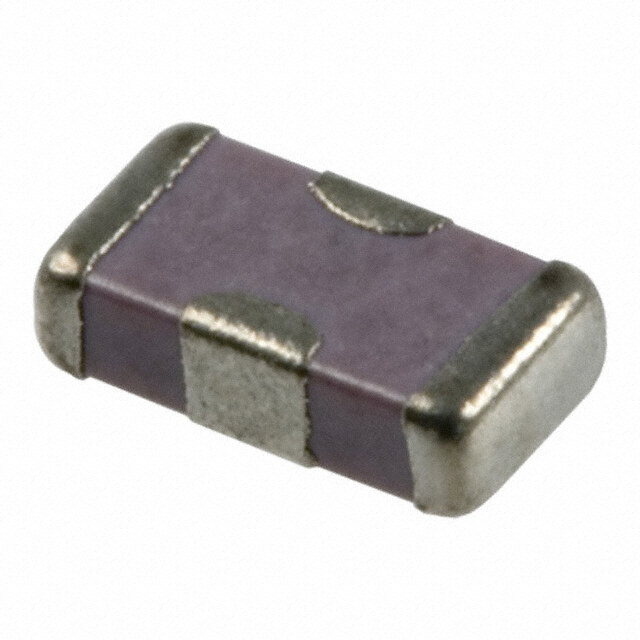
NFM18CC471R1C3D产品简介:
ICGOO电子元器件商城为您提供NFM18CC471R1C3D由Murata设计生产,在icgoo商城现货销售,并且可以通过原厂、代理商等渠道进行代购。 NFM18CC471R1C3D价格参考¥1.99-¥3.32。MurataNFM18CC471R1C3D封装/规格:馈通式电容器, 470pF Feed Through Capacitor 16V 500mA 300 mOhm 0603 (1608 Metric), 3 PC Pad。您可以下载NFM18CC471R1C3D参考资料、Datasheet数据手册功能说明书,资料中有NFM18CC471R1C3D 详细功能的应用电路图电压和使用方法及教程。
| 参数 | 数值 |
| 产品目录 | |
| DC电阻(DCR) | 300 毫欧最大 |
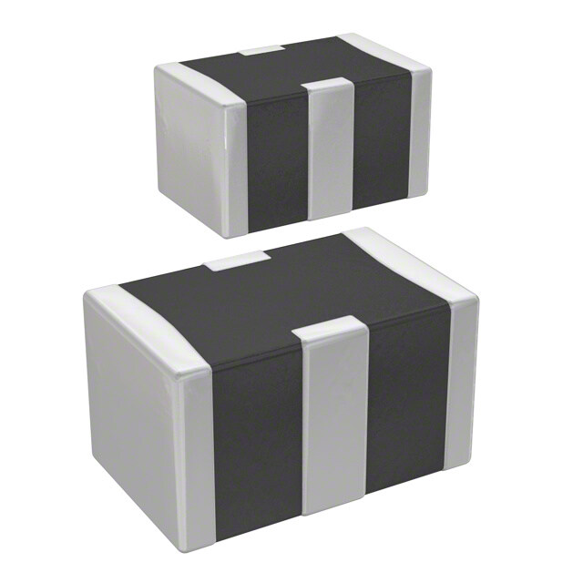
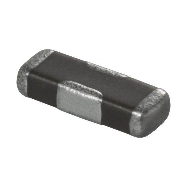
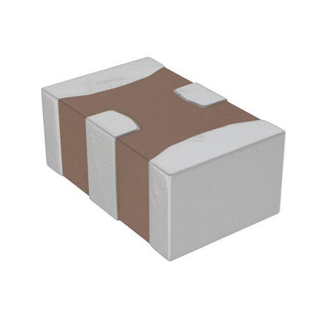
| 描述 | FILTER LC HIGH FREQ 470PF 0603馈通电容器 0603 470pF +/-20% 16 volt 500mA |
| 产品分类 | |
| 品牌 | Murata Electronics |
| 产品手册 | |
| 产品图片 |
|
| rohs | 符合RoHS无铅 / 符合限制有害物质指令(RoHS)规范要求 |
| 产品系列 | 馈通电容器,Murata Electronics NFM18CC471R1C3DEMIFIL®, NFM18C |
| 数据手册 | |
| 产品型号 | NFM18CC471R1C3D |
| 产品 | Three Terminal Filter Capacitors |
| 产品种类 | 馈通电容器 |
| 其它名称 | 490-6968-1 |
| 包装 | 剪切带 (CT) |
| 商标 | Murata Electronics |
| 外壳宽度 | 0.8 mm |
| 外壳长度 | 1.6 mm |
| 外壳高度 | 0.6 mm |
| 大小/尺寸 | 0.063" 长 x 0.031" 宽(1.60mm x 0.80mm) |
| 容差 | 20 % |
| 封装 | Reel |
| 封装/外壳 | 0603(1608 公制),3 PC 板 |
| 封装/箱体 | 0603 (1608 metric) |
| 工作温度 | -55°C ~ 125°C |
| 工厂包装数量 | 4000 |
| 接地端子 | 0.4 mm |
| 最大工作温度 | + 125 C |
| 最小工作温度 | - 55 C |
| 标准包装 | 1 |
| 电压 | 16V |
| 电压额定值DC | 16 V |
| 电容 | 470 pF |
| 电流 | 500mA |
| 电流额定值 | 300 mA |
| 端接类型 | SMD/SMT |
| 类型 | Three Terminal Capacitor |
| 系列 | NFM |
| 绝缘电阻 | 1000 MOhms |
| 螺纹尺寸 | - |
| 高度(最大值) | 0.028"(0.70mm) |

,-3-PC-Pad.jpg)


- 商务部:美国ITC正式对集成电路等产品启动337调查
- 曝三星4nm工艺存在良率问题 高通将骁龙8 Gen1或转产台积电
- 太阳诱电将投资9.5亿元在常州建新厂生产MLCC 预计2023年完工
- 英特尔发布欧洲新工厂建设计划 深化IDM 2.0 战略
- 台积电先进制程称霸业界 有大客户加持明年业绩稳了
- 达到5530亿美元!SIA预计今年全球半导体销售额将创下新高
- 英特尔拟将自动驾驶子公司Mobileye上市 估值或超500亿美元
- 三星加码芯片和SET,合并消费电子和移动部门,撤换高东真等 CEO
- 三星电子宣布重大人事变动 还合并消费电子和移动部门
- 海关总署:前11个月进口集成电路产品价值2.52万亿元 增长14.8%

PDF Datasheet 数据手册内容提取
3 Terminals Low ESL Chip Multilayer Ceramic Capacitors (EMIFIL) for General Purpose NFM18CC471R1C3_ (0603, 470pF, DC16V) _: packaging code Reference Sheet 1.Scope This product specification is applied to 3 Terminals Low ESL Chip Multilayer Ceramic Capacitorss (EMIFIL) used for General Electronic equipment. 2.MURATA Part NO. System (Ex.) NFM 18 CC 471 R 1C 3 D Dim(1e)Ln/sWions (2)Features C(3a)pNaocmitainnacle (4)Characteristics (5)DC Rated Voltage (6)Electrode (7)Packaging Code 3. Type & Dimensions a)Equivalent Circuit (Unit:mm) (1)-1 L (1)-2 W T e g i j 1.6±0.1 0.8±0.1 0.6±0.1 0.25±0.1 0.2 min. 0.4±0.1 0.2±0.1 4.Rated value (5) Rated (3) Nominal Capacitance DC Insulation Specifications and Test Methods DC Rated Current Capacitance Tolerance Resistance Resistance (Operating /Storage Temp. Range) Voltage (mA) 470 pF ±20 % DC 16 V 500mA(DC)300mΩmax.1000MΩmin. -55 to 125 °C / -55 to 125 °C 5.Package mark (7) Packaging Packaging Unit f180mm Reel D 4000 pcs./Reel PAPER W8P4 Product specifications in this catalog are as of Dec.7,2017,and are subject to change or obsolescence without notice. Please consult the approval sheet before ordering. Please read rating and !Cautions first. NFM18CC471R1C3-01 1
■SPECIFICATIONS AND TEST METHODS Electrical Performance No Item Specification Test Method 1 Capacitance Shown in Rated value. Frequency (Cap.) 22 to 47pF : 1±0.1MHz 100 to 22000pF : 1±0.1kHz Voltage : 1±0.2V(rms) 2 Insulation Voltage : Rated Voltage Resistance(I.R.) Time : 2 minutes max. 3 DC Resistance Measured with 100mA max. 4 Withstanding Voltage Products shall not be damaged. Test Voltage : Rated Voltage x 300% Time : 1 to 5 s Charge Current : 50mA max. 5 Operating Temperature Shown in Rated value. Includes self-heating 6 Storage Temperature Standard Testing Condition < Unless otherwise specified > < In case of doubt > Temperature : Ordinary Temp. / 15 °C to 35 °C Temperature: 20 °C ± 2 °C Humidity: Ordinary Humidity / 25 %(RH) to 85 %(RH) H u m i d i t y : 60 %(RH) to 70 %(RH) Atmospheric pressure: 86 kPa to 106 kPa JEMCPS-02209D 2
■SPECIFICATIONS AND TEST METHODS Mechanical Performance No Item Specification Test Method 1 Appearance and Appearance:No defects or abnormalities. Appearance:Visual inspection. Dimensions Dimensions:Within the specified dimensions. Dimensions:Using Measuring instrument of dimension. 2 Solderability Electrodes shall be at least 90% covered with Flux : Solution of rosin ethanol 25(mass)% new solder coating. Pre-heat : 150±10°C, 60 to 90s Solder : Sn-3.0Ag-0.5Cu Solder Temperature : 240±3°C Immersion Time : 3±1s Immersion and emersion rates : 25mm/s 3 Resistance to Meet Table 1. Flux : Solution of rosin ethanol 25(mass)% soldering heat Table 1 Pre-heat : 150±10°C, 60 to 90s Appearance No damaged Solder : Sn-3.0Ag-0.5Cu Cap. Change Within ±7.5% Solder Temperature : 270±5°C I.R. Meet the initial rated value. Immersion Time : 10±1s 22 to 2200pF 0.5max. Immersion and emersion rates : 25mm/s Rdc 22000pF 0.05max. Initial values : About 100 to 22000pF, measured after heat treatment (150+0/-10 °C,1hour) and exposure in the room condition for 48±4 hours. Then measured after exposure in the room condition for following hours. 22 to 47pF : 24±2 hours 100 to 22000pF : 48±4 hours 4 Bending Strength Meet Table 2. It shall be soldered on the glass-epoxy substrate(t=1.0mm). Table 2 Deflection : 2mm Appearance No damaged Keep ing Time : 30s Pressurejig Cap. Change Within ±7.5% 22 to 2200pF 0.5max. R340 F Rdc 22000pF 0.05max. Deflection 45 45 Product (in mm) 5 Drop Products shall be no failure after tested. It shall be dropped on concrete or steel board. Method : Free fall Height : 1m Attitude from which the product is dropped : 3 directions The Number of Time : 3 times for each direction (Total 9 times) 6 Bonding Strength The electrodes shall be no failure after tested. It shall be soldered on the glass-epoxy substrate. Applying Force (F) : 9.8N Applying Time : 30s 0.5 0.6 (in mm) 0.4 1.6 7 Vibration Meet Table 3. It shall be soldered on the glass-epoxy substrate. Table 3 Oscillation Frequency : 10 to 2000 to 10Hz for 20 minutes. Appearance No damaged Total amplitude 1.5 mm or Acceleration amplitude 196m/s2 Capacitance Meet the initial rated value. whichever is smaller. 22 to 2200pF 0.5max. Time : A period of 2 hours in each of 3 mutually Rdc 22000pF 0.05max. perpendicular directions. (Total 6 hours) Initial values : About 100 to 22000pF, measured after heat treatment (150+0/-10 °C,1hour) and exposure in the room condition for 48±4 hours. Then measured after exposure in the room condition for following hours. 22 to 47pF : 24±2 hours 100 to 22000pF : 48±4 hours JEMCPS-02209D 3
■SPECIFICATIONS AND TEST METHODS Environment Performance It shall be soldered on the glass-epoxy substrate. No Item Specification Test Method 1 Temperature Cycling Meet Table 1. 1 Cycle 1 step : -55+0/-3℃ / 30+3/-0 min 2 step : Room Temperature / within 3 min 3 step : +125+3/-0℃ / 30+3/-0 min 4 step : Room Temperature / within 3 min Total of 10 cycles Initial values : About 100 to 22000pF, measured after heat treatment(150+0/-10°C,1hour) and exposure in the room condition for 48±4 hours. Then measured after exposure in the room condition for following hours. 22 to 47pF : 24±2 hours 100 to 22000pF : 48±4 hours About 100 to 22000pF, If it’s doubt, measured after heat treatment (150+0/-10 °C,1hour) and exposure in the room condition for 48±4 hours. 2 Humidity Meet Table 4. Temperature : 40±2°C Table 4 Humidity : 90 to 95%(RH) Appearance No damaged Time : 500+24/-0 hours Appearance No damaged Cap. Change Within ±12.5% Initial values : About 100 to 22000pF,measured after heat Cap. Change Within ±12.5% treatment (150+0/-10 °C,1hour), and exposure in the room I.R. Meet the initial rated value. I.R. Meet the initial rated value. 22 to 2200pF 0.5max. condition for 48±4 hours. Rdc 1,2 22 to 2200pF 0.5 max. Rdc 22000pF 0.05max. Tfohlleonw imnge ahsouurresd. after exposure in the room condition for 22000pF 0.05 max. 22 to 47pF : 24±2 hours 100 to 22000pF : 48±4 hours About 100~22000pF, If it’s doubt, measured after heat treatment (150+0/-10 °C,1hour) and exposure in the room condition for 48±4 hours. 3 Heat Life Temperature : 125±2°C Test Voltage : Rated Voltage x 200% Charge Current : 50mA max. Time : 1000+48/-0 hours Initial values : About 100 to 22000pF,measured after voltage treatment (Maximum Operating Temperature±2°C, Rated Voltage x 200%, 1hour) and exposure in the room condition for 48±4 hours. Then measured after exposure in the room condition for following hours. 22 to 47pF : 24±2 hours 100 to 22000pF : 48±4 hours 4 Cold Resistance Temperature : -55±2°C Time : 500+24/-0 hours Initial values : About 100 to 22000pF,measured after heat treatment (150+0/-10 °C,1hour), and exposure in the room condition for 48±4 hours. Then measured after exposure in the room condition for following hours. 22 to 47pF : 24±2 hours 100 to 22000pF : 48±4 hours About 100 to 22000pF, If it’s doubt, measured after heat treatment (150+0/-10 °C,1hour) and exposure in the room condition for 48±4 hours. JEMCPS-02209D 4
P A C K A G I N G NFM18 Type 1. Appearance and D imensions (8mm-wide paper tape) 1 0. Sporocket Hole 4.0±0.1 f1.5±00.1 75± 1. Chip thickness Dimension 05 (T) (a) 0. 3 0.8 1.1max 5±0.1 3.5± 8.0±0. 0.6 0.9max 8 1. (in mm) 1.05±0.1 4.0±0.1 2.0±0.05 0.9maax. 2. Specification of Taping Direction of feed (1) Packing quantity (standard quantity) 4000 pcs. / reel (2) Packing Method Products shall be packaged in the cavity of the base tape and sealed by top tape and bottom tape. (3) Sprocket Hole The sprocket holes are to the right as the tape is pulled toward the user. (4) Base tape and Top tape The base tape and top tape have no spliced point. (5) Cavity There shall not be burr in the cavity. (6) Missing components number Missing components number within 0.1% of the number per reel or 1 pc., whichever is greater,and are not continuous. The specified quantity per reel is kept. 3. Pull Strength of Top Tape 5Nmin.(※Only for NFM18PS, 8Nmin.) 4. Peeling off force of top tape Toptape 0.1N to 0.6N (minimum value is typical)165to180degree F Speed of Peeling off : 300 mm / min Bottomtape Basetape 5. Dimensions of Leader-tape, Trailer and Reel There shall be leader-tape (top tape and empty tape) and trailer-tape (empty tape) as follows. Trailer Leader 2.0±0.5 160min. Label 190min. 210min. Emptytape Toptape f13.0±0.2 f60±10 f21.0±0.8 Directionoffeed 9±10 13±1.4 (in mm) f180±03 JEMCPP-02231A 5
! Caution ■Limitation of Applications Please contact us before using our products for the applications listed below which require especially high reliability for the prevention of defects which might directly cause damage to the third party's life, body or property. ①Aircraft equipment ②Aerospace equipment ③Undersea equipment ④Power plant control equipment ⑤Medical equipment ⑥Transportation equipment(vehicles,trains,ships,etc.) ⑦Traffic signal equipment ⑧Disaster prevention / crime prevention equipment ⑨Data-processing equipment ⑩Application of similar complexity and/or reliability requirements to the applications listed in the above. ■Storage and Operation condition 1. The performance of 3 Terminals Low ESL Chip Multilayer Ceramic Capacitors (EMIFIL) (henceforth just “capacitors”) may be affected by the storage conditions.Please use them promptly after delivery. 1-1. Maintain appropriate storage for the capacitors using the following conditions: Room Temperature of +5℃ to +40℃ and a Relative Humidity of 20% to 70%. High temperature and humidity conditions and/or prolonged storage may cause deterioration of the packaging materials. If more than six months have elapsed since delivery, check packaging, mounting, etc. before use. In addition, this may cause oxidation of the electrodes. If more than one year has elapsed since delivery, also check the solderability before use. 1-2. Corrosive gas can react with the termination (external) electrodes or lead wires of capacitors, and result in poor solderability. Do not store the capacitors in an atmosphere consisting of corrosive gas (e.g.,hydrogen sulfide, sulfur dioxide, chlorine, ammonia gas etc.). 1-3. Due to moisture condensation caused by rapid humidity changes, or the photochemical change caused by direct sunlight on the terminal electrodes and/or the resin/epoxy coatings, the solderability and electrical performance may deteriorate. Do not store capacitors under direct sunlight or in high huimidity conditions. ■Rating 1.Temperature Dependent Characteristics 1. The electrical characteristics of the capacitor can change with temperature. 1-1. For capacitors having larger temperature dependency, the capacitance may change with temperature changes. The following actions are recommended in order to ensure suitable capacitance values. (1) Select a suitable capacitance for the operating temperature range. (2) The capacitance may change within the rated temperature. When you use a high dielectric constant type capacitor in a circuit that needs a tight (narrow) capacitance tolerance (e.g., a time-constant circuit), please carefully consider the temperature characteristics, and carefully confirm the various characteristics in actual use conditions and the actual system. JEMCPC-05776B 6
! Caution 2.Measurement of Capacitance 1. Measure capacitance with the voltage and frequency specified in the product specifications. 1-1. The output voltage of the measuring equipment may decrease occasionally when capacitance is high. Please confirm whether a prescribed measured voltage is impressed to the capacitor. 1-2. The capacitance values of high dielectric constant type capacitors change depending on the AC voltage applied. Please consider the AC voltage characteristics when selecting a capacitor to be used in a AC circuit. 3.Applied Voltage , Applied Current 1. Do not apply a voltage to the capacitor that exceeds the rated voltage as called out in the specifications. 1-1. Applied voltage between the terminals of a capacitor shall be less than or equal to the rated voltage. (1) When AC voltage is superimposed on DC voltage, the zero-to-peak voltage shall not exceed the rated DC voltage. When AC voltage or pulse voltage is applied, the peak-to-peak voltage shall not exceed the rated DC voltage. (2) Abnormal voltages (surge voltage, static electricity, pulse voltage, etc.) shall not exceed the rated DC voltage. Typical Voltage Applied to the DC capacitor DC Voltage DC Voltage+AC AC Voltage Pulse Voltage E E E 0 E 0 0 0 (E:Maximum possible applied voltage.) 1-2. Influence of over voltage Over voltage that is applied to the capacitor may result in an electrical short circuit caused by the breakdown of the internal dielectric layers . The time duration until breakdown depends on the applied voltage and the ambient temperature. 2. The capacitors also have rated currents. The current flowing between the terminals of a capacitor (cid:10)shall be less than or equal to the rated current. Using the (cid:10)capacitor beyond this range could lead to excessive heat. 4.Type of Applied Voltage and Self-heating Temperature 1.Confirm the operating conditions to make sure that no large current is flowing into the capacitor due to the continuous application of an AC voltage or pulse voltage. When a DC rated voltage product is used in an AC voltage circuit or a pulse voltage circuit, the AC current or pulse current will flow into the capacitor; therefore check the self-heating condition. Please confirm the surface temperature of the capacitor so that the temperature remains within the upper limits of the operating temperature, including the rise in temperature due to self-heating. When the capacitor is used with a high-frequency voltage or pulse voltage, heat may be generated by dielectric loss. <Applicable to Rated Voltage of less than 100VDC> The load should be contained so that the self-heating of the capacitor body remains below 20°C , when(cid:10) measuring at an ambient temperature of 25°C. JEMCPC-05776B 7
! Caution 5. DC Voltage and AC Voltage Characteristic 1. The capacitance value of a high dielectric constant type capacitor changes depending on the DC voltage applied. Please consider the DC voltage characteristics when a capacitor is selected for use in a DC circuit. 1-1. The capacitance of ceramic capacitors may change sharply depending on the applied voltage. Please confirm the following in order to secure the capacitance. (1) Determine whether the capacitance change caused by the applied voltage is within the allowed range . (2) In the DC voltage characteristics, the rate of capacitance change becomes larger as voltage increases, even if the applied voltage is below the rated voltage. When a high dielectric constant type capacitor is used in a circuit that requires a tight (narrow) capacitance tolerance (e.g., a time constant circuit), please carefully consider the voltage characteristics, and confirm the various characteristics in the actual operating conditions of the system. 2. The capacitance values of high dielectric constant type capacitors changes depending on the AC voltage applied. Please consider the AC voltage characteristics when selecting a capacitor to be used in a AC circuit. 6. Capacitance Aging 1. The high dielectric constant type capacitors have an Aging characteristic in which the capacitance value decreases with the passage of time. When you use a high dielectric constant type capacitors in a circuit that needs a tight (narrow) capacitance tolerance (e.g., a time-constant circuit), please carefully consider the characteristics of these capacitors, such as their aging, voltage, and temperature characteristics. In addition, check capacitors using your actual appliances at the intended environment and operating conditions. 7.Vibration and Shock 1. Please confirm the kind of vibration and/or shock, its condition, and any generation of resonance. Please mount the capacitor so as not to generate resonance, and do not allow any impact on the terminals. 2. Mechanical shock due to being dropped may cause damage or a crack in the dielectric material of the capacitor. Do not use a dropped capacitor because the quality and reliability Crack may be deteriorated. Floor 3. When printed circuit boards are piled up or handled, the corner of another printed circuit board Mounting printed circuit board should not be allowed to hit the capacitor in order to avoid Crack a crack or other damage to the capacitor. JEMCPC-05776B 8
! Caution ■Soldering and Mounting 1.Mounting Position 1. Confirm the best mounting position and direction that minimizes the stress imposed on the capacitor during flexing or bending the printed circuit board. 1-1.Choose a mounting position that minimizes the stress imposed on the chip during flexing or bending of the board. [Component Direction] ① Locate chip horizontal to the direction in which stress acts. 1A (Bad Example) (Good Example) [Chip Mounting Close to Board Separation Point] It is effective to implement the following measures, to reduce stress in separating the board. It is best to implement all of the following three measures; however, implement as many measures as possible to reduce stress. Contents of Measures Stress Level (1) Turn the mounting direction of the component parallel to the board separation surface. A > D *1 (2) Add slits in the board separation part. A > B (3) Keep the mounting position of the component away from the board separation surface. A > C ① C Perforation B D 1A A Slit 1B ③ ② 1C *1 A > D is valid when stress is added vertically to the perforation as with Hand Separation. If a Cutting Disc is used, stress will be diagonal to the PCB, therefore A > D is invalid. [Mounting Capacitors Near Screw Holes] When a capacitor is mounted near a screw hole, it may be affected by the board deflection that occurs during the tightening of the screw. Mount the capacitor in a position as far away from the screw holes as possible. Recommended Screw Hole 2. If you mount the capacitor near components that (cid:10)generate heat, take note of the heat from the other (cid:10)components and carefully check the self-heating of the (cid:10)capacitor before using. If there is significant heat radiation from other (cid:10)components, it could lower the insulation resistance of (cid:10)the capacitor or produce excessive heat. JEMCPC-05776B 9
! Caution 2.Information before Mounting 1. Do not re-use capacitors that were removed from the equipment. 2. Confirm capacitance characteristics under actual applied voltage. 3. Confirm the mechanical stress under actual process and equipment use. 4. Confirm the rated capacitance, rated voltage and other electrical characteristics before assembly. 5. Prior to use, confirm the solderability of capacitors that were in long-term storage. 6. Prior to measuring capacitance, carry out a heat treatment for capacitors that were in long-term storage. 7.The use of Sn-Zn based solder will deteriorate the reliability of the MLCC. Please contact our sales representative or product engineers on the use of Sn-Zn based solder in advance. 3.Maintenance of the Mounting (pick and place) Machine 1. Make sure that the following excessive forces are not applied to the capacitors. Check the mounting in the actual device under actual use conditions ahead of time. 1-1. In mounting the capacitors on the printed circuit board, any bending force against them shall be kept to a minimum to prevent them from any damage or cracking. Please take into account the following precautions and recommendations for use in your process. (1) Adjust the lowest position of the pickup nozzle so as not to bend the printed circuit board. [Incorrect] Suction Nozzle Deflection Board Board Guide [Correct] Support Pin 2.Dirt particles and dust accumulated in the suction nozzle and suction mechanism prevent the nozzle from moving smoothly. This creates excessive force on the capacitor during mounting, causing cracked chips. Also, the locating claw, when worn out, imposes uneven forces on the chip when positioning, causing cracked chips. The suction nozzle and the locating claw must be maintained, checked and replaced periodically. JEMCPC-05776B 10
! Caution 4-1.Reflow Soldering 1. When sudden heat is applied to the components, the [Standard Conditions for Reflow Soldering] mechanical strength of the components will decrease because a sudden temperature change causes Temperature(℃) deformation inside the components. In order to prevent Peak Temperature Soldering mechanical damage to the components, preheating is 220℃ GCoraodliunagl required for both the components and the PCB. ΔT 190℃ Preheating conditions are shown in table 1. It is required to 170℃ keep the temperature differential between the solder and 150℃ Preheating the components surface (ΔT) as small as possible. 2. When components are immersed in solvent after mounting, Time 60-120 seconds 30-60 seconds be sure to maintain the temperature difference (ΔT) between the component and the solvent within the range shown in the table 1. [Allowable Reflow Soldering Temperature and Time] 280 Table 1 ℃) Series Chip Dimension(L/W) Code Temperature Differential erature( 227600 p NFM 15/JM/18/21/3D/31/41 ΔT≦190℃ Tem 250 ng 240 eri old 230 S 220 0 30 60 90 120 Soldering Time(s) In the case of repeated soldering, the accumulated Recommended Conditions soldering time must be within the range shown above. Lead Free Solder Peak Temperature 240 to 260℃ Atmosphere Air or N 2 Lead Free Solder: Sn-3.0Ag-0.5Cu 3. When a capacitor is mounted at a temperature lower than the peak reflow temperature recommended by the(cid:10) solder manufacturer, the following quality problems can occur. Consider factors such as the placement of(cid:10) peripheral components and the reflow temperature setting to prevent the capacitor’s reflow temperature from dropping below the peak temperature specified. Be sure to evaluate the mounting situation beforehand and(cid:10) verify that none of the following problems occur. ・Drop in solder wettability ・Solder voids ・Possible occurrence of whiskering ・Drop in bonding strength ・Drop in self-alignment properties ・Possible occurrence of tombstones and/or shifting on the land patterns of the circuit board 4. Optimum Solder Amount for Reflow Soldering 4-1. Overly thick application of solder paste results in a excessive solder fillet height. This makes the chip more susceptible to mechanical and thermal stress on the board and may cause the chips to crack. 4-2. Too little solder paste results in a lack of adhesive strength on the termination, which may result in chips breaking loose from the PCB. 4-3. Please confirm that solder has been applied smoothly to the termination. JEMCPC-05776B 11
! Caution [Guideline of solder paste thickness] 100 to 150μm : NFM15/JM/18/21/3D/31 100 to 200μm : NFM41 (in mm) NFM15CC/15PC NFMJMPC 0.3 0.95 0.5 0.9 1.4 NFM18CC/18PC NFM18PS NFM21CC/21PC NFM21PS NFM3DCC/3DPC NFM31PC/31KC NFM41CC/41PC Inverting the PCB Make sure not to impose any abnormal mechanical shocks to the PCB. JEMCPC-05776B 12
! Caution 4-2.Flow Soldering 1. Do not apply flow soldering to chips not listed in Table 2. [Standard Conditions for Flow Soldering] Table 2 Temperature(℃) Series Chip Dimension(L/W) Code Temperature Differential SPTeoemladkpe er irnagtu re Soldering Gradual ΔT Cooling NFM 3D/31/41 ΔT≦150℃ Preheating Peak Temperature Preheating Time 30-90 seconds 5 seconds max . 2. When sudden heat is applied to the components, the mechanical strength of the components will decrease because a sudden temperature change causes deformation inside the components. In order to prevent mechanical damage to the components, preheating is required for both of the components and the PCB. Preheating conditions are shown in table 2. It is required to [Allowable Flow Soldering Temperature and Time] keep the temperature differential between the solder and the components surface (ΔT) as low as possible. ℃) 280 e( 270 3. Excessively long soldering time or high soldering atur temperature can result in leaching of the terminations, per 260 m causing poor adhesion or a reduction in capacitance value g 250 n due to loss of contact between the inner electrodes and terminations. eri 240 d ol S 230 4. When components are immersed in solvent after mounting, 220 be sure to maintain the temperature differential (ΔT) 0 10 20 30 40 between the component and solvent within the range Soldering Time(s) shown in the table 2. In the case of repeated soldering, th e accumulated soldering time must be within the range shown above. Recommended Conditions Lead Free Solder Preheating Peak Temperature 140 to 160℃ Soldering Peak Temperature 250 to 260℃ Atmosphere Air or N 2 Lead Free Solder: Sn-3.0Ag-0.5Cu 5. Optimum Solder Amount for Flow Soldering Up to Chip Thickness 5-1. The top of the solder fillet should be lower than the thickness of the components. If the solder amount is excessive, the risk of cracking is higher during board bending or any other stressful condition. Adhesive in section JEMCPC-05776B 13
! Caution 4-3.Correction of Soldered Portion When sudden heat is applied to the capacitor, distortion caused by the large temperature difference occurs internally, and can be the cause of cracks. Capacitors also tend to be affected by mechanical and thermal stress depending on the board preheating temperature or the soldering fillet shape, and can be the cause of cracks. Please refer to "1. PCB Design" or "3. Optimum solder amount" for the solder amount and the fillet shapes. 1. Correction with a Soldering Iron 1-1. In order to reduce damage to the capacitor, be sure to preheat the capacitor and the mounting board. Preheat to the temperature range shown in Table 3. A hot plate, hot air type preheater, etc. can be used for preheating. 1-2. After soldering, do not allow the component/PCB to cool down rapidly. 1-3. Perform the corrections with a soldering iron as quickly as possible. If the soldering iron is applied too long, there is a possibility of causing solder leaching on the terminal electrodes, which will cause deterioration of the adhesive strength and other problems. Table 3 Chip Dimension Temperature of Preheating Temperature Series Atmosphere (L/W) Code Soldering Iron Tip Temperature Differential(ΔT) NFM 15 340℃ max. 150℃ min. ΔT≦190℃ Air NFM 18/21/3D/31/41 350℃ max. * Please do not rework with soldering iron for NFMJM series due to cracking concern. * Lead Free Solder: Sn-3.0Ag-0.5Cu * Please manage Δ T in the temperature of soldering iron and the preheating temperature. 2. Correction with Spot Heater Compared to local heating with a soldering iron, hot air heating by a spot heater heats the overall component and board, therefore, it tends to lessen the thermal shock. In the case of a high density mounted board, a spot heater can also prevent concerns of the soldering iron making direct contact with the component. 2-1. If the distance from the hot air outlet of the spot heater to the component is too close, cracks may occur due to thermal shock. To prevent this problem, follow the conditions shown in Table 4. 2-2. In order to create an appropriate solder fillet shape, it is recommended that hot air be applied at the angle shown in Figure 1. Table 4 Distance 5mm or more Hot Air Application angle 45° *Figure 1 Hot Air Temperature Nozzle Outlet 400°C max. Less than 10 seconds Application Time (3216M / 1206 size or smaller) Less than 30 seconds (4516M / 1806 size) (3216M , 4516M : Metric size code) [Figure 1] One-holeNozzle an Angle of 45° 3. Optimum solder amount when re-working with a soldering iron 3-1. If the solder amount is excessive, the risk of cracking is higher during board bending or any other stressful condition. Solder Amount Too little solder amount results in a lack of adhesive strength on the termination, which may result in chips breaking loose from the PCB. Please confirm that solder has been applied smoothly is in section and rising to the end surface of the chip. 3-2. A soldering iron with a tip of ø3mm or smaller should be used. It is also necessary to keep the soldering iron from touching the components during the re-work. 3-3. Solder wire with ø0.5mm or smaller is required for soldering. JEMCPC-05776B 14
! Caution 5.Washing Excessive ultrasonic oscillation during cleaning can cause the PCBs to resonate, resulting in cracked chips or broken solder joints. Before starting your production process, test your cleaning equipment / process to insure it does not degrade the capacitors. 6.Electrical Test on Printed Circuit Board 1. Confirm position of the support pin or specific jig, when inspecting the electrical performance of a capacitor after mounting on the printed circuit board. 1-1. Avoid bending the printed circuit board by the pressure of a test-probe, etc. The thrusting force of the test probe can flex the PCB, resulting in cracked chips or open solder joints. Provide support pins on the back side of the PCB to prevent warping or flexing. Install support pins as close to the test-probe as possible. 1-2. Avoid vibration of the board by shock when a test -probe contacts a printed circuit board. [Not Recommended] [Recommended] Peeling SupportPin Test-probe Test-probe 7.Printed Circuit Board Cropping 1. After mounting a capacitor on a printed circuit board, do not apply any stress to the capacitor that caused bending or twisting the board. 1-1. In cropping the board, the stress as shown may cause the capacitor to crack. Cracked capacitors may cause deterioration of the insulation resistance, and result in a short. Avoid this type of stress to a capacitor. ① [Bending] [Twisting] 1A 2. Check the cropping method for the printed circuit board in advance. 2-1. Printed circuit board cropping shall be carried out by using a jig or an apparatus (Disc separator, router type separator, etc.) to prevent the mechanical stress that can occur to the board. Hand Separation Board Separation Apparatus Board Separation Method (1) Board Separation Jig Nipper Separation 2) Disc Separator 3) Router Type Separator Level of stress on board High Medium Medium Low Recommended × △* △* ◯ · Board handling Hand and nipper · Board handling · Layout of slits separation apply a high · Board bending direction · Design of V groove Notes level of stress. Board handling · Layout of capacitors · Arrangement of blades Use another method. · Controlling blade life * When a board separation jig or disc separator is used, if the following precautions are not observed, a large board deflection stress will occur and the capacitors may crack. Use router type separator if at all possible. JEMCPC-05776B 15
! Caution (1) Example of a suitable jig [In the case of Single-side Mounting] An outline of the board separation jig is shown as follows. Recommended example: Stress on the component mounting position can be minimized by holding the portion close to the jig, and bend in the direction towards the side where the capacitors are mounted. Not recommended example: The risk of cracks occurring in the capacitors increases due to large stress being applied to the component mounting position, if the portion away from the jig is held and bent in the direction opposite the side where the capacitors are mounted. [Outline of jig] [Hand Separation] Recommended Not recommended Printed Circuit Board V-groove Pborianrtde d circuit Com ponDeirnetction of load L oad point Dl oiaredc tion of s Board Cropping Jig L oad point Pborianrtde d circuit C omponents [In the case of Double-sided Mounting] Since components are mounted on both sides of the board, the risk of cracks occurring can not be avoided with the above method. Therefore, implement the following measures to prevent stress from being applied to the components. (Measures) (1) Consider introducing a router type separator. If it is difficult to introduce a router type separator, implement the following measures. (Refer to item 1. Mounting Position) (2) Mount the components parallel to the board separation surface. (3) When mounting components near the board separation point, add slits in the separation position near the component. (4) Keep the mounting position of the components away from the board separation point. (2) Example of a Disc Separator An outline of a disc separator is shown as follows. As shown in the Principle of Operation, the top blade and bottom blade are aligned with the V-grooves on the printed circuit board to separate the board. In the following case, board deflection stress will be applied and cause cracks in the capacitors. (1) When the adjustment of the top and bottom blades are misaligned, such as deviating in the top-bottom, left-right or front-rear directions (2) The angle of the V groove is too low, depth of the V groove is too shallow, or the V groove is misaligned top-bottom IF V groove is too deep, it is possible to brake when you handle and carry it. Carefully design depth of the V groove with consideration about strength of material of the printed circuit board. [ Outline of Machine ] [ Principle of Operation ] [ Cross-section Diagram ] Top Blade Printed Circuit Board Top Blade V-groove Bottom Blade Printed Circuit Board V-groove [Disc Separator] Not recommended Recommended Top-bottom Misalignment Left-right Misalignment Front-rear Misalignment Top Blade Top Blade Top Blade Top Blade Bottom Blade Bottom Blade Bottom Blade Bottom Blade [V-groove Design] Example of Recommended Not Recommended V-groove Design Left-right Misalignment Low-Angle Depth too Shallow Depth too Deep JEMCPC-05776B 16
! Caution (3) Example of Router Type Separator The router type separator performs cutting by a router [Outline Drawing ] Router rotating at a high speed. Since the board does not bend in the cutting process, stress on the board can be suppressed during board separation. When attaching or removing boards to/from the router type separator, carefully handle the boards to prevent bending. 8. Assembly 1. Handling If a board mounted with capacitors is held with one hand, the board may bend. Firmly hold the edges of the board with both hands when handling. If a board mounted with capacitors is dropped, cracks may occur in the capacitors. Do not use dropped boards, as there is a possibility that the quality of the capacitors may be impaired. 2. Attachment of Other Components 2-1. Mounting of Other Components Pay attention to the following items, when mounting other components on the back side of the board after capacitors have been mounted on the opposite side. When the bottom dead point of the suction nozzle is set too low, board deflection stress may be applied to the capacitors on the back side (bottom side), and cracks may occur in the capacitors. · After the board is straightened, set the bottom dead point of the nozzle on the upper surface of the board. · Periodically check and adjust the bottom dead point. Suction Nozzle 2-2. Inserting Components with Leads into Boards When inserting components (transformers, IC, etc.) into boards, bending the board may cause cracks in the capacitors or cracks in the solder. Pay attention to the following. · Increase the size of the holes to insert the leads, to reduce the stress on the board during insertion. · Fix the board with support pins or a dedicated jig before insertion. · Support below the board so that the board does not bend. When using support pins on the board, periodically confirm that there is no difference in the height of each support pin. Componentwith Leads 2-3. Attaching/Removing Sockets and/or Connectors Insertion and removal of sockets and connectors,(cid:10)etc., might cause the board to bend. Please insure (cid:10)that the board does not warp during insertion and (cid:10)removal of sockets and connectors, etc., or the (cid:10)bending may damage mounted components on the (cid:10)board. Socket 2-4. Tightening Screws The board may be bent, when tightening screws, etc. during the attachment of the board to a shield or chassis. Pay attention to the following items before performing the work. · Plan the work to prevent the board from bending. · Use a torque screwdriver, to prevent over-tightening of the screws. · The board may bend after mounting by reflow soldering, etc. Please note, as stress may be applied to the chips by forcibly flattening the board when tightening the screws. Screwdriver JEMCPC-05776B 17
! Caution ■ Others 1. Under Operation of Equipment 1-1. Do not touch a capacitor directly with bare hands during operation in order to avoid the danger of an electric shock. 1-2. Do not allow the terminals of a capacitor to come in contact with any conductive objects (short-circuit). Do not expose a capacitor to a conductive liquid, inducing any acid or alkali solutions. 1-3. Confirm the environment in which the equipment will operate is under the specified conditions. Do not use the equipment under the following environments. (1) Being spattered with water or oil. (2) Being exposed to direct sunlight. (3) Being exposed to ozone, ultraviolet rays, or radiation. (4) Being exposed to toxic gas (e.g., hydrogen sulfide, sulfur dioxide, chlorine, ammonia gas etc.) (5) Any vibrations or mechanical shocks exceeding the specified limits. (6) Moisture condensing environments. 1-4. Use damp proof countermeasures if using under any conditions that can cause condensation. 2. Others 2-1. In an Emergency (1) If the equipment should generate smoke, fire, or smell, immediately turn off or unplug the equipment. If the equipment is not turned off or unplugged, the hazards may be worsened by supplying continuous power. (2) In this type of situation, do not allow face and hands to come in contact with the capacitor or burns may be caused by the capacitor's high temperature. 2-2. Disposal of waste When capacitors are disposed of, they must be burned or buried by an industrial waste vendor with the appropriate licenses. 2-3. Circuit Design (1) Addition of Fail Safe Function Capacitors that are cracked by dropping or bending of the board may cause deterioration of the insulation resistance, and result in a short. If the circuit being used may cause an electrical shock, smoke or fire when a capacitor is shorted, be sure to install fail-safe functions, such as a fuse, to prevent secondary accidents. (2) This series are not safety standard certified products. 2-4. Remarks Failure to follow the cautions may result, worst case, in a short circuit and smoking when the product is used. The above notices are for standard applications and conditions. Contact us when the products are used in special mounting conditions. Select optimum conditions for operation as they determine the reliability of the product after assembly. The data herein are given in typical values, not guaranteed ratings. JEMCPC-05776B 18
Notice ■ Rating 1.Operating Temperature 1. The operating temperature limit depends on the capacitor. 1-1. Do not apply temperatures exceeding the maximum operating temperature. It is necessary to select a capacitor with a suitable rated temperature that will cover the operating temperature range. It is also necessary to consider the temperature distribution in equipment and the seasonal temperature variable factor. 1-2. Consider the self-heating factor of the capacitor The surface temperature of the capacitor shall not exceed the maximum operating temperature including self-heating. 2.Atmosphere Surroundings (gaseous and liquid) 1. Restriction on the operating environment of capacitors. 1-1. Capacitors, when used in the above, unsuitable, operating environments may deteriorate due to the corrosion of the terminations and the penetration of moisture into the capacitor. 1-2. The same phenomenon as the above may occur when the electrodes or terminals of the capacitor are subject to moisture condensation. 1-3. The deterioration of characteristics and insulation resistance due to the oxidization or corrosion of terminal electrodes may result in breakdown when the capacitor is exposed to corrosive or volatile gases or solvents for long periods of time. 3.Piezo-electric Phenomenon 1. When using high dielectric constant type capacitors in AC or pulse circuits, the capacitor itself vibrates at specific frequencies and noise may be generated. Moreover, when the mechanical vibration or shock is added to capacitor, noise may occur. JEMCPC-05776B 19
Notice ■Soldering and Mounting 1.PCB Design 1. Notice for Pattern Forms 1-1. Unlike leaded components, chip components are susceptible to flexing stresses since they are mounted directly on the substrate. They are also more sensitive to mechanical and thermal stresses than leaded components. Excess solder fillet height can multiply these stresses and cause chip cracking. When designing substrates, take land patterns and dimensions into consideration to eliminate the possibility of excess solder fillet height. 1-2. There is a possibility of chip cracking caused by PCB expansion/contraction with heat, because stress(cid:10) (cid:10) (cid:10) on a chip is different depending on PCB material and structure.When the thermal expansion coefficient greatly differs between the board used for mounting and the chip,it will cause cracking of the chip due to the thermal expansion and contraction. When capacitors are mounted on a fluorine resin printed circuit board or on a single-layered glass epoxy board, it may also cause cracking of the chip for the same reason. 1-3. Because noise is suppressed by shunting unwanted high-frequency components to the ground, when designing a land for capacitor, design the ground pattern to be as large as possible in order to better bring out this characteristic. As shown in the figure below, noise countermeasures can be made more effective by using a via or etc. to connect the ground pattern on the chip mounting surface to a larger ground pattern on the inner layer. Pattern Forms Prohibited Correct Chassis Sol der (ground) Solder Resis t Placing Close to Chassis Electrode Pattern in section in section Lea d Wire So lder Resist PClaocminpgo onfe Cnhtsip and Leaded Components in section in section Soldering Iron Lead Wire Placing of Leaded Solder Res ist Components after Chip Component in section in section ソルダレジスト Solder R esist Lateral Mounting JEMCPC-05776B 20
Notice 2. Land Dimensions Please confirm the suitable land dimension by evaluating of the actual SET / PCB. (in mm) Series Land Dimensions ●Reflow Soldering NFM15CC/NFM15PC NFMJMPC Filled viaφ0.15 3 0. 0.3 0.95 0 0.25 0.5* In case of changing the land 0.9* dimentions marked by *, 1.4 a solder bridge between terminations of the chip could occur. In this case, please contact us before change. NFM18CC/NFM18PC NFM18PS NFM15CC NFM15PC NFMJMPC NFM18CC NFM18PC NFM18PS NFM21CC NFM21PC NFM21PS NFM21CC/NFM21PC NFM21PS JEMCPC-05776B 21
Notice (in mm) Series Land Dimensions ●Reflow Soldering Chip mounting side NFM3DCC/NFM3DPC/NFM31PC/NFM41CC/NFM41PC Dimensions Part Number a b c d e f g NFM3DCC 1.0 1.4 2.5 4.4 1.0 2.0 2.4 NFM3DPC NFM31PC 1.0 1.4 2.5 4.4 1.2 2.6 3.0 NFM41CC 1.5 2.0 3.5 6.0 1.2 2.6 3.0 NFM41PC NFM31KC *1 *1 For large current (cid:10)design, width of (cid:10)signal land pattern should be wider not less than 1mm per 1A (1mm/A). For example, in case of 10A, signal land pattern width should be 10mm or more. (1mm/A*10A=10mm) NFM3DCC NFM3DPC NFM31PC ●Flow Soldering Chip mounting side NFM31KC NFM41CC NFM3DCC/NFM3DPC/NFM31PC/NFM41CC/NFM41PC NFM41PC Dimensions Part Number a b c d e f g NFM3DCC 1.0 1.4 2.5 4.4 1.0 2.0 2.4 NFM3DPC NFM31PC 1.0 1.4 2.5 4.4 1.2 2.6 3.0 NFM41CC 1.5 2.0 3.5 6.0 1.2 2.6 3.0 NFM41PC NFM31KC *1 *1 For large current (cid:10)design, width of (cid:10)signal land pattern should be wider not less than 1mm per 1A (1mm/A). For example, in case of 10A, signal land pattern width should be 10mm or more. (1mm/A*10A=10mm) JEMCPC-05776B 22
Notice 3. Board Design Relationship with amount of strain to the board thickness, length, width, etc.] When designing the board, keep in mind that 3PL the amount of strain which occurs will increase ε= Relationship between load and strain depending on the sizeand material of the board. 2Ewh2 ε:Strain on center of board (μst) P Y Lw: :DBisotaanrdc ew bidetthw (ememn )s u pporting points (mm) h :Board thickness (mm) E :Elastic modulus of board (N/m2=Pa) h Y :Deflection (mm) P :Load (N) L w When the load is constant, the following relationship can be established. 2.Item to be confirmed for Flow sordering · As the distance between the supporting points (L) increases,the amount of strain also increases. →Reduce the distance between the supporting points. · As the elastic modulus (E) decreases, the amount of strain increases. If you want to temporarily attach the capacitor →Increase the elastic modulus. · As the board width (w) decreases, the amount of strain increases. to the board using an adhesive agent before →Increase the width of the board. · As the board thickness (h) decreases, the amount of strain increases. soldering the capacitor, first be sure that the →Increase the thickness of the board. Since the board thickness is squared, the effect on the amount of strain becomes even greater. conditions are appropriate for affixing the capacitor. If the dimensions of the land, the type of adhesive,the amount of coating, the contact surface area, the curing temperature, or other conditions are inappropriate, the characteristics of the capacitor may deteriorate. 1. Selection of Adhesive 1-1. Depending on the type of adhesive, there may be a decrease in insulation resistance. In addition, there is a chance that the capacitor might crack from contractile stress due to the difference in the contraction rate of the capacitor and the adhesive. 1-2. If there is not enough adhesive, the contact surface area is too small, or the curing temperature or curing time are inadequate, the adhesive strength will be insufficient and the capacitor may loosen or become disconnected during transportation or soldering. If there is too much adhesive, for example if it overflows onto the land, the result could be soldering defects, loss of electrical connection, insufficient curing, or slippage after the capacitor is mounted.(cid:10) Furthermore, if the curing temperature is too high or the curing time is too long, not only will the adhesive strength be reduced, but solderability may also suffer due to the effects of oxidation on the terminations (outer electrodes) of the capacitor and the land surface on the board. (1) Selection of Adhesive Epoxy resins are a typical class of adhesive. To select the proper adhesive, consider the following points. 1) There must be enough adhesive strength to prevent the component from loosening or slipping during the mounting process. 2) The adhesive strength must not decrease when exposed to moisture during soldering. 3) The adhesive must have good coatability and shape retention properties. 4) The adhesive must have a long pot life. 5) The curing time must be short. 6) The adhesive must not be corrosive to the exterior of the capacitor or the board. 7) The adhesive must have good insulation properties. 8) The adhesive must not emit toxic gases or otherwise be harmful to health. 9) The adhesive must be free of halogenated compounds. (2) Use the following illustration as a guide to the amount of adhesive to apply. Chip Dimension (L/W) Code:3D/31/41 JEMCPC-05776B 23
Notice 2.Flux 2-1. An excessive amount of flux generates a large quantity of flux gas, which can cause a deterioration of solderability, so apply flux thinly and evenly throughout. (A foaming system is generally used for flow solderring.) 2-2. Flux containing too high a percentage of halide may cause corrosion of the terminations unless there is sufficient cleaning. Use flux with a halide content of 0.1% max. 2-3. Strong acidic flux can corrode the capacitor and degrade its performance. Please check the quality of capacitor after mounting. 3.Leaching of the terminations Set temperature and time to ensure that leaching of the [As a Single Chip] terminations does not exceed 25% of the chip end area as a single chip (full length of the edge A-B-C-D A shown at right) and 25% of the length A-B shown as B mounted on substrate. D Termination C [As Mounted on Substrate] B A 3.Reflow soldering The flux in the solder paste contains halogen-based substances and organic acids as activators. Strong acidic flux can corrode the capacitor and degrade its performance. Please check the quality of capacitor after mounting. 4.Washing 1. Please evaluate the capacitor using actual cleaning equipment and conditions to confirm the quality, and select the solvent for cleaning. 2. Unsuitable cleaning may leave residual flux or other foreign substances, causing deterioration of electrical characteristics and the reliability of the capacitors. 5.Coating 1. A crack may be caused in the capacitor due to the stress of the thermal contraction of the resin during curing process. The stress is affected by the amount of resin and curing contraction. Select a resin with low curing contraction. The difference in the thermal expansion coefficient between a coating resin or a molding resin and the capacitor may cause the destruction and deterioration of the capacitor such as a crack or peeling, and lead to the deterioration of insulation resistance or dielectric breakdown. Select a resin for which the thermal expansion coefficient is as close to that of the capacitor as possible. A silicone resin can be used as an under-coating to buffer against the stress. 2. Select a resin that is less hygroscopic. Using hygroscopic resins under high humidity conditions may cause the deterioration of the insulation resistance of a capacitor. An epoxy resin can be used as a less hygroscopic resin. 3.The halogen system substance and organic acid are included in coating material, and a chip corrodes by the kind of Coating material. Do not use strong acid type. JEMCPC-05776B 24
Notice ■ Others 1.Transportation 1. The performance of a capacitor may be affected by the conditions during transportation. 1-1. The capacitors shall be protected against excessive temperature, humidity and mechanical force during transportation. (1) Climatic condition ・ low air temperature : -40℃ ・ change of temperature air/air : -25℃/+25℃ ・ low air pressure : 30 kPa ・ change of air pressure : 6 kPa/min. (2) Mechanical condition Transportation shall be done in such a way that the boxes are not deformed and forces are not directly passed on to the inner packaging. 1-2. Do not apply excessive vibration, shock, or pressure to the capacitor. (1) When excessive mechanical shock or pressure is applied to a capacitor, chipping or cracking may occur in the ceramic body of the capacitor. (2) When the sharp edge of an air driver, a soldering iron, tweezers, a chassis, etc. impacts strongly on the surface of the capacitor, the capacitor may crack and short-circuit. 1-3. Do not use a capacitor to which excessive shock was applied by dropping etc. A capacitor dropped accidentally during processing may be damaged. 2.Characteristics Evaluation in the Actual System 1. Evaluate the capacitor in the actual system,to confirm that there is no problem with the performance and specification values in a finished product before using. 2. Since a voltage dependency and temperature dependency exists in the capacitance of high dielectric type ceramic capacitors, the capacitance may change depending on the operating conditions in the actual system. Therefore,be sure to evaluate the various characteristics, such as the leakage current and noise absorptivity, which will affect the capacitance value of the capacitor. 3. In addition,voltages exceeding the predetermined surge may be applied to the capacitor by the inductance in the actual system. Evaluate the surge resistance in the actual system as required. 4. The effects of noise suppression can vary depending on the usage conditions, including differences in the circuit or IC to be used, the type of noise, the shape of the pattern to be mounted, and the mounting location. Be sure to verify the effect on the actual device in advance. JEMCPC-05776B 25
! NOTE 1.Please make sure that your product has been evaluated in view of your specifications with our product being mounted to your product. 2.Your are requested not to use our product deviating from this product specification. 3.We consider it not appropriate to include any terms and conditions with regard to the business transaction in the product specifications, drawings or other technical documents. Therefore, if your technical documents as above include such terms and conditions such as warranty clause, product liability clause, or intellectual property infringement liability clause, they will be deemed to be invalid. JEMCPC-05776B 26