ICGOO在线商城 > 分立半导体产品 > 二极管 - 整流器 - 阵列 > VS-40L15CTPBF
 Datasheet下载
- 型号: VS-40L15CTPBF
- 制造商: Vishay
- 库位|库存: xxxx|xxxx
- 要求:
| 数量阶梯 | 香港交货 | 国内含税 |
| +xxxx | $xxxx | ¥xxxx |
查看当月历史价格
查看今年历史价格
VS-40L15CTPBF产品简介:
ICGOO电子元器件商城为您提供VS-40L15CTPBF由Vishay设计生产,在icgoo商城现货销售,并且可以通过原厂、代理商等渠道进行代购。 VS-40L15CTPBF价格参考¥13.00-¥16.25。VishayVS-40L15CTPBF封装/规格:二极管 - 整流器 - 阵列, Diode Array 1 Pair Common Cathode Schottky 15V 20A Through Hole TO-220-3。您可以下载VS-40L15CTPBF参考资料、Datasheet数据手册功能说明书,资料中有VS-40L15CTPBF 详细功能的应用电路图电压和使用方法及教程。
| 参数 | 数值 |
| 产品目录 | |
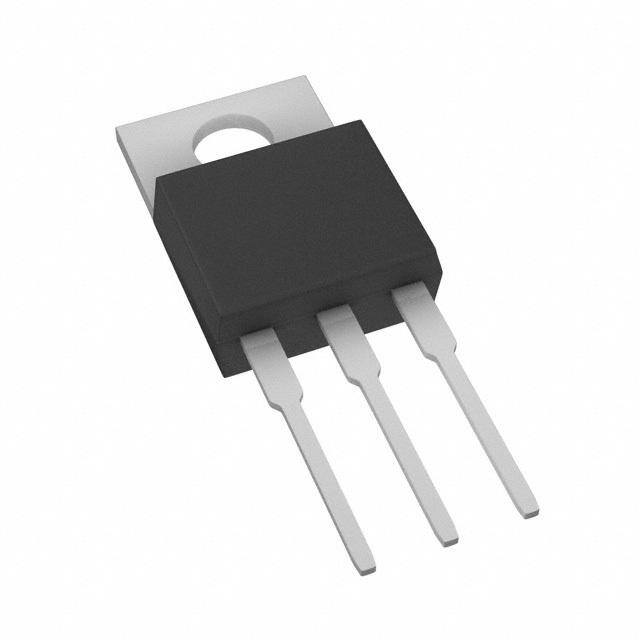
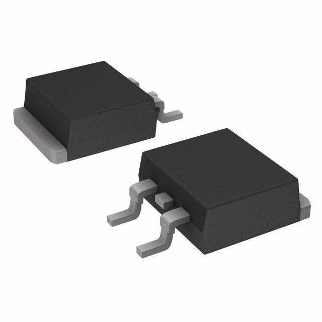
| 描述 | DIODE SCHOTTKY 15V 20A TO220AB肖特基二极管与整流器 40 Amp 15 Volt Common Cathode |
| 产品分类 | 二极管,整流器 - 阵列分离式半导体 |
| 品牌 | VishayVishay Semiconductor Diodes Division |
| 产品手册 | |
| 产品图片 |
|
| rohs | 符合RoHS无铅 / 符合限制有害物质指令(RoHS)规范要求 |
| 产品系列 | 二极管与整流器,肖特基二极管与整流器,Vishay VS-40L15CTPBF- |
| 数据手册 | |
| 产品型号 | VS-40L15CTPBFVS-40L15CTPBF |
| 不同If时的电压-正向(Vf) | 410mV @ 19A |
| 不同 Vr时的电流-反向漏电流 | 10mA @ 15V |
| 二极管类型 | |
| 二极管配置 | 1 对共阴极 |
| 产品 | Schottky Rectifiers |
| 产品目录绘图 |
|
| 产品目录页面 | |
| 产品种类 | 肖特基二极管与整流器 |
| 供应商器件封装 | TO-220AB |
| 其它名称 | *40L15CTPBF |
| 包装 | 管件 |
| 反向恢复时间(trr) | - |
| 商标 | Vishay |
| 安装类型 | 通孔 |
| 安装风格 | Through Hole |
| 封装 | Tube |
| 封装/外壳 | TO-220-3 |
| 封装/箱体 | TO-220-3 |
| 峰值反向电压 | 15 V |
| 工作温度范围 | - 55 C to + 125 C |
| 工厂包装数量 | 1000 |
| 技术 | Silicon |
| 最大反向漏泄电流 | 10 mA |
| 最大工作温度 | + 125 C |
| 最大浪涌电流 | 700 A |
| 最小工作温度 | - 55 C |
| 标准包装 | 50 |
| 正向电压下降 | 0.52 V at 40 A |
| 正向连续电流 | 20 A |
| 热阻 | 0.5°C/W Cs |
| 电压-DC反向(Vr)(最大值) | 15V |
| 电流-平均整流(Io)(每二极管) | 20A |
| 速度 | 快速恢复 =< 500 ns,> 200mA(Io) |
| 配置 | Dual Common Cathode |


- 商务部:美国ITC正式对集成电路等产品启动337调查
- 曝三星4nm工艺存在良率问题 高通将骁龙8 Gen1或转产台积电
- 太阳诱电将投资9.5亿元在常州建新厂生产MLCC 预计2023年完工
- 英特尔发布欧洲新工厂建设计划 深化IDM 2.0 战略
- 台积电先进制程称霸业界 有大客户加持明年业绩稳了
- 达到5530亿美元!SIA预计今年全球半导体销售额将创下新高
- 英特尔拟将自动驾驶子公司Mobileye上市 估值或超500亿美元
- 三星加码芯片和SET,合并消费电子和移动部门,撤换高东真等 CEO
- 三星电子宣布重大人事变动 还合并消费电子和移动部门
- 海关总署:前11个月进口集成电路产品价值2.52万亿元 增长14.8%


PDF Datasheet 数据手册内容提取
VS-40L15CTPbF, VS-40L15CT-N3 www.vishay.com Vishay Semiconductors Schottky Rectifier, 2 x 20 A FEATURES Base 2 common • 125 °C T operation (V < 5 V) J R cathode • Very low forward voltage drop • High frequency operation • High purity, high temperature epoxy encapsulation for enhanced mechanical strength Anode 2 Anode and moisture resistance TO-220AB 1 Common 3 cathode • Guard ring for enhanced ruggedness and long term reliability • Compliant to RoHS Directive 2002/95/EC PRODUCT SUMMARY • Designed and qualified according to JEDEC-JESD47 Package TO-220AB • Halogen-free according to IEC 61249-2-21 definition I 2 x 20 A (-N3 only) F(AV) V 15 V R DESCRIPTION V at I See Electrical table F F This center tap Schottky rectifier has been optimized for I max. 600 mA at 100 °C RM very low forward voltage drop, with moderate leakage. The T max. 125 °C proprietary barrier technology allows for reliable operation J up to 125 °C junction temperature. Typical applications are Diode variation Common cathode in switching power supplies, converters, freewheeling EAS 10 mJ diodes, and reverse battery protection. MAJOR RATINGS AND CHARACTERISTICS SYMBOL CHARACTERISTICS VALUES UNITS IF(AV) Rectangular waveform 40 A V 15 V RRM I t = 5 μs sine 700 A FSM p V 19 A , T = 125 °C (per leg) 0.25 V F pk J TJ Range - 55 to 125 °C VOLTAGE RATINGS PARAMETER SYMBOL VS-40L15CTPbF VS-40L15CT-N3 UNITS Maximum DC reverse voltage V R 15 15 V Maximum working peak reverse voltage V RWM ABSOLUTE MAXIMUM RATINGS PARAMETER SYMBOL TEST CONDITIONS VALUES UNITS Maximum average per leg 20 forward current IF(AV) 50 % duty cycle at TC = 85 °C, rectangular waveform See fig. 5 per device 40 A Maximum peak one cycle non-repetitive 5 μs sine or 3 μs rect. pulse Following any rated 700 surge current per leg IFSM load condition and with See fig. 7 10 ms sine or 6 ms rect. pulse rated VRRM applied 330 Non-repetitive avalanche energy per leg EAS TJ = 25 °C, IAS = 2 A, L = 6 mH 10 mJ Current decaying linearly to zero in 1 μs Repetitive avalanche current per leg IAR Frequency limited by T maximum V = 1.5 x V typical 2 A J A R Revision: 29-Aug-11 1 Document Number: 94216 For technical questions within your region: DiodesAmericas@vishay.com, DiodesAsia@vishay.com, DiodesEurope@vishay.com THIS DOCUMENT IS SUBJECT TO CHANGE WITHOUT NOTICE. THE PRODUCTS DESCRIBED HEREIN AND THIS DOCUMENT ARE SUBJECT TO SPECIFIC DISCLAIMERS, SET FORTH AT www.vishay.com/doc?91000
VS-40L15CTPbF, VS-40L15CT-N3 www.vishay.com Vishay Semiconductors ELECTRICAL SPECIFICATIONS PARAMETER SYMBOL TEST CONDITIONS TYP. MAX. UNITS 19 A - 0.41 T = 25 °C J Forward voltage drop per leg 40 A - 0.52 V (1) V See fig. 1 FM 19 A 0.25 0.33 T = 125 °C J 40 A 0.37 0.50 Reverse leakage current per leg TJ = 25 °C - 10 I (1) V = Rated V mA See fig. 2 RM T = 100 °C R R - 600 J Threshold voltage VF(TO) 0.182 V T = T maximum J J Forward slope resistance rt 7.6 m(cid:58) Maximum junction capacitance per leg CT VR = 5 VDC (test signal range 100 kHz to 1 MHz) 25 °C - 2000 pF Typical series inductance per leg LS Measured lead to lead 5 mm from package body 8 - nH Maximum voltage rate of change dV/dt Rated VR 10 000 V/μs Note (1) Pulse width < 300 μs, duty cycle < 2 % THERMAL - MECHANICAL SPECIFICATIONS PARAMETER SYMBOL TEST CONDITIONS VALUES UNITS Maximum junction and storage T , T - 55 to 125 °C temperature range J Stg Maximum thermal resistance, junction to case per leg RthJC DC operation 1.5 °C/W Typical thermal resistance, case to heatsink RthCS Mounting surface, smooth and greased 0.50 2 g Approximate weight 0.07 oz. minimum 6 (5) kgf · cm Mounting torque maximum 12 (10) (lbf · in) Marking device Case style TO-220AB 40L15CT Revision: 29-Aug-11 2 Document Number: 94216 For technical questions within your region: DiodesAmericas@vishay.com, DiodesAsia@vishay.com, DiodesEurope@vishay.com THIS DOCUMENT IS SUBJECT TO CHANGE WITHOUT NOTICE. THE PRODUCTS DESCRIBED HEREIN AND THIS DOCUMENT ARE SUBJECT TO SPECIFIC DISCLAIMERS, SET FORTH AT www.vishay.com/doc?91000
VS-40L15CTPbF, VS-40L15CT-N3 www.vishay.com Vishay Semiconductors A) 1000 1000 nt ( re A) TJ = 100 °C d Cur 100 nt (m 100 TJ = 75 °C r e a r w ur s For TJ = 125 °C se C 10 TJ = 50 °C ntaneou 10 TTJJ == 7255 °°CC - ReverR 1 TJ = 25 °C a I st n I - IF 10 0.2 0.4 0.6 0.8 1.0 1.2 1.4 1.6 0.10 3 6 9 12 15 V - Forward Voltage Drop (V) V - Reverse Voltage (V) FM R Fig. 1 - Maximum Forward Voltage Drop Characteristics Fig. 2 - Typical Values of Reverse Current vs. (Per Leg) Reverse Voltage (Per Leg) 10 000 F) p e ( c n a acit TJ = 25 °C p a 1000 C n o cti n u J - T C 100 0 5 10 15 20 V - Reverse Voltage (V) R Fig. 3 - Typical Junction Capacitance vs. Reverse Voltage (Per Leg) 10 W) C/ ° e ( c n a 1 d e p m D = 0.75 PDM al I D = 0.50 t m D = 0.33 1 her 0.1 DD == 00..2250 t2 T Notes: - C (theSrminagl lere psuisltsaence) 1. Duty factor D = t1/t2 ZthJ 2. Peak TJ = PDM x ZthJC + TC 0.01 0.00001 0.0001 0.001 0.01 0.1 1 10 100 t - Rectangular Pulse Duration (s) 1 Fig. 4 - Maximum Thermal Impedance Z Characteristics (Per Leg) thJC Revision: 29-Aug-11 3 Document Number: 94216 For technical questions within your region: DiodesAmericas@vishay.com, DiodesAsia@vishay.com, DiodesEurope@vishay.com THIS DOCUMENT IS SUBJECT TO CHANGE WITHOUT NOTICE. THE PRODUCTS DESCRIBED HEREIN AND THIS DOCUMENT ARE SUBJECT TO SPECIFIC DISCLAIMERS, SET FORTH AT www.vishay.com/doc?91000
VS-40L15CTPbF, VS-40L15CT-N3 www.vishay.com Vishay Semiconductors 100 14 C) D = 0.20 ° ature ( 95 s (W) 1102 DDD === 000...235530 emper 90 Square wave (D = 0.50) er Los 8 D = 0.75 RMS limit T 85 w se Po 6 Ca 80 ge e a 4 bl er a v DC w 75 A Allo See note (1) 2 70 0 0 4 8 12 16 20 24 0 5 10 15 20 25 30 I - Average Forward Current (A) I - Average Forward Current (A) F(AV) F(AV) Fig. 5 - Maximum Allowable Case Temperature vs. Fig. 6 - Forward Power Loss Characteristics (Per Leg) Average Forward Current (Per Leg) A) 1000 nt ( e r r u C e g r u S e v etiti Aant da nwyi trha treadte ldo aVd co nadpiptioliend p RRM e following surge R n- o N - M 100 S F 10 100 1000 10 000 I t - Square Wave Pulse Duration (μs) p Fig. 7 - Maximum Non-Repetitive Surge Current (Per Leg) L High-speed IRFP460 switch D.U.T. Rg = 25 Ω Fredeiowdheeel + Vd = 25 V Current monitor 40HFL40S02 Fig. 8 - Unclamped Inductive Test Circuit Note (1) Formula used: T = T - (Pd + Pd ) x R ; C J REV thJC Pd = Forward power loss = I x V at (I /D) (see fig. 6); F(AV) FM F(AV) Pd = Inverse power loss = V x I (1 - D); I at V = 10 V REV R1 R R R1 Revision: 29-Aug-11 4 Document Number: 94216 For technical questions within your region: DiodesAmericas@vishay.com, DiodesAsia@vishay.com, DiodesEurope@vishay.com THIS DOCUMENT IS SUBJECT TO CHANGE WITHOUT NOTICE. THE PRODUCTS DESCRIBED HEREIN AND THIS DOCUMENT ARE SUBJECT TO SPECIFIC DISCLAIMERS, SET FORTH AT www.vishay.com/doc?91000
VS-40L15CTPbF, VS-40L15CT-N3 www.vishay.com Vishay Semiconductors ORDERING INFORMATION TABLE Device code VS- 40 L 15 C T PbF 1 2 3 4 5 6 7 1 - Vishay Semiconductors product 2 - Current rating (40 = 40 A) 3 - Schottky “L” series 4 - Voltage rating (15 = 15 V) 5 - C = Common cathode 6 - Package: T = TO-220 7 - Environmental digit PbF = Lead (Pb)-free and RoHS compliant -N3 = Halogen-free, RoHS compliant, and totally lead (Pb)-free ORDERING INFORMATION (Example) PREFERRED P/N QUANTITY PER T/R MINIMUM ORDER QUANTITY PACKAGING DESCRIPTION VS-40L15CTPbF 50 1000 Antistatic plastic tube VS-40L15CT-N3 50 1000 Antistatic plastic tube LINKS TO RELATED DOCUMENTS Dimensions www.vishay.com/doc?95222 TO-220AB PbF www.vishay.com/doc?95225 Part marking information TO-220AB -N3 www.vishay.com/doc?95028 Revision: 29-Aug-11 5 Document Number: 94216 For technical questions within your region: DiodesAmericas@vishay.com, DiodesAsia@vishay.com, DiodesEurope@vishay.com THIS DOCUMENT IS SUBJECT TO CHANGE WITHOUT NOTICE. THE PRODUCTS DESCRIBED HEREIN AND THIS DOCUMENT ARE SUBJECT TO SPECIFIC DISCLAIMERS, SET FORTH AT www.vishay.com/doc?91000
Outline Dimensions Vishay Semiconductors TO-220AB DIMENSIONS in millimeters and inches B (6) A Seating E plane Thermal pad Ø P A A E2 (7) 0.014MBAM (E) A1 Q 1 2 3 (6) (H1) D D H1 L1 (2) (7) C C D2 (6) (6) D Detail B D1 3 x b 3 x b2 1 2 3 Detail B C E1 (6) L Base metal (b, b2) Plating View A - A c c1 (4) c A 2 x e A2 (4) e1 b1, b3 0.015MBAM Section C - C and D - D Lead assignments Lead tip Diodes Conforms to JEDEC outline TO-220AB 1. - Anode/open 2. - Cathode 3. - Anode MILLIMETERS INCHES MILLIMETERS INCHES SYMBOL NOTES SYMBOL NOTES MIN. MAX. MIN. MAX. MIN. MAX. MIN. MAX. A 4.25 4.65 0.167 0.183 E 10.11 10.51 0.398 0.414 3, 6 A1 1.14 1.40 0.045 0.055 E1 6.86 8.89 0.270 0.350 6 A2 2.56 2.92 0.101 0.115 E2 - 0.76 - 0.030 7 b 0.69 1.01 0.027 0.040 e 2.41 2.67 0.095 0.105 b1 0.38 0.97 0.015 0.038 4 e1 4.88 5.28 0.192 0.208 b2 1.20 1.73 0.047 0.068 H1 6.09 6.48 0.240 0.255 6, 7 b3 1.14 1.73 0.045 0.068 4 L 13.52 14.02 0.532 0.552 c 0.36 0.61 0.014 0.024 L1 3.32 3.82 0.131 0.150 2 c1 0.36 0.56 0.014 0.022 4 Ø P 3.54 3.73 0.139 0.147 D 14.85 15.25 0.585 0.600 3 Q 2.60 3.00 0.102 0.118 D1 8.38 9.02 0.330 0.355 (cid:84) 90° to 93° 90° to 93° D2 11.68 12.88 0.460 0.507 6 Notes (1) Dimensioning and tolerancing as per ASME Y14.5M-1994 (7) Dimensions E2 x H1 define a zone where stamping and (2) Lead dimension and finish uncontrolled in L1 singulation irregularities are allowed (3) Dimension D, D1 and E do not include mold flash. Mold flash (8) Outline conforms to JEDEC TO-220, except A2 (maximum) and shall not exceed 0.127 mm (0.005") per side. These dimensions D2 (minimum) where dimensions are derived from the actual are measured at the outermost extremes of the plastic body package outline (4) Dimension b1, b3 and c1 apply to base metal only (5) Controlling dimensions: inches (6) Thermal pad contour optional within dimensions E, H1, D2 and E1 Document Number: 95222 For technical questions within your region, please contact one of the following: www.vishay.com Revision: 08-Mar-11 DiodesAmericas@vishay.com, DiodesAsia@vishay.com, DiodesEurope@vishay.com 1
Legal Disclaimer Notice www.vishay.com Vishay Disclaimer (cid:3) ALL PRODUCT, PRODUCT SPECIFICATIONS AND DATA ARE SUBJECT TO CHANGE WITHOUT NOTICE TO IMPROVE RELIABILITY, FUNCTION OR DESIGN OR OTHERWISE. Vishay Intertechnology, Inc., its affiliates, agents, and employees, and all persons acting on its or their behalf (collectively, “Vishay”), disclaim any and all liability for any errors, inaccuracies or incompleteness contained in any datasheet or in any other disclosure relating to any product. Vishay makes no warranty, representation or guarantee regarding the suitability of the products for any particular purpose or the continuing production of any product. To the maximum extent permitted by applicable law, Vishay disclaims (i) any and all liability arising out of the application or use of any product, (ii) any and all liability, including without limitation special, consequential or incidental damages, and (iii) any and all implied warranties, including warranties of fitness for particular purpose, non-infringement and merchantability. Statements regarding the suitability of products for certain types of applications are based on Vishay’s knowledge of typical requirements that are often placed on Vishay products in generic applications. Such statements are not binding statements about the suitability of products for a particular application. It is the customer’s responsibility to validate that a particular product with the properties described in the product specification is suitable for use in a particular application. Parameters provided in datasheets and / or specifications may vary in different applications and performance may vary over time. All operating parameters, including typical parameters, must be validated for each customer application by the customer’s technical experts. Product specifications do not expand or otherwise modify Vishay’s terms and conditions of purchase, including but not limited to the warranty expressed therein. Except as expressly indicated in writing, Vishay products are not designed for use in medical, life-saving, or life-sustaining applications or for any other application in which the failure of the Vishay product could result in personal injury or death. Customers using or selling Vishay products not expressly indicated for use in such applications do so at their own risk. Please contact authorized Vishay personnel to obtain written terms and conditions regarding products designed for such applications. No license, express or implied, by estoppel or otherwise, to any intellectual property rights is granted by this document or by any conduct of Vishay. Product names and markings noted herein may be trademarks of their respective owners. © 2017 VISHAY INTERTECHNOLOGY, INC. ALL RIGHTS RESERVED Revision: 08-Feb-17 1 Document Number: 91000