首页 > HMC641LP4E > 详情
 Datasheet下载
- 型号: HMC641LP4E
- 制造商: Hittite
- 库位|库存: xxxx|xxxx
- 要求:
| 数量阶梯 | 香港交货 | 国内含税 |
| +xxxx | $xxxx | ¥xxxx |
查看当月历史价格
查看今年历史价格
产品参数
| 参数 | 数值 |
| 产品目录 | 射频/IF 和 RFID |
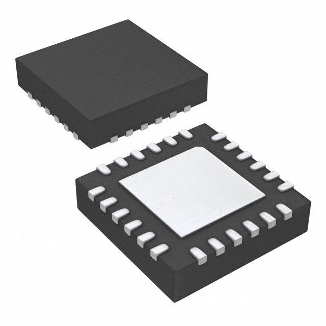
| 描述 | IC SWITCH SP4T NON-REFL 24-QFN |
| 产品分类 | RF 开关 |
| IIP3 | 38dBm (标准) |
| 品牌 | Hittite Microwave Corporation |
| 数据手册 | 点击此处下载产品Datasheet |
| 产品图片 |  |
| P1dB | 22dBm |
| 产品型号 | HMC641LP4E |
| RF类型 | 通用 |
| rohs | 无铅 / 符合限制有害物质指令(RoHS)规范要求 |
| 产品系列 | - |
| 供应商器件封装 | 24-TQFN(4x4) |
| 其它名称 | 1127-1502 1127-1502-1 1127-1502-ND |
| 包装 | 剪切带 (CT) |
| 封装/外壳 | 24-TQFN 裸露焊盘 |
| 工作温度 | -40°C ~ 85°C |
| 拓扑 | 吸收性 |
| 插损@频率 | 3dB @ 20GHz |
| 标准包装 | 1 |
| 特性 | - |
| 电压-电源 | - |
| 电路 | SP4T |
| 阻抗 | 50 欧姆 |
| 隔离@频率 | 40dB @ 20GHz (标准) |
| 频率 -上 | 20GHz |
| 频率 -下 | DC |
Datasheet
PDF Datasheet 数据手册内容提取
HMC641LP4E v02.0611 GaAs MMIC SP4T NoN-RefleCTIve SwITCh, DC - 20 Ghz Typical Applications features the hMc641LP4e is ideal for: Broadband Performance: Dc - 20 Ghz t • Telecom Infrastructure high isolation: 45 dB @ 10 Ghz M • Microwave Radio & VSAT Low insertion Loss: 2.3 dB @ 10 Ghz S • Military & Space Hybrids integrated 2:4 ttL Decoder - t • Test Instrumentation 24 Lead 4x4 mm SMt Package: 16 mm² D • SATCOM & Sensors P S functional Diagram General Description - S the hMc641LP4e is a broadband non-reflective e GaAs pheMt SP4t switch in a compact 4x4 mm h plastic package. covering Dc to 20 Ghz, this switch c offers high isolation, low insertion loss and on-chip t termination of isolated ports. this switch also includes i w an on board binary decoder circuit which reduces the number of required logic control lines from four S to two. the hMc641LP4e is controlled with 0/ -5V logic, exhibits fast switching speed and consumes much less Dc current than pin diode based solutions. the hMc641LP4e is also available in die form as the hMc641. electrical Specifications, T = +25° C, with 0/-5v Control, vss = -5v, 50 ohm System A Parameter Frequency Min. typ. Max. Units Dc - 12 Ghz 2.0 3.2 dB insertion Loss Dc - 20 Ghz 3.0 4.2 dB Dc - 12 Ghz 30 42 dB Isolation (RFC to RF1 - RF4) Dc - 20 Ghz 30 40 dB Dc - 12 Ghz 18 dB Return Loss “On State” Dc - 20 Ghz 17 dB Return Loss “Off State” Dc - 20 Ghz 13 dB 0.05 - 0.25 Ghz 10 15 dBm input Power for 1 dB compression 0.25- 20 Ghz 20 22 dBm Input Third Order Intercept 0.05 - 0.25 Ghz 30 dBm (Two-Tone Input Power= +14 dBm Each Tone) 0.25 - 20 Ghz 38 dBm Switching characteristics tRISE, tFALL (10/90% RF) Dc - 20 Ghz 15 ns tON, tOFF (50% CTL to 10/90% RF) 88 ns InfoFrmoarti opn rfiucrneis,h edd eblyi vAenarlyog a Dnedvic etos isp blaelcieeve do trod beer asc:c uHraittet iatned Mreliiacbrleo. wHoawvevee r,C noo rpFoorra tpiroicne,, 2d0el iAvelrpyh, aan Rd otoa dpl,a cCeh oerldmerssf:o Arnda,l oMg AD e0v1ic8e2s4, Inc., responsibility is assumed by Analog Devices for its use, nor for any infringements of patents or other One Technology Way, P.O. Box 9106, Norwood, MA 02062-9106 0 - 1 rliicgehntss eo fi sth girrda nptaerdti ebsy t himatp mlicPaayht ioroens nuolret of:rto hm9er 7wits8is ue-s 2eu.n5 dS0epre- ca3infi3yc ap4tiao3tne sn ts ou rb Fjpeaactte xtno:t cr9higa7hnt8gs e-o 2wf Ai5thn0oaulo-t g3n oD3tiec7vei3.c eN s o. OPrhdoneer: O78n1--3li2n9e- 4a7t0 0w (cid:127)w Owrd.ehri totnitlein.ec aot mwww.analog.com Trademarks and registered trademarks aArep thpe lpircopaetrityo onf thSeiur rpesppeoctrivte: oPwhneorsn.e: 978-250-33A4p3p l icoart i oanp Spusp@pohrti:t Ptihteo.nceo: 1m-800-ANALOG-D
HMC641LP4E v02.0611 GaAs MMIC SP4T NoN-RefleCTIve SwITCh, DC - 20 Ghz Insertion loss vs. Temperature Isolation 0 0 -10 RF1 t +25 C RF2 dB) -1 +-4805 CC -20 RRFF34 M S ( B) S LOS -2 N (d -30 N O -40 - O TI INSERTI --43 ISOLA --6500 PDt -70 S -5 -80 - 0 4 8 12 16 20 24 0 4 8 12 16 20 24 S FREQUENCY (GHz) FREQUENCY (GHz) e h c Return loss 1 dB Input Compression Point t i 0 30 w m) -5 RFC B S dB) -10 RRFF11,,22,,33,,44 OOnff OINT (d 25 SS ( -15 ON P RN LO -20 RESSI 20 U P RET -25 COM 15 T -30 U P N I -35 10 0 4 8 12 16 20 24 0 2 4 6 8 10 12 14 16 18 20 22 FREQUENCY (GHz) FREQUENCY (GHz) 1 dB Input Compression Point Input Third order Intercept (low frequency Detail) Point @ 0 dBm Tone Power 30 50 m) B 45 d OINT ( 25 40 P SION 20 dBm) 35 PRES IP3 ( 30 COM 15 25 T U 20 P N I 10 15 0 0.2 0.4 0.6 0.8 1 0 5 10 15 20 FREQUENCY (GHz) FREQUENCY (GHz) InfoFrmoarti opn rfiucrneis,h edd eblyi vAenarlyog a Dnedvic etos isp blaelcieeve do trod beer asc:c uHraittet iatned Mreliiacbrleo. wHoawvevee r,C noo rpFoorra tpiroicne,, 2d0el iAvelrpyh, aan Rd otoa dpl,a cCeh oerldmerssf:o Arnda,l oMg AD e0v1ic8e2s4, Inc., responsibility is assumed by Analog Devices for its use, nor for any infringements of patents or other One Technology Way, P.O. Box 9106, Norwood, MA 02062-9106 rights of third parties that mPayh roesnulet f:ro m9 7its8 u-s2e.5 S0pe-c3ifi3ca4tio3n s s u bFjeact xto: c9ha7n8ge- 2wi5th0ou-t 3no3tic7e3. N o OPrhdoneer: O78n1--3li2n9e- 4a7t0 0w (cid:127)w Owrd.ehri totnitlein.ec aot mwww.analog.com 0 - 2 license is granted by implication or otherwise under any patent or patent rights of Analog Devices. Trademarks and registered trademarks aArep thpe lpircopaetrityo onf thSeiur rpesppeoctrivte: oPwhneorsn.e: 978-250-33A4p3p l icoart i oanp Spusp@pohrti:t Ptihteo.nceo: 1m-800-ANALOG-D
HMC641LP4E v02.0611 GaAs MMIC SP4T NoN-RefleCTIve SwITCh, DC - 20 Ghz Input Third order Intercept Absolute Maximum Ratings (low frequency Detail) 50 Bias Voltage (Vss) -7V t 45 Control Voltage Range (CTRLA & CTRLB) Vss -1V to +1V M Maximum input Power +24 dBm 40 S channel temperature 150 °c - dBm) 35 Thermal Resistance 199 °C/W t P3 ( 30 Channel to ground paddle (Insertion Loss Path) D I Thermal Resistance 219 °C/W 25 Channel to ground paddle (Terminated Path) P Storage temperature -65 to +150 °c S 20 Operating Temperature -40 to +85 °c - 15 0 0.2 0.4 0.6 0.8 1 ESD Sensitivity (HBM) class 1A S FREQUENCY (GHz) e h ELECTROSTATIC SENSITIVE DEVICE c OBSERVE HANDLING PRECAUTIONS t Truth Table i w control input Signal Path State S CTRLA CTRLB RFC to: high high RF1 Low high RF2 high Low RF3 Low Low RF4 Bias voltage & Current TTl/CMoS Control voltages Vss Range = -5 Vdc ±10% State Bias condition Vss Iss (Typ) Iss (Max) Low -2.5V to 0V @ 30 µA typ. (Vdc) (mA) (mA) -5 1.7 5.0 high -5V to -3.8V @ 1.7 µA typ. InfoFrmoarti opn rfiucrneis,h edd eblyi vAenarlyog a Dnedvic etos isp blaelcieeve do trod beer asc:c uHraittet iatned Mreliiacbrleo. wHoawvevee r,C noo rpFoorra tpiroicne,, 2d0el iAvelrpyh, aan Rd otoa dpl,a cCeh oerldmerssf:o Arnda,l oMg AD e0v1ic8e2s4, Inc., responsibility is assumed by Analog Devices for its use, nor for any infringements of patents or other One Technology Way, P.O. Box 9106, Norwood, MA 02062-9106 0 - 3 rliicgehntss eo fi sth girrda nptaerdti ebsy t himatp mlicPaayht ioroens nuolret of:rto hm9er 7wits8is ue-s 2eu.n5 dS0epre- ca3infi3yc ap4tiao3tne sn ts ou rb Fjpeaactte xtno:t cr9higa7hnt8gs e-o 2wf Ai5thn0oaulo-t g3n oD3tiec7vei3.c eN s o. OPrhdoneer: O78n1--3li2n9e- 4a7t0 0w (cid:127)w Owrd.ehri totnitlein.ec aot mwww.analog.com Trademarks and registered trademarks aArep thpe lpircopaetrityo onf thSeiur rpesppeoctrivte: oPwhneorsn.e: 978-250-33A4p3p l icoart i oanp Spusp@pohrti:t Ptihteo.nceo: 1m-800-ANALOG-D
HMC641LP4E v02.0611 GaAs MMIC SP4T NoN-RefleCTIve SwITCh, DC - 20 Ghz outline Drawing t M S - t D P S - S e h c t i w S NOTES: 1. LEADFRAME MATERIAL: COPPER ALLOY 2. DIMENSIONS ARE IN INCHES [MILLIMETERS] 3. LEAD SPACING TOLERANCE IS NON-CUMULATIVE 4. PAD BURR LENGTH SHALL BE 0.15 mm MAXIMUM. PAD BURR HEIGHT SHALL BE 0.05 mm MAXIMUM. 5. PACKAGE WARP SHALL NOT EXCEED 0.05 mm. 6. ALL GROUND LEADS AND GROUND PADDLE MUST BE SOLDERED TO PCB RF GROUND. 7. REFER TO HITTITE APPLICATION NOTE FOR SUGGESTED LAND PATTERN. Package Information Part Number Package Body Material Lead Finish MSL Rating Package Marking [1] hMc641LP4e RoHS-compliant Low Stress Injection Molded Plastic 100% matte Sn MSL1 [2] h641 XXXX [1] 4-Digit lot number XXXX [2] Max peak reflow temperature of 260 °c InfoFrmoarti opn rfiucrneis,h edd eblyi vAenarlyog a Dnedvic etos isp blaelcieeve do trod beer asc:c uHraittet iatned Mreliiacbrleo. wHoawvevee r,C noo rpFoorra tpiroicne,, 2d0el iAvelrpyh, aan Rd otoa dpl,a cCeh oerldmerssf:o Arnda,l oMg AD e0v1ic8e2s4, Inc., responsibility is assumed by Analog Devices for its use, nor for any infringements of patents or other One Technology Way, P.O. Box 9106, Norwood, MA 02062-9106 rights of third parties that mPayh roesnulet f:ro m9 7its8 u-s2e.5 S0pe-c3ifi3ca4tio3n s s u bFjeact xto: c9ha7n8ge- 2wi5th0ou-t 3no3tic7e3. N o OPrhdoneer: O78n1--3li2n9e- 4a7t0 0w (cid:127)w Owrd.ehri totnitlein.ec aot mwww.analog.com 0 - 4 license is granted by implication or otherwise under any patent or patent rights of Analog Devices. Trademarks and registered trademarks aArep thpe lpircopaetrityo onf thSeiur rpesppeoctrivte: oPwhneorsn.e: 978-250-33A4p3p l icoart i oanp Spusp@pohrti:t Ptihteo.nceo: 1m-800-ANALOG-D
HMC641LP4E v02.0611 GaAs MMIC SP4T NoN-RefleCTIve SwITCh, DC - 20 Ghz Pin Descriptions Pin Number Function Description interface Schematic t these pins are not connected internally; however, all data M 1, 5, 6, 13, 18 N/C shown herein was measured with these pins connected to RF/DC ground externally. S 2, 4, 7, 9, 10, 12, - these pins and the exposed ground paddle 17, 19, 21, 22, 24 GND t must be connected to RF/DC ground. Ground Paddle D this pin is Dc coupled and matched to P 3 RFC 50 Ohms. A blocking capacitor is required if S RF line potential is not equal to 0V. - this pin is Dc coupled and matched to S 8 RF4 50 Ohms. A blocking capacitor is required if e RF line potential is not equal to 0V. h this pin is Dc coupled and matched to c 11 RF3 50 Ohms. A blocking capacitor is required if t RF line potential is not equal to 0V. i w 14 Vss Supply Voltage -5 Vdc ± 10%. S 15 CTRLB See truth table and control Voltage table. 16 CTRLA See truth table and control Voltage table. this pin is Dc coupled and matched to 20 RF2 50 Ohms. A blocking capacitor is required if RF line potential is not equal to 0V. this pin is Dc coupled and matched to 23 RF1 50 Ohms. A blocking capacitor is required if RF line potential is not equal to 0V. InfoFrmoarti opn rfiucrneis,h edd eblyi vAenarlyog a Dnedvic etos isp blaelcieeve do trod beer asc:c uHraittet iatned Mreliiacbrleo. wHoawvevee r,C noo rpFoorra tpiroicne,, 2d0el iAvelrpyh, aan Rd otoa dpl,a cCeh oerldmerssf:o Arnda,l oMg AD e0v1ic8e2s4, Inc., responsibility is assumed by Analog Devices for its use, nor for any infringements of patents or other One Technology Way, P.O. Box 9106, Norwood, MA 02062-9106 0 - 5 rliicgehntss eo fi sth girrda nptaerdti ebsy t himatp mlicPaayht ioroens nuolret of:rto hm9er 7wits8is ue-s 2eu.n5 dS0epre- ca3infi3yc ap4tiao3tne sn ts ou rb Fjpeaactte xtno:t cr9higa7hnt8gs e-o 2wf Ai5thn0oaulo-t g3n oD3tiec7vei3.c eN s o. OPrhdoneer: O78n1--3li2n9e- 4a7t0 0w (cid:127)w Owrd.ehri totnitlein.ec aot mwww.analog.com Trademarks and registered trademarks aArep thpe lpircopaetrityo onf thSeiur rpesppeoctrivte: oPwhneorsn.e: 978-250-33A4p3p l icoart i oanp Spusp@pohrti:t Ptihteo.nceo: 1m-800-ANALOG-D
HMC641LP4E v02.0611 GaAs MMIC SP4T NoN-RefleCTIve SwITCh, DC - 20 Ghz evaluation PCB t M S - t D P S - S e h c t i w S list of Materials for evaluation PCB 126511 [1] the circuit board used in the application should item Description use RF circuit design techniques. Signal lines J1 - J5 PcB Mount SMA connector should have 50 Ohm impedance while the package J6 - J9 Dc Pin ground leads and exposed paddle should be c1 1000 pF capacitor, 0402 Pkg. connected directly to the ground plane similar to U1 hMc641LP4e Switch that shown. A sufficient number of via holes should PcB [2] 126508 evaluation PcB be used to connect the top and bottom ground [1] Reference this number when ordering complete evaluation PCB planes. the evaluation board should be mounted [2] Circuit Board Material: Rogers 4350 or Arlon FR4 to an appropriate heat sink. the evaluation circuit board shown is available from hittite upon request. InfoFrmoarti opn rfiucrneis,h edd eblyi vAenarlyog a Dnedvic etos isp blaelcieeve do trod beer asc:c uHraittet iatned Mreliiacbrleo. wHoawvevee r,C noo rpFoorra tpiroicne,, 2d0el iAvelrpyh, aan Rd otoa dpl,a cCeh oerldmerssf:o Arnda,l oMg AD e0v1ic8e2s4, Inc., responsibility is assumed by Analog Devices for its use, nor for any infringements of patents or other One Technology Way, P.O. Box 9106, Norwood, MA 02062-9106 rights of third parties that mPayh roesnulet f:ro m9 7its8 u-s2e.5 S0pe-c3ifi3ca4tio3n s s u bFjeact xto: c9ha7n8ge- 2wi5th0ou-t 3no3tic7e3. N o OPrhdoneer: O78n1--3li2n9e- 4a7t0 0w (cid:127)w Owrd.ehri totnitlein.ec aot mwww.analog.com 0 - 6 license is granted by implication or otherwise under any patent or patent rights of Analog Devices. Trademarks and registered trademarks aArep thpe lpircopaetrityo onf thSeiur rpesppeoctrivte: oPwhneorsn.e: 978-250-33A4p3p l icoart i oanp Spusp@pohrti:t Ptihteo.nceo: 1m-800-ANALOG-D