首页 > HMC934LP5E > 详情
 Datasheet下载
- 型号: HMC934LP5E
- 制造商: Hittite
- 库位|库存: xxxx|xxxx
- 要求:
| 数量阶梯 | 香港交货 | 国内含税 |
| +xxxx | $xxxx | ¥xxxx |
查看当月历史价格
查看今年历史价格
产品参数
| 参数 | 数值 |
| 产品目录 | 射频/IF 和 RFID |
| 描述 | RF 400 DEG PHASE SHIFTER 32QFN |
| 产品分类 | RF 其它 IC 和模块 |
| 品牌 | Hittite Microwave Corporation |
| 数据手册 | 点击此处下载产品Datasheet |
| 产品图片 |  |
| 产品型号 | HMC934LP5E |
| RF类型 | 通用 |
| rohs | 无铅 / 符合限制有害物质指令(RoHS)规范要求 |
| 产品系列 | - |
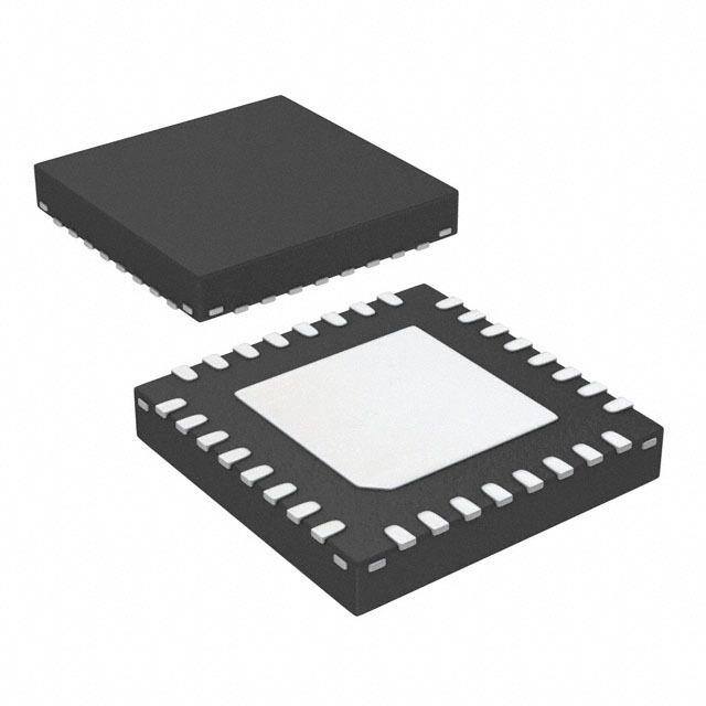
| 供应商器件封装 | 32-QFN(5x5) |
| 其它名称 | 1127-1193-1 |
| 功能 | 相移 |
| 包装 | 剪切带 (CT) |
| 封装/外壳 | 32-VFQFN 裸露焊盘 |
| 标准包装 | 1 |
| 辅助属性 | - |
| 频率 | 1GHz ~ 2GHz |
Datasheet
PDF Datasheet 数据手册内容提取
HMC934LP5E v01.1211 400° ANALOG PHASE SHIFTER 1 - 2 GHz Typical Applications Features the hMC934LP5e is ideal for: Octave Bandwidth: 1 to 2 Ghz t •EW Receivers 400° Phase shift M •Military Radar Low insertion Loss: 3.5 dB s E •Test Equipment Low Phase error: +3.5 / -2 deg - L •Satellite Communications single Positive Voltage Control a 32 Lead 5 x 5 mm QfN Package: 25 mm² t •Beam Forming Modules T i G Functional Diagram General Description i D the hMC934LEP5e is an analog Phase shifter which - is controlled via an analog control voltage from 0 to s +13V. the hMC934LP5e provides a continuously r variable phase shift of 0 to 400 degrees from 1 to 2 L e Ghz, with extremely consistent low insertion loss t versus phase shift and frequency. the high accuracy f hMC934LP5e is monotonic with respect to control i O h voltage and features a typical low phase error of s +3.5 / -2 degrees. the hMC934LP5e is housed in an e rohs compliant 5 x 5 mm QfN leadless package. s S a h P B Electrical Specifications, T = +25 °C, 50 Ohm System O A Parameter Min. typ. Max. Units frequency range 1 2 Ghz Phase shift range 400 deg insertion Loss 3.5 dB return Loss (input and output) 15 dB Control Voltage range 0 13 V Control Current range ±1 ma input iP3 30 dBm input Power @ -5° shift in insertion Phase (Vctl = 0V) 9 dBm input Power @ -5° shift in insertion Phase (Vctl = 0.5V) 13 dBm input Power @ -2° shift in insertion Phase (Vctl = 13V) 16 dBm Phase Voltage sensitivity 32 deg/V Phase error (peak) [1] +9 / -5 deg Phase error (average) [1] +3.5 / -2 deg Modulation Bandwidth 6 Mhz insertion Phase temperature sensitivity 0.16 deg/°C [1] Up to a phase shift of 360 degrees. For price, delivery and to place orders: Hittite Microwave Corporation, 2 Elizabeth Drive, Chelmsford, MA 01824 1 Phone: 978-250-3343 Fax: 978-250-3373 Order On-line at www.hittite.com Application Support: Phone: 978-250-3343 or apps@hittite.com
HMC934LP5E v01.1211 400° ANALOG PHASE SHIFTER 1 - 2 GHz Insertion Loss vs. Frequency Insertion Loss vs. Vctl , F = 1.5 GHz 0 -2 t -1 M -2 B) -3 -3 E s INSERTION LOSS (d-1------0987654 0036V.VV5V NSERTION LOSS (dB)--54 T++- 428055CCC GitaL - -11 91V3V I Di E -12 -6 0.5 0.75 1 1.25 1.5 1.75 2 2.25 2.5 0 1 2 3 4 5 6 7 8 9 10 11 12 13 FREQUENCY (GHz) Vctl (Vdc) - s Phase Shift vs. Frequency r L Phase Shift vs. Vctl @ Vctl = 6V (Relative to Vctl = 0V) e t 495 350 f ASE SHIFT (degrees) 223344271605505050 S O HASE SHIFT (degrees)233333901234000000 ++- 428055CCC se shi H P a ALIZED P 11389500 11 .G5 HGzHz MALIZED 222678000 Ph RM 45 B 2 GHz OR250 O N N 0 240 0 1 2 3 4 5 6 7 8 9 10 11 12 13 0.5 0.75 1 1.25 1.5 1.75 2 2.25 2.5 Vctl (Vdc) FREQUENCY (GHz) Phase Shift vs. FrOequency Phase Error vs. (Relative to Vctl = 0V) Vctl = 0 to 13V Frequency, Fmean = 1.5 GHz [1] 540 10 es)495 13V e gr450 E SHIFT (de334160505 R (degrees) 05 S270 O A R D PH128205 E ER -5 02.V5V LIZE135 HAS 46VV MA 90 P-10 89V.5V OR 45 Average N 1V 0 -15 0.5 0.75 1 1.25 1.5 1.75 2 2.25 2.5 1 1.1 1.2 1.3 1.4 1.5 1.6 1.7 1.8 1.9 2 FREQUENCY (GHz) FREQUENCY (GHz) [1] 0 to 9.5V provides 0 - 360 degrees phase shift range For price, delivery and to place orders: Hittite Microwave Corporation, 2 Elizabeth Drive, Chelmsford, MA 01824 Phone: 978-250-3343 Fax: 978-250-3373 Order On-line at www.hittite.com 2 Application Support: Phone: 978-250-3343 or apps@hittite.com
HMC934LP5E v01.1211 400° ANALOG PHASE SHIFTER 1 - 2 GHz Second Harmonic vs. Vctl, F = 1.5 GHz Third Harmonic vs. Vctl, F = 1.5 GHz t 80 80 M 70 - 10 dBm 70 0 dBm L - s ONIC (dBc)456000 + 10 dBm ONIC (dBc)456000 E a M M R R t HA30 HA30 T Gi 2ND 20 3RD 20 Pin: -10 dBm Pin: 0 dBm i 10 10 Pin: +10 dBm D E 0 0 0 1 2 3 4 5 6 7 8 9 10 11 12 13 0 1 2 3 4 5 6 7 8 9 10 11 12 13 - Vctl (Vdc) Vctl (Vdc) s r L e Input IP3 vs. Vctl, F = 1.5 GHz Insertion Loss vs. Pin @ 1 GHz t f 35 -2 i O h -3 s 30 B) d S ( -4 e m) S Phas INPUT IP3 (dB2205 - + 1010 0d dBdBBmmBm S INSERTION LO ---765 0061V.V35VV 15 -8 0 1 2 3 4 5 6 7 8 9 10 11 12 13 -4 -2 0 2 4 6 8 10 12 14 16 18 20 Vctl (Vdc) INPUT POWER (dBm) O Insertion Loss vs. Pin @ 1.5 GHz Insertion Loss vs. Pin @ 2 GHz -2 -2 -3 -3 B) B) d d S ( -4 S ( -4 S S O O L L N -5 N -5 O O TI TI INSER -6 006V.V5V INSER -6 006V.V5V -7 13V -7 13V -8 -8 -4 -2 0 2 4 6 8 10 12 14 16 18 20 -4 -2 0 2 4 6 8 10 12 14 16 18 20 INPUT POWER (dBm) INPUT POWER (dBm) For price, delivery and to place orders: Hittite Microwave Corporation, 2 Elizabeth Drive, Chelmsford, MA 01824 3 Phone: 978-250-3343 Fax: 978-250-3373 Order On-line at www.hittite.com Application Support: Phone: 978-250-3343 or apps@hittite.com
HMC934LP5E v01.1211 400° ANALOG PHASE SHIFTER 1 - 2 GHz Phase Shift vs. Pin @ 1 GHz Phase Shift vs. Pin @ 1.5 GHz 1 1 t s) s) ee 0 ee 0 M gr gr T (de -1 T (de -1 E s HIF -2 HIF -2 - SE S -3 SE S -3 L A A H -4 H -4 a D P -5 0V D P -5 T0V t ALIZE -6 061.V35VV ALIZE -6 061.V35VV Gi M M R -7 R -7 i O O D N N E -8 -8 -4 -2 0 2 4 6 8 10 12 14 16 -4 -2 0 2 4 6 8 10 12 14 16 - INPUT POWER (dBm) INPUT POWER (dBm) s Input Return Loss vs. r L Phase Shift vs. Pin @ 2 GHz Frequency, Vctl = 0 to +13V e t 1 0 f grees) -01 O hi e FT (d --32 dB)-10 s SHI -4 SS ( e SE -5 LO-20 s A -6 S N ALIZED PH ---987 00V.5V RETUR-30 0136VVVV Pha M-10 6V 9V R 13V B 13V O-11 N-12 -40 -4 -2 0 2 4 6 8 10 12 14 16 0.5 0.75 1 1.25 1.5 1.75 2 2.25 2.5 INPUT POWER (dBm) FREQUENCY (GHz) O Output Return Loss vs. Absolute Maximum Ratings Frequency, Vctl = 0 to +13V frequency Control Voltage (Vctl) -0.5 to +15V 0 rf input Power 27 dBm storage temperature -65 to +150 °C -10 B) esD sensitivity (hBM) Class 1B d S ( S O L-20 Reliability Information N R U RET-30 013VVV J1u Mnciltliioonn theomurp eMrtattufre to Maintain 150 °C 6V 9V Nominal Junction temperature 13V 87 °C (t = 85 °C and Pin = 10 dBm) -40 0.5 0.75 1 1.25 1.5 1.75 2 2.25 2.5 thermal resistance 45 °C/W FREQUENCY (GHz) (Junction to Ground Paddle) Operating temperature -40 to +85 °C eLeCtrOstatiC seNsitiVe DeViCe OBserVe haNDLiNG PreCaUtiONs For price, delivery and to place orders: Hittite Microwave Corporation, 2 Elizabeth Drive, Chelmsford, MA 01824 Phone: 978-250-3343 Fax: 978-250-3373 Order On-line at www.hittite.com 4 Application Support: Phone: 978-250-3343 or apps@hittite.com
HMC934LP5E v01.1211 400° ANALOG PHASE SHIFTER 1 - 2 GHz Outline Drawing t M s E - L a t T i G i D E - s r L e t f i O NOtes: h 1. LeaDfraMe MateriaL: COPPer aLLOY s 2. DiMeNsiONs are iN iNChes [MiLLiMeters]. 3. DiMeNsiON DOes NOt iNCLUDe MOLDfLash Of 0.15 mm Per siDe. e 4. DiMeNsiON DOes NOt iNCLUDe MOLDfLash Of 0.25 mm Per siDe. s S 5. aLL GrOUND LeaDs MUst Be sOLDereD tO PCB rf GrOUND. a 6. CLassifieD as MOistUre seNsitiVitY LeVeL (MsL) 1. h Package Information P Part Number PaBckage Body Material Lead finish MsL rating Package Marking [1] h934 hMC934LP5e rohs-Compliant Low stress injection Molded Plastic 100% Matte sn MsL1 [2] XXXX [1] 4-Digit lot number XXXX [2] Max peak reflow tempeOrature of 260 °C Pin Descriptions Pin Number function Description interface schematic 1 - 5, 8 - 13, No connection required. these pins may be connected to rf/DC N/C 15 - 17, 20 - 32 ground without affecting performance. Ground: Backside of package has exposed metal ground paddle 7, 18 GND that must be connected to ground thru a short path. Vias under the device are required. 6 rfiN this pin is aC coupled and matched to 50 Ohms. 19 rfOUt this pin is aC coupled and matched to 50 Ohms. Phase shift control pin. application of a voltage between 0 and 14 Vctl 13 volts causes the transmission phase to change. the DC equivalent circuit is a series connected diode and resistor. For price, delivery and to place orders: Hittite Microwave Corporation, 2 Elizabeth Drive, Chelmsford, MA 01824 5 Phone: 978-250-3343 Fax: 978-250-3373 Order On-line at www.hittite.com Application Support: Phone: 978-250-3343 or apps@hittite.com
HMC934LP5E v01.1211 400° ANALOG PHASE SHIFTER 1 - 2 GHz Evaluation PCB t M E s - L a T t i G i D E - s r L e t f O i h s e s S a h P B O List of Materials for Evaluation PCB 131046 [1] the circuit board used in the application should item Description use rf circuit design techniques. signal lines J1, J2 Connector, sMa, Jack should have 50 Ohm impedance while the package J3 Connector, sMa, Jack ground leads and exposed paddle should be con- U1 hMC934LP5e analog Phase shifter nected directly to the ground plane similar to that C1, C2 Capacitor, 100 pf, 0402 Pkg. shown. a sufficient number of via holes should be PCB 127338, evaluation PCB used to connect the top and bottom ground planes. [1] reference this number when ordering complete evaluation PCB the evaluation board should be mounted to an [2] Circuit Board Material: rogers 4350 or arlon 25 fr appropriate heat sink. the evaluation circuit board shown is available from hittite upon request. For price, delivery and to place orders: Hittite Microwave Corporation, 2 Elizabeth Drive, Chelmsford, MA 01824 Phone: 978-250-3343 Fax: 978-250-3373 Order On-line at www.hittite.com 6 Application Support: Phone: 978-250-3343 or apps@hittite.com