
 Datasheet下载
- 型号: ISL8206MIRZ
- 制造商: Intersil
- 库位|库存: xxxx|xxxx
- 要求:
| 数量阶梯 | 香港交货 | 国内含税 |
| +xxxx | $xxxx | ¥xxxx |
查看当月历史价格
查看今年历史价格
ISL8206MIRZ产品简介:
ICGOO电子元器件商城为您提供ISL8206MIRZ由Intersil设计生产,在icgoo商城现货销售,并且可以通过原厂、代理商等渠道进行代购。 ISL8206MIRZ价格参考。IntersilISL8206MIRZ封装/规格:直流转换器, 非隔离 PoL 模块 DC/DC 转换器 1 输出 0.6 ~ 6 V 6A 1V - 20V 输入。您可以下载ISL8206MIRZ参考资料、Datasheet数据手册功能说明书,资料中有ISL8206MIRZ 详细功能的应用电路图电压和使用方法及教程。
| 参数 | 数值 |
| 产品目录 | |
| 描述 | IC BUCK SYNC ADJ 6A 15QFN非隔离式DC/DC转换器 STAND ALONE 6A DC/DC STEPDWNPWRSUPPYMOD15 |
| 产品分类 | DC DC ConvertersDC/DC转换器 |
| 品牌 | Intersil |
| 产品手册 | |
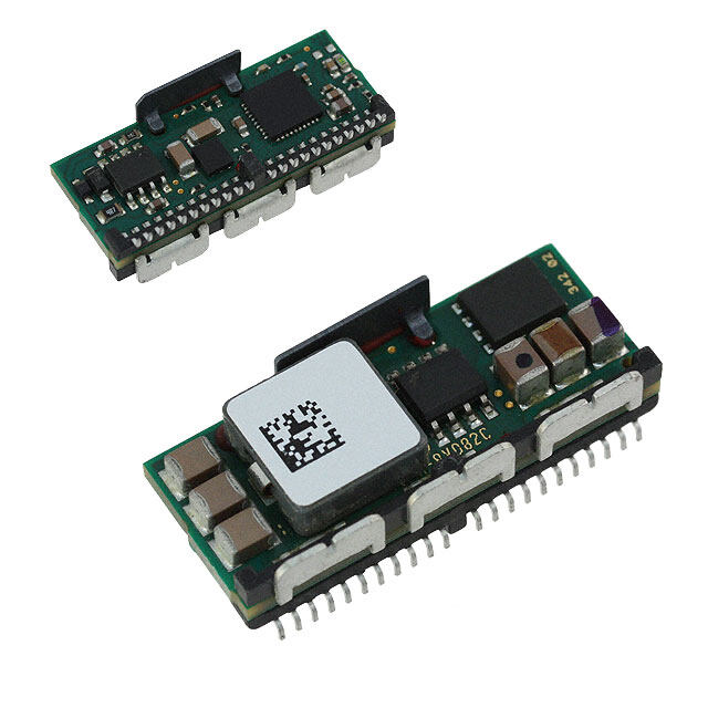
| 产品图片 |
|
| rohs | 否无铅 / 符合限制有害物质指令(RoHS)规范要求 |
| 产品系列 | 非隔离式DC/DC转换器,Intersil ISL8206MIRZ- |
| 数据手册 | |
| 产品型号 | ISL8206MIRZ |
| 产品培训模块 | http://www.digikey.cn/PTM/IndividualPTM.page?site=cn&lang=zhs&ptm=25593 |
| 产品目录页面 | |
| 产品种类 | 非隔离式DC/DC转换器 |
| 功率(W)-制造系列 | 36W |
| 功率(W)-最大值 | 36W |
| 包装 | 托盘 |
| 商标 | Intersil |
| 大小/尺寸 | 0.59" 长 x 0.59" 宽 x 0.14" 高(15.0mm x 15.0mm x 3.5mm) |
| 安装类型 | 表面贴装 |
| 安装风格 | SMD/SMT |
| 封装 | Tray |
| 封装/外壳 | 15-BQFN |
| 工作温度 | -40°C ~ 85°C |
| 工厂包装数量 | 96 |
| 效率 | 95% |
| 标准包装 | 96 |
| 特性 | - |
| 特色产品 | http://www.digikey.com/cn/zh/ph/Intersil/ISL8206M.html |
| 电压-输入(最大值) | 20V |
| 电压-输入(最小值) | 1V |
| 电压-输出1 | 0.6 ~ 6 V |
| 电压-输出2 | - |
| 电压-输出3 | - |
| 电压-隔离 | - |
| 电流-输出(最大值) | 6A |
| 类型 | 非隔离 PoL 模块 |
| 系列 | ISL8206M |
| 输入电压范围 | 1 V to 20 V |
| 输出数 | 1 |
| 输出电压—通道1 | 0.6 V to 6 V |
| 输出电流—通道1 | 6 A |
| 输出端数量 | 1 |


- 商务部:美国ITC正式对集成电路等产品启动337调查
- 曝三星4nm工艺存在良率问题 高通将骁龙8 Gen1或转产台积电
- 太阳诱电将投资9.5亿元在常州建新厂生产MLCC 预计2023年完工
- 英特尔发布欧洲新工厂建设计划 深化IDM 2.0 战略
- 台积电先进制程称霸业界 有大客户加持明年业绩稳了
- 达到5530亿美元!SIA预计今年全球半导体销售额将创下新高
- 英特尔拟将自动驾驶子公司Mobileye上市 估值或超500亿美元
- 三星加码芯片和SET,合并消费电子和移动部门,撤换高东真等 CEO
- 三星电子宣布重大人事变动 还合并消费电子和移动部门
- 海关总署:前11个月进口集成电路产品价值2.52万亿元 增长14.8%


PDF Datasheet 数据手册内容提取
DATASHEET ISL8204M, ISL8206M FN6999 Complete High Efficiency DC/DC Power Module Rev 4.00 October 28, 2014 The ISL8204M, ISL8206M is a family of pin-compatible power Features modules to the ISL8201M. These are simple and easy to use, high power DC/DC modules and are ideal for a wide variety of • Complete switch mode power supply in one package applications. The ISL820xM family of high current DC/DC - ISL8204M - 4A with, 6.6A Peak step-down modules virtually eliminate design and - ISL8206M - 6A with, 8.8A Peak manufacturing risks while dramatically improving time to • Single resistor sets V +0.6V up to +6V at ±1% market. OUT • Up to 95% efficiency The simplicity is in the family's "Off The Shelf" unassisted implementation. All you need is the ISL820xM for the current • Overcurrent protection requirement of your design, bulk input and output capacitors • Internal soft-start with pre-bias output start-up and one resistor, to program the output voltage, and you have • Wide input voltage range from 1VDC to 20VDC a complete high current power design ready for your market. • Fast transient response This family of buck converters is packaged in a thermally enhanced compact (15mmx15mm) overmolded QFN Package Applications that operates without a heatsink, even at full load over temperature. The package supports simple, reliable, • Servers automated assembly using standard surface mount • Telecom and datacom applications equipment while making it easy to probe to all pins. The lack • Industrial equipment of a required heat dissipation layer, provides easy access to all pins and the limited number of the external components • Point of load regulation reduce the PCB to a component layer and a simple ground • General purpose step-down DC/DC layer. Related Literature Additionally, each IC in the family is footprint compatible, making it easy to change your design to meet different power •AN1386 “ISL8201M, ISL8204M, ISL8206M EVAL1Z needs without changing your layout. One simple layout fits all. Evaluation Board User’s Guide” • iSim model - (See respective device information page at www.intersil.com) PVCC CPVCC 7 (1V tVoIN 2 0V) VIN PVCC10µF VOUT (0.6VV tOoU T6 . 0V) NT (A) 56 3.3V 220µF 330µF RE 4 1.5V R U 0.6V ISL8204M/6M C 3 D Power Module FB OA 2 L X RFB MA 1 (Sets V ) OUT 0 PGND 60 70 80 90 100 110 AMBIENT TEMPERATURE (°C) FIGURE 1. TYPICAL SCHEMATIC FIGURE 2. DERATING CURVE (ISL8206M 5V ) IN TABLE 1. R VALUES FOR TYPICAL OUTPUT VOLTAGES FB V 0.6V 1.05V 1.2V 1.5V 1.8V 2.5V 3.3V 5V OUT R Open 13k 9.76k 6.49k 4.87k 3.09k 2.16k 1.33k FB FN6999 Rev 4.00 Page 1 of 19 October 28, 2014
ISL8204M, ISL8206M Simplified Block Diagram PVCC VIN SAMPLE POR PGND HAONLDD SOFTA-NSDTART LDO - INHIBIT DRIVER + 21.5µA VOUT ISET 0.6V + GATE FB - +- PWM COLNOTGRICOL PVCC 0.4V + DIS - DRIVER COMP/EN OSCILLATOR RSET-IN PGND PWM Controller RFB-TI ISET PHASE FIGURE 3. INTERNAL BLOCK DIAGRAM Ordering Information PART NUMBER PART TEMP. PACKAGE PKG. (Notes1, 2, 3) MARKING RANGE (°C) (RoHS Compliant) DWG.# ISL8204MIRZ ISL8204M -40 to +85 15 Ld QFN L15.15x15 ISL8206MIRZ ISL8206M -40 to +85 15 Ld QFN L15.15x15 ISL8204MEVAL1Z Evaluation Board ISL8206MEVAL1Z Evaluation Board NOTES: 1. Add “-T*” suffix for tape and reel. Please refer to TB347 for details on reel specifications. 2. These Intersil plastic packaged products are RoHS compliant by EU exemption 7C-I and employ special Pb-free material sets, molding compounds/die attach materials, and 100% matte tin plate plus anneal (e3) termination finish which is compatible with both SnPb and Pb-free soldering operations. Intersil RoHS compliant products are MSL classified at Pb-free peak reflow temperatures that meet or exceed the Pb-free requirements of IPC/JEDEC J STD-020. 3. For Moisture Sensitivity Level (MSL), please see device information page for ISL8204M, ISL8206M. For more information on MSL please see techbrief TB363. Summary of Features RATED CURRENT R LS FET r MAX V ISET DS(ON) OUT PART NUMBER (A) (k) (m) (V) ISL8206M 6 4.12 15 6 ISL8204M 4 2.87 15 6 FN6999 Rev 4.00 Page 2 of 19 October 28, 2014
ISL8204M, ISL8206M Pin Configuration ISL8204M, ISL8206M (15 LD QFN) TOP AND 3D VIEW C D D D VIN NC ISET NC PVC PGN PGN PGN 9 8 7 6 5 4 3 2 1 PGND 15NC PD1 14FB 13COMP/EN PHASE10 PD2 PD4 12VOUT PD3 11 PGND Pin Descriptions PIN SYMBOL DESCRIPTION 1, 2, 3, 4 PGND Power ground pin for signal, input, and output return path. PGND needs to connect to one (or more) ground plane(s) immediately, which is recommended to minimize the effect of switching noise, copper losses, and maximize heat dissipation. Range: 0V. 5 PVCC This pin provides the bias supply for ISL8204M, ISL8206M, as well as the low-side MOSFET’s gate and high-side MOSFET’s gate. If PVCC rises above 6.5V, an internal 5V regulator will supply to the internal logics bias (but high-side and low-side MOSFET gate will still be sourced by PVCC). Connect a well decoupled +5V or +12V supply to this pin. Connect 1µF ceramic capacitor to ground plane directly. Range: 4.5V to 14.4V. 6, 8, 15 NC No internal connection. The ISET pin is the input for the overcurrent protection (OCP) setting, which compares the r of the low-side DS(ON) MOSFET to set the overcurrent threshold. The ISL8204M, ISL8206M has an initial protect overcurrent limit. It has an 7 ISET integrated internal 4.12k2.87k resistor (R ) between the ISET and PGND pins, which can prevent significant SET-IN overcurrent impact to the module. One can also connect an additional resistor R between the ISET pin and the SET-EX PGND pin in order to reduce the current limit point by paralleling. Range: 0 to PVCC. 9 VIN Power input pin. Apply input voltage between the VIN pin and PGND pin. It is recommended to place an input decoupling (PD1) capacitor directly between the VIN pin and the PGND pin. The input capacitor should be placed as closely as possible to the module. Range: 1V to 20V. 10 PHASE The PHASE pin is the switching node between the high and low-side MOSFET. It also returns the current path for the (PD2) high-side MOSFET driver and detects the low-side MOSFET drain voltage for the overcurrent limits point. Range: 0V to 30V. 11 PGND Power ground pin for signal, input, and output return path. PGND needs to connect to one (or more) ground plane(s) (PD3) immediately, which is recommended to minimize the effect of switching noise, copper losses, and maximize heat dissipation. Range: 0V. 12 VOUT Power output pin. Apply output load between this pin and the PGND pin. It is recommended to place a high frequency (PD4) output decoupling capacitor directly between the VOUT pin and the PGND pin. The output capacitor should be placed as closely as possible to the module. Range: 0.6V to 6V. FN6999 Rev 4.00 Page 3 of 19 October 28, 2014
ISL8204M, ISL8206M Pin Descriptions (Continued) PIN SYMBOL DESCRIPTION 13 COMP/EN This is the multiplexed pin of the ISL8204M, ISL8206M. During soft-start and normal converter operation, this pin represents the output of the error amplifier. Use COMP/EN in combination with the FB pin to compensate for the voltage control feedback loop of the converter. Pulling COMP/EN low (V = 0.4V nominal) will disable (shutdown) the controller, ENDIS which causes the oscillator to stop, and the high-side gate and low-side gate of the MOSFETs outputs to be held low. The external pull-down device will initially need to overcome a maximum of 5mA of COMP/EN output current. However, once the controller is disabled, the COMP/EN output will also be disabled, thus only a 20µA current source will continue to draw current. Range: 0V to 5V. 14 FB The FB pin is the output voltage adjustment of the ISL8204M, ISL8206M. It will regulate to 0.6V at the FB pin with respect to the PGND pin. The ISL8204M, ISL8206M has an integrated voltage dividing resistor. This is a precision 9.76kΩ resistor (RFB-TI) between the VOUT and FB pins. Different output voltages can be programmed with additional resistors between FB to PGND. Range: 0.6V. FN6999 Rev 4.00 Page 4 of 19 October 28, 2014
ISL8204M, ISL8206M Absolute Maximum Ratings Thermal Information COMP/EN to PGND. . . . . . . . . . . . . . . . . . . . . . . . . . . . . . . . PGND - 0.3V to +6V Thermal Resistance (Typical) JA (°C/W) JC (°C/W) ISET to PGND . . . . . . . . . . . . . . . . . . . . . . . . . . . . . PGND - 0.3V to PVCC + 0.3V 15 Ld QFN (Notes5, 6) . . . . . . . . . . . . . . . . 13.0 2.0 PVCC to PGND . . . . . . . . . . . . . . . . . . . . . . . . . . . . . . . . . . PGND - 0.3V to +15V Pb-Free Reflow Profile . . . . . . . . . . . . . . . . . . . . . . . . . . . . . . . . . . see TB493 P to P (Note4). . . . . . . . . . . . . . . . . . . . . . . . . . . . . . . . -1.2V ~ +30V HASE GND V to P (Note4). . . . . . . . . . . . . . . . . . . . . . . . . . . . . . . . . . -1.2V ~ +30V IN HASE Junction Temperature, T . . . . . . . . . . . . . . . . . . . . . . . . . . . . . . . . . . +125°C J Recommended Operating Ratings Storage Temperature Range, T . . . . . . . . . . . . . . . . . . -55°C to +125°C STG ESD Rating Input Supply Voltage (V ) . . . . . . . . . . . . . . . . . . . . . . . . . . . . . +1V to +20V IN Human Body Model (Tested per JESD22-A114E). . . . . . . . . . . . . . . . 2kV Output Voltage (V ). . . . . . . . . . . . . . . . . . . . . . . . . . . . . . . . . +0.6V to +6V OUT Machine Model (Tested per JESD22-A115-A). . . . . . . . . . . . . . . . . 100V P VCC Charge Device Model (Tested per JESD22-C101C). . . . . . . . . . . . . . . 1kV Fixed Supply Voltage . . . . . . . . . . . . . . . . . . . . . . . . . . . . . . . +5V or +12V Latch Up (Tested per JESD-78B; Class 2, Level A) . . . . . . . . . . . . . . 100mA Wide Range Supply . . . . . . . . . . . . . . . . . . . . . . . . . . . . . +6.5V to +14.4V Ambient Temperature Range (T ) . . . . . . . . . . . . . . . . . . . -40°C to +85°C A CAUTION: Do not operate at or near the maximum ratings listed for extended periods of time. Exposure to such conditions may adversely impact product reliability and result in failures not covered by warranty. NOTES: 4. V (Drain to Source) specification for internal high-side and low-side MOSFET. DS 5. is measured in free air with the component mounted on a high effective thermal conductivity test board (i.e. 4-layer type without thermal vias JA – see tech brief TB379) per JEDEC standards except that the top and bottom layers assume solid planes. 6. For , the “case temp” location is the center of the exposed metal pad on the package underside. JC Electrical Specifications T = +25°C. V = 12V, V = 1.5V. C = 220µFx1, 10µF/Ceramicx2, C =47µFx8/Ceramic. Boldface limits A IN OUT IN OUT apply over the operating temperature range, -40°C to +85°C. MIN MAX PARAMETER SYMBOL CONDITIONS (Note8) TYP (Note8) UNITS INPUT CHARACTERISTICS Input Supply Bias Current I I = 0A, V = 1.5V, V = 12V, P = 12V - 13 - mA Q(VIN) OUT OUT IN VCC Input In-rush Current I I = 0A, V = 1.5V, V = 12V, P = 12V - 140 - mA inRush OUT OUT IN VCC Input Supply Current I I = 6A, V = 1.5V, V = 12V, P = 12V - 0.86 - A S(VIN) OUT OUT IN VCC I = 4A, V = 1.5V, V = 12V, P = 12V - 0.56 - A OUT OUT IN VCC OUTPUT CHARACTERISTICS Output Continuous Current Range I V = 12V, V = 1.5V 0 - OUT(DC) IN OUT ISL8206M 6 A ISL8204M 0 - 4 A Line Regulation Accuracy V /V V = 1.5V, I = 0A, V = 3.3V to 20V, - 0.1 - % OUT IN OUT OUT IN P = 5V VCC Load Regulation Accuracy V /I I = 0A to 6A/4A, V = 1.5V, V =12V, - 0.5 - % OUT OUT OUT OUT IN P = 12V VCC Peak-to-Peak Output Ripple Voltage V ISL8206M - 8 - mV OUT I = 6A V = 1.5V, V = 12V, OUT OUT IN P = 12V VCC ISL8204M - 7 - mV I = 4A V = 1.5V, V = 12V, OUT OUT IN P = 12V VCC DYNAMIC CHARACTERISTICS Voltage Change For Positive Load Step V I = 0A to 4A. Current slew rate=2.5A/µs, - 30 - mV OUT-DP OUT V = 12V, V = 1.5V, P =12V IN OUT VCC Voltage Change For Negative Load Step V I = 0A to 4A. Current slew rate=2.5A/µs, - 27 - mV OUT-DN OUT V = 12V, V = 1.5V, P =12V IN OUT VCC FN6999 Rev 4.00 Page 5 of 19 October 28, 2014
ISL8204M, ISL8206M Electrical Specifications T = +25°C. V = 12V, V = 1.5V. C = 220µFx1, 10µF/Ceramicx2, C =47µFx8/Ceramic. Boldface limits A IN OUT IN OUT apply over the operating temperature range, -40°C to +85°C. (Continued) MIN MAX PARAMETER SYMBOL CONDITIONS (Note8) TYP (Note8) UNITS Voltage Change For Positive Load Step V I = 0A to 6A. Current slew rate=2.5A/µs, - 43 - mV OUT-DP OUT V = 12V, V = 1.5V, P =12V IN OUT VCC Voltage Change For Negative Load Step V I = 0A to 6A. Current slew rate=2.5A/µs, - 40 - mV OUT-DN OUT V = 12V, V = 1.5V, P =12V IN OUT VCC CONTROLLER PVCC Supply Current Shutdown I P = 12V; Disabled (Note7) 4 5.2 7 mA PVCC_S VCC Supply Voltage P Fixed 5V supply (Note7) 4.5 5.0 5.5 V VCC Wide range supply (Note7) 6.5 12.0 14.4 V P Operating Current I I = 6A, V = 1.5V, V =12V VCC PVCC OUT OUT IN 5V supply - 14 - mA 12V supply - 25 - mA I = 4A, V = 1.5V, V =12V OUT OUT IN 5V supply - 14 - mA 12V supply - 25 - mA Rising P Threshold V (Note7) 3.9 4.1 4.3 V VCC PORR P Power-On-Reset Threshold Hysteresis V (Note7) 0.30 0.35 0.40 V VCC PORH Oscillator Frequency F (Note7) 510 600 660 kHz OSC Internal Resistor Between V and FB Pins R (Note7) 9.66 9.76 9.86 k OUT FB-TI Disabled Threshold Voltage (COMP/EN) V (Note7) 0.375 0.4 0.425 V ENDIS Reference Voltage V (Note7) - 0.6 - V REF Reference Voltage Tolerance 0°C to +70°C (Note7) -1.0 - +1.0 % -40°C to +85°C (Note7) -1.5 - +1.5 % FAULT PROTECTION Internal Resistor Between I and P Pins R ISL8206M - 4.12 - k SET GND SET-IN ISL8204M - 2.87 - k I Current Source I (Note7) 18.0 21.5 23.5 µA SET SET NOTES: 7. Parameters are 100% tested for internal IC/component prior to module assembly. 8. Parameters with MIN and/or MAX limits are 100% tested at +25°C, unless otherwise specified. Temperature limits established by characterization and are not production tested. FN6999 Rev 4.00 Page 6 of 19 October 28, 2014
ISL8204M, ISL8206M C PVCC PVCC V OUT V IN 1.8V (+5V/+12V) 10A VIN VOUT ISL8204M, CIN (BULK) CIN (CER) ISL8206M COUT1 COUT2 220µF 10µF 22µF 330µF PHASE COMP/EN 25V 6.3V x2 x3 ISET FB PGND R FB 4.87k FIGURE 4. TEST CIRCUIT FOR ALL PERFORMANCE AND DERATING GRAPHS Typical Performance Characteristics Efficiency Performance T = +25°C, V = P (P = 5V for 18V ), C = 220µFx1, 10µF/Ceramic x 2, C = 330µF (ESR = 10m), A IN VCC VCC IN IN OUT 22µF/Ceramic x 3. Theefficiency equation is: Output Power POUT VOUTxIOUT Efficiency = ----------------------------------------- = ---------------- = -------------------------------------- Input Power P V xI IN IN IN 100 100 95 95 90 90 %) %) Y ( 85 Y ( 85 C C EN 80 3.3V EN 80 CI 2.5V CI FFI 75 1.5V FFI 75 E 70 E 70 3.3V 1.2V 2.5V 65 0.8V 65 5.0V 1.5V 1.2V 0.8V 60 60 0 1 2 3 4 5 6 0 1 2 3 4 5 6 LOAD CURRENT (A) LOAD CURRENT (A) FIGURE 5. EFFICIENCY vs LOAD CURRENT (5V ) FIGURE 6. EFFICIENCY vs LOAD CURRENT (12V ) IN IN 100 95 90 %) Y ( 85 C EN 80 CI FI 75 EF 70 5.0V 3.3V 2.5V 1.5V 1.2V 65 60 0 1 2 3 4 5 6 LOAD CURRENT (A) FIGURE 7. EFFICIENCY vs LOAD CURRENT (18V ) IN FN6999 Rev 4.00 Page 7 of 19 October 28, 2014
ISL8204M, ISL8206M Typical Performance Characteristics (Continued) Transient Response Performance T = +25°C, V = 12V, P = 12V, C =220µFx1, 10µF/Ceramic x 2, C =330µF A IN VCC IN OUT (ESR = 10mΩ), 22µF/Ceramic x 3 I = 0A to 5A, Current slew rate = 2.5A/µs OUT VOUT VOUT VIN = 12V VIN = 12V VOUT = 1.2V VOUT = 1.5V IOUT IOUT = 0A to 5A IOUT IOUT = 0A to 5A FIGURE 8. 1.2V TRANSIENT RESPONSE FIGURE 9. 1.5V TRANSIENT RESPONSE VOUT VOUT VIN = 12V VIN = 12V VOUT = 1.8V VOUT = 2.5V IOUT IOUT = 0A to 5A IOUT IOUT = 0A to 5A FIGURE 10. 1.8V TRANSIENT RESPONSE FIGURE 11. 2.5V TRANSIENT RESPONSE VOUT VIN = 12V VOUT = 3.3V IOUT IOUT = 0A to 5A FIGURE 12. 3.3V TRANSIENT RESPONSE FN6999 Rev 4.00 Page 8 of 19 October 28, 2014
ISL8204M, ISL8206M Typical Performance Characteristics (Continued) Output Ripple Performance T = +25°C, V = 1.5V, C = 220µFx1, 10µF/Ceramic x 2, C = 47µF/Ceramic x 8. A OUT IN OUT Oscilloscope BW = 20MHz VOUT 6A VOUT 6A VOUT 4A VOUT 4A VOUT 0A VOUT 0A FIGURE 13. OUTPUT VOLTAGE RIPPLE AT V = 5V FIGURE 14. OUTPUT VOLTAGE RIPPLE AT V = 12V IN IN Reference Circuitry For General 2. Separated Power Supply Applications Figure16 shows the ISL8204M, ISL8206M application schematic for wide input voltages from +1V to +20V. The 1. Single Power Supply PVCC supply can source +5V/+12V or +6.5V to 14.4V. Figure15 shows the ISL8204M, ISL8206M application (+5V/+12V) schematic for input voltage +5V or +12V. The PVCC pin can or PVCC connect to the input supply directly. (+6.5V to 14.4V) CPVCC CPVCC PVCC (+1V to +20V) COMP/EN VIN VIN PVCC ISL8204M, ISL8206M CIN FB PHASE (+5V/+12V) CISOLM8P20/E4NM, ISL8206VMIN CIN VIN ISET VOUT VOUT FB PHASE RFB RSET-EX PGND COUT VOUT ISET VOUT RFB RSET-EX PGND COUT FIGURE 16. WIDE INPUT VOLTAGE APPLICATION SCHEMATIC Applications Information FIGURE 15. TYPICAL APPLICATION SCHEMATIC The typical ISL8204M, ISL8206M application schematic for input voltage +5V or +12V is shown in Figure15. External component selection is primarily determined by the maximum load current and input/output voltage. Programming the Output Voltage The ISL8204M, ISL8206M has an internal 0.6V ±1.5% reference voltage. Programming the output voltage requires a dividing resistor (R ). The output voltage can be calculated as shown in FB Equation1: V = 0.61+9----.--7---6----k-- (EQ. 1) OUT R FB FN6999 Rev 4.00 Page 9 of 19 October 28, 2014
ISL8204M, ISL8206M Note: ISL8204M, ISL8206M has integrated 9.76k resistance into bias regulator can turn on cleanly. At the same time, the ISET pin the module (dividing resistor for top side). The resistance is initialized by disabling the low-side gate driver and drawing I SET corresponding to different output voltages is as shown in Table2: (nominal 21.5µA) through R . This sets up a voltage that will SETI represent the I trip point. At t , there is a variable time period SET 2 TABLE 2. RESISTANCE TO OUTPUT VOLTAGES for the OCP sample and hold operation (0.0ms to 3.4ms V 0.6V 0.8V 1.05V 1.2V nominal; the longer time occurs with the higher overcurrent OUT setting). The sample and hold operation uses a digital counter R open 28.7k 13k 9.76k FB and DAC to save the voltage, so the stored value does not degrade, as long as the P is above V (see “Overcurrent VOUT 1.5V 1.8V 2.5V 3.3V VCC PORR Protection (OCP)” on page12 for more details on the equations R 6.49k 4.87k 3.09k 2.16k FB and variables). Upon the completion of sample and hold at T , 3 the soft-start operation is initiated, and the output voltage ramps V 5V 6V OUT up between t and t . 4 5 R 1.33k 1.07k FB CCOOMMPP/E/NEN Initialization (POR and OCP Sampling) Figure17 shows a start-up waveform of ISL8204M, ISL8206M. Tt00 Tt11 The power-on-reset (POR) function continually monitors the bias voltage at the PVCC pin. Once the rising POR threshold has exceeded 4V (V nominal), the POR function initiates the IISSEETT PORR overcurrent protection (OCP) sample and hold operation (while COMP/EN is ~1V). When the sampling is complete, V begins the soft-start ramp. OUT VVOOUUT T PVCC FIGURE 18. I AND SOFT-START OPERATION SET VOUT ~4V START SWITCHING COMP/EN t1 t2 t3 t4 t5 COMP/EN FIGURE 17. POR AND SOFT-START OPERATION ISET If the COMP/EN pin is held low during power-up, the initialization VOUT will be delayed until the COMP/EN is released and its voltage rises above the V trip point. ENDIS 3.4ms 3.4ms Figures18 and 19 show a typical power-up sequence in more detail. The initialization starts at t , when either P rises above 0 VCC V , or the COMP/EN pin is released (after POR). The PORR FIGURE 19. ISET AND SOFT-START OPERATION COMP/EN will be pulled up by an internal 20µA current source, however, the timing will not begin until the COMP/EN exceeds the V trip point (at t ). The external capacitance of the Soft-Start and Pre-Biased Outputs ENDIS 1 disabling device, as well as the compensation capacitors, will The soft-start internally ramps the reference on the non-inverting determine how quickly the 20µA current source will charge the terminal of the error amp from 0V to 0.6V in a nominal 6.8ms. COMP/EN pin. With typical values, it should add a small delay The output voltage will follow the ramp from zero to its final value compared to the soft-start times. The COMP/EN will continue to in the same 6.8ms (the actual ramp seen on V will be less OUT ramp to ~1V. than the nominal time), due to some initialization timing From t1, there is a nominal 6.8ms delay, which allows the PVCC between t3 and t4. pin to exceed 6.5V (if rising up towards 12V), so that the internal FN6999 Rev 4.00 Page 10 of 19 October 28, 2014
ISL8204M, ISL8206M The ramp is created digitally, so there will be 64 small discrete steps. There is no simple way to change this ramp rate externally. After an initialization period (t to t ), the error amplifier (COMP/EN 3 4 pin) is enabled and begins to regulate the converter's output voltage during soft-start. The oscillator's triangular waveform is compared to the ramping error amplifier voltage. This generates PHASE pulses of VOUT increasing width that charge the output capacitors. When the internally generated soft-start voltage exceeds the reference voltage (0.6V), the soft-start is complete and the output should be in regulation at the expected voltage. This method provides a rapid and controlled output voltage rise; there is no large in-rush current charging the output capacitors. The entire start-up sequence from POR typically takes up to 17ms; up to 10.2ms for the delay and OCP sample and 6.8ms for the soft-start ramp. Figure20 shows the normal curve for start-up; initialization begins at t , and the output ramps between t and t . If the 0 1 2 output is pre-biased to a voltage less than the expected value (as shown Figure21), neither internal MOSFET will turn on until the soft-start ramp voltage exceeds the output; V starts OUT FIGURE 21. PRE-BIASED START-UP seamlessly ramping from there. VOUT VOUT T2 T0 T1 500mV/DIV FIGURE 20. NORMAL START-UP FIGURE 22. PRE-BIASED START-UP - OVERCHARGED If the output is pre-biased to a voltage above the expected value (as shown Figure22), neither MOSFET will turn on until the end of the soft-start, at which time it will pull the output voltage down to If VIN for the synchronous buck converter is from a different the final value. Any resistive load connected to the output will help supply that comes up after PVCC, the soft-start will go through its pull down the voltage (at the RC rate of the R of the load and the C cycle, but with no output voltage ramp. When VIN turns on, the of the output capacitance). output will follow the ramp of the VIN from zero up to the final expected voltage (at close to 100% duty cycle, with COMP/EN pin >4V). If V is too fast, there may be excessive in-rush current IN charging the output capacitors (only the beginning of the ramp, from zero to V matters here). If this is not acceptable, then OUT consider changing the sequencing of the power supplies, sharing the same supply, or adding sequencing logic to the COMP/EN pin to delay the soft-start until the V supply is ready (see “Input IN Voltage Considerations” on page13). If ISL8204M, ISL8206M is disabled after soft-start (by pulling COMP/EN pin low), and afterwards enabled (by releasing the COMP/EN pin), then the full initialization (including OCP sample) will take place. However, there is no new OCP sampling during FN6999 Rev 4.00 Page 11 of 19 October 28, 2014
ISL8204M, ISL8206M overcurrent retries. If the output is shorted to GND during Note: ISL8204M, ISL8206M has integrated 4.12k2.87k soft-start, the OCP will handle it, as described in the next section. resistance (R ). Therefore, the equivalent resistance of R SET-IN SET can be expressed in Equation3: Overcurrent Protection (OCP) R R SET-EX SET-IN R = ------------------------------------------------------- (EQ. 3) The overcurrent function protects the converter from a shorted SET R +R SET-EX SET-IN output by using the low-side MOSFET ON-resistance, r , to DS(ON) monitor the current. A resistor (R ) programs the overcurrent The scale factor of 2 doubles the trip point of the MOSFET voltage SET trip level. drop, compared to the setting on the RSET resistor. The OC trip point varies in a system mainly due to the MOSFET r DS(ON) This method enhances the converter's efficiency and reduces variations (i.e. over process, current and temperature). To avoid cost by eliminating a current sensing resistor. If overcurrent is overcurrent tripping in the normal operating load range, find the detected, the output immediately shuts off. It cycles the soft-start R resistor from Equation3, and use the following values: SET function in a hiccup mode (2dummy soft-start time-outs, then up to one real one) to provide fault protection. If the shorted 1. The maximum rDS(ON) at the highest junction temperature condition is not removed, this cycle will continue indefinitely. 2. The minimum I from the “Electrical Specifications” table SET on page3. Following POR (and 6.8ms delay), the ISL8204M, ISL8206M initiates the overcurrent protection sample and hold operation. 3. Determine IPEAK for: The low-side gate driver is disabled to allow an internal 21.5µA I L current source to develop a voltage across RSET. The ISL8204M, IPEAKIOUTMAX+------2------- (EQ. 4) ISL8206M samples this voltage (which is referenced to the PGND pin) at the ISET pin, and holds it in a counter and DAC where IL is the output inductor ripple current. In a high input combination. This sampled voltage is held internally as the voltage, high output voltage application, such as 20V input to 5V overcurrent set point, for as long as power is applied, or until a output, the inductor ripple becomes excessive due to the fix new sample is taken after coming out of a shutdown. internal inductor value. In such applications, the output current will be limited from the rating to approximately 70% of the module’s The actual monitoring of the low-side MOSFET ON-resistance rated current. starts 200ns (nominal) after the edge of the internal PWM logic signal (that creates the rising external low-side gate signal). This The relationships between the external RSET values and the is done to allow the gate transition noise and ringing on the typical output current IOUT(MAX) OCP levels for ISL8206M are as PHASE pin to settle out before monitoring. The monitoring ends follows: when the internal PWM edge (and thus low-side gate signal) goes TABLE 3. low. The OCP can be detected anywhere within the above window. OCP (A) at OCP (A) at R V = 12V, V = 12V SET IN IN If the converter is running at high duty cycles, around 75% for () PVCC = 5V PVCC = 12V 600kHz operation, then the low-side gate pulse width may not be OPEN 8.1 8.8 wide enough for the OCP to properly sample the r . For those DS(ON) 50k 7.5 8.1 cases, if the low-side gate signal is too narrow (or not there at all) for 3 consecutive pulses, then the third pulse will be stretched 20k 6.6 7.4 and/or inserted to the 425ns minimum width. This allows for 10k 5.5 6.4 OCP monitoring every third pulse under this condition. This can 5k 4.4 5.0 introduce a small pulse-width error on the output voltage, which will be corrected on the next pulse; and the output ripple voltage The range of allowable voltages detected (2 x I x R ) is 0mV to will have an unusual 3-clock pattern, which may look like jitter. SET SET 475mV. If the voltage drop across R is set too low, the following SET The overcurrent function will trip at a peak inductor current conditions may occur: (1)Continuous OCP tripping and retry and (IPEAK) determined by Equation2: (2) It may be overly sensitive to system noise and in-rush current 2I R spikes, so it should be avoided. The maximum usable setting is SET SET IPEAK = -----------r--------------------------------- (EQ. 2) around 0.2V across RSET (0.4V across the MOSFET); values above DSON this might disable the protection. Any voltage drop across R SET where: that is greater than 0.3V (0.6V MOSFET trip point) will disable the OCP. Note that conditions during power-up or during a retry may I is the internal I current source (21.5µA typical). SET SET look different than normal operation. During power-up in a 12V R is equivalent resistance between ISET and PGND pins. system, the ISL8204M, ISL8206M starts operation just above 4V; SET if the supply ramp is slow, the soft-start ramp might be over well r is typically 15m at (V = V = 10V, I =15A) and DS(ON) PVCC GS DS before 12V is reached. Therefore, with low-side gate drive voltages, 18m at (V = V = 4.5V, I =15A). PVCC GS DS the r of the MOSFET will be higher during power-up, DS(ON) effectively lowering the OCP trip. In addition, the ripple current will likely be different at a lower input voltage. Another factor is the digital nature of the soft-start ramp. On each discrete voltage step, there is in effect, a small load transient and a current spike to charge the output capacitors. The height of the current spike is not FN6999 Rev 4.00 Page 12 of 19 October 28, 2014
ISL8204M, ISL8206M controlled, however, it is affected by the step size of the output and typical power supply to ramp up past 6.5V before the soft-start the value of the output capacitors, as well as the internal error ramps begins. This prevents a disturbance on the output, due to amp compensation. Therefore, it is possible to trip the overcurrent the internal regulator turning on or off. If the transition is slow (not with in-rush current, in addition to the normal load and ripple a step change), the disturbance should be minimal. Thus, while the considerations. recommendation is to not have the output enabled during the transition through this region, it may be acceptable. The user Figure23 shows the output response during a retry of an output should monitor the output for their application to see if there is any shorted to PGND. At time t , the output has been turned off due to 0 problem. If P powers up first and V is not present by the time sensing an overcurrent condition. There are two internal soft-start VCC IN the initialization is done, then the soft-start will not be able to delay cycles (t and t ) to allow the MOSFETs to cool down in order 1 2 ramp the output, and the output will later follow part of the V to keep the average power dissipation in retry at an acceptable IN ramp when it is applied. If this is not desired, then change the level. At time t , the output starts a normal soft-start cycle, and the 2 sequencing of the supplies, or use the COMP/EN pin to disable output tries to ramp. If the short is still applied and the current V until both supplies are ready. reaches the I trip point any time during the soft-start ramp OUT SET period, the output will shut off and return to time t for another Figure24 shows a simple sequencer for this situation. If P 0 VCC delay cycle. The retry period is thus two dummy soft-start cycles powers up first, Q will be off, and R pulling to P will turn Q 1 3 VCC 2 plus one variable (which depends on how long it takes to trip the on, keeping the ISL8204M, ISL8206M in shutdown. When V IN sensor each time). Figure23 shows an example where the output turns on, the resistor divider R and R determine when Q turns 1 2 1 gets about half-way up before shutting down; therefore, the retry on, which will turn off Q and release the shutdown. If V powers 2 IN (or hiccup) time will be around 17ms. The minimum should be up first, Q will be on, turning Q off; so the ISL8204M, 1 2 nominally 13.6ms and the maximum 20.4ms. If the short ISL8206M will start up as soon as P comes up. The V trip VCC ENDIS condition is finally removed, the output should ramp up normally point is 0.4V nominal, so a wide variety of N-MOSFET or NPN BJT on the next t cycle. or even some logic IC's can be used as Q or Q . However, Q 2 1 2 2 must be low leakage when off (open-drain or open-collector) so as not to interfere with the COMP output. Q should also be 2 placed near the COMP/EN pin. VIN PVCC R3 T0 T1 T2 R1 TO COMP/EN ~6.8ms ~6.8ms R2 VOUT Q1 Q2 FIGURE 24. SEQUENCE CIRCUIT FIGURE 23. OVERCURRENT RETRY OPERATION The VIN range can be as low as ~1V (for VOUT as low as the 0.6V reference) and as high as 20V. There are some restrictions for Starting up into a shorted load looks the same as a retry into that running high V voltage. The maximum PHASE voltage is 30V. same shorted load. In both cases, OCP is always enabled during IN V + P + any ringing or other transients on the PHASE pin soft-start; once it trips, it will go into retry (hiccup) mode. The IN VCC must be less than 30V. If V is 20V, it is recommended to limit retry cycle will always have two dummy time-outs, plus whatever IN P to 5V. fraction of the real soft-start time passes before the detection VCC and shutoff. At that point, the logic immediately starts a new two Switching Frequency dummy cycle time-out. The switching frequency is a fixed 600kHz clock, which is Input Voltage Considerations determined by the internal oscillator. However, all of the other timing mentioned (POR delay, OCP sample, soft-start, etc.) is Figure16 shows a standard configuration where P is either 5V VCC independent of the clock frequency (unless otherwise noted). (±10%) or 12V (±20%). In each case, the gate drivers use the P voltage for low-side gate and high-side gate driver. In VCC Selection of the Input Capacitor addition, P is allowed to work anywhere from 6.5V up to the VCC 14.4V maximum. The P range between 5.5V and 6.5V is not The input filter capacitor should be based on how much ripple VCC allowed for long-term reliability reasons, but transitions through the supply can tolerate on the DC input line. The larger the it to voltages above 6.5V are acceptable. capacitor, the less ripple expected but consideration should be taken for the higher surge current during power-up. The There is an internal 5V regulator for bias, which turns on between ISL8204M, ISL8206M provides the soft-start function that 5.5V and 6.5V. Some of the delay after POR is there to allow a FN6999 Rev 4.00 Page 13 of 19 October 28, 2014
ISL8204M, ISL8206M controls and limits the current surge. The value of the input • The ground connection between pin 11 and pins 1 through 4 capacitor can be calculated by Equation5: should be a solid ground plane under the module. I t IN • Place a high frequency ceramic capacitor between (1) VIN and C = ------------------- (EQ. 5) IN V PGND (pin 11) and (2) PVCC and PGND (pins 1 through 4) as close to the module as possible to minimize high frequency Where: noise. CIN is the input capacitance (µF) • Use large copper areas for a power path (VIN, PGND, VOUT) to minimize conduction loss and thermal stress. Also, use I is the input current (A) IN multiple vias to connect the power planes in different layers. t is the turn on time of the high-side switch (µs) • Keep the trace connection to the feedback resistor short. V is the allowable peak-to-peak voltage (V) • Avoid routing any sensitive signal traces near the PHASE node. In addition to the bulk capacitance, some low Equivalent Series Inductance (ESL) ceramic capacitance is recommended to decouple between the drain terminal of the high-side MOSFET CPVCC PGND and the source terminal of the low-side MOSFET. This is used to reduce the voltage ringing created by the switching current across parasitic circuit elements. VIN Output Capacitors RFB The ISL8204M, ISL8206M is designed for low output voltage ripple. The output voltage ripple and transient requirements can VOUT be met with bulk output capacitors (C ) with low enough Equivalent Series Resistance (ESR). COUT can be a low ESR CIN OUT tantalum capacitor, a low ESR polymer capacitor or a ceramic COUT1 capacitor. The typical capacitance is 330µF and decoupled (DECOUPLE) ceramic output capacitors are used. The internally optimized loop compensation provides sufficient stability margins for all ceramic capacitor applications with a recommended total value PGND of 400µF. Additional output filtering may be needed if further reduction of output ripple or dynamic transient spike is required. FIGURE 25. RECOMMENDED LAYOUT Layout Guide To achieve stable operation, low losses and good thermal performance some layout considerations are necessary. 3.5 7 3.0 6 A) W) 22..05 1.5V 3.3V RENT ( 45 3.3V 1.5V S ( 0.6V UR 0.6V LOS 1.5 AD C 3 1.0 O 2 L X 0.5 A 1 M 0.0 0 0 1 2 3 4 5 6 60 70 80 90 100 110 LOAD CURRENT (A) AMBIENT TEMPERATURE (°C) FIGURE 26. POWER LOSS vs LOAD CURRENT (5VIN) FIGURE 27. DERATING CURVE (5VIN) FN6999 Rev 4.00 Page 14 of 19 October 28, 2014
ISL8204M, ISL8206M 4.0 7 3.5 5.0V 6 3.0 3.3V A) T ( 5 2.5 N W) 0.6V 1.5V 2.5V RE 4 5.0V 3.3V S ( 2.0 UR 2.5V LOS 1.5 AD C 3 1.5V0.6V 1.0 LO 2 X 0.5 MA 1 0.0 0 1 2 3 4 5 6 0 60 70 80 90 100 110 LOAD CURRENT (A) AMBIENT TEMPERATURE (°C) FIGURE 28. POWER LOSS vs LOAD CURRENT (12V ) FIGURE 29. DERATING CURVE (12V ) IN IN Thermal Considerations thermal lands on the PCB layout should match 1:1 with the package exposed die pads. Experimental power loss curves along with from thermal JA modeling analysis can be used to evaluate the thermal Thermal Vias consideration for the module. The derating curves are derived from the maximum power allowed while maintaining the A grid of 1.0mm to 1.2mm pitch thermal vias, which drops down and connects to buried copper plane(s), should be placed under temperature below the maximum junction temperature of the thermal land. The vias should be about 0.3mm to 0.33mm in +125°C. The power loss and derating curves apply for both diameter with the barrel plated to about 1.0 ounce copper. ISL8206M, and ISL8204M. The loss at 4A can be found by tracing the power loss curve up at the load current of 4A. In Although adding more vias (by decreasing via pitch) will improve actual applications, other heat sources and design margins the thermal performance, diminishing returns will be seen as should be considered. more and more vias are added. Simply use as many vias as practical for the thermal land size and your board design rules Package Description allow. Stencil Pattern Design The structure of ISL8204M, ISL8206M belongs to the Quad Flat-pack No-lead package (QFN). This kind of package has Reflowed solder joints on the perimeter I/O lands should have advantages, such as good thermal and electrical conductivity, low about a 50µm to 75µm (2mil to 3mil) standoff height. The solder weight and small size. The QFN package is applicable for surface paste stencil design is the first step in developing optimized, mounting technology and is being more readily used in the reliable solder joints. Stencil aperture size to land size ratio industry. The ISL8204M, ISL8206M contains several types of should typically be 1:1. The aperture width may be reduced devices, including resistors, capacitors, inductors and control ICs. slightly to help prevent solder bridging between adjacent I/O The ISL8204M, ISL8206M is a copper lead-frame based package lands. To reduce solder paste volume on the larger thermal with exposed copper thermal pads, which have good electrical and lands, it is recommended that an array of smaller apertures be thermal conductivity. The copper lead frame and multi-component used instead of one large aperture. It is recommended that the assembly is overmolded with polymer mold compound to protect stencil printing area cover 50% to 80% of the PCB layout pattern. these devices. A typical solder stencil pattern is shown in the Package Outline Drawing L15.15x15 on page18. The gap width between pad to The package outline and typical PCB layout pattern design and pad is 0.6mm. The user should consider the symmetry of the typical stencil pattern design are shown in the package outline whole stencil pattern when designing its pads. A laser cut, drawing L15.15x15 on page18. The module has a small size of stainless steel stencil with electropolished trapezoidal walls is 15mmx15mmx3.5mm. Figure30 shows typical reflow profile recommended. Electropolishing “smooths” the aperture walls parameters. These guidelines are general design rules. Users can resulting in reduced surface friction and better paste release modify parameters according to their application. which reduces voids. Using a trapezoidal section aperture (TSA) PCB Layout Pattern Design also promotes paste release and forms a "brick like" paste deposit that assists in firm component placement. A 0.1mm to The bottom of ISL8204M, ISL8206M is a lead-frame footprint, 0.15mm stencil thickness is recommended for this large pitch which is attached to the PCB using a surface mounting process. (1.3mm) QFN. The PCB layout pattern is shown in the Package Outline Drawing L15.15x15 on page18. The PCB layout pattern is essentially 1:1 with the QFN exposed pad and I/O termination dimensions, except for the PCB lands being a slightly extended distance of 0.2mm (0.4mm max) longer than the QFN terminations, which allows for solder filleting around the periphery of the package. This ensures a more complete and inspectable solder joint. The FN6999 Rev 4.00 Page 15 of 19 October 28, 2014
ISL8204M, ISL8206M Reflow Parameters 300 PEAK TEMPERATURE +230°C~+245°C; Due to the low mount height of the QFN, "No Clean" Type 3 solder TYPICALLY 60s-70s ABOVE +220°C paste per ANSI/J-STD-005 is recommended. Nitrogen purge is KEEP LESS THAN 30s WITHIN 5°C OF PEAK TEMP. 250 also recommended during reflow. A system board reflow profile depends on the thermal mass of the entire populated board, so it iQsF nNo.t T phrea cptriocfaille t og idveefnin ien aF isgpuereci3fi0c siso lpdreorvinidge dp raosfi lae gjuusidt efolirn teh, eto RE (°C) 200 SALNODW S ORAAKM PFR (3O°MC/ s+ 1M0A0°XC) U TO +180°C FOR 90s~120s be customized for varying manufacturing practices and T 150 A applications. R E P M E 100 T RAMP RATE 1.5°C FROM +70°C TO +90°C 50 0 0 100 150 200 250 300 350 DURATION (s) FIGURE 30. TYPICAL REFLOW PROFILE Revision History The revision history provided is for informational purposes only and is believed to be accurate, but not warranted. Please go to web to make sure you have the latest Rev. DATE REVISION CHANGE October 28, 2014 FN6999.4 Updated Storage Temperature Range, TSTG page5 from “-40°C to +155°C” to “-55°C to +155°C”. Replaced Note2 with the following: “These Intersil plastic packaged products are RoHS compliant by EU exemption 7C-I and employ special Pb-free material sets, molding compounds/die attach materials, and 100% matte tin plate plus anneal (e3) termination finish which is compatible with both SnPb and Pb-free soldering operations. Intersil RoHS compliant products are MSL classified at Pb-free peak reflow temperatures that meet or exceed the Pb-free requirements of IPC/JEDEC J STD-020.” Updated Products verbiage to About Intersil verbiage on page17. June 19, 2012 FN6999.3 On page9: Changed conditions for Output Ripple Performance waveforms on from: T = +25C, V = 12V, P = 12V, C = 220µFx1, 10µF/Ceramic x 2, C = 330µF (ESR = 10mΩ), A IN VCC IN OUT 22µF/Ceramic x 3 I = 0, 4, 6A OUT To: T = +25C, V = 1.5V, C = 220µFx1, 10µF/Ceramic x 2, C = 47µF/Ceramic x 8 A OUT IN OUT Removed 2.5V OUTPUT RIPPLE and 3.3V OUTPUT RIPPLE waveforms Replaced Figures13 and 14. Changed Figure13 caption from “1.2V OUTPUT RIPPLE” to “OUTPUT VOLTAGE RIPPLE AT VIN = 5V”. Changed Figure14 caption from “1.5V OUTPUT RIPPLE” to “OUTPUT VOLTAGE RIPPLE AT VIN = 12V” © Copyright Intersil Americas LLC 2009-2014. All Rights Reserved. All trademarks and registered trademarks are the property of their respective owners. For additional products, see www.intersil.com/en/products.html Intersil products are manufactured, assembled and tested utilizing ISO9001 quality systems as noted in the quality certifications found at www.intersil.com/en/support/qualandreliability.html Intersil products are sold by description only. Intersil may modify the circuit design and/or specifications of products at any time without notice, provided that such modification does not, in Intersil's sole judgment, affect the form, fit or function of the product. Accordingly, the reader is cautioned to verify that datasheets are current before placing orders. Information furnished by Intersil is believed to be accurate and reliable. However, no responsibility is assumed by Intersil or its subsidiaries for its use; nor for any infringements of patents or other rights of third parties which may result from its use. No license is granted by implication or otherwise under any patent or patent rights of Intersil or its subsidiaries. For information regarding Intersil Corporation and its products, see www.intersil.com FN6999 Rev 4.00 Page 16 of 19 October 28, 2014
ISL8204M, ISL8206M Revision History The revision history provided is for informational purposes only and is believed to be accurate, but not warranted. Please go to web to make sure you have the latest Rev. (Continued) DATE REVISION CHANGE October 13, 2010 FN6999.2 Updated the Simplified Block Diagram Figure3 on page2. Difference is on the ground connection near RSET-IN. Page 17 under Reflow Parameters corrected number from “ANSI/J-STD-00” to “ANSI/J-STD-005”. Changed Note 2 in ordering information from “These products do contain Pb but they are RoHS compliant by EU exemption 5 (Pb in glass of cathode ray tubes, electronic components and fluorescent tubes”. To “These Intersil plastic packaged products employ special material sets, molding compounds and 100% matte tin plate plus anneal (e3) termination finish. These products do contain Pb but they are RoHS compliant by EU exemption 5 (Pb in glass of cathode ray tubes, electronic components and fluorescent tubes ). These Intersil RoHS compliant products are compatible with both SnPb and Pb-free soldering operations. These Intersil RoHS compliant products are MSL classified at Pb-free peak reflow temperatures that meet or exceed the Pb-free requirements of IPC/JEDEC J STD-020. On page 1: Replaced Note 2 with the following: “These products do contain Pb but they are RoHS compliant by EU exemption 5 (Pb in glass of cathode ray tubes, electronic components and fluorescent tubes).“ On page 4: -Added Theta JC bottom : 2.0 C/W -Changed Note 5: Theta-JA is measured in free air with the component mounted on a high effective thermal conductivity test board (i.e. 4-layer type without thermal vias – see tech brief TB379) per JEDEC standards except that the top and bottom layers assume solid planes. -Added note: For Theta-JC bottom, the “case temp” location is the center of the package underside. Updated Package Outline Drawing page18: Corrected pad width dimension in land pattern on page19 from 3.10 to 3.00 (7th line down from top in column on left handside) -Changes to Figure 30 as follows: From: “ SLOW RAMP AND SOAK …” To: “ SLOW RAMP (3C/sec max) AND SOAK … “ From: “PEAK TEMPERATURE =230 – 245C; KEEP ABOUT 30s ABOVE 220 “ To: “PEAK TEMPERATURE = 230-245C ; typically 60s-70s ABOVE 220. Keep less than 30s within 5 degrees of peak temp -Changed the graphic to look more like 65 sec above 220 and 25 sec within 5 C of peak. -Updated POD to most recent version -Added dimension 15.8+/-0.2 to bottom and right side of TOP VIEW. changed 0.4+/-0.2 to (33x0.4) Added Eval boards to ordering information February 25, 2010 FN6999.1 Updated title. Replaced Figures 3 and 7. December 21, 2009 FN6999.0 Initial Release. About Intersil Intersil Corporation is a leading provider of innovative power management and precision analog solutions. The company's products address some of the largest markets within the industrial and infrastructure, mobile computing and high-end consumer markets. For the most updated datasheet, application notes, related documentation and related parts, please see the respective product information page found at www.intersil.com. You may report errors or suggestions for improving this datasheet by visiting www.intersil.com/ask. Reliability reports are also available from our website at www.intersil.com/support FN6999 Rev 4.00 Page 17 of 19 October 28, 2014
OctoFN6 Package Outline Drawing ISL8 b9 L15.15x15 2 e9 0 r9 4 2R 15 LEAD QUAD FLAT NO-LEAD PLASTIC PACKAGE (PUNCH QFN) M 8, 2ev Rev 3, 8/10 , IS 0 4 L 14.00 820 6 2X 7.70 23X 1.30 M 5.90 7x 1.70 INDEPXIN A 1REA 1151413 12 X4 0.2SAB1.30 12 131415 1 4X 11.9.800 2 3.80 2 11X 0.80 3 3.10 3 6.90 4 4 5.10 5 5 0.90 1.90 11 6 15.0±0.2 15.8±0.2 6 7 11 2.10 13.80 7 9.0 8 8 2.10 6.0000 5.0 9 9 0.30 2.90 45° 10 (33x0.4) 0.05MSAB 33x 0.5 10 2X 1 .125 15.0±0.2 5.80 3.0 21X 1.0 15.8±0.2 4.60 4.80 TOP VIEW 2.20 4X 7.90 BOTTOM VIEW 5° ALL AROUND 0.2S 3.5±0.2 S 0.5 NOTES: 0.05 S 1. Dimensions are in millimeters. 2. Unless otherwise specified, tolerance : Decimal ± 0.05; SIDE VIEW Body Tolerance ±0.1mm P a 3. The configuration of the pin #1 identifier is optional, but must be g e located within the zone indicated. The pin #1 indentifier may be 1 either a mold or mark feature. 8 o f 1 9
OctobFN69 86..3100 7.00 6.20 5.70 4.90 4.40 3.60 3.10 2.30 1.30 4.60 5.60 8.30 8.29 8.30 6.92 6.28 5.62 4.98 4.32 3.683.02 2.38 0.420.00 0.22 0.88 1.52 2.18 2.82 3.48 4.12 ISL82 er 299R 45..8600 66..1088 8.29 04M 8, 20ev 4 34..5300 54..5827 65..9592 , ISL 14.00 32..0200 Package 8B.3o0undary 43..2527 34..5282 8206 2.92 2.92 M 1.70 6.00 2.27 2.28 0.90 5.10 1.62 1.62 0.40 0.97 0.98 3.10 0.0 0.0 0.32 0.32 0.00 0.00 0.40 2.10 0.33 0.32 0.90 0.98 0.98 1.70 0.90 1.63 1.63 2.20 1.90 2.28 2.28 3.00 8.30 2.93 2.93 4.00 4.88 3.58 4.23 8.30 5.53 4.88 5.53 1 7.01 0 0 0 0 0 0 0 0 8.3 5.2 3.1 2.2 1.2 0.0 4.6 5.6 8.3 8.31 0 0 7 3 5 0 2 8 20 2 8 2828 2 7 20 0 TYPICAL RECOMMENDED LAND PATTERN 8.3 7.0 5.2 4.6 4.1 3.5 3.0 2.3 0.40.0 0.2 0.8 1.52.12.83.4 4.1 6.0 6.77.0 8.3 STENCIL PATTERN WITH SQUARE PADS-2 0 0 0 0 5 8 0 0 0 9 8 6 0 3 1 3 9 6 4. 2. 1. 1. 1. 2. 4. 5. 6. 0 0 0. 6.60 6.60 4.80 3.75 3.40 3.15 1.80 0.30 0.00 0.00 0.60 0.30 3.15 1.20 3.60 2.20 P 3.75 a 3.70 g e 4.30 4.20 1 6.60 9 6.60 o f 1 9 0 0 0 0 0 0 0 0 0 7 9 3 5 9 0 4 0 3 6. 4. 4. 2. 0. 0. 1. 2. 4. STENCIL PATTERN WITH SQUARE PADS-1