 Datasheet下载
- 型号: QLX4300SIQSR
- 制造商: Intersil
- 库位|库存: xxxx|xxxx
- 要求:
| 数量阶梯 | 香港交货 | 国内含税 |
| +xxxx | $xxxx | ¥xxxx |
查看当月历史价格
查看今年历史价格
QLX4300SIQSR产品简介:
ICGOO电子元器件商城为您提供QLX4300SIQSR由Intersil设计生产,在icgoo商城现货销售,并且可以通过原厂、代理商等渠道进行代购。 QLX4300SIQSR价格参考。IntersilQLX4300SIQSR封装/规格:接口 - 专用, 数据传输 Interface 46-TQFN(4x7)。您可以下载QLX4300SIQSR参考资料、Datasheet数据手册功能说明书,资料中有QLX4300SIQSR 详细功能的应用电路图电压和使用方法及教程。
| 参数 | 数值 |
| 产品目录 | 集成电路 (IC) |
| 描述 | IC EQUALIZER REC 3.125GBPS 46QFN |
| 产品分类 | |
| 品牌 | Intersil |
| 数据手册 | |
| 产品图片 |
|
| 产品型号 | QLX4300SIQSR |
| rohs | 无铅 / 符合限制有害物质指令(RoHS)规范要求 |
| 产品系列 | QLx™ |
| 供应商器件封装 | 46-TQFN |
| 其它名称 | QLX4300SIQSRCT |
| 包装 | 剪切带 (CT) |
| 安装类型 | 表面贴装 |
| 封装/外壳 | 46-WFQFN 裸露焊盘 |
| 应用 | 数据传输 |
| 接口 | SMBus(2 线/I²C) |
| 标准包装 | 1 |
| 电压-电源 | 1.1 V ~ 1.3 V |


- 商务部:美国ITC正式对集成电路等产品启动337调查
- 曝三星4nm工艺存在良率问题 高通将骁龙8 Gen1或转产台积电
- 太阳诱电将投资9.5亿元在常州建新厂生产MLCC 预计2023年完工
- 英特尔发布欧洲新工厂建设计划 深化IDM 2.0 战略
- 台积电先进制程称霸业界 有大客户加持明年业绩稳了
- 达到5530亿美元!SIA预计今年全球半导体销售额将创下新高
- 英特尔拟将自动驾驶子公司Mobileye上市 估值或超500亿美元
- 三星加码芯片和SET,合并消费电子和移动部门,撤换高东真等 CEO
- 三星电子宣布重大人事变动 还合并消费电子和移动部门
- 海关总署:前11个月进口集成电路产品价值2.52万亿元 增长14.8%


PDF Datasheet 数据手册内容提取
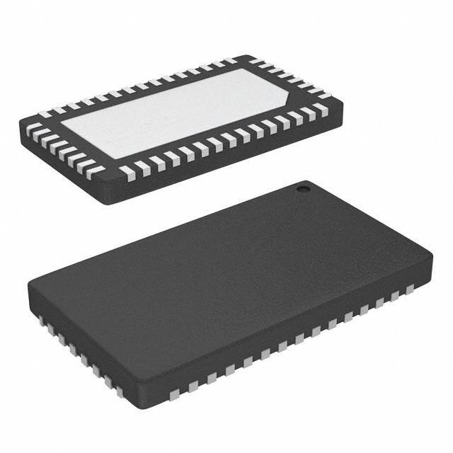
DATASHEET QLx4300-S45 FN6982 Quad Lane Extender Rev 1.00 November 19, 2009 The QLx4300-S45 is a settable quad receive-side Features equalizer with extended functionality for advanced • Supports data rates up to 3.125Gb/s protocols operating with line rates up to 3.125Gb/s such as InfiniBand (SDR) and 10GBase-CX4. The • Low power (78mW per channel) QLx4300-S45 compensates for the frequency • Low latency (<500ps) dependent attenuation of copper twin-axial cables, • Four equalizers in a 4mmx7mm QFN package for extending the signal reach up to 40m on 24AWG cable. straight route-through architecture and simplified The small form factor, highly-integrated quad design is routing ideal for high-density data transmission applications • Each equalizer boost is independently pin including active copper cable assemblies. The four selectable and programmable equalizing filters within the QLx4300-S45 can each be • Beacon signal support and line silence preservation set to one of 32 compensation levels, providing optimal signal fidelity for a given media and length. The • 1.2V supply voltage compensation level for each filter can be set by either (a) three external control pins or (b) a serial bus • Individual channel power-down (impedance select) interface. When the external control pins are used, 18 Applications of the 32 boost levels are available for each channel. If the serial bus is used, all 32 compensation levels are • InfiniBand (SDR) available. • 10GBase-CX4 Operating on a single 1.2V power supply, the • PCI Express (Gen 1) QLx4300-S45 enables per channel throughputs of up • DisplayPort to 3.125Gb/s while supporting the lower data rates of • XAUI 2.5Gb/s and 1.5Gb/s. The QLx4300-S45 uses current mode logic (CML) inputs/outputs and is packaged in a • SAS (1.0) 4mmx7mm 46 lead QFN. Individual lane impedance • High-speed active cable assemblies select support is included for module applications. • High-speed printed circuit board (PCB) traces Benefits • Thinner gauge cable • Extends cable reach greater than 3x • Improved BER Typical Application Circuit QLX4300-S45 QLX4300-S45 <40M 24AWG FN6982 Rev 1.00 Page 1 of 21 November 19, 2009
QLx4300-S45 Ordering Information PART NUMBER TEMP. RANGE PACKAGE (Note) PART MARKING (°C) (Pb-Free) PKG. DWG.# QLX4300SIQT7 QLX4300SIQ 0 to +70 46 Ld QFN L46.4x7 7” Prod. Tape & Reel; Qty 1,000 QLX4300SIQSR QLX4300SIQ 0 to +70 46 Ld QFN L46.4x7 7” Sample Reel; Qty 100 NOTE: These Intersil Pb-free plastic packaged products employ special Pb-free material sets; molding compounds/die attach materials and NiPdAu plate - e4 termination finish, which is RoHS compliant and compatible with both SnPb and Pb-free soldering operations. Intersil Pb-free products are MSL classified at Pb-free peak reflow temperatures that meet or exceed the Pb-free requirements of IPC/JEDEC J STD-020. Pin Configuration QLx4300-S45 (46 LD 4x7 QFN) TOP VIEW A] B] C] A] B] C] K B 1[ 1[ 1[ 2[ 2[ 2[ L N P P P P P P C E C C C C C C 46 45 44 43 42 41 40 39 DT 1 38 BGREF IN1[P] 2 37 OUT1[P] IN1[N] 3 36 OUT1[N] VDD 4 35 VDD IN2[P] 5 34 OUT2[P] IN2[N] 6 33 OUT2[N] VDD 7 32 VDD IN3[P] 8 EXPOSED PAD 31 OUT3[P] (GND) IN3[N] 9 30 OUT3[N] VDD 10 29 VDD IN4[P] 11 28 OUT4[P] IN4[N] 12 27 OUT4[N] IS1 13 26 IS3 IS2 14 25 IS4 GND 15 24 MODE 16 17 18 19 20 21 22 23 DI O A] B] C] A] B] C] D 3[ 3[ 3[ 4[ 4[ 4[ P P P P P P C C C C C C FN6982 Rev 1.00 Page 2 of 21 November 19, 2009
QLx4300-S45 Pin Descrptions PIN NAME PIN NUMBER DESCRIPTION DT 1 Detection Threshold. Reference DC current threshold for input signal power detection. Data output OUT[k] is muted when the power of the equalized version of IN[k] falls below the threshold. Tie to ground to disable electrical idle preservation and always enable the limiting amplifier. IN1[P,N] 2, 3 Equalizer 1 differential input, CML. The use of 100nF low ESL/ESR MLCC capacitor with at least 4GHz frequency response is recommended. VDD 4, 7, 10, 29, Power supply. 1.2V supply voltage. The use of parallel 100pF and 10nF decoupling capacitors to 32, 35 ground is recommended for each of these pins for broad high-frequency noise suppression. IN2[P,N] 5, 6 Equalizer 2 differential input, CML. The use of 100nF low ESL/ESR MLCC capacitor with at least 4GHz frequency response is recommended. IN3[P,N] 8, 9 Equalizer 3 differential input, CML. The use of 100nF low ESL/ESR MLCC capacitor with at least 4GHz frequency response is recommended. IN4[P,N] 11, 12 Equalizer 4 differential input, CML. The use of 100nF low ESL/ESR MLCC capacitor with at least 4GHz frequency response is recommended. IS1 13 Impedance Select 1. CMOS logic input. When the voltage on this pin is LOW, the single-ended input impedance of In1P and In1N each go above 200k and powers down the channel. This pin should be connected to the Fundamental Reset signal in PCI Express™. Otherwise, connect to VDD to hold the input impedance at 50. IS2 14 Impedance Select 2. CMOS logic input. When the voltage on this pin is LOW, the single-ended input impedance of In2P and In2N each go above 200k and powers down the channel. This pin should be connected to the Fundamental Reset signal in PCI Express™. Otherwise, connect to VDD to hold the input impedance at 50. GND 15 Ground DI 16 Serial data input, CMOS logic. Input for serial data stream to program internal registers controlling the boost for all four equalizers. Synchronized with clock (CLK) on pin 46. Overrides the boost setting established on CP control pins. Internally pulled down. DO 17 Serial data output, CMOS logic. Output of the internal registers controlling the boost for all four equalizers. Synchronized with clock on pin 46. Equivalent to serial data input on DI but delayed by 21 clock cycles. CP3[A,B,C] 18, 19, 20 Control pins for setting equalizer 3. CMOS logic inputs. Pins are read as a 3-digit number to set the boost level. A is the MSB, and C is the LSB. Pins are internally pulled down through a 25k resistor. CP4[A,B,C] 21, 22, 23 Control pins for setting equalizer 4. CMOS logic inputs. Pins are read as a 3-digit number to set the boost level. A is the MSB, and C is the LSB. Pins are internally pulled down through a 25k resistor. MODE 24 Boost-level control mode input, CMOS logic. Allows serial programming of internal registers through pins DI, ENB, and Clk when set HIGH. Resets all internal registers to zero and uses boost levels set by CP pins when set LOW. If serial programming is not used, this pin should be grounded. IS4 25 Impedance Select 4. CMOS logic input. When the voltage on this pin is LOW, the single-ended input impedance of In4P and In4N each go above 200k and powers down the channel. This pin should be connected to the Fundamental Reset signal in PCI Express™. Otherwise, connect to VDD to hold the input impedance at 50. IS3 26 Impedance Select 3. CMOS logic input. When the voltage on this pin is LOW, the single-ended input impedance of In3P and In3N each go above 200k and powers down the channel. This pin should be connected to the Fundamental Reset signal in PCI Express™. Otherwise, connect to VDD to hold the input impedance at 50. OUT4[N,P] 27, 28 Equalizer 4 differential output, CML. The use of 100nF low ESL/ESR MLCC capacitor with at least 4GHz frequency response is recommended. OUT3[N,P] 30, 31 Equalizer 3 differential output, CML. The use of 100nF low ESL/ESR MLCC capacitor with at least 4GHz frequency response is recommended. FN6982 Rev 1.00 Page 3 of 21 November 19, 2009
QLx4300-S45 Pin Descrptions (Continued) PIN NAME PIN NUMBER DESCRIPTION OUT2[N,P] 33, 34 Equalizer 2 differential output, CML. The use of 100nF low ESL/ESR MLCC capacitor with at least 4GHz frequency response is recommended. OUT1[N,P] 36, 37 Equalizer 1 differential output, CML. The use of 100nF low ESL/ESR MLCC capacitor with at least 4GHz frequency response is recommended. BGREF 38 External bandgap reference resistor. Recommended value of 6.04k ±1%. CP2[C,B,A] 39, 40, 41 Control pins for setting equalizer 2. CMOS logic inputs. Pins are read as a 3-digit number to set the boost level. A is the MSB, and C is the LSB. Pins are internally pulled down through a 25k resistor. CP1[C,B,A] 42, 43, 44 Control pins for setting equalizer 1. CMOS logic inputs. Pins are read as a 3-digit number to set the boost level. A is the MSB, and C is the LSB. Pins are internally pulled down through a 25k resistor. ENB 45 Serial data enable (active low), CMOS logic. Internal registers can be programmed with DI and CLK pins only when the ENB pin is ‘LOW’. Internally pulled down. CLK 46 Serial data clock, CMOS logic. Synchronous clock for serial data on DI and DO pins. Data on DI is latched on the rising clock edge. Clock speed is recommended to be between 10MHz and 20MHz. Internally pulled down. EXPOSED - Exposed ground pad. For proper electrical and thermal performance, this pad should be PAD connected to the PCB ground plane. FN6982 Rev 1.00 Page 4 of 21 November 19, 2009
QLx4300-S45 Absolute Maximum Ratings Thermal Information Supply Voltage (VDD to GND) . . . . . . . . . . . . -0.3V to 1.3V Thermal Resistance (Typical) JA (°C/W) Jc (°C/W) Voltage at All Input Pins . . . . . . . . . . . -0.3V to VDD + 0.3V 46 Ld QFN Package (Note 1). . . . . 32 2.3 ESD Rating at All Pins. . . . . . . . . . . . . . . . . . . . 2kV (HBM) Operating Ambient Temperature Range. . . . . . 0°C to +70°C Storage Ambient Temperature Range. . . . .-55°C to +150°C Maximum Junction Temperature. . . . . . . . . . . . . . . +125°C Pb-Free Reflow Profile. . . . . . . . . . . . . . . . . . see link below http://www.intersil.com/pbfree/Pb-FreeReflow.asp CAUTION: Do not operate at or near the maximum ratings listed for extended periods of time. Exposure to such conditions may adversely impact product reliability and result in failures not covered by warranty. NOTE: 1. JA is measured with the component mounted on a high effective thermal conductivity test board in free air. See Tech Brief TB379 for details. Operating Conditions PARAMETER SYMBOL CONDITION MIN TYP MAX UNITS Supply Voltage VDD 1.1 1.2 1.3 V Operating Ambient Temperature TA 0 25 70 °C Bit Rate NRZ data applied to any channel 1.5 3.125 Gb/s Control Pin Characteristics Typical values are at VDD = 1.2V, TA = +25°C, and VIN = 800mVP-P, unless otherwise noted. VDD = 1.1V to 1.3V, TA = 0°C to +70°C. PARAMETER SYMBOL CONDITION MIN TYP MAX UNITS NOTES Input ‘LOW’ Logic Level VIL DI, Clk, ENB 0 0 350 mV Input ‘HIGH’ Logic Level VIH DI, Clk, ENB 750 VDD mV Output ‘LOW’ Logic Level VOL IS[k], DO 0 0 250 mV Output ‘HIGH’ Logic Level VOH IS[k], DO 1000 VDD mV ‘LOW’ Resistance State CP[k][A,B,C] 0 1 k 2 ‘MID’ Resistance State CP[k][B,C] 22.5 25 27.5 k 2 ‘HIGH’ Resistance State CP[k][A,B,C] 500 k 2 Input Current Current draw on digital pin, i.e., 30 100 µA CP[k][A,B,C], DI, Clk, ENB NOTE: 2. If four CP pins are tied together, the resistance values in this table should be divided by four. Electrical Specifications Typical values are at VDD = 1.2V, TA = +25°C, and VIN = 800mVP-P, unless otherwise noted. VDD= 1.1V to 1.3V, TA = 0°C to +70°C. PARAMETERS SYMBOL CONDITION MIN TYP MAX UNITS NOTES Supply Current IDD 260 mA Cable Input Amplitude VIN Measured differentially at data source 800 1200 1600 mVP-P 3 Range before encountering channel loss DC Differential Input Measured on input channel IN[k] 80 100 120 Resistance DC Single-Ended Input Measured on input channel IN[k]P or 40 50 60 Resistance IN[k]N Input Return Loss SDD11 50MHz to 3.75GHz 10 dB 4 (Differential) Input Return Loss SCC11 50MHz to 3.75GHz 6 dB 4 (Common Mode) FN6982 Rev 1.00 Page 5 of 21 November 19, 2009
QLx4300-S45 Electrical Specifications Typical values are at VDD = 1.2V, TA = +25°C, and VIN = 800mVP-P, unless otherwise noted. VDD= 1.1V to 1.3V, TA = 0°C to +70°C. (Continued) PARAMETERS SYMBOL CONDITION MIN TYP MAX UNITS NOTES Input Return Loss SDC11 50MHz to 3.75GHz 20 dB 4 (Com.to Diff. Conversion) Output Amplitude Range VOUT Active data transmission mode; Measured 450 550 650 mVP-P differentially at OUT[k]P and OUT[k]N with 50 load on both output pins Line Silence mode; Measured differentially 10 20 mVP-P at OUT[k]P and OUT[k]N with 50 load on both output pins Differential Output Measured on OUT[k] 80 105 120 Impedance Output Return Loss SDD22 50MHz to 3.75GHz 10 dB 4 (Differential) Output Return Loss SCC22 50MHz to 3.75GHz 5 dB 4 (Common Mode) Output Return Loss (Com. SDC22 50MHz to 3.75GHz 20 dB 4 to Diff. Conversion) Output Residual Jitter 3.125Gb/s; Up to 20m 24AWG standard 0.15 0.25 UI 3, 5, 6 twin-axial cable (approx. -25dB @ 2.5GHz); 800mVP-P VIN 1600mVP-P Output Transition Time tr, tf 20% to 80% 30 60 80 ps 7 Lane-to-Lane Skew 50 ps Propagation Delay From IN[k] to OUT[k] 500 ps Data-to-Line Silence tDS Time to transition from active data to line 15 ns 8, 11 Response Time silence (muted output) on 20m 24AWG standard twin-axial cable at 3.125Gb/s Time from last bit of ALIGN(0) for SAS OOB 14 ns 12 signaling to line silence (<20mVP-P output); Meritec 24AWG 20m; 3.125Gb/s Line Silence-to-Data tSD Time to transition from line silence mode 20 ns 8, 11 Response Time (muted output) to active data on 20m 24AWG standard twin-axial cable at 3.125Gb/s Time from first bit of ALIGN(0) for SAS 19 ns 12 OOB signaling to 450mVP-P output; Meritec 24AWG 20m; 3.125Gb/s Timing Difference (SAS) |tDS - tSD| For SAS OOB signaling support; Meritec 5 ns 12 24AWG 20m NOTES: 3. After channel loss, differential amplitudes at QLx4300-S45 inputs must meet the input voltage range specified in “Absolute Maximum Ratings” on page5. 4. Temperature = +25°C, VDD = 1.2V. 5. Output residual jitter is the difference between the total jitter at the lane extender output and the total jitter of the transmitted signal (as measured at the input to the channel). Total jitter (TJ) is DJPP + 14.1 x RJRMS. 6. Measured using a PRBS 27-1 pattern. Deterministic jitter at the input to the lane extender is due to frequency-dependent, media-induced loss only. 7. Rise and fall times measured using a 1GHz clock with a 20ps edge rate. 8. For active data mode, cable input amplitude is 400mVP-P (differential) or greater. For line silence mode, cable input amplitude is 20mVP-P (differential) or less. 9. Measured differentially across the data source. FN6982 Rev 1.00 Page 6 of 21 November 19, 2009
QLx4300-S45 NOTES:(Continued) 10. During line silence, transmitter noise in excess of this voltage range may result in differential output amplitudes from the QLx4300-S45 that are greater than 20mVP-P. 11. The data pattern preceding line silence mode is comprised of the PCIe electrical idle ordered set (EIOS). The data pattern following line silence mode is comprised of the PCIe electrical idle exit sequence (EIES). 12. The data pattern preceding or following line silence mode is comprised of the SAS-2 ALIGN (0) sequence for OOB signaling at 3.125Gb/s, and amplitude of 800mVP-P. Serial Bus Timing Characteristics PARAMETER SYMBOL CONDITION MIN TYP MAX UNITS CLK Setup Time tSCK From the falling edge of ENB 10 ns DI Setup Time tSDI Prior to the rising edge of CLK 10 ns DI Hold Time tHDI From the rising edge of CLK 6 ns ENB ‘HIGH’ tHEN From the falling edge of the last data bit’s CLK 10 ns Boost Setting Operational tD From ENB ‘HIGH’ 10 ns DO Hold Time tCQ From the rising edge of CLK to DO transition 12 ns Clock Rate fCLK Reference clock for serial bus EQ programming 20 MHz Typical Performance Characteristics VDD = 1.2V, TA = +25°C, unless otherwise noted. Performance was characterized using the system testbed shown in Figure 1. Unless otherwise noted, the transmitter generated a non-return-to-zero (NRZ) PRBS-7 sequence at 800mVP-P (differential) with 10ps of peak-to-peak deterministic jitter. This transmit signal was launched into twin-axial cable test channels of varying gauges and lengths. The loss characteristics of these test channels are plotted as a function of frequency in Figure 2. The received signal at the output of these test channels was then processed by the QLx4300-S45 before being passed to a receiver. Eye diagram measurements were made with 4000 waveform acquisitions and include random jitter. SMA SMA Pattern 100O Twin-Axial QLx4300-S45 Adapter Adapter Oscilloscope Generator Cable Eval Board Card Card FIGURE 1. DEVICE CHARACTERIZATION TEST SETUP TEST CHANNEL LOSS CHARACTERISTICS 0 -5 -10 -15 B) d -20 1 ( -25 2 D D -30 10m S -35 15m -40 20m -45 25m -50 0 1 2 3 4 5 6 Frequency (GHz) FIGURE 2. 26 AWG TWIN-AXIAL CABLE LOSS AS A FUNCTION OF FREQUENCY FOR VARIOUS TEST CHANNELS FN6982 Rev 1.00 Page 7 of 21 November 19, 2009
QLx4300-S45 Typical Performance Characteristics (Continued) 0.35 0.3 0.25 s) p 0.2 r ( e Jitt 0.15 10m 0.1 15m 20m 0.05 25m 0 0 5 10 15 20 25 30 35 Boost Setting FIGURE 2. JITTER VS BOOST SETTING FOR VARIOUS CABLE LENGTHS, PRBS-7, 0.03PS SYSTEM JITTER INCLUDED OUTPUT EYE DIAGRAMS v v di di / / V V m m 0 0 6 8 64ps/div 64ps/div FIGURE 3. RECEIVED SIGNAL AFTER 10m OF 26AWG FIGURE 4. QLx4300-S45 OUTPUT AFTER 10m OF 26AWG TWIN-AXIAL CABLE, 3.125Gb/s TWIN-AXIAL CABLE, 3.125Gb/s v v di di / / V V m m 0 0 8 8 64ps/div 64ps/div FIGURE 5. RECEIVED SIGNAL AFTER 15m OF 26AWG FIGURE 6. QLx4300-S45 OUTPUT AFTER 15m OF 26AWG TWIN-AXIAL CABLE, 3.125Gb/s TWIN-AXIAL CABLE, 3.125Gb/s FN6982 Rev 1.00 Page 8 of 21 November 19, 2009
QLx4300-S45 Typical Performance Characteristics (Continued) v v di di / / V V m m 0 0 7 8 64ps/div 64ps/div FIGURE 7. RECEIVED SIGNAL AFTER 20m OF 26AWG FIGURE 8. QLx4300-S45 OUTPUT AFTER 20m OF 26AWG TWIN-AXIAL CABLE, 3.125Gb/s TWIN-AXIAL CABLE, 3.125Gb/s v v di di / / V V m m 0 0 6 6 64ps/div 64ps/div FIGURE 9. RECEIVED SIGNAL AFTER 25m OF 26AWG FIGURE 10. QLx4300-S45 OUTPUT AFTER 25m OF 26AWG TWIN-AXIAL CABLE, 3.125Gb/s TWIN-AXIAL CABLE, 3.125Gb/s RETURN LOSS AND CROSSTALK CHARACTERISTICS 0 0 Channel 1 Channel 1 -5 Channel 2 -5 Channel 2 Channel 3 Channel 3 B) -10 Channel 4 B) -10 Channel 4 d d 1 ( -15 2 ( -15 1 2 C C C C S -20 S -20 -25 -25 -30 -30 0 0.5 1 1.5 2 2.5 3 3.5 4 0 0.5 1 1.5 2 2.5 3 3.5 4 Frequency (GHz) Frequency (GHz) FIGURE 11. INPUT COMMON-MODE RETURN LOSS FIGURE 12. OUTPUT COMMON-MODE RETURN LOSS FN6982 Rev 1.00 Page 9 of 21 November 19, 2009
QLx4300-S45 Typical Performance Characteristics (Continued) 0 0 Channel 1 -5 -5 Channel 2 Channel 3 -10 -10 B) B) Channel 4 1 (d -15 2 (d -15 1 2 D -20 D -20 D D S Channel 1 S -25 -25 Channel 2 Channel 3 -30 -30 Channel 4 -35 -35 0 0.5 1 1.5 2 2.5 3 3.5 4 0 0.5 1 1.5 2 2.5 3 3.5 4 Frequency (GHz) Frequency (GHz) FIGURE 13. INPUT DIFFERENTIAL RETURN LOSS FIGURE 14. OUTPUT DIFFERENTIAL RETURN LOSS FIGURE 15. DIFFERENTIAL CROSSTALK BETWEEN FIGURE 16. DIFFERENTIAL CROSSTALK BETWEEN ADJACENT INPUT CHANNEL ADJACENT INPUT CHANNELS Operation equalizer is followed by a limiting amplification stage that provides a clean output signal with full amplitude swing The QLx4300-S45 is an advanced quad lane-extender for and fast rise-fall times for reliable signal decoding in a high-speed interconnects. A functional diagram of one of subsequent receiver. the four channels in the QLx4300-S45 is shown in Figure17. In addition to a robust equalization filter to IN[k] IS[k] SETTABLE LIMITING OUT[k] EQUILIZER AMPLIFIER compensate for channel loss and restore signal fidelity, the QLx4300-S45 contains unique integrated features to >200k BIT SELECT (CP[k]/DI) preserve special signaling protocols typically broken by other equalizers. The signal detect function is used to AMPLITUDE + MUTE mute the channel output when the equalized signal falls DETECTOR - ENABLED below the level determined by the Detection Threshold DT (DT) pin voltage. This function is intended to preserve FIGURE 17. FUNCTIONAL DIAGRAM OF A SINGLE periods of line silence (“quiescent state” in InfiniBand CHANNEL WITHIN THE QLx4300-S45 contexts). Individually Adjustable Equalization Boost As illustrated in Figure 17, the core of each high-speed Each channel in the QLx4300-S45 features an signal path in the QLx4300-S45 is a sophisticated independently settable equalizer for custom signal equalizer followed by a limiting amplifier. The equalizer restoration. Each equalizer can be set to one of 32 levels compensates for skin loss, dielectric loss, and impedance of compensation when the serial bus is used to program discontinuities in the transmission channel. Each FN6982 Rev 1.00 Page 10 of 21 November 19, 2009
QLx4300-S45 the boost level and one of 18 compensation levels when V the CP[k] pins are used to set the level. The equalizer DD transfer functions for a subset of these compensation levels are plotted in Figure 18. The flexibility of this IN[k] P adjustable compensation architecture enables signal fidelity to be optimized on a channel-by-channel basis, 50Ω providing support for a wide variety of channel characteristics and data rates ranging from 2.5Gb/s to 3.125Gb/s. Because the boost level is externally set Buffer rather than internally adapted, the QLx4300-S45 provides reliable communication from the very first bit transmitted. There is no time needed for adaptation and control loop convergence. Furthermore, there are no 50Ω pathological data patterns that will cause the IN[k] N QLx4300-S45 to move to an incorrect boost level. The “Applications Information” section beginning on page12 details how to set the boost level by both the FIGURE 19. CML INPUT EQUIVALENT CIRCUIT FOR THE CP-pin voltage approach and the serial programming QLx4300-S45 approach. V DD 52Ω 52Ω OUT[k] P OUT[k] N FIGURE 18. EQUALIZER TRANSFER FUNCTIONS FOR SETTINGS 0, 5, 10, 15, 20, 25, AND 31 IN FIGURE 20. CML OUTPUT EQUIVALENT CIRCUIT FOR THE QLx4300-S45 THE QLx4300-S45 NOTE: The load value of 52 is used to internally match CML Input and Output Buffers SDD22 for a characteristic impedance of 50. The input and output buffers for the high-speed data channels in the QLx4300-S45 are implemented using Line Silence/Electrical Idle/Quiescent Mode CML. Equivalent input and output circuits are shown in Line silence is commonly broken by the limiting Figures 19 and 20, respectively. amplification in other equalizers. This disruption can be detrimental in many systems that rely on line silence as part of the protocol. The QLx4300-S45 contains special lane management capabilities to detect and preserve periods of line silence while still providing the fidelity-enhancing benefits of limiting amplification during active data transmission. Line silence is detected by measuring the amplitude of the equalized signal and comparing that to a threshold set by the current at the DT pin. When the amplitude falls below the threshold, the output driver stages are muted and held at their nominal common mode voltage1. 1. The output common mode voltage remains constant during both active data transmission and output muting modes. FN6982 Rev 1.00 Page 11 of 21 November 19, 2009
QLx4300-S45 Channel Power-Down A] B] C] A] B] C] In addition to controlling the input impedance, the IS[k] LK NB P1[ P1[ P1[ P2[ P2[ P2[ C E C C C C C C pin powers down the equalizer channel when pulled low. 46 45 44 43 42 41 40 39 This feature allows a system controller individually to DT 1 38 BGREF power down unused channels and to minimize power IN1[P] 2 37 OUT1[P] consumption. Example: the signal to power down a IN1[N] 3 36 OUT1[N] channel could come from an Intelligent Platform Management controller in ATCA applications for E-Keying. VDD 4 35 VDD IN2[P] 5 34 OUT2[P] The current draw for a channel is reduced from 50mA to 3.8mA when powered down. IN2[N] 6 33 OUT2[N] VDD 7 32 VDD Applications Information IN3[P] 8 EXPOSED PAD 31 OUT3[P] (GND) IN3[N] 9 30 OUT3[N] Several aspects of the QLx4300-S45 are capable of being dynamically managed by a system controller to provide VDD 10 29 VDD maximum flexibility and optimum performance. These IN4[P] 11 28 OUT4[P] functions are controlled by interfacing to the highlighted IN43[N] 12 27 OUT4[N] pins in Figure 21. The specific procedures for controlling IS1 13 26 IS3 these aspects of the QLx4300-S45 are the focus of this IS2 14 25 IS4 section. GND 15 24 MODE 16 17 18 19 20 21 22 23 DI DO 3[A] 3[B] 3[C] 4[A] 4[B] 4[C] P P P P P P C C C C C C FIGURE 21. PIN DIAGRAM HIGHLIGHTING PINS USED FOR DYNAMIC CONTROL OF THE QLx4300-S45 TABLE 1. DESCRIPTIONS OF PINS THAT CAN BE USED TO SET EQUALIZATION BOOST LEVEL PIN PIN NAME NUMBER DESCRIPTION DI 16 Serial data input, CMOS logic. Input for serial data stream to program internal registers controlling the boost for all four equalizers. Synchronized with clock (CLK) on pin 46. Overrides the boost setting established on CP control pins. Internally pulled down. DO 17 Serial data output, CMOS logic. Output of the internal registers controlling the boost for all four equalizers. Synchronized with clock on pin 46. Equivalent to serial data input on DI but delayed by 21 clock cycles. CP3[A,B,C] 18, 19, 20 Control pins for setting equalizer 3. CMOS logic inputs. Pins are read as a 3-digit number to set the boost level. A is the MSB, and C is the LSB. Pins are internally pulled down through a 25k resistor. CP4[A,B,C] 21, 22, 23 Control pins for setting equalizer 4. CMOS logic inputs. Pins are read as a 3-digit number to set the boost level. A is the MSB, and C is the LSB. Pins are internally pulled down through a 25k resistor. MODE 24 Boost-level control mode input, CMOS logic. Allows serial programming of internal registers through pins DI, ENB, and Clk when set “HIGH”. Resets all internal registers to zero and uses boost levels set by CP pins when set LOW. If serial programming is not used, this pin should be grounded. CP2[C,B,A] 39, 40, 41 Control pins for setting equalizer 2. CMOS logic inputs. Pins are read as a 3-digit number to set the boost level. A is the MSB, and C is the LSB. Pins are internally pulled down through a 25k resistor. CP1[C,B,A] 42, 43, 44 Control pins for setting equalizer 1. CMOS logic inputs. Pins are read as a 3-digit number to set the boost level. A is the MSB, and C is the LSB. Pins are internally pulled down through a 25k resistor. ENB 45 Serial data enable (active low), CMOS logic. Internal registers can be programmed with DI and CLK pins only when the ENB pin is ‘LOW’. Internally pulled down. CLK 46 Serial data clock, CMOS logic. Synchronous clock for serial data on DI and DO pins. Data on DI is latched on the rising clock edge. Clock speed is recommended to be between 10MHz and 20MHz. Internally pulled down. FN6982 Rev 1.00 Page 12 of 21 November 19, 2009
QLx4300-S45 Equalization Boost Level TABLE 2. MAPPING BETWEEN CP-SETTING RESISTOR Channel equalization for the QLx4300-S45 can be AND PROGRAMMED BOOST LEVELS individually set to either (a) one of 18 levels through the RESISTANCE BETWEEN CP PIN AND VDD DC voltages on external control pins or (b) one of 32 SERIAL levels via a set of registers programmed by a low speed CP[A] CP[B] CP[C] BOOST LEVEL serial bus. The pins used to control the boost level are Open Open Open 0 highlighted in Figure 21. Descriptions of these pins are listed in Table 1. Please refer to “Pin Descrptions” on Open Open 25k 2 page3 for descriptions of all other pins on the Open Open 0 4 QLx4300-S45. Open 25k Open 6 The boost setting for equalizer channel k can be read as a three digit ternary number across CP[k][A,B,C]. The Open 25k 25k 8 ternary value is established by the value of the resistor Open 25k 0 10 between VDD and the CP[k][A,B,C] pin. Open 0 Open 12 As a second option, the equalizer boost setting can be Open 0 25k 14 taken from a set of registers programmed through a serial bus interface (pins 16, 17, 45, and 46). Using this Open 0 0 15 interface, a set of registers is programmed to store the 0 Open Open 16 boost level. A total of 21 registers are used. Registers 2 through 21 are parsed into four 5-bit words. Each 5-bit 0 Open 25k 17 word determines which of 32 boost levels to use for the 0 Open 0 19 corresponding equalizer. Register 1 instructs the QLx4300-S45 to use registers 2 through 21 to set the 0 25k Open 21 boost level rather than the control pins CP[k][A,B,C]. 0 25k 25k 23 Both options have their relative advantages. The control 0 25k 0 24 pin option minimizes the need for external controllers as 0 0 Open 26 the boost level can be set in the board design resulting in a compact layout. The register option is more flexible for 0 0 25k 28 cases in which the optimum boost level will not be known 0 0 0 31 and can be changed by a host bus adapter with a small number of pins. It is noted that the serial bus interface Control Pin Boost Setting can also be daisy-chained among multiple QLx4300-S45 devices to afford a compact programmable solution even When register 1 of the QLx4300-S45 is zero (the default when a large number of data lines need to be equalized. state on power-up), the voltages at the CP pins are used to determine the boost level of each channel. For each of Upon power-up, the default value of all the registers (and the four channels, k, the [A], [B], and [C] control pins register 1 in particular) is zero, and thus, the CP pins are (CP[k]) are associated with a 3-bit non binary word. used to set the boost level. This permits an alternate While [A] can take one of two values, ‘LOW’ or ‘HIGH’, interpretation on setting the boost level. Specifically, the [B] and [C] can take one of three different values: ‘LOW’, CP pins define the default boost level until the registers ‘MIDDLE’, or ‘HIGH’. This is achieved by changing the are (if ever) programmed via the serial bus. value of a resistor connected between VDD and the CP pin, which is internally pulled low with a 25k resistor. Thus, a ‘HIGH’ state is achieved by using a 0 resistor, ‘MIDDLE’ is achieved with a 25k resistor, and ‘LOW’ is achieved with an open resistance. Table 2 defines the mapping from the 3-bit CP word to the 18 out of 32 possible levels available via the serial interface. If all four channels are to use the same boost level, then a minimum number of board resistors can be realized by tying together like CP[k][A,B,C] pins across all channels k. For instance, all four CP[k][A] pins can be tied to the same resistor running to VDD. Consequently, only three resistors are needed to control the boost of all four channels. If the CP Pins are tied together and the 25k is used, the value changes to a 6.25k resistor because the 25k is divided by 4. FN6982 Rev 1.00 Page 13 of 21 November 19, 2009
QLx4300-S45 Optimal Cable Boost Settings TABLE 3. OPTIMAL CABLE BOOST SETTINGS The settable equalizing filter within the QLx4300-S45 APPROX. LOSS @ QLx4300-S45 enables the device to optimally compensate for CABLE 1.5625GHz (dB) BOOST frequency-dependent attenuation across a wide variety Cable A 17 12 of channels, data rates, and encoding schemes. For the reference channels plotted in Figure 2, Table 3 shows the Cable B 23 16 optimal boost setting when transmitting a PRBS-7 signal. Cable C 28 23 The optimal boost setting is defined as the equalizing filter setting that minimizes the output residual jitter of NOTE: Optimal boost settings should be determined on an the QLx4300-S45. The settings in Table 4 represent the application-by-application basis to account for variations in optimal settings for the QLx4300-S45 across an ambient channel type, loss characteristics, and encoding schemes. The temperature range of 0°C to +70°C. The optimal setting settings in this table are presented as guidelines to be used as a starting point for application-specific optimization. at room temperature (+20°C to +40°C) is generally one to two settings lower than the values listed in Table 3. Register Description The QLx4300-S45’s internal registers are listed in Table4. Register 1 determines whether the CP pins or register values 2 through 21 are used to set the boost level. When this register is set, the QLx4300-S45 uses registers 2-6, 7-11, 12-16, and 17-21 to set the boost level of equalizers 1, 2, 3, and 4. When register 1 is not set, the CP pins are used to determine the boost level for each equalizer channel. The use of five registers for each equalizer channel allows all 32 boost levels as candidate boost levels. TABLE 4. DESCRIPTION OF INTERNAL SERIAL REGISTERS EQUALIZER REGISTER CHANNEL DESCRIPTION 1 1-4 CP control override – Use registers 2 through 21 (rather than CP pins) to establish the boost levels when this bit is set. 2 1 Equalizer setting bit 0 (LSB). 3 Equalizer setting bit 1. 4 Equalizer setting bit 2. 5 Equalizer setting bit 3. 6 Equalizer setting bit 4 (MSB). 7 2 Equalizer setting bit 0 (LSB). 8 Equalizer setting bit 1. 9 Equalizer setting bit 2. 10 Equalizer setting bit 3. 11 Equalizer setting bit 4 (MSB). 12 3 Equalizer setting bit 0 (LSB). 13 Equalizer setting bit 1. 14 Equalizer setting bit 2. 15 Equalizer setting bit 3. 16 Equalizer setting bit 4 (MSB). 17 4 Equalizer setting bit 0 (LSB). 18 Equalizer setting bit 1. 19 Equalizer setting bit 2. 20 Equalizer setting bit 3. 21 Equalizer setting bit 4 (MSB). FN6982 Rev 1.00 Page 14 of 21 November 19, 2009
QLx4300-S45 ENB t t SCK HEN CLK t t SDI HDI DI R21 R20 R19 R1 FIGURE 22. TIMING DIAGRAM FOR PROGRAMMING THE INTERNAL REGISTERS OF THE QLx4300-S45 Serial Bus Programming uses a common ENB signal as the serial data is carried-over from one QLx4300-S45 to the next. Pins 16 (DI), 45 (ENB), and 46 (CLK) are used to program the registers inside the QLx4300-S45. Figure22 Separate ENB Signals shows an exemplary timing diagram for the signals on Multiple QLx4300-S45 devices can be programmed from these pins. The serial bus can be used to program a a common serial data stream as shown in Figure 23. single QLx4300-S45 according to the following steps: Here, each QLx4300-S45 is provided its own ENB signal, 1. The ENB pin is pulled ‘LOW’. and only one of these ENB signals is pulled ‘LOW’, and - While this pin is ‘LOW’, the data input on DI are hence accepting the register data one at a time. In this read into registers but not yet latched. situation, the programming of each equalizer follows the steps outlined in Figure 22. - A setup time of tSCK is needed between ENB going ‘LOW’ and the first rising clock edge. DI/DO Carryover 2. At least 21 values are read from DI on the rising The DO pin (pin 17) can be used to daisy-chain the serial edge of the CLK signal. bus among multiple QLx4300-S45 chips. The DO pin outputs the overflow data from the DI pin. Specifically, as - If more than 21 values are passed in, then only the data is pipelined into a QLx4300-S45, it proceeds last 21 values are kept in a FIFO fashion. according to the following flow. First, a bit goes into - The data on DI should start by sending the value shadow register 1. Then, with each clock cycle, it shifts destined for register 21 and finish by sending the over into subsequent higher numbered registers. After value destined for register 1. shifting into register 21, it is output on the DO pin on the - A range of clock frequencies can be used. A typical same clock cycle. Thus, the DO signal is equal to the DI rate is 10MHz. The clock should not exceed 20MHz. signal, but delayed by 20 clock cycles. The timing - Setup (tSDI) and hold (tHDI) times are needed diagram for the DO pin is shown in Figure 24 where the around the rising clock edge. first 20 bits output from the DO are indefinite and subsequent bits are the data fed into the DI pin. The 3. The ENB pin is pulled ‘HIGH’ and the contents of the delay between the rising clock edge and the data registers are latched and take effect. transition is tCQ. - After clocking in the last data bit, an additional tHEN should elapse before pulling the ENB signal A diagram for programming multiple QLx4300-S45s is ‘HIGH’. shown in Figure 25. It is noted that the board layout should ensure that the additional clock delay experienced - After completing these steps, the new values will between subsequent QLx4300-S45s should be no more affect within tD. than the minimum value of tCQ, i.e. 12ns. Programming Multiple QLx4300-S45 Devices The serial bus interface provides a simple means of setting the equalizer boost levels with a minimal amount of board circuitry. Many of the serial interface signals can be shared among the QLx4300-S45 devices on a board and two options are presented in this section. The first uses common clock and serial data signals along with separate ENB signals to select which QLx4300-S45 accepts the programmed changes. The second method FN6982 Rev 1.00 Page 15 of 21 November 19, 2009
QLx4300-S45 Serial Register Data QLx4300-S45 QLx4300-S45 QLx4300-S45 QLx4300-S45 (A) (B) (C) (D) ENB DI ENB DI ENB DI ENB DI CLK DO CLK DO CLK DO CLK DO Clock ENB (A) ENB (B) ENB (C) ENB (D) FIGURE 23. SERIAL BUS PROGRAMMING MULTIPLE QLx4300-S45 DEVICES USING SEPARATE ENB SIGNALS ENB 20 Clock Cycles 21st Rising Edge t SCK CLK t CQ First Bit from DI DO FIGURE 24. TIMING DIAGRAM FOR DI/DO CARRYOVER Serial Register Data QLx4300-S45 QLx4300-S45 QLx4300-S45 QLx4300-S45 (A) (B) (C) (D) ENB DI ENB DI ENB DI ENB DI CLK DO CLK DO CLK DO CLK DO Clock ENB FIGURE 25. SERIAL BUS PROGRAMMING MULTIPLE QLx4300-S45 DEVICES USING DI/DO CARRYOVER FN6982 Rev 1.00 Page 16 of 21 November 19, 2009
QLx4300-S45 ENB t t SCK HEN CLK t t SDI HDI DI R21 R20 R1 R21 R1 R21 R1 R21 R1 QLx4300-S45 (D) QLx4300-S45 (C) QLx4300-S45 (B) QLx4300-S45 (A) FIGURE 26. TIMING DIAGRAM FOR PROGRAMMING MULTIPLE QLx4300-S45 DEVICES USING DI/DO CARRYOVER Detection Thereshold (DT) Pin Functionality The QLx4300-S45 is capable of maintaining periods of line silence on any of its four channels by monitoring each channel for loss of signal (LOS) conditions and subsequently muting the outputs of a respective channel when such a condition is detected. A reference current applied to the detection threshold (DT) pin is used to set the LOS threshold of the internal signal detection circuitry. Current control on the DT pin is done via one or two external resistors. Nominally, both a pull-up and pull-down resistor are tied to the DT pin (Figure 27A), FIGURE 27A. but if adequate control of the supply voltage is maintained to within ±3% of 1.2V, then a simple pull down resistor is adequate (as in Figure 27B). Resistors used should be at least 1/16W, with ±1% precision. The internal bias point of the DT pin, nominally 1.05V, is used in conjunction with the voltage divider (R1 and R2) shown in Figure 27A to set the reference current on the DT pin. Case 1: Channels with less than or equal to 17dB loss at 1.5625GHz: For signals transmitted on channels having less than or equal to 25dB of loss at 2.5GHz, the optimal DT FIGURE 27B. reference current is 0µA. This optimal reference current may be achieved by either leaving the DT pin floating, or tying the DT pin to ground (GND) with a 10M resistor. Case 2: Channels with greater 17dB loss at 1.5625GHz: For channels exhibiting more than 25dB of total loss (this includes cable or FR-4 loss) the DT pin should be configured for a reference sink current (coming out of the DT pin) of approximately 2µA. A typical configuration for a 2µA sink current is given in Figure 27C. If the configuration in Figure 27B is utilized, a 525k resistor is used. FIGURE 27C. FIGURE 27. FN6982 Rev 1.00 Page 17 of 21 November 19, 2009
QLx4300-S45 Typical Application Reference Designs Figures 28 and 29 show reference design schematics for a QLx4300-S45 evaluation board with an SMA connector interface. Figure 28 shows the schematic for the case when the equalizer boost level is set via the CP pins. Figure 29 shows the schematic for the case when the level is set via the serial bus interface. 1.2V 2k Detection threshold EQ Boost Control 2. reference current for Channels 1 and 2 4 (See pages 15-17) C C 6kO N N F k 7n 00 A] B] C] A] B] C] 4 1 K B 1[ 1[ 1[ 2[ 2[ 2[ L N P P P P P P C E C C C C C C 6 5 4 3 2 1 0 9 DT 4 4 4 4 4 4 4 3 BGREF A 1 38 IN1[P] OUT1[P] 2 37 IN1[N] OUT1[N] 3 36 1.2V 1.2V 4 35 IN2[P] 5 QLx4300-S45 34 OUT2[P] IN2[N] OUT2[N] 6 33 1.2V 1.2V 7 32 IN3[P] OUT3[P] 8 31 IN3[N] OUT3[N] 9 30 1.2V 1.2V 10 29 IN4[P] OUT4[P] 11 28 IN4[N] OUT4[N] 12 27 IS1 IS3 13 26 IS2 IS4 14 25 Impedance Select (Channels 1 and 2) GND MMOODDEE Impedance Select (Channels 3 and 4) 15 24 6 7 8 9 0 1 2 3 1 1 1 1 2 2 2 2 MODE at 1.2V: Serial Control Mode DI O A] B] C] A] B] C] MODE at GND: Binary Control Mode D 3[ 3[ 3[ 4[ 4[ 4[ P P P P P P C C C C C C 1.2V QLx4300-S45 C C N N EQ Boost Control LANE EXTENDER F F* for Channels 3 and 4 0n 0p (See pages 15-17) Reference 1 0 1 Control Pin Mode = SMA Connector Bypass circuit for each VDD pin: 4, 7, 10, 29, 32, 35 A) DC Blocking Capacitors = X7R or COG Quellan, Inc. (*100pF capacitor should be positioned closest to the pin) 0.1µF (>4GHz bandwidth) FIGURE 28. APPLICATION CIRCUIT FOR THE QLx4300-S45 EVALUATION BOARD USING THE CONTROL PINS FOR SETTING THE EQUALIZER COMPENSATION LEVEL FN6982 Rev 1.00 Page 18 of 21 November 19, 2009
QLx4300-S45 Typical Application Reference Designs (Continued) Figures 28 and 29 show reference design schematics for a QLx4300-S45 evaluation board with an SMA connector interface. Figure 28 shows the schematic for the case when the equalizer boost level is set via the CP pins. Figure 29 shows the schematic for the case when the level is set via the serial bus interface. w 1.2V o L 42.2k Dreetfeecretinocne t hcruersrehnotld erial Clock In nable Active NC 6kO S E nF 0k A] B] C] A] B] C] 47 10 LK NB P1[ P1[ P1[ P2[ P2[ P2[ C E C C C C C C 6 5 4 3 2 1 0 9 DT 4 4 4 4 4 4 4 3 BGREF A 1 38 IN1[P] OUT1[P] 2 37 IN1[N] OUT1[N] 3 36 1.2V 1.2V 4 35 IN2[P] 5 QLx4300-S45 34 OUT2[P] IN2[N] OUT2[N] 6 33 1.2V 1.2V 7 32 IN3[P] OUT3[P] 8 31 IN3[N] OUT3[N] 9 30 1.2V 1.2V 10 29 IN4[P] OUT4[P] 11 28 IN4[N] OUT4[N] 12 27 IS1 IS3 13 26 IS2 IS4 14 25 Impedance Select (Channels 1 and 2) GND MODE Impedance Select (Channels 3 and 4) 15 24 6 7 8 9 0 1 2 3 1 1 1 1 2 2 2 2 MODE at 1.2V: Serial Control Mode DI O A] B] C] A] B] C] MODE at GND: Binary Control Mode D 3[ 3[ 3[ 4[ 4[ 4[ P P P P P P C C C C C C 1.2V QLx4300-S45 a In Out NC F F* Dat ata LANE EXTENDER 10n 100p Serial erial D SeriaRl Cefoenretrnocl eMode S = SMA Connector Bypass circuit for each VDD pin: 4, 7, 10, 29, 32, 35 A) DC Blocking Capacitors = X7R or COG Quellan, Inc. (*100pF capacitor should be positioned closest to the pin) 0.1µF (>4GHz bandwidth) FIGURE 29. APPLICATION CIRCUIT FOR THE QLx4300-S45 EVALUATION BOARD USING THE SERIAL BUS INTERFACE FOR SETTING THE EQUALIZER COMPENSATION LEVEL FN6982 Rev 1.00 Page 19 of 21 November 19, 2009
QLx4300-S45 ® About Q:ACTIVE Intersil has long realized that to enable the complex server clusters of next generation datacenters, it is critical to manage the signal integrity issues of electrical interconnects. To address this, Intersil has developed its groundbreaking Q:ACTIVE® product line. By integrating its analog ICs inside cabling interconnects, Intersil is able to achieve unsurpassed improvements in reach, power consumption, latency, and cable gauge size as well as increased airflow in tomorrow’s datacenters. This new technology transforms passive cabling into intelligent “roadways” that yield lower operating expenses and capital expenditures for the expanding datacenter. Intersil Lane Extenders allow greater reach over existing cabling while reducing the need for thicker cables. This significantly reduces cable weight and clutter, increases airflow, and reduces power consumption. © Copyright Intersil Americas LLC 2009. All Rights Reserved. All trademarks and registered trademarks are the property of their respective owners. For additional products, see www.intersil.com/en/products.html Intersil products are manufactured, assembled and tested utilizing ISO9001 quality systems as noted in the quality certifications found at www.intersil.com/en/support/qualandreliability.html Intersil products are sold by description only. Intersil may modify the circuit design and/or specifications of products at any time without notice, provided that such modification does not, in Intersil's sole judgment, affect the form, fit or function of the product. Accordingly, the reader is cautioned to verify that datasheets are current before placing orders. Information furnished by Intersil is believed to be accurate and reliable. However, no responsibility is assumed by Intersil or its subsidiaries for its use; nor for any infringements of patents or other rights of third parties which may result from its use. No license is granted by implication or otherwise under any patent or patent rights of Intersil or its subsidiaries. For information regarding Intersil Corporation and its products, see www.intersil.com FN6982 Rev 1.00 Page 20 of 21 November 19, 2009
QLx4300-S45 Package Outline Drawing L46.4x7 46 LEAD THIN QUAD FLAT NO-LEAD PLASTIC PACKAGE (TQFN) Rev 0, 9/09 2.80 4.00 A 42X0.40 6 B 39 46 PIN 1 INDEX AREA 6 38 1 PIN 1 INDEX AREA 0 5.50 ±0.1 7.0 5.60 Exp. DAP 24 15 (4X) 0.05 46X 0.20 4 23 16 0.10MCAB TOP VIEW SIDE VIEW 2.50 ±0.1 46X 0.40 Exp. DAP BOTTOM VIEW SEE DETAIL "X" 0.10 C C 0.70 ±0.05 SEATING PLANE 0.05C SIDE VIEW C 0.152 REF 5 0 . 00 MIN. 0 . 05 MAX. DETAIL "X" ( 3.80 ) ( 2.50) NOTES: 1. Dimensions are in millimeters. Dimensions in ( ) for Reference Only. 2. Dimensioning and tolerancing conform to AMSE Y14.5m-1994. ( 6.80 ) ( 42X 0.40) 3. Unless otherwise specified, tolerance : Decimal ± 0.05 ( 5.50 ) 4. Dimension applies to the metallized terminal and is measured between 0.15mm and 0.30mm from the terminal tip. 5. Tiebar shown (if present) is a non-functional feature. (46X 0.20) 6. The configuration of the pin #1 identifier is optional, but must be located within the zone indicated. The pin #1 identifier may be either a mold or mark feature. ( 46 X 0.60) TYPICAL RECOMMENDED LAND PATTERN FN6982 Rev 1.00 Page 21 of 21 November 19, 2009