ICGOO在线商城 > 集成电路(IC) > PMIC - 电压基准 > ZXRE252BSA-7

 Datasheet下载
- 型号: ZXRE252BSA-7
- 制造商: Diodes Inc.
- 库位|库存: xxxx|xxxx
- 要求:
| 数量阶梯 | 香港交货 | 国内含税 |
| +xxxx | $xxxx | ¥xxxx |
查看当月历史价格
查看今年历史价格
ZXRE252BSA-7产品简介:
ICGOO电子元器件商城为您提供ZXRE252BSA-7由Diodes Inc.设计生产,在icgoo商城现货销售,并且可以通过原厂、代理商等渠道进行代购。 ZXRE252BSA-7价格参考。Diodes Inc.ZXRE252BSA-7封装/规格:PMIC - 电压基准, 分流器 电压基准 IC 36V ±0.5% 100mA SOT-23。您可以下载ZXRE252BSA-7参考资料、Datasheet数据手册功能说明书,资料中有ZXRE252BSA-7 详细功能的应用电路图电压和使用方法及教程。
Diodes Incorporated的ZXRE252BSA-7是一款精密电压基准芯片,属于PMIC(电源管理集成电路)中的电压基准类别。该器件提供高精度、低温度漂移的基准电压,适用于对电压稳定性要求较高的电子系统中。

其典型应用场景包括:

1. 模拟-数字转换系统(ADC/DAC):作为参考电压源,为ADC或DAC提供稳定的比较基准,确保转换精度。

2. 电源管理系统:在电池供电设备中,用于监测电池电压或提供稳定的系统基准,以实现精确的电源管理。

3. 工业控制系统:如传感器信号调理电路中,提供高精度参考电压,提高测量准确性。

4. 测试与测量设备:用于万用表、示波器等精密仪器中,确保测量结果的稳定性与重复性。

5. 通信设备:在基站、光模块等通信系统中,作为参考源用于电压监控和校准。

ZXRE252BSA-7采用SOT23-3封装,体积小、功耗低,适合便携式和空间受限的应用。其高精度和稳定性使其在需要可靠电压基准的各类电子设备中广泛使用。
| 参数 | 数值 |
| 产品目录 | 集成电路 (IC)半导体 |
| 描述 | IC VREF SHUNT PREC ADJ SOT23参考电压 Shunt Regulator |
| 产品分类 | |
| 品牌 | Diodes Incorporated |
| 产品手册 | |
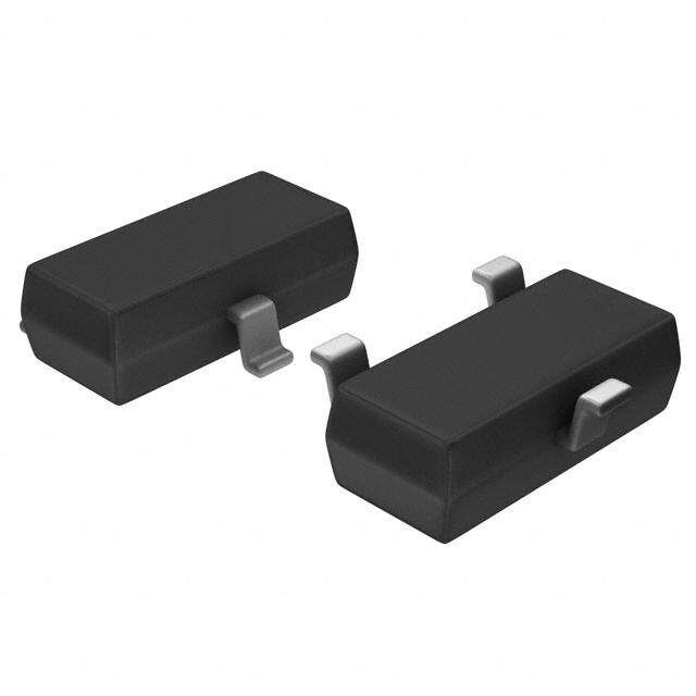
| 产品图片 |
|
| rohs | 符合RoHS无铅 / 符合限制有害物质指令(RoHS)规范要求 |
| 产品系列 | 电源管理 IC,参考电压,Diodes Incorporated ZXRE252BSA-7- |
| 数据手册 | |
| 产品型号 | ZXRE252BSA-7 |
| RoHS指令信息 | http://diodes.com/download/4349 |
| 串联VREF—电源电流—最大值 | - 0.05 mA to + 10 mA |
| 串联VREF—输入电压—最大值 | 2.507 V |
| 串联VREF—输入电压—最小值 | 2.482 V |
| 产品种类 | 参考电压 |
| 供应商器件封装 | SOT-23 |
| 其它名称 | ZXRE252BSA-7DIDKR |
| 分流电流—最大值 | 100 mA |
| 分流电流—最小值 | 0.065 mA |
| 初始准确度 | 0.5 % |
| 包装 | Digi-Reel® |
| 参考类型 | Shunt Adjustable Precision References |
| 商标 | Diodes Incorporated |
| 安装类型 | 表面贴装 |
| 安装风格 | SMD/SMT |
| 容差 | ±0.5% |
| 封装 | Reel |
| 封装/外壳 | TO-236-3,SC-59,SOT-23-3 |
| 封装/箱体 | SOT-23 |
| 工作温度 | -40°C ~ 125°C |
| 最大工作温度 | + 125 C |
| 最小工作温度 | - 40 C |
| 标准包装 | 1 |
| 温度系数 | - |
| 电压-输入 | - |
| 电压-输出 | 2.5 V ~ 36 V |
| 电流-输出 | 100mA |
| 电流-阴极 | 65µA |
| 电流-静态 | - |
| 输入电压 | 2.495 V |
| 输出电压 | 2.5 V to 36 V |
| 通道数 | 1 |


- 商务部:美国ITC正式对集成电路等产品启动337调查
- 曝三星4nm工艺存在良率问题 高通将骁龙8 Gen1或转产台积电
- 太阳诱电将投资9.5亿元在常州建新厂生产MLCC 预计2023年完工
- 英特尔发布欧洲新工厂建设计划 深化IDM 2.0 战略
- 台积电先进制程称霸业界 有大客户加持明年业绩稳了
- 达到5530亿美元!SIA预计今年全球半导体销售额将创下新高
- 英特尔拟将自动驾驶子公司Mobileye上市 估值或超500亿美元
- 三星加码芯片和SET,合并消费电子和移动部门,撤换高东真等 CEO
- 三星电子宣布重大人事变动 还合并消费电子和移动部门
- 海关总署:前11个月进口集成电路产品价值2.52万亿元 增长14.8%


PDF Datasheet 数据手册内容提取
NOT RECOMMENDED FOR NEW DESIGN USE AP431SHA(B)N1TR-G1 FOR ZXRE250B(A)SA-7 USE AP431SHA(B)NTR-G1FOR ZXRE252B(A)SA-7 ZXRE250 / ZXRE252 VERY LOW CATHODE CURRENT ADJUSTABLE PRECISION SHUNT REGULATOR Description Pin Assignments The ZXRE250 and ZXRE252 are three-terminal adjustable shunt ZXRE250 regulators that offer excellent temperature stability and output current ((TToopp VViieeww)) handling capability up to 100mA. The output voltage may be set to any chosen voltage between 2.5V and 36V by selection of two external divider resistors. 33 RREEFF AANNOODDEE 11 ZXRE250 has the same electrical specifications as the industry standard ‘431 except it features a very-low minimum cathode current 22 CCAATTHHOODDEE for regulation. The typical value of 40µA makes the parts ideal for very low-power applications. SSOOTT2233 The devices can be used as a replacement for zener diodes in many applications requiring an improvement in zener performance. The ((TToopp VV iieeww)) ZXRE250/2 is available in two grades with initial tolerances of 1% and 0.5% for the A and B grades respectively. NNCC 11 55 AANNOODDEE LLeeaavvee ffllooaattiinngg oorr 22 ccoonnnneecctt ttoo ppiinn 55 Features • Minimum Cathode Current for Regulation: 40μA (typ) CCAATTHHOODDEE 33 44 RREEFF • Temperature Range: -40°C to +125°C • Reference Voltage Tolerance at +25°C SSOOTT 2255 ZXRE250A: 2.495V ± 1.0% ZXRE250B: 2.495V ± 0.5% ZXRE252 • Low Output Noise • 0.2Ω Typical Output Impedance ((TToopp VV ii ee ww)) • Sink Current Capability: 0.065mA to 100mA • Adjustable Output Voltage: VREF to 36V 33 CCAATTHHOODDEE • Totally Lead-Free & Fully RoHS Compliant (Notes 1 & 2) • Halogen and Antimony Free. “Green” Device (Note 3) AANNOODDEE 11 22 RREEFF Applications • Optocoupler Linearisers SSOOTT 2233 • Shunt Regulators • Improved Zener • Variable Reference Notes: 1. No purposely added lead. Fully EU Directive 2002/95/EC (RoHS), 2011/65/EU (RoHS 2) & 2015/863/EU (RoHS 3) compliant. 2. See https://www.diodes.com/quality/lead-free/ for more information about Diodes Incorporated’s definitions of Halogen- and Antimony-free, "Green" and Lead-free. 3. Halogen- and Antimony-free "Green” products are defined as those which contain <900ppm bromine, <900ppm chlorine (<1500ppm total Br + Cl) and <1000ppm antimony compounds. ZXRE250 / ZXRE252 1 of 12 June 2018 Document number: DS35228 Rev. 7 - 3 www.diodes.com © Diodes Incorporated
ZXRE250 / ZXRE252 Absolute Maximum Ratings (Note 4) (@TA = +25°C, unless otherwise specified.) Symbol Parameter Rating Unit VKA Cathode Voltage 40 V IKA Continuous Cathode Current 150 mA IREF Reference Input Current -0.050 to +10 mA TJ Operating Junction Temperature +150 °C TST Storage Temperature -55 to +150 °C SOT23 330 mW PD Power Dissipation (Notes 5 & 6) SOT25 500 mW Notes: 4. Operation above the absolute maximum rating may cause device failure. Operation at the absolute maximum ratings, for extended periods, may reduce device reliability. Unless otherwise stated voltages specified are relative to the ANODE pin. 5. TJ, max = +150°C 6. Ratings apply to ambient temperature at +25°C. Recommended Operating Conditions (@TA = +25°C, unless otherwise specified.) Symbol Parameter Min Max Unit VKA Cathode Voltage VREF 36 V IKA Cathode Current 0.065 100 mA TA Operating Ambient Temperature -40 +125 °C Electrical Characteristics (@TA = +25°C, unless otherwise specified.) Symbol Parameter Test Conditions Min Typ Max Unit VREF Reference Voltage VKA = VREF, ZXRE250A 2.470 2.495 2.520 V IKA = 10mA ZXRE250B 2.482 2.495 2.507 V TA = 0 to +70°C — 6 16 mV VDEV DTeemviapteiorant uorfe R Reafenrgeen c(Ne oVtoel t7a)g e Over Full IVKKAA = = 1 V0RmEAF, TA = -40 to +85°C — 14 34 mV TA = -40 to +125°C — 14 34 mV ΔVREF Ratio of the Change in Reference VKA = 10V to VREF — -1.4 -2.7 mV/V ΔVKA VVoollttaaggee to the Change in Cathode IKA = 10mA VKA = 36V to 10V — -1 -2 mV/V IREF Reference Input Current IKA = 10mA, R1 = 10KΩ, R2 = ∞ — 1 4 µA TA = 0 to +70°C — 0.8 1.2 µA ΔIREF IRRaEFn Dgee v(Niaotitoen 7 O) ver Full Temperature I1K0AK =Ω 1, 0Rm2A =, R∞1 = TA = -40 to +85°C — 0.8 2.5 µA TA = -40 to +125°C — 0.8 2.5 µA IKA(MIN) Minimum Cathode Current for Regulation VKA = VREF — 40 65 µA IKA(OFF) Off-State Current VKA = 36V, VREF = 0V — 0.05 0.5 µA |ZKA| Dynamic Output Impedance (Note 8) VKA = VREF, f = 0Hz — 0.2 0.5 Ω SOT23 — 380 — °C/W ϴJA Thermal Resistance Junction to Ambient SOT25 — 250 — °C/W Notes: 7. Deviation of VDEV, and ΔIREF are defined as the maximum variation of the values over the full temperature range. 8. Derivation of ZKA on following page. ZXRE250 / ZXRE252 2 of 12 June 2018 Document number: DS35228 Rev. 7 - 3 www.diodes.com © Diodes Incorporated
ZXRE250 / ZXRE252 Electrical Characteristics (continued) (@TA = +25°C, unless otherwise specified.) The average temperature coefficient of the reference input voltage αVREF is defined as: VVmmaaxx VV DDEEVV XX 110066 VV @@ 2255ººCC ααVV == RREEFF ppppmm//ººCC RREEFF TT22 ––TT11 VVmmiinn Where: T2 - T1 = full temperature change. αVREF can be positive or negative depending on whether the slope is VVDDEEVV== VVmmaaxx--VVmmiinn positive or negative. Note : 8. The dynamic output impedance, RZ, is defined as: ΔΔVV ZZKKAA == ΔΔIIKKAA TT11 TTeemmppeerraattuurree TT22 KKAA When the device is programmed with two external resistors R1 and R2, the dynamic output impedance of the overall circuit, is defined as: ΔΔΔVVV RRR111 ZZZ’’’ === ΔΔΔIII ≈≈ ZZZKKKAAA 111 +++ RRR222 Test Circuits Figure 2 Test Circuit for VKA > VREF Figure 1 Test Circuit for VKA = VREF Figure 3 Test Circuit for IOFF ZXRE250 / ZXRE252 3 of 12 June 2018 Document number: DS35228 Rev. 7 - 3 www.diodes.com © Diodes Incorporated
ZXRE250 / ZXRE252 Typical Performance Characteristics 2600 0.2 2580 IVKKAA = = 1 V0RmEAF RR12 == 1∞0KΩ V) 2560 TA = 25°C ) IKA = 10mA m µA 0.15 ge ( 2540 nt ( a e olt 2520 urr V C ce 2500 ce 0.1 n n e e er 2480 er ef ef R R REF 2460 REF 0.05 V I 2440 2420 2400 0 -55 -35 -15 5 25 45 65 85 105 125 -55 -35 -15 5 25 45 65 85 105 125 TA Free Air Temperature (°C) TA Free Air Temperature (°C) Reference Voltage vs. Free Air Temperature Reference Current vs. Free Air Temperature 150 200 VTAKA = = 2 5V°RCEF VTAKA = = 2 5V°RCEF 100 ) ) A A µ ent (m 50 rrent (100 IKMIN urr Cu C e e d d o ho 0 ath at C 0 C A KA IK I -50 -100 -100 -2 -1 0 1 2 3 -2 -1 0 1 2 3 VKA Cathode Voltage (V) VKA Cathode Voltage Cathode Current vs. Cathode Voltage Cathode Current vs. Cathode Voltage 0.50 -0.2 VKA = 36V VKA = 3V to 36V 0.45 VREF = 0 -0.3 A) µ 0.40 nt ( -0.4 Cathode Curre 000...233550 /dV (mV/V)FKA --00..56 State 0.20 dVRE -0.7 Off- 0.15 -0.8 F F 0.10 O -0.9 K I 0.05 -1.0 -50 -25 0 25 50 75 100 125 0.00 -75 -50 -25 0 25 50 75 100 125 TA Free Air Temperature (C) T Free Air Temperature (°C) Ratio of Delta Reference Voltage to Delta Cathode A Off-State Cathode Current vs. Free Air Temperature Voltage vs. Free Air Temperature ZXRE250 / ZXRE252 4 of 12 June 2018 Document number: DS35228 Rev. 7 - 3 www.diodes.com © Diodes Incorporated
ZXRE250 / ZXRE252 Typical Performance Characteristics (Continued) 400 15 √e nV/Hz 336800 IVTKAKAA == = 21 5V0°RmCEAF µe - V 10 IVTKAKAA == = 21 5V0°RmCEAF g g Volta 340 Volta 5 se 320 se oi oi N N ut 300 ut 0 p p n n nt I 280 nt I e e -5 al 260 al v v ui ui q q E 240 E V = N220 Vn - -10 200 -15 10 100 1K 10K 100K 0 1 2 3 4 5 6 7 8 9 10 f- Frequency (Hz) Time (Seconds) Equivalent Input Noise Voltage vs. Frequency Equivalent Input Noise Voltage Over A 10-S Period Figure 4 Test Circuit for Noise Input Voltage ZXRE250 / ZXRE252 5 of 12 June 2018 Document number: DS35228 Rev. 7 - 3 www.diodes.com © Diodes Incorporated
ZXRE250 / ZXRE252 Typical Performance Characteristics (Cont.) 70 n (dB) 60 ITKAA == 2150°mCA o ati mplific 50 A e 40 g a olt V 30 al n g Si 20 all- m S V10 A Test Circuit for Voltage Amplification 0 100 1K 10K 100K 1M 10M f Frequency (Hz) Small-Signal Voltage Amplification vs. Frequency 100.0 IKA = 10mA TA = 25°C Ω) ( e 10.0 nc da pe m e I 1.0 c n e er ef R A ZK 0.1 Test Circuit for Reference Impedance 0.0 1K 10K 100K 1M 10M f Frequency (Hz) Reference Impedance vs. Frequency ZXRE250 / ZXRE252 6 of 12 June 2018 Document number: DS35228 Rev. 7 - 3 www.diodes.com © Diodes Incorporated
ZXRE250 / ZXRE252 Typical Performance Characteristics (Cont.) 6 Input TA = 25°C 5 ) V ( e g a 4 olt V ut p ut 3 Output O d n ut a 2 p n I Test Circuit for Pulse Response 1 0 0 1 2 3 4 5 6 7 8 9 10 t Time (µs) Pulse Response 100 D D TA = 25°C 90 80 mA C C A B nt - 70 Stable Stable Stable urre 60 C e 50 B d o Test Circuit for Curve A h at 40 C - KA 30 I 20 A VKA = VREF B VKA = 5V 10 CD VVKKAA == 1105VV 0 0.00001 0.0001 0.001 0.01 0.1 1 10 C -Load Capacitance - uF L Stability Boundary Conditions Test Circuit for Curves B, C, D The device is stable under all conditions with a load capacitance not exceeding 50pF. The device is stable under all conditions with a load capacitance between 5nF and 20nF. The device is stable under all conditions with a load capacitance exceeding 300nF. With a cathode current not exceeding 5mA, the device is stable with any load capacitance. ZXRE250 / ZXRE252 7 of 12 June 2018 Document number: DS35228 Rev. 7 - 3 www.diodes.com © Diodes Incorporated
ZXRE250 / ZXRE252 Application Information V+ V V+ V OUT OUT R1 R1 V V REF REF R2 R2 VOUT=(1+RR12)VREF VOUT=(1+RR12)VREF Higher Current Shunt Regulator Shunt Regulator V+ ZSR*** V+ In Out VOUT 30Ω Common R1 0.01µF Rb V REF R1 V R2 OUT V REF R2 V =V +V OUT(min) REF REG VOUT=(1+RR12)VREF Rb - Optional to provide minimum cathode current VOUT=(1+RR12)VREF Output Control of a Three Series Regulator Terminal Fixed Regulator V+ V+ R1B R1A V REF Output Output VREF Input VON~~2V R2A R2B VTH= 2.5V VOFF=V+ Low Limit=(1+R1B)V R2B REF High Limit=(1+R1A)V Single Supply Comparator R2A REF with Temperature Over Voltage / Under Compensated Threshold Voltage Protection Circuit ZXRE250 / ZXRE252 8 of 12 June 2018 Document number: DS35228 Rev. 7 - 3 www.diodes.com © Diodes Incorporated
ZXRE250 / ZXRE252 Ordering Information ZXRE25XXXX-7 Pinout variation Tolerance Package Packing 0: Standard pinout A:±1.0% SA: SOT23 7: Tape & Reel 2: Reversed pinout in SOT23 B:± 0.5% W5: SOT25 Part Number Package 7” Tape and Reel Ammo Box Packaging (Note 9) Code Quantity Part Number Suffix Quantity Part Number Suffix ZXRE250A(B)SA-7 SA SOT23 3,000/Tape & Reel -7 NA NA ZXRE250A(B)W5-7 W5 SOT25 3,000/Tape & Reel -7 NA NA ZXRE252A(B)SA-7 SA SOT23 3,000/Tape & Reel -7 NA NA Note: 9. Suffix (B) denotes ZXRE250B (0.5% tolerance) device. Marking Information (1) SOT23 ( Top View ) 1 XX : Identification code Y : Year 0~9 W : Week : A~Z : 1~26 week; XX YW X a~z : 27~52 week; z represents 52 and 53 week 2 3 X : A~Z : Green Device Package Identification Code ZXRE250ASA SOT23 DA ZXRE250BSA SOT23 DB ZXRE252ASA SOT23 FA ZXRE252BSA SOT23 FB (2) SOT25 ( Top View ) 5 74 XX : Identification code Y : Year 0~9 XX Y W X W : Week : A~Z : 1~26 week; a~z : 27~52 week; z represents 52 and 53 week 1 2 3 X : A~Z : Green Device Package Identification Code ZXRE250AW5 SOT25 DA ZXRE250BW5 SOT25 DB ZXRE250 / ZXRE252 9 of 12 June 2018 Document number: DS35228 Rev. 7 - 3 www.diodes.com © Diodes Incorporated
ZXRE250 / ZXRE252 Package Outline Dimensions Please see http://www.diodes.com/package-outlines.html for the latest version. (1) Package Type: SOT25 A SOT25 Dim Min Max Typ B C A 0.35 0.50 0.38 B 1.50 1.70 1.60 C 2.70 3.00 2.80 D - - 0.95 H 2.90 3.10 3.00 H J 0.013 0.10 0.05 K 1.00 1.30 1.10 K N M L 0.35 0.55 0.40 M 0.10 0.20 0.15 J N 0.70 0.80 0.75 D L α 0° 8° - All Dimensions in mm (2) Package Type: SOT23 All 7° H SOT23 GAUGE PLANE 0.25 Dim Min Max Typ J A 0.37 0.51 0.40 K1 K B 1.20 1.40 1.30 C 2.30 2.50 2.40 a D 0.89 1.03 0.915 A M F 0.45 0.60 0.535 L L1 G 1.78 2.05 1.83 H 2.80 3.00 2.90 J 0.013 0.10 0.05 K 0.890 1.00 0.975 C B K1 0.903 1.10 1.025 L 0.45 0.61 0.55 L1 0.25 0.55 0.40 M 0.085 0.150 0.110 D a 0° 8° -- All Dimensions in mm F G ZXRE250 / ZXRE252 10 of 12 June 2018 Document number: DS35228 Rev. 7 - 3 www.diodes.com © Diodes Incorporated
ZXRE250 / ZXRE252 Suggested Pad Layout Please see http://www.diodes.com/package-outlines.html for the latest version. (1) Package Type: SOT25 C2 C2 Dimensions Value Z 3.20 G 1.60 G C1 Z X 0.55 Y 0.80 Y C1 2.40 C2 0.95 X (2) Package Types: SOT23 Y Dimensions Value (in mm) C 2.0 Y1 C X 0.8 X1 1.35 Y 0.9 Y1 2.9 X X1 ZXRE250 / ZXRE252 11 of 12 June 2018 Document number: DS35228 Rev. 7 - 3 www.diodes.com © Diodes Incorporated
ZXRE250 / ZXRE252 IMPORTANT NOTICE DIODES INCORPORATED MAKES NO WARRANTY OF ANY KIND, EXPRESS OR IMPLIED, WITH REGARDS TO THIS DOCUMENT, INCLUDING, BUT NOT LIMITED TO, THE IMPLIED WARRANTIES OF MERCHANTABILITY AND FITNESS FOR A PARTICULAR PURPOSE (AND THEIR EQUIVALENTS UNDER THE LAWS OF ANY JURISDICTION). Diodes Incorporated and its subsidiaries reserve the right to make modifications, enhancements, improvements, corrections or other changes without further notice to this document and any product described herein. Diodes Incorporated does not assume any liability arising out of the application or use of this document or any product described herein; neither does Diodes Incorporated convey any license under its patent or trademark rights, nor the rights of others. Any Customer or user of this document or products described herein in such applications shall assume all risks of such use and will agree to hold Diodes Incorporated and all the companies whose products are represented on Diodes Incorporated website, harmless against all damages. Diodes Incorporated does not warrant or accept any liability whatsoever in respect of any products purchased through unauthorized sales channel. Should Customers purchase or use Diodes Incorporated products for any unintended or unauthorized application, Customers shall indemnify and hold Diodes Incorporated and its representatives harmless against all claims, damages, expenses, and attorney fees arising out of, directly or indirectly, any claim of personal injury or death associated with such unintended or unauthorized application. Products described herein may be covered by one or more United States, international or foreign patents pending. Product names and markings noted herein may also be covered by one or more United States, international or foreign trademarks. This document is written in English but may be translated into multiple languages for reference. Only the English version of this document is the final and determinative format released by Diodes Incorporated. LIFE SUPPORT Diodes Incorporated products are specifically not authorized for use as critical components in life support devices or systems without the express written approval of the Chief Executive Officer of Diodes Incorporated. As used herein: A. Life support devices or systems are devices or systems which: 1. are intended to implant into the body, or 2. support or sustain life and whose failure to perform when properly used in accordance with instructions for use provided in the labeling can be reasonably expected to result in significant injury to the user. B. A critical component is any component in a life support device or system whose failure to perform can be reasonably expected to cause the failure of the life support device or to affect its safety or effectiveness. Customers represent that they have all necessary expertise in the safety and regulatory ramifications of their life support devices or systems, and acknowledge and agree that they are solely responsible for all legal, regulatory and safety-related requirements concerning their products and any use of Diodes Incorporated products in such safety-critical, life support devices or systems, notwithstanding any devices- or systems-related information or support that may be provided by Diodes Incorporated. Further, Customers must fully indemnify Diodes Incorporated and its representatives against any damages arising out of the use of Diodes Incorporated products in such safety-critical, life support devices or systems. Copyright © 2018, Diodes Incorporated www.diodes.com ZXRE250 / ZXRE252 12 of 12 June 2018 Document number: DS35228 Rev. 7 - 3 www.diodes.com © Diodes Incorporated