ICGOO在线商城 > 分立半导体产品 > 晶闸管 - TRIAC > Z0109MN0,135
 Datasheet下载
- 型号: Z0109MN0,135
- 制造商: NXP Semiconductors
- 库位|库存: xxxx|xxxx
- 要求:
| 数量阶梯 | 香港交货 | 国内含税 |
| +xxxx | $xxxx | ¥xxxx |
查看当月历史价格
查看今年历史价格
Z0109MN0,135产品简介:
ICGOO电子元器件商城为您提供Z0109MN0,135由NXP Semiconductors设计生产,在icgoo商城现货销售,并且可以通过原厂、代理商等渠道进行代购。 Z0109MN0,135价格参考。NXP SemiconductorsZ0109MN0,135封装/规格:晶闸管 - TRIAC, TRIAC Logic - Sensitive Gate 600V 1A Surface Mount SOT-223。您可以下载Z0109MN0,135参考资料、Datasheet数据手册功能说明书,资料中有Z0109MN0,135 详细功能的应用电路图电压和使用方法及教程。
WeEn Semiconductors(韦恩半导体)生产的Z0109MN0,135是一款晶闸管 - TRIAC(双向晶闸管)产品,其主要应用场景包括但不限于以下领域:

 1. 家用电器控制
   - Z0109MN0,135广泛应用于家用电器的调光、调速和开关控制。例如:
     - 调光灯:用于调节灯光亮度,支持平滑调光功能。
     - 风扇调速:控制电风扇的速度,实现节能和舒适性。
     - 洗衣机和空调:用于电机速度控制和功率调节。

 2. 工业自动化
   - 在工业领域,该型号可用于交流电机的速度控制、加热元件的功率调节以及简单开关应用。
     - 电机控制:实现对交流电机的软启动和速度调节。
     - 加热设备:用于精确控制加热元件的功率输出,如工业烘箱或热处理设备。

 3. 智能照明系统
   - 在现代智能照明系统中,Z0109MN0,135可作为核心组件,用于调节LED灯或其他光源的亮度。
     - 支持通过墙壁开关、遥控器或智能手机应用程序进行调光操作。

 4. 电源管理
   - 该型号适用于需要功率调节的电源管理系统,例如:
     - 不间断电源(UPS):用于控制电池充电电路或逆变器输出。
     - 电子镇流器:调节荧光灯或 HID 灯的功率。

 5. 触控和感应开关
   - 在一些触控或感应式开关设计中,Z0109MN0,135可用作负载切换的核心元件,实现无机械磨损的电子开关功能。

 6. 家电定时器和温控器
   - 用于家电中的定时器和温控器,实现对负载的周期性通断控制或温度相关的功率调节。

 性能特点
- 高可靠性:适合频繁开关和长时间运行的应用场景。
- 低功耗:在待机状态下消耗较少的功率。
- 过载保护:内置保护机制,可防止因过电流或过电压导致的损坏。

总之,Z0109MN0,135凭借其出色的性能和稳定性,成为众多电力电子应用的理想选择,特别适用于需要功率调节和开关控制的场合。
| 参数 | 数值 |
| 产品目录 | |
| 描述 | TRIAC SENS GATE 600V 1A SC73 |
| 产品分类 | 双向可控硅 |
| 品牌 | NXP Semiconductors |
| 数据手册 | |
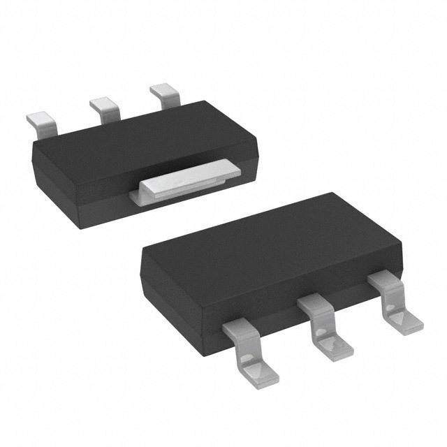
| 产品图片 |
|
| 产品型号 | Z0109MN0,135 |
| rohs | 无铅 / 符合限制有害物质指令(RoHS)规范要求 |
| 产品系列 | - |
| 三端双向可控硅类型 | 逻辑 - 灵敏栅极 |
| 供应商器件封装 | SC-73 |
| 其它名称 | 568-11068-6 |
| 包装 | Digi-Reel® |
| 安装类型 | 表面贴装 |
| 封装/外壳 | TO-261-4,TO-261AA |
| 标准包装 | 1 |
| 电压-断态 | 600V |
| 电压-栅极触发(Vgt)(最大值) | 1.3V |
| 电流-不重复浪涌50、60Hz(Itsm) | 12.5A,13.8A |
| 电流-保持(Ih)(最大值) | 10mA |
| 电流-栅极触发(Igt)(最大值) | 10mA |
| 电流-通态(It(RMS))(最大值) | 1A |
| 配置 | 单一 |
SOT223-1.jpg)


- 商务部:美国ITC正式对集成电路等产品启动337调查
- 曝三星4nm工艺存在良率问题 高通将骁龙8 Gen1或转产台积电
- 太阳诱电将投资9.5亿元在常州建新厂生产MLCC 预计2023年完工
- 英特尔发布欧洲新工厂建设计划 深化IDM 2.0 战略
- 台积电先进制程称霸业界 有大客户加持明年业绩稳了
- 达到5530亿美元!SIA预计今年全球半导体销售额将创下新高
- 英特尔拟将自动驾驶子公司Mobileye上市 估值或超500亿美元
- 三星加码芯片和SET,合并消费电子和移动部门,撤换高东真等 CEO
- 三星电子宣布重大人事变动 还合并消费电子和移动部门
- 海关总署:前11个月进口集成电路产品价值2.52万亿元 增长14.8%


PDF Datasheet 数据手册内容提取
Z0109MN0 4Q Triac 15 September 2018 Product data sheet 1. General description Planar passivated sensitive gate four quadrant triac in a SOT223 (SC-73) surface-mountable plastic package intended for applications requiring enhanced immunity to noise and direct interfacing to logic level ICs and low power gate drivers. 2. Features and benefits • Direct interfacing to logic level ICs • Enhanced current surge capability • Enhanced noise immunity • High blocking voltage capability • Planar passivated for voltage ruggedness and reliability • Sensitive gate in four quadrants • Surface-mountable package • Triggering in all four quadrants 3. Applications • General purpose low power motor control • Home appliances • Industrial process control • Low power AC Fan controllers 4. Quick reference data Table 1. Quick reference data Symbol Parameter Conditions Min Typ Max Unit V repetitive peak off- - - 600 V DRM state voltage I RMS on-state current full sine wave; T ≤ 105 °C; Fig. 1; - - 1 A T(RMS) sp Fig. 2; Fig. 3 I non-repetitive peak on- full sine wave; T = 25 °C; - - 12.5 A TSM j(init) state current t = 20 ms; Fig. 4; Fig. 5 p full sine wave; T = 25 °C; - - 13.8 A j(init) t = 16.7 ms p T junction temperature - - 125 °C j Static characteristics I gate trigger current V = 12 V; I = 0.1 A; T2+ G+; 0.4 - 10 mA GT D T T = 25 °C; Fig. 9 j
WeEn Semiconductors Z0109MN0 4Q Triac Symbol Parameter Conditions Min Typ Max Unit V = 12 V; I = 0.1 A; T2+ G-; 0.4 - 10 mA D T T = 25 °C; Fig. 9 j V = 12 V; I = 0.1 A; T2- G-; 0.4 - 10 mA D T T = 25 °C; Fig. 9 j V = 12 V; I = 0.1 A; T2- G+; 0.4 - 10 mA D T T = 25 °C; Fig. 9 j I holding current V = 12 V; T = 25 °C; Fig. 11 - - 10 mA H D j V on-state voltage I = 1.4 A; T = 25 °C; Fig. 12 - 1.3 1.6 V T T j Dynamic characteristics dV /dt rate of rise of off-state V = 402 V; T = 110 °C; (V = 67% 120 - - V/µs D DM j DM voltage of V ); exponential waveform; gate DRM open circuit; Fig. 14 dV /dt rate of change of V = 400 V; T = 110 °C; dI / 2 - - V/µs com D j com commutating voltage dt = 0.44 A/ms; gate open circuit 5. Pinning information Table 2. Pinning information Pin Symbol Description Simplified outline Graphic symbol 1 T1 main terminal 1 4 T2 T1 2 T2 main terminal 2 G sym051 3 G gate 1 2 3 4 T2 main terminal 2 SC-73 (SOT223) 6. Ordering information Table 3. Ordering information Type number Package Name Description Version Z0109MN0 SC-73 plastic surface-mounted package with increased heatsink; 4 SOT223 leads Z0109MN0 All information provided in this document is subject to legal disclaimers. © WeEn Semiconductors Co., Ltd. 2018. All rights reserved Product data sheet 15 September 2018 2 / 14
WeEn Semiconductors Z0109MN0 4Q Triac 7. Limiting values Table 4. Limiting values In accordance with the Absolute Maximum Rating System (IEC 60134). Symbol Parameter Conditions Min Max Unit V repetitive peak off-state - 600 V DRM voltage I RMS on-state current full sine wave; T ≤ 105 °C; Fig. 1; Fig. 2; - 1 A T(RMS) sp Fig. 3 I non-repetitive peak on- full sine wave; T = 25 °C; t = 20 ms; - 12.5 A TSM j(init) p state current Fig. 4; Fig. 5 full sine wave; T = 25 °C; t = 16.7 ms - 13.8 A j(init) p 2 2 I t I t for fusing t = 10 ms; SIN - 0.78 A²s p dI /dt rate of rise of on-state I = 20 mA; T2+ G+ - 50 A/µs T G current I = 20 mA; T2+ G- - 50 A/µs G IG = 20 mA; T2- G- - 50 A/µs IG = 20 mA; T2- G+ - 20 A/µs I peak gate current - 1 A GM P peak gate power - 2 W GM P average gate power over any 20 ms period - 0.1 W G(AV) T storage temperature -40 150 °C stg T junction temperature - 125 °C j 003aac269 003aac270 8 1.2 IT(RMS) IT(RMS) (A) (A) 6 0.8 4 0.4 2 0 0 10-2 10-1 1 10 -50 0 50 100 150 surgeduration(s) Tsp(°C) f = 50 Hz; T = 105 °C sp Fig. 2. RMS on-state current as a function of solder Fig. 1. RMS on-state current as a function of surge point temperature; maximum values duration; maximum values Z0109MN0 All information provided in this document is subject to legal disclaimers. © WeEn Semiconductors Co., Ltd. 2018. All rights reserved Product data sheet 15 September 2018 3 / 14
WeEn Semiconductors Z0109MN0 4Q Triac 003aac259 2.0 conduction form Ptot angle, α factor (W) (degrees) a α 1.6 30 2.816 60 1.967 α=180° 90 1.570 α 1.2 120 1.329 120° 180 1.110 90° 60° 0.8 30° 0.4 0.0 0 0.2 0.4 0.6 0.8 1 1.2 IT(RMS)(A) α = conduction angle a = form factor = I / I T(RMS) T(AV) Fig. 3. Total power dissipation as a function of RMS on-state current; maximum values 003aaf449 16 ITSM (A) 12 8 IT ITSM 4 t 1/f Tj(init)=25°Cmax 0 1 10 102 103 numberofcycles f = 50 Hz Fig. 4. Non-repetitive peak on-state current as a function of the number of sinusoidal current cycles; maximum values Z0109MN0 All information provided in this document is subject to legal disclaimers. © WeEn Semiconductors Co., Ltd. 2018. All rights reserved Product data sheet 15 September 2018 4 / 14
WeEn Semiconductors Z0109MN0 4Q Triac 003aaf490 103 IT ITSM I TSM (A) t 102 tp Tj(init)=25°Cmax (1) (2) 10 1 10-5 10-4 10-3 10-2 10-1 tp(s) t ≤ 20 ms p (1) dI /dt limit T (2) T2- G+ quadrant limit Fig. 5. Non-repetitive peak on-state current as a function of pulse width; maximum values Z0109MN0 All information provided in this document is subject to legal disclaimers. © WeEn Semiconductors Co., Ltd. 2018. All rights reserved Product data sheet 15 September 2018 5 / 14
WeEn Semiconductors Z0109MN0 4Q Triac 8. Thermal characteristics Table 5. Thermal characteristics Symbol Parameter Conditions Min Typ Max Unit R thermal resistance full cycle; Fig. 6 - - 15 K/W th(j-sp) from junction to solder point R thermal resistance in free air; printed-circuit board - 156 - K/W th(j-a) from junction to mounted: minimum footprint; full cycle; ambient free air Fig. 7 in free air; printed-circuit board - 70 - K/W mounted: pad area; full cycle; Fig. 8 102 003aac210 Zth(j-sp) (K/W) 10 1 P 10-1 tp t 10-2 10-5 10-4 10-3 10-2 10-1 1 10 tp(s) Fig. 6. Transient thermal impedance from junction to solder point as a function of pulse width Z0109MN0 All information provided in this document is subject to legal disclaimers. © WeEn Semiconductors Co., Ltd. 2018. All rights reserved Product data sheet 15 September 2018 6 / 14
WeEn Semiconductors Z0109MN0 4Q Triac 3.8min 36 1.5 min 18 6.3 60 4.6 4.5 9 1.5 2.3 min (3×) 10 1.5 min 4.6 001aab508 7 All dimensions are in mm 15 Fig. 7. Minimum footprint SOT223 50 001aab509 All dimensions are in mm Printed circuit board: FR4 epoxy glass (1.6 mm thick), copper laminate (35 um thick) Fig. 8. Printed circuit board pad area: SOT223 Z0109MN0 All information provided in this document is subject to legal disclaimers. © WeEn Semiconductors Co., Ltd. 2018. All rights reserved Product data sheet 15 September 2018 7 / 14
WeEn Semiconductors Z0109MN0 4Q Triac 9. Characteristics Table 6. Characteristics Symbol Parameter Conditions Min Typ Max Unit Static characteristics I gate trigger current V = 12 V; I = 0.1 A; T2+ G+; 0.4 - 10 mA GT D T T = 25 °C; Fig. 9 j V = 12 V; I = 0.1 A; T2+ G-; 0.4 - 10 mA D T T = 25 °C; Fig. 9 j V = 12 V; I = 0.1 A; T2- G-; 0.4 - 10 mA D T T = 25 °C; Fig. 9 j V = 12 V; I = 0.1 A; T2- G+; 0.4 - 10 mA D T T = 25 °C; Fig. 9 j I latching current V = 12 V; I = 0.1 A; T2+ G+; - - 15 mA L D G T = 25 °C; Fig. 10 j V = 12 V; I = 0.1 A; T2+ G-; - - 30 mA D G T = 25 °C; Fig. 10 j V = 12 V; I = 0.1 A; T2- G-; - - 15 mA D G T = 25 °C; Fig. 10 j V = 12 V; I = 0.1 A; T2- G+; - - 15 mA D G T = 25 °C; Fig. 10 j I holding current V = 12 V; T = 25 °C; Fig. 11 - - 10 mA H D j V on-state voltage I = 1.4 A; T = 25 °C; Fig. 12 - 1.3 1.6 V T T j V gate trigger voltage V = 12 V; I = 0.1 A; T = 25 °C; - - 1 V GT D T j Fig. 13 V = 600 V; I = 0.1 A; T = 125 °C; 0.2 - - V D T j Fig. 13 I off-state current V = 600 V; T = 125 °C - - 0.5 mA D D j Dynamic characteristics dV /dt rate of rise of off-state V = 402 V; T = 110 °C; (V = 67% 120 - - V/µs D DM j DM voltage of V ); exponential waveform; gate DRM open circuit; Fig. 14 dV /dt rate of change of V = 400 V; T = 110 °C; dI / 2 - - V/µs com D j com commutating voltage dt = 0.44 A/ms; gate open circuit Z0109MN0 All information provided in this document is subject to legal disclaimers. © WeEn Semiconductors Co., Ltd. 2018. All rights reserved Product data sheet 15 September 2018 8 / 14
WeEn Semiconductors Z0109MN0 4Q Triac 003aaa205 003aaa203 4 3 IGT IL IGT(25°C) IL(25°C) 3 (1) (2) 2 (3) (4) 2 1 1 0 0 -50 0 50 100 150 -50 0 50 100 150 Tj(°C) Tj(°C) (1) T2- G+ Fig. 10. Normalized latching current as a function of (2) T2- G- junction temperature (3) T2+ G- (4) T2+ G+ Fig. 9. Normalized gate trigger current as a function of junction temperature 003aaa204 003aac258 3 2 IT IH (A) IH(25°C) 1.6 2 1.2 0.8 (1) (2) (3) 1 0.4 0 0 -50 0 50 100 150 0 0.4 0.8 1.2 1.6 2 Tj(°C) VT (V) V = 1.13 V o Fig. 11. Normalized holding current as a function of R = 0.31 Ω s junction temperature (1) T = 125 °C; typical values j (2) T = 125 °C; maximum values j (3) T = 25 °C; maximum values j Fig. 12. On-state current as a function of on-state voltage Z0109MN0 All information provided in this document is subject to legal disclaimers. © WeEn Semiconductors Co., Ltd. 2018. All rights reserved Product data sheet 15 September 2018 9 / 14
WeEn Semiconductors Z0109MN0 4Q Triac 1.6 003aaa209 1.6 003aaa208 VGT A VGT(25°C) 1.2 1.2 0.8 0.8 0.4 0.4 0 0 -50 0 50 100 150 0 50 100 150 Tj (°C) Tj(°C) Fig. 13. Normalized gate trigger voltage as a function of junction temperature Fig. 14. Normalized critical rate of rise of off-state voltage as a function of junction temperature; typical values Z0109MN0 All information provided in this document is subject to legal disclaimers. © WeEn Semiconductors Co., Ltd. 2018. All rights reserved Product data sheet 15 September 2018 10 / 14
WeEn Semiconductors Z0109MN0 4Q Triac 10. Package outline Plasticsurface-mountedpackagewithincreasedheatsink;4leads SOT223 D B E A X c y HE v M A b1 4 Q A A1 1 2 3 Lp e1 bp w M B detailX e 0 2 4mm scale DIMENSIONS(mmaretheoriginaldimensions) UNIT A A1 bp b1 c D E e e1 HE Lp Q v w y 1.8 0.10 0.80 3.1 0.32 6.7 3.7 7.3 1.1 0.95 mm 4.6 2.3 0.2 0.1 0.1 1.5 0.01 0.60 2.9 0.22 6.3 3.3 6.7 0.7 0.85 OUTLINE REFERENCES EUROPEAN ISSUEDATE VERSION IEC JEDEC JEITA PROJECTION 04-11-10 SOT223 SC-73 06-03-16 Fig. 15. Package outline SC-73 (SOT223) Z0109MN0 All information provided in this document is subject to legal disclaimers. © WeEn Semiconductors Co., Ltd. 2018. All rights reserved Product data sheet 15 September 2018 11 / 14
WeEn Semiconductors Z0109MN0 4Q Triac Right to make changes — WeEn Semiconductors reserves the right to make changes to information published in this document, including without 11. Legal information limitation specifications and product descriptions, at any time and without notice. This document supersedes and replaces all information supplied prior to the publication hereof. Data sheet status Suitability for use — WeEn Semiconductors products are not designed, authorized or warranted to be suitable for use in life support, life-critical or safety-critical systems or equipment, nor in applications where failure Document Product Definition or malfunction of an WeEn Semiconductors product can reasonably status [1][2] status [3] be expected to result in personal injury, death or severe property or environmental damage. WeEn Semiconductors and its suppliers accept no Objective Development This document contains data from liability for inclusion and/or use of WeEn Semiconductors products in such [short] data the objective specification for product equipment or applications and therefore such inclusion and/or use is at the sheet development. customer’s own risk. Preliminary Qualification This document contains data from the Quick reference data — The Quick reference data is an extract of the [short] data preliminary specification. product data given in the Limiting values and Characteristics sections of this sheet document, and as such is not complete, exhaustive or legally binding. Product Production This document contains the product Applications — Applications that are described herein for any of these [short] data specification. products are for illustrative purposes only. WeEn Semiconductors makes sheet no representation or warranty that such applications will be suitable for the specified use without further testing or modification. [1] Please consult the most recently issued document before initiating or Customers are responsible for the design and operation of their applications completing a design. and products using WeEn Semiconductors products, and WeEn [2] The term 'short data sheet' is explained in section "Definitions". Semiconductors accepts no liability for any assistance with applications or [3] The product status of device(s) described in this document may have customer product design. It is customer’s sole responsibility to determine changed since this document was published and may differ in case of whether the WeEn Semiconductors product is suitable and fit for the multiple devices. The latest product status information is available on customer’s applications and products planned, as well as for the planned the Internet at URL http://www.ween-semi.com. application and use of customer’s third party customer(s). Customers should provide appropriate design and operating safeguards to minimize the risks associated with their applications and products. Definitions WeEn Semiconductors does not accept any liability related to any default, Draft — The document is a draft version only. The content is still under damage, costs or problem which is based on any weakness or default internal review and subject to formal approval, which may result in in the customer’s applications or products, or the application or use by modifications or additions. WeEn Semiconductors does not give any customer’s third party customer(s). Customer is responsible for doing all representations or warranties as to the accuracy or completeness of necessary testing for the customer’s applications and products using WeEn information included herein and shall have no liability for the consequences Semiconductors products in order to avoid a default of the applications of use of such information. and the products or of the application or use by customer’s third party Short data sheet — A short data sheet is an extract from a full data sheet customer(s). WeEn does not accept any liability in this respect. with the same product type number(s) and title. A short data sheet is Limiting values — Stress above one or more limiting values (as defined in intended for quick reference only and should not be relied upon to contain the Absolute Maximum Ratings System of IEC 60134) will cause permanent detailed and full information. For detailed and full information see the damage to the device. Limiting values are stress ratings only and (proper) relevant full data sheet, which is available on request via the local WeEn operation of the device at these or any other conditions above those Semiconductors sales office. In case of any inconsistency or conflict with the given in the Recommended operating conditions section (if present) or the short data sheet, the full data sheet shall prevail. Characteristics sections of this document is not warranted. Constant or Product specification — The information and data provided in a Product repeated exposure to limiting values will permanently and irreversibly affect data sheet shall define the specification of the product as agreed between the quality and reliability of the device. WeEn Semiconductors and its customer, unless WeEn Semiconductors and No offer to sell or license — Nothing in this document may be interpreted customer have explicitly agreed otherwise in writing. In no event however, or construed as an offer to sell products that is open for acceptance or the shall an agreement be valid in which the WeEn Semiconductors product grant, conveyance or implication of any license under any copyrights, patents is deemed to offer functions and qualities beyond those described in the or other industrial or intellectual property rights. Product data sheet. Export control — This document as well as the item(s) described herein may be subject to export control regulations. Export might require a prior Disclaimers authorization from competent authorities. Limited warranty and liability — Information in this document is believed Non-automotive qualified products — Unless this data sheet expressly to be accurate and reliable. However, WeEn Semiconductors does not states that this specific WeEn Semiconductors product is automotive give any representations or warranties, expressed or implied, as to the qualified, the product is not suitable for automotive use. It is neither qualified accuracy or completeness of such information and shall have no liability for nor tested in accordance with automotive testing or application requirements. the consequences of use of such information. WeEn Semiconductors takes WeEn Semiconductors accepts no liability for inclusion and/or use of non- no responsibility for the content in this document if provided by an information automotive qualified products in automotive equipment or applications. source outside of WeEn Semiconductors. In the event that customer uses the product for design-in and use in In no event shall WeEn Semiconductors be liable for any indirect, incidental, automotive applications to automotive specifications and standards, punitive, special or consequential damages (including - without limitation - customer (a) shall use the product without WeEn Semiconductors’ warranty lost profits, lost savings, business interruption, costs related to the removal of the product for such automotive applications, use and specifications, and or replacement of any products or rework charges) whether or not such (b) whenever customer uses the product for automotive applications beyond damages are based on tort (including negligence), warranty, breach of WeEn Semiconductors’ specifications such use shall be solely at customer’s contract or any other legal theory. own risk, and (c) customer fully indemnifies WeEn Semiconductors for any liability, damages or failed product claims resulting from customer Notwithstanding any damages that customer might incur for any reason design and use of the product for automotive applications beyond WeEn whatsoever, WeEn Semiconductors’ aggregate and cumulative liability Semiconductors’ standard warranty and WeEn Semiconductors’ product towards customer for the products described herein shall be limited in specifications. accordance with the Terms and conditions of commercial sale of WeEn Semiconductors. Z0109MN0 All information provided in this document is subject to legal disclaimers. © WeEn Semiconductors Co., Ltd. 2018. All rights reserved Product data sheet 15 September 2018 12 / 14
WeEn Semiconductors Z0109MN0 4Q Triac Translations — A non-English (translated) version of a document is for reference only. The English version shall prevail in case of any discrepancy between the translated and English versions. Trademarks Notice: All referenced brands, product names, service names and trademarks are the property of their respective owners. Z0109MN0 All information provided in this document is subject to legal disclaimers. © WeEn Semiconductors Co., Ltd. 2018. All rights reserved Product data sheet 15 September 2018 13 / 14
WeEn Semiconductors Z0109MN0 4Q Triac 12. Contents 1. General description......................................................1 2. Features and benefits..................................................1 3. Applications..................................................................1 4. Quick reference data....................................................1 5. Pinning information......................................................2 6. Ordering information....................................................2 7. Limiting values.............................................................3 8. Thermal characteristics...............................................6 9. Characteristics..............................................................8 10. Package outline........................................................11 11. Legal information.....................................................12 © WeEn Semiconductors Co., Ltd. 2018. All rights reserved For more information, please visit: http://www.ween-semi.com For sales office addresses, please send an email to: salesaddresses@ween-semi.com Date of release: 15 September 2018 Z0109MN0 All information provided in this document is subject to legal disclaimers. © WeEn Semiconductors Co., Ltd. 2018. All rights reserved Product data sheet 15 September 2018 14 / 14