ICGOO在线商城 > 开发板,套件,编程器 > 评估和演示板和套件 > XR21V1414IM-0B-EB
 Datasheet下载
- 型号: XR21V1414IM-0B-EB
- 制造商: Exar
- 库位|库存: xxxx|xxxx
- 要求:
| 数量阶梯 | 香港交货 | 国内含税 |
| +xxxx | $xxxx | ¥xxxx |
查看当月历史价格
查看今年历史价格
XR21V1414IM-0B-EB产品简介:
ICGOO电子元器件商城为您提供XR21V1414IM-0B-EB由Exar设计生产,在icgoo商城现货销售,并且可以通过原厂、代理商等渠道进行代购。 XR21V1414IM-0B-EB价格参考。ExarXR21V1414IM-0B-EB封装/规格:评估和演示板和套件, XR21V1414IM USB 2.0 to UART Interface Evaluation Board。您可以下载XR21V1414IM-0B-EB参考资料、Datasheet数据手册功能说明书,资料中有XR21V1414IM-0B-EB 详细功能的应用电路图电压和使用方法及教程。
MaxLinear, Inc. 的 XR21V1414IM-0B-EB 是一款评估和演示板,专为 XR21V1414 集成电路设计。XR21V1414 是一款高度集成的 USB 音频和 UART 桥接控制器,支持多通道音频和数据传输。该评估板的主要应用场景包括:

 1. USB 音频应用
   XR21V1414IM-0B-EB 适用于开发和测试基于 USB 的音频设备。它支持多达 8 个音频通道,能够处理高质量的音频流,适用于专业音频设备、声卡、会议系统等。通过 USB 接口连接到计算机或其他 USB 主机设备时,可以实现低延迟、高保真的音频传输。

 2. UART 数据通信
   该评估板还集成了 UART 接口,允许开发者测试和验证 UART 数据通信功能。这使得它适用于需要同时处理音频和数据的应用场景,例如工业控制、智能家居设备或物联网 (IoT) 网关。UART 接口可以用于调试、配置或其他数据传输任务。

 3. 嵌入式系统开发
   对于嵌入式系统开发者来说,XR21V1414IM-0B-EB 提供了一个方便的平台来评估 XR21V1414 芯片的功能。开发者可以通过该评估板快速搭建原型,进行硬件和固件的开发与调试。它支持多种操作系统(如 Windows、Linux 和 macOS),并提供了丰富的开发工具和示例代码,帮助开发者加速产品开发周期。

 4. 音频设备制造商
   音频设备制造商可以使用该评估板来测试和优化他们的产品设计。XR21V1414IM-0B-EB 支持多种音频编解码器和采样率,能够满足不同音频设备的需求。此外,它还支持 I2S 和 PCM 接口,进一步扩展了其在音频领域的应用范围。

 5. 教育和研究机构
   在教育和研究领域,XR21V1414IM-0B-EB 可以作为教学工具,帮助学生和研究人员了解 USB 音频协议、UART 通信以及嵌入式系统的开发过程。它提供了一个实际的操作平台,使学习者能够动手实践,加深对相关技术的理解。

总之,XR21V1414IM-0B-EB 评估板是一款多功能的开发工具,适用于多种应用场景,特别是在音频设备、数据通信和嵌入式系统开发中具有广泛的应用前景。
| 参数 | 数值 |
| 产品目录 | 编程器,开发系统嵌入式解决方案 |
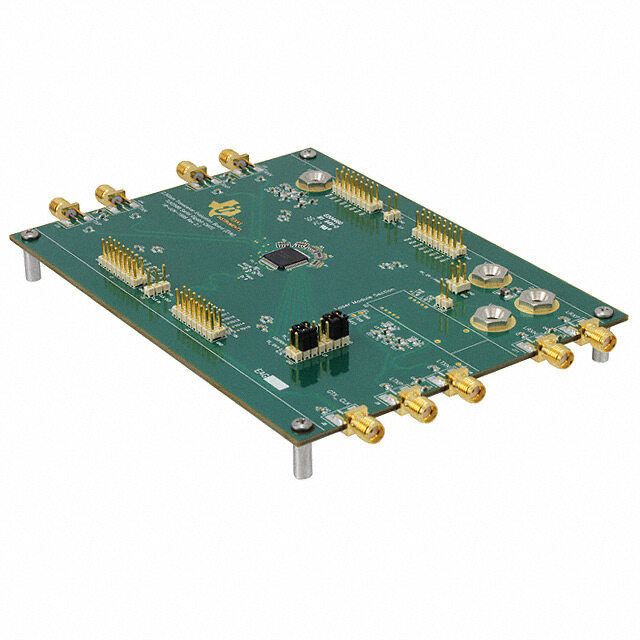
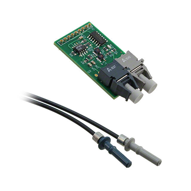
| 描述 | EVAL BOARD FOR XR21V1414界面开发工具 For XR21V1414 TQFP48 USB, RS232;No Cables |
| 产品分类 | |
| 品牌 | Exar Corporation |
| 产品手册 | http://www.exar.com/Common/Content/Document.ashx?id=20071 |
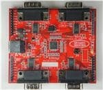
| 产品图片 |
|
| 产品系列 | 模拟与数字IC开发工具,界面开发工具,Exar XR21V1414IM-0B-EB- |
| 数据手册 | http://www.exar.com/Common/Content/Document.ashx?id=1416点击此处下载产品Datasheet |
| 产品型号 | XR21V1414IM-0B-EB |
| rohs | 无铅 / 符合限制有害物质指令(RoHS)规范要求 |
| 主要属性 | - |
| 主要用途 | 接口,USB 2.0 至 UART |
| 产品 | Evaluation Boards |
| 产品培训模块 | http://www.digikey.cn/PTM/IndividualPTM.page?site=cn&lang=zhs&ptm=25377http://www.digikey.cn/PTM/IndividualPTM.page?site=cn&lang=zhs&ptm=25557 |
| 产品种类 | 界面开发工具 |
| 使用的IC/零件 | XR21V1414IM |
| 其它名称 | 1016-1427 |
| 商标 | Exar |
| 嵌入式 | 否 |
| 工作电源电压 | 3.3 V, 5 V |
| 工具用于评估 | XR21V1414 |
| 所含物品 | 板 |
| 接口类型 | RS-232, USB |
| 标准包装 | 1 |
| 类型 | USB to UART |
| 辅助属性 | - |


- 商务部:美国ITC正式对集成电路等产品启动337调查
- 曝三星4nm工艺存在良率问题 高通将骁龙8 Gen1或转产台积电
- 太阳诱电将投资9.5亿元在常州建新厂生产MLCC 预计2023年完工
- 英特尔发布欧洲新工厂建设计划 深化IDM 2.0 战略
- 台积电先进制程称霸业界 有大客户加持明年业绩稳了
- 达到5530亿美元!SIA预计今年全球半导体销售额将创下新高
- 英特尔拟将自动驾驶子公司Mobileye上市 估值或超500亿美元
- 三星加码芯片和SET,合并消费电子和移动部门,撤换高东真等 CEO
- 三星电子宣布重大人事变动 还合并消费电子和移动部门
- 海关总署:前11个月进口集成电路产品价值2.52万亿元 增长14.8%

PDF Datasheet 数据手册内容提取
XR21V1414 4-CH FULL-SPEED USB UART DECEMBER 2013 REV. 1.3.0 GENERAL DESCRIPTION FEATURES • The XR21V1414 (V1414) is an enhanced 4-channel USB 2.0 Compliant, Full-speed (12 Mbps) USB Universal Asynchronous Receiver and ■ Supports USB suspend, resume and remote Transmitter (UART). The USB interface is fully wakeup operations compliant to Full Speed USB 2.0 specification that • ± 5 kV HBM ESD protection on USB data pins supports 12 Mbps USB data transfer rate. The USB interface also supports USB suspend, resume and • ± 2 kV HBM ESD protection on all other pins remote wakeup operations. • Enhanced Features of each UART The V1414 operates from an internal 48MHz clock ■ UART data rates up to 12 Mbps therefore no external crystal/oscillator is required like previous generation UARTs. With the fractional baud ■ Fractional Baud Rate Generator rate generator, any baud rate can accurately be ■ 128 byte TX FIFO generated using the internal 48MHz clock. ■ 384 byte RX FIFO The large 128-byte TX FIFO and 384-byte RX FIFO ■ 7, 8 or 9 data bits of the V1414 helps to optimize the overall data ■ 1 or 2 stop bits throughput for various applications. If required, the ■ Odd, even, mark, space, or no parity multidrop mode and automatic RS-485 half-duplex direction control feature further simplifies typical ■ Automatic Hardware (RTS/CTS or DTR/DSR) multidrop RS-485 applications. Flow Control ■ Automatic Software (Xon/Xoff) Flow Control The V1414 operates from a single 2.97 to 3.63 volt power supply and has 5V tolerant inputs. The V1414 ■ Multidrop mode is available in a 48-pin TQFP package. ■ Auto RS-485 Half-Duplex Control WHQL certified software drivers for Windows 2000, ■ Half-Duplex mode XP, Vista, 7, 8, and CE, as well as Linux and Mac are ■ Selectable GPIO or Modem I/O supported for the XR21V1414. • Internal 48 MHz clock APPLICATIONS • Single 3.3V power supply • Portable Appliances • 5V tolerant inputs • External Converters (dongles) • 48-pin TQFP package • Battery-Operated Devices • Virtual COM Port WHQL certified drivers • Cellular Data Devices ■ Windows 2000, XP Vista, Win7 and Win8 • Factory Automation and Process Controls ■ Windows CE 4.2, 5.0, 6.0, 7.0 • Industrial applications ■ Linux ■ Mac Exar Corporation 48720 Kato Road, Fremont CA, 94538 • (510) 668-7000 • FAX (510) 668-7017 • www.exar.com
XR21V1414 4-CH FULL-SPEED USB UART REV. 1.3.0 FIGURE 1. XR21V1414 BLOCK DIAGRAM 128-byte TX FIFO TXA Fractional 3.3V VCC 3.3V to 1.2V BRG GND Regulator 384-byte RXA RX FIFO GPIOA5/RTSA#/RS485A Internal GPIOA4/CTSA# Status and GPIOs/ GPIOA3/DTRA# Control Modem IO GPIOA2/DSRA# Registers GPIOA1/CDA# GPIOA0/RIA# USB Slave DATA+ UART Channel A Interface DATA- TXB UART Channel B RXB (Same as Ch A) GPIOB[5:0]/ModemIO SDA I2C SCL Interface UART Channel C TXC (Same as Ch A) RXC GPIOC[5:0]/ModemIO Internal 48MHz TXD UART Channel D Oscillator RXD (Same as Ch A) GPIOD[5:0]/ModemIO 2
XR21V1414 REV. 1.3.0 4-CH FULL-SPEED USB UART FIGURE 2. PIN OUT ASSIGNMENT D 5 8 4 S R # ##/ D DD R SS # T TT D D CR RI 3/ 4/5/ 0/ D DD + - D O OO C CBD BDDD DD O PI PIPI C CS SNN XX PI G GG V VU UGG RT G 48 47 46 45 44 43 42 41 40 39 38 37 GND 1 36 SCL LOWPOWER 2 35 SDA GPIOD2/DSRD# 3 34 GPIOD1/CDD# GND 4 33 VCC VCC 5 32 GND GPIOA5/RTSA#/RS485A 6 XR21V1414 31 RXA GPIOA4/CTSA# 7 48-TQFP 30 TXA TXB 8 29 GPIOC0/RIC# RXB 9 28 GPIOC1/CDC# GPIOB5/RTSB#/RS485B 10 27 GPIOC2/DSRC# GPIOB4/CTSB# 11 26 GPIOC3/DTRC# GPIOB3/DTRB# 12 25 GPIOC4/CTSC# 13 14 15 16 17 18 19 20 21 22 23 24 ## ## # CD ## CC C BB BA A CN AA XX 5 B2/DSROB1/CD OB0/RIA3/DTR A2/DSR VG OA1/CDOA0/RI TR #/RS48 PIOGPI GPIPIO PIO GPIGPI TSC G G G R 5/ C O PI G ORDERING INFORMATION PART NUMBER PACKAGE OPERATING TEMPERATURE RANGE DEVICE STATUS XR21V1414IM48-F 48-pin TQFP -40°C to +85°C Active XR21V1414IM48TR-F 48-pin TQFP -40°C to +85°C Active NOTE: TR = Tape and Reel, F = Green / RoHS 3
XR21V1414 4-CH FULL-SPEED USB UART REV. 1.3.0 PIN DESCRIPTIONS Pin Description 48-QFN NAME TYPE DESCRIPTION PIN # UART Channel A Signals RXA 31 I UART Channel A Receive Data or IR Receive Data. This pin has an inter- nal pull-up resistor. Internal pull-up resistor is not disabled during suspend mode. TXA 30 O UART Channel A Transmit Data or IR Transmit Data. GPIOA0/RIA#/ 21 I/O UART Channel A general purpose I/O or UART Ring-Indicator input RWKA# (active low) or Remote Wakeup Input (See ”Section 1.5.12, USB Sus- pend” on page 14.). This pin has an internal pull-up resistor which is disabled during suspend mode. If using this GPIO as an input, an external pull-up resistor is required to minimize the power consumption in the sus- pend mode. GPIOA1/CDA# 20 I/O UART Channel A general purpose I/O or UART Carrier-Detect input (active low). This pin has an internal pull-up resistor which is disabled dur- ing suspend mode. If using this GPIO as an input, an external pull-up resistor is required to minimize the power consumption in the suspend mode. GPIOA2/DSRA# 17 I/O UART Channel A general purpose I/O or UART Data-Set-Ready input (active low). See ”Section 1.5.6, Automatic DTR/DSR Hardware Flow Control” on page 13. This pin has an internal pull-up resistor which is disabled during suspend mode. If using this GPIO as an input, an external pull-up resistor is required to minimize the power consumption in the suspend mode. GPIOA3/DTRA# 16 I/O UART Channel A general purpose I/O or UART Data-Terminal-Ready out- put (active low). See ”Section 1.5.6, Automatic DTR/DSR Hard- ware Flow Control” on page 13. This pin has an internal pull-up resistor which is disabled during suspend mode. If using this GPIO as an input, an external pull-up resistor is required to minimize the power con- sumption in the suspend mode. GPIOA4/CTSA# 7 I/O UART Channel A general purpose I/O or UART Clear-to-Send input (active low). See ”Section 1.5.5, Automatic RTS/CTS Hardware Flow Control” on page 13. This pin has an internal pull-up resistor which is disabled during suspend mode. If using this GPIO as an input, an external pull-up resistor is required to minimize the power consumption in the suspend mode. GPIOA5/RTSA#/ 6 I/O UART Channel A general purpose I/O or UART Request-to-Send output RS485A (active low) or auto RS-485 half-duplex control. See ”Section 1.5.5, Automatic RTS/CTS Hardware Flow Control” on page 13. This pin has an internal pull-up resistor which is disabled during suspend mode. If using this GPIO as an input, an external pull-up resistor is required to minimize the power consumption in the suspend mode. UART Channel B Signals RXB 9 I UART Channel B Receive Data or IR Receive Data. This pin has an inter- nal pull-up resistor. Internal pull-up resistor is not disabled during suspend mode. 4
XR21V1414 REV. 1.3.0 4-CH FULL-SPEED USB UART Pin Description 48-QFN NAME TYPE DESCRIPTION PIN # TXB 8 O UART Channel B Transmit Data or IR Transmit Data. GPIOB0/RIB#/ 15 I/O UART Channel B general purpose I/O or UART Ring-Indicator input RWKB# (active low) or Remote Wakeup Input (See ”Section 1.5.12, USB Sus- pend” on page 14.). This pin has an internal pull-up resistor which is disabled during suspend mode. If using this GPIO as an input, an external pull-up resistor is required to minimize the power consumption in the sus- pend mode. GPIOB1/CDB# 14 I/O UART Channel B general purpose I/O or UART Carrier-Detect input (active low). This pin has an internal pull-up resistor which is disabled dur- ing suspend mode. If using this GPIO as an input, an external pull-up resistor is required to minimize the power consumption in the suspend mode. GPIOB2/DSRB# 13 I/O UART Channel B general purpose I/O or UART Data-Set-Ready input (active low). See ”Section 1.5.6, Automatic DTR/DSR Hardware Flow Control” on page 13. This pin has an internal pull-up resistor which is disabled during suspend mode. If using this GPIO as an input, an external pull-up resistor is required to minimize the power consumption in the suspend mode. GPIOB3/DTRB# 12 I/O UART Channel B general purpose I/O or UART Data-Terminal-Ready out- put (active low). See ”Section 1.5.6, Automatic DTR/DSR Hard- ware Flow Control” on page 13. This pin has an internal pull-up resistor which is disabled during suspend mode. If using this GPIO as an input, an external pull-up resistor is required to minimize the power con- sumption in the suspend mode. GPIOB4/CTSB# 11 I/O UART Channel B general purpose I/O or UART Clear-to-Send input (active low). See ”Section 1.5.5, Automatic RTS/CTS Hardware Flow Control” on page 13. This pin has an internal pull-up resistor which is disabled during suspend mode. If using this GPIO as an input, an external pull-up resistor is required to minimize the power consumption in the suspend mode. GPIOB5/RTSB#/ 10 I/O UART Channel B general purpose I/O or UART Request-to-Send output RS485B (active low) or auto RS-485 half-duplex control. See ”Section 1.5.5, Automatic RTS/CTS Hardware Flow Control” on page 13. This pin has an internal pull-up resistor which is disabled during suspend mode. If using this GPIO as an input, an external pull-up resistor is required to minimize the power consumption in the suspend mode. UART Channel C Signals RXC 23 I UART Channel C Receive Data or IR Receive Data. This pin has an inter- nal pull-up resistor. Internal pull-up resistor is not disabled during suspend mode. TXC 22 O UART Channel C Transmit Data or IR Transmit Data. GPIOC0/RIC#/ 29 I/O UART Channel C general purpose I/O or UART Ring-Indicator input RWKC# (active low) or Remote Wakeup Input (See ”Section 1.5.12, USB Sus- pend” on page 14.). This pin has an internal pull-up resistor which is disabled during suspend mode. If using this GPIO as an input, an external pull-up resistor is required to minimize the power consumption in the sus- pend mode. 5
XR21V1414 4-CH FULL-SPEED USB UART REV. 1.3.0 Pin Description 48-QFN NAME TYPE DESCRIPTION PIN # GPIOC1/CDC# 28 I/O UART Channel C general purpose I/O or UART Carrier-Detect input (active low). This pin has an internal pull-up resistor which is disabled dur- ing suspend mode. If using this GPIO as an input, an external pull-up resistor is required to minimize the power consumption in the suspend mode. GPIOC2/DSRC# 27 I/O UART Channel C general purpose I/O or UART Data-Set-Ready input (active low). See ”Section 1.5.6, Automatic DTR/DSR Hardware Flow Control” on page 13. This pin has an internal pull-up resistor which is disabled during suspend mode. If using this GPIO as an input, an external pull-up resistor is required to minimize the power consumption in the suspend mode. GPIOC3/DTRC# 26 I/O UART Channel C general purpose I/O or UART Data-Terminal-Ready out- put (active low). See ”Section 1.5.6, Automatic DTR/DSR Hard- ware Flow Control” on page 13. This pin has an internal pull-up resistor which is disabled during suspend mode. If using this GPIO as an input, an external pull-up resistor is required to minimize the power con- sumption in the suspend mode. GPIOC4/CTSC# 25 I/O UART Channel C general purpose I/O or UART Clear-to-Send input (active low). See ”Section 1.5.5, Automatic RTS/CTS Hardware Flow Control” on page 13. This pin has an internal pull-up resistor which is disabled during suspend mode. If using this GPIO as an input, an external pull-up resistor is required to minimize the power consumption in the suspend mode. GPIOC5/RTSC#/ 24 I/O UART Channel C general purpose I/O or UART Request-to-Send output RS485C (active low) or auto RS-485 half-duplex control. See ”Section 1.5.5, Automatic RTS/CTS Hardware Flow Control” on page 13. This pin has an internal pull-up resistor which is disabled during suspend mode. If using this GPIO as an input, an external pull-up resistor is required to minimize the power consumption in the suspend mode. UART Channel D Signals RXD 39 I UART Channel D Receive Data or IR Receive Data. This pin has an inter- nal pull-up resistor. Internal pull-up resistor is not disabled during suspend mode. TXD 38 O UART Channel D Transmit Data or IR Transmit Data. GPIOD0/RID#/ 37 I/O UART Channel D general purpose I/O or UART Ring-Indicator input RWKD# (active low) or Remote Wakeup Input (See ”Section 1.5.12, USB Sus- pend” on page 14.). This pin has an internal pull-up resistor which is disabled during suspend mode. If using this GPIO as an input, an external pull-up resistor is required to minimize the power consumption in the sus- pend mode. GPIOD1/CDD# 34 I/O UART Channel D general purpose I/O or UART Carrier-Detect input (active low). This pin has an internal pull-up resistor which is disabled dur- ing suspend mode. If using this GPIO as an input, an external pull-up resistor is required to minimize the power consumption in the suspend mode. 6
XR21V1414 REV. 1.3.0 4-CH FULL-SPEED USB UART Pin Description 48-QFN NAME TYPE DESCRIPTION PIN # GPIOD2/DSRD# 3 I/O UART Channel D general purpose I/O or UART Data-Set-Ready input (active low). See ”Section 1.5.6, Automatic DTR/DSR Hardware Flow Control” on page 13. This pin has an internal pull-up resistor which is disabled during suspend mode. If using this GPIO as an input, an external pull-up resistor is required to minimize the power consumption in the suspend mode. GPIOD3/DTRD# 48 I/O UART Channel D general purpose I/O or UART Data-Terminal-Ready out- put (active low). See ”Section 1.5.6, Automatic DTR/DSR Hard- ware Flow Control” on page 13. This pin has an internal pull-up resistor which is disabled during suspend mode. If using this GPIO as an input, an external pull-up resistor is required to minimize the power con- sumption in the suspend mode. GPIOD4/CTSD# 47 I/O UART Channel D general purpose I/O or UART Clear-to-Send input (active low). See ”Section 1.5.5, Automatic RTS/CTS Hardware Flow Control” on page 13. This pin has an internal pull-up resistor which is disabled during suspend mode. If using this GPIO as an input, an external pull-up resistor is required to minimize the power consumption in the suspend mode. GPIOD5/RTSD#/ 46 I/O UART Channel D general purpose I/O or UART Request-to-Send output RS485D (active low) or auto RS-485 half-duplex control. See ”Section 1.5.5, Automatic RTS/CTS Hardware Flow Control” on page 13. This pin has an internal pull-up resistor which is disabled during suspend mode. If using this GPIO as an input, an external pull-up resistor is required to minimize the power consumption in the suspend mode. USB Interface Signals USBD+ 43 I/O USB port differential data plus. This pin has a 1.5 K Ohm internal pull-up resistor. USBD- 42 I/O USB port differential data minus. I2C Interface Signals SDA 35 I/O OD I2C-controller data input/output (open-drain). An optional external I2C EEPROM can be used to store default configurations upon power-up including the USB Vendor ID and Device ID. See Table 3. A pull-up resisitor (typically 4.7 to 10k Ohms) is required. If an EEPROM is not used, this pin can be used with the SCL pin to select the Remote Wake-up and Power modes. An external pull-up or pull-down resistor is required. See Table 2. SCL 36 I/O OD I2C-controller serial input clock. An optional external I2C EEPROM can be used to store default configurations upon power-up including the USB Vendor ID and Device ID. See Table 3. A pull-up resisitor (typically 4.7 to 10k Ohms) is required. If an EEPROM is not used, this pin can be used with the SDA pin to select the Remote Wake-up and Power modes. An external pull-up or pull-down resistor is required. See Table 2. 7
XR21V1414 4-CH FULL-SPEED USB UART REV. 1.3.0 Pin Description 48-QFN NAME TYPE DESCRIPTION PIN # Miscellaneous Signals LOWPOWER 2 O Low power status output. The LOWPOWER pin will be asserted whenever it is not safe to draw the amount of current from VBUS power requested in the Device Max Power field of the Configuration Descriptor. The LOW- POWER pin will behave differently for a low power device and a high power device. • Low-power device (<= 1 unit load or 100 mA i.e. bMaxPower <= 0x32): LOWPOWER pin is asserted when the USB UART is in suspend mode. • High-power deivce (bMaxPower > 0x32): LOWPOWER pin is asserted when the USB UART is in suspend mode or when it is not yet configured. The LOWPOWER pin will be de-asserted whenever it is safe to draw the amount of current requested in the Device Maximum Power field. This pin is sampled momentarily at power-up or at any USB bus reset to configure the polarity of the LOWPOWER output during suspend mode. An external (10K) pull-up resistor will cause the LOWPOWER pin to be asserted HIGH during suspend mode. An external (3.3K) pull-down resistor will cause the LOWPOWER pin to be asserted LOW during suspend mode. Power / Ground Signals VCC 5, 18, 33, Pwr +3.3V power supply. 44, 45 GND 1, 4, 19, Pwr Power supply common, ground. 32, 40, 41 NOTE: Pin type: I=Input, O=Output, I/O= Input/output, OD=Output Open Drain. 8
XR21V1414 REV. 1.3.0 4-CH FULL-SPEED USB UART 1.0 FUNCTIONAL DESCRIPTIONS 1.1 USB interface The USB interface of the V1414 is compliant with the USB 2.0 Full-Speed Specifications. The USB configuration model presented by the V1414 to the device driver is compatible to the Abstract Control Model of the USB Communication Device Class (CDC-ACM). The V1414 uses the following set of parameters: • 1 Control Endpoint ■ Endpoint 0 as outlined in the USB specifications • 1 Configuration is supported • 2 interfaces per UART channel ■ Each UART channel has a single interrupt endpoint ■ Each UART channel have bulk-in and bulk-out endpoints 1.1.1 USB Vendor ID Exar’s USB Vendor ID is 0x04E2. This is the default Vendor ID that is used for the V1414 unless a valid EEPROM is present on the I2C interface signals. If a valid EEPROM is present, the Vendor ID from the EEPROM will be used. 1.1.2 USB Product ID The default USB Product ID for the V1414 is 0x1414. If a valid EEPROM is present, the Product ID from the EEPROM will be used. Note that Exar’s custom drivers for all Windows OS require that the Product ID be an even number for the V1414 device for proper identification of the device. 1.2 USB Device Driver The V1414 device can be used with either a standard CDC-ACM driver or a custom driver. When the CDC- ACM driver is used, the driver has no capability to read or write the V1414 device registers. Because of this, the V1414 device is initialized to the settings in Table 1. With a custom driver, all GPIOs default in hardware to inputs but these settings may be modified by the custom driver. TABLE 1: V1414 REGISTER DEFAULTSWITH CDC-ACM DRIVER REGISTER VALUE NOTES FLOW_CONTROL 0x01 Hardware flow control GPIO_MODE 0x01 RTS / CTS flow control GPIO_DIRECTION 0x08 GPIO3/DTR# configured as an output GPIO_INT_MASK 0x30 GPIO0/RI#, GPIO1/CD# and GPIO2/DSR# are interrupt sensi- tive, i.e. can cause a USB interrupt to be generated Note that when using a CDC-ACM driver, the V1414 will automatically change the bMaxPacketSize to 63 bytes to compensate for a known issue with the Microsoft CDC-ACM device driver. A register is available to change this setting with a custom driver as well. See “Section 3.4.1, CUSTOM Register Description (Read/Write)” on page 28. Although there is no ability to read / write registers when using the CDC-ACM driver, basic UART functions, including setting baud rate, character format and sending line break are supported by the CDC driver. Refer to the 4 CDC_ACM_IF USB Control Commands listed in Table 4, “Supported USB Control Commands,” on page 16. 9
XR21V1414 4-CH FULL-SPEED USB UART REV. 1.3.0 1.3 I2C Interface The I2C interface provides connectivity to an external I2C memory device (i.e. EEPROM) that can be read by the V1414 for configuration. The SDA and SCL are used to specify whether Remote Wakeup and/or Bus Powered configurations are to be supported. These pins are sampled at power-up. The following table describes how Remote Wakeup and Bus Powered support. TABLE 2: REMOTE WAKEUPAND POWER MODES REMOTE WAKE-UP SDA SCL POWER MODE SUPPORT 1 1 No Self-Powered 1 0 No Bus-Powered 0 1 Yes Self-Powered 0 0 Yes Bus-Powered 1.3.1 EEPROM Contents If SDA and SCL are both logic ’1’, the V1414 device will first confirm if there is an external EEPROM attached by attempting to read the first 8 locations of the ROM. If address 0x07 of the ROM contains the value 0x58 (as specified in Table 3), the contents of the ROM are assumed to be valid. Otherwise the EEPROM will be ignored and the SDA / SCL bits are used to indicate remote wakeup support and device power mode. The I2C address must be 0xA0. An EEPROM can be used to override default Vendor IDs and Device IDs, as well as other attributes and maximum power consumption. Exar provides an in-circuit EEPROM programming utility through the USB interface using UART Control block 0x65. Refer to Table 5, “Control Blocks,” on page 17. The EEPROM programming utility can be downloaded from the Exar website. These values are uploaded from the EEPROM to the corresponding USB Standard Device Descriptor or Standard Configuration Descriptor. For details of the USB Descriptors, refer to the USB 2.0 specifications. TABLE 3: EEPROM CONTENTS EEPROM CONTENTS ADDRESS 0 Vendor ID (LSB) 1 Vendor ID (MSB) 2 Product ID (LSB) 3 Product ID (MSB) 4 Device Attributes 5 Device Maximum Power 6 Reserved 7 Signature of 0x58 (’X’). If the signature is not correct, the contents of the EEPROM are ignored. 1.3.1.1 Vendor ID The Vendor ID value replaces the idVendor field in the USB Standard Device Descriptor. 1.3.1.2 Product ID The Product ID value replaces the idProduct field in the USB Standard Device Descriptor. 10
XR21V1414 REV. 1.3.0 4-CH FULL-SPEED USB UART 1.3.1.3 Device Attributes The Device Attributes value replaces the bmAttributes field in the USB Standard Configuration Descriptor. The default setting in the V1414 device is 0xA0. The bit field definitions are: • Bit 7 is reserved - set to ’1’ • Bit 6 is Self-powered mode - set to ’0’ for bus-powered, set to ’1’ for self-powered • Bit 5 is Remote Wakeup support - set to ’0’ for no support, set to ’1’ for remote wakeup support • Bit 4:0 are reserved - set to ’0’ 1.3.1.4 Device Maximum Power The Device Maximum Power value replaces the bMaxPower field in the USB Standard Configuration Descriptor. The value specified is in units of 2 mA. For example, the value 0x2F is decimal 47 or 94 mA. Note that the default bMaxPower of the V1414 device is 94 mA. 1.4 UART Manager The UART Manager enables/disables each UART including the TX and RX FIFOs for each UART. The UART Manager is located in a separate register block from the 4 UART channels. 1.5 UART There are 4 enhanced UART channels in the V1414. Each UART channel is independent, therefore, they will need to be initialized and configured independently. Each UART can be configured via USB control transfers from the USB host. At power-up, the V1414 will default to 9600 bps, 8 data bits, no parity bit, 1 stop bit, and no flow control. If a standard CDC driver accesses the V1414, defaults will change. See ”Section 1.2, USB Device Driver” on page 9. 1.5.1 Transmitter The transmitter consists of a 128-byte TX FIFO and a Transmit Shift Register (TSR). Once a bulk-out packet has been received and the CRC has been validated, the data bytes in that packet are written into the TX FIFO of the specified UART channel. Data from the TX FIFO is transferred to the TSR when the TSR is idle or has completed sending the previous data byte. The TSR shifts the data out onto the TX output pin at the data rate defined by the CLOCK_DIVISOR and TX_CLOCK_MASK registers. The transmitter sends the start bit followed by the data bits (starting with the LSB), inserts the proper parity-bit if enabled, and adds the stop- bit(s). The transmitter can be configured for 7 or 8 data bits with or without parity or 9 data bits without parity. If 9 bit data is selected without wide mode, the 9th bit will always be ’0’. 1.5.1.1 Wide Mode Transmit When both 9 bit data and wide mode are enabled, two bytes of data must be written. The first byte that is loaded into the TX FIFO are the first 8 bits (data bits 7-0) of the 9-bit data. Bit-0 of the second byte that is loaded into the TX FIFO is bit-8 of the 9-bit data. The data that is transmitted on the TX pin is as follows: start bit, 9-bit data, stop bit. Use the WIDE_MODE register to enable wide mode. 1.5.2 Receiver The receiver consists of a 384-byte RX FIFO and a Receive Shift Register (RSR). Data that is received in the RSR via the RX pin is transferred into the RX FIFO. Data from the RX FIFO is transferred to the USB host in response to a Bulk-In request. Depending on the mode, error / status information for that data character may or may not be stored in the RX FIFO with the data. 1.5.2.1 Normal receive operation with 7 or 8-bit data Data that is received is stored in the RX FIFO. Any parity, framing or overrun error or break status information related to the data is discarded. Receive data format is shown in Figure 3. 1.5.2.2 Normal receive operation with 9-bit data The first 8 bits of data received is stored in the RX FIFO. The 9th bit as well as any parity, framing or overrun error or break status information related to the data is discarded. 11
XR21V1414 4-CH FULL-SPEED USB UART REV. 1.3.0 FIGURE 3. NORMAL OPERATION RECEIVE DATA FORMAT 7, 8, or 9 bit data 1ST byte 7 6 5 4 3 2 1 0 7 = ‘0’ in 7 bit mode 1.5.2.3 Wide mode receive operation with 7 or 8-bit data Two bytes of data are loaded into the RX FIFO for each byte of data received. The first byte is the received data. The second byte consists of the error bits and break status. Wide mode receive data format is shown in Figure 4. 1.5.2.4 Wide mode receive operation with 9-bit data Two bytes of data are loaded into the RX FIFO for each byte of data received. The first byte is the first 8 bits of the received data. The 9th bit received is stored in the bit 0 of the second byte. The parity bit is not received / checked. The remainder of the 2nd byte consists of the framing and overrun error bits and break status. FIGURE 4. WIDE MODE RECEIVE DATA FORMAT 7 or 8 bit mode 1st byte 7 6 5 4 3 2 1 0 7 = ‘0’ in 7 bit mode 2nd byte x x x x O F B P P = Parity Error (= ‘0’ if not enabled) B = Break F = Framing Error O = Overrun Error x = ‘0’ 9 bit mode 1st byte 7 6 5 4 3 2 1 0 2nd byte x x x x O F B 8 B = Break F = Framing Error O = Overrun Error x = ‘0’ Error flags are also available from the ERROR_STATUS register and the interrupt packet, however these flags are historical flags indicating that an error has occurred since the previous request. Therefore, no conclusion can be drawn as to which specific byte(s) may have contained an actual error in this manner. 1.5.3 Rx FIFO Low Latency In normal operation all bulk-in transfers will be of maxPacketSize (64) bytes to improve throughput and to minimize host processing. When there are 64 bytes of data in the RX FIFO, the V1414 will acknowledge a bulk-in request from the host and transfer the data packet. If there is less than 64 bytes in the RX FIFO, the V1414 may NAK the bulk-in request indicating that data is not ready to transfer at that time. However, if there is less than 64 bytes in the RX FIFO and no data has been received for more than 3 character times, the V1414 will acknowledge the bulk-in request and transfer any data in the RX FIFO to the USB host. In some cases, especially when the baud rate is low, this increases latency unacceptably. The V1414 has a low latency register bit that will cause the V1414 to immediately transfer any received data in the RX FIFO to the USB host, i.e. it will not wait for 3 character times. The custom driver can automatically set the 12
XR21V1414 REV. 1.3.0 4-CH FULL-SPEED USB UART RX_FIFO_LOW_LATENCY register bit to force the V1414 to be in the low latency mode, or the user may manually set this bit. With the CDC-ACM driver, the low latency mode is automatically set whenever the baud rate is set to a value of less than 46921 bps using the CDC_ACM_IF_SET_LINE_CODING command. 1.5.4 GPIO Each UART has 6 GPIOs. By hardware default the GPIOs are configured as inputs but may be modified by a custom driver. Additionally, there are several modes that can be enabled to add additional feature such as auto RTS/CTS flow control, auto DTR/DSR flow control or auto RS-485 half duplex control. See Table 14. 1.5.5 Automatic RTS/CTS Hardware Flow Control GPIO5 and GPIO4 of the UART channel can be enabled as the RTS# and CTS# signals for Auto RTS/CTS flow control when GPIO_MODE[2:0] = ’001’ and FLOW_CONTROL[2:0] = ’001’. Automatic RTS flow control is used to prevent data overrun errors in local RX FIFO by de-asserting the RTS signal to the remote UART. When there is room in the RX FIFO, the RTS pin will be re-asserted. Automatic CTS flow control is used to prevent data overrun to the remote RX FIFO. The CTS# input is monitored to suspend/restart the local transmitter (see Figure 5): FIGURE 5. AUTO RTS AND CTS FLOW CONTROL OPERATION Local UART Remote UART UARTA UARTB Receiver FIFO RXA TXB Transmitter Trigger Reached Auto RTS RTSA# CTSB# Auto CTS Trigger Level Monitor TXA RXB Receiver FIFO Transmitter Trigger Reached Auto CTS CTSA# RTSB# Auto RTS Monitor Trigger Level 9 RTSA# 1 ON 6 OFF ON CTSB# 2 ON 7 OFF 10 ON 3 TXB 8 11 4 5 RXA 1) COM port opened, RX FIFO empty, RTSA# output is asserted 2) Signal propagated to CTSB# input 3) Data bytes enter TX FIFO, begin transmitting on TXB 4) Data propagates to Receiving device RXA 5) RX FIFO reaches threshold 6) RTSA# de-asserts 7) Signal propagates to CTSB# input 8) Transmission stops on TXB 9) USB Bulk-In empties RX FIFO below threshold, RTSA# is asserted 10) Signal propagated to CTSB# input 11) Data bytes resume transmitting on TXB 1.5.6 Automatic DTR/DSR Hardware Flow Control Auto DTR/DSR hardware flow control behaves the same as the Auto RTS/CTS hardware flow control described above except that it uses the DTR# and DSR# signals. For Auto hardware flow control, FLOW_CONTROL[2:0] = ’001’. GPIO3 and GPIO2 become DTR# and DSR#, respectively, when GPIO_MODE[2:0] = ’010’. 13
XR21V1414 4-CH FULL-SPEED USB UART REV. 1.3.0 1.5.7 Automatic XON/XOFF Software Flow Control When software flow control is enabled, the V1414 compares the receive data characters with the programmed Xon or Xoff characters. If the received character matches the programmed Xoff character, the V1414 will halt transmission as soon as the current character has completed transmission. Data transmission is resumed when a received character matches the Xon character. Software flow control is enabled when FLOW_CONTROL[2:0] = ’010’. 1.5.8 Auto RS-485 Half-Duplex Control The Auto RS-485 Half-Duplex Control feature changes the behavior of the GPIO5/RTS#/RS485 pin when enabled by the GPIO_MODE register bits 2-0. See ”Section 3.3.12, GPIO_MODE Register Description (Read/Write)” on page 26. The FLOW_CONTROL register must also be set appropriately for use in multidrop applications. See ”Section 3.3.6, FLOW_CONTROL Register Description (Read/Write)” on page 23. If enabled, the transmitter automatically asserts the GPIO5/RTS#/RS485 output prior to sending the data. By default, it de-asserts GPIO5/RTS#/RS485 following the last stop bit of the last character that has been transmitted, but the RS485_DELAY register may be used to delay the deassertion. The polarity of the GPIO5/ RTS#/RS485 signal may also be modified using the GPIO_MODE register bit 3. 1.5.9 Multidrop Mode with address matching The V1414 device has two address matching modes which are also set by the flow control register using modes 3 and 4. These modes are intended for a multi-drop network application. In these modes, the XON_CHAR register holds a unicast address and the XOFF_CHAR holds a multicast address. A unicast address is used by a transmitting master to broadcast an address to all attached slave devices that is intended for only one slave device. A multicast address is used to broadcast an address intended for more than one recipient device. Each attached slave device should have a unique unicast address value stored in the XON_CHAR register, while multiple slaves may have the same multicast adderss stored in the XOFF_CHAR register. An address match occurs when an address byte (9th bit or parity bit is ’1’) is received that matches the value stored in either the XON_CHAR or XOFF_CHAR register. 1.5.9.1 Receiver If an address match occurs in either flow control mode 3 or 4, the address byte will not be loaded into the RX FIFO, but all subsequent data bytes will be loaded into the RX FIFO. The UART Receiver will automatically be disabled when an address byte is received that does not match the values in the XON_CHAR or XOFF_CHAR register. 1.5.9.2 Transmitter In flow control mode 3, the UART transmitter is always enabled, irrespective of the Rx address match. In flow control mode 4, the UART transmitter will only be enabled if there is an Rx address match. 1.5.10 Programmable Turn-Around Delay By default, the GPIO5/RTS#/RS485 pin will be de-asserted immediately after the stop bit of the last byte has been shifted when auto RS-485 half-duplex control is enabled by the GPIO_MODE register. However, this may not be ideal for systems where the signal needs to propagate over long cables. Therefore, the de- assertion of GPIO5/RTS#/RS485 pin can be delayed from 1 to 15 bit times via the RS485_DELAY register to allow for the data to reach distant UARTs. 1.5.11 Half-Duplex Mode Half-duplex mode is enabled when FLOW_CONTROL[3] = 1. In this mode, the UART will ignore any data on the RX input when the UART is transmitting data. 1.5.12 USB Suspend All USB peripheral devices must support the USB suspend mode. Per USB standard, the V1414 device will begin to enter the Suspend state if it does not detect any activity (including Start of Frame or SOF packets) on its USB data lines for 3 ms. The device must then reduce power consumption from VBUS power within the next 7 ms to the allowed limit of 2.5 mA for the suspended state. Note that in this context, the "device" is all circuitry (including the V1414) that draws power from the host VBUS. 14
XR21V1414 REV. 1.3.0 4-CH FULL-SPEED USB UART 1.5.13 Remote Wakeup When the V1414 is suspended, the GPIO0/RI#/RWK# pin can be used to request that the host exit the Suspend state. A high to low transition on this pin will cause the device to signal a remote wakeup request to the host via a custom driver. Note that the standard CDC-ACM driver does not support this feature. In order for the remote wakeup to work, several things must be properly configured. First, the GPIO0/RI# pin must be configured as an input. Additionally, the V1414 device must have the remote wakeup feature support indicated in the USB attributes - See “Section 1.3, I2C Interface” on page 10. Lastly, the software driver must inform the USB host that the peripheral device supports the remote wake-up feature. 15
XR21V1414 4-CH FULL-SPEED USB UART REV. 1.3.0 2.0 USB CONTROL COMMANDS The following table shows all of the USB Control Commands that are supported by the V1414. Commands included are standard USB commands, CDC-ACM commands and custom Exar commands. . TABLE 4: SUPPORTED USB CONTROL COMMANDS REQUEST NAME REQUEST VALUE INDEX LENGTH DESCRIPTION TYPE DEV GET_STATUS 0x80 0 0 0 0 0 2 0 Device: remote wake-up + self-powered IF GET_STATUS 0x81 0 0 0 1-4, 0 2 0 129- Interface: zero 132 EP GET_STATUS 0x82 0 0 0 0-4, 0 2 0 129- Endpoint: halted 136 DEV CLEAR_FEATURE 0x00 1 1 0 0 0 0 0 Device remote wake-up EP CLEAR_FEATURE 0x02 1 0 0 0-4, 0 0 0 129- Endpoint halt 136 DEV SET_FEATURE 0x00 3 1 00 0 0 0 0 Device remote wake-up DEV SET_FEATURE 0x00 3 2 0 0 test 0 0 Test mode EP SET_FEATURE 0x02 3 0 0 0-4, 0 0 0 129- Endpoint halt 136 SET_ADDRESS 0x00 5 addr 0 0 0 0 0 GET_DESCRIPTOR 0x80 6 0 1 0 0 len len Device descriptor LSB MSB GET_DESCRIPTOR 0x80 6 0 2 0 0 len len Configuration descriptor LSB MSB GET_CONFIGURATION 0x80 8 0 0 0 0 1 0 SET_CONFIGURATION 0x00 9 n 0 0 0 0 0 GET_INTERFACE 0x81 10 0 0 0-7 0 1 0 CDC_ACM_IF 0x21 32 0 0 0, 2, 0 7 0 Set the UART baud rate, SET_LINE_CODING 4, 6 parity, stop bits, etc. CDC_ACM_IF 0xA1 33 0 0 0, 2, 0 7 0 Get the UART baud rate, GET_LINE_CODING 4, 6 parity, stop bits, etc. CDC_ACM_IF 0x21 34 val 0 0, 2, 0 0 0 SET_CONTROL_LINE_ 4, 6 Set UART control lines STATE 16
XR21V1414 REV. 1.3.0 4-CH FULL-SPEED USB UART TABLE 4: SUPPORTED USB CONTROL COMMANDS REQUEST NAME REQUEST VALUE INDEX LENGTH DESCRIPTION TYPE CDC_ACM_IF 0x21 35 val val 0, 2, 0 0 0 Send a break for the speci- SEND_BREAK LSB MSB 4, 6 fied duration XR_SET_REG 0x40 0 val 0 regis- block 0 0 Exar custom command: set ter one 8-bit register val: 8-bit register value register address: see Table 7 on page 19 block number: see Table 5 on page 17 XR_GETN_REG 0xC0 1 0 0 regis- block count count Exar custom register: get ter LSB MSB count 8-bit registers register address: see Table 7 on page 19 block number: see Table 5 on page 17 2.1 UART Block Numbers The table below lists the block numbers for accessing each of the UART channels and the UART Manager.. TABLE 5: CONTROL BLOCKS BLOCK NAME BLOCK NUMBER DESCRIPTION UART Channel A 0 The configuration and control registers for UART channel A. UART Channel B 1 The configuration and control registers for UART channel B. UART Channel C 2 The configuration and control registers for UART channel C. UART Channel D 3 The configuration and control registers for UART channel D. UART Manager 4 The control registers for the UART Manager. The UART Manager enables/disables the TX and RX FIFOs for each UART. I2C EEPROM 0x65 Accesses external EEPROM via I2C interface. UART Custom 0x66 Custom UART control registers. Enables / disables for wide mode, low latency mode and custom interrupt packet. 17
XR21V1414 4-CH FULL-SPEED USB UART REV. 1.3.0 3.0 REGISTER SET DESCRIPTION The internal register set of the V1414 consists of 3 different blocks of registers: the UART Manager, UART registers and UART miscellaneous registers. The UART Manager controls the TX and RX enables and FIFOs of all UART channels. The UART registers configure and control the remaining UART channel functionality with the exception of low latency mode, wide mode and custom interrupt packet enables in the UART custom register block. Registers are accessed only via the USB interface by the XR_SET_REG and XR_GET_REG commands listed in Table 4. The register address offsets are given in Table 6, Table 7 and Table 15, and the register blocks are given in Table 5. 3.1 UART Manager Registers.. TABLE 6: UART MANAGER REGISTERS ADDRESS REGISTER NAME BIT-7 BIT-6 BIT-5 BIT-4 BIT-3 BIT-2 BIT-1 BIT-0 0X10 FIFO_ENABLE_CHA 0 0 0 0 0 0 RX TX 0X11 FIFO_ENABLE_CHB 0 0 0 0 0 0 RX TX 0X12 FIFO_ENABLE_CHC 0 0 0 0 0 0 RX TX 0x13 FIFO_ENABLE_CHD 0 0 0 0 0 0 RX TX 0X18 RX_FIFO_RESET_CHA Bit-7 Bit-6 Bit-5 Bit-4 Bit-3 Bit-2 Bit-1 Bit-0 0X19 RX_FIFO_RESET_CHB Bit-7 Bit-6 Bit-5 Bit-4 Bit-3 Bit-2 Bit-1 Bit-0 0x1A RX_FIFO_RESET_CHC Bit-7 Bit-6 Bit-5 Bit-4 Bit-3 Bit-2 Bit-1 Bit-0 0x1B RX_FIFO_RESET_CHD Bit-7 Bit-6 Bit-5 Bit-4 Bit-3 Bit-2 Bit-1 Bit-0 0x1C TX_FIFO_RESET_CHA Bit-7 Bit-6 Bit-5 Bit-4 Bit-3 Bit-2 Bit-1 Bit-0 0x1D TX_FIFO_RESET_CHB Bit-7 Bit-6 Bit-5 Bit-4 Bit-3 Bit-2 Bit-1 Bit-0 0x1E TX_FIFO_RESET_CHC Bit-7 Bit-6 Bit-5 Bit-4 Bit-3 Bit-2 Bit-1 Bit-0 0x1F TX_FIFO_RESET_CHD Bit-7 Bit-6 Bit-5 Bit-4 Bit-3 Bit-2 Bit-1 Bit-0 3.1.1 FIFO_ENABLE Registers Enables the RX FIFO and TX FIFOs. For proper functionality, the UART TX and RX must be enabled in the following order: FIFO_ENABLE_CHx = 0x1 // Enable TX FIFO UART_ENABLE = 0x3 // Enable TX and RX of that channel FIFO_ENABLE_CHx = 0x3 // Enable RX FIFO 3.1.2 RX_FIFO_RESET and TX_FIFO_RESET Registers Writing a non-zero value to these registers resets the FIFOs. 18
XR21V1414 REV. 1.3.0 4-CH FULL-SPEED USB UART 3.2 UART Register Map TABLE 7: UART REGISTERS ADDRESS REGISTER NAME BIT-7 BIT-6 BIT-5 BIT-4 BIT-3 BIT-2 BIT-1 BIT-0 0X00 Reserved 0 0 0 0 0 0 0 0 0X01 Reserved 0 0 0 0 0 0 0 0 0X02 Reserved 0 0 0 0 0 0 0 0 0X03 UART_ENABLE 0 0 0 0 0 0 RX TX 0X04 CLOCK_DIVISOR0 Bit-7 Bit-6 Bit-5 Bit-4 Bit-3 Bit-2 Bit-1 Bit-0 0x05 CLOCK_DIVISOR1 Bit-15 Bit-14 Bit-13 Bit-12 Bit-11 Bit-10 Bit-9 Bit-8 0x06 CLOCK_DIVISOR2 0 0 0 0 0 Bit-18 Bit-17 Bit-16 0x07 TX_CLOCK_MASK0 Bit-7 Bit-6 Bit-5 Bit-4 Bit-3 Bit-2 Bit-1 Bit-0 0x08 TX_CLOCK_MASK1 Bit-15 Bit-14 Bit-13 Bit-12 Bit-11 Bit-10 Bit-9 Bit-8 0x09 RX_CLOCK_MASK0 Bit-7 Bit-6 Bit-5 Bit-4 Bit-3 Bit-2 Bit-1 Bit-0 0x0A RX_CLOCK_MASK1 Bit-15 Bit-14 Bit-13 Bit-12 Bit-11 Bit-10 Bit-9 Bit-8 0x0B CHARACTER_FORMAT Stop Parity Data Bits 0x0C FLOW_CONTROL Half- 0 0 0 0 Flow Control Mode Select Duplex 0x0D Reserved 0 0 0 0 0 0 0 0 0x0E Reserved 0 0 0 0 0 0 0 0 0x0F Reserved 0 0 0 0 0 0 0 0 0x10 XON_CHAR Bit-7 Bit-6 Bit-5 Bit-4 Bit-3 Bit-2 Bit-1 Bit-0 0x11 XOFF_CHAR Bit-7 Bit-6 Bit-5 Bit-4 Bit-3 Bit-2 Bit-1 Bit-0 0x12 LOOPBACK_CTL 0 0 0 0 0 En Chan 0x13 ERROR_STATUS Break Overrun Parity Framing Break 0 0 0 Status Error Error Error Error 0x14 TX_BREAK Bit-7 Bit-6 Bit-5 Bit-4 Bit-3 Bit-2 Bit-1 Bit-0 0x15 RS485_DELAY 0 0 0 0 Delay 0x16 Reserved 0 0 0 0 0 0 0 0 0x17 Reserved 0 0 0 0 0 0 0 0 0x18 Reserved 0 0 0 0 0 0 0 0 0x19 Reserved 0 0 0 0 0 0 0 0 0x1A GPIO_MODE RS485 0 0 0 0 Mode Select Polarity 0x1B GPIO_DIRECTION 0 0 GPIO5 GPIO4 GPIO3 GPIO2 GPIO1 GPIO0 0x1C GPIO_INT_MASK 0 0 GPIO5 GPIO4 GPIO3 GPIO2 GPIO1 GPIO0 0x1D GPIO_SET 0 0 GPIO5 GPIO4 GPIO3 GPIO2 GPIO1 GPIO0 0x1E GPIO_CLEAR 0 0 GPIO5 GPIO4 GPIO3 GPIO2 GPIO1 GPIO0 0x1F GPIO_STATUS 0 0 GPIO5 GPIO4 GPIO3 GPIO2 GPIO1 GPIO0 19
XR21V1414 4-CH FULL-SPEED USB UART REV. 1.3.0 3.3 UART Register Descriptions All register bits default to a value of ’0’ unless otherwise noted. 3.3.1 UART_ENABLE Register Description (Read/Write) This register enables the UART TX and RX. For proper functionality, the UART TX and RX must be enabled in the following order: FIFO_ENABLE_CHx = 0x1 // Enable TX FIFO UART_ENABLE = 0x3 // Enable TX and RX of that channel FIFO_ENABLE_CHx = 0x3 // Enable RX FIFO UART_ENABLE[0]: Enable UART TX • Logic 0 = UART TX disabled. • Logic 1 = UART TX enabled. UART_ENABLE[1]: Enable UART RX • Logic 0 = UART RX disabled. • Logic 1 = UART RX enabled. UART_ENABLE[7:2]: Reserved These bits are reserved and should remain ’0’. 3.3.2 CLOCK_DIVISOR0, CLOCK_DIVISOR1, CLOCK_DIVISOR2 Register Description (Read/Write) These registers are used for programming the baud rate. The V1414 uses a 19-bit divisor and 16-bit mask register. Using the internal 48MHz oscillator, the 19-bit divisor is calculated as follows: CLOCK_DIVISOR = Trunc ( 48000000 / Baud Rate ) For example, if the the baud rate is 115200bps, then CLOCK_DIVISOR = Trunc ( 48000000 / 115200 ) = Trunc (416.66667) = 416 CLOCK_DIVISOR0[7:0]: Baud rate clock divisor bits [7:0] CLOCK_DIVISOR1[7:0]: Baud rate clock divisor bits [15:8] CLOCK_DIVISOR2[2:0]: Baud rate clock divisor bits [18:16] CLOCK_DIVISOR2[7:3]: Reserved These bits are reserved and should remain ’0’. 3.3.3 TX_CLOCK_MASK0, TX_CLOCK_MASK1 Register Description (Read/Write) A look-up table is used for the value of the 16-bit TX Clock mask registers. The index of the look-up table is calculated as follows: index = Trunc ( ( ( 48000000 / Baud Rate ) - CLOCK_DIVISOR ) * 32) For example, if the baud rate is 115200bps, then the index will be: index = Trunc ( ( ( 48000000 / 115200 ) - 416 ) * 32) = Trunc (21.3333) = 21 The values for some baud rates to program the TX_CLOCK_MASK registers are listed in Table 8. For baud rates that are not listed, use the index to select TX_CLOCK_MASK register values from Table 9. 3.3.4 RX_CLOCK_MASK0, RX_CLOCK_MASK1 Register Description (Read/Write) The values for some baud rates to program the RX_CLOCK_MASK registers are listed in Table 8. For baud rates that are not listed, use the same index calculated for the TX_CLOCK_MASK register to select RX_CLOCK_MASK register values from Table 9. 20
XR21V1414 REV. 1.3.0 4-CH FULL-SPEED USB UART TABLE 8: CLOCK DIVISORAND CLOCK MASK VALUESFOR COMMON BAUD RATES BAUD RATE (BPS) CLOCK DIVISOR (DECIMAL) TX CLOCK MASK (HEX) RX CLOCK MASK (HEX) 1200 40000 0x0000 0x0000 2400 20000 0x0000 0x0000 4800 10000 0x0000 0x0000 9600 5000 0x0000 0x0000 19200 2500 0x0000 0x0000 38400 1250 0x0000 0x0000 57600 833 0x0912 0x0924 115200 416 0x0B6D 0x0B6A 230400 208 0x0912 0x0924 460800 104 0x0208 0x0040 500000 96 0x0000 0x0000 576000 83 0x0912 0x0924 921600 52 0x0040 0x0000 1000000 48 0x0000 0x0000 1152000 41 0x0B6D 0x0DB6 1500000 32 0x0000 0x0000 2000000 24 0x0000 0x0000 2500000 19 0x0104 0x0108 3000000 16 0x0000 0x0000 3125000 15 0x0492 0x0492 3500000 13 0x076D 0x0BB6 4000000 12 0x0000 0x0000 4250000 11 0x0122 0x0224 6250000 7 0x0B6D 0x0DB6 8000000 6 0x0000 0x0000 12000000 4 0x0000 0x0000 For baud rates that are not listed in the table above, use the index value calcuated using the formula in “Section 3.3.3, TX_CLOCK_MASK0, TX_CLOCK_MASK1 Register Description (Read/Write)” on page 20 to determine which TX Clock and RX Clock Mask register values to use from Table 9. For the the RX Clock Mask register, there are 2 values listed and would depend on whether the Clock Divisor is even or odd. For even Clock Divisors, use the value from the first column. For odd Clock Divisors, use the value from the last column. 21
XR21V1414 4-CH FULL-SPEED USB UART REV. 1.3.0 TABLE 9: TX AND RX CLOCK MASK VALUES INDEX RX CLOCK MASK (HEX) - RX CLOCK MASK (HEX) - TX CLOCK MASK (HEX) (DECIMAL) EVEN CLOCK DIVISOR ODD CLOCK DIVISOR 0 0x0000 0x0000 0x0000 1 0x0000 0x0000 0x0000 2 0x0100 0x0000 0x0100 3 0x0020 0x0400 0x0020 4 0x0010 0x0100 0x0010 5 0x0208 0x0040 0x0208 6 0x0104 0x0820 0x0108 7 0x0844 0x0210 0x0884 8 0x0444 0x0110 0x0444 9 0x0122 0x0888 0x0224 10 0x0912 0x0448 0x0924 11 0x0492 0x0248 0x0492 12 0x0252 0x0928 0x0292 13 0x094A 0x04A4 0x0A52 14 0x052A 0x0AA4 0x054A 15 0x0AAA 0x0954 0x04AA 16 0x0AAA 0x0554 0x0AAA 17 0x0555 0x0AD4 0x05AA 18 0x0B55 0x0AB4 0x055A 19 0x06B5 0x05AC 0x0B56 20 0x05B5 0x0D6C 0x06D6 21 0x0B6D 0x0B6A 0x0DB6 22 0x076D 0x06DA 0x0BB6 23 0x0EDD 0x0DDA 0x076E 24 0x0DDD 0x0BBA 0x0EEE 25 0x07BB 0x0F7A 0x0DDE 26 0x0F7B 0x0EF6 0x07DE 27 0x0DF7 0x0BF6 0x0F7E 28 0x07F7 0x0FEE 0x0EFE 29 0x0FDF 0x0FBE 0x07FE 30 0x0F7F 0x0EFE 0x0FFE 31 0x0FFF 0x0FFE 0x0FFD 22
XR21V1414 REV. 1.3.0 4-CH FULL-SPEED USB UART 3.3.5 CHARACTER_FORMAT Register Description (Read/Write) This register controls the character format such as the word length (7, 8 or 9), parity (odd, even, forced ’0’, or forced ’1’) and number of stop bits (1 or 2). CHARACTER_FORMAT[3:0]: Data Bits. TABLE 10: DATA BITS DATA BITS CHARACTER_FORMAT[3:0] 7 0111 8 1000 9 1001 All other values for CHARACTER_FORMAT[3:0] are reserved. CHARACTER_FORMAT[6:4]: Parity Mode Select These bits select the parity mode. If 9-bit data mode has been selected, then writing to these bits will not have any effect. In other words, there will not be an additional parity bit. TABLE 11: PARITY SELECTION BIT-6 BIT-5 BIT-4 PARITYSELECTION 0 0 0 No parity 0 0 1 Odd parity 0 1 0 Even parity 0 1 1 Force parity to mark, “1” 1 0 0 Force parity to space, “0” CHARACTER_FORMAT[7]: Stop Bit select This register selects the number of stop bits to add to the transmitted character and how many stop bits to check for in the received character. TABLE 12: STOP BIT SELECTION BIT-7 NUMBEROF STOP BITS 0 1 stop bit 2 2 stop bits 3.3.6 FLOW_CONTROL Register Description (Read/Write) These registers select the flow control mode. These registers should only be written to when the UART is disabled. Writing to the FLOW_CONTROL register when the UART is enabled will result in undefined behavior. Note that the FLOW_CONTROL register settings are used in conjunction with the GPIO_MODE register. 23
XR21V1414 4-CH FULL-SPEED USB UART REV. 1.3.0 FLOW_CONTROL[2:0]: Flow control mode select TABLE 13: FLOW CONTROL MODE SELECTION MODE BIT-2 BIT-1 BIT-0 MODE DESCRIPTION 0 0 0 0 No flow control, no address matching. 1 0 0 1 HW flow control enabled. Auto RTS/CTS or DTR/DSR must be selected by GPIO_MODE. 2 0 1 0 SW flow control enabled 3 0 1 1 Multidrop mode - RX only after address match, TX independent. (Typically used with GPIO_MODE 3) 4 1 0 0 Multidrop mode - RX / TX only after address match. (Typically used with GPIO_MODE 4) FLOW_CONTROL[3]: Half-Duplex Mode • Logic 0 = Normal (full-duplex) mode. The UART can transmit and receive data at the same time. • Logic 1 = Half-duplex Mode. In half-duplex mode, any data on the RX pin is ignored when the UART is transmitting data. FLOW_CONTROL[7:4]: Reserved These bits are reserved and should remain ’0’. 3.3.7 XON_CHAR, XOFF_CHAR Register Descriptions (Read/Write) The XON_CHAR and XOFF_CHAR registers store the XON and XOFF characters, respectively, that are used in the Automatic Software Flow control. XON_CHAR[7:0]: XON Character In Automatic Software Flow control mode, the UART will resume data transmission when the XON character has been received. For behavior in the Address Match mode, see “Section 1.5.9, Multidrop Mode with address matching” on page 14. For behavior in the Address Match with TX Flow Control mode, see “Section 1.5.9, Multidrop Mode with address matching” on page 14. XOFF_CHAR[7:0]: XOFF Character In Automatic Software Flow control mode, the UART will suspend data transmission when the XOFF character has been received. For behavior in the Address Match mode, see “Section 1.5.9, Multidrop Mode with address matching” on page 14. For behavior in the Address Match with TX Flow Control mode, see “Section 1.5.10, Programmable Turn- Around Delay” on page 14. 24
XR21V1414 REV. 1.3.0 4-CH FULL-SPEED USB UART 3.3.8 LOOPBACK_CTL Register Descriptions (Read/Write) LOOPBACK_CTL[1:0]: Channel • Value 0 = UART Channel A • Value 1 = UART Channel B • Value 2 = UART Channel C • Value 3 = UART Channel D LOOPBACK_CTL[2]: Enable • Logic 0 = Internal UART (TX to RX) loopback is disabled. • Logic 1 = Internal UART (TX to RX) loopback is enabled. LOOPBACK_CTL[7:3]: Reserved These bits are reserved and should remain ’0’. 3.3.9 ERROR_STATUS Register Description - Read-only This register reports any errors that may have occurred on the line such as framing, parity and overrun as well as break status. ERROR_STATUS[2:0]: Reserved These bits are reserved. Any values read from these bits should be ignored. ERROR_STATUS[3]: Break status • Logic 0 = No break condition • Logic 1 = A break condition has been detected (clears after read). ERROR_STATUS[4]: Framing Error • Logic 0 = No framing error • Logic 1 = A framing error has been detected (clears after read). A framing error occurs when a stop bit is not present when it is expected. ERROR_STATUS[5]: Parity Error • Logic 0 = No parity error • Logic 1 = A parity error has been detected (clears after read). ERROR_STATUS[6]: Overrun Error • Logic 0 = No overrun error • Logic 1 = An overrun error has been detected (clears after read). An overrun error occurs when the RX FIFO is full and another byte of data is received. ERROR_STATUS[7]: Break Status • Logic 0 = Break condition is no longer present. • Logic 1 = Break condition is currently being detected. 3.3.10 TX_BREAK Register Description (Read/Write) Writing a non-zero value to this register causes a break condition to be generated continuously until the register is cleared. If data is being shifted out of the TX pin, the data will be completely shifted out before the break condition is generated. 25
XR21V1414 4-CH FULL-SPEED USB UART REV. 1.3.0 3.3.11 RS485_DELAY Register Description (Read/Write) RS485_DELAY[3:0]: Turn-around delay This is the number of bit times the V1414 waits before de-asserting the GPIO5/RTS#/RS485 pin when it is configured for automatic RS-485 half-duplex control. RS485_DELAY[7:4]: Reserved These bits are reserved and should be ’0’. 3.3.12 GPIO_MODE Register Description (Read/Write) GPIO_MODE[2:0]: GPIO Mode Select There are 4 modes of operation for the GPIOs. The descriptions can be found in “Section 1.5, UART” on page 11. TABLE 14: GPIO MODES BITS GPIO0 GPIO1 GPIO2 GPIO3 GPIO4 GPIO5 MODE DESCRIPTION [2:0] 000 GPIO0 GPIO1 GPIO2 GPIO3 GPIO4 GPIO5 GPIO Mode, All GPIO pins available as GPIO 001 GPIO0 GPIO1 GPIO2 GPIO3 CTS# RTS# GPIO4 and GPIO5 used for Auto RTS/CTS HW Flow Control 010 GPIO0 GPIO1 DSR# DTR# GPIO4 GPIO5 GPIO2 and GPIO3 used for Auto DTR/DSR HW Flow Control 011 GPIO0 GPIO1 GPIO2 GPIO3 GPIO4 RS485 GPIO5 used for auto RS-485 half-duplex control 100 GPIO0 GPIO1 GPIO2 GPIO3 GPIO4 RS485 GPIO5 used for auto RS-485 half-duplex control after address match (See FLOW_CONTROL mode 4). GPIO_MODE[3]: RS485 Polarity • Logic 0 = GPIO5/RTS#/RS485 Low for TX • Logic 1 = GPIO5/RTS#/RS485 High for TX GPIO_MODE[7:4]: Reserved These register bits are reserved. When writing to these bits, the value should be ’0’. When reading from these bits, they are undefined and should be ignored. 3.3.13 GPIO_DIRECTION Register Description (Read/Write) This register controls the direction of pins configured as GPIO. (Pins configured for UART functions via the GPIO_MODE register, e.g. RTS# are not controlled or reported in the GPIO_DIRECTION register.) GPIO_DIRECTION[5:0]: GPIOx Direction • Logic 0 = GPIOx is an input. • Logic 1 = GPIOx is an output. GPIO_DIRECTION[7:6]: Reserved These register bits are reserved and should be ’0’. 3.3.14 GPIO_INT_MASK Register Description (Read/Write) Enables / disables generation of a USB interrupt packet at the change of state of GPIO pins when they are configured as inputs. 26
XR21V1414 REV. 1.3.0 4-CH FULL-SPEED USB UART GPIO_INT_MASK[5:0]: GPIOx Interrupt Mask • Logic 0 = A change on this input causes the device to generate an interrupt packet. • Logic 1 = A change on this input does not cause the device to generate an interrupt packet. GPIO_INT_MASK[7:6]: Reserved These register bits are reserved and should be ’0’. 3.3.15 GPIO_SET Register Description (Read/Write) Writing a ’1’ in this register drives the GPIO output high. Writing a ’0’ to a bit has no effect. Bits 7-6 are unused and should be ’0’. 3.3.16 GPIO_CLEAR Register Description (Read/Write) Writing a ’1’ in this register drives the GPIO output low. Writing a ’0’ to a bit has no effect. Bits 7-6 are unused and should be ’0’. 3.3.17 GPIO_STATUS Register Description (Read-Only) This register reports the current state of the GPIO pin. 3.4 UART Custom Registers TABLE 15: UART CUSTOM REGISTERS ADDRESS REGISTER NAME BIT-7 BIT-6 BIT-5 BIT-4 BIT-3 BIT-2 BIT-1 BIT-0 0X03 UART CHAN A CUSTOM MaxPkt- WIDE_E 0 0 0 0 0 0 Size N 0X04 UART CHAN A 0 0 0 0 0 0 0 EN LOW_LATENCY 0X06 UART CHAN A 0 GPIO5 GPIO4 GPIO3 GPIO0 0 GPIO2 GPIO1 CUSTOM_INT_PACKET 0X0B UART CHAN B CUSTOM 0 0 0 0 0 0 MaxPktSize WIDE_EN 0X0C UART CHAN B 0 0 0 0 0 0 0 EN LOW_LATENCY 0X0E UART CHAN B 0 GPIO5 GPIO4 GPIO3 GPIO0 0 GPIO2 GPIO1 CUSTOM_INT_PACKET 0X13 UART CHAN C CUSTOM 0 0 0 0 0 0 MaxPktSize WIDE_EN 0X14 UART CHAN C 0 0 0 0 0 0 0 EN LOW_LATENCY 0X16 UART CHAN C 0 GPIO5 GPIO4 GPIO3 GPIO0 0 GPIO2 GPIO1 CUSTOM_INT_PACKET 0X1B UART CHAN D CUSTOM 0 0 0 0 0 0 MaxPktSize WIDE_EN 0X1C UART CHAN D 0 0 0 0 0 0 0 EN LOW_LATENCY 0X1E UART CHAN D 0 GPIO5 GPIO4 GPIO3 GPIO0 0 GPIO2 GPIO1 CUSTOM_INT_PACKET 27
XR21V1414 4-CH FULL-SPEED USB UART REV. 1.3.0 3.4.1 CUSTOM Register Description (Read/Write) This register enables the Wide mode functionality for the UART. CUSTOM[0]: Enable wide mode • Logic 0 = Normal (7, 8 or 9 bit data) mode • Logic 1 = Wide mode - See “Section 1.5.1.1, Wide Mode Transmit” on page 11, “Section 1.5.2.3, Wide mode receive operation with 7 or 8-bit data” on page 12 and “Section 1.5.2.4, Wide mode receive operation with 9-bit data” on page 12. CUSTOM[1]: Max Packet Size • Logic 0 = bMaxPacketSize = 64 bytes Logic 1 = bMaxPacketSize = 63 bytes (this bit is automatically set to ’1’ if the XR21V1414 receives a CDC_ACM USB command) CUSTOM[7:2]: Reserved These bits are reserved and should remain ’0’. 3.4.2 LOW_LATENCY Register Description (Read/Write) This register is automatically set to logic ’1’ for baud rates below 46921 bps, and can be manually set for baud rates of 46921 bps and higher. This register enables the Low latency feature of the UART. Write to this register following any desired baud rate setting change. LOW_LATENCY[0]: Enable Low Latency mode • Logic 0 = Receive data is not forwarded from the Rx FIFO until bMaxPacketSize (64 bytes) or timeout (3 characters) has occurred. • Logic 1 = All data in the RX FIFO is provided to the USB host at the next BULK IN request irrespective of the number of bytes in the FIFO. LOW_LATENCY[7:1]: Reserved These bits are reserved and should remain ’0’. 3.4.3 CUSTOM_INT_PACKET (Read/Write) This register is used to enable / disable GPIO status in the high data byte of the custom interrupt packet. See Table 16, “Interrupt Packet Format,” on page 29 and Table 18, “Data Field of Customized Interrupt Packet - Exar Vendor Specific,” on page 30. CUSTOM_INT_PACKET[0]: GPIO1 • Logic 0 = Disable GPIO1 status in custom interrupt packet. • Logic 1 = Enable GPIO1 status in custom interrupt packet. 28
XR21V1414 REV. 1.3.0 4-CH FULL-SPEED USB UART CUSTOM_INT_PACKET[1]: GPIO2 • Logic 0 = Disable GPIO2 status in custom interrupt packet. • Logic 1 = Enable GPIO2 status in custom interrupt packet. CUSTOM_INT_PACKET[2]: Reserved • This bit is reserved and should remain ’0’. CUSTOM_INT_PACKET[3]: GPIO0 • Logic 0 = Disable GPIO0 status in custom interrupt packet. • Logic 1 = Enable GPIO0 status in custom interrupt packet. CUSTOM_INT_PACKET[4]: GPIO3 • Logic 0 = Disable GPIO3 status in custom interrupt packet. • Logic 1 = Enable GPIO3 status in custom interrupt packet. CUSTOM_INT_PACKET[5]: GPIO4 • Logic 0 = Disable GPIO4 status in custom interrupt packet. • Logic 1 = Enable GPIO4 status in custom interrupt packet. CUSTOM_INT_PACKET[6]: GPIO5 • Logic 0 = Disable GPIO5 status in custom interrupt packet. • Logic 1 = Enable GPIO5 status in custom interrupt packet. CUSTOM_INT_PACKET[7]: Reserved This bit is reserved and should remain ’0’. TABLE 16: INTERRUPT PACKET FORMAT SIZE OFFSET FIELD VALUE DESCRIPTION (BYTES) 0 bmRequestType 1 8’b10100001 D7 = Device-to-host direction D6:5 = Class Type D4-0: = Interface Recipient 1 bNotification 1 8’h20 Defined encoding for SERIAL_STATE 2 wValue 2 16’h0000 4 wIndex 2 16’h0000 D15-8 = Reserved (0) D7-0 = Interface number, 8’h00 for the CDC Com- mand Interface 6 wLength 2 16’h0002 2 bytes of transferred data 8 Data 2 Standard D15-7 = Reserved (0) int_status D6 = bOverRun (See Table 17 D5 = bParity or Table 18) D4 = bFraming D3 = bRingSignal (RI) D2 = bBreak D1 = bTxCarrier (DSR) D0 = bRxCarrier (CD) 29
XR21V1414 4-CH FULL-SPEED USB UART REV. 1.3.0 TABLE 17: DATA FIELDOF STANDARD INTERRUPT PACKET BIT(S) FIELD DESCRIPTION D15..D7 Reserved (0) D6 bOverRun Received data has been discarded due to overrun in the device. D5 bParity A parity error has occured. D4 bFraming A framing error has occured. D3 bRingSignal State of ring signal detection of the device. D2 bBreak State of break detection mechanism of the device. D1 bTxCarrier State of transmission carrier. This signal corresponds to V.24 signal 106 and RS-232 signal DSR. D0 bRxCarrier State of receiver carrier detection mechanism of device. This signal corre- sponds to V.24 signal 109 and RS-232 signal DCD. If the Exar vendor specific packet mapping is enabled then the data field also includes status for all of the UART / GPIO pins as follows: TABLE 18: DATA FIELDOF CUSTOMIZED INTERRUPT PACKET - EXAR VENDOR SPECIFIC BIT(S) FIELD DESCRIPTION 15 D15 Reserved (0) 14 D14 bGPIO5 (RTS) 13 D13 bGPIO4 (CTS) 12 D12 bGPIO3 (DTR) 11 D11 bGPIO0 (RI) 10 D10 Reserved (0) 9 D9 bGPIO2 (DSR) 8 D8 bGPIO1 (CD) 7 D7 Reserved (0) 6 D6 bOverRun 5 D5 bParity 4 D4 bFraming 3 D3 bRingSignal (RI) 2 D2 bBreak 1 D1 bTxCarrier (DSR) 0 D0 bRxCarrier (CD) 30
XR21V1414 REV. 1.3.0 4-CH FULL-SPEED USB UART 4.0 ELECTRICAL CHARACTERISTICS TABLE 19: ABSOLUTE MAXIMUM RATINGS PARAMETER RATING UNIT Vcc Supply Voltage + 4.0 V Input Voltage (all pins except USBD+ and USBD-) - 0.3 to + 6.0 V Input Voltage (USBD+ and USBD-) - 0.3 to + 5.75 V Junction Temperature 125 deg. C DC ELECTRICAL CHARACTERISTICS - POWER CONSUMPTION UNLESSOTHERWISENOTED: TA = -40OTO +85OC, VCCIS 2.97 TO 3.63V LIMITS SYMBOL PARAMETER 3.3V UNITS CONDITIONS MIN TYP MAX I Power Supply Current 16 20 mA CC I Suspend mode Current 1.5 1.65 mA Susp DC ELECTRICAL CHARACTERISTICS - UART, LOWPOWER & GPIO PINS UNLESSOTHERWISENOTED: TA = -40OTO +85OC, VCCIS 2.97 TO 3.63V LIMITS SYMBOL PARAMETER 3.3V UNITS CONDITIONS MIN MAX V Input Low Voltage -0.3 0.8 V IL V Input High Voltage 2.0 5.5 V IH V Output Low Voltage 0.3 V I = 4 mA OL OL V Output High Voltage 2.2 V I = -4 mA OH OH I Input Low Leakage Current ±10 uA IL I Input High Leakage Current ±10 uA IH C Input Pin Capacitance 5 pF IN 31
XR21V1414 4-CH FULL-SPEED USB UART REV. 1.3.0 DC ELECTRICAL CHARACTERISTICS - USB I/O PINS UNLESSOTHERWISENOTED: TA = -40OTO +85OC, VCCIS 2.97 TO 3.63V LIMITS SYMBOL PARAMETER 3.3V UNITS CONDITIONS MIN MAX V Input Low Voltage -0.3 0.8 V IL V Input High Voltage 2.0 5.5 V IH V Output Low Voltage 0 0.3 V External 15 K Ohm to OL GND on USBD- pin V Output High Voltage 2.8 3.6 V External 15 K Ohm to OH GND on USBD- pin V Driver Output Impedance 28 44 Ohms DrvZ I Open short current Current 38.5 mA 1.5 V on USBD+ and OSC USBD- 32
XR21V1414 REV. 1.3.0 4-CH FULL-SPEED USB UART PACKAGE DIMENSIONS (48 PIN TQFP - 7 X 7 X 1 mm) NOTE: TQFP48 theta ja = 64.1 deg. C/W, theta jc = 6.5 deg. C / W. All values are typical. 33
XR21V1414 4-CH FULL-SPEED USB UART REV. 1.3.0 REVISION HISTORY DATE REVISION DESCRIPTION June 2009 1.0.0 Released Datasheet. September 2010 1.1.0 Clarified pin functionality, wide mode and low latency mode including registers / blocks, clarified FLOW_CONTROL and GPIO_MODE register functionality. April 2012 1.2.0 Updated ordering information, SDA/SCL pin types, modified GPIO0 pin name and added LOOPBACK_CTL register and description. Updated LOWPOWER pin description, bMaxPacketSize and DC electrical characterisitics. See PCN12-0305- 01 for more details. December 2013 1.3.0 Added Windows driver versions, added absolute maximum tables, added ESD pro- tection ratings, added QFN package center pad to pin descriptions, minor clarifica- tions including requirement for even Product ID in Windows OS. [ECN:1402-06] NOTICE EXAR Corporation reserves the right to make changes to the products contained in this publication in order to improve design, performance or reliability. EXAR Corporation assumes no responsibility for the use of any circuits described herein, conveys no license under any patent or other right, and makes no representation that the circuits are free of patent infringement. Charts and schedules contained here in are only for illustration purposes and may vary depending upon a user’s specific application. While the information in this publication has been carefully checked; no responsibility, however, is assumed for inaccuracies. EXAR Corporation does not recommend the use of any of its products in life support applications where the failure or malfunction of the product can reasonably be expected to cause failure of the life support system or to significantly affect its safety or effectiveness. Products are not authorized for use in such applications unless EXAR Corporation receives, in writing, assurances to its satisfaction that: (a) the risk of injury or damage has been minimized; (b) the user assumes all such risks; (c) potential liability of EXAR Corporation is adequately protected under the circumstances. Copyright 2013 EXAR Corporation Datasheet December 2013. Send your UART technical inquiry with technical details to hotline: uarttechsupport@exar.com. Reproduction, in part or whole, without the prior written consent of EXAR Corporation is prohibited. 34
Mouser Electronics Authorized Distributor Click to View Pricing, Inventory, Delivery & Lifecycle Information: E xar: XR21V1414IM48-F XR21V1414IM-0A-EB XR21V1414IM-0B-EB XR21V1414IM48TR-F