 Datasheet下载
- 型号: XIO3130IZHC
- 制造商: Texas Instruments
- 库位|库存: xxxx|xxxx
- 要求:
| 数量阶梯 | 香港交货 | 国内含税 |
| +xxxx | $xxxx | ¥xxxx |
查看当月历史价格
查看今年历史价格
XIO3130IZHC产品简介:
ICGOO电子元器件商城为您提供XIO3130IZHC由Texas Instruments设计生产,在icgoo商城现货销售,并且可以通过原厂、代理商等渠道进行代购。 XIO3130IZHC价格参考¥82.79-¥145.60。Texas InstrumentsXIO3130IZHC封装/规格:接口 - 专用, PC's, PDA's Interface 196-BGA MICROSTAR (15x15)。您可以下载XIO3130IZHC参考资料、Datasheet数据手册功能说明书,资料中有XIO3130IZHC 详细功能的应用电路图电压和使用方法及教程。
Texas Instruments(德州仪器)的XIO3130IZHC是一款专用接口芯片,属于多协议串行交换开关(Multiprotocol Serial Switch)系列。该型号的应用场景主要集中在需要灵活、高效的数据传输和协议转换的系统中。以下是其典型应用场景:

 1. 工业自动化
   - 在工业控制系统中,XIO3130IZHC可用于连接不同协议的设备,例如将RS-232、RS-485或I²C等通信接口整合到一个系统中。
   - 它支持多种通信标准,能够实现设备间的无缝数据交换,适用于工厂自动化、过程控制和远程监控。

 2. 通信设备
   - 用于路由器、交换机和其他网络设备中,提供灵活的串行接口切换功能。
   - 支持多路复用和解复用,能够在多个通信通道之间动态分配带宽,提升通信效率。

 3. 医疗设备
   - 在医疗监测设备中,如监护仪、超声设备等,XIO3130IZHC可以作为接口桥梁,连接传感器、显示器和其他外围设备。
   - 其低功耗特性和高可靠性使其非常适合对性能和安全性要求较高的医疗应用。

 4. 消费电子
   - 应用于打印机、扫描仪和多功能一体机等外设中,提供灵活的接口选择,支持USB、UART等多种通信方式。
   - 提升设备兼容性,满足用户对不同接口的需求。

 5. 汽车电子
   - 在车载信息娱乐系统和高级驾驶辅助系统(ADAS)中,XIO3130IZHC可用于连接摄像头、传感器和其他控制单元。
   - 支持CAN、LIN等汽车专用通信协议,确保数据传输的稳定性和实时性。

 6. 测试与测量
   - 在测试设备中,如示波器、信号发生器等,该芯片可作为核心接口模块,实现多种通信协议的切换和适配。
   - 提高测试设备的灵活性和适应性,简化开发流程。

 核心优势
- 多协议支持:兼容多种串行通信协议,便于集成不同设备。
- 低功耗设计:适合对能耗敏感的应用场景。
- 高可靠性:在恶劣环境下仍能保持稳定的性能。
- 小尺寸封装:节省空间,适合紧凑型设计。

综上所述,XIO3130IZHC广泛应用于需要灵活接口切换和多协议支持的领域,为复杂系统提供了高效的通信解决方案。
| 参数 | 数值 |
| 产品目录 | 集成电路 (IC)半导体 |
| 描述 | IC PCI EXPRESS FANOUT SW 196BGAPCI接口IC x1 PCI Exp 4-Port 4-Lane Packet Sw |
| DevelopmentKit | XIO3130EVM |
| 产品分类 | |
| 品牌 | Texas Instruments |
| 产品手册 | |
| 产品图片 |
|
| rohs | 符合RoHS无铅 / 符合限制有害物质指令(RoHS)规范要求 |
| 产品系列 | 接口 IC,PCI接口IC,Texas Instruments XIO3130IZHC- |
| NumberofLanes | 4 Lane |
| 数据手册 | |
| 产品型号 | XIO3130IZHC |
| PCN设计/规格 | |
| 产品目录页面 | |
| 产品种类 | PCI接口IC |
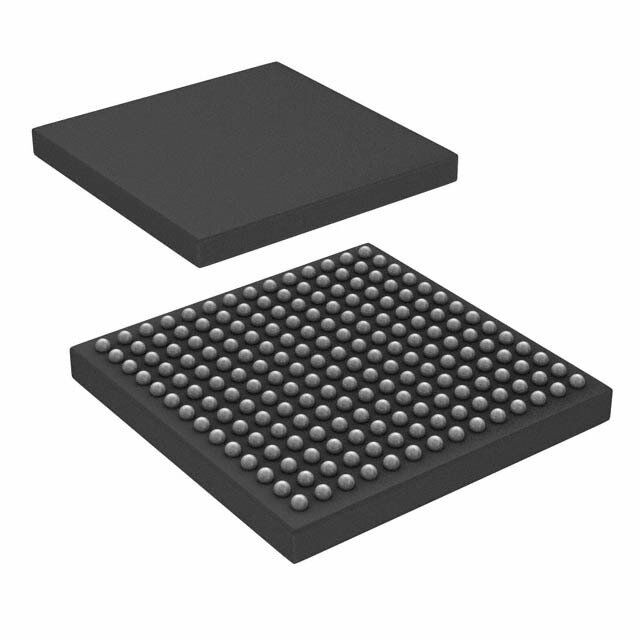
| 供应商器件封装 | 196-BGA MICROSTAR(15x15) |
| 其它名称 | 296-25426 |
| 包装 | 托盘 |
| 单位重量 | 557.300 mg |
| 商标 | Texas Instruments |
| 安装类型 | 表面贴装 |
| 安装风格 | SMD/SMT |
| 封装 | Tray |
| 封装/外壳 | 196-BGA |
| 封装/箱体 | BGA-196 Microstar |
| 工作电源电压 | 3.3 V, 1.5 V |
| 工厂包装数量 | 126 |
| 应用 | PC,PDA |
| 接口 | PCI |
| 数据总线宽度 | 32 bit |
| 最大工作温度 | + 85 C |
| 最大数据速率 | 2 Gbps |
| 最大时钟频率 | 66 MHz |
| 最小工作温度 | - 40 C |
| 标准包装 | 126 |
| 电压-电源 | 1.5V, 3.3V |
| 电源电流—最大值 | 20 mA |
| 端口数量 | 4 Port |
| 类型 | Switch - PCIe |
| 系列 | XIO3130 |
| 通道数 | 4 Lane |


- 商务部:美国ITC正式对集成电路等产品启动337调查
- 曝三星4nm工艺存在良率问题 高通将骁龙8 Gen1或转产台积电
- 太阳诱电将投资9.5亿元在常州建新厂生产MLCC 预计2023年完工
- 英特尔发布欧洲新工厂建设计划 深化IDM 2.0 战略
- 台积电先进制程称霸业界 有大客户加持明年业绩稳了
- 达到5530亿美元!SIA预计今年全球半导体销售额将创下新高
- 英特尔拟将自动驾驶子公司Mobileye上市 估值或超500亿美元
- 三星加码芯片和SET,合并消费电子和移动部门,撤换高东真等 CEO
- 三星电子宣布重大人事变动 还合并消费电子和移动部门
- 海关总署:前11个月进口集成电路产品价值2.52万亿元 增长14.8%


_renders/CS4265-CNZR.jpg)
PDF Datasheet 数据手册内容提取
XIO3130 XIO3130 Data Manual PRODUCTIONDATAinformationiscurrentasofpublicationdate. Products conform to specifications per the terms of the Texas Instruments standard warranty. Production processing does not necessarilyincludetestingofallparameters. LiteratureNumber:SLLS693F May2007–RevisedJanuary2010
XIO3130 SLLS693F–MAY2007–REVISEDJANUARY2010 www.ti.com Contents 1 Features ........................................................................................................................... 11 2 Introduction ...................................................................................................................... 12 2.1 Description ................................................................................................................. 12 2.2 RelatedDocuments ....................................................................................................... 12 2.3 DocumentConventions ................................................................................................... 13 2.4 OrderingInformation ...................................................................................................... 13 2.5 TerminalAssignments .................................................................................................... 14 2.6 TerminalDescriptions ..................................................................................................... 17 3 Description ....................................................................................................................... 22 3.1 Power-Up/Power-DownSequencing .................................................................................... 22 3.1.1 Power-UpSequence ........................................................................................... 22 3.1.2 Power-DownSequence ........................................................................................ 23 3.2 ExpressInterface .......................................................................................................... 23 3.2.1 ExternalReferenceClock ..................................................................................... 23 3.2.2 ClockGenerator ................................................................................................ 23 3.2.3 Beacon ........................................................................................................... 24 3.2.4 WAKE ............................................................................................................ 24 3.2.5 InitialFlowControlCredits .................................................................................... 24 3.2.6 PCIExpressMessageTransactions ......................................................................... 24 3.3 GPIOTerminals............................................................................................................ 25 3.4 SerialEEPROM............................................................................................................ 25 3.4.1 SerialBusInterfaceImplementation ......................................................................... 25 3.4.2 SerialBusInterfaceProtocol .................................................................................. 26 3.4.3 SerialBusEEPROMApplication ............................................................................. 28 3.4.4 AccessingSerialBusDevicesThroughSoftware .......................................................... 31 3.5 SwitchResetFeatures .................................................................................................... 31 4 XIO3130ConfigurationRegisterSpace................................................................................. 33 4.1 PCIConfigurationRegisterSpaceOverview .......................................................................... 33 4.2 PCIExpressUpstreamPortRegisters ................................................................................. 34 4.2.1 PCIConfigurationSpace(UpstreamPort)RegisterMap ................................................. 35 4.2.2 VendorIDRegister ............................................................................................. 36 4.2.3 DeviceIDRegister ............................................................................................. 36 4.2.4 CommandRegisters ........................................................................................... 36 4.2.5 StatusRegister.................................................................................................. 37 4.2.6 ClassCodeandRevisionIDRegister ....................................................................... 39 4.2.7 CacheLineSizeRegister ..................................................................................... 39 4.2.8 PrimaryLatencyTimerRegister .............................................................................. 39 4.2.9 HeaderTypeRegister.......................................................................................... 40 4.2.10 BISTRegister ................................................................................................... 40 4.2.11 PrimaryBusNumber ........................................................................................... 40 4.2.12 SecondaryBusNumber ....................................................................................... 40 4.2.13 SubordinateBusNumber ...................................................................................... 41 4.2.14 SecondaryLatencyTimerRegister .......................................................................... 41 4.2.15 I/OBaseRegister ............................................................................................... 41 4.2.16 I/OLimitRegister ............................................................................................... 42 2 Contents Copyright©2007–2010,TexasInstrumentsIncorporated
XIO3130 www.ti.com SLLS693F–MAY2007–REVISEDJANUARY2010 4.2.17 SecondaryStatusRegister .................................................................................... 42 4.2.18 MemoryBaseRegister......................................................................................... 43 4.2.19 MemoryLimitRegister ......................................................................................... 43 4.2.20 Pre-fetchableMemoryBaseRegister ........................................................................ 43 4.2.21 Pre-FetchableMemoryLimitRegister ....................................................................... 44 4.2.22 Pre-FetchableBaseUpper32BitsRegister ................................................................ 44 4.2.23 Pre-fetchableLimitUpper32BitsRegister ................................................................. 45 4.2.24 I/OBaseUpper16BitsRegister ............................................................................. 45 4.2.25 I/OLimitUpper16BitsRegister .............................................................................. 45 4.2.26 CapabilitiesPointerRegister .................................................................................. 46 4.2.27 InterruptLineRegister ......................................................................................... 46 4.2.28 InterruptPinRegister .......................................................................................... 46 4.2.29 BridgeControlRegister ........................................................................................ 46 4.2.30 CapabilityIDRegister .......................................................................................... 48 4.2.31 Next-ItemPointerRegister .................................................................................... 48 4.2.32 PowerManagementCapabilitiesRegister .................................................................. 48 4.2.33 PowerManagementControl/StatusRegister ............................................................... 49 4.2.34 PowerManagementBridgeSupportExtensionRegister.................................................. 50 4.2.35 PowerManagementDataRegister........................................................................... 50 4.2.36 MSICapabilityIDRegister .................................................................................... 50 4.2.37 Next-ItemPointerRegister .................................................................................... 50 4.2.38 MSIMessageControlRegister ............................................................................... 51 4.2.39 MSIMessageAddressRegister .............................................................................. 51 4.2.40 MSIMessageUpperAddressRegister ...................................................................... 52 4.2.41 MSIMessageDataRegister .................................................................................. 52 4.2.42 CapabilityIDRegister .......................................................................................... 52 4.2.43 Next-ItemPointerRegister .................................................................................... 53 4.2.44 SubsystemVendorIDRegister ............................................................................... 53 4.2.45 SubsystemIDRegister ........................................................................................ 53 4.2.46 PCIExpressCapabilityIDRegister .......................................................................... 53 4.2.47 Next-ItemPointerRegister .................................................................................... 54 4.2.48 PCIExpressCapabilitiesRegister ........................................................................... 54 4.2.49 DeviceCapabilitiesRegister .................................................................................. 54 4.2.50 DeviceControlRegister ....................................................................................... 55 4.2.51 DeviceStatusRegister......................................................................................... 56 4.2.52 LinkCapabilitiesRegister...................................................................................... 57 4.2.53 LinkControlRegister ........................................................................................... 58 4.2.54 LinkStatusRegister ............................................................................................ 59 4.2.55 SerialBusDataRegister ...................................................................................... 59 4.2.56 SerialBusIndexRegister ..................................................................................... 59 4.2.57 SerialBusSlaveAddressRegister........................................................................... 60 4.2.58 SerialBusControlandStatusRegister...................................................................... 60 4.2.59 UpstreamPortLinkPMLatencyRegister ................................................................... 61 4.2.60 GlobalChipControlRegister.................................................................................. 63 4.2.61 GPIOAControlRegister ...................................................................................... 64 Copyright©2007–2010,TexasInstrumentsIncorporated Contents 3
XIO3130 SLLS693F–MAY2007–REVISEDJANUARY2010 www.ti.com 4.2.62 GPIOBControlRegister ...................................................................................... 66 4.2.63 GPIOCControlRegister ...................................................................................... 68 4.2.64 GPIODControlRegister ...................................................................................... 70 4.2.65 GPIODataRegister ............................................................................................ 72 4.2.66 TIProprietaryRegister ......................................................................................... 75 4.2.67 TIProprietaryRegister ......................................................................................... 75 4.2.68 TIProprietaryRegister ......................................................................................... 75 4.2.69 TIProprietaryRegister ......................................................................................... 76 4.2.70 TIProprietaryRegister ......................................................................................... 76 4.2.71 TIProprietaryRegister ......................................................................................... 76 4.2.72 SubsystemAccessRegister .................................................................................. 77 4.2.73 GeneralControlRegister ...................................................................................... 77 4.2.74 DownstreamPortsLinkPMLatencyRegister .............................................................. 78 4.2.75 GlobalSwitchControlRegister ............................................................................... 79 4.2.76 AdvancedErrorReportingCapabilityIDRegister .......................................................... 80 4.2.77 NextCapabilityOffset/CapabilityVersionRegister ........................................................ 80 4.2.78 UncorrectableErrorStatusRegister ......................................................................... 80 4.2.79 UncorrectableErrorMaskRegister .......................................................................... 81 4.2.80 UncorrectableErrorSeverityRegister ....................................................................... 82 4.2.81 CorrectableErrorStatusRegister ............................................................................ 83 4.2.82 CorrectableErrorMaskRegister ............................................................................. 84 4.2.83 AdvancedErrorCapabilitiesandControlRegister ......................................................... 85 4.2.84 HeaderLogRegister ........................................................................................... 86 4.3 PCIExpressDownstreamPortRegisters .............................................................................. 87 4.3.1 PCIConfigurationSpace(DownstreamPort)RegisterMap .............................................. 87 4.3.2 VendorIDRegister ............................................................................................. 88 4.3.3 DeviceIDRegister ............................................................................................. 88 4.3.4 CommandRegister ............................................................................................. 88 4.3.5 StatusRegister.................................................................................................. 89 4.3.6 ClassCodeandRevisionIDRegister ....................................................................... 90 4.3.7 CacheLineSizeRegister ..................................................................................... 91 4.3.8 PrimaryLatencyTimerRegister .............................................................................. 91 4.3.9 HeaderTypeRegister.......................................................................................... 91 4.3.10 BISTRegister ................................................................................................... 91 4.3.11 PrimaryBusNumber ........................................................................................... 92 4.3.12 SecondaryBusNumber ....................................................................................... 92 4.3.13 SubordinateBusNumber ...................................................................................... 92 4.3.14 SecondaryLatencyTimerRegister .......................................................................... 92 4.3.15 I/OBaseRegister ............................................................................................... 93 4.3.16 I/OLimitRegister ............................................................................................... 93 4.3.17 SecondaryStatusRegister .................................................................................... 93 4.3.18 MemoryBaseRegister......................................................................................... 94 4.3.19 MemoryLimitRegister ......................................................................................... 95 4.3.20 Pre-fetchableMemoryBaseRegister ........................................................................ 95 4.3.21 Pre-fetchableMemoryLimitRegister ........................................................................ 95 4 Contents Copyright©2007–2010,TexasInstrumentsIncorporated
XIO3130 www.ti.com SLLS693F–MAY2007–REVISEDJANUARY2010 4.3.22 Pre-fetchableBaseUpper32BitsRegister ................................................................. 96 4.3.23 Pre-fetchableLimitUpper32BitsRegister ................................................................. 96 4.3.24 I/OBaseUpper16BitsRegister ............................................................................. 97 4.3.25 I/OLimitUpper16BitsRegister .............................................................................. 97 4.3.26 CapabilitiesPointerRegister .................................................................................. 97 4.3.27 InterruptLineRegister ......................................................................................... 98 4.3.28 InterruptPinRegister .......................................................................................... 98 4.3.29 BridgeControlRegister ........................................................................................ 98 4.3.30 CapabilityIDRegister ........................................................................................ 100 4.3.31 Next-ItemPointerRegister ................................................................................... 100 4.3.32 PowerManagementCapabilitiesRegister ................................................................. 100 4.3.33 PowerManagementControl/StatusRegister.............................................................. 101 4.3.34 PowerManagementBridgeSupportExtensionRegister ................................................ 102 4.3.35 PowerManagementDataRegister ......................................................................... 102 4.3.36 MSICapabilityIDRegister ................................................................................... 102 4.3.37 Next-ItemPointerRegister ................................................................................... 102 4.3.38 MSIMessageControlRegister .............................................................................. 103 4.3.39 MSIMessageAddressRegister ............................................................................ 103 4.3.40 MSIMessageUpperAddressRegister .................................................................... 104 4.3.41 MSIMessageDataRegister ................................................................................. 104 4.3.42 CapabilityIDRegister ........................................................................................ 104 4.3.43 Next-ItemPointerRegister ................................................................................... 106 4.3.44 SubsystemVendorIDRegister ............................................................................. 106 4.3.45 SubsystemIDRegister ....................................................................................... 106 4.3.46 PCIExpressCapabilityIDRegister......................................................................... 106 4.3.47 Next-ItemPointerRegister ................................................................................... 107 4.3.48 PCIExpressCapabilitiesRegister .......................................................................... 107 4.3.49 DeviceCapabilitiesRegister ................................................................................. 107 4.3.50 DeviceControlRegister ...................................................................................... 108 4.3.51 DeviceStatusRegister ....................................................................................... 109 4.3.52 LinkCapabilitiesRegister .................................................................................... 110 4.3.53 LinkControlRegister ......................................................................................... 111 4.3.54 LinkStatusRegister .......................................................................................... 112 4.3.55 SlotCapabilitiesRegister .................................................................................... 112 4.3.56 SlotControlRegister.......................................................................................... 114 4.3.57 SlotStatusRegister ........................................................................................... 116 4.3.58 TIProprietaryRegister ....................................................................................... 117 4.3.59 TIProprietaryRegister ....................................................................................... 117 4.3.60 TIProprietaryRegister ....................................................................................... 118 4.3.61 GeneralControlRegister ..................................................................................... 118 4.3.62 L0sIdleTimeoutRegister .................................................................................... 120 4.3.63 GeneralSlotInfoRegister ................................................................................... 120 4.3.64 AdvancedErrorReportingCapabilitiesIDRegister ...................................................... 121 4.3.65 NextCapabilityOffset/CapabilityVersionRegister ....................................................... 121 4.3.66 UncorrectableErrorStatusRegister ........................................................................ 121 Copyright©2007–2010,TexasInstrumentsIncorporated Contents 5
XIO3130 SLLS693F–MAY2007–REVISEDJANUARY2010 www.ti.com 4.3.67 UncorrectableErrorMaskRegister ......................................................................... 122 4.3.68 UncorrectableErrorSeverityRegister...................................................................... 123 4.3.69 CorrectableErrorStatusRegister........................................................................... 124 4.3.70 CorrectableErrorMaskRegister ............................................................................ 125 4.3.71 AdvancedErrorCapabilitiesandControlRegister ....................................................... 126 4.3.72 HeaderLogRegister.......................................................................................... 126 5 PCIHotPlugImplementationOverview .............................................................................. 128 5.1 PCIHotPlugArchitectureOverview .................................................................................. 128 5.2 PCIHotPlugTiming ..................................................................................................... 130 5.2.1 Power-UpCycle ............................................................................................... 130 5.2.1.1 NonPCIHotPlugPower-UpCycle ............................................................. 130 5.2.1.2 PCIHotPlugPower-UpCycleWithPWRGDnFeedback .................................. 130 5.2.1.3 PCIHotPlugPower-UpCycleWithNoPWRGDnFeedback .............................. 130 5.2.2 Power-DownCycles .......................................................................................... 131 5.2.2.1 NormalPower-Down ............................................................................. 131 5.2.2.2 SurpriseRemoval ................................................................................ 131 5.2.2.3 PWRGDnDe-Assertion .......................................................................... 132 5.2.3 PMI_Turn_OffandPME_To_AckMessages .............................................................. 132 5.2.4 DebounceCircuits ............................................................................................ 133 5.2.5 HP_INTXPin .................................................................................................. 133 6 ElectricalCharacteristics .................................................................................................. 134 6.1 AbsoluteMaximumRatings............................................................................................. 134 6.2 RecommendedOperatingConditions ................................................................................. 134 6.3 PCIExpressDifferentialTransmitterOutputRanges ............................................................... 135 6.4 PCIExpressDifferentialReceiverInputRanges .................................................................... 136 6.5 PCIExpressDifferentialReferenceClockInputRanges ........................................................... 137 6.6 PCIExpressReferenceClockOutputRequirements ............................................................... 138 6.7 3.3-VI/OElectricalCharacteristics .................................................................................... 139 6.8 POWERCONSUMPTION .............................................................................................. 139 6.9 THERMALCHARACTERISTICS ...................................................................................... 139 6 Contents Copyright©2007–2010,TexasInstrumentsIncorporated
XIO3130 www.ti.com SLLS693F–MAY2007–REVISEDJANUARY2010 List of Figures 3-1 BlockDiagram.................................................................................................................... 22 3-2 Power-UpSequenceDiagram.................................................................................................. 23 3-3 Power-DownSequenceDiagram.............................................................................................. 23 3-4 SerialEEPROMApplications................................................................................................... 26 3-5 Serial-BusStart/StopConditionsandBitTransfers.......................................................................... 27 3-6 Serial-BusProtocolAcknowledge.............................................................................................. 27 3-7 Serial-BusProtocol–ByteWrite............................................................................................... 27 3-8 Serial-BusProtocol–ByteRead............................................................................................... 28 3-9 Serial-BusProtocol–Multiple-ByteRead..................................................................................... 28 4-1 XIO3130EnumerationsTopology.............................................................................................. 34 5-1 NonPCIHotPlugPower-UpCycle........................................................................................... 130 5-2 PCIHotPlugPower-UpCycleWithPWFRDnFeedback................................................................. 130 5-3 PCIHotPlugPower-UpCycleWithNoPWGRDnFeedback ............................................................ 131 5-4 NormalPower-Down........................................................................................................... 131 5-5 SurpriseRemoval............................................................................................................... 132 5-6 EffectWhenPWFRGnGoesLow............................................................................................ 132 Copyright©2007–2010,TexasInstrumentsIncorporated ListofFigures 7
XIO3130 SLLS693F–MAY2007–REVISEDJANUARY2010 www.ti.com List of Tables 2-1 XIO3130TerminalAssignments................................................................................................ 14 2-2 XIO3130TerminalsSortedAlphanumerically................................................................................ 15 2-3 XIO3130SignalNamesSortedAlphabetically............................................................................... 16 2-4 PowerSupplyTerminals ........................................................................................................ 17 2-5 CombinedPowerTerminals.................................................................................................... 17 2-6 GroundTerminals................................................................................................................ 18 2-7 PCIExpressReferenceClockTerminals..................................................................................... 18 2-8 PCIExpressTerminals.......................................................................................................... 19 2-9 PCIHotPlugStrappingTerminals............................................................................................. 19 2-10 GPIOTerminals.................................................................................................................. 20 2-11 MiscellaneousTerminals........................................................................................................ 21 3-1 InitialFlowControlCreditAdvertisements.................................................................................... 24 3-2 MessagesSupportedbytheXIO3130......................................................................................... 25 3-3 EEPROMRegisterLoadingMap............................................................................................... 29 3-4 RegisterforProgrammingSerial-BusDevices............................................................................... 31 3-5 SwitchResetOptions............................................................................................................ 32 4-1 PCIExpressUpstreamPortConfigurationRegisterMap(Type1)........................................................ 35 4-2 ExtendedConfigurationSpace(UpstreamPort)............................................................................. 36 4-3 BitDescriptions–CommandRegister ........................................................................................ 37 4-4 BitDescriptions–StatusRegister............................................................................................. 38 4-5 BitDescriptions–ClassCodeandRevisionIDRegister .................................................................. 39 4-6 BitDescriptions–I/OBaseRegister .......................................................................................... 41 4-7 BitDescriptions–I/OLimitRegister .......................................................................................... 42 4-8 BitDescriptions–SecondaryStatusRegister ............................................................................... 42 4-9 BitDescriptions–MemoryBaseRegister.................................................................................... 43 4-10 BitDescriptions–MemoryLimitRegister .................................................................................... 43 4-11 BitDescriptions–Pre-fetchableMemoryBaseRegister ................................................................... 44 4-12 BitDescriptions–Pre-fetchableMemoryLimitRegister ................................................................... 44 4-13 BitDescriptions–Pre-fetchableBaseUpper32BitsRegister ............................................................ 44 4-14 BitDescriptions–Pre-fetchableLimitUpper32BitsRegister ............................................................ 45 4-15 BitDescriptions–I/OBaseUpper16BitsRegister ........................................................................ 45 4-16 BitDescriptions–I/OLimitUpper16BitsRegister ......................................................................... 45 4-17 BitDescriptions–BridgeControlRegister ................................................................................... 47 4-18 BitDescriptions–PowerManagementCapabilitiesRegister ............................................................. 48 4-19 BitDescriptions–PowerManagementControl/StatusRegister .......................................................... 49 4-20 BitDescriptions–PMBridgeSupportExtensionRegister ................................................................. 50 4-21 BitDescriptions–MSIMessageControlRegister .......................................................................... 51 4-22 BitDescriptions–MSIMessageAddressRegister ......................................................................... 52 4-23 BitDescriptions–MSIDataRegister ......................................................................................... 52 4-24 BitDescriptions–PCIExpressCapabilitiesRegister ...................................................................... 54 4-25 BitDescriptions–DeviceCapabilitiesRegister ............................................................................. 55 4-26 BitDescriptions–DeviceControlRegister .................................................................................. 55 4-27 BitDescriptions–DeviceStatusRegister.................................................................................... 57 4-28 BitDescriptions–LinkCapabilitiesRegister................................................................................. 57 4-29 BitDescriptions–LinkControlRegister ...................................................................................... 58 4-30 BitDescriptions–LinkStatusRegister ....................................................................................... 59 8 ListofTables Copyright©2007–2010,TexasInstrumentsIncorporated
XIO3130 www.ti.com SLLS693F–MAY2007–REVISEDJANUARY2010 4-31 BitDescriptions–SerialBusSlaveAddressRegister...................................................................... 60 4-32 BitDescriptions–SerialBusControlandStatusRegister................................................................. 60 4-33 BitDescriptions–UpstreamPortLinkPMLatencyRegister .............................................................. 62 4-34 BitDescriptions–GlobalChipControlRegister............................................................................. 63 4-35 BitDescriptions–GPIOAControlRegister ................................................................................. 65 4-36 BitDescriptions–GPIOBControlRegister ................................................................................. 67 4-37 BitDescriptions–GPIOCControlRegister ................................................................................. 69 4-38 BitDescriptions–GPIODControlRegister.................................................................................. 71 4-39 BitDescriptions–GPIODataRegister........................................................................................ 72 4-40 BitDescriptions–SubsystemAccessRegister ............................................................................. 77 4-41 BitDescriptions–GeneralControlRegister ................................................................................. 77 4-42 BitDescriptions–DownstreamPortsLinkPMLatencyRegister ......................................................... 78 4-43 BitDescriptions–GlobalSwitchControlRegister .......................................................................... 79 4-44 UncorrectableErrorStatusRegister .......................................................................................... 81 4-45 UncorrectableErrorMaskRegister ........................................................................................... 81 4-46 UncorrectableErrorSeverityRegister ........................................................................................ 83 4-47 CorrectableErrorStatusRegister ............................................................................................. 84 4-48 CorrectableErrorMaskRegister .............................................................................................. 84 4-49 AdvancedErrorCapabilitiesandControlRegister .......................................................................... 85 4-50 PCIExpressDownstreamPortConfigurationRegisterMap(Type1).................................................... 87 4-51 ExtendedConfigurationSpace(DownstreamPort).......................................................................... 88 4-52 BitDescriptions–CommandRegister ........................................................................................ 89 4-53 BitDescriptions–StatusRegister............................................................................................. 89 4-54 BitDescriptions–ClassCodeandRevisionIDRegister .................................................................. 90 4-55 BitDescriptions–I/OBaseRegister .......................................................................................... 93 4-56 BitDescriptions–I/OLimitRegister .......................................................................................... 93 4-57 BitDescriptions–SecondaryStatusRegister ............................................................................... 94 4-58 IBitDescriptions–MemoryBaseRegister ................................................................................... 94 4-59 BitDescriptions–MemoryLimitRegister .................................................................................... 95 4-60 Descriptions–Pre-fetchableMemoryBaseRegister....................................................................... 95 4-61 BitDescriptions–Pre-fetchableMemoryLimitRegister ................................................................... 96 4-62 BitDescriptions–Pre-fetchableBaseUpper32BitsRegister ............................................................ 96 4-63 Descriptions–Pre-fetchableLimitUpper32BitsRegister ................................................................ 96 4-64 BitDescriptions–I/OBaseUpper16BitsRegister ........................................................................ 97 4-65 BitDescriptions–I/OLimitUpper16BitsRegister ......................................................................... 97 4-66 BitDescriptions–BridgeControlRegister ................................................................................... 98 4-67 BitDescriptions–PowerManagementCapabilitiesRegister ............................................................ 100 4-68 BitDescriptions–PowerManagementControl/StatusRegister......................................................... 101 4-69 BitDescriptions–PMBridgeSupportExtensionRegister ............................................................... 102 4-70 BitDescriptions–MSIMessageControlRegister ......................................................................... 103 4-71 BitDescriptions–MSIMessageAddressRegister ....................................................................... 104 4-72 BitDescriptions–MSIDataRegister ....................................................................................... 104 4-73 BitDescriptions–PCIExpressCapabilitiesRegister ..................................................................... 107 4-74 BitDescriptions–DeviceCapabilitiesRegister ............................................................................ 108 4-75 BitDescriptions–DeviceControlRegister ................................................................................. 108 4-76 BitDescriptions–DeviceStatusRegister .................................................................................. 110 4-77 BitDescriptions–LinkCapabilitiesRegister ............................................................................... 110 4-78 BitDescriptions–LinkControlRegister .................................................................................... 111 Copyright©2007–2010,TexasInstrumentsIncorporated ListofTables 9
XIO3130 SLLS693F–MAY2007–REVISEDJANUARY2010 www.ti.com 4-79 BitDescriptions–LinkStatusRegister ..................................................................................... 112 4-80 BitDescriptions–SlotCapabilitiesRegister ............................................................................... 113 4-81 BitDescriptions–SlotControlRegister..................................................................................... 114 4-82 BitDescriptions–SlotStatusRegister...................................................................................... 116 4-83 BitDescriptions–GeneralControlRegister................................................................................ 118 4-84 BitDescriptions–GeneralSlotInfoRegister .............................................................................. 121 4-85 UncorrectableErrorStatusRegister......................................................................................... 122 4-86 UncorrectableErrorMaskRegister .......................................................................................... 122 4-87 UncorrectableErrorSeverityRegister ...................................................................................... 124 4-88 CorrectableErrorStatusRegister ........................................................................................... 125 4-89 CorrectableErrorMaskRegister ............................................................................................. 125 4-90 AdvancedErrorCapabilitiesandControlRegister ........................................................................ 126 5-1 GPIOMatrix..................................................................................................................... 128 5-2 PCIHotPlugSidebandSignals............................................................................................... 129 5-3 PinsAssignedtoGPIOControlRegisters................................................................................... 129 10 ListofTables Copyright©2007–2010,TexasInstrumentsIncorporated
XIO3130 www.ti.com SLLS693F–MAY2007–REVISEDJANUARY2010 XIO3130 CheckforSamples:XIO3130 1 Features 12 • PCIExpressBaseSpecification,Revision1.1 • SupportforD1,D2,D3hot,andD3cold • PCIExpressCardElectromechanical • ActiveStatePowerManagement(ASPM)Using Specification,Revision1.1 BothL0sandL1 • PCI-to-PCIBridgeArchitectureSpecification, • Low-PowerPCIExpressTransmitterMode Revision1.1 • IntegratedAUXPowerSwitchDrainsVAUX • PCIBusPowerManagementInterface PowerOnlyWhenMainPowerIsOff Specification,Revision1.2 • IntegratedPCIHotPlugSupport • PCIExpressFanoutSwitchWithOne×1 • IntegratedREFCLKBuffersforSwitch UpstreamPortandThree×1DownstreamPorts DownstreamPorts • PacketTransmissionStartsWhileReception • 3.3-VMultifunctionI/OPinsforPCIHotPlug StillinProgress(Cut-Through) StatusandControlorGeneralPurposeI/Os • 256-ByteMaximumDataPayloadSize • OptionalSerialEEPROMforSystem-Specific • Peer-to-PeerSupport ConfigurationRegisterInitialization • WakeEventandBeaconSupport 1 Pleasebeawarethatanimportantnoticeconcerningavailability,standardwarranty,anduseincriticalapplicationsofTexas Instrumentssemiconductorproductsanddisclaimerstheretoappearsattheendofthisdatasheet. PCIExpress,PCIHotPlugaretrademarksofothers. 2 PRODUCTIONDATAinformationiscurrentasofpublicationdate. Copyright©2007–2010,TexasInstrumentsIncorporated Products conform to specifications per the terms of the Texas Instruments standard warranty. Production processing does not necessarilyincludetestingofallparameters.
XIO3130 SLLS693F–MAY2007–REVISEDJANUARY2010 www.ti.com 2 Introduction The Texas Instruments XIO3130 switch is an integrated PCI Express fanout switch solution with one upstream x1 port and three downstream x1 ports. This high-performance integrated solution provides the latest in PCI Express switch technology including cut-through architecture, integrated reference clock buffers for downstream ports, integrated main power/V power switch, and downstream port PCI Hot AUX Plug®support. The reader is assumed to have prior knowledge of the PCI Express interface and associated terminology andofthePCI-SIGspecifications. 2.1 Description TheTexasInstrumentsXIO3130switchisaPCIExpress×13-portfanoutswitch.TheXIO3130providesa single x1 upstream port supporting full 250-MB/s packet throughput in each direction simultaneously. Three independently configurable ×1 downstream ports are provided that also support full 250-MB/s packetthroughputineachdirectionsimultaneously. A cut-through architecture is implemented to reduce the latency associated with packets moving through the PCI Express fabric. As soon as the address or routing information is decoded within the header of a packet entering an ingress port, the packet is directed to the egress port for forwarding. Packet poisoning using the EDB framing signal is supported in circumstances where packet errors are detected after the transmissionoftheegresspacketbegins. The downstream ports may be configured to support PCI Hot Plug slot implementations. In this scenario, the system designer may decide to use the integrated PCI Hot Plug-compliant controller. This feature is available through the classic PCI configuration space under the PCI Express Capability Structure. When enabled, the downstream ports provide the PCI Hot Plug standard mechanism to apply and remove power totheslotorsocket. Power-management features include Active State Power Management, PME mechanisms, the Beacon/Wake protocol, and all conventional PCI D-states. When ASPM is enabled, each link automatically saves power when idle using the L0s and L1 states. PME messages are supported along withthePME_Turn_Off/PME_TO_Ackprotocol. When enabled, the upstream port supports Beacon transmission as well as the WAKE side band signal to wake the system as the result of a PCI Hot Plug event. Furthermore, the downstream ports may be configured to detect Beacon from downstream devices and forward this upstream. The switch also supports the translation and forwarding of WAKE from a downstream device into Beacon on the upstream portforcabledimplementations. 2.2 Related Documents Trademarks 12 Introduction Copyright©2007–2010,TexasInstrumentsIncorporated SubmitDocumentationFeedback ProductFolderLink(s):XIO3130
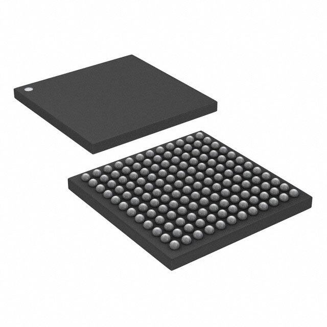
XIO3130 www.ti.com SLLS693F–MAY2007–REVISEDJANUARY2010 2.3 Document Conventions Throughout this data manual, several conventions are used to convey information. These conventions are listedbelow: 1. Toidentifyabinarynumberorfield,alowercasebfollowsthenumbers.Forexample:000bisa3-bit binaryfield. 2. Toidentifyahexadecimalnumberorfield,alowercasehfollowsthenumbers.Forexample:8AFhisa 12-bithexadecimalfield. 3. Allothernumbersthatappearinthisdocumentthatdonothaveeitheraborhfollowingthenumber areassumedtobedecimalformat. 4. Ifthesignalorterminalnamehasabarabovethename(forexample,GRST),thenthisindicatesthe logicalNOTfunction.Whenasserted,thissignalisalogiclow,0,or0b. 5. DifferentialsignalnamesendwithP,N,+,or– designators.ThePor+designatorssignifythepositive signalassociatedwiththedifferentialpair.TheNor–designatorssignifythenegativesignal associatedwiththedifferentialpair. 6. RSVDindicatesthatthereferenceditemisreserved. 7. InSections4through6,theconfigurationspaceforthebridgeisdefined.Foreachregisterbit,the software-accessmethodisidentifiedinanaccesscolumn.Thelegendforthisaccesscolumnincludes thefollowingentries: – r– readaccessbysoftware – u –updatesbythebridgeinternalhardware – w– writeaccessbysoftware – c– clearanassertedbitwithawrite-backof1bbysoftware.Writeofzerotothefieldhasnoeffect – s– thefieldmaybesetbyawriteofone.Writeofzerotothefieldhasnoeffect. – na– notaccessibleornotapplicable 2.4 Ordering Information ORDERINGNUMBER TEMPERATURE PACKAGE XIO3130 0°Cto70°C 196-terminalZHC XIO3130I –40°Cto85°C Copyright©2007–2010,TexasInstrumentsIncorporated Introduction 13 SubmitDocumentationFeedback ProductFolderLink(s):XIO3130
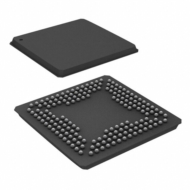
XIO3130 SLLS693F–MAY2007–REVISEDJANUARY2010 www.ti.com 2.5 Terminal Assignments TheXIO3130ispackagedina196-ballZHCMicroStar™BGA. Table2-1.XIO3130TerminalAssignments A B C D E F G H J K L M N P VSSA DN2_ VSSA DN2_ DN2_ DN2_ 14 GPIO12 SCL VDD15 GPIO4 VDD15 GPIO15 VDD15 VDD15 (2) PERn (2) Petn REFCKOn REFCKOp DN2_ DN2_ VSSA VSSA DN2_ 13 RSVD GPIO13 VDD15 SDA VDD15 VDD15 GPIO6 VDD15 GPIO7 PERp PETp (2) (2) DPSTRP VSSA VDDA15 VSSA VDDA15 12 GPIO2 RSVD GPIO3 VDD33 VSS VDD33 GPIO5 VDD15 GPIO14 GPIO16 (2) (2) (2) (2) VSSA VDDA15 VDDA15 VDDA15 11 VDD33 GPIO1 VDD15 VSS VSS VSS VSS VDD15 GPIO11 VDD33 (2) (2) (2) (2) VSSA DN1_ VSSA 10 VDD15 VSS VSS VSS VSS VSS VSS VSS VSS GPIO8 VDD15 (1) DPSTRP (3) DN1_ DN1_ VSSA VDDA15 VSSA VSSA DN3_ DN3_ 9 REFCK REFCK VSS VSS VSS VSS VSS VSS (1) (1) (3) (3) PERp PERn Op On DN1_ DN1_ VSSA VDDA15 VDDA15 VDDA15 VSSA 8 VSS VSS VSS VSS VSS VSS VDD15 PETp PETn (1) (1) (3) (3) (3) VDDA15 VSSA VDDA15 VDDA15 VSSA DN3_ DN3_ 7 VDD15 VSS VSS VSS VSS VSS VSS (1) (1) (1) (3) (3) PETp PETn DN1_ DN1_ VDDA15 VDDA15 VSSA DN3_ 6 GPIO0 VSS VSS VSS VSS VSS VSS VSS PERp PERn (3) (3) (3) REFCKOn VSSA DN1_ VSSA DN3_ 5 VDD15 VSS VSS VSS VSS VSS VSS VSS VSS VSS (1) PERST (3) REFCKOp VDD VSSA VDDA15 VDDA15 VDDA15 DN3_ 4 VDD15 VDD33 RSVD RSVD COMB VDD15 VSS VDD33 VDD15 REF (0) (0) (0) DPSTRP 33 VDD VDD15 VSSA VDDA15 3 VDD33 VDD15 WAKE REFR1 VDD15 VDDA33 GPIO18 GPIO17 GPIO9 VDD15 COMBIO REF (0) (0) DN2_ VDD33 UP_ VDDA15 UP_ UP_ CLKREQ 2 VDD15 GRST REFR0 VDD15 VSS VDD15 GPIO10 PERST REF PETn (0) PERn REFCKIn _UP DN3_ UP_ VDD VSSD VAUX33 UP_ VSSA UP_ VSSA UP_ 1 VDD15 VDD15 VDD33 RSVD PERST PERST COMB15 REF REF PETp (0) PERp (0) REFCKIp 14 Introduction Copyright©2007–2010,TexasInstrumentsIncorporated SubmitDocumentationFeedback ProductFolderLink(s):XIO3130
XIO3130 www.ti.com SLLS693F–MAY2007–REVISEDJANUARY2010 Table2-2.XIO3130TerminalsSortedAlphanumerically Ball SignalName Ball SignalName Ball SignalName Ball SignalName Ball SignalName A01 DN3_PERST C13 VDD15 F11 VSSA(2) J08 VSS M06 VDDA15(3) A02 DN2_PERST C14 VDD15 F12 VSSA(2) J09 VSS M07 VSSA(3) A03 VDD33 D01 VSSDREF F13 DN2_PERp J10 VSS M08 VDDA15(3) A04 VDD15 D02 REFR0 F14 DN2_PERn J11 VDDA15(2) M09 VSSA(3) A05 VSSA(1) D03 VDDCOMBIO G01 UP_PETp J12 VDDA15(2) M10 GPIO8 A06 DN1_PERp D04 RSVD G02 UP_PETn J13 VSSA(2) M11 VDD15 A07 VDDA15(1) D05 VSS G03 VSSA(0) J14 DN2_REFCKOn M12 VDD15 A08 DN1_PETp D06 VSS G04 VDDA15(0) K01 VSSA(0) M13 GPIO6 A09 DN1_REFCKOp D07 VDDA15(1) G05 VSS K02 VSS M14 GPIO15 A10 VSSA(1) D08 VDDA15(1) G06 VSS K03 VDDA15(0) N01 VDD33 A11 VDD33 D09 VDDA15(1) G07 VSS K04 VDD15 N02 CLKREQ_UP A12 GPIO2 D10 VSS G08 VSS K05 VSS N03 GPIO9 A13 RSVD D11 VSS G09 VSS K06 VSS N04 DN3_DPSTRP A14 GPIO12 D12 VDD33 G10 VSS K07 VSS N05 VSSA(3) B01 UP_PERST D13 SDA G11 VDDA15(2) K08 VSS N06 VSSA(3) B02 VDD15 D14 GPIO4 G12 VDDA15(2) K09 VSS N07 DN3_PETp B03 VDD15 E01 VAUX33REF G13 VDD15 K10 VSS N08 VDD15 B04 VDD33 E02 VDD33REF G14 VSSA(2) K11 VSS N09 DN3_PERp B05 DN1_PERST E03 REFR1 H01 VSSA(0) K12 VDD33 N10 VDD15 B06 DN1_PERn E04 VSSAREF H02 VDDA15(0) K13 VSSA(2) N11 GPIO11 B07 VDD15 E05 VSS H03 VDD15 K14 DN2_REFCKOp N12 GPIO14 B08 DN1_PETn E06 VSS H04 VDDA15(0) L01 UP_REFCKIp N13 VDD15 B09 DN1_REFCKOn E07 VSS H05 VSS L02 UP_REFCKIn N14 VDD15 B10 VDD15 E08 VSS H06 VSS L03 GPIO18 P01 RSVD B11 GPIO1 E09 VSS H06 VSS L04 VSS P02 GPIO10 B12 RSVD E10 VSS H07 VSS L05 VSS P03 VDD15 B13 GPIO13 E11 VSS H08 VSS L06 VDDA15(3) P04 VDD15 B14 SCL E12 VSS H09 VSS L07 VDDA15(3) P05 DN3_REFCKOp C01 VDDCOMB15 E13 VDD15 H10 VSS L08 VDDA15(3) P06 DN3_REFCKOn C02 GRST E14 VSSA(2) H11 VDDA15(2) L09 VSSA(3) P07 DN3_PETn C03 WAKE F01 VDD15 H12 VSSA(2) L10 VSS P08 VSSA(3) C04 RSVD F02 VDD15 H13 DN2_PETp L11 VSS P09 DN3_PERn C05 VDD15 F03 VDD15REF H14 DN2_PETn L12 GPIO5 P10 VSSA(3) C06 GPIO0 F04 VDDCOMB33 J01 UP_PERp L13 DN2_DPSTRP P11 VDD33 C07 VSSA(1) F05 VSS J02 UP_PERn L14 VDD15 P12 GPIO16 C08 VSSA(1) F06 VSS J03 VDDA33 M01 VDD15 P13 GPIO7 C09 VSSA(1) F07 VSS J04 VDDA15(0) M02 VDD15 P14 VDD15 C10 DN1_DPSTRP F08 VSS J05 VSS M03 GPIO17 C11 VDD15 F09 VSS J06 VSS M04 VDD33 C12 GPIO3 F10 VSS J07 VSS M05 VSS Copyright©2007–2010,TexasInstrumentsIncorporated Introduction 15 SubmitDocumentationFeedback ProductFolderLink(s):XIO3130
XIO3130 SLLS693F–MAY2007–REVISEDJANUARY2010 www.ti.com Table2-3.XIO3130SignalNamesSortedAlphabetically SignalName Ball SignalName Ball CLKREQ_UP N02 GPIO5 L12 DN1_DPSTRP C10 GPIO6 M13 DN1_PERn B06 GPIO7 P13 DN1_PERp A06 GPIO8 M10 DN1_PERST B05 GPIO9 N03 DN1_PETn B08 GRST C02 DN1_PETp A08SuggestedProgramValue REFR0 D02 DN1_REFCKOn B09 REFR1 E03 DN1_REFCKOp A09 RSVD A13,B12,C04,D04,P01 DN2_DPSTRP L13 SCL B14 DN2_PERn F14 SDA D13 DN2_PERp F13 UP_PERn J02 DN2_PERST A02 UP_PERp J01 DN2_PETn H14 UP_PERST B01 DN2_PETp H13 UP_PETn G02 DN2_REFCKOn J14 UP_PETp G01 DN2_REFCKOp K14 UP_REFCKIn L02 DN3_DPSTRP N04 UP_REFCKIp L01 DN3_PERn P09 VAUX33REF E01 A04,B02,B03,B07,B10,C05,C11,C13, C14,E13,F01,F02,G13,H03,K04,L14, DN3_PERp N09 VDD15 M01,M02,M11,M12,N08,N10,N13,N14, P03,P04,P14 DN3_PERST A01 VDDA15(0) G04,H02,H04,J04,K03 DN3_PETn P07 VDDA15(1) A07,D07,D08,D09 DN3_PETp N07 VDDA15(2) G11,G12,H11,J11,J12 DN3_REFCKOn P06 VDDA15(3) L06,L07,L08,M06,M08 DN3_REFCKOp P05 VDD15REF F03 GPIO0 C06 VDD33 A03,A11,B04,D12,K12,M04,N01,P11 GPIO1 B11 VDD33REF E02 GPIO10 P02 VDDA33 J03 GPIO11 N11 VDDCOMB15 C01 GPIO12 A14 VDDCOMB33 F04 GPIO13 B13 VDDCOMBIO D03 D05,D06,D10,D11,E05,E06,E07,E08, E09,E10,E11,E12,F05,F06,F07,F08, F09,F10,G05,G06,G07,G08,G09,G10, GPIO14 N12 VSS H05,H06,H07,H08,H09,H10,J05,J06, J07,J08,J09,J10,K02,K05,K06,K07, K08,K09,K10,K11,L04,L05,L10,L11, M05 GPIO15 M14 VSSA(0) G03,H01,K01 GPIO16 P12 VSSA(1) A05,A10,C07,C08,C09 GPIO17 M03 VSSA(2) E14,F11,F12,G14,H12,J13,K13 GPIO18 L03 VSSA(3) L09,M07,M09,N05,N06,P08,P10 GPIO2 A12 VSSAREF E04 GPIO3 C12 VSSDREF D01 GPIO4 D14 WAKE C03 16 Introduction Copyright©2007–2010,TexasInstrumentsIncorporated SubmitDocumentationFeedback ProductFolderLink(s):XIO3130
XIO3130 www.ti.com SLLS693F–MAY2007–REVISEDJANUARY2010 2.6 Terminal Descriptions Table2-4.PowerSupplyTerminals Signal Ball I/OType Externalparts Description G04,H02,H04,J04, 1.5-VanalogpowerterminalsforPCI-Expressupstreamport VDDA15(0) PWR Filter K03 0 1.5-VanalogpowerterminalsforPCI-Expressdownstream VDDA15(1) A07,D07,D08,D09 PWR Filter port1 1.5-VanalogpowerterminalsforPCI-Expressdownstream VDDA15(2) G11,G12,H11,J11,J12 PWR Filter port2 1.5-VanalogpowerterminalsforPCI-Expressdownstream VDDA15(3) L06,L07,L08,M06,M08 PWR Filter port3 A04,B02,B03,B07, B10,C05,C11,C13, C14,E13,F01,F02, Bypass VDD15 G13,H03,K04,L14, PWR 1.5-Vdigitalcorepowerterminals capacitors M01,M02,M11,M12, N08,N10,N13,N14, P03,P04,P14 A03,A11,B04,D12, Bypass VDD33 PWR 3.3-VdigitalI/Opowerterminals K12,M04,N01,P11 capacitors VDDA33 J03 PWR Filter 3.3-Vanalogpowerterminal Bypass VAUX33REF E01 PWR 3.3-VdigitalV powerterminal capacitors AUX VDD15REF F03 PWR Filter 1.5-VPCI-Expressreferencepowerterminal VDD33REF E02 PWR Filter 3.3-VPCI-Expressreferencepowerterminal Table2-5.CombinedPowerTerminals Signal Ball I/OType ExternalParts Description Internallycombined3.3-VmainandV poweroutputforexternal AUX bypasscapacitorfiltering.Suppliesallinternal3.3-Vinputandoutput VDDCOMBIO D03 Passive Bypasscapacitors circuitrypoweredduringD3cold.Caution:Donotusethisterminalto supplyexternalpowertootherdevices. Internallycombined3.3-VmainandV poweroutputforexternal AUX bypasscapacitorfiltering.Suppliesallinternal3.3-Vcircuitrypowered VDDCOMB33 F04 Passive Bypasscapacitors duringD3cold.Caution:Donotusethisterminaltosupplyexternal powertootherdevices. Internallycombined1.5-VmainandV poweroutputforexternal AUX bypasscapacitorfiltering.Suppliesallinternal1.5-Vcircuitrypowered VDDCOMB15 C01 Passive Bypasscapacitors duringD3cold.Caution:Donotusethisterminaltosupplyexternal powertootherdevices. Copyright©2007–2010,TexasInstrumentsIncorporated Introduction 17 SubmitDocumentationFeedback ProductFolderLink(s):XIO3130
XIO3130 SLLS693F–MAY2007–REVISEDJANUARY2010 www.ti.com Table2-6.GroundTerminals Signal Ball I/OType Description D05,D06,D10,D11,E05, E06,E07,E08,E09,E10, E11,E12,F05,F06,F07, F08,F09,F10,G05,G06, G07,G08,G09,G10, VSS GND Digitalgroundterminals H05,H06,H07,H08,H09, H10,J05,J06,J07,J08, J09,J10,K02,K05,K06, K07,K08,K09,K10,K11, L04,L05,L10,L11,M05 VSSA(0) G03,H01,K01 GND AnaloggroundterminalsforupstreamPort0 VSSA(1) A05,A10,C07,C08,C09 GND AnaloggroundterminalsfordownstreamPort1 E14,F11,F12,G14,H12, VSSA(2) GND AnaloggroundterminalsfordownstreamPort2 J13,K13 L09,M07,M09,N05,N06, VSSA(3) GND AnaloggroundterminalsfordownstreamPort3 P08,P10 VSSAREF E04 GND 1.5-VPCI-Expressanalogreferencegroundterminal VSSDREF D01 GND 1.5-VPCI-Expressdigitalreferencegroundterminal Table2-7.PCIExpressReferenceClockTerminals Signal Ball I/OType ExternalParts Description UP_REFCKIp L01 Referenceclockinputs.REFCKIpandREFCKIncomprisethe HSDIFFIN UP_REFCKIn L02 differentialinputpairforthe100-MHzsystemreferenceclock. DN1_REFCKOp A09 HSDIFFOUT 100MHzdifferentialreferenceclockoutputsfordownstreamport1 DN1_REFCKOn B09 DN2_REFCKOp K14 HSDIFFOUT 100MHzdifferentialreferenceclockoutputsfordownstreamport2 DN2_REFCKOn J14 DN3_REFCKOp P05 HSDIFFOUT 100MHzdifferentialreferenceclockoutputsfordownstreamport3 DN3_REFCKOn P06 18 Introduction Copyright©2007–2010,TexasInstrumentsIncorporated SubmitDocumentationFeedback ProductFolderLink(s):XIO3130
XIO3130 www.ti.com SLLS693F–MAY2007–REVISEDJANUARY2010 Table2-8.PCIExpressTerminals Signal Ball I/OType ExternalParts Description UP_PETp G01 HSDIFF Seriescapacitors High-speeddifferentialtransmitpairforupstreamport0 UP_PETn G02 OUT DN1_PETp A08 HSDIFF Seriescapacitors High-speeddifferentialtransmitpairfordownstreamport1 DN1_PETn B08 OUT DN2_PETp H13 HSDIFF Seriescapacitors High-speeddifferentialtransmitpairfordownstreamport2 DN2_PETn H14 OUT DN3_PETp N07 HSDIFF Seriescapacitors High-speeddifferentialtransmitpairfordownstreamport3 DN3_PETn P07 OUT UP_PERp J01 HSDIFFIN High-speeddifferentialreceiverpairforupstreamport0 UP_PERn J02 DN1_PERp A06 HSDIFFIN High-speeddifferentialreceiverpairfordownstreamport1 DN1_PERn B06 DN2_PERp F13 HSDIFFIN High-speeddifferentialreceiverpairfordownstreamport2 DN2_PERn F14 DN3_PERp N09 HSDIFFIN High-speeddifferentialreceiverpairfordownstreamport3 DN3_PERn P09 REFR0 D02 Externalbias ExternalreferenceresistorterminalsforsettingTXdrivercurrent.An Passive REFR1 E03 resistor externalresistorisconnectedbetweentheseterminals. PCI-Express reset input. When logic high, the PERST signal System-side identifies that the system power is stable. When logic low, the UP_PERST B01 LVCMOSIN pullupresistor PERSTsignalgeneratesaninternalpower-onreset. Note:TheUP_PERSTinputbufferhashysteresis. DN1_PERST B05 LVCMOSO Pulldownresistor PCI-Expressresetoutputfordownstreamport1. DN2_PERST A02 LVCMOSO Pulldownresistor PCI-Expressresetoutputfordownstreamport2. DN3_PERST A01 LVCMOSO Pulldownresistor PCI-Expressresetoutputfordownstreamport3. WAKE is an active low signal that is driven low to reactivate the System-side PCI-Expresslinkhierarchy’smainpowerrailsandreferenceclocks. WAKE C03 LVCMOSI/O pullupresistor Note: Since WAKE is an open-drain output buffer, a system-side pullupresistorisrequired. Table2-9.PCIHotPlugStrappingTerminals Signal Ball I/OType ExternalParts Description DownstreamPort1Strap.Thispinispulledhighatthede-assertionof reset.GPIO0,GPIO1,andGPIO2areusedasPCIHotPlugterminals DN1_DPSTR Pulluporpulldown fordownstreamport1andarenolongeravailableforuseasGPIOs. C10 LVCMOSIN P resistor ThethreeterminalsbecomePRESENT,PWR_ON,andPWR_GOOD respectively.TheseGPIOsareavailablefornormaluseifthisterminal ispulledlowatthede-assertionofreset. DownstreamPort2Strap.Thispinispulledhighatthede-assertionof reset.GPIO4,GPIO5,andGPIO6areusedasPCIHotPlugterminals DN2_DPSTR Pulluporpulldown fordownstreamport2andarenolongeravailableforuseasGPIOs. L13 LVCMOSIN P resistor ThethreeterminalsbecomePRESENT,PWR_ON,andPWR_GOOD respectively.TheseGPIOsareavailablefornormaluseifthisterminal ispulledlowatthede-assertionofreset. DownstreamPort3Strap.Thispinispulledhighatthede-assertionof reset.GPIO8,GPIO9,andGPIO10areusedasPCIHotPlugterminals DN3_DPSTR Pulluporpulldown fordownstreamport3andarenolongeravailableforuseasGPIOs. N04 LVCMOSIN P resistor ThethreeterminalsbecomePRESENT,PWR_ON,andPWR_GOOD respectively.TheseGPIOsareavailablefornormaluseifthisterminal ispulledlowatthede-assertionofreset. Copyright©2007–2010,TexasInstrumentsIncorporated Introduction 19 SubmitDocumentationFeedback ProductFolderLink(s):XIO3130
XIO3130 SLLS693F–MAY2007–REVISEDJANUARY2010 www.ti.com Table2-10.GPIOTerminals Signal Ball I/OType ExternalParts Description GPIO0.IftheDN1_DPSTRPpinispulledhighatthede-assertionof reset,thispinfunctionsasthePRSNThotplugpinfordownstream GPIO0 C06 LVCMOSI/O port1.Otherwisethispin’sfunctionisprogrammedwiththeGPIOA Controlregister. GPIO1.IftheDN1_DPSTRPpinispulledhighatthede-assertionof reset,thispinfunctionsasthePOWERONhotplugpinfor GPIO1 B11 LVCMOSI/O downstreamport1.Otherwisethispin’sfunctionisprogrammedwith theGPIOAControlregister. GPIO2.IftheDN1_DPSTRPpinispulledhighatthede-assertionof reset,thispinfunctionsasthePWRGDhotplugpinfordownstream GPIO2 A12 LVCMOSI/O port1.Otherwisethispin’sfunctionisprogrammedwiththeGPIOA Controlregister GPIO3.Thispin’sfunctionisprogrammedwiththeGPIOAControl GPIO3 C12 LVCMOSI/O register. GPIO4.IftheDN2_DPSTRPpinispulledhighatthede-assertionof reset,thispinfunctionsasthePRSNThotplugpinfordownstream GPIO4 D14 LVCMOSI/O port2.Otherwisethispin’sfunctionisprogrammedwiththeGPIOA Controlregister. GPIO5.IftheDN2_DPSTRPpinispulledhighatthede-assertionof reset,thispinfunctionsasthePOWERONhotplugpinfor GPIO5 L12 LVCMOSI/O downstreamport2.Otherwisethispin’sfunctionisprogrammedwith theGPIOAControlregister. GPIO6.IftheDN2_DPSTRPpinispulledhighatthede-assertionof reset,thispinfunctionsasthePWRGDhotplugpinfordownstream GPIO6 M13 LVCMOSI/O port2.Otherwisethispin’sfunctionisprogrammedwiththeGPIOA Controlregister. GPIO7.Thispin’sfunctionisprogrammedwiththeGPIOAControl GPIO7 P13 LVCMOSI/O register. GPIO8.IftheDN3_DPSTRPpinispulledhighatthede-assertionof reset,thispinfunctionsasthePRSNThotplugpinfordownstream GPIO8 M10 LVCMOSI/O port3.Otherwisethispin’sfunctionisprogrammedwiththeGPIOB Controlregister. GPIO9.IftheDN3_DPSTRPpinispulledhighatthede-assertionof reset,thispinfunctionsasthePOWERONhotplugpinfor GPIO9 N03 LVCMOSI/O downstreamport3.Otherwisethispin’sfunctionisprogrammedwith theGPIOBControlregister. GPIO10.IftheDN3_DPSTRPpinispulledhighatthede-assertion ofreset,thispinfunctionsasthePWRGDhotplugpinfor GPIO10 P02 LVCMOSI/O downstreamport3.Otherwisethispin’sfunctionisprogrammedwith theGPIOBControlregister. GPIO11.Thispin’sfunctionisprogrammedwiththeGPIOBControl GPIO11 N11 LVCMOSI/O register. GPIO12.Thispin’sfunctionisprogrammedwiththeGPIOBControl GPIO12 A14 LVCMOSI/O register. GPIO13.Thispin’sfunctionisprogrammedwiththeGPIOBControl GPIO13 B13 LVCMOSI/O register. GPIO14.Thispin’sfunctionisprogrammedwiththeGPIOBControl GPIO14 N12 LVCMOSI/O register. GPIO15.Thispin’sfunctionisprogrammedwiththeGPIOBControl GPIO15 M14 LVCMOSI/O register. GPIO16.Thispin’sfunctionisprogrammedwiththeGPIOCControl GPIO16 P12 LVCMOSI/O register. GPIO17.Thispin’sfunctionisprogrammedwiththeGPIOCControl GPIO17 M03 LVCMOSI/O register. GPIO18.Thispin’sfunctionisprogrammedwiththeGPIOCControl GPIO18 L03 LVCMOSI/O register. 20 Introduction Copyright©2007–2010,TexasInstrumentsIncorporated SubmitDocumentationFeedback ProductFolderLink(s):XIO3130
XIO3130 www.ti.com SLLS693F–MAY2007–REVISEDJANUARY2010 Table2-11.MiscellaneousTerminals Signal Ball I/OType ExternalParts Description C02 LVCMOSIN Globalpower-onresetinput.Note:apulluptoVaux(ifsupported)or GRST Seedescription VDD3.3(ifnot)isrequiredunlessthisterminalisalwaysdrivenby theupstreamdevice. SDA D13 LVCMOSI/O SerialData.ThispinistheserialdatapinfortheEEPROMinterface. B14 LVCMOSO SerialClock.ThispinistheserialclockpinfortheEEPROM SCL interface. N02 LVCMOSO UpstreamClockRequest.Whenassertedlow,requestsupstream CLKREQ_UP devicerestartclockincaseswhereupstreamclockmayberemoved inL1 RSVD A13,B12, Reserved.TheseterminalsmusttiedtoVDD15. RSVD C04,P01 Reserved.ThisterminalmustbetiedtoGND. RSVD D04 Seedescription Reserved.PulluptoVaux(ifsupported)orVDD3.3(ifnot) Copyright©2007–2010,TexasInstrumentsIncorporated Introduction 21 SubmitDocumentationFeedback ProductFolderLink(s):XIO3130
XIO3130 SLLS693F–MAY2007–REVISEDJANUARY2010 www.ti.com 3 Description Figure3-1istheblockdiagramoftheXIO3130. Clock PCI Distribution/ Express GPIO Reset Logic X1Phy Port 0 (Up) Logic PCIHot Plug Virtual EEPROM PCI to PCI Bridge Virtual Virtual Virtual PCI to PCI to PCI to PCI Bridge PCI Bridge PCI Bridge Bridge Bridge Bridge Port 1 Port 2 Port 3 (Down) (Down) (down) Logic Logic logic PCI PCI PCI Express x1 Express x1 Express x1 Phy Phy Phy Figure3-1.BlockDiagram 3.1 Power-Up/Power-Down Sequencing ThefollowingsectionsdescribetheprocedurestopowerupandpowerdowntheXIO3130switch. 3.1.1 Power-Up Sequence 1. AssertPERSTtothedevice. 2. Apply1.5-Vand3.3-Vvoltagesinanyorderwithanytimerelationshipandwithanyramprate. 3. ApplyastablePCIExpressreferenceclock. To meet PCI Express specification requirements, PERST cannot be de-asserted until the following two delayrequirementsaresatisfied: • Wait a minimum of 100 ms after applying a stable PCI Express reference clock. The 100-ms limit satisfiestherequirementforstabledeviceclocksbythede-assertionofPERST. • Wait a minimum of 100 ms after applying power. The 100-ms limit satisfies the requirement for stable powerbythede-assertionofPERST. SeeFigure3-2,Power-UpSequenceDiagram. 22 Description Copyright©2007–2010,TexasInstrumentsIncorporated SubmitDocumentationFeedback ProductFolderLink(s):XIO3130
XIO3130 www.ti.com SLLS693F–MAY2007–REVISEDJANUARY2010 Figure3-2.Power-UpSequenceDiagram 3.1.2 Power-Down Sequence • AssertPERSTtothedevice. • Removethereferenceclock. • Remove3.3-Vand1.5-Vvoltages. See the power-down sequence diagram in Figure 3-3. If the VAUX33REF terminal is to remain powered afterasystemshutdown,theswitchpower-downsequenceisexactlythesameasshowninFigure3-3. Figure3-3.Power-DownSequenceDiagram 3.2 Express Interface 3.2.1 External Reference Clock The Texas Instruments XIO3130 switch requires a differential 100 MHz common clock reference. The clock reference must meet all PCI Express electrical specification requirements for frequency tolerance, spreadspectrumclocking,andsignalelectricalcharacteristics. 3.2.2 Clock Generator The clock generator is responsible for generating all internal and external clocks from the PCI Express reference clock. This includes the PHY transmitter serial link clock, the three downstream reference clock outputs,the60-kHzserialbusinterfaceclock,andallinternalclockdomains. Copyright©2007–2010,TexasInstrumentsIncorporated Description 23 SubmitDocumentationFeedback ProductFolderLink(s):XIO3130
XIO3130 SLLS693F–MAY2007–REVISEDJANUARY2010 www.ti.com 3.2.3 Beacon The XIO3130 supports the PCI Express in-band beacon feature. Beacon is driven on the PCI Express link by the XIO3130 to request the re-application of main power when in the L2 link state. Once beacon is activated, the XIO3130 continues to send the beacon signal until main power is restored as indicated by PERSTgoinginactive.Atthistime,thebeaconsignalisdeactivated. 3.2.4 WAKE The XIO3130 supports the PCI Express sideband WAKE feature. WAKE is an active-low signal driven by the XIO3130 to request the re-application of main power when in the L2 link state. Since WAKE is an open-collector output, a system-side pullup resistor is required to prevent the signal from floating. If WAKE to Beacon translation is enabled (see section 3.2.60), the XIO3130 detects when WAKE is asserted and transmits beacon to alert the system. This enables support for devices that use the WAKE protocol in a systemthatdoesnotsupportit. 3.2.5 Initial Flow Control Credits The XIO3130 flow control credits are initialized using the rules defined in the PCI Express Base Specification. Table 3-1 identifies the initial flow control credit advertisement for the XIO3130. The initial advertisementisexactlythesameforbothupstreamanddownstreamports. Table3-1. InitialFlowControlCreditAdvertisements InitialAdvertisement CreditType Hex Decimal PostedRequestHeaders(PH) 10 16 PostedRequestData(PD) 80 128 Non-PostedHeader(NPH) 10 16 Non-PostedData(NPD) 10 16 CompletionHeader(CPLH) 10 16 CompletionData(CPLD) 80 128 3.2.6 PCI Express Message Transactions PCI Express messages are initiated by, received by and passed through the XIO3130. Table 3-2 outlines messagesupportwithintheswitch. 24 Description Copyright©2007–2010,TexasInstrumentsIncorporated SubmitDocumentationFeedback ProductFolderLink(s):XIO3130
XIO3130 www.ti.com SLLS693F–MAY2007–REVISEDJANUARY2010 Table3-2.MessagesSupportedbytheXIO3130 Message Supported XIO3130Action Assert_INTx Yes Passedthroughupstream Deassert_INTx Yes Passedthroughupstream PM_Active_State_Nak Yes Receivedandprocessed Passedthroughupstream PM_PME Yes DownstreamPCIHotPlugEvent:Initiatedupstream Receivedandprocessed PME_Turn_Off Yes Passedthroughdownstream Downstreamport:Receivedandprocessed PME_TO_Ack Yes Downstreamports:Initiatedupstream Passedthroughupstream ERR_COR Yes Initiatedupstream Passedthroughupstream ERR_NONFATAL Yes Initiatedupstream Passedthroughupstream ERR_FATAL Yes Initiatedupstream Receivedandprocessed Unlock Yes Passedthroughdownstream Upstreamport:Receivedandprocessed Set_Slot_Power_Limit Yes Downstreamport:Initiateddownstream AdvancedSwitchingMessages No Discarded Upstreamport:Unsupportedrequest VendorDefinedType0 Yes Passedthroughdownstream Upstreamport:Discarded VendorDefinedType1 Yes Passedthroughdownstream AllsupportedmessagetransactionsareprocessedaccordingtothePCIExpressBaseSpecification. 3.3 GPIO Terminals Up to 19 general-purpose input/output (GPIO) terminals are provided for system customization. These GPIOterminalsare3.3-Vtolerant. The exact number of GPIO terminals available varies based on the implementation of various supported functions that share GPIO terminals. When any of the shared functions are enabled, the associated GPIO terminal is disabled. When pulled high, the DPSTRP terminals cause some GPIO terminals to be mapped to PCI Hot Plug functions for specific ports. Additional information can be found in the DPSTRP pin descriptionsandinChapter4. All GPIO terminals are individually configurable as either inputs or outputs by writing the corresponding bits in the GPIOA, GPIOB, GPIOC, or GPIOD Control Registers. The GPIO data register is used to monitor GPIO terminals defined as inputs or to set the state of GPIO terminals defined as outputs. For moreinformationonGPIOterminals,seesectionsSection4.2.61throughSection4.2.65. 3.4 Serial EEPROM The XIO3130 provides a two-wire serial-bus interface to load subsystem identification information and specific register defaults from an external EEPROM. This interface supports slow, fast, and high-speed EEPROMspeedoptions. 3.4.1 Serial Bus Interface Implementation To enable the serial bus interface, a pullup resistor must be implemented on the SCL signal. At the rising Copyright©2007–2010,TexasInstrumentsIncorporated Description 25 SubmitDocumentationFeedback ProductFolderLink(s):XIO3130
XIO3130 SLLS693F–MAY2007–REVISEDJANUARY2010 www.ti.com edge of PERST or GRST, whichever occurs last, the SCL terminal is checked for a pullup resistor. If one is detected, bit 3 (SBDETECT) in the serial bus control and status register (see Table 4-32) is set. Software may disable the serial bus interface at any time by writing a zero to the SBDETECT bit. If no external EEPROM is required, the serial bus interface is permanently disabled by attaching a pulldown resistortotheSCLsignal. The XIO3130 implements a two-terminal serial interface with one clock signal (SCL) and one data signal (SDA). The SCL signal is a unidirectional output from the XIO3130 and the SDA signal is bidirectional. Both are open-drain signals and require pullup resistors. The XIO3130 is a bus master device and drives SCL at approximately 60 kHz during data transfers and places SCL in a high-impedance state during bus idle states. The serial EEPROM is a bus slave device and must acknowledge a slave address equal to 1010_000Xbinary.Figure3-4illustratesasampleapplicationimplementingthetwo-wireserialbus. VDD33 XIO3130 SERIAL EEPROM SCL SCL A2 A1 SDA SDA A0 Figure3-4.SerialEEPROMApplications 3.4.2 Serial Bus Interface Protocol All data transfers are initiated by the serial bus master. The beginning of a data transfer is indicated by a start condition, which is signaled when the SDA line transitions to a low state while SCL is in the high state, as illustrated in Figure 3-5. The end of a requested data transfer is indicated by a stop condition, which is signaled by a low-to-high transition of SDA while SCL is in the high state, as shown in Figure 3-5. Data on SDA must remain stable during the high state of the SCL signal because changes on the SDA signalduringthehighstateofSCLareinterpretedascontrolsignals(i.e.,astartorastopcondition). 26 Description Copyright©2007–2010,TexasInstrumentsIncorporated SubmitDocumentationFeedback ProductFolderLink(s):XIO3130
XIO3130 www.ti.com SLLS693F–MAY2007–REVISEDJANUARY2010 Figure3-5.Serial-BusStart/StopConditionsandBitTransfers Data is transferred serially in 8-bit bytes. During a data transfer operation, an unlimited number of bytes are transmitted. However, each byte must be followed by an acknowledge bit to continue the data transfer operation.Anacknowledge(ACK)isindicatedbythedatabytereceiverpullingtheSDAsignallow,sothat itremainslowduringthehighstateoftheSCLsignal.Figure3-6illustratestheacknowledgeprotocol. Figure3-6.Serial-BusProtocolAcknowledge The XIO3130 performs three basic serial bus operations: single-byte reads, single-byte writes, and multiple-byte reads. The single-byte operations occur under software control. The multiple-byte read operations are performed by the serial EEPROM initialization circuitry immediately after a PCI Express Reset. For details on how the XIO3130 automatically loads the subsystem identification and other register defaultsfromtheserial-busEEPROM,seeSection3.4.3,SerialBusEEPROMApplication. Figure 3-7 illustrates a single-byte write. The XIO3130 issues a start condition and sends the 7-bit slave deviceaddressandtheR/Wcommandbitequaltozero.AzerointheR/Wcommandbitindicatesthatthe data transfer is a write. The slave device acknowledges that it recognizes the slave address. If the XIO3130 receives no acknowledgment, the SB_ERR status bit is set in the serial-bus control and status register (PCI offset B3h; see Table 4-32). Next, the XIO3130 sends the EEPROM word address, and another slave acknowledgment is expected. Then the XIO3130 delivers the data byte (MSB first) and expectsafinalacknowledgmentbeforeissuingthestopcondition. Figure3-7.Serial-BusProtocol–ByteWrite Figure 3-8 illustrates a single-byte read. The XIO3130 issues a start condition and sends the 7-bit slave device address and the R/W command bit equal to zero (write). The slave device acknowledges that it Copyright©2007–2010,TexasInstrumentsIncorporated Description 27 SubmitDocumentationFeedback ProductFolderLink(s):XIO3130
XIO3130 SLLS693F–MAY2007–REVISEDJANUARY2010 www.ti.com recognizes the slave address. Next, the XIO3130 sends the EEPROM word address, and another slave acknowledgment is expected. Then, the XIO3130 issues a restart condition followed by the 7-bit slave address and the R/W command bit equal to one (read). Once again, the slave device responds with acknowledge. Next, the slave device sends the 8-bit data byte, MS bit first. Since this is a one-byte read, theXIO3130respondswithnoacknowledge(logichigh),indicatingthelastdatabyte.Finally,theXIO3130 issuesastopcondition. SlaveAddress WordAddress S b6 b5 b4 b3 b2 b1 b0 0 A b7 b6 b5 b4 b3 b2 b1 b0 A Start R/W SlaveAddress Data Byte S b6 b5 b4 b3 b2 b1 b0 1 A b7 b6 b5 b4 b3 b2 b1 b0 M P Restart R/W A= SlaveAcknowledgement M = MasterAcknowledgement S/P= Start/Stop Condition Figure3-8.Serial-BusProtocol–ByteRead Figure 3-9 illustrates the serial interface protocol during a multiple-byte serial EEPROM download. The serial bus protocol starts exactly the same way as a one-byte read. The only difference is that multiple data bytes are transferred. The number of transferred data bytes is controlled by the XIO3130 master. After each data byte, if more data bytes are requested, the XIO3130 master issues acknowledge (logic low). The transfer ends after an XIO3130 master no acknowledge (logic high), followed by a stop condition. Figure3-9.Serial-BusProtocol–Multiple-ByteRead The PROT_SEL bit (bit 7) in the Serial Bus Control and Status register changes the serial bus protocol. Each of the three previous serial-bus protocol figures illustrates the PROT_SEL bit default (logic low). When this control bit is asserted, the word address and corresponding acknowledge are removed from the serial bus protocol. This feature allows the system designer a second serial bus protocol option when selectingexternalEEPROMdevices. 3.4.3 Serial Bus EEPROM Application The registers and corresponding bits that are loaded through the EEPROM are provided in Table 3-3. Notethefollowing: • EEPROMbytes00hthrough1DhaffectthegeneralcontroloptionsfortheXIO3130. • EEPROMbytes1Ehthrough27haffecttheoperationoftheupstreamport(port0). • Bytes00hthrough27hareloadedintotheconfigurationregistersfortheupstreamvirtualbridgeorport 0(seeFigure4-1). 28 Description Copyright©2007–2010,TexasInstrumentsIncorporated SubmitDocumentationFeedback ProductFolderLink(s):XIO3130
XIO3130 www.ti.com SLLS693F–MAY2007–REVISEDJANUARY2010 • EEPROMbytes28hthrough35hcorrespondtoandareloadedintotheconfigurationspaceforthefirst downstreamvirtualbridgeorport1(seeFigure4-1). • EEPROM bytes 36h through 43h correspond to and are loaded into the configuration space for the seconddownstreamvirtualbridgeorport2(seeFigure4-1). • EEPROM bytes 44h through 51h correspond to and are loaded into the configuration space for the thirddownstreamvirtualbridgeorport3(seeFigure4-1). Table3-3.EEPROMRegisterLoadingMap EEPROMByteAddress SuggestedProgrammed CONFIGRegisterAddress RegisterDescription (hex) Value(hex) (hex) 0 4C NA GlobalSwitch/UpstreamPortFunctionIndicator(1) 1 0 NA TIProprietaryregister(1) 2 24 0B4 UpstreamPortLinkPMLatencyregister 3 0 0B5 UpstreamPortLinkPMLatencyregister 4 0 0B8 GlobalChipControlregister 5 0 0B9 GlobalChipControlregister 6 0 0BA GlobalChipControlregister 7 0 0BB GlobalChipControlregister 8 0 0BC GPIOAregister 9 0 0BD GPIOAregister 0A 0 0BE GPIOBregister 0B 0 0BF GPIOBregister 0C 0 0C0 GPIOCregister 0D 0 0C1 GPIOCregister 0E 0 0C2 GPIODregister 0F 0 0C3 GPIODregister 10 0 0C4 GPIODataregister 11 0 0C5 GPIODataregister 12 0 0C6 GPIODataregister 13 0 0C7 GPIODataregister 14 01 0C8 TIProprietaryregister(1) 15 0 0CC TIProprietaryregister(1) 16 0 0CD TIProprietaryregister(1) 17 0 0D0 TIProprietaryregister(1) 18 0 0D1 TIProprietaryregister(1) 19 14 0D2 TIProprietaryregister(1) 1A 32 0D3 TIProprietaryregister(1) 1B 2 0DC TIProprietaryregister(1) 1C 0 0DE TIProprietaryregister(1) 1D 0 0DF TIProprietaryregister(1) 1E 0 NA GlobalSwitch/UpstreamPort0FunctionIndicator 1F 0 NA Notused 20 XX 0E0 SubsystemAccessVendorIDregister 21 XX 0E1 SubsystemAccessVendorIDregister 22 XX 0E2 SubsystemAccessSubsysIDregister 23 XX 0E3 SubsystemAccessSubsysIDregister 24 0 0E4 GeneralControlregister 25 24 0E8 DownstreamPortLinkPMLatencyregister (1) Requiredprogramvalue Copyright©2007–2010,TexasInstrumentsIncorporated Description 29 SubmitDocumentationFeedback ProductFolderLink(s):XIO3130
XIO3130 SLLS693F–MAY2007–REVISEDJANUARY2010 www.ti.com Table3-3.EEPROMRegisterLoadingMap(continued) EEPROMByteAddress SuggestedProgrammed CONFIGRegisterAddress RegisterDescription (hex) Value(hex) (hex) 26 3F 0E9 DownstreamPortLinkPMLatencyregister 27 4 0EA GlobalSwitchControlregister 28 1 NA DownstreamPort1FunctionIndicator 29 0 NA Notused 2A 01 0C8 TIProprietaryregister(1) 2B 0 0CC TIProprietaryregister(1) 2C 0 0CD TIProprietaryregister(1) 2D 0 0D0 TIProprietaryregister(1) 2E 0 0D1 TIProprietaryregister(1) 2F 14 0D2 TIProprietaryregister(1) 30 32 0D3 TIProprietaryregister(1) 31 10 0D4 GeneralControlregister 32 60 0D5 GeneralControlregister 33 1A 0EC L0sTimeoutregister 34 0 0EE GeneralSlotInforegister 35 0 0EF GeneralSlotInforegister 36 2 NA DownstreamPort2FunctionIndicator 37 0 NA Notused 38 01 0C8 TIProprietaryregister(1) 39 0 0CC TIProprietaryregister(1) 3A 0 0CD TIProprietaryregister(1) 3B 0 0D0 TIProprietaryregister(1) 3C 0 0D1 TIProprietaryregister(1) 3D 14 0D2 TIProprietaryregister(1) 3E 32 0D3 TIProprietaryregister(1) 3F 10 0D4 GeneralControlregister 40 60 0D5 GeneralControlregister 41 1A 0EC L0sTimeoutregister 42 0 0EE GeneralSlotInforegister 43 0 0EF GeneralSlotInforegister 44 2 NA DownstreamPort3FunctionIndicator 45 0 NA Notused 46 01 0C8 TIProprietaryregister(1) 47 0 0CC TIProprietaryregister(1) 48 0 0CD TIProprietaryregister(1) 49 0 0D0 TIProprietaryregister(1) 4A 0 0D1 TIProprietaryregister(1) 4B 14 0D2 TIProprietaryregister(1) 4C 32 0D3 TIProprietaryregister(1) 4D 10 0D4 GeneralControlregister 4E 60 0D5 GeneralControlregister 4F 1A 0EC L0sTimeoutregister 50 0 0EE GeneralSlotInforegister 51 0 0EF GeneralSlotInforegister 30 Description Copyright©2007–2010,TexasInstrumentsIncorporated SubmitDocumentationFeedback ProductFolderLink(s):XIO3130
XIO3130 www.ti.com SLLS693F–MAY2007–REVISEDJANUARY2010 This download table must be explicitly followed for the XIO3130 to correctly load initialization values from aserialEEPROM.AllbytelocationsmustbeconsideredwhenprogrammingtheEEPROM. The XIO3130 addresses the serial EEPROM using a default slave address of 1010_000X binary. For an EEPROM download operation that occurs immediately after PERST, this address is fixed. The serial EEPROMinthesampleapplicationcircuit(Figure3-4)assumesthe1010bhigh-addressnibble.Thelower three address bits are terminal inputs to the chip, and the sample application shows these terminal inputs tiedtoVSStomatchtheleast-significantthreeaddressbits. During an EEPROM download operation, bit 4 (ROMBUSY) in the serial-bus control and status register is asserted. After the download is finished, bit 4 is negated. At that time, bit 0 (ROM_ERR) in the serial-bus controlandstatusregistermaybemonitoredtoverifyasuccessfuldownload. 3.4.4 Accessing Serial Bus Devices Through Software The XIO3130 provides a programming mechanism to control serial bus devices through system software. The programming is accomplished through a doubleword of PCI configuration space at offset B0h. Table3-4liststheregistersusedtoprogramaserial-busdevicethroughsoftware. Table3-4.RegisterforProgrammingSerial-BusDevices PCIOffset RegisterName Description Thisregistercontainsthedatabytetosendonwritecommandsor B0h Serial-busdata thereceiveddatabyteonreadcommands. Thecontentofthisregisterissentasthewordaddressonbyte B1h Serial-buswordaddress writesorreads.Thisregisterisnotusedinthequickcommand protocol. Writetransactionstothisregisterinitiateaserial-bustransaction. B2h Serial-busslaveaddress TheslavedeviceaddressandtheR/Wcommandselectorare programmedthroughthisregister. Serialinterfaceenable,busy,anderrorstatusarecommunicated B3h ControlandStatus throughthisregister.Inaddition,theprotocol-selectbitandserial bustestbitareprogrammedthroughthisregister. ToaccesstheserialEEPROMthroughthesoftwareinterface,thesoftwareperformsfivesteps: 1. ReadstheControlandStatusBytetoverifythattheEEPROMinterfaceisenabled(SBDETECT asserted)andnotbusy(REQBUSYandROMBUSYnegated). 2. LoadstheSerialBuswordaddress.Iftheaccessisawrite,thedatabyteisalsoloaded. 3. WritestheSerialBusslaveaddressandread/writecommandselectorbyte. 4. MonitorsREQBUSYuntilthisbitisnegated. 5. ChecksSB_ERRtoverifythattheserialbusoperationcompletedwithouterror.Iftheoperationisa read,afterREQBUSYisnegated,theserialbusdatabyteisvalid. 3.5 Switch Reset Features FourXIO3130resetoptionsareavailable: • Internally-generatedpower-onreset • AglobalresetgeneratedbyassertingGRSTinputterminal • APCIExpressresetgeneratedbyassertingPERSTinputterminal • Software-initiatedresetsthatarecontrolledbysendingaPCIExpresstrainingcontrolhotreset Table3-5identifiestheseresetsourcesanddescribeshowtheXIO3130respondstoeachreset. Copyright©2007–2010,TexasInstrumentsIncorporated Description 31 SubmitDocumentationFeedback ProductFolderLink(s):XIO3130
XIO3130 SLLS693F–MAY2007–REVISEDJANUARY2010 www.ti.com Table3-5.SwitchResetOptions ResetOption XIO3130Feature ResetResponse Internally-generatedpower-on Duringapower-oncycle,theXIO3130assertsan Whentheinternalpower-onresetisasserted,all reset internalresetandmonitorstheVDDCOMB15(C01) controlregisters,statemachines,stickyregisterbits, terminal.Whenthisterminalreaches90%ofthe andpowermanagementstatemachinesare nominalinputvoltagespecification,poweris initializedtotheirdefaultstate. consideredstable.Afterstablepower,theXIO3130 monitorsthePCIExpressreferenceclock (REFCLKI)andwaits10msafteractiveclocksare detected.Then,internalpower-onresetis de-asserted. GlobalresetinputGRST(C02) WhenGRSTisassertedlow,aninternalpower-on WhenGRSTisassertedlow,allcontrolregisters, resetoccurs.Thisresetisasynchronousand statemachines,stickyregisterbits,andpower functionsduringbothnormalpowerstatesandV managementstatemachinesareinitializedtotheir AUX powerstates. defaultstate.WhentherisingedgeofGRSToccurs, theswitchsamplesthestateofallstaticcontrol inputsandlatchestheinformationinternally.Ifan externalserialEEPROMisdetected,thena downloadcycleisinitiated.Also,theprocessto configureandinitializethePCIExpresslinkis started.Theswitchstartslinktrainingwithin80ms afterPERSTorGRSTisde-asserted. PCIExpressresetinput WhenPERSTisassertedlow,allcontrolregister PERST(B01) ThisXIO3130inputterminalisusedbyanupstream bitsthatarenotstickyarereset.Also,allstate PCIExpressdevicetogenerateaPCIExpressreset machinesthatarenotassociatedwithsticky andtosignalasystempowergoodcondition. functionalityorV powermanagementarereset. AUX When PERST is asserted low, all control register WhentherisingedgeofPERSToccurs,theswitch bits that are not sticky are reset. Also, all state samplesthestateofallstaticcontrolinputsand machines that are not associated with sticky latchestheinformationinternally.Ifanexternal functionalityorVAUXpowermanagementarereset. serialEEPROMisdetected,thenadownloadcycle When the rising edge of PERST occurs, the switch isinitiated.Also,theprocesstoconfigureand samples the state of all static control inputs and initializethePCIExpresslinkisstarted.Theswitch latches the information internally. If an external startslinktrainingwithin80msafterPERSTor serial EEPROM is detected, then a download cycle GRSTisde-asserted. is initiated. Also, the process to configure and initialize the PCI Express link is started. The switch starts link training within 80 ms after PERST or GRSTisde-asserted. Note:ThesystemmustassertPERSTbeforepower is removed, before REFCLKI is removed, or before REFCLKIbecomesunstable. PCIExpresstrainingcontrol TheXIO3130respondstoatrainingcontrolhot IntheDL_DOWNstate,allremainingconfiguration hotreset resetreceivedonthePCIExpressinterface.Aftera registerbitsandstatemachinesarereset.All trainingcontrolhotreset,thePCIExpressinterface remainingbitsexcludestickybitsandEEPROM enterstheDL_DOWNstate. loadablebits.Allremainingstatemachinesexclude stickyfunctionality,EEPROMfunctionality,andV AUX powermanagement. 32 Description Copyright©2007–2010,TexasInstrumentsIncorporated SubmitDocumentationFeedback ProductFolderLink(s):XIO3130
XIO3130 www.ti.com SLLS693F–MAY2007–REVISEDJANUARY2010 4 XIO3130 Configuration Register Space This chapter specifies the configuration registers that are used to enumerate the XIO3130 device within a PCsystem. An overview of the configuration register space is provided along with a detailed description of the register bitsassociatedwiththeupstreamanddownstreamportsoftheXIO3130. 4.1 PCI Configuration Register Space Overview Each PCI Express port contains a set of PCI configuration registers. One of the upstream port registers, theGlobalChipControlregister,isusedtocontrolfunctionsacrosstheentireXIO3130. For downstream ports, only one register set is specified, but this register set is duplicated for each downstreamport.Figure4-1illustratestheenumerationtopology. The XIO3130 must appear as a hierarchy of PCI-to-PCI bridges in the manner outlined by the PCI Expressbasespecification. NOTE This numbering scheme is typical but not ensured. Bus numbers are assigned within the Type01hconfigurationheaderduringtheinitialenumerationofthePCIbusbythesystem atpower-up. Copyright©2007–2010,TexasInstrumentsIncorporated XIO3130ConfigurationRegisterSpace 33 SubmitDocumentationFeedback ProductFolderLink(s):XIO3130
XIO3130 SLLS693F–MAY2007–REVISEDJANUARY2010 www.ti.com Port#0 Device#0 Bus#N** 000h UpstreamPort HeaderType01h 03Fh PCICapability 040h Structures/ Proprietary RegisterSpace 0FFh 100h Extended Configuration Space/PCIExpress CapabilityStructures FFFh Virtual Internal PCI Bus(Bus# N+1**) Device#0 Device#1 Device#2 000h 000h 000h DownstreamPort DownstreamPort DownstreamPort HeaderType01h HeaderType01h HeaderType01h 03Fh 03Fh 03Fh PCICapability 040h PCICapability 040h PCICapability 040h Structures/ Structures/ Structures/ Proprietary Proprietary Proprietary RegisterSpace 0FFh RegisterSpace 0FFh RegisterSpace 0FFh 100h 100h 100h Extended Extended Extended Configuration Configuration Configuration Space/PCIExpress Space/PCIExpress Space/PCIExpress CapabilityStructures CapabilityStructures CapabilityStructures FFFh FFFh FFFh Port#1 Port#2 Port#3 Bus#N+2** Bus#N+3** Bus#N+4** ** Example values. Actual bus numbersmaychangebasedonsystemhierarchy. Figure4-1.XIO3130EnumerationsTopology 4.2 PCI Express Upstream Port Registers The default reset domain for all upstream port registers is IPRST. The internal IPRST reset signal is assertedwhentheinternally-generatedpower-onresetisasserted,whenGRSTisasserted,whenPERST is asserted, or when PCI Express training control hot reset is asserted. Some register fields are placed in a reset domain different from the default reset domain; all bit or field descriptions identify any unique reset domains. Generally, all sticky bits are placed in the GRST domain and all (non-sticky) EEPROM loadable bitsareplacedinthePERSTdomain. 34 XIO3130ConfigurationRegisterSpace Copyright©2007–2010,TexasInstrumentsIncorporated SubmitDocumentationFeedback ProductFolderLink(s):XIO3130
XIO3130 www.ti.com SLLS693F–MAY2007–REVISEDJANUARY2010 4.2.1 PCI Configuration Space (Upstream Port) Register Map Table4-1.PCIExpressUpstreamPortConfigurationRegisterMap(Type1) RegisterName Offset DeviceID VendorID 000h Status Command 004h ClassCode RevisionID 008h BIST HeaderType LatencyTimer CacheLineSize 00Ch Reserved 010h-014h SecondaryLatencyTimer SubordinateBusNumber SecondaryBusNumber PrimaryBusNumber 018h SecondaryStatus I/OLimit I/OBase 01Ch MemoryLimit MemoryBase 020h Pre-fetchableMemoryLimit Pre-fetchableMemoryBase 024h Pre-fetchableBaseUpper32Bits 028h Pre-fetchableLimitUpper32Bits 02Ch I/OLimitUpper16Bits I/OBaseUpper16Bits 030h Reserved CapabilitiesPointer 034h Reserved 038h BridgeControl InterruptPin InterruptLine 03Ch Reserved 040h-04Ch PowerManagementCapabilities Next-itemPointer PMCAPID 050h PMData(RSVD) PMCSR_BSE PowerManagementCSR 054h Reserved 058h-06Ch MSIMessageControl Next-itemPointer MSICAPID 070h MSIMessageAddress 074h MSIUpperMessageAddress 078h Reserved MSIMessageData 07Ch Reserved Next-itemPointer SSID/SSVIDCAPID 080h SubsystemID SubsystemVendorID 084h Reserved 088h-08Ch PCIExpressCapabilitiesRegister Next-itemPointer PCIExpressCapabilityID 090h DeviceCapabilities 094h DeviceStatus DeviceControl 098h LinkCapabilities 09Ch LinkStatus LinkControl 0A0h Reserved 0A4h-0ACh SBControlandStatus SerialBusSlaveAddress SerialBusIndex SerialBusData 0B0h UpstreamPortL1Idle UpstreamPortLinkPMLatency 0B4h GlobalChipControl 0B8h GPIOBControl GPIOAControl 0BCh GPIODControl GPIOCControl 0C0h GPIOData 0C4h TIProprietary 0C8h-0DCh SubsystemAccess 0E0h GeneralControl 0E4h GlobalSwitchControl DownstreamPortsLinkPMLatency 0E8h Reserved 0ECh-0FCh Copyright©2007–2010,TexasInstrumentsIncorporated XIO3130ConfigurationRegisterSpace 35 SubmitDocumentationFeedback ProductFolderLink(s):XIO3130
XIO3130 SLLS693F–MAY2007–REVISEDJANUARY2010 www.ti.com Table4-2.ExtendedConfigurationSpace(UpstreamPort) RegisterName Offset NextCapabilityOffset/CapabilityVersion PCIExpressAdvancedErrorReportingCapabilitiesID 100h UncorrectableErrorStatusRegister 104h UncorrectableErrorMaskRegister 108h UncorrectableErrorSeverityRegister 10Ch CorrectableErrorStatusRegister 110h CorrectableErrorMask 114h AdvancedErrorCapabilitiesandControl 118h HeaderLogRegister 11Ch HeaderLogRegister 120h HeaderLogRegister 124h HeaderLogRegister 128h Reserved 12Ch-FFCh 4.2.2 Vendor ID Register This 16-bit read-only register contains the value 104Ch, which is the vendor ID assigned to Texas Instruments. PCIregisteroffset: 00h Registertype: Read-only Defaultvalue: 104Ch BITNUMBER 15 14 13 12 11 10 9 8 7 6 5 4 3 2 1 0 RESETSTATE 0 0 0 1 0 0 0 0 0 1 0 0 1 1 0 0 4.2.3 Device ID Register This 16-bit read-only register contains the value 8232h, which is the device ID assigned by TI to the XIO3130upstreamportfunction. PCIregisteroffset: 02h Registertype: Read-only Defaultvalue: 8232Ch BITNUMBER 15 14 13 12 11 10 9 8 7 6 5 4 3 2 1 0 RESETSTATE 1 0 0 0 0 0 1 0 0 0 1 1 0 0 1 0 4.2.4 Command Registers PCIregisteroffset: 04h Registertype: Read/Write;Read-only Defaultvalue: 0000h BITNUMBER 15 14 13 12 11 10 9 8 7 6 5 4 3 2 1 0 RESETSTATE 0 0 0 0 0 0 0 0 0 0 0 0 0 0 0 0 36 XIO3130ConfigurationRegisterSpace Copyright©2007–2010,TexasInstrumentsIncorporated SubmitDocumentationFeedback ProductFolderLink(s):XIO3130
XIO3130 www.ti.com SLLS693F–MAY2007–REVISEDJANUARY2010 Table4-3.BitDescriptions– CommandRegister BIT FIELDNAME ACCESS DESCRIPTION 15:11 RSVD r Reserved.Whenread,thesebitsreturnzeros. INTxdisable.Thisbitisusedtoenabledevice-specificinterrupts.TheXIO3130upstreamportdoes 10 INT_DISABLE rw notgenerateanyinterruptsinternally,sothisbitisignored.TheXIO3130doesforwardINTx messagesfromdownstreamportstotheupstreamport. 9 FBB_ENB r Fastback-to-backenable.ThisbitdoesnotapplytoPCI-Express,andreturnszerowhenread. SERRenable.Whenset,theXIO3130cansignalfatalandnonfatalerrorsontheupstreamPCI Expressinterface. 8 SERR_ENB rw 0– Disablethereportingofnonfatalerrorsandfatalerrors. 1– Enablethereportingofnonfatalerrorsandfatalerrors. 7 STEP_ENB r Address/datasteppingcontrol.ThisbitdoesnotapplytoPCI-Expressandishardwiredto0. Parityerrorresponseenable.MaskbitfortheDATAPARbitintheStatusRegister. 0– Theupstreambridgemustignoreanyaddressordataparityerrorsthatitdetectsand 6 PERR_ENB rw continuenormaloperation. 1– Theupstreambridgemustdetectaddressordataparityerrorsandreportthembysetting theDATAPARbitintheStatusRegister. VGApalettesnoopenable.TheXIO3130doesnotsupportVGApalettesnooping,thusthisbit 5 VGA_ENB r returnszerowhenread. Memorywriteandinvalidateenable.ThisbitdoesnotapplytoPCI-Express,andishardwiredto 4 MWI_ENB r zero. 3 SPECIAL r Specialcycleenable.ThisbitdoesnotapplytoPCI-Expressandishardwiredtozero. Busmasterenable.Whenset,theXIO3130isenabledtoinitiatecyclesontheupstreamPCI Expressinterface. 0– UpstreamPCIExpressinterfacecannotinitiatetransactions.Thebridgemustdisable 2 MASTER_ENB rw responsetomemoryandI/OtransactionsonthePCIinterface. 1– UpstreamPCIExpressinterfacecaninitiatetransactions.Thebridgecanforwardmemory andI/Otransactionsfromthesecondaryinterface. Memoryresponseenable.SettingthisbitenablestheXIO3130torespondtomemorytransactions 1 MEMORY_ENB rw ontheupstreamPCIExpressinterface. I/Ospaceenable.SettingthisbitenablestheXIO3130torespondtoI/Otransactionsonthe 0 IO_ENB rw upstreamPCIExpressinterface. 4.2.5 Status Register TheStatusregisterprovidesinformationabouttheprimaryinterfacetothesystem. PCIregisteroffset: 06h Registertype: ReadOnly;ClearedbyaWriteofOne;HardwareUpdate Defaultvalue: 0010h BITNUMBER 15 14 13 12 11 10 9 8 7 6 5 4 3 2 1 0 RESETSTATE 0 0 0 0 0 0 0 0 0 0 0 1 0 0 0 0 Copyright©2007–2010,TexasInstrumentsIncorporated XIO3130ConfigurationRegisterSpace 37 SubmitDocumentationFeedback ProductFolderLink(s):XIO3130
XIO3130 SLLS693F–MAY2007–REVISEDJANUARY2010 www.ti.com Table4-4.BitDescriptions– StatusRegister BIT FIELDNAME ACCESS DESCRIPTION Detectedparityerror.ThisbitissetwhenthePCIExpressinterfacereceivesapoisonedTLPonthe upstreamport.ThisbitissetregardlessofthestateoftheParityErrorResponsebitintheCommand Register. 15 PAR_ERR rcu 0– Noparityerrordetected. 1– ParityErrordetected. Signaledsystemerror.ThisbitissetwhentheXIO3130sendsanERR_FATALorERR_NONFATAL messageupstream,andtheSERREnablebitintheCommandRegisterisset. 14 SYS_ERR rcu 0– Noerrorsignaled. 1– ERR_FATALorERR_NONFATALsignaled. Receivedmasterabort.ThisbitissetwhentheupstreamPCIExpressinterfaceoftheXIO3130 receivesaCompletionwithUnsupportedRequestStatus 13 MABORT rcu 0– UnsupportedRequestnotreceived. 1– UnsupportedRequestreceivedon. Receivedtargetabort.ThisbitissetwhentheupstreamPCIExpressinterfaceoftheXIO3130 receivesaCompletionwithCompleterAbortStatus 12 TABORT_REC rcu 0– CompleterAbortnotreceived. 1– CompleterAbortreceived. Signaledtargetabort.ThisbitissetwhentheupstreamPCIExpressinterfacecompletesaRequest withCompleterAbortStatus. 11 TABORT_SIG rcu 0– CompleterAbortnotsignaled. 1– CompleterAbortsignaled. 10:9 PCI_SPEED r DEVSELtiming.ThesebitsarereadonlyzerobecausetheydonotapplytoPCIExpress. Masterdataparityerror.ThisbitissetwhentheXIO3130receivesapoisonedcompletionorpoisons 8 DATAPAR rcu awriterequestontheupstreamPCIExpressinterface.Thisbitisneversetiftheparityerror responseenablebitintheCommandregisterisclear. Fastback-to-backcapable.ThisbitdoesnothaveameaningfulcontextforaPCIExpressdeviceand 7 FBB_CAP r ishardwiredto0. 6 RSVD r Reserved.Whenread,thisbitreturnszero. 66MHzcapable.ThisbitdoesnothaveameaningfulcontextforaPCIExpressdeviceandis 5 66MHZ r hardwiredto0. Capabilitieslist.Thisbitreturns1whenread,indicatingthattheXIO3130supportsadditionalPCI 4 CAPLIST r capabilities. Interruptstatus.Thisbitreflectstheinterruptstatusofthefunction.Thisbitisread-onlyzerosincethe 3 INT_STATUS r XIO3130upstreamportdoesnotgenerateanyinterruptsinternally.TheXIO3130doesforwardINTx messagesfromdownstreamportstotheupstreamport(seeINTxSupportsection). 2:0 RSVD r Reserved.Whenread,thesebitsreturnzeros. 38 XIO3130ConfigurationRegisterSpace Copyright©2007–2010,TexasInstrumentsIncorporated SubmitDocumentationFeedback ProductFolderLink(s):XIO3130
XIO3130 www.ti.com SLLS693F–MAY2007–REVISEDJANUARY2010 4.2.6 Class Code and Revision ID Register This read-only register categorizes the Base Class, Sub Class, and Programming Interface of the XIO3130. The Base Class is 06h, identifying the device as bridge device. The Sub Class is 04h, identifying the function as a PCI-to-PCI bridge, and the Programming Interface is 00h. Also, the TI chip revisionisindicatedinthelowerbyte(02h). PCIregisteroffset: 08h Registertype: Readonly Defaultvalue: 06040002h BITNUMBER 31 30 29 28 27 26 25 24 23 22 21 20 19 18 17 16 RESETSTATE 0 0 0 0 0 1 1 0 0 0 0 0 0 1 0 0 BITNUMBER 15 14 13 12 11 10 9 8 7 6 5 4 3 2 1 0 RESETSTATE 0 0 0 0 0 0 0 0 0 0 0 0 0 0 1 0 Table4-5.BitDescriptions– ClassCodeandRevisionIDRegister BIT FIELDNAME ACCESS DESCRIPTION 31:24 BASECLASS r BaseClass.Thisfieldreturns06hwhenread,whichclassifiesthefunctionasaBridgedevice. SubClass.Thisfieldreturns04hwhenread,whichspecificallyclassifiesthefunctionasa 23:16 SUBCLASS r PCI-to-PCIbridge. 15:8 PGMIF r ProgrammingInterface.Thisfieldreturns00hwhenread. 7:0 CHIPREV r SiliconRevision.Thisfieldreturnsthesiliconrevision. 4.2.7 Cache Line Size Register The Cache Line Size Register is implemented by PCI Express devices as a read-write field for legacy compatibilitypurposesbuthasnoimpactonanyPCIExpressdevicefunctionality. PCIregisteroffset: 0Ch Registertype: Read/Write Defaultvalue: 00h BITNUMBER 7 6 5 4 3 2 1 0 RESETSTATE 0 0 0 0 0 0 0 0 4.2.8 Primary Latency Timer Register Thisread-onlyregisterhasnomeaningfulcontextforaPCIExpressdeviceandreturnszeroswhenread. PCIregisteroffset: 0Dh Registertype: ReadOnly Defaultvalue: 00h BITNUMBER 7 6 5 4 3 2 1 0 RESETSTATE 0 0 0 0 0 0 0 0 Copyright©2007–2010,TexasInstrumentsIncorporated XIO3130ConfigurationRegisterSpace 39 SubmitDocumentationFeedback ProductFolderLink(s):XIO3130
XIO3130 SLLS693F–MAY2007–REVISEDJANUARY2010 www.ti.com 4.2.9 Header Type Register Thisread-onlyregisterindicatesthatthisfunctionhasatypeonePCIheader.Bitsevenofthisregisterisa zero,indicatingthattheupstreamportisasingledevice. PCIregisteroffset: 0Eh Registertype: ReadOnly Defaultvalue: 01h BITNUMBER 7 6 5 4 3 2 1 0 RESETSTATE 0 0 0 0 0 0 0 1 4.2.10 BIST Register Since the XIO3130 does not support a built-in self test (BIST), this read-only register returns the value of 00hwhenread. PCIregisteroffset: 0Fh Registertype: ReadOnly Defaultvalue: 00h BITNUMBER 7 6 5 4 3 2 1 0 RESETSTATE 0 0 0 0 0 0 0 0 4.2.11 Primary Bus Number This read/write register specifies the bus number of the PCI bus segment to which the upstream PCI Expressinterfaceisconnected. PCIregisteroffset: 18h Registertype: Read/Write Defaultvalue: 00h BITNUMBER 7 6 5 4 3 2 1 0 RESETSTATE 0 0 0 0 0 0 0 0 4.2.12 Secondary Bus Number This read/write register specifies the bus number of the PCI bus segment for the XIO3130’s internal PCI bus.TheXIO3130usesthisregistertodeterminehowtorespondtoaType1configurationtransaction. PCIregisteroffset: 19h Registertype: Read/Write Defaultvalue: 00h BITNUMBER 7 6 5 4 3 2 1 0 RESETSTATE 0 0 0 0 0 0 0 0 40 XIO3130ConfigurationRegisterSpace Copyright©2007–2010,TexasInstrumentsIncorporated SubmitDocumentationFeedback ProductFolderLink(s):XIO3130
XIO3130 www.ti.com SLLS693F–MAY2007–REVISEDJANUARY2010 4.2.13 Subordinate Bus Number This register specifies the bus number of the highest number PCI bus segment that is downstream of the XIO3130’s upstream port. The XIO3130 uses this register to determine how to respond to a Type 1 configurationtransaction. PCIregisteroffset: 1Ah Registertype: Read/Write Defaultvalue: 00h BITNUMBER 7 6 5 4 3 2 1 0 RESETSTATE 0 0 0 0 0 0 0 0 4.2.14 Secondary Latency Timer Register ThisregisterdoesnotapplytoPCI-Express.Itishardwiredtozero. PCIregisteroffset: 1Bh Registertype: ReadOnly Defaultvalue: 00h BITNUMBER 7 6 5 4 3 2 1 0 RESETSTATE 0 0 0 0 0 0 0 0 4.2.15 I/O Base Register This read/write register specifies the lower limit of the I/O addresses that the XIO3130 forwards downstream. PCIregisteroffset: 1Ch Registertype: Read/Write;ReadOnly Defaultvalue: 01h BITNUMBER 7 6 5 4 3 2 1 0 RESETSTATE 0 0 0 0 0 0 0 1 Table4-6.BitDescriptions– I/OBaseRegister BIT FIELDNAME ACCESS DESCRIPTION 7:4 IOBASE rw I/Obase.ThesebitsdefinethebottomaddressoftheI/Oaddressrangethatisusedtodetermine whentoforwardI/Otransactionsfromoneinterfacetotheother.Thesebitscorrespondtoaddress bits[15:12]intheI/Oaddress.Thelower12I/Oaddressbitsareassumedtobe0.The16bits correspondingtoaddressbits[31:16]oftheI/OaddressaredefinedintheI/OBaseUpper16Bits register. 3:0 IOTYPE r I/Otype.Thisfieldisread-only01h,indicatingthattheXIO3130supports32-bitI/Oaddressing. Copyright©2007–2010,TexasInstrumentsIncorporated XIO3130ConfigurationRegisterSpace 41 SubmitDocumentationFeedback ProductFolderLink(s):XIO3130
XIO3130 SLLS693F–MAY2007–REVISEDJANUARY2010 www.ti.com 4.2.16 I/O Limit Register This read/write register specifies the upper limit of the I/O addresses that the XIO3130 forwards downstream. PCIregisteroffset: 1Dh Registertype: Read/Write;ReadOnly Defaultvalue: 01h BITNUMBER 7 6 5 4 3 2 1 0 RESETSTATE 0 0 0 0 0 0 0 1 Table4-7.BitDescriptions– I/OLimitRegister BIT FIELDNAME ACCESS DESCRIPTION I/Olimit.ThesebitsdefinethetopaddressoftheI/Oaddressrangeusedtodeterminewhento forwardI/Otransactionsfromoneinterfacetotheother.Thesebitscorrespondtoaddressbits 7:4 IOLIMIT rw [15:12]intheI/Oaddress.Thelower12I/OaddressbitsareassumedtobeFFFh.The16bits correspondingtoaddressbits[31:16]oftheI/OaddressaredefinedintheI/OLimitUpper16Bits register. 3:0 IOTYPE r I/Otype.Thisfieldisread-only01h,indicatingthattheXIO3130supports32-bitI/Oaddressing. 4.2.17 Secondary Status Register The Secondary Status register provides information about the XIO3130’s internal PCI bus between the upstreamportandthedownstreamports. PCIregisteroffset: 1Eh Registertype: Readonly Defaultvalue: 0000h BITNUMBER 15 14 13 12 11 10 9 8 7 6 5 4 3 2 1 0 RESETSTATE 0 0 0 0 0 0 0 0 0 0 0 0 0 0 0 0 Table4-8.BitDescriptions– SecondaryStatusRegister BIT FIELDNAME ACCESS DESCRIPTION Detectedparityerror.Thisbitishardwiredtozero.Itisassumedthattherelevanterrorchecking 15 PAR_ERR r isunnecessaryfortheXIO3130’sinternalPCIbus. Receivedsystemerror.Thisbitishardwiredtozero.Itisassumedthattherelevanterror 14 SYS_ERR r checkingisunnecessaryfortheXIO3130’sinternalPCIbus. Receivedmasterabort.Thisbitishardwiredtozero.Itisassumedthattherelevanterror 13 MABORT r checkingisunnecessaryfortheXIO3130’sinternalPCIbus. Receivedtargetabort.Thisbitishardwiredtozero.Itisassumedthattherelevanterrorchecking 12 TABORT_REC r isunnecessaryfortheXIO3130’sinternalPCIbus. Signaledtargetabort.Thisbitishardwiredtozero.Itisassumedthattherelevanterrorchecking 11 TABORT_SIG r isunnecessaryfortheXIO3130’sinternalPCIbus. 10:9 PCI_SPEED r DEVSELtiming.Thesebitsarehardwiredto00.ThesebitsdonotapplytoPCIExpress. Masterdataparityerror.Thisbitishardwiredtozero.Itisassumedthattherelevanterror 8 DATAPAR r checkingisunnecessaryfortheXIO3130’sinternalPCIbus. 7 FBB_CAP r Fastback-to-backcapable.Thisbitishardwiredtozero.ThisbitdoesnotapplytoPCIExpress. 6 RSVD r Reserved.Whenread,thisbitreturnszero. 5 66MHZ r 66MHzcapable.Thisbitishardwiredtozero.ThisbitdoesnotapplytoPCIExpress. 4:0 RSVD r Reserved.Whenread,thesebitsreturnzeros. 42 XIO3130ConfigurationRegisterSpace Copyright©2007–2010,TexasInstrumentsIncorporated SubmitDocumentationFeedback ProductFolderLink(s):XIO3130
XIO3130 www.ti.com SLLS693F–MAY2007–REVISEDJANUARY2010 4.2.18 Memory Base Register This read/write register specifies the lower limit of the memory addresses that the XIO3130 forwards downstream. PCIregisteroffset: 20h Registertype: Read/Write;ReadOnly Defaultvalue: 0000h BITNUMBER 15 14 13 12 11 10 9 8 7 6 5 4 3 2 1 0 RESETSTATE 0 0 0 0 0 0 0 0 0 0 0 0 0 0 0 0 Table4-9.BitDescriptions– MemoryBaseRegister BIT FIELDNAME ACCESS DESCRIPTION Memorybase.Thisfielddefinesthebottomaddressofthememoryaddressrangeusedto 15:4 MEMBASE rw determinewhentoforwardmemorytransactionsfromoneinterfacetotheother.Thesebits correspondtoaddressbits[31:20]inthememoryaddress.Thelower20bitsareassumedtobe0. 3:0 RSVD r Reserved.Whenread,thesebitsreturnzeros. 4.2.19 Memory Limit Register This read/write register specifies the upper limit of the memory addresses that the XIO3130 forwards downstream. PCIregisteroffset: 22h Registertype: Read/Write;ReadOnly Defaultvalue: 0000h BITNUMBER 15 14 13 12 11 10 9 8 7 6 5 4 3 2 1 0 RESETSTATE 0 0 0 0 0 0 0 0 0 0 0 0 0 0 0 1 Table4-10.BitDescriptions–MemoryLimitRegister BIT FIELDNAME ACCESS DESCRIPTION Memorylimit.Thisfielddefinesthetopaddressofthememoryaddressrangeusedtodetermine 15:4 MEMLIMIT rw whentoforwardmemorytransactionsfromoneinterfacetotheother.Thesebitscorrespondto addressbits[31:20]inthememoryaddress.Thelower20bitsareassumedtobeFFFFFh. 3:0 RSVD r Reserved.Whenread,thesebitsreturnzeros. 4.2.20 Pre-fetchable Memory Base Register This read/write register specifies the lower limit of the pre-fetchable memory addresses that the XIO3130 forwardsdownstream. PCIregisteroffset: 24h Registertype: Read/Write;ReadOnly Defaultvalue: 0001h BITNUMBER 15 14 13 12 11 10 9 8 7 6 5 4 3 2 1 0 RESETSTATE 0 0 0 0 0 0 0 0 0 0 0 0 0 0 0 1 Copyright©2007–2010,TexasInstrumentsIncorporated XIO3130ConfigurationRegisterSpace 43 SubmitDocumentationFeedback ProductFolderLink(s):XIO3130
XIO3130 SLLS693F–MAY2007–REVISEDJANUARY2010 www.ti.com Table4-11.BitDescriptions–Pre-fetchableMemoryBaseRegister BIT FIELDNAME ACCESS DESCRIPTION Pre-fetchablememorybase.Thisfielddefinesthebottomaddressofthepre-fetchablememory addressrangethatisusedtodeterminewhentoforwardmemorytransactionsfromoneinterface 15:4 PREBASE rw totheother.Thesebitscorrespondtoaddressbits[31:20]inthememoryaddress.Thelower20 bitsareassumedtobe0.ThePre-fetchableBaseUpper32Bitsregisterisusedtospecifythebit [63:32]ofthe64-bitpre-fetchablememoryaddress. 64-bitmemoryindicator.Theseread-onlybitsindicatethat64-bitaddressingissupportedforthis 3:0 64BIT r memorywindow. 4.2.21 Pre-Fetchable Memory Limit Register This read/write register specifies the upper limit of the pre-fetchable memory addresses that the XIO3130 forwardsdownstream. PCIregisteroffset: 26h Registertype: Read/Write;ReadOnly Defaultvalue: 0001h BITNUMBER 15 14 13 12 11 10 9 8 7 6 5 4 3 2 1 0 RESETSTATE 0 0 0 0 0 0 0 0 0 0 0 0 0 0 0 1 Table4-12.BitDescriptions–Pre-fetchableMemoryLimitRegister BIT FIELDNAME ACCESS DESCRIPTION Pre-fetchablememorylimit.Thesebitsdefinethetopaddressofthepre-fetchablememory addressrangeusedtodeterminewhentoforwardmemorytransactionsfromoneinterfacetothe 15:4 PRELIMIT rw other.Thesebitscorrespondtoaddressbits[31:20]inthememoryaddress.Thelower20bitsare assumedtobeFFFFFh.ThePre-fetchableLimitUpper32Bitsregisterisusedtospecifythebit [63:32]ofthe64-bitpre-fetchablememoryaddress. 64-bitmemoryindicator.Theseread-onlybitsindicatethat64-bitaddressingissupportedforthis 3:0 64BIT r memorywindow. 4.2.22 Pre-Fetchable Base Upper 32 Bits Register Thisread/writeregisterspecifiestheupper32bitsofthePre-fetchableMemoryBaseregister. PCIregisteroffset: 28h Registertype: Read/Write Defaultvalue: 00000000h BITNUMBER 31 30 29 28 27 26 25 24 23 22 21 20 19 18 17 16 RESETSTATE 0 0 0 0 0 0 0 0 0 0 0 0 0 0 0 0 BITNUMBER 15 14 13 12 11 10 9 8 7 6 5 4 3 2 1 0 RESETSTATE 0 0 0 0 0 0 0 0 0 0 0 0 0 0 0 0 Table4-13.BitDescriptions–Pre-fetchableBaseUpper32BitsRegister BIT FIELDNAME ACCESS DESCRIPTION Pre-fetchablememorybaseupper32bits.Thisfielddefinestheupper32bitsofthebottom 31:0 PREBASE rw addressofthepre-fetchablememoryaddressrangethatisusedtodeterminewhentoforward memorytransactionsdownstream. 44 XIO3130ConfigurationRegisterSpace Copyright©2007–2010,TexasInstrumentsIncorporated SubmitDocumentationFeedback ProductFolderLink(s):XIO3130
XIO3130 www.ti.com SLLS693F–MAY2007–REVISEDJANUARY2010 4.2.23 Pre-fetchable Limit Upper 32 Bits Register Thisread/writeregisterspecifiestheupper32bitsofthePre-fetchableMemoryLimitregister. PCIregisteroffset: 2Ch Registertype: Read/Write Defaultvalue: 00000000h BITNUMBER 31 30 29 28 27 26 25 24 23 22 21 20 19 18 17 16 RESETSTATE 0 0 0 0 0 0 0 0 0 0 0 0 0 0 0 0 BITNUMBER 15 14 13 12 11 10 9 8 7 6 5 4 3 2 1 0 RESETSTATE 0 0 0 0 0 0 0 0 0 0 0 0 0 0 0 0 Table4-14.BitDescriptions–Pre-fetchableLimitUpper32BitsRegister FIELD BIT ACCESS DESCRIPTION NAME Pre-fetchablememorylimitupper32bits.Thisfielddefinestheupper32bitsofthetopaddressofthe PRELIMI 31:0 rw pre-fetchablememoryaddressrangeusedtodeterminewhentoforwardmemorytransactions T downstream. 4.2.24 I/O Base Upper 16 Bits Register Thisread/writeregisterspecifiestheupper16bitsoftheI/OBaseregister. PCIregisteroffset: 30h Registertype: Read/Write Defaultvalue: 0000h BITNUMBER 15 14 13 12 11 10 9 8 7 6 5 4 3 2 1 0 RESETSTATE 0 0 0 0 0 0 0 0 0 0 0 0 0 0 0 0 Table4-15.BitDescriptions–I/OBaseUpper16BitsRegister BIT FIELDNAME ACCESS DESCRIPTION I/Obaseupper16bits.Thisfielddefinestheupper16bitsofthebottomaddressoftheI/O 15:0 IOBASE rw addressrangethatisusedtodeterminewhentoforwardI/Otransactionsdownstream. 4.2.25 I/O Limit Upper 16 Bits Register Thisread/writeregisterspecifiestheupper16bitsoftheI/OLimitregister. PCIregisteroffset: 32h Registertype: Read/Write Defaultvalue: 0000h BITNUMBER 15 14 13 12 11 10 9 8 7 6 5 4 3 2 1 0 RESETSTATE 0 0 0 0 0 0 0 0 0 0 0 0 0 0 0 0 Table4-16.BitDescriptions–I/OLimitUpper16BitsRegister BIT FIELDNAME ACCESS DESCRIPTION I/Olimitupper16bits.Thisfielddefinestheupper16bitsofthetopaddressoftheI/Oaddress 15:0 IOLIMIT rw rangeusedtodeterminewhentoforwardI/Otransactionsdownstream. Copyright©2007–2010,TexasInstrumentsIncorporated XIO3130ConfigurationRegisterSpace 45 SubmitDocumentationFeedback ProductFolderLink(s):XIO3130
XIO3130 SLLS693F–MAY2007–REVISEDJANUARY2010 www.ti.com 4.2.26 Capabilities Pointer Register This read-only register provides a pointer into the PCI configuration header where the PCI power management block resides. Since the PCI power management registers begin at 50h, this register is hardwiredto50h. PCIregisteroffset: 34h Registertype: Readonly Defaultvalue: 50h BITNUMBER 7 6 5 4 3 2 1 0 RESETSTATE 0 1 0 1 0 0 0 0 4.2.27 Interrupt Line Register This read/write register, which is programmed by the system, indicates to the software which interrupt line the XIO3130 has assigned to it. The default value of this register is FFh, which indicates that an interrupt line has not yet been assigned to the function. Since the XIO3130 does not generate interrupts internally, thisregisterisessentiallyascratch-padregister;ithasnoeffectontheXIO3130itself. PCIregisteroffset: 3Ch Registertype: Read/Write Defaultvalue: FFh BITNUMBER 7 6 5 4 3 2 1 0 RESETSTATE 1 1 1 1 1 1 1 1 4.2.28 Interrupt Pin Register The Interrupt Pin register is read-only 00h, which indicates that the XIO3130 upstream port does not generate interrupts. The value of this register has no effect on forwarding interrupts from the downstream portstotheupstreamport. PCIregisteroffset: 3Dh Registertype: ReadOnly Defaultvalue: 00h BITNUMBER 7 6 5 4 3 2 1 0 RESETSTATE 0 0 0 0 0 0 0 0 4.2.29 Bridge Control Register TheBridgeControlregisterprovidesextensionstotheCommandregisterthatarespecifictoabridge. PCIregisteroffset: 3Eh Registertype: Read/Write;ReadOnly Defaultvalue: 0000h BITNUMBER 15 14 13 12 11 10 9 8 7 6 5 4 3 2 1 0 RESETSTATE 0 0 0 0 0 0 0 0 0 0 0 0 0 0 0 0 46 XIO3130ConfigurationRegisterSpace Copyright©2007–2010,TexasInstrumentsIncorporated SubmitDocumentationFeedback ProductFolderLink(s):XIO3130
XIO3130 www.ti.com SLLS693F–MAY2007–REVISEDJANUARY2010 Table4-17.BitDescriptions–BridgeControlRegister BIT FIELDNAME ACCESS DESCRIPTION 15:12 RSVD r Reserved.Whenread,thesebitsreturnzeros. 11 DTSERR r DiscardtimerSERRenable.Thisbitishardwiredtozero.ThisbitdoesnotapplytoPCIExpress. 10 DTSTATUS r Discardtimerstatus.Thisbitishardwiredtozero.ThisbitdoesnotapplytoPCIExpress. 9 SEC_DT r Secondarydiscardtimer.Thisbitishardwiredtozero.ThisbitdoesnotapplytoPCIExpress. 8 PRI_DEC r Primarydiscardtimer.Thisbitishardwiredtozero.ThisbitdoesnotapplytoPCIExpress. 7 FBB_EN r Fastback-to-backenable.Thisbitishardwiredtozero.ThisbitdoesnotapplytoPCIExpress. Secondarybusreset.Thisbitissetwhensoftwarewishestoresetalldevicesdownstreamofthe XIO3130.Settingthisbitcausesallofthedownstreamportstobereset,andallofthedownstream portstosendaresetviaatrainingsequence. 6 SRST rw 0– DownstreamportsnotinResetstate. 1– DownstreamportsinResetstate. 5 MAM r Masterabortmode.Thisbitishardwiredtozero.ThisbitdoesnotapplytoPCIExpress. VGA16-bitdecode.ThisbitenablestheXIO3130toprovidefull16-bitdecodingforVGAI/O addresses.ThisbitonlyhasmeaningiftheVGAenablebitisset. 4 VGA16 rw 0– Ignoreaddressbits[15:10]whendecodingVGAI/Oaddresses. 1– Decodeaddressbits[15:10]whendecodingVGAI/Oaddresses. VGAenable.ThisbitmodifiestheresponsebytheXIO3130toVGA-compatibleaddresses.Ifthis bitisset,theXIO3130positivelydecodesandforwardsthefollowingaccessesontheprimary interfacetothesecondaryinterface(and,conversely,blockstheforwardingoftheseaddresses fromthesecondarytoprimaryinterface): • Memoryaccessesintherange000A0000hto000BFFFFh • I/Oaddressesinthefirst64KBoftheI/Oaddressspace(Addressbits[31:16]are0000h) andwhereaddressbits[9:0]isintherangeof3B0hto3BBhor3C0hto3DFh(inclusiveof ISAaddressaliases–Addressbits[15:10]maypossessanyvalueandisnotusedinthe decoding). IftheVGAEnablebitisset,forwardingofVGAaddressesisindependentofthevalueoftheISA 3 VGA rw Enablebit(locatedintheBridgeControlregister),theI/Oaddressrangeandmemoryaddress rangesdefinedbytheI/OBaseandLimitregisters,theMemoryBaseandLimitregisters,andthe Pre-fetchableMemoryBaseandLimitregistersofthebridge.TheforwardingofVGAaddressesis qualifiedbytheI/OEnableandMemoryEnablebitsintheCommandregister. 0– DonotforwardVGA-compatiblememoryandI/Oaddressesfromtheprimarytosecondary interface(addressesdefinedabove)unlesstheyareenabledforforwardingbythedefined I/Oandmemoryaddressranges. 1– ForwardVGA-compatiblememoryandI/Oaddresses(addressesdefinedabove)fromthe primaryinterfacetothesecondaryinterface(iftheI/OEnableandMemoryEnablebitsare set)independentoftheI/OandmemoryaddressrangesandindependentoftheISA Enablebit. ISAenable.ThisbitmodifiestheresponsebytheXIO3130toISAI/Oaddresses.Thisbitapplies onlytoI/OaddressesthatareenabledbytheI/OBaseandI/OLimitregistersandareinthefirst 64KBofPCII/Oaddressspace(00000000hto0000FFFFh).Ifthisbitisset,thebridgeblocks anyforwardingfromprimarytosecondaryofI/Otransactionsaddressingthelast768bytesineach 1KBblock.Intheoppositedirection(secondarytoprimary),I/Otransactionsareforwardedifthey addressthelast768bytesineach1Kblock. 2 ISA rw 0– ForwarddownstreamallI/OaddressesintheaddressrangedefinedbytheI/OBaseand I/OLimitregisters. 1– ForwardupstreamISAI/OaddressesintheaddressrangedefinedbytheI/OBaseandI/O Limitregistersthatareinthefirst64KBofPCII/Oaddressspace(top768bytesofeach1 KBblock). SERRenable.Thisbitcontrolsforwardingofsystemerroreventsupstreamfromthesecondary interfacetotheprimaryinterface.TheXIO3130forwardssystemerroreventswhen: • Thisbitisset. 1 SERR_EN rw • TheSERRenablebitintheupstreamportcommandregisterisset. • SERRisassertedonthesecondaryinterface. 0– Disabletheforwardingofsystemerrorevents. 1– Enabletheforwardingofsystemerrorevents. Copyright©2007–2010,TexasInstrumentsIncorporated XIO3130ConfigurationRegisterSpace 47 SubmitDocumentationFeedback ProductFolderLink(s):XIO3130
XIO3130 SLLS693F–MAY2007–REVISEDJANUARY2010 www.ti.com Table4-17.BitDescriptions–BridgeControlRegister(continued) BIT FIELDNAME ACCESS DESCRIPTION Parityerrorresponseenable.Itisassumedthattherelevanterrorcheckingisunnecessaryforthe 0 PERR_EN rw XIO3130’sinternalPCIbus;therefore,settingthisbithasnoeffect. 4.2.30 Capability ID Register This read-only register identifies the linked list item as the register for PCI power management. The registerreturns01hwhenread. PCIregisteroffset: 50h Registertype: Readonly Defaultvalue: 01h BITNUMBER 7 6 5 4 3 2 1 0 RESETSTATE 0 0 0 0 0 0 0 1 4.2.31 Next-Item Pointer Register The contents of this read-only register indicate the next item in the linked list of capabilities for the XIO3130.Thisregisterreads70h,whichpointstotheMSICapabilitiesregisters. PCIregisteroffset: 51h Registertype: Readonly Defaultvalue: 70h BITNUMBER 7 6 5 4 3 2 1 0 RESETSTATE 0 1 1 1 0 0 0 0 4.2.32 Power Management Capabilities Register ThisregisterindicatesthecapabilitiesoftheXIO3130relatedtoPCIpowermanagement. PCIregisteroffset: 52h Registertype: Readonly Defaultvalue: XX03h BITNUMBER 15 14 13 12 11 10 9 8 7 6 5 4 3 2 1 0 RESETSTATE y 1 1 x 1 1 x 0 0 0 0 0 0 0 1 1 Table4-18.BitDescriptions–PowerManagementCapabilitiesRegister BIT FIELDNAME ACCESS DESCRIPTION PMEsupport.Thisfive-bitfieldindicatesthepowerstatesfromwhichthe(upstream)portmay assertPME.Thesefivebitsreturnavalueof5’by11x1,indicatingthattheXIO3130canassert PMEfromD0,D2,D3hot,maybeD3cold(i.e.,dependingony),andmaybeD1(i.e.,depending 15:11 PME_SUPPORT r onx).ThebitdefiningthisforD3cold(i.e.,y)iscontrolledbytheAUX_PRSNTbitintheGlobal ChipControlregister.ThebitdefiningthisforD1(i.e.,x)iscontrolledbytheD1_SUPPORTbitin theGlobalSwitchControlregister. D2devicepowerstatesupport.Thisbitreturnsa1whenread,whichindicatesthatthefunction 10 D2_SUPPORT r supportstheD2devicepowerstate. D1devicepowerstatesupport.ThisbitindicateswhetherthefunctionsupportstheD1device powerstate.ThisbitiscontrolledbytheD1_SUPPORTbitintheGlobalSwitchControlregister. 9 D1_SUPPORT r ThedefaultvaluexreferstowhateverthedefaultvalueisfortheD1_SUPPORTbitintheGlobal SwitchControlregister. 48 XIO3130ConfigurationRegisterSpace Copyright©2007–2010,TexasInstrumentsIncorporated SubmitDocumentationFeedback ProductFolderLink(s):XIO3130
XIO3130 www.ti.com SLLS693F–MAY2007–REVISEDJANUARY2010 Table4-18.BitDescriptions–PowerManagementCapabilitiesRegister(continued) BIT FIELDNAME ACCESS DESCRIPTION 3.3-V auxiliarycurrentrequirements.Thisfieldishardwiredto3’b000.SeePCIPower AUX 8:6 AUX_CURRENT r ManagementSpecificationRevision1.2,Section3.2.3,Page26,formappingthisfieldtospecific currentconsumptionvalues. Device-specificinitialization.Thisbitreturns0whenread,whichindicatesthattheXIO3130does 5 DSI r notrequirespecialinitializationbeyondthestandardPCIconfigurationheaderbeforeageneric classdriverisabletouseit. 4 RSVD r Reserved.Whenread,thisbitreturnszero. PMEclock.Thisbitreturnszero,whichindicatesthatthePCIclockisnotneededtogenerate 3 PME_CLK r PME. 2:0 PM_VERSION r Powermanagementversion.Thisfieldreturns3’b011,whichindicatesRevision1.2compatibility. 4.2.33 Power Management Control/Status Register ThisregisterdeterminesandchangesthecurrentpowerstateoftheXIO3130. PCIregisteroffset: 54h Registertype: Read/Write;ReadOnly Defaultvalue: 0008h BITNUMBER 15 14 13 12 11 10 9 8 7 6 5 4 3 2 1 0 RESETSTATE 0 0 0 0 0 0 0 0 0 0 0 0 1 0 0 0 Table4-19.BitDescriptions–PowerManagementControl/StatusRegister BIT FIELDNAME ACCESS DESCRIPTION PMEstatus.Thisbitishardwiredto0bsincetheXIO3130’supstreamportdoesnotgenerate 15 PME_STAT r PMEregardlessofPME_SUPPORTfieldsetting. Datascale.This2-bitfieldreturns0’swhenreadsincetheXIO3130doesnotusetheData 14:13 DATA_SCALE r Register. Dataselect.This4-bitfieldreturns0’swhenreadsincetheXIO3130doesnotusetheData 12:9 DATA_SEL r Register PMEenable.ThisbitenablesPMEsignaling.Thisbitishardwiredto0bsincetheXIO3130’s 8 PME_EN r upstreamportdoesnotgeneratePME. 7:4 RSVD r Reserved.Whenread,thesebitsreturnzeros. Nosoftreset.ThisbitcontrolswhetherthetransitionfromD3hottoD0resetsthestate accordingtothePCIPowerManagementSpecificationRevision1.2.Thisbitishardwiredto 1’b1. 3 NO_SOFT_RST r 0–D3hottoD0transitioncausesreset. 1–D3hottoD0transitiondoesnotcausereset. 2 RSVD r Reserved.Whenread,thisbitreturnszero. Powerstate.This2-bitfieldisusedbothtodeterminethecurrentpowerstateofthefunction andtosetthefunctionintoanewpowerstate.Thisfieldisencodedasfollows: 00=D0 01=D1 1:0 PWR_STATE rw 10=D2 11=D3 hot SeethePowerManagementsectionofthisdocumentforinformationaboutwhattheXIO3130 doesinthesedifferentpowerstates. Copyright©2007–2010,TexasInstrumentsIncorporated XIO3130ConfigurationRegisterSpace 49 SubmitDocumentationFeedback ProductFolderLink(s):XIO3130
XIO3130 SLLS693F–MAY2007–REVISEDJANUARY2010 www.ti.com 4.2.34 Power Management Bridge Support Extension Register This read-only register is used to indicate to host software the state of the secondary bus when the XIO3130isplacedinD3. PCIregisteroffset: 56h Registertype: Readonly Defaultvalue: 00h BITNUMBER 7 6 5 4 3 2 1 0 RESETSTATE 0 0 0 0 0 0 0 0 Table4-20.BitDescriptions–PMBridgeSupportExtensionRegister BIT FIELDNAME ACCESS DESCRIPTION Buspower/Clockcontrolenable.Thisbitisread-onlyzero.ThisbitdoesnotapplytoPCI 7 BPCC r Express. 6 BSTATE r B2/B3support.Thisbitisread-onlyzero.ThisbitdoesnotapplytoPCIExpress. 5:0 RSVD r Reserved.Whenread,thesebitsreturnzeros. 4.2.35 Power Management Data Register Thisread-onlyregisterisnotapplicabletotheXIO3130andreturns00hwhenread. PCIregisteroffset: 57h Registertype: Readonly Defaultvalue: 00h BITNUMBER 7 6 5 4 3 2 1 0 RESETSTATE 0 0 0 0 0 0 0 0 4.2.36 MSI Capability ID Register This read-only register identifies the linked list item as the register for Message Signaled Interrupts (MSI) Capabilities.Theregisterreturns05hwhenread. PCIregisteroffset: 70h Registertype: Readonly Defaultvalue: 05h BITNUMBER 7 6 5 4 3 2 1 0 RESETSTATE 0 0 0 0 0 1 0 1 4.2.37 Next-Item Pointer Register The contents of this read-only register indicate the next item in the linked list of capabilities for the XIO3130. This register reads 80h, which points to the Subsystem ID and Subsystem Vendor ID Capabilitiesregisters. PCIregisteroffset: 71h Registertype: Readonly Defaultvalue: 80h 50 XIO3130ConfigurationRegisterSpace Copyright©2007–2010,TexasInstrumentsIncorporated SubmitDocumentationFeedback ProductFolderLink(s):XIO3130
XIO3130 www.ti.com SLLS693F–MAY2007–REVISEDJANUARY2010 BITNUMBER 7 6 5 4 3 2 1 0 RESETSTATE 1 0 0 0 0 0 0 0 4.2.38 MSI Message Control Register ThisregisterisusedtocontrolthesendingofMSImessages. PCIregisteroffset: 72h Registertype: Read/Write;ReadOnly Defaultvalue: 0080h BITNUMBER 15 14 13 12 11 10 9 8 7 6 5 4 3 2 1 0 RESETSTATE 0 0 0 0 0 0 0 0 1 0 0 0 0 0 0 0 Table4-21.BitDescriptions–MSIMessageControlRegister BIT FIELDNAME ACCESS DESCRIPTION 15:8 RSVD r Reserved.Whenread,thesebitsreturnzeros. 64-bitmessagecapability.Thisbitisread-only1,whichindicatesthattheXIO3130supports64-bit 7 64CAP r MSImessageaddressing. Multiplemessageenable.ThisbitindicatesthenumberofdistinctmessagesthattheXIO3130is allowedtogenerate. 000–1Message 001–2Messages 010–4Messages 6:4 MM_EN rw 011–8Messages 100–16Messages 101–32Messages 110–Reserved 111–Reserved Multiplemessagecapabilities.Thisfieldindicatesthenumberofdistinctmessagesthatthe 3:1 MM_CAP r XIO3130iscapableofgenerating.Thisfieldisread-only000,whichindicatesthattheXIO3130 cansignaloneinterrupt. MSIenable.ThisbitisusedtoenableMSIinterruptsignaling.MSIsignalingmustbeenabledby softwarefortheXIO3130tosendMSImessages. 0 MSI_EN rw 0–MSIsignalingisprohibited. 1–MSIsignalingisenabled. 4.2.39 MSI Message Address Register This register contains the lower 32 bits of the address that a MSI message shall be written to when an interruptistobesignaled. PCIregisteroffset: 74h Registertype: Read/Write;ReadOnly Defaultvalue: 00000000h BITNUMBER 31 30 29 28 27 26 25 24 23 22 21 20 19 18 17 16 RESETSTATE 0 0 0 0 0 0 0 0 0 0 0 0 0 0 0 0 BITNUMBER 15 14 13 12 11 10 9 8 7 6 5 4 3 2 1 0 RESETSTATE 0 0 0 0 0 0 0 0 0 0 0 0 0 0 0 0 Copyright©2007–2010,TexasInstrumentsIncorporated XIO3130ConfigurationRegisterSpace 51 SubmitDocumentationFeedback ProductFolderLink(s):XIO3130
XIO3130 SLLS693F–MAY2007–REVISEDJANUARY2010 www.ti.com Table4-22.BitDescriptions–MSIMessageAddressRegister BIT FIELDNAME ACCESS DESCRIPTION 31:2 ADDRESS rw SystemSpecifiedMessageAddress. 1:0 RSVD r Reserved.Whenread,thesebitsreturnzeros. 4.2.40 MSI Message Upper Address Register This register contains the upper 32 bits of the address that a MSI message shall be written to when an interrupt is to be signaled. If this register is 0000 0000h, 32-bit addressing is used; otherwise, 64-bit addressingisused. PCIregisteroffset: 78h Registertype: Read/Write Defaultvalue: 00000000h BITNUMBER 31 30 29 28 27 26 25 24 23 22 21 20 19 18 17 16 RESETSTATE 0 0 0 0 0 0 0 0 0 0 0 0 0 0 0 0 BITNUMBER 15 14 13 12 11 10 9 8 7 6 5 4 3 2 1 0 RESETSTATE 0 0 0 0 0 0 0 0 0 0 0 0 0 0 0 0 PCIregisteroffset: 56h Registertype: Readonly Defaultvalue: 00h 4.2.41 MSI Message Data Register This register contains the data that software programmed the device to send when it sends a MSI message. PCIregisteroffset: 7Ch Registertype: Read/Write Defaultvalue: 0000h BITNUMBER 15 14 13 12 11 10 9 8 7 6 5 4 3 2 1 0 RESETSTATE 0 0 0 0 0 0 0 0 0 0 0 0 0 0 0 0 Table4-23.BitDescriptions–MSIDataRegister BIT FIELDNAME ACCESS DESCRIPTION System-specificmessage.ThisfieldcontainstheportionofthemessagethattheXIO3130can 15:4 MSG rw nevermodify. Messagenumber.Thisportionofthemessagefieldmaybemodifiedtocontainthemessage 3:0 MSG_NUM rw numberifmultiplemessagesareenabled.SincetheXIO3130onlygeneratesoneMSItype, thesebitsarenotmodifiedbyXIO3130hardware. 4.2.42 Capability ID Register This read-only register identifies the linked list item as the register for Subsystem ID and Subsystem VendorIDCapabilities.Theregisterreturns0Dhwhenread. PCIregisteroffset: 80h Registertype: Readonly Defaultvalue: 0Dh 52 XIO3130ConfigurationRegisterSpace Copyright©2007–2010,TexasInstrumentsIncorporated SubmitDocumentationFeedback ProductFolderLink(s):XIO3130
XIO3130 www.ti.com SLLS693F–MAY2007–REVISEDJANUARY2010 BITNUMBER 7 6 5 4 3 2 1 0 RESETSTATE 0 0 0 0 1 1 0 1 4.2.43 Next-Item Pointer Register The contents of this read-only register indicate the next item in the linked list of capabilities for the XIO3130.Thisregisterreads90h,whichpointstothePCIExpressCapabilitiesregisters. PCIregisteroffset: 81h Registertype: Readonly Defaultvalue: 90h BITNUMBER 7 6 5 4 3 2 1 0 RESETSTATE 1 0 0 1 0 0 0 0 4.2.44 Subsystem Vendor ID Register This register, which is used for system and option card identification purposes, may be required for certain operating systems. This read-only register is a direct reflection of the Subsystem Access register, which is read/writeandisinitializedthroughtheEEPROM(ifpresent). PCIregisteroffset: 84h Registertype: Readonly Defaultvalue: 0000h BITNUMBER 15 14 13 12 11 10 9 8 7 6 5 4 3 2 1 0 RESETSTATE 0 0 0 0 0 0 0 0 0 0 0 0 0 0 0 0 4.2.45 Subsystem ID Register This register, which is used for system and option card identification purposes, may be required for certain operating systems. This read-only register is a direct reflection of the Subsystem Access register, which is read/writeandisinitializedthroughtheEEPROM(ifpresent). PCIregisteroffset: 86h Registertype: Readonly Defaultvalue: 0000h BITNUMBER 15 14 13 12 11 10 9 8 7 6 5 4 3 2 1 0 RESETSTATE 0 0 0 0 0 0 0 0 0 0 0 0 0 0 0 0 4.2.46 PCI Express Capability ID Register This read-only register identifies the linked list item as the register for PCI Express Capabilities. The registerreturns10hwhenread. PCIregisteroffset: 90h Registertype: Readonly Defaultvalue: 10h BITNUMBER 7 6 5 4 3 2 1 0 RESETSTATE 0 0 0 1 0 0 0 0 Copyright©2007–2010,TexasInstrumentsIncorporated XIO3130ConfigurationRegisterSpace 53 SubmitDocumentationFeedback ProductFolderLink(s):XIO3130
XIO3130 SLLS693F–MAY2007–REVISEDJANUARY2010 www.ti.com 4.2.47 Next-Item Pointer Register The contents of this read-only register indicate the next item in the linked list of capabilities for the XIO3130.Thisregisterreads00h,whichindicatesthatnoadditionalcapabilitiesaresupported. PCIregisteroffset: 91h Registertype: Readonly Defaultvalue: 00h BITNUMBER 7 6 5 4 3 2 1 0 RESETSTATE 0 0 0 0 0 0 0 0 4.2.48 PCI Express Capabilities Register ThisregisterindicatesthecapabilitiesoftheupstreamportoftheXIO3130relatedtoPCIExpress. PCIregisteroffset: 92h Registertype: Readonly Defaultvalue: 0051h BITNUMBER 15 14 13 12 11 10 9 8 7 6 5 4 3 2 1 0 RESETSTATE 0 0 0 0 0 0 0 0 0 1 0 1 0 0 0 1 Table4-24.BitDescriptions–PCIExpressCapabilitiesRegister BIT FIELDNAME ACCESS DESCRIPTION 15:14 RSVD r Reserved.Whenread,thesebitsreturnzeros. Interruptmessagenumber.ThisfieldisusedforMSIsupportandisimplementedasread-only 13:9 INT_NUM r zerointheXIO3130. Slotimplemented.ThisbitisinvalidfortheupstreamportontheXIO3130andisread-only 8 SLOT r zero. Device/Porttype.Thisread-onlyfieldreturns0101b,whichindicatesthatthedeviceisan 7:4 DEV_TYPE r upstreamportofaPCIExpressXIO3130. Capabilityversion.Thisfieldreturns0001b,whichindicatesrevision1ofthePCIExpress 3:0 VERSION r capability. 4.2.49 Device Capabilities Register TheDeviceCapabilitiesregisterindicatesthedevice-specificcapabilitiesoftheXIO3130. PCIregisteroffset: 94h Registertype: ReadOnly;HardwareUpdate Defaultvalue: 00008001h BITNUMBER 31 30 29 28 27 26 25 24 23 22 21 20 19 18 17 16 RESETSTATE 0 0 0 0 0 0 0 0 0 0 0 0 0 0 0 0 BITNUMBER 15 14 13 12 11 10 9 8 7 6 5 4 3 2 1 0 RESETSTATE 1 0 0 0 0 0 0 0 0 0 0 0 0 0 0 1 54 XIO3130ConfigurationRegisterSpace Copyright©2007–2010,TexasInstrumentsIncorporated SubmitDocumentationFeedback ProductFolderLink(s):XIO3130
XIO3130 www.ti.com SLLS693F–MAY2007–REVISEDJANUARY2010 Table4-25.BitDescriptions–DeviceCapabilitiesRegister BIT FIELDNAME ACCESS DESCRIPTION 31:28 RSVD r Reserved.Whenread,thesebitsreturnzeros. Capturedslotpowerlimitscale.Thevalueinthisregisterisprogrammedbythehostbyissuing aSet_Slot_Power_LimitMessage.WhenaSet_Slot_Power_LimitMessageisreceived,bits9:8 arewrittentothisfield.ThevalueinthisregisterspecifiesthescaleusedfortheSlotPower Limit. 27:26 CSPLS ru 00–1.0x 01–0.1x 10–0.01x 11–0.001x Capturedslotpowerlimitvalue.Thevalueinthisregisterisprogrammedbythehostbyissuing aSet_Slot_Power_LimitMessage.WhenaSet_Slot_Power_LimitMessageisreceived,bits7:0 25:18 CSPLV ru arewrittentothisfield.Thevalueinthisregister,incombinationwiththeSlotpowerlimitscale value,specifiestheupperlimitofpowersuppliedtotheslot.Thepowerlimitiscalculatedby multiplyingthevalueinthisfieldbythevalueintheSlotpowerlimitscalefield. 17:16 RSVD r Reserved.Whenread,thesebitsreturnzeros. Role-basederrorreporting.Thisfieldissetto1btoindicatesupportforrole-basederror 15 RBER r reporting. 14:6 RSVD r Reserved.Whenread,thesebitsreturnzeros. Extendedtagfieldsupported.Thisfieldindicatesthesizeofthetagfieldsupported.Thisbitis 5 ETFS r hardwiredtozero,indicatingsupportfor5-bittagfields. Phantomfunctionssupported.Thisfieldisread-only00b,indicatingthatfunctionnumbersare 4:3 PFS r notusedforphantomfunctions. Maxpayloadsizesupported.Thisfieldindicatesthemaximumpayloadsizethatthedevicecan 2:0 MPSS r supportforTLPs.Thisfieldisencodedas001b,whichindicatesthatthemaximumpayloadsize foraTLPis256bytes. 4.2.50 Device Control Register TheDeviceControlregistercontrolsPCIExpressdevice-specificparameters. PCIregisteroffset: 98h Registertype: Read/Write;ReadOnly Defaultvalue: 2000h BITNUMBER 15 14 13 12 11 10 9 8 7 6 5 4 3 2 1 0 RESETSTATE 0 0 1 0 0 0 0 0 0 0 0 0 0 0 0 0 Table4-26.BitDescriptions–DeviceControlRegister BIT FIELDNAME ACCESS DESCRIPTION 15 RSVD r Reserved.Whenread,thisbitreturnszero. Maxreadrequestsize.Thisfieldisprogrammedbythehostsoftwaretosetthemaximumsize ofareadrequestthattheXIO3130cangenerate.TheXIO3130usesthisfieldinconjunction withthecachelinesizeregistertodeterminehowmuchdatatofetchonareadrequest.This fieldisencodedas: 000–128B 001–256B 14:12 MRRS rw 010–512B 011–1024B 100–2048B 101–4096B 110–Reserved 111–Reserved Copyright©2007–2010,TexasInstrumentsIncorporated XIO3130ConfigurationRegisterSpace 55 SubmitDocumentationFeedback ProductFolderLink(s):XIO3130
XIO3130 SLLS693F–MAY2007–REVISEDJANUARY2010 www.ti.com Table4-26.BitDescriptions–DeviceControlRegister(continued) BIT FIELDNAME ACCESS DESCRIPTION Enablenosnoop.SincetheXIO3130doesnotinitiatesuchtransactions,thisbitisread-only 11 ENS r zero. AuxiliarypowerPMenable.Thisbitisread-onlyzero,sincetheXIO3130requiresaminimal 10 APPE r amountofAUXpowerwhenPMEisdisabled. Phantomfunctionenable.SincetheXIO3130partdoesnotsupportphantomfunctions,thisbit 9 PFE r isread-onlyzero. Extendedtagfieldenable.SincetheXIO3130partdoesnotsupportextendedtags,thisbitis 8 ETFE r read-onlyzero. Maxpayloadsize.Thisfieldisprogrammedbythehostsoftwaretosetthemaximumsizeof postedwritesorreadcompletionsthattheXIO3130caninitiate.Thisfieldisencodedas: 000–128B 001–256B 010–512B 7:5 MPS rw 011–1024B 100–2048B 101–4096B 110–Reserved 111–Reserved Enablerelaxedordering.SincetheXIO3130partdoesnotsupportrelaxedordering,thisbitis 4 ERO r read-onlyzero. Unsupportedrequestreportingenable.Ifthisbitisset,theXIO3130isenabledtosend ERR_NONFATALmessagestotherootcomplexwhenanunsupportedrequestisreceivedby theupstreamport. 3 URRE rw 0–Donotreportunsupportedrequeststotherootcomplex. 1–Reportunsupportedrequeststotherootcomplex. Fatalerrorreportingenable.Ifthisbitisset,theXIO3130isenabledtosendERR_FATAL messagestotherootcomplexwhenasystemerroreventoccurs. 2 FERE rw 0–Donotreportfatalerrorstotherootcomplex. 1–Reportfatalerrorstotherootcomplex. Nonfatalerrorreportingenable.Ifthisbitisset,theXIO3130isenabledtosend ERR_NONFATALmessagestotherootcomplexwhenasystemerroreventoccurs. 1 NFERE rw 0–Donotreportnonfatalerrorstotherootcomplex. 1–Reportnonfatalerrorstotherootcomplex. Correctableerrorreportingenable.Ifthisbitisset,theXIO3130isenabledtosend ERR_CORRmessagestotherootcomplexwhenasystemerroreventoccurs. 0 CERE rw 0–Donotreportcorrectableerrorstotherootcomplex. 1–Reportcorrectableerrorstotherootcomplex. 4.2.51 Device Status Register TheDeviceStatusregistercontrolsPCIExpressdevice-specificparameters. PCIregisteroffset: 9Ah Registertype: ReadOnly;ClearbyaWriteofOne;HardwareUpdate Defaultvalue: 00X0h BITNUMBER 15 14 13 12 11 10 9 8 7 6 5 4 3 2 1 0 RESETSTATE 0 0 0 0 0 0 0 0 0 0 0 x 0 0 0 0 56 XIO3130ConfigurationRegisterSpace Copyright©2007–2010,TexasInstrumentsIncorporated SubmitDocumentationFeedback ProductFolderLink(s):XIO3130
XIO3130 www.ti.com SLLS693F–MAY2007–REVISEDJANUARY2010 Table4-27.BitDescriptions–DeviceStatusRegister BIT FIELDNAME ACCESS DESCRIPTION 15:6 RSVD r Reserved.Whenread,thesebitsreturnzeros. TransactionPENDING.ThisbitissetwhentheXIO3130hasissuedanon-postedtransaction 5 PEND ru thathasnotbeencompletedyet. AUXpowerdetected.ThisbitindicatesthatAUXpowerispresent.Thisbitisadirectreflection oftheAUX_PRSNTbitintheGlobalChipControlregisterandhasthesamedefaultvalue. 4 APD ru 0–NoAUXpowerdetected. 1–AUXpowerdetected. Unsupportedrequestdetected.Thisbitisassertedwhenarequestisreceivedthatresultsin 3 URD rcu sendingacompletionwithanUnsupportedRequeststatus).Errorsareloggedinthisbit regardlessofwhethererrorreportingisenabledintheDeviceControlregister. Fatalerrordetected.ThisbitissetbytheXIO3130whenafatalerrorisdetected.Errorsare 2 FED rcu loggedinthisbitregardlessofwhethererrorreportingisenabledintheDeviceControlregister. Nonfatalerrordetected.ThisbitissetbytheXIO3130whenanonfatalerrorisdetected.Errors 1 NFED rcu areloggedinthisbitregardlessofwhethererrorreportingisenabledintheDeviceControl register. Correctableerrordetected.ThisbitissetbytheXIO3130whenacorrectableerrorisdetected. 0 CED rcu ErrorsareloggedinthisbitregardlessofwhethererrorreportingisenabledintheDevice Controlregister. 4.2.52 Link Capabilities Register TheLinkCapabilitiesregisterindicatesthelink-specificcapabilitiesofthedevice. PCIregisteroffset: 9Ch Registertype: Readonly Defaultvalue: 000XXX11h BITNUMBER 31 30 29 28 27 26 25 24 23 22 21 20 19 18 17 16 RESETSTATE 0 0 0 0 0 0 0 0 0 0 0 0 0 1 y y BITNUMBER 15 14 13 12 11 10 9 8 7 6 5 4 3 2 1 0 RESETSTATE y z z z x 1 0 0 0 0 0 1 0 0 0 1 Table4-28.BitDescriptions–LinkCapabilitiesRegister BIT FIELDNAME ACCESS DESCRIPTION Portnumber.ThisfieldindicatestheportnumberforthePCIExpresslink.Thisfieldis 31:24 PORT_NUM r read-onlyzero. 23:19 RSVD r Reserved.Whenread,thesebitsreturnzeros. Clockpowermanagement.Thisfieldisread-only1b,whichindicatesthatCLKREQis 18 CLK_PM r supportedontheupstreamport. L1exitlatency.ThisfieldindicatesthetimethatittakestotransitionfromtheL1statetothe L0state.ThisfieldisadirectreflectionoftheUpstreamPortLinkPMLatencyregister 17:15 L1_LATENCY r L1_EXIT_LATfield,whichisaread/writefieldthatisloadedfromEEPROM(ifpresent).The defaultvalueofthisfield,yyy,isthesameasthedefaultvalueoftheLinkPMLatency registerL1_EXIT_LATfield. L0sexitlatency.ThisfieldindicatesthetimethatrequiredtotransitionfromtheL0sstateto theL0state.ThisfieldisadirectreflectionoftheUpstreamPortLinkPMLatencyregister 14:12 L0S_LATENCY r L0S_EXIT_LATfield,whichisaread/writefieldthatisloadedfromEEPROM(ifpresent). Thedefaultvalueofthisfield,zzz,isthesameasthedefaultvalueoftheLinkPMLatency registerL0S_EXIT_LATfield. ActivestatelinkPMsupport.Thisfieldreadseither01bor11b,whichindicatesthatthe devicesupportsL0sandmayormaynotsupportASPM-basedL1forActiveStateLinkPM. 11:10 ASLPMS r ASPM-basedL1supportiscontrolledbytheASPM_L1_ENfieldintheGlobalChipControl register. Copyright©2007–2010,TexasInstrumentsIncorporated XIO3130ConfigurationRegisterSpace 57 SubmitDocumentationFeedback ProductFolderLink(s):XIO3130
XIO3130 SLLS693F–MAY2007–REVISEDJANUARY2010 www.ti.com Table4-28.BitDescriptions–LinkCapabilitiesRegister(continued) BIT FIELDNAME ACCESS DESCRIPTION Maximumlinkwidth.Thisfieldisencoded000001btoindicatethatthedeviceonlysupports 9:4 MLW r anx1PCIExpresslink. Maximumlinkspeed.Thisfieldisencoded0001btoindicatethatthedevicesupportsa 3:0 MLS r maximumlinkspeedof2.5Gb/s. 4.2.53 Link Control Register TheLinkControlregisterisusedtocontrollink-specificbehavior. PCIregisteroffset: A0h Registertype: Read/Write;ReadOnly Defaultvalue: 0000h BITNUMBER 15 14 13 12 11 10 9 8 7 6 5 4 3 2 1 0 RESETSTATE 0 0 0 0 0 0 0 0 0 0 0 0 0 0 0 0 Table4-29.BitDescriptions–LinkControlRegister BIT FIELDNAME ACCESS DESCRIPTION 15:9 RSVD r Reserved.Whenread,thesebitsreturnzeros. Clockpowermanagementenable.WhenCLKREQsupportisenabled,theEP_LI_LATfieldin theUpstreamPortsLinkPMLatencyregisterincreasesduetolinkPLLlockingrequirements. 8 CPM_EN rw 0–DisableCLKREQonupstreamport 1–EnableCLKREQonupstreamport Extendedsynch.ThisbitisusedtoforcethedevicetoextendthetransmissionofFTSordered setsandanextraTS2whenexitingfromL1beforeenteringtoL0. 7 ES rw 0–Normalsynch 1–Extendedsynch Commonclockconfiguration.Thisbitissetwhenacommonclockisprovidedtobothendsof thePCIExpresslink.ThisbitcanbeusedtochangetheL0sandL1exitlatencies. 6 CCC rw 0–Referenceclockisasynchronous. 1–Referenceclockissynchronous. 5 RL r Retrainlink.Thisbithasnofunctionforupstreamportsandisread-onlyzero. 4 LD r Linkdisable.Thisbithasnofunctionforupstreamportsandisread-onlyzero. Readcompletionboundary.Thisbitspecifiestheminimumsizereadcompletionpacketthatthe XIO3130cansendwhenbreakingareadrequestintomultiplecompletionpackets.Thisfieldis notapplicabletoXIO3130switches;i.e.,theXIO3130doesnotbreakupcompletionpackets 3 RCB r andishardwiredtozero. 0–64bytes 1–128bytes 2 RSVD r Reserved.Whenread,thisbitreturnszero. ActivestatelinkPMcontrol.ThisfieldisusedtoenableanddisableactivestatePM. 00–ActivestatePMdisabled 1:0 ASLPMC rw 01–L0sentryenabled 10–Reserved 11–L0sandL1entryenable 58 XIO3130ConfigurationRegisterSpace Copyright©2007–2010,TexasInstrumentsIncorporated SubmitDocumentationFeedback ProductFolderLink(s):XIO3130
XIO3130 www.ti.com SLLS693F–MAY2007–REVISEDJANUARY2010 4.2.54 Link Status Register TheLinkStatusregisterindicatesthecurrentstateofthePCIExpressLink. PCIregisteroffset: A2h Registertype: Readonly Defaultvalue: 1X11h BITNUMBER 15 14 13 12 11 10 9 8 7 6 5 4 3 2 1 0 RESETSTATE 0 0 0 1 0 x 0 0 0 0 0 1 0 0 0 1 Table4-30.BitDescriptions–LinkStatusRegister BIT FIELDNAME ACCESS DESCRIPTION 15:13 RSVD r Reserved.Whenread,thesebitsreturnzeros. Slotclockconfiguration.Thisbitreflectsthereferenceclockconfigurationsandisread-only1, 12 SCC r indicatingthata100MHzcommonclockreferenceisused. 11 LT r Linktraininginprogress.Thisbithasnofunctionforupstreamportsandisread-onlyzero. 10 UNDEF r Undefined.Thevaluereadfromthisbitisundefined. 9:4 NLW r Negotiatedlinkwidth.Thisfieldisread-only000001b,whichindicatesthatthelanewidthisx1. 3:0 LS r Linkspeed.Thisfieldisread-only0001b,whichindicatesthatthelinkspeedis2.5Gb/s. 4.2.55 Serial Bus Data Register The Serial Bus Data register is used to read and write data on the serial bus interface, e.g., for use with a serial EEPROM. When writing data to the serial bus, this register must be written before writing to the Serial Bus Address register to initiate the cycle. When reading data from the serial bus, this register contains the data read after the REQBUSY (bit 5 Serial Bus Control register) bit is cleared. This register is resetwithPERST. PCIregisteroffset: B0h Registertype: Read/Write Defaultvalue: 00h BITNUMBER 7 6 5 4 3 2 1 0 RESETSTATE 0 0 0 0 0 0 0 0 4.2.56 Serial Bus Index Register The value written to the Serial Bus Index register represents the byte address of the byte being read or written from the serial bus device. The Serial Bus Index register must be written before initiating a serial buscyclebywritingtotheSerialBusSlaveAddressregister.ThisregisterisresetwithPERST. PCIregisteroffset: B1h Registertype: Read/Write Defaultvalue: 00h BITNUMBER 7 6 5 4 3 2 1 0 RESETSTATE 0 0 0 0 0 0 0 0 Copyright©2007–2010,TexasInstrumentsIncorporated XIO3130ConfigurationRegisterSpace 59 SubmitDocumentationFeedback ProductFolderLink(s):XIO3130
XIO3130 SLLS693F–MAY2007–REVISEDJANUARY2010 www.ti.com 4.2.57 Serial Bus Slave Address Register The Serial Bus Slave Address register is used to indicate the address of the device being targeted by the serial bus cycle. This register also indicates whether the cycle will be a read or a write cycle. Writing to this register initiates the cycle on the serial interface. This register is reset with PERST. The default value correspondstoaserialEEPROMslaveaddressof7’b101_0000. PCIregisteroffset: B2h Registertype: Read/Write Defaultvalue: A0h BITNUMBER 7 6 5 4 3 2 1 0 RESETSTATE 1 0 1 0 0 0 0 0 Table4-31.BitDescriptions–SerialBusSlaveAddressRegister BIT FIELDNAME ACCESS DESCRIPTION Serialbusslaveaddress.Thisbitfieldrepresentstheslaveaddressforaread/writetransaction 7:1 SLAVE_ADDR rw ontheserialinterface. ThisfieldisresetwithPERST. Read/Writecommand.Thisbitisusedtodeterminewhethertheserialbuscycleisareadora writecycle. 0 RW_CMD rw 0–Asinglebytewriteisrequested. 1–Asinglebytereadisrequested. ThisfieldisresetwithPERST. 4.2.58 Serial Bus Control and Status Register The Serial Bus Control and Status register is used to control the behavior of the serial bus interface. This registeralsoprovidesstatusinformationaboutthestateoftheserialbus. PCIregisteroffset: B3h Registertype: Read/Write;ReadOnly;ClearbyaWriteofOne;HardwareUpdate Defaultvalue: 00h BITNUMBER 7 6 5 4 3 2 1 0 RESETSTATE 0 0 0 0 0 0 0 0 Table4-32.BitDescriptions–SerialBusControlandStatusRegister BIT FIELDNAME ACCESS DESCRIPTION Protocolselect.Thisbitisusedtoselecttheserialbusaddressmodeused. 0–Slaveaddressandbyteaddressaresentontheserialbus. 7 PROT_SEL rw 1–Onlytheslaveaddressissentontheserialbus. ThisfieldisresetwithPERST. 6 RSVD r Reserved.Whenread,thisbitreturnszero. Requestedserialbusaccessbusy.Thisbitissetwhenaserialbuscycleisinprogress. 0–Noserialbuscycle 5 REQBUSY ru 1–Serialbuscycleinprogress ThisfieldisresetwithPERST. 60 XIO3130ConfigurationRegisterSpace Copyright©2007–2010,TexasInstrumentsIncorporated SubmitDocumentationFeedback ProductFolderLink(s):XIO3130
XIO3130 www.ti.com SLLS693F–MAY2007–REVISEDJANUARY2010 Table4-32.BitDescriptions–SerialBusControlandStatusRegister(continued) BIT FIELDNAME ACCESS DESCRIPTION SerialEEPROMaccessbusy.ThisbitissetwhentheserialEEPROMcircuitryintheXIO3130 deviceisdownloadingregisterdefaultsfromaserialEEPROM. 4 ROMBUSY ru 0–NoEEPROMactivity 1–EEPROMdownloadinprogress ThisfieldisresetwithPERST. SerialEEPROMdetected.ThisbitisautomaticallysetwhenaserialEEPROMisdetectedvia thestrappingoption.Formoreinformationonstrappingoptions,seesection1.9.1.Thevalue ofthisbitisusedtoenabletheserialbusinterfaceandtocontrolwhethertheEEPROMload occurs.NotethataserialEEPROMisonlydetectedoncefollowingPERSTorGRST. 0–NoEEPROMpresent,EEPROMloadprocessdoesnotoccur. 3 SBDETECT rwu 1–EEPROMpresent,EEPROMloadprocessoccurs. NotethatevenifaserialEERPOMisnotdetectedfollowingPERST,systemsoftwarecanstill setthisbittoenabletheserialbusinterface.Formoreinformationonsystemsoftwaresetting thebit,seesection1.9.4. ThisfieldisresetwithPERST. 2 RSVD r Reserved.Whenread,thisbitreturnszero. Serialbuserror.Thisbitissetwhenanerroroccursduringasoftware-initiatedserialbus cycle. 1 SB_ERR rc 0–Noerror 1–Serialbuserror ThisfieldisresetwithPERST. SerialEEPROMloaderror.Thisbitissetwhenanerroroccurswhiledownloadingregisters fromaserialEEPROM. 0 ROM_ERR rc 0–Noerror 1–EEPROMloaderror ThisfieldisresetwithPERST. 4.2.59 Upstream Port Link PM Latency Register Thisread/writeregisterisusedtoprogramL0sandL1exitlatenciesfortheupstreamport. PCIregisteroffset: B4h Registertype: Read/Write;ReadOnly;ClearbyaWriteofOne;HardwareUpdate Defaultvalue: 0024h BITNUMBER 15 14 13 12 11 10 9 8 7 6 5 4 3 2 1 0 RESETSTATE 0 0 0 0 0 0 0 0 0 0 1 0 0 1 0 0 Copyright©2007–2010,TexasInstrumentsIncorporated XIO3130ConfigurationRegisterSpace 61 SubmitDocumentationFeedback ProductFolderLink(s):XIO3130
XIO3130 SLLS693F–MAY2007–REVISEDJANUARY2010 www.ti.com Table4-33.BitDescriptions–UpstreamPortLinkPMLatencyRegister BIT FIELDNAME ACCESS DESCRIPTION 15:14 RSVD r Reserved.Whenread,thesebitsreturnzeros. EndpointL0sacceptablelatency.Thisfieldisusedtoprogramthemaximumacceptable latencywhenexitingtheL0sstate.ThisfieldisusedtosettheL0sAcceptableLatencyfieldin theDeviceCapabilitiesregister. 000–Lessthan64ns(default) 001–64nsuptolessthan128ns 010–128nsuptolessthan256ns 13:11 EP_L0S_LAT rw 011–256nsuptolessthan512ns 100–512nsuptolessthan1ms 101–1msuptolessthan2ms 110–2msto4ms 111–Morethan4ms ThisfieldisloadedfromEEPROM(whenpresent)andresetwithPERST. EndpointL1acceptablelatency.Thisfieldisusedtoprogramthemaximumacceptablelatency whenexitingtheL1state.ThisfieldisusedtosettheL1AcceptableLatencyfieldintheDevice Capabilitiesregister. 000–Lessthan1ms(default) 001–1msuptolessthan2ms 010–2msuptolessthan4ms 10:8 EP_L1_LAT rw 011–4msuptolessthan8ms 100–8msuptolessthan16ms 101–16msuptolessthan32ms 110–32msto64ms 111–Morethan64ms ThisfieldisloadedfromEEPROM(whenpresent)andresetwithPERST. 7:6 RSVD r Reserved.Whenread,thesebitsreturnzeros. L0sexitlatency.ThisfieldisusedtoprogramthemaximumlatencyforthePHYtoexittheL0s state.ThisfieldisusedtosettheL0sExitLatencyfieldintheLinkCapabilitiesregister. 000–Lessthan64ns 001–64nsuptolessthan128ns 010–128nsuptolessthan256ns 011–256nsuptolessthan512ns 100–512nsuptolessthan1ms(default) 101–1msuptolessthan2ms 5:3 L0S_EXIT_LAT rw 110–2msto4ms 111–Morethan4ms DefinewrittenBySWtodefaulttofalse,besettotruewheneverthesoftwareorserialEEPROM writesthisfieldtoavaluethatisdifferentfromitscurrentstate,andcanonlybesubsequently settofalseasaresultofareset.WhenwrittenBySWisfalse,thisfieldissetto011bwhenthe CCCbitintheLinkControlregisterisasserted(i.e.,commonclockmode)andsetto100b whentheCCCbitisde-asserted(i.e.,non-commonclockmode).WhenwrittenBySWistrue, thisfieldisthevaluethatwaslastwrittenbythesoftware. ThisfieldisloadedfromEEPROM(whenpresent)andresetwithPERST. Thisfieldmaybeprogrammeddifferentlydependingonthevaluesprogrammedinthe DEFER_L_EXITandSMART_L_EXITfieldsintheGlobalSwitchControlregister. 62 XIO3130ConfigurationRegisterSpace Copyright©2007–2010,TexasInstrumentsIncorporated SubmitDocumentationFeedback ProductFolderLink(s):XIO3130
XIO3130 www.ti.com SLLS693F–MAY2007–REVISEDJANUARY2010 Table4-33.BitDescriptions–UpstreamPortLinkPMLatencyRegister(continued) BIT FIELDNAME ACCESS DESCRIPTION L1exitlatency.ThisfieldisusedtoprogramthemaximumlatencyforthePHYtoexittheL1 state.ThisfieldisusedtosettheL1ExitLatencyfieldintheLinkCapabilitiesregister. 000–Lessthan1ms 001–1msuptolessthan2ms 010–2msuptolessthan4ms 011–4msuptolessthan8ms 100–8msuptolessthan16ms(default) 101–16msuptolessthan32ms 2:0 L1_EXIT_LAT rw 110–32msto64ms 111–Morethan64ms DefinewrittenBySWtodefaulttofalse,besettotruewhenthesoftwareorserialEEPROM writesthisfieldtoavaluethatisdifferentfromitscurrentstate,andcanonlybesubsequently settofalseasaresultofareset.WhenwrittenBySWisfalse,thisfieldissetto100b.When writtenBySWistrue,thisfieldisthevaluelastwrittenbythesoftware. ThisfieldisloadedfromEEPROM(whenpresent)andresetwithPERST. Thisfieldmaybeprogrammeddifferentlydependingonthevaluesprogrammedinthe DEFER_L_EXITandSMART_L_EXITfieldsintheGlobalSwitchControlregister. 4.2.60 Global Chip Control Register Thisread/writeregisterisusedtocontrolvariousfunctionalitiesacrosstheentiredevice. PCIregisteroffset: B8h Registertype: Read/Write;ReadOnly;HardwareUpdate;Sticky Defaultvalue: 0000000Xh BITNUMBER 31 30 29 28 27 26 25 24 23 22 21 20 19 18 17 16 RESETSTATE 0 0 0 0 0 0 0 0 0 0 0 0 0 0 0 0 BITNUMBER 15 14 13 12 11 10 9 8 7 6 5 4 3 2 1 0 RESETSTATE 0 0 0 0 0 0 0 0 0 0 0 0 0 0 0 x Table4-34.BitDescriptions–GlobalChipControlRegister BIT FIELDNAME ACCESS DESCRIPTION 31 RSVD r Reserved.Whenread,thisbitreturnszero. ASPM-basedL1PLLdisable.ThisbitenablesordisablesPLLduringASPM-basedL1for allPHYsontheXIO3130.ThissettingdoesnotaffectD-state-basedL1,forwhichPLLs mustbeshutoffduringL1. 30 ASPM_L1_PLL_DIS rw 0–EnablePLLduringASPM-basedL1. 1–DisablePLLduringASPM-basedL1. ThisfieldisloadedfromEEPROM(whenpresent)andresetwithPERST. ASPM-basedL1enable.ThisbitenablesASPM-basedL1onthePCIExpresschip-level upstreamport.ThisfieldcontrolswhethertheASPMSupportfieldintheLinkCapabilities registerreportssupportforASPM-basedL1forallfunctionsinamultifunctiondevice. 29 ASPM_L1_EN rw 0–DisableASPMbasedL1. 1–EnableASPMbasedL1. ThisfieldisloadedfromEEPROM(whenpresent)andresetwithPERST. Thisbitisareserveddiagnosticbitandmustbesetto0forproperoperation.Ifan 28 RSVD rw EEPROMisused,thecorrespondingbitintheEEPROMmustbesetto0. 27:22 RSVD r Reserved.Whenread,thesebitsreturnzeros. Copyright©2007–2010,TexasInstrumentsIncorporated XIO3130ConfigurationRegisterSpace 63 SubmitDocumentationFeedback ProductFolderLink(s):XIO3130
XIO3130 SLLS693F–MAY2007–REVISEDJANUARY2010 www.ti.com Table4-34.BitDescriptions–GlobalChipControlRegister(continued) BIT FIELDNAME ACCESS DESCRIPTION Minimumpowerscale.ThisvalueisprogrammedtoindicatethescaleoftheMinimum PowerValuefield. 00–1.0x 21:20 MIN_POWER_SCA rw 01–0.1x LE 10–0.01x 11–0.001x ThisfieldisloadedfromEEPROM(whenpresent)andresetwithPERST. Minimumpowervalue.Thisvalueisprogrammedtoindicatetheminimumpower requirementsforallcircuitrypoweredbyaslot,andisnotapplicableformotherboard downapplications(i.e.,mustbeprogrammedtozerointhatcase).Thisvalueismultiplied MIN_POWER_VAL bytheMinimumPowerScalefield.Whenthevalueisnon-zero,theresultantpowerfigure 19:12 UE rw iscomparedagainstinformationconveyedinSet_Slot_Power_LimitMessagesreceived ontheupstreamport.Whenthevalueiszero,thecomparisonisignoredasifthereisno powerlimit. ThisfieldisloadedfromEEPROM(whenpresent)andresetwithPERST. Poweroverride.Thisfieldisusedtodeterminehowthedevicerespondswhentheslot powerlimit(viaSet_Slot_Power_LimitMessagereceived)isgreaterthantheamountof powerprogrammedintheMIN_SLOT_POWERfieldofthisregister.Thispower comparisonisdisabledwhentheMIN_SLOT_POWERfieldoftheregisteriszero. 00–Ignoreslotpowerlimit. 11:10 PWR_OVRD rw 01–AssertthePWR_OVERpin. 10–AssertthePWR_OVERpinandrespondwithUnsupportedrequesttoalltransactions exceptconfigurationtransactions(Type0orType1)andSet_Slot_Power_Limit Messages. 11–Reserved ThisfieldisloadedfromEEPROM(whenpresent)andresetwithPERST. 9:3 RSVD r Reserved.Whenread,thesebitsreturnzeros. Wakeorbeacon.ThisbitcontrolswhetherwakeeventsaresignaledusingtheWAKEpin orabeacontransmission. 2 WAKE_OR_BCN rwh 0–Beaconmode. 1–WAKEmode. ThisfieldisresetwithGRSTandisloadedfromEEPROM(whenpresent). Waketobeaconenable.Thisbitenablesexternallygeneratedwakeeventsdetectedon theWAKEpintocauseabeacontobetransmitted.Thisfieldisignoredif WAKE_OR_BCNissettoWAKEmode. 1 WAKE2BCN rwh 0–WAKEinputtobeacontranslationdisabled. 1–WAKEinputtobeacontranslationenabled. ThisfieldisresetwithGRSTandisloadedfromEEPROM(whenpresent). AUXpowerpresent.Thisbitreflectsthestateofa3.3-VAUXpresencedetectioncircuit outputinthePCIExpressreferencemacro.ThisbitcontrolstheAUXPowerDetectedbit intheDeviceStatusregister(i.e.,whetherAUXpowerispresent)forallports. 0 AUX_PRSNT ru 0–AUXpowerisnotpresent. 1–AUXpowerispresent. 4.2.61 GPIO A Control Register ThisregisterisusedtocontrolthefunctionofthePCIE_GPIO0–4pins. PCIregisteroffset: BCh Registertype: Read/Write;ReadOnly;HardwareUpdate;Sticky Defaultvalue: 0000h 64 XIO3130ConfigurationRegisterSpace Copyright©2007–2010,TexasInstrumentsIncorporated SubmitDocumentationFeedback ProductFolderLink(s):XIO3130
XIO3130 www.ti.com SLLS693F–MAY2007–REVISEDJANUARY2010 BITNUMBER 15 14 13 12 11 10 9 8 7 6 5 4 3 2 1 0 RESETSTATE 0 0 0 0 0 0 0 0 0 0 0 0 0 0 0 0 Table4-35.BitDescriptions–GPIOAControlRegister BIT FIELDNAME ACCESS DESCRIPTION 15 RSVD r Reserved.Readsbackzero. GPIO4Control.ThisfieldcontrolstheGPIO4pinasfollows: 000–GeneralPurposeInput(default) 001–GeneralPurposeOutput 010–Port1ACT_BTN0 011–Port3ACT_BTN2 100–Port1PWRFLT0 101–Port3PWRFLT2 14:12 PCIE_GPIO4_CTL rw 110–Port1EMIL_ENG0 111–Port3EMIL_ENG2 SeeGPIODataregisterforadetaileddescriptionofthisfield. ThisfieldisloadedfromEEPROM(ifpresent),andresetwithFRST. IftheDN2_DPSTRPterminalispulledhighatthede-assertionofreset,theGPIO4terminal isdirectlymappedasthePRESENTPCIHotPlugterminalforport3andisnolonger availableforuseasaGPIO.Inthissituationthesebitshavenomeaningandshouldbeleft attheirdefaultvalue. GPIO3Control.ThisfieldcontrolstheGPIO3pinasfollows: 000–GeneralPurposeInput(default) 001–GeneralPurposeOutput 010–Port1CLKREQ0 011–Port1MRLS_DET0 11:9 PCIE_GPIO3_CTL rw 100–Port2PWRFLT1 101–Port3PWRFLT2 110–Port2MRLS_DET1 111–Port3MRLS_DET2, SeeGPIODataregisterforadetaileddescriptionofthisfield. ThisfieldisloadedfromEEPROM(ifpresent),andresetwithFRST. GPIO2Control.ThisfieldcontrolstheGPIO2pinasfollows: 000–GeneralPurposeInput(default) 001–GeneralPurposeOutput 010–Port2ACT_BTN1 011–Port3ACT_BTN2 100–Port2PWRFLT1 101–Port3PWRFLT2 8:6 PCIE_GPIO2_CTL rw 110–Port2MRLS_DET1 111–Port3MRLS_DET2 SeeGPIODataregisterforadetaileddescriptionofthisfield. ThisfieldisloadedfromEEPROM(ifpresent),andresetwithFRST. IftheDN1_DPSTRPterminalispulledhighatthede-assertionofreset,theGPIO2terminal isdirectlymappedasthePWR_GOODPCIHotPlugterminalforport2andisnolonger availableforuseasaGPIO.Inthissituationthesebitshavenomeaningandshouldbeleft attheirdefaultvalue. Copyright©2007–2010,TexasInstrumentsIncorporated XIO3130ConfigurationRegisterSpace 65 SubmitDocumentationFeedback ProductFolderLink(s):XIO3130
XIO3130 SLLS693F–MAY2007–REVISEDJANUARY2010 www.ti.com Table4-35.BitDescriptions–GPIOAControlRegister(continued) BIT FIELDNAME ACCESS DESCRIPTION GPIO1Control.ThisfieldcontrolstheGPIO1pinasfollows: 000–GeneralPurposeInput(default) 001–GeneralPurposeOutput 010–Port2EMIL_CTL1 011–Port3EMIL_CTL2 100–Port2ATN_LED1 101–Port3ATN_LED2 5:3 PCIE_GPIO1_CTL rw 110–Port2PWR_LED1 111–Port3PWR_LED2 SeeGPIODataregisterforadetaileddescriptionofthisfield. ThisfieldisloadedfromEEPROM(ifpresent),andresetwithFRST. IftheDN1_DPSTRPterminalispulledhighatthede-assertionofreset,theGPIO1terminal isdirectlymappedasthePWR_ONPCIHotPlugterminalforport2andisnolonger availableforuseasaGPIO.Inthissituationthesebitshavenomeaningandshouldbeleft attheirdefaultvalue. GPIO0Control.ThisfieldcontrolstheGPIO0pinasfollows: 000–GeneralPurposeInput(default) 001–GeneralPurposeOutput 010–Port2ACT_BTN1 011–Port3ACT_BTN2 100–Port2PWRFLT1 101–Port3PWRFLT2 2:0 PCIE_GPIO0_CTL rw 110–Port2EMIL_ENG1 111–Port3EMIL_ENG2 SeeGPIODataregisterforadetaileddescriptionofthisfield. ThisfieldisloadedfromEEPROM(ifpresent),andresetwithFRST. IftheDN1_DPSTRPterminalispulledhighatthede-assertionofreset,theGPIO1terminal isdirectlymappedasthePWR_ONPCIHotPlugterminalforport2andisnolonger availableforuseasaGPIO.Inthissituationthesebitshavenomeaningandshouldbeleft attheirdefaultvalue. 4.2.62 GPIO B Control Register ThisregisterisusedtocontrolthefunctionofthePCIE_GPIO5–9pins. PCIregisteroffset: BEh Registertype: Read/Write Defaultvalue: 0000h BITNUMBER 15 14 13 12 11 10 9 8 7 6 5 4 3 2 1 0 RESETSTATE 0 0 0 0 0 0 0 0 0 0 0 0 0 0 0 0 66 XIO3130ConfigurationRegisterSpace Copyright©2007–2010,TexasInstrumentsIncorporated SubmitDocumentationFeedback ProductFolderLink(s):XIO3130
XIO3130 www.ti.com SLLS693F–MAY2007–REVISEDJANUARY2010 Table4-36.BitDescriptions–GPIOBControlRegister BIT FIELDNAME ACCESS DESCRIPTION 15 RSVD r Reserved,readsbackzero GPIO9Control.ThisfieldcontrolstheGPIO9pinasfollows: 000–GeneralPurposeInput(default) 001–GeneralPurposeOutput 010–Port1EMIL_CTL0 011–Port2EMIL_CTL2 100–Port1ATN_LED0 101–Port2ATN_LED1 14:12 PCIE_GPIO9_CTL rw 110–Port1PWR_LED0 111–Port2PWR_LED1 SeeGPIODataregisterforadetaileddescriptionofthisfield. ThisfieldisloadedfromEEPROM(ifpresent),andresetwithFRST. IftheDN3_DPSTRPterminalispulledhighatthede-assertionofreset,theGPIO9terminal isdirectlymappedasthePWR_ONPCIHotPlugterminalforport3andisnolonger availableforuseasaGPIO.Inthissituationthesebitshavenomeaningandshouldbeleft attheirdefaultvalue. GPIO8Control.ThisfieldcontrolstheGPIO8pinasfollows: 000–GeneralPurposeInput(default) 001–GeneralPurposeOutput 010–Port1ACT_BTN0 011–Port2ACT_BTN1 100–Port1PWRFLT0 101–Port2PWRFLT1 11:9 PCIE_GPIO8_CTL rw 110–Port1EMIL_ENG0 111–Port2EMIL_ENG1 SeeGPIODataregisterforadetaileddescriptionofthisfield. ThisfieldisloadedfromEEPROM(ifpresent),andresetwithFRST. IftheDN3_DPSTRPterminalispulledhighatthede-assertionofreset,theGPIO8terminal isdirectlymappedasthePRESENTPCIHotPlugterminalforport3andisnolonger availableforuseasaGPIO.Inthissituationthesebitshavenomeaningandshouldbeleft attheirdefaultvalue. GPIO7Control.ThisfieldcontrolstheGPIO7pinasfollows: 000–GeneralPurposeInput(default) 001–GeneralPurposeOutput 010–Port2CLKREQ1 011–Port2MRLS_DET1 8:6 PCIE_GPIO7_CTL rw 100–Port1PWRFLT0 101–Port3PWRFLT2 110–Port1MRLS_DET0 111–Port3MRLS_DET2, SeeGPIODataregisterforadetaileddescriptionofthisfield. ThisfieldisloadedfromEEPROM(ifpresent),andresetwithFRST. Copyright©2007–2010,TexasInstrumentsIncorporated XIO3130ConfigurationRegisterSpace 67 SubmitDocumentationFeedback ProductFolderLink(s):XIO3130
XIO3130 SLLS693F–MAY2007–REVISEDJANUARY2010 www.ti.com Table4-36.BitDescriptions–GPIOBControlRegister(continued) BIT FIELDNAME ACCESS DESCRIPTION GPIO6Control.ThisfieldcontrolstheGPIO6pinasfollows: 000–GeneralPurposeInput(default) 001–GeneralPurposeOutput 010–Port1ACT_BTN0 011–Port3ACT_BTN2 100–Port1PWRFLT0 101–Port3PWRFLT2 5:3 PCIE_GPIO6_CTL rw 110–Port1MRLS_DET0 111–Port3MRLS_DET2 SeeGPIODataregisterforadetaileddescriptionofthisfield. ThisfieldisloadedfromEEPROM(ifpresent),andresetwithFRST. IfDPSTRP[1]==1,thisbitfieldisreadonlyandreadsbackzero. IftheDN2_DPSTRPterminalispulledhighatthede-assertionofreset,theGPIO6terminal isdirectlymappedasthePWR_GOODPCIHotPlugterminalforport3andisnolonger availableforuseasaGPIO.Inthissituationthesebitshavenomeaningandshouldbeleft attheirdefaultvalue. GPIO5Control.ThisfieldcontrolstheGPIO5pinasfollows: 000–GeneralPurposeInput(default) 001–GeneralPurposeOutput 010–Port1EMIL_CTL0 011–Port3EMIL_CTL2 100–Port1ATN_LED0 101–Port3ATN_LED2 110–Port1PWR_LED0 2:0 PCIE_GPIO5_CTL rw 111–Port3PWR_LED2 SeeGPIODataregisterforadetaileddescriptionofthisfield. ThisfieldisloadedfromEEPROM(ifpresent),andresetwithFRST. IfDPSTRP[1]==1,thisbitfieldisreadonlyandreadsbackzero. IftheDN2_DPSTRPterminalispulledhighatthede-assertionofreset,theGPIO5terminal isdirectlymappedasthePWR_ONPCIHotPlugterminalforport3andisnolonger availableforuseasaGPIO.Inthissituationthesebitshavenomeaningandshouldbeleft attheirdefaultvalue. 4.2.63 GPIO C Control Register ThisregisterisusedtocontrolthefunctionofthePCIE_GPIO10– 13pins. PCIregisteroffset: C0h Registertype: Read/Write;Sticky Defaultvalue: 0000h BITNUMBER 15 14 13 12 11 10 9 8 7 6 5 4 3 2 1 0 RESETSTATE 0 0 0 0 0 0 0 0 0 0 0 0 0 0 0 0 68 XIO3130ConfigurationRegisterSpace Copyright©2007–2010,TexasInstrumentsIncorporated SubmitDocumentationFeedback ProductFolderLink(s):XIO3130
XIO3130 www.ti.com SLLS693F–MAY2007–REVISEDJANUARY2010 Table4-37.BitDescriptions–GPIOCControlRegister BIT FIELDNAME ACCESS DESCRIPTION 15 RSVD r Reserved.Readsbackzero. GPIO14Control.ThisfieldcontrolstheGPIO14pinasfollows: 000–GeneralPurposeInput(default) 001–GeneralPurposeOutput 010–Port1ACT_LED0 011–Port2ACT_LED1 14:12 PCIE_GPIO14_CTL rw 100–Port3ACT_LED2 101–Port1PWR_LED0 110–Port2PWR_LED1 111–Port3PWRFLT2 SeeGPIODataregisterforadetaileddescriptionofthisfield. ThisfieldisloadedfromEEPROM(ifpresent),andresetwithFRST. GPIO12Control.ThisfieldcontrolstheGPIO12pinasfollows: 000–GeneralPurposeInput(default) 001–GeneralPurposeOutput 010–Port1ACT_LED0 011–Port2ACT_LED1 11:9 PCIE_GPIO13_CTL rw 100–Port3ACT_LED2 101–Port1ATN_LED0 110–Port2PWR_LED1 111–Port3PWR_LED2 SeeGPIODataregisterforadetaileddescriptionofthisfield. ThisfieldisloadedfromEEPROM(ifpresent),andresetwithFRST. GPIO12Control.ThisfieldcontrolstheGPIO12pinasfollows: 000–GeneralPurposeInput(default) 001–GeneralPurposeOutput 010–Port1ACT_LED0 011–Port2ACT_LED1 8:6 PCIE_GPIO12_CTL rw 100–Port3ACT_LED2 101–Port1PWR_LED0 110–Port2ATN_LED1 111–Port3ATN_LED2 SeeGPIODataregisterforadetaileddescriptionofthisfield. ThisfieldisloadedfromEEPROM(ifpresent),andresetwithFRST. GPIO11Control.ThisfieldcontrolstheGPIO11pinasfollows: 000–GeneralPurposeInput(default) 001–GeneralPurposeOutput 010–Port3CLKREQ2 011–Port3MRLS_DET2 5:3 PCIE_GPIO11_CTL rw 100–Port1PWRFLT0 101–Port2PWRFLT1 110–Port1MRLS_DET0 111–Port2MRLS_DET1, SeeGPIODataregisterforadetaileddescriptionofthisfield. ThisfieldisloadedfromEEPROM(ifpresent),andresetwithFRST. Copyright©2007–2010,TexasInstrumentsIncorporated XIO3130ConfigurationRegisterSpace 69 SubmitDocumentationFeedback ProductFolderLink(s):XIO3130
XIO3130 SLLS693F–MAY2007–REVISEDJANUARY2010 www.ti.com Table4-37.BitDescriptions–GPIOCControlRegister(continued) BIT FIELDNAME ACCESS DESCRIPTION GPIO10Control.ThisfieldcontrolstheGPIO10pinasfollows: 000–GeneralPurposeInput(default) 001–GeneralPurposeOutput 010–Port1ACT_BTN0 011–Port2ACT_BTN1 100–Port1PWRFLT0 101–Port2PWRFLT1 2:0 PCIE_GPIO10_CTL rw 110–Port1MRLS_DET0 111–Port2MRLS_DET1 SeeGPIODataregisterforadetaileddescriptionofthisfield. ThisfieldisloadedfromEEPROM(ifpresent),andresetwithFRST. IftheDN3_DPSTRPterminalispulledhighatthede-assertionofreset,theGPIO10 terminalisdirectlymappedasthePWR_GOODPCIHotPlugterminalforport3andisno longeravailableforuseasaGPIO.Inthissituationthesebitshavenomeaningandshould beleftattheirdefaultvalue. 4.2.64 GPIO D Control Register ThisregisterisusedtocontrolthefunctionofthePCIE_GPIO15–19pins. PCIregisteroffset: C2h Registertype: Read/Write;ReadOnly Defaultvalue: 0000h BITNUMBER 15 14 13 12 11 10 9 8 7 6 5 4 3 2 1 0 RESETSTATE 0 0 0 0 0 0 0 0 0 0 0 0 0 0 0 0 70 XIO3130ConfigurationRegisterSpace Copyright©2007–2010,TexasInstrumentsIncorporated SubmitDocumentationFeedback ProductFolderLink(s):XIO3130
XIO3130 www.ti.com SLLS693F–MAY2007–REVISEDJANUARY2010 Table4-38.BitDescriptions–GPIODControlRegister BIT FIELDNAME ACCESS DESCRIPTION 15:10 RSVD r Reserved.Whenread,thesebitsreturnzeros. GPIO18Control.ThisfieldcontrolstheGPIO18pinasfollows: 00–GeneralPurposeInput(default) 01–GeneralPurposeOutput 9:8 PCIE_GPIO18_CTL rw 10–HP_INTX,PCIHotPlugInterruptOutput 11–PD_CHG,PresenceDetectChangedOutput See GPIO Data register for a detailed description of this field. This field is loaded from EEPROM(ifpresent),andresetwithFRST. GPIO17Control.ThisfieldcontrolstheGPIO19pinasfollows: 00–GeneralPurposeInput(default) 01–GeneralPurposeOutput 7:6 PCIE_GPIO17_CTL rw 10–GeneralPurposeInput 11–PWR_OVER,PowerLimitsexceeded See GPIO Data register for a detailed description of this field. This field is loaded from EEPROM(ifpresent),andresetwithFRST. GPIO16Control.ThisfieldcontrolstheGPIO16pinasfollows: 000–GeneralPurposeInput(default) 001–GeneralPurposeOutput 010–Port1ATN_LED0 011–Port2ATN_LED1 5:3 PCIE_GPIO16_CTL rw 100–Port3ATN_LED2 101–Port1PWRFLT0 110–Port2PWRFLT1 111–Port3PWRFLT2 See GPIO Data register for a detailed description of this field. This field is loaded from EEPROM(ifpresent),andresetwithFRST. GPIO15Control.ThisfieldcontrolstheGPIO15pinasfollows: 000–GeneralPurposeInput(default) 001–GeneralPurposeOutput 010–Port1ATN_LED0 011–Port2ATN_LED1 2:0 PCIE_GPIO15_CTL rw 100–Port3PWR_LED2 101–Port1PWRFLT0 110–Port2PWRFLT1 111–Port3PWRFLT2. See GPIO Data register for a detailed description of this field. This field is loaded from EEPROM(ifpresent),andresetwithFRST. Copyright©2007–2010,TexasInstrumentsIncorporated XIO3130ConfigurationRegisterSpace 71 SubmitDocumentationFeedback ProductFolderLink(s):XIO3130
XIO3130 SLLS693F–MAY2007–REVISEDJANUARY2010 www.ti.com 4.2.65 GPIO Data Register This register is used to read the state of the GPIO pins and to change the state of GPIO pins that are in output mode. Reads to this register return the state of the GPIO pins, regardless of PCI Hot Plug strapping or GPIO configuration. Writes to this register only affect pins that are configured as a general purposeoutput. PCIregisteroffset: C4h Registertype: Read/Write;ReadOnly Defaultvalue: 000000000h BITNUMBER 31 30 29 28 27 26 25 24 23 22 21 20 19 18 17 16 RESETSTATE 0 0 0 0 0 0 0 0 0 0 0 0 0 0 0 0 BITNUMBER 15 14 13 12 11 10 9 8 7 6 5 4 3 2 1 0 RESETSTATE 0 0 0 0 0 0 0 0 0 0 0 0 0 0 0 0 Table4-39.BitDescriptions–GPIODataRegister BIT FIELDNAME ACCESS DESCRIPTION 31:19 RSVD r GPIO18data. HP_INTX/PD_CHG/GPIO18data. HP_INTXoutputmode: Readsindicatecurrentstateofpin Writeshavenoaffect PD_CHGoutputmode: Readsindicatecurrentstateofpin 18 PCIE_GPIO18_DATA rw Writeshavenoaffect PD_CHGisassertedwheneverallofthefollowingaretrueforanygivenslot: PDC[n]bitisassertedintheSlotStatusregisterforswitchdownstreamportn,and PDC_EN[n]bitisassertedinSlotControlRegisterforswitchdownstreamportn GPInputmode:readsstateofpin;writeshavenoaffect GPOutputmode:readsandalsocontrolsstateofpin ThisfieldisloadedfromEEPROM(ifpresent),andresetwithFRST. PWR_OVER/GPIO17data. PWR_OVERmode:readsstateofpin;writeshavenoaffect PWR_OVERpinisassertedwheneveranyofthefollowingconditionsaretrue: PERSTisasserted 17 PCIE_GPIO17_DATA rw Conditionsaremetforexceedingslotpowerlimit(seePWR_OVRDfieldin GlobalChipControlRegister) GPInputmode:readsstateofpin;writeshavenoaffect GPOutputmode:readsandalsocontrolsstateofpin ThisfieldisloadedfromEEPROM(ifpresent),andresetwithFRST. GPInputmode:readsstateofpin;writeshavenoaffect 16 PCIE_GPIO16_DATA rw GPOutputmode:readsandalsocontrolsstateofpin ThisfieldisloadedfromEEPROM(ifpresent),andresetwithFRST. GPIO15data. GPInputmode:readsstateofpin;writeshavenoaffect 15 PCIE_GPIO15_DATA rw GPOutputmode:readsandalsocontrolsstateofpin ThisfieldisloadedfromEEPROM(ifpresent),andresetwithFRST. 72 XIO3130ConfigurationRegisterSpace Copyright©2007–2010,TexasInstrumentsIncorporated SubmitDocumentationFeedback ProductFolderLink(s):XIO3130
XIO3130 www.ti.com SLLS693F–MAY2007–REVISEDJANUARY2010 Table4-39.BitDescriptions–GPIODataRegister(continued) BIT FIELDNAME ACCESS DESCRIPTION GPIO14data. GPInputmode:readsstateofpin;writeshavenoaffect 14 PCIE_GPIO14_DATA rw GPOutputmode:readsandalsocontrolsstateofpin ThisfieldisloadedfromEEPROM(ifpresent),andresetwithFRST. GPIO13data. LEDdriver(seeGPIOCControls) 13 PCIE_GPIO13_DATA rw GPInputmode:readsstateofpin;writeshavenoaffect GPOutputmode:readsandalsocontrolsstateofpin ThisbitfieldisloadedfromEEPROM(ifpresent),andresetwithFRST. GPIO12data. LEDdriver(seeGPIOCControls) 12 PCIE_GPIO12_DATA rw GPInputmode:readsstateofpin;writeshavenoaffect GPOutputmode:readsandalsocontrolsstateofpin ThisbitfieldisloadedfromEEPROM(ifpresent),andresetwithFRST. GPIO11data. GPInputmode:readsstateofpin;writeshavenoaffect 11 PCIE_GPIO11_DATA rw GPOutputmode:readsandalsocontrolsstateofpin Program-selectableHPinputoroutputpin ThisbitfieldisloadedfromEEPROM(ifpresent),andresetwithFRST. GPIO10data. GPInputmode:readsstateofpin;writeshavenoaffect GPOutputmode:readsandalsocontrolsstateofpin 10 PCIE_GPIO10_DATA rw Program-selectableHPinputpin ThisfieldisvalidonlyifDN3_DPSTRP==0.Ifthisbitfieldisvalidthenitisloadedfrom EEPROM(ifpresent),andresetwithFRST.Ifthisfieldisinvalid,itisaread-onlybit field. GPIO9data. GPInputmode:readsstateofpin;writeshavenoaffect GPOutputmode:readsandalsocontrolsstateofpin 9 PCIE_GPIO9_DATA rw Program-selectableHPinputpin ThisfieldisvalidonlyifDN3_DPSTRP==0.Ifthisbitfieldisvalidthenitisloadedfrom EEPROM(ifpresent),andresetwithFRST.Ifthisfieldisinvalid,itisaread-onlybit field. GPIO8data. GPInputmode:readsstateofpin;writeshavenoaffect GPOutputmode:readsandalsocontrolsstateofpin 8 PCIE_GPIO8_DATA rw Program-selectableHPoutputpin ThisfieldisvalidonlyifDN3_DPSTRP==0.Ifthisbitfieldisvalidthenitisloadedfrom EEPROM(ifpresent),andresetwithFRST.Ifthisfieldisinvalid,itisaread-onlybit field. GPIO7data. GPInputmode:readsstateofpin;writeshavenoaffect 7 PCIE_GPIO7_DATA rw GPOutputmode:readsandalsocontrolsstateofpin GPOutputmode:readsandalsocontrolsstateofpin ThisbitfieldisloadedfromEEPROM(ifpresent),andresetwithFRST. Copyright©2007–2010,TexasInstrumentsIncorporated XIO3130ConfigurationRegisterSpace 73 SubmitDocumentationFeedback ProductFolderLink(s):XIO3130
XIO3130 SLLS693F–MAY2007–REVISEDJANUARY2010 www.ti.com Table4-39.BitDescriptions–GPIODataRegister(continued) BIT FIELDNAME ACCESS DESCRIPTION GPIO6data. GPInputmode:readsstateofpin;writeshavenoaffect GPOutputmode:readsandalsocontrolsstateofpin 6 PCIE_GPIO6_DATA rw Program-selectableHPinputpin ThisfieldisvalidonlyifDN2_DPSTRP==0.Ifthisbitfieldisvalidthenitisloadedfrom EEPROM(ifpresent),andresetwithFRST.Ifthisfieldisinvalid,itisaread-onlybit field. GPIO5data. GPInputmode:readsstateofpin;writeshavenoaffect GPOutputmode:readsandalsocontrolsstateofpin 5 PCIE_GPIO5_DATA rw Program-selectableHPinputpin ThisfieldisvalidonlyifDN2_DPSTRP==0.Ifthisbitfieldisvalidthenitisloadedfrom EEPROM(ifpresent),andresetwithFRST.Ifthisfieldisinvalid,itisaread-onlybit field. GPIO4data. GPInputmode:readsstateofpin;writeshavenoaffect GPOutputmode:readsandalsocontrolsstateofpin 4 PCIE_GPIO4_DATA rw Program-selectableHPoutputpin ThisfieldisvalidonlyifDN2_DPSTRP==0.Ifthisbitfieldisvalidthenitisloadedfrom EEPROM(ifpresent),andresetwithFRST.Ifthisfieldisinvalid,itisaread-onlybit field. GPIO3data. GPInputmode:readsstateofpin;writeshavenoaffect 3 PCIE_GPIO3_DATA rw GPOutputmode:readsandalsocontrolsstateofpin Program-selectableHPInputorOutputpin ThisbitfieldisloadedfromEEPROM(ifpresent),andresetwithFRST. GPIO2data. GPInputmode:readsstateofpin;writeshavenoaffect GPOutputmode:readsandalsocontrolsstateofpin 2 PCIE_GPIO2_DATA rw Program-selectableHPinputpin ThisfieldisvalidonlyifDN1_DPSTRP==0.Ifthisbitfieldisvalidthenitisloadedfrom EEPROM(ifpresent),andresetwithFRST.Ifthisfieldisinvalid,itisaread-onlybit field. GPIO1data. GPInputmode:readsstateofpin;writeshavenoaffect GPOutputmode:readsandalsocontrolsstateofpin 1 PCIE_GPIO1_DATA rw Program-selectableHPinputpin ThisfieldisvalidonlyifDN1_DPSTRP==0.Ifthisbitfieldisvalidthenitisloadedfrom EEPROM(ifpresent),andresetwithFRST.Ifthisfieldisinvalid,itisaread-onlybit field. GPIO0data. GPInputmode:readsstateofpin;writeshavenoeffect GPOutputmode:readsandalsocontrolsstateofpin 0 PCIE_GPIO0_DATA rw Program-selectableHPoutputpin ThisfieldisvalidonlyifDN1_DPSTRP==0.Ifthisbitfieldisvalidthenitisloadedfrom EEPROM(ifpresent),andresetwithFRST.Ifthisfieldisinvalid,itisaread-onlybit field. 74 XIO3130ConfigurationRegisterSpace Copyright©2007–2010,TexasInstrumentsIncorporated SubmitDocumentationFeedback ProductFolderLink(s):XIO3130
XIO3130 www.ti.com SLLS693F–MAY2007–REVISEDJANUARY2010 4.2.66 TI Proprietary Register This read/write TI proprietary register is located at offset C8h and controls TI proprietary functions. This register must not be changed from the specified default state. If the default value is changed in error, a PCIExpressReset(PERST)returnsthisregistertoadefaultstate. If an EEPROM is used to load configuration registers, the value loaded for this register must be 00000001h. PCIregisteroffset: C8h Registertype: Read/Write Defaultvalue: xxxx0001h BITNUMBER 31 30 29 28 27 26 25 24 23 22 21 20 19 18 17 16 RESETSTATE 0 0 0 0 0 0 0 0 0 0 0 0 0 0 0 0 BITNUMBER 15 14 13 12 11 10 9 8 7 6 5 4 3 2 1 0 RESETSTATE 0 0 0 0 0 0 0 0 0 0 0 0 0 0 0 1 4.2.67 TI Proprietary Register This read/write TI proprietary register is located at offset CCh and controls TI proprietary functions. This register must not be changed from the specified default state. If the default value is changed in error, a PCIExpressReset(PERST)returnsthisregistertoadefaultstate. If an EEPROM is used to load configuration registers, the value loaded for this register must be 00000000h. PCIregisteroffset: CCh Registertype: Read/Write Defaultvalue: 00000000h BITNUMBER 31 30 29 28 27 26 25 24 23 22 21 20 19 18 17 16 RESETSTATE 0 0 0 0 0 0 0 0 0 0 0 0 0 0 0 0 BITNUMBER 15 14 13 12 11 10 9 8 7 6 5 4 3 2 1 0 RESETSTATE 0 0 0 0 0 0 0 0 0 0 0 0 0 0 0 0 4.2.68 TI Proprietary Register This read/write TI proprietary register is located at offset D0h and controls TI proprietary functions. This register must not be changed from the specified default state. If the default value is changed in error, a PCIExpressReset(PERST)returnsthisregistertoadefaultstate. If an EEPROM is used to load configuration registers, the value loaded for this register must be 32140000h. PCIregisteroffset: D0h Registertype: Read/Write Defaultvalue: 32140000h BITNUMBER 31 30 29 28 27 26 25 24 23 22 21 20 19 18 17 16 RESETSTATE 0 0 1 1 0 0 1 0 0 0 0 1 0 1 0 0 BITNUMBER 15 14 13 12 11 10 9 8 7 6 5 4 3 2 1 0 RESETSTATE 0 0 0 0 0 0 0 0 0 0 0 0 0 0 0 0 Copyright©2007–2010,TexasInstrumentsIncorporated XIO3130ConfigurationRegisterSpace 75 SubmitDocumentationFeedback ProductFolderLink(s):XIO3130
XIO3130 SLLS693F–MAY2007–REVISEDJANUARY2010 www.ti.com 4.2.69 TI Proprietary Register This read/write TI proprietary register is located at offset D4h and controls TI proprietary functions. This register must not be changed from the specified default state. If the default value is changed in error, a PCIExpressReset(PERST)returnsthisregistertoadefaultstate. IfanEEPROMisusedtoloadconfigurationregisters,thevalueloadedforregisterD5hmustbe10h. PCIregisteroffset: D4h Registertype: Read/Write Defaultvalue: 00000010 BITNUMBER 31 30 29 28 27 26 25 24 23 22 21 20 19 18 17 16 RESETSTATE 0 0 0 0 0 0 0 0 0 0 0 0 0 0 0 0 BITNUMBER 15 14 13 12 11 10 9 8 7 6 5 4 3 2 1 0 RESETSTATE 0 0 0 0 0 0 0 0 0 0 0 1 0 0 0 0 4.2.70 TI Proprietary Register This read/write TI proprietary register is located at offset D8h and controls TI proprietary functions. This register must not be changed from the specified default state. If the default value is changed in error, a PCIExpressReset(PERST)returnsthisregistertoadefaultstate. PCIregisteroffset: D8h Registertype: Read/Write Defaultvalue: 00000000h BITNUMBER 31 30 29 28 27 26 25 24 23 22 21 20 19 18 17 16 RESETSTATE 0 0 0 0 0 0 0 0 0 0 0 0 0 0 0 0 BITNUMBER 15 14 13 12 11 10 9 8 7 6 5 4 3 2 1 0 RESETSTATE 0 0 0 0 0 0 0 0 0 0 0 0 0 0 0 0 4.2.71 TI Proprietary Register This read/write TI proprietary register is located at offset DCh and controls TI proprietary functions. This register must not be changed from the specified default state. If the default value is changed in error, a PCIExpressReset(PERST)returnsthisregistertoadefaultstate. PCIregisteroffset: DCh Registertype: Read/Write Defaultvalue: 00000002h BITNUMBER 31 30 29 28 27 26 25 24 23 22 21 20 19 18 17 16 RESETSTATE 0 0 0 0 0 0 0 0 0 0 0 0 0 0 0 0 BITNUMBER 15 14 13 12 11 10 9 8 7 6 5 4 3 2 1 0 RESETSTATE 0 0 0 0 0 0 0 0 0 0 0 0 0 0 1 0 76 XIO3130ConfigurationRegisterSpace Copyright©2007–2010,TexasInstrumentsIncorporated SubmitDocumentationFeedback ProductFolderLink(s):XIO3130
XIO3130 www.ti.com SLLS693F–MAY2007–REVISEDJANUARY2010 4.2.72 Subsystem Access Register This register is a read/write register. The contents of this register are aliased to the Subsystem Vendor ID andSubsystemIDregistersatPCIOffsets84hand86hforallPCIExpressports. PCIregisteroffset: E0h Registertype: Read/Write Defaultvalue: 00000000h BITNUMBER 31 30 29 28 27 26 25 24 23 22 21 20 19 18 17 16 RESETSTATE 0 0 0 0 0 0 0 0 0 0 0 0 0 0 0 0 BITNUMBER 15 14 13 12 11 10 9 8 7 6 5 4 3 2 1 0 RESETSTATE 0 0 0 0 0 0 0 0 0 0 0 0 0 0 0 0 Table4-40.BitDescriptions–SubsystemAccessRegister BIT FIELDNAME ACCESS DESCRIPTION SubsystemID.ThevaluewrittentothisfieldisaliasedtotheSubsystemIDregisteratPCI 31:16 SubsystemID rw Offset66h.ThisfieldisloadedfromEEPROM(whenpresent)andresetwithPERST. SubsystemVendorID.ThevaluewrittentothisfieldisaliasedtotheSubsystemVendor 15:0 SubsystemVendorID rw IDregisteratPCIOffset64h.ThisfieldisloadedfromEEPROM(whenpresent)andreset withPERST. 4.2.73 General Control Register Thisregisterisaread/writeregisterthatisusedtocontrolvariousfunctionsoftheXIO3130. PCIregisteroffset: E4h Registertype: Read/Write;ReadOnly Defaultvalue: 00000000h BITNUMBER 31 30 29 28 27 26 25 24 23 22 21 20 19 18 17 16 RESETSTATE 0 0 0 0 0 0 0 0 0 0 0 0 0 0 0 0 BITNUMBER 15 14 13 12 11 10 9 8 7 6 5 4 3 2 1 0 RESETSTATE 0 0 0 0 0 0 0 0 0 0 0 0 0 0 0 0 Table4-41.BitDescriptions–GeneralControlRegister BIT FIELDNAME ACCESS DESCRIPTION 31:3 RSVD r Reserved.Whenread,thesebitsreturnzeros. 2 TI_PROPRIETARY rw TIproprietary.Thisbitmustnotbechangedfromthespecifieddefaultvalue. L1disable.Thisbitmaybeusedtodisablesoftware-directedL1entrywhenin lowerD-states(D1-D3).ThevalueofL1_DISABLEis0(thedefault).Link 1 L1_DISABLE rw powerstatesaremanagedinaccordancewiththePCIExpressbase specification.WhenL1_DISABLEis1,theupstreamportoftheXIO3130does notenterL1evenwhendirectedtodosothroughsoftware. 0 RSVD r Reserved.Whenread,thisbitreturnszero. Copyright©2007–2010,TexasInstrumentsIncorporated XIO3130ConfigurationRegisterSpace 77 SubmitDocumentationFeedback ProductFolderLink(s):XIO3130
XIO3130 SLLS693F–MAY2007–REVISEDJANUARY2010 www.ti.com 4.2.74 Downstream Ports Link PM Latency Register This read/write register is used to program L0s and L1 exit latencies for all XIO3130 downstream ports. Similarinformationisprovidedinaseparateregisterfortheupstreamport. PCIregisteroffset: E8h Registertype: Read/Write;ReadOnly Defaultvalue: 3F24h BITNUMBER 15 14 13 12 11 10 9 8 7 6 5 4 3 2 1 0 RESETSTATE 0 0 0 0 0 0 0 0 0 0 0 0 0 0 0 0 Table4-42.BitDescriptions–DownstreamPortsLinkPMLatencyRegister BIT FIELDNAME ACCESS DESCRIPTION 15:14 RSVD r Reserved.Whenread,thesebitsreturnzeros. EndpointL0sacceptablelatency.Thisfieldisusedtoprogramthemaximumacceptable latencywhenexitingtheL0sstate.ThisfieldisusedtosettheL0sAcceptableLatencyfield intheDeviceCapabilitiesregister. 000–Lessthan64ns 001–64nsuptolessthan128ns 010–128nsuptolessthan256ns 13:11 EP_L0S_LAT rw 011–256nsuptolessthan512ns 100–512nsuptolessthan1ms 101–1msuptolessthan2ms 110–2msto4ms 111–Morethan4ms(default) ThisfieldisloadedfromEEPROM(whenpresent)andresetwithPERST. EndpointL1acceptablelatency.Thisfieldisusedtoprogramthemaximumacceptable latencywhenexitingtheL1state.ThisfieldisusedtosettheL1AcceptableLatencyfieldin theDeviceCapabilitiesregister. 000–Lessthan1ms 001–1msuptolessthan2ms 010–2msuptolessthan4ms 10:8 EP_L1_LAT rw 011–4msuptolessthan8ms 100–8msuptolessthan16ms 101–16msuptolessthan32ms 110–32msto64ms 111–Morethan64ms(default) ThisfieldisloadedfromEEPROM(whenpresent)andresetwithPERST. 7:6 RSVD r Reserved.Whenread,thesebitsreturnzeros. L0sexitlatency.ThisfieldisusedtoprogramthemaximumlatencyforthePHYtoexitthe L0sstate.ThisisusedtosettheL0sExitLatencyfieldintheLinkCapabilitiesregister. 000–Lessthan64ns 001–64nsuptolessthan128ns 010–128nsuptolessthan256ns 5:3 L0S_EXIT_LAT rw 011–256nsuptolessthan512ns 100–512nsuptolessthan1ms(default) 101–1msuptolessthan2ms 110–2msto4ms 111–Morethan4ms 78 XIO3130ConfigurationRegisterSpace Copyright©2007–2010,TexasInstrumentsIncorporated SubmitDocumentationFeedback ProductFolderLink(s):XIO3130
XIO3130 www.ti.com SLLS693F–MAY2007–REVISEDJANUARY2010 Table4-42.BitDescriptions–DownstreamPortsLinkPMLatencyRegister(continued) BIT FIELDNAME ACCESS DESCRIPTION L1exitlatency.ThisfieldisusedtoprogramthemaximumlatencyforthePHYtoexitthe L1state.ThisisusedtosettheL1ExitLatencyfieldintheLinkCapabilitiesregister. 000–Lessthan1ms 001–1msuptolessthan2ms 010–2msuptolessthan4ms 2:0 L1_EXIT_LAT rw 011–4msuptolessthan8ms 100–8msuptolessthan16ms(default) 101–16msuptolessthan32ms 110–32msto64ms 111–Morethan64ms 4.2.75 Global Switch Control Register Thisread/writeregisterisusedtocontrolvariousfunctionsacrosstheentireXIO3130. PCIregisteroffset: EAh Registertype: Read/Write;ReadOnly;ClearbyaWriteofOne;Sticky Defaultvalue: 0004h BITNUMBER 15 14 13 12 11 10 9 8 7 6 5 4 3 2 1 0 RESETSTATE 0 0 0 0 0 0 0 0 0 0 0 0 0 0 0 0 Table4-43.BitDescriptions–GlobalSwitchControlRegister BIT FIELDNAME ACCESS DESCRIPTION 15:7 RSVD r Reserved.Whenread,thesebitsreturnzeros. DownstreamportsL0sindependence 0– Downstreamports(all)TxL0sentrydependentonwhetherupstreamRxisinL0saccordingto 6 DP_L0S_IND rw PCIExpressBaseSpecification,section5.4.1.1.1. 1– DownstreamportsTxL0sentrynotdependentonwhetherupstreamRxisinL0s. 5 RSVD r Reserved.Whenread,thisbitreturnszero. DeferL0s,L1exit.Thisbitconfigureslogictonotautomaticallypowerupalldownstreamportswhen 4 DEFER_L_EXIT rw theupstreamportreceivesadownstreamflowingpacket. ThisfieldisloadedfromEEPROM(whenpresent)andresetwithPERST. 3 RSVD r Reserved.Whenread,thisbitreturnszero. D1support.ThisbitenableswhetherallPCIExpressXIO3130functionsarecapableofD1support. Thefieldcontrols(1)theD1_SUPPORTbitinthePowerManagementCapabilitiesregisterforall XIO3130ports,and(2)bit1inthe5-bitPME_SUPPORTfieldinthePowerManagementCapabilities registerforallXIO3130ports. 2 D1_SUPPORT rw 0– D1notsupported 1– D1supported ThisfieldisloadedfromEEPROM(whenpresent)andresetwithPERST. PCIHotPlugPMEmessageenable.ThisbitenablesPME_Turn_Off/PME_TO_Ackmessageswhen powerisshutofftoaslotusingthePC_CTLbitintheSlotControlregisterfordownstreamports. 1 HP_PME_MSG rw 0– DisablePME_Turn_Off/PME_TO_Ackmessagesforslotpowercontrol _EN 1– EnablePME_Turn_Off/PME_TO_Ackmessagesforslotpowercontrol ThisfieldisloadedfromEEPROM(whenpresent)andresetwithPERST. Copyright©2007–2010,TexasInstrumentsIncorporated XIO3130ConfigurationRegisterSpace 79 SubmitDocumentationFeedback ProductFolderLink(s):XIO3130
XIO3130 SLLS693F–MAY2007–REVISEDJANUARY2010 www.ti.com Table4-43.BitDescriptions–GlobalSwitchControlRegister(continued) BIT FIELDNAME ACCESS DESCRIPTION Beacondetectdisable.Thisbitdisablesbeacondetectiononalldownstreamportsandallowsthe referencemacrotobeplacedinlowpowerstateduringD3cold. 0 BCN_DET_DIS rwh 0– Beacondetectionenabled 1– Beacondetectiondisabled ThisfieldisloadedfromEEPROM(whenpresent)andresetwithGRST. 4.2.76 Advanced Error Reporting Capability ID Register This read-only register identifies the linked list item as the register for PCI Express Advanced Error ReportingCapabilities.Theregisterreturns0001hwhenread. PCIregisteroffset: 100h Registertype: Readonly Defaultvalue: 0001h BITNUMBER 15 14 13 12 11 10 9 8 7 6 5 4 3 2 1 0 RESETSTATE 0 0 0 0 0 0 0 0 0 0 0 0 0 0 0 1 4.2.77 Next Capability Offset/Capability Version Register This read-only register returns the value 0000h to indicate that this extended capability block represents the end of the linked list of extended capability structures. The least significant four bits identify the revisionofthecurrentcapabilityblockas1h. PCIregisteroffset: 102h Registertype: Readonly Defaultvalue: 0000h BITNUMBER 15 14 13 12 11 10 9 8 7 6 5 4 3 2 1 0 RESETSTATE 0 0 0 0 0 0 0 0 0 0 0 0 0 0 0 0 4.2.78 Uncorrectable Error Status Register This register reports the status of individual errors as they occur. Software may clear these bits only by writinga1tothedesiredlocation. PCIregisteroffset: 104h Registertype: ReadOnly,ClearedbyaWriteofone Defaultvalue: 00000000h BITNUMBER 31 30 29 28 27 26 25 24 23 22 21 20 19 18 17 16 RESETSTATE 0 0 0 0 0 0 0 0 0 0 0 0 0 0 0 0 BITNUMBER 15 14 13 12 11 10 9 8 7 6 5 4 3 2 1 0 RESETSTATE 0 0 0 0 0 0 0 0 0 0 0 0 0 0 0 0 80 XIO3130ConfigurationRegisterSpace Copyright©2007–2010,TexasInstrumentsIncorporated SubmitDocumentationFeedback ProductFolderLink(s):XIO3130
XIO3130 www.ti.com SLLS693F–MAY2007–REVISEDJANUARY2010 Table4-44.UncorrectableErrorStatusRegister BIT FIELDNAME ACCESS DESCRIPTION 31:21 RSVD r Reserved.Returnzeroswhenread. UnsupportedRequesterror.ThisbitisassertedwhenanUnsupportedRequesterroris 20 UR_ERROR rcuh detected(i.e.,whenarequestisreceivedthatresultsinthesendingofacompletionwith anUnsupportedRequeststatus). 19 ECRC_ERROR rcuh ExtendedCRCerror.ThisbitisassertedwhenanExtendedCRCerrorisdetected. 18 MAL_TLP rcuh MalformedTLP.ThisbitisassertedwhenamalformedTLPisdetected. Receiveroverflow.Thisbitisassertedwhentheflowcontrollogicdetectsthatthe 17 RX_OVERFLOW rcuh transmittingdevicehasillegallyexceededthenumberofcreditsthatwereissued. Unexpectedcompletion.Thisbitisassertedwhenacompletionpacketisreceivedthat 16 UNXP_CPL rcuh doesnotcorrespondtoanissuedrequest. Completerabort.Thisbitisassertedwhenthecompletiontoapendingrequestarriveswith 15 CPL_ABORT rcuh CompleterAbortstatus. Completiontimeout.Thisbitisassertedwhennocompletionhasbeenreceivedforan 14 CPL_TIMEOUT rcuh issuedrequestbeforethetimeoutperiod. Flowcontrolerror.Thisbitisassertedwhenaflowcontrolprotocolerrorisdetectedeither 13 FC_ERROR rcuh duringinitializationorduringnormaloperation. PoisonedTLP.Thisbitisassertedwhenanoutgoingpacket(requestorcompletion)has 12 PSN_TLP rcuh beenpoisonedbysettingthepoisonbitandhasinvertedtheextendedCRCattachedto theendofthepacket. 11:6 RSVD r Reserved.Returnzeroswhenread. 5 SD_ERROR rcuh Surprisedownerror.SeeSurpriseDownECNforadescriptionofthiserrorcondition. 4 DLL_ERROR rcuh Datalinkprotocolerror.Thisbitisassertedifadatalinklayerprotocolerrorisdetected. 3:1 RSVD r Reserved.Returnzeroswhenread. 0 Undefined r Thevaluereadfromthisbitisundefined. 4.2.79 Uncorrectable Error Mask Register The Uncorrectable Error Mask register controls the reporting of individual errors as they occur. When a bit is set to one, the error status bits are still affected, but the error is not logged and no error reporting messageissentupstream. PCIregisteroffset: 108h Registertype: ReadOnly,Read/Write Defaultvalue: 00000000h BITNUMBER 31 30 29 28 27 26 25 24 23 22 21 20 19 18 17 16 RESETSTATE 0 0 0 0 0 0 0 0 0 0 0 0 0 0 0 0 BITNUMBER 15 14 13 12 11 10 9 8 7 6 5 4 3 2 1 0 RESETSTATE 0 0 0 0 0 0 0 0 0 0 0 0 0 0 0 0 Table4-45.UncorrectableErrorMaskRegister BIT FIELDNAME ACCESS DESCRIPTION 31:21 RSVD r Reserved.Returnzeroswhenread. UnsupportedRequesterrormask. 20 UR_ERROR_MASK rwh 0-Errorconditionisunmasked. 1-Errorconditionismasked. ExtendedCRCerrormask. 19 ECRC_ERROR_MASK rwh 0-Errorconditionisunmasked. 1-Errorconditionismasked. Copyright©2007–2010,TexasInstrumentsIncorporated XIO3130ConfigurationRegisterSpace 81 SubmitDocumentationFeedback ProductFolderLink(s):XIO3130
XIO3130 SLLS693F–MAY2007–REVISEDJANUARY2010 www.ti.com Table4-45.UncorrectableErrorMaskRegister(continued) BIT FIELDNAME ACCESS DESCRIPTION MalformedTLPmask. 18 MAL_TLP_MASK rwh 0-Errorconditionisunmasked. 1-Errorconditionismasked. ReceiverOverflowmask. 17 RX_OVERFLOW_MASK rwh 0-Errorconditionisunmasked. 1-Errorconditionismasked. UnexpectedCompletionmask. 16 UNXP_CPL_MASK rwh 0-Errorconditionisunmasked. 1-Errorconditionismasked. CompleterAbortmask. 15 CPL_ABORT_MASK rwh 0-Errorconditionisunmasked. 1-Errorconditionismasked. CompletionTimeoutmask. 14 CPL_TIMEOUT_MASK rwh 0-Errorconditionisunmasked. 1-Errorconditionismasked. FlowControlerrormask. 13 FC_ERROR_MASK rwh 0-Errorconditionisunmasked. 1-Errorconditionismasked. PoisonedTLPmask. 12 PSN_TLP_MASK rwh 0-Errorconditionisunmasked. 1-Errorconditionismasked. 11:6 RSVD r Reserved.Returnzeroswhenread. SurpriseDownerrormask. 5 SD_MASK rwh 0-Errorconditionisunmasked. 1-Errorconditionismasked. DataLinkProtocolerrormask. 4 DLL_ERROR_MASK rwh 0-Errorconditionisunmasked. 1-Errorconditionismasked. 3:1 RSVD r Reserved.Returnzeroswhenread. 0 Undefined r Thevaluereadfromthisbitisundefined. 4.2.80 Uncorrectable Error Severity Register The Uncorrectable Error Severity register controls the reporting of individual errors as ERR_FATAL or ERR_NONFATAL. When a bit is set, the corresponding error condition is identified as fatal. When a bit is clear,thecorrespondingerrorconditionisidentifiedasnonfatal. PCIregisteroffset: 10Ch Registertype: ReadOnly,Read/Write Defaultvalue: 00032030h BITNUMBER 31 30 29 28 27 26 25 24 23 22 21 20 19 18 17 16 RESETSTATE 0 0 0 0 0 0 0 0 0 0 0 0 0 1 1 0 BITNUMBER 15 14 13 12 11 10 9 8 7 6 5 4 3 2 1 0 RESETSTATE 0 0 1 0 0 0 0 0 0 0 1 1 0 0 0 0 82 XIO3130ConfigurationRegisterSpace Copyright©2007–2010,TexasInstrumentsIncorporated SubmitDocumentationFeedback ProductFolderLink(s):XIO3130
XIO3130 www.ti.com SLLS693F–MAY2007–REVISEDJANUARY2010 Table4-46.UncorrectableErrorSeverityRegister BIT FIELDNAME ACCESS DESCRIPTION 31:21 RSVD r Reserved.Returnzeroswhenread. UnsupportedRequesterrorseverity. 20 UR_ERROR_SEVR rwh 0-ErrorconditionissignaledusingERR_NONFATAL. 1-ErrorconditionissignaledusingERR_FATAL. ExtendedCRCerrorseverity. 19 ECRC_ERROR_SEVR rwh 0-ErrorconditionissignaledusingERR_NONFATAL. 1-ErrorconditionissignaledusingERR_FATAL. MalformedTLPseverity. 18 MAL_TLP_SEVR rwh 0-ErrorconditionissignaledusingERR_NONFATAL. 1-ErrorconditionissignaledusingERR_FATAL. ReceiverOverflowseverity. 17 RX_OVERFLOW_SEVR rwh 0-ErrorconditionissignaledusingERR_NONFATAL. 1-ErrorconditionissignaledusingERR_FATAL. UnexpectedCompletionseverity. 16 UNXP_CPL_SEVR rwh 0-ErrorconditionissignaledusingERR_NONFATAL. 1-ErrorconditionissignaledusingERR_FATAL. CompleterAbortseverity. 15 CPL_ABORT_SEVR rwh 0-ErrorconditionissignaledusingERR_NONFATAL. 1-ErrorconditionissignaledusingERR_FATAL. CompletionTimeoutseverity. 14 CPL_TIMEOUT_SEVR rwh 0-ErrorconditionissignaledusingERR_NONFATAL. 1-ErrorconditionissignaledusingERR_FATAL. FlowControlerrorseverity. 13 FC_ERROR_SEVR rwh 0-ErrorconditionissignaledusingERR_NONFATAL. 1-ErrorconditionissignaledusingERR_FATAL. PoisonedTLPseverity. 12 PSN_TLP_SEVR rwh 0-ErrorconditionissignaledusingERR_NONFATAL. 1-ErrorconditionissignaledusingERR_FATAL. 11:6 RSVD r Reserved.Returnzeroswhenread. SurpriseDownerrorseverity. 5 SD_ERROR_SEVR rwh 0-ErrorconditionissignaledusingERR_NONFATAL. 1-ErrorconditionissignaledusingERR_FATAL. DataLinkProtocolerrorseverity. 4 DLL_ERROR_SEVR rwh 0-ErrorconditionissignaledusingERR_NONFATAL. 1-ErrorconditionissignaledusingERR_FATAL. 3:1 RSVD r Reserved.Returnzeroswhenread. 0 Undefined r Thevaluereadfromthisbitisundefined. 4.2.81 Correctable Error Status Register The Correctable Error Status register reports the status of individual errors as they occur. Software may clearthesebitsonlybywritinga1tothedesiredlocation. PCIregisteroffset: 110h Registertype: ReadOnly,ClearedbyaWriteofone Defaultvalue: 00000000h Copyright©2007–2010,TexasInstrumentsIncorporated XIO3130ConfigurationRegisterSpace 83 SubmitDocumentationFeedback ProductFolderLink(s):XIO3130
XIO3130 SLLS693F–MAY2007–REVISEDJANUARY2010 www.ti.com BITNUMBER 31 30 29 28 27 26 25 24 23 22 21 20 19 18 17 16 RESETSTATE 0 0 0 0 0 0 0 0 0 0 0 0 0 0 0 0 BITNUMBER 15 14 13 12 11 10 9 8 7 6 5 4 3 2 1 0 RESETSTATE 0 0 0 0 0 0 0 0 0 0 0 0 0 0 0 0 Table4-47.CorrectableErrorStatusRegister BIT FIELDNAME ACCESS DESCRIPTION 31:14 RSVD r Reserved.Returnzeroeswhenread. 13 ANFES rcuh Advisorynonfatalerrorstatus. Replaytimertimeout.Thisbitisassertedwhenthereplaytimerexpiresforapending 12 REPLAY_TMOUT rcuh requestorcompletionthathasnotbeenacknowledged. 11:9 RSVD r Reserved.Returnzeroeswhenread. REPLAY_NUMrollover.Thisbitisassertedwhenthereplaycounterrollsoverwhena 8 REPLAY_ROLL rcuh pendingrequestofcompletionhasnotbeenacknowledged. BadDLLPerror.Thisbitisassertedwhenan8b/10nerrorisdetectedbythePHYduring 7 BAD_DLLP rcuh receptionofaDLLP. BadTLPerror.Thisbitisassertedwhenan8b/10berrorisdetectedbythePHYduring 6 BAD_TLP rcuh receptionofaTLP. 5:1 RSVD r Reserved.Returnzeroswhenread. Receivererror.Thisbitisassertedwhenan8b/10berrorisdetectedbythePHYatany 0 RX_ERROR rcuh time. 4.2.82 Correctable Error Mask Register The Correctable Error Mask register controls the reporting of individual errors as they occur. When a bit is set to one, error status bits are still affected, but the error is not logged and no error reporting message is sentupstream. PCIregisteroffset: 114h Registertype: ReadOnly,Read/Write Defaultvalue: 00002000h BITNUMBER 31 30 29 28 27 26 25 24 23 22 21 20 19 18 17 16 RESETSTATE 0 0 0 0 0 0 0 0 0 0 0 0 0 0 0 0 BITNUMBER 15 14 13 12 11 10 9 8 7 6 5 4 3 2 1 0 RESETSTATE 0 0 1 0 0 0 0 0 0 0 0 0 0 0 0 0 Table4-48.CorrectableErrorMaskRegister BIT FIELDNAME ACCESS DESCRIPTION 31:14 RSVD r Reserved.Returnzeroswhenread. Advisorynonfatalerrormask.Thisbitissetbydefaulttoenablecompatibilitywith softwarethatdoesnotcomprehendrole-basederrorreporting. 13 ANFEM rwh 0–Errorconditionisunmasked 1–Errorconditionismasked Replaytimertimeoutmask. 12 REPLAY_TMOUT_MASK rwh 0–Errorconditionisunmasked 1–Errorconditionismasked 11:9 RSVD r Reserved.Returnzeroswhenread. 84 XIO3130ConfigurationRegisterSpace Copyright©2007–2010,TexasInstrumentsIncorporated SubmitDocumentationFeedback ProductFolderLink(s):XIO3130
XIO3130 www.ti.com SLLS693F–MAY2007–REVISEDJANUARY2010 Table4-48.CorrectableErrorMaskRegister(continued) BIT FIELDNAME ACCESS DESCRIPTION REPLAY_NUMrollovermask. 8 REPLAY_ROLL_MASK rwh 0–Errorconditionisunmasked 1–Errorconditionismasked BadDLLPerrormask. 7 BAD_DLLP_MASK rwh 0–Errorconditionisunmasked 1–Errorconditionismasked BadTLPerrormask. 6 BAD_TLP_MASK rwh 0–Errorconditionisunmasked 1–Errorconditionismasked 5:1 RSVD r Reserved.Returnzeroswhenread. Receivererrormask. 0 RX_ERROR_MASK rwh 0–Errorconditionisunmasked 1–Errorconditionismasked 4.2.83 Advanced Error Capabilities and Control Register The Advanced Error Capabilities and Control register allows the system to monitor and control the advancederrorreportingcapabilities. PCIregisteroffset: 118h Registertype: ReadOnly,Read/Write Defaultvalue: 000000A0h BITNUMBER 31 30 29 28 27 26 25 24 23 22 21 20 19 18 17 16 RESETSTATE 0 0 0 0 0 0 0 0 0 0 0 0 0 0 0 0 BITNUMBER 15 14 13 12 11 10 9 8 7 6 5 4 3 2 1 0 RESETSTATE 0 0 0 0 0 0 0 0 1 0 1 0 0 0 0 0 Table4-49.AdvancedErrorCapabilitiesandControlRegister BIT FIELDNAME ACCESS DESCRIPTION 31:9 RSVD r Reserved.Returnzeroswhenread. ExtendedCRCcheckenable. 8 ECRC_CHK_EN rwh 0–ExtendedCRCcheckingisdisabled 1–ExtendedCRCcheckingisenabled ExtendedCRCcheckcapable.Thisread-onlybitreturnsavalueof‘1’indicatingthat 7 ECRC_CHK_CAPABLE r thebridgeiscapableofcheckingextendedCRCinformation. ExtendedCRCgenerationenable. 6 ECRC_GEN_EN rwh 0–ExtendedCRCgenerationisdisabled 1–ExtendedCRCgenerationisenabled ExtendedCRCgenerationcapable.Thisread-onlybitreturnsavalueof‘1’ 5 ECRC_GEN_CAPABLE r indicatingthatthebridgeiscapableofgeneratingextendedCRCinformation. Firsterrorpointer.Thisfive-bitvaluereflectsthebitpositionwithintheUncorrectable 4:0 FIRST_ERR rh ErrorStatusregistercorrespondingtotheclassofthefirsterrorconditionthatwas detected. Copyright©2007–2010,TexasInstrumentsIncorporated XIO3130ConfigurationRegisterSpace 85 SubmitDocumentationFeedback ProductFolderLink(s):XIO3130
XIO3130 SLLS693F–MAY2007–REVISEDJANUARY2010 www.ti.com 4.2.84 Header Log Register TheHeaderLogregisterstorestheTLPheaderforthepacketthatleadtothemostrecentlydetectederror condition. Offset 11Ch contains the first DWORD. Offset 128h contains the last DWORD (in the case of a 4DWTLPheader). PCIregisteroffset: 11Ch–128h Registertype: Readonly Defaultvalue: 00000000h BITNUMBER 31 30 29 28 27 26 25 24 23 22 21 20 19 18 17 16 RESETSTATE 0 0 0 0 0 0 0 0 0 0 0 0 0 0 0 0 BITNUMBER 15 14 13 12 11 10 9 8 7 6 5 4 3 2 1 0 RESETSTATE 0 0 0 0 0 0 0 0 0 0 0 0 0 0 0 0 86 XIO3130ConfigurationRegisterSpace Copyright©2007–2010,TexasInstrumentsIncorporated SubmitDocumentationFeedback ProductFolderLink(s):XIO3130
XIO3130 www.ti.com SLLS693F–MAY2007–REVISEDJANUARY2010 4.3 PCI Express Downstream Port Registers The default reset domain for all downstream port registers is SBRST. Some register fields are placed in a different reset domain from the default reset domain; all bit and field descriptions identify any unique reset domains. Generally, all sticky bits are placed in the GRST domain and all (non-sticky) EEPROM loadable bitsareplacedinthePERSTdomain. 4.3.1 PCI Configuration Space (Downstream Port) Register Map Table4-50.PCIExpressDownstreamPortConfigurationRegisterMap(Type1) RegisterName Offset DeviceID VendorID 000h Status Command 004h ClassCode RevisionID 008h BIST HeaderType LatencyTimer CacheLineSize 00Ch Reserved 010h-014h SecondaryLatencyTimer SubordinateBusNumber SecondaryBusNumber PrimaryBusNumber 018h SecondaryStatus I/OLimit I/OBase 01Ch MemoryLimit MemoryBase 020h Pre-fetchableMemoryLimit Pre-fetchableMemoryBase 024h Pre-fetchableBaseUpper32Bits 028h Pre-fetchableLimitUpper32Bits 02Ch I/OLimitUpper16Bits I/OBaseUpper16Bits 030h Reserved CapabilitiesPointer 034h Reserved 038h BridgeControl InterruptPin InterruptLine 03Ch Reserved 040h-04Ch PowerManagementCapabilities Next-itemPointer PMCAPID 050h PMData(RSVD) PMCSR_BSE PowerManagementCSR 054h Reserved 058h-06Ch MSIMessageControl Next-itemPointer MSICAPID 070h MSIMessageAddress 074h MSIUpperMessageAddress 078h Reserved MSIMessageData 07Ch Reserved Next-itemPointer SSID/SSVIDCAPID 080h SubsystemID SubsystemVendorID 084h Reserved 088h-08Ch PCIExpressCapabilitiesRegister Next-itemPointer PCIExpressCapabilityID 090h DeviceCapabilities 094h DeviceStatus DeviceControl 098h LinkCapabilities 09Ch LinkStatus LinkControl 0A0h SlotCapabilities A4h SlotStatus SlotControl A8h Reserved 0ACh-0C4h TIProprietary 0C8h-0D0h GeneralControl 0D4h Reserved 0D8h-0E8h GeneralSlotInfo Reserved LOsIdleTimeout 0ECh Reserved 0F0h-0FCh Copyright©2007–2010,TexasInstrumentsIncorporated XIO3130ConfigurationRegisterSpace 87 SubmitDocumentationFeedback ProductFolderLink(s):XIO3130
XIO3130 SLLS693F–MAY2007–REVISEDJANUARY2010 www.ti.com Table4-51.ExtendedConfigurationSpace(DownstreamPort) RegisterName Offset NextCapabilityOffset/CapabilityVersion PCIExpressAdvancedErrorReportingCapabilitiesID 100h UncorrectableErrorStatusRegister 104h UncorrectableErrorMaskRegister 108h UncorrectableErrorSeverityRegister 10Ch CorrectableErrorStatusRegister 110h CorrectableErrorMask 114h AdvancedErrorCapabilitiesandControl 118h HeaderLogRegister 11Ch HeaderLogRegister 120h HeaderLogRegister 124h HeaderLogRegister 128h Reserved 12Ch-FFCh 4.3.2 Vendor ID Register This 16-bit read-only register contains the value 104Ch, which is the vendor ID assigned to Texas Instruments. PCIregisteroffset: 00h Registertype: Readonly Defaultvalue: 104Ch BITNUMBER 15 14 13 12 11 10 9 8 7 6 5 4 3 2 1 0 RESETSTATE 0 0 0 1 0 0 0 0 0 1 0 0 1 1 0 0 4.3.3 Device ID Register This 16-bit read-only register contains the device ID assigned by TI to the XIO3130. The value in this registeristhesameforalldownstreamports,asdefinedinthefollowingtable. PCIregisteroffset: 02h Registertype: Readonly Defaultvalue: 8233h BITNUMBER 15 14 13 12 11 10 9 8 7 6 5 4 3 2 1 0 RESETSTATE 1 0 0 0 0 0 1 0 0 0 1 1 0 0 1 1 4.3.4 Command Register The Command register controls the way the downstream port bridge behaves on its primary interface; i.e., theinternalPCIbusbetweentheupstreamanddownstreamports. PCIregisteroffset: 04h Registertype: Read/Write;ReadOnly Defaultvalue: 0000h BITNUMBER 15 14 13 12 11 10 9 8 7 6 5 4 3 2 1 0 RESETSTATE 0 0 0 0 0 0 0 0 0 0 0 0 0 0 0 0 88 XIO3130ConfigurationRegisterSpace Copyright©2007–2010,TexasInstrumentsIncorporated SubmitDocumentationFeedback ProductFolderLink(s):XIO3130
XIO3130 www.ti.com SLLS693F–MAY2007–REVISEDJANUARY2010 Table4-52.BitDescriptions–CommandRegister BIT FIELDNAME ACCESS DESCRIPTION 15:11 RSVD r Reserved.Whenread,thesebitsreturnzeros. INTxdisable.Thisbitisusedtoenabledevice-specificINTxinterrupts.TheXIO3130 downstreamportscangenerateINTxinterruptsduetoPCIHotPlugevents.TheXIO3130 10 INT_DISABLE rw forwardsINTxmessagesfromdownstreamportstotheupstreamport(seeINTxSupport section)regardlessofthisbit. 9 FBB_ENB r Fastback-to-backenable.ThisbitdoesnotapplytoPCI-Express,soitreturnszerowhenread. SERRenable.TherelevanterrorcheckingisunnecessaryfortheXIO3130internalPCIbus. Whenset,thisbitenablesthetransmissionbytheprimaryinterfaceofERR_NONFATALand 8 SERR_ENB rw ERR_FATALmessagesforwardedfromthesecondaryinterface.Thisbitdoesnotaffect transmissionofERR_CORmessages. 7 STEP_ENB r Address/datasteppingcontrol.ThisbitdoesnotapplytoPCI-Expressandishardwiredto0. Parityerrorresponseenable.Thisbithasnoimpactonhardwarebehavior.Itisassumedthat 6 PERR_ENB rw therelevanterrorcheckingisunnecessaryfortheXIO3130internalPCIbus. VGApalettesnoopenable.TheXIO3130doesnotsupportVGApalettesnooping,sothisbit 5 VGA_ENB r returnszerowhenread. Memorywriteandinvalidateenable.ThisbitdoesnotapplytoPCI-Express,soitishardwiredto 4 MWI_ENB r zero. 3 SPECIAL r Specialcycleenable.ThisbitdoesnotapplytoPCI-Expressandishardwiredtozero. Busmasterenable.Whenset,theXIO3130isenabledtoinitiatecyclesonthedownstreamPCI Expressinterface. 0– DownstreamPCIExpressinterfacecannotinitiatetransactions.TheXIO3130must 2 MASTER_ENB rw disableresponsetomemoryandI/Otransactionsonthedownstreaminterface. 1– DownstreamPCIExpressinterfacecaninitiatetransactions.Thebridgecanforward memoryandI/Otransactions. Memoryresponseenable.Settingthisbitenablesthedownstreamporttorespondtomemory 1 MEMORY_ENB rw transactions. 0 IO_ENB rw I/Ospaceenable.SettingthisbitenablesthedownstreamporttorespondtoI/Otransactions. 4.3.5 Status Register The Status register provides information about the downstream port’s primary interface, i.e., the internal PCIbusbetweentheupstreamanddownstreamports. PCIregisteroffset: 06h Registertype: ReadOnly;ClearbyaWriteofOne;HardwareUpdate Defaultvalue: 0010h BITNUMBER 15 14 13 12 11 10 9 8 7 6 5 4 3 2 1 0 RESETSTATE 0 0 0 0 0 0 0 0 0 0 0 0 0 0 0 0 Table4-53.BitDescriptions–StatusRegister BIT FIELDNAME ACCESS DESCRIPTION Detectedparityerror.ThisbitissetwhenthevirtualinternalPCIinterfacereceivesa poisonedTLP.ThisbitissetregardlessofthestateoftheParityErrorResponsebitinthe Commandregister. 15 PAR_ERR rcu 0–Noparityerrordetected. 1–Parityerrordetected. Signaledsystemerror.ThisbitissetwhentheXIO3130sendsanERR_FATALor ERR_NONFATALmessageupstreamandtheSERREnablebitintheCommandregisteris set. 14 SYS_ERR rcu 0–Noerrorsignaled. 1–ERR_FATALorERR_NONFATALsignaled. Copyright©2007–2010,TexasInstrumentsIncorporated XIO3130ConfigurationRegisterSpace 89 SubmitDocumentationFeedback ProductFolderLink(s):XIO3130
XIO3130 SLLS693F–MAY2007–REVISEDJANUARY2010 www.ti.com Table4-53.BitDescriptions–StatusRegister(continued) BIT FIELDNAME ACCESS DESCRIPTION Receivedmasterabort.Thisbitishardwiredtozero.Itisassumedthattherelevanterror 13 MABORT r checkingisunnecessaryfortheXIO3130internalPCIbus. Receivedtargetabort.Thisbitishardwiredtozero.Itisassumedthattherelevanterror 12 TABORT_REC r checkingisunnecessaryfortheXIO3130internalPCIbus. Signaledtargetabort.Thisbitishardwiredtozero.Itisassumedthattherelevanterror 11 TABORT_SIG r checkingisunnecessaryfortheXIO3130internalPCIbus. 10:9 PCI_SPEED r DEVSELtiming.ThesebitsarereadonlyzerobecausetheydonotapplytoPCIExpress. Masterdataparityerror.Thisbitissetwhenthedownstreamportreceivesapoisoned 8 DATAPAR rcu completionorpoisonsawriterequestontheinternalvirtualPCIbus.Thisbitisneversetif theparityerrorresponseenablebitintheCommandregisterisclear. Fastback-to-backcapable.ThisbitdoesnothaveameaningfulcontextforaPCIExpress 7 FBB_CAP r deviceandishardwiredtozero. 6 RSVD r Reserved.Whenread,thisbitreturnszero. 66-MHzcapable.ThisbitdoesnothaveameaningfulcontextforaPCIExpressdeviceandis 5 66MHZ r hardwiredtozero. Capabilitieslist.Thisbitreturns1whenread,indicatingthattheXIO3130supportsadditional 4 CAPLIST r PCIcapabilities. Interruptstatus.ThisbitreflectstheINTxinterruptstatusofthefunction.TheXIO3130 3 INT_STATUS r forwardsINTxmessagesfromdownstreamportstotheupstreamport. 2:0 RSVD r Reserved.Whenread,thesebitsreturnzeros. 4.3.6 Class Code and Revision ID Register This read-only register categorizes the Base Class, Sub Class, and Programming Interface of the XIO3130. The Base Class is 06h, which identifies the device as a bridge device. The Sub Class is 04h, which identifies the function as a PCI-to-PCI bridge. The Programming Interface is 00h. In addition, the TI chiprevisionisindicatedinthelowerbyte(01h). PCIregisteroffset: 08h Registertype: Readonly Defaultvalue: 06040001h BITNUMBER 31 30 29 28 27 26 25 24 23 22 21 20 19 18 17 16 RESETSTATE 0 0 0 0 0 1 1 0 0 0 0 0 0 1 0 0 BITNUMBER 15 14 13 12 11 10 9 8 7 6 5 4 3 2 1 0 RESETSTATE 0 0 0 0 0 0 0 0 0 0 0 0 0 0 0 1 Table4-54.BitDescriptions–ClassCodeandRevisionIDRegister BIT FIELDNAME ACCESS DESCRIPTION Baseclass.Thisfieldreturns06hwhenread,whichclassifiesthefunctionasabridge 31:24 BASECLASS r device. Subclass.Thisfieldreturns04hwhenread,whichspecificallyclassifiesthefunctionasa 23:16 SUBCLASS r PCI-to-PCIbridge. 15:8 PGMIF r Programminginterface.Thisfieldreturns00hwhenread. 7:0 CHIPREV r Siliconrevision.Thisfieldreturnsthesiliconrevision. 90 XIO3130ConfigurationRegisterSpace Copyright©2007–2010,TexasInstrumentsIncorporated SubmitDocumentationFeedback ProductFolderLink(s):XIO3130
XIO3130 www.ti.com SLLS693F–MAY2007–REVISEDJANUARY2010 4.3.7 Cache Line Size Register The Cache Line Size register is implemented by PCI Express devices as a read-write field for legacy compatibility,buthasnoimpactonanyPCIExpressdevicefunctionality. PCIregisteroffset: 0Ch Registertype: Read/Write Defaultvalue: 00h BITNUMBER 7 6 5 4 3 2 1 0 RESETSTATE 0 0 0 0 0 0 0 0 4.3.8 Primary Latency Timer Register Thisread-onlyregisterhasnomeaningfulcontextforaPCIExpressdevice,soitreturnszeroswhenread. PCIregisteroffset: 0Dh Registertype: Readonly Defaultvalue: 00h BITNUMBER 7 6 5 4 3 2 1 0 RESETSTATE 0 0 0 0 0 0 0 0 4.3.9 Header Type Register This read-only register indicates that this function has a Type 1 PCI header. Bit seven of this register is zero,indicatingthattheXIO3130downstreamportPCI-to-PCIbridgeisnotamultifunctiondevice. PCIregisteroffset: 0Eh Registertype: Readonly Defaultvalue: 01h BITNUMBER 7 6 5 4 3 2 1 0 RESETSTATE 0 0 0 0 0 0 0 1 4.3.10 BIST Register SincetheXIO3130doesnotsupportabuilt-inselftest(BIST),thisread-onlyregisterreturnsthevalue00h whenread. PCIregisteroffset: 0Fh Registertype: Readonly Defaultvalue: 00h BITNUMBER 7 6 5 4 3 2 1 0 RESETSTATE 0 0 0 0 0 0 0 0 Copyright©2007–2010,TexasInstrumentsIncorporated XIO3130ConfigurationRegisterSpace 91 SubmitDocumentationFeedback ProductFolderLink(s):XIO3130
XIO3130 SLLS693F–MAY2007–REVISEDJANUARY2010 www.ti.com 4.3.11 Primary Bus Number This register specifies the bus number of the PCI bus segment for the downstream port primary interface (i.e.,theinternalPCIbus). PCIregisteroffset: 18h Registertype: Read/Write Defaultvalue: 00h BITNUMBER 7 6 5 4 3 2 1 0 RESETSTATE 0 0 0 0 0 0 0 0 4.3.12 Secondary Bus Number This register specifies the bus number of the PCI bus segment for the downstream port secondary interface (i.e., the PCI Express interface). The XIO3130 uses this register to determine how to respond to aType1configurationtransaction. PCIregisteroffset: 19h Registertype: Read/Write Defaultvalue: 00h BITNUMBER 7 6 5 4 3 2 1 0 RESETSTATE 0 0 0 0 0 0 0 0 4.3.13 Subordinate Bus Number This register specifies the bus number of the highest number PCI bus segment that is downstream of the XIO3130 downstream port. The XIO3130 uses this register to determine how to respond to a Type 1 configurationtransaction. PCIregisteroffset: 1Ah Registertype: Read/Write Defaultvalue: 00h BITNUMBER 7 6 5 4 3 2 1 0 RESETSTATE 0 0 0 0 0 0 0 0 4.3.14 Secondary Latency Timer Register ThisregisterdoesnotapplytoPCI-Express,soitishardwiredtozero. PCIregisteroffset: 1Bh Registertype: Readonly Defaultvalue: 00h BITNUMBER 7 6 5 4 3 2 1 0 RESETSTATE 0 0 0 0 0 0 0 0 92 XIO3130ConfigurationRegisterSpace Copyright©2007–2010,TexasInstrumentsIncorporated SubmitDocumentationFeedback ProductFolderLink(s):XIO3130
XIO3130 www.ti.com SLLS693F–MAY2007–REVISEDJANUARY2010 4.3.15 I/O Base Register This read/write register specifies the lower limit of the I/O addresses that the XIO3130 downstream port forwardsdownstream. PCIregisteroffset: 1Ch Registertype: Read/Write;ReadOnly Defaultvalue: 01h BITNUMBER 7 6 5 4 3 2 1 0 RESETSTATE 0 0 0 0 0 0 0 1 Table4-55.BitDescriptions–I/OBaseRegister BIT FIELDNAME ACCESS DESCRIPTION I/Obase.ThisfielddefinesthebottomaddressoftheI/Oaddressrangethatisusedto determinewhentoforwardI/Otransactionsfromoneinterfacetotheother.Thesebits 7:4 IOBASE rw correspondtoaddressbits[15:12]intheI/Oaddress.Thelower12bitsareassumedtobe0. The16bitsthatcorrespondtoaddressbits[31:16]oftheI/OaddressaredefinedintheI/O BaseUpper16Bitsregister. 3:0 IOTYPE r I/Otype.Thisfieldisread-only01h,whichindicates32bitI/Oaddressingsupport. 4.3.16 I/O Limit Register This read/write register specifies the upper limit of the I/O addresses that the XIO3130 downstream port forwardsdownstream. PCIregisteroffset: 1Dh Registertype: Read/Write;ReadOnly Defaultvalue: 01h BITNUMBER 7 6 5 4 3 2 1 0 RESETSTATE 0 0 0 0 0 0 0 1 Table4-56.BitDescriptions–I/OLimitRegister BIT FIELDNAME ACCESS DESCRIPTION I/Olimit.ThisfielddefinesthetopaddressoftheI/Oaddressrangethatisusedtodetermine whentoforwardI/Otransactionsfromoneinterfacetotheother.Thesebitscorrespondto 7:4 IOLIMIT rw addressbits[15:12]intheI/Oaddress.Thelower12bitsareassumedtobeFFFh.The16 bitsthatcorrespondtoaddressbits[31:16]oftheI/OaddressaredefinedintheI/OLimit Upper16Bitsregister. 3:0 IOTYPE r I/Otype.Thisfieldisread-only01h,whichindicates32-bitI/Oaddressingsupport. 4.3.17 Secondary Status Register TheSecondaryStatusregisterprovidesinformationaboutthedownstreamportPCIExpressinterface. PCIregisteroffset: 1Eh Registertype: ReadOnly;ClearbyaWriteofOne;HardwareUpdate Defaultvalue: 0000h BITNUMBER 15 14 13 12 11 10 9 8 7 6 5 4 3 2 1 0 RESETSTATE 0 0 0 0 0 0 0 0 0 0 0 0 0 0 0 0 Copyright©2007–2010,TexasInstrumentsIncorporated XIO3130ConfigurationRegisterSpace 93 SubmitDocumentationFeedback ProductFolderLink(s):XIO3130
XIO3130 SLLS693F–MAY2007–REVISEDJANUARY2010 www.ti.com Table4-57.BitDescriptions–SecondaryStatusRegister BIT FIELDNAME ACCESS DESCRIPTION Detectedparityerror.ThisbitissetwhenthePCIExpressinterfacereceivesapoisonedTLP onthedownstreamport.ThisbitissetregardlessofthestateoftheParityErrorResponsebit intheBridgeControlregister. 15 PAR_ERR rcu 0–Noparityerrordetected. 1–Parityerrordetected. ReceivedSystemError.ThisbitissetwhentheXIO3130sendsanERR_FATALor ERR_NONFATALmessageupstreamandtheSERREnablebitintheCommandregisterisset. 14 SYS_ERR rcu 0–Noerrorsignaled. 1–ERR_FATALorERR_NONFATALsignaled. Receivedmasterabort.ThisbitissetwhenthedownstreamPCIExpressinterfaceofthe XIO3130receivesacompletionwithUnsupportedRequestStatus. 13 MABORT rcu 0–UnsupportedRequestnotreceived. 1–UnsupportedRequestreceivedon. Receivedtargetabort.ThisbitissetwhenthedownstreamPCIExpressinterfaceofthe XIO3130receivesacompletionwithCompleterAbortStatus. 12 TABORT_REC rcu 0–CompleterAbortnotreceived. 1-CompleterAbortreceived. Signaledtargetabort.ThisbitissetwhenthedownstreamPCIExpressinterfacecompletesa RequestwithCompleterAbortStatus. 11 TABORT_SIG rcu 0–CompleterAbortnotsignaled. 1–CompleterAbortsignaled. 10:9 PCI_SPEED r DEVSELtiming.Thesebitsarehardwiredto00.ThesebitsdonotapplytoPCIExpress. Masterdataparityerror.ThisbitissetwhentheXIO3130receivesapoisonedcompletionor 8 DATAPAR rcu poisonsawriterequestonthedownstreamPCIExpressinterface.Thisbitisneversetifthe parityerrorresponseenablebitintheBridgeControlregisterisclear. 7 FBB_CAP r Fastback-to-backcapable.Thisbitishardwiredtozero.ThisbitdoesnotapplytoPCIExpress. 6 RSVD r Reserved.Whenread,thisbitreturnszero. 5 66MHZ r 66-MHzcapable.Thisbitishardwiredtozero.ThisbitdoesnotapplytoPCIExpress. 4:0 RSVD r Reserved.Whenread,thesebitsreturnzeros. 4.3.18 Memory Base Register This read/write register specifies the lower limit of the memory addresses that the downstream port forwardsdownstream. PCIregisteroffset: 20h Registertype: Read/Write;ReadOnly Defaultvalue: 0000h BITNUMBER 15 14 13 12 11 10 9 8 7 6 5 4 3 2 1 0 RESETSTATE 0 0 0 0 0 0 0 0 0 0 0 0 0 0 0 0 Table4-58.IBitDescriptions– MemoryBaseRegister BIT FIELDNAME ACCESS DESCRIPTION Memorybase.Thisfielddefinesthebottomaddressofthememoryaddressrangethatis usedtodeterminewhentoforwardmemorytransactionsfromoneinterfacetotheother. 15:4 MEMBASE rw Thesebitscorrespondtoaddressbits[31:20]inthememoryaddress.Thelower20bitsare assumedtobezero. 3:0 RSVD r Reserved.Whenread,thesebitsreturnzeros. 94 XIO3130ConfigurationRegisterSpace Copyright©2007–2010,TexasInstrumentsIncorporated SubmitDocumentationFeedback ProductFolderLink(s):XIO3130
XIO3130 www.ti.com SLLS693F–MAY2007–REVISEDJANUARY2010 4.3.19 Memory Limit Register This read/write register specifies the upper limit of the memory addresses that the downstream port forwardsdownstream. PCIregisteroffset: 22h Registertype: Read/Write;ReadOnly Defaultvalue: 0000h BITNUMBER 15 14 13 12 11 10 9 8 7 6 5 4 3 2 1 0 RESETSTATE 0 0 0 0 0 0 0 0 0 0 0 0 0 0 0 0 Table4-59.BitDescriptions–MemoryLimitRegister BIT FIELDNAME ACCESS DESCRIPTION Memorylimit.Thisfielddefinesthetopaddressofthememoryaddressrangethatisusedto determinewhentoforwardmemorytransactionsfromoneinterfacetotheother.Thesebits 15:4 MEMLIMIT rw correspondtoaddressbits[31:20]inthememoryaddress.Thelower20bitsareassumedto beFFFFFh. 3:0 RSVD r Reserved.Whenread,thesebitsreturnzeros. 4.3.20 Pre-fetchable Memory Base Register This read/write register specifies the lower limit of the pre-fetchable memory addresses that the downstreamportforwardsdownstream. PCIregisteroffset: 24h Registertype: Read/Write;ReadOnly Defaultvalue: 0001h BITNUMBER 15 14 13 12 11 10 9 8 7 6 5 4 3 2 1 0 RESETSTATE 0 0 0 0 0 0 0 0 0 0 0 0 0 0 0 1 Table4-60.Descriptions– Pre-fetchableMemoryBaseRegister BIT FIELDNAME ACCESS DESCRIPTION Pre-fetchablememorybase.Thisfielddefinesthebottomaddressofthepre-fetchable memoryaddressrangethatisusedtodeterminewhentoforwardmemorytransactionsfrom 15:4 PREBASE rw oneinterfacetotheother.Thesebitscorrespondtoaddressbits[31:20]inthememory address.Thelower20bitsareassumedtobezero.ThePre-fetchableBaseUpper32Bits registerisusedtospecifythebit[63:32]ofthe64-bitpre-fetchablememoryaddress. 64-bitmemoryindicator.Theseread-onlybitsindicatethat64-bitaddressingissupportedfor 3:0 64BIT r thismemorywindow. 4.3.21 Pre-fetchable Memory Limit Register This read/write register specifies the upper limit of the pre-fetchable memory addresses that the downstreamportforwardsdownstream. PCIregisteroffset: 26h Registertype: Read/Write;ReadOnly Defaultvalue: 0001h BITNUMBER 15 14 13 12 11 10 9 8 7 6 5 4 3 2 1 0 RESETSTATE 0 0 0 0 0 0 0 0 0 0 0 0 0 0 0 1 Copyright©2007–2010,TexasInstrumentsIncorporated XIO3130ConfigurationRegisterSpace 95 SubmitDocumentationFeedback ProductFolderLink(s):XIO3130
XIO3130 SLLS693F–MAY2007–REVISEDJANUARY2010 www.ti.com Table4-61.BitDescriptions–Pre-fetchableMemoryLimitRegister BIT FIELDNAME ACCESS DESCRIPTION Pre-fetchablememorylimit.Thisfielddefinesthetopaddressofthepre-fetchablememory addressrangethatisusedtodeterminewhentoforwardmemorytransactionsfromone 15:4 PRELIMIT rw interfacetotheother.Thesebitscorrespondtoaddressbits[31:20]inthememoryaddress. Thelower20bitsareassumedtobeFFFFFh.ThePre-fetchableLimitUpper32Bitsregister isusedtospecifythebit[63:32]ofthe64-bitpre-fetchablememoryaddress. 64-bitmemoryindicator.Theseread-onlybitsindicatethat64-bitaddressingissupportedfor 3:0 64BIT r thismemorywindow. 4.3.22 Pre-fetchable Base Upper 32 Bits Register Thisread/writeregisterspecifiestheupper32bitsofthePre-fetchableMemoryBaseregister. PCIregisteroffset: 28h Registertype: Read/Write Defaultvalue: 00000000h BITNUMBER 31 30 29 28 27 26 25 24 23 22 21 20 19 18 17 16 RESETSTATE 0 0 0 0 0 0 0 0 0 0 0 0 0 0 0 0 BITNUMBER 15 14 13 12 11 10 9 8 7 6 5 4 3 2 1 0 RESETSTATE 0 0 0 0 0 0 0 0 0 0 0 0 0 0 0 0 Table4-62.BitDescriptions–Pre-fetchableBaseUpper32BitsRegister BIT FIELDNAME ACCESS DESCRIPTION Pre-fetchablememorybaseupper32bits.Thisfielddefinestheupper32bitsofthebottom 31:0 PREBASE rw addressofthepre-fetchablememoryaddressrangethatisusedtodeterminewhentoforward memorytransactionsdownstream. 4.3.23 Pre-fetchable Limit Upper 32 Bits Register Thisread/writeregisterspecifiestheupper32bitsofthePre-fetchableMemoryLimitregister. PCIregisteroffset: 2Ch Registertype: Read/Write Defaultvalue: 00000000h BITNUMBER 31 30 29 28 27 26 25 24 23 22 21 20 19 18 17 16 RESETSTATE 0 0 0 0 0 0 0 0 0 0 0 0 0 0 0 0 BITNUMBER 15 14 13 12 11 10 9 8 7 6 5 4 3 2 1 0 RESETSTATE 0 0 0 0 0 0 0 0 0 0 0 0 0 0 0 0 Table4-63.Descriptions– Pre-fetchableLimitUpper32BitsRegister BIT FIELDNAME ACCESS DESCRIPTION Pre-fetchablememorylimitupper32bits.Thisfielddefinestheupper32bitsofthetopaddress 31:0 PRELIMIT rw ofthepre-fetchablememoryaddressrangethatisusedtodeterminewhentoforwardmemory transactionsdownstream. 96 XIO3130ConfigurationRegisterSpace Copyright©2007–2010,TexasInstrumentsIncorporated SubmitDocumentationFeedback ProductFolderLink(s):XIO3130
XIO3130 www.ti.com SLLS693F–MAY2007–REVISEDJANUARY2010 4.3.24 I/O Base Upper 16 Bits Register Thisread/writeregisterspecifiestheupper16bitsoftheI/OBaseregister. PCIregisteroffset: 30h Registertype: Read/Write Defaultvalue: 0000h BITNUMBER 15 14 13 12 11 10 9 8 7 6 5 4 3 2 1 0 RESETSTATE 0 0 0 0 0 0 0 0 0 0 0 0 0 0 0 0 Table4-64.BitDescriptions–I/OBaseUpper16BitsRegister BIT FIELDNAME ACCESS DESCRIPTION I/Obaseupper16bits.Thisfielddefinestheupper16bitsofthebottomaddressoftheI/O 15:0 IOBASE rw addressrangethatisusedtodeterminewhentoforwardI/Otransactionsdownstream. 4.3.25 I/O Limit Upper 16 Bits Register Thisread/writeregisterspecifiestheupper16bitsoftheI/OLimitregister. PCIregisteroffset: 32h Registertype: Read/Write Defaultvalue: 0000h BITNUMBER 15 14 13 12 11 10 9 8 7 6 5 4 3 2 1 0 RESETSTATE 0 0 0 0 0 0 0 0 0 0 0 0 0 0 0 0 Table4-65.BitDescriptions–I/OLimitUpper16BitsRegister BIT FIELDNAME ACCESS DESCRIPTION I/Olimitupper16bits.Thisfielddefinestheupper16bitsofthetopaddressoftheI/O 15:0 IOLIMIT rw addressrangethatisusedtodeterminewhentoforwardI/Otransactionsdownstream. 4.3.26 Capabilities Pointer Register This read-only register provides a pointer into the PCI configuration header, which is where the PCI power management block resides. Since the PCI power management registers begin at 50h, this register is hardwiredto50h. PCIregisteroffset: 34h Registertype: Readonly Defaultvalue: 50h BITNUMBER 7 6 5 4 3 2 1 0 RESETSTATE 0 1 0 1 0 0 0 0 Copyright©2007–2010,TexasInstrumentsIncorporated XIO3130ConfigurationRegisterSpace 97 SubmitDocumentationFeedback ProductFolderLink(s):XIO3130
XIO3130 SLLS693F–MAY2007–REVISEDJANUARY2010 www.ti.com 4.3.27 Interrupt Line Register This read/write register, which the system programs, indicates to the software which interrupt line that the XIO3130 downstream port has assigned to it. The default value of this register is FFh, which indicates that an interrupt line has not yet been assigned to the function. This register is essentially a scratch-pad register;ithasnoeffectontheXIO3130itself. PCIregisteroffset: 3Ch Registertype: Read/Write Defaultvalue: FFh BITNUMBER 7 6 5 4 3 2 1 0 RESETSTATE 1 1 1 1 1 1 1 1 4.3.28 Interrupt Pin Register The Interrupt Pin register is read-only, which indicates that the XIO3130 downstream ports generate INTx interruptsasfollows: • Downstreamport0onPCIInterruptpinINTA(registervalueof01h) • Downstreamport1onPCIInterruptpinINTA(registervalueof01h) • Downstreamport2onPCIInterruptpinINTA(registervalueof01h) Interrupts originated by XIO3130 downstream ports are associated with the primary side of the downstreamportPCI-to-PCIbridge,andasaresultareonlypassedthroughtheupstreamportPCI-to-PCI bridgeasdescribedinPCIExpressBaseSpecificationRevision1.1,Page69,Table2-13. PCIregisteroffset: 3Dh Registertype: Readonly Defaultvalue: 01h BITNUMBER 7 6 5 4 3 2 1 0 RESETSTATE 0 0 0 0 0 0 0 1 4.3.29 Bridge Control Register TheBridgeControlregisterprovidesextensionstotheCommandregisterthatarespecifictoabridge. PCIregisteroffset: 3Eh Registertype: Read/Write;ReadOnly Defaultvalue: 0000h BITNUMBER 15 14 13 12 11 10 9 8 7 6 5 4 3 2 1 0 RESETSTATE 0 0 0 0 0 0 0 0 0 0 0 0 0 0 0 0 Table4-66.BitDescriptions–BridgeControlRegister BIT FIELDNAME ACCESS DESCRIPTION 15:12 RSVD r Reserved.Whenread,thesebitsreturnzeros. 11 DTSERR r DiscardtimerSERRenable.Thisbitishardwiredtozero.ThisbitdoesnotapplytoPCIExpress. 10 DTSTATUS r Discardtimerstatus.Thisbitishardwiredtozero.ThisbitdoesnotapplytoPCIExpress. 9 SEC_DT r Secondarydiscardtimer.Thisbitishardwiredtozero.ThisbitdoesnotapplytoPCIExpress. 8 PRI_DEC r Primarydiscardtimer.Thisbitishardwiredtozero.ThisbitdoesnotapplytoPCIExpress. 7 FBB_EN r Fastback-to-backenable.Thisbitishardwiredtozero.ThisbitdoesnotapplytoPCIExpress. 98 XIO3130ConfigurationRegisterSpace Copyright©2007–2010,TexasInstrumentsIncorporated SubmitDocumentationFeedback ProductFolderLink(s):XIO3130
XIO3130 www.ti.com SLLS693F–MAY2007–REVISEDJANUARY2010 Table4-66.BitDescriptions–BridgeControlRegister(continued) BIT FIELDNAME ACCESS DESCRIPTION Secondarybusreset.Thisbitissetwhenthesoftwareresetsalldevicesdownstreamofthe XIO3130downstreamport.Settingthisbitcausesthedownstreamporttosendaresetdownstream viaatrainingsequence. 6 SRST rw 0– DownstreamportnotinResetstate 1– DownstreamportinResetstate 5 MAM r Masterabortmode.Thisbitishardwiredtozero.ThisbitdoesnotapplytoPCIExpress. VGA16-bitdecode.ThisbitenablestheXIO3130downstreamporttoprovidefull16-bitdecoding forVGAI/Oaddresses.ThisbitonlyhasmeaningiftheVGAenablebitisset. 4 VGA16 rw 0– Ignoreaddressbits[15:10]whendecodingVGAI/Oaddresses. 1– Decodeaddressbits[15:10]whendecodingVGAI/Oaddresses. VGAenable.ThisbitmodifiestheresponsebytheXIO3130downstreamporttoVGA-compatible addresses.Ifthisbitisset,theXIO3130downstreamportpositivelydecodesandforwardsthe followingaccessesontheprimaryinterfacetothesecondaryinterface(and,conversely,blocksthe forwardingoftheseaddressesfromthesecondarytoprimaryinterface): •= Memoryaccessesintherange000A0000hto000BFFFFh •= I/Oaddressesinthefirst64KBoftheI/Oaddressspace(addressbits[31:16]are0000h.)and whereaddressbits[9:0]areintherange3B0hto3BBhor3C0hto3DFh(inclusiveofISA addressaliases;addressbits[15:10]maypossessanyvalueandarenotusedinthe decoding). 3 VGA rw IftheVGAEnablebitisset,forwardingofVGAaddressesisindependentofthevalueoftheISA Enablebit(locatedintheBridgeControlregister),theI/Oaddressrangeandmemoryaddress rangesdefinedbytheI/OBaseandLimitregisters,theMemoryBaseandLimitregisters,andthe Pre-fetchableMemoryBaseandLimitregistersofthebridge.ForwardingofVGAaddressesis qualifiedbytheI/OEnableandMemoryEnablebitsintheCommandregister. 0– DonotforwardVGA-compatiblememoryandI/Oaddressesfromtheprimarytosecondary interfaceunlesstheyareenabledforforwardingbythedefinedI/Oandmemoryaddress ranges. 1– ForwardVGA-compatiblememoryandI/Oaddressesfromtheprimaryinterfacetothe secondaryinterface(iftheI/OEnableandMemoryEnablebitsareset)independentoftheI/O andmemoryaddressrangesandindependentoftheISAEnablebit. ISAenable.ThisbitmodifiestheresponsebytheXIO3130downstreamporttoISAI/Oaddresses. ThisbitappliesonlytoI/OaddressesthatareenabledbytheI/OBaseandI/OLimitregistersand areinthefirst64KBofPCII/Oaddressspace(00000000hto0000FFFFh).Ifthisbitisset,the bridgeblocksanyforwardingfromprimarytosecondaryofI/Otransactionsaddressingthelast768 bytesineach1KBblock.Intheoppositedirection(secondarytoprimary),I/Otransactionsare forwardediftheyaddressthelast768bytesineach1Kblock. 2 ISA rw 0– ForwarddownstreamallI/OaddressesintheaddressrangedefinedbytheI/OBaseandI/O Limitregisters. 1– ForwardupstreamISAI/OaddressesintheaddressrangedefinedbytheI/OBaseandI/O Limitregistersthatareinthefirst64KBofPCII/Oaddressspace(top768bytesofeach1KB block). SERRenable.Thisbitcontrolstheforwardingofsystemerroreventsupstreamfromthesecondary interfacetotheprimaryinterface.TheXIO3130’sdownstreamportforwardssystemerrorevents upstreamwhen: •= Thisbitisset. 1 SERR_EN rw •= TheSERRenablebitinthedownstreamportcommandregisterisset. •= Anonfatalorfatalerrorconditionisdetectedonthesecondaryinterface(i.e.,thePCIExpress interface). 0– Disablethereportingofnonfatalerrorsandfatalerrors. 1– Enablethereportingofnonfatalerrorsandfatalerrors. Parityerrorresponseenable.ForPCIExpress,thisbitcontrolsresponsestopoisonedTLPs receivedonthedownstreamport. 0 PERR_EN rw 0– DisableresponsestopoisonedTLPs. 1– EnableresponsestopoisonedTLPs. Copyright©2007–2010,TexasInstrumentsIncorporated XIO3130ConfigurationRegisterSpace 99 SubmitDocumentationFeedback ProductFolderLink(s):XIO3130
XIO3130 SLLS693F–MAY2007–REVISEDJANUARY2010 www.ti.com 4.3.30 Capability ID Register This read-only register identifies the linked list item as the register for PCI power management. It returns 01hwhenread. PCIregisteroffset: 50h Registertype: Readonly Defaultvalue: 01h BITNUMBER 7 6 5 4 3 2 1 0 RESETSTATE 0 0 0 0 0 0 0 1 4.3.31 Next-Item Pointer Register The contents of this read-only register indicate the next item in the linked list of capabilities for the XIO3130downstreamport.Thisregisterreads70h,whichpointstotheMSICapabilitiesregisters. PCIregisteroffset: 51h Registertype: Readonly Defaultvalue: 70h BITNUMBER 7 6 5 4 3 2 1 0 RESETSTATE 0 1 1 1 0 0 0 0 4.3.32 Power Management Capabilities Register This register indicates the capabilities of the XIO3130 downstream port related to PCI power management. PCIregisteroffset: 52h Registertype: Readonly Defaultvalue: XXX3h BITNUMBER 15 14 13 12 11 10 9 8 7 6 5 4 3 2 1 0 RESETSTATE y 1 1 x 1 1 x 0 0 y 0 0 0 0 1 1 Table4-67.BitDescriptions–PowerManagementCapabilitiesRegister BIT FIELDNAME ACCESS DESCRIPTION PMEsupport.This5-bitfieldindicatesthepowerstatesfromwhichthedownstreamport mayassertPME.Thesefivebitsreturnavalueof5’by11x1,whichindicatesthatthe XIO3130canassertPMEfromD0,D2,D3hot,maybeD3cold(i.e.,dependingony),and 15:11 PME_SUPPORT r maybeD1(i.e.,dependingonx).ThebitthatdefinesthispowerstateforD3cold(i.e.,y)is controlledbytheAUX_PRESENTbitintheGlobalChipControlregister.Thebitdefining thispowerstateforD1(i.e.,x)iscontrolledbytheD1_SUPPORTbitintheGlobalSwitch Controlregister. Thisbitreturnsa1whenread,whichindicatesthatthefunctionsupportstheD2device 10 D2_SUPPORT r powerstate. ThisbitindicateswhetherthefunctionsupportstheD1devicepowerstate.Thisbitis controlledbytheD1_SUPPORTbitintheGlobalSwitchControlregister.Thedefault 9 D1_SUPPORT r valuexiscontrolledbythedefaultvaluefortheD1_SUPPORTbitintheGlobalSwitch Controlregister. 3.3-V auxiliarycurrentrequirements.Thisfieldreads3’b00y,i.e.,either3’b001or AUX 3’b000,dependingontheAUX_PRESENTbitintheGlobalChipControlregister.3’b001 8:6 AUX_CURRENT r indicates55mAmaximumcurrentinD3coldwhenPMEisenabled,accordingtoPCI PowerManagementSpecificationRevision1.2,Section3.2.3,page26. 100 XIO3130ConfigurationRegisterSpace Copyright©2007–2010,TexasInstrumentsIncorporated SubmitDocumentationFeedback ProductFolderLink(s):XIO3130
XIO3130 www.ti.com SLLS693F–MAY2007–REVISEDJANUARY2010 Table4-67.BitDescriptions–PowerManagementCapabilitiesRegister(continued) BIT FIELDNAME ACCESS DESCRIPTION Device-specificinitialization.Thisbitreturns0whenread,whichindicatesthatthe 5 DSI r XIO3130doesnotrequirespecialinitializationbeyondthestandardPCIconfiguration headerbeforeagenericclassdriverisabletouseit. 4 RSVD r Reserved.Whenread,thisbitreturnszero. PMEclock.Thisbitreturnszero,whichindicatesthatthePCIclockisnotneededto 3 PME_CLK r generatePME. Powermanagementversion.Thisfieldreturns3’b011,whichindicatesRevision1.2 2:0 PM_VERSION r compatibility. 4.3.33 Power Management Control/Status Register Thisregisterdeterminesandchangesthecurrentpowerstateofthedownstreamport. PCIregisteroffset: 54h Registertype: Read/Write;ReadOnly;ClearbyaWriteofOne;HardwareUpdate;Sticky Defaultvalue: 0008h BITNUMBER 15 14 13 12 11 10 9 8 7 6 5 4 3 2 1 0 RESETSTATE 0 0 0 0 0 0 0 0 0 0 0 0 1 0 0 0 Table4-68.BitDescriptions–PowerManagementControl/StatusRegister BIT FIELDNAME ACCESS DESCRIPTION PMEstatus.PMEeventsaregeneratedduetoPCIHotPlugevents.Thisbitreflectsthe PMEstatusregardlessofthestateofPME_EN. 15 PME_STAT rcuh 0–NoPMEeventpending 1–PMEeventpending ThisbitisresetwithGRST. Datascale.This2-bitfieldreturns0swhenreadsincetheXIO3130doesnotusetheData 14:13 DATA_SCALE r register. Dataselect.This4-bitfieldreturns0swhenreadsincetheXIO3130doesnotusetheData 12:9 DATA_SEL r register. PMEenable.ThisbitenablesPME/WAKEsignaling,eventhoughtheXIO3130never generatesWAKE. 8 PME_EN rwh 0–DisablePMEsignaling. 1–EnablePMEsignaling. ThisbitisresetwithGRST. 7:4 RSVD r Reserved.Whenread,thesebitsreturnzeros. NoSoftReset.ThisbitcontrolswhetherthetransitionfromD3hottoD0resetsthestate accordingtoPCIPowerManagementSpecificationRevision1.2.Thisbitishardwiredto 1’b1. 3 NO_SOFT_RST r 0–D3hottoD0transitioncausesreset. 1–D3hottoD0transitiondoesnotcausereset. 2 RSVD r Reserved.Whenread,thisbitreturnszero. Powerstate.This2-bitfieldisusedtodeterminethecurrentpowerstateofthefunctionand tosetthefunctionintoanewpowerstate.Thisfieldisencodedasfollows: 00=D0 1:0 PWR_STATE rw 01=D1 10=D2 11=D3hot Copyright©2007–2010,TexasInstrumentsIncorporated XIO3130ConfigurationRegisterSpace 101 SubmitDocumentationFeedback ProductFolderLink(s):XIO3130
XIO3130 SLLS693F–MAY2007–REVISEDJANUARY2010 www.ti.com 4.3.34 Power Management Bridge Support Extension Register This read-only register is used to indicate to the host software what the state of the downstream port’s secondarybuswillbewhenthedownstreamportisplacedinD3. PCIregisteroffset: 56h Registertype: Readonly Defaultvalue: 00h BITNUMBER 7 6 5 4 3 2 1 0 RESETSTATE 0 0 0 0 0 0 0 0 Table4-69.BitDescriptions–PMBridgeSupportExtensionRegister BIT FIELDNAME ACCESS DESCRIPTION Buspower/Clockcontrolenable.Thisbitisread-onlyzero.ThisbitdoesnotapplytoPCI 7 BPCC r Express. 6 BSTATE r B2/B3support.Thisbitisread-onlyzero.ThisbitdoesnotapplytoPCIExpress. 5:0 RSVD r Reserved.Whenread,thesebitsreturnzeros. 4.3.35 Power Management Data Register Theread-onlyregisterisnotapplicabletotheXIO3130andreturns00hwhenread. PCIregisteroffset: 57h Registertype: Readonly Defaultvalue: 00h BITNUMBER 7 6 5 4 3 2 1 0 RESETSTATE 0 0 0 0 0 0 0 0 4.3.36 MSI Capability ID Register This read-only register identifies the linked list item as the register for Message Signaled Interrupts Capabilities.Theregisterreturns05hwhenread. PCIregisteroffset: 70h Registertype: Readonly Defaultvalue: 05h BITNUMBER 7 6 5 4 3 2 1 0 RESETSTATE 0 0 0 0 0 1 0 1 4.3.37 Next-Item Pointer Register The contents of this read-only register indicate the next item in the linked list of capabilities for the XIO3130. This register reads 80h, which points to the Subsystem ID and Subsystem Vendor ID Capabilitiesregisters. PCIregisteroffset: 71h Registertype: Readonly Defaultvalue: 80h 102 XIO3130ConfigurationRegisterSpace Copyright©2007–2010,TexasInstrumentsIncorporated SubmitDocumentationFeedback ProductFolderLink(s):XIO3130
XIO3130 www.ti.com SLLS693F–MAY2007–REVISEDJANUARY2010 BITNUMBER 7 6 5 4 3 2 1 0 RESETSTATE 1 0 0 0 0 0 0 0 4.3.38 MSI Message Control Register ThisregisterisusedtocontrolthesendingofMSImessages. PCIregisteroffset: 72h Registertype: Read/Write;ReadOnly Defaultvalue: 0080h BITNUMBER 15 14 13 12 11 10 9 8 7 6 5 4 3 2 1 0 RESETSTATE 0 0 0 0 0 0 0 0 1 0 0 0 0 0 0 0 Table4-70.BitDescriptions–MSIMessageControlRegister BIT FIELDNAME ACCESS DESCRIPTION 15:8 RSVD r Reserved.Whenread,thesebitsreturnzeros. 64-bitmessagecapability.Thisbitisread-only1,whichindicatesthattheXIO3130downstream 7 64CAP r portsupports64-bitMSImessageaddressing. Multiplemessageenable.ThisfieldindicatesthenumberofdistinctmessagesthattheXIO3130 downstreamportisallowedtogenerate. 000–1message 001–2messages 010–4messages 6:4 MM_EN rw 011–8messages 100–16messages 101–32messages 110–Reserved 111–Reserved Multiplemessagecapabilities.Thisfieldindicatesthenumberofdistinctmessagesthatthe 3:1 MM_CAP r XIO3130downstreamportcangenerate.Thisfieldisread-only000,whichindicatesthatthe downstreamportcansignaloneinterrupt. MSIEnable.ThisbitisusedtoenableMSIinterruptsignaling.ThesoftwaremustenableMSI signalingfortheXIO3130downstreamporttosendMSImessages. 0 MSI_EN rw 0–MSIsignalingisprohibited 1–MSIsignalingisenabled 4.3.39 MSI Message Address Register This register contains the lower 32 bits of the address that an MSI message shall be written to when an interruptistobesignaled. PCIregisteroffset: 74h Registertype: Read/Write;ReadOnly Defaultvalue: 00000000h BITNUMBER 31 30 29 28 27 26 25 24 23 22 21 20 19 18 17 16 RESETSTATE 0 0 0 0 0 0 0 0 0 0 0 0 0 0 0 0 BITNUMBER 15 14 13 12 11 10 9 8 7 6 5 4 3 2 1 0 RESETSTATE 0 0 0 0 0 0 0 0 0 0 0 0 0 0 0 0 Copyright©2007–2010,TexasInstrumentsIncorporated XIO3130ConfigurationRegisterSpace 103 SubmitDocumentationFeedback ProductFolderLink(s):XIO3130
XIO3130 SLLS693F–MAY2007–REVISEDJANUARY2010 www.ti.com Table4-71.BitDescriptions–MSIMessageAddressRegister BIT FIELDNAME ACCESS DESCRIPTION 31:2 ADDRESS rw System-specifiedmessageaddress. 1:0 RSVD r Reserved.Whenread,thesebitsreturnzeros. 4.3.40 MSI Message Upper Address Register This read/write register contains the upper 32 bits of the address that a MSI message shall be written to when an interrupt is to be signaled. If this register is 0000 0000h, 32-bit addressing is used in the MSI Messagepacket.Otherwise,64-bitaddressingisused. PCIregisteroffset: 78h Registertype: Read/Write Defaultvalue: 00000000h BITNUMBER 31 30 29 28 27 26 25 24 23 22 21 20 19 18 17 16 RESETSTATE 0 0 0 0 0 0 0 0 0 0 0 0 0 0 0 0 BITNUMBER 15 14 13 12 11 10 9 8 7 6 5 4 3 2 1 0 RESETSTATE 0 0 0 0 0 0 0 0 0 0 0 0 0 0 0 0 4.3.41 MSI Message Data Register This register contains the data that the software programmed the device to send when it sends an MSI message. PCIregisteroffset: 7Ch Registertype: Read/Write Defaultvalue: 0000h BITNUMBER 15 14 13 12 11 10 9 8 7 6 5 4 3 2 1 0 RESETSTATE 0 0 0 0 0 0 0 0 0 0 0 0 0 0 0 0 Table4-72.BitDescriptions–MSIDataRegister BIT FIELDNAME ACCESS DESCRIPTION System-specificmessage.ThisfieldcontainstheportionofthemessagethattheXIO3130can 15:4 MSG rw nevermodify. Messagenumber.Thisportionofthemessagefieldmaybemodifiedtocontainthemessage 3:0 MSG_NUM rw numberifmultiplemessagesareenabled.SincetheXIO3130downstreamportonlygenerates oneMSItype,theXIO3130hardwaredoesnotmodifythesebits. 4.3.42 Capability ID Register This read-only register identifies the linked list item as the register for Subsystem ID and Subsystem VendorIDCapabilities.Thisregisterreturns0Dhwhenread. PCIregisteroffset: 80h Registertype: Readonly Defaultvalue: 0Dh 104 XIO3130ConfigurationRegisterSpace Copyright©2007–2010,TexasInstrumentsIncorporated SubmitDocumentationFeedback ProductFolderLink(s):XIO3130
XIO3130 www.ti.com SLLS693F–MAY2007–REVISEDJANUARY2010 BITNUMBER 7 6 5 4 3 2 1 0 RESETSTATE 0 0 0 0 1 1 0 1 Copyright©2007–2010,TexasInstrumentsIncorporated XIO3130ConfigurationRegisterSpace 105 SubmitDocumentationFeedback ProductFolderLink(s):XIO3130
XIO3130 SLLS693F–MAY2007–REVISEDJANUARY2010 www.ti.com 4.3.43 Next-Item Pointer Register The contents of this read-only register indicate the next item in the linked list of capabilities for the XIO3130downstreamport.Thisregisterreads90h,whichpointstothePCIExpressCapabilitiesregisters. PCIregisteroffset: 81h Registertype: Readonly Defaultvalue: 90h BITNUMBER 7 6 5 4 3 2 1 0 RESETSTATE 1 0 0 1 0 0 0 0 4.3.44 Subsystem Vendor ID Register This register is used for system and option card identification and may be required for certain operating systems. This read-only register is a direct reflection of the upstream port’s Subsystem Access register, whichisread/writeandisinitializedthroughtheEEPROM(ifpresent). PCIregisteroffset: 84h Registertype: Readonly Defaultvalue: 0000h BITNUMBER 15 14 13 12 11 10 9 8 7 6 5 4 3 2 1 0 RESETSTATE 0 0 0 0 0 0 0 0 0 0 0 0 0 0 0 0 4.3.45 Subsystem ID Register This register is used for system and option card identification and may be required for certain operating systems. This read-only register is a direct reflection of the upstream port’s Subsystem Access register, whichisread/writeandisinitializedthroughtheEEPROM(ifpresent). PCIregisteroffset: 86h Registertype: Readonly Defaultvalue: 0000h BITNUMBER 15 14 13 12 11 10 9 8 7 6 5 4 3 2 1 0 RESETSTATE 0 0 0 0 0 0 0 0 0 0 0 0 0 0 0 0 4.3.46 PCI Express Capability ID Register This read-only register identifies the linked list item as the register for PCI Express Capabilities. When read,thisregisterreturns10h. PCIregisteroffset: 90h Registertype: Readonly Defaultvalue: 10h BITNUMBER 7 6 5 4 3 2 1 0 RESETSTATE 0 0 0 1 0 0 0 0 106 XIO3130ConfigurationRegisterSpace Copyright©2007–2010,TexasInstrumentsIncorporated SubmitDocumentationFeedback ProductFolderLink(s):XIO3130
XIO3130 www.ti.com SLLS693F–MAY2007–REVISEDJANUARY2010 4.3.47 Next-Item Pointer Register The contents of this read-only register indicate the next item in the linked list of capabilities for the XIO3130 downstream port. This register reads 00h, which indicates that no additional capabilities are supported. PCIregisteroffset: 91h Registertype: Readonly Defaultvalue: 00h BITNUMBER 7 6 5 4 3 2 1 0 RESETSTATE 0 0 0 0 0 0 0 0 4.3.48 PCI Express Capabilities Register ThisregisterindicatesthecapabilitiesofthedownstreamportoftheXIO3130relatedtoPCIExpress. PCIregisteroffset: 92h Registertype: Readonly Defaultvalue: 0061h BITNUMBER 15 14 13 12 11 10 9 8 7 6 5 4 3 2 1 0 RESETSTATE 0 0 0 0 0 0 0 0 0 1 1 0 0 0 0 1 Table4-73.BitDescriptions–PCIExpressCapabilitiesRegister BIT FIELDNAME ACCESS DESCRIPTION 15:14 RSVD r Reserved.Whenread,thesebitsreturnzeros. Interruptmessagenumber.ThisfieldisusedforMSIsupportandisimplementedasread-only 13:9 INT_NUM r zero. Slotimplemented.Thisbitindicateswhethertheportisconnectedtoaslotconnector(e.g.,for PCIExpress,ExpressCard™orotheradd-incards).Thisfieldcanbeprogrammedbywritingto theGeneralControlregister. 8 SLOT r 0–Portnotconnectedtoaslot 1–Portconnectedtoaslot Device/Porttype.Thisread-onlyfieldreturns0110b,whichindicatesthatthedeviceisa 7:4 DEV_TYPE r downstreamportofaPCIExpressXIO3130. Capabilityversion.Thisfieldreturns0001b,whichindicatesrevision1ofthePCIExpress 3:0 VERSION r capability. 4.3.49 Device Capabilities Register TheDeviceCapabilitiesregisterindicatesthedevice-specificcapabilitiesoftheXIO3130downstreamport. PCIregisteroffset: 94h Registertype: ReadOnly;HardwareUpdate Defaultvalue: 00008XX1h BITNUMBER 31 30 29 28 27 26 25 24 23 22 21 20 19 18 17 16 RESETSTATE 0 0 0 0 0 0 0 0 0 0 0 0 0 0 0 0 BITNUMBER 15 14 13 12 11 10 9 8 7 6 5 4 3 2 1 0 RESETSTATE 1 0 0 0 u u u v v v 0 0 0 0 0 1 Copyright©2007–2010,TexasInstrumentsIncorporated XIO3130ConfigurationRegisterSpace 107 SubmitDocumentationFeedback ProductFolderLink(s):XIO3130
XIO3130 SLLS693F–MAY2007–REVISEDJANUARY2010 www.ti.com Table4-74.BitDescriptions–DeviceCapabilitiesRegister BIT FIELDNAME ACCESS DESCRIPTION 31:28 RSVD r Reserved.Whenread,thesebitsreturnzeros. Capturedslotpowerlimitscale.Thisfieldisonlyapplicabletoupstreamportsandis 27:26 CSPLS ru hardwiredtozero. Capturedslotpowerlimitvalue.Thisfieldisonlyapplicabletoupstreamportsandis 25:18 CSPLV ru hardwiredtozero. 17:16 RSVD r Reserved.Whenread,thesebitsreturnzeros. Role-basederrorreporting.Thisbitissetto1btoindicatesupportforrole-basederror 15 RBER r reporting. Powerindicatorpresent.ThisbitindicateswhethertheXIO3130hasapowerindicator.This 14 PIP r bitishardwiredtozero. Attentionindicatorpresent.ThisbitindicateswhethertheXIO3130hasanattention 13 AIP r indicator.Thisbitishardwiredtozero. Attentionbuttonpresent.ThisbitindicateswhethertheXIO3130hasapowerbutton.Thisbit 12 ABP r ishardwiredtozero. 11:6 RSVD r Reserved.Whenread,thesebitsreturnzeros. Extendedtagfieldsupported.Thisbitindicatesthesizeofthetagfieldsupported.Thisbitis 5 ETFS r hardwiredto0,whichindicatessupportfor5-bittagfields. Phantomfunctionssupported.Thisfieldisread-only00b,whichindicatesthatfunction 4:3 PFS r numbersarenotusedforphantomfunctions. Maxpayloadsizesupported.Thisfieldindicatesthemaximumpayloadsizethatthedevice 2:0 MPSS r cansupportforTLPs.Thisfieldisencodedas001b,whichindicatesthatthemaximum payloadsizeforaTLPis256bytes. 4.3.50 Device Control Register TheDeviceControlregistercontrolsPCIExpressdevice-specificparameters. PCIregisteroffset: 98h Registertype: Read/Write;ReadOnly Defaultvalue: 2000h BITNUMBER 15 14 13 12 11 10 9 8 7 6 5 4 3 2 1 0 RESETSTATE 0 0 1 0 0 0 0 0 0 0 0 0 0 0 0 0 Table4-75.BitDescriptions–DeviceControlRegister BIT FIELDNAME ACCESS DESCRIPTION 15 RSVD r Reserved.Whenread,thisbitreturnszero. Maxreadrequestsize.Thisfieldisprogrammedbythehostsoftwaretosetthemaximum sizeofareadrequestthattheXIO3130cangenerate.TheXIO3130usesthisfieldin conjunctionwiththeCacheLineSizeregistertodeterminehowmuchdatatofetchona readrequest.Thisfieldisencodedas: 000–128B 001–256B 14:12 MRRS rw 010–512B(default) 011–1024B 100–2048B 101–4096B 110–Reserved 111–Reserved Enablenosnoop.SincetheXIO3130doesnotsupportsettingtheno-snoopattribute,thisbit 11 ENS r isread-onlyzero. 108 XIO3130ConfigurationRegisterSpace Copyright©2007–2010,TexasInstrumentsIncorporated SubmitDocumentationFeedback ProductFolderLink(s):XIO3130
XIO3130 www.ti.com SLLS693F–MAY2007–REVISEDJANUARY2010 Table4-75.BitDescriptions–DeviceControlRegister(continued) BIT FIELDNAME ACCESS DESCRIPTION AuxiliarypowerPMenable.Thisbitisread-onlyzero,sincetheXIO3130requiresaminimal 10 APPE r amountofAUXpowerwhenPMEisdisabled. Phantomfunctionenable.SincetheXIO3130partdoesnotsupportphantomfunctions,this 9 PFE r bitisread-onlyzero. Extendedtagfieldenable.SincetheXIO3130partdoesnotsupportextendedtags,thisbit 8 ETFE r isread-onlyzero. Maxpayloadsize.Thisfieldisprogrammedbythehostsoftwaretosetthemaximumsizeof postedwritesorreadcompletionsthattheXIO3130caninitiate.Thisfieldisencodedas: 000–128B(default) 001–256B 010–512B 7:5 MPS rw 011–1024B 100–2048B 101–4096B 110–Reserved 111–Reserved Enablerelaxedordering.SincetheXIO3130partdoesnotsupportrelaxedordering,thisbit 4 ERO r isread-onlyzero. Unsupportedrequestreportingenable.Ifthisbitisset,theXIO3130isenabledtosend ERR_NONFATALmessagestotherootcomplexwhenanunsupportedrequestisreceived bythedownstreamport. 3 URRE rw 0–Donotreportunsupportedrequeststotherootcomplex. 1–Reportunsupportedrequeststotherootcomplex. Fatalerrorreportingenable.Ifthisbitisset,theXIO3130isenabledtosendERR_FATAL messagestotherootcomplexwhenasystemerroreventoccurs. 2 FERE rw 0–Donotreportfatalerrorstotherootcomplex. 1–Reportfatalerrorstotherootcomplex. Nonfatalerrorreportingenable.Ifthisbitisset,theXIO3130isenabledtosend ERR_NONFATALmessagestotherootcomplexwhenasystemerroreventoccurs. 1 NFERE rw 0–Donotreportnonfatalerrorstotherootcomplex. 1–Reportnonfatalerrorstotherootcomplex. Correctableerrorreportingenable.Ifthisbitisset,theXIO3130isenabledtosend ERR_CORRmessagestotherootcomplexwhenasystemerroreventoccurs. 0 CERE rw 0–Donotreportcorrectableerrorstotherootcomplex. 1–Reportcorrectableerrorstotherootcomplex. 4.3.51 Device Status Register TheDeviceStatusregistercontrolsPCIExpressdevice-specificparameters. PCIregisteroffset: 9Ah Registertype: ReadOnly;ClearbyaWriteofOne;HardwareUpdate Defaultvalue: 00X0h BITNUMBER 15 14 13 12 11 10 9 8 7 6 5 4 3 2 1 0 RESETSTATE 0 0 0 0 0 0 0 0 0 0 0 x 0 0 0 0 Copyright©2007–2010,TexasInstrumentsIncorporated XIO3130ConfigurationRegisterSpace 109 SubmitDocumentationFeedback ProductFolderLink(s):XIO3130
XIO3130 SLLS693F–MAY2007–REVISEDJANUARY2010 www.ti.com Table4-76.BitDescriptions–DeviceStatusRegister BIT FIELDNAME ACCESS DESCRIPTION 15:6 RSVD r Reserved.Whenread,thesebitsreturnzeros. Transactionpending.ThisbitissetwhentheXIO3130downstreamporthasissueda 5 PEND ru non-postedtransactionthathasnotbeencompletedyet. AUXpowerdetected.ThisbitindicatesthatAUXpowerispresent.Thisbitisadirect reflectionoftheAUX_PRSNTbitintheGlobalChipControlregister,andithasthesame defaultvalue. 4 APD ru 0–NoAUXpowerdetected. 1–AUXpowerdetected. UnsupportedRequestdetected.ThisbitisassertedwhenanUnsupportedRequesterroris detected(i.e.,whenarequestisreceivedthatresultsinsendingacompletionwithan 3 URD rcu UnsupportedRequeststatus).Errorsareloggedinthisbitregardlessofwhethererror reportingisenabledintheDeviceControlregister. Fatalerrordetected.ThisbitissetbytheXIO3130whenafatalerrorisdetected.Errors 2 FED rcu areloggedinthisbitregardlessofwhethererrorreportingisenabledintheDeviceControl register. Nonfatalerrordetected.ThisbitissetbytheXIO3130whenanonfatalerrorisdetected. 1 NFED rcu ErrorsareloggedinthisbitregardlessofwhethererrorreportingisenabledintheDevice Controlregister. Correctableerrordetected.ThisbitissetbytheXIO3130whenacorrectableerroris 0 CED rcu detected.Errorsareloggedinthisbitregardlessofwhethererrorreportingisenabledin theDeviceControlregister. 4.3.52 Link Capabilities Register TheLinkCapabilitiesregisterindicatesthelink-specificcapabilitiesoftheXIO3130downstreamport. PCIregisteroffset: 9Ch Registertype: Readonly Defaultvalue: 0XXXXC11h BITNUMBER 31 30 29 28 27 26 25 24 23 22 21 20 19 18 17 16 RESETSTATE 0 0 0 0 0 0 x x 0 0 0 w w 1 y y BITNUMBER 15 14 13 12 11 10 9 8 7 6 5 4 3 2 1 0 RESETSTATE y z z z 1 1 0 0 0 0 0 1 0 0 0 1 Table4-77.BitDescriptions–LinkCapabilitiesRegister BIT FIELDNAME ACCESS DESCRIPTION Portnumber.ThisfieldindicatestheportnumberforthePCIExpresslink.Thisfieldissetto 31:24 PORT_NUM r 8’h01fordownstreamport0,8’h02fordownstreamport1,and8’h03fordownstreamport2. 23:21 RSVD r Reserved.Whenread,thesebitsreturnzeros. Datalinklayerlinkactivereportingcapable.Thisbitindicateswhetherthisslotiscapableof reportingwhetherthelinkisactive.ThisfieldcanbeprogrammedbywritingtotheGeneral Controlregister.ThedefaultstatewisthatoftheLINK_ACT_RPT_CAPfieldintheGeneral 20 DLL_LARC r Controlregister. 0–Incapableoflinkactivereporting 1–Capableoflinkactivereporting Surprisedownerrorreportingcapable.Thisbitindicateswhetherthisslotiscapableof detectingandreportingasurprisedownerrorcondition.Thisfieldcanbeprogrammedby writingtotheLINK_ACT_RPT_CAPfieldintheGeneralControlregister.Thedefaultstatewis 19 SDERC r thatoftheLINK_ACT_RPT_CAPfieldintheGeneralControlregister. 0–Incapableofdetectingandreportingasurprisedownerrorcondition 1–Capableofdetectingandreportingasurprisedownerrorcondition 18 CPM r Clockpowermanagement.Thisbitis1b,whichindicatessupportforCLKREQ. 110 XIO3130ConfigurationRegisterSpace Copyright©2007–2010,TexasInstrumentsIncorporated SubmitDocumentationFeedback ProductFolderLink(s):XIO3130
XIO3130 www.ti.com SLLS693F–MAY2007–REVISEDJANUARY2010 Table4-77.BitDescriptions–LinkCapabilitiesRegister(continued) BIT FIELDNAME ACCESS DESCRIPTION L1exitlatency.ThisfieldindicatesthetimerequiredtotransitionfromtheL1statetotheL0 state.ThisfieldisadirectreflectionoftheDownstreamPortsLinkPMLatencyregister 17:15 L1_LATENCY r L1_EXIT_LATfield,whichisaread/writefieldthatisloadedfromEEPROM(ifpresent).The defaultvalueofthisfieldisyyy,whichisthesameasthedefaultvalueoftheLinkPMLatency registerL1_EXIT_LATfield. L0sexitlatency.ThisfieldindicatesthetimerequiredtotransitionfromtheL0sstatetotheL0 state.ThisfieldisadirectreflectionoftheDownstreamPortsLinkPMLatencyregister 14:12 L0S_LATENCY r L0S_EXIT_LATfield,whichisaread/writefieldthatisloadedfromEEPROM(ifpresent).The defaultvalueofthisfieldiszzz,whichisthesameasthedefaultvalueoftheLinkPMLatency registerL0S_EXIT_LATfield. ActiveStateLinkPMsupport.Thisfieldreads11b,whichindicatesthattheXIO3130supports 11:10 ASLPMS r bothL0sandL1forActiveStateLinkPM. Maximumlinkwidth.Thisfieldisencoded000001btoindicatethattheXIO3130downstream 9:4 MLW r portsupportsonlyanx1PCIExpresslink. Maximumlinkspeed.Thisfieldisencoded0001btoindicatethattheXIO3130downstream 3:0 MLS r portsupportsamaximumlinkspeedof2.5Gb/s. 4.3.53 Link Control Register TheLinkControlregisterisusedtocontrollink-specificbehavior. PCIregisteroffset: A0h Registertype: Read/Write;ReadOnly Defaultvalue: 0000h BITNUMBER 15 14 13 12 11 10 9 8 7 6 5 4 3 2 1 0 RESETSTATE 0 0 0 0 0 0 0 0 0 0 0 0 0 0 0 0 Table4-78.BitDescriptions–LinkControlRegister BIT FIELDNAME ACCESS DESCRIPTION 15:9 RSVD r Reserved.Whenread,thesebitsreturnzeros. Clockpowermanagementenable.WhenCLKREQsupportisenabled,theEP_LI_LATfieldin theDownstreamPortsLinkPMLatencyregisterincreasesduetolinkPLLlockingrequirements. 8 CPM_EN rw 0–DisablesCLKREQsupportondownstreamport 1–EnablesCLKREQsupportondownstreamport Extendedsynch.ThisbitisusedtoforcetheXIO3130downstreamporttoextendthe transmissionofFTSorderedsetsandanextraTS2whenexitingfromL1beforeenteringtoL0. 7 ES rw 0–Normalsynch 1–Extendedsynch Commonclockconfiguration.Thisbitissetwhenacommonclockisprovidedtobothendsof thedownstreamport’sPCIExpresslink.ThisbitcanbeusedtochangetheL0sandL1exit latencies. 6 CCC rw 0–Referenceclockisasynchronous 1–Referenceclockissynchronous Retrainlink.Thisbitinitiateslinkretrainingonthedownstreamport.Thisbitalwaysreturns0b whenread. 5 RL rw 0–Donotinitiatelinkretraining 1–Initiatelinkretraining Linkdisable.Thisbitdisablesthelink.Writestothisbitareimmediatelyreflectedinthevalue readfromthebit,regardlessoftheactuallinkstate. 4 LD rw 0–Linkenabled 1–Linkdisabled Copyright©2007–2010,TexasInstrumentsIncorporated XIO3130ConfigurationRegisterSpace 111 SubmitDocumentationFeedback ProductFolderLink(s):XIO3130
XIO3130 SLLS693F–MAY2007–REVISEDJANUARY2010 www.ti.com Table4-78.BitDescriptions–LinkControlRegister(continued) BIT FIELDNAME ACCESS DESCRIPTION Readcompletionboundary.Thisbitspecifiestheminimumsizereadcompletionpacketthatthe XIO3130cansendwhenbreakingareadrequestintomultiplecompletionpackets.Thisfieldis notapplicabletoXIO3130;i.e.,theXIO3130doesnotbreakupcompletionpacketsandis 3 RCB r hardwiredtozero. 0–64bytes 1–128bytes 2 RSVD r Reserved.Whenread,thisbitreturnszero. ActiveStateLinkPMControl.ThisfieldisusedtoenableanddisableactivestatePM. 00–ActiveStatePMdisabled 1:0 ASLPMC rw 01–L0sentryenabled 10–Reserved 11–L0sandL1entryenabled 4.3.54 Link Status Register TheLinkStatusregisterindicatesthecurrentstateofthePCIExpressLink. PCIregisteroffset: A2h Registertype: ReadOnly;HardwareUpdate Defaultvalue: XX11h BITNUMBER 15 14 13 12 11 10 9 8 7 6 5 4 3 2 1 0 RESETSTATE 0 0 0 1 0 x 0 0 0 0 0 1 0 0 0 1 Table4-79.BitDescriptions–LinkStatusRegister BIT FIELDNAME ACCESS DESCRIPTION 15:14 RSVD r Reserved.Whenread,thesebitsreturnzeros. Datalinklayeractive.WhentheDLL_LARCfieldintheLinkCapabilitiesregisterisasserted, 13 DLL_ACTV r thisfieldreturnsthevalueofthefollowingcomparison:(Link_State==DL_Active).Thisfield returnszerowhentheDLL_LARCfieldintheLinkCapabilitiesregisterisde-asserted. Slotclockconfiguration.Thisbitreflectsthereferenceclockconfigurationsandisread-only1, 12 SCC r indicatingthata100MHzcommonclockreferenceisused. Linktraininginprogress.ThehardwareautomaticallyclearsthisbitwhentheLTSSMexitsthe 11 LT ru Configuration/Recoverystate. 10 UNDEF r Undefined.Thevaluereadfromthisbitisundefined. 9:4 NLW r Negotiatedlinkwidth.Thisfieldisread-only000001b,whichindicatesthatthelanewidthisx1. 3:0 LS r Linkspeed.Thisfieldisread-only0001b,whichindicatesthatthelinkspeedis2.5Gb/s. 4.3.55 Slot Capabilities Register TheSlotCapabilitiesregisterindicatestheslot-specificcapabilitiesofthedownstreamport. PCIregisteroffset: A4h Registertype: Read/Write;ReadOnly;HardwareUpdate Defaultvalue: 00000060h BITNUMBER 31 30 29 28 27 26 25 24 23 22 21 20 19 18 17 16 RESETSTATE 0 0 0 0 0 0 0 0 0 0 0 0 0 0 0 0 112 XIO3130ConfigurationRegisterSpace Copyright©2007–2010,TexasInstrumentsIncorporated SubmitDocumentationFeedback ProductFolderLink(s):XIO3130
XIO3130 www.ti.com SLLS693F–MAY2007–REVISEDJANUARY2010 BITNUMBER 15 14 13 12 11 10 9 8 7 6 5 4 3 2 1 0 RESETSTATE 0 0 0 0 0 0 0 0 0 1 1 0 0 0 0 0 Table4-80.BitDescriptions–SlotCapabilitiesRegister BIT FIELDNAME ACCESS DESCRIPTION Physicalslotnumber.Thisfieldindicatesasystem-dependentphysicalslotnumberthatis 31:19 SLOT_NUM r uniquetoeachslotinthesystem.ThisfieldcanbeprogrammedbywritingtotheGeneral SlotInforegister. Electromechanicalinterlockpresent.Thisbitindicateswhetheranelectromechanical interlockisimplementedonthechassisforthisslot.Thisbitcanbeprogrammedbywriting totheGeneralControlregister. 18 EMILP ru 0–Electromechanicalinterlocknotpresent. 1–Electromechanicalinterlockpresent. Nocommandcompletedsupport.Thisbitishardwiredtozero,whichindicatesthat commandcompletedsoftwarenotification(i.e.,interruptgeneration)isalwayssupported. 17 NCCS ru 0–Commandcompletedsupportisprovided. 1–Commandcompletedsupportisnotprovided. Slotpowerlimitscale.ThisfieldIndicatesthescalethatisusedfortheslowpowerlimit value.ThisfieldmaybewrittenonlyonceafteranygivenPERST;theeffectwhenwrittenis tocausetheporttosendtheSet_Slot_Power_Limitmessage. 00–1.0x 16:15 SPLS rw 01–0.1x 10–0.01x 11–0.001x ThisfieldisloadedfromEEPROM(ifpresent)andresetwithPERST. Slotpowerlimitvalue.WhenmultipliedbytheSPLSfield(seepreviousrowinthistable),this fieldindicatesthemaximumpowerinwattsthatcanbeconsumedbyacardpluggedintoa 14:7 SPLV rw slotattachedtothisport,.ThisfieldmaybewrittenonlyonceafteranygivenPERST;the effectwhenwrittenistocausetheporttosendtheSet_Slot_Power_Limitmessage. ThisfieldisloadedfromEEPROM(ifpresent)andresetwithPERST. PCIHotPlugcapable.ThisbitindicateswhetherthisslotiscapableofsupportingPCIHot Plugoperations.ThedefaultsettingofthisregisterisdefinedbytheDPSTRP[2,0]strapping. ThisbitcanbeprogrammedbywritingtotheGeneralControlregisterbit14,whichis 6 HP_CAPABLE r SLOT_HPC.FormoreinformationontheGeneralControlregister,seesection3.3.61. 0–IncapableofsupportingPCIHotPlugoperations 1–CapableofsupportingPCIHotPlugoperations PCIHotPlugsurprise.Thisbitindicateswhetheradevicepresentinthisslotcanbe removedfromthesystemwithoutanypriornotification.Thisbitcanbeprogrammedby writingtotheGeneralControlregisterbit13,whichisSLOT_HPS.Formoreinformationon 5 HP_SURPRISE r theGeneralControlregister,seesection3.3.61. 0–Nodevicepresentthatcanberemovedbysurprise 1–Devicepresentthatcanberemovedbysurprise Powerindicatorpresent.Thisbitindicateswhetherapowerindicatorisimplementedonthe chassisforthisslot.ThisbitcanbeprogrammedbywritingtotheGeneralControlregisterbit 12,whichisSLOT_PIP.FormoreinformationontheGeneralControlregister,seesection 4 PIP r 3.3.61. 0–Powerindicatornotpresent 1–Powerindicatorpresent Attentionindicatorpresent.Thisbitindicateswhetheranattentionindicatorisimplemented onthechassisforthisslot.ThisbitcanbeprogrammedbywritingtotheGeneralControl registerbit11,whichisSLOT_AIP.FormoreinformationontheGeneralControlregister, 3 AIP r seesection3.3.61. 0–Attentionindicatornotpresent 1–Attentionindicatorpresent Copyright©2007–2010,TexasInstrumentsIncorporated XIO3130ConfigurationRegisterSpace 113 SubmitDocumentationFeedback ProductFolderLink(s):XIO3130
XIO3130 SLLS693F–MAY2007–REVISEDJANUARY2010 www.ti.com Table4-80.BitDescriptions–SlotCapabilitiesRegister(continued) BIT FIELDNAME ACCESS DESCRIPTION Manualretentionlatchsensorpresent.Thisbitindicateswhetheramanualretentionlatch (MRL)sensorisimplementedonthechassisforthisslot.Thisbitcanbeprogrammedby writingtotheGeneralControlregisterbit10,whichisSLOT_MRLSP.Formoreinformation 2 MRLSP r ontheGeneralControlregister,seesection3.3.61. 0–MRLsensornotpresent 1–MRLsensorpresent Powercontrollerpresent.Thisbitindicateswhetherapowercontrollerisimplementedfor thisslot.ThedefaultsettingofthisregisterisdefinedbytheDPSTRP[2,0]strapping.Thisbit canbeprogrammedbywritingtotheGeneralControlregisterbit9,whichisSLOT_PCP.For moreinformationontheGeneralControlRegister,seesection3.3.61.Ifthisbitiszero,then 1 PCP r thePWRON_ECoutputsignal,whichmaygotoapin,isforcedasserted;thereisnosuch effectonthePWRONoutputsignal. 0–Powercontrollernotpresent 1–Powercontrollerpresent Attentionbuttonpresent.Thisbitindicateswhetheranattentionbuttonisimplementedonthe chassisforthisslot.ThisbitcanbeprogrammedbywritingtotheGeneralControlregisterbit 8,whichisSLOT_ABP.FormoreinformationontheGeneralControlregister,seesection 0 ABP r 3.3.61. 0–Attentionbuttonnotpresent 1–Attentionbuttonpresent 4.3.56 Slot Control Register TheSlotControlregistercontrolsslot-specificparameters. PCIregisteroffset: A8h Registertype: Read/Write;ReadOnly Defaultvalue: 07C0h BITNUMBER 15 14 13 12 11 10 9 8 7 6 5 4 3 2 1 0 RESETSTATE 0 0 0 0 0 1 1 1 1 1 0 0 0 0 0 0 Table4-81.BitDescriptions–SlotControlRegister BIT FIELDNAME ACCESS DESCRIPTION 15:13 RSVD r Reserved.Whenread,thesebitsreturnzeros. Datalinklayerstatechangedenable.Thisbitenablessoftwarenotification(i.e.,interrupts)dueto anassertionoftheDLLSCfieldintheSlotStatusregister. 12 DLLSC_EN rw 0–DLLSCinterruptsdisabled 1–DLLSCinterruptsenabled Electromechanicalinterlockcontrol.Whenread,thisbitreturnszero.Awriteof1’b0hasnoeffect. 11 EMIL_CTL rw IftheEMILPfieldintheSlotCapabilitiesregisterisasserted,thenawriteof1’b1causesa100ms high-goingpulseontheEMIL_CTLoutputpin;otherwise,thewritehasnoeffect. Powercontrollercontrol.Whenread,thisbitindicatesthecurrentstateofpowerappliedtothe slot.WritessetthepowerstateoftheslotandcontrolthePWR_ONpin.Whenthisbittransitions frompowerontopoweroff,andtheHP_PME_MSG_ENbitintheGlobalSwitchControlregister isasserted,aPME_Turn_OffmessageissentandthePWRONoutputpingetsde-assertedonly 10 PC_CTL rw afteraPME_TO_Ackisreceivedoraftera100mstimeout. 0–Poweron 1–Poweroff 114 XIO3130ConfigurationRegisterSpace Copyright©2007–2010,TexasInstrumentsIncorporated SubmitDocumentationFeedback ProductFolderLink(s):XIO3130
XIO3130 www.ti.com SLLS693F–MAY2007–REVISEDJANUARY2010 Table4-81.BitDescriptions–SlotControlRegister(continued) BIT FIELDNAME ACCESS DESCRIPTION Powerindicatorcontrol.Whenread,thisfieldindicatesthecurrentstateofthepowerindicator. Writessetthepowerindicatorstate.Whenwritescausethisfieldtochange,theappropriate POWER_INDICATOR_*messagesaresent.ThisbitcontrolsthePWR_LEDoutputpin. 00b–Reserved 9:8 PI_CTL rw 01b–On 10b–Blinking 11b–Off Attentionindicatorcontrol.Whenread,thisfieldindicatesthecurrentstateoftheattention indicator.Writessettheattentionindicatorstate.Whenwritescausethisfieldtochange,the appropriateATTENTION_INDICATOR_*messagesaresent.ThisbitcontrolstheATN_LED outputpin. 7:6 AI_CTL rw 00b–Reserved 01b–On 10b–Blinking 11b–Off PCIHotPluginterruptenable.ThisbitenablesgenerationofPCIHotPluginterruptsonenabled PCIHotPlugevents. 5 HPI_EN rw 0–PCIHotPluginterruptsdisabled 1–PCIHotPluginterruptsenabled Command-completedinterruptenable.Thisbitenablesgenerationofaninterruptuponcompletion ofacommandbythePCIHotPlugController.HPI_EN,andMSI_EN(seeMSIMessageControl register)mustalsobeenabledforinterruptgeneration.AHotPlugControllerCommandisdefined 4 CCI_EN rw asastatechangeinanyofthe*_CTLbitsinthisregister(i.e.,softwarewrites). 0–Command-completedinterruptsdisabled 1–Command-completedinterruptsenabled Presencedetectchangedenable.Thisbitenablesgenerationofa •=========PCIHotPluginterrupt •=========PME whenthePDCbitintheSlotStatusregisterisasserted. 3 PDC_EN rw 0–Disabled 1–Enabled HPI_ENandMSI_EN(seeMSIMessageControlregister)mustalsobeenabledforinterrupt generation.PME_ENmustalsobeenabledforPMEsignalingduringD1,D2,orD3hot.Formore information,seesection6.7.7inPCIExpressBaseSpecificationRevision1.0a. Manualretentionlatchsensorchangedenable.Thisbitenablesgenerationofa •=========PCIHotPluginterrupt •=========PME whentheMRLSCbitintheSlotStatusregisterisasserted. 2 MRLSC_EN rw 0–Disabled 1–Enabled HPI_ENandMSI_EN(seeMSIMessageControlregister)mustalsobeenabledforinterrupt generation.PME_ENmustalsobeenabledforPMEsignalingduringD1,D2,orD3hot.Formore information,seesection6.7.7inPCIExpressBaseSpecificationRevision1.0a. Powerfaultdetectedenable.Thisbitenablesgenerationofa •=========PCIHotPluginterrupt •=========PME whenthePFDbitintheSlotStatusregisterisasserted. 1 PFD_EN rw 0–Disabled 1–Enabled HPI_ENandMSI_EN(seeMSIMessageControlregister)mustalsobeenabledforinterrupt generation.PME_ENmustalsobeenabledforPMEsignalingduringD1,D2,orD3hot.Formore information,seesection6.7.7inPCIExpressBaseSpecificationRevision1.0a. Copyright©2007–2010,TexasInstrumentsIncorporated XIO3130ConfigurationRegisterSpace 115 SubmitDocumentationFeedback ProductFolderLink(s):XIO3130
XIO3130 SLLS693F–MAY2007–REVISEDJANUARY2010 www.ti.com Table4-81.BitDescriptions–SlotControlRegister(continued) BIT FIELDNAME ACCESS DESCRIPTION Attentionbuttonpressedenable.Thisbitenablesgenerationofa •=========PCIHotPluginterrupt •=========PME whentheABPbitintheSlotStatusregisterisasserted. 0 ABP_EN rw 0–Disabled 1–Enabled HPI_ENandMSI_EN(seeTable3ἱ21)mustalsobeenabledforinterruptgeneration.PME_EN mustalsobeenabledforPMEsignalingduringD1,D2,orD3hot.Formoreinformation,see section6.7.7inPCIExpressBaseSpecificationRevision1.0a. 4.3.57 Slot Status Register TheSlotStatusregisterprovidesinformationaboutslot-specificparameters. PCIregisteroffset: AAh Registertype: ReadOnly;ClearbyaWriteofOne;HardwareUpdate Defaultvalue: 0010h BITNUMBER 15 14 13 12 11 10 9 8 7 6 5 4 3 2 1 0 RESETSTATE 0 0 0 0 0 0 0 0 0 0 0 1 0 0 0 0 Table4-82.BitDescriptions–SlotStatusRegister BIT FIELDNAME ACCESS DESCRIPTION 15:9 RSVD r Reserved.Whenread,thesebitsreturnzeros. Datalinklayerstatechanged.ThisbitissetwhentheDLL_ACTVfieldintheLinkStatus 8 DLLSC ruc registerchangesstate.Awriteof1’b1clearsthisfield.Awriteof1’b0hasnoeffect. Electromechanicalinterlockstatus.Ifanelectromechanicalinterlockisimplementedforthe slot,thisfieldindicatesthecurrentstatusoftheelectromechanicalinterlock. 7 EMIL_STAT r 0–Electromechanicalinterlockdisengaged 1–Electromechanicalinterlockengaged Presencedetectstate.Thisbitindicateswhetheracardispresentinaslot.Ifthe SLOT_PRSNTbitintheGeneralControlregisterisde-asserted,thisbitalwaysreadsback asserted.IftheSLOT_PRSNTbitisasserted,thisbitindicatesthestateofade-bounced 6 PDS ru derivativeofthePRSNTinputpin. 0–Cardpresencedetectionoutputde-asserted(i.e.,slotempty) 1–Cardpresencedetectionoutputasserted(i.e.,cardpresentinslot) Manualretentionlatchsensorstate.Thisbitindicatesthestateofade-bouncedderivativeof theMRLS_DETinputpin. 5 MRLSS ru 0–MRLS_DETpinasserted(i.e.,MRLclosed) 1–MRLS_DETpinde-asserted(i.e.,MRLopen) Commandcompleted.ThisbitissetwhenthePCIHotPlugControllerisreadytoaccept anothercommand;itdoesnotensurethatthepreviouscommandiscompletelyfinished.A HotPlugcontrollercommandisdefinedasastatechangeinanyofthe*_CTLbitsintheSlot 4 CC ruc Controlregister(i.e.,softwarewrites). 0–PCIHotPlugcontrollerisnotreadytoacceptanewcommand. 1–PCIHotPlugcontrollerisreadytoacceptanewcommand. Presencedetectchanged.ThisbitindicateswhetherthestateofthePDSbithaschanged. 3 PDC ruc 0–PDSbithasnotchanged. 1–PDSbithaschanged. 116 XIO3130ConfigurationRegisterSpace Copyright©2007–2010,TexasInstrumentsIncorporated SubmitDocumentationFeedback ProductFolderLink(s):XIO3130
XIO3130 www.ti.com SLLS693F–MAY2007–REVISEDJANUARY2010 Table4-82.BitDescriptions–SlotStatusRegister(continued) BIT FIELDNAME ACCESS DESCRIPTION MRLsensorchanged.ThisbitindicateswhetherthestateoftheMRLSSbithaschanged. 2 MRLSC ruc 0–MRLSSbithasnotchanged. 1–MRLSSbithaschanged. Powerfaultdetected.ThisbitindicatesthestateofthePWRFLTpin. 1 PFD ruc 0–PWRFLTpinde-asserted(nopowerfaultatslot). 1–PWRFLTpinasserted(powerfaultatslot). Attentionbuttonpressed.Thisbitindicatesade-asserted-to-assertedtransitionona de-bouncedderivativeoftheATN_BTNpin. 0 ABP ruc 0–Attentionbuttonnotpressed 1–Attentionbuttonpressed 4.3.58 TI Proprietary Register This read/write TI proprietary register is located at offset C8h and controls TI proprietary functions. This register must not be changed from the specified default state. If the default value is changed in error, a PCIExpressReset(PERST)returnsthisregistertoadefaultstate. If an EEPROM is used to load configuration registers, the value loaded for this register must be 0000 0001h. PCIregisteroffset: C8h Registertype: Read/Write Defaultvalue: xxxx0001 BITNUMBER 31 30 29 28 27 26 25 24 23 22 21 20 19 18 17 16 RESETSTATE 0 0 0 0 0 0 0 0 0 0 0 0 0 0 0 0 BITNUMBER 15 14 13 12 11 10 9 8 7 6 5 4 3 2 1 0 RESETSTATE 0 0 0 0 0 0 0 0 0 0 0 0 0 0 0 1 4.3.59 TI Proprietary Register This read/write TI proprietary register is located at offset CCh and controls TI proprietary functions. This register must not be changed from the specified default state. If the default value is changed in error, a PCIExpressReset(PERST)returnsthisregistertoadefaultstate. If an EEPROM is used to load configuration registers, the value loaded for this register must be 0000 0000h. PCIregisteroffset: CCh Registertype: Read/Write Defaultvalue: 00000000h BITNUMBER 31 30 29 28 27 26 25 24 23 22 21 20 19 18 17 16 RESETSTATE 0 0 0 0 0 0 0 0 0 0 0 0 0 0 0 0 BITNUMBER 15 14 13 12 11 10 9 8 7 6 5 4 3 2 1 0 RESETSTATE 0 0 0 0 0 0 0 0 0 0 0 0 0 0 0 0 Copyright©2007–2010,TexasInstrumentsIncorporated XIO3130ConfigurationRegisterSpace 117 SubmitDocumentationFeedback ProductFolderLink(s):XIO3130
XIO3130 SLLS693F–MAY2007–REVISEDJANUARY2010 www.ti.com 4.3.60 TI Proprietary Register This read/write TI proprietary register is located at offset D0h and controls TI proprietary functions. This register must not be changed from the specified default state. If the default value is changed in error, a PCIExpressReset(PERST)returnsthisregistertoadefaultstate. If an EEPROM is used to load configuration registers, the value loaded for this register must be 3214 0000h. PCIregisteroffset: D0h Registertype: Read/Write Defaultvalue: 32140000h BITNUMBER 31 30 29 28 27 26 25 24 23 22 21 20 19 18 17 16 RESETSTATE 0 0 1 1 0 0 1 0 0 0 0 1 0 1 0 0 BITNUMBER 15 14 13 12 11 10 9 8 7 6 5 4 3 2 1 0 RESETSTATE 0 0 0 0 0 0 0 0 0 0 0 0 0 0 0 0 4.3.61 General Control Register Thisread/writeregisterisusedtocontrolvariousfunctionsoftheXIO3130downstreamport. PCIregisteroffset: D4h Registertype: Read/Write;ReadOnly Defaultvalue: 0000x0xx BITNUMBER 31 30 29 28 27 26 25 24 23 22 21 20 19 18 17 16 RESETSTATE 0 0 0 0 0 0 0 0 0 0 0 0 0 0 0 0 BITNUMBER 15 14 13 12 11 10 9 8 7 6 5 4 3 2 1 0 RESETSTATE 0 x x 0 0 0 0 0 x 0 0 1 0 0 0 x Table4-83.BitDescriptions–GeneralControlRegister BIT FIELDNAME ACCESS DESCRIPTION 31:17 RSVD r Reserved.Whenread,thesebitsreturnzeros. 16 TI_PROPRIETARY rw TIproprietary.Thisbitmustnotbechangedfromthespecifieddefaultstate. REFCKpowerfaultcontrol.ThisbitcontrolswhetherREFCKoutputshouldbedisabledwhen PWR_FAULTisasserted. 15 RC_PF_CTL rw 0–REFCKoutputenableisnotafunctionofPWR_FAULT. 1–REFCKoutputenableisafunctionofPWR_FAULT. ThisfieldisloadedfromEEPROM(ifpresent)andresetwithPERST. PCIHotPlugcapable.ThisbitindicateswhetherthisslotiscapableofPCIHotPlugoperations. ThisbitisusedtocontrolthePCIHotPlugcapable(HPC)fieldintheSlotCapabilitiesregister. 0–SlotisnotPCIHotPlugcapable. 14 SLOT_HPC rw 1–SlotisPCIHotPlugcapable. ThisfieldisloadedfromEEPROM(ifpresent)andresetwithPERST.Thedefaultvalueforthis bitisthatoftheDNn_DPSTRPpinfortheassociatedport. 118 XIO3130ConfigurationRegisterSpace Copyright©2007–2010,TexasInstrumentsIncorporated SubmitDocumentationFeedback ProductFolderLink(s):XIO3130
XIO3130 www.ti.com SLLS693F–MAY2007–REVISEDJANUARY2010 Table4-83.BitDescriptions–GeneralControlRegister(continued) BIT FIELDNAME ACCESS DESCRIPTION PCIHotPlugsurprise.Thisbitindicateswhetheradevicepresentinthisslotcanberemoved fromthesystemwithoutpriornotification.ThisbitisusedtocontrolthePCIHotPlugsurprise (HPS)fieldintheSlotCapabilitiesregister. 13 SLOT_HPS rw 0–Nodevicepresentthatcanberemovedwithoutpriornotification 1–Devicepresentthatcanberemovedwithoutpriornotification. ThisfieldisloadedfromEEPROM(ifpresent)andresetwithPERST.Thedefaultvalueforthis bitisthatoftheDNn_DPSTRPpinfortheassociatedport. Powerindicatorpresent.Thisbitindicateswhetherapowerindicatorisimplementedonthe chassisforthisslot.ThisbitisusedtocontrolthePIPfieldintheSlotCapabilitiesregister. 12 SLOT_PIP rw 0–Powerindicatornotimplemented 1–Powerindicatorimplemented ThisfieldisloadedfromEEPROM(ifpresent)andresetwithPERST. Attentionindicatorpresent.Thisbitindicateswhetheranattentionindicatorisimplementedon thechassisforthisslot.ThisbitisusedtocontroltheAIPfieldintheSlotCapabilitiesregister. 11 SLOT_AIP rw 0–Attentionindicatornotimplemented 1–Attentionindicatorimplemented ThisfieldisloadedfromEEPROM(ifpresent)andresetwithPERST. Manualretentionlatchsensorpresent.ThisbitindicateswhetheranMRLsensoris implementedonthechassisforthisslot.ThisbitisusedtocontroltheMRLSPfieldintheSlot Capabilitiesregister. 10 SLOT_MRLSP rw 0–MRLsensornotimplemented 1–MRLsensorimplemented ThisfieldisloadedfromEEPROM(ifpresent)andresetwithPERST. Powercontrollerpresent.Thisbitindicateswhetherapowercontrollerisimplementedforthis slottocontrolpower.Thisbitisusedtocontrolthepowercontrollerpresent(PCP)fieldinthe SlotCapabilitiesregister. 9 SLOT_PCP rw 0–Powercontrollernotimplemented 1–Powercontrollerimplemented ThisfieldisloadedfromEEPROM(ifpresent)andresetwithPERST. Attentionbuttonpresent.Thisbitindicateswhetheranattentionbuttonisimplementedonthe chassisforthisslot.Thisbitisusedtocontroltheattentionbuttonpresent(ABP)fieldintheSlot Capabilitiesregister. 8 SLOT_ABP rw 0–Attentionbuttonnotimplemented 1–Attentionbuttonimplemented ThisfieldisloadedfromEEPROM(ifpresent)andresetwithPERST. Slotimplemented.Thisbitindicatesthatthedownstreamportisconnectedtoanadd-incard slot(e.g.,PCIExpress,ExpressCard,etc.).ThisbitisusedtocontroltheSLOTbitinthePCI ExpressCapabilitiesregister. 7 SLOT_PRSNT rw 0–Portnotconnectedtoslot 1–Portconnectedtoslot ThisfieldisloadedfromEEPROM(ifpresent)andresetwithPERST.Thedefaultvalueforthis bitisthatoftheDNn_DPSTRPpinfortheassociatedport. Powerfaultinputpresent.Thisbitindicateswhetheraninputpinisusedasapowerfault detectioninputforthisslot.Thisbitisusedtocontrolwhetherthepowerfaultinputpinisused, e.g.,fordisablingtheREFCLKoutputbuffer. 6 SLOT_PFIP rw 0–Powerfaultinputnotimplemented 1–Powerfaultinputimplemented ThisfieldisloadedfromEEPROM(ifpresent)andresetwithPERST. Copyright©2007–2010,TexasInstrumentsIncorporated XIO3130ConfigurationRegisterSpace 119 SubmitDocumentationFeedback ProductFolderLink(s):XIO3130
XIO3130 SLLS693F–MAY2007–REVISEDJANUARY2010 www.ti.com Table4-83.BitDescriptions–GeneralControlRegister(continued) BIT FIELDNAME ACCESS DESCRIPTION Electromechanicalinterlockpresent.Thisbitindicateswhetheranelectromechanicalinterlockis implementedonthechassisforthisslot.ThisbitisusedtocontroltheEMILPfieldintheSlot Capabilitiesregister. 5 SLOT_EMILP rw 0–Electromechanicalinterlocknotimplemented 1–Electromechanicalinterlockimplemented ThisfieldisloadedfromEEPROM(ifpresent)andresetwithPERST. Linkactivereportingcapable.Thisbitindicateswhetherthisslotiscapableofreportingwhether thelinkisactive.ThisbitisusedtocontroltheDLL_LARCfieldintheLinkCapabilitiesregister. ThisfieldisusedtocontroltheSDERCfieldintheLinkCapabilitiesregister. LINK_ACT_RPT_CA 4 P rw 0–Slotisnotlinkactivereportingcapable 1–Slotislinkactivereportingcapable ThisfieldisloadedfromEEPROM(ifpresent)andresetwithPERST. Thisbitisareserveddiagnosticbitthatmustbesetto0forproperoperation.IfanEEPROMis 3 RSVD rw used,thecorrespondingbitintheEEPROMmustbesetto0. 2 RSVD r Reserved.Whenread,thisbitreturnszero. Referenceclockdisable.ThisbitisusedtodisabletheREFCKoutput. 0–REFCKenabled 1 REFCK_DIS rw 1–REFCKdisabled ThisfieldisloadedfromEEPROM(ifpresent)andresetwithPERST. Receiverpresencedetectenable.ThisbitselectswhetherthePRSNTpinorreceiverdetectus usedtodeterminewhethertheslotispresent. 0–PRSNTpinisusedtodeterminewhetherslotispresent 0 RCVR_PRSNT_EN rw 1–Receiverdetectisusedtodeterminewhetherslotispresent.Itisrecommendedtoonlyuse thisoptionwhenPRSNTisnotavailableandthecardisremovable. ThisfieldisloadedfromEEPROM(ifpresent)andresetwithPERST.Thedefaultvalueforthis bitistheinverseoftheDNn_DPSTRPpinfortheassociatedport. 4.3.62 L0s Idle Timeout Register Thisread/writeregistercontrolstheidletimeoutforinitiatingL0sentryontheTxpath.Thevalueisinunits of 256 ns. The default value is set for just under 7 =s. The minimum timeout is 256 ns. This register is loadedfromserialEEPROMandisresetwithPERST. PCIregisteroffset: ECh Registertype: Read/Write Defaultvalue: 1Ah BITNUMBER 7 6 5 4 3 2 1 0 RESETSTATE 0 0 0 1 1 0 1 0 4.3.63 General Slot Info Register Thisread/writeregistercontainsinformationthatisusedintheslotcapabilitiesandcontrolregistersforthe downstreamport. PCIregisteroffset: EEh Registertype: Read/Write;ReadOnly Defaultvalue: 0000h 120 XIO3130ConfigurationRegisterSpace Copyright©2007–2010,TexasInstrumentsIncorporated SubmitDocumentationFeedback ProductFolderLink(s):XIO3130
XIO3130 www.ti.com SLLS693F–MAY2007–REVISEDJANUARY2010 BITNUMBER 15 14 13 12 11 10 9 8 7 6 5 4 3 2 1 0 RESETSTATE 0 0 0 0 0 0 0 0 0 0 0 0 0 0 0 0 Table4-84.BitDescriptions–GeneralSlotInfoRegister BIT FIELDNAME ACCESS DESCRIPTION Slotnumber.ThisfieldisusedtoprogramthePhysicalSlotNumberfieldintheSlotCapabilities 15:3 SLOT_NUM rw register.ThisfieldisloadedfromEEPROM(ifpresent)andresetwithPERST. 2:0 RSVD r Reserved.Whenread,thesebitsreturnzeros. 4.3.64 Advanced Error Reporting Capabilities ID Register This read-only register identifies the linked list item as the register for PCI Express Advanced Error ReportingCapabilities.Theregisterreturns0001hwhenread. PCIregisteroffset: 100h Registertype: Readonly Defaultvalue: 0001h BITNUMBER 15 14 13 12 11 10 9 8 7 6 5 4 3 2 1 0 RESETSTATE 0 0 0 0 0 0 0 0 0 0 0 0 0 0 0 1 4.3.65 Next Capability Offset/Capability Version Register This read-only register returns the value 0000h to indicate that this extended capability block represents the end of the linked list of extended capability structures. The least significant four bits identify the revisionofthecurrentcapabilityblockas1h. PCIregisteroffset: 102h Registertype: Readonly Defaultvalue: 0000h BITNUMBER 15 14 13 12 11 10 9 8 7 6 5 4 3 2 1 0 RESETSTATE 0 0 0 0 0 0 0 0 0 0 0 0 0 0 0 0 4.3.66 Uncorrectable Error Status Register This register reports the status of individual errors as they occur. Software may clear these bits only by writinga1tothedesiredlocation. PCIregisteroffset: 104h Registertype: ReadOnly,ClearedbyaWriteofone Defaultvalue: 00000000h BITNUMBER 31 30 29 28 27 26 25 24 23 22 21 20 19 18 17 16 RESETSTATE 0 0 0 0 0 0 0 0 0 0 0 0 0 0 0 0 BITNUMBER 15 14 13 12 11 10 9 8 7 6 5 4 3 2 1 0 RESETSTATE 0 0 0 0 0 0 0 0 0 0 0 0 0 0 0 0 Copyright©2007–2010,TexasInstrumentsIncorporated XIO3130ConfigurationRegisterSpace 121 SubmitDocumentationFeedback ProductFolderLink(s):XIO3130
XIO3130 SLLS693F–MAY2007–REVISEDJANUARY2010 www.ti.com Table4-85.UncorrectableErrorStatusRegister BIT FIELDNAME ACCESS DESCRIPTION 31:21 RSVD r Reserved.Returnzeroswhenread. UnsupportedRequesterror.ThisbitisassertedwhenanUnsupportedRequesterroris 20 UR_ERROR rcuh detected(i.e.,whenarequestisreceivedthatresultsinthesendingofacompletionwithan UnsupportedRequeststatus). 19 ECRC_ERROR rcuh ExtendedCRCerror.ThisbitisassertedwhenanExtendedCRCerrorisdetected. 18 MAL_TLP rcuh MalformedTLP.ThisbitisassertedwhenamalformedTLPisdetected. ReceiverOverflow.Thisbitisassertedwhentheflowcontrollogicdetectsthatthe 17 RX_OVERFLOW rcuh transmittingdevicehasillegallyexceededthenumberofcreditsthatwereissued. UnexpectedCompletion.Thisbitisassertedwhenacompletionpacketisreceivedthatdoes 16 UNXP_CPL rcuh notcorrespondtoanissuedrequest. CompleterAbort.Thisbitisassertedwhenthecompletiontoapendingrequestarriveswith 15 CPL_ABORT rcuh CompleterAbortstatus. CompletionTimeout.Thisbitisassertedwhennocompletionhasbeenreceivedforan 14 CPL_TIMEOUT rcuh issuedrequestbeforethetimeoutperiod. FlowControlerror.Thisbitisassertedwhenaflowcontrolprotocolerrorisdetectedeither 13 FC_ERROR rcuh duringinitializationorduringnormaloperation. PoisonedTLP.Thisbitisassertedwhenanoutgoingpacket(requestorcompletion)has 12 PSN_TLP rcuh beenpoisonedbysettingthepoisonbitandhasinvertedtheextendedCRCattachedtothe endofthepacket. 11:6 RSVD r Reserved.Returnzeroswhenread. 5 SD_ERROR rcuh SurpriseDownerror.SeeSurpriseDownECNforadescriptionofthiserrorcondition. 4 DLL_ERROR rcuh DataLinkProtocolerror.Thisbitisassertedifadatalinklayerprotocolerrorisdetected. 3:1 RSVD r Reserved.Returnzeroswhenread. 0 Undefined r Thisvaluereadfromthisbitisundefined. 4.3.67 Uncorrectable Error Mask Register The Uncorrectable Error Mask register controls the reporting of individual errors as they occur. When a bit is set to one, the error status bits are still affected, but the error is not logged and no error reporting messageissentupstream. PCIregisteroffset: 108h Registertype: ReadOnly,Read/Write Defaultvalue: 00000000h BITNUMBER 31 30 29 28 27 26 25 24 23 22 21 20 19 18 17 16 RESETSTATE 0 0 0 0 0 0 0 0 0 0 0 0 0 0 0 0 BITNUMBER 15 14 13 12 11 10 9 8 7 6 5 4 3 2 1 0 RESETSTATE 0 0 0 0 0 0 0 0 0 0 0 0 0 0 0 0 Table4-86.UncorrectableErrorMaskRegister BIT FIELDNAME ACCESS DESCRIPTION 31:21 RSVD r Reserved.Returnzeroswhenread. UnsupportedRequesterrormask. 20 UR_ERROR_MASK rwh 0-Errorconditionisunmasked. 1-Errorconditionismasked. ExtendedCRCerrormask. 19 ECRC_ERROR_MASK rwh 0-Errorconditionisunmasked. 1-Errorconditionismasked. 122 XIO3130ConfigurationRegisterSpace Copyright©2007–2010,TexasInstrumentsIncorporated SubmitDocumentationFeedback ProductFolderLink(s):XIO3130
XIO3130 www.ti.com SLLS693F–MAY2007–REVISEDJANUARY2010 Table4-86.UncorrectableErrorMaskRegister(continued) BIT FIELDNAME ACCESS DESCRIPTION MalformedTLPmask. 18 MAL_TLP_MASK rwh 0-Errorconditionisunmasked. 1-Errorconditionismasked. ReceiverOverflowmask. 17 RX_OVERFLOW_MASK rwh 0-Errorconditionisunmasked. 1-Errorconditionismasked. UnexpectedCompletionmask. 16 UNXP_CPL_MASK rwh 0-Errorconditionisunmasked. 1-Errorconditionismasked. CompleterAbortmask. 15 CPL_ABORT_MASK rwh 0-Errorconditionisunmasked. 1-Errorconditionismasked. CompletionTimeoutmask. 14 CPL_TIMEOUT_MASK rwh 0-Errorconditionisunmasked. 1-Errorconditionismasked. FlowControlerrormask. 13 FC_ERROR_MASK rwh 0-Errorconditionisunmasked. 1-Errorconditionismasked. PoisonedTLPmask. 12 PSN_TLP_MASK rwh 0-Errorconditionisunmasked. 1-Errorconditionismasked. 11:6 RSVD r Reserved.Returnzeroswhenread. SurpriseDownerrormask. 5 SD_MASK rwh 0-Errorconditionisunmasked. 1-Errorconditionismasked. DataLinkProtocolerrormask. 4 DLL_ERROR_MASK rwh 0-Errorconditionisunmasked. 1-Errorconditionismasked. 3:1 RSVD r Reserved.Returnzeroswhenread. 0 Undefined r Thisvaluereadfromthisbitisundefined. 4.3.68 Uncorrectable Error Severity Register The Uncorrectable Error Severity register controls the reporting of individual errors as ERR_FATAL or ERR_NONFATAL. When a bit is set, the corresponding error condition is identified as fatal. When a bit is clear,thecorrespondingerrorconditionisidentifiedasnonfatal. PCIregisteroffset: 10Ch Registertype: ReadOnly,Read/Write Defaultvalue: 00032030h BITNUMBER 31 30 29 28 27 26 25 24 23 22 21 20 19 18 17 16 RESETSTATE 0 0 0 0 0 0 0 0 0 0 0 0 0 1 1 0 BITNUMBER 15 14 13 12 11 10 9 8 7 6 5 4 3 2 1 0 RESETSTATE 0 0 1 0 0 0 0 0 0 0 1 1 0 0 0 0 Copyright©2007–2010,TexasInstrumentsIncorporated XIO3130ConfigurationRegisterSpace 123 SubmitDocumentationFeedback ProductFolderLink(s):XIO3130
XIO3130 SLLS693F–MAY2007–REVISEDJANUARY2010 www.ti.com Table4-87.UncorrectableErrorSeverityRegister BIT FIELDNAME ACCESS DESCRIPTION 31:21 RSVD r Reserved.Returnzeroswhenread. UnsupportedRequesterrorseverity. 20 UR_ERROR_SEVR rwh 0-ErrorconditionissignaledusingERR_NONFATAL. 1-ErrorconditionissignaledusingERR_FATAL. ExtendedCRCerrorseverity. 19 ECRC_ERROR_SEVR rwh 0-ErrorconditionissignaledusingERR_NONFATAL. 1-ErrorconditionissignaledusingERR_FATAL. MalformedTLPseverity. 18 MAL_TLP_SEVR rwh 0-ErrorconditionissignaledusingERR_NONFATAL. 1-ErrorconditionissignaledusingERR_FATAL. ReceiverOverflowseverity. 17 RX_OVERFLOW_SEVR rwh 0-ErrorconditionissignaledusingERR_NONFATAL. 1-ErrorconditionissignaledusingERR_FATAL. UnexpectedCompletionseverity. 16 UNXP_CPL_SEVR rwh 0-ErrorconditionissignaledusingERR_NONFATAL. 1-ErrorconditionissignaledusingERR_FATAL. CompleterAbortseverity. 15 CPL_ABORT_SEVR rwh 0-ErrorconditionissignaledusingERR_NONFATAL. 1-ErrorconditionissignaledusingERR_FATAL. CompletionTimeoutseverity. 14 CPL_TIMEOUT_SEVR rwh 0-ErrorconditionissignaledusingERR_NONFATAL. 1-ErrorconditionissignaledusingERR_FATAL. FlowControlerrorseverity. 13 FC_ERROR_SEVR rwh 0-ErrorconditionissignaledusingERR_NONFATAL. 1-ErrorconditionissignaledusingERR_FATAL. PoisonedTLPseverity. 12 PSN_TLP_SEVR rwh 0-ErrorconditionissignaledusingERR_NONFATAL. 1-ErrorconditionissignaledusingERR_FATAL. 11:6 RSVD r Reserved.Returnzeroswhenread. SurpriseDownerrorseverity. 5 SD_ERROR_SEVR rwh 0-ErrorconditionissignaledusingERR_NONFATAL. 1-ErrorconditionissignaledusingERR_FATAL. DataLinkProtocolerrorseverity. 4 DLL_ERROR_SEVR rwh 0-ErrorconditionissignaledusingERR_NONFATAL. 1-ErrorconditionissignaledusingERR_FATAL. 3:1 RSVD r Reserved.Returnzeroswhenread. 0 Undefined r Thisvaluereadfromthisbitisundefined. 4.3.69 Correctable Error Status Register The Correctable Error Status register reports the status of individual errors as they occur. Software may clearthesebitsonlybywritinga1tothedesiredlocation. PCIregisteroffset: 110h Registertype: ReadOnly,ClearedbyaWriteofone Defaultvalue: 00000000h 124 XIO3130ConfigurationRegisterSpace Copyright©2007–2010,TexasInstrumentsIncorporated SubmitDocumentationFeedback ProductFolderLink(s):XIO3130
XIO3130 www.ti.com SLLS693F–MAY2007–REVISEDJANUARY2010 BITNUMBER 31 30 29 28 27 26 25 24 23 22 21 20 19 18 17 16 RESETSTATE 0 0 0 0 0 0 0 0 0 0 0 0 0 0 0 0 BITNUMBER 15 14 13 12 11 10 9 8 7 6 5 4 3 2 1 0 RESETSTATE 0 0 0 0 0 0 0 0 0 0 0 0 0 0 0 0 Table4-88.CorrectableErrorStatusRegister BIT FIELDNAME ACCESS DESCRIPTION 31:14 RSVD r Reserved.Returnzeroeswhenread. 13 ANFES rcuh Advisorynonfatalerrorstatus. Replaytimertimeout.Thisbitisassertedwhenthereplaytimerexpiresforapendingrequest 12 REPLAY_TMOUT rcuh orcompletionthathasnotbeenacknowledged. 11:9 RSVD r Reserved.Returnzeroeswhenread. REPLAY_NUMrollover.Thisbitisassertedwhenthereplaycounterrollsoverwhena 8 REPLAY_ROLL rcuh pendingrequestofcompletionhasnotbeenacknowledged. BadDLLPerror.Thisbitisassertedwhenan8b/10nerrorisdetectedbythePHYduring 7 BAD_DLLP rcuh receptionofaDLLP. BadTLPerror.Thisbitisassertedwhenan8b/10berrorisdetectedbythePHYduring 6 BAD_TLP rcuh receptionofaTLP. 5:1 RSVD r Reserved.Returnzeroswhenread. 0 RX_ERROR rcuh Receivererror.Thisbitisassertedwhenan8b/10berrorisdetectedbythePHYatanytime. 4.3.70 Correctable Error Mask Register The Correctable Error Mask register controls the reporting of individual errors as they occur. When a bit is set to one, error status bits are still affected, but the error is not logged and no error reporting message is sentupstream. PCIregisteroffset: 114h Registertype: ReadOnly,Read/Write Defaultvalue: 00002000h BITNUMBER 31 30 29 28 27 26 25 24 23 22 21 20 19 18 17 16 RESETSTATE 0 0 0 0 0 0 0 0 0 0 0 0 0 0 0 0 BITNUMBER 15 14 13 12 11 10 9 8 7 6 5 4 3 2 1 0 RESETSTATE 0 0 1 0 0 0 0 0 0 0 0 0 0 0 0 0 Table4-89.CorrectableErrorMaskRegister BIT FIELDNAME ACCESS DESCRIPTION 31:14 RSVD r Reserved.Returnzeroswhenread. Advisorynonfatalerrormask.Thisbitissetbydefaulttoenablecompatibilitywith 13 ANFEM rwh softwarethatdoesnotcomprehendrole-basederrorreporting. Replaytimertimeoutmask. 12 REPLAY_TMOUT_MASK rwh 0–Errorconditionisunmasked 1–Errorconditionismasked 11:9 RSVD r Reserved.Returnzeroswhenread. REPLAY_NUMrollovermask. 8 REPLAY_ROLL_MASK rwh 0–Errorconditionisunmasked 1–Errorconditionismasked Copyright©2007–2010,TexasInstrumentsIncorporated XIO3130ConfigurationRegisterSpace 125 SubmitDocumentationFeedback ProductFolderLink(s):XIO3130
XIO3130 SLLS693F–MAY2007–REVISEDJANUARY2010 www.ti.com Table4-89.CorrectableErrorMaskRegister(continued) BIT FIELDNAME ACCESS DESCRIPTION BadDLLPerrormask. 7 BAD_DLLP_MASK rwh 0–Errorconditionisunmasked 1–Errorconditionismasked BadTLPerrormask. 6 BAD_TLP_MASK rwh 0–Errorconditionisunmasked 1–Errorconditionismasked 5:1 RSVD r Reserved.Returnzeroswhenread. Receivererrormask. 0 RX_ERROR_MASK rwh 0–Errorconditionisunmasked 1–Errorconditionismasked 4.3.71 Advanced Error Capabilities and Control Register The Advanced Error Capabilities and Control register allows the system to monitor and control the advancederrorreportingcapabilities. PCIregisteroffset: 118h Registertype: ReadOnly,Read/Write Defaultvalue: 000000A0h BITNUMBER 31 30 29 28 27 26 25 24 23 22 21 20 19 18 17 16 RESETSTATE 0 0 0 0 0 0 0 0 0 0 0 0 0 0 0 0 BITNUMBER 15 14 13 12 11 10 9 8 7 6 5 4 3 2 1 0 RESETSTATE 0 0 1 0 0 0 0 0 1 0 1 0 0 0 0 0 Table4-90.AdvancedErrorCapabilitiesandControlRegister BIT FIELDNAME ACCESS DESCRIPTION 31:9 RSVD r Reserved.Returnzeroswhenread. ExtendedCRCcheckenable. 8 ECRC_CHK_EN rwh 0–ExtendedCRCcheckingisdisabled 1–ExtendedCRCcheckingisenabled ExtendedCRCcheckcapable.Thisread-onlybitreturnsavalueof‘1’indicating 7 ECRC_CHK_CAPABLE r thatthebridgeiscapableofcheckingextendedCRCinformation. ExtendedCRCgenerationenable. 6 ECRC_GEN_EN rwh 0–ExtendedCRCgenerationisdisabled 1–ExtendedCRCgenerationisenabled ExtendedCRCgenerationcapable.Thisread-onlybitreturnsavalueof‘1’ 5 ECRC_GEN_CAPABLE r indicatingthatthebridgeiscapableofgeneratingextendedCRCinformation. Firsterrorpointer.Thisfive-bitvaluereflectsthebitpositionwithinthe 4:0 FIRST_ERR rh UncorrectableErrorStatusregistercorrespondingtotheclassofthefirsterror conditionthatwasdetected. 4.3.72 Header Log Register TheHeaderLogregisterstorestheTLPheaderforthepacketthatleadtothemostrecentlydetectederror condition. Offset 11Ch contains the first DWORD. Offset 128h contains the last DWORD (in the case of a 4DWTLPheader). PCIregisteroffset: 11Ch–128h 126 XIO3130ConfigurationRegisterSpace Copyright©2007–2010,TexasInstrumentsIncorporated SubmitDocumentationFeedback ProductFolderLink(s):XIO3130
XIO3130 www.ti.com SLLS693F–MAY2007–REVISEDJANUARY2010 Registertype: Readonly Defaultvalue: 00000000h BITNUMBER 31 30 29 28 27 26 25 24 23 22 21 20 19 18 17 16 RESETSTATE 0 0 0 0 0 0 0 0 0 0 0 0 0 0 0 0 BITNUMBER 15 14 13 12 11 10 9 8 7 6 5 4 3 2 1 0 RESETSTATE 0 0 0 0 0 0 0 0 0 0 0 0 0 0 0 0 Copyright©2007–2010,TexasInstrumentsIncorporated XIO3130ConfigurationRegisterSpace 127 SubmitDocumentationFeedback ProductFolderLink(s):XIO3130
XIO3130 SLLS693F–MAY2007–REVISEDJANUARY2010 www.ti.com 5 PCI Hot Plug Implementation Overview 5.1 PCI Hot Plug Architecture Overview The PCI Express architecture is designed to natively support both hot-add and hot-removal (collectively Hot-Plug) of adapters. The architecture also provides a ‘toolbox’ of mechanisms that allow different user/operator models to be supported using a self-consistent infrastructure. PCI Express defines the registers necessary to support the integration of a PCI Hot Plug controller within individual root and switch ports. Under PCI Hot-Plug software control, the PCI Hot-Plug controllers and the associated port interface within the root or switch port must control the card interface signals to ensure orderly power-down and power-upascardsareremovedandreplaced. Table5-1.GPIOMatrix GPIO[#] 0 1 2 3 4 5 6 7 8 9 10 11 12 13 14 15 16 PRSNT1 S PWRON1 S PWRGD1 S CLKREQ1 2 MRLSDET1 3 6 6 6 6 ACTLED1 2 2 2 PWRLED1 6 6 5 5 ATNLED1 4 4 5 2 2 ATNBTN1 2 2 2 2 PWRFLT1 4 4 4 4 4 4 5 5 EMILCTL1 2 2 EMILENG1 6 6 PRSNT2 S PWRON2 S PWRGD2 S CLKREQ2 2 MRLSDET2 6 6 3 7 7 ACTLED2 3 3 3 PWRLED2 6 7 6 6 ATNLED2 4 5 6 3 3 ATNBTN2 2 2 3 3 PWRFLT2 4 4 4 5 5 5 6 6 EMILCTL2 2 3 EMILENG2 6 7 PRSNT3 S PWRON3 S PWRGD3 S CLKREQ3 2 MRLSDET3 7 7 7 7 3 ACTLED3 4 4 4 PWRLED3 7 7 7 4 ATNLED3 5 5 7 4 ATNBTN3 3 3 3 3 PWRFLT3 5 5 5 5 5 5 7 7 7 EMILCTL3 3 3 128 PCIHotPlugImplementationOverview Copyright©2007–2010,TexasInstrumentsIncorporated SubmitDocumentationFeedback ProductFolderLink(s):XIO3130
XIO3130 www.ti.com SLLS693F–MAY2007–REVISEDJANUARY2010 Table5-1.GPIOMatrix(continued) GPIO[#] 0 1 2 3 4 5 6 7 8 9 10 11 12 13 14 15 16 EMILENG3 7 7 InTable2-11,Sindicatesastrappingoption.IftheappropriateDNn_DPSTRPpinispulledhigh,theGPIO ismappedtothisvalueandisnolongermappedbytheGPIOControlregister. Each downstream port of the XIO3130 is assigned one dedicated sideband pin, DNn_PERST. Three additional sideband pins may be dedicated to each port for PCI Hot Plug support. The DNn_DPSTRP pins are set for the corresponding ports to indicate support for PCI Hot Plug. When the DNn_DPSTRP pin strappingdefinesaGPIOpinasaPCIHotPlugsupportpin,thatpinisassociatedwiththeSlotCapability, Slot Status, and Slot Control registers of the corresponding downstream port. These registers are defined in sections Section 4.3.55, Section 4.3.56, and Section 4.3.57, respectively. When the DPSTRP[2:0] pin strapping defines a GPIO pin as a GPIO pin, that pin is mapped to a bit field in the GPIO Configuration registersandDataregister.TheseregistersaredefinedinsectionSection4.2.61throughSection4.2.65. Table5-2.PCIHotPlugSidebandSignals Signal I/O Function Dn_PERST O PortnPEReset.ThePCIHotPlugcardordeviceisheldinaresetstatewhenthissignalislow. PortnPresent.APCIHotPlugcardordeviceisattachedtoaportwhenthissignalislow. PRSNTn I ThissignalisreportedinthePDCbitoftheSlotStatusregister.Whenthissignalisinade-assertedhigh state,theDNn_PERSTpinisassertedlow,REFCLKisdisabled,andPWRONnisde-assertedhigh. PortnPowerOn.PowerisappliedtothePCIHotPlugcardordeviceattachedtotheportwhenthis PWRONn O signalislow. PortnPowerGood:ThepowertothePCIHotPlugcardordeviceisadequateanditisalrighttoenable PWRGDn I REFCLKtothecardordeviceandde-assertDNn_PERST.Whenthissignaltransitionstoalowstate,the XIO3130switchassertsDNn_PERSTlowandturnsoffREFCLK. Additional GPIO pins may be allocated to PCI Hot Plug support via programming by assigning the pins to PCI Hot Plug pin functionality in the GPIO Control registers defined in sections Section 4.2.62 through Section4.2.65. Table5-3.PinsAssignedtoGPIOControlRegisters Signal I/O Function PortnCLKREQ.Thissignalisusedtodisabletheclockduringnormaloperation.IfPWRONnishighor CLKREQn I PRSNTnishighorPWRGDnislow,thissignalisignoredbytheXIO3130. PortnActivity.Thispintogglesatanytimeactivityisdetectedontheportinterface.Otherwise,thispinis ACT_LEDn O high. PWR_LEDn O PortnPowerIndicator:SeePI_CTLbitfieldinSlotControlregister(sectionSection4.3.56). ATN_LEDn O PortnAttentionIndicator:SeeAI_CTLbitfieldinSlotControlregister(sectionSection4.3.56). ATN_BTNn I PortnAttentionPushbutton:SeeABPbitfieldinSlotStatusregister(sectionSection4.3.57). PortnManually-OperatedRetentionLatch(MRL):SeeMRLSSbitfieldinSlotStatusregister(section MRLS_DETn I Section4.3.57). PortnElectromechanicalInterlock:SeeEMIL_CTLbitfieldinSlotControlregister(section EMIL_CTLn O Section4.3.56). PortnElectromechanicalInterlockstatus:SeeEMIL_STATbitfieldinSlotStatusregister(section EMIL_ENGn I Section4.3.57). Copyright©2007–2010,TexasInstrumentsIncorporated PCIHotPlugImplementationOverview 129 SubmitDocumentationFeedback ProductFolderLink(s):XIO3130
XIO3130 SLLS693F–MAY2007–REVISEDJANUARY2010 www.ti.com 5.2 PCI Hot Plug Timing 5.2.1 Power-Up Cycle The XIO3130 switch can be powered up numerous ways depending on the way the DPSTRP[2:0] strapping defines the port. The different power-up cycles are: nonPCI Hot Plug power-up cycle, PCI Hot Plug power-up cycle with PWRGDn feedback, and PCI Hot Plug power-up cycle without PWRGDn feedback. 5.2.1.1 NonPCIHotPlugPower-UpCycle For nonPCI Hot Plug power-up cycles, there are no PWRONn, PWRGDn, or PRSNTn signals, and the Slot Control register is not used to power the port up. As soon as the REFCLKn output is stable on the port, the PERSTn signal is de-asserted high. If no device is detected on the port before Link Training timesout,thePERSTnsignalisassertedlowandREFCLKnisdisabled. PERST# PERSTn# REFCLKn Unstable Stable <100ms Figure5-1.NonPCIHotPlugPower-UpCycle 5.2.1.2 PCIHotPlugPower-UpCycleWithPWRGDnFeedback For PCI Hot Plug power up cycles with PWRGDn feedback, the PWRONn signal going low gates the power-up cycle. The XIO3130 switch asserts PWRONn and waits for the PWRGDn signal to transition high, indicating that power to the slot is now stable. When PWRGDn goes high, REFCLKn is enabled and a 100 ms time-out starts. After the 100 ms time-out completes, PERSTn is de-asserted. If the port has beenprogrammed(seeGPIOControlRegistersinsectionsSection4.2.61throughSection4.2.64)tohave aCLKREQninputwhenPERSTnde-assertshigh,REFCLKnisdisabledwhenCLKREQnisnotlow. PWRONn# PWRGDn CLKREQn# REFCLKn Unstable Stable PERSTn# >100ms 100 ms Figure5-2.PCIHotPlugPower-UpCycleWithPWFRDnFeedback 5.2.1.3 PCIHotPlugPower-UpCycleWithNoPWRGDnFeedback This application requires the PWRGDn signal to be tied high. The PWRONn signal going low gates the 130 PCIHotPlugImplementationOverview Copyright©2007–2010,TexasInstrumentsIncorporated SubmitDocumentationFeedback ProductFolderLink(s):XIO3130
XIO3130 www.ti.com SLLS693F–MAY2007–REVISEDJANUARY2010 power-up cycle. The XIO3130 switch asserts PWRONn and because the PWRGDn signal is tied high, the power-up cycle starts as soon as PWRONn is asserted. After 100 ms, REFCLKn is enabled, and a 100 ms time-out starts. After the 100 ms time-out completes, PERSTn is de-asserted. If the port has been programmed (see GPIO Control registers in sections Section 4.2.61 through Section 4.2.64) to have a CLKREQninputwhenPERSTnde-assertshigh,REFCLKnisdisabledwhenCLKREQnisnotlow. PWRONn# PWRGDn CLKREQn# REFCLKn Unstable Stable PERSTn# 100 ms 100 ms >100ms Figure5-3.PCIHotPlugPower-UpCycleWithNoPWGRDnFeedback 5.2.2 Power-Down Cycles VariousconditionscausetheassertionofPERSTn,whichalsocauseREFCLKntostopashorttimelater. 5.2.2.1 NormalPower-Down For PCI Hot Plug ports, other conditions may also power-down the port. Software can power the port down by de-asserting the PC_CTL bit in the Slot Control register. This invokes a normal power-down cycle,whichisthesamepower-downcycleinvokedbytheupstreamPERSTbeingasserted. PWRONn# PWRGDn CLKREQn# REFCLKn Stable PERSTn# < 100ms Figure5-4.NormalPower-Down 5.2.2.2 SurpriseRemoval Another PCI Hot Plug Port power-down condition occurs when the PRSNTn pin is de-asserted, indicating thatthecardordevicehasbeenremovedwithoutwarning(i.e.,surpriseremoval). Copyright©2007–2010,TexasInstrumentsIncorporated PCIHotPlugImplementationOverview 131 SubmitDocumentationFeedback ProductFolderLink(s):XIO3130
XIO3130 SLLS693F–MAY2007–REVISEDJANUARY2010 www.ti.com PRSNTn# PWRONn# CLKREQn# REFCLKn Stable PERSTn# PWRGDn <500 ns <100ms Figure5-5.SurpriseRemoval In the case of surprise removal, the XIO3130 switch de-asserts PERST within 500 ns after a de-bounced PRSNTn de-asserted state exists. Then REFCLKn is disabled, and the PWRONn signal is de-asserted within100ms. 5.2.2.3 PWRGDnDe-Assertion Another situation that forces a PCI Hot Plug port to power-down is the de-assertion of PWRGDn. If PWRGDnisde-asserted,theXIO3130switchdisablesREFCLKnbutdoesnotde-assertPWRONn. PWRGDn PWRONn# CLKREQn# REFCLKn Stable Unstable Stable PERSTn# <500 ns 100 ms >100ms Figure5-6.EffectWhenPWFRGnGoesLow NotethatoncePERSTngoeslow,itmustremainlowforatleast100ms. 5.2.3 PMI_Turn_Off and PME_To_Ack Messages ForinformationonthePME_Turn_OffandPME_To_Ackmessages,seesectionSection3.2.6. 132 PCIHotPlugImplementationOverview Copyright©2007–2010,TexasInstrumentsIncorporated SubmitDocumentationFeedback ProductFolderLink(s):XIO3130
XIO3130 www.ti.com SLLS693F–MAY2007–REVISEDJANUARY2010 5.2.4 Debounce Circuits Integratedde-bouncecircuitsareprovidedforthefollowinginputpins: • PRSNT[2:0] present detects for each downstream port; used with PCI Express or ExpressCard (formerlyNEWCARD)slots. • ATN_BTN[2:0], which are attention button inputs, are MUXed onto GPIO pins; de-bounce is only neededwhentherelevantGPIOpinsareprogrammedtothismode. • MRLS_DET[2:0], which are manual retention latch detection inputs, are MUXed onto GPIO pins; de-bounceisonlyneededwhentherelevantGPIOpinsareprogrammedtothismode. Atimeoutofapproximately10msisused. 5.2.5 HP_INTX Pin The HP_INTX output signal is asserted when a PCI Hot Plug interrupt occurs within the switch, but only asserted due to PCI Hot Plug events. This signal is typically be connected on system boards to an SCI (System Control Interrupt) input, which invokes an interrupt service routine included in the system BIOS; othersystemimplementationsmayconnectHP_INTXtoaPCIbusinterruptpin. Copyright©2007–2010,TexasInstrumentsIncorporated PCIHotPlugImplementationOverview 133 SubmitDocumentationFeedback ProductFolderLink(s):XIO3130
XIO3130 SLLS693F–MAY2007–REVISEDJANUARY2010 www.ti.com 6 Electrical Characteristics ThischapterdescribestheelectricalcharacteristicsoftheXIO3130. 6.1 Absolute Maximum Ratings(1) overoperatingfree-airtemperaturerange(unlessotherwisenoted) VALUE UNIT VDDRC, VAUX33REF, –0.5to3.6 V VDD33REF Supplyvoltagerange VDDAREF, VDDA,VDDD, –0.5to1.65 V VDD15 PCIExpress(PER) –0.6to0.6 V V Inputvoltagerange PCIExpressREFCKI(differential) –0.5toV V I DD_15 Miscellaneous3.3–V –0.5toV V IO DD_33 PCIExpress(PET) –0.5toV V DD_15 V Outputvoltagerange PCIExpressREFCKO –0.5toV V O DD_15 Miscellaneous3.3–V –0.5toV V IO DD_33 Inputclampcurrent,(V <0orV >V )(2) ±20 mA I I DD Outputclampcurrent,(V <0orV >V )(3) ±20 mA O O DD T Storagetemperaturerange –65to150 °C stg (1) Stressesbeyondthoselistedunderabsolutemaximumratingsmaycausepermanentdamagetothedevice.Thesearestressratings only,andfunctionaloperationofthedeviceattheseoranyotherconditionsbeyondthoseindicatedunderrecommendedoperating conditionsisnotimplied.Exposuretoabsolute–maximum–ratedconditionsforextendedperiodsmayaffectdevicereliability. (2) Appliestoexternalinput.V <0orV >V . I I DD (3) Appliestoexternaloutput.V <0orV >V . O O DD 6.2 Recommended Operating Conditions OPERATION MIN NOM MAX UNIT VDDD VDD15 Supplyvoltage 1.5V 1.35 1.5 1.65 V VDDAREF VDDA VDDRC VDD33 Supplyvoltage 3.3V 3 3.3 3.6 V VAUX33REF VDD33REF XIO3130 0 25 70 T Operatingambienttemperaturerange °C A XIO3130I –40 85 XIO3130 0 25 105 T Virtualjunctiontemperature(1) °C J XIO3130I –40 105 (1) Thejunctiontemperaturereflectssimulatedconditions.Thecustomerisresponsibleforverifyingjunctiontemperature. 134 ElectricalCharacteristics Copyright©2007–2010,TexasInstrumentsIncorporated SubmitDocumentationFeedback ProductFolderLink(s):XIO3130
XIO3130 www.ti.com SLLS693F–MAY2007–REVISEDJANUARY2010 6.3 PCI Express Differential Transmitter Output Ranges PARAMETER TERMINALS MIN NOM MAX UNIT COMMENTS UI PETP, EachUIis400ps±300ppm.UIdoesnotaccount Unitinterval PETN 399.88 400 400.12 ps forSSCdictatedvariations.See (1) V TX-DIFFp-p PETP, V =2*|V –V |. Differentialpeak-to-peakoutput PETN 0.8 1.2 V STeXe-D(I2F)Fp-p TXP TXN voltage ThisvalueistheratiooftheV ofthe V TX-DIFFp-p TX-DE-RATIO PETP, secondandfollowingbitsafteratransitiondivided De-emphasizeddifferentialoutput –3 –3.5 –4.0 dB PETN bytheV ofthefirstbitafteratransition. voltage(ratio) See (2) TX-DIFFp-p Themaximumtransmitterjittercanbederivedas T PETP, TX-EYE 0.75 UI T =1–T =0.25UI. MinimumTXeyewidth PETN STeXeM(A2X)-(3JI)TTER TX-EYE Jitterisdefinedasthemeasurementvariationof thecrossingpoints(V =0V)inrelationto T TX-DIFFp-p TX-EYE-MEDIAN-to-MAX-JITTER recoveredTXUI.ArecoveredTXUIiscalculated Maximumtimebetweenthejitter PETP, 0.125 UI over3500consecutiveUIsofsampledata.Jitteris medianandmaximumdeviation PETN measuredusingalledgesofthe250consecutive fromthemedian UIsinthecenterofthe3500UIsthatareusedfor calculatingtheTXUI.See (2) (3) T TTX-RISE, PETP, 0.125 UI See (2) (4) TX-FALL PETN DifferentialTXoutputrise/falltime V V =RMS(|V +V |/2–V ) TX-CM-ACp PETP, TX-CM-ACp TXP TXN TX-CM-DC RMSacpeakcommonmodeoutput 20 mV V =DC of|V +V |/2 voltage PETN STeXe-C(M2)-DC (avg) TXP TXN |V –V |≤100mV TX-CM-DC TX-CM-IDLE-DC V V =DC of|V +V |/2[duringL0] TX-CM-DC-ACTIVE-IDLE-DELTA PETP, TX-CM-DC (avg) TXP TXN AbsolutedeltaofDCcommonmode 0 100 mV V =DC of|V +V |/2[during PETN TX-CM-IDLE-DC (avg) TXP TXN voltageduringL0andelectricalidle. electricalidle] See (2) |V –V |≤25mVwhen V TXP-CM-DC TXN-CM-DC TX-CM-DC-LINE-DELTA PETP, V =DC of|V | AbsolutedeltaofDCcommonmode 0 25 mV TXP-CM-DC (avg) TXP PETN V =DC of|V | voltagebetweenPandN STeXeN-(C2)M-DC (avg) TXN V TX-IDLE-DIFFp PETP, V =|V –V |≤20mV Electricalidledifferentialpeakoutput PETN 0 20 mV STeXe-ID(2L)E-DIFFp TXP-IDLE TXN-IDLE voltage V Thetotalamountofvoltagechangethata TX-RCV-DETECT PETP, Theamountofvoltagechange 600 mV transmittercanapplytosensewhetheralow PETN allowedduringreceiverdetection impedancereceiverispresent. V PETP, TheallowedDCcommonmodevoltageunderany TX-DC-CM 0 3.6 V TheTXDCcommonmodevoltage PETN condition I PETP, Thetotalcurrentthatthetransmittercanprovide TX-SHORT 90 mA TXshortcircuitcurrentlimit PETN whenshortedtoitsground. Minimumtimethatatransmittermustbein T PETP, electricalIdle.Thereceiverusesthisvaluetostart TX-IDLE-MIN 50 UI Minimumtimespentinelectricalidle PETN lookingforanelectricalidleexitaftersuccessfully receivinganelectricalidleorderedset. Aftersendinganelectricalidleorderedset,the T TX-IDLE-SET-to-IDLE transmittermustmeetallelectricalidle Maximumtimetotransitiontoavalid PETP, 20 UI specificationswithinthistime.Thisisconsidereda electricalidleaftersendingan PETN de-bouncetimeforthetransmittertomeet electricalidleorderedset electricalidleaftertransitioningfromL0. (1) Notestloadisnecessarilyassociatedwiththisvalue. (2) Specifiedatthemeasurementpointintoatimingandvoltagecompliancetestloadandmeasuredoverany250consecutiveTXUIs. (3) AT =0.75UIprovidesforatotalsumofdeterministicandrandomjitterbudgetofT =0.25UIforthetransmitter TX-EYE TX-JITTER-MAX collectedoverany250consecutiveTXUIs.TheT specificationensuresajitterdistributioninwhichthemedian TX-EYE-MEDIAN-to-MAX-JITTER andthemaximumdeviationfromthemedianislessthanhalfofthetotalTXjitterbudgetcollectedoverany250consecutiveTXUIs.It mustbenotedthatthemedianisnotthesameasthemean.Thejittermediandescribesthepointintimewherethenumberofjitter pointsoneithersideisapproximatelyequalasopposedtotheaveragedtimevalue. (4) Measuredbetween20%and80%attransmitterpackageterminalsintoatestloadforbothVTX-D+andVTX-D–. Copyright©2007–2010,TexasInstrumentsIncorporated ElectricalCharacteristics 135 SubmitDocumentationFeedback ProductFolderLink(s):XIO3130
XIO3130 SLLS693F–MAY2007–REVISEDJANUARY2010 www.ti.com PCIExpressDifferentialTransmitterOutputRanges(continued) PARAMETER TERMINALS MIN NOM MAX UNIT COMMENTS MaximumtimetomeetallTXspecificationswhen T TX-IDLE-to-DIFF-DATA transitioningfromelectricalidletosending Maximumtimetotransitiontovalid PETP, 20 UI differentialdata.Thisvalueisconsidereda TXspecificationsafterleavingan PETN de-bouncetimefortheTXtomeetallTX electricalidlecondition specificationsafterleavingelectricalidle. RL PETP, Measuredover50MHzto1.25GHz. DiffTeXr-eDnIFtFialreturnloss PETN 10 dB See (5) RL PETP, Measuredover50MHzto1.25GHz. CoTmXm-CoMnmodereturnloss PETN 6 dB See (5) Z PETP, TX-DIFF-DC 80 100 120 Ω TXDCdifferentialmodelowimpedance DCdifferentialTXimpedance PETN Z PETP, RequiredTX-D+aswellasTX-D–DCimpedance TX-DC 40 Ω TransmitterDCimpedance PETN duringallstates C PETP, AlltransmittersareAC-coupledandcapacitorsare TX 75 200 nF ACcouplingcapacitor PETN requiredonthePWB. (5) Thetransmitterinputimpedanceresultsinadifferentialreturnlossgreaterthanorequalto12dBandacommonmodereturnloss greaterthanorequalto6dBoverafrequencyrangeof50MHzto1.25GHz.Thisinputimpedancerequirementappliestoallvalidinput levels.Thereferenceimpedanceforreturnlossmeasurementsis50ΩtogroundforboththePandNlines.Notethattheseries capacitorsCTXisoptionalforthereturnlossmeasurement. 6.4 PCI Express Differential Receiver Input Ranges PARAMETER TERMINALS MIN NOM MAX UNIT COMMENTS V RX-DIFFp-p PERP, V =2*|V –V | Differentialinputpeak-to-peak PERN 0.175 1.2 V SReXe-D(1IF)Fp-p RX-D+ RX-D– voltage Themaximuminterconnectmediaandtransmitter T jitterthatcanbetoleratedbytheReceiveris RX-EYE PERP,PERN 0.4 UI Minimumreceivereyewidth derivedasT =1-T =.6UI RX-MAX-JITTER RX-EYE See (1) (2) (3) Jitterisdefinedasthemeasurementvariationof thecrossingpoints(V =0V)inrelationto RX-DIFFp-p T recoveredTXUI.ArecoveredTXUIiscalculated RX-EYE-MEDIAN-to-MAX-JITTER Maximumtimebetweenthejitter PERP, over3500consecutiveunitintervalsofsample 0.3 UI medianandmaximumdeviation PERN data.Jitterismeasuredusingalledgesofthe250 fromthemedian. consecutiveUIinthecenterofthe3500UIused forcalculatingtheTXUI. See (1) (2) V =RMS(|V +V |/2– V RX-CM-ACp RX-D+ RX-D– RX-CM-ACp PERP, V ACpeakcommonmodeinput 150 mV RX-CM-DC) PERN V =DC of|V +V |/2 voltage SReXe-C(1M)-DC (avg) RX-D+ RX-D- (1) SpecifiedatthemeasurementpointandmeasuredusingtheclockrecoveryfunctionspecifiedinPCIExpress™BaseSpecification Revision1.1,Section4.3.3.2.ThetestloadinFigure4-25shouldbeusedastheRXdevicewhentakingmeasurements(alsoreferto theReceivercomplianceeyediagramshowninFigure4-26ofthespecification).IftheclockstotheRXandTXarenotderivedfromthe samereferenceclock,theTXUIrecoveredusingtheclockrecoveryfunctionspecifiedinSection4.3.3.2mustbeusedasareference fortheeyediagram. (2) TheT specificationensuresajitterdistributioninwhichthemedianandthemaximumdeviationfromthe RX-EYE-MEDIAN-to-MAX-JITTER medianislessthanhalfofthetotal0.64.Itshouldbenotedthatthemedianisnotthesameasthemean.Thejittermediandescribes thepointintimewherethenumberofjitterpointsoneithersideisapproximatelyequalasopposedtotheaveragedtimevalue.TheRX UIrecoveredusingtheclockrecoveryfunctionspecifiedinSection4.3.3.2mustbeusedasthereferencefortheeyediagram.This parameterismeasuredwiththeequivalentofazerojitterreferenceclock.TheT measurementistobemetatthetargetbiterror RX-EYE rate.TheT specificationistobemetusingthecompliancepatternatasamplesizeof1,000,000UI. RX-EYE-MEDIAN-to-MAX-JITTER (3) SeethePCIExpressJitterandBERwhitepaperformoredetailsontheRx-Eyemeasurement. 136 ElectricalCharacteristics Copyright©2007–2010,TexasInstrumentsIncorporated SubmitDocumentationFeedback ProductFolderLink(s):XIO3130
XIO3130 www.ti.com SLLS693F–MAY2007–REVISEDJANUARY2010 PCIExpressDifferentialReceiverInputRanges(continued) PARAMETER TERMINALS MIN NOM MAX UNIT COMMENTS Measuredover50MHzto1.25GHzwiththeP RL PERP, andNlinesbiasedat+300mVand–300mV, RX-DIFF 10 dB Differentialreturnloss PERN respectively. See (4) Measuredover50MHzto1.25GHzwiththeP RL PERP, andNlinesbiasedat+300mVand–300mV, RX-CM 6 dB Commonmodereturnloss PERN respectively. See (4). Z PERP, RXDCdifferentialmodeimpedance. DRCX-dDiIfFfeF-rDeCntialinputimpedance PERN 80 100 120 Ω See (5). RequiredRX-D+aswellasRX-D–DCimpedance Z PERP, RX-DC 40 50 60 Ω (50Ω±20%tolerance). DCinputimpedance PERN See (1)and (5). RequiredRX-D+aswellasRX-D–DCimpedance Z PERP, RX-HIGH-IMP-DC 200K Ω whenthereceiverterminationsdonothavepower. Powered-downDCinputimpedance PERN See (6). V PERP, V =2*|V –V | RX-IDLE-DET-DIFFp-p 65 175 mV RX-IDLE-DET-DIFFp-p RX-D+ RX-D– Electricalidledetectthreshold PERN measuredatthereceiverpackagepins Anunexpectedelectricalidle(V < RX-DIFFp-p T V )mustberecognizednolonger RX-IDLE-DET-DIFF-ENTER-TIME PERP, RX-IDLE-DET-DIFFp-p Unexpectedelectricalidleenter 10 ms than PERN detectthresholdintegrationtime T tosignalan RX-IDLE-DET-DIFF-ENTER-TIME unexpectedidlecondition. (4) TheReceiverinputimpedanceshallresultinadifferentialreturnlossgreaterthanorequalto10dBwithadifferentialtestinputsignalof nolessthan200mV(peakvalue,400mVdifferentialpeaktopeak)swingaroundgroundappliedtoD+andD–linesandacommon modereturnlossgreaterthanorequalto6dB(nobiasrequired)overafrequencyrangeof50MHzto1.25GHz.Thisinputimpedance requirementappliestoallvalidinputlevels.Thereferenceimpedanceforreturnlossmeasurementsforis50Ωtogroundforboththe D+andD–line(i.e.,asmeasuredbyaVectorNetworkAnalyzerwith50Ωprobes;seeFigure4-25inthespecification).Notethatthe seriescapacitorsCTXisoptionalforthereturnlossmeasurement. (5) ImpedanceduringallLTSSMstates.WhentransitioningfromaFundamentalResettoDetect(theinitialstateoftheLTSSM)thereisa5 mstransitiontimebeforereceiverterminationvaluesmustbemetonallunconfiguredlanesofaport. (6) TheRXDCcommonmodeimpedancethatexistswhennopowerispresentorFundamentalResetisasserted.Thishelpsensurethat theReceiverDetectcircuitdoesnotfalselyassumeareceiverispoweredonwhenitisnot.Thistermmustbemeasuredat200mV abovetheRXground. 6.5 PCI Express Differential Reference Clock Input Ranges(1) PARAMETER TERMINALS MIN NOM MAX UNIT COMMENTS f REFCKIp Theinputfrequencyis100MHz+300ppmand IN-DIFF 100 MHz Differentialinputfrequency REFCKIn –2800=ppmincludingSSC-dictatedvariations. V RX-DIFFp-p REFCKIp Differentialinputpeak-to-peak 0.175 1.2 V V =2*|V –V REFCKIn RX-DIFFp-p REFCKp REFCKn| voltage V V =RMS(|V +V |/2– RX-CM-ACp REFCKIp RX-CM-ACp REFCKp REFCKn ACpeakcommonmodeinput 140 mV V ) REFCKIn RX-CM-DC voltage V =DC of|V +V |/2 RX-CM-DC (avg) REFCKp REFCKn REFCKIp Dutycycle 40% 60% Differentialwaveforminputdutycycle REFCKIn Z REFCKIp REFCKIp/REFCKInDCdifferentialmode RX-DIFF-DC 20 kΩ DCdifferentialinputimpedance REFCKIn impedance (1) TheXIO3130iscompliantwiththedefinedsystemjittermodelsforaPCIExpressreferenceclockandassociatedTX/RXlink.These systemjittermodelsaredescribedinthePCIExpressJitterModeling,Revision1.0RDdocument.AnyusageoftheXIO3130ina systemconfigurationthatdoesnotconformtothedefinedsystemjittermodelsrequiresthesystemdesignertovalidatethesystemjitter budgets. Copyright©2007–2010,TexasInstrumentsIncorporated ElectricalCharacteristics 137 SubmitDocumentationFeedback ProductFolderLink(s):XIO3130
XIO3130 SLLS693F–MAY2007–REVISEDJANUARY2010 www.ti.com 6.6 PCI Express Reference Clock Output Requirements 100-MHzINPUT SYMBOL PARAMETER UNIT NOTES MIN MAX RiseEdgeRate Risingedgerate 0.6 4 V/ns See (1)and (2). FallEdgeRate Fallingedgerate 0.6 4 V/ns See (1)and (2). V Differentialinputhighvoltage 150 mV See (1). IH V Differentialinputlowvoltage –150 mV See (1). IL V Absolutecrossingpointvoltage 250 550 mV SeeNotes (3), (4),and (5). CROSS RCROSSDELTA VariationofVCROSSoverallrising 140 mV SeeNotes (3), (4),and (6). clockedges V Ring-backvoltagemargin –100 100 mV See (1)and (7). RB T TimebeforeV isallowed 500 ps See (1)and (7). STABLE RB T Averageclockperiodaccuracy –300 2800 ppm SeeNotes (1), (8),and (9). PERIODAVG TPERIODABS Absoluteperiod(includingjitterand 9.847 10.203 ns See (1)and (10). spreadspectrum) T Cycle-to-cyclejitter 150 ps See (1). CCJITTER V Absolutemaximuminputvoltage 1.15 V See (3)and (11). MAX V Absoluteminimuminputvoltage –0.3 V See (3)and (12). MIN DutyCycle Dutycycle 40 60 % See (1). Rise-Fall Risingedgerate(REFCKOp)to Matching fallingedgerate(REFCKOn) 20 % See (3)and (13). matching Z ClocksourceDCimpedance 40 60 Ω See (3)and (14). C-DC (1) Measurementtakenfromdifferentialwaveform. (2) Measuredfrom–150mVto+150mVonthedifferentialwaveform(derivedfromREFCKOpminusREFCKOn).Thesignalmustbe monotonicthroughthemeasurementregionforriseandfalltime.The300mVmeasurementwindowiscenteredonthedifferentialzero crossing. (3) Measurementtakenfromsingle-endedwaveform. (4) MeasuredatcrossingpointwheretheinstantaneousvoltagevalueoftherisingedgeofREFCKOpequalsthefallingedgeofREFCKOn. (5) Referstothetotalvariationfromthelowestcrossingpointtothehighest,regardlessofwhichedgeiscrossing.Referstoallcrossing pointsforthismeasurement. (6) DefinedasthetotalvariationofallcrossingvoltagesofrisingREFCKOpandfallingREFCKOn.Thisisthemaximumallowedvariancein VCROSSforanyparticularsystem. (7) TSTABLEisthetimethedifferentialclockmustmaintainaminimum±150mVdifferentialvoltageafterrising/fallingedgesbeforeitis allowedtodroopbackintotheVRB±100mVdifferentialrange. (8) RefertoSection4.3.2.1ofthePCIExpressBaseSpecification,Revision1.1forinformationregardingPPMconsiderations. (9) PPMreferstopartspermillionandisaDCabsoluteperiodaccuracyspecification.1PPMis1/1,000,000thof100.000000MHzexactly or100Hz.For300PPMthenwehaveaerrorbudgetof100Hz/PPM*300PPM=30kHz.Theperiodistobemeasuredwitha frequencycounterwithmeasurementwindowsetto100msorgreater.The±300PPMappliestosystemsthatdonotemploySpread Spectrumorthatusecommonclocksource.ForsystemsemployingSpreadSpectrumthereisanadditional2500PPMnominalshiftin maximumperiodresultingfromthe0.5%downspreadresultinginamaximumaverageperiodspecificationof+2800PPM. (10) Definesastheabsoluteminimumormaximuminstantaneousperiod.Thisincludescycletocyclejitter,relativePPMtolerance,and spreadspectrummodulation. (11) Definedasthemaximuminstantaneousvoltageincludingovershoot. (12) Definedastheminimuminstantaneousvoltageincludingundershoot. (13) MatchingappliestorisingedgerateforREFCKOpandfallingedgerateforREFCKOn.Itismeasuredusinga±75mVwindowcentered onthemediancrosspointwhereREFCKOprisingmeetsREFCKOnfalling.Themediancrosspointisusedtocalculatethevoltage thresholdstheoscilloscopeistousefortheedgeratecalculations.TheRiseEdgeRateofREFCKOpshouldbecomparedtotheFall EdgeRateofREFCKOn,themaximumalloweddifferenceshouldnotexceed20%oftheslowestedgerate. (14) Systemboardcompliancemeasurementsmustusetherecommendedtestloadcard.REFCKOpandREFCKOnaretobemeasuredat theloadcapacitorsCL.Singleendedprobesmustbeusedformeasurementsrequiringsingleendedmeasurements.Eithersingle endedprobeswithmathordifferentialprobecanbeusedfordifferentialmeasurements.TestloadCL=2pF. 138 ElectricalCharacteristics Copyright©2007–2010,TexasInstrumentsIncorporated SubmitDocumentationFeedback ProductFolderLink(s):XIO3130
XIO3130 www.ti.com SLLS693F–MAY2007–REVISEDJANUARY2010 6.7 3.3-V I/O Electrical Characteristics(1) PARAMETER OPERATIONS TESTCONDITIONS MIN MAX UNIT V High-levelinputvoltage(2) V 0.7V V V IH DD33 DD33 DD33 V Low-levelinputvoltage(2) V 0 0.3V V IL DD33 DD33 V Inputvoltage 0 V V I DD33 V Outputvoltage(3) 0 V V O DD33 t Inputtransitiontime(triseandtfall) 0 25 ns p V Inputhysteresis(4) 0.13V V hys DD33 V High-leveloutputvoltage V I =–4mA 0.8V V OH DD33 OH DD33 V Low-leveloutputvoltage V I =4mA 0.22V V OL DD33 OL DD33 I High-impedance,outputcurrent (3) V V =0toVDD33 ±20 mA OZ DD33 I High-impedance,outputcurrentwithinternal IOZP pulluporpulldownresistor (5) VDD33 VI=0toVDD33 ±175 mA I Inputcurrent (6) V V =0toVDD33 ±1 mA I DD33 I (1) ThistableappliestoPERST,WAKE,REFCLK_SEL,GRST,andGPIO18:0. (2) Appliestoexternalinputsandbidirectionalbuffers. (3) Appliestoexternaloutputsandbidirectionalbuffers. (4) AppliestoPERSTandGRST. (5) AppliestoGRST(pullupresistor)andmostGPIO(pullupresistor). (6) Appliestoexternalinputbuffers. 6.8 POWER CONSUMPTION(1) PARAMETER MIN NOM(2) MAX(3) UNIT I 11.21 20.61 mA 3.3V I 578.7 725.8 mA 1.5V P 36.99 68.01 mW 3.3V P 868.05 1088.7 mW 1.5V I (4) 5.28 mA AUX (1) Measurementstakenat25°Cwithnominalpowersupply,3.3Vand1.5V. (2) Nominalconditionsaredefinedasswitchonlypower,nodevicesdownstream,anddownstreamclocksnotrunning. (3) Maximumpowerconditionsaredefinedasthreedownstreamdevicesconstantlyrunningtrafficanddownstreamclocksrunning. (4) Measurementperformedwiththreedevicesdownstream,systeminS5. 6.9 THERMAL CHARACTERISTICS PARAMETER TESTCONDITIONS(1) TYP UNIT LowKJEDECtestboard,1s(single-signallayer),noairflow 51.2 Noairflow 30.5 qJA Junction-to-free-airthermalresistance HighKJEDECtestboard,2s2p °C/W 400LFM 17.7 (double-signallayer,doubleburiedpowerplane) 200LFM 14.7 q Junction-to-casethermalresistance Cucoldplatemeasurementprocess 7 °C/W JC q Junction-to-boardthermalresistance EIA/JESD51-8 13.9 °C/W JB Ψ Junction-to-topofpackage EIA/JESD51-2 0.5 °C/W JT Ψ Junction-to-board EIA/JESD51-6 12 °C/W JB (1) Formoredetails,refertoTIapplicationreportICPackageThermalMetrics(literaturenumberSPRA953). Copyright©2007–2010,TexasInstrumentsIncorporated ElectricalCharacteristics 139 SubmitDocumentationFeedback ProductFolderLink(s):XIO3130
PACKAGE OPTION ADDENDUM www.ti.com 15-Dec-2014 PACKAGING INFORMATION Orderable Device Status Package Type Package Pins Package Eco Plan Lead/Ball Finish MSL Peak Temp Op Temp (°C) Device Marking Samples (1) Drawing Qty (2) (6) (3) (4/5) XIO3130IZHC ACTIVE BGA ZHC 196 126 Green (RoHS SNAGCU Level-3-260C-168 HR -40 to 85 XIO3130I MICROSTAR & no Sb/Br) XIO3130ZHC ACTIVE BGA ZHC 196 126 Green (RoHS SNAGCU Level-3-260C-168 HR 0 to 70 XIO3130 MICROSTAR & no Sb/Br) (1) The marketing status values are defined as follows: ACTIVE: Product device recommended for new designs. LIFEBUY: TI has announced that the device will be discontinued, and a lifetime-buy period is in effect. NRND: Not recommended for new designs. Device is in production to support existing customers, but TI does not recommend using this part in a new design. PREVIEW: Device has been announced but is not in production. Samples may or may not be available. OBSOLETE: TI has discontinued the production of the device. (2) Eco Plan - The planned eco-friendly classification: Pb-Free (RoHS), Pb-Free (RoHS Exempt), or Green (RoHS & no Sb/Br) - please check http://www.ti.com/productcontent for the latest availability information and additional product content details. TBD: The Pb-Free/Green conversion plan has not been defined. Pb-Free (RoHS): TI's terms "Lead-Free" or "Pb-Free" mean semiconductor products that are compatible with the current RoHS requirements for all 6 substances, including the requirement that lead not exceed 0.1% by weight in homogeneous materials. Where designed to be soldered at high temperatures, TI Pb-Free products are suitable for use in specified lead-free processes. Pb-Free (RoHS Exempt): This component has a RoHS exemption for either 1) lead-based flip-chip solder bumps used between the die and package, or 2) lead-based die adhesive used between the die and leadframe. The component is otherwise considered Pb-Free (RoHS compatible) as defined above. Green (RoHS & no Sb/Br): TI defines "Green" to mean Pb-Free (RoHS compatible), and free of Bromine (Br) and Antimony (Sb) based flame retardants (Br or Sb do not exceed 0.1% by weight in homogeneous material) (3) MSL, Peak Temp. - The Moisture Sensitivity Level rating according to the JEDEC industry standard classifications, and peak solder temperature. (4) There may be additional marking, which relates to the logo, the lot trace code information, or the environmental category on the device. (5) Multiple Device Markings will be inside parentheses. Only one Device Marking contained in parentheses and separated by a "~" will appear on a device. If a line is indented then it is a continuation of the previous line and the two combined represent the entire Device Marking for that device. (6) Lead/Ball Finish - Orderable Devices may have multiple material finish options. Finish options are separated by a vertical ruled line. Lead/Ball Finish values may wrap to two lines if the finish value exceeds the maximum column width. Important Information and Disclaimer:The information provided on this page represents TI's knowledge and belief as of the date that it is provided. TI bases its knowledge and belief on information provided by third parties, and makes no representation or warranty as to the accuracy of such information. Efforts are underway to better integrate information from third parties. TI has taken and continues to take reasonable steps to provide representative and accurate information but may not have conducted destructive testing or chemical analysis on incoming materials and chemicals. TI and TI suppliers consider certain information to be proprietary, and thus CAS numbers and other limited information may not be available for release. Addendum-Page 1
PACKAGE OPTION ADDENDUM www.ti.com 15-Dec-2014 In no event shall TI's liability arising out of such information exceed the total purchase price of the TI part(s) at issue in this document sold by TI to Customer on an annual basis. Addendum-Page 2
None
IMPORTANTNOTICE TexasInstrumentsIncorporatedanditssubsidiaries(TI)reservetherighttomakecorrections,enhancements,improvementsandother changestoitssemiconductorproductsandservicesperJESD46,latestissue,andtodiscontinueanyproductorserviceperJESD48,latest issue.Buyersshouldobtainthelatestrelevantinformationbeforeplacingordersandshouldverifythatsuchinformationiscurrentand complete.Allsemiconductorproducts(alsoreferredtohereinas“components”)aresoldsubjecttoTI’stermsandconditionsofsale suppliedatthetimeoforderacknowledgment. TIwarrantsperformanceofitscomponentstothespecificationsapplicableatthetimeofsale,inaccordancewiththewarrantyinTI’sterms andconditionsofsaleofsemiconductorproducts.TestingandotherqualitycontroltechniquesareusedtotheextentTIdeemsnecessary tosupportthiswarranty.Exceptwheremandatedbyapplicablelaw,testingofallparametersofeachcomponentisnotnecessarily performed. TIassumesnoliabilityforapplicationsassistanceorthedesignofBuyers’products.Buyersareresponsiblefortheirproductsand applicationsusingTIcomponents.TominimizetherisksassociatedwithBuyers’productsandapplications,Buyersshouldprovide adequatedesignandoperatingsafeguards. TIdoesnotwarrantorrepresentthatanylicense,eitherexpressorimplied,isgrantedunderanypatentright,copyright,maskworkright,or otherintellectualpropertyrightrelatingtoanycombination,machine,orprocessinwhichTIcomponentsorservicesareused.Information publishedbyTIregardingthird-partyproductsorservicesdoesnotconstitutealicensetousesuchproductsorservicesorawarrantyor endorsementthereof.Useofsuchinformationmayrequirealicensefromathirdpartyunderthepatentsorotherintellectualpropertyofthe thirdparty,oralicensefromTIunderthepatentsorotherintellectualpropertyofTI. ReproductionofsignificantportionsofTIinformationinTIdatabooksordatasheetsispermissibleonlyifreproductioniswithoutalteration andisaccompaniedbyallassociatedwarranties,conditions,limitations,andnotices.TIisnotresponsibleorliableforsuchaltered documentation.Informationofthirdpartiesmaybesubjecttoadditionalrestrictions. ResaleofTIcomponentsorserviceswithstatementsdifferentfromorbeyondtheparametersstatedbyTIforthatcomponentorservice voidsallexpressandanyimpliedwarrantiesfortheassociatedTIcomponentorserviceandisanunfairanddeceptivebusinesspractice. TIisnotresponsibleorliableforanysuchstatements. Buyeracknowledgesandagreesthatitissolelyresponsibleforcompliancewithalllegal,regulatoryandsafety-relatedrequirements concerningitsproducts,andanyuseofTIcomponentsinitsapplications,notwithstandinganyapplications-relatedinformationorsupport thatmaybeprovidedbyTI.Buyerrepresentsandagreesthatithasallthenecessaryexpertisetocreateandimplementsafeguardswhich anticipatedangerousconsequencesoffailures,monitorfailuresandtheirconsequences,lessenthelikelihoodoffailuresthatmightcause harmandtakeappropriateremedialactions.BuyerwillfullyindemnifyTIanditsrepresentativesagainstanydamagesarisingoutoftheuse ofanyTIcomponentsinsafety-criticalapplications. Insomecases,TIcomponentsmaybepromotedspecificallytofacilitatesafety-relatedapplications.Withsuchcomponents,TI’sgoalisto helpenablecustomerstodesignandcreatetheirownend-productsolutionsthatmeetapplicablefunctionalsafetystandardsand requirements.Nonetheless,suchcomponentsaresubjecttotheseterms. NoTIcomponentsareauthorizedforuseinFDAClassIII(orsimilarlife-criticalmedicalequipment)unlessauthorizedofficersoftheparties haveexecutedaspecialagreementspecificallygoverningsuchuse. OnlythoseTIcomponentswhichTIhasspecificallydesignatedasmilitarygradeor“enhancedplastic”aredesignedandintendedforusein military/aerospaceapplicationsorenvironments.BuyeracknowledgesandagreesthatanymilitaryoraerospaceuseofTIcomponents whichhavenotbeensodesignatedissolelyattheBuyer'srisk,andthatBuyerissolelyresponsibleforcompliancewithalllegaland regulatoryrequirementsinconnectionwithsuchuse. TIhasspecificallydesignatedcertaincomponentsasmeetingISO/TS16949requirements,mainlyforautomotiveuse.Inanycaseofuseof non-designatedproducts,TIwillnotberesponsibleforanyfailuretomeetISO/TS16949. Products Applications Audio www.ti.com/audio AutomotiveandTransportation www.ti.com/automotive Amplifiers amplifier.ti.com CommunicationsandTelecom www.ti.com/communications DataConverters dataconverter.ti.com ComputersandPeripherals www.ti.com/computers DLP®Products www.dlp.com ConsumerElectronics www.ti.com/consumer-apps DSP dsp.ti.com EnergyandLighting www.ti.com/energy ClocksandTimers www.ti.com/clocks Industrial www.ti.com/industrial Interface interface.ti.com Medical www.ti.com/medical Logic logic.ti.com Security www.ti.com/security PowerMgmt power.ti.com Space,AvionicsandDefense www.ti.com/space-avionics-defense Microcontrollers microcontroller.ti.com VideoandImaging www.ti.com/video RFID www.ti-rfid.com OMAPApplicationsProcessors www.ti.com/omap TIE2ECommunity e2e.ti.com WirelessConnectivity www.ti.com/wirelessconnectivity MailingAddress:TexasInstruments,PostOfficeBox655303,Dallas,Texas75265 Copyright©2014,TexasInstrumentsIncorporated