 Datasheet下载
- 型号: XIO2001PNP
- 制造商: Texas Instruments
- 库位|库存: xxxx|xxxx
- 要求:
| 数量阶梯 | 香港交货 | 国内含税 |
| +xxxx | $xxxx | ¥xxxx |
查看当月历史价格
查看今年历史价格
XIO2001PNP产品简介:
ICGOO电子元器件商城为您提供XIO2001PNP由Texas Instruments设计生产,在icgoo商城现货销售,并且可以通过原厂、代理商等渠道进行代购。 XIO2001PNP价格参考¥20.00-¥37.15。Texas InstrumentsXIO2001PNP封装/规格:接口 - 专用, PCI Express to PCI Translation Bridge Interface 128-HTQFP (14x14)。您可以下载XIO2001PNP参考资料、Datasheet数据手册功能说明书,资料中有XIO2001PNP 详细功能的应用电路图电压和使用方法及教程。
Texas Instruments 的 XIO2001PNP 是一款专用接口器件,主要用于 PCI Express (PCIe) 至 UART(通用异步收发器)桥接应用。它将高速 PCIe 接口转换为串行通信接口,适用于需要串口扩展或设备间串口通信的场景。

典型应用场景包括:

1. 工业自动化与控制系统:在工业设备中提供额外的串口,用于连接PLC、传感器、仪表等设备。
2. 通信设备:用于路由器、交换机等设备中,提供控制台端口或管理接口。
3. 嵌入式系统开发平台:为嵌入式系统提供调试串口或扩展通信接口。
4. 服务器与存储设备:用于系统管理、日志记录或远程维护的串口连接。
5. 测试与测量设备:在测试设备中作为数据采集或控制信号的串口接口。

该芯片支持多通道串口通信,具备高集成度和低功耗特性,适合嵌入式和便携式应用。
| 参数 | 数值 |
| 产品目录 | 集成电路 (IC)半导体 |
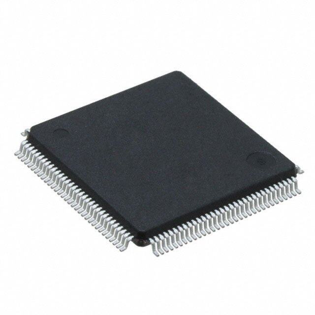
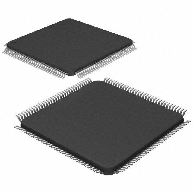
| 描述 | IC PCI-EXPRESS BRIDGE 128HTQFPPCI接口IC x1 PCI Exp to PCI Bus Trans Bridge |
| DevelopmentKit | XIO2001EVM |
| 产品分类 | |
| 品牌 | Texas Instruments |
| 产品手册 | |
| 产品图片 |
|
| rohs | 符合RoHS无铅 / 符合限制有害物质指令(RoHS)规范要求 |
| 产品系列 | 接口 IC,PCI接口IC,Texas Instruments XIO2001PNP- |
| NumberofLanes | 1 Lane |
| 数据手册 | 点击此处下载产品Datasheethttp://www.ti.com/lit/pdf/slyb174 |
| 产品型号 | XIO2001PNP |
| PCN组件/产地 | |
| 产品种类 | PCI接口IC |
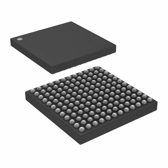
| 供应商器件封装 | 128-HTQFP(14x14) |
| 其它名称 | 296-32787 |
| 包装 | 托盘 |
| 商标 | Texas Instruments |
| 安装类型 | 表面贴装 |
| 安装风格 | SMD/SMT |
| 封装 | Tray |
| 封装/外壳 | 128-TQFP 裸露焊盘 |
| 封装/箱体 | HTQFP-128 |
| 工作电源电压 | 3.3 V, 1.5 V |
| 工厂包装数量 | 90 |
| 应用 | PCI Express 至 PCI 转换桥 |
| 接口 | PCI Express |
| 数据总线宽度 | 32 bit |
| 最大工作温度 | + 70 C |
| 最大数据速率 | 2 Gbps |
| 最大时钟频率 | 66 MHz |
| 最小工作温度 | 0 C |
| 标准包装 | 90 |
| 电压-电源 | 1.35 V ~ 1.65 V,3 V ~ 3.6 V |
| 类型 | Bridge - PCIe to PCI |
| 系列 | XIO2001 |
| 通道数 | 1 Lane |


- 商务部:美国ITC正式对集成电路等产品启动337调查
- 曝三星4nm工艺存在良率问题 高通将骁龙8 Gen1或转产台积电
- 太阳诱电将投资9.5亿元在常州建新厂生产MLCC 预计2023年完工
- 英特尔发布欧洲新工厂建设计划 深化IDM 2.0 战略
- 台积电先进制程称霸业界 有大客户加持明年业绩稳了
- 达到5530亿美元!SIA预计今年全球半导体销售额将创下新高
- 英特尔拟将自动驾驶子公司Mobileye上市 估值或超500亿美元
- 三星加码芯片和SET,合并消费电子和移动部门,撤换高东真等 CEO
- 三星电子宣布重大人事变动 还合并消费电子和移动部门
- 海关总署:前11个月进口集成电路产品价值2.52万亿元 增长14.8%


PDF Datasheet 数据手册内容提取
Product Sample & Technical Tools & Support & Folder Buy Documents Software Community XIO2001 SCPS212I–MAY2009–REVISEDJANUARY2016 XIO2001 PCI Express to PCI Bus Translation Bridge 1 Features • Five3.3-V,Multifunction,General-PurposeI/O Terminals • Full×1PCIExpress™Throughput 1 • Memory-MappedEEPROMSerial-BusController • FullyCompliantWith PCIExpresstoPCI/PCI-X SupportingPCIExpressPowerBudget/Limit BridgeSpecification,Revision1.0 ExtensionsforAdd-InCards • FullyCompliantWith PCIExpressBase • CompactFootprint,Lead-Free144-Ball,ZAJ Specification,Revision2.0 MicroStar™BGA,Lead-Free169-BallZGU • FullyCompliantWith PCILocalBusSpecification, MicroStarBGA,andPowerPad™HTQFP128-Pin Revision2.3 PNPPackage • PCIExpressAdvancedErrorReportingCapability IncludingECRCSupport 2 Applications • SupportforD1,D2,D3 ,andD3 hot cold • ConsumerApplications: • Active-StateLinkPowerManagementSaves – PC PowerWhenPacketActivityonthePCIExpress – Notebooks LinkisIdle,UsingBothL0sandL1States – PCIeAdd-InCards • WakeEventandBeaconSupport – Multi-FunctionPrinters • ErrorForwardingIncludingPCIExpressData PoisoningandPCIBusParityErrors – NetworkRoutersandSwitches • Uses100-MHzDifferentialPCIExpressCommon • IndustrialApplications ReferenceClockor125-MHzSingle-Ended, – IndustrialPCs ReferenceClock – VideoSurveillanceSystems • OptionalSpreadSpectrumReferenceClockis Supported 3 Description • RobustPipelineArchitecturetoMinimize The XIO2001 is a single-function PCI Express to PCI TransactionLatency translation bridge that is fully compliant to the PCI Express to PCI/PCI-X Bridge Specification, Revision • FullPCILocalBus66-MHz/32-BitThroughput 1.0. For downstream traffic, the bridge simultaneously • SupportforSixSubordinatePCIBusMasterswith supports up to eight posted and four non-posted InternalConfigurable,2-LevelPrioritization transactions. For upstream traffic, up to six posted Scheme and four non-posted transactions are simultaneously • InternalPCIArbiterSupportingUpto6External supported. PCIMasters The PCI Express interface is fully compliant to the • AdvancedPCIExpressMessageSignaled PCIExpressBaseSpecification,Revision2.0. InterruptGenerationforSerialIRQInterrupts The PCI Express interface supports a ×1 link • ExternalPCIBusArbiterOption operating at full 250 MB/s packet throughput in each • PCIBus LOCKSupport direction simultaneously. Also, the bridge supports the advanced error reporting including extended CRC • JTAG/BSforProductionTest (ECRC) as defined in the PCI Express Base • PCI-Express CLKREQ Support Specification. Supplemental firmware or software is • ClockRunandPowerOverrideSupport requiredtofullyusebothofthesefeatures. • SixBufferedPCIClockOutputs(25MHz,33MHz, DeviceInformation(1) 50MHz,or66MHz) PARTNUMBER PACKAGE BODYSIZE(NOM) • PCIBusInterface3.3-Vand5.0-V(25MHzor 33MHzonlyat5.0V)ToleranceOptions HTQFP(128) 14.00mm×14.00mm NFBGA(144) 7.00mm×7.00mm • IntegratedAUXPowerSwitchDrainsV Power XIO2001 AUX OnlyWhenMainPowerIsOff BGAMICROSTAR 12.00mm×12.00mm (169) (1) For all available packages, see the orderable addendum at theendofthedatasheet. 1 An IMPORTANT NOTICE at the end of this data sheet addresses availability, warranty, changes, use in safety-critical applications, intellectualpropertymattersandotherimportantdisclaimers.PRODUCTIONDATA.
XIO2001 SCPS212I–MAY2009–REVISEDJANUARY2016 www.ti.com TypicalDiagram 2 SubmitDocumentationFeedback Copyright©2009–2016,TexasInstrumentsIncorporated ProductFolderLinks:XIO2001
XIO2001 www.ti.com SCPS212I–MAY2009–REVISEDJANUARY2016 Table of Contents 1 Features.................................................................. 1 7 ParameterMeasurementInformation................24 2 Applications........................................................... 1 8 DetailedDescription............................................ 26 3 Description............................................................. 1 8.1 Overview.................................................................26 4 RevisionHistory..................................................... 3 8.2 FunctionalBlockDiagram.......................................26 5 PinConfigurationandFunctions......................... 5 8.3 FeatureDescription.................................................26 5.1 PinAssignments.......................................................5 8.4 RegisterMaps ........................................................42 5.2 PinDescriptions........................................................8 8.5 PCIExpressExtendedConfigurationSpace..........91 8.6 Memory-MappedTIProprietaryRegisterSpace..102 6 Specifications....................................................... 15 9 Application,Implementation,andLayout....... 114 6.1 AbsoluteMaximumRatings....................................15 6.2 HandlingRatings.....................................................15 9.1 ApplicationInformation..........................................114 6.3 RecommendedOperatingConditions.....................15 9.2 TypicalApplication................................................114 6.4 ThermalInformation ...............................................16 9.3 Layout................................................................... 124 6.5 NominalPowerConsumption.................................17 9.4 PowerSupplyRecommendations.........................127 6.6 PCIExpressDifferentialTransmitterOutput 10 DeviceandDocumentationSupport............... 130 Ranges.....................................................................17 10.1 DocumentsConventions.....................................130 6.7 PCIExpressDifferentialReceiverInputRanges....18 10.2 DocumentationSupport......................................131 6.8 PCIExpressDifferentialReferenceClockInput 10.3 Trademarks.........................................................131 Ranges.................................................................... 19 10.4 ElectrostaticDischargeCaution..........................131 6.9 PCIBusElectricalCharacteristics .........................20 10.5 Glossary..............................................................131 6.10 3.3-VI/OElectricalCharacteristics ......................20 11 Mechanical,Packaging,andOrderable 6.11 PCIBusTimingRequirements.............................21 Information......................................................... 131 6.12 Power-Up/-DownSequencing...............................21 4 Revision History REVISION REVISION REVISIONCOMMENTS DATE NUMBER 5/2009 – Initialrelease 5/2009 A Correctedtypos 9/2009 B AddedPNPPackageandESDRatings 10/2009 C Removedterminalassignmenttablesforallpackages 1/2010 D CorrectedPNPpinout,replacedOrderingInformationwithPackageOptionAddendum CorrectedViPCIExpressREFCLK(differential)parameters 11/2011 E CorrectedVRX-DIFFp-pparameters RemovedlabelN13onthesignalVDD_15fortheZAJpackage 5/2012 F AddedmissingPNPpinnumberstotheTable2-1andtotheTable2-2 ChangedexternalpartsforCLKRUN_ENtoincludepulldownresostor DeletedNotefromCLKRUIN_ENterminal'sdescription 5/2012 G ChangedexternalPartsforEXT_ARB_ENtoincludepulldownresistor DeletedNotefromEXT_ARB_ENterminal'sdescription AddedPinConfigurationandFunctionssection,HandlingRatingtable,FeatureDescriptionsection, DeviceFunctionalModes,ApplicationandImplementationsection,PowerSupplyRecommendations section,Layoutsection,DeviceandDocumentationSupportsection,andMechanical,Packaging,and 8/2014 H OrderableInformationsection UpdatedPower-UpSequencesection IdentifiedVDD_15_PLLpins Copyright©2009–2016,TexasInstrumentsIncorporated SubmitDocumentationFeedback 3 ProductFolderLinks:XIO2001
XIO2001 SCPS212I–MAY2009–REVISEDJANUARY2016 www.ti.com Revision History (continued) REVISION REVISION REVISIONCOMMENTS DATE NUMBER ChangedpinF10From:VDD_15To:VDD_15_PLLintheZGUpackage ChangedpinF11From:VDD_15To:VDD_15_PLLintheZAJpackage Changedpin84From:VDDA_15To:VDD_15_PLLinthePNPpackage ChangedthepinnamefromVDD_15_PULLtoVDD_15_PLLinthePinFunctionstable. 9/2014 I ChangedPCIRdescriptioninthePinFunctionstableFrom:"ConnectthisterminalstothesecondaryPCI bus..."To:"ConnecteachoneoftheseterminalstothesecondaryPCIbus.." DeletedtextfromtheLOCKpindescriptioninthePinFunctionstable:"whenbit12(LOCK_EN)issetin thegeneralcontrolregister(seeGeneralControlRegister)." 4 SubmitDocumentationFeedback Copyright©2009–2016,TexasInstrumentsIncorporated ProductFolderLinks:XIO2001
XIO2001 www.ti.com SCPS212I–MAY2009–REVISEDJANUARY2016 5 Pin Configuration and Functions 5.1 Pin Assignments TheXIO2001isavailableineithera169-ballZGUMicroStarBGAora144−ballZAJMicroStarBGApackage. Figure1 showsapindiagramoftheZGUpackage. Figure2 showsapindiagramoftheZAJpackage. Figure3 showsapindiagramofthePNPpackage. 1 2 3 4 5 6 7 8 9 10 11 12 13 N C/BE[3] AD25 AD27 AD30 AD31 INTB PRST SERIRQ GPIO0// GPIO2 GPIO3//SDA JTAG_TDI GRST NN CLKRUN M AD20 AD22 AD24 AD26 AD28 INTA INTC LOCK GPIO1// GPIO4// JTAG_TDO JTAG_TCK WAKE MM PWR_OVRD SCL L AD18 AD19 AD21 AD23 AD29 M66EN INTD VDD_33 JTAG_ JTAG_TMS VSS PME VDD_15_ LL TRST# COMB K AD16 AD17 PCIR VSS VSS VSS VDD_15 VSS VDD_33 VSSA VDD_33_ REF0_PCIE REF1_PCIE KK COMB_IO J IRDY FRAME C/BE[2] VDD_33 VSS VSS VSS VSS VSS VSS VDD_33_ VDD_33 VDD_33_ JJ AUX COMB H TRDY DEVSEL VDD_33 VSS VSS VSS VSS VSS VSS VDD_15 PERST VSSA VDDA_15 HH G STOP PERR SERR# VDD_15 VSS VSS VSS VSS VSS VDD_15 VSSA TXN TXP GG FF FF PAR C/BE[1] CLK VSS VSS VSS VSS VSS VSS VDD_15_PLL VSS VSS VDDA_15 E AD15 AD14 AD13 VDD_33 VSS VSS VSS VSS VSS VSSA VSSA RXN RXP EE D AD12 AD11 AD8 VSS VDD_33 VSS VDD_15 VSS VDD_33 VSS CLKREQ VREG_PD33 VDDA_33 DD C AD10 AD9 AD7 AD5 AD0 GNT1 VDD_33 REQ3 REQ4 EXT_ARB_EN VSSA REFCLK– REFCLK+ CC B C/BE[0] AD6 AD3 AD2 CLKOUT0 CLKOUT1 CLKOUT3 GNT2 GNT3 GNT5 CLKOUT6 PCLK66_SEL REFCLK125 BB _SEL A PCIR AD4 AD1 REQ0 GNT0 REQ1 CLKOUT2 REQ2 CLKOUT4 CLKOUT5 GNT4 REQ5 CLKRUN_EN AA 1 2 3 4 5 6 7 8 9 10 11 12 13 Figure1. XIO2001ZGUMicroStarBGAPackage(BottomView) Copyright©2009–2016,TexasInstrumentsIncorporated SubmitDocumentationFeedback 5 ProductFolderLinks:XIO2001
XIO2001 SCPS212I–MAY2009–REVISEDJANUARY2016 www.ti.com Pin Assignments (continued) 1 2 3 4 5 6 7 8 9 10 11 12 13 N AD21 AD24 AD27 AD28 AD31 INTA INTD LOCK GPIO0// GPIO2 JTAG_TDO JTAG_TCK VDD_15_ NN CLKRUN COMB M AD18 AD22 C/BE[3] AD25 AD29 M66EN INTC SERIRQ GPIO1// GPIO4_ GRST PME REF0_PCIE MM PWR_OVRD SCL L AD16 AD20 AD23 AD26 AD30 INTB PRST GPIO3//SDA JTAG_ JTAG_TDI JTAG_TMS WAKE REF1_PCIE LL TRST K C/BE[2] AD19 AD17 VDD_33_ VDD_33_ VDD_15 KK COMB_IO COMB J FRAME TRDY PCIR VSS VSS VDD_15 VDD_15 VSS VDD_33 VDD_33_ VSSA JJ AUX H STOP DEVSEL IRDY VSS VDD_33 VDD_33 VDD_15 VSS PERST VDDA_15 TXP HH G PAR SERR PERR VSS VDD_33 VDD_33 VDD_15 VSSA VDD_15 VSSA TXN GG FF CLK AD15 C/BE[1] VSS VDD_33 VDD_33 VDD_33 VSS VDD_15_PLL VSS VSSA FF E AD13 AD12 AD14 VDD_33 VSS VSS VSS VSS VREG_PD33 VDDA_15 RXP EE D AD11 AD9 PCIR CLKREQ VSSA RXN DD C AD10 C/BE[0] AD5 AD2 AD1 REQ1 REQ2 REQ3 REQ5 CLKOUT6 CLKRUN_EN VDDA_33 REFCLK+ CC B AD8 AD6 AD0 CLKOUT0 CLKOUT1 CLKOUT2 GNT2 GNT3 GNT4 GNT5 VSSA REFCLK- BB A AD7 AD4 AD3 REQ0 GNT0 GNT1 CLKOUT3 CLKOUT4 REQ4 CLKOUT5 PCLK66_ EXT_ARB_ REFCLK125 AA SEL EN _SEL 1 2 3 4 5 6 7 8 9 10 11 12 13 Figure2. XIO2001ZAJMicroStarBGAPackage(BottomView) 6 SubmitDocumentationFeedback Copyright©2009–2016,TexasInstrumentsIncorporated ProductFolderLinks:XIO2001
XIO2001 www.ti.com SCPS212I–MAY2009–REVISEDJANUARY2016 Pin Assignments (continued) ELEN 33 UT0 UT1 UT215UT333 UT4 UT5 33UT666_SARB_ 65D_43210KOQ0T0KOQ1T1KOD_KOD_Q2T2Q3KOT3Q4KOT4Q5T5D_KOLKT_ DDDDDDDDLENLENLDLDENELNELNENDLCX AAVAAAAACRGCRGCVCVRGRCGRCGRGVCPE 128127126125124123122121120119118117116115114113112111110109108107106105104103102101100999897 AD7 1 96 CLKRUN_EN PCIR 2 95 REFCLK125_SEL C/BE[0] 3 94 REFCLK– AD8 4 93 REFCLK+ AD9 5 92 VDDA_33 AD10 6 91 CLKREQ VDD_33 7 90 VREG_PD33 AD11 8 89 VSSA AD12 9 88 RXN AD13 10 87 RXP AD14 11 86 VSSA AD15 12 85 VDDA_15 CLK 13 84 VDD_15_PLL C/BE[1] 14 83 VDDA_15 PAR 15 82 VSSA SERR 16 81 TXN PERR 17 80 TXP STOP 18 79 VSSA VDD_33 19 78 VDDA_15 DEVSEL 20 77 PERST VDD_15 21 76 VDDA_15 TRDY 22 75 VDD_33_COMB IRDY 23 74 VDDA_33 FRAME 24 73 VDD_33_AUX C/BE[2] 25 72 REF1_PCIE AD16 26 71 REF0_PCIE PCIR 27 70 VDD_33_COM_IO AD17 28 69 VDD_15_COMB AD18 29 68 WAKE AD19 30 67 PME AD20 31 66 GRST AD21 32 65 JTAG_TCK 34567890123456789012345678901234 33333334444444444555555555566666 VDD_33AD22AD23C/BE[3]AD24AD25AD26AD27AD28AD29AD30AD31M66ENVDD_33INTAINTBINTCINTDPRSTSERIRQVDD_15LOCKPIO0 //CLKRUN1 // PWR_OVERGPIO2GPIO3 // SDAGPIO4 // SCLJTAG_TRSTJTAG_TDOVDD_33JTAG_TDIJTAG_TMS GO PI G Figure3. XIO2001PNP PowerPAD™HTQFPPackage(TopView) Copyright©2009–2016,TexasInstrumentsIncorporated SubmitDocumentationFeedback 7 ProductFolderLinks:XIO2001
XIO2001 SCPS212I–MAY2009–REVISEDJANUARY2016 www.ti.com 5.2 Pin Descriptions Thefollowinglistdescribesthedifferentinput/outputcelltypesthatappearinthepinfunctiontables: • HSDIFFIN=Highspeeddifferentialinput • HSDIFFOUT=Highspeeddifferentialoutput • PCIBUS=PCIbustri-statebidirectionalbufferwith3.3-Vor5.0-Vclamprail. • LVCMOS=3.3-VlowvoltageCMOSinputoroutputwith3.3-Vclamprail • BIAS=Input/outputterminalsthatgenerateabiasvoltagetodetermineadriver'soperatingcurrent • Feed through = These terminals connect directly to macros within the part and not through an input or output cell. • PWR=Powerterminal • GND=Groundterminal PinFunctions ZGU ZAJ PNP I/O EXTERNAL SIGNAL BALL BALL PIN DESCRIPTION TYPE PARTS NO. NO. NO. POWERSUPPLY PCIR A01, D03,J03 2,27 I/O Resistor PCIRail.5.0-Vor3.3-VPCIbusclampvoltagetosetmaximum K03 I/OvoltagetoleranceofthesecondaryPCIbussignals.Connect eachoneoftheseterminalstothesecondaryPCIbusI/Oclamp railthrougha1kΩresistor. V G04, J08, 21,53, PWR Bypass 1.5-Vdigitalcorepowerterminals DD_15 K07, H08, 113 capacitors D07, J07, H10, G08, G10 K13,G11 V F10 F11 84 PWR Pifilter 1.5-VpowerterminalforinternalPLL.Thisterminalmustbe DD_15_PLL isolatedfromanaloganddigitalpower. V F13, E12,H12 76,78, PWR Pifilter 1.5-Vanalogpowerterminal DDA_15 H13 83,85 V E04, E05, 7,19, PWR Bypass 3.3-VdigitalI/Opowerterminal DD_33 H03, G06, 33,46, capacitors J04, H07, 62,100, L08, G07, 111, K09, H06, 126 D09, F08, C07, F07, D05, F06,J11 J12 V J11 J12 73 PWR Bypass 3.3-VauxiliarypowerterminalNote:Thisterminalisconnected DD_33_AUX capacitors toV throughapulldownresistorifnoauxiliarysupplyis SS present. V D13 C12 74,92 PWR Pifilter 3.3-Vanalogpowerterminal DDA_33 GROUND V D04, E06, GND Digital SS F04, F05, ground H04, G05, terminals K04, H05, K05, J05,J06, K06, J09, K08, H09, L11, E09, J10, E08, D10, E07,F12 D08, ,F09 D06, F11, F12 8 SubmitDocumentationFeedback Copyright©2009–2016,TexasInstrumentsIncorporated ProductFolderLinks:XIO2001
XIO2001 www.ti.com SCPS212I–MAY2009–REVISEDJANUARY2016 Pin Descriptions (continued) PinFunctions(continued) ZGU ZAJ PNP I/O EXTERNAL SIGNAL BALL BALL PIN DESCRIPTION TYPE PARTS NO. NO. NO. V E05, GND Ground SS E06, terminalsfor E07, thermally- E08, enhanced E09, package F05, F06, F07, F08, F09, G05, G06, G07, G08, G09, H05, H06, H07, H08, H09, J05, J06, J07, J08, J09 V K10, G09, 79,82, GND Analog SSA C11, B12,J13, 86,89 ground H12, G12, terminal G11, F13,D12 E11, E10 COMBINEDPOWEROUTPUT V L13 N13 69 Internally-combined1.5-VmainandV poweroutputfor DD_15_COMB AUX externalbypasscapacitorfiltering.Suppliesallinternal1.5-V Feed Bypass circuitrypoweredbyV . through capacitors AUX Caution: Do not use this terminal to supply external power to otherdevices. V J13 K12 75 Internally-combined3.3-VmainandV poweroutputfor DD_33_COMB AUX externalbypasscapacitorfiltering.Suppliesallinternal3.3-V Feed Bypass circuitrypoweredbyV . through capacitors AUX Caution: Do not use this terminal to supply external power to otherdevices. V K11 K11 70 Internally-combined3.3-VmainandV poweroutputfor DD_33_COMBIO AUX externalbypasscapacitorfiltering.Suppliesallinternal3.3-V Feed Bypass input/outputcircuitrypoweredbyV . through capacitors AUX Caution: Do not use this terminal to supply external power to otherdevices. Copyright©2009–2016,TexasInstrumentsIncorporated SubmitDocumentationFeedback 9 ProductFolderLinks:XIO2001
XIO2001 SCPS212I–MAY2009–REVISEDJANUARY2016 www.ti.com PinFunctions ZGU ZAJ PNP I/O CELL CLAMP EXTERNAL SIGNAL BALL DESCRIPTION BALLNO. PINNO. TYPE TYPE RAIL PARTS NO. PCIEXPRESS CLKREQ D11 D11 91 0 LV VDD_33_ Clockrequest.Whenassertedlow,requests CMOS COMBIO upstreamdevicestartclockincaseswhereclock mayberemovedinL1. – Note: Since CLKREQ is an open-drain outputbuffer, a system sidepullupresistor isrequired. PERST H11 H11 77 I LV VDD_33_ PCIExpressresetinput.ThePERSTsignal CMOS COMBIO identifieswhenthesystempowerisstableand – generatesaninternalpoweronreset. Note: The PERST input buffer has hysteresis. REFCLK125_SEL B13 A13 95 I LV VDD_33 Referenceclockselect.Thisterminalselectsthe CMOS referenceclockinput. Pullupor 0=100-MHzdifferentialcommonreference pulldown clockused. resistor 1=125-MHzsingle-ended,referenceclock used. REFCLK+ C13 C13 93 DI HSDIFF VDD_33 Referenceclock.REFCLK+andREFCLK– IN comprisethedifferentialinputpairforthe100- – MHzsystemreferenceclock.Forasingle-ended, 125-MHzsystemreferenceclock,usethe REFCLK+input. REFCLK– C12 B13 94 DI HSDIFF VDD_33 Capacitor Referenceclock.REFCLK+andREFCLK– IN comprisethedifferentialinputpairforthe100- forVSSfor MHzsystemreferenceclock.Forasingle-ended, single- 125-MHzsystemreferenceclock,attacha endednode capacitorfromREFCLK–toVSS. REF0_PCIE K12 M13 71 I/O BIAS – Externalreferenceresistor+and–terminalsfor REF1_PCIE K13 L13 72 settingTXdrivercurrent.Anexternalresistance of14,532-ΩisconnectedbetweenREF0_PCIE External andREF1_PCIEterminals.Toeliminatetheneed resistor foracustomresistor,twoseriesresistorsare recommended:a14.3-kΩ,1%resistoranda232- Ω,1%resistor. RXP E13 E13 87 DI HSDIFF VSS High-speedreceivepair.RXPandRXNcomprise RXN E12 D13 88 IN – thedifferentialreceivepairforthesinglePCI Expresslanesupported. TXP G13 H13 80 DO HSDIFF VDD_15 Series High-speedtransmitpair.TXPandTXNcomprise TXN G12 G13 81 OUT thedifferentialtransmitpairforthesinglePCI capacitor Expresslanesupported. WAKE M13 L12 68 O LV VDD_33_ Wakeisanactivelowsignalthatisdrivenlowto CMOS COMBIO reactivatethePCIExpresslinkhierarchy’smain powerrailsandreferenceclocks. – Note:SinceWAKEisanopen-drainoutput buffer, a system side pullup resistor is required. 10 SubmitDocumentationFeedback Copyright©2009–2016,TexasInstrumentsIncorporated ProductFolderLinks:XIO2001
XIO2001 www.ti.com SCPS212I–MAY2009–REVISEDJANUARY2016 PinFunctions(continued) ZGU ZAJ PNP I/O CELL CLAMP EXTERNAL SIGNAL BALL DESCRIPTION BALLNO. PINNO. TYPE TYPE RAIL PARTS NO. PCISYSTEM AD31 N05 N05 44 I/O PCIBus PCIR PCIaddressdatalines AD30 N04 L05 43 AD29 L05 M05 42 AD28 M05 N04 41 AD27 N03 N03 40 AD26 M04 L04 39 AD25 N02 M04 38 AD24 M03 N02 37 AD23 L04 L03 35 AD22 M02 M02 34 AD21 L03 N01 32 AD20 M01 L02 31 AD19 L02 K02 30 AD18 L01 M01 29 AD17 K02 K03 28 AD16 K01 L01 26 – AD15 E01 F02 12 AD14 E02 E03 11 AD13 E03 E01 10 AD12 D01 E02 9 AD11 D02 D01 8 AD10 C01 C01 6 AD9 C02 D02 5 AD8 D03 B01 4 AD7 C03 A01 1 AD6 B02 B03 128 AD5 C04 C03 127 AD4 A02 A02 125 AD3 B03 A03 124 AD2 B04 C04 123 AD1 A03 C05 122 AD0 C05 B04 121 C/BE[3] N01 M03 36 I/O PCIBus PCIR PCIcommandbyteenables C/BE[2] J03 K01 25 – C/BE[1] F02 F03 14 C/BE[0] B01 C02 3 CLK F03 F01 13 I PCIBus PCIR PCIclockinput.ThisistheclockinputtothePCI – buscore. CLKOUT0 B05 B05 120 O PCIBus PCIR PCIclockoutputs.Theseclockoutputsareused CLKOUT1 B06 B06 117 toclockthePCIbus.IfthebridgePCIbusclock CLKOUT2 A07 B07 114 outputsareused,thenCLKOUT6mustbe CLKOUT3 B07 A07 112 – connectedtotheCLKinput. CLKOUT4 A09 A08 107 CLKOUT5 A10 A10 104 CLKOUT6 B11 C10 99 DEVSEL H02 H02 20 I/O PCIBus PCIR Pullup PCIdeviceselect resistorper PCIspec FRAME J02 J01 24 I/O PCIBus PCIR Pullup PCIframe resistorper PCIspec GNT5 B10 B11 101 O PCIBus PCIR PCIgrantoutputs.Thesesignalsareusedfor GNT4 A11 B10 103 arbitrationwhenthePCIbusisthesecondary GNT3 B09 B09 106 busandanexternalarbiterisnotused.GNT0is – GNT2 B08 B08 109 usedastheREQforthebridgewhenanexternal GNT1 C06 A06 115 arbiterisused. GNT0 A05 A05 118 INTA M06 N06 47 I PCIBus PCIR PCIinterruptsA–D.Thesesignalsareinterrupt Pullup INTB N06 L06 48 inputstothebridgeonthesecondaryPCIbus. resistorper INTC M07 M07 49 PCIspec INTD L07 N07 50 IRDY J01 H03 23 I/O PCIBus PCIR Pullup PCIinitiatorready resistorper PCIspec LOCK M08 N08 54 I/O PCIBus PCIR ThisterminalfunctionsasPCILOCK Pullup Note: In lock mode, an external pullup resistorper PCIspec resistor is required to prevent the LOCK signalfromfloating. Copyright©2009–2016,TexasInstrumentsIncorporated SubmitDocumentationFeedback 11 ProductFolderLinks:XIO2001
XIO2001 SCPS212I–MAY2009–REVISEDJANUARY2016 www.ti.com PinFunctions(continued) ZGU ZAJ PNP I/O CELL CLAMP EXTERNAL SIGNAL BALL DESCRIPTION BALLNO. PINNO. TYPE TYPE RAIL PARTS NO. M66EN L06 M06 45 I PCIBus PCIR 66-MHzmodeenable 0 = Secondary PCI bus and clock outputs Pullup operate at 33 MHz. If PCLK66_SEL is low resistorper thenthefrequencywillbe25MHz. PCIspec 1 = Secondary PCI bus and clock outputs operate at 66 MHz. If PCLK66_SEL is low thenthefrequencywillbe50MHz. PAR F01 G01 15 I/O PCIBus PCIR – PCIbusparity PERR G02 G03 17 I/O PCIBus PCIR Pullup PCIparityerror resistorper PCIspec PME L12 M12 67 I LV VDD_33_ PullupresistorperPCIspecPCIpower CMOS COMBIO Pullup managementevent.Thisterminalmaybeusedto resistorper detectPMEeventsfromaPCIdeviceonthe PCIspec secondarybus. Note:ThePMEinputbufferhashysteresis. REQ5 A12 C09 102 I PCIBus PCIR PCIrequestinputs.Thesesignalsareusedfor REQ4 C09 A09 105 Ifunused,a arbitrationonthesecondaryPCIbuswhenan REQ3 C08 C08 108 weakpullup externalarbiterisnotused.REQ0isusedasthe REQ2 A08 C07 110 resistorper GNTforthebridgewhenanexternalarbiteris REQ1 A06 C06 116 PCIspec used. REQ0 A04 A04 119 PRST N07 L07 51 O PCIBus PCIR PCIreset.Thisterminalisanoutputtothe – secondaryPCIbus. SERR G03 G02 16 I/O PCIBus PCIR Pullup PCIsystemerror resistorper PCIspec STOP G01 H01 18 I/O PCIBus PCIR Pullup PCIstop resistorper PCIspec TRDY H01 J02 22 I/O PCIBus PCIR Pullup PCItargetready resistorper PCIspec JTAG JTAG_TCK M12 N12 65 I LV VDD_33 JTAGtestclockinput.Thissignalprovidesthe CMOS clockfortheinternalTAPcontroller. Note: This terminal has an internal active Optional pullup resistor. The pullup is active at all pullup times. resistor Note: This terminal should be tied to ground or pulled low if JTAG is not required. JTAG_TDI N12 L10 63 I LV VDD_33 JTAGtestdatainput.Serialtestinstructionsand CMOS dataarereceivedonthisterminal. Optional Note: This terminal has an internal active pullup pullup resistor. The pullup is active at all resistor times. Note: This terminal can be left unconnectedifJTAGisnotrequired. JTAG_TDO M11 N11 61 O LV VDD_33 JTAGtestdataoutput.Thisterminaltheserial CMOS outputfortestinstructionsanddata. – Note: This terminal can be left unconnectedifJTAGisnotrequired. JTAG_TMS L10 L11 64 I LV VDD_33 JTAGtestmodeselect.Thesignalreceivedat CMOS JTAG_TMSisdecodedbytheinternalTAP controllertocontroltestoperations. Optional Note: This terminal has an internal active pullup pullup resistor. The pullup is active at all resistor times. Note: This terminal can be left unconnectedifJTAGisnotrequired. 12 SubmitDocumentationFeedback Copyright©2009–2016,TexasInstrumentsIncorporated ProductFolderLinks:XIO2001
XIO2001 www.ti.com SCPS212I–MAY2009–REVISEDJANUARY2016 PinFunctions(continued) ZGU ZAJ PNP I/O CELL CLAMP EXTERNAL SIGNAL BALL DESCRIPTION BALLNO. PINNO. TYPE TYPE RAIL PARTS NO. JTAG_TRST L09 L09 60 I LV VDD_33 JTAGtestreset.ThisterminalprovidesOptional CMOS forasynchronousinitializationoftheTAP controller. Optional Note: This terminal has an internal active pullup pullup resistor. The pullup is active at all resistor times. Note: This terminal should be tied to ground or pulled low if JTAG is not required. MiscellaneousPins ZGU ZAJ PNP I/O CELL CLAMP EXTERNAL SIGNAL BALL BALL PIN DESCRIPTION TYPE TYPE RAIL PARTS NO. NO. NO. CLKRUN_ A13 C11 96 I LV V Optional Clockrunenable DD_33 EN CMOS pullup/ 0=Clockrunsupportdisabled pulldown resistor 1=Clockrunsupportenabled EXT_ARB_EN C10 A12 97 I LV VDD_33 Optional Externalarbiterenable CMOS pullup/ pulldown 0=Internalarbiterenabled resistor 1=Externalarbiterenabled GPIO0// N09 N09 55 I/O LV V DD_33 General-purpose I/O 0/clock run. This CLKRUN CMOS terminal functions as a GPIO controlled by bit 0 (GPIO0_DIR) in the GPIO control register (see GPIO Control Register) or the clock run terminal. This terminalisusedasclockruninputwhen Optionalpullup thebridgeisplacedinclockrunmode. resistor Note: In clock run mode, an external pullupresistor is requiredtopreventthe CLKRUNsignalfromfloating. Note: This terminal has an internal active pullup resistor. The pullup is only active when reset is asserted or when theGPIOisconfiguredasaninput. GPIO1//PWR_ M09 M09 56 I/O LV V DD_33 General-purpose I/O 1/power override. OVRD CMOS This terminal functions as a GPIO controlled by bit 1 (GPIO1_DIR) in the GPIOcontrolregister(seeGPIOControl Register) or the power override output terminal. GPIO1 becomes PWR_OVRD – whenbits22:20(POWER_OVRD)inthe general control register are set to 001b or011b(seeGeneralControlRegister). Note: This terminal has an internal active pullup resistor. The pullup is only active when reset is asserted or when theGPIOisconfiguredasaninput. GPIO2 N10 N10 57 I/O LV V DD_33 General-purpose I/O 2. This terminal CMOS functions as a GPIO controlled by bit 2 (GPIO2_DIR) in the GPIO control register(seeGPIOControlRegister). – Note: This terminal has an internal active pullup resistor. The pullup is only active when reset is asserted or when theGPIOisconfiguredasaninput. Copyright©2009–2016,TexasInstrumentsIncorporated SubmitDocumentationFeedback 13 ProductFolderLinks:XIO2001
XIO2001 SCPS212I–MAY2009–REVISEDJANUARY2016 www.ti.com MiscellaneousPins(continued) ZGU ZAJ PNP I/O CELL CLAMP EXTERNAL SIGNAL BALL BALL PIN DESCRIPTION TYPE TYPE RAIL PARTS NO. NO. NO. GPIO3//SDA N11 L08 58 I/O LV V DD_33 GPIO3 or serial-bus data. This terminal CMOS functions as serial-bus data if a pullup resistorisdetectedonSCLorwhenthe SBDETECT bit is set in the Serial Bus ControlandStatusRegister(seeSerial- Optionalpullup Bus Control and Status Register). If no resistor pullup is detected then this terminal functionsasGPIO3. Note: In serial-bus mode, an external pullupresistor is requiredtopreventthe SDAsignalfromfloating. GPIO4//SCL M10 M10 59 I/O LV V DD_33 GPIO4orserial-busclock.Thisterminal CMOS functions as serial-bus clock if a pullup resistorisdetectedonSCLorwhenthe SBDETECT bit is set in the Serial Bus ControlandStatusRegister(seeSerial- Bus Control and Status Register). If no pullup is detected then this terminal Optionalpullup functionsasGPIO4. resistor Note: In serial-bus mode, an external pullupresistor is requiredtopreventthe SCLsignalfromfloating. Note: This terminal has an internal active pullup resistor. The pullup is only active when reset is asserted or when theGPIOisconfiguredasaninput. GRST N13 M11 66 I LV V DD_33 Global reset input. Asynchronously CMOS _COMBIO resetsalllogicindevice,includingsticky bits and power management state – machines. Note: The GRST input buffer has both hysteresis and an internal active pullup. Thepullupisactiveatalltimes. PCLK66_ B12 A11 98 I LV V DD_33 PCI clock select. This terminal SEL CMOS determines the default PCI clock frequency driven out the CLKOUTx terminals. Optional 0=50MHzPCIClock pulldown 1=66MHzPCIClock resistor Note: This terminal has an internal active pullup resistor. This pullup is activeatalltimes. Note: M66EN terminal also has an affectofPCIclockfrequency. SERIRQ N08 M08 52 I/O PCI PCIR Serial IRQ interface. This terminal Bus Pullupor functions as a serial IRQ interface if a pulldown pullup is detected when PERST is resistor deasserted. If a pulldown is detected, thentheserialIRQinterfaceisdisabled. VREG_ D12 E11 90 I LV V 3.3-Vvoltageregulatorpowerdown.This DD_33 PD33 CMOS Pulldown terminalshouldalwaysbetieddirectlyto _COMBIO resistor groundoranoptionalpulldownresistor canbeused. 14 SubmitDocumentationFeedback Copyright©2009–2016,TexasInstrumentsIncorporated ProductFolderLinks:XIO2001
XIO2001 www.ti.com SCPS212I–MAY2009–REVISEDJANUARY2016 6 Specifications 6.1 Absolute Maximum Ratings overoperatingtemperaturerange(unlessotherwisenoted)(1) MIN MAX UNIT V –0.5 3.6 V DD_33 Supplyvoltagerange V –0.5 1.65 V DD_15 PCI –0.5 PCIR+0.5 V PCIExpress(RX) –0.6 0.6 V V Inputvoltagerange PCIExpressREFCLK(single-ended) –0.5 V +0.5 V I DD_33 PCIExpressREFCLK(differential) –0.5 V +0.5 V DD_15 Miscellaneous3.3-VIO –0.5 V +0.5 V DD_33 PCI –0.5 V +0.5 V DD_33 V Outputvoltagerange PCIExpress(TX) –0.55 V +0. V O DD_15 Miscellaneous3.3-VIO –0.5 V +0.5 V DD_33 Inputclampcurrent,(V <0orV >VDD)(2) ±20 mA I I Outputclampcurrent,(V <0orV >VDD)(3) ±20 mA O O (1) StressesbeyondthoselistedunderAbsoluteMaximumRatingsmaycausepermanentdamagetothedevice.Thesearestressratings only,andfunctionaloperationofthedeviceattheseoranyotherconditionsbeyondthoseindicatedunderRecommendedOperating Conditionsisnotimplied.Exposuretoabsolute-maximum-ratedconditionsforextendedperiodsmayaffectdevicereliability. (2) Appliesforexternalinputandbidirectionalbuffers.V <0orV >V orV >PCIR. I I DD I (3) Appliesforexternalinputandbidirectionalbuffers.V <0orV >V orV >PCIR. O O DD O 6.2 Handling Ratings MIN MAX UNIT T Storagetemperaturerange –65 150 °C stg V (1) HumanbodymodelESDrating(R=1.5K,C=100pF) 2 kV ESD-HBM V (1) ChargeddevicemodelESDrating(200pF) 500 V ESD-CDM (1) Electrostaticdischarge(ESD)tomeasuredevicesensitivityandimmunitytodamagecausedbyassemblylineelectrostaticdischargesin tothedevice. 6.3 Recommended Operating Conditions OPERATION MIN NOM MAX UNIT V DD_15 Supplyvoltage 1.5V 1.35 1.5 1.65 V V DDA_15 V DD_33 V Supplyvoltage 3.3V 3 3.3 3.6 V DDA_33 V DDA_33_AUX 3.3V 3 3.3 3.6 PCIR PCIbusclampingrailvoltage(with1kΩresistor) V 5V 4.75 5 5.25 Copyright©2009–2016,TexasInstrumentsIncorporated SubmitDocumentationFeedback 15 ProductFolderLinks:XIO2001
XIO2001 SCPS212I–MAY2009–REVISEDJANUARY2016 www.ti.com 6.4 Thermal Information(1) PARAMETER TESTCONDITIONS MIN TYP MAX UNIT PNP Low-KJEDECtestboard,1s(singlesignallayer),noair 50.8 Junction-to-free-airthermal flow θ °C/W JA resistance High-KJEDECtestboard,2s2p(doublesignallayer, 24.9 doubleburiedpowerplane),noairflow θ Junction-to-casethermalresistance Cucoldplatemeasurementprocess 18.9 °C/W JC Junction-to-boardthermal θ EIA/JESD51-8 14.6 °C/W JB resistance ψ Junction-to-topofpackage EIA/JESD51-2 0.26 °C/W JT ψ Junction-to-board EIA/JESD51-6 7.93 °C/W JB Operatingambienttemperature XIO2001PNP 0 70 T °C A range XIO2001IPNP –40 85 XIO2001PNP 0 105 T Virtualjunctiontemperature °C J XIO2001IPNP –40 105 ZAJ Low-KJEDECtestboard,1s(singlesignallayer),noair 82 Junction-to-free-airthermal flow θ °C/W JA resistance High-KJEDECtestboard,2s2p(doublesignallayer, 58.8 doubleburiedpowerplane),noairflow θ Junction-to-casethermalresistance Cucoldplatemeasurementprocess 19 °C/W JC Junction-to-boardthermal θ EIA/JESD51-8 32 °C/W JB resistance ψ Junction-to-topofpackage EIA/JESD51-2 0.5 °C/W JT ψ Junction-to-board EIA/JESD51-6 30 °C/W JB Operatingambienttemperature XIO2001ZGU 0 70 T °C A range XIO2001IZGU –40 85 XIO2001ZGU 0 105 T Virtualjunctiontemperature °C J XIO2001IZGU –40 105 ZGU Low-KJEDECtestboard,1s(singlesignallayer),noair 85 Junction-to-free-airthermal flow θ °C/W JA resistance High-KJEDECtestboard,2s2p(doublesignallayer, 48.3 doubleburiedpowerplane),noairflow θ Junction-to-casethermalresistance Cucoldplatemeasurementprocess 8.5 °C/W JC Junction-to-boardthermal θ EIA/JESD51-8 25.4 °C/W JB resistance ψ Junction-to-topofpackage EIA/JESD51-2 0.5 °C/W JT ψ Junction-to-board EIA/JESD51-6 24 °C/W JB Operatingambienttemperature XIO2001ZGU 0 70 T °C A range XIO2001IZGU –40 85 XIO2001ZGU 0 105 T Virtualjunctiontemperature °C J XIO2001IZGU –40 105 (1) Formoredetails,refertoTIapplicationnoteICPackageThermalMetrics(SPRA953). 16 SubmitDocumentationFeedback Copyright©2009–2016,TexasInstrumentsIncorporated ProductFolderLinks:XIO2001
XIO2001 www.ti.com SCPS212I–MAY2009–REVISEDJANUARY2016 6.5 Nominal Power Consumption DEVICES POWERSTATE(1) VOLTS AMPERES WATTS 1.5 0.147 0.221 NodownstreamPCIdevices D0idle 3.3 0.062 0.205 TOTALS: 0.209 0.426 1.5 0.148 0.222 OnedownstreamPCIdevice D0idle 3.3 0.077 0.254 TOTALS: 0.225 0.476 1.5 0.157 0.236 OnedownstreamPCIdevice D0active 3.3 0.165 0.545 TOTALS: 0.322 0.780 1.65 0.168 0.277 Onedownstream(maxvoltage) D0active 3.6 0.188 0.677 TOTALS: 0.356 0.954 (1) D0idlepowerstate:DownstreamPCIdeviceisinPCIstateD0.Downstreamdevicedriverisloaded.Downstreamdeviceisnotactively transferringdata. D0activepowerstate:DownstreamPCIdeviceisinPCIstateD0.Downstreamdevicedriverisloaded.Downstreamdeviceisacitvely transferringdata(worstcasescenario). 6.6 PCI Express Differential Transmitter Output Ranges PARAMETER TERMINALS MIN NOM MAX UNIT COMMENTS UI(1) EachUIis400ps±300ppm.UIdoesnotaccountforSSC TXP,TXN 399.88 400 400.12 ps Unitinterval dictatedvariations. VDTifXfe-DrIeFnF-tPiaPlpeak-to-peakoutputvoltage TXP,TXN 0.8 1.2 V VTX-DIFF-PP=2*|VTXP–VTXN| VTX-DIFF-PP-LOW Low-powerdifferentialpeak-to-peakTX TXP,TXN 0.4 1.2 V VTX-DIFF-PP=2*|VTXP–VTXN| voltageswing VTXTX-dDeE--eRAmTpIOh-3a.5sdisBlevelratio TXP,TXN 3 4 dB TfohllioswisintghebirtastaioftoefrtahetraVnTsXi-tDioIFnF-dPPivoidfetdhebysethcoenVdTXa-nDdIFF-PPof thefirstbitafteratransition. TMTiXn-iEmYuEm(2)T(3X)(e4)yewidth TXP,TXN 0.75 UI DoesnotincludeSSCorRefCLKjitter.IncludesRjat10–12. TTX-EYE-MEDIAN-to-MAX-JITTER(2) Measureddifferentiallyatzerocrossingpointsafter Maximumtimebetweenthejittermedian TXP,TXN 0.125 UI applyingthe2.5GT/sclockrecoveryfunction. andmaximumdeviationfromthemedian TTX-RISE-FALL(2) TXP,TXN 0.125 UI Measureddifferentiallyfrom20%to80%ofswing. TXoutputrise/falltime BWTX-PLL(5) TXP,TXN 22 MHz SecondorderPLLjittertransferboundingfunction. MaximumTXPLLbandwidth BWTX-PLL-LO-3DB(5)(6) TXP,TXN 1.5 MHz SecondorderPLLjittertransferboundingfunction. MinimumTXPLLbandwidth RLTX-DIFF TxpackageplusSidifferentialreturn TXP,TXN 10 dB loss RLTX-CM TxpackageplusSicommonmodereturn TXP,TXN 6 dB Measuredover0.05–1.25GHzrange loss ZTX-DIFF_DC TXP,TXN 80 120 Ω Lowimpedancedefinedduringsignaling. DCdifferentialTXimpedance (1) SCCpermitsa0,–5000ppmmodulationoftheclockfrequencyatamodulationratenottoexceed33kHz. (2) Measurementsat2.5GT/srequireascopewithatleast6.2GHzbandwidth.2.5GT/smaybemeasuredwithin200milsofTxdevice's pins,althoughdeconvolutionisrecommended. (3) Transmitterjitterismeasuredbydrivingthetransmitterundertestwithalowjitter"ideal"clockandconnectingtheDUTtoareference board. (4) TransmitterrawjitterdatamustbeconvolvedwithafilteringfunctionthatrepresentstheworstcaseCDRtrackingBW.Afterthe convolutionprocesshasbeenapplied,thecenteroftheresultingeyemustbedeterminedandusedasareferencepointforobtaining eyevoltageandmargins. (5) TheTxPLLBandwidthmustliebetweentheminandmaxrangesgivenintheabovetable.PLLpeakingmustliebelowthevaluelisted above.Note:thePLLB/Wextendsfromzerouptothevalue(s)specifiedintheabovetable. (6) AsinglecombinationofPLLBWandpeakingisspecifiedfor2.5GT/simplemenations. Copyright©2009–2016,TexasInstrumentsIncorporated SubmitDocumentationFeedback 17 ProductFolderLinks:XIO2001
XIO2001 SCPS212I–MAY2009–REVISEDJANUARY2016 www.ti.com PCI Express Differential Transmitter Output Ranges (continued) PARAMETER TERMINALS MIN NOM MAX UNIT COMMENTS VTX-CM-AC-P(7) TXP,TXN 20 mV TXACcommonmodevoltage ITX-SHORT TXP,TXN 90 mA Thetotalcurrenttransmittercansupplywhenshortedto Transmittershort-circuitcurrentlimit ground. VTX-DC-CM TXP,TXN 0 3.6 V TheallowedDCcommon-modevoltageatthetransmitter TransmitterDCcommon-modevoltage pinsunderanyconditions. |VTX-CM-DC–VTX-CM-Idle-DC|≤100mV VATbXs-oClMu-tDeC-dAeClTtaIVEo-fIDDLEC-DcEoLTmAmonmode TXP,TXN 0 100 mV VTX-CM-DC=DC(avg)of|VTXP+VTXN|/2[duringL0] voltageduringL0andelectricalidle VTX-CM-Idle-DC=DC(avg)of|VTXP+VTXN|/2[duringelectrical idle] VTX-CM-DC-LINE-DELTA |VTXP-CM-DC–VTXN-CM-DC|≤25mVwhen AbsolutedeltaofDCcommonmode TXP,TXN 0 25 mV VTXP-CM-DC=DC(avg)of|VTXP|[duringL0] voltagebetweenPandN VTXN-CM-DC=DC(avg)of|VTXN|[duringL0] VTX-IDLE-DIFF-AC-p Electricalidledifferentialpeakoutput TXP,TXN 0 20 mV VTX-IDLE-DIFFp=|VTXP-Idle–VTXN-Idle|≤20mV voltage VTX-RCV-DETECT Thetotalamountofvoltagechangethatatransmittercan Theamountofvoltagechangeallowed TXP,TXN 600 mV applytosensewhetheralowimpedancereceiveris duringreceiverdetection present. TTX-IDLE-MIN TXP,TXN 20 ns Minimumtimeatransmittermustbeinelectricalidle. Minimumtimespentinelectricalidle AftersendingtherequirednumberofEIOSs,the TTX-IDLE-SET-TO-IDLE transmittermustmeetallelectricalidlespecifications Maximumtimetotransitiontoavalid TXP,TXN 8 ns withinthistime.Thisismeasuredfromtheendofthelast electricalidleaftersendinganEIOS EIOStothetransmitterinelectricalidle. TTX-IDLE-TO-DIFF-DATA Maximumtimetotransistiontovaliddiffsignalingafter Maximumtimetotransitiontoavaliddiff TXP,TXN 8 ns leavingelectricalidle.Thisisconsideredadebouncetime signalingafterleavingelectricalidle totheTx. AlltransmittersshallbeACcoupled.TheACcouplingis CTX TXP,TXN 75 200 nF requiredeitherwithinthemediaorwithinthetransmitting ACcouplingcapacitor componentitself. (7) Measurementismadeoveratleast10UI. 6.7 PCI Express Differential Receiver Input Ranges PARAMETER TERMINALS MIN NOM MAX UNIT COMMENTS UI(1) EachUIis400ps±300ppm.UIdoesnotaccountfor RXP,RXN 399.88 400.12 ps Unitinterval SSCdictatedvariations. VDRifXfe-DreIFnF-tPiaPl-CinCp(2u)tpeak-to-peakvoltage RXP,RXN 0.175 1.200 V VRX-DIFFp-p=2*|VRXP–VRXN| TMRinX-iEmYuEm(2)r(e3)ceivereyewidth RXP,RXN 0.4 UI TthhaetcmaanxbimeutmoleirnateterdcobnyntehcetmreecdeiiavearnisddtrearnivsemditatesrTjiRttXe-r MAX-JITTER=1–TRX-EYE=0.6UI Jitterisdefinedasthemeasurementvariationofthe crossingpoints(VRX-DIFFp-p=0V)inrelationto TRX-EYE-MEDIAN-to-MAX-JITTER(2)(3) recoveredTXUI.ArecoveredTXUIiscalculatedover Maximumtimebetweenthejittermedian RXP,RXN 0.3 UI 3500consecutiveUIsofsampledata.Jitteris andmaximumdeviationfromthemedian measuredusingalledgesofthe250consecutiveUIs inthecenterofthe3500UIsusedforcalculatingthe TXUI. BWRX-PLL-HI(4) RXP,RXN 22 MHz SecondorderPLLjittertransferboundingfunction. MaximumRxPLLbandwidth BWRX-PLL-LO-3DB(4) RXP,RXN 1.5 MHz SecondorderPLLjittertransferboundingfunction. MinimumRxPLLfor3dBpeaking (1) Notestloadisnecessarilyassociatedwiththisvalue. (2) Specifiedatthemeasurementpointandmeasuredoverany250consecutiveUIs.AtestloadmustbeusedastheRXdevicewhen takingmeasurements.IftheclockstotheRXandTXarenotderivedfromthesamereferenceclock,thentheTXUIrecoveredfrom 3500consecutiveUIsisusedasareferencefortheeyediagram. (3) ATRX-EYE=0.40UIprovidesforatotalsumof0.60UIdeterministicandrandomjitterbudgetforthetransmitterandinterconnect collectedany250consecutiveUIs.TheTRX-EYE-MEDIAN-to-MAX-JITTERspecificationensuresajitterdistributioninwhichthe medianandthemaximumdeviationfromthemedianislessthanhalfofthetotalUIjitterbudgetcollectedoverany250consecutiveTX UIs.Itmustbenotedthatthemedianisnotthesameasthemean.Thejittermediandescribesthepointintimewherethenumberof jitterpointsoneithersideisapproximatelyequalasopposedtotheaveragedtimevalue.IftheclockstotheRXandTXarenotderived fromthesamereferenceclock,thentheTXUIrecoveredfrom3500consecutiveUIsmustbeusedasthereferencefortheeye diagram. (4) AsinglePLLbandwidthandpeakingvalueof1.5to22MHzand3dBaredefined. 18 SubmitDocumentationFeedback Copyright©2009–2016,TexasInstrumentsIncorporated ProductFolderLinks:XIO2001
XIO2001 www.ti.com SCPS212I–MAY2009–REVISEDJANUARY2016 PCI Express Differential Receiver Input Ranges (continued) PARAMETER TERMINALS MIN NOM MAX UNIT COMMENTS VRX-CM-AC-P(2) RXP,RXN 150 mV VRX-CM-AC-P=RMS(|VRXP+VRXN|/2–VRX-CM-DC) ACpeakcommonmodeinputvoltage VRX-CM-DC=DC(avg)of|VRXP+VRXN|/2. RLRX-DIFF(5) RXP,RXN 10 dB Measuredover50MHzto1.25GHzwiththePandN Differentialreturnloss linesbiasedat+300mVand–300mV,respectively. RLRX-CM(5) RXP,RXN 6 dB Measuredover50MHzto1.25GHzwiththePandN Commonmodereturnloss linesbiasedat+300mVand–300mV,respectively. ZRX-DIFF-DC(6) RXP,RXN 80 120 Ω RXdcdifferentialmodeimpedance DCdifferentialinputimpedance ZRX-DC(5)(6) RXP,RXN 40 60 Ω RequiredRXPaswellasRXNdcimpedance(50Ω DCinputimpedance ±20%tolerance). ZRX-HIGH-IMP-DC-POS(7) RxDCCMimpedancewiththeRxterminationsnot DCinputCMinputimpedanceforV>0 RXP,RXN 50 kΩ powered,measuredovertherange0to200mVwith duringresetorpowerdown respecttoground. ZRX-HIGH-IMP-DC-NEG(7) RxDCCMimpedancewiththeRxterminationsnot DCinputCMinputimpedanceforV>0 RXP,RXN 1 kΩ powered,measuredovertherange0to200mVwith duringresetorpowerdown respecttoground. VRX-IDLE-DET-DIFFp-p RXP,RXN 65 175 mV VRX-IDLE-DET-DIFFp-p=2*|VRXP–VRXN|measuredatthe Electricalidledetectthreshold receiverpackageterminals TURnXe-IxDpLeE-cDtEeTd-DeIFleF-cEtNriTcEaRl-TidIMleEenterdetect RXP,RXN 10 ms ADEnT-uDnIFeFxp-ppe)cmteudstebleecrtreiccaolgindilzee(dVnRoX-DloIFnFgp-epr<thVaRnX-TIDRLXE--IDLE- thresholdintegrationtime DET-DIFF-ENTER-TIMEtosignalanunexpectedidle condition. (5) Thereceiverinputimpedanceresultsinadifferentialreturnlossgreaterthanorequalto15dBwiththePlinebiasedto300mVandthe Nlinebiasedto.300mVandacommonmodereturnlossgreaterthanorequalto6dB(nobiasrequired)overafrequencyrangeof50 MHzto1.25GHz.Thisinputimpedancerequirementappliestoallvalidinputlevels.Thereferenceimpedanceforreturnloss measurementsforis50.togroundforboththePandNline(i.e.,asmeasuredbyaVectorNetworkAnalyzerwith50-.probes).The seriescapacitorsCTXisoptionalforthereturnlossmeasurement. (6) Impedanceduringalllinktrainingstatusstatemachine(LTSSM)states.WhentransitioningfromaPCIExpressresettothedetectstate (theinitialstateoftheLTSSM)thereisa5-mstransitiontimebeforereceiverterminationvaluesmustbemetontheunconfiguredlane ofaport. (7) Z andZ aredefinedrespectivelyfornegativeandpostivevoltagesattheinputofthereceiver. RX-HIGH-IMP-DC-NEG RX-HIGH-IMP-DC-POS 6.8 PCI Express Differential Reference Clock Input Ranges(1) PARAMETER TERMINALS MIN NOM MAX UNIT COMMENTS fIN-DIFF REFCLK+ 100 MHz Theinputfrequencyis100MHz+300ppmand–2800 Differentialinputfrequency REFCLK– ppmincludingSSC-dictatedvariations. fIN-SE REFCLK+ Theinputfrequencyis125MHz+300ppmand–300 Single-endedinput 125 MHz ppm. frequency VRX-DIFFp-p REFCLK+ Differentialinputpeak-to- REFCLK– 0.175 1.2 V VRX-DIFFp-p=2*|VREFCLK+–VREFCLK-| peakvoltage REFCLK+ Single-ended,referenceclockmodehigh-levelinput VIH-SE 0.7VDDA_33 VDDA_33 V voltage REFCLK+ Single-ended,referenceclockmodelow-levelinput VIL-SE 0 0.3VDDA_33 V voltage VRX-CM-ACp REFCLK+ VRX-CM-ACp=RMS(|VREFCLK++VREFCLK-|/2VRX-CM-DC) ACpeakcommonmode REFCLK– 140 mV VRX-CM-DC=DC(avg)of inputvoltage |VREFCLK++VREFCLK-|/2 REFCLK+ Differentialandsingle-endedwaveforminputduty Dutycycle 40% 60% REFCLK– cycle ZC-DC REFCLK+ 40 60 Ω REFCLK±dcdifferentialmodeimpedance ClocksourceDCimpedance REFCLK– ZRX-DC REFCLK+ 20 kΩ REFCLK+dcsingle-endedmodeimpedance DCinputimpedance REFCLK– (1) TheXIO2001iscompliantwiththedefinedsystemjittermodelsforaPCI-ExpressreferenceclockandassociatedTX/RXlink.Any usageoftheXIO2001inasystemconfigurationthatdoesnotconformtothedefinedsystemjittermodelsrequiresthesystemdesigner tovalidatethesystemjitterbudgets. Copyright©2009–2016,TexasInstrumentsIncorporated SubmitDocumentationFeedback 19 ProductFolderLinks:XIO2001
XIO2001 SCPS212I–MAY2009–REVISEDJANUARY2016 www.ti.com 6.9 PCI Bus Electrical Characteristics overrecommendedoperatingconditions(1) PARAMETER OPERATION TESTCONDITIONS MIN MAX UNIT PCIR=3.3V 0.5×V PCIR+0.5 V High-levelinputvoltage(2) DD_33 V IH PCIR=5V 2.0 PCIR+0.5 PCIR=3.3V –0.5 0.3×V V Low-levelinputvoltage(2) DD_33 V IL PCIR=5V –0.5 0.8 V Inputvoltage 0 PCIR V I V Outputvoltage(3) 0 V V O DD_33 t Inputtransitiontime(t andt ) 1 4 ns t rise fall PCIR=3.3V I =–500μA 0.9×V OH DD_33 V High-leveloutputvoltage V OH PCIR=5V I =–2mA 2.4 OH PCIR=3.3V I =1500μA 0.1×V OH DD_33 V Low-leveloutputvoltage V OL PCIR=5V I =6mA 0.55 OH PCIR=3.3V ±10 IOZ High-impedance,outputcurrent(3) μA PCIR=5V ±70 PCIR=3.3V ±10 I Inputcurrent μA I PCIR=5V ±70 (1) ThistableappliestoCLK,CLKOUT6:0,AD31:0,C/BE[3:0],DEVSEL,FRAME,GNT5:0,INTD:A,IRDY,PAR,PERR,REQ5:0,PRST, SERR,STOP,TRDY,SERIRQ,M66EN,andLOCKterminals. (2) Appliestoexternalinputsandbidirectionalbuffers. (3) Appliestoexternaloutputsandbidirectionalbuffers. 6.10 3.3-V I/O Electrical Characteristics overrecommendedoperatingconditions(1) PARAMETER OPERATION TESTCONDITIONS MIN MAX UNIT V High-levelinputvoltage(2) V 0.7V V V IH DD_33 DD_33 DD_33 V VILLow-levelinputvoltage (2) V 0 0.3V V IL DD_33 DD_33 V Inputvoltage 0 V V I DD_33 V Outputvoltage(3) 0 V V O DD_33 t Inputtransitiontime(t andt ) 0 25 ns t rise fall V Inputhysteresis(4) 0.13V V hys DD_33 V High-leveloutputvoltage V I =–4mA 0.8V V OH DD_33 OH DD_33 V Low-leveloutputvoltage V I =4mA 0.22V V OL DD_33 OL DD_33 I High-impedance,outputcurrent(3) V V =0toV ±20 μA OZ DD_33 I DD_33 I High-impedance,outputcurrentwithinternal V V =0toV ±100 μA OZP DD_33 I DD_33 pulluporpulldownresistor(1) I Inputcurrent(5) V V =0toV ±1 μA I DD_33 I DD_33 (1) AppliestoGRST(pullup),EXT_ARB_EN(pulldown),CLKRUN_EN(pulldown),andmostGPIO(pullup). (2) Appliestoexternalinputsandbidirectionalbuffers. (3) Appliestoexternaloutputsandbidirectionalbuffers. (4) AppliestoPERST,GRST,andPME. (5) Appliestoexternalinputbuffers. 20 SubmitDocumentationFeedback Copyright©2009–2016,TexasInstrumentsIncorporated ProductFolderLinks:XIO2001
XIO2001 www.ti.com SCPS212I–MAY2009–REVISEDJANUARY2016 6.11 PCI Bus Timing Requirements overrecommendedoperatingconditions(1) TEST 33MHz 66MHz PARAMETER UNIT CONDITION MIN MAX MIN MAX C =50pF 11 L CLKtosharedsignalvalidpropagationdelaytime C =30pF 6 L t ns pd C =50pF 2 L CLKtosharedsignalinvalidpropagationdelaytime C =30pF 1 L C =50pF 2 L t tEnabletime,high-impedance-to-activedelaytimefromCLK ns ON C =30pF 1 L C =50pF 28 L t Disabletime,active-to-high-impedancedelaytimefromCLK ns OFF C =30pF 14 L t SetuptimeonsharedsignalsbeforeCLKvalid(risingedge) 7 3 ns su t HoldtimeonsharedsignalsafterCLKvalid(risingedge) 0 0 ns h (1) ThePCIsharedsignalsareAD31:0,C/BE[3:0],FRAME,TRDY,IRDY,STOP,IDSEL,DEVSEL,LOCK,SERIRQ,PAR,PERR,SERR, andCLKRUN. 6.12 Power-Up/-Down Sequencing The bridge contains both 1.5-V and 3.3-V power terminals. The following power-up and power-down sequences describehowpowerisappliedtotheseterminals. In addition, the bridge has three resets: PERST, GRST and an internal power-on reset. These resets are fully described in Bridge Reset Features. The following power-up and power-down sequences describe how PERST isappliedtothebridge. The application of the PCI Express reference clock (REFCLK) is important to the power-up/-down sequence and isincludedinthefollowingpower-upandpower-downdescriptions. 6.12.1 Power-UpSequence 1. AssertGRSTandPERSTtothedevice. 2. Apply1.5-Vand3.3-Vvoltages. 3. DeassertGRST. 4. ApplyastablePCIExpressreferenceclock. 5. TomeetPCIExpressspecificationrequirements,PERSTcannotbedeasserteduntilthefollowingtwodelayrequirementsaresatisfied: – Waitaminimumof100μsafterapplyingastablePCIExpressreferenceclock.The100-μslimitsatisfiestherequirementforstable deviceclocksbythedeassertionofPERST. – Waitaminimumof100msafterapplyingpower.The100-mslimitsatisfiestherequirementforstablepowerbythedeassertionof PERST. Seethepower-upsequencingdiagraminFigure4. Copyright©2009–2016,TexasInstrumentsIncorporated SubmitDocumentationFeedback 21 ProductFolderLinks:XIO2001
XIO2001 SCPS212I–MAY2009–REVISEDJANUARY2016 www.ti.com Power-Up/-Down Sequencing (continued) Figure4. Power-UpSequence 22 SubmitDocumentationFeedback Copyright©2009–2016,TexasInstrumentsIncorporated ProductFolderLinks:XIO2001
XIO2001 www.ti.com SCPS212I–MAY2009–REVISEDJANUARY2016 Power-Up/-Down Sequencing (continued) 6.12.2 Power-DownSequence 1. AssertPERSTtothedevice. 2. Removethereferenceclock. 3. RemovePCIRclampvoltage. 4. Remove3.3-Vand1.5-Vvoltages. See the power-down sequencing diagram in Figure 5. If the V terminal is to remain powered after a DD_33_AUX systemshutdown,thenthebridgepower-downsequenceisexactlythesameasshowninFigure5. V and DD_15 V DDA_15 V and DD_33 V DDA_33 PCIR REFCLK PERST Figure5. Power-DownSequence Copyright©2009–2016,TexasInstrumentsIncorporated SubmitDocumentationFeedback 23 ProductFolderLinks:XIO2001
XIO2001 SCPS212I–MAY2009–REVISEDJANUARY2016 www.ti.com 7 Parameter Measurement Information LOADCIRCUITPARAMETERS TIMING CLOAD† IOL IOH VLOAD IOL PARAMETER (pF) (mA) (mA) (V) tPZH 0 ten 30/50 12 -12 Test tPZL 3 Point tdis tPHZ 30/50 12 -12 1.5 FrUomndOeruTtpeustt VLOAD tPLZ ‡ tpd 30/50 12 -12 CLOAD †CLOADincludesthetypicalload-circuitdistributedcapacitance. IOH ‡VLOAD- VOL=50Ω,whereVOL=0.6V,IOL=12mA IOL LOADCIRCUIT Timing VDD VDD Input 50%VDD High-Level (seeNoteA) 0V Input 50%VDD 50%VDD 0V tsu th Data 90%VDD VDD tw Input 10%VDD 50%VDD 50%VDD VDD tr tf 0V Low-LInepvuetl 50%VDD 50%VDD 0V VOLTAGEWAVEFORMS VOLTAGEWAVEFORMS SETUPANDHOLDTIMES PULSEDURATION INPUTRISEANDFALLTIMES Output VDD Control 50%VDD 50%VDD (low-level VDD enabling) 0V Input (seeNoteA) 50%VDD 50%VDD tPZL 0V tPLZ tpd tpd VDD InO-Puhtapsuet 50%VDD 50%VVVDOODHL (WseaeveNfootremB1) 5t0P%HZVDD VOL+0.3VV≈O50L%VDD tpd tpd tPZH VOH Out-ofO-Puhtapsuet 50%VDD 50%VVDODH (WseaeveNfootremB2) 50%VDD VOH- 0.3≈V50%VDD VOL 0V VOLTAGEWAVEFORMS VOLTAGEWAVEFORMS PROPAGATIONDELAYTIMES ENABLEANDDISABLETIMES,3-STATEOUTPUTS A. Phase relationships between waveforms were chosen arbitrarily. All input pulses are supplied by pulse generators havingthefollowingcharacteristics:PRR=1MHz,Z =50Ω,t ≤6ns,t ≤6ns. O r f B. Waveform1 is for an outputwith internalconditions such that theoutputis lowexceptwhendisabledby theoutput control.Waveform2isforanoutputwithinternalconditionssuchthattheoutputishighexceptwhendisabledbythe outputcontrol. C. Fort andt ,V andV aremeasuredvalues. PLZ PHZ OL OH Figure6. LoadCircuitAndVoltageWaveforms 24 SubmitDocumentationFeedback Copyright©2009–2016,TexasInstrumentsIncorporated ProductFolderLinks:XIO2001
XIO2001 www.ti.com SCPS212I–MAY2009–REVISEDJANUARY2016 twH 2V twL 2VminPeak-to-Peak 0.8V trise tfall tc Figure7. CLKTimingWaveform CLK tw PRST tsu Figure8. PRSTTimingWaveforms CLK 1.5V tpd tpd PCIOutput 1.5V Valid ton toff PCIInput Valid tsu th Figure9. SharedSignalsTimingWaveforms Copyright©2009–2016,TexasInstrumentsIncorporated SubmitDocumentationFeedback 25 ProductFolderLinks:XIO2001
XIO2001 SCPS212I–MAY2009–REVISEDJANUARY2016 www.ti.com 8 Detailed Description 8.1 Overview The Texas Instruments XIO2001 is a PCI Express to PCI local bus translation bridge that provides full PCI ExpressandPCIlocalbusfunctionalityandperformance. Power management (PM) features include active state link PM, PME mechanisms, the beacon and wake protocols, and all conventional PCI D-states. If the active state link PM is enabled, then the link automatically savespowerwhenidleusingtheL0sandL1states.PMactivestateNAK,PMPME,andPME-to-ACKmessages are supported. Standard PCI bus power management features provide several low power modes, which enable thehostsystemtofurtherreducepowerconsumption. The bridge has additional capabilities including, but not limited to, serial IRQ with MSI messages, serial EEPROM, power override, clock run, PCI Express clock request and PCI bus LOCK. Also, five general-purpose inputsandoutputs(GPIOs)areprovidedforfurthersystemcontrolandcustomization. Robust pipeline architecture is implemented to minimize system latency across the bridge. If parity errors are detected,thenpacketpoisoningissupportedforbothupstreamanddownstreamoperations. The PCI local bus is fully compliant with the PCI Local Bus Specification (Revision 2.3) and associated programming model. Also, the bridge supports the standard PCI-to-PCI bridge programming model. The PCI bus interface is 32-bit and can operate at either 25 MHz, 33 MHz, 50 MHz, or 66 MHz. Also, the PCI interface providesfairarbitrationandbufferedclockoutputsforupto6subordinatedevices. 8.2 Functional Block Diagram PCI Express PCI Express Transmitter Receiver Power Mgmt GPIO Clock Configuration and Serial Generator Memory Register EEPROM Reset Serial Controller IRQ PCI Bus Interface 8.3 Feature Description 8.3.1 BridgeResetFeatures There are five bridge reset options that include internally-generated power-on reset, resets generated by asserting input terminals, and software-initiated resets that are controlled by sending a PCI Express hot reset or setting a configuration register bit. Table 1 identifies these reset sources and describes how the bridge responds toeachreset. 26 SubmitDocumentationFeedback Copyright©2009–2016,TexasInstrumentsIncorporated ProductFolderLinks:XIO2001
XIO2001 www.ti.com SCPS212I–MAY2009–REVISEDJANUARY2016 Feature Description (continued) Table1.XIO2001ResetOptions RESET XIO2001FEATURE RESETRESPONSE OPTION Bridge Duringapower-oncycle,thebridgeassertsaninternalreset Whentheinternalpower-onresetisasserted,allcontrol internally- andmonitorstheV terminal.Whenthisterminal registers,statemachines,stickyregisterbits,andpower DD_15_COMB generated reaches90%ofthenominalinputvoltagespecification, managementstatemachinesareinitializedtotheirdefault power-onreset powerisconsideredstable.Afterstablepower,thebridge state. monitorsthePCIExpressreferenceclock(REFCLK)and Inaddition,theXIO2001assertstheinternalPCIbusreset. waits10μsafteractiveclocksaredetected.Then,internal power-onresetisdeasserted. Globalreset WhenGRSTisassertedlow,aninternalpower-onreset WhenGRSTisassertedlow,allcontrolregisters,state input occurs.Thisresetisasynchronousandfunctionsduring machines,stickyregisterbits,andpowermanagement GRST bothnormalpowerstatesandV powerstates. statemachinesareinitializedtotheirdefaultstate.In AUX addition,thebridgeassertsPCIbusreset(PRST).When therisingedgeofGRSToccurs,thebridgesamplesthe stateofallstaticcontrolinputsandlatchestheinformation internally.IfanexternalserialEEPROMisdetected,thena downloadcycleisinitiated.Also,theprocesstoconfigure andinitializethePCIExpresslinkisstarted.Thebridge startslinktrainingwithin80msafterGRSTisdeasserted. PCIExpress ThisXIO2001inputterminalisusedbyanupstreamPCI WhenPERSTisassertedlow,allcontrolregisterbitsthat resetinput ExpressdevicetogenerateaPCIExpressresetandto arenotstickyarereset.Withintheconfigurationregister PERST signalasystempowergoodcondition. maps,thestickybitsareindicatedbythe☆symbol.Also, allstatemachinesthatarenotassociatedwithsticky WhenPERSTisassertedlow,theXIO2001generatesan functionalityarereset. internalPCIExpressresetasdefinedinthePCIExpress specification. WhenPERSTtransitionsfromlowtohigh,asystempower Inaddition,theXIO2001assertstheinternalPCIbusreset. goodconditionisassumedbytheXIO2001. Note:ThesystemmustassertPERSTbeforepoweris WhentherisingedgeofPERSToccurs,theXIO2001 removed,beforeREFCLKisremovedorbeforeREFCLK samplesthestateofallstaticcontrolinputsandlatches becomesunstable. theinformationinternally.IfanexternalserialEEPROMis detected,thenadownloadcycleisinitiated.Also,the processtoconfigureandinitializethePCIExpresslinkis started.TheXIO2001startslinktrainingwithin80msafter PERSTisdeasserted. PCIExpress TheXIO2001respondstoatrainingcontrolhotreset IntheDL_DOWNstate,allremainingconfigurationregister trainingcontrol receivedonthePCIExpressinterface.Afteratraining bitsandstatemachinesarereset.Allremainingbits hotreset controlhotreset,thePCIExpressinterfaceentersthe excludestickybitsandEEPROMloadablebits.All DL_DOWNstate. remainingstatemachinesexcludestickyfunctionalityand EEPROMfunctionality. Withintheconfigurationregistermaps,thestickybitsare indicatedbythe☆symbolandtheEEPROMloadablebits areindicatedbythe†symbol. Inaddition,theXIO2001assertstheinternalPCIbusreset. PCIbusreset Systemsoftwarehastheabilitytoassertanddeassertthe Whenbit6(SRST)inthebridgecontrolregisteratoffset PRST PRSTterminalonthesecondaryPCIbusinterface.This 3Eh(seeBridgeControlRegister)isasserted,thebridge terminalisthePCIbusreset. assertsthePRSTterminal.A0intheSRSTbitdeasserts thePRSTterminal. 8.3.2 PCIExpressInterface The XIO2001 has an x1 PCI Express interface that runs at 2.5 Gb/s and is fully compliant to the PCI Express Base Specification , Revision 2.0. The remainder of this section describes implementation considerations for the XIO2001primaryPCIExpressinterface. 8.3.2.1 2.5-Gb/sTransmitandReceiveLinks The XIO2001 TX and RX terminals attach to the upstream PCI Express device over a 2.5-Gb/s high- speed differentialtransmitandreceivePCIExpress× 1Link.TheconnectiondetailsareprovidedinTable2. Copyright©2009–2016,TexasInstrumentsIncorporated SubmitDocumentationFeedback 27 ProductFolderLinks:XIO2001
XIO2001 SCPS212I–MAY2009–REVISEDJANUARY2016 www.ti.com Table2.XIO2001/PCIExpressDevicePinConnectionDetails PINNAME UPSTREAMPCI COMMENTS XIO2001 EXPRESSDEVICE XIO2001'stransmitpositivedifferentialpinconnectstotheupstreamdevice'sreceive TXP RXP positivedifferentialpin. XIO2001'stransmitpositivedifferentialpinconnectstotheupstreamdevice'sreceive TXN RXN negativedifferentialpin. XIO2001'stransmitpositivedifferentialpinconnectstotheupstreamdevice'sreceive RXP TXP positivedifferentialpin. XIO2001'stransmitpositivedifferentialpinconnectstotheupstreamdevice'sreceive RXN TXN negativedifferentialpin. The XIO2001 TXP and TXN terminals comprise a low-voltage, 100- Ω differentially driven signal pair. The RXP and RXN terminals for the XIO2001 receive a low-voltage, 100- Ω differentially driven signal pair. The XIO2001 has integrated 50- Ω termination resistors to V on both the RXP and RXN terminals eliminating the need for SS externalcomponents. Each lane of the differential signal pair must be ac-coupled. The recommended value for the series capacitor is 0.1 μF. To minimize stray capacitance associated with the series capacitor circuit board solder pads, 0402-sized capacitorsarerecommended. When routing a 2.5-Gb/s low-voltage, 100- Ω differentially driven signal pair, the following circuit board design guidelinesmustbeconsidered: 1. The PCI-Express drivers and receivers are designed to operate with adequate bit error rate margins over a 20”maximumlengthsignalpairroutedthroughFR4circuitboardmaterial. 2. Each differential signal pair must be 100- Ω differential impedance with each single-ended lane measuring in therangeof50Ω to55Ω impedancetoground. 3. The differential signal trace lengths associated with a PCI Express high-speed link must be length matched to minimize signal jitter. This length matching requirement applies only to the P and N signals within a differential pair. The transmitter differential pair does not need to be length matched to the receiver differential pair. The absolute maximum trace length difference between the TXP signal and TXN signal must belessthan5mils.ThisalsoappliestotheRXPandRXNsignalpair. 4. If a differential signal pair is broken into segments by vias, series capacitors, or connectors, the length of the positive signal trace must be length matched to the negative signal trace for each segment. Trace length differencesoverallsegmentsareadditiveandmustbelessthan5mils. 5. The location of the series capacitors is critical. For add-in cards, the series capacitors are located between the TXP/TXN terminals and the PCI-Express connector. In addition, the capacitors are placed near the PCI Express connector. This translates to two capacitors on the motherboard for the downstream link and two capacitors on the add-in card for the upstream link. If both the upstream device and the downstream device resideonthesamecircuitboard,thecapacitorsarelocatedneartheTXP/TXNterminalsforeachlink. 6. The number of vias must be minimized. Each signal trace via reduces the maximum trace length by approximately2inches.Forexample:if6viasareneeded,themaximumtracelengthis8inches. 7. When routing a differential signal pair, 45 degree angles are preferred over 90 degree angles. Signal trace lengthmatchingiseasierwith45-degreeanglesandoverallsignaltracelengthisreduced. 8. The differential signal pairs must not be routed over gaps in the power planes or ground planes. This causes impedancemismatches. 9. If vias are used to change from one signal layer to another signal layer, it is important to maintain the same 50- Ω impedance reference to the ground plane. Changing reference planes causes signal trace impedance mismatches. If changing reference planes cannot be prevented, bypass capacitors connecting the two referenceplanesnexttothesignaltraceviaswillhelpreducetheimpedancemismatch. 10. If possible, the differential signal pairs must be routed on the top and bottom layers of a circuit board. Signal propagationspeedsarefasteronexternalsignallayers. 8.3.2.2 TransmitterReferenceResistor The REF0_PCIE and REF1_PCIE terminals connect to an external resistor to set the drive current for the PCI ExpressTXdriver.Therecommendedresistorvalueis14,532 Ωwith1%tolerance. 28 SubmitDocumentationFeedback Copyright©2009–2016,TexasInstrumentsIncorporated ProductFolderLinks:XIO2001
XIO2001 www.ti.com SCPS212I–MAY2009–REVISEDJANUARY2016 A 14,532- Ω resistor is a custom value. To eliminate the need for a custom resistor, two series resistors are recommended: a 14,300- Ω , 1% resistor and a 232- Ω , 1% resistor. Trace lengths must be kept short to minimizenoisecouplingintothereferenceresistorterminals. 8.3.2.3 ReferenceClock The XIO2001 requires an external reference clock for the PCI-Express interface. The section provide information concerning the requirements for this reference clock. The XIO2001 is designed to meet all stated specifications when the reference clock input is within all PCI Express operating parameters. This includes both standard clock oscillatorsourcesorspreadspectrumclockoscillatorsources. The XIO2001 supports two options for the PCI Express reference clock: a 100-MHz common differential reference clock or a 125-MHz asynchronous single-ended reference clock. Both implementations are described below. The first option is a system-wide, 100-MHz differential reference clock. A single clock source with multiple differential clock outputs is connected to all PCI Express devices in the system. The differential connection between the clock source and each PCI Express device is point-topoint. This system implementation is referred toasacommonclockdesign. The XIO2001 is optimized for this type of system clock design. The REFCLK+ and REFCLK– pins provide differential reference clock inputs to the XIO2001. The circuit board routing rules associated with the 100-MHz differential reference clock are the same as the 2.5-Gb/s TX and RX link routing rules itemized in 2.5-Gb/s Transmit and Receive Links. The only difference is that the differential reference clock does not require series capacitors.TherequirementisaDCconnectionfromtheclockdriveroutputtotheXIO2001receiverinput. Terminating the differential clock signal is circuit board design specific. But, the XIO2001 design has no internal 50- Ω -to-ground termination resistors. Both REFCLK inputs, at approximately 20 k Ω to ground, are high- impedanceinputs. The second option is a 125-MHz asynchronous single-ended reference clock. For this case, the devices at each end of the PCI Express link have different clock sources. The XIO2001 has a 125-MHz single-ended reference clock option for asynchronous clocking designs. When the REFCLK125_SEL input terminal is tied to V , this DD_33 clockingmodeisenabled. The single-ended reference clock is attached to the REFCLK+ terminal. The REFCLK+ input, at approximately 20 k Ω , is a high-impedance input. Any clock termination design must account for a high- impedance input. The REFCLK– pinisattachedtoa0.1-μ Fcapacitor.Thecapacitor’ssecondpinisconnectedtoV . SSA 8.3.2.4 Reset The XIO2001 PCI Express reset (PERST) terminal connects to the upstream PCI Express device’s PERST output.The PERSTinputcellhashysteresisandisoperationalduringboththemainpowerstateandV power AUX state.Noexternalcomponentsarerequired. Please reference the section to fully understand the PERST electrical requirements and timing requirements associated with power-up and power-down sequencing. Also, the data manual identifies all configuration and memory-mappedregisterbitsthatareresetbyPERST. 8.3.2.5 Beacon ThebridgesupportsthePCIExpressin-bandbeaconfeature.BeaconisdrivenontheupstreamPCIExpresslink by the bridge to request the reapplication of main power when in the L2 link state. To enable the beacon feature, bit 10 (BEACON_ENABLE) in the general control register at offset D4h is asserted. See General Control Register,GeneralControlRegister,fordetails. If the bridge is in the L2 link state and beacon is enabled, when a secondary PCI bus device asserts PME, then the bridge outputs the beacon signal on the upstream PCI Express link. The beacon signal frequency is approximately 500 kHz ± 50% with a differential peak-to-peak amplitude of 500 mV and no de-emphasis. Once the beacon is activated, the bridge continues to send the beacon signal until main power is restored as indicated byPERSTgoinginactive.Atthistime,thebeaconsignalisdeactivated. Copyright©2009–2016,TexasInstrumentsIncorporated SubmitDocumentationFeedback 29 ProductFolderLinks:XIO2001
XIO2001 SCPS212I–MAY2009–REVISEDJANUARY2016 www.ti.com 8.3.2.6 Wake PCI Express WAKE is an open-drain output from the XIO2001 that is driven low to re-activate the PCI Express link hierarchy’s main power rails and reference clocks. This PCI Express side-band signal is connected to the WAKE input on the upstream PCIe device. WAKE is operational during both the main power state and V AUX powerstate. Since WAKE is an open-drain output, a system side pullup resistor is required to prevent the signal from floating. Thedrivecapabilityofthisopen-drainoutputis4mA.Therefore,thevalueoftheselectedpullupresistormustbe largeenoughtoassurealogiclowsignallevelatthereceiver.Arobustsystemdesignwillselectapullupresistor value that de-rates the output driver current capability by a minimum of 50%. At 3.3 V with a de-rated drive current equal to 2 mA, the minimum resistor value is 1.65 k Ω . Larger resistor values are recommended to reducethecurrentdrainontheV supply. AUX 8.3.2.7 InitialFlowControlCredits The bridge flow control credits are initialized using the rules defined in the PCI Express Base Specification. Table3identifiestheinitialflowcontrolcreditadvertisementforthebridge. Table3.InitialFlowControlCreditAdvertisements CREDITTYPE INITIALADVERTISEMENT Postedrequestheaders(PH) 8 Postedrequestdata(PD) 128 Non-postedheader(NPH) 4 Non-posteddata(NPD) 4 Completionheader(CPLH) 0(infinite) Completiondata(CPLD) 0(infinite) 8.3.2.8 PCIExpressMessageTransactions PCI Express messages are both initiated and received by the bridge. Table 4 outlines message support within thebridge. Table4.MessagesSupportedbytheBridge MESSAGE SUPPORTED BRIDGEACTION Assert_INTx Yes Transmittedupstream Deassert_INTx Yes Transmittedupstream PM_Active_State_Nak Yes Receivedandprocessed PM_PME Yes Transmittedupstream PME_Turn_Off Yes Receivedandprocessed PME_TO_Ack Yes Transmittedupstream ERR_COR Yes Transmittedupstream ERR_NONFATAL Yes Transmittedupstream ERR_FATAL Yes Transmittedupstream Set_Slot_Power_Limit Yes Receivedandprocessed Unlock No Discarded Hotplugmessages No Discarded Advancedswitchingmessages No Discarded Vendordefinedtype0 No Unsupportedrequest Vendordefinedtype1 No Discarded AllsupportedmessagetransactionsareprocessedperthePCIExpressBaseSpecification. 8.3.3 PCIPortArbitration The internal PCI port arbitration logic supports up to six external PCI bus devices plus the bridge. This bridge supportsaclassicPCIarbiter. 30 SubmitDocumentationFeedback Copyright©2009–2016,TexasInstrumentsIncorporated ProductFolderLinks:XIO2001
XIO2001 www.ti.com SCPS212I–MAY2009–REVISEDJANUARY2016 8.3.3.1 ClassicPCIArbiter The classic PCI arbiter is configured through the classic PCI configuration space at offset DCh. Table 5 identifies anddescribestheregistersassociatedwithclassicPCIarbitrationmode. Table5.ClassicPCIArbiterRegisters PCIOFFSET REGISTERNAME DESCRIPTION Arbitercontrol Containsatwo-tierpriorityschemeforthebridgeandsixPCIbusdevices.The ClassicPCIconfiguration (seeArbiterControl bridgedefaultstothehighprioritytier.ThesixPCIbusdevicesdefaulttothelow registerDCh Register) prioritytier.Abusparkingcontrolbit(bit7,PARK)isprovided. SixmaskbitsprovideindividualcontroltoblockeachPCIBusREQinput.Bit7 (ARB_TIMEOUT)inthearbiterrequestmaskregisterenablesgeneratingtimeout Arbiterrequestmask ClassicPCIconfiguration statusifaPCIdevicedoesnotrespondwithin16PCIbusclocks.Bit6 (seeArbiterRequest registerDDh (AUTO_MASK)inthearbiterrequestmaskregisterautomaticallymasksaPCIbus MaskRegister) REQifthedevicedoesnotrespondafterGNTisissued.TheAUTO_MASKbitis clearedtodisableanyautomaticallygeneratedmask. Arbitertime-outstatus ClassicPCIconfiguration Whenbit7(ARB_TIMEOUT)inthearbiterrequestmaskregisterisasserted, (seeArbiterTime-Out registerDEh timeoutstatusforeachPCIbusdeviceisreportedinthisregister. StatusRegister) 8.3.4 ConfigurationRegisterTranslation PCI Express configuration register transactions received by the bridge are decoded based on the transaction’s destinationID.Theseconfigurationtransactionscanbebrokenintothreesubcategories:type0transactions,type 1 transactions that target the secondary bus, and type 1 transactions that target a downstream bus other than thesecondarybus. PCI Express type 0 configuration register transactions always target the configuration space and are never passedontothesecondaryinterface. Type 1 configuration register transactions that target a device on the secondary bus are converted to type 0 configuration register transactions on the PCI bus. Figure 10 shows the address phase of a type 0 configuration transactiononthePCIbusasdefinedbythePCIspecification. Figure10. Type0ConfigurationTransactionAddressPhaseEncoding In addition, the bridge converts the destination ID device number to one of the AD[31:16] lines as the IDSEL signal.TheimplementedIDSELsignalmappingisshowninTable6. Copyright©2009–2016,TexasInstrumentsIncorporated SubmitDocumentationFeedback 31 ProductFolderLinks:XIO2001
XIO2001 SCPS212I–MAY2009–REVISEDJANUARY2016 www.ti.com Table6.Type0ConfigurationTransactionIDSEL Mapping DEVICE AD[31:16] NUMBER 00000 0000000000000001 00001 0000000000000010 00010 0000000000000100 00011 0000000000001000 00100 0000000000010000 00101 0000000000100000 00110 0000000001000000 00111 0000000010000000 01000 0000000100000000 01001 0000001000000000 01010 0000010000000000 01011 0000100000000000 01100 0001000000000000 01101 0010000000000000 01110 0100000000000000 01111 1000000000000000 1xxxx 0000000000000000 Type 1 configuration registers transactions that target a downstream bus other then the secondary bus are output on the PCI bus as type 1 PCI configuration transactions. Figure 11 shows the address phase of a type 1 configurationtransactiononthePCIbusasdefinedbythePCIspecification. Figure11. Type1ConfigurationTransactionAddressPhaseEncoding 32 SubmitDocumentationFeedback Copyright©2009–2016,TexasInstrumentsIncorporated ProductFolderLinks:XIO2001
XIO2001 www.ti.com SCPS212I–MAY2009–REVISEDJANUARY2016 8.3.5 PCIInterruptConversiontoPCIExpressMessages ThebridgeconvertsinterruptsfromthePCIbussidebandinterruptsignalstoPCIExpressinterruptmessages. Table7,Figure12,andFigure13illustratetheformatforboththeassertanddeassertINTxmessages. Table7.InterruptMappingIn TheCodeField INTERRUPT CODEFIELD INTA 00 INTB 01 INTC 10 INTD 11 Figure12. PCIExpressASSERT_INTXMessage Figure13. PCIExpressDEASSERT_INTXMessage 8.3.6 PMEConversiontoPCIExpressMessages When the PCI bus PME input transitions low, the bridge generates and sends a PCI Express PME message upstream. The requester ID portion of the PME message uses the stored value in the secondary bus number register as the bus number, 0 as the device number, and 0 as the function number. The Tag field for each PME messageis00h.APMEmessageissentperiodicallyuntilthePMEsignaltransitionshigh. Figure14illustratestheformatforaPCIExpressPMEmessage. Figure14. PCIExpressPMEMessage Copyright©2009–2016,TexasInstrumentsIncorporated SubmitDocumentationFeedback 33 ProductFolderLinks:XIO2001
XIO2001 SCPS212I–MAY2009–REVISEDJANUARY2016 www.ti.com 8.3.7 PCIExpresstoPCIBusLockConversion The bus-locking protocol defined in the PCI Express Base Specification and PCI Local Bus Specification is providedonthebridgeasanadditionalcompatibilityfeature.ThePCIbus LOCKsignalisadedicatedoutputthat isenabledbysettingbit12inthegeneralcontrolregisteratoffsetD4h.SeeGeneralControlRegister,fordetails. NOTE The use of LOCK is only supported by PCI-Express to PCI Bridges in the downstream direction(awayfromtherootcomplex). PCI Express locked-memory read request transactions are treated the same as PCI Express memory read transactions except that the bridge returns a completion for a locked-memory read. Also, the bridge uses the PCI LOCKprotocolwheninitiatingthememoryreadtransactiononthePCIbus. When a PCI Express locked-memory read request transaction is received and the bridge is not already locked, the bridge arbitrates for use of the LOCK terminal by asserting REQ. If the bridge receives GNT and the LOCK terminal is high, then the bridge drives the LOCK terminal low after the address phase of the first locked-memory read transaction to take ownership of LOCK. The bridge continues to assert LOCK except during the address phaseoflockedtransactions.Ifthebridgereceives GNT andtheLOCKterminalislow,thenthebridgedeasserts its REQandwaitsuntil LOCKishighandthebusisidlebeforere-arbitratingfortheuseof LOCK. CLK FRAME LOCK AD Address Data IRDY TRDY DEVSEL Figure15. StartingaLockedSequence Once the bridge has ownership of LOCK, the bridge initiates the lock read as a memory read transaction on the PCI bus. When the target of the locked-memory read returns data, the bridge is considered locked and all transactionsnotassociatedwiththelockedsequenceareblockedbythebridge. 34 SubmitDocumentationFeedback Copyright©2009–2016,TexasInstrumentsIncorporated ProductFolderLinks:XIO2001
XIO2001 www.ti.com SCPS212I–MAY2009–REVISEDJANUARY2016 Figure16. ContinuingaLockedSequence Because PCI Express does not have a unique locked-memory write request packet, all PCI Express memory write requests that are received while the bridge is locked are considered part of the locked sequence and are transmittedtoPCIaslocked-memorywritetransactions. The bridge terminates the locked sequence when an unlock message is received from PCI Express and all previouslockedtransactionshavebeencompleted. CLK FRAME LOCK IRDY Figure17. TerminatingaLockedSequence Intheerroneouscasethatanormaldownstreammemoryreadrequestisreceivedduringalockedsequence,the bridge responds with an unsupported request completion status. Note that this condition must never occur, because the PCI Express Specification requires the root complex to block normal memory read requests at the source.Alllockedsequencesthatendsuccessfullyorwithanerrorconditionmustbeimmediatelyfollowedbyan unlockmessage.Thisunlockmessageisrequiredtoreturnthebridgetoaknownunlockedstate. 8.3.8 Two-WireSerial-BusInterface The bridge provides a two-wire serial-bus interface to load subsystem identification information and specific register defaults from an external EEPROM. The serial-bus interface signals (SDA and SCL) are shared with two of the GPIO terminals (3 and 4). If the serial bus interface is enabled, then the GPIO3 and GPIO4 terminals are disabled.Iftheserialbusinterfaceisdisabled,thentheGPIOterminalsoperateasdescribedinGeneral-Purpose I/OInterface. 8.3.8.1 Serial-BusInterfaceImplementation Toenabletheserial-businterface,apullupresistormustbeimplementedontheSCLsignal.Attherisingedgeof PERST or GRST, whichever occurs later in time, the SCL terminal is checked for a pullup resistor. If one is detected, then bit 3 (SBDETECT) in the serial-bus control and status register (see Serial-Bus Control and Status Register)isset.Softwaremaydisabletheserial-businterfaceatanytimebywritinga0btotheSBDETECTbit.If no external EEPROM is required, then the serial-bus interface is permanently disabled by attaching a pulldown resistortotheSCLsignal. Copyright©2009–2016,TexasInstrumentsIncorporated SubmitDocumentationFeedback 35 ProductFolderLinks:XIO2001
XIO2001 SCPS212I–MAY2009–REVISEDJANUARY2016 www.ti.com The bridge implements a two-terminal serial interface with one clock signal (SCL) and one data signal (SDA). The SCL signal is a unidirectional output from the bridge and the SDA signal is bidirectional. Both are open-drain signals and require pullup resistors. The bridge is a bus master device and drives SCL at approximately 60 kHz during data transfers and places SCL in a high-impedance state (0 frequency) during bus idle states. The serial EEPROM is a bus slave device and must acknowledge a slave address equal to A0h. Figure 18 illustrates an exampleapplicationimplementingthetwo-wireserialbus. VDD_33 Serial EEPROM XIO2001 A0 A1 SCL GPIO4//SCL A2 SDA GPIO3//SDA Figure18. SerialEEPROMApplication 8.3.8.2 Serial-BusInterfaceProtocol All data transfers are initiated by the serial-bus master. The beginning of a data transfer is indicated by a start condition, which is signaled when the SDA line transitions to the low state while SCL is in the high state, as illustrated in Figure 19. The end of a requested data transfer is indicated by a stop condition, which is signaled by a low-to-high transition of SDA while SCL is in the high state, as shown in Figure 19. Data on SDA must remainstableduringthehighstateoftheSCLsignal,aschangesontheSDAsignalduringthehighstateofSCL areinterpretedascontrolsignals,thatis,astartorstopcondition. Figure19. Serial-BusStart/StopConditionsandBitTransfers Data is transferred serially in 8-bit bytes. During a data transfer operation, the exact number of bytes that are transmitted is unlimited. However, each byte must be followed by an acknowledge bit to continue the data transfer operation. An acknowledge (ACK) is indicated by the data byte receiver pulling the SDA signal low, so thatitremainslowduringthehighstateoftheSCLsignal.Figure20 illustratestheacknowledgeprotocol. 36 SubmitDocumentationFeedback Copyright©2009–2016,TexasInstrumentsIncorporated ProductFolderLinks:XIO2001
XIO2001 www.ti.com SCPS212I–MAY2009–REVISEDJANUARY2016 SCLFrom 1 2 3 7 8 9 Master SDAOutput ByTransmitter SDAOutput ByReceiver Figure20. Serial-BusProtocolAcknowledge The bridge performs three basic serial-bus operations: single byte reads, single byte writes, and multibyte reads. The single byte operations occur under software control. The multibyte read operations are performed by the serial EEPROM initialization circuitry immediately after a PCI Express reset. See Serial-Bus EEPROM Application, Serial-Bus EEPROM Application, for details on how the bridge automatically loads the subsystem identificationandotherregisterdefaultsfromtheserial-busEEPROM. Figure 21 illustrates a single byte write. The bridge issues a start condition and sends the 7-bit slave device addressandtheR/Wcommandbitisequalto0b.A0bintheR/Wcommandbitindicatesthatthedatatransferis a write. The slave device acknowledges if it recognizes the slave address. If no acknowledgment is received by thebridge,thenbit1(SB_ERR)issetintheserial-buscontrolandstatusregister(PCIoffsetB3h,seeSerial-Bus Control and Status Register). Next, the EEPROM word address is sent by the bridge, and another slave acknowledgment is expected. Then the bridge delivers the data byte MSB first and expects a final acknowledgmentbeforeissuingthestopcondition. Figure21. Serial-BusProtocol –ByteWrite Figure 22 illustrates a single byte read. The bridge issues a start condition and sends the 7-bit slave device address and the R/W command bit is equal to 0b (write). The slave device acknowledges if it recognizes the slave address. Next, the EEPROM word address is sent by the bridge, and another slave acknowledgment is expected. Then, the bridge issues a restart condition followed by the 7-bit slave address and the R/W command bit is equal to 1b (read). Once again, the slave device responds with an acknowledge. Next, the slave device sends the 8-bit data byte, MSB first. Since this is a 1-byte read, the bridge responds with no acknowledge (logic high)indicatingthelastdatabyte.Finally,thebridgeissuesastopcondition. Figure22. Serial-BusProtocol –ByteRead Copyright©2009–2016,TexasInstrumentsIncorporated SubmitDocumentationFeedback 37 ProductFolderLinks:XIO2001
XIO2001 SCPS212I–MAY2009–REVISEDJANUARY2016 www.ti.com Figure 23 illustrates the serial interface protocol during a multi-byte serial EEPROM download. The serial-bus protocol starts exactly the same as a 1-byte read. The only difference is that multiple data bytes are transferred. The number of transferred data bytes is controlled by the bridge master. After each data byte, the bridge master issues acknowledge (logic low) if more data bytes are requested. The transfer ends after a bridge master no acknowledge(logichigh)followedbyastopcondition. Figure23. Serial-BusProtocol –MultibyteRead Bit 7 (PROT_SEL) in the serial-bus control and status register changes the serial-bus protocol. Each of the three previous serial-bus protocol figures illustrates the PROT_SEL bit default (logic low). When this control bit is asserted, the word address and corresponding acknowledge are removed from the serial-bus protocol. This feature allows the system designer a second serial-bus protocol option when selecting external EEPROM devices. 8.3.8.3 Serial-BusEEPROMApplication TheregistersandcorrespondingbitsthatareloadedthroughtheEEPROMareprovidedinTable8. Table8.EEPROMRegisterLoadingMap SERIALEEPROMWORD BYTEDESCRIPTION ADDRESS 00h PCI-ExpresstoPCIbridgefunctionindicator(00h) 01h Numberofbytestodownload(25h) 02h PCI44h,subsystemvendorID,byte0 03h PCI45h,subsystemvendorID,byte1 04h PCI46h,subsystemID,byte0s 05h PCI47h,subsystemID,byte1s 06h PCID4h,generalcontrol,byte0 07h PCID5h,generalcontrol,byte1 08h PCID6h,generalcontrol,byte2 09h PCID7h,generalcontrol,byte3 0Ah PCID8h,clockcontrol 0Bh PCID9h,clockmask 0Ch Reserved—nobitsloaded 0Dh PCIDCh,arbitercontrol 0Eh PCIDDh,arbiterrequestmask 0Fh PCIC0h,controlanddiagnosticregister,byte0 10h PCIC1h,controlanddiagnosticregister,byte1 11h PCIC2h,controlanddiagnosticregister,byte2 12h PCIC3h,controlanddiagnosticregister,byte3 13h PCIC4h,controlanddiagnosticregister,byte0 14h PCIC5h,controlanddiagnosticregister,byte1 15h PCIC6h,controlanddiagnosticregister,byte2 15h PCIC6h,controlanddiagnosticregister,byte2 38 SubmitDocumentationFeedback Copyright©2009–2016,TexasInstrumentsIncorporated ProductFolderLinks:XIO2001
XIO2001 www.ti.com SCPS212I–MAY2009–REVISEDJANUARY2016 Table8.EEPROMRegisterLoadingMap(continued) SERIALEEPROMWORD BYTEDESCRIPTION ADDRESS 16h PCIC7h,controlanddiagnosticregister,byte3 17h PCIC8h,controlanddiagnosticregister,byte0 18h PCIC9h,controlanddiagnosticregister,byte1 19h PCICAh,controlanddiagnosticregister,byte2 1Ah PCICBh,controlanddiagnosticregister,byte3 1Bh Reserved—nobitsloaded 1Ch Reserved—nobitsloaded 1Dh PCIE0h,serialIRQmodecontrol 1Eh PCIE2h,serialIRQedgecontrol,byte0 1Fh PCIE3h,serialIRQedgecontrol,byte1 20h PCIE8h,PFA_REQ_LENGTH_LIMIT 21h PCIE9h,PFA_REQ_CNT_LIMIT 22h PCIEAh,CACHE_TMR_XFR_LIMIT 23h PCIECh,CACHE_TIMER_LOWER_LIMIT,Byte0 24h PCIEDh,CACHE_TIMER_LOWER_LIMIT,Byte1 25h PCIEEh,CACHE_TIMER_UPPER_LIMIT,Byte0 26h PCIEFh,CACHE_TIMER_UPPER_LIMIT,Byte1 27h End-of-listindicator(80h) This format must be explicitly followed for the bridge to correctly load initialization values from a serial EEPROM. AllbytelocationsmustbeconsideredwhenprogrammingtheEEPROM. The serial EEPROM is addressed by the bridge at slave address 1010 000b. This slave address is internally hardwired and cannot be changed by the system designer. Therefore, all three hardware address bits for the EEPROM are tied to V to achieve this address. The serial EEPROM in the sample application circuit SS (Figure 18) assumes the 1010b high-address nibble. The lower three address bits are terminal inputs to the chip, andthesampleapplicationshowstheseterminalinputstiedtoV . SS During an EEPROM download operation, bit 4 (ROMBUSY) in the serial-bus control and status register is asserted. After the download is finished, bit 0 (ROM_ERR) in the serial-bus control and status register may be monitoredtoverifyasuccessfuldownload. 8.3.8.4 AccessingSerial-BusDevicesThroughSoftware The bridge provides a programming mechanism to control serial-bus devices through system software. The programming is accomplished through a doubleword of PCI configuration space at offset B0h. Table 9 lists the registersthatprogramaserial-busdevicethroughsoftware. Table9.RegistersUsedToProgramSerial-BusDevices PCIOFFSET REGISTERNAME DESCRIPTION B0h Serial-busdata(see Containsthedatabytetosendonwritecommandsorthereceiveddatabyteonread Serial-BusDataRegister) commands. B1h Serial-buswordaddress Thecontentofthisregisterissentasthewordaddressonbytewritesorreads.Thisregisteris (seeSerial-BusWord notusedinthequickcommandprotocol.Bit7(PROT_SEL)intheserial-buscontrolandstatus AddressRegister) register(offsetB3h,seeSerial-BusControlandStatusRegister)issetto1btoenabletheslave addresstobesent. B2h Serial-busslaveaddress Writetransactionstothisregisterinitiateaserial-bustransaction.Theslavedeviceaddressand (seeSerial-BusSlave theR/Wcommandselectorareprogrammedthroughthisregister. AddressRegister) B3h Serial-buscontroland Serialinterfaceenable,busy,anderrorstatusarecommunicatedthroughthisregister.In status(seeSerial-Bus addition,theprotocol-selectbit(PROT_SEL)andserial-bustestbit(SBTEST)areprogrammed ControlandStatus throughthisregister. Register) Copyright©2009–2016,TexasInstrumentsIncorporated SubmitDocumentationFeedback 39 ProductFolderLinks:XIO2001
XIO2001 SCPS212I–MAY2009–REVISEDJANUARY2016 www.ti.com ToaccesstheserialEEPROMthroughthesoftwareinterface,thefollowingstepsareperformed: 1. The control and status byte is read to verify the EEPROM interface is enabled (SBDETECT asserted) and notbusy(REQBUSYandROMBUSYdeasserted). 2. Theserial-buswordaddressisloaded.Iftheaccessisawrite,thenthedatabyteisalsoloaded. 3. Theserial-busslaveaddressandR/Wcommandselectorbyteiswritten. 4. REQBUSYismonitoreduntilthisbitisdeasserted. 5. SB_ERR is checked to verify that the serial-bus operation completed without error. If the operation is a read, thentheserial-busdatabyteisnowvalid. 8.3.9 AdvancedErrorReportingRegisters In the extended PCI Express configuration space, the bridge supports the advanced error reporting capabilities structure. For the PCI Express interface, both correctable and uncorrectable error statuses are provided. For the PCI bus interface, secondary uncorrectable error status is provided. All uncorrectable status bits have correspondingmaskandseveritycontrolbits.Forcorrectablestatusbits,onlymaskbitsareprovided. Boththeprimaryandsecondaryinterfacesincludefirsterrorpointerandheaderlogregisters.Whenthefirsterror is detected, the corresponding bit position within the uncorrectable status register is loaded into the first error pointer register. Likewise, the header information associated with the first failing transaction is loaded into the header log. To reset this first error control logic, the corresponding status bit in the uncorrectable status register isclearedbyawritebackof1b. For systems that require high data reliability, ECRC is fully supported on the PCI Express interface. The primary sideadvancederrorcapabilitiesandcontrolregisterhasbothECRCgenerationandcheckingenablecontrolbits. When the checking bit is asserted, all received TLPs are checked for a valid ECRC field. If the generation bit is asserted,thenalltransmittedTLPscontainavalidECRCfield. 8.3.10 DataErrorForwardingCapability Thebridgesupportsthetransferofdataerrorsinbothdirections. If a downstream PCI Express transaction with a data payload is received that targets the internal PCI bus and the EP bit is set indicating poisoned data, then the bridge must ensure that this information is transferred to the PCI bus. To do this, the bridge forces a parity error on each PCI bus data phase by inverting the parity bit calculatedforeachdouble-wordofdata. If the bridge is the target of a PCI transaction that is forwarded to the PCI Express interface and a data parity error is detected, then this information is passed to the PCI Express interface. To do this, the bridge sets the EP bitintheupstreamPCIExpressheader. 8.3.11 General-PurposeI/OInterface Up to five general-purpose input/output (GPIO) terminals are provided for system customization. These GPIO terminalsare3.3-Vtolerant. The exact number of GPIO terminals varies based on implementing the clock run, power override, and serial EEPROM interface features. These features share four of the five GPIO terminals. When any of the three shared functionsareenabled,theassociatedGPIOterminalisdisabled. All five GPIO terminals are individually configurable as either inputs or outputs by writing the corresponding bit in the GPIO control register at offset B4h (See GPIO Control Register). A GPIO data register at offset B6h exists to eitherreadthelogicstateofeachGPIOinputortosetthelogicstateofeachGPIOoutput.Thepower-updefault statefortheGPIOcontrolregisterisinputmode. 8.3.12 SetSlotPowerLimitFunctionality The PCI Express Specification provides a method for devices to limit internal functionality and save power based on the value programmed into the captured slot power limit scale (CSPLS) and capture slot power limit value (CSPLV) fields of the PCI Express device capabilities register at offset 74h. See Device Capabilities Register, Device Capabilities Register, for details. The bridge writes these fields when a set slot power limit message is receivedonthePCIExpressinterface. 40 SubmitDocumentationFeedback Copyright©2009–2016,TexasInstrumentsIncorporated ProductFolderLinks:XIO2001
XIO2001 www.ti.com SCPS212I–MAY2009–REVISEDJANUARY2016 After the deassertion of PERST, the XIO2001 compares the information within the CSPLS and CSPLV fields of the device capabilities register to the minimum power scale (MIN_POWER_SCALE) and minimum power value (MIN_POWER_VALUE) fields in the general control register at offset D4h. See General Control Register, General Control Register, for details. If the CSPLS and CSPLV fields are less than the MIN_POWER_SCALE andMIN_POWER_VALUEfields,respectively,thenthebridgetakestheappropriateactionthatisdefinedbelow. The power usage action is programmable within the bridge. The general control register includes a 3-bit POWER_OVRDfield.Thisfieldisprogrammabletothefollowingoptions: 1. Ignoreslotpowerlimitfields. 2. AssertthePWR_OVRDterminal. 3. DisablesecondaryclocksasspecifiedbytheclockmaskregisteratoffsetD9h(seeClockMaskRegister). 4. DisablesecondaryclocksasspecifiedbytheclockmaskregisterandassertthePWR_OVRDterminal. 5. Respond with unsupported request to all transactions except type 0/1 configuration transactions and set slot powerlimitmessages 8.3.13 PCIExpressandPCIBusPowerManagement The bridge supports both software-directed power management and active state power management through standard PCI configuration space. Software-directed registers are located in the power management capabilities structurelocatedatoffset48h(seeNextItemPointerRegister).Activestatepowermanagementcontrolregisters arelocatedinthePCIExpresscapabilitiesstructurelocatedatoffset70h(seeNextItemPointerRegister). During software-directed power management state changes, the bridge initiates link state transitions to L1 or L2/L3 after a configuration write transaction places the device in a low power state. The power management state machine is also responsible for gating internal clocks based on the power state. Table 10 identifies the relationshipbetweentheD-statesandbridgeclockoperation. Table10.ClockingInLowPowerStates CLOCKSOURCE D0/L0 D1/L1 D2/L1 D3/L2/L3 PCIexpressreferenceclockinput(REFCLK) On On On On/Off InternalPCIbusclocktobridgefunction On Off Off Off The link power management (LPM) state machine manages active state power by monitoring the PCI Express transactionactivity.Ifnotransactionsarependingandthetransmitterhasbeenidleforatleasttheminimumtime required by the PCI Express Specification, then the LPM state machine transitions the link to either the L0s or L1 state. By reading the bridge’s L0s and L1 exit latency in the link capabilities register, the system software may make an informed decision relating to system performance versus power savings. The ASLPMC field in the link controlregisterprovidesanL0sonlyoption,L1onlyoption,orbothL0sandL1option. 8.3.14 AutoPre-FetchAgent The auto pre-fetch agent is an internal logic module that will generate speculative read requests on behalf of a PCImastertoimproveupstreammemoryreadperformance. The auto pre-fetch agent will generate a read thread on the PCI-express bus when it receives an upstream prefetchable memory read request on the PCI bus. A read thread is a sequence of one or more read requests with contiguous read addresses. The first read of thread will be started by a master on the PCI bus requesting a read that is forwarded to the root complex by the bridge. Each subsequent read in the thread will be initiated by the auto pre-fetch agent. Each subsequent read will use the address that immediately follows the last address of data in the previous read of the thread. Each read request in the thread will be assigned to an upstream request processor.Thepre-fetchagentcanissuereadsfortwothreadsatonetime,alternatingbetweenthethreads. Copyright©2009–2016,TexasInstrumentsIncorporated SubmitDocumentationFeedback 41 ProductFolderLinks:XIO2001
XIO2001 SCPS212I–MAY2009–REVISEDJANUARY2016 www.ti.com 8.4 Register Maps 8.4.1 ClassicPCIConfigurationSpace The programming model of the XIO2001 PCI-Express to PCI bridge is compliant to the classic PCI-to-PCI bridge programmingmodel.ThePCIconfigurationmapusesthetype1PCIbridgeheader. All bits marked with a are sticky bits and are reset by a global reset (GRST) or the internally-generated power-on reset. All bits marked with a ☆ are reset by a PCI Express reset (PERST), a GRST, or the internally-generated power-on reset. The remaining register bits are reset by a PCI Express hot reset, PERST, GRST, or the internally-generatedpower-onreset. Table11.ClassicPCIConfigurationRegisterMap REGISTERNAME OFFSET DeviceID VendorID 000h Status Command 004h Classcode RevisionID 008h BIST Headertype Latencytimer Cachelinesize 00Ch Devicecontrolbaseaddress 010h Reserved 014h Secondarylatencytimer Subordinatebusnumber Secondarybusnumber Primarybusnumber 018h Secondarystatus I/Olimit I/Obase 01Ch Memorylimit Memorybase 020h Prefetchablememorylimit Prefetchablememorybase 024h Prefetchablebaseupper32bits 028h Prefetchablelimitupper32bits 02Ch I/Olimitupper16bits I/Obaseupper16bits 030h Reserved Capabilitiespointer 034h ExpansionROMbaseaddress 038h Bridgecontrol Interruptpin Interruptline 03Ch Reserved Nextitempointer SSID/SSVIDCAPID 040h SubsystemID(1) SubsystemvendorID(1) 044h Powermanagementcapabilities Nextitempointer PMCAPID 048h PMData PMCSR_BSE PowermanagementCSR 04Ch MSImessagecontrol Nextitempointer MSICAPID 050h MSImessageaddress 054h MSIuppermessageaddress 058h Reserved MSImessagedata 05Ch MSIMaskBitsRegister 060h MSIPendingBitsRegister 064h Reserved 068h–06Ch PCIExpresscapabilitiesregister Nextitempointer PCIExpresscapabilityID 070h DeviceCapabilities 074h Devicestatus Devicecontrol 078h LinkCapabilities 07Ch Linkstatus Linkcontrol 080h SlotCapabilities 084h SlotStatus SlotControl 088h RootCapabilities RootControl 08Ch RootStatus 090h (1) OneormorebitsinthisregisterareresetbyaPCIExpressreset(PERST),aGRST,ortheinternally-generatedpower-onreset. Registershighlightedingrayarereservedornotimplemented. 42 SubmitDocumentationFeedback Copyright©2009–2016,TexasInstrumentsIncorporated ProductFolderLinks:XIO2001
XIO2001 www.ti.com SCPS212I–MAY2009–REVISEDJANUARY2016 Register Maps (continued) Table11.ClassicPCIConfigurationRegisterMap(continued) REGISTERNAME OFFSET DeviceCapabilities2 094h DeviceStatus2 DeviceControl2 098h LinkCapabilities2 09Ch LinkStatus2 LinkControl2 0A0h SlotCapabilities2 0A4h SlotStatus2 SlotControl2 0A8h Reserved 0ACh Serial-buscontroland Serial-busslaveaddress(1) Serial-buswordaddress(1) Serial-busdata(1) 0B0h status(1) GPIOdata(1) GPIOcontrol(1) 0B4h Reserved 0B8h–0BCh TLControlanddiagnosticregister0(1) 0C0h DLLControlanddiagnosticregister1(1) 0C4h PHYControlanddiagnosticregister2(1) 0C8h Reserved 0CCh Subsystemaccess(1) 0D0h Generalcontrol(1) 0D4h Reserved Clockrunstatus(1) Clockmask Clockcontrol 0D8h Reserved Arbitertime-outstatus Arbiterrequestmask(1) Arbitercontrol(1) 0DCh SerialIRQedgecontrol(1) Reserved SerialIRQmodecontrol(1) 0E0h Reserved SerialIRQstatus 0E4h CacheTimerTransferLimit PFARequestLimit 0E8h CacheTimerUpperLimit CacheTimerLowerLimit 0ECh Reserved 0F0h–0FCh Copyright©2009–2016,TexasInstrumentsIncorporated SubmitDocumentationFeedback 43 ProductFolderLinks:XIO2001
XIO2001 SCPS212I–MAY2009–REVISEDJANUARY2016 www.ti.com 8.4.2 VendorIDRegister This16-bitread-onlyregistercontainsthevalue104Ch,whichisthevendorIDassignedtoTexasInstruments. PCIregisteroffset: 00h Registertype: Read-only Defaultvalue: 104Ch BITNUMBER 15 14 13 12 11 10 9 8 7 6 5 4 3 2 1 0 RESETSTATE 0 0 0 1 0 0 0 0 0 1 0 0 1 1 0 0 8.4.3 DeviceIDRegister This16-bitread-onlyregistercontainsthevalue8231h,whichisthedeviceIDassignedbyTIforthebridge. PCIregisteroffset: 02h Registertype: Read-only Defaultvalue: 8240h BITNUMBER 15 14 13 12 11 10 9 8 7 6 5 4 3 2 1 0 RESETSTATE 1 0 0 0 0 0 1 0 0 1 0 0 0 0 0 0 44 SubmitDocumentationFeedback Copyright©2009–2016,TexasInstrumentsIncorporated ProductFolderLinks:XIO2001
XIO2001 www.ti.com SCPS212I–MAY2009–REVISEDJANUARY2016 8.4.4 CommandRegister The command register controls how the bridge behaves on the PCI Express interface. See Table 12 for a completedescriptionoftheregistercontents. PCIregisteroffset: 04h Registertype: Read-only,Read/Write Defaultvalue: 0000h BITNUMBER 15 14 13 12 11 10 9 8 7 6 5 4 3 2 1 0 RESETSTATE 0 0 0 0 0 0 0 0 0 0 0 0 0 0 0 0 Table12.CommandRegisterDescription BIT FIELDNAME ACCESS DESCRIPTION 15:11 RSVD R Reserved.Returns00000bwhenread. INTxdisable.Thisbitenablesdevicespecificinterrupts.Sincethebridgedoesnot 10 INT_DISABLE R generateanyinternalinterrupts,thisbitisread-only0b. Fastback-to-backenable.Thebridgedoesnotgeneratefastback-to-backtransactions; 9 FBB_ENB R therefore,thisbitreturns0bwhenread. SERRenablebit.Whenthisbitisset,thebridgecansignalfatalandnonfatalerrorsonthe PCIExpressinterfaceonbehalfofSERRassertionsdetectedonthePCIbus. 8 SERR_ENB RW 0= Disablethereportingofnonfatalerrorsandfatalerrors(default) 1= Enablethereportingofnonfatalerrorsandfatalerrors Address/datasteppingcontrol.Thebridgedoesnotsupportaddress/datastepping,and 7 STEP_ENB R thisbitishardwiredto0b. Controlsthesettingofbit8(DATAPAR)inthestatusregister(offset06h,seeStatus Register)inresponsetoareceivedpoisonedTLPfromPCIExpress.Areceivedpoisoned 6 PERR_ENB RW TLPisforwardedwithbadparitytoconventionalPCIregardlessofthesettingofthisbit. 0= Disablesthesettingofthemasterdataparityerrorbit(default) 1= Enablesthesettingofthemasterdataparityerrorbit VGApalettesnoopenable.ThebridgedoesnotsupportVGApalettesnooping;therefore, 5 VGA_ENB R thisbitreturns0bwhenread. Memorywriteandinvalidateenable.Whenthisbitisset,thebridgetranslatesPCI ExpressmemorywriterequestsintomemorywriteandinvalidatetransactionsonthePCI 4 MWI_ENB RW interface. 0= Disablethepromotiontomemorywriteandinvalidate(default) 1= Enablethepromotiontomemorywriteandinvalidate Specialcycleenable.Thebridgedoesnotrespondtospecialcycletransactions;therefore, 3 SPECIAL R thisbitreturns0bwhenread. Busmasterenable.Whenthisbitisset,thebridgeisenabledtoinitiatetransactionson thePCIExpressinterface. 0= PCIExpressinterfacecannotinitiatetransactions.Thebridgemustdisablethe 2 MASTER_ENB RW responsetomemoryandI/OtransactionsonthePCIinterface(default). 1= PCIExpressinterfacecaninitiatetransactions.Thebridgecanforwardmemory andI/OtransactionsfromPCIsecondaryinterfacetothePCIExpressinterface. Memoryspaceenable.Settingthisbitenablesthebridgetorespondtomemory transactionsonthePCIExpressinterface. 0= PCIExpressreceivercannotprocessdownstreammemorytransactionsandmust 1 MEMORY_ENB RW respondwithanunsupportedrequest(default) 1= PCIExpressreceivercanprocessdownstreammemorytransactions.Thebridge canforwardmemorytransactionstothePCIinterface. I/Ospaceenable.SettingthisbitenablesthebridgetorespondtoI/Otransactionsonthe PCIExpressinterface. 0= PCIExpressreceivercannotprocessdownstreamI/Otransactionsandmust 0 IO_ENB RW respondwithanunsupportedrequest(default) 1= PCIExpressreceivercanprocessdownstreamI/Otransactions.Thebridgecan forwardI/OtransactionstothePCIinterface. Copyright©2009–2016,TexasInstrumentsIncorporated SubmitDocumentationFeedback 45 ProductFolderLinks:XIO2001
XIO2001 SCPS212I–MAY2009–REVISEDJANUARY2016 www.ti.com 8.4.5 StatusRegister The status register provides information about the PCI Express interface to the system. See Table 13 for a completedescriptionoftheregistercontents. PCIregisteroffset: 06h Registertype: Read-only,Read/Clear Defaultvalue: 0010h BITNUMBER 15 14 13 12 11 10 9 8 7 6 5 4 3 2 1 0 RESETSTATE 0 0 0 0 0 0 0 0 0 0 0 1 0 0 0 0 Table13.StatusRegisterDescription BIT FIELDNAME ACCESS DESCRIPTION Detectedparityerror.ThisbitissetwhenthePCIExpressinterfacereceivesapoisoned TLP.Thisbitissetregardlessofthestateofbit6(PERR_ENB)inthecommandregister (offset04h,seeCommandRegister). 15 PAR_ERR RCU 0= Noparityerrordetected 1= Parityerrordetected Signaledsystemerror.ThisbitissetwhenthebridgesendsanERR_FATALor ERR_NONFATALmessageandbit8(SERR_ENB)inthecommandregister(offset04h, seeCommandRegister)isset. 14 SYS_ERR RCU 0= Noerrorsignaled 1= ERR_FATALorERR_NONFATALsignaled Receivedmasterabort.ThisbitissetwhenthePCIExpressinterfaceofthebridge receivesacompletion-with-unsupported-requeststatus. 13 MABORT RCU 0= UnsupportedrequestnotreceivedonthePCIExpressinterface 1= UnsupportedrequestreceivedonthePCIExpressinterface Receivedtargetabort.ThisbitissetwhenthePCIExpressinterfaceofthebridgereceives acompletion-with-completer-abortstatus. 12 TABORT_REC RCUT 0= CompleterabortnotreceivedonthePCIExpressinterface 1= CompleterabortreceivedonthePCIExpressinterface Signaledtargetabort.ThisbitissetwhenthePCIExpressinterfacecompletesarequest withcompleterabortstatus. 11 TABORT_SIG RCUT 0= CompleterabortnotsignaledonthePCIExpressinterface 1= CompleterabortsignaledonthePCIExpressinterface 10:9 PCI_SPEED R DEVSELtiming.Thesebitsareread-only00b,becausetheydonotapplytoPCIExpress. Masterdataparityerror.Thisbitissetifbit6(PERR_ENB)inthecommandregister(offset 04h,seeCommandRegister)issetandthebridgereceivesacompletionwithdatamarked aspoisonedonthePCIExpressinterfaceorpoisonsawriterequestreceivedonthePCI 8 DATAPAR RCU Expressinterface. 0= Nouncorrectabledataerrordetectedontheprimaryinterface 1= Uncorrectabledataerrordetectedontheprimaryinterface Fastback-to-backcapable.ThisbitdoesnothaveameaningfulcontextforaPCIExpress 7 FBB_CAP R deviceandishardwiredto0b. 6 RSVD R Reserved.Returns0bwhenread. 66-MHzcapable.ThisbitdoesnothaveameaningfulcontextforaPCIExpressdeviceand 5 66MHZ R ishardwiredto0b. Capabilitieslist.Thisbitreturns1bwhenread,indicatingthatthebridgesupportsadditional 4 CAPLIST R PCIcapabilities. Interruptstatus.Thisbitreflectstheinterruptstatusofthefunction.Thisbitisread-only0b 3 INT_STATUS R sincethebridgedoesnotgenerateanyinterruptsinternally. 2:0 RSVD R Reserved.Returns000bwhenread. 46 SubmitDocumentationFeedback Copyright©2009–2016,TexasInstrumentsIncorporated ProductFolderLinks:XIO2001
XIO2001 www.ti.com SCPS212I–MAY2009–REVISEDJANUARY2016 8.4.6 ClassCodeandRevisionIDRegister This read-only register categorizes the base class, subclass, and programming interface of the bridge. The base class is 06h, identifying the device as a bridge. The subclass is 04h, identifying the function as a PCI-to-PCI bridge, and the programming interface is 00h. Furthermore, the TI device revision is indicated in the lower byte (03h).SeeTable14foracompletedescriptionoftheregistercontents. PCIregisteroffset: 08h Registertype: Read-only Defaultvalue: 06040000 BITNUMBER 31 30 29 28 27 26 25 24 23 22 21 20 19 18 17 16 RESETSTATE 0 0 0 0 0 1 1 0 0 0 0 0 0 1 0 0 BITNUMBER 15 14 13 12 11 10 9 8 7 6 5 4 3 2 1 0 RESETSTATE 0 0 0 0 0 0 0 0 0 0 0 0 0 0 0 0 Table14.ClassCodeandRevisionIDRegisterDescription BIT FIELDNAME ACCESS DESCRIPTION 31:24 BASECLASS R Baseclass.Thisfieldreturns06hwhenread,whichclassifiesthefunctionasabridgedevice. 23:16 SUBCLASS R Subclass.Thisfieldreturns04hwhenread,whichclassifiesthefunctionasaPCI-to-PCIbridge. 15:8 PGMIF R Programminginterface.Thisfieldreturns00hwhenread. 7:0 CHIPREV R Siliconrevision.Thisfieldreturnsthesiliconrevisionofthefunction. 8.4.7 CacheLineSizeRegister This register is used to determine when a downstream write is memory write (MW) or memory write invalidate (MWI). A posted write TLP will normally be sent as a MW on the PCI bus. It will be sent as a MWI when the following conditionsaremet: • Cachelinesizeregisterhasavaluethatisapoweroftwo(1,2,4,8,16,32,64,or128) • Thewritestartsonacachelineboundary • Thewriteisoneormorecachelinesinlength • Firstandlastbyteshavealllanesenabled • Memorywriteinvalidatesareenabled PCIregisteroffset: 0Ch Registertype: Read/Write Defaultvalue: 00h BITNUMBER 7 6 5 4 3 2 1 0 RESETSTATE 0 0 0 0 0 0 0 0 Copyright©2009–2016,TexasInstrumentsIncorporated SubmitDocumentationFeedback 47 ProductFolderLinks:XIO2001
XIO2001 SCPS212I–MAY2009–REVISEDJANUARY2016 www.ti.com 8.4.8 PrimaryLatencyTimerRegister Thisread-onlyregisterhasnomeaningfulcontextforaPCIExpressdeviceandreturns00hwhenread. PCIregisteroffset: 0Dh Registertype: Readonly Defaultvalue: 00h BITNUMBER 7 6 5 4 3 2 1 0 RESETSTATE 0 0 0 0 0 0 0 0 8.4.9 HeaderTypeRegister Thisread-onlyregisterindicatesthatthisfunctionhasatypeonePCIheader.Bit7ofthisregisteris0bindicating thatthebridgeisasingle-functiondevice. PCIregisteroffset: 0Eh Registertype: Readonly Defaultvalue: 01h BITNUMBER 7 6 5 4 3 2 1 0 RESETSTATE 0 0 0 0 0 0 0 1 8.4.10 BISTRegister Since the bridge does not support a built-in self test (BIST), this read-only register returns the value of 00h when read. PCIregisteroffset: 0Fh Registertype: Readonly Defaultvalue: 00h BITNUMBER 7 6 5 4 3 2 1 0 RESETSTATE 0 0 0 0 0 0 0 0 8.4.11 DeviceControlBaseAddressRegister This register programs the memory base address that accesses the device control registers. By default, this register is read only. If bit 5 of the Control and Diagnostic Register 2 (see Control and Diagnostic Register 2) is set,thenthebits31:12ofthisregisterbecomeread/write.SeeTable15 foracompletedescriptionoftheregister contents. PCIregisteroffset: 10h Registertype: Read-only,Read/Write Defaultvalue: 00000000h BITNUMBER 31 30 29 28 27 26 25 24 23 22 21 20 19 18 17 16 RESETSTATE 0 0 0 0 0 0 0 0 0 0 0 0 0 0 0 0 BITNUMBER 15 14 13 12 11 10 9 8 7 6 5 4 3 2 1 0 RESETSTATE 0 0 0 0 0 0 0 0 0 0 0 0 0 0 0 0 48 SubmitDocumentationFeedback Copyright©2009–2016,TexasInstrumentsIncorporated ProductFolderLinks:XIO2001
XIO2001 www.ti.com SCPS212I–MAY2009–REVISEDJANUARY2016 Table15.DeviceControlBaseAddressRegisterDescription BIT FIELDNAME ACCESS DESCRIPTION 31:12 ADDRESS RorRW MemoryAddress.ThememoryaddressfieldforXIO2001uses20read/writebitsindicating that4096bytesofmemoryspacearerequired.Whilelessthanthisisactuallyused,typical systemswillallocatethisspaceona4Kboundary.IftheBAR0_ENbit(bit5atC8h)is‘0’, thenthesebitsareread-onlyandreturnzeroswhenread.IftheBAR0_ENbitis‘1’,then thesebitsareread/write. 11:4 RSVD R Reserved.Thesebitsareread-onlyandreturn00hwhenread. 3 PRE_FETCH R Prefetchable.Thisbitisread-only0bindicatingthatthismemorywindowisnotprefetchable. 2:1 MEM_TYPE R Memorytype.Thisfieldisread-only00bindicatingthatthiswindowcanbelocatedanywhere inthe32-bitaddressspace. 0 MEM_IND R Memoryspaceindicator.Thisfieldreturns0bindicatingthatmemoryspaceisused. 8.4.12 PrimaryBusNumberRegister This read/write register specifies the bus number of the PCI bus segment that the PCI Express interface is connectedto. PCIregisteroffset: 18h Registertype: Read/Write Defaultvalue: 00h BITNUMBER 7 6 5 4 3 2 1 0 RESETSTATE 0 0 0 0 0 0 0 0 8.4.13 SecondaryBusNumberRegister This read/write register specifies the bus number of the PCI bus segment that the PCI interface is connected to. Thebridgeusesthisregistertodeterminehowtorespondtoatype1configurationtransaction. PCIregisteroffset: 19h Registertype: Read/Write Defaultvalue: 00h BITNUMBER 7 6 5 4 3 2 1 0 RESETSTATE 0 0 0 0 0 0 0 0 8.4.14 SubordinateBusNumberRegister This read/write register specifies the bus number of the highest number PCI bus segment that is downstream of thebridge.Thebridgeusesthisregistertodeterminehowtorespondtoatype1configurationtransaction. PCIregisteroffset: 1Ah Registertype: Read/Write Defaultvalue: 00h BITNUMBER 7 6 5 4 3 2 1 0 RESETSTATE 0 0 0 0 0 0 0 0 Copyright©2009–2016,TexasInstrumentsIncorporated SubmitDocumentationFeedback 49 ProductFolderLinks:XIO2001
XIO2001 SCPS212I–MAY2009–REVISEDJANUARY2016 www.ti.com 8.4.15 SecondaryLatencyTimerRegister Thisread/writeregisterspecifiesthesecondarybuslatencytimerforthebridge,inunitsofPCIclockcycles. PCIregisteroffset: 1Bh Registertype: Read/Write Defaultvalue: 00h BITNUMBER 7 6 5 4 3 2 1 0 RESETSTATE 0 0 0 0 0 0 0 0 8.4.16 I/OBaseRegister This read/write register specifies the lower limit of the I/O addresses that the bridge forwards downstream. See Table16foracompletedescriptionoftheregistercontents. PCIregisteroffset: 1Ch Registertype: Read-only,Read/Write Defaultvalue: 01h BITNUMBER 7 6 5 4 3 2 1 0 RESETSTATE 0 0 0 0 0 0 0 1 Table16.I/OBaseRegisterDescription BIT FIELDNAME ACCESS DESCRIPTION I/Obase.DefinesthebottomaddressoftheI/OaddressrangethatdetermineswhentoforwardI/O transactionsfromoneinterfacetotheother.Thesebitscorrespondtoaddressbits[15:12]intheI/O 7:4 IOBASE RW address.Thelower12bitsareassumedtobe000h.The16bitscorrespondingtoaddressbits [31:16]oftheI/OaddressaredefinedintheI/Obaseupper16bitsregister(offset30h,seeI/O BaseUpper16-BitRegister). 3:0 IOTYPE R I/Otype.Thisfieldisread-only1hindicatingthatthebridgesupports32-bitI/Oaddressing. 8.4.17 I/OLimitRegister This read/write register specifies the upper limit of the I/O addresses that the bridge forwards downstream. See Table17foracompletedescriptionoftheregistercontents. PCIregisteroffset: 1Dh Registertype: Read-only,Read/Write Defaultvalue: 01h BITNUMBER 7 6 5 4 3 2 1 0 RESETSTATE 0 0 0 0 0 0 0 1 Table17.I/OLimitRegisterDescription BIT FIELDNAME ACCESS DESCRIPTION I/Olimit.DefinesthetopaddressoftheI/OaddressrangethatdetermineswhentoforwardI/O transactionsfromoneinterfacetotheother.Thesebitscorrespondtoaddressbits[15:12]intheI/O 7:4 IOLIMIT RW address.Thelower12bitsareassumedtobeFFFh.The16bitscorrespondingtoaddressbits [31:16]oftheI/OaddressaredefinedintheI/Olimitupper16bitsregister(offset32h,seeI/OLimit Upper16-BitRegister). 3:0 IOTYPE R I/Otype.Thisfieldisread-only1hindicatingthatthebridgesupports32-bitI/Oaddressing. 50 SubmitDocumentationFeedback Copyright©2009–2016,TexasInstrumentsIncorporated ProductFolderLinks:XIO2001
XIO2001 www.ti.com SCPS212I–MAY2009–REVISEDJANUARY2016 8.4.18 SecondaryStatusRegister The secondary status register provides information about the PCI bus interface. See Table 18 for a complete descriptionoftheregistercontents. PCIregisteroffset: 1Eh Registertype: Read-only,Read/Clear Defaultvalue: 02X0h BITNUMBER 15 14 13 12 11 10 9 8 7 6 5 4 3 2 1 0 RESETSTATE 0 0 0 0 0 0 1 0 1 0 0 0 0 0 0 0 Table18.SecondaryStatusRegisterDescription BIT FIELDNAME ACCESS DESCRIPTION Detectedparityerror.Thisbitreportsthedetectionofanuncorrectableaddress,attribute,ordata errorbythebridgeonitsinternalPCIbussecondaryinterface.Thisbitmustbesetwhenanyofthe followingthreeconditionsaretrue: • Thebridgedetectsanuncorrectableaddressorattributeerrorasapotentialtarget. • Thebridgedetectsanuncorrectabledataerrorwhenitisthetargetofawritetransaction. 15 PAR_ERR RCU • Thebridgedetectsanuncorrectabledataerrorwhenitisthemasterofareadtransaction (immediatereaddata). Thebitissetirrespectiveofthestateofbit0(PERR_EN)inthebridgecontrolregisteratoffset3Eh (seeBridgeControlRegister). 0=Uncorrectableaddress,attribute,ordataerrornotdetectedonsecondaryinterface 1=Uncorrectableaddress,attribute,ordataerrordetectedonsecondaryinterface Receivedsystemerror.ThisbitissetwhenthebridgedetectsanSERRassertion. 14 SYS_ERR RCU 0=NoerrorassertedonthePCIinterface 1=SERRassertedonthePCIinterface Receivedmasterabort.ThisbitissetwhenthePCIinterfaceofthebridgereportsthedetectionofa masterabortterminationbythebridgewhenitisthemasterofatransactiononitssecondary 13 MABORT RCU interface. 0=MasterabortnotreceivedonthePCIinterface 1=MasterabortreceivedonthePCIinterface Receivedtargetabort.ThisbitissetwhenthePCIinterfaceofthebridgereceivesatargetabort. 12 TABORT_REC RCU 0=TargetabortnotreceivedonthePCIinterface 1=TargetabortreceivedonthePCIinterface Signaledtargetabort.Thisbitreportsthesignalingofatargetabortterminationbythebridgewhenit respondsasthetargetofatransactiononitssecondaryinterface. 11 TABORT_SIG RCU 0=TargetabortnotsignaledonthePCIinterface 1=TargetabortsignaledonthePCIinterface 10:9 PCI_SPEED R DEVSELtiming.Thesebitsare01bindicatingthatthisisamediumspeeddecodingdevice. Masterdataparityerror.ThisbitissetifthebridgeisthebusmasterofthetransactiononthePCI bus,bit0(PERR_EN)inthebridgecontrolregister(offset3EhseeBridgeControlRegister)isset, andthebridgeeitherassertsPERRonareadtransactionordetectsPERRassertedonawrite 8 DATAPAR RCU transaction. 0=NodataparityerrordetectedonthePCIinterface 1=DataparityerrordetectedonthePCIInterface Fastback-to-backcapable.Thisbitreturnsa1bwhenreadindicatingthatthesecondaryPCI 7 FBB_CAP R interfaceofbridgesupportsfastback-to-backtransactions. 6 RSVD R Reserved.Returns0bwhenread. 66-MHzcapable.ThebridgeoperatesataPCIbusCLKfrequencyof66MHz;therefore,thisbit 5 66MHZ R alwaysreturnsa1b. 4:0 RSVD R Reserved.Returns00000bwhenread. Copyright©2009–2016,TexasInstrumentsIncorporated SubmitDocumentationFeedback 51 ProductFolderLinks:XIO2001
XIO2001 SCPS212I–MAY2009–REVISEDJANUARY2016 www.ti.com 8.4.19 MemoryBaseRegister This read/write register specifies the lower limit of the memory addresses that the bridge forwards downstream. SeeTable19foracompletedescriptionoftheregistercontents. PCIregisteroffset: 20h Registertype: Read-only,Read/Write Defaultvalue: 0000h BITNUMBER 15 14 13 12 11 10 9 8 7 6 5 4 3 2 1 0 RESETSTATE 0 0 0 0 0 0 0 0 0 0 0 0 0 0 0 0 Table19.MemoryBaseRegisterDescription BIT FIELDNAME ACCESS DESCRIPTION Memorybase.Definesthelowestaddressofthememoryaddressrangethatdetermineswhento 15:4 MEMBASE RW forwardmemorytransactionsfromoneinterfacetotheother.Thesebitscorrespondtoaddressbits [31:20]inthememoryaddress.Thelower20bitsareassumedtobe00000h. 3:0 RSVD R Reserved.Returns0hwhenread. 8.4.20 MemoryLimitRegister This read/write register specifies the upper limit of the memory addresses that the bridge forwards downstream. SeeTable20foracompletedescriptionoftheregistercontents. PCIregisteroffset: 22h Registertype: Read-only,Read/Write Defaultvalue: 0000h BITNUMBER 15 14 13 12 11 10 9 8 7 6 5 4 3 2 1 0 RESETSTATE 0 0 0 0 0 0 0 0 0 0 0 0 0 0 0 0 Table20.MemoryLimitRegisterDescription BIT FIELDNAME ACCESS DESCRIPTION Memorylimit.Definesthehighestaddressofthememoryaddressrangethatdetermineswhento 15:4 MEMLIMIT RW forwardmemorytransactionsfromoneinterfacetotheother.Thesebitscorrespondtoaddressbits [31:20]inthememoryaddress.Thelower20bitsareassumedtobeFFFFFh. 3:0 RSVD R Reserved.Returns0hwhenread. 8.4.21 PrefetchableMemoryBaseRegister This read/write register specifies the lower limit of the prefetchable memory addresses that the bridge forwards downstream.SeeTable21foracompletedescriptionoftheregistercontents. PCIregisteroffset: 24h Registertype: Read-only,Read/Write Defaultvalue: 0001h BITNUMBER 15 14 13 12 11 10 9 8 7 6 5 4 3 2 1 0 RESETSTATE 0 0 0 0 0 0 0 0 0 0 0 0 0 0 0 1 52 SubmitDocumentationFeedback Copyright©2009–2016,TexasInstrumentsIncorporated ProductFolderLinks:XIO2001
XIO2001 www.ti.com SCPS212I–MAY2009–REVISEDJANUARY2016 Table21.PrefetchableMemoryBaseRegisterDescription BIT FIELDNAME ACCESS DESCRIPTION Prefetchablememorybase.Definesthelowestaddressoftheprefetchablememoryaddressrange thatdetermineswhentoforwardmemorytransactionsfromoneinterfacetotheother.Thesebits 15:4 PREBASE RW correspondtoaddressbits[31:20]inthememoryaddress.Thelower20bitsareassumedtobe 00000h.Theprefetchablebaseupper32bitsregister(offset28h,seePrefetchableBaseUpper32- BitRegister)specifiesthebit[63:32]ofthe64-bitprefetchablememoryaddress. 3:0 64BIT 64-bitmemoryindicator.Theseread-onlybitsindicatethat64-bitaddressingissupportedforthis R memorywindow. 8.4.22 PrefetchableMemoryLimitRegister This read/write register specifies the upper limit of the prefetchable memory addresses that the bridge forwards downstream.SeeTable22foracompletedescriptionoftheregistercontents. PCIregisteroffset: 26h Registertype: Read-only,Read/Write Defaultvalue: 0001h BITNUMBER 15 14 13 12 11 10 9 8 7 6 5 4 3 2 1 0 RESETSTATE 0 0 0 0 0 0 0 0 0 0 0 0 0 0 0 1 Table22.PrefetchableMemoryLimitRegisterDescription BIT FIELDNAME ACCESS DESCRIPTION Prefetchablememorylimit.Definesthehighestaddressoftheprefetchablememoryaddressrange thatdetermineswhentoforwardmemorytransactionsfromoneinterfacetotheother.Thesebits 15:4 PRELIMIT RW correspondtoaddressbits[31:20]inthememoryaddress.Thelower20bitsareassumedtobe FFFFFh.Theprefetchablelimitupper32bitsregister(offset2Ch,seePrefetchableLimitUpper32- BitRegister)specifiesthebit[63:32]ofthe64-bitprefetchablememoryaddress. 3:0 64BIT 64-bitmemoryindicator.Theseread-onlybitsindicatethat64-bitaddressingissupportedforthis R memorywindow. 8.4.23 PrefetchableBaseUpper32-BitRegister This read/write register specifies the upper 32 bits of the prefetchable memory base register. See Table 23 for a completedescriptionoftheregistercontents. PCIregisteroffset: 28h Registertype: Read/Write Defaultvalue: 00000000h BITNUMBER 31 30 29 28 27 26 25 24 23 22 21 20 19 18 17 16 RESETSTATE 0 0 0 0 0 0 0 0 0 0 0 0 0 0 0 0 BITNUMBER 15 14 13 12 11 10 9 8 7 6 5 4 3 2 1 0 RESETSTATE 0 0 0 0 0 0 0 0 0 0 0 0 0 0 0 0 Table23.PrefetchableBaseUpper32-BitRegisterDescription BIT FIELDNAME ACCESS DESCRIPTION Prefetchablememorybaseupper32bits.Definestheupper32bitsofthelowestaddressofthe 31:0 PREBASE RW prefetchablememoryaddressrangethatdetermineswhentoforwardmemorytransactions downstream. Copyright©2009–2016,TexasInstrumentsIncorporated SubmitDocumentationFeedback 53 ProductFolderLinks:XIO2001
XIO2001 SCPS212I–MAY2009–REVISEDJANUARY2016 www.ti.com 8.4.24 PrefetchableLimitUpper32-BitRegister This read/write register specifies the upper 32 bits of the prefetchable memory limit register. See Table 24 for a completedescriptionoftheregistercontents. PCIregisteroffset: 2Ch Registertype: Read/Write Defaultvalue: 00000000h BITNUMBER 31 30 29 28 27 26 25 24 23 22 21 20 19 18 17 16 RESETSTATE 0 0 0 0 0 0 0 0 0 0 0 0 0 0 0 0 BITNUMBER 15 14 13 12 11 10 9 8 7 6 5 4 3 2 1 0 RESETSTATE 0 0 0 0 0 0 0 0 0 0 0 0 0 0 0 0 Table24.PrefetchableLimitUpper32-BitRegisterDescription BIT FIELDNAME ACCESS DESCRIPTION Prefetchablememorylimitupper32bits.Definestheupper32bitsofthehighestaddressofthe 31:0 PRELIMIT RW prefetchablememoryaddressrangethatdetermineswhentoforwardmemorytransactions downstream. 8.4.25 I/OBaseUpper16-BitRegister This read/write register specifies the upper 16 bits of the I/O base register. See Table 25 for a complete descriptionoftheregistercontents. PCIregisteroffset: 30h Registertype: Read/Write Defaultvalue: 0000h BITNUMBER 15 14 13 12 11 10 9 8 7 6 5 4 3 2 1 0 RESETSTATE 0 0 0 0 0 0 0 0 0 0 0 0 0 0 0 0 Table25.I/OBaseUpper16-BitRegisterDescription BIT FIELDNAME ACCESS DESCRIPTION I/Obaseupper16bits.Definestheupper16bitsofthelowestaddressoftheI/Oaddressrange 15:0 IOBASE RW thatdetermineswhentoforwardI/Otransactionsdownstream.Thesebitscorrespondtoaddress bits[31:20]intheI/Oaddress.Thelower20bitsareassumedtobe00000h. 8.4.26 I/OLimitUpper16-BitRegister This read/write register specifies the upper 16 bits of the I/O limit register. See Table 26 for a complete descriptionoftheregistercontents. PCIregisteroffset: 32h Registertype: Read/Write Defaultvalue: 0000h BITNUMBER 15 14 13 12 11 10 9 8 7 6 5 4 3 2 1 0 RESETSTATE 0 0 0 0 0 0 0 0 0 0 0 0 0 0 0 0 54 SubmitDocumentationFeedback Copyright©2009–2016,TexasInstrumentsIncorporated ProductFolderLinks:XIO2001
XIO2001 www.ti.com SCPS212I–MAY2009–REVISEDJANUARY2016 Table26.I/OLimitUpper16-BitRegisterDescription BIT FIELDNAME ACCESS DESCRIPTION I/Olimitupper16bits.Definestheupper16bitsofthetopaddressoftheI/Oaddressrangethat 15:0 IOLIMIT RW determineswhentoforwardI/Otransactionsdownstream.Thesebitscorrespondtoaddressbits [31:20]intheI/Oaddress.Thelower20bitsareassumedtobeFFFFFh. 8.4.27 CapabilitiesPointerRegister This read-only register provides a pointer into the PCI configuration header where the PCI power management blockresides.SincethePCIpowermanagementregistersbeginat40h,thisregisterishardwiredto40h. PCIregisteroffset: 34h Registertype: Read-only Defaultvalue: 40h BITNUMBER 7 6 5 4 3 2 1 0 RESETSTATE 0 1 0 0 0 0 0 0 8.4.28 InterruptLineRegister Thisread/writeregisterisprogrammedbythesystemandindicatestothesoftwarewhichinterruptlinethebridge has assigned to it. The default value of this register is FFh, indicating that an interrupt line has not yet been assigned to the function. Since the bridge does not generate interrupts internally, this register is a scratch pad register. PCIregisteroffset: 3Ch Registertype: Read/Write Defaultvalue: FFh BITNUMBER 7 6 5 4 3 2 1 0 RESETSTATE 1 1 1 1 1 1 1 1 8.4.29 InterruptPinRegister The interrupt pin register is read-only 00h indicating that the bridge does not generate internal interrupts. While the bridge does not generate internal interrupts, it does forward interrupts from the secondary interface to the primaryinterface. PCIregisteroffset: 3Dh Registertype: Read-only Defaultvalue: 00h BITNUMBER 7 6 5 4 3 2 1 0 RESETSTATE 0 0 0 0 0 0 0 0 Copyright©2009–2016,TexasInstrumentsIncorporated SubmitDocumentationFeedback 55 ProductFolderLinks:XIO2001
XIO2001 SCPS212I–MAY2009–REVISEDJANUARY2016 www.ti.com 8.4.30 BridgeControlRegister The bridge control register provides extensions to the command register that are specific to a bridge. See Table27foracompletedescriptionoftheregistercontents. PCIregisteroffset: 3Eh Registertype: Read-only,Read/Write,Read/Clear Defaultvalue: 0000h BITNUMBER 15 14 13 12 11 10 9 8 7 6 5 4 3 2 1 0 RESETSTATE 0 0 0 0 0 0 0 0 0 0 0 0 0 0 0 0 Table27.BridgeControlRegisterDescription BIT FIELDNAME ACCESS DESCRIPTION 15:12 RSVD R Reserved.Returns0hwhenread. 11 DTSERR RW DiscardtimerSERRenable.AppliesonlyinconventionalPCImode.Thisbitenablesthe bridgetogenerateeitheranERR_NONFATAL(bydefault)orERR_FATALtransactionon theprimaryinterfacewhenthesecondarydiscardtimerexpiresandadelayedtransaction isdiscardedfromaqueueinthebridge.Theseverityisselectableonlyifadvancederror reportingissupported. 0= DonotgenerateERR_NONFATALorERR_FATALontheprimaryinterfaceasa resultoftheexpirationofthesecondarydiscardtimer.Notethatanerrormessage canstillbesentifadvancederrorreportingissupportedandbit10 (DISCARD_TIMER_MASK)inthesecondaryuncorrectableerrormaskregister (offset130h,seeSecondaryUncorrectableErrorStatusRegister)isclear(default). 1= GenerateERR_NONFATALorERR_FATALontheprimaryinterfaceifthe secondarydiscardtimerexpiresandadelayedtransactionisdiscardedfroma queueinthebridges. 10 DTSTATUS RCU Discardtimerstatus.Thisbitindicatesifadiscardtimerexpiresandadelayedtransaction isdiscarded. 0= Nodiscardtimererror 1= Discardtimererror 9 SEC_DT RW SelectsthenumberofPCIclocksthatthebridgewaitsforamasteronthesecondary interfacetorepeatadelayedtransactionrequest.Thecounterstartsoncethedelayed completion(thecompletionofthedelayedtransactionontheprimaryinterface)has reachedtheheadofthedownstreamqueueofthebridge(i.e.,allorderingrequirements havebeensatisfiedandthebridgeisreadytocompletethedelayedtransactionwiththe initiatingmasteronthesecondarybus).Ifthemasterdoesnotrepeatthetransaction beforethecounterexpires,thenthebridgedeletesthedelayedtransactionfromitsqueue andsetsthediscardtimerstatusbit. 0= Thesecondarydiscardtimercounts215PCIclockcycles(default) 1= Thesecondarydiscardtimercounts210PCIclockcycles 8 PRI_DEC R Primarydiscardtimer.ThisbithasnomeaninginPCIExpressandishardwiredto0b. 7 FBB_EN RW Fastback-to-backenable.Thisbitallowssoftwaretoenablefastback-to-back transactionsonthesecondaryPCIinterface. 0= Fastback-to-backtransactionsaredisabled(default) 1= Secondaryinterfacefastback-to-backtransactionsareenabled 6 SRST RW Secondarybusreset.Thisbitissetwhensoftwarewishestoresetalldevices downstreamofthebridge.SettingthisbitcausesthePRSTsignalonthesecondary interfacetobeasserted. 0= Secondaryinterfaceisnotinresetstate(default) 1= Secondaryinterfaceisintheresetstate 5 MAM RW Masterabortmode.Thisbitcontrolsthebehaviorofthebridgewhenitreceivesamaster abortoranunsupportedrequest. 0= Donotreportmasteraborts.ReturnsFFFFFFFFhonreadsanddiscarddataon writes(default) 1= RespondwithanunsupportedrequestonPCIExpresswhenamasterabortis receivedonPCI.RespondwithtargetabortonPCIwhenanunsupportedrequest completiononPCIExpressisreceived.Thisbitalsoenableserrorsignalingon masterabortconditionsonpostedwrites. 56 SubmitDocumentationFeedback Copyright©2009–2016,TexasInstrumentsIncorporated ProductFolderLinks:XIO2001
XIO2001 www.ti.com SCPS212I–MAY2009–REVISEDJANUARY2016 Table27.BridgeControlRegisterDescription(continued) BIT FIELDNAME ACCESS DESCRIPTION 4 VGA16 RW VGA16-bitdecode.Thisbitenablesthebridgetoprovidefull16-bitdecodingforVGAI/O addresses.ThisbitonlyhasmeaningiftheVGAenablebitisset. 0= Ignoreaddressbits[15:10]whendecodingVGAI/Oaddresses(default) 1= Decodeaddressbits[15:10]whendecodingVGAI/Oaddresses 3 VGA RW VGAenable.ThisbitmodifiestheresponsebythebridgetoVGAcompatibleaddresses. Ifthisbitisset,thenthebridgedecodesandforwardsthefollowingaccessesonthe primaryinterfacetothesecondaryinterface(and,conversely,blocktheforwardingof theseaddressesfromthesecondarytoprimaryinterface): • Memoryaccessesintherange000A0000hto000BFFFFh • I/Oaddressesinthefirst64KBoftheI/Oaddressspace(addressbits[31:16]are 0000h)andwhereaddressbits[9:0]areintherangeof3B0hto3BBhor3C0hto 3DFh(inclusiveofISAaddressaliases–addressbits[15:10]maypossessany valueandarenotusedinthedecoding) Ifthisbitisset,thenforwardingofVGAaddressesisindependentofthevalueofbit2 (ISA),theI/OaddressandmemoryaddressrangesdefinedbytheI/Obaseandlimit registers,thememorybaseandlimitregisters,andtheprefetchablememorybaseand limitregistersofthebridge.TheforwardingofVGAaddressesisqualifiedbybits0 (IO_ENB)and1(MEMORY_ENB)inthecommandregister(offset04h,seeCommand Register). 0= DonotforwardVGAcompatiblememoryandI/Oaddressesfromtheprimaryto secondaryinterface(addressesdefinedabove)unlesstheyareenabledfor forwardingbythedefinedI/Oandmemoryaddressranges(default). 1= ForwardVGAcompatiblememoryandI/Oaddresses(addressesdefinedabove) fromtheprimaryinterfacetothesecondaryinterface(iftheI/Oenableandmemory enablebitsareset)independentoftheI/Oandmemoryaddressrangesand independentoftheISAenablebit. 2 ISA RW ISAenable.ThisbitmodifiestheresponsebythebridgetoISAI/Oaddresses.This appliesonlytoI/OaddressesthatareenabledbytheI/ObaseandI/Olimitregistersand areinthefirst64KBofPCII/Oaddressspace(00000000hto0000FFFFh).Ifthisbitis set,thenthebridgeblocksanyforwardingfromprimarytosecondaryofI/Otransactions addressingthelast768bytesineach1-KBblock.Intheoppositedirection(secondaryto primary),I/Otransactionsareforwardediftheyaddressthelast768bytesineach1K block. 0= ForwarddownstreamallI/OaddressesintheaddressrangedefinedbytheI/O baseandI/Olimitregisters(default) 1= ForwardupstreamISAI/OaddressesintheaddressrangedefinedbytheI/Obase andI/Olimitregistersthatareinthefirst64KBofPCII/Oaddressspace(top768 bytesofeach1-KBblock) 1 SERR_EN RW SERRenable.Thisbitcontrolsforwardingofsystemerroreventsfromthesecondary interfacetotheprimaryinterface.Thebridgeforwardssystemerroreventswhen: • Thisbitisset • Bit8(SERR_ENB)inthecommandregister(offset04h,seeCommandRegister)is set • SERRisassertedonthesecondaryinterface 0= Disabletheforwardingofsystemerrorevents(default) 1= Enabletheforwardingofsystemerrorevents 0 PERR_EN RW Parityerrorresponseenable.Controlsthebridge'sresponsetodata,uncorrectable address,andattributeerrorsonthesecondaryinterface.Also,thebridgealwaysforwards datawithpoisoning,fromconventionalPCItoPCIExpressonanuncorrectable conventionalPCIdataerror,regardlessofthesettingofthisbit. 0= Ignoreuncorrectableaddress,attribute,anddataerrorsonthesecondaryinterface (default) 1= Enableuncorrectableaddress,attribute,anddataerrordetectionandreportingon thesecondaryinterface Copyright©2009–2016,TexasInstrumentsIncorporated SubmitDocumentationFeedback 57 ProductFolderLinks:XIO2001
XIO2001 SCPS212I–MAY2009–REVISEDJANUARY2016 www.ti.com 8.4.31 CapabilityIDRegister This read-only register identifies the linked list item as the register for Subsystem ID and Subsystem Vendor ID capabilities.Theregisterreturns0Dhwhenread. PCIregisteroffset: 40h Registertype: Read-only Defaultvalue: 0Dh BITNUMBER 7 6 5 4 3 2 1 0 RESETSTATE 0 0 0 0 1 1 0 1 8.4.32 NextItemPointerRegister The contents of this read-only register indicate the next item in the linked list of capabilities for the bridge. This registerreads48hpointingtothePCIPowerManagementCapabilitiesregisters. PCIregisteroffset: 41h Registertype: Read-only Defaultvalue: 48h BITNUMBER 7 6 5 4 3 2 1 0 RESETSTATE 0 1 0 0 1 0 0 0 8.4.33 SubsystemVendorIDRegister This register, used for system and option card identification purposes, may be required for certain operating systems. This read-only register is initialized through the EEPROM and can be written through the subsystem access register at offset D0h. This register is reset by a PCI Express reset (PERST), a GRST, or the internally- generatedpower-onreset. PCIregisteroffset: 44h Registertype: Read-only Defaultvalue: 0000h BITNUMBER 15 14 13 12 11 10 9 8 7 6 5 4 3 2 1 0 RESETSTATE 0 0 0 0 0 0 0 0 0 0 0 0 0 0 0 0 8.4.34 SubsystemIDRegister This register, used for system and option card identification purposes, may be required for certain operating systems. This read-only register is initialized through the EEPROM and can be written through the subsystem alias register. This register is reset by a PCI Express reset (PERST), a GRST, or the internally-generated power- onreset. PCIregisteroffset: 46h Registertype: Read-only Defaultvalue: 0000h BITNUMBER 15 14 13 12 11 10 9 8 7 6 5 4 3 2 1 0 RESETSTATE 0 0 0 0 0 0 0 0 0 0 0 0 0 0 0 0 8.4.35 CapabilityIDRegister This read-only register identifies the linked list item as the register for PCI Power Management ID Capabilities. Theregisterreturns01hwhenread. 58 SubmitDocumentationFeedback Copyright©2009–2016,TexasInstrumentsIncorporated ProductFolderLinks:XIO2001
XIO2001 www.ti.com SCPS212I–MAY2009–REVISEDJANUARY2016 PCIregisteroffset: 48h Registertype: Read-only Defaultvalue: 01h BITNUMBER 7 6 5 4 3 2 1 0 RESETSTATE 0 0 0 0 0 0 0 1 8.4.36 NextItemPointerRegister The contents of this read-only register indicate the next item in the linked list of capabilities for the bridge. This registerreads50hpointingtotheMSICapabilitiesregisters. PCIregisteroffset: 49h Registertype: Read-only Defaultvalue: 50h BITNUMBER 7 6 5 4 3 2 1 0 RESETSTATE 0 1 0 1 0 0 0 0 8.4.37 PowerManagementCapabilitiesRegister This read-only register indicates the capabilities of the bridge related to PCI power management. See Table 28 foracompletedescriptionoftheregistercontents. PCIregisteroffset: 4Ah Registertype: Read-only Defaultvalue: 0603h BITNUMBER 15 14 13 12 11 10 9 8 7 6 5 4 3 2 1 0 RESETSTATE 0 0 0 0 0 1 1 0 0 0 0 0 0 0 1 1 Copyright©2009–2016,TexasInstrumentsIncorporated SubmitDocumentationFeedback 59 ProductFolderLinks:XIO2001
XIO2001 SCPS212I–MAY2009–REVISEDJANUARY2016 www.ti.com Table28.PowerManagementCapabilitiesRegisterDescription BIT FIELDNAME ACCESS DESCRIPTION 15:11 PME_SUPPORT R PMEsupport.This5-bitfieldindicatesthepowerstatesfromwhichthebridgemayassert PME.BecausethebridgenevergeneratesaPMEexceptonabehalfofasecondary device,thisfieldisread-onlyandreturns00000b. 10 D2_SUPPORT R Thisbitreturnsa1bwhenread,indicatingthatthefunctionsupportstheD2devicepower state. 9 D1_SUPPORT R Thisbitreturnsa1bwhenread,indicatingthatthefunctionsupportstheD1devicepower state. 8:6 AUX_CURRENT R 3.3V auxiliarycurrentrequirements.Thisfieldreturns000bsincethebridgedoesnot AUX generatePMEfromD3 . cold 5 DSI R Devicespecificinitialization.Thisbitreturns0bwhenread,indicatingthatthebridgedoes notrequirespecialinitializationbeyondthestandardPCIconfigurationheaderbeforea genericclassdriverisabletouseit. 4 RSVD R Reserved.Returns0bwhenread. 3 PME_CLK R PMEclock.Thisbitreturns0bindicatingthatthePCIclockisnotneededtogeneratePME. 2:0 PM_VERSION R Powermanagementversion.Ifbit26(PCI_PM_VERSION_CTRL)inthegeneralcontrol register(offsetD4h,seeGeneralControlRegister)is0b,thenthisfieldreturns010b indicatingrevision1.1compatibility.IfPCI_PM_VERSION_CTRLis1b,thenthisfield returns011bindicatingrevision1.2compatibility. 8.4.38 PowerManagementControl/StatusRegister This register determines and changes the current power state of the bridge. No internal reset is generated when transitioning from the D3 state to the D0 state. See Table 29 for a complete description of the register hot contents. PCIregisteroffset: 4Ch Registertype: Read-only,Read/Write Defaultvalue: 0008h BITNUMBER 15 14 13 12 11 10 9 8 7 6 5 4 3 2 1 0 RESETSTATE 0 0 0 0 0 0 0 0 0 0 0 0 1 0 0 0 Table29.PowerManagementControl/StatusRegisterDescription BIT FIELDNAME ACCESS DESCRIPTION 15 PME_STAT R PMEstatus.Thisbitisread-onlyandreturns0bwhenread. 14:13 DATA_SCALE R Datascale.This2-bitfieldreturns00bwhenreadsincethebridgedoesnotusethedata register. 12:9 DATA_SEL R Dataselect.This4-bitfieldreturns0hwhenreadsincethebridgedoesnotusethedata register. 8 PME_EN RW PMEenable.Thisbithasnofunctionandactsasscratchpadspace.Thedefaultvaluefor thisbitis0b. 7:4 RSVD R Reserved.Returns0hwhenread. 3 NO_SOFT_RESET R Nosoftreset.Ifbit26(PCI_PM_VERSION_CTRL)inthegeneralcontrolregister(offset D4h,seeGeneralControlRegister)is0b,thenthisbitreturns0bforcompatibilitywith version1.1ofthePCIPowerManagementSpecification.IfPCI_PM_VERSION_CTRLis 1b,thenthisbitreturns1bindicatingthatnointernalresetisgeneratedandthedevice retainsitsconfigurationcontextwhentransitioningfromtheD3 statetotheD0state. hot 2 RSVD R Reserved.Returns0bwhenread. 1:0 PWR_STATE RW Powerstate.This2-bitfielddeterminesthecurrentpowerstateofthefunctionandsetsthe functionintoanewpowerstate.Thisfieldisencodedasfollows: 00=D0(default) 01=D1 10=D2 11=D3 hot 60 SubmitDocumentationFeedback Copyright©2009–2016,TexasInstrumentsIncorporated ProductFolderLinks:XIO2001
XIO2001 www.ti.com SCPS212I–MAY2009–REVISEDJANUARY2016 8.4.39 PowerManagementBridgeSupportExtensionRegister This read-only register indicates to host software what the state of the secondary bus will be when the bridge is placedinD3.SeeTable30foracompletedescriptionoftheregistercontents. PCIregisteroffset: 4Eh Registertype: Read-only Defaultvalue: 40h BITNUMBER 7 6 5 4 3 2 1 0 RESETSTATE 0 1 0 0 0 0 0 0 Table30.PMBridgeSupportExtensionRegisterDescription BIT FIELDNAME ACCESS DESCRIPTION 7 BPCC R Buspower/clockcontrolenable.Thisbitindicatestothehostsoftwareifthebussecondary clocksarestoppedwhenthebridgeisplacedinD3.ThestateoftheBPCCbitis controlledbybit11(BPCC_E)inthegeneralcontrolregister(offsetD4h,seeGeneral ControlRegister). 0= ThesecondarybusclocksarenotstoppedinD3 1= ThesecondarybusclocksarestoppedinD3 6 BSTATE R B2/B3support.Thisbitisread-only1bindicatingthatthebusstateinD3isB2. 5:0 RSVD R Reserved.Returns000000bwhenread. 8.4.40 PowerManagementDataRegister Theread-onlyregisterisnotapplicabletothebridgeandreturns00hwhenread. PCIregisteroffset: 4Fh Registertype: Read-only Defaultvalue: 00h BITNUMBER 7 6 5 4 3 2 1 0 RESETSTATE 0 0 0 0 0 0 0 0 8.4.41 MSICapabilityIDRegister This read-only register identifies the linked list item as the register for message signaled interrupts capabilities. Theregisterreturns05hwhenread. PCIregisteroffset: 50h Registertype: Read-only Defaultvalue: 05h BITNUMBER 7 6 5 4 3 2 1 0 RESETSTATE 0 0 0 0 0 1 0 1 Copyright©2009–2016,TexasInstrumentsIncorporated SubmitDocumentationFeedback 61 ProductFolderLinks:XIO2001
XIO2001 SCPS212I–MAY2009–REVISEDJANUARY2016 www.ti.com 8.4.42 NextItemPointerRegister The contents of this read-only register indicate the next item in the linked list of capabilities for the bridge. This registerreads70hpointingtothesubsystemIDcapabilitiesregisters. PCIregisteroffset: 51h Registertype: Read-only Defaultvalue: 70h BITNUMBER 7 6 5 4 3 2 1 0 RESETSTATE 0 1 1 1 0 0 0 0 8.4.43 MSIMessageControlRegister This register controls the sending of MSI messages. See Table 31 for a complete description of the register contents. PCIregisteroffset: 52h Registertype: Read-only,Read/Write Defaultvalue: 0088h BITNUMBER 15 14 13 12 11 10 9 8 7 6 5 4 3 2 1 0 RESETSTATE 0 0 0 0 0 0 0 0 1 0 0 0 1 0 0 0 Table31.MSIMessageControlRegisterDescription BIT FIELDNAME ACCESS DESCRIPTION 15:8 RSVD R Reserved.Returns00hwhenread. 7 64CAP R 64-bitmessagecapability.Thisbitisread-only1bindicatingthatthebridgesupports64-bit MSImessageaddressing. 6:4 MM_EN RW Multiplemessageenable.Thisbitindicatesthenumberofdistinctmessagesthatthe bridgeisallowedtogenerate. 000=1message(default) 001=2messages 010=4messages 011=8messages 100=16messages 101=Reserved 110=Reserved 111=Reserved 3:1 MM_CAP R Multiplemessagecapabilities.Thisfieldindicatesthenumberofdistinctmessagesthat bridgeiscapableofgenerating.Thisfieldisread-only100bindicatingthatthebridgecan signal1interruptforeachIRQsupportedontheserialIRQstreamuptoamaximumof16 uniqueinterrupts. 0 MSI_EN RW MSIenable.ThisbitenablesMSIinterruptsignaling.MSIsignalingmustbeenabledby softwareforthebridgetosignalthataserialIRQhasbeendetected. 0= MSIsignalingisprohibited(default) 1= MSIsignalingisenabled 8.4.44 MSIMessageLowerAddressRegister This register contains the lower 32 bits of the address that a MSI message writes to when a serial IRQ is detected.SeeTable32foracompletedescriptionoftheregistercontents. PCIregisteroffset: 54h Registertype: Read-only,Read/Write Defaultvalue: 00000000h 62 SubmitDocumentationFeedback Copyright©2009–2016,TexasInstrumentsIncorporated ProductFolderLinks:XIO2001
XIO2001 www.ti.com SCPS212I–MAY2009–REVISEDJANUARY2016 BITNUMBER 31 30 29 28 27 26 25 24 23 22 21 20 19 18 17 16 RESETSTATE 0 0 0 0 0 0 0 0 0 0 0 0 0 0 0 0 BITNUMBER 15 14 13 12 11 10 9 8 7 6 5 4 3 2 1 0 RESETSTATE 0 0 0 0 0 0 0 0 0 0 0 0 0 0 0 0 Table32.MSIMessageLowerAddressRegisterDescription BIT FIELDNAME ACCESS DESCRIPTION 31:2 ADDRESS RW Systemspecifiedmessageaddress 1:0 RSVD R Reserved.Returns00bwhenread. 8.4.45 MSIMessageUpperAddressRegister This register contains the upper 32 bits of the address that a MSI message writes to when a serial IRQ is detected. If this register contains 0000 0000h, then 32-bit addressing is used; otherwise, 64-bit addressing is used. PCIregisteroffset: 58h Registertype: Read/Write Defaultvalue: 00000000h BITNUMBER 31 30 29 28 27 26 25 24 23 22 21 20 19 18 17 16 RESETSTATE 0 0 0 0 0 0 0 0 0 0 0 0 0 0 0 0 BITNUMBER 15 14 13 12 11 10 9 8 7 6 5 4 3 2 1 0 RESETSTATE 0 0 0 0 0 0 0 0 0 0 0 0 0 0 0 0 8.4.46 MSIMessageDataRegister This register contains the data that software programmed the bridge to send when it send a MSI message. See Table33foracompletedescriptionoftheregistercontents. PCIregisteroffset: 5Ch Registertype: Read/Write Defaultvalue: 0000h BITNUMBER 15 14 13 12 11 10 9 8 7 6 5 4 3 2 1 0 RESETSTATE 0 0 0 0 0 0 0 0 0 0 0 0 0 0 0 0 Table33.MSIMessageDataRegisterDescription BIT FIELDNAME ACCESS DESCRIPTION 15:4 MSG RW Systemspecificmessage.Thisfieldcontainstheportionofthemessagethatthebridge forwardsunmodified. 3:0 MSG_NUM RW Messagenumber.Thisportionofthemessagefieldmaybemodifiedtocontainthe messagenumberismultiplemessagesareenable.Thenumberofbitsthataremodifiable dependsonthenumberofmessagesenabledinthemessagecontrolregister. 1message=Nomessagedatabitscanbemodified(default) 2messages=Bit0canbemodified 4messages=Bits1:0canbemodified 8messages=Bits2:0canbemodified 16messages=Bits3:0canbemodified Copyright©2009–2016,TexasInstrumentsIncorporated SubmitDocumentationFeedback 63 ProductFolderLinks:XIO2001
XIO2001 SCPS212I–MAY2009–REVISEDJANUARY2016 www.ti.com 8.4.47 PCIExpressCapabilityIDRegister This read-only register identifies the linked list item as the register for subsystem ID and subsystem vendor ID capabilities.Theregisterreturns10hwhenread. PCIregisteroffset: 70h Registertype: Read-only Defaultvalue: 10h BITNUMBER 7 6 5 4 3 2 1 0 RESETSTATE 0 0 0 1 0 0 0 0 8.4.48 NextItemPointerRegister The contents of this read-only register indicate the next item in the linked list of capabilities for the bridge. This registerreads00h,indicatingnoadditionalcapabilitiesaresupported. PCIregisteroffset: 71h Registertype: Read-only Defaultvalue: 00h BITNUMBER 7 6 5 4 3 2 1 0 RESETSTATE 0 0 0 0 0 0 0 0 8.4.49 PCIExpressCapabilitiesRegister This read-only register indicates the capabilities of the bridge related to PCI Express. See Table 34 for a completedescriptionoftheregistercontents. PCIregisteroffset: 72h Registertype: Read-only Defaultvalue: 0072h BITNUMBER 15 14 13 12 11 10 9 8 7 6 5 4 3 2 1 0 RESETSTATE 0 0 0 0 0 0 0 0 0 1 1 1 0 0 0 1 Table34.PCIExpressCapabilitiesRegisterDescription BIT FIELDNAME ACCESS DESCRIPTION 15:14 RSVD R Reserved.Returns00bwhenread. 13:9 INT_NUM R Interruptmessagenumber.ThisfieldisusedforMSIsupportandisimplementedasread- only00000binthebridge. 8 SLOT R Slotimplemented.Thisbitisnotvalidforthebridgeandisread-only0b. 7:4 DEV_TYPE R Device/porttype.Thisread-onlyfieldreturns0111bindicatingthatthedeviceisaPCI Express-to-PCIbridge. 3:0 VERSION R Capabilityversion.Thisfieldreturns2hindicatingrevision2ofthePCIExpresscapability. 64 SubmitDocumentationFeedback Copyright©2009–2016,TexasInstrumentsIncorporated ProductFolderLinks:XIO2001
XIO2001 www.ti.com SCPS212I–MAY2009–REVISEDJANUARY2016 8.4.50 DeviceCapabilitiesRegister The device capabilities register indicates the device specific capabilities of the bridge. See Table 35 for a completedescriptionoftheregistercontents. PCIregisteroffset: 74h Registertype: Read-only Defaultvalue: 00008D82 BITNUMBER 31 30 29 28 27 26 25 24 23 22 21 20 19 18 17 16 RESETSTATE 0 0 0 0 0 0 0 0 0 0 0 0 0 0 0 0 BITNUMBER 15 14 13 12 11 10 9 8 7 6 5 4 3 2 1 0 RESETSTATE 1 0 0 0 1 1 0 1 1 0 0 0 0 0 1 0 Table35.DeviceCapabilitiesRegisterDescription BIT FIELDNAME ACCESS DESCRIPTION 31:28 RSVD R Reserved.Returns0hwhenread. 27:26 CSPLS RU Capturedslotpowerlimitscale.Thevalueinthisfieldisprogrammedbythehostbyissuinga Set_Slot_Power_Limitmessage.WhenaSet_Slot_Power_Limitmessageisreceived,bits9:8 arewrittentothisfield.Thevalueinthisfieldspecifiesthescaleusedfortheslotpowerlimit. 00=1.0x 01=0.1x 10=0.01x 11=0.001x 25:18 CSPLV RU Capturedslotpowerlimitvalue.Thevalueinthisfieldisprogrammedbythehostbyissuinga Set_Slot_Power_Limitmessage.WhenaSet_Slot_Power_Limitmessageisreceived,bits7:0 arewrittentothisfield.Thevalueinthisfieldincombinationwiththeslotpowerlimitscalevalue (bits27:26)specifiestheupperlimitofpowersuppliedtotheslot.Thepowerlimitiscalculated bymultiplyingthevalueinthisfieldbythevalueintheslotpowerlimitscalefield. 17:16 RSVD R Reserved.Return00bwhenread. 15 RBER R Rolebasederrorreporting.Thisbitishardwiredto1indicatingthatthisbridgesupportsRole BasedErrorReporting. 14 PIP R Powerindicatorpresent.Thisbitishardwiredto0bindicatingthatapowerindicatorisnot implemented. 13 AIP R Attentionindicatorpresent.Thisbitishardwiredto0bindicatingthatanattentionindicatorisnot implemented. 12 ABP R Attentionbuttonpresent.Thisbitishardwiredto0bindicatingthatanattentionbuttonisnot implemented. 11:9 EP_L1_LAT RU EndpointL1acceptablelatency.Thisfieldindicatesthemaximumacceptablelatencyfora transitionfromL1toL0state.ThisfieldcanbeprogrammedbywritingtotheL1_LATENCY field(bits15:13)inthegeneralcontrolregister(offsetD4h,seeGeneralControlRegister).The defaultvalueforthisfieldis110bwhichindicatesarangefrom32μsto64μs.Thisfieldcannot beprogrammedtobelessthanthelatencyforthePHYtoexittheL1state. 8:6 EP_L0S_LAT RU EndpointL0sacceptablelatency.Thisfieldindicatesthemaximumacceptablelatencyfora transitionfromL0stoL0state.ThisfieldcanbeprogrammedbywritingtotheL0s_LATENCY field(bits18:16)inthegeneralcontrolregister(offsetD4h,seeGeneralControlRegister).The defaultvalueforthisfieldis110bwhichindicatesarangefrom2μsto4μs.Thisfieldcannotbe programmedtobelessthanthelatencyforthePHYtoexittheL0sstate. 5 ETFS R Extendedtagfieldsupported.Thisfieldindicatesthesizeofthetagfieldnotsupported. 4:3 PFS R Phantomfunctionssupported.Thisfieldisread-only00bindicatingthatfunctionnumbersare notusedforphantomfunctions. 2:0 MPSS R Maximumpayloadsizesupported.Thisfieldindicatesthemaximumpayloadsizethatthe devicecansupportforTLPs.Thisfieldisencodedas010bindicatingthemaximumpayload sizeforaTLPis512bytes. Copyright©2009–2016,TexasInstrumentsIncorporated SubmitDocumentationFeedback 65 ProductFolderLinks:XIO2001
XIO2001 SCPS212I–MAY2009–REVISEDJANUARY2016 www.ti.com 8.4.51 DeviceControlRegister The device control register controls PCI Express device specific parameters. See Table 36 for a complete descriptionoftheregistercontents. PCIregisteroffset: 78h Registertype: Read-only,Read/Write Defaultvalue: 2000h BITNUMBER 15 14 13 12 11 10 9 8 7 6 5 4 3 2 1 0 RESETSTATE 0 0 1 0 0 0 0 0 0 0 0 0 0 0 0 0 Table36.DeviceControlRegisterDescription BIT FIELDNAME ACCESS DESCRIPTION 15 CFG_RTRY_ENB RW Configurationretrystatusenable.Whenthisread/writebitissetto1b,thebridgereturnsa completionwithcompletionretrystatusonPCIExpressifaconfigurationtransaction forwardedtothesecondaryinterfacedidnotcompletewithintheimplementationspecifictime- outperiod.Whenthisbitissetto0b,thebridgedoesnotgeneratecompletionswith completionretrystatusonbehalfofconfigurationtransactions.Thedefaultvalueofthisbitis 0b. 14:12 MRRS RW Maximumreadrequestsize.Thisfieldisprogrammedbyhostsoftwaretosetthemaximum sizeofareadrequestthatthebridgecangenerate.Thebridgeusesthisfieldtodetermine howmuchdatatofetchonareadrequest.Thisfieldisencodedas: 000=128B 001=256B 010=512B(default) 011=1024B 100=2048B 101=4096B 110=Reserved 111=Reserved 11 ENS R Enablenosnoop.Thisbitishardwiredto0sincethisdeviceneversetstheNoSnoopattribute intransactionsthatitinitiates. 10 APPE RW AuxiliarypowerPMenable.Thisbithasnoeffectinthebridge. 0=AUXpowerisdisabled(default) 1=AUXpowerisenabled 9 PFE R Phantomfunctionenable.Sincethebridgedoesnotsupportphantomfunctions,thisbitis read-only0b. 8 ETFE R Extendedtagfieldenable.Sincethebridgedoesnotsupportextendedtags,thisbitisread- only0b. 7:5 MPS RW Maximumpayloadsize.Thisfieldisprogrammedbyhostsoftwaretosetthemaximumsizeof postedwritesorreadcompletionsthatthebridgecaninitiate.Thisfieldisencodedas: 000=128B(default) 001=256B 010=512B 011=1024B 100=2048B 101=4096B 110=Reserved 111=Reserved 4 ERO R Enablerelaxedordering.Sincethebridgedoesnotsupportrelaxedordering,thisbitisread- only0b. 3 URRE RW Unsupportedrequestreportingenable.Ifthisbitisset,thenthebridgesendsan ERR_NONFATALmessagetotherootcomplexwhenanunsupportedrequestisreceived. 0=Donotreportunsupportedrequeststotherootcomplex(default) 1=Reportunsupportedrequeststotherootcomplex 2 FERE RW Fatalerrorreportingenable.Ifthisbitisset,thenthebridgeisenabledtosendERR_FATAL messagestotherootcomplexwhenasystemerroreventoccurs. 0=Donotreportfatalerrorstotherootcomplex(default) 1=Reportfatalerrorstotherootcomplex 66 SubmitDocumentationFeedback Copyright©2009–2016,TexasInstrumentsIncorporated ProductFolderLinks:XIO2001
XIO2001 www.ti.com SCPS212I–MAY2009–REVISEDJANUARY2016 Table36.DeviceControlRegisterDescription(continued) BIT FIELDNAME ACCESS DESCRIPTION 1 NFERE RW Nonfatalerrorreportingenable.Ifthisbitisset,thenthebridgeisenabledtosend ERR_NONFATALmessagestotherootcomplexwhenasystemerroreventoccurs. 0=Donotreportnonfatalerrorstotherootcomplex(default) 1=Reportnonfatalerrorstotherootcomplex 0 CERE RW Correctableerrorreportingenable.Ifthisbitisset,thenthebridgeisenabledtosend ERR_CORmessagestotherootcomplexwhenasystemerroreventoccurs. 0=Donotreportcorrectableerrorstotherootcomplex(default) 1=Reportcorrectableerrorstotherootcomplex 8.4.52 DeviceStatusRegister The device status register provides PCI Express device specific information to the system. See Table 37 for a completedescriptionoftheregistercontents. PCIregisteroffset: 7Ah Registertype: Read-only Defaultvalue: 0000h BITNUMBER 15 14 13 12 11 10 9 8 7 6 5 4 3 2 1 0 RESETSTATE 0 0 0 0 0 0 0 0 0 0 0 0 0 0 0 0 Table37.DeviceStatusRegisterDescription BIT FIELDNAME ACCESS DESCRIPTION 15:6 RSVD R Reserved.Returns0000000000bwhenread. 5 PEND RU Transactionpending.Thisbitissetwhenthebridgehasissuedanon-postedtransactionthat hasnotbeencompleted. 4 APD RU AUXpowerdetected.ThisbitindicatesthatAUXpowerispresent. 0=NoAUXpowerdetected 1=AUXpowerdetected 3 URD RCU Unsupportedrequestdetected.Thisbitissetbythebridgewhenanunsupportedrequestis received. 2 FED RCU Fatalerrordetected.Thisbitissetbythebridgewhenafatalerrorisdetected. 1 NFED RCU Nonfatalerrordetected.Thisbitissetbythebridgewhenanonfatalerrorisdetected. 0 CED RCU Correctableerrordetected.Thisbitissetbythebridgewhenacorrectableerrorisdetected. 8.4.53 LinkCapabilitiesRegister The link capabilities register indicates the link specific capabilities of the bridge. See Table 38 for a complete descriptionoftheregistercontents. PCIregisteroffset: 7Ch Registertype: Read-only Defaultvalue: 000YXC11h BITNUMBER 31 30 29 28 27 26 25 24 23 22 21 20 19 18 17 16 RESETSTATE 0 0 0 0 0 0 0 0 0 0 0 0 0 1 y y BITNUMBER 15 14 13 12 11 10 9 8 7 6 5 4 3 2 1 0 RESETSTATE y x x x 1 1 0 0 0 0 0 1 0 0 0 1 Copyright©2009–2016,TexasInstrumentsIncorporated SubmitDocumentationFeedback 67 ProductFolderLinks:XIO2001
XIO2001 SCPS212I–MAY2009–REVISEDJANUARY2016 www.ti.com Table38.LinkCapabilitiesRegisterDescription BIT FIELDNAME ACCESS DESCRIPTION 31:24 PORT_NUM R Portnumber.ThisfieldindicatesportnumberforthePCIExpresslink.Thisfieldisread-only 00hindicatingthatthelinkisassociatedwithport0. 23:22 RSVD R Reserved.Return00bwhenread. 21 LBN_CAP R Linkbandwidthnotification.Thisbitishardwiredto0bsincethisfieldisnotapplicabletoa bridge. 20 DLLLAR_CAP R DLLlinkactivereportingcapable.Thisbitishardwiredto0bsincethebridgedoesnotsupport thiscapability. 19 SDER_CAP R Surprisedownerrorreportingcapable.Thisbitishardwiredto0bsincethebridgedoesnot supportthiscapability. 18 CLK_PM R ClockPowerManagement.Thisbitishardwiredto1toindicatethatXIO2001supportsClock PowerManagementthroughCLKREQprotocol. 17:15 L1_LATENCY R L1exitlatency.ThisfieldindicatesthetimethatittakestotransitionfromtheL1statetotheL0 state.Bit6(CCC)inthelinkcontrolregister(offset80h,seeLinkControlRegister)equals1b foracommonclockandequals0bforanasynchronousclock. Foracommonreferenceclock,thevalueofthisfieldisdeterminedbybits20:18 (L1_EXIT_LAT_ASYNC)ofthecontrolanddiagnosticregister1(offsetC4h,seeControland DiagnosticRegister1). Foranasynchronousreferenceclock,thevalueofthisfieldisdeterminedbybits17:15 (L1_EXIT_LAT_COMMON)ofthecontrolanddiagnosticregister1(offsetC4h,seeControland DiagnosticRegister1). 14:12 L0S_LATENCY R L0sexitlatency.ThisfieldindicatesthetimethatittakestotransitionfromtheL0sstatetothe L0state.Bit6(CCC)inthelinkcontrolregister(offset80h,seeLinkControlRegister)equals 1bforacommonclockandequals0bforanasynchronousclock. Foracommonreferenceclock,thevalueof011bindicatesthattheL1exitlatencyfallsbetween 256nstolessthan512ns. Foranasynchronousreferenceclock,thevalueof100bindicatesthattheL1exitlatencyfalls between512nstolessthan1μs. 11:10 ASLPMS R ActivestatelinkPMsupport.Thisfieldindicatesthelevelofactivestatepowermanagement thatthebridgesupports.Thevalue11bindicatessupportforbothL0sandL1throughactive statepowermanagement. 9:4 MLW R Maximumlinkwidth.Thisfieldisencoded000001btoindicatethatthebridgeonlysupportsa x1PCIExpresslink. 3:0 MLS R Maximumlinkspeed.Thisfieldisencoded1htoindicatethatthebridgesupportsamaximum linkspeedof2.5Gb/s. 8.4.54 LinkControlRegister The link control register controls link specific behavior. See Table 39 for a complete description of the register contents. PCIregisteroffset: 80h Registertype: Read-only,Read/Write Defaultvalue: 0Y0Xh BITNUMBER 15 14 13 12 11 10 9 8 7 6 5 4 3 2 1 0 RESETSTATE 0 0 0 0 0 0 0 y 0 0 0 0 0 0 x x Table39.LinkControlRegisterDescription BIT FIELDNAME ACCESS DESCRIPTION 15:12 RSVD R Reserved.Returns0hwhenread. 11 LABW_IEN R Linkautonomousbandwidthinterruptenable.Thisbitishardwiredto0bsincethisfieldis notapplicabletoabridge. 10 LBWN_IEN R Linkbandwidthmanagementinterruptenable.Thisbitishardwiredto0bsincethisfieldis notapplicabletoabridge. 68 SubmitDocumentationFeedback Copyright©2009–2016,TexasInstrumentsIncorporated ProductFolderLinks:XIO2001
XIO2001 www.ti.com SCPS212I–MAY2009–REVISEDJANUARY2016 Table39.LinkControlRegisterDescription(continued) BIT FIELDNAME ACCESS DESCRIPTION 9 HWAW_DIS R Hardwareautonomouswidthdisable.Thisbitishardwiredto0bsincethisfieldisnot supportedbythisbridge. 8 CPM_EN RW ClockPowerManagementEnable.ThisbitisusedtoenablethebridgetouseCLKREQ forclockpowermanagement 0=ClockPowerManagementisdisabled.CLKREQisheldlow. 1=ClockPowerManagementisenabledandthebridgeispermittedtousethe CLKREQsignaltoallowtheREFCLKinputtobestopped Thedefaultvalueforthisisbitisdeterminedbybit23(CPM_EN_DEF_OVRD)in thegeneralcontrolregister(offsetD4h,seeGeneralControlRegister). 7 ES RW Extendedsynch.ThisbitforcesthebridgetoextendthetransmissionofFTSorderedsets andanextraTS2whenexitingfromL1priortoenteringtoL0. 0=Normalsynch(default) 1=Extendedsynch 6 CCC RW Commonclockconfiguration.Whenthisbitisset,itindicatesthatthebridgeandthe deviceattheoppositeendofthelinkareoperatingwithacommonclocksource.Avalue of0bindicatesthatthebridgeandthedeviceattheoppositeendofthelinkareoperating withseparatereferenceclocksources.Thebridgeusesthiscommonclockconfiguration informationtoreporttheL0sandL1exitlatencies. 0=Referenceclockisasynchronous(default) 1=Referenceclockiscommon 5 RL R Retrainlink.Thisbithasnofunctionandisread-only0b. 4 LD R Linkdisable.Thisbithasnofunctionandisread-only0b. 3 RCB RW Readcompletionboundary.ThisbitisanindicationoftheRCBoftherootcomplex.The stateofthisbithasnoaffectonthebridge,sincetheRCBofthebridgeisfixedat128 bytes. 0=64bytes(default) 1=128bytes 2 RSVD R Reserved.Returns0bwhenread. 1:0 ASLPMC RW ActivestatelinkPMcontrol.ThisfieldenablesanddisablestheactivestatePM.The defaultvalueforthisisbitisdeterminedbybits29:28(ASPM_CTRL_DEF_OVRD)inthe generalcontrolregister(offsetD4h,seeGeneralControlRegister). 00=ActivestatePMdisabled(default) 01=L0sentryenabled 10=L1entryenabled 11=L0sandL1entryenabled 8.4.55 LinkStatusRegister The link status register indicates the current state of the PCI Express link. See Table 40 for a complete descriptionoftheregistercontents. PCIregisteroffset: 82h Registertype: Read-only Defaultvalue: X011h BITNUMBER 15 14 13 12 11 10 9 8 7 6 5 4 3 2 1 0 RESETSTATE 0 0 0 x 0 0 0 0 0 0 0 1 0 0 0 1 Table40.LinkStatusRegisterDescription BIT FIELDNAME ACCESS DESCRIPTION 15 LABW R Linkautonomousbandwidthstatus.Thisbithasnofunctionandisread-only0b. 14 LBWM R Linkbandwidthmanagementstatus.Thisbithasnofunctionandisread-only0b. 13 DLLLA R Datalinklayerlinkactive.Thisbithasnofunctionandisread-only0b. Copyright©2009–2016,TexasInstrumentsIncorporated SubmitDocumentationFeedback 69 ProductFolderLinks:XIO2001
XIO2001 SCPS212I–MAY2009–REVISEDJANUARY2016 www.ti.com Table40.LinkStatusRegisterDescription(continued) BIT FIELDNAME ACCESS DESCRIPTION 12 SCC R Slotclockconfiguration.Thisbitindicatesthatthebridgeusesthesamephysicalreference clockthattheplatformprovidesontheconnector.Ifthebridgeusesanindependentclock irrespectiveofthepresenceofareferenceontheconnector,thenthisbitmustbecleared. 0=Independent125-MHzreferenceclockisused 1=Common100-MHzreferenceclockisused 11 LT R Linktraining.Thisbithasnofunctionandisread-only0b. 10 TE R Retrainlink.Thisbithasnofunctionandisread-only0b. 9:4 NLW R Negotiatedlinkwidth.Thisfieldisread-only000001bindicatingthelanewidthisx1. 3:0 LS R Linkspeed.Thisfieldisread-only1hindicatingthelinkspeedis2.5Gb/s. 8.4.56 Serial-BusDataRegister The serial-bus data register reads and writes data on the serial-bus interface. Write data is loaded into this register prior to writing the serial-bus slave address register (offset B2h, see Serial-Bus Slave Address Register ) that initiates the bus cycle. When reading data from the serial bus, this register contains the data read after bit 5 (REQBUSY) of the serial-bus control and status register (offset B3h, see Serial-Bus Control and Status Register) is cleared. This register is reset by a PCI Express reset (PERST), a GRST, or the internally-generated power-on reset. PCIregisteroffset: B0h Registertype: Read/Write Defaultvalue: 00h BITNUMBER 7 6 5 4 3 2 1 0 RESETSTATE 0 0 0 0 0 0 0 0 8.4.57 Serial-BusWordAddressRegister The value written to the serial-bus word address register represents the word address of the byte being read fromorwrittentotheserial-busdevice.Thewordaddressisloadedintothisregisterpriortowritingtheserial-bus slave address register (offset B2h, see Serial-Bus Slave Address Register ) that initiates the bus cycle. This registerisresetbyaPCIExpressreset(PERST),aGRST,ortheinternally-generatedpower-onreset. PCIregisteroffset: B1h Registertype: Read/Write Defaultvalue: 00h BITNUMBER 7 6 5 4 3 2 1 0 RESETSTATE 0 0 0 0 0 0 0 0 70 SubmitDocumentationFeedback Copyright©2009–2016,TexasInstrumentsIncorporated ProductFolderLinks:XIO2001
XIO2001 www.ti.com SCPS212I–MAY2009–REVISEDJANUARY2016 8.4.58 Serial-BusSlaveAddressRegister The serial-bus slave address register indicates the slave address of the device being targeted by the serial-bus cycle. This register also indicates if the cycle is a read or a write cycle. Writing to this register initiates the cycle ontheserialinterface.SeeTable41foracompletedescriptionoftheregistercontents. PCIregisteroffset: B2h Registertype: Read/Write Defaultvalue: 00h BITNUMBER 7 6 5 4 3 2 1 0 RESETSTATE 0 0 0 0 0 0 0 0 Table41.Serial-BusSlaveAddressRegisterDescriptions BIT FIELDNAME ACCESS DESCRIPTION 7:1(1) SLAVE_ADDR RW Serial-busslaveaddress.This7-bitfieldistheslaveaddressforaserial-busreadorwrite transaction.Thedefaultvalueforthisfieldis0000000b. 0(1) RW_CMD RW Read/writecommand.Thisbitdeterminesiftheserial-buscycleisareadorawritecycle. 0=Asinglebytewriteisrequested(default). 1=Asinglebytereadisrequested. (1) ThesebitsareresetbyaPCIExpressreset(PERST),aGRST,ortheinternally-generatedpower-onreset. 8.4.59 Serial-BusControlandStatusRegister The serial-bus control and status register controls the behavior of the serial-bus interface. This register also provides status information about the state of the serial bus. See Table 42 for a complete description of the registercontents. PCIregisteroffset: B3h Registertype: Read-only,Read/Write,Read/Clear Defaultvalue: 00h BITNUMBER 7 6 5 4 3 2 1 0 RESETSTATE 0 0 0 0 0 0 0 0 Table42.Serial-BusControlandStatusRegisterDescription BIT FIELDNAME ACCESS DESCRIPTION 7(1) PROT_SEL RW Protocolselect.Thisbitselectstheserial-busaddressmodeused. 0= Slaveaddressandwordaddressaresentontheserial-bus(default) 1= Onlytheslaveaddressissentontheserial-bus 6 RSVD R Reserved.Returns0bwhenread. 5(1) REQBUSY RU Requestedserial-busaccessbusy.Thisbitissetwhenasoftware-initiatedserial-buscycle isinprogress. 0= Noserial-buscycle 1= Serial-buscycleinprogress 4(1) ROMBUSY RU SerialEEPROMaccessbusy.ThisbitissetwhentheserialEEPROMcircuitryinthebridge isdownloadingregisterdefaultsfromaserialEEPROM. 0= NoEEPROMactivity 1= EEPROMdownloadinprogress 3(1) SBDETECT RWU SerialBusDetect.ThisbitissetwhenanEEPROMisdetectedatPERST. (1) ThesebitsareresetbyaPCIExpressreset(PERST),aGRST,ortheinternally-generatedpower-onreset. Copyright©2009–2016,TexasInstrumentsIncorporated SubmitDocumentationFeedback 71 ProductFolderLinks:XIO2001
XIO2001 SCPS212I–MAY2009–REVISEDJANUARY2016 www.ti.com Table42.Serial-BusControlandStatusRegisterDescription(continued) BIT FIELDNAME ACCESS DESCRIPTION 2(1) SBTEST RW Serial-bustest.Thisbitisusedforinternaltestpurposes.Thisbitcontrolstheclocksource fortheserialinterfaceclock. 0= Serial-busclockatnormaloperatingfrequency~60kHz(default) 1= Serial-busclockfrequencyincreasedfortestpurposes~4MHz 1(1) SB_ERR RCU Serial-buserror.Thisbitissetwhenanerroroccursduringasoftware-initiatedserial-bus cycle. 0= Noerror 1= Serial-buserror 0(1) ROM_ERR RCU SerialEEPROMloaderror.Thisbitissetwhenanerroroccurswhiledownloadingregisters fromserialEEPROM. 0= Noerror 1= EEPROMloaderror 8.4.60 GPIOControlRegister ThisregistercontrolsthedirectionofthefiveGPIOterminals.ThisregisterhasnoeffectonthebehaviorofGPIO terminals that are enabled to perform secondary functions. The secondary functions share GPIO0 (CLKRUN), GPIO1 (PWR_OVRD), GPIO3 (SDA), and GPIO4 (SCL). See Table 43 for a complete description of the register contents. PCIregisteroffset: B4h Registertype: Read-only,Read/Write Defaultvalue: 0000h BITNUMBER 15 14 13 12 11 10 9 8 7 6 5 4 3 2 1 0 RESETSTATE 0 0 0 0 0 0 0 0 0 0 0 0 0 0 0 0 Table43.GPIOControlRegisterDescription BIT FIELDNAME ACCESS DESCRIPTION 15:5 RSVD R Reserved.Return000hwhenread. 4(1) GPIO4_DIR RW GPIO4datadirection.ThisbitselectswhetherGPIO4isininputoroutputmode. 0=Input(default) 1=Output 3(1) GPIO3_DIR RW GPIO3datadirection.ThisbitselectswhetherGPIO3isininputoroutputmode. 0=Input(default) 1=Output 2(1) GPIO2_DIR RW GPIO2datadirection.ThisbitselectswhetherGPIO2isininputoroutputmode. 0=Input(default) 1=Output (1) GPIO1_DIR RW GPIO1datadirection.ThisbitselectswhetherGPIO1isininputoroutputmode. 0=Input(default) 1=Output 0(1) GPIO0_DIR RW GPIO0datadirection.ThisbitselectswhetherGPIO0isininputoroutputmode. 0=Input(default) 1=Output (1) ThesebitsareresetbyaPCIExpressreset(PERST),aGRST,ortheinternally-generatedpower-onreset. 72 SubmitDocumentationFeedback Copyright©2009–2016,TexasInstrumentsIncorporated ProductFolderLinks:XIO2001
XIO2001 www.ti.com SCPS212I–MAY2009–REVISEDJANUARY2016 8.4.61 GPIODataRegister This register reads the state of the input mode GPIO terminals and changes the state of the output mode GPIO terminals. Writing to a bit that is in input mode or is enabled for a secondary function is ignored. The secondary functions share GPIO0 (CLKRUN), GPIO1 (PWR_OVRD), GPIO3 (SDA), and GPIO4 (SCL). The default value at powerupdependsonthestateoftheGPIOterminalsastheydefaulttogeneral-purposeinputs.SeeTable44 for acompletedescriptionoftheregistercontents. PCIregisteroffset: B6h Registertype: Read-only,Read/Write Defaultvalue: 00XXh BITNUMBER 15 14 13 12 11 10 9 8 7 6 5 4 3 2 1 0 RESETSTATE 0 0 0 0 0 0 0 0 0 0 0 x x x x x Table44.GPIODataRegisterDescription BIT FIELDNAME ACCESS DESCRIPTION 15:5 RSVD R Reserved.Returns000hwhenread. 4(1) GPIO4_DATA RW GPIO4data.ThisbitreadsthestateofGPIO4whenininputmodeorchangesthestateof GPIO4wheninoutputmode. 3(1) GPIO3_DATA RW GPIO3data.ThisbitreadsthestateofGPIO3whenininputmodeorchangesthestateof GPIO3wheninoutputmode. 2(1) GPIO2_DATA RW GPIO2data.ThisbitreadsthestateofGPIO2whenininputmodeorchangesthestateof GPIO2wheninoutputmode. 1(1) GPIO1_DATA RW GPIO1data.ThisbitreadsthestateofGPIO1whenininputmodeorchangesthestateof GPIO1wheninoutputmode. 0(1) GPIO0_DATA RW GPIO0data.ThisbitreadsthestateofGPIO0whenininputmodeorchangesthestateof GPIO0wheninoutputmode. (1) ThesebitsareresetbyaPCIExpressreset(PERST),aGRST,ortheinternally-generatedpower-onreset. 8.4.62 TLControlandDiagnosticRegister0 The contents of this register are used for monitoring status and controlling behavior of the bridge. See Table 45 for a complete description of the register contents. It is recommended that all values within this register be left at thedefaultvalue.Improperlyprogrammingfieldsinthisregistermaycauseinteroperabilityorotherproblems. PCIregisteroffset: C0h Registertype: Read/Write Defaultvalue: 00000001h BITNUMBER 31 30 29 28 27 26 25 24 23 22 21 20 19 18 17 16 RESETSTATE 0 0 0 0 0 0 0 0 0 0 0 0 0 0 0 0 BITNUMBER 15 14 13 12 11 10 9 8 7 6 5 4 3 2 1 0 RESETSTATE 0 0 0 0 0 0 0 0 0 0 0 0 0 0 0 1 Table45.ControlandDiagnosticRegister0Description ACCES BIT FIELDNAME S DESCRIPTION 31:24(1) PRI_BUS_NUM R Thisfieldcontainsthecapturedprimarybusnumber. 23:19(1) PRI_DEVICE_NUM R Thisfieldcontainsthecapturedprimarydevicenumber. (1) ThesebitsareresetbyaPCIExpressreset(PERST),aGRST,ortheinternally-generatedpower-onreset. Copyright©2009–2016,TexasInstrumentsIncorporated SubmitDocumentationFeedback 73 ProductFolderLinks:XIO2001
XIO2001 SCPS212I–MAY2009–REVISEDJANUARY2016 www.ti.com Table45.ControlandDiagnosticRegister0Description (continued) ACCES BIT FIELDNAME S DESCRIPTION 18 ALT_ERROR_REP RW AlternateErrorReporting.ThisbitcontrolsthemethodthattheXIO2001usesforerror reporting. 0= AdvisoryNon-FatalErrorreportingsupported(default) 1= AdvisoryNon-FatalErrorreportingnotsupported 17:16 RSVD R Reserved.Returns00bwhenread. 15:14(1) RSVD RW Reserved.Bits15:14defaultto00b.IfthisregisterisprogrammedviaEEPROMoranother mechanism,thevaluewrittenintothisfieldmustbe00b. 13:12 RSVD R Reserved.Returns00bwhenread. 11:7(1) RSVD RW Reserved.Bits11:7defaultto00000b.IfthisregisterisprogrammedviaEEPROMor anothermechanism,thevaluewrittenintothisfieldmustbe00000b. 6:3 RSVD R Reserved.Returns0hwhenread. 2(1) CFG_ACCESS RW Configurationaccesstomemory-mappedregisters.Whenthisbitisset,thebridgeallows _MEM_REG configurationaccesstomemory-mappedconfigurationregisters. 1(1) RSVD RW Reserved.Bit1defaultsto0b.IfthisregisterisprogrammedviaEEPROMoranother mechanism,thevaluewrittenintothisfieldmustbe0b. 0(1) FORCE_CLKREQ RW ForceCLKREQ.Whenthisbitisset,thebridgewillforcetheCLKREQoutputtoalwaysbe asserted.Thedefaultsettingforthisbitis1b. 8.4.63 ControlandDiagnosticRegister1 The contents of this register are used for monitoring status and controlling behavior of the bridge. See Table 46 for a complete description of the register contents. It is recommended that all values within this register be left at thedefaultvalue.Improperlyprogrammingfieldsinthisregistermaycauseinteroperabilityorotherproblems. PCIregisteroffset: C4h Registertype: Read/Write Defaultvalue: 00120108h BITNUMBER 31 30 29 28 27 26 25 24 23 22 21 20 19 18 17 16 RESETSTATE 0 0 0 0 0 0 0 0 0 0 0 1 0 0 1 0 BITNUMBER 15 14 13 12 11 10 9 8 7 6 5 4 3 2 1 0 RESETSTATE 0 0 0 0 0 0 0 1 0 0 0 0 1 0 0 0 Table46.ControlandDiagnosticRegister1Description BIT FIELDNAME ACCESS DESCRIPTION 32:21 RSVD R Reserved.Returns000hwhenread. 20:18(1) L1_EXIT_LAT_A RW L1exitlatencyforasynchronousclock.Whenbit6(CCC)ofthelinkcontrolregister(offset SYNC 80h,seeLinkControlRegister)isset,thevalueinthisfieldismirroredinbits17:15 (L1_LATENCY)fieldinthelinkcapabilitiesregister(offset7Ch,seeLinkCapabilities Register).Thisfielddefaultsto100b. 17:15(1) L1_EXIT_LAT_C RW L1exitlatencyforcommonclock.Whenbit6(CCC)ofthelinkcontrolregister(offset80h,see OMMON LinkControlRegister)isclear,thevalueinthisfieldismirroredinbits17:15(L1_LATENCY) fieldinthelinkcapabilitiesregister(offset7Ch,seeLinkCapabilitiesRegister).Thisfield defaultsto100b. 14:11(1) RSVD RW Reserved.Bits14:11defaultto0000b.IfthisregisterisprogrammedviaEEPROMoranother mechanism,thevaluewrittenintothisfieldmustbe0000b. 10(1) SBUS_RESET_M RW Secondarybusresetbitmask.Whenthisbitisset,thebridgemaskstheresetcausedbybit6 ASK (SRST)ofthebridgecontrolregister(offset3Eh,seeBridgeControlRegister).Thisbit defaultsto0b. 9:6(1) L1ASPM_TIMER RW L1ASPMentrytimer.Thisfieldspecifiesthevalue(in512-nsticks)oftheL1ASPMentrytimer. Thisfielddefaultsto0100b. (1) ThesebitsareresetbyaPCIExpressreset(PERST),aGRST,ortheinternally-generatedpower-onreset. 74 SubmitDocumentationFeedback Copyright©2009–2016,TexasInstrumentsIncorporated ProductFolderLinks:XIO2001
XIO2001 www.ti.com SCPS212I–MAY2009–REVISEDJANUARY2016 Table46.ControlandDiagnosticRegister1Description (continued) BIT FIELDNAME ACCESS DESCRIPTION 5:2(1) L0s_TIMER RW L0sentrytimer.Thisfieldspecifiesthevalue(in62.5-MHzclockticks)oftheL0sentrytimer. Thisfielddefaultsto0010b. 1:0(1) RSVD RW Reserved.Bits1:0defaultto00b.IfthisregisterisprogrammedviaEEPROMoranother mechanism,thenthevaluewrittenintothisfieldmustbe00b. 8.4.64 ControlandDiagnosticRegister2 The contents of this register are used for monitoring status and controlling behavior of the bridge. See Table 47 for a complete description of the register contents. It is recommended that all values within this register be left at thedefaultvalue.Improperlyprogrammingfieldsinthisregistermaycauseinteroperabilityorotherproblems. PCIregisteroffset: C8h Registertype: Read/Write Defaultvalue: 32142000h BITNUMBER 31 30 29 28 27 26 25 24 23 22 21 20 19 18 17 16 RESETSTATE 0 0 1 1 0 0 1 0 0 0 0 1 0 1 0 0 BITNUMBER 15 14 13 12 11 10 9 8 7 6 5 4 3 2 1 0 RESETSTATE 0 0 1 0 0 0 0 0 0 0 0 0 0 0 0 0 Table47.ControlandDiagnosticRegister2Description BIT FIELDNAME ACCESS DESCRIPTION 31:24(1) N_FTS_ RW N_FTSforasynchronousclock.Whenbit6(CCC)ofthelinkcontrolregister(offsetA0h,seeLink ASYNC_CLK ControlRegister)isclear,thevalueinthisfieldisthenumberofFTSthataresentonatransitionfrom L0stoL0.Thisfieldshalldefaultto32h. 23:16(1) N_FTS_ RW N_FTSforcommonclock.Whenbit6(CCC)ofthelinkcontrolregister(offsetA0h,seeLinkControl COMMON_ Register)isset,thevalueinthisfieldisthenumberofFTSthataresentonatransitionfromL0sto CLK L0.Thisfielddefaultsto14h. 15:13 PHY_REV R PHYrevisionnumber 12:8(1) LINK_NUM RW Linknumber 7(1) EN_L2_PWR_ RW EnableL2PowerSavings SAVE 0= PowersavingsnotenabledwheninL2 1= PowersavingsenabledwheninL2. 6 RSVD R Reserved.Returns0bwhenread. 5(1) BAR0_EN RW BAR0Enable. 0= BARatoffset10hisdisabled(default) 1= BARatoffset10hisenabled 4:0(1) RSVD RW Reserved.Bits4:0defaultto00000b.IfthisregisterisprogrammedviaEEPROMoranother mechanism,thenthevaluewrittenintothisfieldmustbe00000b. (1) ThesebitsareresetbyaPCIExpressreset(PERST),aGRST,ortheinternally-generatedpower-onreset. Copyright©2009–2016,TexasInstrumentsIncorporated SubmitDocumentationFeedback 75 ProductFolderLinks:XIO2001
XIO2001 SCPS212I–MAY2009–REVISEDJANUARY2016 www.ti.com 8.4.65 SubsystemAccessRegister The contents of this read/write register are aliased to the subsystem vendor ID and subsystem ID registers at PCIoffsets44hand46h.SeeTable48 foracompletedescriptionoftheregistercontents. PCIregisteroffset: D0h Registertype: Read/Write Defaultvalue: 00000000h BITNUMBER 31 30 29 28 27 26 25 24 23 22 21 20 19 18 17 16 RESETSTATE 0 0 0 0 0 0 0 0 0 0 0 0 0 0 0 0 BITNUMBER 15 14 13 12 11 10 9 8 7 6 5 4 3 2 1 0 RESETSTATE 0 0 0 0 0 0 0 0 0 0 0 0 0 0 0 0 Table48.SubsystemAccessRegisterDescription BIT FIELDNAME ACCESS DESCRIPTION 31:16(1) SubsystemID RW SubsystemID.ThevaluewrittentothisfieldisaliasedtothesubsystemIDregisteratPCI offset46h(seeSubsystemIDRegister). 15:0(1) SubsystemVendorID RW SubsystemvendorID.ThevaluewrittentothisfieldisaliasedtothesubsystemvendorID registeratPCIoffset44h(seeSubsystemVendorIDRegister). (1) ThesebitsareresetbyaPCIExpressreset(PERST),aGRST,ortheinternally-generatedpower-onreset. 76 SubmitDocumentationFeedback Copyright©2009–2016,TexasInstrumentsIncorporated ProductFolderLinks:XIO2001
XIO2001 www.ti.com SCPS212I–MAY2009–REVISEDJANUARY2016 8.4.66 GeneralControlRegister This read/write register controls various functions of the bridge. See Table 49 for a complete description of the registercontents. PCIregisteroffset: D4h Registertype: Read-only,Read/Write Defaultvalue: 8600025Fh BITNUMBER 31 30 29 28 27 26 25 24 23 22 21 20 19 18 17 16 RESETSTATE 1 0 0 0 0 1 1 0 0 0 0 0 0 0 0 0 BITNUMBER 15 14 13 12 11 10 9 8 7 6 5 4 3 2 1 0 RESETSTATE 0 0 0 0 0 0 1 0 0 1 0 1 1 1 1 1 Table49.GeneralControlRegisterDescription BIT FIELDNAME ACCESS DESCRIPTION 31:30(1) CFG_RETRY_CN RW Configurationretrycounter.Configurestheamountoftimethataconfigurationrequestmustbe TR retriedonthesecondaryPCIbusbeforeitmaybecompletedwithconfigurationretrystatuson thePCIExpressside. 00= 25μs 01= 1ms 10= 25ms(default) 11= 50ms 29:28(1) ASPM_CTRL_DE RW ActiveStatePowerManagementControlDefaultOverride.Thesebitsareusedtodeterminethe F_OVRD powerupdefaultforbits1:0oftheLinkControlRegisterinthePCIExpressCapabilityStructure. 00= Powerondefaultindicatesthattheactivestatepowermanagementisdisable(00b) 01= (default) 10= PowerondefaultindicatesthattheactivestatepowermanagementisenabledforL0s 11= (01b) PowerondefaultindicatesthattheactivestatepowermanagementisenabledforL1s (10b) PowerondefaultindicatesthattheactivestatepowermanagementisenabledforL0s andL1s(11b) 27(1) LOW_POWER_E RW Low-powerenable.Whenthisbitisset,thehalf-amplitude,nopre-emphasismodeforthePCI N ExpressTXdriversisenabled.Thedefaultforthisbitis0b. 26(1) PCI_PM_VERSIO RW PCIpowermanagementversioncontrol.Thisbitcontrolsthevaluereportedinbits2:0 N_CTRL (PM_VERSION)inthepowermanagementcapabilitiesregister(offset4Ah,seePower ManagementCapabilitiesRegister).Italsocontrolsthevalueofbit3(NO_SOFT_RESET)inthe powermanagementcontrol/statusregister(offset4Ch,seePowerManagementControl/Status Register). 0= Versionfieldsreports010bandNO_SOFT_RESETreports0bforPower Management1.1compliance 1= Versionfieldsreports011bandNO_SOFT_RESETreports1bforPower Management1.2compliance(default) 25(1) RSVD RW Reserved.Bit25defaultsto0b.IfthisregisterisprogrammedviaEEPROMoranother mechanism,thenthevaluewrittenintothisfieldmustbe0b. 24 RSVD R Reserved.Returns0bwhenread. 23(1) CPM_EN_DEF_O RW Clockpowermanagementenabledefaultoverride.Thisbitdeterminesthepower-updefaultfor VRD bits1:0(CPM_EN)ofthelinkcontrolregister(offset80h,seeLinkControlRegister)inthePCI ExpressCapabilitystructure. 0= Power-ondefaultindicatesthatclockpowermanagementisdisabled(00b)(default) 1= Power-ondefaultindicatesthatclockpowermanagementisenabledforL0sandL1 (11b) (1) ThesebitsareresetbyaPCIExpressreset(PERST),aGRST,ortheinternally-generatedpower-onreset. Copyright©2009–2016,TexasInstrumentsIncorporated SubmitDocumentationFeedback 77 ProductFolderLinks:XIO2001
XIO2001 SCPS212I–MAY2009–REVISEDJANUARY2016 www.ti.com Table49.GeneralControlRegisterDescription(continued) BIT FIELDNAME ACCESS DESCRIPTION 22:20(1) POWER_OVRD RW Poweroverride.Thisbitfielddetermineshowthebridgerespondswhentheslotpowerlimitis lessthantheamountofpowerrequiredbythebridgeandthedevicesbehindthebridge. 000= Ignoreslotpowerlimit(default). 001= AssertthePWR_OVRDterminal. 010= Disablesecondaryclocksselectedbytheclockmaskregister. 011= Disablesecondaryclocksselectedbytheclockmaskregisterandassertthe PWR_OVRDterminal. 100= Respondwithunsupportedrequesttoalltransactionsexceptforconfiguration transactions(type0ortype1)andsetslotpowerlimitmessages. 101,110, Reserved 111= 19(1) READ_PREFETC RW ReadPrefetchDisable.Thisbitisusedtocontrolthepre-fetchfunctionalityonPCImemoryread H_DIS transactions. 0= Memoryread,memoryreadline,andmemoryreadmultiplewillbetreatedas prefetchablereads(default) 1= Memoryreadline,andmemoryreadmultiplewillbetreatedaspre-fetchablereads. Memoryreadwillnotbeprefetchable.Noauto-prefetchreadswillbemadeforthese requests. 18:16(1) L0s_LATENCY RW L0smaximumexitlatency.Thisfieldprogramsthemaximumacceptablelatencywhenexitingthe L0sstate.Thissetsbits8:6(EP_L0S_LAT)inthedevicecapabilitiesregister(offset74h,see DeviceCapabilitiesRegister). 000= Lessthan64ns(default) 001= 64nsuptolessthan128ns 010= 128nsuptolessthan256ns 011= 256nsuptolessthan512ns 100= 512nsuptolessthan1μs 101= 1μsuptolessthan2μs 110= 2μsto4μs 111= Morethan4μs 15:13(1) L1_LATENCY RW L1maximumexitlatency.Thisfieldprogramsthemaximumacceptablelatencywhenexitingthe L1state.Thissetsbits11:9(EP_L1_LAT)inthedevicecapabilitiesregister(offset74h,see DeviceCapabilitiesRegister). 000= Lessthan1μs(default) 001= 1μsuptolessthan2μs 010= 2μsuptolessthan4μs 011= 4μsuptolessthan8μs 100= 8μsuptolessthan16μs 101= 6μsuptolessthan32μs 110= 32μsto64μs 111= Morethan64μs 12(1) VC_CAP_EN R VCCapabilityStructureEnable.Thisbitishardwiredto0bindicatingthattheVCCapability structureispermanentlydisabled. 11(2) BPCC_E RW Buspowerclockcontrolenable.ThisbitcontrolswhetherthesecondarybusPCIclocksare stoppedwhentheXIO2001isplacedintheD3state.Itisassumedthatifthesecondarybus clocksarerequiredtobeactive,thatareferenceclockcontinuestobeprovidedonthePCI Expressinterface. 0= SecondarybusclocksarenotstoppedinD3(default) 1= SecondarybusclocksarestoppedonD3 10(2) BEACON_ENABL RW Beaconenable.ThisbitcontrolsthemechanismforwakingupthephysicalPCIExpresslink E wheninL2. 0= WAKEmechanismisusedexclusively.Beaconisnotused(default) 1= BeaconandWAKEmechanismsareused (2) ThesebitsarestickyandmustretaintheirvaluewhenthebridgeispoweredbyV . AUX 78 SubmitDocumentationFeedback Copyright©2009–2016,TexasInstrumentsIncorporated ProductFolderLinks:XIO2001
XIO2001 www.ti.com SCPS212I–MAY2009–REVISEDJANUARY2016 Table49.GeneralControlRegisterDescription(continued) BIT FIELDNAME ACCESS DESCRIPTION 9:8(1) MIN_POWER_S RW Minimumpowerscale.Thisvalueisprogrammedtoindicatethescaleofbits7:0 CALE (MIN_POWER_VALUE). 00= 1.0x 01= 0.1x 10= 0.01x(default) 11= 0.001x 7:0(1) MIN_POWER_VA RW Minimumpowervalue.Thisvalueisprogrammedtoindicatetheminimumpowerrequirements. LUE Thisvalueismultipliedbytheminimumpowerscalefield(bits9:8)todeterminetheminimum powerrequirementsforthebridge.Thedefaultis5Fh,indicatingthatthebridgerequires0.95W ofpower.ThisfieldcanbereprogrammedthroughanEEPROMorthesystemBIOS. 8.4.67 ClockControlRegister This register enables and disables the PCI clock outputs (CLKOUT). See Table 50 for a complete description of theregistercontents. PCIregisteroffset: D8h Registertype: Read-only,Read/Write Defaultvalue: 00h BITNUMBER 7 6 5 4 3 2 1 0 RESETSTATE 0 0 0 0 0 0 0 0 Table50.ClockControlRegisterDescription BIT FIELDNAME ACCESS DESCRIPTION 7(1) RSVD R Reserved.Returns0bwhenread. 6(1) Clockoutput6disable.ThisbitdisablessecondaryCLKOUT6. CLOCK6_DISABLE RW 0=Clockenabled(default) 1=Clockdisabled 5(1) Clockoutput5disable.ThisbitdisablessecondaryCLKOUT5. CLOCK5_DISABLE RW 0=Clockenabled(default) 1=Clockdisabled 4(1) Clockoutput4disable.ThisbitdisablessecondaryCLKOUT4. CLOCK4_DISABLE RW 0=Clockenabled(default) 1=Clockdisabled 3(1) Clockoutput3disable.ThisbitdisablessecondaryCLKOUT3. CLOCK3_DISABLE RW 0=Clockenabled(default) 1=Clockdisabled 2(1) Clockoutput2disable.ThisbitdisablessecondaryCLKOUT2. CLOCK2_DISABLE RW 0=Clockenabled(default) 1=Clockdisabled 1(1) Clockoutput1disable.ThisbitdisablessecondaryCLKOUT1. CLOCK1_DISABLE RW 0=Clockenabled(default) 1=Clockdisabled 0(1) Clockoutput0disable.ThisbitdisablessecondaryCLKOUT0. CLOCK0_DISABLE RW 0=Clockenabled(default) 1=Clockdisabled (1) ThesebitsareresetbyaPCIExpressreset(PERST),aGRST,ortheinternally-generatedpower-onreset. Copyright©2009–2016,TexasInstrumentsIncorporated SubmitDocumentationFeedback 79 ProductFolderLinks:XIO2001
XIO2001 SCPS212I–MAY2009–REVISEDJANUARY2016 www.ti.com 8.4.68 ClockMaskRegister This register selects which PCI bus clocks are disabled when bits 22:20 (POWER_OVRD) in the general control register (offset D4h, see Section 4.65) are set to 010h or 011h. This register has no effect on the clock outputs if the POWER_OVRD bits are not set to 010h or 011h or if the slot power limit is greater than the power required. SeeTable51foracompletedescriptionoftheregistercontents. PCIregisteroffset: D9h Registertype: Read-only,Read/Write Defaultvalue: 00h BITNUMBER 7 6 5 4 3 2 1 0 RESETSTATE 0 0 0 0 0 0 0 0 Table51.ClockMaskRegisterDescription BIT FIELDNAME ACCESS DESCRIPTION 7 RSVD R Reserved.Returns0bwhenread. 6(1) Clockoutput6mask.ThisbitdisablesCLKOUT6whenthePOWER_OVRDbitsaresetto 010bor011bandtheslotpowerlimitisexceeded. CLOCK6_MASK RW 0=Clockenabled(default) 1=Clockdisabled 5(1) Clockoutput5mask.ThisbitdisablesCLKOUT5whenthePOWER_OVRDbitsaresetto 010bor011bandtheslotpowerlimitisexceeded. CLOCK5_MASK RW 0=Clockenabled(default) 1=Clockdisabled 4(1) Clockoutput4mask.ThisbitdisablesCLKOUT4whenthePOWER_OVRDbitsaresetto 010bor011bandtheslotpowerlimitisexceeded. CLOCK4_MASK RW 0=Clockenabled(default) 1=Clockdisabled 3(1) Clockoutput3mask.ThisbitdisablesCLKOUT3whenthePOWER_OVRDbitsaresetto 010bor011bandtheslotpowerlimitisexceeded. CLOCK3_MASK RW 0=Clockenabled(default) 1=Clockdisabled 2(1) Clockoutput2mask.ThisbitdisablesCLKOUT2whenthePOWER_OVRDbitsaresetto 010bor011bandtheslotpowerlimitisexceeded. CLOCK2_MASK RW 0=Clockenabled(default) 1=Clockdisabled 1(1) Clockoutput1mask.ThisbitdisablesCLKOUT1whenthePOWER_OVRDbitsaresetto 010bor011bandtheslotpowerlimitisexceeded. CLOCK1_MASK RW 0=Clockenabled(default) 1=Clockdisabled 0 (1) Clockoutput0mask.ThisbitdisablesCLKOUT0whenthePOWER_OVRDbitsaresetto 010bor011bandtheslotpowerlimitisexceeded. CLOCK0_MASK RW 0=Clockenabled(default) 1=Clockdisabled (1) ThesebitsareresetbyaPCIExpressreset(PERST),aGRST,ortheinternally-generatedpower-onreset. 80 SubmitDocumentationFeedback Copyright©2009–2016,TexasInstrumentsIncorporated ProductFolderLinks:XIO2001
XIO2001 www.ti.com SCPS212I–MAY2009–REVISEDJANUARY2016 8.4.69 ClockRunStatusRegister The clock run status register indicates the state of the PCI clock-run features in the bridge. See Table 52 for a completedescriptionoftheregistercontents. PCIregisteroffset: DAh Registertype: Read-only Defaultvalue: 00h BITNUMBER 7 6 5 4 3 2 1 0 RESETSTATE 0 0 0 0 0 0 0 0 Table52.ClockRunStatusRegisterDescription BIT FIELDNAME ACCESS DESCRIPTION 7:1 RSVD R Reserved.Returns0000000bwhenread. 0(1) Secondary clock status. This bit indicates the status of the PCI bus secondary clock outputs. SEC_CLK_STATUS RU 0=Secondaryclockrunning 1=Secondaryclockstopped (1) ThesebitsareresetbyaPCIExpressreset(PERST),aGRST,ortheinternally-generatedpower-onreset. Copyright©2009–2016,TexasInstrumentsIncorporated SubmitDocumentationFeedback 81 ProductFolderLinks:XIO2001
XIO2001 SCPS212I–MAY2009–REVISEDJANUARY2016 www.ti.com 8.4.70 ArbiterControlRegister Thearbitercontrolregistercontrolsthebridgeinternalarbiter.Thearbitrationschemeusedisatwo-tierrotational arbitration. The bridge is the only secondary bus master that defaults to the higher priority arbitration tier. See Table53foracompletedescriptionoftheregistercontents. PCIregisteroffset: DCh Registertype: Read/Write Defaultvalue: 40h BITNUMBER 7 6 5 4 3 2 1 0 RESETSTATE 0 1 0 0 0 0 0 0 Table53.ClockControlRegisterDescription BIT FIELDNAME ACCESS DESCRIPTION 7(1) Busparkingmode.Thisbitdetermineswheretheinternalarbiterparksthesecondarybus. When this bit is set, the arbiter parks the secondary bus on the bridge. When this bit is PARK RW cleared,thearbiterparksthebusonthelastdevicemasteringthesecondarybus. 0=Parkthesecondarybusonthelastsecondarybusmaster(default) 1=Parkthesecondarybusonthebridge 6(1) Bridgetierselect.Thisbitdeterminesinwhichtierthebridgeisplacedinthearbitration scheme. BRIDGE_TIER_SEL RW 0=Lowestprioritytier 1=Highestprioritytier(default) 5(1) GNT5 tier select. This bit determines in which tier GNT5 is placed in the arbitration scheme. TIER_SEL5 RW 0=Lowestprioritytier(default) 1=Highestprioritytier 4(1) GNT4 tier select. This bit determines in which tier GNT4 is placed in the arbitration scheme. TIER_SEL4 RW 0=Lowestprioritytier(default) 1=Highestprioritytier 3(1) GNT3 tier select. This bit determines in which tier GNT3 is placed in the arbitration scheme. TIER_SEL3 RW 0=Lowestprioritytier(default) 1=Highestprioritytier 2(1) GNT2 tier select. This bit determines in which tier GNT2 is placed in the arbitration scheme. TIER_SEL2 RW 0=Lowestprioritytier(default) 1=Highestprioritytier 1(1) GNT1 tier select. This bit determines in which tier GNT1 is placed in the arbitration scheme. TIER_SEL1 RW 0=Lowestprioritytier(default) 1=Highestprioritytier 0(1) GNT0 tier select. This bit determines in which tier GNT0 is placed in the arbitration scheme. TIER_SEL0 RW 0=Lowestprioritytier(default) 1=Highestprioritytier (1) ThesebitsareresetbyaPCIExpressreset(PERST),aGRST,ortheinternally-generatedpower-onreset. 82 SubmitDocumentationFeedback Copyright©2009–2016,TexasInstrumentsIncorporated ProductFolderLinks:XIO2001
XIO2001 www.ti.com SCPS212I–MAY2009–REVISEDJANUARY2016 8.4.71 ArbiterRequestMaskRegister The arbiter request mask register enables and disables support for requests from specific masters on the secondary bus. The arbiter request mask register also controls if a request input is automatically masked on an arbitertime-out.SeeTable54foracompletedescriptionoftheregistercontents. PCIregisteroffset: DDh Registertype: Read/Write Defaultvalue: 00h BITNUMBER 7 6 5 4 3 2 1 0 RESETSTATE 0 0 0 0 0 0 0 0 Table54.ArbiterRequestMaskRegisterDescription BIT FIELDNAME ACCESS DESCRIPTION 7(1) ARB_TIMEOUT RW Arbitertime-out.Thisbitenablesthearbitertime-outfeature.Thearbitertime-outis definedasthenumberofPCIclocksafterthePCIbushasgoneidleforadevicetoassert FRAMEbeforethearbiterassumesthedevicewillnotrespond. 0=Arbitertimedisabled(default) 1=Arbitertime-outsetto16PCIclocks 6(1) AUTO_MASK RW Automaticrequestmask.Thisbitenablesautomaticrequestmaskingwhenanarbiter time-outoccurs. 0=Automaticrequestmaskingdisabled(default) 1=Automaticrequestmaskingenabled 5(1) REQ5_MASK RW Request 5 (REQ5) Mask. Setting this bit forces the internal arbiter to ignore requests signalonrequestinput0. 0=Userequest5(default) 1=Ignorerequest5 4(1) REQ4_MASK RW Request 4 (REQ4) Mask. Setting this bit forces the internal arbiter to ignore requests signalonrequestinput0. 0=Userequest4(default) 1=Ignorerequest4 3(1) REQ3_MASK RW Request 3 (REQ3) Mask. Setting this bit forces the internal arbiter to ignore requests signalonrequestinput0. 0=Userequest3(default) 1=Ignorerequest3 2(1) REQ2_MASK RW Request 2 (REQ2) Mask. Setting this bit forces the internal arbiter to ignore requests signalonrequestinput0. 0=Userequest2(default) 1=Ignorerequest2 1(1) REQ1_MASK RW Request 1 (REQ1) Mask. Setting this bit forces the internal arbiter to ignore requests signalonrequestinput0. 0=Userequest2(default) 1=Ignorerequest2 0(1) REQ0_MASK RW Request0(REQ0)Mask.Settingthisbitforcestheinternalarbitertoignorerequests signalonrequestinput0. 0=Userequest0(default) 1=Ignorerequest0 (1) ThesebitsareresetbyaPCIExpressreset(PERST),aGRST,ortheinternally-generatedpower-onreset. Copyright©2009–2016,TexasInstrumentsIncorporated SubmitDocumentationFeedback 83 ProductFolderLinks:XIO2001
XIO2001 SCPS212I–MAY2009–REVISEDJANUARY2016 www.ti.com 8.4.72 ArbiterTime-OutStatusRegister The arbiter time-out status register contains the status of each request (request 5–0) time-out. The time-out statusbitfortherespectiverequestissetifthedevicedidnotassert FRAME afterthearbitertime-outvalue.See Table55foracompletedescriptionoftheregistercontents. PCIregisteroffset: DEh Registertype: Read/Clear Defaultvalue: 00h BITNUMBER 7 6 5 4 3 2 1 0 RESETSTATE 0 0 0 0 0 0 0 0 Table55.ArbiterTime-OutStatusRegisterDescription BIT FIELDNAME ACCESS DESCRIPTION 7:6 RSVD R Reserved.Returns00bwhenread. 5 REQ5_TO RCU Request5TimeOutStatus 0= Notime-out 1= Time-outhasoccurred 4 REQ4_TO RCU Request4TimeOutStatus 0= Notime-out 1= Time-outhasoccurred 3 REQ3_TO RCU Request3TimeOutStatus 0= Notime-out 1= Time-outhasoccurred 2 REQ2_TO RCU Request2TimeOutStatus 0= Notime-out 1= Time-outhasoccurred 1 REQ1_TO RCU Request1TimeOutStatus 0= Notime-out 1= Time-outhasoccurred 0 REQ0_TO RCU Request0TimeOutStatus 0= Notime-out 1= Time-outhasoccurred 84 SubmitDocumentationFeedback Copyright©2009–2016,TexasInstrumentsIncorporated ProductFolderLinks:XIO2001
XIO2001 www.ti.com SCPS212I–MAY2009–REVISEDJANUARY2016 8.4.73 SerialIRQModeControlRegister This register controls the behavior of the serial IRQ controller. See Table 56 for a complete description of the registercontents. PCIregisteroffset: E0h Registertype: Read-only,Read/Write Defaultvalue: 00h BITNUMBER 7 6 5 4 3 2 1 0 RESETSTATE 0 0 0 0 0 0 0 0 Table56.SerialIRQModeControlRegisterDescription BIT FIELDNAME ACCESS DESCRIPTION 7:4 RSVD R Reserved.Returns0hwhenread. Startframepulsewidth.SetsthewidthofthestartframeforaSERIRQstream. 00=4clocks(default) 3:2(1) START_WIDTH RW 01=6clocks 10=8clocks 11=Reserved Pollmode.Thisbitselectsbetweencontinuousandquietmode. 1(1) POLLMODE RW 0=Continuousmode(default) 1=Quietmode RW Drive mode. This bit selects the behavior of the serial IRQ controller during the recoverycycle. 0(1) DRIVEMODE RW 0=Drivehigh(default) 1=3-state (1) ThesebitsareresetbyaPCIExpressreset(PERST),aGRST,ortheinternally-generatedpower-onreset. 8.4.74 SerialIRQEdgeControlRegister This register controls the edge mode or level mode for each IRQ in the serial IRQ stream. See Table 57 for a completedescriptionoftheregistercontents. PCIregisteroffset: E2h Registertype: Read/Write Defaultvalue: 0000h BITNUMBER 15 14 13 12 11 10 9 8 7 6 5 4 3 2 1 0 RESETSTATE 0 0 0 0 0 0 0 0 0 0 0 0 0 0 0 0 Table57.SerialIRQEdgeControlRegisterDescription BIT FIELDNAME ACCESS DESCRIPTION IRQ15edgemode 15(1) IRQ15_MODE RW 0=Edgemode(default) 1=Levelmode IRQ14edgemode 14(1) IRQ14_MODE RW 0=Edgemode(default) 1=Levelmode (1) ThesebitsareresetbyaPCIExpressreset(PERST),aGRST,ortheinternally-generatedpower-onreset. Copyright©2009–2016,TexasInstrumentsIncorporated SubmitDocumentationFeedback 85 ProductFolderLinks:XIO2001
XIO2001 SCPS212I–MAY2009–REVISEDJANUARY2016 www.ti.com Table57.SerialIRQEdgeControlRegisterDescription(continued) BIT FIELDNAME ACCESS DESCRIPTION IRQ13edgemode 13(1) IRQ13_MODE RW 0=Edgemode(default) 1=Levelmode IRQ12edgemode 12(1) IRQ12_MODE RW 0=Edgemode(default) 1=Levelmode IRQ11edgemode 11(1) IRQ11_MODE RW 0=Edgemode(default) 1=Levelmode IRQ10edgemode 10(1) IRQ10_MODE RW 0=Edgemode(default) 1=Levelmode IRQ9edgemode 9(1) IRQ9_MODE RW 0=Edgemode(default) 1=Levelmode IRQ8edgemode 8(1) IRQ8_MODE RW 0=Edgemode(default) 1=Levelmode IRQ7edgemode 7(1) IRQ7_MODE RW 0=Edgemode(default) 1=Levelmode IRQ6edgemode 6(1) IRQ6_MODE RW 0=Edgemode(default) 1=Levelmode IRQ5edgemode 5(1) IRQ5_MODE RW 0=Edgemode(default) 1=Levelmode IRQ4edgemode 4(1) IRQ4_MODE RW 0=Edgemode(default) 1=Levelmode IRQ3edgemode 3(1) IRQ3_MODE RW 0=Edgemode(default) 1=Levelmode IRQ2edgemode 2(1) IRQ2_MODE RW 0=Edgemode(default) 1=Levelmode IRQ1edgemode 1(1) IRQ1_MODE RW 0=Edgemode(default) 1=Levelmode IRQ0edgemode 0(1) IRQ0_MODE RW 0=Edgemode(default) 1=Levelmode 86 SubmitDocumentationFeedback Copyright©2009–2016,TexasInstrumentsIncorporated ProductFolderLinks:XIO2001
XIO2001 www.ti.com SCPS212I–MAY2009–REVISEDJANUARY2016 8.4.75 SerialIRQStatusRegister This register indicates when a level mode IRQ is signaled on the serial IRQ stream. After a level mode IRQ is signaled, a write-back of 1b to the asserted IRQ status bit re-arms the interrupt. IRQ interrupts that are defined as edge mode in the serial IRQ edge control register are not reported in this status register. See Table 58 for a completedescriptionoftheregistercontents. PCIregisteroffset: E4h Registertype: Read/Clear Defaultvalue: 0000h BITNUMBER 15 14 13 12 11 10 9 8 7 6 5 4 3 2 1 0 RESETSTATE 0 0 0 0 0 0 0 0 0 0 0 0 0 0 0 0 Table58.SerialIRQStatusRegisterDescription BIT FIELDNAME ACCESS DESCRIPTION IRQ15asserted.ThisbitindicatesthattheIRQ15hasbeenasserted. 15(1) IRQ15 RCU 0=Deasserted 1=Asserted IRQ14asserted.ThisbitindicatesthattheIRQ14hasbeenasserted. 14(1) IRQ14 RCU 0=Deasserted 1=Asserted IRQ13asserted.ThisbitindicatesthattheIRQ13hasbeenasserted. 13(1) IRQ13 RCU 0=Deasserted 1=Asserted IRQ12asserted.ThisbitindicatesthattheIRQ12hasbeenasserted. 12(1) IRQ12 RCU 0=Deasserted 1=Asserted IRQ11asserted.ThisbitindicatesthattheIRQ11hasbeenasserted. 11(1) IRQ11 RCU 0=Deasserted 1=Asserted IRQ10asserted.ThisbitindicatesthattheIRQ10hasbeenasserted. 10(1) IRQ10 RCU 0=Deasserted 1=Asserted IRQ9asserted.ThisbitindicatesthattheIRQ9hasbeenasserted. 9(1) IRQ9 RCU 0=Deasserted 1=Asserted IRQ8asserted.ThisbitindicatesthattheIRQ8hasbeenasserted. 8(1) IRQ8 RCU 0=Deasserted 1=Asserted IRQ7asserted.ThisbitindicatesthattheIRQ7hasbeenasserted. 7(1) IRQ7 RCU 0=Deasserted 1=Asserted IRQ6asserted.ThisbitindicatesthattheIRQ6hasbeenasserted. 6(1) IRQ6 RCU 0=Deasserted 1=Asserted IRQ5asserted.ThisbitindicatesthattheIRQ5hasbeenasserted. 5(1) IRQ5 RCU 0=Deasserted 1=Asserted (1) ThesebitsareresetbyaPCIExpressreset(PERST),aGRST,ortheinternally-generatedpower-onreset. Copyright©2009–2016,TexasInstrumentsIncorporated SubmitDocumentationFeedback 87 ProductFolderLinks:XIO2001
XIO2001 SCPS212I–MAY2009–REVISEDJANUARY2016 www.ti.com Table58.SerialIRQStatusRegisterDescription(continued) BIT FIELDNAME ACCESS DESCRIPTION IRQ4asserted.ThisbitindicatesthattheIRQ4hasbeenasserted. 4(1) IRQ4 RCU 0=Deasserted 1=Asserted IRQ3asserted.ThisbitindicatesthattheIRQ3hasbeenasserted. 3(1) IRQ3 RCU 0=Deasserted 1=Asserted IRQ2asserted.ThisbitindicatesthattheIRQ2hasbeenasserted. 2(1) IRQ2 RCU 0=Deasserted 1=Asserted IRQ1asserted.ThisbitindicatesthattheIRQ1hasbeenasserted. 1(1) IRQ1 RCU 0=Deasserted 1=Asserted IRQ0asserted.ThisbitindicatesthattheIRQ0hasbeenasserted. 0(1) IRQ0 RCU 0=Deasserted 1=Asserted 8.4.76 Pre-FetchAgentRequestLimitsRegister This register is used to set the Pre-Fetch Agent's limits on retrieving data using upstream reads. See Table 59 foracompletedescriptionoftheregistercontents. PCIregisteroffset: E8h Registertype: Read/Clear Defaultvalue: 0443h BITNUMBER 15 14 13 12 11 10 9 8 7 6 5 4 3 2 1 0 RESETSTATE 0 0 0 0 0 1 0 0 0 1 0 0 0 0 1 1 Table59.Pre-FetchAgentRequestLimitsRegisterDescription BIT FIELDNAME ACCESS DESCRIPTION 15:12 RSVD R Reserved.Returns0hwhenread. Request count limit. Determines the number of Pre-Fetch reads that takes place in each burst. 11:8(1) PFA_REQ_ RW 4'h0=Auto-prefetchagentisdisabled. CNT_LIMIT 4'h1=Threadislimitedtoonebuffer.Noauto-prefetchreadswillbegenerated. 4'h2:F=Threadwillbelimitedtoinitialreadand(PFA_REQ_CNT_LIMIT–1) (1) ThesebitsareresetbyaPCIExpressreset(PERST),aGRST,ortheinternally-generatedpower-onreset. 88 SubmitDocumentationFeedback Copyright©2009–2016,TexasInstrumentsIncorporated ProductFolderLinks:XIO2001
XIO2001 www.ti.com SCPS212I–MAY2009–REVISEDJANUARY2016 Table59.Pre-FetchAgentRequestLimitsRegisterDescription(continued) BIT FIELDNAME ACCESS DESCRIPTION Completioncachemode.Determinestherulesforcompletingthecachingprocess. 00=Nocaching. • Pre-fetchingisdisabled. • All remaining read completion data will be discarded after any of the datahasbeenreturnedtothePCImaster. 01=Lightcaching. • Pre-fetchingisenabled. • All remaining read completion data will be discarded after data has been returned to the PCI master and the PCI master terminated the transfer. PFA_CPL_CACHE_ • All remaining read completion data will be cached after data has 7:6 RW MODE been returned to the PCI master and the bridge has terminated the transferwithRETRY. 10=Fullcaching. • Pre-fetchingisenabled. • All remaining read completion data will be cached after data has been returned to the PCI master and the PCI master terminated the transfer. • All remaining read completion data will be cached after data has been returned to the PCI master and the bridge has terminated the transferwithRETRY. 11=Reserved. 5:4 RSVD R Reserved.Returns00bwhenread. Request Length Limit. Determines the number of bytes in the thread that the pre-fetch agentwillreadforthatthread. 0000=64bytes 0001=128bytes 0010=256bytes PFA_REQ_LENGT 3:0 RW 0011=512bytes H_LIMIT 0100=1Kbytes 0101=2Kbytes 0110=4Kbytes 0111=8Kbytes 1000:1111=Reserved 8.4.77 CacheTimerTransferLimitRegister This register is used to set the number of PCI cycle starts that have to occur without a read hit on the completion data buffer, before the cache data can be discarded. See Table 60 for a complete description of the register contents. PCIregisteroffset: EAh Registertype: Read/Clear Defaultvalue: 0008h BITNUMBER 15 14 13 12 11 10 9 8 7 6 5 4 3 2 1 0 RESETSTATE 0 0 0 0 0 0 0 0 0 0 0 0 1 0 0 0 Copyright©2009–2016,TexasInstrumentsIncorporated SubmitDocumentationFeedback 89 ProductFolderLinks:XIO2001
XIO2001 SCPS212I–MAY2009–REVISEDJANUARY2016 www.ti.com Table60.CacheTimerTransferLimitRegisterDescription BIT FIELDNAME ACCESS DESCRIPTION 15:8 RSVD R Reserved.Returns00hwhenread. 7:0(1) CACHE_TMR_XFR RW NumberofPCIcyclestartsthathavetooccurwithoutareadhitonthecompletiondata _LIMIT buffer,beforethecachedatacanbediscarded. (1) ThesebitsareresetbyaPCIExpressreset(PERST),aGRST,ortheinternally-generatedpower-onreset. 8.4.78 CacheTimerLowerLimitRegister Minimum number of clock cycles that must have passed without a read hit on the completion data buffer before the"cachemisslimit"checkcanbetriggered.SeeTable61foracompletedescriptionoftheregistercontents. PCIregisteroffset: ECh Registertype: Read/Clear Defaultvalue: 007Fh BITNUMBER 15 14 13 12 11 10 9 8 7 6 5 4 3 2 1 0 RESETSTATE 0 0 0 0 0 0 0 0 0 1 1 1 1 1 1 1 Table61.CacheTimerLowerLimitRegisterDescription BIT FIELDNAME ACCESS DESCRIPTION 15:12 RSVD R Reserved.Returns0hwhenread. 11:0(1) CACHE_TIMER RW Minimumnumberofclockcyclesthatmusthavepassedwithoutareadhitonthe _LOWER_LIMIT completiondatabufferbeforethe"cachemisslimit"checkcanbetriggered. (1) ThesebitsareresetbyaPCIExpressreset(PERST),aGRST,ortheinternally-generatedpower-onreset. 8.4.79 CacheTimerUpperLimitRegister Discard cached data after this number of clock cycles have passed without a read hit on the completion data buffer.SeeTable62foracompletedescriptionoftheregistercontents. PCIregisteroffset: EEh Registertype: Read/Clear Defaultvalue: 01C0h BITNUMBER 15 14 13 12 11 10 9 8 7 6 5 4 3 2 1 0 RESETSTATE 0 0 0 0 0 0 0 1 1 1 0 0 0 0 0 0 Table62.CacheTimerUpperLimitRegisterDescription BIT FIELDNAME ACCESS DESCRIPTION 15:12 RSVD R Reserved.Returns0hwhenread. 11:0(1) CACHE_TIMER RW Discardcacheddataafterthisnumberofclockcycleshavepassedwithoutareadhiton _UPPER_LIMIT thecompletiondatabuffer. (1) ThesebitsareresetbyaPCIExpressreset(PERST),aGRST,ortheinternally-generatedpower-onreset. 90 SubmitDocumentationFeedback Copyright©2009–2016,TexasInstrumentsIncorporated ProductFolderLinks:XIO2001
XIO2001 www.ti.com SCPS212I–MAY2009–REVISEDJANUARY2016 8.5 PCI Express Extended Configuration Space The programming model of the PCI Express extended configuration space is compliant to the PCI Express Base Specification and the PCI Express to PCI/PCI-X Bridge Specification programming models. The PCI Express extendedconfigurationmapusesthePCIExpressadvancederrorreportingcapability. All bits marked with a ☆ are sticky bits and are reset by a global reset (GRST) or the internally-generated power- on reset. All bits marked with a ☆ are reset by a PCI Express reset (PERST), a GRST, or the internally- generated power-on reset. The remaining register bits are reset by a PCI Express hot reset, PERST, GRST, or theinternally-generatedpower-onreset. Table63.PCIExpressExtendedConfigurationRegisterMap REGISTERNAME OFFSET Nextcapabilityoffset/capabilityversion(1) PCIExpressadvancederrorreportingcapabilitiesID(1) 100h Uncorrectableerrorstatusregister 104h Uncorrectableerrormaskregister 108h Uncorrectableerrorseverityregister 10Ch Correctableerrorstatusregister 110h Correctableerrormask 114h Advancederrorcapabilitiesandcontrol 118h Headerlogregister 11Ch Headerlogregister 120h Headerlogregister 124h Headerlogregister 128h Secondaryuncorrectableerrorstatus 12Ch Secondaryuncorrectableerrormask 130h Secondaryuncorrectableerrorseverityregister 134h Secondaryerrorcapabilitiesandcontrolregister 138h Secondaryheaderlogregister 13Ch Secondaryheaderlogregister 140h Secondaryheaderlogregister 144h Secondaryheaderlogregister 148h Reserved 14Ch–FFCh (1) ThesebitsareresetbyaPCIExpressreset(PERST),aGRST,ortheinternally-generatedpower-onreset. 8.5.1 AdvancedErrorReportingCapabilityIDRegister This read-only register identifies the linked list item as the register for PCI Express advanced error reporting capabilities.Theregisterreturns0001hwhenread. PCIExpressextendedregisteroffset: 100h Registertype: Read-only Defaultvalue: 0001h BITNUMBER 15 14 13 12 11 10 9 8 7 6 5 4 3 2 1 0 RESETSTATE 0 0 0 0 0 0 0 0 0 0 0 0 0 0 0 1 Copyright©2009–2016,TexasInstrumentsIncorporated SubmitDocumentationFeedback 91 ProductFolderLinks:XIO2001
XIO2001 SCPS212I–MAY2009–REVISEDJANUARY2016 www.ti.com 8.5.2 NextCapabilityOffset/CapabilityVersionRegister This read-only register identifies the next location in the PCI Express extended capabilities link list. The upper 12 bits in this register shall be 000h, indicating that the Advanced Error Reporting Capability is the last capability in thelinkedlist.Theleastsignificantfourbitsidentifytherevisionofthecurrentcapabilityblockas1h. PCIExpressextendedregisteroffset: 102h Registertype: Read-only Defaultvalue: 0001h BITNUMBER 15 14 13 12 11 10 9 8 7 6 5 4 3 2 1 0 RESETSTATE 0 0 0 0 0 0 0 0 0 0 0 0 0 0 0 1 8.5.3 UncorrectableErrorStatusRegister The uncorrectable error status register reports the status of individual errors as they occur on the primary PCI Express interface. Software may only clear these bits by writing a 1b to the desired location. See Table 64 for a completedescriptionoftheregistercontents. PCIExpressextendedregisteroffset: 104h Registertype: Read-only,Read/Clear Defaultvalue: 0000h BITNUMBER 31 30 29 28 27 26 25 24 23 22 21 20 19 18 17 16 RESETSTATE 0 0 0 0 0 0 0 0 0 0 0 0 0 0 0 0 BITNUMBER 15 14 13 12 11 10 9 8 7 6 5 4 3 2 1 0 RESETSTATE 0 0 0 0 0 0 0 0 0 0 0 0 0 0 0 0 Table64.UncorrectableErrorStatusRegisterDescription BIT FIELDNAME ACCESS DESCRIPTION 31:22 RSVD R Reserved.Returns00000000000bwhenread. 21 ACS_VIOLATION R ACSViolation.Notsupported,thsbitreturns0bwhenread. 20(1) UR_ERROR RCU Unsupportedrequesterror.Thisbitisassertedwhenanunsupportedrequestisreceived. 19(1) ECRC_ERROR RCU ExtendedCRCerror.ThisbitisassertedwhenanextendedCRCerrorisdetected. 18(1) MAL_TLP RCU MalformedTLP.ThisbitisassertedwhenamalformedTLPisdetected. 17(1) RX_OVERFLOW RCU Receiveroverflow.Thisbitisassertedwhentheflowcontrollogicdetectsthatthe transmittingdevicehasillegallyexceededthenumberofcreditsthatwereissued. 16(1) UNXP_CPL RCU Unexpectedcompletion.Thisbitisassertedwhenacompletionpacketisreceivedthat doesnotcorrespondtoanissuedrequest. 15(1) CPL_ABORT RCU Completerabort.Thisbitisassertedwhenthebridgesignalsacompleterabort. 14(1) CPL_TIMEOUT RCU Completiontime-out.Thisbitisassertedwhennocompletionhasbeenreceivedforan issuedrequestbeforethetime-outperiod. 13(1) FC_ERROR RCU Flowcontrolerror.Thisbitisassertedwhenaflowcontrolprotocolerrorisdetectedeither duringinitializationorduringnormaloperation. 12(1) PSN_TLP RCU PoisonedTLP.ThisbitisassertedwhenapoisonedTLPisreceived. 11:6 RSVD R Reserved.Returns000000bwhenread. 5 SD_ERROR R Surprisedownerror.Notsupported,thisbitreturns0bwhenread. 4(1) DLL_ERROR RCU Datalinkprotocolerror.Thisbitisassertedifadatalinklayerprotocolerrorisdetected. 3:0 RSVD R Reserved.Returns0hwhenread. (1) ThesebitsareresetbyaPCIExpressreset(PERST),aGRST,ortheinternally-generatedpower-onreset. 92 SubmitDocumentationFeedback Copyright©2009–2016,TexasInstrumentsIncorporated ProductFolderLinks:XIO2001
XIO2001 www.ti.com SCPS212I–MAY2009–REVISEDJANUARY2016 8.5.4 UncorrectableErrorMaskRegister The uncorrectable error mask register controls the reporting of individual errors as they occur. When a mask bit is set to 1b, the corresponding error status bit is not set, PCI Express error messages are blocked, the header log is not loaded, and the first error pointer is not updated. See Table 65 for a complete description of the registercontents. PCIExpressextendedregisteroffset: 108h Registertype: Read-only,Read/Write Defaultvalue: 0000h BITNUMBER 31 30 29 28 27 26 25 24 23 22 21 20 19 18 17 16 RESETSTATE 0 0 0 0 0 0 0 0 0 0 0 0 0 0 0 0 BITNUMBER 15 14 13 12 11 10 9 8 7 6 5 4 3 2 1 0 RESETSTATE 0 0 0 0 0 0 0 0 0 0 0 0 0 0 0 0 Table65.UncorrectableErrorMaskRegisterDescription BIT FIELDNAME ACCESS DESCRIPTION 31:22 RSVD R Reserved.Returns00000000000bwhenread. 21 ACS_VIOLATION_MASK RW ACSViolationmask.Notsupported,thisbitreturns0bwhenread. 20(1) UR_ERROR_MASK RW Unsupportedrequesterrormask 0=Errorconditionisunmasked(default) 1=Errorconditionismasked 19(1) ECRC_ERROR_MASK RW ExtendedCRCerrormask 0=Errorconditionisunmasked(default) 1=Errorconditionismasked 18(1) MAL_TLP_MASK RW MalformedTLPmask 0=Errorconditionisunmasked(default) 1=Errorconditionismasked 17(1) RX_OVERFLOW_MASK RW Receiveroverflowmask 0=Errorconditionisunmasked(default) 1=Errorconditionismasked 16(1) UNXP_CPL_MASK RW Unexpectedcompletionmask 0=Errorconditionisunmasked(default) 1=Errorconditionismasked 15(1) CPL_ABORT_MASK RW Completerabortmask 0=Errorconditionisunmasked(default) 1=Errorconditionismasked 14(1) CPL_TIMEOUT_MASK RW Completiontime-outmask 0=Errorconditionisunmasked(default) 1=Errorconditionismasked 13(1) FC_ERROR_MASK RW Flowcontrolerrormask 0=Errorconditionisunmasked(default) 1=Errorconditionismasked 12(1) PSN_TLP_MASK RW PoisonedTLPmask 0=Errorconditionisunmasked(default) 1=Errorconditionismasked 11:6 RSVD R Reserved.Returns0000000bwhenread. 5 SD_ERROR_MASK R SDerrormask.Notsupported,returns0bwhenread. 4(1) DLL_ERROR_MASK RW Datalinkprotocolerrormask 0=Errorconditionisunmasked(default) 1=Errorconditionismasked 3:0 RSVD R Reserved.Returns0hwhenread. (1) ThesebitsareresetbyaPCIExpressreset(PERST),aGRST,ortheinternally-generatedpower-onreset. Copyright©2009–2016,TexasInstrumentsIncorporated SubmitDocumentationFeedback 93 ProductFolderLinks:XIO2001
XIO2001 SCPS212I–MAY2009–REVISEDJANUARY2016 www.ti.com 8.5.5 UncorrectableErrorSeverityRegister The uncorrectable error severity register controls the reporting of individual errors as ERR_FATAL or ERR_NONFATAL. When a bit is set, the corresponding error condition is identified as fatal. When a bit is cleared,thecorrespondingerrorconditionisidentifiedasnonfatal.SeeTable66 foracompletedescriptionofthe registercontents. PCIExpressextendedregisteroffset: 10Ch Registertype: Read-only,Read/Write Defaultvalue: 00062031h BITNUMBER 31 30 29 28 27 26 25 24 23 22 21 20 19 18 17 16 RESETSTATE 0 0 0 0 0 0 0 0 0 0 0 0 0 1 1 0 BITNUMBER 15 14 13 12 11 10 9 8 7 6 5 4 3 2 1 0 RESETSTATE 0 0 1 0 0 0 0 0 0 0 1 1 0 0 0 1 Table66.UncorrectableErrorSeverityRegisterDescription BIT FIELDNAME ACCESS DESCRIPTION 31:22 RSVD R Reserved.Returns00000000000bwhenread. 21 ACS_VIOLATION_SEVR R ACSviolationseverity.Notsupported,returns0bwhenread. 20(1) UR_ERROR_SEVRO RW Unsupportedrequesterrorseverity 0=ErrorconditionissignaledusingERR_NONFATAL 1=ErrorconditionissignaledusingERR_FATAL 19(1) ECRC_ERROR_SEVRR RW ExtendedCRCerrorseverity 0=ErrorconditionissignaledusingERR_NONFATAL 1=ErrorconditionissignaledusingERR_FATAL 18(1) MAL_TLP_SEVR RW MalformedTLPseverity 0=ErrorconditionissignaledusingERR_NONFATAL 1=ErrorconditionissignaledusingERR_FATAL 17(1) RX_OVERFLOW_SEVR RW Receiveroverflowseverity 0=ErrorconditionissignaledusingERR_NONFATAL 1=ErrorconditionissignaledusingERR_FATAL 16(1) UNXP_CPL_SEVRP RW Unexpectedcompletionseverity 0=ErrorconditionissignaledusingERR_NONFATAL 1=ErrorconditionissignaledusingERR_FATAL 15(1) CPL_ABORT_SEVR RW Completerabortseverity 0=ErrorconditionissignaledusingERR_NONFATAL 1=ErrorconditionissignaledusingERR_FATAL 14(1) CPL_TIMEOUT_SEVR RW Completiontime-outseverity 0=ErrorconditionissignaledusingERR_NONFATAL 1=ErrorconditionissignaledusingERR_FATAL 13(1) FC_ERROR_SEVR RW Flowcontrolerrorseverity 0=ErrorconditionissignaledusingERR_NONFATAL 1=ErrorconditionissignaledusingERR_FATAL 12(1) PSN_TLP_SEVR RW PoisonedTLPseverity 0=ErrorconditionissignaledusingERR_NONFATAL 1=ErrorconditionissignaledusingERR_FATAL 11:6 RSVD R Reserved.Returns000000bwhenread. 5 SD_ERROR_SEVR R SDerrorseverity.Notsupported,returns1bwhenread. 4(1) DLL_ERROR_SEVR RW Datalinkprotocolerrorseverity 0=ErrorconditionissignaledusingERR_NONFATAL 1=ErrorconditionissignaledusingERR_FATAL 3:1 RSVD R Reserved.Retirms000bwjemread/ (1) ThesebitsareresetbyaPCIExpressreset(PERST),aGRST,ortheinternally-generatedpower-onreset. 94 SubmitDocumentationFeedback Copyright©2009–2016,TexasInstrumentsIncorporated ProductFolderLinks:XIO2001
XIO2001 www.ti.com SCPS212I–MAY2009–REVISEDJANUARY2016 Table66.UncorrectableErrorSeverityRegisterDescription(continued) BIT FIELDNAME ACCESS DESCRIPTION 0 RSVD R Reserved.Returns1hwhenread. 8.5.6 CorrectableErrorStatusRegister The correctable error status register reports the status of individual errors as they occur. Software may only clear these bits by writing a 1b to the desired location. See Table 67 for a complete description of the register contents. PCIExpressextendedregisteroffset: 110h Registertype: Read-only,Read/Clear Defaultvalue: 00000000h BITNUMBER 31 30 29 28 27 26 25 24 23 22 21 20 19 18 17 16 RESETSTATE 0 0 0 0 0 0 0 0 0 0 0 0 0 0 0 0 BITNUMBER 15 14 13 12 11 10 9 8 7 6 5 4 3 2 1 0 RESETSTATE 0 0 0 0 0 0 0 0 0 0 0 0 0 0 0 0 Table67.CorrectableErrorStatusRegisterDescription BIT FIELDNAME ACCESS DESCRIPTION 31:14 RSVD R Reserved.Returns0000000000000000000bwhenread. 13(1) ANFES RCU AdvisoryNon-FatalErrorStatus.ThisbitisassertedwhenanAdvisorNon-FatalErrorhas beenreported. 12 (1) REPLAY_TMOUT RCU Replaytimertime-out.Thisbitisassertedwhenthereplaytimerexpiresforapending requestorcompletionthathasnotbeenacknowledged. 11:9 RSVD R Reserved.Returns000bwhenread. 8(1) REPLAY_ROLL RCU REPLAY_NUMrollover.Thisbitisassertedwhenthereplaycounterrollsoveraftera pendingrequestorcompletionhasnotbeenacknowledged. 7(1) BAD_DLLP RCU BadDLLPerror.Thisbitisassertedwhenan8b/10berrorwasdetectedbythePHYduring thereceptionofaDLLP. 6(1) BAD_TLP RCU BadTLPerror.Thisbitisassertedwhenan8b/10berrorwasdetectedbythePHYduring thereceptionofaTLP. 5:1 RSVD R Reserved.Returns00000bwhenread. 0(1) RX_ERROR RCU Receivererror.Thisbitisassertedwhenan8b/10berrorisdetectedbythePHYatany time. (1) ThesebitsareresetbyaPCIExpressreset(PERST),aGRST,ortheinternally-generatedpower-onreset. Copyright©2009–2016,TexasInstrumentsIncorporated SubmitDocumentationFeedback 95 ProductFolderLinks:XIO2001
XIO2001 SCPS212I–MAY2009–REVISEDJANUARY2016 www.ti.com 8.5.7 CorrectableErrorMaskRegister The correctable error mask register controls the reporting of individual errors as they occur. When a mask bit is set to 1b, the corresponding error status bit is not set, PCI Express error messages are blocked, the header log is not loaded, and the first error pointer is not updated. See Table 68 for a complete description of the register contents. PCIExpressextendedregisteroffset: 114h Registertype: Read-only,Read/Write Defaultvalue: 00002000h BITNUMBER 31 30 29 28 27 26 25 24 23 22 21 20 19 18 17 16 RESETSTATE 0 0 0 0 0 0 0 0 0 0 0 0 0 0 0 0 BITNUMBER 15 14 13 12 11 10 9 8 7 6 5 4 3 2 1 0 RESETSTATE 0 0 1 0 0 0 0 0 0 0 0 0 0 0 0 0 Table68.CorrectableErrorMaskRegisterDescription BIT FIELDNAME ACCESS DESCRIPTION 31:14 RSVD R Reserved.Returns0000000000000000000bwhenread. 13(1) ANFEM RW AdvisoryNon-FatalErrorMask. 0=Errorconditionisunmasked 1=Errorconditionismasked(default) 12(1) REPLAY_TMOUT_MASK RW Replaytimertime-outmask. 0=Errorconditionisunmasked(default) 1=Errorconditionismasked 11:9 RSVD R Reserved.Returns000bwhenread. 8(1) REPLAY_ROLL_MASK RW REPLAY_NUMrollovermask. 0=Errorconditionisunmasked(default) 1=Errorconditionismasked 7(1) BAD_DLLP_MASK RW BadDLLPerrormask. 0=Errorconditionisunmasked(default) 1=Errorconditionismasked 6(1) BAD_TLP_MASK RW BadTLPerrormask. 0=Errorconditionisunmasked(default) 1=Errorconditionismasked 5:1 RSVD R Reserved.Returns00000bwhenread. 0(1) RX_ERROR_MASK RW Receivererrormask. 0=Errorconditionisunmasked(default) 1=Errorconditionismasked (1) ThesebitsareresetbyaPCIExpressreset(PERST),aGRST,ortheinternally-generatedpower-onreset. 96 SubmitDocumentationFeedback Copyright©2009–2016,TexasInstrumentsIncorporated ProductFolderLinks:XIO2001
XIO2001 www.ti.com SCPS212I–MAY2009–REVISEDJANUARY2016 8.5.8 AdvancedErrorCapabilitiesandControlRegister The advanced error capabilities and control register allows the system to monitor and control the advanced error reportingcapabilities.SeeTable69foracompletedescriptionoftheregistercontents. PCIExpressextendedregister 118h offset: Registertype: Read-only,Read/Write Defaultvalue: 000000A0h BITNUMBER 31 30 29 28 27 26 25 24 23 22 21 20 19 18 17 16 RESETSTATE 0 0 0 0 0 0 0 0 0 0 0 0 0 0 0 0 BITNUMBER 15 14 13 12 11 10 9 8 7 6 5 4 3 2 1 0 RESETSTATE 0 0 0 0 0 0 0 0 1 0 1 0 0 0 0 0 Table69.AdvancedErrorCapabilitiesandControlRegisterDescription BIT FIELDNAME ACCESS DESCRIPTION 31:9 RSVD R Reserved.Returns00000000000000000000000bwhenread. 8(1) ECRC_CHK_EN RW ExtendedCRCcheckenable 0=ExtendedCRCcheckingisdisabled 1=ExtendedCRCcheckingisenabled 7 ECRC_CHK_CAPABLE R ExtendedCRCcheckcapable.Thisread-onlybitreturnsavalueof1bindicatingthatthe bridgeiscapableofcheckingextendedCRCinformation. 6(1) ECRC_GEN_EN RW ExtendedCRCgenerationenable 0=ExtendedCRCgenerationisdisabled 1=ExtendedCRCgenerationisenabled 5 ECRC_GEN_CAPABLE R ExtendedCRCgenerationcapable.Thisread-onlybitreturnsavalueof1bindicating thatthebridgeiscapableofgeneratingextendedCRCinformation. 4:0(1) FIRST_ERR RU Firsterrorpointer.This5-bitvaluereflectsthebitpositionwithintheuncorrectableerror statusregister(offset104h,seeUncorrectableErrorStatusRegister)correspondingto theclassofthefirsterrorconditionthatwasdetected. (1) ThesebitsareresetbyaPCIExpressreset(PERST),aGRST,ortheinternally-generatedpower-onreset. 8.5.9 HeaderLogRegister The header log register stores the TLP header for the packet that lead to the most recently detected error condition. Offset 11Ch contains the first DWORD. Offset 128h contains the last DWORD (in the case of a 4DW TLP header). Each DWORD is stored with the least significant byte representing the earliest transmitted. This register shall only be reset by a PCI Express reset (PERST), a GRST, or the internally-generated power-on reset. PCIExpressextendedregisteroffset: 11Ch,120h,124h,and128h Registertype: Read-only Defaultvalue: 00000000h BITNUMBER 31 30 29 28 27 26 25 24 23 22 21 20 19 18 17 16 RESETSTATE 0 0 0 0 0 0 0 0 0 0 0 0 0 0 0 0 BITNUMBER 15 14 13 12 11 10 9 8 7 6 5 4 3 2 1 0 RESETSTATE 0 0 0 0 0 0 0 0 0 0 0 0 0 0 0 0 Copyright©2009–2016,TexasInstrumentsIncorporated SubmitDocumentationFeedback 97 ProductFolderLinks:XIO2001
XIO2001 SCPS212I–MAY2009–REVISEDJANUARY2016 www.ti.com 8.5.10 SecondaryUncorrectableErrorStatusRegister The secondary uncorrectable error status register reports the status of individual PCI bus errors as they occur. Software may only clear these bits by writing a 1b to the desired location. See Table 70 for a complete descriptionoftheregistercontents. PCIExpressextendedregisteroffset: 12Ch Registertype: Read-only,Read/Clear Defaultvalue: 00000000h BITNUMBER 31 30 29 28 27 26 25 24 23 22 21 20 19 18 17 16 RESETSTATE 0 0 0 0 0 0 0 0 0 0 0 0 0 0 0 0 BITNUMBER 15 14 13 12 11 10 9 8 7 6 5 4 3 2 1 0 RESETSTATE 0 0 0 0 0 0 0 0 0 0 0 0 0 0 0 0 Table70.SecondaryUncorrectableErrorStatusRegisterDescription BIT FIELDNAME ACCESS DESCRIPTION 31:14 RSVD R Reserved.Returns0000000000000000000bwhenread. 13 INTERNAL_ERROR R Internalbridgeerror.ThiserrorbitisassociatedwithaPCI-Xerrorandreturns0bwhen read. 12(1) SERR_DETECT RCU SERRassertiondetected.Thisbitisassertedwhenthebridgedetectstheassertionof SERRonthesecondarybus. 11(1) PERR_DETECT RCU PERRassertiondetected.Thisbitisassertedwhenthebridgedetectstheassertionof PERRonthesecondarybus. 10(1) DISCARD_TIMER RCU Delayedtransactiondiscardtimerexpired.Thisbitisassertedwhenthediscardtimer expiresforapendingdelayedtransactionthatwasinitiatedonthesecondarybus. 9(1) UNCOR_ADDR RCU Uncorrectableaddresserror.Thisbitisassertedwhenthebridgedetectsaparityerror duringtheaddressphaseofanupstreamtransaction. 8 UNCOR_ATTRIB R Uncorrectableattributeerror.ThiserrorbitisassociatedwithaPCI-Xerrorandreturns0b whenread. 7(1) UNCOR_DATA RCU Uncorrectabledataerror.Thisbitisassertedwhenthebridgedetectsaparityerrorduring adataphaseofanupstreamwritetransaction,orwhenthebridgedetectstheassertionof PERRwhenforwardingreadcompletiondatatoaPCIdevice. 6 UNCOR_SPLTMSG R Uncorrectablesplitcompletionmessagedataerror.ThiserrorbitisassociatedwithaPCI- Xerrorandreturns0bwhenread. 5 UNXPC_SPLTCMP R Unexpectedsplitcompletionerror.ThiserrorbitisassociatedwithaPCI-Xerrorand returns0bwhenread. 4 RSVD R Reserved.Returns0bwhenread. 3(1) MASTER_ABORT RCU Receivedmasterabort.Thisbitisassertedwhenthebridgereceivesamasteraborton thePCIinterface. 2(1) TARGET_ABORT RCU Receivedtargetabort.Thisbitisassertedwhenthebridgereceivesatargetabortonthe PCIinterface. 1 MABRT_SPLIT R Masterabortonsplitcompletion.ThiserrorbitisassociatedwithaPCI-Xerrorandreturns 0bwhenread. 0 TABRT_SPLIT R Targetabortonsplitcompletionstatus.ThiserrorbitisassociatedwithaPCI-Xerrorand returns0bwhenread. (1) ThesebitsareresetbyaPCIExpressreset(PERST),aGRST,ortheinternally-generatedpower-onreset. 8.5.11 SecondaryUncorrectableErrorSeverity The uncorrectable error severity register controls the reporting of individual errors as ERR_FATAL or ERR_NONFATAL. When a bit is set, the corresponding error condition is identified as fatal. When a bit is cleared,thecorrespondingerrorconditionisidentifiedasnonfatal.SeeTable71 foracompletedescriptionofthe registercontents. PCIExpressextendedregisteroffset: 134h 98 SubmitDocumentationFeedback Copyright©2009–2016,TexasInstrumentsIncorporated ProductFolderLinks:XIO2001
XIO2001 www.ti.com SCPS212I–MAY2009–REVISEDJANUARY2016 Registertype: Read-only,Read/Write Defaultvalue: 00001340h BITNUMBER 31 30 29 28 27 26 25 24 23 22 21 20 19 18 17 16 RESETSTATE 0 0 0 0 0 0 0 0 0 0 0 0 0 0 0 0 BITNUMBER 15 14 13 12 11 10 9 8 7 6 5 4 3 2 1 0 RESETSTATE 0 0 0 1 0 0 1 1 0 1 0 0 0 0 0 0 Table71.SecondaryUncorrectableErrorSeverityRegisterDescription BIT FIELDNAME ACCESS DESCRIPTION 31:14 RSVD R Reserved.Returns000000000000000000bwhenread. 13(1) INTERNAL_ERROR_SEVR RW Internalbridgeerror.ThisseveritybitisassociatedwithaPCI-Xerrorandhasnoeffect onthebridge. 12(1) SERR_DETECT_SEVR RW SERRassertiondetected 0=ErrorconditionissignaledusingERR_NONFATAL 1=ErrorconditionissignaledusingERR_FATAL(default) 11(1) PERR_DETECT_SEVR RW PERRassertiondetected 0=ErrorconditionissignaledusingERR_NONFATAL(default) 1=ErrorconditionissignaledusingERR_FATAL 10(1) DISCARD_TIMER_SEVR RW Delayedtransactiondiscardtimerexpired 0=ErrorconditionissignaledusingERR_NONFATAL(default) 1=ErrorconditionissignaledusingERR_FATAL 9(1) UNCOR_ADDR_SEVR RW Uncorrectableaddresserror 0=ErrorconditionissignaledusingERR_NONFATAL 1=ErrorconditionissignaledusingERR_FATAL(default) 8(1) UNCOR_ATTRIB_SEVR RW Uncorrectableattributeerror.ThisseveritybitisassociatedwithaPCI-Xerrorandhas noeffectonthebridge. 7(1) UNCOR_DATA_SEVR RW Uncorrectabledataerror 0=ErrorconditionissignaledusingERR_NONFATAL(default) 1=ErrorconditionissignaledusingERR_FATAL 6(1) UNCOR_SPLTMSG_SEVR RW Uncorrectablesplitcompletionmessagedataerror.Thisseveritybitisassociatedwith aPCI-Xerrorandhasnoeffectonthebridge. 5(1) UNCOR_SPLTCMP_SEVR RW Unexpectedsplitcompletionerror.ThisseveritybitisassociatedwithaPCI-Xerrorand hasnoeffectonthebridge. 4 RSVD R Reserved.Returns0bwhenread. 3(1) MASTER_ABORT_SEVR RW Receivedmasterabort 0=ErrorconditionissignaledusingERR_NONFATAL(default) 1=ErrorconditionissignaledusingERR_FATAL 2(1) TARGET_ABORT_SEVR RW Receivedtargetaborta 0=ErrorconditionissignaledusingERR_NONFATAL(default) 1=ErrorconditionissignaledusingERR_FATAL 1(1) MABRT_SPLIT_SEVR RW Masterabortonsplitcompletion.ThisseveritybitisassociatedwithaPCI-Xerrorand hasnoeffectonthebridge. 0 TABRT_SPLIT_SEVR R Targetabortonsplitcompletion.ThisseveritybitisassociatedwithaPCI-Xerrorand hasnoeffectonthebridge. (1) ThesebitsareresetbyaPCIExpressreset(PERST),aGRST,ortheinternally-generatedpower-onreset. Copyright©2009–2016,TexasInstrumentsIncorporated SubmitDocumentationFeedback 99 ProductFolderLinks:XIO2001
XIO2001 SCPS212I–MAY2009–REVISEDJANUARY2016 www.ti.com 8.5.12 SecondaryErrorCapabilitiesandControlRegister The secondary error capabilities and control register allows the system to monitor and control the secondary advancederrorreportingcapabilities.SeeTable72foracompletedescriptionoftheregistercontents. PCIExpressextendedregisteroffset: 138h Registertype: Read-only Defaultvalue: 00000000h BITNUMBER 31 30 29 28 27 26 25 24 23 22 21 20 19 18 17 16 RESETSTATE 0 0 0 0 0 0 0 0 0 0 0 0 0 0 0 0 BITNUMBER 15 14 13 12 11 10 9 8 7 6 5 4 3 2 1 0 RESETSTATE 0 0 0 0 0 0 0 0 0 0 0 0 0 0 0 0 Table72.SecondaryErrorCapabilitiesandControlRegisterDescription BIT FIELDNAME ACCESS DESCRIPTION 31:5 RSVD R Reserved.Return000000000000000000000000000bwhenread. 4:0(1) SEC_FIRST_ERR RU Firsterrorpointer.This5-bitvaluereflectsthebitpositionwithinthesecondary uncorrectableerrorstatusregister(offset12Ch,seeSecondaryUncorrectableErrorStatus Register)correspondingtotheclassofthefirsterrorconditionthatwasdetected. (1) ThesebitsareresetbyaPCIExpressreset(PERST),aGRST,ortheinternally-generatedpower-onreset. 100 SubmitDocumentationFeedback Copyright©2009–2016,TexasInstrumentsIncorporated ProductFolderLinks:XIO2001
XIO2001 www.ti.com SCPS212I–MAY2009–REVISEDJANUARY2016 8.5.13 SecondaryHeaderLogRegister The secondary header log register stores the transaction address and command for the PCI bus cycle that led to the most recently detected error condition. Offset 13Ch accesses register bits 31:0. Offset 140h accesses register bits 63:32. Offset 144h accesses register bits 95:64. Offset 148h accesses register bits 127:96. See Table73foracompletedescriptionoftheregistercontents. PCIExpressextendedregisteroffset: 13Ch,140h,144h,and148h Registertype: Read-only Defaultvalue: 00000000h BITNUMBER 127 126 125 124 123 122 121 120 119 118 117 116 115 114 113 112 RESETSTATE 0 0 0 0 0 0 0 0 0 0 0 0 0 0 0 0 BITNUMBER 111 110 109 108 107 106 105 104 103 102 101 100 99 98 97 96 RESETSTATE 0 0 0 0 0 0 0 0 0 0 0 0 0 0 0 0 BITNUMBER 95 94 93 92 91 90 89 88 87 86 85 84 83 82 81 80 RESETSTATE 0 0 0 0 0 0 0 0 0 0 0 0 0 0 0 0 BITNUMBER 79 78 77 76 75 74 73 72 71 70 69 68 67 66 65 64 RESETSTATE 0 0 0 0 0 0 0 0 0 0 0 0 0 0 0 0 BITNUMBER 63 62 61 60 59 58 57 56 55 54 53 52 51 50 49 48 RESETSTATE 0 0 0 0 0 0 0 0 0 0 0 0 0 0 0 0 BITNUMBER 47 46 45 44 43 42 41 40 39 38 37 36 35 34 33 32 RESETSTATE 0 0 0 0 0 0 0 0 0 0 0 0 0 0 0 0 BITNUMBER 31 30 29 28 27 26 25 24 23 22 21 20 19 18 17 16 RESETSTATE 0 0 0 0 0 0 0 0 0 0 0 0 0 0 0 0 BITNUMBER 15 14 13 12 11 10 9 8 7 6 5 4 3 2 1 0 RESETSTATE 0 0 0 0 0 0 0 0 0 0 0 0 0 0 0 0 Table73.SecondaryHeaderLogRegisterDescription BIT FIELDNAME ACCESS DESCRIPTION 127:64(1) ADDRESS RU Transactionaddress.The64-bitvaluetransferredonAD[31:0]duringthefirstandsecond addressphases.Thefirstaddressphaseisloggedto95:64andthesecondaddressphase isloggedto127:96.Inthecaseofa32-bitaddress,bits127:96aresetto0. 63:44 RSVD R Reserved.Returns00000hwhenread. 43:40(1) UPPER_CMD RU Transactioncommandupper.ContainsthestatusoftheC/BEterminalsduringthesecond addressphaseofthePCItransactionthatgeneratedtheerrorifusingadual-addresscycle. 39:36(1) LOWER_CMD RU Transactioncommandlower.ContainsthestatusoftheC/BEterminalsduringthefirst addressphaseofthePCItransactionthatgeneratedtheerror. 35:0 TRANS_ATTRIBU R Transactionattribute.BecausethebridgedoesnotsupportthePCI-Xattributetransaction TE phase,thesebitshavenofunction,andreturn000000000hwhenread. (1) ThesebitsareresetbyaPCIExpressreset(PERST),aGRST,ortheinternally-generatedpower-onreset. Copyright©2009–2016,TexasInstrumentsIncorporated SubmitDocumentationFeedback 101 ProductFolderLinks:XIO2001
XIO2001 SCPS212I–MAY2009–REVISEDJANUARY2016 www.ti.com 8.6 Memory-Mapped TI Proprietary Register Space Theprogrammingmodelofthememory-mappedTIproprietaryregisterspaceisuniquetothisdevice. All bits marked with a ☆ are sticky bits and are reset by a global reset (GRST) or the internally-generated power- onreset.Allbitsmarkedwitha(1)areresetbyaPCIExpressreset(PERST),aGRSTortheinternally-generated power-on reset. The remaining register bits are reset by a PCI Express hot reset, PERST, GRST, or the internally-generatedpower-onreset. Table74.DeviceControlMemoryWindowRegisterMap REGISTERNAME OFFSET Reserved RevisionID DevicecontrolmapID 000h Reserved 004h–03Ch GPIOdata(1) GPIOcontrol(1) 040h Serial-buscontrolandstatus(1) Serial-busslaveaddress(1) Serial-buswordaddress(1) Serial-busdata(1) 044h SerialIRQedgecontrol(1) Reserved SerialIRQmode 048h control(1) Reserved SerialIRQstatus(1) 04Ch CacheTimerTransferLimit(1) PFARequestLimit(1) 050h CacheTimerUpperLimit(1) CacheTimerLowerLimit(1) 054h Reserved 058h–FFFh (1) ThesebitsareresetbyaPCIExpressreset(PERST),aGRST,ortheinternally-generatedpower-onreset. 8.6.1 DeviceControlMapIDRegister The device control map ID register identifies the TI proprietary layout for this device control map. The value 04h identifiesthisasaPCIExpress-to-PCIbridge. Devicecontrolmemorywindowregisteroffset: 00h Registertype: Read-only Defaultvalue: 04h BITNUMBER 7 6 5 4 3 2 1 0 RESETSTATE 0 0 0 0 0 1 0 0 8.6.2 RevisionIDRegister The revision ID register identifies the revision of the TI proprietary layout for this device control map. The value 00hidentifiestherevisionastheinitiallayout. Devicecontrolmemorywindowregisteroffset: 01h Registertype: Read-only Defaultvalue: 00h BITNUMBER 7 6 5 4 3 2 1 0 RESETSTATE 0 0 0 0 0 0 0 0 102 SubmitDocumentationFeedback Copyright©2009–2016,TexasInstrumentsIncorporated ProductFolderLinks:XIO2001
XIO2001 www.ti.com SCPS212I–MAY2009–REVISEDJANUARY2016 8.6.3 GPIOControlRegister ThisregistercontrolsthedirectionofthefiveGPIOterminals.ThisregisterhasnoeffectonthebehaviorofGPIO terminals that are enabled to perform secondary functions. The secondary functions share GPIO0 (CLKRUN), GPIO1 (PWR_OVRD), GPIO3 (SDA), and GPIO4 (SCL). This register is an alias of the GPIO control register in the classic PCI configuration space(offset B4h, see GPIO Control Register). See Table 75 for a complete descriptionoftheregistercontents. Devicecontrolmemorywindowregisteroffset: 40h Registertype: Read-only,Read/Write Defaultvalue: 0000h BITNUMBER 15 14 13 12 11 10 9 8 7 6 5 4 3 2 1 0 RESETSTATE 0 0 0 0 0 0 0 0 0 0 0 0 0 0 0 0 Table75.GPIOControlRegisterDescription BIT FIELDNAME ACCESS DESCRIPTION 15:5 RSVD R Reserved.Returns00000000000bwhenread. 4(1) GPIO4_DIR RW GPIO4datadirection.ThisbitselectswhetherGPIO4isininputoroutputmode. 0=Input(default) 1=Output 3(1) GPIO3_DIR RW GPIO3datadirection.ThisbitselectswhetherGPIO3isininputoroutputmode. 0=Input(default) 1=Output 2(1) GPIO2_DIR RW GPIO2datadirection.ThisbitselectswhetherGPIO2isininputoroutputmode. 0=Input(default) 1=Output 1(1) GPIO1_DIR RW GPIO1datadirection.ThisbitselectswhetherGPIO1isininputoroutputmode. 0=Input(default) 1=Output 0(1) GPIO0_DIR RW GPIO0datadirection.ThisbitselectswhetherGPIO0isininputoroutputmode. 0=Input(default) 1=Output (1) ThesebitsareresetbyaPCIExpressreset(PERST),aGRST,ortheinternally-generatedpower-onreset. Copyright©2009–2016,TexasInstrumentsIncorporated SubmitDocumentationFeedback 103 ProductFolderLinks:XIO2001
XIO2001 SCPS212I–MAY2009–REVISEDJANUARY2016 www.ti.com 8.6.4 GPIODataRegister This register reads the state of the input mode GPIO terminals and changes the state of the output mode GPIO terminals. Writing to a bit that is in input mode or is enabled for a secondary function is ignored. The secondary functions share GPIO0 (CLKRUN), GPIO1 (PWR_OVRD), GPIO3 (SDA), and GPIO4 (SCL). The default value at power up depends on the state of the GPIO terminals as they default to general-purpose inputs. This register is an alias of the GPIO data register in the classic PCI configuration space (offset B6h, see GPIO Data Register). SeeTable76foracompletedescriptionoftheregistercontents. Devicecontrolmemorywindowregisteroffset: 42h Registertype: Read-only,Read/Write Defaultvalue: 00XXh BITNUMBER 15 14 13 12 11 10 9 8 7 6 5 4 3 2 1 0 RESETSTATE 0 0 0 0 0 0 0 0 0 0 0 x x x x x Table76.GPIODataRegisterDescription BIT FIELDNAME ACCESS DESCRIPTION 15:5 RSVD R Reserved.Returns00000000000bwhenread. 4(1) GPIO4_Data RW GPIO4data.ThisbitreadsthestateofGPIO4whenininputmodeorchangesthestate ofGPIO4wheninoutputmode. 3(1) GPIO3_Data RW GPIO3data.ThisbitreadsthestateofGPIO3whenininputmodeorchangesthestate ofGPIO3wheninoutputmode. 2(1) GPIO2_Data RW GPIO2data.ThisbitreadsthestateofGPIO2whenininputmodeorchangesthestate ofGPIO2wheninoutputmode. 1(1) GPIO1_Data RW GPIO1data.ThisbitreadsthestateofGPIO1whenininputmodeorchangesthestate ofGPIO1wheninoutputmode. 0(1) GPIO0_Data RW GPIO0data.ThisbitreadsthestateofGPIO0whenininputmodeorchangesthestate ofGPIO0wheninoutputmode. (1) ThesebitsareresetbyaPCIExpressreset(PERST),aGRST,ortheinternally-generatedpower-onreset. 8.6.5 Serial-BusDataRegister The serial-bus data register reads and writes data on the serial-bus interface. Write data is loaded into this register prior to writing the serial-bus slave address register that initiates the bus cycle. When reading data from the serial bus, this register contains the data read after bit 5 (REQBUSY) in the serial-bus control and status register (offset 47h, see Serial-Bus Control and Status Register) is cleared. This register is an alias for the serial- bus data register in the PCI header (offset B0h, see Serial-Bus Data Register). This register is reset by a PCI Expressreset(PERST),aGRST,ortheinternally-generatedpower-onreset. Devicecontrolmemorywindowregisteroffset: 44h Registertype: Read/Write Defaultvalue: 00h BITNUMBER 7 6 5 4 3 2 1 0 RESETSTATE 0 0 0 0 0 0 0 1 104 SubmitDocumentationFeedback Copyright©2009–2016,TexasInstrumentsIncorporated ProductFolderLinks:XIO2001
XIO2001 www.ti.com SCPS212I–MAY2009–REVISEDJANUARY2016 8.6.6 Serial-BusWordAddressRegister The value written to the serial-bus word address register represents the word address of the byte being read from or written to on the serial-bus interface. The word address is loaded into this register prior to writing the serial-bus slave address register that initiates the bus cycle. This register is an alias for the serial-bus word address register in the PCI header (offset B1h, see Serial-Bus Word Address Register). This register is reset by aPCIExpressreset(PERST),aGRST,ortheinternally-generatedpower-onreset. Devicecontrolmemorywindowregisteroffset: 45h Registertype: Read/Write Defaultvalue: 00h BITNUMBER 7 6 5 4 3 2 1 0 RESETSTATE 0 0 0 0 0 0 0 0 8.6.7 Serial-BusSlaveAddressRegister The serial-bus slave address register indicates the address of the device being targeted by the serial-bus cycle. This register also indicates if the cycle will be a read or a write cycle. Writing to this register initiates the cycle on the serial interface. This register is an alias for the serial-bus slave address register in the PCI header (offset B2h,seeSerial-BusSlaveAddressRegister).SeeTable77foracompletedescriptionoftheregistercontents. Devicecontrolmemorywindowregisteroffset: 46h Registertype: Read/Write Defaultvalue: 00h BITNUMBER 7 6 5 4 3 2 1 0 RESETSTATE 0 0 0 0 0 0 0 0 Table77.Serial-BusSlaveAddressRegisterDescriptions BIT FIELDNAME ACCESS DESCRIPTION 7:1(1) SLAVE_ADDR RW Serial-busslaveaddress.This7-bitfieldistheslaveaddressforaserial-busreadorwrite transaction.Thedefaultvalueforthisfieldis0000000b. 0(1) RW_CMD RW Read/writecommand.Thisbitdeterminesiftheserial-buscycleisareadorawritecycle. 0=Asinglebytewriteisrequested(default) 1=Asinglebytereadisrequested (1) ThesebitsareresetbyaPCIExpressreset(PERST),aGRST,ortheinternally-generatedpower-onreset. 8.6.8 Serial-BusControlandStatusRegister The serial-bus control and status register controls the behavior of the serial-bus interface. This register also providesstatusinformationaboutthestateoftheserial-bus.Thisregisterisanaliasfortheserial-buscontroland status register in the PCI header (offset B3h, see Serial-Bus Control and Status Register). See Table 78 for a completedescriptionoftheregistercontents. Devicecontrolmemorywindowregisteroffset: 47h Registertype: Read-only,Read/Write,Read/Clear Defaultvalue: 00h BITNUMBER 7 6 5 4 3 2 1 0 RESETSTATE 0 0 0 0 0 0 0 0 Copyright©2009–2016,TexasInstrumentsIncorporated SubmitDocumentationFeedback 105 ProductFolderLinks:XIO2001
XIO2001 SCPS212I–MAY2009–REVISEDJANUARY2016 www.ti.com Table78.Serial-BusControlandStatusRegisterDescription BIT FIELDNAME ACCESS DESCRIPTION 7(1) PROT_SEL RW Protocolselect.Thisbitselectstheserial-busaddressmodeused. 0= Slaveaddressandwordaddressaresentontheserial-bus(default) 1= Onlytheslaveaddressissentontheserial-bus 6 RSVD R Reserved.Returns0bwhenread. 5(1) REQBUSY RU Requestedserial-busaccessbusy.Thisbitissetwhenasoftware-initiatedserial-buscycle isinprogress. 0= Noserial-buscycle 1= Serial-buscycleinprogresss 4(1) ROMBUSY RU SerialEEPROMaccessbusy.ThisbitissetwhentheserialEEPROMcircuitryinthe bridgeisdownloadingregisterdefaultsfromaserialEEPROM. 0= NoEEPROMactivity 1= EEPROMdownloadinprogress 3(1) SBDETECT RWU SerialEEPROMdetected.Thisbitenablestheserial-businterface.Thevalueofthisbit controlswhethertheGPIO3//SDAandGPIO4//SCLterminalsareconfiguredasGPIO signalsorasserial-bussignals.Thisbitisautomaticallysetto1bwhenaserialEEPROM isdetected. Note:AserialEEPROMisonlydetectedoncefollowingPERST. 0= NoEEPROMpresent,EEPROMloadprocessdoesnothappen.GPIO3//SDAand GPIO4//SCLterminalsareconfiguredasGPIOsignals. 1= EEPROMpresent,EEPROMloadprocesstakesplace.GPIO3//SDAand GPIO4//SCLterminalsareconfiguredasserial-bussignals. 2(1) SBTEST RW Serial-bustest.Thisbitisusedforinternaltestpurposes.Thisbitcontrolstheclocksource fortheserialinterfaceclock. 0= Serial-busclockatnormaloperatingfrequency~60kHz(default) 1= Serial-busclockfrequencyincreasedfortestpurposes~4MHz 1(1) SB_ERR RCU Serial-buserror.Thisbitissetwhenanerroroccursduringasoftware-initiatedserial-bus cycle. 0= Noerror 1= Serial-buserror 0(1) ROM_ERR RCU SerialEEPROMloaderror.Thisbitissetwhenanerroroccurswhiledownloading registersfromaserialEEPROM. 0= Noerror 1= EEPROMloaderror (1) ThesebitsareresetbyaPCIExpressreset(PERST),aGRST,ortheinternally-generatedpower-onreset. 106 SubmitDocumentationFeedback Copyright©2009–2016,TexasInstrumentsIncorporated ProductFolderLinks:XIO2001
XIO2001 www.ti.com SCPS212I–MAY2009–REVISEDJANUARY2016 8.6.9 SerialIRQModeControlRegister This register controls the behavior of the serial IRQ controller. This register is an alias for the serial IRQ mode control register in the classic PCI configuration space (offset E0h, see Serial IRQ Mode Control Register). See Table56foracompletedescriptionoftheregistercontents. Devicecontrolmemorywindowregister 48h offset: Registertype: Read-only,Read/Write Defaultvalue: 00h BITNUMBER 7 6 5 4 3 2 1 0 RESETSTATE 0 0 0 0 0 0 0 0 Table79.SerialIRQModeControlRegisterDescription BIT FIELDNAME ACCESS DESCRIPTION 7:4 RSVD R Reserved.Returns0hwhenread. Startframepulsewidth.SetsthewidthofthestartframeforaSERIRQstream. 00=4clocks(default) 3:2(1) START_WIDTH RW 01=6clocks 10=8clocks 11=Reserved Pollmode.Thisbitselectsbetweencontinuousandquietmode. 1(1) POLLMODE RW 0=Continuousmode(default) 1=Quietmode RW Drive mode. This bit selects the behavior of the serial IRQ controller during the recoverycycle. 0(1) DRIVEMODE RW 0=Drivehigh(default) 1=3-state (1) ThesebitsareresetbyaPCIExpressreset(PERST),aGRST,ortheinternally-generatedpower-onreset. 8.6.10 SerialIRQEdgeControlRegister This register controls the edge mode or level mode for each IRQ in the serial IRQ stream. This register is an alias for the serial IRQ edge control register in the classic PCI configuration space (offset E2h, see Serial IRQ EdgeControlRegister).SeeTable80foracompletedescriptionoftheregistercontents. Devicecontrolmemorywindowregisteroffset: 4Ah Registertype: Read/Write Defaultvalue: 0000h BITNUMBER 15 14 13 12 11 10 9 8 7 6 5 4 3 2 1 0 RESETSTATE 0 0 0 0 0 0 0 0 0 0 0 0 0 0 0 0 Copyright©2009–2016,TexasInstrumentsIncorporated SubmitDocumentationFeedback 107 ProductFolderLinks:XIO2001
XIO2001 SCPS212I–MAY2009–REVISEDJANUARY2016 www.ti.com Table80.SerialIRQEdgeControlRegisterDescription BIT FIELDNAME ACCESS DESCRIPTION IRQ15edgemode 15(1) IRQ15_MODE RW 0=Edgemode(default) 1=Levelmode IRQ14edgemode 14(1) IRQ14_MODE RW 0=Edgemode(default) 1=Levelmode IRQ13edgemode 13(1) IRQ13_MODE RW 0=Edgemode(default) 1=Levelmode IRQ12edgemode 12(1) IRQ12_MODE RW 0=Edgemode(default) 1=Levelmode IRQ11edgemode 11(1) IRQ11_MODE RW 0=Edgemode(default) 1=Levelmode IRQ10edgemode 10(1) IRQ10_MODE RW 0=Edgemode(default) 1=Levelmode IRQ9edgemode 9(1) IRQ9_MODE RW 0=Edgemode(default) 1=Levelmode IRQ8edgemode 8(1) IRQ8_MODE RW 0=Edgemode(default) 1=Levelmode IRQ7edgemode 7(1) IRQ7_MODE RW 0=Edgemode(default) 1=Levelmode IRQ6edgemode 6(1) IRQ6_MODE RW 0=Edgemode(default) 1=Levelmode IRQ5edgemode 5(1) IRQ5_MODE RW 0=Edgemode(default) 1=Levelmode IRQ4edgemode 4(1) IRQ4_MODE RW 0=Edgemode(default) 1=Levelmode IRQ3edgemode 3(1) IRQ3_MODE RW 0=Edgemode(default) 1=Levelmode IRQ2edgemode 2(1) IRQ2_MODE RW 0=Edgemode(default) 1=Levelmode IRQ1edgemode 1(1) IRQ1_MODE RW 0=Edgemode(default) 1=Levelmode IRQ0edgemode 0(1) IRQ0_MODE RW 0=Edgemode(default) 1=Levelmode (1) ThesebitsareresetbyaPCIExpressreset(PERST),aGRST,ortheinternally-generatedpower-onreset. 108 SubmitDocumentationFeedback Copyright©2009–2016,TexasInstrumentsIncorporated ProductFolderLinks:XIO2001
XIO2001 www.ti.com SCPS212I–MAY2009–REVISEDJANUARY2016 8.6.11 SerialIRQStatusRegister This register indicates when a level mode IRQ is signaled on the serial IRQ stream. After a level mode IRQ is signaled, a write-back of 1b to the asserted IRQ status bit re-arms the interrupt. IRQ interrupts that are defined as edge mode in the serial IRQ edge control register are not reported in this status register. This register is an alias for the serial IRQ status register in the classic PCI configuration space (offset E4h, see Serial IRQ Status Register).SeeTable58foracompletedescriptionoftheregistercontents. Devicecontrolmemorywindowregisteroffset: 4Ch Registertype: Read/Clear Defaultvalue: 0000h BITNUMBER 15 14 13 12 11 10 9 8 7 6 5 4 3 2 1 0 RESETSTATE 0 0 0 0 0 0 0 0 0 0 0 0 0 0 0 0 Table81.SerialIRQStatusRegisterDescription BIT FIELDNAME ACCESS DESCRIPTION IRQ15asserted.ThisbitindicatesthattheIRQ15hasbeenasserted. 15(1) IRQ15 RCU 0=Deasserted 1=Asserted IRQ14asserted.ThisbitindicatesthattheIRQ14hasbeenasserted. 14(1) IRQ14 RCU 0=Deasserted 1=Asserted IRQ13asserted.ThisbitindicatesthattheIRQ13hasbeenasserted. 13(1) IRQ13 RCU 0=Deasserted 1=Asserted IRQ12asserted.ThisbitindicatesthattheIRQ12hasbeenasserted. 12(1) IRQ12 RCU 0=Deasserted 1=Asserted IRQ11asserted.ThisbitindicatesthattheIRQ11hasbeenasserted. 11(1) IRQ11 RCU 0=Deasserted 1=Asserted IRQ10asserted.ThisbitindicatesthattheIRQ10hasbeenasserted. 10(1) IRQ10 RCU 0=Deasserted 1=Asserted IRQ9asserted.ThisbitindicatesthattheIRQ9hasbeenasserted. 9(1) IRQ9 RCU 0=Deasserted 1=Asserted IRQ8asserted.ThisbitindicatesthattheIRQ8hasbeenasserted. 8(1) IRQ8 RCU 0=Deasserted 1=Asserted IRQ7asserted.ThisbitindicatesthattheIRQ7hasbeenasserted. 7(1) IRQ7 RCU 0=Deasserted 1=Asserted IRQ6asserted.ThisbitindicatesthattheIRQ6hasbeenasserted. 6(1) IRQ6 RCU 0=Deasserted 1=Asserted IRQ5asserted.ThisbitindicatesthattheIRQ5hasbeenasserted. 5(1) IRQ5 RCU 0=Deasserted 1=Asserted (1) ThesebitsareresetbyaPCIExpressreset(PERST),aGRST,ortheinternally-generatedpower-onreset. Copyright©2009–2016,TexasInstrumentsIncorporated SubmitDocumentationFeedback 109 ProductFolderLinks:XIO2001
XIO2001 SCPS212I–MAY2009–REVISEDJANUARY2016 www.ti.com Table81.SerialIRQStatusRegisterDescription(continued) BIT FIELDNAME ACCESS DESCRIPTION IRQ4asserted.ThisbitindicatesthattheIRQ4hasbeenasserted. 4(1) IRQ4 RCU 0=Deasserted 1=Asserted IRQ3asserted.ThisbitindicatesthattheIRQ3hasbeenasserted. 3(1) IRQ3 RCU 0=Deasserted 1=Asserted IRQ2asserted.ThisbitindicatesthattheIRQ2hasbeenasserted. 2(1) IRQ2 RCU 0=Deasserted 1=Asserted IRQ1asserted.ThisbitindicatesthattheIRQ1hasbeenasserted. 1(1) IRQ1 RCU 0=Deasserted 1=Asserted IRQ0asserted.ThisbitindicatesthattheIRQ0hasbeenasserted. 0(1) IRQ0 RCU 0=Deasserted 1=Asserted 8.6.12 Pre-FetchAgentRequestLimitsRegister This register is used to set the Pre-Fetch Agent's limits on retrieving data using upstream reads. This register is an alias for the pre-fetch agent request limits register in the classic PCI configuration space (offset E8h, see Pre- FetchAgentRequestLimitsRegister).SeeTable82foracompletedescriptionoftheregistercontents. Devicecontrolmemorywindowregisteroffset: 50h Registertype: Read/Clear Defaultvalue: 0443h BITNUMBER 15 14 13 12 11 10 9 8 7 6 5 4 3 2 1 0 RESETSTATE 0 0 0 0 0 1 0 0 0 1 0 0 0 0 1 1 Table82.Pre-FetchAgentRequestLimitsRegisterDescription BIT FIELDNAME ACCESS DESCRIPTION 15:12 RSVD R Reserved.Returns0hwhenread. Request count limit. Determines the number of Pre-Fetch reads that takes place in each burst. 11:8(1) PFA_REQ_ RW 4'h0=Auto-prefetchagentisdisabled. CNT_LIMIT 4'h1=Threadislimitedtoonebuffer.Noauto-prefetchreadswillbegenerated. 4'h2:F=Threadwillbelimitedtoinitialreadand(PFA_REQ_CNT_LIMIT–1) (1) ThesebitsareresetbyaPCIExpressreset(PERST),aGRST,ortheinternally-generatedpower-onreset. 110 SubmitDocumentationFeedback Copyright©2009–2016,TexasInstrumentsIncorporated ProductFolderLinks:XIO2001
XIO2001 www.ti.com SCPS212I–MAY2009–REVISEDJANUARY2016 Table82.Pre-FetchAgentRequestLimitsRegisterDescription(continued) BIT FIELDNAME ACCESS DESCRIPTION Completioncachemode.Determinestherulesforcompletingthecachingprocess. 00=Nocaching. • Pre-fetchingisdisabled. • All remaining read completion data will be discarded after any of the datahasbeenreturnedtothePCImaster. 01=Lightcaching. • Pre-fetchingisenabled. • All remaining read completion data will be discarded after data has been returned to the PCI master and the PCI master terminated the transfer. PFA_CPL_CACHE_ • All remaining read completion data will be cached after data has 7:6 RW MODE been returned to the PCI master and the bridge has terminated the transferwithRETRY. 10=Fullcaching. • Pre-fetchingisenabled. • All remaining read completion data will be cached after data has been returned to the PCI master and the PCI master terminated the transfer. • All remaining read completion data will be cached after data has been returned to the PCI master and the bridge has terminated the transferwithRETRY. 11=Reserved. 5:4 RSVD R Reserved.Returns00bwhenread. Request Length Limit. Determines the number of bytes in the thread that the pre-fetch agentwillreadforthatthread. 0000=64bytes 0001=128bytes 0010=256bytes PFA_REQ_LENGT 3:0 RW 0011=512bytes H_LIMIT 0100=1Kbytes 0101=2Kbytes 0110=4Kbytes 0111=8Kbytes 1000:1111=Reserved Copyright©2009–2016,TexasInstrumentsIncorporated SubmitDocumentationFeedback 111 ProductFolderLinks:XIO2001
XIO2001 SCPS212I–MAY2009–REVISEDJANUARY2016 www.ti.com 8.6.13 CacheTimerTransferLimitRegister This register is used to set the number of PCI cycle starts that have to occur without a read hit on the completion databuffer,beforethecachedatacanbediscarded.Thisregisterisanaliasforthepre-fetchagentrequestlimits register in the classic PCI configuration space (offset EAh, see Cache Timer Transfer Limit Register). See Table83foracompletedescriptionoftheregistercontents. Devicecontrolmemorywindowregisteroffset: 52h Registertype: Read/Clear Defaultvalue: 0008h BITNUMBER 15 14 13 12 11 10 9 8 7 6 5 4 3 2 1 0 RESETSTATE 0 0 0 0 0 0 0 0 0 1 0 0 1 0 0 0 Table83.CacheTimerTransferLimitRegisterDescription BIT FIELDNAME ACCESS DESCRIPTION 15:8 RSVD R Reserved.Returns00hwhenread. 7:0(1) CACHE_TMR_XFR RW NumberofPCIcyclestartsthathavetooccurwithoutareadhitonthecompletiondata _LIMIT buffer,beforethecachedatacanbediscarded. (1) ThesebitsareresetbyaPCIExpressreset(PERST),aGRST,ortheinternally-generatedpower-onreset. 8.6.14 CacheTimerLowerLimitRegister Minimum number of clock cycles that must have passed without a read hit on the completion data buffer before the"cachemisslimit"checkcanbetriggered.SeeTable84foracompletedescriptionoftheregistercontents. Devicecontrolmemorywindowregisteroffset: 54h Registertype: Read/Clear Defaultvalue: 007Fh BITNUMBER 15 14 13 12 11 10 9 8 7 6 5 4 3 2 1 0 RESETSTATE 0 0 0 0 0 0 0 0 0 1 1 1 1 1 1 1 Table84.CacheTimerLowerLimitRegisterDescription BIT FIELDNAME ACCESS DESCRIPTION 15:12 RSVD R Reserved.Returns0hwhenread. 11:0(1) CACHE_TIMER RW Minimumnumberofclockcyclesthatmusthavepassedwithoutareadhitonthe _LOWER_LIMIT completiondatabufferbeforethe"cachemisslimit"checkcanbetriggered. (1) ThesebitsareresetbyaPCIExpressreset(PERST),aGRST,ortheinternally-generatedpower-onreset. 112 SubmitDocumentationFeedback Copyright©2009–2016,TexasInstrumentsIncorporated ProductFolderLinks:XIO2001
XIO2001 www.ti.com SCPS212I–MAY2009–REVISEDJANUARY2016 8.6.15 CacheTimerUpperLimitRegister Discard cached data after this number of clock cycles have passed without a read hit on the completion data buffer.SeeTable85foracompletedescriptionoftheregistercontents. Devicecontrolmemorywindowregisteroffset: 56h Registertype: Read/Clear Defaultvalue: 01C0h BITNUMBER 15 14 13 12 11 10 9 8 7 6 5 4 3 2 1 0 RESETSTATE 0 0 0 0 0 0 0 1 1 1 0 0 0 0 0 0 Table85.CacheTimerUpperLimitRegisterDescription BIT FIELDNAME ACCESS DESCRIPTION 15:12 RSVD R Reserved.Returns0hwhenread. 11:0(1) CACHE_TIMER RW Discardcacheddataafterthisnumberofclockcycleshavepassedwithoutareadhiton _UPPER_LIMIT thecompletiondatabuffer. (1) ThesebitsareresetbyaPCIExpressreset(PERST),aGRST,ortheinternally-generatedpower-onreset. Copyright©2009–2016,TexasInstrumentsIncorporated SubmitDocumentationFeedback 113 ProductFolderLinks:XIO2001
XIO2001 SCPS212I–MAY2009–REVISEDJANUARY2016 www.ti.com 9 Application, Implementation, and Layout 9.1 Application Information shows a typical implementation of the XIO2001 PCI Express (PCIe) to PCI translation bridge. The device serves as a bridge between an upstream PCIe device and up to six downstream PCI bus devices. The XIO2001 operates only with the PCIe interface as the primary bus and the PCI bus interface as the secondary bus. The PCI bus interface is 32 bits wide and the XIO2001 can be set to provide a PCI clock that operates at 25 MHz, 33 MHz,50MHz,or66MHz. 9.2 Typical Application 9.2.1 In-CardImplementation Figure24. TypicalApplication A common application for the XIO2001 is a PCIe-to-PCI bridge add-in card which implements a peripheral component interconnect (PCI) express to PCI bridge circuit using the Texas Instruments XIO2001 PCI Express to PCI Bus Translation Bridge. Designed as an ×1 add-in card, it is routed on FR4 as a 8-layer (4 signals, 2 power, and 2 ground) board with a 100-Ω differential impedance (50-Ω single-ended) using standard routing guidelinesandrequirements. 114 SubmitDocumentationFeedback Copyright©2009–2016,TexasInstrumentsIncorporated ProductFolderLinks:XIO2001
XIO2001 www.ti.com SCPS212I–MAY2009–REVISEDJANUARY2016 Typical Application (continued) 9.2.1.1 DesignRequirements 9.2.1.1.1 V ClampingRail CCP The XIO2001 has a PCI bus I/O clamp rail (PCIR) that can be either 3.3 V or 5 V, depending on the system implementation. For 25-MHz or 33-MHz PCI bus implementations, PCIR may be connected to either 3.3 V or 5.0 V. For 50-MHz or 66-MHz PCI bus implementations, a 3.3-V connection is the only approved configuration. The power source for this clamp rail is a standard digital supply. The power source for this clamp rail is a standard digital supply. The PCIR terminals should be connected to the digital supply via an inline 1 k Ω resistor. A 0.1- μ FdecouplingcapacitorisalsorecommendedateachPCIRterminal. If PCIR is attached to a 5.0-V supply, the XIO2001 will only output 3.3-V amplitude signals on the PCI bus. The received PCI bus signal amplitudes may be either 3.3 V or 5.0 V. The PCI bus I/O cells are 5.0-V tolerant and theXIO2001deviceisnotdamagedby5.0-Vinputsignalamplitudes. 9.2.1.1.2 CombinedPowerOutputs To support V system requirements, the XIO2001 internally combines main power with V power. There are AUX AUX three combined power rails in the XIO2001. These three power rails are distributed to the analog circuits, digital logic, and I/O cells that must operate during the V state. Each of the three power rails has an output terminal AUX for the external attachment of bypass capacitors to minimize circuit switching noise. These terminals are named V ,V ,andV . DD_15_COMB DD_33_COMB DD_33_COMBIO The recommended bypass capacitors for each combined output terminal are 1000 pF, 0.01 μF, and 1.0 μF. Whenplacingthesecapacitorsonthebottomsideofthecircuitboard,thesmallestcapacitorispositionednextto the via associated with the combined output terminal and the largest capacitor is the most distant from the via. Thecircuitboardtracewidthconnectingthecombinedoutputterminalviatothecapacitorsmustbeatleast12to 15milswidewiththetracelengthasshortaspossible. Other than the three recommended capacitors, no external components or devices may be attached to these combinedoutputterminals. 9.2.1.1.3 AuxiliaryPower If V power is available in the system, the XIO2001 has the V pin to support this feature. Without fully AUX DD_33_AUX understanding a system’s V power distribution design, recommending external components for the XIO2001 AUX is difficult. At a minimum, a 0.1-μF bypass capacitor is placed near the XIO2001 and attached to the system’s V power supply. A robust design may include a Pi filter with bulk capacitors (5 μF to 100 μF) to minimize AUX voltage fluctuations. When the system is cycling main power or is in the V state, the V terminal AUX DD_33_AUX requirements are that the input voltage cannot exceed 3.6 V or drop below 3.0 V for proper operation of the bridge. If V power is not present within the system, this terminal is connected to V through a resistor with a value AUX SS greaterthan3k Ω. 9.2.1.1.4 V andV Pins SS SSA For proper operation of the XIO2001, a unified V and V ground plane is recommended. The circuit board SS SSA stack-up recommendation is to implement a layer two ground plane directly under the XIO2001 device. Both the circuit board vias and ground trace widths that connect the V and V ball pads to this ground plane must be SS SSA oversizedtoprovidealowimpedanceconnection. 9.2.1.1.5 CapacitorSelectionRecommendations When selecting bypass capacitors for the XIO2001 device, X7R-type capacitors are recommended. The frequency versus impedance curves, quality, stability, and cost of these capacitors make them a logical choice formostcomputersystems. Copyright©2009–2016,TexasInstrumentsIncorporated SubmitDocumentationFeedback 115 ProductFolderLinks:XIO2001
XIO2001 SCPS212I–MAY2009–REVISEDJANUARY2016 www.ti.com Typical Application (continued) The selection of bulk capacitors with low-ESR specifications is recommended to minimize low-frequency power supply noise. Today, the best low-ESR bulk capacitors are radial leaded aluminum electrolytic capacitors. These capacitors typically have ESR specifications that are less than 0.01 Ω at 100 kHz. Also, several manufacturers sell “ D ” size surface mount specialty polymer solid aluminum electrolytic capacitors with ESR specifications slightly higher than 0.01 Ω at 100 kHz. Both of these bulk capacitor options significantly reduce low-frequency powersupplynoiseandripple. 9.2.1.2 DetailedDesignProcedure 9.2.1.2.1 PCIBusInterface The XIO2001 has a 32-bit PCI interface that can operate at 25 MHz, 33 MHz, 50 MHz or 66 MHz. This interface is compliant with the PCI Local Bus Specification , Revision 2.3 and 3.0. The remainder of this section describes implementationconsiderationsfortheXIO2001secondaryPCIbusinterface. • AD31:0,C/BE[3:0],PAR, DEVSEL,FRAME,STOP,TRDY,PERR,SERR,andIRDYarerequiredsignalsand mustbeconnectedtoeachPCIbusdevice.Themaximumsignalloadingspecificationfora66MHzbusis30 pF and for a 33 MHz bus is 50 pF. PCI bus approved pullup resistors connected to V are needed on the CCP followingterminals:IRDY,TRDY,FRAME,STOP,PERR,SERR,andDEVSEL. • The XIO2001 supports up to six external PCI bus devices with individual CLKOUT, REQ, and GNT signals. An internal PCI bus clock generator function provides six low-skew clock outputs. Plus, there are six REQ inputs and six GNT outputs from the internal PCI bus arbiter. Each PCI bus device connects to one CLKOUT signal, one REQ signal, and one GNT signal. All three signals are point-to- point connections. Unused CLKOUT signals can be disabled by asserting the appropriate CLOCK_DISABLE bit in the clock control register at offset D8h. Unused REQ signals can be disabled using a weak pullup resistor to V . Unused CCP GNT signalsarenoconnects. • An external clock feedback feature is provided to de-skew PCI bus clocks. Connecting the CLKOUT[6] terminal to the CLK terminal is required if any of the other six CLKOUT[5:0] terminals are used to clock PCI bus devices. The CLKOUT signals should be slightly longer than the longest synchronous PCI bus signal trace. Figure 25 illustrates the external PCI bus clock feedback feature. The use of series resistors on the sevenPCIbusclocksshouldbeconsideredtoreducecircuitboardEMI. NOTE There is one exception to this length matching rule associated with connecting a CLKOUT signal to PCI socket. For this case, the CLKOUT signal connected to a PCI socket should be2.5inchesshorterthantheotherCLKOUTsignals. 116 SubmitDocumentationFeedback Copyright©2009–2016,TexasInstrumentsIncorporated ProductFolderLinks:XIO2001
XIO2001 www.ti.com SCPS212I–MAY2009–REVISEDJANUARY2016 Typical Application (continued) When pulled high, standard 33/66 MHz clocks are provided (based on M66EN). When pulled low 25/50 MHz Feedback clock from CLKOUT6 clocks are provided (based on should be slightly longer than V V M66EN). CCP CCP the longest CLK provided to a M66EN pullup resistor enables XIO2001 downstream device. A 50W 50/66 MHz by default. dampening resistor can be Pulldown used if bus is known used to reduce reflection. to be 25/33 MHz. PCLK66_SEL CLKOUT6 M66EN CLK When connected to add-in CLKOUT0 CLKOUT[5:1] Unused PCI clocks can be left card slots, 33 MHz cards will floating and disabled via PCI force M66EN to ground to Register 0XD4 to reduce indicate 33 MHz only power and noise. operation. PCI Device PCI Bus Figure25. ExternalPCIBusClockConfiguration • The XIO2001 has options providing for four different PCI clock frequencies: 25 MHz, 33 MHz, 50 MHz, and 66MHz. The clock frequency provided is determined by the states of the M66EN and PCLK66_SEL terminals atthede-assertionof PERST. • The PCLK66_SEL terminal determines if the XIO2001 provides either the standard 33/66 MHz frequencies or 25/50 MHz frequencies. If this terminal is pulled high at the de-assertion of PERST, then CLKOUTx terminals provide the standard PCI 33/66 MHz frequencies (depending on the state of M66EN). If the terminal is pulled low at the de-assertion of PERST, then a 25/50 MHz frequency is provided instead. The determination of whatfrequencytouseisdesign-specific,andthisterminalmustbepulledhighorlowappropriately. • The M66EN terminal determines if the PCI Bus will operate at low speed (50/25 MHz) or high speed (66/33 MHz). At the de-assertion of PERST, the M66EN terminal is checked and if it is pulled to V , then the high- CCP speed (66 MHz or 50 MHz) frequencies are used. If the pin is low, then the low-speed (33 MHz or 25 MHz) frequencies are used. If the speed of all devices attached to the PCI bus is known, then this terminal can be pulled appropriately to set the speed of the PCI bus. If add-in card slots are present on a high-speed bus that may have low speed devices attached, then the terminal can be pulled high and connected to the slot, permittingtheadd-incardtopulltheterminallowandreducethebusspeedifalow-speedcardisinserted. • IDSEL for each PCI bus device must be resistively coupled (100 Ω) to one of the address lines between AD31 and AD16. Please refer to the XIO2001 Data Manual for the configuration register transaction device numbertoADbittranslationchart. • PCI interrupts can be routed to the INT[D:A] inputs on the XIO2001. These four inputs are asynchronous to thePCIbusclockandwilldetectstatechangesevenifthePCIbusclockisstopped.Foreach INT[D:A] input, an approved PCI bus pullup resistor to V is required to keep each interrupt signal from floating. Interrupts CCP on the XIO2001 that are not connected to any device may be tied together and pulled-up through a single resistor. • PRST is a required PCI bus signal and must be connected to all devices. This output signal is asynchronous to the PCI bus clock. Since the output driver is always enabled and either driving high or low, no pullup resistorisneeded. • LOCK is an optional PCI bus signal. If LOCK is present in a system, it is connected to each PCI bus device that supports the feature and must meet PCI bus loading requirements for the selected clock frequency. An approved PCI bus pullup resistor to V is required to keep this signal from floating, even if it is not CCP connected to devices on the bus. LOCK is a bused signal and synchronous to the PCI bus clock. All synchronousPCIbussignalsmustbelengthmatchedtomeetclocksetupandholdrequirements. Copyright©2009–2016,TexasInstrumentsIncorporated SubmitDocumentationFeedback 117 ProductFolderLinks:XIO2001
XIO2001 SCPS212I–MAY2009–REVISEDJANUARY2016 www.ti.com Typical Application (continued) • SERIRQ is an optional PCI bus signal. When PERST is de-asserted, if a pullup resistor to V is detected CCP on terminal M08, the serial IRQ interface is enabled. A pulldown resistor to V SS disables this feature. If SERIRQ is present in a system, it is connected to each PCI bus device that supports the feature and must meet PCI bus loading requirements for the selected clock frequency. An approved PCI bus pullup resistor to V is required to keep this signal from floating. SERIRQ is a bused signal and synchronous to the PCI bus CCP clock.AllsynchronousPCIbussignalsmustbelengthmatchedtomeetclocksetupandholdrequirements. NOTE SERIRQ does not support serialized PCI interrupts and is used for serializing the 16 ISA interrupts. • CLKRUN is an optional PCI bus signal that is shared with the GPIO0 pin. When PERST is de-asserted and if apullupresistortoV isdetectedonpinC11(CLKRUN_EN),theclockrunfeatureisenabled.IfCLKRUN DD_33 is required in a system, this pin is connected to each PCI bus device and must meet PCI bus loading requirements for the selected clock frequency. An approved PCI bus pullup resistor to V is required per DD_33 the PCI Mobile Design Guide . CLKRUN is a bused signal and synchronous to the PCI bus clock. All synchronousPCIbussignalsmustbelengthmatchedtomeetclocksetupandholdrequirements. NOTE If CLKRUN is used in a system, it must be supported by all devices attached to the PCI bus; if a device that does not support CLKRUN is attached to a bus where it is enabled, thereisadangerthatitwillnotbeabletohaveaclockwhenitrequiresone. • PWR_OVRD is an optional PCI bus signal that is shared with the GPIO1 terminal. In PWR_OVRD mode, this pinisalwaysanoutputandisasynchronoustothePCIbusclock.Whenthepoweroverridecontrolbitsinthe general control register at offset D4h are set to 001b or 011b, the M09 pin operates as the PWR_OVRD signal. Prior to setting the power override control bits, the GPIO1 // PWR_OVRD pin defaults to a standard GPIOpin. • PME is an optional PCI bus input terminal to detect power management events from downstream devices. The PME terminal is operational during both main power states and V states. The PME receiver has AUX hysteresis and expects an asynchronous input signal. The board design requirements associated with this PME terminal are the same whether or not the terminal is connected to a downstream device. If the system includes a V supply, the PME terminal requires a weak pullup resistor connected to V to keep the AUX AUX terminalfromfloating.IfnoV supplyispresent,thepullupresistorisconnectedtoV . AUX DD_33 • ThebridgesupportsexternalPCIbusclocksources.Ifanexternalclockisasystemrequirement,theexternal clock source is connected to the CLK terminal. The trace length relationship between the synchronous bus signals and the external clock signals that is previously described is still required to meet PCI bus setup and hold. For external clock mode, all seven CLKOUT[6:0] terminals can be disabled using the clock control register at offset D8h. Plus, the XIO2001 clock run feature must be disabled with external PCI bus clocks becausethereisnomethodofturningoffexternalclocks. NOTE If an external clock with a frequency higher than 33 MHz is used, the M66EN terminal mustbepulledupfortheXIO2001tofunctioncorrectly. • The XIO2001 supports an external PCI bus arbiter. When PERST is deasserted, the logic state of the EXT_ARB_EN pin is checked. If an external arbiter is required, EXT_ARB_EN is connected to V . When DD_33 connecting the XIO2001 to an external arbiter, the external arbiter’s REQ signal is connected to the XIO2001 0 GNT output terminal. Likewise, the GNT signal from the external arbiter is connected to the XIO2001 0 REQ input pin. Unused REQ signals on the XIO2001 should be tied together and connected to V through CCP a pull-up resistor. When in external arbiter mode, all internal XIO2001 port arbitration features are disabled. Figure26illustratestheconnectivityofanexternalarbiter. 118 SubmitDocumentationFeedback Copyright©2009–2016,TexasInstrumentsIncorporated ProductFolderLinks:XIO2001
XIO2001 www.ti.com SCPS212I–MAY2009–REVISEDJANUARY2016 Typical Application (continued) VCCP 3.3V XIO2001 External Arbiter EXT_ARB_EN GNT0 REQx REQ[5:1] REQ0 GNTx REQy GNTy REQ GNT PCI Bus PCI Device Figure26. ExternalArbiterConnections 9.2.1.2.1.1 BusParking Because of the shared bus nature of PCI, it is required that if the bus is idle at a given time that some device on the bus must drive some signals to stable states. These signals are the address/data lines, the command/byte enables, and a valid parity. If no devices are requesting use of the bus, it is the responsibility of the arbiter to assignownershipofthebussothatthebussignalsareneverfloatingwhileinidlestates. If the XIO2001 internal arbiter is enabled then there are two modes supported for bus parking. The default mode for bus parking is for the arbiter to continue to assert GNT for the last bus master. In this mode once a device has completed its transaction, the arbiter will continue to assert the GNT for that bus master and that device is requiredtodriveastablepatternontotherequiredsignals.Thiswillcontinueuntilanotherdevicerequestsuseof thebusresultinginthearbiterremovingGNT fromthecurrentbusownergrantsittothenewrequestor. Alternatively, the XIO2001 can be configured to self-park. In this mode if no other devices have their REQ asserted, the XIO2001 will remove GNT from the current bus owner and drive a stable pattern onto the required lines. It is suggested that implementations use the default mode of bus parking. The PCI Specification recommends leaving the current GNT signal asserted if no devices are asserting REQ. Some PCI bus masters will release their REQ signals after having begun a transaction, even if that transaction may require the use of the bus for an extended time. If the XIO2001 self-parks the bus, then these bus masters will have their transaction lengths limited to the latency timer setting. This may result in increased arbitration, higher overhead for transactions, and decreasedbusperformance. 9.2.1.2.1.2 I/OCharacteristics Figure 27 shows a 3-state bi-directional buffer that represents the I/O cell design for the PCI bus. PCI Bus Electrical Characteristics , Electrical Characteristics over Recommended Operating Conditions, provides the electricalcharacteristicsofthePCIbusI/Ocell. NOTE The PCI bus interface on the bridge meets the ac specifications of the PCI Local Bus Specification. Additionally, PCI bus terminals (input or I/O) must be held high or low to preventthemfromfloating. Copyright©2009–2016,TexasInstrumentsIncorporated SubmitDocumentationFeedback 119 ProductFolderLinks:XIO2001
XIO2001 SCPS212I–MAY2009–REVISEDJANUARY2016 www.ti.com Typical Application (continued) PCIR Figure27. 3-StateBidirectionalBuffer 9.2.1.2.1.3 ClampingVoltage In the bridge, the PCI bus I/O drivers are powered from the V power rail. Plus, the I/O driver cell is tolerant DD_33 toinputsignalswith5-Vpeak-to-peakamplitudes. For PCI bus interfaces operating at 50 MHz or 66 MHz, all devices are required to output only 3.3-V peak-to- peak signal amplitudes. For PCI bus interfaces operating at 25-MHz or 33-MHz, devices may output either 3.3-V or5-Vpeak-to-peaksignalamplitudes.Thebridgeaccommodatesbothsignalamplitudes. Each PCI bus I/O driver cell has a clamping diode connected to the internal V voltage rail that protects the CCP cell from excessive input voltage. The internal V rail is connected to two PCIR terminals. If the PCI signaling CCP is3.3-V,thenPCIRterminalsareconnectedtoa3.3-Vpowersupplyviaa1-kΩ resistor.IfthePCIsignalingis5- V,thenthePCIRterminalsareconnectedtoa5-Vpowersupplyviaa1kΩ resistor. ThePCIbussignalsattachedtotheV clampingvoltageareidentifiedasfollows CCP • PinFunctionstable,PCISystemTerminals,allterminalnamesexceptfor PME • PinFunctionstable,MiscellaneousTerminals,theterminalnameSERIRQ. 9.2.1.2.1.4 PCIBusClockRun The bridge supports the clock run protocol as specified in the PCI Mobile Design Guide. When the clock run protocolisenabled,thebridgeassumestheroleofthecentralresourcemaster. Toenabletheclockrunfunction,terminalCLKRUN_ENisassertedhigh.Then,terminalGPIO0isenabledasthe CLKRUN signal. An external pullup resistor must be provided to prevent the CLKRUN signal from floating To verify the operational status of the PCI bus clocks, bit 0 (SEC_CLK_STATUS) in the clock run status register at offsetDAh(seeClockRunStatusRegister)isread. Since the bridge has several unique features associated with the PCI bus interface, the system designer must considerthefollowinginterdependenciesbetweenthesefeaturesandthe CLKRUNfeature: 1. If the system designer chooses to generate the PCI bus clock externally, then the CLKRUN mode of the bridge must be disabled. The central resource function within the bridge only operates as a CLKRUN master anddoesnotsupportthe CLKRUNslavemode. 2. If the central resource function has stopped the PCI bus clocks, then the bridge still detects INTx state changesandwillgenerateandsendPCIExpressmessagesupstream. 3. If the serial IRQ interface is enabled and the central resource function has stopped the PCI bus clocks, then anyPCIbusdevicethatneedstoreportanIRQinterruptasserts CLKRUNtostartthebusclocks. 4. When a PCI bus device asserts CLKRUN, the central resource function turns on PCI bus clocks for a minimumof512cycles. 5. If the serial IRQ function detects an IRQ interrupt, then the central resource function keeps the PCI bus clocksrunninguntiltheIRQinterruptisclearedbysoftware. 6. If the central resource function has stopped the PCI bus clocks and the bridge receives a downstream transaction that is forwarded to the PCI bus interface, then the bridge asserts CLKRUN to start the bus clocks. 7. The central resource function is reset by PCI bus reset (PRST) assuring that clocks are present during PCI busresets. 120 SubmitDocumentationFeedback Copyright©2009–2016,TexasInstrumentsIncorporated ProductFolderLinks:XIO2001
XIO2001 www.ti.com SCPS212I–MAY2009–REVISEDJANUARY2016 Typical Application (continued) 9.2.1.2.1.5 PCIBusExternalArbiter The bridge supports an external arbiter for the PCI bus. Terminal (EXT_ARB_EN), when asserted high, enables theuseofanexternalarbiter. When an external arbiter is enabled, GNT0 is connected to the external arbiter as the REQ for the bridge. Likewise,REQ0isconnectedtotheexternalarbiterastheGNT forthebridge. 9.2.1.2.1.6 MSIMessagesGeneratedfromtheSerialIRQInterface When properly configured, the bridge converts PCI bus serial IRQ interrupts into PCI Express message signaled interrupts (MSI). classic PCI configuration register space is provided to enable this feature. The following list identifiestheinvolvedconfigurationregisters: 1. Commandregisteratoffset04h,bit2(MASTER_ENB)isasserted(seeTable12). 2. MSI message control register at offset 52h, bits 0 (MSI_EN) and 6:4 (MM_EN) enable single and multiple MSImessages,respectively(seeMSIMessageControlRegister). 3. MSI message address register at offsets 54h and 58h specifies the message memory address. A nonzero address value in offset 58h initiates 64-bit addressing (see Power Management Control/Status Register and MSIMessageUpperAddressRegister). 4. MSI message data register at offset 5Ch specifies the system interrupt message (see MSI Message Data Register). 5. Serial IRQ mode control register at offset E0h specifies the serial IRQ bus format (see Serial IRQ Mode ControlRegister). 6. Serial IRQ edge control register at offset E2h selects either level or edge mode interrupts (see Serial IRQ EdgeControlRegister). 7. SerialIRQstatusregisteratoffsetE4hreportslevelmodeinterruptstatus(seeSerialIRQStatusRegister). A PCI Express MSI is generated based on the settings in the serial IRQ edge control register. If the system is configured for edge mode, then an MSI message is sent when the corresponding serial IRQ interface sample phase transitions from low to high. If the system is configured for level mode, then an MSI message is sent when thecorrespondingIRQstatusbitintheserialIRQstatusregisterchangesfromlowtohigh. The bridge has a dedicated SERIRQ terminal for all PCI bus devices that support serialized interrupts. This SERIRQinterfaceissynchronoustothePCIbusclockinput(CLK)frequency.Thebridgealwaysgeneratesa17- phase serial IRQ stream. Internally, the bridge detects only 16 IRQ interrupts, IRQ0 frame through IRQ15 frame. The IOCHCK frame is not monitored by the serial IRQ state machine and never generates an IRQ interrupt or MSImessage. The multiple message enable (MM_EN) field determines the number of unique MSI messages that are sent upstreamonthePCIExpresslink.From1messageto16messages,inpowersof2,areselectable.Iffewerthan 16 messages are selected, then the mapping from IRQ interrupts to MSI messages is aliased. Table 86 illustratestheIRQinterrupttoMSImessagemappingbasedonthenumberofenablingmessages. Table86.IRQInterrupttoMSIMessageMapping IRQ 1MESSAGE 2MESSAGES 4MESSAGES 16MESSAGES 8MESSAGESENABLED INTERRUPT ENABLED ENABLED ENABLED ENABLED IRQ0 MSIMSG#0 MSIMSG#0 MSIMSG#0 MSIMSG#0 MSIMSG#0 IRQ1 MSIMSG#0 MSIMSG#1 MSIMSG#1 MSIMSG#1 MSIMSG#1 IRQ2 MSIMSG#0 MSIMSG#0 MSIMSG#2 MSIMSG#2 MSIMSG#2 IRQ3 MSIMSG#0 MSIMSG#1 MSIMSG#3 MSIMSG#3 MSIMSG#3 IRQ4 MSIMSG#0 MSIMSG#0 MSIMSG#0 MSIMSG#4 MSIMSG#4 IRQ5 MSIMSG#0 MSIMSG#1 MSIMSG#1 MSIMSG#5 MSIMSG#5 IRQ6 MSIMSG#0 MSIMSG#0 MSIMSG#2 MSIMSG#6 MSIMSG#6 IRQ7 MSIMSG#0 MSIMSG#1 MSIMSG#3 MSIMSG#7 MSIMSG#7 IRQ8 MSIMSG#0 MSIMSG#0 MSIMSG#0 MSIMSG#0 MSIMSG#8 IRQ9 MSIMSG#0 MSIMSG#1 MSIMSG#1 MSIMSG#1 MSIMSG#9 Copyright©2009–2016,TexasInstrumentsIncorporated SubmitDocumentationFeedback 121 ProductFolderLinks:XIO2001
XIO2001 SCPS212I–MAY2009–REVISEDJANUARY2016 www.ti.com Typical Application (continued) Table86.IRQInterrupttoMSIMessageMapping(continued) IRQ 1MESSAGE 2MESSAGES 4MESSAGES 16MESSAGES 8MESSAGESENABLED INTERRUPT ENABLED ENABLED ENABLED ENABLED IRQ10 MSIMSG#0 MSIMSG#0 MSIMSG#2 MSIMSG#2 MSIMSG#10 IRQ11 MSIMSG#0 MSIMSG#1 MSIMSG#3 MSIMSG#3 MSIMSG#11 IRQ12 MSIMSG#0 MSIMSG#0 MSIMSG#0 MSIMSG#4 MSIMSG#12 IRQ13 MSIMSG#0 MSIMSG#1 MSIMSG#1 MSIMSG#5 MSIMSG#13 IRQ14 MSIMSG#0 MSIMSG#0 MSIMSG#2 MSIMSG#6 MSIMSG#14 IRQ15 MSIMSG#0 MSIMSG#1 MSIMSG#3 MSIMSG#7 MSIMSG#15 The MSI message format is compatible with the PCI Express request header format for 32-bit and 64-bit memory write transactions. The system message and message number fields are included in bytes 0 and 1 of the data payload. 9.2.1.2.1.7 PCIBusClocks The bridge has seven PCI bus clock outputs and one PCI bus clock input. Up to six PCI bus devices are supportedbythebridge. Terminal PCLK66_SEL selects the default operating frequency. This signal works in conjunction with terminal M66EN to determine the final output frequency. When PCLK66_SEL is asserted high then the clock frequency willbeeither66-MHzor33-MHzdependingonthestateofM66EN.WhenM66ENisassertedhighthentheclock frequency will be 66-MHz, when M66EN is de-asserted the clock frequency will be 33-MHz. When PCLK66_SEL isde-assertedthentheclockfrequencywillbeeither50-MHzor25-MHz.WhenM66ENisassertedhighthenthe clock frequency will be 50-MHz, when M66EN is de-asserted the clock frequency will be 25-MHz. The clock control register at offset D8h provides 7 control bits to individually enable or disable each PCI bus clock output (seeClockControlRegister).Theregisterdefaultisenabledforall7outputs. The PCI bus clock (CLK) input provides the clock to the internal PCI bus core and serial IRQ core. When the internal PCI bus clock source is selected, PCI bus clock output 6 (CLKOUT6) is connected to the PCI bus clock input (CLK). When an external PCI bus clock source is selected, the external clock source is connected to the PCI bus clock input (CLK). For external clock mode, all seven CLKOUT6:0 terminals must be disabled using the clockcontrolregisteratoffsetD8h(seeClockControlRegister). 9.2.2 ExternalEEPROM Figure28. ExternalEEPROM 122 SubmitDocumentationFeedback Copyright©2009–2016,TexasInstrumentsIncorporated ProductFolderLinks:XIO2001
XIO2001 www.ti.com SCPS212I–MAY2009–REVISEDJANUARY2016 9.2.2.1 DesignRequirements SeepreviousDesignRequirements. 9.2.2.2 DetailedDesignProcedure SeepreviousDetailedDesignProcedure. 9.2.3 JTAGInterface Figure29. JTAGInterface 9.2.3.1 DesignRequirements SeepreviousDesignRequirements. 9.2.3.2 DetailedDesignProcedure SeepreviousDetailedDesignProcedure. 9.2.4 CombinedPower Figure30. CombinedPower Copyright©2009–2016,TexasInstrumentsIncorporated SubmitDocumentationFeedback 123 ProductFolderLinks:XIO2001
XIO2001 SCPS212I–MAY2009–REVISEDJANUARY2016 www.ti.com 9.2.4.1 DesignRequirements SeepreviousDesignRequirements. 9.2.4.2 DetailedDesignProcedure SeepreviousDetailedDesignProcedure. 9.2.5 PowerFiltering Figure31. PowerFiltering 9.2.5.1 DesignRequirements SeepreviousDesignRequirements. 9.2.5.2 DetailedDesignProcedure SeepreviousDetailedDesignProcedure. 9.3 Layout 9.3.1 LayoutGuidelines In motherboard designs there is an additional clock delay on the PCI add-in cards. In order to make the overall lengths of the PCI Clock Signals be the same, a rule has been made, which states that the length of the Clock Signal will be fixed to 2.5" on PCI add-in cards. The motherboard design requires that the length of the Clock Signal going to the PCI add-in slots will be less by 2.5" in comparison with the other Clock Signals that do not go to a PCI add-in slot. With the PCI add-in cards inserted, the Clock Signals lengths match. In a design where there is no add-in slot, the length of the PCI Clock Signals should match. A typical embedded system has all PCI devicesontheboarditself.Insuchcase,thelengthsofclocknetsshouldmatch. ThereisnomatchingrequirementonthelengthoftheAddress/DatasignalswithrespecttoClockSignal,though, there is a limitation on the maximum length of the Address/Data signal length depending upon the PCI Bus speed. The length matching of clock signals in PCI bus is not very critical. It is however, often, not too difficult to match it within 100 mils. The PCI Clock Signals should be slightly longer than the longest trace on the PCI bus. When 100 mil recommendations become impractical due to board space constraints, this can be relaxed up to a recommendedmaximumof250mils. 124 SubmitDocumentationFeedback Copyright©2009–2016,TexasInstrumentsIncorporated ProductFolderLinks:XIO2001
XIO2001 www.ti.com SCPS212I–MAY2009–REVISEDJANUARY2016 Layout (continued) All 32 bit PCI slots must be placed so the slot can be put on the board as either a 3 V or a 5 V slot. All pins used as keying pins (A12, A13, A50, A51, B12,B13, B50, B51) should be put on the board and connected to the GND plane.Mountingholesmustbeplacedoneithersideofthesocket. (CTXn + TXn) and (CTXp + TXp) are a 100 W differential impedance pair (50 W single ended) and must be length matched to within 5 mils. i.e. CTXp must be within 5 mils of CTXn, TXp must be within 5 mils of TXn, and (CTXp + TXp) must be within 5 mils of (CTXn + TXn). The coupling capacitors must be placed as close to the PCIExpressEdgeconnectoraspossible. RXpandRXnarea100Wdifferentialimpedancepair(50Wsingleended)andmustbelengthmatchedtowithin 5mils. 9.3.2 LayoutExample Figure32. BGAViaRoutingLayout Copyright©2009–2016,TexasInstrumentsIncorporated SubmitDocumentationFeedback 125 ProductFolderLinks:XIO2001
XIO2001 SCPS212I–MAY2009–REVISEDJANUARY2016 www.ti.com Layout (continued) Figure33. PCIeRoutingLayout Figure34. PCICLKRoutingLayout 126 SubmitDocumentationFeedback Copyright©2009–2016,TexasInstrumentsIncorporated ProductFolderLinks:XIO2001
XIO2001 www.ti.com SCPS212I–MAY2009–REVISEDJANUARY2016 9.4 Power Supply Recommendations 9.4.1 1.5-Vand3.3-VDigitalSupplies The XIO2001 requires both 1.5-V and 3.3-V digital power. The 1.5-V pins are named V . These pins supply DD_15 power to the digital core. The 1.5-V core allows for a significant reduction in both power consumption and logic switching noise. The 3.3-V pins are named V and supply power to most of the input and output cells. Both DD_33 the V and V supplies must have 0.1-μF bypass capacitors to VSS (ground) in order for proper DD_15 DD_33 operation. The recommendation is one capacitor for each power pin. When placing and connecting all bypass capacitors,high-speedboarddesignrulesmustbefollowed. 9.4.2 1.5-Vand3.3-VAnalogSupplies Both 1.5-V and 3.3-V analog power is required by the XIO2001. Since circuit noise on the analog power terminals must be minimized, a Pi filter is recommended. All VDDA_15 pins must be connected together and shareonePifilter.AllV terminalsmustbeconnectedtogetherandshareasecondPifilter. DDA_33 Both the 1.5-V and 3.3-V analog supplies must have 0.1-μF bypass capacitors connected to V (ground) in SSA order for proper operation. The recommendation is one capacitor for each power terminal. In addition, one 1000- pF capacitor per Pi filter is recommended. This 1000-pF capacitor is attached to the device side of the Pi filter and to V (ground). High-speed board design rules must be followed when connecting bypass capacitors to SSA V andV . DDA SSA 9.4.3 1.5-VPLLSupply The XIO2001 requires a 1.5-V power supply for the internal PLL (VDDPLL_15). Circuit noise on PLL power must be minimized. A Pi-filter with a 200-mA inductor and 220 Ω @ 100 MHz is recommended for this terminal. The PLLpowermusthavea0.1-μ FbypasscapacitorconnectedtoV .Inaddition,a1000-pFcapacitorperPi-filter SS is recommended, this 1000-pF capacitor is attached to the device side of the Pi- filter and to V (analog- SSA ground). 9.4.4 Power-Up/DownSequencing NOTE ThepowersequencingrecommendationsinthissectionexcludetheV terminal. DD_33_AUX All XIO2001 analog and digital power pins must be controlled during the power-up and power-down sequence. Absolutemaximumpowerpinratingsmustnotbeexceededtopreventdamagingthedevice.Allpowerpinsmust remainwithin3.6VtopreventdamagingtheXIO2001. 9.4.5 PowerSupplyFilteringRecommendations To meet the PCI-Express jitter specifications, low-noise power supplies are required on several of the XIO2001 voltage terminals. The power terminals that require low-noise power include V and V . This section DDA_15 DDA_33 providesguidelinesforthefilterdesigntocreatelow-noisepowersources. Theleastexpensivesolutionforlow-noisepowersourcesistofilterexisting3.3-Vand1.5-Vpowersupplies.This solution requires analysis of the noise frequencies present on the power supplies. The XIO2001 has external interfaces operating at clock rates of 25 MHz, 33 MHz, 50 MHz, 66 MHz, 100 MHz, 125 MHz, and 2.5 GHz. Other devices located near the XIO2001 may produce switching noise at different frequencies. Also, the power supplies that generate the 3.3 V and 1.5 V power rails may add low frequency ripple noise. Linear regulators have feedback loops that typically operate in the 100 kHz range. Switching power supplies typically have operating frequencies in the 500 KHz range. When analyzing power supply noise frequencies, the first, third, and fifthharmonicofeveryclocksourceshouldbeconsidered. Critical analog circuits within the XIO2001 must be shielded from this power supply noise. The fundamental requirement for a filter design is to reduce power supply noise to a peak-to-peak amplitude of less than 25 mV. Thismaximumnoiseamplitudeshouldapplytoallfrequenciesfrom0Hzto12.5GHz. Thefollowinginformationshouldbeconsideredwhendesigningapowersupplyfilter: • Ideally, the series resonance frequency for each filter component should be greater than the fifth harmonic of the maximum clock frequency. With a maximum clock frequency of 1.25 GHz, the third harmonic is 3.75 GHz Copyright©2009–2016,TexasInstrumentsIncorporated SubmitDocumentationFeedback 127 ProductFolderLinks:XIO2001
XIO2001 SCPS212I–MAY2009–REVISEDJANUARY2016 www.ti.com Power Supply Recommendations (continued) andthefifthharmonicis6.25GHz.Findinginductorsandcapacitorswithaseriesresonancefrequencyabove 6.25 GHz is both difficult and expensive. Components with a series resonance frequency in the 4 to 6 GHz rangeareagoodcompromise. • The inductor(s) associated with the filter must have a DC resistance low enough to pass the required current for the connected power terminals. The voltage drop across the inductor must be low enough to meet the minus 10% voltage margin requirement associated with each XIO2001 power terminal. Power supply output voltage variation must be considered as well as voltage drops associated with any connector pins and circuit boardpowerdistributiongeometries. • The Q versus frequency curve associated with the inductor must be appropriate to reduce power terminal noise to less than the maximum peak-to-peak amplitude requirement for the XIO2001. Recommending a specific inductor is difficult because every system design is different and therefore the noise frequencies and noise amplitudes are different. Many factors will influence the inductor selection for the filter design. Power supplies must have adequate input and output filtering. A sufficient number of bulk and bypass capacitors are required to minimize switching noise. Assuming that board level power is properly filtered and minimal low frequency noise is present, frequencies less than 10 MHz, an inductor with a Q greater than 20 from approximately10MHzto3GHzshouldbeadequateformostsystemapplications. • The series component(s) in the filter may either be an inductor or a ferrite bead. Testing has been performed on both component types. When measuring PCI-Express link jitter, the inductor or ferrite bead solutions produceequalresults.WhenmeasuringcircuitboardEMI,theferritebeadisasuperiorsolution. NOTE The XIO2001 reference schematics include ferrite beads in the analog power supply filters. • When designing filters associated with power distribution, the power supply is a low impedance source and the device power terminals are a low impedance load. The best filter for this application is a T filter. See Figure 35 for a T-filter circuit. Some system may require this type of filter design if the power supplies or nearby components are exceptionally noisy. This type of filter design is recommended if a significant amount oflowfrequencynoise,frequencieslessthan10MHz,ispresentinasystem. • For most applications a Pi filter will be adequate. See Figure 35 for a Pi-filter circuit. When implementing a Pi filter, the two capacitors and the inductor must be located next to each other on the circuit board and must be connected together with wide low impedance traces. Capacitor ground connections must be short and low impedance. • If a significant amount of high frequency noise, frequencies greater than 300 MHz, is present in a system, creating an internal circuit board capacitor will help reduce this noise. This is accomplished by locating power and ground planes next to each other in the circuit board stackup. A gap of 0.003 mils between the power andgroundplaneswillsignificantlyreducethishighfrequencynoise. • Another option for filtering high-frequency logic noise is to create an internal board capacitor using signal layercopperplates.Whenacomponentrequiresalow-noisepowersupply,usuallythePifilterislocatednear the component. Directly under the Pi filter, a plate capacitor may be created. In the circuit board stack-up, select a signal layer that is physically located next to a ground plane. Then, generate an internal 0.25 inch by 0.25 inch plate on that signal layer. Assuming a 0.006 mil gap between the signal layer plate and the internal ground plane, this will generate a 12 pF capacitor. By connecting this plate capacitor to the trace between the Pi filter and the component’s power pins, an internal circuit board high frequency bypass capacitor is created. Thissolutionisextremelyeffectiveforswitchingfrequenciesabove300MHz. Figure 35 illustrates two different filter designs that may be used with the XIO2001 to provide lownoise power to criticalpowerpins. 128 SubmitDocumentationFeedback Copyright©2009–2016,TexasInstrumentsIncorporated ProductFolderLinks:XIO2001
XIO2001 www.ti.com SCPS212I–MAY2009–REVISEDJANUARY2016 Power Supply Recommendations (continued) Power Supply Component Side Side T-Filter Design Power Supply Component Side Side Pi-Filter Design Figure35. FilterDesigns Copyright©2009–2016,TexasInstrumentsIncorporated SubmitDocumentationFeedback 129 ProductFolderLinks:XIO2001
XIO2001 SCPS212I–MAY2009–REVISEDJANUARY2016 www.ti.com 10 Device and Documentation Support 10.1 Documents Conventions Throughout this data manual, several conventions are used to convey information. These conventions are listed below: 1. To identify a binary number or field, a lower case b follows the numbers. For example: 000b is a 3-bit binary field. 2. Toidentifyahexadecimalnumberorfield,alowercasehfollowsthenumbers.Forexample:8AFhisa12-bit hexadecimalfield. 3. All other numbers that appear in this document that do not have either a b or h following the number are assumedtobedecimalformat. 4. If the signal or terminal name has a bar above the name (for example, GRST), then this indicates the logical NOTfunction.Whenasserted,thissignalisalogiclow,0,or0b. 5. DifferentialsignalnamesendwithP,N,+,or – designators.ThePor+designatorssignifythepositivesignal associated with the differential pair. The N or – designators signify the negative signal associated with the differentialpair. 6. RSVDindicatesthatthereferenceditemisreserved. 7. In Sections 4 through 6, the configuration space for the bridge is defined. For each register bit, the software access method is identified in an access column. The legend for this access column includes the following entries: – r– readaccessbysoftware – u –updatesbythebridgeinternalhardware – w– writeaccessbysoftware – c– clearanassertedbitwithawrite-backof1bbysoftware.Writeofzerotothefieldhasnoeffect – s– thefieldmaybesetbyawriteofone.Writeofzerotothefieldhasnoeffect – na– notaccessibleornotapplicable 10.1.1 XIO2001Definition ACRONYM DEFINTION BIST Built-inselftest ECRC End-to-endcyclicredundancycode EEPROM Electricallyerasableprogrammableread-onlymemory GP Generalpurpose GPIO General-purposeinputoutput ID Identification IF Interface IO Inputoutput I2C IntelligentInterfaceController LPM Linkpowermanagement LSB Leastsignificantbit MSB Mostsignificantbit MSI Messagesignaledinterrupts PCI Peripheralcomponentinterface PME PCIpowermanagementevent RX Receive SCL Serial-busclock 130 SubmitDocumentationFeedback Copyright©2009–2016,TexasInstrumentsIncorporated ProductFolderLinks:XIO2001
XIO2001 www.ti.com SCPS212I–MAY2009–REVISEDJANUARY2016 Documents Conventions (continued) SDA Serial-busdata TC Trafficclass TLP Transactionlayerpacketorprotocol TX Transmit VC Virtualchannel 10.2 Documentation Support 10.2.1 RelatedDocuments • PCIExpresstoPCI/PCI-XBridgeSpecification,Revision1.0 • PCIExpressBaseSpecification,Revision2.0 • PCIExpressCardElectromechanicalSpecification,Revision2.0 • PCILocalBusSpecification,Revision2.3 • PCI-to-PCIBridgeArchitectureSpecification,Revision1.2 • PCIBusPowerManagementInterfaceSpecification,Revision1.2 • PCIMobileDesignGuide,Revision1.1 • SerializedIRQSupportforPCISystems,Revision6.0 10.3 Trademarks MicroStar,PowerPad,PowerPADaretrademarksofTexasInstruments. PCIExpressisatrademarkofPCI-SIG. 10.4 Electrostatic Discharge Caution Thesedeviceshavelimitedbuilt-inESDprotection.Theleadsshouldbeshortedtogetherorthedeviceplacedinconductivefoam duringstorageorhandlingtopreventelectrostaticdamagetotheMOSgates. 10.5 Glossary SLYZ022—TIGlossary. Thisglossarylistsandexplainsterms,acronyms,anddefinitions. 11 Mechanical, Packaging, and Orderable Information The following pages include mechanical, packaging, and orderable information. This information is the most current data available for the designated devices. This data is subject to change without notice and revision of thisdocument.Forbrowser-basedversionsofthisdatasheet,refertotheleft-handnavigation. Copyright©2009–2016,TexasInstrumentsIncorporated SubmitDocumentationFeedback 131 ProductFolderLinks:XIO2001
PACKAGE OPTION ADDENDUM www.ti.com 6-Feb-2020 PACKAGING INFORMATION Orderable Device Status Package Type Package Pins Package Eco Plan Lead/Ball Finish MSL Peak Temp Op Temp (°C) Device Marking Samples (1) Drawing Qty (2) (6) (3) (4/5) XIO2001IPNP ACTIVE HTQFP PNP 128 90 Green (RoHS NIPDAU Level-3-260C-168 HR -40 to 85 XIO2001I & no Sb/Br) XIO2001IZAJ ACTIVE NFBGA ZAJ 144 260 Green (RoHS SNAGCU Level-3-260C-168 HR -40 to 85 XIO2001I & no Sb/Br) XIO2001IZGU ACTIVE BGA ZGU 169 160 Green (RoHS SNAGCU Level-3-260C-168 HR -40 to 85 XIO2001I MICROSTAR & no Sb/Br) XIO2001IZGUR ACTIVE BGA ZGU 169 1000 Green (RoHS SNAGCU Level-3-260C-168 HR -40 to 85 XIO2001I MICROSTAR & no Sb/Br) XIO2001PNP ACTIVE HTQFP PNP 128 90 Green (RoHS NIPDAU Level-3-260C-168 HR 0 to 70 XIO2001 & no Sb/Br) XIO2001ZAJ ACTIVE NFBGA ZAJ 144 260 Green (RoHS SNAGCU Level-3-260C-168 HR 0 to 70 XIO2001 & no Sb/Br) XIO2001ZGU ACTIVE BGA ZGU 169 160 Green (RoHS SNAGCU Level-3-260C-168 HR 0 to 70 XIO2001 MICROSTAR & no Sb/Br) (1) The marketing status values are defined as follows: ACTIVE: Product device recommended for new designs. LIFEBUY: TI has announced that the device will be discontinued, and a lifetime-buy period is in effect. NRND: Not recommended for new designs. Device is in production to support existing customers, but TI does not recommend using this part in a new design. PREVIEW: Device has been announced but is not in production. Samples may or may not be available. OBSOLETE: TI has discontinued the production of the device. (2) RoHS: TI defines "RoHS" to mean semiconductor products that are compliant with the current EU RoHS requirements for all 10 RoHS substances, including the requirement that RoHS substance do not exceed 0.1% by weight in homogeneous materials. Where designed to be soldered at high temperatures, "RoHS" products are suitable for use in specified lead-free processes. TI may reference these types of products as "Pb-Free". RoHS Exempt: TI defines "RoHS Exempt" to mean products that contain lead but are compliant with EU RoHS pursuant to a specific EU RoHS exemption. Green: TI defines "Green" to mean the content of Chlorine (Cl) and Bromine (Br) based flame retardants meet JS709B low halogen requirements of <=1000ppm threshold. Antimony trioxide based flame retardants must also meet the <=1000ppm threshold requirement. (3) MSL, Peak Temp. - The Moisture Sensitivity Level rating according to the JEDEC industry standard classifications, and peak solder temperature. (4) There may be additional marking, which relates to the logo, the lot trace code information, or the environmental category on the device. (5) Multiple Device Markings will be inside parentheses. Only one Device Marking contained in parentheses and separated by a "~" will appear on a device. If a line is indented then it is a continuation of the previous line and the two combined represent the entire Device Marking for that device. Addendum-Page 1
PACKAGE OPTION ADDENDUM www.ti.com 6-Feb-2020 (6) Lead/Ball Finish - Orderable Devices may have multiple material finish options. Finish options are separated by a vertical ruled line. Lead/Ball Finish values may wrap to two lines if the finish value exceeds the maximum column width. Important Information and Disclaimer:The information provided on this page represents TI's knowledge and belief as of the date that it is provided. TI bases its knowledge and belief on information provided by third parties, and makes no representation or warranty as to the accuracy of such information. Efforts are underway to better integrate information from third parties. TI has taken and continues to take reasonable steps to provide representative and accurate information but may not have conducted destructive testing or chemical analysis on incoming materials and chemicals. TI and TI suppliers consider certain information to be proprietary, and thus CAS numbers and other limited information may not be available for release. In no event shall TI's liability arising out of such information exceed the total purchase price of the TI part(s) at issue in this document sold by TI to Customer on an annual basis. Addendum-Page 2
PACKAGE MATERIALS INFORMATION www.ti.com 3-Oct-2014 TAPE AND REEL INFORMATION *Alldimensionsarenominal Device Package Package Pins SPQ Reel Reel A0 B0 K0 P1 W Pin1 Type Drawing Diameter Width (mm) (mm) (mm) (mm) (mm) Quadrant (mm) W1(mm) XIO2001IZGUR BGAMI ZGU 169 1000 330.0 24.4 12.35 12.35 2.3 16.0 24.0 Q1 CROSTA R PackMaterials-Page1
PACKAGE MATERIALS INFORMATION www.ti.com 3-Oct-2014 *Alldimensionsarenominal Device PackageType PackageDrawing Pins SPQ Length(mm) Width(mm) Height(mm) XIO2001IZGUR BGAMICROSTAR ZGU 169 1000 336.6 336.6 41.3 PackMaterials-Page2
None
None
None
None
None
IMPORTANTNOTICEANDDISCLAIMER TI PROVIDES TECHNICAL AND RELIABILITY DATA (INCLUDING DATASHEETS), DESIGN RESOURCES (INCLUDING REFERENCE DESIGNS), APPLICATION OR OTHER DESIGN ADVICE, WEB TOOLS, SAFETY INFORMATION, AND OTHER RESOURCES “AS IS” AND WITH ALL FAULTS, AND DISCLAIMS ALL WARRANTIES, EXPRESS AND IMPLIED, INCLUDING WITHOUT LIMITATION ANY IMPLIED WARRANTIES OF MERCHANTABILITY, FITNESS FOR A PARTICULAR PURPOSE OR NON-INFRINGEMENT OF THIRD PARTY INTELLECTUAL PROPERTY RIGHTS. These resources are intended for skilled developers designing with TI products. You are solely responsible for (1) selecting the appropriate TI products for your application, (2) designing, validating and testing your application, and (3) ensuring your application meets applicable standards, and any other safety, security, or other requirements. These resources are subject to change without notice. TI grants you permission to use these resources only for development of an application that uses the TI products described in the resource. Other reproduction and display of these resources is prohibited. No license is granted to any other TI intellectual property right or to any third party intellectual property right. TI disclaims responsibility for, and you will fully indemnify TI and its representatives against, any claims, damages, costs, losses, and liabilities arising out of your use of these resources. TI’s products are provided subject to TI’s Terms of Sale (www.ti.com/legal/termsofsale.html) or other applicable terms available either on ti.com or provided in conjunction with such TI products. TI’s provision of these resources does not expand or otherwise alter TI’s applicable warranties or warranty disclaimers for TI products. Mailing Address: Texas Instruments, Post Office Box 655303, Dallas, Texas 75265 Copyright © 2020, Texas Instruments Incorporated