
 Datasheet下载
- 型号: XIO1100ZGB
- 制造商: Texas Instruments
- 库位|库存: xxxx|xxxx
- 要求:
| 数量阶梯 | 香港交货 | 国内含税 |
| +xxxx | $xxxx | ¥xxxx |
查看当月历史价格
查看今年历史价格
XIO1100ZGB产品简介:
ICGOO电子元器件商城为您提供XIO1100ZGB由Texas Instruments设计生产,在icgoo商城现货销售,并且可以通过原厂、代理商等渠道进行代购。 XIO1100ZGB价格参考。Texas InstrumentsXIO1100ZGB封装/规格:接口 - 专用, Interface 100-BGA MICROSTAR (12.1x12.1)。您可以下载XIO1100ZGB参考资料、Datasheet数据手册功能说明书,资料中有XIO1100ZGB 详细功能的应用电路图电压和使用方法及教程。
Texas Instruments 的 XIO1100ZGB 是一款接口类专用芯片,主要应用于工业自动化和通信系统中。它属于 PCI Express(PCIe)至多通道 UART(通用异步收发器)桥接器,用于实现高速数据通信与串口扩展功能。

XIO1100ZGB 的典型应用场景包括:

1. 工业控制设备:用于连接多种串口设备,如PLC、传感器和仪表,实现主控系统与外围设备的数据交换。
2. 通信网关:在工业通信网关中扩展多个串口,支持Modbus、Profibus等协议的转换与传输。
3. 测试与测量设备:用于多路串口数据采集与分析,提升设备的通信接口数量与性能。
4. 嵌入式系统:在嵌入式主板中提供多串口支持,满足工业现场对串口数量的高需求。

该芯片支持 PCI Express 接口,可轻松集成到现代计算机系统中,具备低功耗、高性能、多通道通信等优点,适用于需要多串口支持的各类工业与通信应用。
| 参数 | 数值 |
| 产品目录 | 集成电路 (IC)半导体 |
| 描述 | IC PCI-EXPRESS PHY 100-BGAPCI接口IC X1 PCI Express PHY |
| 产品分类 | |
| 品牌 | Texas Instruments |
| 产品手册 | |
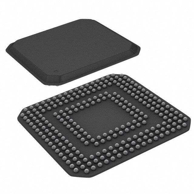
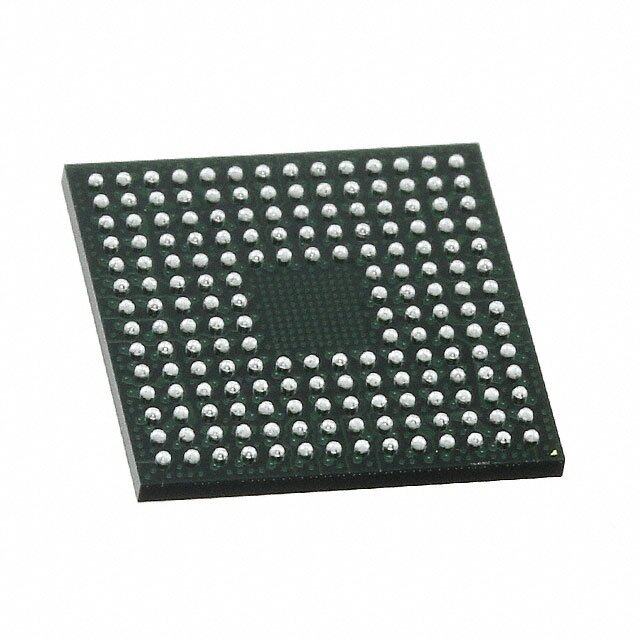
| 产品图片 |
|
| rohs | 符合RoHS无铅 / 符合限制有害物质指令(RoHS)规范要求 |
| 产品系列 | 接口 IC,PCI接口IC,Texas Instruments XIO1100ZGB- |
| NumberofLanes | 1 Lane |
| 数据手册 | |
| 产品型号 | XIO1100ZGB |
| PCN封装 | |
| 产品培训模块 | http://www.digikey.cn/PTM/IndividualPTM.page?site=cn&lang=zhs&ptm=9141 |
| 产品目录页面 | |
| 产品种类 | PCI接口IC |
| 供应商器件封装 | 100-BGA MICROSTAR(12.1x12.1) |
| 其它名称 | 296-20665 |
| 制造商产品页 | http://www.ti.com/general/docs/suppproductinfo.tsp?distId=10&orderablePartNumber=XIO1100ZGB |
| 包装 | 托盘 |
| 商标 | Texas Instruments |
| 安装类型 | 表面贴装 |
| 安装风格 | SMD/SMT |
| 封装 | Tray |
| 封装/外壳 | 100-LFBGA |
| 封装/箱体 | BGA-100 Microstar |
| 工作电源电压 | 3.3 V, 1.5 V, 1.8 V |
| 工厂包装数量 | 160 |
| 应用 | - |
| 接口 | TI-PIPE |
| 数据总线宽度 | 16 bit |
| 最大工作温度 | + 70 C |
| 最大数据速率 | 2.5 Gb/s |
| 最大时钟频率 | 125 MHz |
| 最小工作温度 | 0 C |
| 标准包装 | 160 |
| 电压-电源 | 1.35 V ~ 1.65 V,3 V ~ 3.6 V |
| 类型 | PCIe |
| 系列 | XIO1100 |
| 通道数 | 1 Lane |
| 配用 | /product-detail/zh/KS-ALT-2C35-30/649-1001-ND/1204738 |


- 商务部:美国ITC正式对集成电路等产品启动337调查
- 曝三星4nm工艺存在良率问题 高通将骁龙8 Gen1或转产台积电
- 太阳诱电将投资9.5亿元在常州建新厂生产MLCC 预计2023年完工
- 英特尔发布欧洲新工厂建设计划 深化IDM 2.0 战略
- 台积电先进制程称霸业界 有大客户加持明年业绩稳了
- 达到5530亿美元!SIA预计今年全球半导体销售额将创下新高
- 英特尔拟将自动驾驶子公司Mobileye上市 估值或超500亿美元
- 三星加码芯片和SET,合并消费电子和移动部门,撤换高东真等 CEO
- 三星电子宣布重大人事变动 还合并消费电子和移动部门
- 海关总署:前11个月进口集成电路产品价值2.52万亿元 增长14.8%


PDF Datasheet 数据手册内容提取
XIO1100 Data Manual Literature Number: SLLS690C April 2006 Revised August 2011
Contents Contents Section Page 1 XIO1100 Features . . . . . . . . . . . . . . . . . . . . . . . . . . . . . . . . . . . . . . . . . . . . . . . . . . . . . . . . . . . . . . . . . . . . . . . 1 2 Description . . . . . . . . . . . . . . . . . . . . . . . . . . . . . . . . . . . . . . . . . . . . . . . . . . . . . . . . . . . . . . . . . . . . . . . . . . . . 1 2.1 Ordering Information . . . . . . . . . . . . . . . . . . . . . . . . . . . . . . . . . . . . . . . . . . . . . . . . . . . . . . . . . . . . . . 1 2.2 Functional Description . . . . . . . . . . . . . . . . . . . . . . . . . . . . . . . . . . . . . . . . . . . . . . . . . . . . . . . . . . . . . 2 2.3 Power Management. . . . . . . . . . . . . . . . . . . . . . . . . . . . . . . . . . . . . . . . . . . . . . . . . . . . . . . . . . . . . . . 2 2.3.1 P0 . . . . . . . . . . . . . . . . . . . . . . . . . . . . . . . . . . . . . . . . . . . . . . . . . . . . . . . . . . . . . . . . . . . . 3 2.3.2 P0s . . . . . . . . . . . . . . . . . . . . . . . . . . . . . . . . . . . . . . . . . . . . . . . . . . . . . . . . . . . . . . . . . . . 3 2.3.3 P1 . . . . . . . . . . . . . . . . . . . . . . . . . . . . . . . . . . . . . . . . . . . . . . . . . . . . . . . . . . . . . . . . . . . . 3 2.4 Clock . . . . . . . . . . . . . . . . . . . . . . . . . . . . . . . . . . . . . . . . . . . . . . . . . . . . . . . . . . . . . . . . . . . . . . . . . . . 3 2.5 Reset . . . . . . . . . . . . . . . . . . . . . . . . . . . . . . . . . . . . . . . . . . . . . . . . . . . . . . . . . . . . . . . . . . . . . . . . . . . 3 2.6 Receiver Detection. . . . . . . . . . . . . . . . . . . . . . . . . . . . . . . . . . . . . . . . . . . . . . . . . . . . . . . . . . . . . . . . 4 2.7 Receiver Clock Tolerance Compensation. . . . . . . . . . . . . . . . . . . . . . . . . . . . . . . . . . . . . . . . . . . . . 4 2.8 Error Detection . . . . . . . . . . . . . . . . . . . . . . . . . . . . . . . . . . . . . . . . . . . . . . . . . . . . . . . . . . . . . . . . . . . 4 2.8.1 8B/10B Decode Error . . . . . . . . . . . . . . . . . . . . . . . . . . . . . . . . . . . . . . . . . . . . . . . . . . . . 5 2.8.2 Elastic Buffer Overflow Error . . . . . . . . . . . . . . . . . . . . . . . . . . . . . . . . . . . . . . . . . . . . . . 5 2.8.3 Elastic Buffer Underflow Error . . . . . . . . . . . . . . . . . . . . . . . . . . . . . . . . . . . . . . . . . . . . . 5 2.8.4 Disparity Error . . . . . . . . . . . . . . . . . . . . . . . . . . . . . . . . . . . . . . . . . . . . . . . . . . . . . . . . . . 5 2.9 Loopback . . . . . . . . . . . . . . . . . . . . . . . . . . . . . . . . . . . . . . . . . . . . . . . . . . . . . . . . . . . . . . . . . . . . . . . . 5 2.10 Electrical Idle. . . . . . . . . . . . . . . . . . . . . . . . . . . . . . . . . . . . . . . . . . . . . . . . . . . . . . . . . . . . . . . . . . . . . 5 2.11 Polarity Inversion . . . . . . . . . . . . . . . . . . . . . . . . . . . . . . . . . . . . . . . . . . . . . . . . . . . . . . . . . . . . . . . . . 5 2.12 Setting Negative Parity . . . . . . . . . . . . . . . . . . . . . . . . . . . . . . . . . . . . . . . . . . . . . . . . . . . . . . . . . . . . 5 2.13 Terminal Assignments . . . . . . . . . . . . . . . . . . . . . . . . . . . . . . . . . . . . . . . . . . . . . . . . . . . . . . . . . . . . . 6 2.14 Terminal Descriptions . . . . . . . . . . . . . . . . . . . . . . . . . . . . . . . . . . . . . . . . . . . . . . . . . . . . . . . . . . . . . 8 3 Electrical Characteristics . . . . . . . . . . . . . . . . . . . . . . . . . . . . . . . . . . . . . . . . . . . . . . . . . . . . . . . . . . . . . . . . 12 3.1 Absolute Maximum Ratings† . . . . . . . . . . . . . . . . . . . . . . . . . . . . . . . . . . . . . . . . . . . . . . . . . . . . . . . 12 3.2 Recommended Operating Conditions . . . . . . . . . . . . . . . . . . . . . . . . . . . . . . . . . . . . . . . . . . . . . . . . 12 3.3 PCI Express Differential Transmitter Output Ranges . . . . . . . . . . . . . . . . . . . . . . . . . . . . . . . . . . . 13 3.4 PCI Express Differential Receiver Input Ranges . . . . . . . . . . . . . . . . . . . . . . . . . . . . . . . . . . . . . . 15 3.5 Express Differential Reference Clock Input Ranges. . . . . . . . . . . . . . . . . . . . . . . . . . . . . . . . . . . . 18 3.6 Electrical Characteristics Over Recommended Operating Conditions (VDD_IO) . . . . . . . . . . . 19 3.7 Implementation−Specific Timing . . . . . . . . . . . . . . . . . . . . . . . . . . . . . . . . . . . . . . . . . . . . . . . . . . . . 19 4 Timing Diagrams . . . . . . . . . . . . . . . . . . . . . . . . . . . . . . . . . . . . . . . . . . . . . . . . . . . . . . . . . . . . . . . . . . . . . . . 20 5 Application Information . . . . . . . . . . . . . . . . . . . . . . . . . . . . . . . . . . . . . . . . . . . . . . . . . . . . . . . . . . . . . . . . . 24 5.1 Component Connection. . . . . . . . . . . . . . . . . . . . . . . . . . . . . . . . . . . . . . . . . . . . . . . . . . . . . . . . . . . . 24 5.2 XIO1100 Component Placement . . . . . . . . . . . . . . . . . . . . . . . . . . . . . . . . . . . . . . . . . . . . . . . . . . . . 25 5.3 Power Supply Filtering Recommendations . . . . . . . . . . . . . . . . . . . . . . . . . . . . . . . . . . . . . . . . . . . 25 5.4 PCIe Layout Guidelines . . . . . . . . . . . . . . . . . . . . . . . . . . . . . . . . . . . . . . . . . . . . . . . . . . . . . . . . . . . 27 5.5 PIPE Interface Layout Guidelines . . . . . . . . . . . . . . . . . . . . . . . . . . . . . . . . . . . . . . . . . . . . . . . . . . . 28 6 Mechanical Data . . . . . . . . . . . . . . . . . . . . . . . . . . . . . . . . . . . . . . . . . . . . . . . . . . . . . . . . . . . . . . . . . . . . . . . . 29 i
List of Figures Figure Page Figure 2−1. XIO1100 Functional Block Diagram . . . . . . . . . . . . . . . . . . . . . . . . . . . . . . . . . . . . . . . . . . . . . . . . . 2 Figure 4−1. TI−PIPE Input Timing . . . . . . . . . . . . . . . . . . . . . . . . . . . . . . . . . . . . . . . . . . . . . . . . . . . . . . . . . . . . . 20 Figure 4−2. TI−PIPE Data Output Timing . . . . . . . . . . . . . . . . . . . . . . . . . . . . . . . . . . . . . . . . . . . . . . . . . . . . . . . 21 Figure 4−3. TI−PIPE Output Functional Timing . . . . . . . . . . . . . . . . . . . . . . . . . . . . . . . . . . . . . . . . . . . . . . . . . . 22 Figure 4−4. TI−PIPE Input Functional Timing . . . . . . . . . . . . . . . . . . . . . . . . . . . . . . . . . . . . . . . . . . . . . . . . . . . 23 Figure 5−1. External Component Connections . . . . . . . . . . . . . . . . . . . . . . . . . . . . . . . . . . . . . . . . . . . . . . . . . . 24 Figure 5−2. Filter Designs . . . . . . . . . . . . . . . . . . . . . . . . . . . . . . . . . . . . . . . . . . . . . . . . . . . . . . . . . . . . . . . . . . . . 26 ii
List of Tables Table Page Table 2−1. Clock Selection . . . . . . . . . . . . . . . . . . . . . . . . . . . . . . . . . . . . . . . . . . . . . . . . . . . . . . . . . . . . . . . . . . . 3 Table 2−2. RX_STATUS Loopback Detection Code . . . . . . . . . . . . . . . . . . . . . . . . . . . . . . . . . . . . . . . . . . . . . . 4 Table 2−3. 100-pin GGB Signal Name Sorted by Terminal Number. . . . . . . . . . . . . . . . . . . . . . . . . . . . . . . . . 6 Table 2−4. 100-pin GGB Signal Name Sorted Alphabetically . . . . . . . . . . . . . . . . . . . . . . . . . . . . . . . . . . . . . . 7 Table 2−5. XIO1100 Terminals . . . . . . . . . . . . . . . . . . . . . . . . . . . . . . . . . . . . . . . . . . . . . . . . . . . . . . . . . . . . . . . 8 iii
Features 1 XIO1100 Features (cid:2) X1 PCI Express(cid:2) Serial Link (cid:2) TI-PIPE MAC Interface − PCI Express 1.1 Compliant − Source-Synchronous TX and RX Ports − Selectable Reference Clock (100 MHz, − 125 MHz TX/RX Clocks 125 MHz) − Selectable 16-Bit SDR or 8-Bit DDR Mode − Low-Power Capability (cid:2) 100-Pin MicroStar(cid:2) BGA Package (cid:2) Selectable 1.5−V or 1.8−V LVCMOS Buffers. TI and MicroStar BGA are trademarks of Texas Instruments Incorporated PCI Express is a trademark of PCI−SIG 2 Description The XIO1100 is a PCI Express(cid:3) PHY that is compliant with PCI Express Base Specification Revision 1.1 and that interfaces the PCI Express Media Access Layer (MAC) to a PCI Express serial link by using a modified version of the interface described in PHY Interface for the PCI Express(cid:2) Architecture (also known as PIPE interface) by Intel Corporation. This modified version of the PIPE interface is referred to as a TI-PIPE interface throughout this data manual. The TI-PIPE interface is a pin-configurable interface that can be configured as either a 16-bit or an 8-bit interface. • The 16-bit TI-PIPE interface is a 125 MHz 16-bit parallel interface with a 16-bit output bus (RXDATA) that is clocked by the RXCLK output clock and a 16-bit input bus (TXDATA) that is clocked by the TXCLK input clock. Both buses are clocked using Single Data Rate (SDR) clocking in which the data transitions are on the rising edge of the associated clock. • The 8-bit TI-PIPE interface is a 250 MHz 8-bit parallel interface with an 8-bit output bus (RXDATA) that is clocked by the RXCLK output clock and an 8-bit input bus (TXDATA) that is clocked by the TXCLK input clock. Both buses are clocked using Double Data Rate (DDR) clocking in which the data transitions are on both the rising edge and the falling edge of the clock. The XIO1100 PHY interfaces to a 2.5 Gbps PCI Express serial link with a transmit differential pair (TXP and TXN) and a receive differential pair (RXP and RXN). Incoming data at the XIO1100 PHY receive differential pair (RXP and RXN) is forwarded to the MAC on the RXDATA output bus. Data received from the MAC on the TXDATA input bus is forwarded to the XIO1100 PHY transfer differential pair (TXP and TXN). The XIO1100 is also responsible for handling the 8B/10B encoding/decoding and scrambling/unscrambling of the outgoing data. In addition, XIO1100 can recover/interpolate the clock on the receiver side based on the transitions guaranteed by the use of the 8B/10B mechanism and supply this to the receive side of the data link layer logic. In addition to the TI-PIPE interface, the XIO1100 has some TI-proprietary side-band signals that some customers may wish to use to take advantage of additional XIO1100 low-power state features (for example, disabling the PLL during the L1 power state). 2.1 Ordering Information ORDERING NUMBER VOLTAGE TEMPERATURE PACKAGE XIO1100 3.3/1.8/1.5 0°C to 70°C 100-terminal GGB June 2006 Revised August 2011 SLLS690C 1
Description 2.2 Functional Description The XIO1100 meets all of the requirements for a PCI−Express PHY as defined by Section 4, Physical Layer Specifications, of the PCI−SIG document PCI Express Base Specification. The XIO1100 conforms to the functional behavior described in PHY Interface for the PCI Express(cid:2) Architecture by Intel Corporation. There are only two differences between the XIO1100 TI−PIPE interface and the Intel PIPE interface. The PIPE interface uses a single SDR clock source to clock both the RXDATA and the TXDATA. The TI−PIPE interface uses two source synchronous clocks, RX_CLK and TX_CLK, to clock the RXDATA and TXDATA. RXDATA uses RX_CLK and TXDATA uses TX_CLK. In the 8-bit mode, the TI−PIPE interface is a DDR (Double Data Rate) interface. In the 16-bit mode, it is an SDR (Single Data Rate) interface. The PIPE interface is always an SDR interface. Figure 2−1 shows a functional block diagram of the XIO1100. REFCLK/REFCLK− PLL TX_DATA 16/8 TXP/TXN TX_CLK TX BLOCK TX_DATAK[1:0] STATUS COMMAND RX_DATA 16/8 RXP/RXN RX_CLK RX BLOCK RX_DATAK[1:0] Figure 2−1. XIO1100 Functional Block Diagram 2.3 Power Management The three power states are: • P0 • P0s • P1 2 SLLS690C June 2006 Revised August 2011
Description 2.3.1 P0 P0 is the normal operation state for the XIO1100. The POWERDOWN[1:0] input signals define which of the three power states that an XIO110 is in at any given time. In states P0, P0s, and P1, the XIO1100 is required to keep P_CLK operational. For all state transitions between these three states, the XIO1100 indicates successful transition into the designated power state by a single cycle assertion of PHY_STATUS. For all power state transitions, the MAC must not begin any operational sequence or more power state transitions until the XIO1100 has indicated that the initial state transition is finished. P2 state and beacon are not supported. In the P0 state, all internal clocks in the XIO1100 are operational. P0 is the only state where the XIO1100 transmits and receives PCI Express signaling. P0 is the appropriate PHY power management state for most states in the Link Training and Status State Machine (LTSSM). Exceptions are listed as follows for each lower power XIO1100 state. 2.3.2 P0s In the P0s state, RX_CLK output stays operational. The MAC moves the XIO1100 to this state only when the transmit channel is idle. P0s state is used when the transmitter is in state Tx_L0s.Idle. If the receiver detects an electrical idle while the XIO1100 is in either P0 or P0s power states, the receiver portion of the XIO1100 takes appropriate power saving measures. 2.3.3 P1 In the P1 state, selected internal clocks in the XIO1100 will be turned off. RX_CLK output will stay operational. The MAC moves the XIO1100 to this state only when both transmit and receive channels are idle. The XIO1100 does not indicate successful entry into P1 (by asserting PhyStatus) until RX_CLK is stable and the operating dc common mode voltage is stable and within specification (in accordance with PCI Express Base Specification). P1 is used for the Disabled state, all Detect states, and L1.Idle state of the Link Training and Status State Machine (LTSSM). While in P1 state, the optional P1_SLEEP input signal can be used to reduce even more power consumption by disabling the RX_CLK signal. However, the P1_SLEEP input must not be asserted when the XIO1100 is in any state other than P1 state, and the XIO1100 must not be transitioned out of the P1 state as long as P1_SLEEP is asserted. 2.4 Clock The RX_CLK of XIO1100 is derived from the REFCLK input. A 100 MHz differential clock or a 125 MHz single ended clock can be used as the source clock. The frequency selection is determined by CLK_SEL. If CLK_SEL is low during /RESET transitioning from a low state to a high state, the source clock at REFCLK+/REFCLK− is a 100 MHz differential clock. If CLK_SEL is high during /RESET transitioning from a low state to a high state, the source clock at REFCLK+ is a 125 MHz single ended clock. In this case, REFCLK− needs to be tied to VSS. Table 2−1. Clock Selection RX_CLK CLK_SEL = 0 100 MHz differential clock CLK_SEL = 1 125 MHz single ended clock 2.5 Reset When the MAC resets the XIO1100 (initial power on), the MAC must hold the XIO1100 in reset until power and REFCLK to the XIO1100 are stable. The XIO1100 signals that RX_CLK is valid (RX_CLK has been running at its operational frequency for at least one clock), and the XIO1100 is in the specified power state by the de−assertion of PhyStatus. While Reset# is asserted, the MAC must have TxDetectRx/Loopback de−asserted, TxElecIdle asserted, TxCompliance de−asserted, RxPolarity de−asserted, and PowerDown = P1. June 2006 Revised August 2011 SLLS690C 3
Description 2.6 Receiver Detection While in the P1 power state, XIO1100 can be instructed to perform a receiver detection operation to determine if there is a receiver at the other end of the link. The MAC requests XIO1100 to do a receiver detect sequence by asserting TXDETECTRX/LOOPBACK high. Upon completion of the receiver detection operation, the XIO1100 asserts PHY_STATUS high for one RX_CLK cycle. While PHY_STATUS is high, XIO1100 drives the proper receiver status code onto the RX_STATUS[2:0] signals according to Table 2−2. After the receiver detection has completed (as signaled by the assertion of PhyStatus), the MAC must de−assert TxDetectRx/Loopback before initiating another receiver detection or a power state transition. Table 2−2. RX_STATUS Loopback Detection Code RX_STATUS[2:0] RECEIVER STATUS 000 Receiver not present 011 Receiver present NOTE: TX_DET_LOOPBACK must remain asserted until XIO1100 asserts the PHY_STATUS. 2.7 Receiver Clock Tolerance Compensation The XIO1100 receiver contains an elastic buffer that compensates for differences in frequencies between bit rates at the two ends of a link. The elastic buffer is capable of holding at least seven symbols to tolerate worst-case differences (600ppm) in frequency and worst-case intervals between SKP ordered-sets, where an SKP order-set is a set of symbols transmitted as a group. The first symbol of a SKP ordered-set is a COM (0xBC) and is followed by three SKP (0x1C) symbols. The purpose of SKP ordered-sets is to allow the receiving device (in this case, XIO1100) to adjust the data stream that is being received to prevent the elastic buffer from either overflowing or underflowing due to any differences between the clocking frequencies of the transmitting device and the receiving device. The XIO1100 monitors the data stream received at the RXP/RXN differential pair for SKP ordered-sets. When the XIO1100 detects that an SKP ordered-set is being received, it either adds or removes SKP symbols from the data stream, depending on the current state of the elastic buffer. If the elastic buffer is in danger of underflowing, SKP symbols are added to the ordered-set before it is loaded into the buffer. If the elastic buffer is in danger of overflowing, SKP symbols are removed from the ordered-set before it is loaded into the buffer. When the XIO1100 detects a SKP ordered-set, the XIO1100 asserts an Add SKP code (001b) on the RX_STATUS[2:0] bus in the same RX_CLK cycle that it asserts the COM (0xBC) symbol on the RX_DATA[15:0] bus, if it is adding a SKP symbol to the data stream. In the case of removing an SKP symbol, the XIO1100 asserts the Remove SKP code (010b) to the RX_STATUS[2:0] when the COM symbol is asserted. 2.8 Error Detection If a detectable receive error occurs, the appropriate error code is asserted on the RX_STATUS[2:0] pins for one RX_CLK cycle as close as possible to the point in the data stream where the error occurred. There are four error conditions that can be encoded on the RXSTATUS signals. If more than one error happens to occur on a received byte (or set of bytes transferred across a 16-bit interface), the errors are signaled with the following priority: • 8B/10B decode error • Elastic buffer overflow • Elastic buffer underflow • Disparity error If an error occurs during a SKP ordered-set, such that the error code and the SKP code occur concurrently, the error code has priority over the SKP code. 4 SLLS690C June 2006 Revised August 2011
Description 2.8.1 8B/10B Decode Error When XIO1100 detects an 8B/10B decode error, it asserts an EDB (0xFE) symbol in the data on the RX_DATA[15:0] where the bad byte occurred (only the erroneous byte is replaced with the EDB symbol; the other byte is still valid data). In the same RX_CLK clock cycle that the EDB symbol is asserted on the RX_DATA[15:0] bus, the 8B/10B decode error code (100b) is asserted on the RX_STATUS[2:0] bus. Since the 8B/10B decoding error has priority over all other receive error codes, it could mask out a disparity error occurring on the other byte of data being clocked onto the RX_DATA[15:0] with the EDB symbol. 2.8.2 Elastic Buffer Overflow Error When the elastic buffer overflows, data is lost during reception. XIO1100 generates an elastic buffer overflow error when this occurs. The elastic buffer overflow error code (101b) is asserted on the RX_STATUS[2:0] on the RX_CLK clock cycle that the omitted data would have been asserted. The remaining data asserted on the RX_DATA[15:0]] bus is still valid data, but the elastic buffer overflow error code on the RX_STATUS[2:0] just marks a discontinuity point in the data stream being received. 2.8.3 Elastic Buffer Underflow Error When the elastic buffer underflows, EDB (0xFE) symbols are inserted into the data stream on the RX_DATA[15:0] bus to fill the holes created by the gaps between valid data. For every RX_CLK clock cycle, an EDB symbol is asserted on the RX_DATA[15:0] bus, and an elastic buffer underflow error code (111b) is asserted on the RX_STATUS[2:0] bus. 2.8.4 Disparity Error When the XIO1100 detects a disparity error, it asserts a disparity error code (111b) on the RX_STATUS[2:0] bus in the same RX_CLK clock cycle that it asserts the erroneous data on the RX_DATA[15:0] bus. However, it is not possible to discern which byte had the disparity error. 2.9 Loopback The XIO1100 begins a loopback operation when the MAC asserts TX_DET_LOOPBACK while holding TX_ELECIDLE de−asserted. The XIO1100 stops transmitting data to the TXP/TXN signaling pair from the TI−PIPE interface and begins transmitting the data received at the RXP/RXN signaling pair on the TXP/TXN signaling pair. This data is not routed through the 8B/10B coding/encoding paths. While in the loopback operation, the received data is still sent to the RXDATA[15:0] bus of the TI−PIPE interface. The data sent to the RXDATA[15:0] bus is routed through the 10B/8B decoder. The XIO1100 terminates the loopback operation and returns to transmitting TXDATA[15:0] over the TXP/TXN signaling pair when the TX_DET_LOOPBACK signal is de−asserted. 2.10 Electrical Idle The XIO1100 expects the MAC to issue the required COM (K28.5) symbol and the required number of IDL symbols (K28.3) on TXDATA[7:0] before asserting the TX_ELECTRICAL signal. The XIO1100 meets the requirements of the Electrical Requirements of a PCI Express PHY (for these requirements, see Section 4.3.1.9, Electrical Idle, and Table B−2 in Appendix B of PCI Express Base Specification Revision 1.1). 2.11 Polarity Inversion Polarity inversion can happen in many places in the receive chain, including somewhere in the serial path, as symbols are placed into the elastic buffer or as symbols are removed from the elastic buffer. The XIO1100 inverts the data received on the RXP/RXN signaling pair when RxPolarity is asserted. The inverted data will begin showing up on the RXDATA within 20 RX_CLKS of when RxPolarity is asserted. 2.12 Setting Negative Parity To set the running disparity to negative, TxCompliance is asserted for one clock cycle that matches with the data that is to be transmitted with negative disparity. June 2006 Revised August 2011 SLLS690C 5
Description 2.13 Terminal Assignments The XIO1100 is packaged in a 100-pin GGB BGA package. See Section 6 for GGB-package terminal diagram. Table 2−3 lists the terminal assignments in terminal-number order with corresponding signal names for the GGB package. Table 2−4 lists the terminal assignments arranged in alphanumerical order by signal name with corresponding terminal numbers for the GGB package. Table 2−3. 100-pin GGB Signal Name Sorted by Terminal Number GGB SIGNAL NAME GGB SIGNAL GGB SIGNAL NAME GGB SIGNAL NAME NUMBER NUMBER NAME NUMBER NUMBER A3 RX_DATA8 C9 RESERVED G11 VSSA L6 CLK_SEL A4 RX_DATA9 C10 VSSA G12 TXP L7 VDD_IO A5 RX_DATA11 C12 RXN G13 TXN L8 VSS A6 RX_DATA13 C13 RXP H1 TX_DATA13 L9 POWERDOWN1 A7 RX_DATA15 D1 RX_DATA4 H2 TX_DATA14 L10 DDR_EN A8 RX_DATAK0 D2 RX_DATA5 H3 RX_VALID L12 VDD_15_COMB A9 RESERVED D3 VSS H11 VDD_33_COMB L13 VDD_33_COM_IO A10 RESERVED D11 VDDA_33 H12 VDDA_15 M3 TX_DATA6 A11 REFCLK− D12 VSSA H13 VDDA_15 M4 TX_DATA5 B3 RX_ELECIDLE D13 VSSA J1 TX_DATA11 M5 TX_DATA3 B4 RX_DATA10 E1 RX_DATA2 J2 TX_DATA12 M6 TX_DATA1 B5 RX_DATA12 E2 RX_DATA3 J3 VSS M7 TX_DATAK1 B6 RX_DATA14 E3 RX_STATUS0 J11 VSS M8 TX_CLK B7 RX_DATAK1 E11 VDDA_15 J12 VDDA_33 M9 POWERDOWN0 B8 RX_CLK E12 VSSA J13 VDDA_33 M10 P1_SLEEP B9 RESERVED E13 VDD_15 K1 TX_DATA9 M11 VREG_PD B10 RESERVED F1 RX_DATA0 K2 TX_DATA10 N3 TX_DATA7 B11 REFCLK+ F2 RX_DATA1 K3 VDD_IO N4 TX_DATA4 C1 RX_DATA7 F3 VDD_IO K11 VSSA N5 TX_DATA2 C2 RX_DATA6 F11 VDD_15 K12 R0 N6 TX_DATA0 C4 VSS F12 VSS K13 R1 N7 TX_DATAK0 C5 VDD_IO F13 VSSA L1 TX_DATA8 N8 TXCOMPLIANCE C6 RX_POLARITY G1 RX_STATUS1 L2 VSS N9 TXELECIDLE C7 VDD_15_CORE G2 TX_DATA15 L4 VDD_15_CORE N10 PHY_STATUS C8 VSS G3 RX_STATUS2 L5 TXDETECTRX/L N11 RESETN OOPBACK 6 SLLS690C June 2006 Revised August 2011
Description Table 2−4. 100-pin GGB Signal Name Sorted Alphabetically SIGNAL NAME GGB SIGNAL NAME GGB SIGNAL NAME GGB SIGNAL NAME GGB NUMBER NUMBER NUMBER NUMBER CLK_SEL L6 RX_DATA8 A3 TX_DATA6 M3 VDD_IO F3 P1_SLEEP M10 RX_DATA9 A4 TX_DATA7 N3 VDD_IO K3 DDR_EN L10 RX_DATA10 B4 TX_DATA8 L1 VDD_IO L7 PHY_STATUS N10 RX_DATA11 A5 TX_DATA9 K1 VDD_IO C5 POWERDOWN0 M9 RX_DATA12 B5 TX_DATA10 K2 VDDA_15 H12 POWERDOWN1 L9 RX_DATA13 A6 TX_DATA11 J1 VDDA_15 E11 R0 K12 RX_DATA14 B6 TX_DATA12 J2 VDDA_15 H13 R1 K13 RX_DATA15 A7 TX_DATA13 H1 VDDA_33 J13 REFCLK− A11 RX_DATAK0 A8 TX_DATA14 H2 VDDA_33 D11 REFCLK+ B11 RX_DATAK1 B7 TX_DATA15 G2 VREG_PD M11 RESERVED B9 RX_ELECIDLE B3 TX_DATAK0 N7 VSS D3 RESERVED A10 RX_POLARITY C6 TX_DATAK1 M7 VSS J3 RESERVED B10 RX_STATUS0 E3 TXCOMPLIANCE N8 VSS L2 RESERVED A9 RX_STATUS1 G1 TXDETECTRX/ L5 VSS L8 LOOPBACK RESERVED C9 RX_STATUS2 G3 TXELECIDLE N9 VSS J11 /RESET N11 RX_VALID H3 TXN G13 VSS F12 RX_CLK B8 RXN C12 TXP G12 VSS C8 RX_DATA0 F1 RXP C13 VDD_15 F11 VSS C4 RX_DATA1 F2 TX_CLK M8 VDD_15 E13 VSSA K11 RX_DATA2 E1 TX_DATA0 N6 VDD_15_COMB L12 VSSA G11 RX_DATA3 E2 TX_DATA1 M6 VDD_15_CORE L4 VSSA F13 RX_DATA4 D1 TX_DATA2 N5 VDD_15_CORE C7 VSSA E12 RX_DATA5 D2 TX_DATA3 M5 VDDA_33 J12 VSSA D13 RX_DATA6 C2 TX_DATA4 N4 VDD_33_COM_IO L13 VSSA D12 RX_DATA7 C1 TX_DATA5 M4 VDD_33_COMB H11 VSSA C10 June 2006 Revised August 2011 SLLS690C 7
Description 2.14 Terminal Descriptions Table 2−5 describes the XIO1100 terminals. The terminals are grouped by functionality. Table 2−5. XIO1100 Terminals TERMINAL I/O DESCRIPTION NAME NO. PIPE INTERFACE /RESET N11 I Reset the device. This signal is active low and asynchronous. POWERDOWN[1:0] L9, M9 I Power State Control: Value: Description 00: P0, normal operation (used for all Polling, Configuration, Recovery, Loop−back, and Hot-Reset states, and the L0 state of the LTSSM) 01: P0s, low recovery time latency, power−saving state (used for the TX_L0s.idle state of the LTSSM) 10: P1, longer recovery time (64μs max) latency, lower power state (used for the disabled state, all detect states, and the L1.idle state of the LTSSM) PHY_STATUS N10 O Used to communicate completion of several PHY functions, including power management state transitions and receiver detection TX_CLK M8 I Synchronous input clock for TX_DATA[15:0] and TX_DATAK[1:0] inputs If the DDR_EN signal is low during /RESET transitioning from a low state to a high state, TX_CLK is a SDR clock and TX_DATA[15:0] and TX_DATAK[1:0] are latched on the rising edge of TX_CLK. If the DDR_EN signal is high during /RESET transitioning from a low state to a high state, TX_CLK is a DDR clock and TX_DATA[7:0] and TX_DATAK[0] are latched on both the rising and the falling edge of TX_CLK.TX_DATA[15:8] and TX_DATAK[1] are not used. TX_DATA[15:0] G2, H2, H1, J2, I Parallel Data Transmit Bus J1, K2, K1, L1, If the DDR_EN signal is low during /RESET transitioning from a low state to a high N3, M3, M4, state, TX_DATA[15:0] is latched off the bus on the rising edge of TX_CLK. N4, M5, N5, TX_DATA[7:0] represents the first symbol and TX_DATA[15:8] represents the M6, N6 second symbol to be transmitted over the TXN and TXP differential signal pair. If the DDR_EN signal is high during /RESET transitioning from a low state to a high state, TX_DATA[7:0] is latched off the bus on both edges of the TX_CLK. TX_DATA[15:8] is not used and should be grounded. The data on TX_DATA[7:0] during the rising edge of the clock represents the first symbol and data on TX_DATA[7:0] during the falling edge of the clock represents the second symbol to be transmitted over the TXN and TXP differential signal pair. TX_DATAK[1:0] M7, N7 I Data/Control for the Parallel Data Transmit Bus If the DDR_EN signal is low during /RESET transitioning from a low state to a high state, TX_DATAK[0] corresponds to the TX_DATA[7:0] and TX_DATAK[1] to TX_DATA[15:8]. If the DDR_EN signal is high during /RESET transitioning from a low state to a high state, the state of TX_DATAK[0] corresponds to the data on the TX_DATA[7:0] bus during the same phase of the clock. TX_DATAK[1] is not used and should be grounded. A value of zero indicates that the corresponding TXDATA bits contain data information; a value of one indicates that the corresponding TXDATA bits contain a control byte. NOTE: The TI−PIPE interface can operate at either 1.5 V or 1.8 V, depending on the voltage level of VDD_IO. If VDD_IO is 1.5 V, the TI−PIPE interface operates at 1.5 V level. If VDD_IO is 1.8 V, the TI−PIPE interface operates at 1.8 V level. 8 SLLS690C June 2006 Revised August 2011
Description Table 2−5. XIO1100 Terminals (Continued) TERMINAL I/O DESCRIPTION TX_ELECIDLE N9 I Forces TXN/TXP outputs to electrical idle. When de−asserting low while in P0 state (POWERDOWN[1:0] = 00), indicates that valid data is on the TXDATA bus and that this data should be transmitted. When asserted high while in P0s state (POWERDOWN[1:0] = 01), always asserted for P0s state. When asserted high while in P1 state (POWERDOWN[1:0] = 10), always asserted for P1 state. TX_COMPLIANCE N8 I Transmit Compliance Pattern When asserted high, the XIO1100 sets the running disparity to negativity. Used when transmitting the compliance pattern. TX_DET_LOOPBACK L5 I Begin Receive Detect/Begin Loop−Back Input to device to either begin a receive detect operation or enter loop−back mode. RX_CLK B8 O Synchronous Output Clock for RX_DATA[15:0] and RX_DATAK[1:0] outputs If the DDR_EN signal is low during /RESET transitioning from a low state to a high state, RX_CLK is a SDR clock, and RX_DATA[15:0] and RX_DATAK[1:0] are latched on the rising edge of RX_CLK. If the DDR_EN signal is high during /RESET transitioning from a low state to a high state, RX_CLK is a DDR clock and RX_DATA[7:0] and RX_DATAK[0] are latched on both the rising and falling edge of the RX_CLK. RX_DATA[15:8] and RX_DATAK[1] are not used. RX_CLK is also used as the internal PCLK for the XIO1100. RX_DATA[15:0] A7, B6, A6, B5, O Parallel Data Receive Bus A5, B4, A4, A3, If the DDR_EN signal is low during /RESET transitioning from a low state to a high C1, C2, D2, D1, state, RX_DATA[15:0] is latched on the rising edge of the RX_CLK. RX_DATA[7:0] E2, E1, F2, F1 represents the first symbol received, and RX_DATA[15:8] represents the second symbol received from the RXN and RXP differential signal pair. If the DDR_EN signal is high during /RESET transitioning from a low state to a high state, RX_DATA[7:0] is latched on both the rising edge and falling edge of the RX_CLK. The data on RX_DATA[7:0] during the rising edge of the RX_CLK represents the first symbol received, and the data on RX_DATA[7:0] during the falling edge of the RX_CLK represents the second symbol received from the RXN and RXP differential signal pair. RX_DATA[15:8] is not used. RX_DATAK[1:0] B7, A8 O Data/Control for the parallel data receive bus If the DDR_EN signal is low during /RESET transitioning from a low state to a high state, the state of RX_DATAK[0] corresponds to RX_DATA[7:0], and RX_DATAK[1] corresponds to RX_DATA[15:8]. If the DDR_EN signal is high during /RESET transitioning from a low state to a high state, the state of RX_DATA[0] corresponds to the data on RX_DATA[7:0] during the same phase of the clock. RX_DATAK[1] is not used. A value of zero indicates that the corresponding RXDATA bits contain data information. A value of one indicates that the corresponding RXDATA bits contain a control byte. NOTE: The TI−PIPE interface can operate at either 1.5 V or 1.8 V, depending on the voltage level of VDD_IO. If VDD_IO is 1.5 V, the TI−PIPE interface operates at 1.5 V level. If VDD_IO is 1.8 V, the TI−PIPE interface operates at 1.8 V level. June 2006 Revised August 2011 SLLS690C 9
Description Table 2−5. XIO1100 Terminals (Continued) TERMINAL I/O DESCRIPTION RX_STATUS[2:0] G3, G1, E3 O Encodes receiver status and error codes for the received data stream and receive detection, as follows: Value: Description 000: Received data ok 001: 1 SKP added 010: 1 SKP removed 011: Receiver detected 100: 8B/10B decode error 101: Elastic buffer overflow 110: Elastic buffer underflow 111: Receive disparity error RX_VALID H3 O Indicates symbol lock and valid data on RX_DATA[15:0] and RX_DATAK[1:0] RX_POLARITY C6 I Instructs the XIO1100 to perform polarity inversion on the RXN and RXP differential signal pair. Asserting a high on this signal instructs the XIO1100 to perform the polarity inversion. RX_ELECIDLE B3 O Indicates receiver detection of an electrical idle of the RXP and RXN signal pair. This is an asynchronous signal. REFERENCE CLOCK PIN REFCLK+ B11 I The positive and negative terminals for the input reference clock. If CLK_SEL is low REFCLK− A11 during /RESET transitioning from low to high, a 100 MHz clock source has to be applied to REFCLK+ and REFCLK−. If CLK_SEL is high during /RESET transitioning from low to high, a 125 MHz clock source has to be applied to REFCLK+. REFCLK− is not used and should be grounded. R0 K12 I Terminals for a 14.56KÙ 1% resistors (recommended 5.90K and 8.66K resistors in R1 K13 series) TRANSMIT AND RECEIVE PIN TXP G12 O PCI express link differential pair TX positive terminal TXN G13 O PCI express link differential pair TX negative terminal RXP C13 I PCI express link differential pair RX positive terminal. The XIO1100 has integrated 50-Ω termination resistor to VSS on the RXP terminal, eliminating the need for external components. RXN C12 I PCI express link differential pair RX negative terminal. The XIO1100 has integrated 50-Ω termination resistor to VSS on the RXN terminal, eliminating the need for external components. MISC P1_SLEEP M10 I P1 low-power enable. This input, when asserted high, enables a low−power mode when the XIO1100 enters the P1 state. If the input is asserted when the power−down state is P1 (POWERDOWN[1:0] = 10), the device enters a low−power mode. In this mode, the PLL is disabled and the RX_CLK is unavailable. The P1_SLEEP input must not be asserted when the XIO1100 is in any state other than P1 state and the XIO1100 must not be transitioned out of the P1 state as long as P1_SLEEP is asserted. NOTE: The TI−PIPE interface can operate at either 1.5 V or 1.8 V, depending on the voltage level of VDD_IO. If VDD_IO is 1.5 V, the TI−PIPE interface operates at 1.5 V level. If VDD_IO is 1.8 V, the TI−PIPE interface operates at 1.8 V level. 10 SLLS690C June 2006 Revised August 2011
Description Table 2−5. XIO1100 Terminals (Continued) TERMINAL I/O DESCRIPTION CLK_SEL L6 I Clock Select This input, when asserted low during /RESET transitioning from low to high, selects the 100 MHz differential clock source. A 100MHz clock source has to be applied to REFCLK+ and REFCLK−. This input, when asserted high during /RESET transitioning to high, selects the 125MHz single ended clock source. A 125 MHz clock source has to be applied to REFCLK+. REFCLK− has to be connected to VSS. VREG_PD M11 I This pin must be pulled to GND during normal operation. DDR_EN L10 I DDR_EN This input, when asserted high during /RESET transitioning to low state to high state, defines the TI−PIPE interface to be a 8−bit DDR interface; otherwise, it is an 16-bit SDR interface. Value: Description 1: DDR_EN is an 8−bit DDR interface 0: DDR_EN is a 16−bit SDR interface RESERVED RESERVED B9 RESERVED RESERVED A10 RESERVED RESERVED B10 RESERVED RESERVED A9 RESERVED RESERVED C9 RESERVED. This pin needs to be pulled to GND during normal operation. POWER SUPPLY TERMINALS VDD_15 E13, F11 PWR 1.5−V digital power supply. VDD_15_CORE C7, L4 PWR 1.5−V core voltage. VDDA_15 E11, H12, H13 PWR 1.5−V analog power supply. VDD_15_COMB L12 PWR 1.5−V main power output. It should be connected to a filter network of 0.01μF, 1μF, and 1000pF capacitors. VDDA_33 D11, J12, J13 PWR 3.3−V analog power supply. VDD_33_COMB H11 PWR 3.3−V main output. It should be connected to a filter network of 0.01μF, 1μF, and 1000pF capacitors. VDD_33_COMB_IO L13 PWR 3.3−V I/O output. It should be connected to a filter network of 0.01μF, 1μF, and 1000pF capacitors. VDD_IO C5, F3, K3, L7 PWR Power supply for digital I/O. Can be either 1.5 V or 1.8 V depending on desired signaling level. VSS D3, J3, L2, L8, GND Digital ground. J11, F12, C4, C8 VSSA K11, G11, F13, GND Analog ground. E12, D13, D12, C10 NOTE: The TI−PIPE interface can operate at either 1.5 V or 1.8 V, depending on the voltage level of VDD_IO. If VDD_IO is 1.5 V, the TI−PIPE interface operates at 1.5 V level. If VDD_IO is 1.8 V, the TI−PIPE interface operates at 1.8 V level. June 2006 Revised August 2011 SLLS690C 11
Electrical Characteristics 3 Electrical Characteristics 3.1 Absolute Maximum Ratings† Supply voltage range: 3.3 V Supply . . . . . . . . . . . . . . . . . . . . . . . . . . . . . . . . . . . . . . . . . . . . . −0.5 V to 3.6 V 1.8 V Supply . . . . . . . . . . . . . . . . . . . . . . . . . . . . . . . . . . . . . . . . . . . . −0.5 V to 1.95 V 1.5 V Supply . . . . . . . . . . . . . . . . . . . . . . . . . . . . . . . . . . . . . . . . . . . . −0.5 V to 1.65 V Input voltage range, V: PCI Express (RX) . . . . . . . . . . . . . . . . . . . . . . . . . . . . . . . . . . . . . . –0.6 V to 0.6 V I V: PCI Express REFCLK (single-ended) . . . . . . . . . . . –0.5 V to V + 0.5 V I DDA_33 V: PCI Express REFCLK (differential) . . . . . . . . . . . . . . . –0.5 V toV + 0.5 V I DD_15 Input clamp current, (V < 0 or V > V ) (see Note 1). . . . . . . . . . . . . . . . . . . . . . . . . . . . . . . . . . . . . . ±20 mA I I DD Output clamp current, (V < 0 or V > V ) (see Note 2) . . . . . . . . . . . . . . . . . . . . . . . . . . . . . . . . . . ±20 mA O O DD Human body model (HBM) ESD performance . . . . . . . . . . . . . . . . . . . . . . . . . . . . . . . . . . . . . . . . . . . . . 1500 V Charged device model (CDM) ESD performance . . . . . . . . . . . . . . . . . . . . . . . . . . . . . . . . . . . . . . . . . . . 500 V Storage temperature range, Tstg . . . . . . . . . . . . . . . . . . . . . . . . . . . . . . . . . . . . . . . . . . . . . . . . –65°C to 150°C † Stresses beyond those listed under absolute maximum ratings may cause permanent damage to the device. These are stress ratings only, and functional operation of the device at these or any other conditions beyond those indicated under recommended operating conditions is not implied. Exposure to absolute-maximum-rated conditions for extended periods may affect device reliability. NOTES: 1. Applies for external input and bidirectional buffers. VI < 0 or VI > VDD. 2. Applies to external output and bidirectional buffers. VO < 0 or VO > VDD. 3.1.1 Current Consumption MODE TX RX VDDIO VDD15 VDD33 UNITS L0 on on 89 102 5.4 mA idle on 89 81 1.3 mA L0s on idle 66 93 4.3 mA idle idle 66 72 1.3 mA on idle 66 94 4.3 mA L1 idle idle 65 72 1.3 mA L1_sleep 75 10 1.3 mA 3.2 Recommended Operating Conditions OPERATION MIN NOM MAX UNIT VDD_15 VDDA_15 SSuuppppllyy vvoollttaaggee 11..55 VV 11..3355 11..55 11..6655 VV VDD_15_CORE VDDA_33 Supply voltage 3.3 V 3 3.3 3.6 V VDD_IO (1.5 V) Supply voltage (I/O) 1.5V 1.35 1.5 1.65 V VDD_IO (1.8 V) Supply voltage (I/O) 1.8V 1.65 1.8 1.95 V TA Operating ambient temperature range 0 25 70 °C TJ Virtual junction temperature (Note 3) 0 25 115 °C NOTES: 3. The junction temperature reflects simulated conditions. The customer is responsible for verifying junction temperature. NOTE: The TI−PIPE interface can operate either at 1.5 V or 1.8 V, depending on the voltage level of VDD_IO. If VDD_IO is 1.5 V, the TI−PIPE interface operates at 1.5 V level. If VDD_IO is 1.8 V, the TI−PIPE interface operates at 1.8 V level. 12 SLLS690C June 2006 Revised August 2011
Electrical Characteristics 3.3 PCI Express Differential Transmitter Output Ranges PARAMETER TERMINALS MIN NOM MAX UNIT COMMENTS UI TXP, TXN 399.88 400 400.12 ps Each UI is 400 ps ±300 ppm. UI does not account for Unit interval SSC−dictated variations. See Note 4. VTX–DIFFp–p TXP, TXN 0.8 1.2 V VTX–DIFFp–p = 2*|VTXP − VTXN| Differential peak–to– See Note 5. peak output voltage VTX–DE–RATIO De–em- TXP, TXN −3.0 −3.5 −4.0 dB This is the ratio of the VTX–DIFFp–p of the second and phasized differential following bits after a transition divided by the output voltage (ratio) VTX–DIFFp–p of the first bit after a transition. See Note 5. TTX–EYE TXP, TXN 0.75 UI The maximum transmitter jitter can be derived as Minimum TX eye width TTXMAX– JITTER = 1 − TTX–EYE = 0.3 UI See Notes 5 and 6. TTX–EYE–MEDIAN–to– TXP, TXN 0.15 UI Jitter is defined as the measurement variation of the MAX–JITTER crossing points (VTX–DIFFp–p = 0 V) in relation to recov- Maximum time between ered TX UI. A recovered TX UI is calculated over 3500 the jitter median and consecutive UIs of sample data. Jitter is measured us- maximum deviation ing all edges of the 250 consecutive UIs in the center of from the median the 3500 UIs used for calculating the TX UI. See Notes 5 and 6. TTX–RISE, TXP, TXN 0.125 UI See Notes 5 and 8. TTX–FALL P/N TX output rise/fall time VTX–CM–ACp TXP, TXN 20 mV VTX–CM–ACp = RMS(|VTXP + VTXN|/2 – VTX–CM–DC) RMS ac peak common VTX–CM–DC = DC(avg) of |VTXP + VTXN|/2 mode output voltage See Note 5. VTX–CM–DC–ACTIVE– TXP, TXN 0 100 mV |VTX–CM–DC – VTX–CM–Idle–DC| ≤ 100 mV IDLE–DELTA VTX–CM–DC = DC(avg) of |VTXP + VTXN|/2 [during L0] Absolute delta of dc VTX–CM–Idle–DC = DC(avg) of |VTXP + VTXN|/2 [during common mode voltage electrical idle] during L0 and electrical See Note 5. idle. VTX–CM–DC–LINE–DELTA TXP, TXN 0 25 mV |VTXP–CM–DC – VTXN–CM–DC| ≤ 25 mV when Absolute delta of dc VTXP–CM–DC = DC(avg) of |VTXP| common mode voltage VTXN–CM–DC = DC(avg) of |VTXN| between P and N See Note 5. NOTES: 4. No test load is necessarily associated with this value. 5. Specified at the measurement point into a timing and voltage compliance test load and measured over any 250 consecutive TX UIs. 6. A TTX–EYE = 0.75 UI provides for a total sum of deterministic and random jitter budget of TTX–JITTER–MAX = 0.25 UI for the transmitter collected over any 250 consecutive TX UIs. The TTX–EYE–MEDIAN–to–MAX–JITTER specification ensures a jitter distribution in which the median and the maximum deviation from the median is less than half of the total TX jitter budget collected over any 250 consecutive TX UIs. It must be noted that the median is not the same as the mean. The jitter median describes the point in time where the number of jitter points on either side is approximately equal, as opposed to the averaged time value. 7. The transmitter input impedance results in a differential return loss greater than or equal to 12 dB and a common mode return loss greater than or equal to 6 dB over a frequency range of 50 MHz to 1.25 GHz. This input impedance requirement applies to all valid input levels. The reference impedance for return loss measurements is 50 Ω to ground for both the P and N lines. Note that the use of the series capacitors CTX is optional for the return loss measurement. 8. Measured between 20% and 80% at transmitter package terminals into a test load for both VTXP and VTXN June 2006 Revised August 2011 SLLS690C 13
Electrical Characteristics PARAMETER TERMINALS MIN NOM MAX UNIT COMMENTS VTX–IDLE–DIFFp TXP, TXN 0 20 mV VTX–IDLE–DIFFp = |VTXP–Idle − VTXN–Idle| ≤ 20 mV Electrical idle differen- See Note 5. tial peak output voltage VTX–RCV–DETECT TXP, TXN 600 mV The total amount of voltage change that a transmitter The amount of voltage can apply to sense whether a low impedance receiver is change allowed during present. receiver detection VTX–DC–CM TXP, TXN 0 3.6 V The allowed dc common mode voltage under any con- The TX dc common dition. mode voltage ITX–SHORT TXP, TXN 90 mA Total current the transmitter can provide when shorted TX short circuit current to its ground limit TTX–IDLE–MIN TXP, TXN 50 UI Minimum time a transmitter must be in electrical Idle. Minimum time spent in Utilized by the receiver to start looking for an electrical electrical idle idle exit after successfully receiving an electrical idle ordered set. TTX–IDLE–SET–to–IDLE TXP, TXN 20 UI After sending an electrical idle ordered set, the transmit- Maximum time to ter must meet all electrical idle specifications within this transition to a valid time. This is considered a debounce time for the trans- electrical idle after mitter to meet electrical idle after transitioning from L0. sending an electrical idle ordered set TTX–IDLE–to–DIFF–DATA TXP, TXN 20 UI Maximum time to meet all TX specifications when tran- Maximum time to sitioning from electrical idle to sending differential data. transition to valid TX This is considered a debounce time for the TX to meet specifications after all TX specifications after leaving electrical idle. leaving an electrical idle condition RLTX–DIFF TXP, TXN 10 dB Measured over 50 MHz to 1.25 GHz. See Note 7. Differential return loss RLTX–CM TXP, TXN 6 dB Measured over 50 MHz to 1.25 GHz. See Note 7. Common mode return loss ZTX–DIFF–DC TXP, TXN 80 100 120 Ω TX dc differential mode low impedance DC differential TX impedance NOTES: 4. No test load is necessarily associated with this value. 5. Specified at the measurement point into a timing and voltage compliance test load and measured over any 250 consecutive TX UIs. 6. A TTX–EYE = 0.75 UI provides for a total sum of deterministic and random jitter budget of TTX–JITTER–MAX = 0.25 UI for the transmitter collected over any 250 consecutive TX UIs. The TTX–EYE–MEDIAN–to–MAX–JITTER specification ensures a jitter distribution in which the median and the maximum deviation from the median is less than half of the total TX jitter budget collected over any 250 consecutive TX UIs. It must be noted that the median is not the same as the mean. The jitter median describes the point in time where the number of jitter points on either side is approximately equal, as opposed to the averaged time value. 7. The transmitter input impedance results in a differential return loss greater than or equal to 12 dB and a common mode return loss greater than or equal to 6 dB over a frequency range of 50 MHz to 1.25 GHz. This input impedance requirement applies to all valid input levels. The reference impedance for return loss measurements is 50 Ω to ground for both the P and N lines. Note that the use of the series capacitors CTX is optional for the return loss measurement. 8. Measured between 20% and 80% at transmitter package terminals into a test load for both VTXP and VTXN 14 SLLS690C June 2006 Revised August 2011
Electrical Characteristics PARAMETER TERMINALS MIN NOM MAX UNIT COMMENTS ZTX–DC TXP, TXN 40 Ω Required TXP as well as TXN dc impedance during all Transmitter dc imped- states ance CTX TXP, TXN 75 200 nF All transmitters are ac–coupled and are required on the AC coupling capacitor PWB. NOTES: 4. No test load is necessarily associated with this value. 5. Specified at the measurement point into a timing and voltage compliance test load and measured over any 250 consecutive TX UIs. 6. A TTX–EYE = 0.75 UI provides for a total sum of deterministic and random jitter budget of TTX–JITTER–MAX = 0.25 UI for the transmitter collected over any 250 consecutive TX UIs. The TTX–EYE–MEDIAN–to–MAX–JITTER specification ensures a jitter distribution in which the median and the maximum deviation from the median is less than half of the total TX jitter budget collected over any 250 consecutive TX UIs. It must be noted that the median is not the same as the mean. The jitter median describes the point in time where the number of jitter points on either side is approximately equal, as opposed to the averaged time value. 7. The transmitter input impedance results in a differential return loss greater than or equal to 12 dB and a common mode return loss greater than or equal to 6 dB over a frequency range of 50 MHz to 1.25 GHz. This input impedance requirement applies to all valid input levels. The reference impedance for return loss measurements is 50 Ω to ground for both the P and N lines. Note that the use of the series capacitors CTX is optional for the return loss measurement. 8. Measured between 20% and 80% at transmitter package terminals into a test load for both VTXP and VTXN 3.4 PCI Express Differential Receiver Input Ranges PARAMETER TERMINALS MIN NOM MAX UNIT COMMENTS UI RXP, RXN 399.88 400 400.12 ps Each UI is 400 ps ±300 ppm. UI does not account Unit interval for SSC−dictated variations. See Note 9. VRX–DIFFp–p RXP, RXN 0.175 1.200 V VRX–DIFFp–p = 2*|VRXP − VRXN| Differential input peak–to–peak See Note 10. voltage TRX–EYE RXP, RXN 0.4 UI The maximum interconnect media and transmitter Minimum receiver eye width jitter that can be tolerated by the receiver is derived as TRX–MAX–JITTER = 1 − TRX–EYE = 0.6 UI. See Notes 10 and 11. NOTES: 9. No test load is necessarily associated with this value. 10. Specified at the measurement point and measured over any 250 consecutive UIs. A test load must be used as the RX device when taking measurements. If the clocks to the RX and TX are not derived from the same reference clock, the TX UI recovered from 3500 consecutive UI is used as a reference for the eye diagram. 11. A TRX–EYE = 0.40 UI provides for a total sum of 0.60 UI deterministic and random jitter budget for the transmitter and interconnect collected any 250 consecutive UIs. The TRX–EYE–MEDIAN–to–MAX–JITTER specification ensures a jitter distribution in which the median and the maximum deviation from the median is less than half of the total UI jitter budget collected over any 250 consecutive TX UIs. It must be noted that the median is not the same as the mean. The jitter median describes the point in time where the number of jitter points on either side is approximately equal, as opposed to the averaged time value. If the clocks to the RX and TX are not derived from the same reference clock, the TX UI recovered from 3500 consecutive UIs must be used as the reference for the eye diagram. 12. The receiver input impedance results in a differential return loss greater than or equal to 15 dB with the P line biased to 300 mV and the N line biased to −300 mV and a common mode return loss greater than or equal to 6 dB (no bias required) over a frequency range of 50 MHz to 1.25 GHz. This input impedance requirement applies to all valid input levels. The reference impedance for return loss measurements is 50 Ω to ground for both the P and N line (i.e., as measured by a Vector Network Analyzer with 50–Ω probes). The use of the series capacitors CTX is optional for the return loss measurement. 13. Impedance during all link training status state machine (LTSSM) states. When transitioning from a PCI Express reset to the detect state (the initial state of the LTSSM), there is a 5–ms transition time before receiver termination values must be met on the unconfigured lane of a port. 14. The RX dc common mode impedance that exists when no power is present or PCI Express reset is asserted. This helps ensure that the receiver detect circuit does not falsely assume a receiver is powered on when it is not. This term must be measured at 300 mV above the RX ground. June 2006 Revised August 2011 SLLS690C 15
Electrical Characteristics PARAMETER TERMINALS MIN NOM MAX UNIT COMMENTS TRX–EYE–MEDIAN–to–MAX–JITTER RXP, RXN 0.3 UI Jitter is defined as the measurement variation of the Maximum time between the crossing points (VRX–DIFFp–p = 0 V) in relation to jitter median and maximum recovered TX UI. A recovered TX UI is calculated deviation from the median over 3500 consecutive UIs of sample data. Jitter is measured using all edges of the 250 consecutive UIs in the center of the 3500 UIs used for calculating the TX UI. See Notes 10 and 11. VRX–CM–ACp RXP, RXN 150 mV VRX–CM–ACp = RMS(|VRXP + VRXN|/2 – VRX–CM–DC) AC peak common mode input VRX–CM–DC = DC(avg) of |VRXP + VRXN|/2 voltage See Note 10. RLRX–DIFF RXP, RXN 10 dB Measured over 50 MHz to 1.25 GHz with the P and Differential return loss N lines biased at +300 mV and −300 mV, respective- ly. See Note 12. RLRX–CM RXP, RXN 6 dB Measured over 50 MHz to 1.25 GHz with the P and Common mode return loss N lines biased at +300 mV and −300 mV, respective- ly. See Note 12. ZRX–DIFF–DC RXP, RXN 80 100 120 Ω RX dc differential mode impedance. DC differential input impedance See Note 13. ZRX–DC RXP, RXN 40 50 60 Ω Required RXP as well as RXN dc impedance (50 Ω DC input impedance ±20% tolerance). See Notes 10 and 13. ZRX–HIGH–IMP–DC RXP, RXN 200k Ω Required RXP as well as RXN dc impedance when Powered−down dc input the receiver terminations do not have power. impedance See Note 14. NOTES: 9. No test load is necessarily associated with this value. 10. Specified at the measurement point and measured over any 250 consecutive UIs. A test load must be used as the RX device when taking measurements. If the clocks to the RX and TX are not derived from the same reference clock, the TX UI recovered from 3500 consecutive UI is used as a reference for the eye diagram. 11. A TRX–EYE = 0.40 UI provides for a total sum of 0.60 UI deterministic and random jitter budget for the transmitter and interconnect collected any 250 consecutive UIs. The TRX–EYE–MEDIAN–to–MAX–JITTER specification ensures a jitter distribution in which the median and the maximum deviation from the median is less than half of the total UI jitter budget collected over any 250 consecutive TX UIs. It must be noted that the median is not the same as the mean. The jitter median describes the point in time where the number of jitter points on either side is approximately equal, as opposed to the averaged time value. If the clocks to the RX and TX are not derived from the same reference clock, the TX UI recovered from 3500 consecutive UIs must be used as the reference for the eye diagram. 12. The receiver input impedance results in a differential return loss greater than or equal to 15 dB with the P line biased to 300 mV and the N line biased to −300 mV and a common mode return loss greater than or equal to 6 dB (no bias required) over a frequency range of 50 MHz to 1.25 GHz. This input impedance requirement applies to all valid input levels. The reference impedance for return loss measurements is 50 Ω to ground for both the P and N line (i.e., as measured by a Vector Network Analyzer with 50–Ω probes). The use of the series capacitors CTX is optional for the return loss measurement. 13. Impedance during all link training status state machine (LTSSM) states. When transitioning from a PCI Express reset to the detect state (the initial state of the LTSSM), there is a 5–ms transition time before receiver termination values must be met on the unconfigured lane of a port. 14. The RX dc common mode impedance that exists when no power is present or PCI Express reset is asserted. This helps ensure that the receiver detect circuit does not falsely assume a receiver is powered on when it is not. This term must be measured at 300 mV above the RX ground. 16 SLLS690C June 2006 Revised August 2011
Electrical Characteristics PARAMETER TERMINALS MIN NOM MAX UNIT COMMENTS VRX–IDLE–DET–DIFFp–p RXP, RXN 65 175 mV VRX–IDLE–DET–DIFFp–p = 2*|VRXP − VRXN| measured Electrical idle detect threshold at the receiver package terminals TRX–IDLE–DET–DIFF–ENTER–TIME RXP, RXN 10 ms An unexpected electrical idle (VRX–DIFFp–p < Unexpected electrical idle enter VRX–IDLE–DET–DIFFp–p) must be recognized no lon- detect threshold integration ger than TRX–IDLE–DET–DIFF–ENTER–TIME to signal an time unexpected idle condition. NOTES: 9. No test load is necessarily associated with this value. 10. Specified at the measurement point and measured over any 250 consecutive UIs. A test load must be used as the RX device when taking measurements. If the clocks to the RX and TX are not derived from the same reference clock, the TX UI recovered from 3500 consecutive UI is used as a reference for the eye diagram. 11. A TRX–EYE = 0.40 UI provides for a total sum of 0.60 UI deterministic and random jitter budget for the transmitter and interconnect collected any 250 consecutive UIs. The TRX–EYE–MEDIAN–to–MAX–JITTER specification ensures a jitter distribution in which the median and the maximum deviation from the median is less than half of the total UI jitter budget collected over any 250 consecutive TX UIs. It must be noted that the median is not the same as the mean. The jitter median describes the point in time where the number of jitter points on either side is approximately equal, as opposed to the averaged time value. If the clocks to the RX and TX are not derived from the same reference clock, the TX UI recovered from 3500 consecutive UIs must be used as the reference for the eye diagram. 12. The receiver input impedance results in a differential return loss greater than or equal to 15 dB with the P line biased to 300 mV and the N line biased to −300 mV and a common mode return loss greater than or equal to 6 dB (no bias required) over a frequency range of 50 MHz to 1.25 GHz. This input impedance requirement applies to all valid input levels. The reference impedance for return loss measurements is 50 Ω to ground for both the P and N line (i.e., as measured by a Vector Network Analyzer with 50–Ω probes). The use of the series capacitors CTX is optional for the return loss measurement. 13. Impedance during all link training status state machine (LTSSM) states. When transitioning from a PCI Express reset to the detect state (the initial state of the LTSSM), there is a 5–ms transition time before receiver termination values must be met on the unconfigured lane of a port. 14. The RX dc common mode impedance that exists when no power is present or PCI Express reset is asserted. This helps ensure that the receiver detect circuit does not falsely assume a receiver is powered on when it is not. This term must be measured at 300 mV above the RX ground. June 2006 Revised August 2011 SLLS690C 17
Electrical Characteristics 3.5 Express Differential Reference Clock Input Ranges PARAMETER TERMINALS MIN NOM MAX UNIT COMMENTS fIN–DIFF REFCLK+ 100 MHz The input frequency is 100 MHz + 300 ppm and Differential input fre- − 2800 ppm including SSC–dictated variations. REFCLK− quency fIN–SE REFCLK+ 125 MHz The input frequency is 125 MHz + 300 ppm and Single–ended input − 300 ppm. frequency VRX–DIFFp–p REFCLK+ 0.175 1.200 V VRX–DIFFp–p = 2*|VREFCLK+ − VREFCLK−| Differential input REFCLK− peak–to–peak voltage VIH–SE REFCLK+ 0.7 VDD_33 VDD_33 V Single–ended, reference clock mode high-level input voltage VIL–SE REFCLK+ 0 0.3 VDD_33 V Single–ended, reference clock mode low-level input voltage VRX–CM–ACp REFCLK+ 140 mV VRX–CM–ACp = RMS(|VREFCLK+ + VREFCLK−|/2 – AC peak common VRX–CM–DC) REFCLK− mode input voltage VRX–CM–DC = DC(avg) of |VREFCLK+ + VREFCLK−|/2 Duty cycle REFCLK+ 40% 60% Differential and single–ended waveform input duty cycle REFCLK− ZRX–DIFF–DC REFCLK+ 20 kΩ REFCLK+/− dc differential mode impedance DC differential input REFCLK− impedance ZRX–DC REFCLK+ 20 kΩ REFCLK+ dc single–ended mode impedance DC input impedance REFCLK− NOTE 15:The XIO1100 is compliant with the defined system jitter models for a PCI–Express reference clock and associated TX/RX link. These system jitter models are described in the PCI–Express Jitter Modeling, Revision 1.0RD document. Any usage of the XIO1100 in a system configuration that does not conform to the defined system jitter models requires the system designer to validate the system jitter budgets. 18 SLLS690C June 2006 Revised August 2011
Electrical Characteristics 3.6 Electrical Characteristics Over Recommended Operating Conditions (V ) DD_IO TEST PARAMETER OPERATION MIN TYP MAX UNIT CONDITIONS VIH High-level input voltage (Note 16) VDD_IO 0.7 VDD_IO VDD_IO V VIL Low-level input voltage (Note 16) VDD_IO 0 0.3 VDD_IO V VI Input voltage 0 VDD_IO V VO Output voltage (Note 17) 0 VDD_IO V tT Input transition time (trise and tfall) 0 25 ns VOH High-level output voltage VDD_IO IOH = −8 mA 0.8 VDD_IO V VOL Low-level output voltage VDD_IO IOL = 8 mA 0.22 VDD_IO V IOH High−level output current −8 mA IOL Low−level output current 8 mA IOZ High-impedance, output current VDD_IO VI = 0 to VDD_IO ±20 μA (Note 17) II Input current (Note 18) VDD_IO VI = 0 to VDD_IO ±1 μA NOTES:16. Applies to external inputs and bidirectional buffers. 17. Applies to external outputs and bidirectional buffers. 18. Applies to external input buffers. 3.7 Implementation−Specific Timing TIMING DESCRIPTION NORM MAX Transmit Time for data moving between the parallel interface and the PCI Express serial lines. Timing is 29.2 ns 33.2 ns Latency measured from when the data is transferred across the parallel interface (i.e., the rising edge of TX_CLK) and when the first bit of the equivalent 10−bit symbol is transmitted on the Tx+/Tx− serial lines. Receive Time for data moving between the parallel interface and the PCI Express serial lines. Timing is 77.2 ns 93.2 ns Latency measured from when the first bit of a 10−bit symbol is available on the Rx+/Rx− serial lines to when the corresponding 8−bit data is transferred across the parallel interface (i.e., the rising edge of RX_CLK). Loopback Amount of time that the XIO1100 requires to begin looping back receive data. Duration is from 25.2 ns 29.2 ns Enable Latency when TxDetectRx/Loopback is asserted until the receive data is being transmitted on the serial pins. N_FTS with Number of FTS ordered sets required by the receiver to obtain reliable bit and symbol lock when 23 23 Common Clock operating with a common clock. N_FTS without Number of FTS ordered sets required by the receiver to obtain reliable bit and symbol lock when 255 255 Common Clock operating without a common clock. XIO1100 Lock Amount of time required for the XIO1100 receiver to obtain reliable bit and symbol lock after 2.0 μs 4.0 μs Time valid TSx ordered−sets are present at the receiver. P0s to P0 Amount of time required for the XIO1100 to return to the P0 state after having been in the P0s 28.0 ns 32.0 ns Transitioning state. Time is measured from when the MAC sets the PowerDown signals to P0 until the Time XIO1100 asserts PhyStatus. The XIO1100 asserts PhyStatus when it is ready to begin data transmission and reception. P1 to P0 Amount of time required for the XIO1100 to return to the P0 state after having been in the P1 28.0 ns 32.0 ns Transitioning state. Time is measured from when the MAC sets the PowerDown signals to P0 until the Time XIO1100 asserts PhyStatus. The XIO1100 asserts PhyStatus when it is ready to begin data transmission and reception. Reset to Ready Timed from when Reset# is de−asserted until the XIO1100 de−asserts PHY_STATUS. 10.0 ns 11.0 ns Time June 2006 Revised August 2011 SLLS690C 19
Timing Diagrams 4 Timing Diagrams TI−PIPE Input Timing t cyc TX_CLK TxData[7:0] (DDR mode) TxDataK[0] (DDR mode) t t fsu rsu t t fh fh TxData[15:0] (SDR mode) TxDataK[1:0] (SDR mode) TxDetectRx/Loopback TxElecIdle TxCompliance RxPolarity PowerDown[1:0] t rsu t fh Figure 4−1. TI−PIPE Input Timing PARAMETER DESCRIPTION VALUE tcyc Period, TX_CLK 8 ns (TYP) trsu Input Setup to TX_CLK rising 1.3 ns (MAX) trh Input Hold from TX_CLK rising 0.1 ns (MIN) tfsu Input Setup to TX_CLK falling 1.3 ns (MAX) tfh Input Hold from TX_CLK falling 0.1 ns (MIN) 20 SLLS690C June 2006 Revised August 2011
Timing Diagrams TI−PIPE Data Output Timing t cyc RX_CLK RxData[7:0] (DDR mode) RxDataK[0] (DDR mode) t t t rco fh fh t fco RxData[15:0] (SDR mode) RxDataK[1:0] (SDR mode) RxValid PhyStatus RxElecIdle RxStatus[2:0] t rco t fh Figure 4−2. TI−PIPE Data Output Timing PARAMETER DESCRIPTION VALUE tcyc Period, RX_CLK 8.0 ns (TYP) trco Clock to output, RX_CLK rising 2.0 ns (MAX) trh Output hold, RX_CLK rising 0.7 ns (MIN) tfco Clock to output, RX_CLK falling 2.0 ns (MAX) tfh Output hold, RX_CLK falling 0.7 ns (MIN) June 2006 Revised August 2011 SLLS690C 21
Timing Diagrams TI−PIPE Output Functional Timing RX_CLK RxData[7:0] (DDR mode) SYMBOL (N) SYMBOL (N+1) RxDataK[0] (DDR mode) RxData[15:0] (SDR mode) RxData[7:0] − SYMBOL (N) RxDataK[1:0] (SDR mode) RxData[15:8] − SYMBOL (N+1) RxValid PhyStatus RxElecIdle RxStatus[2:0] Figure 4−3. TI−PIPE Output Functional Timing 22 SLLS690C June 2006 Revised August 2011
Timing Diagrams TI−PIPE Input Functional Timing TX_CLK TxData[7:0] (DDR mode) SYMBOL (N) SYMBOL (N+1) TxDataK[0] (DDR mode) TxData[15:0] (SDR mode) TxData[7:0] − SYMBOL (N) TxDataK[1:0] (SDR mode) TxData[15:8] − SYMBOL (N+1) TxDetectRx/Loopback TxElecIdle TxCompliance RxPolarity PowerDown[1:0] Figure 4−4. TI−PIPE Input Functional Timing June 2006 Revised August 2011 SLLS690C 23
Application Information 5 Application Information 5.1 Component Connection Details regarding connection of components to the various terminals of the XIO1100 are discussed primarily in entries for each terminal in the terminal functions table. 3.3VA 1.5VA 1.5VD 1.5V_1.8VD C1 C2 C3 TXN U1 J13D11J12 H13H12E11 L4C7F11E13 L7K3F3C5 1uF 0.01uF 1000pF G13 TXP G12 TTXXNP A_33A_33A_33 A_15A_15A_15 OREORED_15D_15 D_IOD_IOD_IOD_IO VDD_33_COMB H11 C4 C5 C6 RRXXNP CC1123 RRXXNP VDDVDDVDD VDDVDDVDD _15_C_15_CVDVD VDVDVDVD VDD_33_COM_IO L13 1uF 0.01uF 1000pF DD A11 DD REFCLKN B11 REFCLKN VV L12 REFCLKP REFCLKP VDD_15_COMB C7 C8 C9 CLK_SEL L6 CLK_SEL (0=100MHz Diff 1=125MHz Single) 1uF 0.01uF 1000pF R1 5.90K (1%) K12 R2 8.66K (1%) K13 R0 RX_CLK B8 RX_CLK TTTTTTTTRPPPDXXXXXXXX1OOED_________SRWWSCDDDDDDDE_EELLAAAAAAAETERRKTTTTTTTNNAAAAAAAEDD0123456POOWWNN01 MNLMMNMNMNMMN1L1116543909865430 PDPPRRTTTTTTTTXXXXXXXX1OOD1E_________SRWWSCDDDDDDDE_EELLAAAAAAAETERRKTTTTTTTNNAAAAAAAEDD 0123456P(OO1=WW8NNb01it 0TS=16bit) OUTPUTS RRRRRRRRRRRRRRRRXXXXXXXXXXXXXXXX________________DDDDDDDDDDDDDDDDAAAAAAAAAAAAAAAATTTTTTAAAAAATTTTTTTTTTAAAAAAAAAA1111111012345678902345 FFBABABAEEDDCCAA1245566712341221 RRRRRRRRRRRRRRRRXXXXXXXXXXXXXXXX________________DDDDDDDDDDDDDDDDAAAAAAAAAAAAAAAATTTTTTTTTTTTTTTTAAAAAAAAAAAAAAAA0123456789111111102345 TTTXXX___DDDAAATTTAAA789 KKL211 TTTXXX___DDDAAATTTAAA789 NPU RRXX__DDAATTAAKK01 AB87 RRXX__DDAATTAAKK01 TTTTXXXX____DDDDAAAATTTTAAAA11111023 HHJJ1212 TTTTXXXX____DDDDAAAATTTTAAAA11111023 I RRRXXX___SSSTTTAAATTTUUUSSS012 EGG313 RRRXXX___SSSTTTAAATTTUUUSSS012 TTTXXX___DDDAAATTTAAA11K450 GNM727 TTTXXX___DDDAAATTTAAA11K450 RXP_HERYLXSE_TCVAAITDLULISDE NBH3130 RRPHXX__YVESALTELAICTDUIDSLE TX_DATAK1 TX_DATAK1 A9 N8 RSVD B10 TTTXXXCDELOEETMCEPICDLTILARENXCE CNL695 TTTXXXDCELEOETMCEPICDLTILARENXC / ELOOPBACK AAAAAAA G_PD RRRSSSVVVDDD BAC9190 RX_POLARITY RX_POLARITY SSSSSSSS SSSSSSS E RSVD SSSSSSSS SSSSSSS R VVVVVVVV VVVVVVV V XIO1100GGB C4C8D3F12J11J3L2L8 C10D12D13E12F13G11K11 M11 Figure 5−1. External Component Connections Figure 5−1 does not show the decoupling capacitors for the power supplies. Texas Instruments recommends using at least one 0.1 μF capacitor for each power supply pin. In addition to the 0.1 μF capacitor, Texas Instruments recommends adding 0.01 μF and 0.001 μF capacitors for each analog power supply pin. Texas Instruments also recommends isolating the analog power from the digital power. 24 SLLS690C June 2006 Revised August 2011
Application Information 5.2 XIO1100 Component Placement The filter network on VDD_33_COMB, VDD_33_COMB_IO, and VDD_15_COMB needs to be placed as close as possible to each pin (specifically H11, L13, and L12). It is recommended that the trace width for these three pins be at least 10 mils. The R0 and R1 terminals connect to an external resistor to set the drive current for the PCI Express TX driver. The recommended resistor value is 14,560-Ω with 1% tolerance. A 14,560-Ω resistor is a custom value. To eliminate the need for a custom resistor, two series resistors are recommended: a 5,900-Ω 1% resistor and an 8,660-Ω 1% resistor. Trace lengths must be kept short to minimize noise coupling into the reference resistor terminals. 5.3 Power Supply Filtering Recommendations To meet the PCI Express jitter specifications, low-noise power supplies are required on several of the XIO1100 voltage terminals. The power terminals that require low-noise power include VDDA_15 and VDDA_33. This section provides guidelines for the filter design to create low-noise power sources. The least expensive solution for low-noise power sources is to filter existing 3.3 V and 1.5 V power supplies. This solution requires analysis of the noise frequencies present on the power supplies. The XIO1100 has external interfaces operating at clock rates of 100 MHz, 125 MHz, 250 MHz, and 2.5 GHz. Other devices located near the XIO1100 may produce switching noise at different frequencies. Also, the power supplies that generate the 3.3 V and 1.5 V power rails may add low frequency ripple noise. Linear regulators have feedback loops that typically operate in the 100 kHz range. Switching power supplies typically have operating frequencies in the 500 kHz range. When analyzing power supply noise frequencies, the first, third, and fifth harmonic of every clock source should be considered. Critical analog circuits within the XIO1100 must be shielded from this power-supply noise. The fundamental requirement for a filter design is to reduce power-supply noise to a peak-to-peak amplitude of less than 25mV. This maximum noise amplitude should apply to all frequencies from 0 Hz to 12.5 GHz. The following information should be considered when designing a power supply filter: 1. Ideally, the series resonance frequency for each filter component should be greater than the fifth harmonic of the maximum clock frequency. With a maximum clock frequency of 1.25 GHz, the third harmonic is 3.75GHz and the fifth harmonic is 6.25 GHz. Finding inductors and capacitors with a series resonance frequency above 6.25 GHz is both difficult and expensive. Components with a series resonance frequency in the 4 to 6 GHz range are a good compromise. 2. The inductor(s) associated with the filter must have a dc resistance low enough to pass the required current for the connected power terminals. The voltage drop across the inductor must be low enough to meet the minus 10% voltage margin requirement associated with each XIO1100 power terminal. Power supply output voltage variation must be considered, as well as voltage drops associated with any connector pins and circuit board power distribution geometries. 3. The Q versus frequency curve associated with the inductor must be appropriate to reduce power terminal noise to less than the maximum peak−to−peak amplitude requirement for the XIO1100. Recommending a specific inductor is difficult, because every system design is different and therefore the noise frequencies and noise amplitudes are different. Many factors influence the inductor selection for the filter design. Power supplies must have adequate input and output filtering. A sufficient number of bulk and bypass capacitors is required to minimize switching noise. Assuming that board level power is properly filtered and minimal low frequency noise is present, frequencies less than 10 MHz, an inductor with a Q greater than 20 from approximately 10 MHz to 3 GHz should be adequate for most system applications. 4. The series component(s) in the filter may either be an inductor or a ferrite bead. Testing has been performed on both component types. When measuring PCI Express link jitter, the inductor or ferrite bead solutions produce equal results. When measuring circuit board EMI, the ferrite bead is a superior solution. June 2006 Revised August 2011 SLLS690C 25
Application Information 5. When designing filters associated with power distribution, the power supply is a low-impedance source, and the device power terminals are a low-impedance load. The best filter for this application is a T filter. See Figure 5−2 for a T filter circuit. Some systems may require this type of filter design if the power supplies or nearby components are exceptionally noisy. This type of filter design is recommended if a significant amount of low frequency noise (frequencies less than 10 MHz) is present in a system. 6. For most applications a Pi filter is adequate. See Figure 5−2 for a Pi filter circuit. When implementing a Pi filter, the two capacitors and the inductor must be located next to each other on the circuit board and must be connected together with wide, low impedance traces. Capacitor ground connections must be short and low-impedance. 7. If a significant amount of high frequency noise (frequencies greater than 300 MHz) is present in a system, creating an internal circuit board capacitor helps reduce this noise. This capacitor is accomplished by locating power and ground planes next to each other in the circuit board stack-up. A gap of 0.003 mils between the power and ground planes significantly reduces this high frequency noise. 8. Another option for filtering high-frequency logic noise is to create an internal board capacitor using signal layer copper plates. When a component requires a low-noise power supply, usually the Pi filter is located near the component. A plate capacitor may be created directly under the Pi filter. In the circuit board stack-up, select a signal layer that is physically located next to a ground plane. Then, generate an internal 0.25 inch by 0.25 inch plate on that signal layer. Assuming a 0.006 mil gap between the signal layer plate and the internal ground plane, this arrangement generates a 12 pF capacitor. By connecting this plate capacitor to the trace between the Pi filter and the component’s power terminals, an internal circuit board high frequency bypass capacitor is created. This solution is extremely effective for switching frequencies above 300 MHz. Figure 5−2 illustrates two different filter designs that may be used with the XIO1100 to provide low-noise power to critical power terminals. POWER SUPPLY COMPONENT SIDE SIDE Pi FILTER DESIGN POWER SUPPLY COMPONENT SIDE SIDE T FILTER DESIGN Figure 5−2. Filter Designs 26 SLLS690C June 2006 Revised August 2011
Application Information 5.4 PCIe Layout Guidelines The XIO1100 TXP and TXN terminals comprise a low-voltage, 100-Ω differentially driven signal pair. The RXP and RXN terminals for the XIO1100 receive a low-voltage, 100-Ω differentially driven signal pair. The XIO1100 has integrated 50-Ω termination resistors to VSS on both the RXP and RXN terminals, eliminating the need for external components. Each lane of the differential signal pair must be ac-coupled. The recommended value for the series capacitor is 0.1 μF. To minimize stray capacitance associated with the series capacitor circuit board solder pads, 0402-sized capacitors are recommended. When routing a 2.5-Gb/s low-voltage, 100-Ω differentially driven signal pair, the following circuit board design guidelines must be considered: 1. The PCI Express drivers and receivers are designed to operate with adequate bit error rate margins over a 20” maximum length signal pair routed through FR4 circuit board material. 2. Each differential signal pair must be 100-Ω differential impedance with each single-ended lane measuring in the range of 50-Ω to 55-Ω impedance to ground. 3. The differential signal trace lengths associated with a PCI Express high-speed link must be length matched to minimize signal jitter. This length-matching requirement applies only to the P and N signals within a differential pair. The transmitter differential pair does not need to be length matched to the receiver differential pair. The absolute maximum trace length difference between the TXP signal and TXN signal must be less than 5 mils. This value also applies to the RXP and RXN signal pair. 4. If a differential signal pair is broken into segments by vias, series capacitors, or connectors, the length of the positive signal trace must be length matched to the negative signal trace for each segment. Trace length differences over all segments are additive and must be less than 5 mils. 5. The location of the series capacitors is critical. For add-in cards, the series capacitors are located between the TXP/TXN terminals and the PCI Express connector. In addition, the capacitors are placed near the PCI Express connector. This translates to two capacitors on the motherboard for the downstream link, and two capacitors on the add-in card for the upstream link. If both the upstream device and the downstream device reside on the same circuit board, the capacitors are located near the TXP/TXN terminals for each link. 6. The number of vias must be minimized. Each signal trace via reduces the maximum trace length by approximately 2 inches. For example: if 6 vias are needed, the maximum trace length is 8 inches. 7. When routing a differential signal pair, 45-degree angles are preferred over 90-degree angles. Signal trace length matching is easier with 45-degree angles, and overall signal trace length is reduced. 8. The differential signal pairs must not be routed over gaps in the power planes or ground planes. This causes impedance mismatches. 9. If vias are used to change from one signal layer to another signal layer, it is important to maintain the same 50-Ω impedance reference to the ground plane. Changing reference planes causes signal trace impedance mismatches. If changing reference planes cannot be prevented, bypass capacitors connecting the two reference planes next to the signal trace vias help reduce the impedance mismatch. If possible, the differential signal pairs must be routed on the top and bottom layers of a circuit board. Signal propagation speeds are faster on external signal layers. The XIO1100 supports two options for the PCI Express reference clock: a 100-MHz common differential reference clock or a 125-MHz asynchronous single-ended reference clock. Both implementations are described. The first option is a system-wide 100-MHz differential reference clock. A single clock source with multiple differential clock outputs is connected to all PCI Express devices in the system. The differential connection between the clock source and each PCI Express device is point−to−point. This system implementation is referred to as a common clock design. June 2006 Revised August 2011 SLLS690C 27
Application Information The XIO1100 is optimized for this type of system clock design. The REFCLK+ and REFCLK− terminals provide differential reference clock inputs to the XIO1100. The circuit board routing rules associated with the 100-MHz differential reference clock are the same as the 2.5-Gb/s TX and RX link routing rules already described. The only difference is that the differential reference clock does not require series capacitors. The requirement is a dc connection from the clock driver output to the XIO1100 receiver input. Terminating the differential clock signal is circuit−board−design specific. However, the XIO1100 design has no internal 50-Ω−to−ground termination resistors. Both REFCLK inputs, which are at approximately 20 kΩ to ground, are high−impedance inputs. The second option is a 125-MHz asynchronous single-ended reference clock. For this case, the devices at each end of the PCI Express link have different clock sources. The XIO1100 has a 125-MHz single-ended reference clock option for asynchronous clocking designs. When the CLK_SEL input terminal is tied to VSS, this clocking mode is enabled. The single-ended reference clock is attached to the REFCLK+ terminal. The REFCLK+ input, which is at approximately 20 kΩ, is a high-impedance input. Any clock termination design must account for a high-impedance input. The REFCLK− terminal needs to be attached to VSS. 5.5 PIPE Interface Layout Guidelines The XIO1100 PIPE interface can operate at either 125 MHz or 250 MHz, depending on the state of the DDR_EN pin. Due to the high frequencies, high-speed design techniques should be employed. When routing the PIPE interface, the following circuit board design guidelines must be considered: 1. Due to the synchronous clock design of the XIO1100, the TX_DATA path and the RX_DATA path do not require a matched length with respect to each other. 2. The TX_DATA path signals should be length matched to each other. The tolerance is dependent on the setup/hold times for both the FPGA or ASIC and the XIO1100. 3. The RX_DATA path signals should be length matched to each other. The tolerance is dependent on the setup/hold times for both the FPGA or ASIC and the XIO1100. 4. Because of the edge rates of the PIPE interface (0.9 ns rise and fall time at a 10 pF load), it is important to keep the traces as short as possible. It is recommended to keep the trace length below 2.5 inches (assuming FR4 and a velocity of 172 ps per inch) to reduce the effect of crosstalk. Obviously, increasing the edge-to-edge spacing of the traces also reduces the effect of crosstalk. 5. In cases where the trace length is long and/or goes through a connector, it is recommended to use series termination resistors on each PIPE signal. These resistors need to be placed as close as possible to the source (resistors for the RX_DATA path next to the XIO1100 and resistors for the TX_DATA path next to the FPGA or ASIC). The value of the series termination resistor depends on the impedance (Z ) of the o trace. Normally, the value of this resistor is Z minus the output impedance of the driver. For the XIO1100, o the output impedance of the RX_DATA path is 25-Ω (typ). It is recommended to model your design before going to fabrication. An I/O Buffer Information Specification (IBIS) model of the XIO1100 is available upon request. 28 SLLS690C June 2006 Revised August 2011
Mechanical Data 6 Mechanical Data June 2006 Revised August 2011 SLLS690C 29
PACKAGE OPTION ADDENDUM www.ti.com 29-Mar-2020 PACKAGING INFORMATION Orderable Device Status Package Type Package Pins Package Eco Plan Lead/Ball Finish MSL Peak Temp Op Temp (°C) Device Marking Samples (1) Drawing Qty (2) (6) (3) (4/5) XIO1100ZGB ACTIVE BGA ZGB 100 160 Green (RoHS SNAGCU Level-3-260C-168 HR 0 to 70 XIO1100 MICROSTAR & no Sb/Br) XIO1100ZGBR ACTIVE BGA ZGB 100 1000 Green (RoHS SNAGCU Level-3-260C-168 HR 0 to 70 XIO1100 MICROSTAR & no Sb/Br) (1) The marketing status values are defined as follows: ACTIVE: Product device recommended for new designs. LIFEBUY: TI has announced that the device will be discontinued, and a lifetime-buy period is in effect. NRND: Not recommended for new designs. Device is in production to support existing customers, but TI does not recommend using this part in a new design. PREVIEW: Device has been announced but is not in production. Samples may or may not be available. OBSOLETE: TI has discontinued the production of the device. (2) RoHS: TI defines "RoHS" to mean semiconductor products that are compliant with the current EU RoHS requirements for all 10 RoHS substances, including the requirement that RoHS substance do not exceed 0.1% by weight in homogeneous materials. Where designed to be soldered at high temperatures, "RoHS" products are suitable for use in specified lead-free processes. TI may reference these types of products as "Pb-Free". RoHS Exempt: TI defines "RoHS Exempt" to mean products that contain lead but are compliant with EU RoHS pursuant to a specific EU RoHS exemption. Green: TI defines "Green" to mean the content of Chlorine (Cl) and Bromine (Br) based flame retardants meet JS709B low halogen requirements of <=1000ppm threshold. Antimony trioxide based flame retardants must also meet the <=1000ppm threshold requirement. (3) MSL, Peak Temp. - The Moisture Sensitivity Level rating according to the JEDEC industry standard classifications, and peak solder temperature. (4) There may be additional marking, which relates to the logo, the lot trace code information, or the environmental category on the device. (5) Multiple Device Markings will be inside parentheses. Only one Device Marking contained in parentheses and separated by a "~" will appear on a device. If a line is indented then it is a continuation of the previous line and the two combined represent the entire Device Marking for that device. (6) Lead/Ball Finish - Orderable Devices may have multiple material finish options. Finish options are separated by a vertical ruled line. Lead/Ball Finish values may wrap to two lines if the finish value exceeds the maximum column width. Important Information and Disclaimer:The information provided on this page represents TI's knowledge and belief as of the date that it is provided. TI bases its knowledge and belief on information provided by third parties, and makes no representation or warranty as to the accuracy of such information. Efforts are underway to better integrate information from third parties. TI has taken and continues to take reasonable steps to provide representative and accurate information but may not have conducted destructive testing or chemical analysis on incoming materials and chemicals. TI and TI suppliers consider certain information to be proprietary, and thus CAS numbers and other limited information may not be available for release. In no event shall TI's liability arising out of such information exceed the total purchase price of the TI part(s) at issue in this document sold by TI to Customer on an annual basis. Addendum-Page 1
PACKAGE OPTION ADDENDUM www.ti.com 29-Mar-2020 Addendum-Page 2
IMPORTANTNOTICEANDDISCLAIMER TI PROVIDES TECHNICAL AND RELIABILITY DATA (INCLUDING DATASHEETS), DESIGN RESOURCES (INCLUDING REFERENCE DESIGNS), APPLICATION OR OTHER DESIGN ADVICE, WEB TOOLS, SAFETY INFORMATION, AND OTHER RESOURCES “AS IS” AND WITH ALL FAULTS, AND DISCLAIMS ALL WARRANTIES, EXPRESS AND IMPLIED, INCLUDING WITHOUT LIMITATION ANY IMPLIED WARRANTIES OF MERCHANTABILITY, FITNESS FOR A PARTICULAR PURPOSE OR NON-INFRINGEMENT OF THIRD PARTY INTELLECTUAL PROPERTY RIGHTS. These resources are intended for skilled developers designing with TI products. You are solely responsible for (1) selecting the appropriate TI products for your application, (2) designing, validating and testing your application, and (3) ensuring your application meets applicable standards, and any other safety, security, or other requirements. These resources are subject to change without notice. TI grants you permission to use these resources only for development of an application that uses the TI products described in the resource. Other reproduction and display of these resources is prohibited. No license is granted to any other TI intellectual property right or to any third party intellectual property right. TI disclaims responsibility for, and you will fully indemnify TI and its representatives against, any claims, damages, costs, losses, and liabilities arising out of your use of these resources. TI’s products are provided subject to TI’s Terms of Sale (www.ti.com/legal/termsofsale.html) or other applicable terms available either on ti.com or provided in conjunction with such TI products. TI’s provision of these resources does not expand or otherwise alter TI’s applicable warranties or warranty disclaimers for TI products. Mailing Address: Texas Instruments, Post Office Box 655303, Dallas, Texas 75265 Copyright © 2020, Texas Instruments Incorporated