ICGOO在线商城 > 射频/IF 和 RFID > RF 收发器 IC > XE1203FI063TRLF
 Datasheet下载
- 型号: XE1203FI063TRLF
- 制造商: SEMTECH
- 库位|库存: xxxx|xxxx
- 要求:
| 数量阶梯 | 香港交货 | 国内含税 |
| +xxxx | $xxxx | ¥xxxx |
查看当月历史价格
查看今年历史价格
XE1203FI063TRLF产品简介:
ICGOO电子元器件商城为您提供XE1203FI063TRLF由SEMTECH设计生产,在icgoo商城现货销售,并且可以通过原厂、代理商等渠道进行代购。 XE1203FI063TRLF价格参考¥43.21-¥43.21。SEMTECHXE1203FI063TRLF封装/规格:RF 收发器 IC, IC RF TxRx Only General ISM < 1GHz 433MHz, 868MHz, 915MHz 48-VFQFN Exposed Pad。您可以下载XE1203FI063TRLF参考资料、Datasheet数据手册功能说明书,资料中有XE1203FI063TRLF 详细功能的应用电路图电压和使用方法及教程。
Semtech Corporation的XE1203FI063TRLF是一款超低功耗、高性能的RF收发器IC,属于Sub-GHz频段无线通信芯片,主要工作在868MHz和915MHz频段。该器件广泛应用于对功耗敏感且需要稳定无线连接的场景。

典型应用场景包括:
1. 无线传感器网络:适用于工业监控、环境监测(如温湿度、空气质量)等远程数据采集系统,因其低功耗特性可支持电池长期运行。
2. 智能家居设备:用于无线照明控制、门窗传感器、智能门锁等,实现可靠、低延迟的本地通信。
3. 楼宇自动化:支持HVAC系统控制、安防报警系统、远程抄表(如水表、电表、燃气表)等,具备良好的抗干扰能力和传输距离。
4. 远程遥控与遥测:适用于车库门控制器、遥控钥匙、农业监测设备等短距离无线控制应用。
5. 物联网(IoT)终端节点:作为边缘设备通信模块,适用于需低数据速率但高可靠性的LPWAN(低功耗广域网)部署。

XE1203FI063TRLF集成FSK/GFSK调制解调技术,灵敏度高,发射功率可调,配合小型天线即可实现数百米至千米级通信距离,适合空间受限的紧凑型设计。其小封装(如QFN)便于嵌入各类终端设备,是替代传统射频方案的理想选择。总体而言,该芯片适用于中短距离、低功耗、高稳定性要求的无线通信系统。
| 参数 | 数值 |
| 产品目录 | |
| 描述 | IC TXRX 433/868/915MHZ 48-VQFN |
| 产品分类 | RF 收发器 |
| 品牌 | Semtech |
| 数据手册 | |
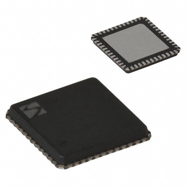
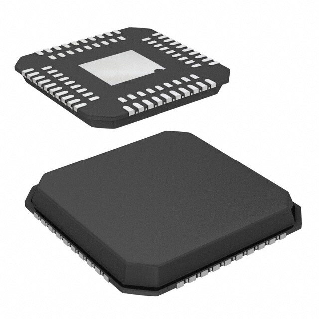
| 产品图片 |
|
| 产品型号 | XE1203FI063TRLF |
| PCN组件/产地 | |
| rohs | 无铅 / 符合限制有害物质指令(RoHS)规范要求 |
| 产品系列 | TrueRF™ |
| 产品目录页面 | |
| 其它名称 | XE1203FI063CT |
| 功率-输出 | 0 ~ 15dBm |
| 包装 | 剪切带 (CT) |
| 天线连接器 | PCB,表面贴装 |
| 存储容量 | - |
| 封装/外壳 | 48-VQFN |
| 工作温度 | -40°C ~ 85°C |
| 应用 | AMR,ISM,家庭自动化,程序控制 |
| 数据接口 | PCB,表面贴装 |
| 数据速率(最大值) | 152.3kbps |
| 标准包装 | 1 |
| 灵敏度 | -114dBm |
| 电压-电源 | 2.4 V ~ 3.6 V |
| 电流-传输 | 62mA |
| 电流-接收 | 14mA |
| 调制或协议 | FSK |
| 频率 | 433MHz,868MHz,915MHz |


- 商务部:美国ITC正式对集成电路等产品启动337调查
- 曝三星4nm工艺存在良率问题 高通将骁龙8 Gen1或转产台积电
- 太阳诱电将投资9.5亿元在常州建新厂生产MLCC 预计2023年完工
- 英特尔发布欧洲新工厂建设计划 深化IDM 2.0 战略
- 台积电先进制程称霸业界 有大客户加持明年业绩稳了
- 达到5530亿美元!SIA预计今年全球半导体销售额将创下新高
- 英特尔拟将自动驾驶子公司Mobileye上市 估值或超500亿美元
- 三星加码芯片和SET,合并消费电子和移动部门,撤换高东真等 CEO
- 三星电子宣布重大人事变动 还合并消费电子和移动部门
- 海关总署:前11个月进口集成电路产品价值2.52万亿元 增长14.8%


PDF Datasheet 数据手册内容提取
XE1203F XE1203F 433 MHz / 868 MHz / 915 MHz Low-Power, Integrated UHF Transceiver GENERAL DESCRIPTION KEY PRODUCT FEATURES The XE1203F is a single chip transceiver operating • RF output power: up to +15 dBm in the 433, 868 and 915 MHz license-free ISM • High reception sensitivity: down to –114 dBm (Industry Scientific and Medical) frequency bands. Its (typical) highly integrated architecture allows for minimum • Low power consumption: external components while maintaining design R = 14 mA; T = 62 mA @15 dBm (typical) X X flexibility. All major RF communication parameters • Supply voltage down to 2.4V are programmable and most of them can be • Data rate from 1.2 to 152.3 kbit/s, NRZ coding dynamically set. The XE1203F offers the excellent • Konnex-compatible operation mode advantage of high data rate communication at rates • 11-bit Barker encoder/decoder of up to 152.3 kbit/s, without the need to modify the number or parameters of the external components. • On-chip frequency synthesizer with minimum The XE1203F is optimized for low power frequency resolution of 500 Hz consumption while offering high RF output power and Continuous phase 2-level FSK modulation exceptional receiver sensitivity. The device is suitable Received data pattern recognition for applications which have to satisfy either the • Bit-Synchronizer for incoming data/clock European (ETSI-300-220) or the North American synchronization and recovery (FCC part 15) regulatory standards. TrueRF™ • RSSI (Received Signal Strength Indicator) technology enables a low –cost external component • FEI (Frequency Error Indicator) count (elimination of the SAW filter) whilst still • RoHS green package satisfying ETSI and FCC regulations. APPLICATIONS ORDERING INFORMATION • Automated Meter Reading (AMR) Part number Temperature Package • Home Automation and Access Control range • High-Quality Speech, Music and Data over RF • Applications requiring Konnex-compatibility XE1203FI063TRLF -40 °C to +85 °C MLPQ48 Rev 2 December 2008 www.semtech.com 1
XE1203F Table of Contents 1 Functional Block Diagram..................................................................................................................3 2 Pin description....................................................................................................................................4 3 Electrical Characteristics...................................................................................................................5 3.1 Absolute Maximum Operating Ranges.................................................................................................5 3.2 Specifications........................................................................................................................................5 3.2.1 Operating Range...................................................................................................................................5 3.2.2 Electrical Specifications........................................................................................................................5 4 GENERAL DESCRIPTION...................................................................................................................7 4.1 The Receiver Section............................................................................................................................7 4.1.1 LNA & Receiver modes.........................................................................................................................8 4.1.2 Demodulation chain..............................................................................................................................8 4.1.3 Demodulator..........................................................................................................................................8 4.1.4 Bit synchronizer....................................................................................................................................9 4.1.5 The DATA and DATAIN pins..............................................................................................................10 4.1.6 Pattern recognition block....................................................................................................................10 4.1.7 RSSI....................................................................................................................................................10 4.1.8 Frequency Error Indicator – FEI.........................................................................................................12 4.2 The Transmitter Section......................................................................................................................13 4.2.1 Transmitter..........................................................................................................................................13 4.2.2 Barker encoder/decoder.....................................................................................................................15 4.3 The Frequency Synthesizer................................................................................................................16 4.3.1 Clock Output for external processor...................................................................................................17 5 SERIAL Interface definition AND Principles of operation............................................................18 5.1 Serial Control Interface.......................................................................................................................18 5.2 Configuration and Status registers.....................................................................................................20 5.2.1 The ConfigSwitch Register.................................................................................................................20 5.2.2 RTParam Configuration Register........................................................................................................22 5.2.3 FSParam Configuration Register........................................................................................................23 5.2.4 SWParam Configuration Register - switching parameters.................................................................24 5.2.5 DataOut Status Register.....................................................................................................................25 5.2.6 ADParam Configuration Register.......................................................................................................25 5.2.7 Pattern register...................................................................................................................................27 5.2.8 Test Registers and additional settings................................................................................................28 5.3 Operating Modes................................................................................................................................28 5.3.1 Standard power up sequence for the receiver and transmitter..........................................................28 5.4 Selection of the reference frequency..................................................................................................29 5.5 Clock Output Interface........................................................................................................................30 5.6 Default settings at power-up...............................................................................................................30 6 Application Information....................................................................................................................31 6.1 RECEIVER Matching network............................................................................................................31 6.2 Transmitter matching network............................................................................................................31 6.3 VCO tank.............................................................................................................................................34 6.4 Loop filter of the frequency synthesizer..............................................................................................34 6.5 frequency synthesizer Reference crystal............................................................................................35 7 Revision History................................................................................................................................36 8 Packaging information.....................................................................................................................37 © Semtech 2008 www.semtech.com 2
XE1203F The XE1203F is a single-chip UHF transceiver integrated circuit intended for use as a low cost FSK transceiver to establish a frequency-agile, half-duplex, bi-directional RF link, with NRZ (non-return to zero) data coding. Barker encoder/decoder hardware can be activated to modulate/demodulate the transmitted signal to reduce the effects of fixed-frequency in-band interference. The device is available in a MLPQ48 package and is designed to provide a fully functional multi-channel FSK transceiver. It is intended for applications in the 868 MHz European band and the North American 902-928 MHz ISM band. The single chip transceiver operates down to 2.4V and provides a low power solution for battery-operated and power sensitive applications. The XE1203F is capable of operating data rates up to 152.3 kbit/s, making it ideally suited for applications where high data rates are required. 1 FUNCTIONAL BLOCK DIAGRAM DFDDDP SFSD SP DD DA MP MP SS SA VDVDVD VSVS VS V VD QA IA V VS QAMP IAMP SI RSSI SO FAMP LPF BBAMP LIM CONTROL SCK RFA DATA MATCHING LNA EN FEI NETWORK SWITCH RFB FAMP LPF BBAMP LIM PATTERN PATTERN MATCHING DCLK PHASE LO_BUF IREF DEMOD BITSYNC SHIFTER DATAIN LOGIC CONTROL DATA 11 Bits BARKER DECODER 11 Bits DIVCTL modulator BARKER /n ENCODER Synthesizer MMOD DIVIDER CLKXTAL XE1203 TrueRF™ XE1203 RFOUT CH PUMP MNEATTWCHOIRNKG PA VCO PFD OSCILLATOR /n IREF CLOCK OUT POR TKA TKB LFB XTA XTB CLKOUT TSUPPTMOD(3:0) POR VCO LOOP TANK FILTER XTAL Figure 1: XE1203F Block Diagram © Semtech 2008 www.semtech.com 3
XE1203F 2 PIN DESCRIPTION PIN NAME I/O Description 1 N.C. Not connected 2 N.C. Not connected 3 N.C. Not connected 4 VSSF Ground for the RF analog blocks 5 RFA IN RF input 6 RFB IN RF input 7 VSSP Ground for the RF power amplifier 8 VSSP Ground for the RF power amplifier 9 RFOUT OUT RF output 10 VDDP Power supply for the RF power amplifier 11 Test pin IN Connected to ground 12 VDDF Power supply for the RF analog blocks 13 VSSF Ground for the RF analog blocks 14 TKA IN/OUT VCO tank 15 TKB IN/OUT VCO tank 16 VSSF Ground for the RF analog blocks 17 LFB IN/OUT Loop filter of the PLL 18 VDDD Power supply for the RF digital blocks 19 VSSD Ground for the RF digital blocks 20 Test pin IN Connected to ground 21 Test pin IN Connected to ground 22 N.C. Not connected 23 Test pin IN Connected to ground 24 Test pin IN Connected to ground 25 VSSA Ground for the analog blocks 26 XTA IN/OUT Crystal and input of external clock 27 VSSA Ground for the analog blocks 28 XTB IN/OUT Crystal 29 VDDA Power supply for the analog blocks 30 QAMP Buffered Q output 31 IAMP Buffered I output 32 Test pin IN Connected to ground 33 Test pin IN Connected to ground 34 Test pin IN Connected to ground 35 EN IN 3-wire interface communication enable signal 36 VDD Power supply for the digital blocks 37 SWITCH IN/OUT Receiver or Transmitter mode selection 38 SO OUT Data output of the 3-wires interface 39 SI IN Data input of the 3-wires interface 40 SCK IN Input clock of the 3-wires interface 41 CLKOUT Out Output clock at quartz frequency divided by 4, 8, 16 or 32 42 VSS Ground for the digital blocks 43 DCLK OUT Transmitter or Receiver clock 44 DATA IN/OUT Transmitter input data or Receiver output data 45 DATAIN IN Transmitter input data 46 PATTERN Out Output of the pattern recognition block 47 N.C. Not connected 48 N.C. Not connected © Semtech 2008 www.semtech.com 4
XE1203F 3 ELECTRICAL CHARACTERISTICS 3.1 ABSOLUTE MAXIMUM OPERATING RANGES Stresses above the values listed below in Table 1 may cause permanent device failure. Exposure to absolute maximum ratings for extended periods may affect device reliability. Symbol Description Min. Max. Unit VDDmax Supply voltage -0.4 3.9 V ML Receiver input level -5 dBm Tmax Storage temperature -55 125 °C Table 1: Absolute Maximum Ratings The device is ESD sensitive and should be handled with precaution. 3.2 SPECIFICATIONS 3.2.1 Operating Range Symbol Description Min. Max. Unit VDD Supply voltage 2.4 3.6 V T Temperature -40 85 °C CLop Load capacitance on digital ports - 25 pF Table 2: Operating Range 3.2.2 Electrical Specifications Table 3 below gives the electrical specifications of the transceiver under the following conditions: Supply Voltage VDD = 3.3V, temperature = 25 °C, 2-level FSK without pre-filtering, carrier frequency fc = 915 MHz, frequency deviation Δf = 55 kHz, bit rate BR = 4.8 kbit/s, Base band filter bandwidth BBW = 200 kHz, bit error rate BER = 0.1% (measured at the output of the bit synchronizer), LNA input and RF PA output matched to 50Ω, environment as defined in Section 6, unless otherwise specified. Symbol Description Conditions Min Typ Max Unit IDDSL Supply current in sleep mode - 0.2 1 uA IDDST Supply current in standby mode Quartz oscillator (39 MHz) - 0.85 1.10 mA enabled IDDR Supply current in receiver mode - 14 17 mA IDDT Supply current in transmitter mode RFOP = 5 dBm - 33 40 mA (with optimum load-matching) RFOP = 15 dBm - 62 75 mA RFS RF sensitivity BR = 4.8 kbit/s Mode A (*1) - -114 -111 dBm BR = 4.8 kbit/s Mode B (*1) - -101 -98 dBm BR = 32.7 kbit/s Mode A (*1) - -109 -106 dBm BR = 32.7 kbit/s Mode B (*1) - -96 -93 dBm Δf = 200 kHz, BBW = 600 kHz BR = 152.3 kbit/s Mode A (*1) - -101 -98 dBm BR = 152.3 kbit/s Mode B (*1) - -89 -86 dBm RFSB RF sensitivity with Barker BR = 1154 bit/s Mode A (*1) - -113 -110 dBm Coding/decoding enabled BR = 1154 bit/s Mode B(*1) - -100 -97 dBm FDA Frequency deviation Programmable 1 - 255 kHz CCR Co-channel rejection -13 -10 - dBc © Semtech 2008 www.semtech.com 5
XE1203F Symbol Description Conditions Min Typ Max Unit IIP3 Input intercept point f = f + 1 MHz 1 LO f = f + 1.945 MHz 2 LO Mode A (*1) -36 -33 - dBm Mode B (*1) -21 -18 - dBm BBW Base band filter bandwidth DSB Programmable (*2) - 200 - kHz - 600 - kHz ACR Adjacent channel rejection funw = f + 650 kHz 45 48 - dBc LO Pw= - 108dBm, mode A (*1) BR Bit rate Programmable 1.2 152.3 kbit/s RFOP RF output power Programmable RFOP1 -3 0 - dBm RFOP2 +2 +5 - dBm RFOP3 +7 +10 - dBm RFOP4 +12 +15 - dBm FR Synthesizer frequency range Programmable 433 - 435 MHz Each range with its own 868 - 870 MHz external components 902 - 928 MHz TS_TR Transmitter wake-up time From oscillator enabled - 150 250 us TS_RE Receiver Baseband wake-up time From oscillator enabled - 0.5 0.8 ms TS_RSSI RSSI wake-up time From receiver enabled - - 1 ms TS_RSSIM RSSI measurement time 0.5 ms TS_OS Crystal oscillator wake-up time Fundamental - 0.3 0.5 ms 3rd overtone - 2.5 ms TS_FEI FEI wake-up time - - 2/BR ms TS_SYNC_AQ Time for synchronization of the Input power of –106 dBm - 5 - ms Barker decoder Data rate = 1154 bits/s Chip rate = 12.7 kcps From Rx enabled XTAL Crystal oscillator frequency Fundamental or 3rd overtone - 39 - MHz FSTEP Frequency synthesizer step Exact step is XTAL / 77 824 - 500 - Hz VTHR RSSI equivalent input thresholds Mode A (*1) Low range:VTHR1 - -100 - dBm VTHR2 - -95 - dBm VTHR3 - -90 - dBm High range:VTHR1 - -85 - dBm VTHR2 - -80 - dBm VTHR3 - -75 - dBm SPR Spurious emissions in Rx mode (*4) - -65 - dBm SCK Serial Clock frequency 1 MHz VIH Digital input level high (*3) % VDD 75 - - % VIL Digital input level low (*3) % VDD - - 25 % VOH Digital output level high % VDD 75 - - % VOL Digital output level low % VDD - - 25 % Table 3: Electrical Specifications Notes: (*1) Mode A: High sensitivity mode; Mode B: High Linearity mode. As defined in Paragraph 4.1.1. (*2) An intermediate bandwidth of 300 kHz can also be selected by using additional settings described in section 5.2.8. (*3) Throughout this document, digital signal levels are named “high” or “1”, and “low” or “0”. (*4) SPR strongly depends on the design of the application board and the choice of the external components. Values down to -70 dBm can be achieved with careful design. © Semtech 2008 www.semtech.com 6
XE1203F 4 GENERAL DESCRIPTION The XE1203F is a direct conversion (Zero-IF) half-duplex data transceiver. The circuit operates in three different ISM frequency bands (433 MHz, 868 MHz and 915 MHz) and uses 2-level FSK modulation/demodulation to provide a complete transmission link. It is capable of operating at data rates between 1.2 and 152.3 kbit/s, making it ideally suited for applications where high data rates are required. It also supports the Konnex standard where the bit rate is 32.7 kbit/s. The device includes dedicated Barker encoder/decoder hardware that may be activated to modulate/demodulate the transmitted signal to reduce in-band interferences. The XE1203F is a highly programmable device – channel, bit rate, frequency deviation, output power, base band filter bandwidth, sensitivity vs. linearity, RSSI feature, and many other parameters – which makes it extremely flexible, to meet a large number of end user requirements. The main functional blocks of the XE1203F are the receiver, the transmitter, the frequency synthesizer and some service blocks. The device also includes a series of configuration and status registers. In a typical application, the XE1203F is programmed by a microcontroller via the 3-wire serial bus SI, SO, SCK to write to and read from these registers. The Receiver converts the incoming 2-level FSK modulated signal into a synchronized bit stream. The Transmitter performs the modulation of the carrier by an input bit stream and the transmission of the modulated signal. The Frequency Synthesizer generates the local oscillator (LO) signal for the receiver section as well as the continuous phase FSK modulated signal for the transmitter section. The Service Blocks provide the internal voltage and current sources and provide all the necessary functions for the circuit to work properly. The Configuration Registers are a set of variable-length registers that are used to store various settings to operate the XE1203F transceiver circuit. They are listed below in Table 4. Refer to Section 5.2 for the detailed descriptions of these registers. These registers are accessed in write or read mode through the 3-wire serial bus, as described in Section 5.1. Name Description ConfigSwitch 1-bit data to switch between 2 sets of user-predefined SWParam Configuration Registers RTParam Receiver and transmitter parameters FSParam LO, Bitrate, Deviation and other frequency parameters SWParam 2 sets of user-predefined configuration registers DataOut Status register which can be read through the 3-wire serial interface ADParam Additional parameters Pattern Reference pattern for the “pattern recognition” feature Table 4: Configuration Registers Naming convention: throughout this document, each individual bit in a particular Configuration Register includes the name of this register followed by a bit identifier. For example, RTParam_Band are the “Band” bits within the RTParam register. The Digital Interface provides internal control signals for the whole circuit according to the configuration register settings. 4.1 THE RECEIVER SECTION The receiver converts the incoming 2-level FSK modulated signal into a synchronized bit stream. The receiver is composed of a low-noise amplifier, two down-conversion mixers, two base band filters, two base band amplifiers, two limiters, a demodulator and a bit synchronizer. The bit synchronizer translates the output of the demodulator into a glitch-free bit stream available on the pin DATA. It also generates a synchronized clock, DCLK, which can be © Semtech 2008 www.semtech.com 7
XE1203F used to sample the DATA signal without additional external signal processing. In addition, the receiver includes a digital Received Signal Strength Indicator (RSSI), a Frequency Error Indicator (FEI) that provides information about the local oscillator frequency error, and a pattern recognition function to detect preprogrammed sequences in the received serial data stream. Finally, a user-selectable Barker coding/decoding feature can be activated to spread the outgoing data with an 11-bit Barker code upon transmission and decode the incoming data upon reception by correlating the spread data with the 11-bit Barker code. 4.1.1 LNA & Receiver modes The LNA of the receiver has two programmable operation modes: the high sensitivity mode, Mode A, for reception of weak signals; and the high linearity mode, Modxe B, for strong signals. The operation mode is defined by the contents of the SWParam_Rmode1 and SWParam_Rmode2 Configuration Register bits. • Mode A: High sensitivity mode, approximately 13dB better than in Mode B (see 3.2.2, RFS parameter) • Mode B: High Linearity mode, IIP3 approximately 15dB higher than in Mode A (see 3.2.2, IIP3 parameter) 4.1.2 Demodulation chain The demodulation chain consists of an FSK demodulator, bit synchronizer, Barker decoder and a Pattern Recognition block. Figure 2 below illustrates the interaction between each section of the demodulation chain. RTParam_Barker pow BARKER DECODER data dclk FSK DATA DEMODULATOR CONTROL data data dclk RTParam_Bitsync pow BIT SYNCHRONIZER data FSParam_BR dclk RTParam_Pattern pow PATTERN pattern RECOGNIZER ADParam_Pattern ADParam_Psize ADParam_Ptol Figure 2: Demodulation architecture 4.1.3 Demodulator The demodulator provides a demodulated data stream from the received FSK modulated base band limited signals, I_lim and Q_lim. If the end-user application requires direct access to the output of the demodulator, then the RTParam_Bitsync and RTParam_Barker Configuration Register bits are set low (disabled). In this case the © Semtech 2008 www.semtech.com 8
XE1203F demodulator output is directly connected to the DATA pin and the DCLK pin is set to low. Otherwise, the demodulator output is processed by the bit synchronizer. For correct operation of the demodulator the modulation index β of the input signal should meet the following condition: 2⋅Δf β= ≥ 2, BR where Δf is the frequency deviation and BR the bit rate. 4.1.4 Bit synchronizer The raw output signal from the demodulator usually contains jitter and glitches. The bit synchronizer transforms the data output of the demodulator into a glitch-free bit stream available on the DATA pin and generates a synchronized clock DCLK to be used for sampling the DATA output (see Figure 3, below). DATA (NRZ) DCLK Figure 3: Bit synchronizer timing diagram. For proper operation, in addition to the requirement for the modulation index defined in 4.1.3 above, the Bit Synchronizer must first receive three bytes of alternating logic value preamble, i.e. “0101” sequences. After this startup phase, the rising edge of DCLK signal is centered on the demodulated bit. Subsequent data transitions will preserve this centering. This has two implications: • If the Bit Rates of Transmitter and Receiver are known to be the same, the XE1203F will be able to receive an infinite unbalanced sequence (all “0s” or all ”1s”) with no restriction. • If there is a difference in Bit Rate between Tx and Rx, the amount of adjacent bits at the same level that the BitSync can withstand can be estimated as: BR Number of Bits = 0.5⋅ ΔBR This implies approximately 6 consecutive unbalanced bytes when the Bit Rate precision is 1%, which is easily achievable (crystal tolerance is in the range of 50 to 100 ppm). It is recommended that the bit rate accuracy be better than ±5% (3% for Konnex mode operation). The bit synchronizer is enabled when RTParam_Bsync Configuration Register bit is high. If this bit set low, the bit synchronizer is disabled. In this case the output of the demodulator is directed to the DATA pin and the DCLK output is set to “0”. The received bit rate is defined by the value of the FSParam_BR Configuration Register, and is calculated as follows: 152.34e3 Bit rate = int(FSParam_BR(6:0)) + 1 where int(x) is the integer value of the unsigned binary representation of (x). Note: for Konnex standard operations, the bit rate is fixed at 32.7 kbit/s. ADParam_enable_konnex should be set to a ‘1’. © Semtech 2008 www.semtech.com 9
XE1203F 4.1.5 The DATA and DATAIN pins The pin DATA is by default used by both the transmitter and the receiver sections. By default it is set as a bidirectional I/O pin. When in receive mode, demodulated data appears at DATA as an output signal. In transmit mode, the transmitted bit stream is applied to this pin as an input. Some applications may require separate input and output pins for the transmitted and received data. In this case the user has to set the ADParam_disable_data_bidir Configuration Register bit to ‘1’. As a result the DATA pin is set as an output only for the received data, while the transmit data is controlled via the DATAIN input pin. 4.1.6 Pattern recognition block When in receiver mode, this feature is activated by setting RTParam_Pattern Configuration Register bit high. The demodulated data signal is compared with a pattern stored in the PATParam_Pattern Configuration Register. The PATTERN output pin is driven by the output of this comparator and is synchronized by DCLK. It is set to high when a matching condition is detected, otherwise set to low. The PATTERN output is updated at the rising edge of DCLK. The number of bits used for comparison is defined in the ADParam_Psize Configuration Register and the number of tolerated errors for the pattern recognition is defined in the ADParam_Ptol register. Figure 4, below, illustrates the pattern matching process. Figure 4: Pattern Matching Operation. 4.1.7 RSSI When enabled, this function provides a Received Signal Strength Indication based on the signal at the output of the base-band filter. To enable the RSSI function, the RTParam_RSSI Configuration Register bit should be set to “1”. When enabled, the status of the RSSI in the DataOut_RSSI register is a 2-bit word which can be read via the serial control interface. The content of the register is defined in Table 5, below, where V is the differential amplitude RFFIL equivalent to the RF input signal with the receiver operated in A-mode. The thresholds, V are the equivalent of TH the signal at the output of the base-band filter stage, divided by the signal gain. DataOut_RSSI Description 0 0 V ≤ VTHR1 RFFIL 0 1 VTHR1 < V ≤ VTHR2 RFFIL 1 0 VTHR2 < V ≤ VTHR3 RFFIL 1 1 VTHR3 < V RFFIL Table 5 RSSI status description Two possible ranges, each having a set of three V threshold values, VTHR1, VTHR2, and VTHR3 (see 3.2.2 for TH actual values), are selected with the RTParam_RSSIR Configuration Register bit. They provide an overall RSSI range of typically 25 dB. The timing diagram of an RSSI measurement is illustrated in the Figure 5 below. When the RSSI function has been activated, the signal strength is periodically measured and the result is stored in the register DataOut_RSSI each time this DataOut_RSSI register is read via the 3-wire serial interface. Note that TS_RS is the wake-up time required after the function has been enabled to ensure that a valid reading of RSSI is obtained. © Semtech 2008 www.semtech.com 10
XE1203F RTParam_Rssi /en TS_RSSI TS_RSSIM rssi_out xxx val1 val2 val3 val4 val5 0 saout_rssi dataout_rssi xxx val1 val4 Figure 5: RSSI measurement timing diagram Note on the Dataout_RSSI update: during a read sequence of the Dataout_RSSI Status Register, the Saout_rssi signal is generated internally as illustrated in the Figure 6 below. It can be seen the value of the Dataout_RSSI Status Register is updated upon transmission of the bit A0 on the SI line. The maximum frequency of SCK during the read operation of the RSSI value is 100 kHz. A(4) A(3) A(2) A(1) A(0) SI EN SO HZ D(7) D(6) D(5) D(4) D(3) D(2) D(1) D(0) HZ SCK saout_rssi Figure 6: Generation of saout_rssi © Semtech 2008 www.semtech.com 11
XE1203F 4.1.8 Frequency Error Indicator – FEI When enabled this function provides an indication of the frequency error of the local oscillator compared with the received carrier frequency. For guaranteed operation of the FEI function the following two conditions should be met: 1) The modulation index, β, should meet the following condition: 2⋅Δf β= ≥ 2, BR where: Δf = frequency deviation of the modulated input signal, BR = input data bit-rate. 2) The bandwidth of the baseband filter (BBW) must be greater than the sum of the frequency offset and the received peak signal bandwidth, as defined below: BBW > f + BW OFFSET SIGNAL where BBW is the baseband filter bandwidth defined by the RTParam_BW register. f is the difference OFFSET ⎛BR ⎞ between the carrier frequency and the LO frequency, and BW is equal to ⎜ +Δf ⎟. SIGNAL ⎝ 2 ⎠ Note on the timing for FEI measurement: The timing diagram of the FEI measurement process is illustrated in Figure 7 below. As long as the FEI function remains enabled, the frequency error is continuously measured every 2/BR seconds, starting TS_FEI (see Paragraph 3.2.2) after the FEI function is enabled. The measurement results are loaded into the status registers Dataout_MSB_fei and Dataout_LSB_fei each time the Dataout_LSB_fei register is read through the 3-wire serial interface. In the diagram below, Saout_fei is generated internally during a read sequence from the “Dataout_LSB_fei ‘’ status register. RTParam_FEI EN TS_FEI 2/BR first fei_out val0 val1 val2 val3 val4 0 evaluation saout_fei Dataout_MSB_fei& xxx val1 val3 Dataout_LSB_fei Figure 7: Timing diagram of the FEI measurement process The maximum frequency of SCK during the FEI read operation is 100 kHz. When using the Konnex standard, the bit ADParam_enable_konnex Configuration Register must be set to ‘1’. © Semtech 2008 www.semtech.com 12
XE1203F The frequency error can then be calculated by using the following formula: Frequency error = (BR/8)*int(Dataout_FEI(11:0)), where Dataout_FEI(11:0) = Dataout_MSB_fei(3:0) + Dataout_LSB_fei(7:0), and int(x) is the integer value of the signed binary representation of x. 4.2 THE TRANSMITTER SECTION The Transmitter performs the modulation of the carrier by an input bit stream and the transmission of the modulated signal. Carrier modulation is achieved directly through the frequency synthesizer via a Sigma-Delta modulator. The frequency deviation and the bit-rate of the modulated carrier are programmable. An on-chip power amplifier then amplifies the RF signal. The output power can be programmed with 4 possible settings: RTParam_Tpow Output power 0 0 RFOP1 0 1 RFOP2 1 0 RFOP3 1 1 RFOP4 Table 6: Output power settings 4.2.1 Transmitter The transmit data should be applied to DATA or DATAIN pins depending on the setting of the ADParam_disable_data_bidir configuration bit. If the parameter is set to “1”, then the DATAIN pin is used, otherwise the bidirectional pin DATA is used. The modulating signal on DATA or DATAIN can be pre-processed before modulating the local oscillator to produce the outgoing FSK RF signal. This is the pre-filtering feature. The pre-filtering is selected by setting the RTParam_Filter configuration bit to “1”. When RTParam_Filter is set to “1”, the input baseband data is pre-filtered before being applied to the frequency synthesizer. This means that the rising and falling edge of each bit is linearly smoothed with a staircase transition. When RTParam_Filter is set to “0”, the input baseband data is applied directly to the frequency synthesizer without any pre-filtering function. The two possible modulation methods are shown in Figure 8, where “datain” is the input bit stream from DATA or DATAIN pins. © Semtech 2008 www.semtech.com 13
XE1203F Datain or data No filtering IN freq_synth Staircase filtering IN freq_synth Figure 8: Modulation with and without pre-filtering The main characteristic of this pre-filtering function is the ratio between the rise/fall time to the bit duration, t /t . rise bit The value of this ratio can be programmed between two pre-defined values in the RTParam_Stair configuration bit, as shown in the Table 7. RTParam_Stair t /t rise bit 0 10% 1 20% Table 7: t /t ratio rise bit When the pre-filtering function is enabled (RTParam_Filter set to “1”), only the following bit rates and frequency deviations can be used: FSParam_Dev Frequency deviation 00101000 40 kHz 00110111 55 kHz 01010000 80 kHz 10100000 160 kHz 11001000 200 kHz © Semtech 2008 www.semtech.com 14
XE1203F FSParam_Br Bit rate (bit/s) 1111110 1200 0111111 2400 0011111 4800 0001111 9600 0000111 19200 0000011 38400 0000001 76800 others (*) 153000 Table 8: Possible bit rates and frequency deviations when pre-filtering is enabled (*) For any programmed value of FSParam_Br which is not in the Table 8 above, the data-rate is fixed to 153 kbit/s and the pre-filtering is applied as defined by the user. If ADParam_enable_konex is set high, then the pre-filtering option is available for a bit rate of 32.7 kbit/s and one of the frequency deviations defined above. 4.2.2 Barker encoder/decoder The Barker encoder/decoder hardware can be activated to modulate/demodulate the transmitted signal to reduce in-band interferences The Barker decoder provides an alternative to the bit synchronizer only for a fixed data rate of 1154bits/s. The Barker block is selected when the RTParam_Barker configuration bit is set to “1”. In transmission, the information data at a bit rate of 1154bits/s is spread using an 11-bit Barker code. The result is an encoded bit stream at 12.7 kilochips per second (kcps), which is applied to the frequency synthesizer. On the receiver part, the signal is demodulated using the FSK demodulator (at 12.7 kcps) and then fed into the Barker decoder to recover the un-encoded data at 1154 bit/s, together with a synchronized clock to sample it. Figure 8 on the next page, illustrates the coding/decoding process. Figure 9: Barker Encoding and Decoding Channels. In receiver mode, the XE1203F provides a clock output, DCLK, to a microcontroller. The data can be sampled at the rising edge of the clock. When using the Barker decoding process, DCLK is used to detect the sync acquisition. If there is no valid data, DCLK remains high. The first falling edge of the clock means that the sync acquisition phase has been reached and that the output data is now available. This is illustrated below in Figure 10. © Semtech 2008 www.semtech.com 15
XE1203F Figure 10: Data exchange during reception mode with Barker the feature enabled When using the Barker encoding in transmitter mode, the RTParam_Barker parameter is set to “1” and the baseband data at 1154 bit/s is applied through either the DATA or DATAIN depending to the status of ADParam_disable_data_bidir. The data is spread into an encoded chip stream at 12.7 kcps by the Barker encoder. This chip stream is directly applied to the frequency synthesizer without any pre-filtering. When using the Barker coder/decoder feature in transmission mode, the DCLK pin is used to synchronize the data coming from a microcontroller or another source. This DCLK clock is generated by the XE1203F. At the falling edge of the each clock a new data bit (on DATA or DATAIN) should be supplied by the microcontroller or another source. This data is sampled by the XE1203F at the next rising edge of DCLK. It is then spread by using an 11-bit length Barker code. The Figure 11 shows the data exchange during the transmission mode when the Barker feature is enabled. dclk @1154 Hz information data from a microcontroller bit0 bit1 bit2 bit3 bit4 bit5 bit6 bit rate = 1154 bps Spread data @12.7 Kchps spread spread spread spread spread spread bit0 bit1 bit2 bit3 bit4 bit5 Figure 11: Data exchange during transmission mode with the Barker feature enabled 4.3 THE FREQUENCY SYNTHESIZER © Semtech 2008 www.semtech.com 16
XE1203F The Frequency Synthesizer generates the local oscillator (LO) signal for the receiver section as well as the continuous phase FSK (CPFSK) modulated signal for the transmitter section. The core of the synthesizer is implemented with a Sigma-Delta PLL architecture. The frequency is programmable with a minimum step-size of 500 Hz in the 433, 868 and 915 MHz frequency bands. This block includes a crystal oscillator which provides the frequency reference for the PLL. This reference frequency can also be used as a reference clock for the external microcontroller on the CLKOUT pin. 4.3.1 Clock Output for external processor A reference clock can be generated by XE1203F for use by an external microcontroller. The RTParam_Clkout configuration bit determines the status of the CLKOUT pin. When set high CLKOUT is enabled, otherwise it’s disabled. The output frequency at CLKOUT is defined by the value of the ADParam_Clkfreq parameter. The output frequency at CLKOUT is the reference oscillator frequency divided by 4, 8, 16 or 32. With the reference oscillator frequency at 39 MHz this provides a reference clock at 9.75 MHz, 4.87 MHz, 2.44 MHz or 1.22 MHz, respectively. This clock signal is disabled in Sleep Mode. © Semtech 2008 www.semtech.com 17
XE1203F 5 SERIAL INTERFACE DEFINITION AND PRINCIPLES OF OPERATION 5.1 SERIAL CONTROL INTERFACE A 3-wire bi-directional bus (SCK, SI, SO) is used to communicate with the XE1203F. SCK and SI are input signals supplied externally, for example by the microcontroller. The XE1203F configures the SO signal as an output pin during read operation, and it is tri-stated in other modes. The falling edge of the SCK signal is used to sample the SI pin to write data into the internal shift register of the XE1203F. The rising edge of the SCK signal is used to output data to SO pin by XE1203F, so the microcontroller should sample data at the falling edge of SCK. The signal EN must be low during the whole write and read sequences. In write mode the content of the particular configuration register (see 5.2) is updated on the next rising edge of the EN signal. Before this rising edge, the new data is stored in temporary registers which do not affect the transceiver settings. The timing diagram of a write sequence is illustrated in Figure 12 below. The sequence is initiated when a Start condition is detected, defined by the SI signal being set to “0” during one period of SCK. The next bit is a read/write (R/W) bit which should be “0” to indicate a write operation. The next 5 bits contain the address of the configuration/status registers A[4:0] to be accessed, MSB first (see 5.2). Then, the next 8 bits contain the data to be written into the register. The sequence ends with 2 stop bits set to “1”. The data on SI should change on the rising edges of SCK, and is sampled on the falling edge of SCK. After the 2 stop bits, the data transfer is terminated. The SI line should be at “1” for at least one extra SCK clock cycle before a new write or read sequence can start. This mode of operation allows data to be written into multiple registers keeping the EN line low. The maximum frequency of SCK is 1 MHz, except as defined above when reading the RSSI or FEI outputs, where the maximum frequency of SCK is limited to 100 kHz. The minimum clock pulse width is 0.5 us. Over the operating supply and temperature range, set-up and hold time for SI on the falling edge of SCK are 200 ns. The register at address 0 is one bit long. When writing this register, the sequence described above is valid except that only one data bit is required instead of 8. However, if a single write procedure is used for all registers 8 data bits must be sent when writing at address 0, but only the MSB will be stored at address 0. The remaining 7 data bits must all be “1”. sck A(4) A(3) A(2) A(1) A(0) D(7) D(6) D(5) D(4) D(3) D(2) D(1) D(0) si /en so High impedance Figure 12: Write sequence into configuration register Figure 13 illustrates a write sequence at address zero. © Semtech 2008 www.semtech.com 18
XE1203F sck si A(4) A(3) A(2) A(1) A(0) D(7) /en so High impedance Figure 13: Write sequence into configuration register at address zero The time diagram of a read sequence is illustrated in Figure 14 below. The sequence is initiated when a Start condition is detected, defined by the SI signal being set to “0” during a period of SCK. The next bit is a read/write (R/W) bit which should be “1” to indicate a read operation. The next 5 bits are the address of the control register A[4:0] to be accessed, MSB first. The data from the register is then output on the SO pin. The data become valid at the rising edges of SCK and should be sampled at the falling edge of SCK. After this, the data transfer is terminated. The SI line must stay high for at least one extra SCK clock cycle to start a new write or read sequence. The maximum current drive on SO is 2 mA at a supply voltage of 2.7V and the maximum load is CLop, as defined in Paragraph 3.2.2. When the serial interface is not used for read or write operations, both SCK and SI should be set to “1”. Except when in read mode, SO is set to a high impedance mode. sck A(4) A(3) A(2) A(1) A(0) si /en so High impedance D(7) D(6) D(5) D(4) D(3) D(2) D(1) D(0) High impedance Figure 14: Read sequence of configuration register When reading the register at address zero, the timing diagram is illustrated in Figure 15. © Semtech 2008 www.semtech.com 19
XE1203F sck si A(4) A(3) A(2) A(1) A(0) /en so High impedance D(7) High impedance Figure 15: Read sequence of configuration register at address 0 5.2 CONFIGURATION AND STATUS REGISTERS The XE1203F has several operating modes and configuration parameters which can be programmed by the user or the application. In addition, status information may be read from the circuit. Some of the operating modes, the status information and the configuration parameters are stored in a series of internal Configuration and Status Registers that can be accessed by the microcontroller through the 3-wire serial interface. There are seven variable Configuration and Status Registers, as listed below in Table 9. Name Description Size Address (bits) (binary format) ConfigSwitch 1-bit data to switch between 2 sets of 1 x 1 00000 user-predefined SWParam Configuration Registers RTParam Receiver and transmitter parameters 2 x 8 00001 - 00010 FSParam LO, Bitrate, Deviation and other 3 x 8 00011 - 00101 frequency parameters SWParam 2 sets of user-predefined configuration 6 x 8 00110 - 01011 registers DataOut Status register which can be read 2 x 8 01100 - 01101 through the 3-wire serial interface ADParam Additional parameters 5 x 8 01110 - 10010 Pattern Reference pattern for the “pattern 4 x 8 10011 - 10110 recognition” feature Table 9: Configuration and Status Registers List All the bits that are referred to as “reserved” in this section should be set to “0” during write operations. 5.2.1 The ConfigSwitch Register When operating the XE1203F, it might by useful to quickly switch between two pre-defined operating modes, to save time and traffic on the 3-wire serial interface bus. This may occur when the XE1203F is required to switch quickly between receive and transmit mode, when it has to operate on two different carrier frequencies, or when it has to switch between the high linearity mode B and the high sensitivity mode A. For that purpose, the five parameters stored in the SWParam Configuration Register are duplicated: the configuration set#1 and the configuration set #2. © Semtech 2008 www.semtech.com 20
XE1203F Depending on the ConfigSwitch 1-bit Register or the input level at the SWITCH pin, the XE1203F transceiver will use either the SWParam configuration set#1 or the set #2. If the RTParam_Switch_ext configuration parameter is low, then the SWParam configuration set is selected by the ConfigSwitch parameter – set#1 if ConfigSwitch is “0”, set#2 if ConfigSwitch is “1”. If the RTParam_Switch_ext configuration parameter is high, then the SWParam configuration set is selected by the SWITCH pin – set#1 if SWITCH is low, set#2 if SWITCH is high. Table 10 below summarizes the chip configuration programming: ConfigSwitch SWITCH pin RTParam_switch_ext SWParam configuration Register configuration parameter set selected 0 SWITCH is an output: 0 Set #1: ‘1’ in transmitter mode SWParam_mode_1 ‘0’ in the other modes SWParam_Power_1 SWParam_Rmode_1 SWParam_t_delsig_in_1 SWParam_freq_1 1 SWITCH is an output: 0 Set #2: ‘1’ in transmitter mode SWParam_mode_2 ‘0’ in the other modes SWParam_Power_2 SWParam_Rmode_2 SWParam_t_delsig_in_2 SWParam_freq_2 X 0 1 Set #1: SWParam_mode_1 SWParam_Power_1 SWParam_Rmode_1 SWParam_t_delsig_in_1 SWParam_freq_1 X 1 1 Set #2: SWParam_mode_2 SWParam_Power_2 SWParam_Rmode_2 SWParam_t_delsig_in_2 SWParam_freq_2 Table 10: ConfigSwitch, SWITCH pin and SWParam Configuration Register By default the configuration set#1 is used and register RTParam_switch_ext is set to ‘0’. Note that a new value of the ConfigSwitch register or at the SWITCH pin should be modified when the EN signal is low. The actual switch to the newly selected set of SWParam register will be applied to the transceiver on the next rising edge of the EN signal. © Semtech 2008 www.semtech.com 21
XE1203F 5.2.2 RTParam Configuration Register Receiver and transmitter parameters Name Bits Address Description RTParam_Bitsync 7 00001 Bit synchronizer 0 -> disabled 1 -> enabled RTParam_Barker 6 00001 BARKER coder/decoder: 0 -> disabled 1 -> enabled RTParam_Rssi 5 00001 RSSI function: 0 -> disabled 1 -> enabled RTParam_Rssir 4 00001 RSSI range: 0 -> low range (see 3.2.2) 1 -> high range (see 3.2.2) RTParam_Fei 3 00001 FEI function: 0 -> disabled 1-> enabled RTParam_BW 2 00001 Baseband filter bandwidth (BBW) 0 -> 200 kHz (DSB) 1 -> 600 kHz (DSB) RTParam_Osc 1 00001 Reference frequency source: 0 -> internal crystal oscillator 1 -> external source RTParam_Clkout 0 00001 CLKOUT - Reference frequency divided by 4,8,16,or 32: 0 -> disabled 1 -> enabled RTParam_Stair 7 00010 Transmitter pre-filter rise/fall time: 0 -> 10% of bit duration 1 -> 20% of bit duration RTParam_Filter 6 00010 Pre-filtering of the bit stream in transmitter mode 0 -> no filtering 1 -> filtering The filtering function is available only for the following bit rates and frequency deviations: FSPanam_Br = "1111110" -> BR = 1200 bit/s FSPanam_Br = "0111111" -> BR = 2400 bit/s FSPanam_Br = "0011111" -> BR = 4800 bit/s FSPanam_Br = "0001111" -> BR = 9600 bit/s FSPanam_Br = "0000111" -> BR = 19200 bit/s FSPanam_Br = "0000011" -> BR = 38400 bit/s FSPanam_Br = "0000001" -> BR = 76800 bit/s FSParam_Dev = "00101000" -> Δf = 40 kHz FSParam_Dev = "00110111" -> Δf = 55 kHz FSParam_Dev = "01010000" -> Δf = 80 kHz FSParam_Dev = "10100000" -> Δf = 160 kHz FSParam_Dev = "11001000" -> Δf = 200 kHz RTParam_Modul 5 00010 Transmitter modulation: 0 -> enabled 1 -> disabled © Semtech 2008 www.semtech.com 22
XE1203F Name Bits Address Description RTParam_IQAMP 4 00010 I&Q amplifiers: 0 -> disabled 1 -> enabled RTParam_Switch_ext 3 00010 SWParam configuration set selection: 0 -> configuration set defined by ConfigSwitch. SWITCH is an output 1 -> configuration set defined by the pin SWITCH. SWITCH is an input RTParam_Pattern 2 00010 Pattern recognition function: 0 -> disabled 1 -> enabled RTParam_Band 1-0 00010 Frequency band: 01 -> 433 – 435 MHz 10 -> 868 – 870 MHz 11 -> 902 – 928 MHz Table 11: RTParam Configuration Register 5.2.3 FSParam Configuration Register LO, Bitrate, Deviation and other frequency parameters Name Bits Address Description FSParam_Dev 7-0 00011 Frequency deviation Δf: Δf =int( FSParan_Dev) * 1 kHz, where int(x) = integer value of the binary representation of x. Example: 00000001 -> Δf = 1 kHz 11111111 -> Δf = 255 kHz FSParam_Change_Osr 7 00100 OSR Mode (Oversampling Rate mode): 0 -> default Bit rate defined by FSParam_Br 1 -> variable OSR FSParam_Br 6-0 00100 Bit rate (when "FSParam_Change_Osr” = “0”): Br = 152340/(int(FSParam_Br)+1), where int(x) = integer value of the binary representation of x. Example: 0000000 -> Br = 152.34 kbit/s 1111111 -> Br = 1.19 kbit/s 0000100 -> Br = 32.7 kbit/s used in Konnex mode FSParam_OSR 7-0 00101 Define BR in terms of FSParam_BR and FS_Param_OSR: FSParam_OSR = “00011101” and FSParam_Change_Osr = ‘1’ for Konnex standard Table 12: FSParam Configuration Register © Semtech 2008 www.semtech.com 23
XE1203F 5.2.4 SWParam Configuration Register - switching parameters The table below shows 2 sets of user-predefined configuration registers. Please refer to Section 5.2 for more details. Name Bits Address Description SWParam_mode_1 7-6 00110 Chip mode configuration set#1: 00 -> Sleep mode 01 -> Stand by mode 10 -> Receiver mode 11 -> Transmitter mode SWParam_Power_1 5-4 00110 Transmitter output power configuration set#1: 00 -> 0 dBm 01 -> 5 dBm 10 -> 10 dBm 11 -> 15 dBm SWParam_Rmode_1 3 00110 Receiver Mode configuration set#1: 0 -> Mode A (high sensitivity) 1 -> Mode B (high linearity) RESERVED 2-0 00110 RESERVED SWParam_Freq_1 7-0 00111 LO frequency in 2’s complement representation configuration set#1: 7-0 01000 00…0 -> Flo = middle of the range 0X…X-> Flo = higher than the middle of the range 1X…X-> Flo = lower than the middle of the range see Table 14 below SWParam_node_2 7-6 01001 Chip mode configuration set#2: 00 -> Sleep mode 01 -> Stand by mode 10 -> RX mode 11 -> TX mode SWParam_Power_2 5-4 01001 Transmitter output power configuration set#2: 00 -> 0 dBm 01 -> 5 dBm 10 -> 10 dBm 11 -> 15 dBm SWParam_Rmode_2 3 010001 Receiver Mode configuration set#2: 0 -> Mode A (high sensitivity) 1 -> Mode B (high linearity) RESERVED 2-0 01001 RESERVED SWParam_Freq_2 7-0 01010 LO frequency in 2’s complement representation configuration set#2: 7-0 01011 00…0 -> Flo = middle of the range 0X…X-> Flo = higher than the middle of the range 1X…X-> Flo = lower than the middle of the range see Table 14 below Table 13: SWParam Configuration Register The table following provides examples of LO frequency settings with FSParam_Freq: © Semtech 2008 www.semtech.com 24
XE1203F SWParam_Freq_1 MSB (Byte SWParam_Freq_1 LSB (Byte Resulting LO setting address 00111) address 01000) Note: reference frequency = 39.0 MHz or or SWParam_Freq_2 MSB (Byte SWParam_Freq_1 LSB (Byte address 01010) address 01011) Bit 7 Bit 0 Bit 7 Bit 0 F0, where F0 depends on the selected frequency band (see RTParam_Band ) 00000000 00000000 F0 = 434.0 MHz for the 433-435 MHz band F0 = 869.0 MHz for the 868-870 MHz band F0 = 915.0 MHz for the 902-928 MHz band 00000000 00000001 F0 + 500 Hz 00000000 00000010 F0 + 2 * 500 Hz 11111111 11111111 F0 – 500 Hz 11111111 11111110 F0 – 2 * 500 Hz Table 14: Examples of LO frequency settings 5.2.5 DataOut Status Register Status register which can be read through the 3-wire serial interface Name Bits Address Description DataOut_Rssi 7-6 01100 RSSI output: 0 0 -> lowest level, ≤VTHR1 0 1 -> 2nd level, VTHR1<RSSI level≤VTHR2 1 0 -> 3rd level, VTHR2<RSSI level≤VTHR3 1 1 -> highest level, VTHR3<RSSI level RESERVED 5-4 01100 RESERVED DataOut_MSB_fei 3-0 01100 Fei output (MSB) DataOut_LSB_fei 7-0 01101 Fei output (LSB) Ferror = (Br/8)*int(DataOut_MSB_fei & DataOut_LSB_fei) Where int(x) = integer value of the binary representation of x Table 15: DataOut Status Register 5.2.6 ADParam Configuration Register Additional parameters Name Bit Addres Description s s ADParam_Psize 7-6 01110 Size of reference pattern recognition word: 0 0 -> 8 bits 0 1 -> 16 bits 1 0 -> 24 bits 1 1 -> 32 bits ADParam_Ptol 5-4 01110 Number of tolerated errors for the pattern recognition: 00 -> 0 error 01 -> 1 error 10 -> 2 errors 11 -> 3 errors © Semtech 2008 www.semtech.com 25
XE1203F Name Bit Addres Description s s ADParam_Clk_freq 3-2 01110 CLKOUT frequency (if enabled) 00 -> 1.22 MHz (div ratio :32) 01 -> 2.44 MHz (div ratio :16) 10 -> 4.87 MHz (div ratio :8) 11 -> 9.75 MHz (div ratio :4) ADParam_Invert 1 01110 Inversion of Rx output data: 0 -> disabled 1 -> enabled ADParam_RegBW 0 01110 Baseband filter bandwidth calibration: 0 -> enabled 1 -> disabled ADParam_Regfreq 7 01111 Period of baseband filter bandwidth calibration whilst Rx enabled: 0 -> only at start-up of the receiver 1 -> 60 seconds (default mode) or 7 seconds (test mode) ADParam_Regcond 6 01111 Baseband filter bandwidth calibration as a function of selected bandwidth: 0 -> calibration restarted each time the bandwidth is changed 1 -> no calibration when the bandwidth is changed ADParam_Xsel 5 01111 Selection of the XOSC load capacitance mode: 0 -> CL+C0 = 15 pF 1 -> CL+C0 = 11 pF, low current mode ADParam_Resxosc 4-1 01111 Selection of the value of the shunt resistor across ports TKA and TKB for a third overtone XTAL operation: 0000 -> 3800 kΩ 0001 -> 2.55 kΩ 0010 -> 4.65 kΩ 0011 -> 1.78 kΩ 0100 -> 8.79 kΩ 0101 -> 2.07 kΩ 0110 -> 3.22 kΩ 0111 -> 1.56 kΩ 1000 -> 16.55 kΩ 1001 -> 2.26 kΩ 1010 -> 3.79 kΩ 1011 -> 1.66 kΩ 1100 -> 6.04 kΩ 1101 -> 1.91 kΩ 1110 -> 2.81 kΩ 1111 -> 1.48 kΩ ADParam_enable_konnex 0 01111 Konnex mode: 0 -> disabled 1 -> enabled ADParam_Chge_thres 7 10000 Enable programming of the sync and acquisition thresholds: 0 -> threshold are hard-coded and sync-loss counter is 50 bits 1 -> threshold are defined by BParam_Sync_thres and BParam_Trac_thres Sync loss counter is variable and defined by ADParam_Sync_loss ADParam_Sync_thres 6:0 10000 Barker mode sync acquisition threshold ADParam_disable_data_bidi 7 10001 DATA port bidirectional mode: r 0 -> enabled 1 -> disabled: DATA = output, DATAIN = input ADParam_Trac_thres 6-0 10001 Threshold for tracking Barker mode © Semtech 2008 www.semtech.com 26
XE1203F Name Bit Addres Description s s ADParam_Fix_bsync 7 10010 bit synchronizer configuration: 0-> default configuration 1-> high-interference environment ADParam_Sync_loss 6-0 10010 Number of bits before sync loss detection for Barker decoding algorithm Table 16: ADParam Configuration Register 5.2.7 Pattern register This register holds the user supplied reference pattern of 8, 16, 24, or 32 bits (see the ADParam_Psize parameter). The first byte of this pattern is always stored in the byte at address A[4:0] = 10011. If used, the 2nd byte is stored at address A[4:0] = 10100, the 3rd byte at address A[4:0] = 10101, and finally the 4th byte at address A[4:0] = 01011. The MSB bit of the reference pattern is always bit 7 of address 10011. Comparing the demodulated data, the first bit received of the last word is compared with bit 7 (the MSB) of byte address 10011. The last bit received is compared with bit 0 (the LSB) in the Pattern register. Name Bits Byte Address Description PATParam_Pattern 7-0 10011 1st byte of the reference pattern 10100 2nd byte 10101 3rd byte 10110 4th byte Table 17: PATParam Pattern Registers Example of pattern recognition with a 32-bit pattern: Byte Address Byte Address Byte Address Byte Address 10011 10100 10101 10110 Bit 7 Bit 0 Bit 7 Bit 0 Bit 7 Bit 0 Bit 7 Bit 0 10010011 10101010 10010011 10101010 101 10010011 10101010 10010011 10101010 previous bits from last bit received demodulator Figure 16: Example of pattern recognition with a 32-bit pattern Example of pattern recognition with an 8-bit pattern: Byte Address Byte Address Byte Address Byte Address 10011 10100 10101 10110 Bit 7 Bit 0 Bit 7 Bit 0 Bit 7 Bit 0 Bit 7 Bit 0 10010011 Xxxxxxxx Xxxxxxxx Xxxxxxxx 101 10010011 previous bits from last bit received demodulator Figure 17: Example of pattern recognition with an 8-bit pattern © Semtech 2008 www.semtech.com 27
XE1203F 5.2.8 Test Registers and additional settings Some settings in this 9-byte register can be used to have access to additional configurations of the circuit. These settings are described in the Table 18 below: Name Bits Byte Address Description TParam_BW 3 10111 Baseband filter bandwidth (DSB): 0 -> default values defined by RTParam_BW (200 and 600 kHz) 1 -> 300kHz TParam_HPF 1-0 10111 SSB cut-off frequency of the HPF stage (for cancellation of DC and low-frequency offsets in the baseband circuit): 00 -> 4.3 kHz 01 -> 8.7 kHz 10 -> 17.3 kHz 11 -> 34.6 kHz Table 18: Test registers and additional settings 5.3 OPERATING MODES The XE1203F has four main operating modes illustrated in Table 19 below. These modes are defined by the content of the SWParam_mode_1 parameter when configuration set #1 is selected, or by the content of the SWParam_mode_2 parameter when configuration set #2 is selected. See also Section 5.2.1. Mode SWParam_mode1(1:0) Description SWParam_mode_2(1:0) Sleep mode 0 0 - Standby mode 0 0 Quartz oscillator enabled Receiver mode 1 0 Quartz oscillator, Frequency synthesizer, Receiver enabled Transmitter mode 1 1 Quartz oscillator, Frequency synthesizer, Transmitter enabled Table 19: XE1203F Operating Modes 5.3.1 Standard power up sequence for the receiver and transmitter The XE1203F circuit can be switched between any configuration by using the 3 wire interface (ConfigSwitch) or by using the pad SWITCH. This section describes the switching sequence of the chip. Figure 18 shows the transition sequence from sleep mode to receiver mode via stand by mode. © Semtech 2008 www.semtech.com 28
XE1203F SLEEP -> STAND_BY -> RECEIVER Programmed SLEEP STAND_BY RECEIVER mode EN TS_RE TS_OS Actual mode SLEEP STAND_BY RECEIVER SLEEP -> STAND_BY -> TRANSMITTER Programmed SLEEP STAND_BY TRANSMITTER mode EN TS_TR TS_OS Actual mode SLEEP STAND_BY TRANSMITTER TRANSMITTER -> RECEIVER Programmed TRANSMITTER RECEIVER mode EN TS_RE Actual mode TRANSMITTER RECEIVER RECEIVER -> TRANSMITTER Programmed RECEIVER TRANSMITTER mode EN TS_TR Actual mode RECEIVER TRANSMITTER Figure 18: Mode transition 5.4 SELECTION OF THE REFERENCE FREQUENCY The reference clock used by the frequency synthesizer and internal digital circuit can be generated internally by connecting an external crystal between XTA and XTB, or provided by an external oscillator. When using an external source, the signal should be applied to port XTA and the RTParam_Osc configuration bit should be set to “1”. © Semtech 2008 www.semtech.com 29
XE1203F The XE1203F can be used with a 39 MHz crystal operating in fundamental mode or in 3rd overtone mode. For third overtone operation, an internal resistor to be switched across the crystal terminals XTA and XTB is required. This resistor can be selected by programming the ADParam_Resxosc(3:0) parameter. The required value depends on the overtone crystal specification. When using 3rd overtone mode, the user should be aware that during its power up the XE1203F oscillator will attempt to start at the fundamental frequency of the crystal. It will only switch to the overtone mode when properly programmed through the 3-wire interface bus. As a result, if a microcontroller uses the XE1203F CLKOUT as a clock source it is advisable to allow the oscillator frequency to settle before undertaking any time or timing sensitive operations. For fundamental mode operation, the ADParam_Resxosc(3:0) parameter is set to the default value of ”0000’’. This switches a 3.8 MΩ resistance across the crystal terminals. 5.5 CLOCK OUTPUT INTERFACE When register “RTParam_Clkout” is set to “1” , the reference frequency is divided by 4, 8, 16 or 32, depending on the value of the register “ADParam_Clkfreq”, and provides a reference signal at CLKOUT for a microcontroller or external circuitry. If the reference frequency is 39 MHz, then the output frequency available at CLKOUT is as defined in Table 20 below: ADParam_Clkfreq CLKOUT frequency 00 1.22 MHz 01 2.44 MHz 10 4.87 MHz 11 9.75 MHz Table 20: Clock Output Frequency Selection When the XE1203F is in sleep mode, CLKOUT is disabled even if RTParam_Clkout remains high. 5.6 DEFAULT SETTINGS AT POWER-UP The internally generated power-on-reset signal sets the RTParam, FSParam, ADParam and Pattern registers to the 00hex value. There is one important exception for CLKOUT. Although the RTPAram_CLkout is set to ”0” at power-on reset, meaning the feature should be disabled, the XE1203F will generate a CLKOUT signal after a power-on reset to provide a clock signal to a possible microcontroller connected to it. After a power-on reset, CLKOUT will be the lowest available frequency, e.g. 1.22 MHz with a 39 MHz reference frequency. Then, on the first rising edge of the /EN signal – for example after a programming sequence via the 3-wire interface bus - the content of the configuration registers will be updated. If the RTParam Configuration Register has not been programmed during this first sequence after a power-on reset, the CLKOUT clock signal will be disabled. It is strongly advised to initialize the RTPAram_CLkout parameter appropriately during the first programming sequence after a power-on reset, especially if an external microcontroller does use this CLKOUT clock signal to operate. It is recommended to initialize the XE1203F registers immediately after power-up. © Semtech 2008 www.semtech.com 30
XE1203F 6 APPLICATION INFORMATION This section provides details of the recommended component values for the frequency dependant blocks of the XE1203F. Note that these values are dependent upon circuit layout and PCB structure, and that decoupling components have been omitted for clarity. 6.1 RECEIVER MATCHING NETWORK The schematic of the matching network at the input of the receiver is given below in Figure 19 (for a source impedance of 50Ω). CR1 SOURCE RFA LR1 XE1203 CR3 RFB CR2 Figure 19: Receiver matching network The typical recommended values for the external components are shown in Table 21: Name Typical Value Typical Value Typical Value Tolerance for 434 MHz for 868 MHz for 915 MHz CR1 1.5 pF 1.5 pF 1.0 pF ± 5% CR2 1.5 pF 1.2 pF 1.0 pF ± 5% CR3 NC NC NC ± 5% LR1 100 nH 27 nH 27 nH ± 5 % Table 21: Typical component values for the matching network 6.2 TRANSMITTER MATCHING NETWORK The optimum load impedances for 15 dBm output power at the three main frequencies are shown in Table 22: 434 MHz 868 MHz 915 MHz PA optimum load 102 – 12j 78 + 19j 83 + 18j Table 22: Optimum load impedances for 15 dBm output power The Smith charts in Figure 20, Figure 21, and Figure 22 below show contours of output power versus load impedance when the highest transmit level is selected, i.e. 15 dBm: © Semtech 2008 www.semtech.com 31
XE1203F 434 MHz – 15 dBm 0.8 1 1.2 0.6 1.6 2 0.4 3 0.3 0.2 0.1 0 0.1 0.2 0.3 0.5 1 1.4 15 dBm 14 dBm 0.1 0.2 0.3 12 dBm 3 0.4 2 0.6 1.6 0.8 1 1.2 Figure 20: Output power vs. load impedance at 434 MHz 868 MHz – 15 dBm 0.8 1 1.2 0.6 1.6 2 0.4 3 0.3 0.2 0.1 15 dBm 0 0.1 0.2 0.3 0.5 1 1.4 2 14 dBm 0.1 0.2 12 dBm 0.3 3 0.4 2 0.6 1.6 0.8 1.2 1 Figure 21: Output power vs. load impedance at 868 MHz © Semtech 2008 www.semtech.com 32
XE1203F 915 MHz – 15 dBm 0.8 1 1.2 0.6 1.6 2 0.4 3 0.3 0.2 0.1 15 dBm 0 0.1 0.2 0.3 0.5 1 1.4 2 0.1 14 dBm 0.2 12 dBm 0.3 3 0.4 2 0.6 1.6 0.8 1.2 1 Figure 22: Output power vs. load impedance at 915 MHz The schematic of the recommended matching network at the output of the transmitter is shown in Figure 23 below. The two Π-sections are used to provide harmonic filtering in order to satisfy FCC and ETSI regulations. VDD CT2 1 T L XE1203F CT3 LT3 5 4 LT2 1 T T T C C C Figure 23: Transmitter output network © Semtech 2008 www.semtech.com 33
XE1203F The typical component values of this matching circuit are shown below in Table 23: Name Typical Value Typical Value Typical Value Tolerance for 434 MHz for 868 MHz for 915 MHz CT1 6.8 pF 1.5 pF 1.8 pF ± 5% CT2 1.0 pF 0.56 pF NC ± 5% CT3 22 pF 15 pF 33 pF ± 5% CT4 6.8 pF 3.3 pF 3.3 pF ± 5% CT5 4.7 pF 2.2 pF 2.2 pF ± 5% LT1 33 nH 39 nH 47 nH ± 5% LT2 22 nH 10 nH 10 nH ± 5% LT3 22 nH 8.2 nH 8.2 nH ± 5% Table 23: Typical component values for the recommended matching network at the output of the transmitter 6.3 VCO TANK The tank of the VCO is implemented with one inductor in parallel with one capacitor. The characteristics of these two components must be as follows: Name Typical Value Typical Value Typical Value Tolerance for 434 MHz for 868 MHz for 915 MHz CV1 1.0 pF NC NC ± 5 % LV1 33 nH 8.2 nH 6.8 nH ± 2 % Table 24: VCO tank external components 6.4 LOOP FILTER OF THE FREQUENCY SYNTHESIZER The loop filter of the frequency synthesizer is shown in Figure 24 below: LFB RL1 CL2 XXEE11220033F CL1 Figure 24: Loop filter of the frequency synthesizer © Semtech 2008 www.semtech.com 34
XE1203F The values recommended for applications using bit rates up to 38.4kbit/s are given in Table 25 below: Name Typical Value Typical Value Typical Value Tolerance for 434 MHz for 868 MHz for 915 MHz CL1 22 nF 22 nF 22 nF ± 5% CL2 1.2 nF 1.2 nF 1.2 nF ± 5% RL1 560Ω 470Ω 470Ω ± 5% Table 25: Typical loop filter values for bit rates up to 38.4 kbit/s The values recommended for applications using bit rates higher than 38.4 kbit/s are given in Table 26 below: Name Typical Value Typical Value Typical Value Tolerance for 434 MHz for 868 MHz for 915 MHz CL1 3.3 nF 4.7nF 4.7 nF ± 5% CL2 220 pF 330 pF 330 pF ± 5% RL1 1.2 kΩ 1 kΩ 1 kΩ ± 5% Table 26: Typical loop filter values for bit rates higher than 38.4 kbit/s 6.5 FREQUENCY SYNTHESIZER REFERENCE CRYSTAL For narrow band applications, where the lowest frequency deviation and the narrowest baseband filter are selected, the crystal for reference oscillator of the frequency synthesizer should have the following typical characteristics: Name Description Min. value Typ. value Max. value Fs Nominal frequency - 39.0 MHz - (fundamental) CL Load capacitance for fs (on-chip) - 8 pF (*) - Rm Motional resistance - - 40Ω Cm Motional capacitance - - 30 fF C0 Shunt capacitance - - 7 pF (*) Δfs(0) Calibration tolerance at 25 °C - - 10 ppm Δfs(ΔT) Stability over temperature range - - 10 ppm (-40 °C to 85 °C) Δfs(Δt) Aging tolerance in first 5 years - - 5 ppm Table 27: Crystal characteristics (*) The on-chip oscillator mode is user-defined by programming ADParam_Xsel parameter: the first for CL = 8 pF and C0 = 7pF, and the second for CL = 8 pF and C0 = 3 pF; the latter will allow higher amplitude for the internal signal with a slightly lower consumption. The electrical specifications given in section 3.2.2 are valid for a crystal having the specifications given in Table 27. For wide band applications requiring less frequency stability, the values for Δfs(0), Δfs(ΔT), and/or Δfs(Δt) can be relaxed. In this case foffset + BWssb should be lower than BWfilter, where foffset is the offset (error) on the carrier frequency (the sum of Δfs(0), Δfs(ΔT), and/or Δfs(Δt)), BWssb is the single side-band bandwidth of the signal, and BWfilter is the single side-band bandwidth of the base-band filter. The overtone crystal usage may result in higher oscillator start-up time than fundamental mode. The overtone crystal should be designed for Cload = 8 to 10 pF and has parameters of Rm < 60Ω, C0 < 7 pF. © Semtech 2008 www.semtech.com 35
XE1203F 7 REVISION HISTORY Revision 2 • Update description of Bit Synchronizer operation • Change to package drawing and description © Semtech 2008 www.semtech.com 36
XE1203F 8 PACKAGING INFORMATION XE1203F is available in a 48-lead MLPQ RoHS green package as shown in Figure 25 below. Please note that the Exposed Die Pad should be connected to ground. DIMENSIONS DIM INCHES MILLIMETERS C (.274) (6.95) G .240 6.10 H .205 5.20 K .205 5.20 P .020 0.50 X .012 0.30 Y .033 0.85 Z .307 7.80 NOTES 1. Controlling dimensions are in millimeters (angles in degrees) 2. This land pattern is for reference only. Consult your manufacturing group to ensure your company’s manufacturing guidelines are met 3. Thermal vias in the land pattern of the exposed pad shall be connected to a system ground plane. Failure to do so may compromise thermal and/or functional performance of the device. 4. Square package – dimensions apply in both “X” and “Y” directions DIMENSIONS INCHES MILLIMETERS DIM MIN NOM MAX MIN NOM MAX A .031 - .039 0.80 - 1.00 A1 .000 - .002 0.00 - 0.05 PIN 1 A2 (.008) (0.20) INDICATOR b .007 .010 .012 0.18 0.25 0.30 (LASER MARK) D .272 .276 .028 6.90 7.00 7.10 D1 .197 .201 .205 5.00 5.10 5.20 E .272 .276 .028 6.90 7.00 7.10 E1 .197 .201 .205 5.00 5.10 5.20 e .020 BSC 0.50 BSC L .012 .016 .020 0.30 0.40 0.50 N 48 48 aaa .003 0.08 bbb .004 0.10 NOTES 1. Controlling dimensions are in millimeters (angles in degrees) 2. Coplanarity applies to the exposed pad as well as the terminals bxN FFiigguurree 2255:: LLaanndd PPaatttteerrnn aanndd PPaacckkaaggee OOuuttlliinnee DDrraawwiinnggss © Semtech 2008 www.semtech.com 37
XE1203F © Semtech 2008 All rights reserved. Reproduction in whole or in part is prohibited without the prior written consent of the copyright owner. The information presented in this document does not form part of any quotation or contract,is believed to be accurate and reliable and may be changed without notice. No liability will be accepted by the publisher for any consequence of its use. Publication thereof does not convey nor imply any license under patent or other industrial or intellectual property rights. Semtech assumes no responsibility or liability whatsoever for any failure or unexpected operation resulting from misuse, neglect improper installation, repair or improper handling or unusual physical or electrical stress including, but not limited to, exposure to parameters beyond the specified maximum ratings or operation outside the specified range. SEMTECH PRODUCTS ARE NOT DESIGNED, INTENDED, AUTHORIZED OR WARRANTED TO BE SUITABLE FOR USE IN LIFE-SUPPORT APPLICATIONS, DEVICES OR SYSTEMS OR OTHER CRITICAL APPLICATIONS. INCLUSION OF SEMTECH PRODUCTS IN SUCH APPLICATIONS IS UNDERSTOOD TO BE UNDERTAKEN SOLELY AT THE CUSTOMER’S OWN RISK. Should a customer purchase or use Semtech products for any such unauthorized application, the customer shall indemnify and hold Semtech and its officers, employees, subsidiaries, affiliates, and distributors harmless against all claims, costs damages and attorney fees which could arise. TrueRF™ is a Semtech trademark. Contact Information Semtech Corporation Advanced Communications and Sensing Products Division 200 Flynn Road, Camarillo, CA 93012 Phone (805) 498-2111 Fax : (805) 498-3804 © Semtech 2008 www.semtech.com 38