ICGOO在线商城 > 集成电路(IC) > 嵌入式 - FPGA(现场可编程门阵列) > XC3SD3400A-4CSG484LI

 Datasheet下载
- 型号: XC3SD3400A-4CSG484LI
- 制造商: Xilinx
- 库位|库存: xxxx|xxxx
- 要求:
| 数量阶梯 | 香港交货 | 国内含税 |
| +xxxx | $xxxx | ¥xxxx |
查看当月历史价格
查看今年历史价格
XC3SD3400A-4CSG484LI产品简介:
ICGOO电子元器件商城为您提供XC3SD3400A-4CSG484LI由Xilinx设计生产,在icgoo商城现货销售,并且可以通过原厂、代理商等渠道进行代购。 XC3SD3400A-4CSG484LI价格参考。XilinxXC3SD3400A-4CSG484LI封装/规格:嵌入式 - FPGA(现场可编程门阵列), 。您可以下载XC3SD3400A-4CSG484LI参考资料、Datasheet数据手册功能说明书,资料中有XC3SD3400A-4CSG484LI 详细功能的应用电路图电压和使用方法及教程。
Xilinx Inc.的XC3SD3400A-4CSG484LI是一款嵌入式FPGA(现场可编程门阵列),属于Spartan-3SD系列。该型号具有以下应用场景:

 1. 嵌入式系统设计
XC3SD3400A-4CSG484LI广泛应用于嵌入式系统中,尤其适合需要高性能、低功耗和灵活性的应用。它支持多种嵌入式处理器核,如MicroBlaze,允许用户根据需求定制硬件加速模块,实现高效的计算和控制功能。

 2. 通信与网络设备
在通信领域,这款FPGA可以用于设计路由器、交换机、基站等设备中的信号处理和协议转换模块。它能够提供灵活的接口配置,支持多种通信标准,如以太网、PCI Express等,确保数据传输的高效性和可靠性。

 3. 工业自动化
XC3SD3400A-4CSG484LI在工业自动化中有广泛应用,例如PLC(可编程逻辑控制器)、运动控制系统和实时数据采集系统。其高集成度和灵活性使得它可以快速响应复杂的工业控制需求,并且可以通过编程实现自定义的功能扩展。

 4. 消费电子
在消费电子产品中,这款FPGA可用于图像处理、音频处理、视频编码解码等领域。它支持多种外设接口,如LCD显示屏、摄像头、USB等,能够满足多媒体设备对高性能和低功耗的要求。

 5. 医疗设备
XC3SD3400A-4CSG484LI也适用于医疗设备,如超声波成像仪、心电图机等。它能够实时处理传感器数据,进行复杂的算法运算,确保诊断结果的准确性和及时性。

 6. 汽车电子
在汽车电子领域,这款FPGA可以用于车载娱乐系统、驾驶辅助系统、车身控制模块等。它具备良好的抗干扰能力和可靠性,能够在恶劣的环境下稳定工作。

 7. 军事与航空航天
对于军事和航空航天领域,XC3SD3400A-4CSG484LI提供了高度可靠的解决方案,适用于雷达、卫星通信、导航系统等关键任务。其抗辐射性能和宽温工作范围使其能够在极端环境中正常运行。

总之,XC3SD3400A-4CSG484LI凭借其强大的功能和灵活性,适用于多个领域的复杂应用,为用户提供了一种高效、可靠的硬件平台。
| 参数 | 数值 |
| 产品目录 | 集成电路 (IC) |
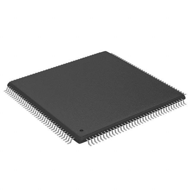
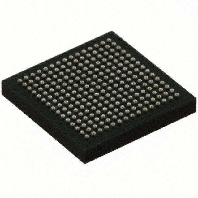
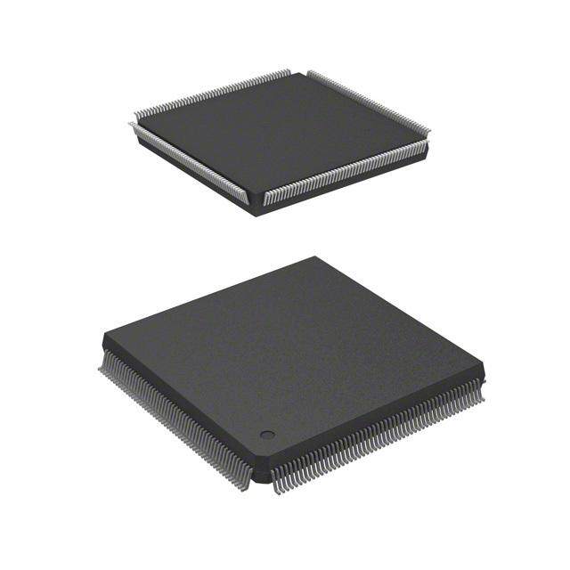
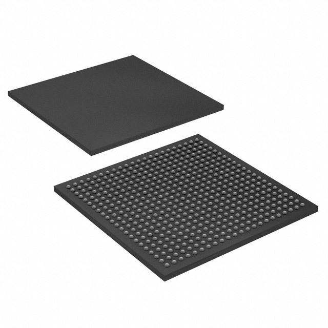
| 描述 | IC FPGA 309 I/O 484CSPBGA |
| 产品分类 | |
| I/O数 | 309 |
| LAB/CLB数 | 5968 |
| 品牌 | Xilinx Inc |
| 数据手册 | |
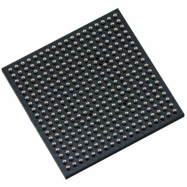
| 产品图片 |
|
| 产品型号 | XC3SD3400A-4CSG484LI |
| PCN设计/规格 | |
| rohs | 无铅 / 符合限制有害物质指令(RoHS)规范要求 |
| 产品系列 | Spartan®-3A DSP |
| 供应商器件封装 | 484-CSPBGA(19x19) |
| 其它名称 | 122-1723 |
| 安装类型 | 表面贴装 |
| 封装/外壳 | 484-FBGA,CSPBGA |
| 工作温度 | -40°C ~ 100°C |
| 总RAM位数 | 2322432 |
| 栅极数 | 3400000 |
| 标准包装 | 84 |
| 电压-电源 | 1.14 V ~ 1.26 V |
| 逻辑元件/单元数 | 53712 |


- 商务部:美国ITC正式对集成电路等产品启动337调查
- 曝三星4nm工艺存在良率问题 高通将骁龙8 Gen1或转产台积电
- 太阳诱电将投资9.5亿元在常州建新厂生产MLCC 预计2023年完工
- 英特尔发布欧洲新工厂建设计划 深化IDM 2.0 战略
- 台积电先进制程称霸业界 有大客户加持明年业绩稳了
- 达到5530亿美元!SIA预计今年全球半导体销售额将创下新高
- 英特尔拟将自动驾驶子公司Mobileye上市 估值或超500亿美元
- 三星加码芯片和SET,合并消费电子和移动部门,撤换高东真等 CEO
- 三星电子宣布重大人事变动 还合并消费电子和移动部门
- 海关总署:前11个月进口集成电路产品价值2.52万亿元 增长14.8%
PDF Datasheet 数据手册内容提取
1 Spartan-3A DSP FPGA Family Data Sheet DS610 October 4, 2010 Product Specification Module 1: Introduction and Ordering Information DS610 (v3.0) October 4, 2010 (cid:129) Introduction (cid:129) UG431: XtremeDSP™ DSP48A for Spartan-3A DSP (cid:129) Features FPGAs User Guide (cid:129) Architectural Overview (cid:129) DSP48A Slice Design Considerations (cid:129) Configuration Overview (cid:129) DSP48A Architecture Highlights (cid:129) General I/O Capabilities - 18 x 18-Bit Multipliers (cid:129) Supported Packages and Package Marking - 48-Bit Accumulator (cid:129) Ordering Information - 18-bit Pre-Adder Module 2: (cid:129) DSP48A Application Examples Functional Description Module 3: DS610 (v3.0) October 4, 2010 DC and Switching Characteristics The functionality of the Spartan®-3A DSP FPGA family is DS610 (v3.0) October 4, 2010 described in the following documents. (cid:129) DC Electrical Characteristics (cid:129) UG331: Spartan-3 Generation FPGA User Guide (cid:129) Absolute Maximum Ratings (cid:129) Clocking Resources (cid:129) Supply Voltage Specifications (cid:129) Digital Clock Managers (DCMs) (cid:129) Recommended Operating Conditions (cid:129) Block RAM (cid:129) Switching Characteristics (cid:129) Configurable Logic Blocks (CLBs) (cid:129) I/O Timing - Distributed RAM (cid:129) Configurable Logic Block (CLB) Timing - SRL16 Shift Registers (cid:129) Digital Clock Manager (DCM) Timing - Carry and Arithmetic Logic (cid:129) I/O Resources (cid:129) Block RAM Timing (cid:129) Programmable Interconnect (cid:129) XtremeDSP Slice Timing (cid:129) ISE® Software Design Tools and IP Cores (cid:129) Configuration and JTAG Timing (cid:129) Embedded Processing and Control Solutions Module 4: (cid:129) Pin Types and Package Overview Pinout Descriptions (cid:129) Package Drawings (cid:129) Powering FPGAs DS610 (v3.0) October 4, 2010 (cid:129) Power Management (cid:129) Pin Descriptions (cid:129) UG332: Spartan-3 Generation Configuration User Guide (cid:129) Package Overview (cid:129) Configuration Overview (cid:129) Pinout Tables (cid:129) Configuration Pins and Behavior (cid:129) Footprint Diagrams (cid:129) Bitstream Sizes (cid:129) Detailed Descriptions by Mode - Master Serial Mode using Platform Flash PROM - Master SPI Mode using Commodity Serial Flash - Master BPI Mode using Commodity Parallel Flash - Slave Parallel (SelectMAP) using a Processor - Slave Serial using a Processor - JTAG Mode (cid:129) ISE iMPACT Programming Examples (cid:129) MultiBoot Reconfiguration (cid:129) Design Authentication using Device DNA © Copyright 2007–2010 Xilinx, Inc. XILINX, the Xilinx logo, Virtex, Spartan, ISE, and other designated brands included herein are trademarks of Xilinx in the United States and other countries. PCI and PCI-X are trademarks of PCI-SIG and used under license. All other trademarks are the property of their respective owners. DS610 October 4, 2010 www.xilinx.com Product Specification 1
6 Spartan-3A DSP FPGA Family: Introduction and Ordering Information DS610 (v3.0) October 4, 2010 Product Specification Introduction The Spartan®-3A DSP family of Field-Programmable Gate Arrays (cid:129) Hierarchical SelectRAM™ memory architecture (FPGAs) solves the design challenges in most high- volume, (cid:129) Up to 2268 Kbits of fast block RAM with byte write enables cost-sensitive, high-performance DSP applications. The for processor applications (cid:129) Up to 373 Kbits of efficient distributed RAM two-member family offers densities ranging from 1.8 to 3.4 million (cid:129) Registered outputs on the block RAM with operation of at system gates, as shown in Table1. least 280MHz in the standard -4 speed grade The Spartan-3A DSP family builds on the success of the (cid:129) Dual-range V supply simplifies 3.3V-only design CCAUX Spartan-3A FPGA family by increasing the amount of memory per (cid:129) Suspend, Hibernate modes reduce system power logic and adding XtremeDSP™ DSP48A slices. New features (cid:129) Low-power option reduces quiescent current improve system performance and reduce the cost of configuration. (cid:129) Multi-voltage, multi-standard SelectIO™ interface pins These Spartan-3A DSP FPGA enhancements, combined with (cid:129) Up to 519 I/O pins or 227 differential signal pairs proven 90nm process technology, deliver more functionality and (cid:129) LVCMOS, LVTTL, HSTL, and SSTL single-ended I/O (cid:129) 3.3V, 2.5V, 1.8V, 1.5V, and 1.2V signaling bandwidth per dollar than ever before, setting the new standard in (cid:129) Selectable output drive, up to 24 mA per pin the programmable logic and DSP processing industry. (cid:129) QUIETIO standard reduces I/O switching noise The Spartan-3A DSP FPGAs extend and enhance the Spartan-3A (cid:129) Full 3.3V±10% compatibility and hot swap compliance FPGA family. The XC3SD1800A and the XC3SD3400A devices (cid:129) 622+ Mb/s data transfer rate per differential I/O (cid:129) LVDS, RSDS, mini-LVDS, HSTL/SSTL differential I/O with are tailored for DSP applications and have additional block RAM integrated differential termination resistors and XtremeDSP DSP48A slices. The XtremeDSP DSP48A slices (cid:129) Enhanced Double Data Rate (DDR) support replace the 18x18 multipliers found in the Spartan-3A devices and (cid:129) DDR/DDR2 SDRAM support up to 333 Mb/s are based on the DSP48 blocks found in the Virtex®-4 devices. (cid:129) Fully compliant 32-/64-bit, 33/66MHz PCI support The block RAMs are also enhanced to run faster by adding an (cid:129) Abundant, flexible logic resources output register. Both the block RAM and DSP48A slices in the (cid:129) Densities up to 53712 logic cells, including optional shift Spartan-3A DSP devices run at 250MHz in the lowest cost, register (cid:129) Efficient wide multiplexers, wide logic, fast carry logic standard -4 speed grade. (cid:129) IEEE 1149.1/1532 JTAG programming/debug port Because of their exceptional DSP price/performance ratio, (cid:129) Eight Digital Clock Managers (DCMs) Spartan-3A DSP FPGAs are ideally suited to a wide range of (cid:129) Clock skew elimination (delay locked loop) consumer electronics applications, such as broadband access, (cid:129) Frequency synthesis, multiplication, division home networking, display/projection, and digital television. (cid:129) High-resolution phase shifting (cid:129) Wide frequency range (5MHz to over 320MHz) The Spartan-3A DSP family is a superior alternative to mask (cid:129) Eight low-skew global clock networks, eight additional clocks programmed ASICs. FPGAs avoid the high initial cost, lengthy per half device, plus abundant low-skew routing development cycles, and the inherent inflexibility of conventional (cid:129) Configuration interface to industry-standard PROMs ASICs. Also, FPGA programmability permits design upgrades in (cid:129) Low-cost, space-saving SPI serial Flash PROM the field with no hardware replacement necessary, an impossibility (cid:129) x8 or x8/x16 BPI parallel NOR Flash PROM with ASICs. (cid:129) Low-cost Xilinx® Platform Flash with JTAG (cid:129) Unique Device DNA identifier for design authentication Features (cid:129) Load multiple bitstreams under FPGA control (cid:129) Post-configuration CRC checking (cid:129) Very low cost, high-performance DSP solution for (cid:129) MicroBlaze™ and PicoBlaze™ embedded processor cores high-volume, cost-conscious applications (cid:129) BGA and CSP packaging with Pb-free options (cid:129) 250MHz XtremeDSP DSP48A Slices (cid:129) Common footprints support easy density migration (cid:129) Dedicated 18-bit by 18-bit multiplier (cid:129) XA Automotive version available (cid:129) Available pipeline stages for enhanced performance of at least 250MHz in the standard -4 speed grade (cid:129) 48-bit accumulator for multiply-accumulate (MAC) operation (cid:129) Integrated adder for complex multiply or multiply-add operation (cid:129) Integrated 18-bit pre-adder (cid:129) Optional cascaded Multiply or MAC Table 1: Summary of Spartan-3A DSP FPGA Attributes CLB Array (One CLB = Four Slices) Distributed Block Maximum System Equivalent Total Total RAM RAM Maximum Differential Device Gates Logic Cells Rows Columns CLBs Slices Bits(1) Bits(1) DSP48As DCMs User I/O I/O Pairs XC3SD1800A 1800K 37,440 88 48 4,160 16,640 260K 1512K 84 8 519 227 XC3SD3400A 3400K 53,712 104 58 5,968 23,872 373K 2268K 126 8 469 213 Notes: 1. By convention, one Kb is equivalent to 1,024 bits. © Copyright 2007–2010 Xilinx, Inc. XILINX, the Xilinx logo, Virtex, Spartan, ISE, and other designated brands included herein are trademarks of Xilinx in the United States and other countries. PCI and PCI-X are trademarks of PCI-SIG and used under license. All other trademarks are the property of their respective owners. DS610 (v3.0) October 4, 2010 www.xilinx.com Product Specification 2
Spartan-3A DSP FPGA Family: Introduction and Ordering Information Architectural Overview The Spartan-3A DSP family architecture consists of five fundamental programmable functional elements: (cid:129) XtremeDSP™ DSP48A Slice provides an 18-bit x (cid:129) Digital Clock Manager (DCM) Blocks provide 18-bit multiplier, 18-bit pre-adder, 48-bit self-calibrating, fully digital solutions for distributing, post-adder/accumulator, and cascade capabilities for delaying, multiplying, dividing, and phase-shifting clock various DSP applications. signals. (cid:129) Block RAM provides data storage in the form of These elements are organized as shown in Figure1. A dual 18-Kbit dual-port blocks. ring of staggered IOBs surrounds a regular array of CLBs. (cid:129) Configurable Logic Blocks (CLBs) contain flexible The XC3SD1800A has four columns of DSP48As, and the Look-Up Tables (LUTs) that implement logic plus XC3SD3400A has five columns of DSP48As. Each storage elements used as flip-flops or latches. CLBs DSP48A has an associated block RAM. The DCMs are perform a wide variety of logical functions as well as store data. positioned in the center with two at the top and two at the bottom of the device and in the two outer columns of the 4 or (cid:129) Input/Output Blocks (IOBs) control the flow of data between the I/O pins and the internal logic of the 5 columns of block RAM and DSP48As. device. IOBs support bidirectional data flow plus The Spartan-3A DSP family features a rich network of 3-state operation. Supports a variety of signal standards, including several high-performance routing that interconnect all five functional elements, differential standards. Double Data-Rate (DDR) transmitting signals among them. Each functional element registers are included. has an associated switch matrix that permits multiple connections to the routing. X-Ref Target - Figure 1 IOBs CLB e M c A Sli R A DCM k 8 c 4 o P Bl S D IOBs DCM ce Sli A 8 4 CLBs P S OBs DCM M / D OBs I RA I k c o Bl IOBs DS610-1_01_031207 Notes: 1. The XC3SD1800A and XC3SD3400A have two DCMs on both the left and right sides, as well as the two DCMs at the top and bottom of the devices. The two DCMs on the left and right of the chips are in the middle of the outer Block RAM/DSP48A columns of the 4 or 5 columns in the selected device, as shown in the diagram above. 2. A detailed diagram of the DSP48A can be found in UG431: XtremeDSP DSP48A for Spartan-3A DSP FPGAs User Guide. Figure 1: Spartan-3A DSP Family Architecture DS610 (v3.0) October 4, 2010 www.xilinx.com Product Specification 3
Spartan-3A DSP FPGA Family: Introduction and Ordering Information Configuration I/O Capabilities Spartan-3A DSP FPGAs are programmed by loading The Spartan-3A DSP FPGA SelectIO interface supports configuration data into robust, reprogrammable, static many popular single-ended and differential standards. CMOS configuration latches (CCLs) that collectively control Table2 shows the number of user I/Os as well as the all functional elements and routing resources. The FPGA’s number of differential I/O pairs available for each configuration data is stored externally in a PROM or some device/package combination. Some of the user I/Os are other non-volatile medium, either on or off the board. After unidirectional input-only pins as indicated in Table2. applying power, the configuration data is written to the Spartan-3A DSP FPGAs support the following single-ended FPGA using any of seven different modes: standards: (cid:129) Master Serial from a Xilinx Platform Flash PROM (cid:129) 3.3V low-voltage TTL (LVTTL) (cid:129) Serial Peripheral Interface (SPI) from an (cid:129) Low-voltage CMOS (LVCMOS) at 3.3V, 2.5V, 1.8V, industry-standard SPI serial Flash 1.5V, or 1.2V (cid:129) Byte Peripheral Interface (BPI) Up from an (cid:129) 3.3V PCI at 33MHz or 66MHz industry-standard x8 or x8/x16 parallel NOR Flash (cid:129) HSTL I, II, and III at 1.5V and 1.8V, commonly used in (cid:129) Slave Serial, typically downloaded from a processor memory applications (cid:129) Slave Parallel, typically downloaded from a processor (cid:129) SSTL I and II at 1.8V, 2.5V, and 3.3V, commonly used (cid:129) Boundary Scan (JTAG), typically downloaded from a for memory applications processor or system tester (cid:129) Spartan-3A DSP FPGAs support the following Furthermore, Spartan-3A DSP FPGAs support MultiBoot differential standards: configuration, allowing two or more FPGA configuration (cid:129) LVDS, mini-LVDS, RSDS, and PPDS I/O at 2.5V or bitstreams to be stored in a single SPI serial Flash or a BPI 3.3V parallel NOR Flash. The FPGA application controls which (cid:129) Bus LVDS I/O at 2.5V configuration to load next and when to load it. (cid:129) TMDS I/O at 3.3V Additionally, each Spartan-3A DSP FPGA contains a unique, factory-programmed Device DNA identifier useful (cid:129) Differential HSTL and SSTL I/O for tracking purposes, anti-cloning designs, or IP protection. (cid:129) LVPECL inputs at 2.5V or 3.3V Table 2: Available User I/Os and Differential (Diff) I/O Pairs CS484 FG676 CSG484 FGG676 Device User Diff User Diff 309(1) 140 519 227 XC3SD1800A (60) (78) (110) (131) 309 140 469 213 XC3SD3400A (60) (78) (60) (117) Notes: 1. The number shown in bold indicates the maximum number of I/O and input-only pins. The number shown in (italics) indicates the number of input-only pins. The differential (Diff) input-only pin count includes both differential pairs on input-only pins and differential pairs on I/O pins within I/O banks that are restricted to differential inputs. DS610 (v3.0) October 4, 2010 www.xilinx.com Product Specification 4
Spartan-3A DSP FPGA Family: Introduction and Ordering Information Package Marking Figure2 shows the top marking for Spartan-3A DSP FPGAs. The “5C” and “4I” Speed Grade/Temperature Range part combinations may be dual marked as “5C/4I”. Devices with the dual mark can be used as either -5C or -4I devices. Devices with a single mark are only guaranteed for the marked speed grade and temperature range. X-Ref Target - Figure 2 Mask Revision BGA Ball A1 R SPARTANR Fabrication/ Process Code Device Type XC3SD1800A Package CSG484XGQ#### Date Code X#######X Lot Code Low-Power (optional) L4I Speed Grade Operating Range DS610-1_02_070607 Figure 2: Spartan-3A DSP FPGA Package Marking Example Ordering Information Spartan-3A DSP FPGAs are available in both standard and Pb-free packaging options for all device/package combinations. The Pb-free packages include a ‘G’ character in the ordering code. Example: XC3SD1800A -4 CS 484 LI Device Type Power/Temperature Range Speed Grade Number of Pins Package Type DS610-1_05_021009 Power/Temperature Range Device Speed Grade Package Type / Number of Pins (T ) J XC3SD1800A -4 Standard Performance CS484/ 484-ball Chip-Scale Ball Grid Array (CSBGA) C Commercial (0°C to 85°C) CSG484 XC3SD3400A -5 High Performance(1) FG676/ 676-ball Fine-Pitch Ball Grid Array (FBGA) I Industrial (–40°C to 100°C) FGG676 LI Low-power Industrial (–40°C to 100°C)(2) Notes: 1. The -5 speed grade is exclusively available in the Commercial temperature range. 2. The low-power option (LI) is exclusively available in the CS(G)484 package and industrial temperature range. 3. See DS705, XA Spartan-3A DSP Automotive FPGA Family Data Sheet for the XA Automotive Spartan-3A DSP FPGAs. DS610 (v3.0) October 4, 2010 www.xilinx.com Product Specification 5
Spartan-3A DSP FPGA Family: Introduction and Ordering Information Revision History The following table shows the revision history for this document. Date Version Revision 04/02/07 1.0 Initial Xilinx release. 05/25/07 1.0.1 Minor edits. 06/18/07 1.2 Updated for Production release. 07/16/07 2.0 Added Low-power options. 06/02/08 2.1 Added reference to SCD 4103 for 750 Mbps performance. Add dual mark clarification to Package Marking. Updated links. 03/11/09 2.2 Simplified ordering information. Removed reference to SCD 4103. 10/04/10 3.0 Updated the Notice of Disclaimer section. Notice of Disclaimer THE XILINX HARDWARE FPGA AND CPLD DEVICES REFERRED TO HEREIN (“PRODUCTS”) ARE SUBJECT TO THE TERMS AND CONDITIONS OF THE XILINX LIMITED WARRANTY WHICH CAN BE VIEWED AT http://www.xilinx.com/warranty.htm. THIS LIMITED WARRANTY DOES NOT EXTEND TO ANY USE OF PRODUCTS IN AN APPLICATION OR ENVIRONMENT THAT IS NOT WITHIN THE SPECIFICATIONS STATED IN THE XILINX DATA SHEET. ALL SPECIFICATIONS ARE SUBJECT TO CHANGE WITHOUT NOTICE. PRODUCTS ARE NOT DESIGNED OR INTENDED TO BE FAIL-SAFE OR FOR USE IN ANY APPLICATION REQUIRING FAIL-SAFE PERFORMANCE, SUCH AS LIFE-SUPPORT OR SAFETY DEVICES OR SYSTEMS, OR ANY OTHER APPLICATION THAT INVOKES THE POTENTIAL RISKS OF DEATH, PERSONAL INJURY, OR PROPERTY OR ENVIRONMENTAL DAMAGE (“CRITICAL APPLICATIONS”). USE OF PRODUCTS IN CRITICAL APPLICATIONS IS AT THE SOLE RISK OF CUSTOMER, SUBJECT TO APPLICABLE LAWS AND REGULATIONS. CRITICAL APPLICATIONS DISCLAIMER XILINX PRODUCTS (INCLUDING HARDWARE, SOFTWARE AND/OR IP CORES) ARE NOT DESIGNED OR INTENDED TO BE FAIL-SAFE, OR FOR USE IN ANY APPLICATION REQUIRING FAIL-SAFE PERFORMANCE, SUCH AS IN LIFE-SUPPORT OR SAFETY DEVICES OR SYSTEMS, CLASS III MEDICAL DEVICES, NUCLEAR FACILITIES, APPLICATIONS RELATED TO THE DEPLOYMENT OF AIRBAGS, OR ANY OTHER APPLICATIONS THAT COULD LEAD TO DEATH, PERSONAL INJURY OR SEVERE PROPERTY OR ENVIRONMENTAL DAMAGE (INDIVIDUALLY AND COLLECTIVELY, “CRITICAL APPLICATIONS”). FURTHERMORE, XILINX PRODUCTS ARE NOT DESIGNED OR INTENDED FOR USE IN ANY APPLICATIONS THAT AFFECT CONTROL OF A VEHICLE OR AIRCRAFT, UNLESS THERE IS A FAIL-SAFE OR REDUNDANCY FEATURE (WHICH DOES NOT INCLUDE USE OF SOFTWARE IN THE XILINX DEVICE TO IMPLEMENT THE REDUNDANCY) AND A WARNING SIGNAL UPON FAILURE TO THE OPERATOR. CUSTOMER AGREES, PRIOR TO USING OR DISTRIBUTING ANY SYSTEMS THAT INCORPORATE XILINX PRODUCTS, TO THOROUGHLY TEST THE SAME FOR SAFETY PURPOSES. TO THE MAXIMUM EXTENT PERMITTED BY APPLICABLE LAW, CUSTOMER ASSUMES THE SOLE RISK AND LIABILITY OF ANY USE OF XILINX PRODUCTS IN CRITICAL APPLICATIONS. AUTOMOTIVE APPLICATIONS DISCLAIMER XILINX PRODUCTS ARE NOT DESIGNED OR INTENDED TO BE FAIL-SAFE, OR FOR USE IN ANY APPLICATION REQUIRING FAIL-SAFE PERFORMANCE, SUCH AS APPLICATIONS RELATED TO: (I) THE DEPLOYMENT OF AIRBAGS, (II) CONTROL OF A VEHICLE, UNLESS THERE IS A FAIL-SAFE OR REDUNDANCY FEATURE (WHICH DOES NOT INCLUDE USE OF SOFTWARE IN THE XILINX DEVICE TO IMPLEMENT THE REDUNDANCY) AND A WARNING SIGNAL UPON FAILURE TO THE OPERATOR, OR (III) USES THAT COULD LEAD TO DEATH OR PERSONAL INJURY. CUSTOMER ASSUMES THE SOLE RISK AND LIABILITY OF ANY USE OF XILINX PRODUCTS IN SUCH APPLICATIONS. DS610 (v3.0) October 4, 2010 www.xilinx.com Product Specification 6
8 Spartan-3A DSP FPGA Family: Functional Description DS610 (v3.0) October 4, 2010 Product Specification Spartan-3A DSP FPGA Design Documentation The functionality of the Spartan®-3A DSP FPGA family is described in the following documents. The topics covered in each guide are listed. (cid:129) DS706: Extended Spartan-3A Family Overview (cid:129) UG431: XtremeDSP DSP48A for Spartan-3A DSP FPGAs User Guide (cid:129) UG331: Spartan-3 Generation FPGA User Guide (cid:129) XtremeDSP DSP48A Slices (cid:129) Clocking Resources (cid:129) Digital Clock Managers (DCMs) (cid:129) XtremeDSP DSP48A Pre-Adder (cid:129) Block RAM For specific hardware examples, please see the Spartan-3A (cid:129) Configurable Logic Blocks (CLBs) DSP FPGA Starter Kit board web pages. - Distributed RAM (cid:129) XtremeDSP Starter Platform—Spartan-3A DSP - SRL16 Shift Registers 1800A Edition - Carry and Arithmetic Logic http://www.xilinx.com/products/devkits (cid:129) I/O Resources /HW-SD1800A-DSP-SB-UNI-G.htm (cid:129) Programmable Interconnect (cid:129) XtremeDSP Starter Kit—Spartan-3A DSP 1800A (cid:129) ISE® Software Design Tools Edition http://www.xilinx.com/products/devkits (cid:129) IP Cores /DO-SD1800A-DSP-SK-UNI-G.htm (cid:129) Embedded Processing and Control Solutions (cid:129) XtremeDSP Video Starter Kit—Spartan-3A DSP (cid:129) Pin Types and Package Overview Edition (cid:129) Package Drawings http://www.xilinx.com/products/devkits (cid:129) Powering FPGAs /DO-S3ADSP-VIDEO-SK-UNI-G.htm (cid:129) Power Management (cid:129) Embedded Development HW/SW Kit—Spartan-3A (cid:129) UG332: Spartan-3 Generation Configuration User DSP S3D1800A MicroBlaze Processor Edition Guide http://www.xilinx.com/products/devkits (cid:129) Configuration Overview /DO-SD1800A-EDK-DK-UNI-G.htm - Configuration Pins and Behavior Create a Xilinx user account and sign up to receive - Bitstream Sizes automatic e-mail notification whenever this data sheet or (cid:129) Detailed Descriptions by Mode the associated user guides are updated. - Master Serial Mode using Xilinx Platform Flash (cid:129) Sign Up for Alerts on Xilinx.com PROM https://secure.xilinx.com/webreg/register.do?group=my - Master SPI Mode using Commodity SPI Serial profile&languageID=1 Flash PROM - Master BPI Mode using Commodity Parallel NOR Flash PROM - Slave Parallel (SelectMAP) using a Processor - Slave Serial using a Processor - JTAG Mode (cid:129) ISE iMPACT Programming Examples (cid:129) MultiBoot Reconfiguration (cid:129) Design Authentication using Device DNA © Copyright 2007–2010 Xilinx, Inc. XILINX, the Xilinx logo, Virtex, Spartan, ISE, and other designated brands included herein are trademarks of Xilinx in the United States and other countries. PCI and PCI-X are trademarks of PCI-SIG and used under license. All other trademarks are the property of their respective owners. DS610 (v3.0) October 4, 2010 www.xilinx.com Product Specification 7
Spartan-3A DSP FPGA Family: Functional Description Revision History The following table shows the revision history for this document. Date Version Revision 04/02/07 1.0 Initial Xilinx release. 05/25/07 1.0.1 Minor edits. 06/18/07 1.2 Updated for Production release. 07/16/07 2.0 Added Low-power options; no changes to this module. 06/02/08 2.1 Updated links. 03/11/09 2.2 Added link to DS706 on Extended Spartan-3A family. 10/04/10 3.0 Updated link to sign up for Alerts and updated Notice of Disclaimer. Notice of Disclaimer THE XILINX HARDWARE FPGA AND CPLD DEVICES REFERRED TO HEREIN (“PRODUCTS”) ARE SUBJECT TO THE TERMS AND CONDITIONS OF THE XILINX LIMITED WARRANTY WHICH CAN BE VIEWED AT http://www.xilinx.com/warranty.htm. THIS LIMITED WARRANTY DOES NOT EXTEND TO ANY USE OF PRODUCTS IN AN APPLICATION OR ENVIRONMENT THAT IS NOT WITHIN THE SPECIFICATIONS STATED IN THE XILINX DATA SHEET. ALL SPECIFICATIONS ARE SUBJECT TO CHANGE WITHOUT NOTICE. PRODUCTS ARE NOT DESIGNED OR INTENDED TO BE FAIL-SAFE OR FOR USE IN ANY APPLICATION REQUIRING FAIL-SAFE PERFORMANCE, SUCH AS LIFE-SUPPORT OR SAFETY DEVICES OR SYSTEMS, OR ANY OTHER APPLICATION THAT INVOKES THE POTENTIAL RISKS OF DEATH, PERSONAL INJURY, OR PROPERTY OR ENVIRONMENTAL DAMAGE (“CRITICAL APPLICATIONS”). USE OF PRODUCTS IN CRITICAL APPLICATIONS IS AT THE SOLE RISK OF CUSTOMER, SUBJECT TO APPLICABLE LAWS AND REGULATIONS. CRITICAL APPLICATIONS DISCLAIMER XILINX PRODUCTS (INCLUDING HARDWARE, SOFTWARE AND/OR IP CORES) ARE NOT DESIGNED OR INTENDED TO BE FAIL-SAFE, OR FOR USE IN ANY APPLICATION REQUIRING FAIL-SAFE PERFORMANCE, SUCH AS IN LIFE-SUPPORT OR SAFETY DEVICES OR SYSTEMS, CLASS III MEDICAL DEVICES, NUCLEAR FACILITIES, APPLICATIONS RELATED TO THE DEPLOYMENT OF AIRBAGS, OR ANY OTHER APPLICATIONS THAT COULD LEAD TO DEATH, PERSONAL INJURY OR SEVERE PROPERTY OR ENVIRONMENTAL DAMAGE (INDIVIDUALLY AND COLLECTIVELY, “CRITICAL APPLICATIONS”). FURTHERMORE, XILINX PRODUCTS ARE NOT DESIGNED OR INTENDED FOR USE IN ANY APPLICATIONS THAT AFFECT CONTROL OF A VEHICLE OR AIRCRAFT, UNLESS THERE IS A FAIL-SAFE OR REDUNDANCY FEATURE (WHICH DOES NOT INCLUDE USE OF SOFTWARE IN THE XILINX DEVICE TO IMPLEMENT THE REDUNDANCY) AND A WARNING SIGNAL UPON FAILURE TO THE OPERATOR. CUSTOMER AGREES, PRIOR TO USING OR DISTRIBUTING ANY SYSTEMS THAT INCORPORATE XILINX PRODUCTS, TO THOROUGHLY TEST THE SAME FOR SAFETY PURPOSES. TO THE MAXIMUM EXTENT PERMITTED BY APPLICABLE LAW, CUSTOMER ASSUMES THE SOLE RISK AND LIABILITY OF ANY USE OF XILINX PRODUCTS IN CRITICAL APPLICATIONS. AUTOMOTIVE APPLICATIONS DISCLAIMER XILINX PRODUCTS ARE NOT DESIGNED OR INTENDED TO BE FAIL-SAFE, OR FOR USE IN ANY APPLICATION REQUIRING FAIL-SAFE PERFORMANCE, SUCH AS APPLICATIONS RELATED TO: (I) THE DEPLOYMENT OF AIRBAGS, (II) CONTROL OF A VEHICLE, UNLESS THERE IS A FAIL-SAFE OR REDUNDANCY FEATURE (WHICH DOES NOT INCLUDE USE OF SOFTWARE IN THE XILINX DEVICE TO IMPLEMENT THE REDUNDANCY) AND A WARNING SIGNAL UPON FAILURE TO THE OPERATOR, OR (III) USES THAT COULD LEAD TO DEATH OR PERSONAL INJURY. CUSTOMER ASSUMES THE SOLE RISK AND LIABILITY OF ANY USE OF XILINX PRODUCTS IN SUCH APPLICATIONS. DS610 (v3.0) October 4, 2010 www.xilinx.com Product Specification 8
61 Spartan-3A DSP FPGA Family: DC and Switching Characteristics DS610 (v3.0) October 4, 2010 Product Specification DC Electrical Characteristics In this section, specifications may be designated as All parameter limits are representative of worst-case supply Advance, Preliminary, or Production. These terms are voltage and junction temperature conditions. Unless defined as follows: otherwise noted, the published parameter values apply to all Spartan®-3A DSP devices. AC and DC Advance: Initial estimates are based on simulation, early characteristics are specified using the same numbers characterization, and/or extrapolation from the for both commercial and industrial grades. characteristics of other families. Values are subject to change. Use as estimates, not for production. Absolute Maximum Ratings Preliminary: Based on characterization. Further changes are not expected. Stresses beyond those listed under Table3: Absolute Maximum Ratings may cause permanent damage to the Production: These specifications are approved once the device. These are stress ratings only; functional operation silicon has been characterized over numerous production of the device at these or any other conditions beyond those lots. Parameter values are considered stable with no future listed under the Recommended Operating Conditions is not changes expected. implied. Exposure to absolute maximum conditions for extended periods of time adversely affects device reliability. Table 3: Absolute Maximum Ratings Symbol Description Conditions Min Max Units V Internal supply voltage –0.5 1.32 V CCINT V Auxiliary supply voltage –0.5 3.75 V CCAUX V Output driver supply voltage –0.5 3.75 V CCO V Input reference voltage –0.5 V +0.5 V REF CCO V Voltage applied to all User I/O pins and –0.95 4.6 V IN Dual-Purpose pins Driver in a high-impedance state Voltage applied to all Dedicated pins –0.5 4.6 V I Input clamp current per I/O pin –0.5V<V <(V +0.5V)(1) – ±100 mA IK IN CCO V Electrostatic Discharge Voltage Human body model – ±2000 V ESD Charged device model – ±500 V Machine model – ±200 V T Junction temperature – 125 °C J T Storage temperature –65 150 °C STG Notes: 1. Upper clamp applies only when using PCI IOSTANDARDs. 2. For soldering guidelines, see UG112: Device Packaging and Thermal Characteristics and XAPP427: Implementation and Solder Reflow Guidelines for Pb-Free Packages. © Copyright 2007–2010 Xilinx, Inc. XILINX, the Xilinx logo, Virtex, Spartan, ISE, and other designated brands included herein are trademarks of Xilinx in the United States and other countries. PCI and PCI-X are trademarks of PCI-SIG and used under license. All other trademarks are the property of their respective owners. DS610 (v3.0) October 4, 2010 www.xilinx.com Product Specification 9
Spartan-3A DSP FPGA Family: DC and Switching Characteristics Power Supply Specifications Table 4: Supply Voltage Thresholds for Power-On Reset Symbol Description Min Max Units V Threshold for the V supply 0.4 1.0 V CCINTT CCINT V Threshold for the V supply 1.0 2.0 V CCAUXT CCAUX V Threshold for the V Bank 2 supply 1.0 2.0 V CCO2T CCO Notes: 1. V , V , and V supplies to the FPGA can be applied in any order. However, the FPGA configuration source (Platform Flash, SPI CCINT CCAUX CCO Flash, parallel NOR Flash, microcontroller) might have specific requirements. Check the data sheet for the attached configuration source. Apply V last for lowest overall power consumption (see the UG331 chapter titled "Powering Spartan-3 Generation FPGAs" for more CCINT information). 2. To ensure successful power-on, V , V Bank 2, and V supplies must rise through their respective threshold-voltage ranges with CCINT CCO CCAUX no dips at any point. Table 5: Supply Voltage Ramp Rate Symbol Description Min Max Units V Ramp rate from GND to valid V supply level 0.2 100 ms CCINTR CCINT V Ramp rate from GND to valid V supply level 0.2 100 ms CCAUXR CCAUX V Ramp rate from GND to valid V Bank 2 supply level 0.2 100 ms CCO2R CCO Notes: 1. V , V , and V supplies to the FPGA can be applied in any order. However, the FPGA configuration source (Platform Flash, SPI CCINT CCAUX CCO Flash, parallel NOR Flash, microcontroller) might have specific requirements. Check the data sheet for the attached configuration source. Apply V last for lowest overall power consumption (see the UG331 chapter titled "Powering Spartan-3 Generation FPGAs" for more CCINT information). 2. To ensure successful power-on, V , V Bank 2, and V supplies must rise through their respective threshold-voltage ranges with CCINT CCO CCAUX no dips at any point. Table 6: Supply Voltage Levels Necessary for Preserving CMOS Configuration Latch (CCL) Contents and RAM Data Symbol Description Min Units V V level required to retain CMOS Configuration Latch (CCL) and RAM data 1.0 V DRINT CCINT V V level required to retain CMOS Configuration Latch (CCL) and RAM data 2.0 V DRAUX CCAUX DS610 (v3.0) October 4, 2010 www.xilinx.com Product Specification 10
Spartan-3A DSP FPGA Family: DC and Switching Characteristics General Recommended Operating Conditions Table 7: General Recommended Operating Conditions Symbol Description Min Nominal Max Units T Junction temperature Commercial 0 – 85 °C J Industrial –40 – 100 °C V Internal supply voltage 1.14 1.20 1.26 V CCINT V (1) Output driver supply voltage 1.10 – 3.60 V CCO V Auxiliary supply voltage(2) V =2.5 2.25 2.50 2.75 V CCAUX CCAUX V =3.3 3.00 3.30 3.60 V CCAUX V (3) Input voltage PCI™ IOSTANDARD –0.5 – V +0.5 V IN CCO All other IP or IO_# –0.5 – 4.10 V IOSTANDARDs IO_Lxxy_#(4) –0.5 – 4.10 V T Input signal transition time(5) – – 500 ns IN Notes: 1. This V range spans the lowest and highest operating voltages for all supported I/O standards. Table10 lists the recommended V CCO CCO range specific to each of the single-ended I/O standards, and Table12 lists that specific to the differential standards. 2. Define V selection using CONFIG VCCAUX constraint. CCAUX 3. See XAPP459, Eliminating I/O Coupling Effects when Interfacing Large-Swing Single-Ended Signals to User I/O Pins on Spartan-3 Families. 4. For single-ended signals that are placed on a differential-capable I/O, V of –0.2V to –0.5V is supported but can cause increased leakage IN between the two pins. See Parasitic Leakage in UG331, Spartan-3 Generation FPGA User Guide. 5. Measured between 10% and 90% V . Follow Signal Integrity recommendations. CCO DS610 (v3.0) October 4, 2010 www.xilinx.com Product Specification 11
Spartan-3A DSP FPGA Family: DC and Switching Characteristics General DC Characteristics for I/O Pins Table 8: General DC Characteristics of User I/O, Dual-Purpose, and Dedicated Pins(1) Symbol Description Test Conditions Min Typ Max Units I (2) Leakage current at User I/O, Driver is in a high-impedance state, –10 – +10 µA L Input-only, Dual-Purpose, and V =0V or V max, sample-tested IN CCO Dedicated pins, FPGA powered I Leakage current on pins during All pins except INIT_B, PROG_B, DONE, and JTAG pins –10 – +10 µA HS hot socketing, FPGA unpowered when PUDC_B=1. INIT_B, PROG_B, DONE, and JTAG pins or other pins Add I + I µA HS RPU when PUDC_B=0. I (3) Current through pull-up resistor V = GND V or V = 3.0V to 3.6V –151 –315 –710 µA RPU IN CCO CCAUX at User I/O, Dual-Purpose, V or V = 2.3V to 2.7V –82 –182 –437 µA Input-only, and Dedicated pins. CCO CCAUX Dedicated pins are powered by V = 1.7V to 1.9V –36 –88 –226 µA CCO V . CCAUX V = 1.4V to 1.6V –22 –56 –148 µA CCO V = 1.14V to 1.26V –11 –31 –83 µA CCO R (3) Equivalent pull-up resistor value V = GND V = 3.0V to 3.6V 5.1 11.4 23.9 kΩ PU IN CCO at User I/O, Dual-Purpose, V = 2.3V to 2.7V 6.2 14.8 33.1 kΩ Input-only, and Dedicated pins CCO (based on IRPU per Note 2) VCCO = 1.7V to 1.9V 8.4 21.6 52.6 kΩ V = 1.4V to 1.6V 10.8 28.4 74.0 kΩ CCO V = 1.14V to 1.26V 15.3 41.1 119.4 kΩ CCO I (3) Current through pull-down V = V V = 3.0V to 3.6V 167 346 659 µA RPD IN CCO CCAUX resistor at User I/O, V = 2.25V to 2.75V Dual-Purpose, Input-only, and CCAUX 100 225 457 µA Dedicated pins R (3) Equivalent pull-down resistor V = 3.0V to 3.6V V = 3.0V to 3.6V 5.5 10.4 20.8 kΩ PD CCAUX IN value at User I/O, Dual-Purpose, V = 2.3V to 2.7V 4.1 7.8 15.7 kΩ Input-only, and Dedicated pins IN (based on IRPD per Note 2) VIN = 1.7V to 1.9V 3.0 5.7 11.1 kΩ V = 1.4V to 1.6V 2.7 5.1 9.6 kΩ IN V = 1.14V to 1.26V 2.4 4.5 8.1 kΩ IN V = 2.25V to 2.75V V = 3.0V to 3.6V 7.9 16.0 35.0 kΩ CCAUX IN V = 2.3V to 2.7V 5.9 12.0 26.3 kΩ IN V = 1.7V to 1.9V 4.2 8.5 18.6 kΩ IN V = 1.4V to 1.6V 3.6 7.2 15.7 kΩ IN V = 1.14V to 1.26V 3.0 6.0 12.5 kΩ IN I V current per pin All V levels –10 – +10 µA REF REF CCO C Input capacitance – – – 10 pF IN R Resistance of optional V = 3.3V±10% LVDS_33, MINI_LVDS_33, 90 100 115 Ω DT CCO differential termination circuit RSDS_33 within a differential I/O pair. Not V = 2.5V±10% LVDS_25, MINI_LVDS_25, 90 110 – Ω available on Input-only pairs. CCO RSDS_25 Notes: 1. The numbers in this table are based on the conditions set forth in Table7. 2. For single-ended signals that are placed on a differential-capable I/O, V of –0.2V to –0.5V is supported but can cause increased leakage IN between the two pins. See Parasitic Leakage in UG331, Spartan-3 Generation FPGA User Guide. 3. This parameter is based on characterization. The pull-up resistance R = V /I . The pull-down resistance R =V /I . PU CCO RPU PD IN RPD DS610 (v3.0) October 4, 2010 www.xilinx.com Product Specification 12
Spartan-3A DSP FPGA Family: DC and Switching Characteristics Quiescent Current Requirements Table 9: Quiescent Supply Current Characteristics(1) Commercial Industrial Symbol Description Device Power Typical(2) Units Maximum(2) Maximum(2) I Quiescent V supply current XC3SD1800A C,I 41 390 500 mA CCINTQ CCINT LI 36 – 175 mA XC3SD3400A C,I 64 550 725 mA LI 55 – 300 mA I Quiescent V supply current XC3SD1800A C,I 0.4 4 5 mA CCOQ CCO LI 0.2 – 5 mA XC3SD3400A C,I 0.4 4 5 mA LI 0.2 – 5 mA I Quiescent V supply current XC3SD1800A C,I 25 90 110 mA CCAUXQ CCAUX LI 24 – 72 mA XC3SD3400A C,I 39 130 160 mA LI 38 – 105 mA Notes: 1. The numbers in this table are based on the conditions set forth in Table7. 2. Quiescent supply current is measured with all I/O drivers in a high-impedance state and with all pull-up/pull-down resistors at the I/O pads disabled. Typical values are characterized using typical devices at room temperature (T of 25°C at V = 1.2V, V = 3.3V, and V J CCINT CCO CCAUX = 2.5V). The maximum limits are tested for each device at the respective maximum specified junction temperature and at maximum voltage limits with V = 1.26V, V = 3.6V, and V = 3.6V. The FPGA is programmed with a “blank” configuration data file (that is, a design CCINT CCO CCAUX with no functional elements instantiated). For conditions other than those described above (for example, a design including functional elements), measured quiescent current levels will be different than the values in the table. 3. For more accurate estimates for a specific design, use the Xilinx XPower tools. There are two recommended ways to estimate the total power consumption (quiescent plus dynamic) for a specific design: a) The Spartan-3A DSP FPGA XPower Estimator provides quick, approximate, typical estimates, and does not require a netlist of the design. b) XPower Analyzer uses a netlist as input to provide maximum estimates as well as more accurate typical estimates. 4. The maximum numbers in this table indicate the minimum current each power rail requires in order for the FPGA to power-on successfully. 5. For information on the power-saving Suspend mode, see XAPP480: Using Suspend Mode in Spartan-3 Generation FPGAs. Suspend mode typically saves 40% total power consumption compared to quiescent current. DS610 (v3.0) October 4, 2010 www.xilinx.com Product Specification 13
Spartan-3A DSP FPGA Family: DC and Switching Characteristics Single-Ended I/O Standards Table 10: Recommended Operating Conditions for User I/Os Using Single-Ended Standards IOSTANDARD VCCO for Drivers(2) VREF VIL VIH(3) Attribute Min (V) Nom (V) Max (V) Min (V) Nom (V) Max (V) Max (V) Min (V) LVTTL 3.0 3.3 3.6 0.8 2.0 LVCMOS33(4) 3.0 3.3 3.6 0.8 2.0 LVCMOS25(4,5) 2.3 2.5 2.7 0.7 1.7 LVCMOS18 1.65 1.8 1.95 V is not used for 0.4 0.8 REF LVCMOS15 1.4 1.5 1.6 these I/O standards 0.4 0.8 LVCMOS12 1.1 1.2 1.3 0.4 0.7 PCI33_3(6) 3.0 3.3 3.6 0.3• V 0.5• V CCO CCO PCI66_3(6) 3.0 3.3 3.6 0.3• V 0.5• V CCO CCO HSTL_I 1.4 1.5 1.6 0.68 0.75 0.9 V –0.1 V +0.1 REF REF HSTL_III 1.4 1.5 1.6 – 0.9 – V –0.1 V +0.1 REF REF HSTL_I_18 1.7 1.8 1.9 0.8 0.9 1.1 V –0.1 V +0.1 REF REF HSTL_II_18 1.7 1.8 1.9 – 0.9 – V –0.1 V +0.1 REF REF HSTL_III_18 1.7 1.8 1.9 – 1.1 – V –0.1 V +0.1 REF REF SSTL18_I 1.7 1.8 1.9 0.833 0.900 0.969 V –0.125 V +0.125 REF REF SSTL18_II 1.7 1.8 1.9 0.833 0.900 0.969 V –0.125 V +0.125 REF REF SSTL2_I 2.3 2.5 2.7 1.13 1.25 1.38 V –0.150 V +0.150 REF REF SSTL2_II 2.3 2.5 2.7 1.13 1.25 1.38 V –0.150 V +0.150 REF REF SSTL3_I 3.0 3.3 3.6 1.3 1.5 1.7 V –0.2 V +0.2 REF REF SSTL3_II 3.0 3.3 3.6 1.3 1.5 1.7 V –0.2 V +0.2 REF REF Notes: 1. Descriptions of the symbols used in this table are as follows: V —the supply voltage for output drivers CCO V —the reference voltage for setting the input switching threshold REF V —the input voltage that indicates a Low logic level IL V —the input voltage that indicates a High logic level IH 2. In general, the V rails supply only output drivers, not input circuits. The exceptions are for LVCMOS25 inputs when V =3.3V range CCO CCAUX and for PCI I/O standards. 3. For device operation, the maximum signal voltage (V max) can be as high as V max. See Table7. IH IN 4. There is approximately 100 mV of hysteresis on inputs using LVCMOS33 and LVCMOS25 I/O standards. 5. All Dedicated pins (PROG_B, DONE, SUSPEND, TCK, TDI, TDO, and TMS) draw power from the V rail and use the LVCMOS25 or CCAUX LVCMOS33 standard depending on V . The Dual-Purpose configuration pins use the LVCMOS standard before the User mode. When CCAUX using these pins as part of a standard 2.5V configuration interface, apply 2.5V to the V lines of Banks 0, 1, and 2 at power-on as well as CCO throughout configuration. 6. For information on PCI IP solutions, see www.xilinx.com/pci. The PCI IOSTANDARD is not supported on input-only pins. The PCIX IOSTANDARD is available and has equivalent characteristics but no PCI-X IP is supported. DS610 (v3.0) October 4, 2010 www.xilinx.com Product Specification 14
Spartan-3A DSP FPGA Family: DC and Switching Characteristics Table 11: DC Characteristics of User I/Os Using Table 11: DC Characteristics of User I/Os Using Single-Ended Standards Single-Ended Standards (Cont’d) Test Logic Level Test Logic Level IOSTANDARD Conditions Characteristics IOSTANDARD Conditions Characteristics Attribute IOL IOH VOL VOH Attribute IOL IOH VOL VOH (mA) (mA) Max (V) Min (V) (mA) (mA) Max (V) Min (V) LVTTL(3) 2 2 –2 0.4 2.4 PCI33_3(4) 1.5 –0.5 10% VCCO 90% VCCO 4 4 –4 PCI66_3(4) 1.5 –0.5 10% VCCO 90% VCCO 6 6 –6 HSTL_I(5) 8 –8 0.4 VCCO–0.4 8 8 –8 HSTL_III(5) 24 –8 0.4 VCCO–0.4 12 12 –12 HSTL_I_18 8 –8 0.4 VCCO–0.4 16 16 –16 HSTL_II_18(5) 16 –16 0.4 VCCO–0.4 24 24 –24 HSTL_III_18 24 –8 0.4 VCCO–0.4 LVCMOS33(3) 2 2 –2 0.4 VCCO–0.4 SSTL18_I 6.7 –6.7 VTT–0.475 VTT+0.475 4 4 –4 SSTL18_II(5) 13.4 –13.4 VTT–0.603 VTT+0.603 6 6 –6 SSTL2_I 8.1 –8.1 VTT–0.61 VTT+0.61 8 8 –8 SSTL2_II(5) 16.2 –16.2 VTT–0.81 VTT+0.81 12 12 –12 SSTL3_I 8 –8 VTT–0.6 VTT+0.6 16 16 –16 SSTL3_II(5) 16 –16 VTT–0.8 VTT+0.8 24(5) 24 –24 Notes: LVCMOS25(3) 2 2 –2 0.4 VCCO–0.4 1. The numbers in this table are based on the conditions set forth in Table7 and Table10. 4 4 –4 2. Descriptions of the symbols used in this table are as follows: I —the output current condition under which VOL is tested 6 6 –6 OL I —the output current condition under which VOH is tested OH 8 8 –8 VOL— the output voltage that indicates a Low logic level V —the output voltage that indicates a High logic level OH 12 12 –12 VCCO—the supply voltage for output drivers V —the voltage applied to a resistor termination TT 16(5) 16 –16 3. For the LVCMOS and LVTTL standards: the same V and V OL OH 24(5) 24 –24 limits apply for the Fast, Slow, and QUIETIO slew attributes. 4. Tested according to the relevant PCI specifications. For LVCMOS18(3) 2 2 –2 0.4 VCCO–0.4 information on PCI IP solutions, see www.xilinx.com/products/ design_resources/conn_central/protocols/pci_pcix.htm. The 4 4 –4 PCIX IOSTANDARD is available and has equivalent characteristics but no PCI-X IP is supported. 6 6 –6 5. These higher-drive output standards are supported only on 8 8 –8 FPGA banks 1 and 3. Inputs are unrestricted. See the Using I/O Resources chapter in UG331. 12(5) 12 –12 16(5) 16 –16 LVCMOS15(3) 2 2 –2 0.4 VCCO–0.4 4 4 –4 6 6 –6 8(5) 8 –8 12(5) 12 –12 LVCMOS12(3) 2 2 –2 0.4 VCCO–0.4 4(5) 4 –4 6(5) 6 –6 DS610 (v3.0) October 4, 2010 www.xilinx.com Product Specification 15
Spartan-3A DSP FPGA Family: DC and Switching Characteristics Differential I/O Standards Differential Input Pairs X-Ref Target - Figure 3 V INP P Differential Internal N I/O Pair Pins V Logic INN V INN 50% V V ID INP V ICM GND level V +V V = Input common mode voltage = INP INN ICM 2 VID= Differential input voltage = VINP - VINN DS610-3_03_061507 Figure 3: Differential Input Voltages Table 12: Recommended Operating Conditions for User I/Os Using Differential Signal Standards V for Drivers(1) V V (2) IOSTANDARD Attribute CCO ID ICM Min (V) Nom (V) Max (V) Min (mV) Nom (mV) Max (mV) Min (V) Nom (V) Max (V) LVDS_25(3) 2.25 2.5 2.75 100 350 600 0.3 1.25 2.35 LVDS_33(3) 3.0 3.3 3.6 100 350 600 0.3 1.25 2.35 BLVDS_25(4) 2.25 2.5 2.75 100 300 – 0.3 1.3 2.35 MINI_LVDS_25(3) 2.25 2.5 2.75 200 – 600 0.3 1.2 1.95 MINI_LVDS_33(3) 3.0 3.3 3.6 200 – 600 0.3 1.2 1.95 LVPECL_25(5) Inputs Only 100 800 1000 0.3 1.2 1.95 LVPECL_33(5) Inputs Only 100 800 1000 0.3 1.2 2.8(6) RSDS_25(3) 2.25 2.5 2.75 100 200 – 0.3 1.2 1.5 RSDS_33(3) 3.0 3.3 3.6 100 200 – 0.3 1.2 1.5 TMDS_33(3,4,7) 3.14 3.3 3.47 150 – 1200 2.7 – 3.23 PPDS_25(3) 2.25 2.5 2.75 100 – 400 0.2 – 2.3 PPDS_33(3) 3.0 3.3 3.6 100 – 400 0.2 – 2.3 DIFF_HSTL_I_18 1.7 1.8 1.9 100 – – 0.8 – 1.1 DIFF_HSTL_II_18(8) 1.7 1.8 1.9 100 – – 0.8 – 1.1 DIFF_HSTL_III_18 1.7 1.8 1.9 100 – – 0.8 – 1.1 DIFF_HSTL_I 1.4 1.5 1.6 100 – – 0.68 – 0.9 DIFF_HSTL_III 1.4 1.5 1.6 100 – – – 0.9 – DIFF_SSTL18_I 1.7 1.8 1.9 100 – – 0.7 – 1.1 DIFF_SSTL18_II(8) 1.7 1.8 1.9 100 – – 0.7 – 1.1 DIFF_SSTL2_I 2.3 2.5 2.7 100 – – 1.0 – 1.5 DIFF_SSTL2_II(8) 2.3 2.5 2.7 100 – – 1.0 – 1.5 DIFF_SSTL3_I 3.0 3.3 3.6 100 – – 1.1 – 1.9 DIFF_SSTL3_II 3.0 3.3 3.6 100 – – 1.1 – 1.9 Notes: 1. The VCCO rails supply only differential output drivers, not input circuits. 2. VICM must be less than VCCAUX. 3. These true differential output standards are supported only on FPGA banks 0 and 2. Inputs are unrestricted. See the chapter "Using I/O Resources" in UG331. 4. See "External Termination Requirements for Differential I/O." 5. LVPECL is supported on inputs only, not outputs. LVPECL_33 requires VCCAUX=3.3V ± 10%. 6. LVPECL_33 maximum VICM=the lower of 2.8V or VCCAUX–(VID/2). 7. Requires VCCAUX=3.3V±10%. (VCCAUX-300 mV)≤VICM≤(VCCAUX -37 mV). 8. These higher-drive output standards are supported only on FPGA banks 1 and 3. Inputs are unrestricted. See the chapter "Using I/O Resources" in UG331. 9. All standards except for LVPECL and TMDS can have VCCAUX at either 2.5V or 3.3V. Define your VCCAUX level using the CONFIG VCCAUX constraint. DS610 (v3.0) October 4, 2010 www.xilinx.com Product Specification 16
Spartan-3A DSP FPGA Family: DC and Switching Characteristics Differential Output Pairs X-Ref Target - Figure 4 V OUTP P Differential Internal N I/O Pair Pins V Logic OUTN V V OH OUTN V 50% VOD OUTP V V OL OCM GND level V +V OUTP OUTN V = Output common mode voltage = OCM 2 VOD= Output differential voltage = VOUTP-VOUTN V = Output voltage indicating a High logic level OH V = Output voltage indicating a Low logic level OL DS312-3_03_090510 Figure 4: Differential Output Voltages Table 13: DC Characteristics of User I/Os Using Differential Signal Standards V V V V OD OCM OH OL IOSTANDARD Attribute Min (mV) Typ (mV) Max (mV) Min (V) Typ (V) Max (V) Min (V) Max (V) LVDS_25 247 350 454 1.125 – 1.375 – – LVDS_33 247 350 454 1.125 – 1.375 – – BLVDS_25 240 350 460 – 1.30 – – – MINI_LVDS_25 300 – 600 1.0 – 1.4 – – MINI_LVDS_33 300 – 600 1.0 – 1.4 – – RSDS_25 100 – 400 1.0 – 1.4 – – RSDS_33 100 – 400 1.0 – 1.4 – – TMDS_33 400 – 800 V – 0.405 – V – 0.190 – – CCO CCO PPDS_25 100 – 400 0.5 0.8 1.4 – – PPDS_33 100 – 400 0.5 0.8 1.4 – – DIFF_HSTL_I_18 – – – – – – V – 0.4 0.4 CCO DIFF_HSTL_II_18 – – – – – – V – 0.4 0.4 CCO DIFF_HSTL_III_18 – – – – – – V – 0.4 0.4 CCO DIFF_HSTL_I – – – – – – V – 0.4 0.4 CCO DIFF_HSTL_III – – – – – – V – 0.4 0.4 CCO DIFF_SSTL18_I – – – – – – V + 0.475 V – 0.475 TT TT DIFF_SSTL18_II – – – – – – V + 0.603 V – 0.603 TT TT DIFF_SSTL2_I – – – – – – V + 0.61 V – 0.61 TT TT DIFF_SSTL2_II – – – – – – V + 0.81 V – 0.81 TT TT DIFF_SSTL3_I – – – – – – V + 0.6 V - 0.6 TT TT DIFF_SSTL3_II – – – – – – VTT + 0.8 VTT - 0.8 Notes: 1. The numbers in this table are based on the conditions set forth in Table7 and Table12. 2. See "External Termination Requirements for Differential I/O." 3. Output voltage measurements for all differential standards are made with a termination resistor (RT) of 100Ω across the N and P pins of the differential signal pair. 4. At any given time, no more than two of the following differential output standards can be assigned to an I/O bank: LVDS_25, RSDS_25, MINI_LVDS_25, PPDS_25 when VCCO=2.5V, or LVDS_33, RSDS_33, MINI_LVDS_33, TMDS_33, PPDS_33 when VCCO=3.3V DS610 (v3.0) October 4, 2010 www.xilinx.com Product Specification 17
Spartan-3A DSP FPGA Family: DC and Switching Characteristics External Termination Requirements for Differential I/O LVDS, RSDS, MINI_LVDS, and PPDS I/O Standards X-Ref Target - Figure 5 Bank 0 and 2 Any Bank Bank 0 Bank 0 1 /4P tahr to Nf uBmoubrenrs Bank 3 Bank 1 NLVoD SV_C3C3,O L VRDeSs_t2r5ic,tions Bank 2 Z0 = 50Ω CAT16-PT4F4 Bank 2 MINI_LVDS_33, MINI_LVDS_25, VCCO = 3.3V VCCO = 2.5V RSDS_33, RSDS_25, PPDS_33, PPDS_25 MLVINDIS__L3V3D, S_33, MLVINDIS__L2V5D, S_25, Z0 = 50Ω 100Ω RSDS_33, RSDS_25, PPDS_33 PPDS_25 DIFF_TERM=No a) Input-only differential pairs or pairs not using DIFF_TERM=Yes constraint Z0 = 50Ω VCCO = 3.3V VCCO = 2.5V LVDS_33, LVDS_25, VCCO = 3.3V VCCO = 2.5V MRSINDI_SL_V3D3,S _33, MRSINDI_SL_V2D5,S _25, LVDS_33, LVDS_25, PPDS_33 PPDS_25 MINI_LVDS_33, MINI_LVDS_25, Z0 = 50Ω RDT RSDS_33, RSDS_25, PPDS_33 PPDS_25 DIFF_TERM=Yes b) Differential pairs using DIFF_TERM=Yes constraint DS529-3_09_020107 Figure 5: External Input Termination for LVDS, RSDS, MINI_LVDS, and PPDS I/O Standards BLVDS_25 I/O Standard X-Ref Target - Figure 6 Any Bank Any Bank Bank 0 Bank 0 Bank 3 Bank 1 1C /4P A taThr1 to 6Nf- LuBVmo4ubFren1rs2 1 C/4P A taThr 1to 6Nf -uBPmoTu4brFenr4s Bank 3 Bank 1 Bank 2 Bank 2 VCCO = 2.5V 165Ω Z0 = 50Ω No VCCO Requirement BLVDS_25 140Ω Z0 = 50Ω 100Ω BLVDS_25 165Ω DS529-3_07_020107 Figure 6: External Output and Input Termination Resistors for BLVDS_25 I/O Standard TMDS_33 I/O Standard X-Ref Target - Figure 7 Bank 0 and 2 Any Bank Bank 0 Bank 0 3.3V Bank 3 Bank 1 Bank 2 50Ω 50Ω Bank 2 VCCO = 3.3V VCCAUX = 3.3V TMDS_33 TMDS_33 DVI/HDMI cable DS529-3_08_020107 Figure 7: External Input Resistors Required for TMDS_33 I/O Standard Device DNA Read Endurance Table 14: Device DNA Identifier Memory Characteristics Symbol Description Minimum Units Number of READ operations or JTAG ISC_DNA read operations. Unaffected by Read DNA_CYCLES 30,000,000 HOLD or SHIFT operations. cycles DS610 (v3.0) October 4, 2010 www.xilinx.com Product Specification 18
Spartan-3A DSP FPGA Family: DC and Switching Characteristics Switching Characteristics All Spartan-3A DSP FPGAs ship in two speed grades: –4 Create a Xilinx user account and sign up to receive and the higher performance –5. Switching characteristics in automatic e-mail notification whenever this data sheet or this document are designated as Advance, Preliminary, or the associated user guides are updated. Production, as shown in Table15. Each category is defined (cid:129) Sign Up for Alerts on Xilinx.com as follows: http://www.xilinx.com/support/answers/18683.htm Advance: These specifications are based on simulations only and are typically available soon after establishing Timing parameters and their representative values are FPGA specifications. Although speed grades with this selected for inclusion below either because they are designation are considered relatively stable and important as general design requirements or they indicate conservative, some under-reporting might still occur. fundamental device performance characteristics. The Spartan-3A DSP FPGA speed files (v1.32), part of the Preliminary: These specifications are based on complete Xilinx Development Software, are the original source for early silicon characterization. Devices and speed grades many but not all of the values. The speed grade with this designation are intended to give a better indication designations for these files are shown in Table15. For more of the expected performance of production silicon. The complete, more precise, and worst-case data, use the probability of under-reporting preliminary delays is greatly values reported by the Xilinx static timing analyzer (TRACE reduced compared to Advance data. in the Xilinx development software) and back-annotated to Production: These specifications are approved once the simulation netlist. enough production silicon of a particular device family Table 15: Spartan-3A DSP v1.32 Speed Grade member has been characterized to provide full correlation Designations between speed files and devices over numerous production lots. There is no under-reporting of delays, and customers Device Advance Preliminary Production receive formal notification of any subsequent changes. XC3SD1800A -4, -5 Typically, the slowest speed grades transition to Production XC3SD3400A -4, -5 before faster speed grades. Table16 provides the recent history of the Spartan-3A DSP Software Version Requirements FPGA speed files. Production-quality systems must use FPGA designs Table 16: Spartan-3A DSP Speed File Version History compiled using a speed file designated as PRODUCTION status. FPGAs designs using a less mature speed file Version ISE Description Release designation should only be used during system prototyping or pre-production qualification. FPGA designs with speed Updated DSP timing model to reflect files designated as Preview, Advance, or Preliminary should 1.32 ISE 10.1.02 higher performance for some implementations not be used in a production-quality system. 1.31 ISE 10.1 Added Automotive support Whenever a speed file designation changes, as a device matures toward Production status, rerun the latest Xilinx® 1.30 ISE 9.2.03i Added absolute minimum values ISE® software on the FPGA design to ensure that the Production Speed Files for -4 and -5 1.29 ISE 9.2.01i FPGA design incorporates the latest timing information and speed grades software updates. 1.28 ISE 9.2i Minor updates Production designs will require updating the Xilinx ISE 1.27 ISE 9.1.03i Advance Speed Files for -4 speed grade development software with a future version and/or Service Pack. All parameter limits are representative of worst-case supply voltage and junction temperature conditions. Unless otherwise noted, the published parameter values apply to all Spartan-3A DSP devices. AC and DC characteristics are specified using the same numbers for both commercial and industrial grades. DS610 (v3.0) October 4, 2010 www.xilinx.com Product Specification 19
Spartan-3A DSP FPGA Family: DC and Switching Characteristics I/O Timing Pin-to-Pin Clock-to-Output Times Table 17: Pin-to-Pin Clock-to-Output Times for the IOB Output Path Speed Grade Symbol Description Conditions Device -5 -4 Units Max Max Clock-to-Output Times T When reading from the Output LVCMOS25(2), 12mA XC3SD1800A 3.28 3.51 ns ICKOFDCM Flip-Flop (OFF), the time from the output drive, Fast slew active transition on the Global rate, with DCM(3) XC3SD3400A 3.36 3.82 ns Clock pin to data appearing at the Output pin. The DCM is in use. T When reading from OFF, the time LVCMOS25(2), 12mA XC3SD1800A 5.23 5.58 ns ICKOF from the active transition on the output drive, Fast slew XC3SD3400A 5.51 6.13 ns Global Clock pin to data appearing rate, without DCM at the Output pin. The DCM is not in use. Notes: 1. The numbers in this table are tested using the methodology presented in Table26 and are based on the operating conditions set forth in Table7 and Table10. 2. This clock-to-output time requires adjustment whenever a signal standard other than LVCMOS25 is assigned to the Global Clock Input or a standard other than LVCMOS25 with 12 mA drive and Fast slew rate is assigned to the data Output. If the former is true, add the appropriate Input adjustment from Table22. If the latter is true, add the appropriate Output adjustment from Table25. 3. DCM output jitter is included in all measurements. DS610 (v3.0) October 4, 2010 www.xilinx.com Product Specification 20
Spartan-3A DSP FPGA Family: DC and Switching Characteristics Pin-to-Pin Setup and Hold Times Table 18: Pin-to-Pin Setup and Hold Times for the IOB Input Path (System Synchronous) Speed Grade Symbol Description Conditions Device -5 -4 Units Max Max Setup Times T When writing to the Input LVCMOS25(2), XC3SD1800A 2.65 3.11 ns PSDCM Flip-Flop (IFF), the time from IFD_DELAY_VALUE = 0, the setup of data at the Input pin with DCM(4) XC3SD3400A 2.25 2.49 ns to the active transition at a Global Clock pin. The DCM is in use. No Input Delay is programmed. T When writing to IFF, the time LVCMOS25(2), XC3SD1800A 2.98 3.39 ns PSFD from the setup of data at the IFD_DELAY_VALUE = 6, XC3SD3400A 2.78 3.08 ns Input pin to an active transition without DCM at the Global Clock pin. The DCM is not in use. The Input Delay is programmed. Hold Times T When writing to IFF, the time LVCMOS25(3), XC3SD1800A –0.38 –0.38 ns PHDCM from the active transition at the IFD_DELAY_VALUE = 0, Global Clock pin to the point with DCM(4) XC3SD3400A –0.26 –0.26 ns when data must be held at the Input pin. The DCM is in use. No Input Delay is programmed. T When writing to IFF, the time LVCMOS25(3), XC3SD1800A –0.71 –0.71 ns PHFD from the active transition at the IFD_DELAY_VALUE = 6, XC3SD3400A –0.65 –0.65 ns Global Clock pin to the point without DCM when data must be held at the Input pin. The DCM is not in use. The Input Delay is programmed. Notes: 1. The numbers in this table are tested using the methodology presented in Table26 and are based on the operating conditions set forth in Table7 and Table10. 2. This setup time requires adjustment whenever a signal standard other than LVCMOS25 is assigned to the Global Clock Input or the data Input. If this is true of the Global Clock Input, subtract the appropriate adjustment from Table22. If this is true of the data Input, add the appropriate Input adjustment from the same table. 3. This hold time requires adjustment whenever a signal standard other than LVCMOS25 is assigned to the Global Clock Input or the data Input. If this is true of the Global Clock Input, add the appropriate Input adjustment from Table22. If this is true of the data Input, subtract the appropriate Input adjustment from the same table. When the hold time is negative, it is possible to change the data before the clock’s active edge. 4. DCM output jitter is included in all measurements. DS610 (v3.0) October 4, 2010 www.xilinx.com Product Specification 21
Spartan-3A DSP FPGA Family: DC and Switching Characteristics Input Setup and Hold Times Table 19: Setup and Hold Times for the IOB Input Path Speed DELAY_ Symbol Description Conditions Device -5 -4 Units VALUE Min Min Setup Times T Time from the setup of data at the Input LVCMOS25(2) IFD_DELAY_VALUE=0 XC3SD1800A 1.65 1.81 ns IOPICK pin to the active transition at the ICLK XC3SD3400A 1.51 1.88 ns input of the Input Flip-Flop (IFF). No Input Delay is programmed. T Time from the setup of data at the Input LVCMOS25(2) 1 XC3SD1800A 2.09 2.24 ns IOPICKD pin to the active transition at the ICLK 2 2.67 2.83 ns input of the Input Flip-Flop (IFF). The Input Delay is programmed. 3 3.25 3.64 ns 4 3.75 4.20 ns 5 3.69 4.16 ns 6 4.47 5.09 ns 7 5.27 6.02 ns 8 5.79 6.63 ns 1 XC3SD3400A 2.07 2.44 ns 2 2.57 3.02 ns 3 3.44 3.81 ns 4 4.01 4.39 ns 5 3.89 4.26 ns 6 4.43 5.08 ns 7 5.20 5.95 ns 8 5.70 6.55 ns Hold Times T Time from the active transition at the LVCMOS25(3) 0 XC3SD1800A –0.63 –0.52 ns IOICKP ICLK input of the Input Flip-Flop (IFF) to XC3SD3400A –0.56 –0.56 ns the point where data must be held at the Input pin. No Input Delay is programmed. DS610 (v3.0) October 4, 2010 www.xilinx.com Product Specification 22
Spartan-3A DSP FPGA Family: DC and Switching Characteristics Table 19: Setup and Hold Times for the IOB Input Path (Cont’d) Speed DELAY_ Symbol Description Conditions Device -5 -4 Units VALUE Min Min T Time from the active transition at the LVCMOS25(3) 1 XC3SD1800A –1.40 –1.40 ns IOICKPD ICLK input of the Input Flip-Flop (IFF) to 2 –2.11 –2.11 ns the point where data must be held at the Input pin. The Input Delay is 3 –2.48 –2.48 ns programmed. 4 –2.77 –2.77 ns 5 –2.62 –2.62 ns 6 –3.06 –3.06 ns 7 –3.42 –3.42 ns 8 –3.65 –3.65 ns 1 XC3SD3400A –1.31 –1.31 ns 2 –1.88 –1.88 ns 3 –2.44 –2.44 ns 4 –2.89 –2.89 ns 5 –2.83 –2.83 ns 6 –3.33 –3.33 ns 7 –3.63 –3.63 ns 8 –3.96 –3.96 ns Set/Reset Pulse Width T Minimum pulse width to SR control input – – All 1.33 1.61 ns RPW_IOB on IOB Notes: 1. The numbers in this table are tested using the methodology presented in Table26 and are based on the operating conditions set forth in Table7 and Table10. 2. This setup time requires adjustment whenever a signal standard other than LVCMOS25 is assigned to the data Input. If this is true, add the appropriate Input adjustment from Table22. 3. These hold times require adjustment whenever a signal standard other than LVCMOS25 is assigned to the data Input. If this is true, subtract the appropriate Input adjustment from Table22. When the hold time is negative, it is possible to change the data before the clock’s active edge. Table 20: Sample Window (Source Synchronous) Symbol Description Max Units T Setup and hold The input capture sample window value is highly specific to a particular application, device, ps SAMP capture window of package, I/O standard, I/O placement, DCM usage, and clock buffer. Please consult the an IOB flip-flop. appropriate Xilinx Answer Record for application-specific values. (cid:129) Answer Record 30879 DS610 (v3.0) October 4, 2010 www.xilinx.com Product Specification 23
Spartan-3A DSP FPGA Family: DC and Switching Characteristics Input Propagation Times Table 21: Propagation Times for the IOB Input Path Speed Grade Symbol Description Conditions DELAY_VALUE Device Units -5 -4 Max Max Propagation Times T The time it takes for data to travel from LVCMOS25(2) XC3SD1800A 0.51 0.53 ns IOPI the Input pin to the I output with no input IBUF_DELAY_VALUE=0 XC3SD3400A 0.73 0.93 ns delay programmed T The time it takes for data to travel from LVCMOS25(2) 1 XC3SD1800A 1.29 1.62 ns IOPID the Input pin to the I output with the input 2 1.67 2.08 ns delay programmed 3 1.92 2.36 ns 4 2.38 2.89 ns 5 2.61 3.17 ns 6 2.98 3.55 ns 7 3.30 3.92 ns 8 3.63 4.37 ns 9 3.31 4.02 ns 10 3.69 4.47 ns 11 3.94 4.77 ns 12 4.41 5.27 ns 13 4.67 5.56 ns 14 5.03 5.94 ns 15 5.36 6.31 ns 16 5.64 6.73 ns 1 XC3SD3400A 1.56 1.99 ns 2 1.92 2.44 ns 3 2.18 2.72 ns 4 2.66 3.19 ns 5 2.91 3.43 ns 6 3.27 3.81 ns 7 3.59 4.17 ns 8 3.87 4.58 ns 9 3.52 4.22 ns 10 3.87 4.65 ns 11 4.14 4.94 ns 12 4.68 5.40 ns 13 4.93 5.66 ns 14 5.29 6.06 ns 15 5.61 6.43 ns 16 5.88 6.80 ns DS610 (v3.0) October 4, 2010 www.xilinx.com Product Specification 24
Spartan-3A DSP FPGA Family: DC and Switching Characteristics Table 21: Propagation Times for the IOB Input Path (Cont’d) Speed Grade Symbol Description Conditions DELAY_VALUE Device Units -5 -4 Max Max T The time it takes for data to travel from LVCMOS25(2) 0 XC3SD1800A 1.79 2.04 ns IOPLI the Input pin through the IFF latch to the XC3SD3400A 1.65 2.11 ns I output with no input delay programmed T The time it takes for data to travel from LVCMOS25(2) 1 XC3SD1800A 2.23 2.47 ns IOPLID the Input pin through the IFF latch to the 2 2.81 3.06 ns I output with the input delay programmed 3 3.39 3.86 ns 4 3.89 4.43 ns 5 3.83 4.39 ns 6 4.61 5.32 ns 7 5.40 6.24 ns 8 5.93 6.86 ns 1 XC3SD3400A 2.21 2.67 ns 2 2.71 3.25 ns 3 3.58 4.04 ns 4 4.15 4.62 ns 5 4.03 4.49 ns 6 4.57 5.31 ns 7 5.34 6.18 ns 8 5.84 6.78 ns Notes: 1. The numbers in this table are tested using the methodology presented in Table26 and are based on the operating conditions set forth in Table7 and Table10. 2. This propagation time requires adjustment whenever a signal standard other than LVCMOS25 is assigned to the data Input. When this is true, add the appropriate Input adjustment from Table22. DS610 (v3.0) October 4, 2010 www.xilinx.com Product Specification 25
Spartan-3A DSP FPGA Family: DC and Switching Characteristics Input Timing Adjustments Table 22: Input Timing Adjustments by IOSTANDARD Table 22: Input Timing Adjustments by IOSTANDARD Convert Input Time from Add the Convert Input Time from Add the LVCMOS25 to the Adjustment Below Units LVCMOS25 to the Adjustment Below Units Following Signal Standard Speed Grade Following Signal Standard Speed Grade (IOSTANDARD) -5 -4 (IOSTANDARD) -5 -4 Single-Ended Standards Differential Standards LVTTL 0.62 0.62 ns LVDS_25 0.76 0.76 ns LVCMOS33 0.54 0.54 ns LVDS_33 0.79 0.79 ns LVCMOS25 0.00 0.00 ns BLVDS_25 0.79 0.79 ns LVCMOS18 0.83 0.83 ns MINI_LVDS_25 0.78 0.78 ns LVCMOS15 0.60 0.60 ns MINI_LVDS_33 0.79 0.79 ns LVCMOS12 0.31 0.31 ns LVPECL_25 0.78 0.78 ns PCI33_3 0.41 0.41 ns LVPECL_33 0.79 0.79 ns PCI66_3 0.41 0.41 ns RSDS_25 0.79 0.79 ns HSTL_I 0.72 0.72 ns RSDS_33 0.77 0.77 ns HSTL_III 0.77 0.77 ns TMDS_33 0.79 0.79 ns HSTL_I_18 0.69 0.69 ns PPDS_25 0.79 0.79 ns HSTL_II_18 0.69 0.69 ns PPDS_33 0.79 0.79 ns HSTL_III_18 0.79 0.79 ns DIFF_HSTL_I_18 0.74 0.74 ns SSTL18_I 0.71 0.71 ns DIFF_HSTL_II_18 0.72 0.72 ns SSTL18_II 0.71 0.71 ns DIFF_HSTL_III_18 1.05 1.05 ns SSTL2_I 0.68 0.68 ns DIFF_HSTL_I 0.72 0.72 ns SSTL2_II 0.68 0.68 ns DIFF_HSTL_III 1.05 1.05 ns SSTL3_I 0.78 0.78 ns DIFF_SSTL18_I 0.71 0.71 ns SSTL3_II 0.78 0.78 ns DIFF_SSTL18_II 0.71 0.71 ns DIFF_SSTL2_I 0.74 0.74 ns DIFF_SSTL2_II 0.75 0.75 ns DIFF_SSTL3_I 1.06 1.06 ns DIFF_SSTL3_II 1.06 1.06 ns Notes: 1. The numbers in this table are tested using the methodology presented in Table26 and are based on the operating conditions set forth in Table7, Table10, and Table12. 2. These adjustments are used to convert input path times originally specified for the LVCMOS25 standard to times that correspond to other signal standards. DS610 (v3.0) October 4, 2010 www.xilinx.com Product Specification 26
Spartan-3A DSP FPGA Family: DC and Switching Characteristics Output Propagation Times Table 23: Timing for the IOB Output Path Speed Grade Symbol Description Conditions Device -5 -4 Units Max Max Clock-to-Output Times T When reading from the Output LVCMOS25(2), 12mA output All 2.87 3.13 ns IOCKP Flip-Flop (OFF), the time from the drive, Fast slew rate active transition at the OCLK input to data appearing at the Output pin Propagation Times T The time it takes for data to travel from LVCMOS25(2), 12mA output All 2.78 2.91 ns IOOP the IOB’s O input to the Output pin drive, Fast slew rate Set/Reset Times T Time from asserting the OFF’s SR LVCMOS25(2), 12mA output All 3.63 3.89 ns IOSRP input to setting/resetting data at the drive, Fast slew rate Output pin T Time from asserting the Global Set 8.62 9.65 ns IOGSRQ Reset (GSR) input on the STARTUP_SPARTAN3A primitive to setting/resetting data at the Output pin Notes: 1. The numbers in this table are tested using the methodology presented in Table26 and are based on the operating conditions set forth in Table7 and Table10. 2. This time requires adjustment whenever a signal standard other than LVCMOS25 with 12 mA drive and Fast slew rate is assigned to the data Output. When this is true, add the appropriate Output adjustment from Table25. DS610 (v3.0) October 4, 2010 www.xilinx.com Product Specification 27
Spartan-3A DSP FPGA Family: DC and Switching Characteristics Three-State Output Propagation Times Table 24: Timing for the IOB Three-State Path Speed Grade Symbol Description Conditions Device -5 -4 Units Max Max Synchronous Output Enable/Disable Times T Time from the active transition at the OTCLK LVCMOS25, 12mA All 1.13 1.39 ns IOCKHZ input of the Three-state Flip-Flop (TFF) to when output drive, Fast slew the Output pin enters the high-impedance state rate T (2) Time from the active transition at TFF’s OTCLK All 3.08 3.35 ns IOCKON input to when the Output pin drives valid data Asynchronous Output Enable/Disable Times T Time from asserting the Global Three State LVCMOS25, 12mA All 9.47 10.36 ns GTS (GTS) input on the STARTUP_SPARTAN3A output drive, Fast slew primitive to when the Output pin enters the rate high-impedance state Set/Reset Times T Time from asserting TFF’s SR input to when the LVCMOS25, 12mA All 1.61 1.86 ns IOSRHZ Output pin enters a high-impedance state output drive, Fast slew rate T (2) Time from asserting TFF’s SR input at TFF to All 3.57 3.82 ns IOSRON when the Output pin drives valid data Notes: 1. The numbers in this table are tested using the methodology presented in Table26 and are based on the operating conditions set forth in Table7 and Table10. 2. This time requires adjustment whenever a signal standard other than LVCMOS25 with 12 mA drive and Fast slew rate is assigned to the data Output. When this is true, add the appropriate Output adjustment from Table25. DS610 (v3.0) October 4, 2010 www.xilinx.com Product Specification 28
Spartan-3A DSP FPGA Family: DC and Switching Characteristics Output Timing Adjustments Table 25: Output Timing Adjustments for IOB Table 25: Output Timing Adjustments for IOB (Cont’d) Add the Add the Convert Output Time from Adjustment Convert Output Time from Adjustment LVCMOS25 with 12mA Drive Below LVCMOS25 with 12mA Drive Below and Fast Slew Rate to the Units and Fast Slew Rate to the Units Following Signal Standard Speed Grade Following Signal Standard Speed Grade (IOSTANDARD) (IOSTANDARD) -5 -4 -5 -4 Single-Ended Standards LVCMOS33 Slow 2 mA 5.58 5.58 ns LVTTL Slow 2 mA 5.58 5.58 ns 4 mA 3.17 3.17 ns 4 mA 3.16 3.16 ns 6 mA 3.17 3.17 ns 6 mA 3.17 3.17 ns 8 mA 2.09 2.09 ns 8 mA 2.09 2.09 ns 12 mA 1.24 1.24 ns 12 mA 1.62 1.62 ns 16 mA 1.15 1.15 ns 16 mA 1.24 1.24 ns 24 mA 2.55(3) 2.55(3) ns 24 mA 2.74(3) 2.74(3) ns Fast 2 mA 3.02 3.02 ns Fast 2 mA 3.03 3.03 ns 4 mA 1.71 1.71 ns 4 mA 1.71 1.71 ns 6 mA 1.72 1.72 ns 6 mA 1.71 1.71 ns 8 mA 0.53 0.53 ns 8 mA 0.53 0.53 ns 12 mA 0.59 0.59 ns 12 mA 0.53 0.53 ns 16 mA 0.59 0.59 ns 16 mA 0.59 0.59 ns 24 mA 0.51 0.51 ns 24 mA 0.60 0.60 ns QuietIO 2 mA 27.67 27.67 ns QuietIO 2 mA 27.67 27.67 ns 4 mA 27.67 27.67 ns 4 mA 27.67 27.67 ns 6 mA 27.67 27.67 ns 6 mA 27.67 27.67 ns 8 mA 16.71 16.71 ns 8 mA 16.71 16.71 ns 12 mA 16.29 16.29 ns 12 mA 16.67 16.67 ns 16 mA 16.18 16.18 ns 16 mA 16.22 16.22 ns 24 mA 12.11 12.11 ns 24 mA 12.11 12.11 ns DS610 (v3.0) October 4, 2010 www.xilinx.com Product Specification 29
Spartan-3A DSP FPGA Family: DC and Switching Characteristics Table 25: Output Timing Adjustments for IOB (Cont’d) Table 25: Output Timing Adjustments for IOB (Cont’d) Add the Add the Convert Output Time from Convert Output Time from Adjustment Adjustment LVCMOS25 with 12mA Drive LVCMOS25 with 12mA Drive Below Below and Fast Slew Rate to the Units and Fast Slew Rate to the Units Following Signal Standard Speed Grade Following Signal Standard Speed Grade (IOSTANDARD) (IOSTANDARD) -5 -4 -5 -4 LVCMOS25 Slow 2 mA 5.33 5.33 ns LVCMOS18 Slow 2 mA 4.48 4.48 ns 4 mA 2.81 2.81 ns 4 mA 3.69 3.69 ns 6 mA 2.82 2.82 ns 6 mA 2.91 2.91 ns 8 mA 1.14 1.14 ns 8 mA 1.99 1.99 ns 12 mA 1.10 1.10 ns 12 mA 1.57 1.57 ns 16 mA 0.83 0.83 ns 16 mA 1.19 1.19 ns 24 mA 2.26(3) 2.26(3) ns Fast 2 mA 3.96 3.96 ns Fast 2 mA 4.36 4.36 ns 4 mA 2.57 2.57 ns 4 mA 1.76 1.76 ns 6 mA 1.90 1.90 ns 6 mA 1.25 1.25 ns 8 mA 1.06 1.06 ns 8 mA 0.38 0.38 ns 12 mA 0.83 0.83 ns 12 mA 0.00 0.00 ns 16 mA 0.63 0.63 ns 16 mA 0.01 0.01 ns QuietIO 2 mA 24.97 24.97 ns 24 mA 0.01 0.01 ns 4 mA 24.97 24.97 ns QuietIO 2 mA 25.92 25.92 ns 6 mA 24.08 24.08 ns 4 mA 25.92 25.92 ns 8 mA 16.43 16.43 ns 6 mA 25.92 25.92 ns 12 mA 14.52 14.52 ns 8 mA 15.57 15.57 ns 16 mA 13.41 13.41 ns 12 mA 15.59 15.59 ns LVCMOS15 Slow 2 mA 5.82 5.82 ns 16 mA 14.27 14.27 ns 4 mA 3.97 3.97 ns 24 mA 11.37 11.37 ns 6 mA 3.21 3.21 ns 8 mA 2.53 2.53 ns 12 mA 2.06 2.06 ns Fast 2 mA 5.23 5.23 ns 4 mA 3.05 3.05 ns 6 mA 1.95 1.95 ns 8 mA 1.60 1.60 ns 12 mA 1.30 1.30 ns QuietIO 2 mA 34.11 34.11 ns 4 mA 25.66 25.66 ns 6 mA 24.64 24.64 ns 8 mA 22.06 22.06 ns 12 mA 20.64 20.64 ns DS610 (v3.0) October 4, 2010 www.xilinx.com Product Specification 30
Spartan-3A DSP FPGA Family: DC and Switching Characteristics Table 25: Output Timing Adjustments for IOB (Cont’d) Table 25: Output Timing Adjustments for IOB (Cont’d) Add the Add the Convert Output Time from Convert Output Time from Adjustment Adjustment LVCMOS25 with 12mA Drive LVCMOS25 with 12mA Drive Below Below and Fast Slew Rate to the Units and Fast Slew Rate to the Units Following Signal Standard Speed Grade Following Signal Standard Speed Grade (IOSTANDARD) (IOSTANDARD) -5 -4 -5 -4 LVCMOS12 Slow 2 mA 7.14 7.14 ns Differential Standards 4 mA 4.87 4.87 ns LVDS_25 1.16 1.16 ns 6 mA 5.67 5.67 ns LVDS_33 0.46 0.46 ns Fast 2 mA 6.77 6.77 ns BLVDS_25 0.11 0.11 ns 4 mA 5.02 5.02 ns MINI_LVDS_25 0.75 0.75 ns 6 mA 4.09 4.09 ns MINI_LVDS_33 0.40 0.40 ns QuietIO 2 mA 50.76 50.76 ns LVPECL_25 Inputs Only 4 mA 43.17 43.17 ns LVPECL_33 6 mA 37.31 37.31 ns RSDS_25 1.42 1.42 ns PCI33_3 0.34 0.34 ns RSDS_33 0.58 0.58 ns PCI66_3 0.34 0.34 ns TMDS_33 0.46 0.46 ns HSTL_I 0.78 0.78 ns PPDS_25 1.07 1.07 ns HSTL_III 1.16 1.16 ns PPDS_33 0.63 0.63 ns HSTL_I_18 0.35 0.35 ns DIFF_HSTL_I_18 0.43 0.43 ns HSTL_II_18 0.30 0.30 ns DIFF_HSTL_II_18 0.41 0.41 ns HSTL_III_18 0.47 0.47 ns DIFF_HSTL_III_18 0.36 0.36 ns SSTL18_I 0.40 0.40 ns DIFF_HSTL_I 1.01 1.01 ns SSTL18_II 0.30 0.30 ns DIFF_HSTL_III 0.54 0.54 ns SSTL2_I 0.00 0.00 ns DIFF_SSTL18_I 0.49 0.49 ns SSTL2_II –0.05 –0.05 ns DIFF_SSTL18_II 0.41 0.41 ns SSTL3_I 0.00 0.00 ns DIFF_SSTL2_I 0.82 0.82 ns SSTL3_II 0.17 0.17 ns DIFF_SSTL2_II 0.09 0.09 ns DIFF_SSTL3_I 1.16 1.16 ns DIFF_SSTL3_II 0.28 0.28 ns Notes: 1. The numbers in this table are tested using the methodology presented in Table26 and are based on the operating conditions set forth in Table7, Table10, and Table12. 2. These adjustments are used to convert output- and three-state-path times originally specified for the LVCMOS25 standard with 12mA drive and Fast slew rate to times that correspond to other signal standards. Do not adjust times that measure when outputs go into a high-impedance state. 3. Note that 16 mA drive is faster than 24 mA drive for the Slow slew rate. DS610 (v3.0) October 4, 2010 www.xilinx.com Product Specification 31
Spartan-3A DSP FPGA Family: DC and Switching Characteristics Timing Measurement Methodology When measuring timing parameters at the programmable LVCMOS, LVTTL), then R is set to 1MΩ to indicate an T I/Os, different signal standards call for different test open connection, and V is set to zero. The same T conditions. Table26 lists the conditions to use for each measurement point (V ) that was used at the Input is also M standard. used at the Output. The method for measuring Input timing is as follows: A X-Ref Target - Figure 8 signal that swings between a Low logic level of V and a V (V ) L T REF High logic level of V is applied to the Input under test. H Some standards also require the application of a bias FPGA Output R (R ) voltage to the V pins of a given bank to properly set the T REF REF input-switching threshold. The measurement point of the V (V ) Input signal (V ) is commonly located halfway between V M MEAS M L and V . H C (C ) L REF The Output test setup is shown in Figure8. A termination voltage VT is applied to the termination resistor RT, the other DS312-3_04_102406 end of which is connected to the Output. For each standard, Notes: RT and VT generally take on the standard values 1. The names shown in parentheses are recommended for minimizing signal reflections. If the used in the IBIS file. standard does not ordinarily use terminations (for example, Figure 8: Output Test Setup Table 26: Test Methods for Timing Measurement at I/Os Inputs and Inputs Outputs(2) Signal Standard Outputs (IOSTANDARD) V (V) V (V) V (V) R (Ω) V (V) V (V) REF L H T T M Single-Ended LVTTL – 0 3.3 1M 0 1.4 LVCMOS33 – 0 3.3 1M 0 1.65 LVCMOS25 – 0 2.5 1M 0 1.25 LVCMOS18 – 0 1.8 1M 0 0.9 LVCMOS15 – 0 1.5 1M 0 0.75 LVCMOS12 – 0 1.2 1M 0 0.6 PCI33_3 Rising – Note 3 Note 3 25 0 0.94 Falling 25 3.3 2.03 PCI66_3 Rising – Note 3 Note 3 25 0 0.94 Falling 25 3.3 2.03 HSTL_I 0.75 V – 0.5 V + 0.5 50 0.75 V REF REF REF HSTL_III 0.9 V – 0.5 V + 0.5 50 1.5 V REF REF REF HSTL_I_18 0.9 V – 0.5 V + 0.5 50 0.9 V REF REF REF HSTL_II_18 0.9 V – 0.5 V + 0.5 25 0.9 V REF REF REF HSTL_III_18 1.1 V – 0.5 V + 0.5 50 1.8 V REF REF REF SSTL18_I 0.9 V – 0.5 V + 0.5 50 0.9 V REF REF REF SSTL18_II 0.9 V – 0.5 V + 0.5 25 0.9 V REF REF REF SSTL2_I 1.25 V – 0.75 V + 0.75 50 1.25 V REF REF REF SSTL2_II 1.25 V – 0.75 V + 0.75 25 1.25 V REF REF REF SSTL3_I 1.5 V – 0.75 V + 0.75 50 1.5 V REF REF REF SSTL3_II 1.5 V – 0.75 V + 0.75 25 1.5 V REF REF REF DS610 (v3.0) October 4, 2010 www.xilinx.com Product Specification 32
Spartan-3A DSP FPGA Family: DC and Switching Characteristics Table 26: Test Methods for Timing Measurement at I/Os (Cont’d) Inputs and Inputs Outputs(2) Signal Standard Outputs (IOSTANDARD) V (V) V (V) V (V) R (Ω) V (V) V (V) REF L H T T M Differential LVDS_25 – V – 0.125 V + 0.125 50 1.2 V ICM ICM ICM LVDS_33 – V – 0.125 V + 0.125 50 1.2 V ICM ICM ICM BLVDS_25 – V – 0.125 V + 0.125 1M 0 V ICM ICM ICM MINI_LVDS_25 – V – 0.125 V + 0.125 50 1.2 V ICM ICM ICM MINI_LVDS_33 – V – 0.125 V + 0.125 50 1.2 V ICM ICM ICM LVPECL_25 – V – 0.3 V + 0.3 N/A N/A V ICM ICM ICM LVPECL_33 – V – 0.3 V + 0.3 N/A N/A V ICM ICM ICM RSDS_25 – V – 0.1 V + 0.1 50 1.2 V ICM ICM ICM RSDS_33 – V – 0.1 V + 0.1 50 1.2 V ICM ICM ICM TMDS_33 – V – 0.1 V + 0.1 50 3.3 V ICM ICM ICM PPDS_25 – V – 0.1 V + 0.1 50 0.8 V ICM ICM ICM PPDS_33 – V – 0.1 V + 0.1 50 0.8 V ICM ICM ICM DIFF_HSTL_I_18 – V – 0.5 V + 0.5 50 0.9 V ICM ICM ICM DIFF_HSTL_II_18 – V – 0.5 V + 0.5 50 0.9 V ICM ICM ICM DIFF_HSTL_III_18 – V – 0.5 V + 0.5 50 1.8 V ICM ICM ICM DIFF_HSTL_I – V – 0.5 V + 0.5 50 0.9 V ICM ICM ICM DIFF_HSTL_III – V – 0.5 V + 0.5 50 0.9 V ICM ICM ICM DIFF_SSTL18_I – V – 0.5 V + 0.5 50 0.9 V ICM ICM ICM DIFF_SSTL18_II – V – 0.5 V + 0.5 50 0.9 V ICM ICM ICM DIFF_SSTL2_I – V – 0.5 V + 0.5 50 1.25 V ICM ICM ICM DIFF_SSTL2_II – V – 0.5 V + 0.5 50 1.25 V ICM ICM ICM DIFF_SSTL3_I – V – 0.5 V + 0.5 50 1.5 V ICM ICM ICM DIFF_SSTL3_II – V – 0.5 V + 0.5 50 1.5 V ICM ICM ICM Notes: 1. Descriptions of the relevant symbols are: V – The reference voltage for setting the input switching threshold REF V – The common mode input voltage ICM V – Voltage of measurement point on signal transition M V – Low-level test voltage at Input pin L V – High-level test voltage at Input pin H R – Effective termination resistance, which takes on a value of 1MΩ when no parallel termination is required T V – Termination voltage T 2. The load capacitance (C ) at the Output pin is 0pF for all signal standards. L 3. According to the PCI specification. For information on PCI IP solutions, see www.xilinx.com/pci. The PCIX IOSTANDARD is available and has equivalent characteristics but no PCI-X IP is supported. The capacitive load (C ) is connected between the output and GND. The Output timing for all standards, as published in the L speed files and the data sheet, is always based on a C value of zero. High-impedance probes (less than 1pF) are used for L all measurements. Any delay that the test fixture might contribute to test measurements is subtracted from those measurements to produce the final timing numbers as published in the speed files and data sheet. DS610 (v3.0) October 4, 2010 www.xilinx.com Product Specification 33
Spartan-3A DSP FPGA Family: DC and Switching Characteristics Using IBIS Models to Simulate Load and any other signal routing inside the package. Other variables contribute to SSO noise levels, including stray Conditions in Application inductance on the PCB as well as capacitive loading at IBIS models permit the most accurate prediction of timing receivers. Any SSO-induced voltage consequently affects delays for a given application. The parameters found in the internal switching noise margins and ultimately signal IBIS model (V , R , and V ) correspond directly quality. REF REF MEAS with the parameters used in Table26 (V , R , and V ). Do T T M Table27 and Table28 provide the essential SSO not confuse V (the termination voltage) from the IBIS REF guidelines. For each device/package combination, Table27 model with V (the input-switching threshold) from the REF provides the number of equivalent V /GND pairs. The table. A fourth parameter, C , is always zero. The four CCO REF equivalent number of pairs is based on characterization and parameters describe all relevant output test conditions. IBIS may not match the physical number of pairs. For each models are found in the Xilinx development software as well output signal standard and drive strength, Table28 as at the following link: recommends the maximum number of SSOs, switching in www.xilinx.com/support/download/index.htm the same direction, allowed per V /GND pair within an CCO I/O bank. The guidelines in Table28 are categorized by Delays for a given application are simulated according to its package style, slew rate, and output drive current. specific load conditions as follows: Furthermore, the number of SSOs is specified by I/O bank. 1. Simulate the desired signal standard with the output Generally, the left and right I/O banks (Banks 1 and 3) driver connected to the test setup shown in Figure8. support higher output drive current. Use parameter values V , R , and V from Table26. T T M Multiply the appropriate numbers from Table27 and C is zero. REF Table28 to calculate the maximum number of SSOs 2. Record the time to V . allowed within an I/O bank. Exceeding these SSO M guidelines might result in increased power or ground 3. Simulate the same signal standard with the output bounce, degraded signal integrity, or increased system jitter. driver connected to the PCB trace with load. Use the appropriate IBIS model (including VREF, RREF, CREF, SSOMAX/IO Bank = Table27 x Table28 and V values) or capacitive value to represent the MEAS The recommended maximum SSO values assumes that the load. FPGA is soldered on the printed circuit board and that the 4. Record the time to V . MEAS board uses sound design practices. The SSO values do not 5. Compare the results of steps 2 and 4. Add (or subtract) apply for FPGAs mounted in sockets, due to the lead the increase (or decrease) in delay to (or from) the inductance introduced by the socket. appropriate Output standard adjustment (Table25) to The SSO values assume that the V is powered at yield the worst-case delay of the PCB trace. CCAUX 3.3V. Setting V to 2.5V provides better SSO CCAUX characteristics. Simultaneously Switching Output Guidelines Table 27: Equivalent V /GND Pairs per Bank CCO This section provides guidelines for the recommended Package Style (including Pb-free) Device maximum allowable number of Simultaneous Switching CS484 FG676 Outputs (SSOs). These guidelines describe the maximum XC3SD1800A 6 9 number of user I/O pins of a given output signal standard that should simultaneously switch in the same direction, XC3SD3400A 6 10 while maintaining a safe level of switching noise. Meeting these guidelines for the stated test conditions ensures that the FPGA operates free from the adverse effects of ground and power bounce. Ground or power bounce occurs when a large number of outputs simultaneously switch in the same direction. The output drive transistors all conduct current to a common voltage rail. Low-to-High transitions conduct to the V CCO rail; High-to-Low transitions conduct to the GND rail. The resulting cumulative current transient induces a voltage difference across the inductance that exists between the die pad and the power supply or ground return. The inductance is associated with bonding wires, the package lead frame, DS610 (v3.0) October 4, 2010 www.xilinx.com Product Specification 34
Spartan-3A DSP FPGA Family: DC and Switching Characteristics Table 28: Recommended Simultaneously Switching Table 28: Recommended Simultaneously Switching Outputs per VCCO/GND Pair (VCCAUX=3.3V) Outputs per VCCO/GND Pair (VCCAUX=3.3V) (Cont’d) Package Type Package Type Signal Standard CS484, FG676 Signal Standard CS484, FG676 (IOSTANDARD) (IOSTANDARD) Top, Bottom Left, Right Top, Bottom Left, Right (Banks 0, 2) (Banks 1, 3) (Banks 0, 2) (Banks 1, 3) Single-Ended Standards LVCMOS33 Slow 2 76 76 LVTTL Slow 2 60 60 4 46 46 4 41 41 6 27 27 6 29 29 8 20 20 8 22 22 12 13 13 12 13 13 16 10 10 16 11 11 24 – 9 24 9 9 Fast 2 10 10 Fast 2 10 10 4 8 8 4 6 6 6 5 5 6 5 5 8 4 4 8 3 3 12 4 4 12 3 3 16 2 2 16 3 3 24 – 2 24 2 2 QuietIO 2 76 76 QuietIO 2 80 80 4 46 46 4 48 48 6 32 32 6 36 36 8 26 26 8 27 27 12 18 18 12 16 16 16 14 14 16 13 13 24 – 10 24 12 12 DS610 (v3.0) October 4, 2010 www.xilinx.com Product Specification 35
Spartan-3A DSP FPGA Family: DC and Switching Characteristics Table 28: Recommended Simultaneously Switching Table 28: Recommended Simultaneously Switching Outputs per V /GND Pair (V =3.3V) (Cont’d) Outputs per V /GND Pair (V =3.3V) (Cont’d) CCO CCAUX CCO CCAUX Package Type Package Type Signal Standard CS484, FG676 Signal Standard CS484, FG676 (IOSTANDARD) (IOSTANDARD) Top, Bottom Left, Right Top, Bottom Left, Right (Banks 0, 2) (Banks 1, 3) (Banks 0, 2) (Banks 1, 3) LVCMOS25 Slow 2 76 76 LVCMOS18 Slow 2 64 64 4 46 46 4 34 34 6 33 33 6 22 22 8 24 24 8 18 18 12 18 18 12 – 13 16 – 11 16 – 10 24 – 7 Fast 2 18 18 Fast 2 18 18 4 9 9 4 14 14 6 7 7 6 6 6 8 4 4 8 6 6 12 – 4 12 3 3 16 – 3 16 – 3 QuietIO 2 64 64 24 – 2 4 64 64 QuietIO 2 76 76 6 48 48 4 60 60 8 36 36 6 48 48 12 – 36 8 36 36 16 – 24 12 36 36 LVCMOS15 Slow 2 55 55 16 – 36 4 31 31 24 – 8 6 18 18 8 – 15 12 – 10 Fast 2 25 25 4 10 10 6 6 6 8 – 4 12 – 3 QuietIO 2 70 70 4 40 40 6 31 31 8 – 31 12 – 20 DS610 (v3.0) October 4, 2010 www.xilinx.com Product Specification 36
Spartan-3A DSP FPGA Family: DC and Switching Characteristics Table 28: Recommended Simultaneously Switching Table 28: Recommended Simultaneously Switching Outputs per V /GND Pair (V =3.3V) (Cont’d) Outputs per V /GND Pair (V =3.3V) (Cont’d) CCO CCAUX CCO CCAUX Package Type Package Type Signal Standard CS484, FG676 Signal Standard CS484, FG676 (IOSTANDARD) (IOSTANDARD) Top, Bottom Left, Right Top, Bottom Left, Right (Banks 0, 2) (Banks 1, 3) (Banks 0, 2) (Banks 1, 3) LVCMOS12 Slow 2 40 40 Differential Standards (Number of I/O Pairs or Channels) 4 – 25 LVDS_25 22 – 6 – 18 LVDS_33 27 – Fast 2 31 31 BLVDS_25 4 4 4 – 13 MINI_LVDS_25 22 – 6 – 9 MINI_LVDS_33 27 – QuietIO 2 55 55 LVPECL_25 Inputs Only 4 – 36 LVPECL_33 Inputs Only 6 – 36 RSDS_25 22 – PCI33_3 16 16 RSDS_33 27 – PCI66_3 – 13 TMDS_33 27 – HSTL_I – 20 PPDS_25 22 – HSTL_III – 8 PPDS_33 27 – HSTL_I_18 17 17 DIFF_HSTL_I_18 8 8 HSTL_II_18 – 5 DIFF_HSTL_II_18 – 2 HSTL_III_18 10 8 DIFF_HSTL_III_18 5 4 SSTL18_I 7 15 DIFF_HSTL_I – 10 SSTL18_II – 9 DIFF_HSTL_III – 4 SSTL2_I 18 18 DIFF_SSTL18_I 3 7 SSTL2_II – 9 DIFF_SSTL18_II – 4 SSTL3_I 8 10 DIFF_SSTL2_I 9 9 SSTL3_II 6 7 DIFF_SSTL2_II – 4 DIFF_SSTL3_I 4 5 DIFF_SSTL3_II 3 3 Notes: 1. Not all I/O standards are supported on all I/O banks. The left and right banks (I/O banks 1 and 3) support higher output drive current than the top and bottom banks (I/O banks 0 and 2). Similarly, true differential output standards, such as LVDS, RSDS, PPDS, miniLVDS, and TMDS, are only supported in top or bottom banks (I/O banks 0 and 2). Refer to UG331: Spartan-3 Generation FPGA User Guide for additional information. 2. The numbers in this table are recommendations that assume sound board lay out practice. This table assumes the following parasitic factors: combined PCB trace and land inductance per V and GND pin of 1.0 nH, receiver capacitive load of 15 pF. CCO Test limits are the V /V voltage limits for the respective I/O IL IH standard. 3. If more than one signal standard is assigned to the I/Os of a given bank, refer to XAPP689: Managing Ground Bounce in Large FPGAs for information on how to perform weighted average SSO calculations. DS610 (v3.0) October 4, 2010 www.xilinx.com Product Specification 37
Spartan-3A DSP FPGA Family: DC and Switching Characteristics Configurable Logic Block (CLB) Timing Table 29: CLB (SLICEM) Timing Speed Grade Symbol Description -5 -4 Units Min Max Min Max Clock-to-Output Times T When reading from the FFX (FFY) Flip-Flop, the time – 0.60 – 0.68 ns CKO from the active transition at the CLK input to data appearing at the XQ (YQ) output Setup Times T Time from the setup of data at the F or G input to the 0.18 – 0.36 – ns AS active transition at the CLK input of the CLB T Time from the setup of data at the BX or BY input to 1.58 – 1.88 – ns DICK the active transition at the CLK input of the CLB Hold Times T Time from the active transition at the CLK input to the 0.00 – 0.00 – ns AH point where data is last held at the F or G input T Time from the active transition at the CLK input to the 0.00 – 0.00 – ns CKDI point where data is last held at the BX or BY input Clock Timing T The High pulse width of the CLB’s CLK signal 0.63 – 0.75 – ns CH T The Low pulse width of the CLK signal 0.63 – 0.75 – ns CL F Toggle frequency (for export control) 0 770 0 667 MHz TOG Propagation Times T The time it takes for data to travel from the CLB’s – 0.62 – 0.71 ns ILO F (G) input to the X (Y) output Set/Reset Pulse Width T The minimum allowable pulse width, High or Low, to 1.33 – 1.61 – ns RPW_CLB the CLB’s SR input Notes: 1. The numbers in this table are based on the operating conditions set forth in Table7. DS610 (v3.0) October 4, 2010 www.xilinx.com Product Specification 38
Spartan-3A DSP FPGA Family: DC and Switching Characteristics Table 30: CLB Distributed RAM Switching Characteristics Speed Grade Symbol Description -5 -4 Units Min Max Min Max Clock-to-Output Times T Time from the active edge at the CLK input to data appearing on – 1.44 – 1.72 ns SHCKO the distributed RAM output Setup Times T Setup time of data at the BX or BY input before the active –0.07 – –0.02 – ns DS transition at the CLK input of the distributed RAM T Setup time of the F/G address inputs before the active transition 0.18 – 0.36 – ns AS at the CLK input of the distributed RAM T Setup time of the write enable input before the active transition at 0.30 – 0.59 – ns WS the CLK input of the distributed RAM Hold Times T Hold time of the BX and BY data inputs after the active transition 0.13 – 0.13 – ns DH at the CLK input of the distributed RAM T T Hold time of the F/G address inputs or the write enable input after 0.01 – 0.01 – ns AH, WH the active transition at the CLK input of the distributed RAM Clock Pulse Width T , T Minimum High or Low pulse width at CLK input 0.88 – 1.01 – ns WPH WPL Table 31: CLB Shift Register Switching Characteristics Speed Grade Symbol Description -5 -4 Units Min Max Min Max Clock-to-Output Times T Time from the active edge at the CLK input to data appearing on – 4.11 – 4.82 ns REG the shift register output Setup Times T Setup time of data at the BX or BY input before the active 0.13 – 0.18 – ns SRLDS transition at the CLK input of the shift register Hold Times T Hold time of the BX or BY data input after the active transition at 0.16 – 0.16 – ns SRLDH the CLK input of the shift register Clock Pulse Width T , T Minimum High or Low pulse width at CLK input 0.90 – 1.01 – ns WPH WPL DS610 (v3.0) October 4, 2010 www.xilinx.com Product Specification 39
Spartan-3A DSP FPGA Family: DC and Switching Characteristics Clock Buffer/Multiplexer Switching Characteristics Table 32: Clock Distribution Switching Characteristics Maximum Symbol Description Minimum Speed Grade Units -5 -4 T Global clock buffer (BUFG, BUFGMUX, BUFGCE) I input to GIO – 0.22 0.23 ns O-output delay T Global clock multiplexer (BUFGMUX) select S-input setup to I0 and GSI – 0.56 0.63 ns I1 inputs. Same as BUFGCE enable CE-input F Frequency of signals distributed on global buffers (all sides) 0 350 334 MHz BUFG Notes: 1. The numbers in this table are based on the operating conditions set forth in Table7. DS610 (v3.0) October 4, 2010 www.xilinx.com Product Specification 40
Spartan-3A DSP FPGA Family: DC and Switching Characteristics Block RAM Timing Table 33: Block RAM Timing Speed Grade Symbol Description -5 -4 Units Min Max Min Max Clock-to-Output Times T When reading from block RAM, the delay from the active transition at – 2.38 – 2.80 ns RCKO_DOA_NC the CLK input to data appearing at the DOUT output T Clock CLK to DOUT output (with output register) – 1.24 – 1.45 ns RCKO_DOA Setup Times T Setup time for the ADDR inputs before the active transition at the CLK 0.40 – 0.46 – ns RCCK_ADDR input of the block RAM T Setup time for data at the DIN inputs before the active transition at the 0.29 – 0.33 – ns RDCK_DIB CLK input of the block RAM T Setup time for the EN input before the active transition at the CLK input 0.51 – 0.60 – ns RCCK_ENB of the block RAM T Setup time for the WE input before the active transition at the CLK input 0.64 – 0.75 – ns RCCK_WEB of the block RAM T Setup time for the CE input before the active transition at the CLK input 0.34 – 0.40 – ns RCCK_REGCE of the block RAM T Setup time for the RST input before the active transition at the CLK 0.22 – 0.25 – ns RCCK_RST input of the block RAM Hold Times T Hold time on the ADDR inputs after the active transition at the CLK 0.09 – 0.10 – ns RCKC_ADDR input T Hold time on the DIN inputs after the active transition at the CLK input 0.09 – 0.10 – ns RCKC_DIB TRCKC_ENB Hold time on the EN input after the active transition at the CLK input 0.09 – 0.10 – ns T Hold time on the WE input after the active transition at the CLK input 0.09 – 0.10 – ns RCKC_WEB T Hold time on the CE input after the active transition at the CLK input 0.09 – 0.10 – ns RCKC_REGCE T Hold time on the RST input after the active transition at the CLK input 0.09 – 0.10 – ns RCKC_RST Clock Timing T High pulse width of the CLK signal 1.56 – 1.79 – ns BPWH T Low pulse width of the CLK signal 1.56 – 1.79 – ns BPWL Clock Frequency F Block RAM clock frequency 0 320 0 280 MHz BRAM Notes: 1. The numbers in this table are based on the operating conditions set forth in Table7. DS610 (v3.0) October 4, 2010 www.xilinx.com Product Specification 41
Spartan-3A DSP FPGA Family: DC and Switching Characteristics DSP48A Timing To reference the DSP48A block diagram, see UG431: XtremeDSP DSP48A for Spartan-3A DSP FPGA User Guide. Table 34: Setup Times for the DSP48A Speed Grade Symbol Description Pre-adder Multiplier Post-adder -5 -4 Units Min Min Setup Times of Data/Control Pins to the Input Register Clock T A input to A register CLK – – – 0.04 0.04 ns DSPDCK_AA T D input to B register CLK Yes – – 1.64 1.88 ns DSPDCK_DB T C input to C register CLK – – – 0.05 0.05 ns DSPDCK_CC T D input to D register CLK – – – 0.04 0.04 ns DSPDCK_DD T OPMODE input to B register CLK Yes – – 0.37 0.42 ns DSPDCK_OPB T OPMODE input to OPMODE register CLK – – – 0.06 0.06 ns DSPDCK_OPOP Setup Times of Data Pins to the Pipeline Register Clock T A input to M register CLK – Yes – 3.30 3.79 ns DSPDCK_AM T B input to M register CLK Yes Yes – 4.33 4.97 ns DSPDCK_BM No Yes – 3.30 3.79 ns T D input to M register CLK Yes Yes – 4.41 5.06 ns DSPDCK_DM T OPMODE to M register CLK Yes Yes – 4.72 5.42 ns DSPDCK_OPM Setup Times of Data/Control Pins to the Output Register Clock T A input to P register CLK – Yes Yes 4.78 5.49 ns DSPDCK_AP T B input to P register CLK Yes Yes Yes 5.87 6.74 ns DSPDCK_BP No Yes Yes 4.77 5.48 ns T D input to P register CLK Yes Yes Yes 5.95 6.83 ns DSPDCK_DP T C input to P register CLK – – Yes 1.90 2.18 ns DSPDCK_CP T OPMODE input to P register CLK Yes Yes Yes 6.25 7.18 ns DSPDCK_OPP Notes: 1. "Yes" means that the component is in the path. "No" means that the component is being bypassed. “–“ means that no path exists, so it is not applicable. 2. The numbers in this table are based on the operating conditions set forth in Table7. DS610 (v3.0) October 4, 2010 www.xilinx.com Product Specification 42
Spartan-3A DSP FPGA Family: DC and Switching Characteristics Table 35: Clock to Out, Propagation Delays, and Maximum Frequency for the DSP48A Speed Grade Symbol Description Pre-adder Multiplier Post-adder -5 -4 Units Max Max Clock to Out from Output Register Clock to Output Pin T CLK (PREG) to P output – – – 1.26 1.44 ns DSPCKO_PP Clock to Out from Pipeline Register Clock to Output Pins T CLK (MREG) to P output – Yes Yes 3.16 3.63 ns DSPCKO_PM – Yes No 1.94 2.23 ns Clock to Out from Input Register Clock to Output Pins T CLK (AREG) to P output – Yes Yes 6.33 7.27 ns DSPCKO_PA T CLK (BREG) to P output Yes Yes Yes 7.45 8.56 ns DSPCKO_PB T CLK (CREG) to P output – – Yes 3.37 3.87 ns DSPCKO_PC T CLK (DREG) to P output Yes Yes Yes 7.33 8.42 ns DSPCKO_PD Combinatorial Delays from Input Pins to Output Pins T A or B input to P output – No Yes 2.78 3.19 ns DSPDO_AP T DSPDO_BP – Yes No 4.60 5.28 ns – Yes Yes 5.65 6.49 ns T B input to P output Yes No No 3.49 4.01 ns DSPDO_BP Yes Yes No 5.79 6.65 ns Yes Yes Yes 6.74 7.74 ns T C input to P output – – Yes 2.76 3.17 ns DSPDO_CP T D input to P output Yes Yes Yes 6.81 7.82 ns DSPDO_DP T OPMODE input to P output Yes Yes Yes 7.12 8.18 ns DSPDO_OPP Maximum Frequency F All registers used Yes Yes Yes 287 250 MHz MAX Notes: 1. To reference the DSP48A block diagram, see UG431: XtremeDSP DSP48A for Spartan-3A DSP FPGA User Guide. 2. "Yes" means that the component is in the path. "No" means that the component is being bypassed. “–“ means that no path exists, so it is not applicable. 3. The numbers in this table are based on the operating conditions set forth in Table7. DS610 (v3.0) October 4, 2010 www.xilinx.com Product Specification 43
Spartan-3A DSP FPGA Family: DC and Switching Characteristics Digital Clock Manager (DCM) Timing For specification purposes, the DCM consists of three key Period jitter is the worst-case deviation from the ideal clock components: the Delay-Locked Loop (DLL), the Digital period over a collection of millions of samples. In a Frequency Synthesizer (DFS), and the Phase Shifter (PS). histogram of period jitter, the mean value is the clock period. Aspects of DLL operation play a role in all DCM Cycle-cycle jitter is the worst-case difference in clock period applications. All such applications inevitably use the CLKIN between adjacent clock cycles in the collection of clock and the CLKFB inputs connected to either the CLK0 or the periods sampled. In a histogram of cycle-cycle jitter, the CLK2X feedback, respectively. Thus, specifications in the mean value is zero. DLL tables (Table36 and Table37) apply to any application Spread Spectrum that only employs the DLL component. When the DFS and/or the PS components are used together with the DLL, DCMs accept typical spread spectrum clocks as long as then the specifications listed in the DFS and PS tables they meet the input requirements. The DLL will track the (Table38 through Table41) supersede any corresponding frequency changes created by the spread spectrum clock to ones in the DLL tables. DLL specifications that do not drive the global clocks to the FPGA logic. See XAPP469: change with the addition of DFS or PS functions are Spread-Spectrum Clocking Reception for Displays for presented in Table36 and Table37. details. Period jitter and cycle-cycle jitter are two of many different ways of specifying clock jitter. Both specifications describe statistical variation from a mean value. Delay-Locked Loop (DLL) Table 36: Recommended Operating Conditions for the DLL Speed Grade Symbol Description -5 -4 Units Min Max Min Max Input Frequency Ranges F CLKIN_FREQ_DLL Frequency of the CLKIN clock input 5(2) 280(3) 5(2) 250(3) MHz CLKIN Input Pulse Requirements CLKIN_PULSE CLKIN pulse width as a F < 150 MHz 40% 60% 40% 60% – CLKIN percentage of the CLKIN F > 150 MHz 45% 55% 45% 55% – period CLKIN Input Clock Jitter Tolerance and Delay Path Variation(4) CLKIN_CYC_JITT_DLL_LF Cycle-to-cycle jitter at the F < 150 MHz – ±300 – ±300 ps CLKIN CLKIN input CLKIN_CYC_JITT_DLL_HF F > 150 MHz – ±150 – ±150 ps CLKIN CLKIN_PER_JITT_DLL Period jitter at the CLKIN input – ±1 – ±1 ns CLKFB_DELAY_VAR_EXT Allowable variation of off-chip feedback delay – ±1 – ±1 ns from the DCM output to the CLKFB input Notes: 1. DLL specifications apply when any of the DLL outputs (CLK0, CLK90, CLK180, CLK270, CLK2X, CLK2X180, or CLKDV) are in use. 2. The DFS, when operating independently of the DLL, supports lower FCLKIN frequencies. See Table38. 3. To support double the maximum effective FCLKIN limit, set the CLKIN_DIVIDE_BY_2 attribute to TRUE. This attribute divides the incoming clock frequency by two as it enters the DCM. The CLK2X output reproduces the clock frequency provided on the CLKIN input. 4. CLKIN input jitter beyond these limits might cause the DCM to lose lock. 5. The DCM specifications are guaranteed when both adjacent DCMs are locked. DS610 (v3.0) October 4, 2010 www.xilinx.com Product Specification 44
Spartan-3A DSP FPGA Family: DC and Switching Characteristics Table 37: Switching Characteristics for the DLL Speed Grade Symbol Description Device -5 -4 Units Min Max Min Max Output Frequency Ranges CLKOUT_FREQ_CLK0 Frequency for the CLK0 and CLK180 outputs All 5 280 5 250 MHz CLKOUT_FREQ_CLK90 Frequency for the CLK90 and CLK270 outputs 5 200 5 200 MHz CLKOUT_FREQ_2X Frequency for the CLK2X and CLK2X180 outputs 10 334 10 334 MHz CLKOUT_FREQ_DV Frequency for the CLKDV output 0.3125 186 0.3125 166 MHz Output Clock Jitter (2)(3)(4) CLKOUT_PER_JITT_0 Period jitter at the CLK0 output All – ±100 – ±100 ps CLKOUT_PER_JITT_90 Period jitter at the CLK90 output – ±150 – ±150 ps CLKOUT_PER_JITT_180 Period jitter at the CLK180 output – ±150 – ±150 ps CLKOUT_PER_JITT_270 Period jitter at the CLK270 output – ±150 – ±150 ps CLKOUT_PER_JITT_2X Period jitter at the CLK2X and CLK2X180 outputs – ±[0.5% – ±[0.5% ps of of CLKIN CLKIN period period +100] +100] CLKOUT_PER_JITT_DV1 Period jitter at the CLKDV output when performing – ±150 – ±150 ps integer division CLKOUT_PER_JITT_DV2 Period jitter at the CLKDV output when performing – ±[0.5% – ±[0.5% ps non-integer division of of CLKIN CLKIN period period + 100] + 100] Duty Cycle(4) CLKOUT_DUTY_CYCLE_ Duty cycle variation for the CLK0, CLK90, CLK180, All – ±[1% of – ±[1% of ps DLL CLK270, CLK2X, CLK2X180, and CLKDV outputs, CLKIN CLKIN including the BUFGMUX and clock tree duty-cycle period period distortion + 350] + 350] Phase Alignment(4) CLKIN_CLKFB_PHASE Phase offset between the CLKIN and CLKFB inputs All – ±150 – ±150 ps CLKOUT_PHASE_DLL Phase offset between DLL CLK0 to CLK2X – ±[1% of – ±[1% of ps outputs (not CLK2X180) CLKIN CLKIN period period + 100] + 100] All others – ±[1% of – ±[1% of ps CLKIN CLKIN period period + 150] + 150] Lock Time LOCK_DLL(3) When using the DLL alone: 5MHz < FCLKIN < All – 5 – 5 ms The time from deassertion at 15MHz the DCM’s Reset input to the FCLKIN > 15MHz – 600 – 600 µs rising transition at its LOCKED output. When the DCM is locked, the CLKIN and CLKFB signals are in phase DS610 (v3.0) October 4, 2010 www.xilinx.com Product Specification 45
Spartan-3A DSP FPGA Family: DC and Switching Characteristics Table 37: Switching Characteristics for the DLL (Cont’d) Speed Grade Symbol Description Device -5 -4 Units Min Max Min Max Delay Lines DCM_DELAY_STEP(5) Finest delay resolution, averaged over all steps All 15 35 15 35 ps Notes: 1. The numbers in this table are based on the operating conditions set forth in Table7 and Table36. 2. Indicates the maximum amount of output jitter that the DCM adds to the jitter on the CLKIN input. 3. For optimal jitter tolerance and faster lock time, use the CLKIN_PERIOD attribute. 4. Some jitter and duty-cycle specifications include 1% of input clock period or 0.01 UI. For example, the data sheet specifies a maximum jitter of ±[1% of CLKIN period + 150]. Assume the CLKIN frequency is 100 MHz. The equivalent CLKIN period is 10ns and 1% of 10ns is 0.1ns or 100ps. According to the data sheet, the maximum jitter is ±[100 ps + 150 ps] = ±250 ps, averaged over all steps. 5. The typical delay step size is 23 ps. Digital Frequency Synthesizer (DFS) Table 38: Recommended Operating Conditions for the DFS Speed Grade Symbol Description -5 -4 Units Min Max Min Max Input Frequency Ranges(2) F CLKIN_FREQ_FX Frequency for the CLKIN input 0.2 333(5) 0.2 333(5) MHz CLKIN Input Clock Jitter Tolerance(3) CLKIN_CYC_JITT_FX_LF Cycle-to-cycle jitter at the F < 150 MHz – ±300 – ±300 ps CLKFX CLKIN input, based on CLKFX CLKIN_CYC_JITT_FX_HF F > 150 MHz – ±150 – ±150 ps output frequency CLKFX CLKIN_PER_JITT_FX Period jitter at the CLKIN input – ±1 – ±1 ns Notes: 1. DFS specifications apply when either of the DFS outputs (CLKFX or CLKFX180) are used. 2. If both DFS and DLL outputs are used on the same DCM, follow the more restrictive CLKIN_FREQ_DLL specifications in Table36. 3. CLKIN input jitter beyond these limits may cause the DCM to lose lock. 4. The DCM specifications are guaranteed when both adjacent DCMs are locked. 5. To support double the maximum effective F limit, set the CLKIN_DIVIDE_BY_2 attribute to TRUE. This attribute divides the incoming CLKIN clock frequency by two as it enters the DCM. DS610 (v3.0) October 4, 2010 www.xilinx.com Product Specification 46
Spartan-3A DSP FPGA Family: DC and Switching Characteristics Table 39: Switching Characteristics for the DFS Speed Grade Symbol Description Device -5 -4 Units Min Max Min Max Output Frequency Ranges CLKOUT_FREQ_FX(2) Frequency for the CLKFX and CLKFX180 outputs All 5 350 5 311 MHz Output Clock Jitter (3)(4) CLKOUT_PER_JITT_FX Period jitter at the CLKFX and CLKIN All Typ Max Typ Max CLKFX180 outputs. ≤ 20 MHz Use the Spartan-3A Jitter Calculator: ps www.xilinx.com/support/documentation/ data_sheets/s3a_jitter_calc.zip CLKIN ±[1% of ±[1% of ±[1% of ±[1% of ps > 20 MHz CLKFX CLKFX CLKFX CLKFX period period period period + 100] + 200] + 100] + 200] Duty Cycle(5)(6) CLKOUT_DUTY_CYCLE_ Duty cycle precision for the CLKFX and CLKFX180 All – ±[1% of – ±[1% of ps FX outputs, including the BUFGMUX and clock tree CLKFX CLKFX duty-cycle distortion period period + 350] + 350] Phase Alignment(6) CLKOUT_PHASE_FX Phase offset between the DFS CLKFX output and the All – ±200 – ±200 ps DLL CLK0 output when both the DFS and DLL are used CLKOUT_PHASE_FX180 Phase offset between the DFS CLKFX180 output and All – ±[1% of – ±[1% of ps the DLL CLK0 output when both the DFS and DLL are CLKFX CLKFX used period period + 200] + 200] Lock Time LOCK_FX(2)(3) The time from deassertion at the 5 MHz < F All – 5 – 5 ms CLKIN DCM’s Reset input to the rising < 15MHz transition at its LOCKED output. The F > – 450 – 450 µs DFS asserts LOCKED when the CLKIN 15MHz CLKFX and CLKFX180 signals are valid. If using both the DLL and the DFS, use the longer locking time. Notes: 1. The numbers in this table are based on the operating conditions set forth in Table7 and Table38. 2. DFS performance requires the additional logic automatically added by ISE 9.1i and later software revisions. 3. For optimal jitter tolerance and faster lock time, use the CLKIN_PERIOD attribute. 4. Maximum output jitter is characterized within a reasonable noise environment (150 ps input period jitter, 40 SSOs and 25% CLB switching) on an FPGA. Output jitter strongly depends on the environment, including the number of SSOs, the output drive strength, CLB utilization, CLB switching activities, switching frequency, power supply and PCB design. The actual maximum output jitter depends on the system application. 5. The CLKFX and CLKFX180 outputs always have an approximate 50% duty cycle. 6. Some duty-cycle and alignment specifications include a percentage of the CLKFX output period. For example, the data sheet specifies a maximum CLKFX jitter of “±[1% of CLKFX period + 200]”. Assume the CLKFX output frequency is 100 MHz. The equivalent CLKFX period is 10 ns and 1% of 10ns is 0.1ns or 100ps. According to the data sheet, the maximum jitter is ±[100 ps + 200 ps] = ±300ps. DS610 (v3.0) October 4, 2010 www.xilinx.com Product Specification 47
Spartan-3A DSP FPGA Family: DC and Switching Characteristics Phase Shifter (PS) Table 40: Recommended Operating Conditions for the PS in Variable Phase Mode Speed Grade Symbol Description -5 -4 Units Min Max Min Max Operating Frequency Ranges PSCLK_FREQ Frequency for the PSCLK input 1 167 1 167 MHz (FPSCLK) Input Pulse Requirements PSCLK_PULSE PSCLK pulse width as a percentage of the PSCLK period 40% 60% 40% 60% – Table 41: Switching Characteristics for the PS in Variable Phase Mode Symbol Description Phase Shift Amount Units Phase Shifting Range MAX_STEPS(2,3) Maximum allowed number of CLKIN < 60 MHz ±[INTEGER(10 • (T – 3 ns))] steps CLKIN DCM_DELAY_STEP steps for a given CLKIN ≥ 60 MHz ±[INTEGER(15 • (T – 3 ns))] CLKIN clock period, where T=CLKIN CLKIN clock period in ns. If using CLKIN_DIVIDE_BY_2=TRUE, double the effective clock period. FINE_SHIFT_RANGE_MIN Minimum guaranteed delay for variable phase shifting ±[MAX_STEPS • ns DCM_DELAY_STEP_MIN] FINE_SHIFT_RANGE_MAX Maximum guaranteed delay for variable phase shifting ±[MAX_STEPS • ns DCM_DELAY_STEP_MAX] Notes: 1. The numbers in this table are based on the operating conditions set forth in Table7 and Table40. 2. The maximum variable phase shift range, MAX_STEPS, is only valid when the DCM is has no initial fixed phase shifting, that is, the PHASE_SHIFT attribute is set to 0. 3. The DCM_DELAY_STEP values are provided at the bottom of Table37. Miscellaneous DCM Timing Table 42: Miscellaneous DCM Timing Symbol Description Min Max Units DCM_RST_PW_MIN Minimum duration of a RST pulse width 3 – CLKIN cycles DS610 (v3.0) October 4, 2010 www.xilinx.com Product Specification 48
Spartan-3A DSP FPGA Family: DC and Switching Characteristics DNA Port Timing Table 43: DNA_PORT Interface Timing Symbol Description Min Max Units T Setup time on SHIFT before the rising edge of CLK 1.0 – ns DNASSU T Hold time on SHIFT after the rising edge of CLK 0.5 – ns DNASH T Setup time on DIN before the rising edge of CLK 1.0 – ns DNADSU T Hold time on DIN after the rising edge of CLK 0.5 – ns DNADH T Setup time on READ before the rising edge of CLK 5.0 10,000 ns DNARSU T Hold time on READ after the rising edge of CLK 0.0 – ns DNARH T Clock-to-output delay on DOUT after rising edge of CLK 0.5 1.5 ns DNADCKO T CLK frequency 0.0 100 MHz DNACLKF T CLK High time 1.0 ∞ ns DNACLKH T CLK Low time 1.0 ∞ ns DNACLKL Notes: 1. The minimum READ pulse width is 5ns, and the maximum READ pulse width is 10μs. DS610 (v3.0) October 4, 2010 www.xilinx.com Product Specification 49
Spartan-3A DSP FPGA Family: DC and Switching Characteristics Suspend Mode Timing X-Ref Target - Figure 9 Entering Suspend Mode Exiting Suspend Mode sw_gwe_cycle sw_gts_cycle SUSPEND Input t t SUSPENDHIGH_AWAKE SUSPENDLOW_AWAKE AWAKE Output t t SUSPEND_GWE AWAKE_GWE Flip-Flops, Block RAM, Write Protected Distributed RAM t t SUSPEND_GTS AWAKE_GTS FPGA Outputs Defined by SUSPEND constraint t t SUSPEND_DISABLE SUSPEND_ENABLE FPGA Inputs, Blocked Interconnect DS610-3_08_061207 Figure 9: Suspend Mode Timing Table 44: Suspend Mode Timing Parameters Symbol Description Min Typ Max Units Entering Suspend Mode T Rising edge of SUSPEND pin to falling edge of AWAKE pin without glitch filter – 7 – ns SUSPENDHIGH_AWAKE (suspend_filter:No) T Adjustment to SUSPEND pin rising edge parameters when glitch filter +160 +300 +600 ns SUSPENDFILTER enabled (suspend_filter:Yes) T Rising edge of SUSPEND pin until FPGA output pins drive their defined – 10 – ns SUSPEND_GTS SUSPEND constraint behavior T Rising edge of SUSPEND pin to write-protect lock on all writable clocked – <5 – ns SUSPEND_GWE elements T Rising edge of the SUSPEND pin to FPGA input pins and interconnect – 340 – ns SUSPEND_DISABLE disabled Exiting Suspend Mode T Falling edge of the SUSPEND pin to rising edge of the AWAKE pin. Does not – 4 to 108 – μs SUSPENDLOW_AWAKE include DCM lock time. T Falling edge of the SUSPEND pin to FPGA input pins and interconnect – 3.7 to 109 – μs SUSPEND_ENABLE re-enabled T Rising edge of the AWAKE pin until write-protect lock released on all writable – 67 – ns AWAKE_GWE1 clocked elements, using sw_clk:InternalClock and sw_gwe_cycle:1. T Rising edge of the AWAKE pin until write-protect lock released on all writable – 14 – µs AWAKE_GWE512 clocked elements, using sw_clk:InternalClock and sw_gwe_cycle:512. T Rising edge of the AWAKE pin until outputs return to the behavior described – 57 – ns AWAKE_GTS1 in the FPGA application, using sw_clk:InternalClock and sw_gts_cycle:1. T Rising edge of the AWAKE pin until outputs return to the behavior described – 14 – µs AWAKE_GTS512 in the FPGA application, using sw_clk:InternalClock and sw_gts_cycle:512. Notes: 1. These parameters based on characterization. 2. For information on using the Spartan-3A DSP Suspend feature, see XAPP480: Using Suspend Mode in Spartan-3 Generation FPGAs. DS610 (v3.0) October 4, 2010 www.xilinx.com Product Specification 50
Spartan-3A DSP FPGA Family: DC and Switching Characteristics Configuration and JTAG Timing General Configuration Power-On/Reconfigure Timing X-Ref Target - Figure 10 VCCINT 1.2V (Supply) 1.0V VCCAUX 2.5V (Supply) 2.0V 3o.3rV VCCO Bank 2 2.5V (Supply) 2.0V or 3.3V T POR PROG_B (Input) T T PROG PL INIT_B (Open-Drain) T ICCK CCLK (Output) DS529-3_01_052708 Notes: 1. The V , V , and V supplies can be applied in any order. CCINT CCAUX CCO 2. The Low-going pulse on PROG_B is optional after power-on but necessary for reconfiguration without a power cycle. 3. The rising edge of INIT_B samples the voltage levels applied to the mode pins (M0 - M2). Figure 10: Waveforms for Power-On and the Beginning of Configuration Table 45: Power-On Timing and the Beginning of Configuration All Speed Grades Symbol Description Device Units Min Max T (2) The time from the application of V , V , and V All – 18 ms POR CCINT CCAUX CCO Bank 2 supply voltage ramps (whichever occurs last) to the rising transition of the INIT_B pin T The width of the low-going pulse on the PROG_B pin All 0.5 – µs PROG T (2) The time from the rising edge of the PROG_B pin to the All – 2 ms PL rising transition on the INIT_B pin T Minimum Low pulse width on INIT_B output All 300 – ns INIT T (3) The time from the rising edge of the INIT_B pin to the All 0.5 4 µs ICCK generation of the configuration clock signal at the CCLK output pin Notes: 1. The numbers in this table are based on the operating conditions set forth in Table7. This means power must be applied to all V , V , CCINT CCO and V lines. CCAUX 2. Power-on reset and the clearing of configuration memory occurs during this period. 3. This specification applies only to the Master Serial, SPI, and BPI modes. 4. For details on configuration, see UG332 Spartan-3 Generation Configuration User Guide. DS610 (v3.0) October 4, 2010 www.xilinx.com Product Specification 51
Spartan-3A DSP FPGA Family: DC and Switching Characteristics Configuration Clock (CCLK) Characteristics Table 46: Master Mode CCLK Output Period by ConfigRate Option Setting ConfigRate Temperature Symbol Description Minimum Maximum Units Setting(1) Range CCLK clock period by 1 Commercial 1,254 ns TCCLK1 ConfigRate setting (power-on value) Industrial 1,180 2,500 ns Commercial 413 ns T 3 833 CCLK3 Industrial 390 ns 6 Commercial 207 ns T 417 CCLK6 (default) Industrial 195 ns Commercial 178 ns T 7 357 CCLK7 Industrial 168 ns Commercial 156 ns T 8 313 CCLK8 Industrial 147 ns Commercial 123 ns T 10 250 CCLK10 Industrial 116 ns Commercial 103 ns T 12 208 CCLK12 Industrial 97 ns Commercial 93 ns T 13 192 CCLK13 Industrial 88 ns Commercial 72 ns T 17 147 CCLK17 Industrial 68 ns Commercial 54 ns T 22 114 CCLK22 Industrial 51 ns Commercial 47 ns T 25 100 CCLK25 Industrial 45 ns Commercial 44 ns T 27 93 CCLK27 Industrial 42 ns Commercial 36 ns T 33 76 CCLK33 Industrial 34 ns Commercial 26 ns T 44 57 CCLK44 Industrial 25 ns Commercial 22 ns T 50 50 CCLK50 Industrial 21 ns Commercial 11.2 ns T 100 25 CCLK100 Industrial 10.6 ns Notes: 1. Set the ConfigRate option value when generating a configuration bitstream. DS610 (v3.0) October 4, 2010 www.xilinx.com Product Specification 52
Spartan-3A DSP FPGA Family: DC and Switching Characteristics Table 47: Master Mode CCLK Output Frequency by ConfigRate Option Setting ConfigRate Temperature Symbol Description Minimum Maximum Units Setting Range Equivalent CCLK clock frequency 1 Commercial 0.797 MHz FCCLK1 by ConfigRate setting (power-on value) Industrial 0.400 0.847 MHz Commercial 2.42 MHz F 3 1.20 CCLK3 Industrial 2.57 MHz 6 Commercial 4.83 MHz F 2.40 CCLK6 (default) Industrial 5.13 MHz Commercial 5.61 MHz F 7 2.80 CCLK7 Industrial 5.96 MHz Commercial 6.41 MHz F 8 3.20 CCLK8 Industrial 6.81 MHz Commercial 8.12 MHz F 10 4.00 CCLK10 Industrial 8.63 MHz Commercial 9.70 MHz F 12 4.80 CCLK12 Industrial 10.31 MHz Commercial 10.69 MHz F 13 5.20 CCLK13 Industrial 11.37 MHz Commercial 13.74 MHz F 17 6.80 CCLK17 Industrial 14.61 MHz Commercial 18.44 MHz F 22 8.80 CCLK22 Industrial 19.61 MHz Commercial 20.90 MHz F 25 10.00 CCLK25 Industrial 22.23 MHz Commercial 22.39 MHz F 27 10.80 CCLK27 Industrial 23.81 MHz Commercial 27.48 MHz F 33 13.20 CCLK33 Industrial 29.23 MHz Commercial 37.60 MHz F 44 17.60 CCLK44 Industrial 40.00 MHz Commercial 44.80 MHz F 50 20.00 CCLK50 Industrial 47.66 MHz Commercial 88.68 MHz F 100 40.00 CCLK100 Industrial 94.34 MHz Table 48: Master Mode CCLK Output Minimum Low and High Time ConfigRate Setting Symbol Description Units 1 3 6 7 8 10 12 13 17 22 25 27 33 44 50 100 TMCCL, Master Mode Commercial 595 196 98.3 84.5 74.1 58.4 48.9 44.1 34.2 25.6 22.3 20.9 17.1 12.3 10.4 5.3 ns T CCLK MCCH Minimum Low and High Industrial 560 185 92.6 79.8 69.8 55.0 46.0 41.8 32.3 24.2 21.4 20.0 16.2 11.9 10.0 5.0 ns Time Table 49: Slave Mode CCLK Input Low and High Time Symbol Description Min Max Units T CCLK Low and High time 5 ∞ ns SCCL T SCCH DS610 (v3.0) October 4, 2010 www.xilinx.com Product Specification 53
Spartan-3A DSP FPGA Family: DC and Switching Characteristics Master Serial and Slave Serial Mode Timing X-Ref Target - Figure 11 PROG_B (Input) INIT_B (Open-Drain) T T MCCL MCCH T T SCCL SCCH CCLK (Input/Output) T T 1/F DCC CCD CCSER DIN (Input) Bit 0 Bit 1 Bit n Bit n+1 T CCO DOUT Bit n-64 Bit n-63 (Output) DS312-3_05_103105 Figure 11: Waveforms for Master Serial and Slave Serial Configuration Table 50: Timing for the Master Serial and Slave Serial Configuration Modes All Speed Grades Slave/ Symbol Description Units Master Min Max Clock-to-Output Times T The time from the falling transition on the CCLK pin to data appearing at the Both 1.5 10 ns CCO DOUT pin Setup Times T The time from the setup of data at the DIN pin to the rising transition at the Both 7 – ns DCC CCLK pin Hold Times T The time from the rising transition at the CCLK pin to the point when data is Master 0.0 – ns CCD last held at the DIN pin Slave 1.0 – ns Clock Timing T High pulse width at the CCLK input pin Master See Table48 CCH Slave See Table49 T Low pulse width at the CCLK input pin Master See Table48 CCL Slave See Table49 F Frequency of the clock signal at the No bitstream compression Slave 0 100 MHz CCSER CCLK input pin(2) With bitstream compression 0 100 MHz Notes: 1. The numbers in this table are based on the operating conditions set forth in Table7. 2. For serial configuration with a daisy-chain of multiple FPGAs, the maximum limit is 25MHz. DS610 (v3.0) October 4, 2010 www.xilinx.com Product Specification 54
Spartan-3A DSP FPGA Family: DC and Switching Characteristics Slave Parallel Mode Timing X-Ref Target - Figure 12 PROG_B (Input) INIT_B (Open-Drain) TSMCSCC TSMCCCS CSI_B (Input) T SMCCW T SMWCC RDWR_B (Input) T T MCCH MCCL T T SCCH SCCL CCLK (Input) T T 1/F SMDCC SMCCD CCPAR D0 - D7 Byte 0 Byte 1 Byte n Byte n+1 (Inputs) DS529-3_02_051607 Notes: 1. It is possible to abort configuration by pulling CSI_B Low in a given CCLK cycle, then switching RDWR_B Low or High in any subsequent cycle for which CSI_B remains Low. The RDWR_B pin asynchronously controls the driver impedance of the D0–D7 bus. When RDWR_B switches High, be careful to avoid contention on the D0–D7 bus. 2. To pause configuration, pause CCLK instead of de-asserting CSI_B. See UG332, Chapter 7, section “Non-Continuous SelectMAP Data Loading” for more details. Figure 12: Waveforms for Slave Parallel Configuration Table 51: Timing for the Slave Parallel Configuration Mode All Speed Grades Symbol Description Units Min Max Setup Times T (2) The time from the setup of data at the D0-D7 pins to the rising transition at the CCLK pin 7 – ns SMDCC T Setup time on the CSI_B pin before the rising transition at the CCLK pin 7 – ns SMCSCC T Setup time on the RDWR_B pin before the rising transition at the CCLK pin 17 – ns SMCCW Hold Times T The time from the rising transition at the CCLK pin to the point when data is last held at 1 – ns SMCCD the D0-D7 pins T The time from the rising transition at the CCLK pin to the point when a logic level is last 0 – ns SMCCCS held at the CSO_B pin T The time from the rising transition at the CCLK pin to the point when a logic level is last 0 – ns SMWCC held at the RDWR_B pin Clock Timing T The High pulse width at the CCLK input pin 5 – ns CCH T The Low pulse width at the CCLK input pin 5 – ns CCL F Frequency of the clock signal at the CCLK input pin No bitstream compression 0 80 MHz CCPAR With bitstream compression 0 80 MHz Notes: 1. The numbers in this table are based on the operating conditions set forth in Table7. 2. Some Xilinx documents refer to Parallel modes as “SelectMAP” modes. DS610 (v3.0) October 4, 2010 www.xilinx.com Product Specification 55
Spartan-3A DSP FPGA Family: DC and Switching Characteristics Serial Peripheral Interface (SPI) Configuration Timing X-Ref Target - Figure 13 PROG_B (Input) PUDC_B PUDC_B must be stable before INIT_B goes High and constant throughout the configuration process. (Input) VS[2:0] <1:1:1> (Input) Mode input pins M[2:0] and variant select input pins VS[2:0] are sampled when INIT_B goes High. After this point, input values do not matter until DONE goes High, at which point these pins become user-I/O pins. M[2:0] <0:0:1> (Input) T T MINIT INITM INIT_B New ConfigRate active (Open-Drain) T T TCCLK1 TMCCL1 TMCCH1 TCMCCLKC1Ln TCCMLCKCnHn CCLK T V DIN Data Data Data Data (Input) T CSS T DCC T CSO_B CCD T CCO Command Command MOSI (msb) (msb-1) T T DSU DH Pin initially pulled High by internal pull-up resistor if PUDC_B input is Low. Pin initially high-impedance (Hi-Z) if PUDC_B input is High. External pull-up resistor required on CSO_B. Shaded values indicate specifications on attached SPI Flash PROM. DS529-3_06_102506 Figure 13: Waveforms for Serial Peripheral Interface (SPI) Configuration Table 52: Timing for Serial Peripheral Interface (SPI) Configuration Mode Symbol Description Minimum Maximum Units T Initial CCLK clock period See Table46 CCLK1 T CCLK clock period after FPGA loads ConfigRate setting See Table46 CCLKn T Setup time on VS[2:0] variant-select pins and M[2:0] mode pins before the 50 – ns MINIT rising edge of INIT_B T Hold time on VS[2:0] variant-select pins and M[2:0] mode pins after the 0 – ns INITM rising edge of INIT_B T MOSI output valid delay after CCLK falling edge See Table50 CCO T Setup time on DIN data input before CCLK rising edge See Table50 DCC T Hold time on DIN data input after CCLK rising edge See Table50 CCD DS610 (v3.0) October 4, 2010 www.xilinx.com Product Specification 56
Spartan-3A DSP FPGA Family: DC and Switching Characteristics Table 53: Configuration Timing Requirements for Attached SPI Serial Flash Symbol Description Requirement Units TCCS SPI serial Flash PROM chip-select time T ≤ T –T ns CCS MCCL1 CCO T SPI serial Flash PROM data input setup time ns DSU T ≤ T –T DSU MCCL1 CCO T SPI serial Flash PROM data input hold time ns DH T ≤ T DH MCCH1 T SPI serial Flash PROM data clock-to-output time ns V T ≤ T –T V MCCLn DCC fC or fR Maximum SPI serial Flash PROM clock frequency (also depends on 1 MHz specific read command used) fC≥ T--------------------------------- CCLKn(min) Notes: 1. These requirements are for successful FPGA configuration in SPI mode, where the FPGA generates the CCLK signal. The post-configuration timing can be different to support the specific needs of the application loaded into the FPGA. 2. Subtract additional printed circuit board routing delay as required by the application. DS610 (v3.0) October 4, 2010 www.xilinx.com Product Specification 57
Spartan-3A DSP FPGA Family: DC and Switching Characteristics Byte Peripheral Interface (BPI) Configuration Timing X-Ref Target - Figure 14 PROG_B (Input) PUDC_B PUDC_B must be stable before INIT_B goes High and constant throughout the configuration process. (Input) Mode input pins M[2:0] are sampled when INIT_B goes High. After this point, M[2:0] <0:1:0> input values do not matter until DONE goes High, at which point the mode pins (Input) become user-I/O pins. T T MINIT INITM INIT_B (Open-Drain) Pin initially pulled High by internal pull-up resistor if PUDC_B input is Low. Pin initially high-impedance (Hi-Z) if PUDC_B input is High. LDC[2:0] HDC CSO_B New ConfigRate active T T T INITADDR CCLK1 CCLKn T CCLK1 CCLK T CCO A[25:0] 000_0000 000_0001 Address Address Address TAVQV TDCC TCCD D[7:0] Byte 0 Byte 1 Data Data Data Data (Input) Shaded values indicate specifications on attached parallel NOR Flash PROM. DS529-3_05_090610 Figure 14: Waveforms for Byte-wide Peripheral Interface (BPI) Configuration Table 54: Timing for Byte-wide Peripheral Interface (BPI) Configuration Mode Symbol Description Minimum Maximum Units T Initial CCLK clock period See Table46 CCLK1 T CCLK clock period after FPGA loads ConfigRate setting See Table46 CCLKn T Setup time on M[2:0] mode pins before the rising edge of INIT_B 50 – ns MINIT T Hold time on M[2:0] mode pins after the rising edge of INIT_B 0 – ns INITM T Minimum period of initial A[25:0] address cycle; LDC[2:0] and HDC are asserted 5 5 T INITADDR CCLK1 and valid cycles T Address A[25:0] outputs valid after CCLK falling edge See Table50 CCO T Setup time on D[7:0] data inputs before CCLK rising edge See T in Table51 DCC SMDCC T Hold time on D[7:0] data inputs after CCLK rising edge 0 – ns CCD DS610 (v3.0) October 4, 2010 www.xilinx.com Product Specification 58
Spartan-3A DSP FPGA Family: DC and Switching Characteristics Table 55: Configuration Timing Requirements for Attached Parallel NOR BPI Flash Symbol Description Requirement Units T Parallel NOR Flash PROM chip-select time ns CE T ≤ T (t ) CE INITADDR ELQV T Parallel NOR Flash PROM output-enable time ns OE T ≤ T (t ) OE INITADDR GLQV T Parallel NOR Flash PROM read access time ns ACC T ≤ 50%T –T –T –PCB (t ) ACC CCLKn(min) CCO DCC AVQV T For x8/x16 PROMs only: BYTE# to output valid time(3) ns BYTE T ≤ T (t t ) BYTE INITADDR FLQV, FHQV Notes: 1. These requirements are for successful FPGA configuration in BPI mode, where the FPGA generates the CCLK signal. The post-configuration timing can be different to support the specific needs of the application loaded into the FPGA. 2. Subtract additional printed circuit board routing delay as required by the application. 3. The initial BYTE# timing can be extended using an external, appropriately sized pull-down resistor on the FPGA’s LDC2 pin. The resistor value also depends on whether the FPGA’s PUDC_B pin is High or Low. DS610 (v3.0) October 4, 2010 www.xilinx.com Product Specification 59
Spartan-3A DSP FPGA Family: DC and Switching Characteristics IEEE 1149.1/1532 JTAG Test Access Port Timing X-Ref Target - Figure 15 TCCH TCCL TCK (Input) TTMSTCK TTCKTMS 1/FTCK TMS (Input) TTDITCK TTCKTDI TDI (Input) TTCKTDO TDO (Output) DS099_06_090610 Figure 15: JTAG Waveforms Table 56: Timing for the JTAG(2) Test Access Port All Speed Grades Symbol Description Units Min Max Clock-to-Output Times T The time from the falling transition on the TCK pin to data appearing at the TDO pin 1.0 11.0 ns TCKTDO Setup Times T The time from the setup of data at the All functions except those shown below 7.0 – ns TDITCK TDI pin to the rising transition at the Boundary scan commands 13.0 TCK pin (INTEST, EXTEST, SAMPLE) T The time from the setup of a logic level at the TMS pin to the rising transition at the TCK pin 7.0 – ns TMSTCK Hold Times T The time from the rising transition at All functions except those shown below 0 – ns TCKTDI the TCK pin to the point when data is Configuration commands (CFG_IN, ISC_PROGRAM) 3.5 last held at the TDI pin T The time from the rising transition at the TCK pin to the point when a logic level is last held at the 0 – ns TCKTMS TMS pin Clock Timing T The High pulse width at the TCK pin All functions except ISC_DNA command 5 – ns CCH T The Low pulse width at the TCK pin 5 – ns CCL T The High pulse width at the TCK pin During ISC_DNA command 10 10,000 ns CCHDNA T The Low pulse width at the TCK pin 10 10,000 ns CCLDNA F Frequency of the TCK signal BYPASS or HIGHZ instructions 0 33 MHz TCK All operations except for BYPASS or HIGHZ instructions 20 Notes: 1. The numbers in this table are based on the operating conditions set forth in Table7. 2. For details on JTAG, see Chapter 9, “JTAG Configuraton Mode and Boundary-Scan” in UG332: Spartan-3 Generation Configuration User Guide. DS610 (v3.0) October 4, 2010 www.xilinx.com Product Specification 60
Spartan-3A DSP FPGA Family: DC and Switching Characteristics Revision History The following table shows the revision history for this document. Date Version Revision 04/02/07 1.0 Initial Xilinx release. 05/25/07 1.0.1 Minor edits. 06/18/07 1.2 Updated for v1.29 production speed files. Noted banking rules in Table11 and Table12. Added DIFF_HSTL_I and DIFF_HSTL_III to Table12, Table13, and Table26. Updated TMDS DC characteristics in Table13. Updated I/O Test Method values in Table26. Added Simultaneously Switching Output limits in Table28. Updated DSP48A timing symbols, descriptions, and values in Table34. Added power-on timing in Table45. Added CCLK specifications for Commercial in Table46 through Table48. Updated Slave Parallel timing in Table51. Updated JTAG specifications in Table56. 07/16/07 2.0 Added Low-power options and updated typical values for quiescent current in Table9. Updated DSP48A timing in Table34 and Table35. 06/02/08 2.1 Improved VCCAUXT and VCCO2T POR minimum in Table4 and updated VCCO POR levels in Figure10. Added V to Recommended Operating Conditions in Table7 and added reference to XAPP459, “Eliminating I/O IN Coupling Effects when Interfacing Large-Swing Single-Ended Signals to User I/O Pins.” Reduced typical I and I quiescent current values by 20%-44% in Table9. Increased V max to 0.4V for CCINTQ CCAUXQ IL LVCMOS12/15/18 and improved V min to 0.7V for LVCMOS12 in Table10. Changed V max to 0.4V and IH OL V min to V –0.4V for LVCMOS15/18 in Table11. Added reference to V in Simultaneously OH CCO CCAUX Switching Output Guidelines. Removed DNA_RETENTION limit of 10 years in Table14 since number of Read cycles is the only unique limit. Updated speed files to v1.31 in Table16 and elsewhere. Updated IOB Setup and Hold times with device-specific values in Table19. Added reference to Sample Window in Table20. Updated IOB Propagation times with device-specific values in Table21. Improved SSTL_18_II SSO value in Table28. Improved F for -4 to 334 MHz in Table32. Added references to 375 MHz BUFG performance via SCD 4103 in Table32,Table37, Table38, and Table39. Added explanatory footnotes to DSP48A Timing tables. Simplified DSP48A F to value with all registers used in Table35. Improved MAX FBUFG in Table32 for -4 speed grade. Updated CCLK output maximum period in Table46 to match minimum frequency in Table47. Replaced BPI with SPI specification descriptions in Table52. Corrected BPI Figure14 and Table54 from falling edge to rising edge. Added references to Spartan-3 Generation User Guides. Updated links. 03/11/09 2.2 Changed typical quiescent current temperature from ambient to quiescent. Updated selected I/O standard DC characteristics. Removed PCIX IOSTANDARD due to limited PCIX interface support. Added T and IOPI T to Table21. Updated BPI configuration waveforms in Figure14 and updated Table55. Removed IOPID references to SCD 4103. 10/04/10 3.0 Added I to Table3. Updated description for V in Table7 including adding note 4. Also, added note 2 to I IK IN L in Table8 to note potential leakage between pins of a differential pair. Added note 6 to Table10. Updated notes 5 and 6 in Table12. Corrected symbols for T and T in Table44. SUSPEND_GTS SUSPEND_GWE DS610 (v3.0) October 4, 2010 www.xilinx.com Product Specification 61
101 Spartan-3A DSP FPGA Family: Pinout Descriptions DS610 (v3.0) October 4, 2010 Product Specification Introduction This section describes how the various pins on a Spartan®-3A DSP FPGA connect within the supported component packages and provides device-specific thermal characteristics. For general information on the pin functions and the package characteristics, see the Packaging section in UG331: Spartan-3 Generation FPGA User Guide. Spartan-3A DSP FPGAs are available in both standard and Pb-free, RoHS versions of each package, with the Pb-free version adding a “G” to the middle of the package code. Except for the thermal characteristics, all information for the standard package applies equally to the Pb-free package. Pin Types Most pins on a Spartan-3A DSP FPGA are general-purpose, user-defined I/O pins. There are, however, up to 12 different functional types of pins on Spartan-3A DSP packages, as outlined in Table57. In the package footprint drawings that follow, the individual pins are color-coded according to pin type as in the table. Table 57: Types of Pins on Spartan-3A DSP FPGAs Type/Color Description Pin Name(s) in Type Code Unrestricted, general-purpose user-I/O pin. Most pins can be paired together to form IO_# I/O differential I/Os. IO_Lxxy_# Unrestricted, general-purpose input-only pin. This pin does not have an output structure, IP_# INPUT differential termination resistor, or PCI clamp diode. IP_Lxxy_# Dual-purpose pin used in some configuration modes during the configuration process and M[2:0] then usually available as a user I/O after configuration. If the pin is not used during PUDC_B configuration, this pin behaves as an I/O-type pin. See UG332: Spartan-3 Generation CCLK Configuration User Guide for additional information on these signals. MOSI/CSI_B D[7:1] D0/DIN DUAL CSO_B RDWR_B INIT_B A[25:0] VS[2:0] LDC[2:0] HDC Dual-purpose pin that is either a user-I/O pin or Input-only pin, or, along with all other VREF IP/VREF_# pins in the same bank, provides a reference voltage input for certain I/O standards. If used for IP_Lxxy_#/VREF_# VREF a reference voltage within a bank, all VREF pins within the bank must be connected. IO/VREF_# IO_Lxxy_#/VREF_# Either a user-I/O pin or an input to a specific clock buffer driver. Packages have 16 global clock IO_Lxxy_#/GCLK[15:0], inputs that optionally clock the entire device. The RHCLK inputs optionally clock the right half IO_Lxxy_#/LHCLK[7:0], CLK of the device. The LHCLK inputs optionally clock the left half of the device. See the Using IO_Lxxy_#/RHCLK[7:0] Global Clock Resources chapter in UG331: Spartan-3 Generation FPGA User Guide for additional information on these signals. Dedicated configuration pin, two per device. Not available as a user-I/O pin. Every package DONE, PROG_B has two dedicated configuration pins. These pins are powered by VCCAUX. See the UG332: CONFIG Spartan-3 Generation Configuration User Guide for additional information on the DONE and PROG_B signals. © Copyright 2007–2010 Xilinx, Inc. XILINX, the Xilinx logo, Virtex, Spartan, ISE, and other designated brands included herein are trademarks of Xilinx in the United States and other countries. PCI and PCI-X are trademarks of PCI-SIG and used under license. All other trademarks are the property of their respective owners. DS610 (v3.0) October 4, 2010 www.xilinx.com Product Specification 62
Spartan-3A DSP FPGA Family: Pinout Descriptions Table 57: Types of Pins on Spartan-3A DSP FPGAs (Cont’d) Type/Color Description Pin Name(s) in Type Code Control and status pins for the power-saving Suspend mode. SUSPEND is a dedicated pin SUSPEND, AWAKE PWR and is powered by VCCAUX. AWAKE is a dual-purpose pin. Unless Suspend mode is enabled MGMT in the application, AWAKE is available as a user-I/O pin. Dedicated JTAG pin - 4 per device. Not available as a user-I/O pin. Every package has four TDI, TMS, TCK, TDO JTAG dedicated JTAG pins. These pins are powered by VCCAUX. Dedicated ground pin. The number of GND pins depends on the package used. All must be GND GND connected. Dedicated auxiliary power supply pin. The number of VCCAUX pins depends on the package VCCAUX VCCAUX used. All must be connected. Set on board and using CONFIG VCCAUX constraint. Dedicated internal core logic power supply pin. The number of VCCINT pins depends on the VCCINT VCCINT package used. All must be connected to +1.2V. Along with all the other VCCO pins in the same bank, this pin supplies power to the output VCCO_# VCCO buffers within the I/O bank and sets the input threshold voltage for some I/O standards. All must be connected. This package pin is not connected in this specific device/package combination but may be N.C. N.C. connected in larger devices in the same package. Notes: 1. # = I/O bank number, an integer between 0 and 3. Package Pins by Type Each package has three separate voltage supply assuming that all I/O-, INPUT-, DUAL-, VREF-, and inputs—VCCINT, VCCAUX, and VCCO—and a common CLK-type pins are used as general-purpose I/O. AWAKE is ground return, GND. The numbers of pins dedicated to counted here as a dual-purpose I/O pin. Likewise, the table these functions vary by package, as shown in Table58. shows the maximum number of differential pin-pairs available on the package. Finally, the table shows how the Table 58: Power and Ground Supply Pins by Package total maximum user-I/Os are distributed by pin type, Package Device VCCINT VCCAUX VCCO GND including the number of unconnected—N.C.—pins on the device. XC3SD1800A 36 24 24 84 CS484 Not all I/O standards are supported on all I/O banks. The left XC3SD3400A 36 24 24 84 and right banks (I/O banks 1 and 3) support higher output XC3SD1800A 23 14 36 77 drive current than the top and bottom banks (I/O banks 0 FG676 XC3SD3400A 36 24 40 100 and 2). Similarly, true differential output standards, such as LVDS, RSDS, PPDS, miniLVDS, and TMDS, are only A majority of package pins are user-defined I/O or input supported in the top or bottom banks (I/O banks 0 and 2). pins. However, the numbers and characteristics of these I/O Inputs are unrestricted. For more details, see the Using I/O depend on the device type and the package in which it is Resources chapter in UG331. available, as shown in Table59. The table shows the maximum number of single-ended I/O pins available, Table 59: Maximum User I/O by Package Maximum Maximum All Possible I/Os by Type Maximum Package Device User I/Os and Differential Input-Only Input-Only Pairs I/O INPUT DUAL VREF(1) CLK N.C. XC3SD1800A 309 60 140 156 41 52 28 32 0 CS484 XC3SD3400A 309 60 140 156 41 52 28 32 0 XC3SD1800A 519 110 227 314 82 52 39 32 0 FG676 XC3SD3400A 469 60 213 314 34 52 37 32 0 Notes: 1. Some VREFs are on INPUT pins. See pinout tables for details. DS610 (v3.0) October 4, 2010 www.xilinx.com Product Specification 63
Spartan-3A DSP FPGA Family: Pinout Descriptions Electronic versions of the package pinout tables and foot- prints are available for download from the Xilinx® website. Using a spreadsheet program, the data can be sorted and reformatted according to any specific needs. Similarly, the ASCII-text file is easily parsed by most scripting programs. www.xilinx.com/support/documentation/data_sheets/s3a_pin.zip Package Overview Table60 shows the two low-cost, space-saving production package styles for the Spartan-3A DSP family. Table 60: Spartan-3A DSP Family Package Options Maximum Lead Pitch Footprint Height Mass(1) Package Leads Type I/O (mm) Area (mm) (mm) (g) CS484 / CSG484 484 Chip-Scale Ball Grid Array (CS) 309 0.8 19 x 19 1.80 1.4 FG676 / FGG676 676 Fine-pitch Ball Grid Array (FBGA) 519 1.0 27 x 27 2.60 3.4 Notes: 1. Package mass is ±10%. Each package style is available as a standard and an environmentally friendly lead-free (Pb-free) option. The Pb-free packages include an extra ‘G’ in the package style name. For example, the standard “CS484” package becomes “CSG484” when ordered as the Pb-free option. The mechanical dimensions of the standard and Pb-free packages are similar, as shown in the mechanical drawings provided in Table61. For additional package information, see UG112: Device Package User Guide. Mechanical Drawings Detailed mechanical drawings for each package type are available from the Xilinx web site at the specified location in Table61. Material Declaration Data Sheets (MDDS) are also available on the Xilinx web site for each package. Table 61: Xilinx Package Documentation Package Drawing MDDS CS484 Package Drawing PK230_CS484 CSG484 PK231_CSG484 FG676 Package Drawing PK155_FG676 FGG676 PK111_FGG676 DS610 (v3.0) October 4, 2010 www.xilinx.com Product Specification 64
Spartan-3A DSP FPGA Family: Pinout Descriptions Package Thermal Characteristics The power dissipated by an FPGA application has implications on package selection and system design. The power consumed by a Spartan-3A DSP FPGA is reported using either the XPower Power Estimator or the XPower Analyzer calculator integrated in the Xilinx ISE® development software. Table62 provides the thermal characteristics for the various Spartan-3A DSP device package offerings. This information is also available using the Thermal Query tool. The junction-to-case thermal resistance (θ ) indicates the difference between the temperature measured on the package JC body (case) and the die junction temperature per watt of power consumption. The junction-to-board (θ ) value similarly JB reports the difference between the board and junction temperature. The junction-to-ambient (θ ) value reports the JA temperature difference between the ambient environment and the junction temperature. The θ value is reported at JA different air velocities, measured in linear feet per minute (LFM). The “Still Air (0 LFM)” column shows the θ value in a JA system without a fan. The thermal resistance drops with increasing air flow. Table 62: Spartan-3A DSP FPGA Package Thermal Characteristics Junction-to-Ambient (θ ) JA at Different Air Flows Junction-to-Case Junction-to- Package Device Units (θJC) Board (θJB) Still Air 250 LFM 500 LFM 750 LFM (0 LFM) CS484 XC3SD1800A 4.1 6.8 18.0 13.3 12.3 11.5 °C/W CSG484 XC3SD3400A 3.5 5.6 16.9 12.2 11.0 10.4 °C/W FG676 XC3SD1800A 4.7 7.8 15.9 11.6 10.6 10.0 °C/W FGG676 XC3SD3400A 3.8 6.4 14.7 10.5 9.4 8.9 °C/W DS610 (v3.0) October 4, 2010 www.xilinx.com Product Specification 65
Spartan-3A DSP FPGA Family: Pinout Descriptions CS484: 484-Ball Chip-Scale Ball Grid Array The 484-ball chip-scale ball grid array, CS484, supports Table 63: Spartan-3A DSP CS484 Pinout (Cont’d) both the XC3SD1800A and XC3SD3400A FPGAs. There CS484 are no pinout differences between the two devices. Bank Pin Name Ball Type Table63 lists all the CS484 package pins. They are sorted 0 IO_L07P_0 B20 I/O by bank number and then by pin name. Pairs of pins that 0 IO_L29N_0 C4 I/O form a differential I/O pair appear together in the table. The 0 IP_0 C5 INPUT table also shows the pin number for each pin and the pin 0 IO_L21P_0 C6 I/O type, as defined earlier. 0 IO_L26P_0 C7 I/O An electronic version of this package pinout table and 0 IO_L22P_0 C8 I/O footprint diagram is available for download from the Xilinx website at 0 IO_L16P_0 C9 I/O www.xilinx.com/support/documentation/data_sheets/s3a_pin.zip 0 IP_0 C10 INPUT 0 IP_0/VREF_0 C11 VREF Pinout Table 0 IO_L14N_0 C12 I/O Table 63: Spartan-3A DSP CS484 Pinout 0 IO_L14P_0 C13 I/O CS484 0 IP_0 C14 INPUT Bank Pin Name Type Ball 0 IO_L12N_0/VREF_0 C15 VREF 0 IO_L30N_0 A3 I/O 0 IO_L08N_0 C16 I/O 0 IO_L28N_0 A4 I/O 0 IO_L03N_0 C17 I/O 0 IO_L25N_0 A5 I/O 0 IO_L02P_0/VREF_0 C18 VREF 0 IO_L25P_0 A6 I/O 0 IO_L01N_0 C19 I/O 0 IO_L24N_0/VREF_0 A7 VREF 0 IO_L29P_0 D5 I/O 0 IO_L20P_0/GCLK10 A8 GCLK 0 IO_L21N_0 D6 I/O 0 IO_L18P_0/GCLK6 A9 GCLK 0 IO_L26N_0 D7 I/O 0 IP_0 A10 INPUT 0 IO_L22N_0 D9 I/O 0 IO_L15N_0 A11 I/O 0 IO_L16N_0 D10 I/O 0 IP_0 A12 INPUT 0 IO_L09N_0 D13 I/O 0 IO_L11P_0 A13 I/O 0 IO_L12P_0 D14 I/O 0 IO_L10P_0 A14 I/O 0 IO_L08P_0 D15 I/O 0 IP_0 A15 INPUT 0 IP_0 D17 INPUT 0 IO_L06P_0/VREF_0 A16 VREF 0 IP_0 D18 INPUT 0 IO_L06N_0 A17 I/O 0 IO_L01P_0 D19 I/O 0 IP_0 A18 INPUT 0 IP_0 E6 INPUT 0 IO_L07N_0 A19 I/O 0 IO_L31P_0/VREF_0 E7 VREF 0 IO_0 A20 I/O 0 IO_L27N_0 E8 I/O 0 IO_L30P_0 B3 I/O 0 IP_0 E10 INPUT 0 IO_L28P_0 B4 I/O 0 IO_L19N_0/GCLK9 E11 GCLK 0 IO_L24P_0 B6 I/O 0 IO_L17P_0/GCLK4 E12 GCLK 0 IO_L20N_0/GCLK11 B8 GCLK 0 IO_L09P_0 E13 I/O 0 IO_L18N_0/GCLK7 B9 GCLK 0 IO_L05P_0 E15 I/O 0 IO_L15P_0 B11 I/O 0 IO_L04P_0 E16 I/O 0 IO_L11N_0 B13 I/O 0 IP_0 E17 INPUT 0 IO_L10N_0 B15 I/O 0 IO_L31N_0/PUDC_B F7 DUAL 0 IO_L03P_0 B17 I/O 0 IO_L27P_0 F8 I/O 0 IO_L02N_0 B19 I/O 0 IO_L23N_0 F9 I/O DS610 (v3.0) October 4, 2010 www.xilinx.com Product Specification 66
Spartan-3A DSP FPGA Family: Pinout Descriptions Table 63: Spartan-3A DSP CS484 Pinout (Cont’d) Table 63: Spartan-3A DSP CS484 Pinout (Cont’d) CS484 CS484 Bank Pin Name Type Bank Pin Name Type Ball Ball 0 IO_L19P_0/GCLK8 F10 GCLK 1 IP_L27N_1 J22 INPUT 0 IO_L17N_0/GCLK5 F11 GCLK 1 IO_L29P_1/A16 K16 DUAL 0 IP_0 F12 INPUT 1 IP_L23N_1 K17 INPUT 0 IO_L13N_0 F13 I/O 1 IO_L24N_1 K18 I/O 0 IO_L13P_0 F14 I/O 1 IO_L24P_1 K19 I/O 0 IO_L05N_0 F15 I/O 1 IO_L25P_1/A12 K20 DUAL 0 IO_L04N_0 F16 I/O 1 IO_L22N_1/A11 K22 DUAL 0 IO_L23P_0 G8 I/O 1 IO_L21N_1/RHCLK7 L17 RHCLK 0 VCCO_0 B5 VCCO 1 IP_L23P_1/VREF_1 L18 VREF 0 VCCO_0 B10 VCCO 1 IO_L20N_1/RHCLK5 L20 RHCLK 0 VCCO_0 B14 VCCO 1 IO_L20P_1/RHCLK4 L21 RHCLK 0 VCCO_0 B18 VCCO 1 IO_L22P_1/A10 L22 DUAL 0 VCCO_0 E9 VCCO 1 IO_L18N_1/RHCLK1 M17 RHCLK 0 VCCO_0 E14 VCCO 1 IO_L21P_1/IRDY1/RHCLK6 M18 RHCLK 1 IO_L02N_1/LDC0 AA22 DUAL 1 IO_L19N_1/TRDY1/RHCLK3 M20 RHCLK 1 IP_L39N_1 C21 INPUT 1 IO_L17N_1/A9 M22 DUAL 1 IP_L39P_1/VREF_1 C22 VREF 1 IO_L13P_1/A2 N17 DUAL 1 IO_L36P_1/A20 D20 DUAL 1 IO_L18P_1/RHCLK0 N18 RHCLK 1 IO_L37P_1/A22 D21 DUAL 1 IO_L15N_1/A7 N19 DUAL 1 IO_L37N_1/A23 D22 DUAL 1 IO_L15P_1/A6 N20 DUAL 1 IO_L36N_1/A21 E19 DUAL 1 IO_L19P_1/RHCLK2 N21 RHCLK 1 IO_L35N_1 E20 I/O 1 IO_L17P_1/A8 N22 DUAL 1 IO_L33N_1 E22 I/O 1 IO_L13N_1/A3 P16 DUAL 1 IO_L38N_1/A25 F18 DUAL 1 IP_L12N_1/VREF_1 P17 VREF 1 IO_L38P_1/A24 F19 DUAL 1 IO_L10P_1 P19 I/O 1 IO_L30N_1/A19 F20 DUAL 1 IP_L16N_1 P20 INPUT 1 IO_L35P_1 F21 I/O 1 IO_L14N_1/A5 P22 DUAL 1 IO_L33P_1 F22 I/O 1 IP_L12P_1 R17 INPUT 1 IO_L34P_1 G17 I/O 1 IO_L10N_1 R18 I/O 1 IO_L34N_1 G18 I/O 1 IO_L07P_1 R19 I/O 1 IO_L30P_1/A18 G19 DUAL 1 IO_L07N_1 R20 I/O 1 IP_L31N_1 G20 INPUT 1 IP_L16P_1/VREF_1 R21 VREF 1 IO_L28N_1 G22 I/O 1 IO_L14P_1/A4 R22 DUAL 1 IO_L26P_1/A14 H17 DUAL 1 IO_L05N_1 T17 I/O 1 IO_L26N_1/A15 H18 DUAL 1 IO_L05P_1 T18 I/O 1 IO_L32N_1 H20 I/O 1 IO_L09N_1 T20 I/O 1 IP_L31P_1/VREF_1 H21 VREF 1 IO_L11N_1/VREF_1 T22 VREF 1 IO_L28P_1 H22 I/O 1 IO_L01P_1/HDC U18 DUAL 1 IO_L29N_1/A17 J17 DUAL 1 IO_L01N_1/LDC2 U19 DUAL 1 IO_L32P_1 J19 I/O 1 IO_L09P_1 U20 I/O 1 IO_L25N_1/A13 J20 DUAL 1 IP_L08N_1/VREF_1 U21 VREF 1 IP_L27P_1 J21 INPUT 1 IO_L11P_1 U22 I/O DS610 (v3.0) October 4, 2010 www.xilinx.com Product Specification 67
Spartan-3A DSP FPGA Family: Pinout Descriptions Table 63: Spartan-3A DSP CS484 Pinout (Cont’d) Table 63: Spartan-3A DSP CS484 Pinout (Cont’d) CS484 CS484 Bank Pin Name Type Bank Pin Name Type Ball Ball 1 IO_L03N_1/A1 V20 DUAL 2 IO_L27P_2 AB19 I/O 1 IP_L08P_1 V22 INPUT 2 IO_L30N_2 AB20 I/O 1 IO_L03P_1/A0 W19 DUAL 2 IO_L02N_2/CSO_B U7 DUAL 1 IP_L04N_1/VREF_1 W20 VREF 2 IO_L11N_2 U8 I/O 1 IP_L04P_1 W21 INPUT 2 IO_L10N_2 U9 I/O 1 IO_L06P_1 W22 I/O 2 IO_L14N_2/D4 U10 DUAL 1 IO_L02P_1/LDC1 Y21 DUAL 2 IO_L17P_2/GCLK0 U12 GCLK 1 IO_L06N_1 Y22 I/O 2 IO_L20P_2 U13 I/O 1 VCCO_1 E21 VCCO 2 IO_L25P_2 U14 I/O 1 VCCO_1 J18 VCCO 2 IO_L25N_2 U15 I/O 1 VCCO_1 K21 VCCO 2 IO_L28P_2 U16 I/O 1 VCCO_1 P18 VCCO 2 IO_L02P_2/M2 V6 DUAL 1 VCCO_1 P21 VCCO 2 IO_L11P_2 V7 I/O 1 VCCO_1 V21 VCCO 2 IO_L06N_2 V8 I/O 2 IO_L01P_2/M1 AA3 DUAL 2 IO_L10P_2 V10 I/O 2 IO_L04N_2 AA4 I/O 2 IO_L14P_2/D5 V11 DUAL 2 IP_2 AA6 INPUT 2 IO_L17N_2/GCLK1 V12 GCLK 2 IO_L08N_2 AA8 I/O 2 IO_L20N_2/MOSI/CSI_B V13 DUAL 2 IO_L12N_2/D6 AA10 DUAL 2 IP_2/VREF_2 V15 VREF 2 IO_L16P_2/GCLK14 AA12 GCLK 2 IO_L28N_2 V16 I/O 2 IO_L18N_2/GCLK3 AA14 GCLK 2 IO_L31N_2/CCLK V17 DUAL 2 IO_L19P_2 AA15 I/O 2 IP_2/VREF_2 W4 VREF 2 IO_L22P_2/AWAKE AA17 PWRMGMT 2 IO_L03P_2 W5 I/O 2 IO_L27N_2 AA19 I/O 2 IO_L07N_2/VS2 W6 DUAL 2 IO_L30P_2 AA20 I/O 2 IO_L06P_2 W8 I/O 2 IP_2/VREF_2 AB2 VREF 2 IP_2/VREF_2 W9 VREF 2 IO_L01N_2/M0 AB3 DUAL 2 IP_2 W10 INPUT 2 IO_L04P_2 AB4 I/O 2 IP_2/VREF_2 W13 VREF 2 IO_L05P_2 AB5 I/O 2 IO_L21N_2 W14 I/O 2 IO_L05N_2 AB6 I/O 2 IO_L24P_2/INIT_B W15 DUAL 2 IO_L08P_2 AB7 I/O 2 IO_L31P_2/D0/DIN/MISO W17 DUAL 2 IO_L09P_2/VS1 AB8 DUAL 2 IP_2/VREF_2 W18 VREF 2 IO_L09N_2/VS0 AB9 DUAL 2 IO_L03N_2 Y4 I/O 2 IO_L12P_2/D7 AB10 DUAL 2 IO_L07P_2/RDWR_B Y5 DUAL 2 IP_2/VREF_2 AB11 VREF 2 IP_2 Y6 INPUT 2 IO_L16N_2/GCLK15 AB12 GCLK 2 IP_2 Y7 INPUT 2 IO_L18P_2/GCLK2 AB13 GCLK 2 IO_L13P_2 Y8 I/O 2 IO_L19N_2 AB14 I/O 2 IO_L13N_2 Y9 I/O 2 IP_2 AB15 INPUT 2 IO_L15N_2/GCLK13 Y10 GCLK 2 IO_L22N_2/DOUT AB16 DUAL 2 IO_L15P_2/GCLK12 Y11 GCLK 2 IO_L23P_2 AB17 I/O 2 IP_2 Y12 INPUT 2 IO_L23N_2 AB18 I/O 2 IO_L21P_2 Y13 I/O DS610 (v3.0) October 4, 2010 www.xilinx.com Product Specification 68
Spartan-3A DSP FPGA Family: Pinout Descriptions Table 63: Spartan-3A DSP CS484 Pinout (Cont’d) Table 63: Spartan-3A DSP CS484 Pinout (Cont’d) CS484 CS484 Bank Pin Name Type Bank Pin Name Type Ball Ball 2 IP_2/VREF_2 Y14 VREF 3 IO_L17P_3 K2 I/O 2 IO_L24N_2/D3 Y15 DUAL 3 IO_L17N_3 K3 I/O 2 IO_L29N_2 Y16 I/O 3 IO_L13P_3 K4 I/O 2 IO_L29P_2 Y17 I/O 3 IO_L13N_3 K5 I/O 2 IO_L26P_2/D2 Y18 DUAL 3 IO_L15P_3 K6 I/O 2 IO_L26N_2/D1 Y19 DUAL 3 IO_L19N_3/IRDY2/LHCLK3 L1 LHCLK 2 VCCO_2 AA5 VCCO 3 IO_L20P_3/LHCLK4 L3 LHCLK 2 VCCO_2 AA9 VCCO 3 IO_L15N_3 L5 I/O 2 VCCO_2 AA13 VCCO 3 IO_L18P_3/LHCLK0 L6 LHCLK 2 VCCO_2 AA18 VCCO 3 IO_L22P_3/VREF_3 M1 VREF 2 VCCO_2 V9 VCCO 3 IO_L20N_3/LHCLK5 M2 LHCLK 2 VCCO_2 V14 VCCO 3 IP_L23P_3 M3 INPUT 3 IP_L39N_3/VREF_3 AA1 VREF 3 IO_L18N_3/LHCLK1 M5 LHCLK 3 IO_L02N_3 C1 I/O 3 IO_L21P_3/TRDY2/LHCLK6 M6 LHCLK 3 IO_L02P_3 C2 I/O 3 IO_L22N_3 N1 I/O 3 IP_L04P_3 D1 INPUT 3 IP_L31P_3 N3 INPUT 3 IP_L08P_3 D3 INPUT 3 IP_L23N_3 N4 INPUT 3 IP_L08N_3 D4 INPUT 3 IO_L24N_3 N5 I/O 3 IP_L04N_3/VREF_3 E1 VREF 3 IO_L24P_3 N6 I/O 3 IO_L09P_3 E3 I/O 3 IO_L21N_3/LHCLK7 N7 LHCLK 3 IO_L09N_3 E4 I/O 3 IO_L25P_3 P1 I/O 3 IO_L06N_3 F1 I/O 3 IO_L25N_3 P2 I/O 3 IO_L06P_3 F2 I/O 3 IP_L31N_3 P3 INPUT 3 IO_L01P_3 F3 I/O 3 IO_L32P_3/VREF_3 P4 VREF 3 IO_L03P_3 F4 I/O 3 IO_L26P_3 P6 I/O 3 IO_L03N_3 F5 I/O 3 IO_L28N_3 R1 I/O 3 IO_L11P_3 G1 I/O 3 IO_L28P_3 R2 I/O 3 IO_L01N_3 G3 I/O 3 IO_L34P_3 R3 I/O 3 IO_L07P_3 G5 I/O 3 IO_L32N_3 R5 I/O 3 IO_L07N_3 G6 I/O 3 IO_L26N_3 R6 I/O 3 IO_L11N_3 H1 I/O 3 IO_L30P_3 T1 I/O 3 IO_L14P_3 H2 I/O 3 IP_L27P_3 T3 INPUT 3 IO_L05P_3 H3 I/O 3 IO_L34N_3 T4 I/O 3 IO_L05N_3 H4 I/O 3 IO_L29N_3 T5 I/O 3 IO_L10P_3 H5 I/O 3 IO_L29P_3 T6 I/O 3 IO_L10N_3 H6 I/O 3 IO_L30N_3 U1 I/O 3 IO_L14N_3/VREF_3 J1 VREF 3 IO_L33P_3 U2 I/O 3 IP_L16P_3 J3 INPUT 3 IP_L27N_3 U3 INPUT 3 IP_L16N_3 J4 INPUT 3 IO_L38P_3 U4 I/O 3 IP_L12P_3 J6 INPUT 3 IO_L38N_3 U5 I/O 3 IP_L12N_3/VREF_3 J7 VREF 3 IO_L33N_3 V1 I/O 3 IO_L19P_3/LHCLK2 K1 LHCLK 3 IO_L36N_3 V3 I/O DS610 (v3.0) October 4, 2010 www.xilinx.com Product Specification 69
Spartan-3A DSP FPGA Family: Pinout Descriptions Table 63: Spartan-3A DSP CS484 Pinout (Cont’d) Table 63: Spartan-3A DSP CS484 Pinout (Cont’d) CS484 CS484 Bank Pin Name Type Bank Pin Name Type Ball Ball 3 IO_L36P_3 V4 I/O GND GND H19 GND 3 IO_L35N_3 W1 I/O GND GND J9 GND 3 IO_L37N_3 W2 I/O GND GND J11 GND 3 IO_L37P_3 W3 I/O GND GND J13 GND 3 IO_L35P_3 Y1 I/O GND GND J15 GND 3 IP_L39P_3 Y2 INPUT GND GND K8 GND 3 VCCO_3 E2 VCCO GND GND K10 GND 3 VCCO_3 J2 VCCO GND GND K12 GND 3 VCCO_3 J5 VCCO GND GND K14 GND 3 VCCO_3 N2 VCCO GND GND L2 GND 3 VCCO_3 P5 VCCO GND GND L7 GND 3 VCCO_3 V2 VCCO GND GND L9 GND GND GND A1 GND GND GND L11 GND GND GND A22 GND GND GND L13 GND GND GND AA7 GND GND GND L15 GND GND GND AA11 GND GND GND L19 GND GND GND AA16 GND GND GND M4 GND GND GND AB1 GND GND GND M8 GND GND GND AB22 GND GND GND M10 GND GND GND B7 GND GND GND M12 GND GND GND B12 GND GND GND M14 GND GND GND B16 GND GND GND M16 GND GND GND C3 GND GND GND M21 GND GND GND C20 GND GND GND N9 GND GND GND D8 GND GND GND N11 GND GND GND D11 GND GND GND N13 GND GND GND D16 GND GND GND N15 GND GND GND F6 GND GND GND P8 GND GND GND F17 GND GND GND P10 GND GND GND G2 GND GND GND P12 GND GND GND G4 GND GND GND P14 GND GND GND G9 GND GND GND R4 GND GND GND G11 GND GND GND R7 GND GND GND G13 GND GND GND R9 GND GND GND G15 GND GND GND R11 GND GND GND G21 GND GND GND R13 GND GND GND H7 GND GND GND R15 GND GND GND H8 GND GND GND R16 GND GND GND H10 GND GND GND T2 GND GND GND H12 GND GND GND T8 GND GND GND H14 GND GND GND T10 GND GND GND H16 GND GND GND T12 GND DS610 (v3.0) October 4, 2010 www.xilinx.com Product Specification 70
Spartan-3A DSP FPGA Family: Pinout Descriptions Table 63: Spartan-3A DSP CS484 Pinout (Cont’d) Table 63: Spartan-3A DSP CS484 Pinout (Cont’d) CS484 CS484 Bank Pin Name Type Bank Pin Name Type Ball Ball GND GND T14 GND VCCAUX VCCAUX W11 VCCAUX GND GND T15 GND VCCINT VCCINT G7 VCCINT GND GND T19 GND VCCINT VCCINT G16 VCCINT GND GND T21 GND VCCINT VCCINT H9 VCCINT GND GND U6 GND VCCINT VCCINT H11 VCCINT GND GND U11 GND VCCINT VCCINT H13 VCCINT GND GND U17 GND VCCINT VCCINT H15 VCCINT GND GND W7 GND VCCINT VCCINT J8 VCCINT GND GND W12 GND VCCINT VCCINT J10 VCCINT GND GND W16 GND VCCINT VCCINT J12 VCCINT GND GND Y3 GND VCCINT VCCINT J14 VCCINT GND GND Y20 GND VCCINT VCCINT K9 VCCINT VCCAUX SUSPEND V19 PWRMGMT VCCINT VCCINT K11 VCCINT VCCAUX PROG_B A2 CONFIG VCCINT VCCINT K13 VCCINT VCCAUX DONE AB21 CONFIG VCCINT VCCINT K15 VCCINT VCCAUX TCK A21 JTAG VCCINT VCCINT L8 VCCINT VCCAUX TMS B1 JTAG VCCINT VCCINT L10 VCCINT VCCAUX TDO B22 JTAG VCCINT VCCINT L12 VCCINT VCCAUX TDI D2 JTAG VCCINT VCCINT L14 VCCINT VCCAUX VCCAUX AA2 VCCAUX VCCINT VCCINT M9 VCCINT VCCAUX VCCAUX AA21 VCCAUX VCCINT VCCINT M11 VCCINT VCCAUX VCCAUX B2 VCCAUX VCCINT VCCINT M13 VCCINT VCCAUX VCCAUX B21 VCCAUX VCCINT VCCINT M15 VCCINT VCCAUX VCCAUX D12 VCCAUX VCCINT VCCINT N8 VCCINT VCCAUX VCCAUX E5 VCCAUX VCCINT VCCINT N10 VCCINT VCCAUX VCCAUX E18 VCCAUX VCCINT VCCINT N12 VCCINT VCCAUX VCCAUX G10 VCCAUX VCCINT VCCINT N14 VCCINT VCCAUX VCCAUX G12 VCCAUX VCCINT VCCINT P9 VCCINT VCCAUX VCCAUX G14 VCCAUX VCCINT VCCINT P11 VCCINT VCCAUX VCCAUX J16 VCCAUX VCCINT VCCINT P13 VCCINT VCCAUX VCCAUX K7 VCCAUX VCCINT VCCINT P15 VCCINT VCCAUX VCCAUX L4 VCCAUX VCCINT VCCINT R8 VCCINT VCCAUX VCCAUX L16 VCCAUX VCCINT VCCINT R10 VCCINT VCCAUX VCCAUX M7 VCCAUX VCCINT VCCINT R12 VCCINT VCCAUX VCCAUX M19 VCCAUX VCCINT VCCINT R14 VCCINT VCCAUX VCCAUX N16 VCCAUX VCCINT VCCINT T7 VCCINT VCCAUX VCCAUX P7 VCCAUX VCCINT VCCINT T16 VCCINT VCCAUX VCCAUX T9 VCCAUX VCCAUX VCCAUX T11 VCCAUX VCCAUX VCCAUX T13 VCCAUX VCCAUX VCCAUX V5 VCCAUX VCCAUX VCCAUX V18 VCCAUX DS610 (v3.0) October 4, 2010 www.xilinx.com Product Specification 71
Spartan-3A DSP FPGA Family: Pinout Descriptions User I/Os by Bank Table64 and Table65 indicates how the user-I/O pins are distributed between the four I/O banks on the CS484 package. The AWAKE pin is counted as a dual-purpose I/O. Table 64: User I/Os Per Bank for the XC3SD1800A in the CS484 Package Maximum I/Os All Possible I/O Pins by Type Package I/O Bank and Edge Input-Only I/O INPUT DUAL VREF(1) CLK Top 0 77 49 13 1 6 8 Right 1 78 23 9 30 8 8 Bottom 2 76 33 6 21 8 8 Left 3 78 51 13 0 6 8 TOTAL 309 156 41 52 28 32 Notes: 1. 19 VREF are on INPUT pins. Table 65: User I/Os Per Bank for the XC3SD3400A in the CS484 Package Maximum I/O All Possible I/O Pins by Type Package I/O Bank and Edge Input-Only I/O INPUT DUAL VREF(1) CLK Top 0 77 49 13 1 6 8 Right 1 78 23 9 30 8 8 Bottom 2 76 33 6 21 8 8 Left 3 78 51 13 0 6 8 TOTAL 309 156 41 52 28 32 Notes: 1. 19 VREF are on INPUT pins. Footprint Migration Differences There are no migration footprint differences between the XC3SD1800A and the XC3SD3400A in the CS484 package. DS610 (v3.0) October 4, 2010 www.xilinx.com Product Specification 72
Spartan-3A DSP FPGA Family: Pinout Descriptions CS484 Footprint Bank 0 1 2 3 4 5 6 7 8 9 10 11 Left Half of Package (Top View) A GND PROBG_ L3I0/ON_ 0 L2I8/ON_ 0 L2I5/ON_ 0 L2I5/OP_ 0 L2I4/ON_ 0 L2I0/OP_ 0 L1I8/OP_ 0 INPUT L1I5/ON_ 0 VREF_0 GCLK10 GCLK6 I/O I/O B TMS VCCAUX I/O I/O VCCO_0 I/O GND L20N_0 L18N_0 VCCO_0 I/O L30P_0 L28P_0 L24P_0 L15P_0 I/O: Unrestricted, GCLK11 GCLK7 156 general-purpose user I/O. C I/O I/O GND I/O INPUT I/O I/O I/O I/O INPUT INP0U T L02N_3 L02P_3 L29N_0 L21P_0 L26P_0 L22P_0 L16P_0 VREF_0 D INPUT TDI INPUT INPUT I/O I/O I/O GND I/O I/O GND INPUT: Unrestricted, L04P_3 L08P_3 L08N_3 L29P_0 L21N_0 L26N_0 L22N_0 L16N_0 41 general-purpose input pin. INPUT I/O I/O E L04N_3 VCCO_3 I/O I/O VCCAUX INPUT L31P_0 I/O VCCO_0 INPUT L19N_0 L09P_3 L09N_3 L27N_0 VREF_3 VREF_0 GCLK9 I/O I/O I/O DUAL: Configuration F L0I6/ON_ 3 L0I6/OP_ 3 L0I1/OP_ 3 L0I3/OP_ 3 L0I3/ON_ 3 GND L31N_0 L2I7/OP_ 0 L2I3/ON_ 0 L19P_0 L17N_0 PUDC_B GCLK8 GCLK5 51 pins, then possible user I/O. G I/O GND I/O GND I/O I/O VCCINT I/O GND VCCAUX GND L11P_3 L01N_3 L07P_3 L07N_3 L23P_0 VREF: User I/O or input H I/O I/O I/O I/O I/O I/O GND GND VCCINT GND VCCINT L11N_3 L14P_3 L05P_3 L05N_3 L10P_3 L10N_3 28 voltage reference for bank. I/O INPUT J L14N_3 VCCO_3 INPUT INPUT VCCO_3 INPUT L12N_3 VCCINT GND VCCINT GND L16P_3 L16N_3 L12P_3 VREF_3 VREF_3 CLK: User I/O, input, or K L1I9/OP_ 3 I/O I/O I/O I/O I/O VCCAUX GND VCCINT GND VCCINT 32 clock buffer input. LHCLK2 L17P_3 L17N_3 L13P_3 L13N_3 L15P_3 I/O I/O I/O 3 L L19N_3 GND L20P_3 VCCAUX I/O L18P_3 GND VCCINT GND VCCINT GND k IRDY2 LHCLK4 L15N_3 LHCLK0 CONFIG: Dedicated an LHIC/OLK 3 I/O I/O I/O 2 configuration pins. B M L22P_3 L20N_3 ILN2P3PU_T3 GND L18N_3 LT2R1DPY_23 VCCAUX GND VCCINT GND VCCINT VREF_3 LHCLK5 LHCLK1 LHCLK6 I/O N I/O VCCO_3 INPUT INPUT I/O I/O L21N_3 VCCINT GND VCCINT GND L22N_3 L31P_3 L23N_3 L24N_3 L24P_3 LHCLK7 SUSPEND: Dedicated I/O 2 SUSPEND and P I/O I/O INPUT L32P_3 VCCO_3 I/O VCCAUX GND VCCINT GND VCCINT L25P_3 L25N_3 L31N_3 L26P_3 VREF_3 dual-purpose AWAKE Power Management pins. R I/O I/O I/O GND I/O I/O GND VCCINT GND VCCINT GND L28N_3 L28P_3 L34P_3 L32N_3 L26N_3 JTAG: Dedicated JTAG T I/O GND INPUT I/O I/O I/O VCCINT GND VCCAUX GND VCCAUX 4 port pins. L30P_3 L27P_3 L34N_3 L29N_3 L29P_3 I/O I/O U I/O I/O INPUT I/O I/O GND L02N_2 I/O I/O L14N_2 GND L30N_3 L33P_3 L27N_3 L38P_3 L38N_3 L11N_2 L10N_2 CSO_B D4 GND: Ground. I/O I/O 84 V L3I3/ON_ 3 VCCO_3 L3I6/ON_ 3 L3I6/OP_ 3 VCCAUX L02P_2 L1I1/OP_ 2 L0I6/ON_ 2 VCCO_2 L1I0/OP_ 2 L14P_2 M2 D5 INPUT I/O INPUT W I/O I/O I/O 2 I/O L07N_2 GND I/O 2 INPUT VCCAUX L35N_3 L37N_3 L37P_3 L03P_2 L06P_2 VREF_2 VS2 VREF_2 VCCO: Output voltage I/O I/O I/O 24 supply for bank. Y L3I5/OP_ 3 ILN3P9PU_T3 GND L0I3/ON_ 2 L07P_2 INPUT INPUT L1I3/OP_ 2 L1I3/ON_ 2 L15N_2 L15P_2 RDWR_B GCLK13 GCLK12 A INPUT I/O I/O I/O I/O L39N_3 VCCAUX L01P_2 VCCO_2 INPUT GND VCCO_2 L12N_2 GND A L04N_2 L08N_2 VREF_3 M1 D6 VCCINT: Internal core 36 supply voltage (+1.2V). A GND INP2U T L0I1/ON_ 2 I/O I/O I/O I/O L0I9/OP_ 2 L0I9/ON_ 2 L1I2/OP_ 2 INP2U T B L04P_2 L05P_2 L05N_2 L08P_2 VREF_2 M0 VS1 VS0 D7 VREF_2 Bank 2 VCCAUX: Auxiliary 24 supply voltage Figure 15: CS484 Package Footprint (Top View–Left Half) DS610 (v3.0) October 4, 2010 www.xilinx.com Product Specification 73
Spartan-3A DSP FPGA Family: Pinout Descriptions Bank 0 12 13 14 15 16 17 18 19 20 21 22 Right Half of CS484 I/O INPUT I/O I/O INPUT L06P_0 I/O INPUT I/O I/O TCK GND A Package (Top View) L11P_0 L10P_0 L06N_0 L07N_0 0 VREF_0 GND I/O VCCO_0 I/O GND I/O VCCO_0 I/O I/O VCCAUX TDO B L11N_0 L10N_0 L03P_0 L02N_0 L07P_0 I/O I/O INPUT I/O I/O INPUT L12N_0 I/O I/O L02P_0 I/O GND INPUT L39P_1 C L14N_0 L14P_0 L08N_0 L03N_0 L01N_0 L39N_1 VREF_0 VREF_0 VREF_1 I/O I/O I/O VCCAUX I/O I/O I/O GND INPUT INPUT I/O L36P_1 L37P_1 L37N_1 D L09N_0 L12P_0 L08P_0 L01P_0 A20 A22 A23 I/O I/O L17P_0 I/O VCCO_0 I/O I/O INPUT VCCAUX L36N_1 I/O VCCO_1 I/O E L09P_0 L05P_0 L04P_0 L35N_1 L33N_1 GCLK4 A21 I/O I/O I/O INPUT I/O I/O I/O I/O GND L38N_1 L38P_1 L30N_1 I/O I/O F L13N_0 L13P_0 L05N_0 L04N_0 L35P_1 L33P_1 A25 A24 A19 I/O VCCAUX GND VCCAUX GND VCCINT I/O I/O L30P_1 INPUT GND I/O G L34P_1 L34N_1 L31N_1 L28N_1 A18 I/O I/O INPUT GND VCCINT GND VCCINT GND L26P_1 L26N_1 GND I/O L31P_1 I/O H L32N_1 L28P_1 A14 A15 VREF_1 I/O I/O VCCINT GND VCCINT GND VCCAUX L29N_1 VCCO_1 I/O L25N_1 INPUT INPUT J L32P_1 L27P_1 L27N_1 A17 A13 I/O I/O I/O GND VCCINT GND VCCINT L29P_1 INPUT I/O I/O L25P_1 VCCO_1 L22N_1 K L23N_1 L24N_1 L24P_1 A16 A12 A11 I/O INPUT I/O I/O I/O VCCINT GND VCCINT GND VCCAUX L21N_1 L23P_1 GND L20N_1 L20P_1 L22P_1 L RHCLK7 VREF_1 RHCLK5 RHCLK4 A10 I/O I/O I/O I/O GND VCCINT GND VCCINT GND L18N_1 L21P_1 VCCAUX L19N_1 GND L17N_1 M IRDY1 TRDY1 RHCLK1 A9 RHCLK6 RHCLK3 I/O I/O I/O I/O I/O I/O VCCINT GND VCCINT GND VCCAUX L13P_1 L18P_1 L15N_1 L15P_1 L19P_1 L17P_1 N A2 RHCLK0 A7 A6 RHCLK2 A8 I/O INPUT I/O GND VCCINT GND VCCINT L13N_1 L12N_1 VCCO_1 I/O INPUT VCCO_1 L14N_1 P L10P_1 L16N_1 A3 VREF_1 A5 INPUT I/O VCCINT GND VCCINT GND GND INPUT I/O I/O I/O L16P_1 L14P_1 R L12P_1 L10N_1 L07P_1 L07N_1 VREF_1 A4 I/O GND VCCAUX GND GND VCCINT I/O I/O GND I/O GND L11N_1 T L05N_1 L05P_1 L09N_1 VREF_1 LLGG11CCII77//LLOOPPKK__ 00 22 LL22II00//OOPP__ 22 LL22II55//OOPP__ 22 LL22II55//OONN__ 22 LL22II88//OOPP__ 22 GGNNDD LL00HHII11//DDOOPPCC__ 11 LLLL00IIDD11//OONNCC__22 11 LL00II99//OOPP__ 11 VVIILLNNRR00PP88EENNUFFU____TT1111 LL11II11//OOPP__ 11 UU LLGG11CCII77//LLOONNKK__ 11 22 LLCCMM22IISS00//OOOONNIISS__BB II 22 VVCCCCOO__22 VVIINNRRPPEE22UFFU __ TT 22 LL22II88//OONN__ 22 LLCC33II11CC//OONNLL__KK 22 VVCCCCAAUUXX SSUUSSDDPPEENN LL00II33AA//OONN11__ 11 VVCCCCOO__11 IILLNN00PP88PPUU__TT11 VV I/O INPUT I/O INPUT I/O INPUT GND 2 I/O L24P_2 GND L31P_2 2 L03P_1 L04N_1 INPUT I/O W L21N_2 D0 L04P_1 L06P_1 VREF_2 INIT_B VREF_2 A0 VREF_1 DIN/MISO INPUT I/O I/O I/O I/O INPUT I/O 2 L24N_2 I/O I/O L26P_2 L26N_2 GND L02P_1 I/O Y L21P_2 L29N_2 L29P_2 L06N_1 VREF_2 D3 D2 D1 LDC1 I/O I/O I/O I/O I/O I/O I/O A L16P_2 VCCO_2 L18N_2 GND L22P_2 VCCO_2 VCCAUX L02N_1 L19P_2 L27N_2 L30P_2 A GCLK14 GCLK3 AWAKE LDC0 I/O I/O I/O I/O I/O I/O I/O I/O A L16N_2 L18P_2 INPUT L22N_2 DONE GND L19N_2 L23P_2 L23N_2 L27P_2 L30N_2 B GCLK15 GCLK2 DOUT Bank 2 Figure 16: CS484 Package Footprint (Top View–Right Half) DS610 (v3.0) October 4, 2010 www.xilinx.com Product Specification 74
Spartan-3A DSP FPGA Family: Pinout Descriptions FG676: 676-Ball Fine-Pitch Ball Grid Array The 676-ball fine-pitch ball grid array, FG676, supports both the XC3SD1800A and the XC3SD3400A FPGAs. There are multiple pinout differences between the two devices. For a list of differences and migration advice, see the Footprint Migration Differences section. XC3SD1800A FPGA Table66 lists all the FG676 package pins for the XC3SD1800A FPGA. They are sorted by bank number and then by pin name. Pairs of pins that form a differential I/O pair appear together in the table. The table also shows the pin number for each pin and the pin type, as defined earlier. Pinout Table Note: The grayed boxes denote a difference between the XC3SD1800A and the XC3SD3400A devices. Table 66: Spartan-3A DSP FG676 Pinout for Table 66: Spartan-3A DSP FG676 Pinout for XC3SD1800A FPGA XC3SD1800A FPGA (Cont’d) Bank XC3SD1800A Pin Name FBGa6l7l6 Type Bank XC3SD1800A Pin Name FGBa6l7l6 Type 0 IO_L43N_0 K11 I/O 0 IO_L02P_0/VREF_0 G19 VREF 0 IO_L39N_0 K12 I/O 0 IO_L01P_0 G20 I/O 0 IO_L25P_0/GCLK4 K14 GCLK 0 IO_L48P_0 F7 I/O 0 IO_L12N_0 K16 I/O 0 IO_L52P_0/VREF_0 F8 VREF 0 IP_0 J10 INPUT 0 IO_L31N_0 F12 I/O 0 IO_L43P_0 J11 I/O 0 IO_L27P_0/GCLK8 F13 GCLK 0 IO_L39P_0 J12 I/O 0 IO_L24N_0 F14 I/O 0 IP_0 J13 INPUT 0 IO_L20P_0 F15 I/O 0 IO_L25N_0/GCLK5 J14 GCLK 0 IO_L13P_0 F17 I/O 0 IP_0 J15 INPUT 0 IO_L02N_0 F19 I/O 0 IO_L12P_0 J16 I/O 0 IO_L01N_0 F20 I/O 0 IP_0/VREF_0 J17 VREF 0 IO_L48N_0 E7 I/O 0 IO_L47N_0 H9 I/O 0 IO_L37P_0 E10 I/O 0 IO_L46N_0 H10 I/O 0 IP_0 E11 INPUT 0 IO_L35N_0 H12 I/O 0 IO_L31P_0 E12 I/O 0 IP_0 H13 INPUT 0 IO_L24P_0 E14 I/O 0 IO_L16N_0 H15 I/O 0 IO_L20N_0/VREF_0 E15 VREF 0 IO_L08P_0 H17 I/O 0 IO_L13N_0 E17 I/O 0 IP_0 H18 INPUT 0 IP_0 E18 INPUT 0 IO_L52N_0/PUDC_B G8 DUAL 0 IO_L10P_0 E21 I/O 0 IO_L47P_0 G9 I/O 0 IO_L44N_0 D6 I/O 0 IO_L46P_0 G10 I/O 0 IP_0/VREF_0 D7 VREF 0 IP_0/VREF_0 G11 VREF 0 IO_L40N_0 D8 I/O 0 IO_L35P_0 G12 I/O 0 IO_L37N_0 D9 I/O 0 IO_L27N_0/GCLK9 G13 GCLK 0 IO_L34N_0 D10 I/O 0 IP_0 G14 INPUT 0 IO_L32N_0/VREF_0 D11 VREF 0 IO_L16P_0 G15 I/O 0 IP_0 D12 INPUT 0 IO_L08N_0 G17 I/O 0 IO_L30P_0 D13 I/O DS610 (v3.0) October 4, 2010 www.xilinx.com Product Specification 75
Spartan-3A DSP FPGA Family: Pinout Descriptions Table 66: Spartan-3A DSP FG676 Pinout for Table 66: Spartan-3A DSP FG676 Pinout for XC3SD1800A FPGA (Cont’d) XC3SD1800A FPGA (Cont’d) FG676 FG676 Bank XC3SD1800A Pin Name Type Bank XC3SD1800A Pin Name Type Ball Ball 0 IP_0/VREF_0 D14 VREF 0 IO_L09N_0 B21 I/O 0 IO_L22P_0 D16 I/O 0 IO_L07P_0 B23 I/O 0 IO_L21P_0 D17 I/O 0 IO_L51P_0 A3 I/O 0 IO_L17P_0 D18 I/O 0 IO_L45P_0 A4 I/O 0 IO_L11P_0 D20 I/O 0 IP_0 A7 INPUT 0 IO_L10N_0 D21 I/O 0 IO_L38P_0 A8 I/O 0 IO_L05P_0 D22 I/O 0 IO_L36P_0 A9 I/O 0 IO_L06P_0 D23 I/O 0 IO_L33P_0 A10 I/O 0 IO_L44P_0 C5 I/O 0 IO_L29P_0 A12 I/O 0 IO_L41N_0 C6 I/O 0 IP_0 A13 INPUT 0 IO_L42N_0 C7 I/O 0 IO_L26N_0/GCLK7 A14 GCLK 0 IO_L40P_0 C8 I/O 0 IO_L23N_0 A15 I/O 0 IO_L34P_0 C10 I/O 0 IP_0 A17 INPUT 0 IO_L32P_0 C11 I/O 0 IO_L18N_0 A18 I/O 0 IO_L30N_0 C12 I/O 0 IO_L15N_0 A19 I/O 0 IO_L28N_0/GCLK11 C13 GCLK 0 IO_L14N_0 A20 I/O 0 IO_L22N_0 C15 I/O 0 IO_L07N_0 A22 I/O 0 IO_L21N_0 C16 I/O 0 IP_0 G16 INPUT 0 IO_L19P_0 C17 I/O 0 IP_0 E9 INPUT 0 IO_L17N_0 C18 I/O 0 IP_0 D15 INPUT 0 IO_L11N_0 C20 I/O 0 IP_0 D19 INPUT 0 IO_L09P_0 C21 I/O 0 IP_0 B24 INPUT 0 IO_L05N_0 C22 I/O 0 IP_0 A5 INPUT 0 IO_L06N_0 C23 I/O 0 IP_0 A23 INPUT 0 IO_L51N_0 B3 I/O 0 IP_0 F9 INPUT 0 IO_L45N_0 B4 I/O 0 IP_0 E20 INPUT 0 IO_L41P_0 B6 I/O 0 IP_0 A24 INPUT 0 IO_L42P_0 B7 I/O 0 IP_0 G18 INPUT 0 IO_L38N_0 B8 I/O 0 IP_0 F10 INPUT 0 IO_L36N_0 B9 I/O 0 IP_0 F18 INPUT 0 IO_L33N_0 B10 I/O 0 IP_0 E6 INPUT 0 IO_L29N_0 B12 I/O 0 IP_0 D5 INPUT 0 IO_L28P_0/GCLK10 B13 GCLK 0 IP_0 C4 INPUT 0 IO_L26P_0/GCLK6 B14 GCLK 0 VCCO_0 H11 VCCO 0 IO_L23P_0 B15 I/O 0 VCCO_0 H16 VCCO 0 IO_L19N_0 B17 I/O 0 VCCO_0 E8 VCCO 0 IO_L18P_0 B18 I/O 0 VCCO_0 E13 VCCO 0 IO_L15P_0 B19 I/O 0 VCCO_0 E19 VCCO 0 IO_L14P_0/VREF_0 B20 VREF 0 VCCO_0 B5 VCCO DS610 (v3.0) October 4, 2010 www.xilinx.com Product Specification 76
Spartan-3A DSP FPGA Family: Pinout Descriptions Table 66: Spartan-3A DSP FG676 Pinout for Table 66: Spartan-3A DSP FG676 Pinout for XC3SD1800A FPGA (Cont’d) XC3SD1800A FPGA (Cont’d) FG676 FG676 Bank XC3SD1800A Pin Name Type Bank XC3SD1800A Pin Name Type Ball Ball 0 VCCO_0 B11 VCCO 1 IO_L25N_1/A3 R22 DUAL 0 VCCO_0 B16 VCCO 1 IP_L28P_1/VREF_1 R23 VREF 0 VCCO_0 B22 VCCO 1 IP_L28N_1 R24 INPUT 1 IO_L01P_1/HDC Y20 DUAL 1 IO_L29P_1/A8 R25 DUAL 1 IO_L01N_1/LDC2 Y21 DUAL 1 IO_L29N_1/A9 R26 DUAL 1 IO_L13P_1 Y22 I/O 1 IO_L34P_1/IRDY1/RHCLK6 P18 RHCLK 1 IO_L13N_1 Y23 I/O 1 IO_L30N_1/RHCLK1 P20 RHCLK 1 IO_L15P_1 Y24 I/O 1 IO_L30P_1/RHCLK0 P21 RHCLK 1 IO_L15N_1 Y25 I/O 1 IO_L37P_1 P22 I/O 1 IP_L16N_1 Y26 INPUT 1 IO_L33P_1/RHCLK4 P23 RHCLK 1 IO_L04P_1 W20 I/O 1 IO_L31N_1/TRDY1/RHCLK3 P25 RHCLK 1 IO_L04N_1 W21 I/O 1 IO_L31P_1/RHCLK2 P26 RHCLK 1 IO_L18P_1 W23 I/O 1 IO_L39N_1/A15 N17 DUAL 1 IO_L08P_1 V18 I/O 1 IO_L39P_1/A14 N18 DUAL 1 IO_L08N_1 V19 I/O 1 IO_L34N_1/RHCLK7 N19 RHCLK 1 IO_L10P_1 V21 I/O 1 IO_L42P_1/A16 N20 DUAL 1 IO_L18N_1 V22 I/O 1 IO_L37N_1 N21 I/O 1 IO_L21P_1 V23 I/O 1 IP_L36N_1 N23 INPUT 1 IO_L19P_1 V24 I/O 1 IO_L33N_1/RHCLK5 N24 RHCLK 1 IO_L19N_1 V25 I/O 1 IP_L32N_1 N25 INPUT 1 IP_L20N_1/VREF_1 V26 VREF 1 IP_L32P_1 N26 INPUT 1 IO_L12N_1 U18 I/O 1 IO_L47N_1 M18 I/O 1 IO_L12P_1 U19 I/O 1 IO_L47P_1 M19 I/O 1 IO_L10N_1 U20 I/O 1 IO_L42N_1/A17 M20 DUAL 1 IO_L14P_1 U21 I/O 1 IO_L45P_1 M21 I/O 1 IO_L21N_1 U22 I/O 1 IO_L45N_1 M22 I/O 1 IO_L23P_1 U23 I/O 1 IO_L38N_1/A13 M23 DUAL 1 IO_L23N_1/VREF_1 U24 VREF 1 IP_L36P_1/VREF_1 M24 VREF 1 IP_L24N_1/VREF_1 U26 VREF 1 IO_L35N_1/A11 M25 DUAL 1 IO_L17N_1 T17 I/O 1 IO_L35P_1/A10 M26 DUAL 1 IO_L17P_1 T18 I/O 1 IO_L55N_1 L17 I/O 1 IO_L14N_1 T20 I/O 1 IO_L55P_1 L18 I/O 1 IO_L26P_1/A4 T23 DUAL 1 IO_L53P_1 L20 I/O 1 IO_L26N_1/A5 T24 DUAL 1 IO_L50P_1 L22 I/O 1 IO_L27N_1/A7 R17 DUAL 1 IP_L40N_1 L23 INPUT 1 IO_L27P_1/A6 R18 DUAL 1 IO_L38P_1/A12 L24 DUAL 1 IO_L22P_1 R19 I/O 1 IO_L57N_1 K18 I/O 1 IO_L22N_1 R20 I/O 1 IO_L57P_1 K19 I/O 1 IO_L25P_1/A2 R21 DUAL 1 IO_L53N_1 K20 I/O DS610 (v3.0) October 4, 2010 www.xilinx.com Product Specification 77
Spartan-3A DSP FPGA Family: Pinout Descriptions Table 66: Spartan-3A DSP FG676 Pinout for Table 66: Spartan-3A DSP FG676 Pinout for XC3SD1800A FPGA (Cont’d) XC3SD1800A FPGA (Cont’d) FG676 FG676 Bank XC3SD1800A Pin Name Type Bank XC3SD1800A Pin Name Type Ball Ball 1 IO_L50N_1 K21 I/O 1 IO_L03N_1/A1 AC24 DUAL 1 IO_L46N_1 K22 I/O 1 IO_L05N_1 AC25 I/O 1 IO_L46P_1 K23 I/O 1 IO_L06P_1 AC26 I/O 1 IP_L40P_1 K24 INPUT 1 IO_L07P_1 AB23 I/O 1 IO_L41P_1 K25 I/O 1 IO_L07N_1/VREF_1 AB24 VREF 1 IO_L41N_1 K26 I/O 1 IO_L06N_1 AB26 I/O 1 IO_L59P_1 J19 I/O 1 IO_L09P_1 AA22 I/O 1 IO_L59N_1 J20 I/O 1 IO_L09N_1 AA23 I/O 1 IO_L62P_1/A20 J21 DUAL 1 IO_L11P_1 AA24 I/O 1 IO_L49N_1 J22 I/O 1 IO_L11N_1 AA25 I/O 1 IO_L49P_1 J23 I/O 1 IP_L16P_1 W25 INPUT 1 IO_L43N_1/A19 J25 DUAL 1 IP_L24P_1 U25 INPUT 1 IO_L43P_1/A18 J26 DUAL 1 IP_L65N_1 B25 INPUT 1 IO_L64P_1/A24 H20 DUAL 1 IP_L20P_1 W26 INPUT 1 IO_L62N_1/A21 H21 DUAL 1 IP_L48P_1 H23 INPUT 1 IP_L48N_1 H24 INPUT 1 IP_L52P_1 G26 INPUT 1 IP_L44N_1 H25 INPUT 1 VCCO_1 W22 VCCO 1 IP_L44P_1/VREF_1 H26 VREF 1 VCCO_1 T19 VCCO 1 IO_L64N_1/A25 G21 DUAL 1 VCCO_1 T25 VCCO 1 IO_L58N_1 G22 I/O 1 VCCO_1 N22 VCCO 1 IO_L51P_1 G23 I/O 1 VCCO_1 L19 VCCO 1 IO_L51N_1 G24 I/O 1 VCCO_1 L25 VCCO 1 IP_L52N_1/VREF_1 G25 VREF 1 VCCO_1 H22 VCCO 1 IO_L58P_1/VREF_1 F22 VREF 1 VCCO_1 E25 VCCO 1 IO_L56N_1 F23 I/O 1 VCCO_1 AB25 VCCO 1 IO_L54N_1 F24 I/O 2 IO_L02P_2/M2 Y7 DUAL 1 IO_L54P_1 F25 I/O 2 IO_L05N_2 Y9 I/O 1 IO_L56P_1 E24 I/O 2 IO_L12P_2 Y10 I/O 1 IO_L60P_1 E26 I/O 2 IO_L17P_2/RDWR_B Y12 DUAL 1 IO_L61N_1 D24 I/O 2 IO_L25N_2/GCLK13 Y13 GCLK 1 IO_L61P_1 D25 I/O 2 IO_L27P_2/GCLK0 Y14 GCLK 1 IO_L60N_1 D26 I/O 2 IO_L34N_2/D3 Y15 DUAL 1 IO_L63N_1/A23 C25 DUAL 2 IP_2/VREF_2 Y16 VREF 1 IO_L63P_1/A22 C26 DUAL 2 IO_L43N_2 Y17 I/O 1 IP_L65P_1/VREF_1 B26 VREF 2 IO_L05P_2 W9 I/O 1 IO_L02P_1/LDC1 AE26 DUAL 2 IO_L09N_2 W10 I/O 1 IO_L02N_1/LDC0 AD25 DUAL 2 IO_L16N_2 W12 I/O 1 IO_L05P_1 AD26 I/O 2 IO_L20N_2 W13 I/O 1 IO_L03P_1/A0 AC23 DUAL 2 IO_L31N_2 W15 I/O DS610 (v3.0) October 4, 2010 www.xilinx.com Product Specification 78
Spartan-3A DSP FPGA Family: Pinout Descriptions Table 66: Spartan-3A DSP FG676 Pinout for Table 66: Spartan-3A DSP FG676 Pinout for XC3SD1800A FPGA (Cont’d) XC3SD1800A FPGA (Cont’d) FG676 FG676 Bank XC3SD1800A Pin Name Type Bank XC3SD1800A Pin Name Type Ball Ball 2 IO_L46P_2 W17 I/O 2 IO_L26N_2/GCLK15 AE13 GCLK 2 IO_L09P_2 V10 I/O 2 IO_L28N_2/GCLK3 AE14 GCLK 2 IO_L13P_2 V11 I/O 2 IO_L32N_2/DOUT AE15 DUAL 2 IO_L16P_2 V12 I/O 2 IO_L33P_2 AE17 I/O 2 IO_L20P_2 V13 I/O 2 IO_L36N_2/D1 AE18 DUAL 2 IO_L31P_2 V14 I/O 2 IO_L37N_2 AE19 I/O 2 IO_L35P_2 V15 I/O 2 IO_L39N_2 AE20 I/O 2 IO_L42P_2 V16 I/O 2 IO_L44P_2 AE21 I/O 2 IO_L46N_2 V17 I/O 2 IO_L48N_2 AE23 I/O 2 IO_L13N_2 U11 I/O 2 IO_L52N_2/CCLK AE24 DUAL 2 IO_L35N_2 U15 I/O 2 IO_L51N_2 AE25 I/O 2 IO_L42N_2 U16 I/O 2 IO_L01N_2/M0 AD4 DUAL 2 IO_L06N_2 AF3 I/O 2 IO_L08N_2 AD6 I/O 2 IO_L07N_2 AF4 I/O 2 IO_L11P_2 AD7 I/O 2 IO_L10P_2 AF5 I/O 2 IP_2 AD9 INPUT 2 IP_2 AF7 INPUT 2 IP_2 AD10 INPUT 2 IO_L18N_2 AF8 I/O 2 IO_L23P_2 AD11 I/O 2 IO_L19N_2/VS0 AF9 DUAL 2 IP_2/VREF_2 AD12 VREF 2 IO_L22N_2/D6 AF10 DUAL 2 IO_L29P_2 AD14 I/O 2 IO_L24P_2/D5 AF12 DUAL 2 IO_L32P_2/AWAKE AD15 PWRMGMT 2 IO_L26P_2/GCLK14 AF13 GCLK 2 IP_2 AD16 INPUT 2 IO_L28P_2/GCLK2 AF14 GCLK 2 IO_L33N_2 AD17 I/O 2 IP_2/VREF_2 AF15 VREF 2 IO_L40P_2 AD19 I/O 2 IP_2/VREF_2 AF17 VREF 2 IO_L41P_2 AD20 I/O 2 IO_L36P_2/D2 AF18 DUAL 2 IO_L44N_2 AD21 I/O 2 IO_L37P_2 AF19 I/O 2 IO_L45P_2 AD22 I/O 2 IO_L39P_2 AF20 I/O 2 IO_L01P_2/M1 AC4 DUAL 2 IP_2/VREF_2 AF22 VREF 2 IO_L08P_2 AC6 I/O 2 IO_L48P_2 AF23 I/O 2 IO_L14P_2 AC8 I/O 2 IO_L52P_2/D0/DIN/MISO AF24 DUAL 2 IO_L15N_2 AC9 I/O 2 IO_L51P_2 AF25 I/O 2 IP_2/VREF_2 AC10 VREF 2 IO_L06P_2 AE3 I/O 2 IO_L23N_2 AC11 I/O 2 IO_L07P_2 AE4 I/O 2 IO_L21N_2 AC12 I/O 2 IO_L10N_2 AE6 I/O 2 IP_2 AC13 INPUT 2 IO_L11N_2 AE7 I/O 2 IO_L29N_2 AC14 I/O 2 IO_L18P_2 AE8 I/O 2 IO_L30P_2 AC15 I/O 2 IO_L19P_2/VS1 AE9 DUAL 2 IO_L38P_2 AC16 I/O 2 IO_L22P_2/D7 AE10 DUAL 2 IP_2 AC17 INPUT 2 IO_L24N_2/D4 AE12 DUAL 2 IO_L40N_2 AC19 I/O DS610 (v3.0) October 4, 2010 www.xilinx.com Product Specification 79
Spartan-3A DSP FPGA Family: Pinout Descriptions Table 66: Spartan-3A DSP FG676 Pinout for Table 66: Spartan-3A DSP FG676 Pinout for XC3SD1800A FPGA (Cont’d) XC3SD1800A FPGA (Cont’d) FG676 FG676 Bank XC3SD1800A Pin Name Type Bank XC3SD1800A Pin Name Type Ball Ball 2 IO_L41N_2 AC20 I/O 2 VCCO_2 AE5 VCCO 2 IO_L45N_2 AC21 I/O 2 VCCO_2 AE11 VCCO 2 IO_2 AC22 I/O 2 VCCO_2 AE16 VCCO 2 IP_2/VREF_2 AB6 VREF 2 VCCO_2 AE22 VCCO 2 IO_L14N_2 AB7 I/O 2 VCCO_2 AB8 VCCO 2 IO_L15P_2 AB9 I/O 2 VCCO_2 AB14 VCCO 2 IO_L21P_2 AB12 I/O 2 VCCO_2 AB19 VCCO 2 IP_2 AB13 INPUT 3 IO_L53P_3 Y1 I/O 2 IO_L30N_2/MOSI/CSI_B AB15 DUAL 3 IO_L53N_3 Y2 I/O 2 IO_L38N_2 AB16 I/O 3 IP_L54P_3 Y3 INPUT 2 IO_L47P_2 AB18 I/O 3 IO_L57P_3 Y5 I/O 2 IO_L02N_2/CSO_B AA7 DUAL 3 IO_L57N_3 Y6 I/O 2 IP_2/VREF_2 AA9 VREF 3 IP_L50P_3 W1 INPUT 2 IO_L12N_2 AA10 I/O 3 IP_L50N_3/VREF_3 W2 VREF 2 IO_L17N_2/VS2 AA12 DUAL 3 IO_L52P_3 W3 I/O 2 IO_L25P_2/GCLK12 AA13 GCLK 3 IO_L52N_3 W4 I/O 2 IO_L27N_2/GCLK1 AA14 GCLK 3 IO_L63N_3 W6 I/O 2 IO_L34P_2/INIT_B AA15 DUAL 3 IO_L63P_3 W7 I/O 2 IO_L43P_2 AA17 I/O 3 IO_L47P_3 V1 I/O 2 IO_L47N_2 AA18 I/O 3 IO_L47N_3 V2 I/O 2 IP_2/VREF_2 AA20 VREF 3 IP_L46N_3 V4 INPUT 2 IP_2 AD5 INPUT 3 IO_L49N_3 V5 I/O 2 IP_2 AD23 INPUT 3 IO_L59N_3 V6 I/O 2 IP_2 AC5 INPUT 3 IO_L59P_3 V7 I/O 2 IP_2 AC7 INPUT 3 IO_L61N_3 V8 I/O 2 IP_2 AC18 INPUT 3 IO_L44P_3 U1 I/O 2 IP_2/VREF_2 AB10 VREF 3 IO_L44N_3 U2 I/O 2 IP_2 AB20 INPUT 3 IP_L46P_3 U3 INPUT 2 IP_2 AA19 INPUT 3 IO_L42N_3 U4 I/O 2 IP_2 AF2 INPUT 3 IO_L49P_3 U5 I/O 2 IP_2 AB17 INPUT 3 IO_L51N_3 U6 I/O 2 IP_2 Y8 INPUT 3 IO_L56P_3 U7 I/O 2 IP_2 Y11 INPUT 3 IO_L56N_3 U8 I/O 2 IP_2 Y18 INPUT 3 IO_L61P_3 U9 I/O 2 IP_2/VREF_2 Y19 VREF 3 IO_L38P_3 T3 I/O 2 IP_2 W18 INPUT 3 IO_L38N_3 T4 I/O 2 IP_2 AA8 INPUT 3 IO_L42P_3 T5 I/O 2 VCCO_2 W11 VCCO 3 IO_L51P_3 T7 I/O 2 VCCO_2 W16 VCCO 3 IO_L48N_3 T9 I/O DS610 (v3.0) October 4, 2010 www.xilinx.com Product Specification 80
Spartan-3A DSP FPGA Family: Pinout Descriptions Table 66: Spartan-3A DSP FG676 Pinout for Table 66: Spartan-3A DSP FG676 Pinout for XC3SD1800A FPGA (Cont’d) XC3SD1800A FPGA (Cont’d) FG676 FG676 Bank XC3SD1800A Pin Name Type Bank XC3SD1800A Pin Name Type Ball Ball 3 IO_L48P_3 T10 I/O 3 IO_L18N_3 L7 I/O 3 IO_L36P_3/VREF_3 R1 VREF 3 IO_L15N_3 L9 I/O 3 IO_L36N_3 R2 I/O 3 IO_L15P_3 L10 I/O 3 IO_L37P_3 R3 I/O 3 IP_L24N_3 K1 INPUT 3 IO_L37N_3 R4 I/O 3 IO_L23N_3 K2 I/O 3 IO_L40P_3 R5 I/O 3 IO_L23P_3 K3 I/O 3 IO_L40N_3 R6 I/O 3 IO_L22N_3 K4 I/O 3 IO_L45N_3 R7 I/O 3 IO_L22P_3 K5 I/O 3 IO_L45P_3 R8 I/O 3 IO_L18P_3 K6 I/O 3 IO_L43N_3 R9 I/O 3 IO_L13P_3 K7 I/O 3 IO_L43P_3/VREF_3 R10 VREF 3 IO_L05N_3 K8 I/O 3 IO_L33P_3/LHCLK2 P1 LHCLK 3 IO_L05P_3 K9 I/O 3 IO_L33N_3/IRDY2/LHCLK3 P2 LHCLK 3 IP_L24P_3 J1 INPUT 3 IO_L34N_3/LHCLK5 P3 LHCLK 3 IP_L20N_3/VREF_3 J2 VREF 3 IO_L34P_3/LHCLK4 P4 LHCLK 3 IP_L20P_3 J3 INPUT 3 IO_L39N_3 P6 I/O 3 IO_L19N_3 J4 I/O 3 IO_L39P_3 P7 I/O 3 IO_L19P_3 J5 I/O 3 IO_L41P_3 P8 I/O 3 IO_L13N_3 J6 I/O 3 IO_L41N_3 P9 I/O 3 IO_L10P_3 J7 I/O 3 IO_L35N_3/LHCLK7 P10 LHCLK 3 IO_L01P_3 J8 I/O 3 IO_L31P_3 N1 I/O 3 IO_L01N_3 J9 I/O 3 IO_L31N_3 N2 I/O 3 IO_L17N_3 H1 I/O 3 IO_L30N_3 N4 I/O 3 IO_L17P_3 H2 I/O 3 IO_L30P_3 N5 I/O 3 IP_L12N_3/VREF_3 H4 VREF 3 IO_L32P_3/LHCLK0 N6 LHCLK 3 IO_L10N_3 H6 I/O 3 IO_L32N_3/LHCLK1 N7 LHCLK 3 IO_L03N_3 H7 I/O 3 IO_L35P_3/TRDY2/LHCLK6 N9 LHCLK 3 IP_L16N_3 G1 INPUT 3 IO_L29N_3/VREF_3 M1 VREF 3 IO_L14P_3 G3 I/O 3 IO_L29P_3 M2 I/O 3 IO_L09N_3 G4 I/O 3 IO_L27N_3 M3 I/O 3 IO_L03P_3 G6 I/O 3 IO_L27P_3 M4 I/O 3 IO_L11N_3 F2 I/O 3 IO_L28P_3 M5 I/O 3 IO_L14N_3 F3 I/O 3 IO_L28N_3 M6 I/O 3 IO_L07N_3 F4 I/O 3 IO_L26N_3 M7 I/O 3 IO_L09P_3 F5 I/O 3 IO_L26P_3 M8 I/O 3 IO_L11P_3 E1 I/O 3 IO_L21N_3 M9 I/O 3 IO_L07P_3 E3 I/O 3 IO_L21P_3 M10 I/O 3 IO_L06N_3 E4 I/O 3 IO_L25N_3 L3 I/O 3 IO_L06P_3 D3 I/O 3 IO_L25P_3 L4 I/O 3 IP_L04N_3/VREF_3 C1 VREF DS610 (v3.0) October 4, 2010 www.xilinx.com Product Specification 81
Spartan-3A DSP FPGA Family: Pinout Descriptions Table 66: Spartan-3A DSP FG676 Pinout for Table 66: Spartan-3A DSP FG676 Pinout for XC3SD1800A FPGA (Cont’d) XC3SD1800A FPGA (Cont’d) FG676 FG676 Bank XC3SD1800A Pin Name Type Bank XC3SD1800A Pin Name Type Ball Ball 3 IP_L04P_3 C2 INPUT GND GND T1 GND 3 IO_L02N_3 B1 I/O GND GND T6 GND 3 IO_L02P_3 B2 I/O GND GND T12 GND 3 IP_L66P_3 AE1 INPUT GND GND T14 GND 3 IP_L66N_3/VREF_3 AE2 VREF GND GND T16 GND 3 IO_L65P_3 AD1 I/O GND GND T21 GND 3 IO_L65N_3 AD2 I/O GND GND T26 GND 3 IO_L60N_3 AC1 I/O GND GND R11 GND 3 IO_L64P_3 AC2 I/O GND GND R13 GND 3 IO_L64N_3 AC3 I/O GND GND R15 GND 3 IO_L60P_3 AB1 I/O GND GND P12 GND 3 IO_L55P_3 AA2 I/O GND GND P16 GND 3 IO_L55N_3 AA3 I/O GND GND P19 GND 3 IP_L58N_3/VREF_3 AA5 VREF GND GND P24 GND 3 IP_L16P_3 G2 INPUT GND GND N3 GND 3 IP_L12P_3 G5 INPUT GND GND N8 GND 3 IP_L08P_3 D2 INPUT GND GND N11 GND 3 IP_L62P_3 AB3 INPUT GND GND N15 GND 3 IP_L58P_3 AA4 INPUT GND GND M12 GND 3 IP_L08N_3 D1 INPUT GND GND M14 GND 3 IP_L62N_3 AB4 INPUT GND GND M16 GND 3 IP_L54N_3 Y4 INPUT GND GND L1 GND 3 VCCO_3 W5 VCCO GND GND L6 GND 3 VCCO_3 T2 VCCO GND GND L11 GND 3 VCCO_3 T8 VCCO GND GND L13 GND 3 VCCO_3 P5 VCCO GND GND L15 GND 3 VCCO_3 L2 VCCO GND GND L21 GND 3 VCCO_3 L8 VCCO GND GND L26 GND 3 VCCO_3 H5 VCCO GND GND K10 GND 3 VCCO_3 E2 VCCO GND GND K17 GND 3 VCCO_3 AB2 VCCO GND GND J24 GND GND GND W8 GND GND GND H3 GND GND GND W14 GND GND GND H8 GND GND GND W19 GND GND GND H14 GND GND GND W24 GND GND GND H19 GND GND GND V3 GND GND GND F1 GND GND GND U10 GND GND GND F6 GND GND GND U13 GND GND GND F11 GND GND GND U17 GND GND GND F16 GND DS610 (v3.0) October 4, 2010 www.xilinx.com Product Specification 82
Spartan-3A DSP FPGA Family: Pinout Descriptions Table 66: Spartan-3A DSP FG676 Pinout for Table 66: Spartan-3A DSP FG676 Pinout for XC3SD1800A FPGA (Cont’d) XC3SD1800A FPGA (Cont’d) FG676 FG676 Bank XC3SD1800A Pin Name Type Bank XC3SD1800A Pin Name Type Ball Ball GND GND F21 GND VCCAUX VCCAUX T22 VCCAUX GND GND F26 GND VCCAUX VCCAUX P17 VCCAUX GND GND C3 GND VCCAUX VCCAUX N10 VCCAUX GND GND C9 GND VCCAUX VCCAUX L5 VCCAUX GND GND C14 GND VCCAUX VCCAUX K13 VCCAUX GND GND C19 GND VCCAUX VCCAUX J18 VCCAUX GND GND C24 GND VCCAUX VCCAUX E5 VCCAUX GND GND AF1 GND VCCAUX VCCAUX E16 VCCAUX GND GND AF6 GND VCCAUX VCCAUX E22 VCCAUX GND GND AF11 GND VCCAUX VCCAUX AB5 VCCAUX GND GND AF16 GND VCCAUX VCCAUX AB11 VCCAUX GND GND AF21 GND VCCAUX VCCAUX AB22 VCCAUX GND GND AF26 GND VCCINT VCCINT U12 VCCINT GND GND AD3 GND VCCINT VCCINT T11 VCCINT GND GND AD8 GND VCCINT VCCINT T13 VCCINT GND GND AD13 GND VCCINT VCCINT T15 VCCINT GND GND AD18 GND VCCINT VCCINT R12 VCCINT GND GND AD24 GND VCCINT VCCINT R14 VCCINT GND GND AA1 GND VCCINT VCCINT R16 VCCINT GND GND AA6 GND VCCINT VCCINT P11 VCCINT GND GND AA11 GND VCCINT VCCINT P13 VCCINT GND GND AA16 GND VCCINT VCCINT P14 VCCINT GND GND AA21 GND VCCINT VCCINT P15 VCCINT GND GND AA26 GND VCCINT VCCINT N12 VCCINT GND GND A1 GND VCCINT VCCINT N13 VCCINT GND GND A6 GND VCCINT VCCINT N14 VCCINT GND GND A11 GND VCCINT VCCINT N16 VCCINT GND GND A16 GND VCCINT VCCINT M11 VCCINT GND GND A21 GND VCCINT VCCINT M13 VCCINT GND GND A26 GND VCCINT VCCINT M15 VCCINT VCCAUX SUSPEND V20 PWRMGMT VCCINT VCCINT M17 VCCINT VCCAUX DONE AB21 CONFIG VCCINT VCCINT L12 VCCINT VCCAUX PROG_B A2 CONFIG VCCINT VCCINT L14 VCCINT VCCAUX TDI G7 JTAG VCCINT VCCINT L16 VCCINT VCCAUX TDO E23 JTAG VCCINT VCCINT K15 VCCINT VCCAUX TMS D4 JTAG VCCAUX TCK A25 JTAG VCCAUX VCCAUX V9 VCCAUX VCCAUX VCCAUX U14 VCCAUX DS610 (v3.0) October 4, 2010 www.xilinx.com Product Specification 83
Spartan-3A DSP FPGA Family: Pinout Descriptions User I/Os by Bank Table67 indicates how the available user-I/O pins are distributed between the four I/O banks on the FG676 package. The AWAKE pin is counted as a dual-purpose I/O. Table 67: User I/Os Per Bank for the XC3SD1800A in the FG676 Package Maximum I/Os All Possible I/O Pins by Type Package I/O Bank and Edge Input-Only I/O INPUT DUAL VREF(1) CLK Top 0 128 82 28 1 9 8 Right 1 130 67 15 30 10 8 Bottom 2 129 68 21 21 11 8 Left 3 132 97 18 0 9 8 TOTAL 519 314 82 52 39 32 Notes: 1. 28 VREF are on INPUT pins. DS610 (v3.0) October 4, 2010 www.xilinx.com Product Specification 84
Spartan-3A DSP FPGA Family: Pinout Descriptions FG676 Footprint – Bank 0 XC3SD1800A FPGA 1 2 3 4 5 6 7 8 9 10 11 12 13 Left Half of Package A GND PROBG_ L5I1/OP_ 0 L4I5/OP_ 0 IN∇PUT GND IN∇PUT L3I8/OP_ 0 L3I6/OP_ 0 L3I3/OP_ 0 GND L2I9/OP_ 0 INPUT (Top View) B L0I2/ON_ 3 L0I2/OP_ 3 L5I1/ON_ 0 L4I5/ON_ 0 VCCO_0 L4I1/OP_ 0 L4I2/OP_ 0 L3I8/ON_ 0 L3I6/ON_ 0 L3I3/ON_ 0 VCCO_0 L2I9/ON_ 0 GL2CI8/LOPK_ 1 00 314 Ig/eOn:e Uranl-rpeusrtrpicotseed ,u ser I/O. C VLINR04PE∇NUF__T33 ILN0P∇4PU_T3 GND IN∇PUT L4I4/OP_ 0 L4I1/ON_ 0 L4I2/ON_ 0 L4I0/OP_ 0 GND L3I4/OP_ 0 L3I2/OP_ 0 L3I0/ON_ 0 GL2CI8/LONK_ 1 01 D ILN0P8∇NU_T3 ILN0P∇8PU_T3 L0I6/OP_ 3 TMS IN∇PUT L4I4/ON_ 0 VINRPEUF_T0 L4I0/ON_ 0 L3I7/ON_ 0 L3I4/ON_ 0 VLR3I2E/ONF__ 00 INPUT L3I0/OP_ 0 INPUT: Unrestricted, 82 general-purpose input pin. E L1I1/OP_ 3 VCCO_3 L0I7/OP_ 3 L0I6/ON_ 3 VCCAUX INP∇UT L4I8/ON_ 0 VCCO_0 IN∇PUT L3I7/OP_ 0 INPUT L3I1/OP_ 0 VCCO_0 F GND L1I1/ON_ 3 L1I4/ON_ 3 L0I7/ON_ 3 L0I9/OP_ 3 GND L4I8/OP_ 0 VLR5I2E/OPF__ 00 INP∇UT IN∇PUT GND L3I1/ON_ 0 LG2CI7/LOPK_ 8 0 DUAL: Configuration pins, 51 then possible user I/O. G ILN1P6∇NU_T3 ILN1P∇6PU_T3 L1I4/OP_ 3 L0I9/ON_ 3 ILN1P∇2PU_T3 L0I3/OP_ 3 TDI PLU5ID2/ONC__ 0B L4I7/OP_ 0 L4I6/OP_ 0 VINRPEUF_T0 L3I5/OP_ 0 LG2CI7/LONK_ 9 0 INPUT VREF: User I/O or input H L1I7/ON_ 3 L1I7/OP_ 3 GND VLR12E∇NF__33 VCCO_3 L1I0/ON_ 3 L0I3/ON_ 3 GND L4I7/ON_ 0 L4I6/ON_ 0 VCCO_0 L3I5/ON_ 0 INPUT 39 voltage reference for bank. J ILN2P4PU_T3 VILNR2P0ENUF__T33 ILN2P0PU_T3 L1I9/ON_ 3 L1I9/OP_ 3 L1I3/ON_ 3 L1I0/OP_ 3 L0I1/OP_ 3 L0I1/ON_ 3 INPUT L4I3/OP_ 0 L3I9/OP_ 0 INPUT K INPUT I/O I/O I/O I/O I/O I/O I/O I/O GND I/O I/O VCCAUX CLK: User I/O, input, or L24N_3 L23N_3 L23P_3 L22N_3 L22P_3 L18P_3 L13P_3 L05N_3 L05P_3 L43N_0 L39N_0 32 clock buffer input. L GND VCCO_3 I/O I/O VCCAUX GND I/O VCCO_3 I/O I/O GND VCCINT GND L25N_3 L25P_3 L18N_3 L15N_3 L15P_3 2 CONFIG: Dedicated M VLR2I9E/ONF__ 33 L2I9/OP_ 3 L2I7/ON_ 3 L2I7/OP_ 3 L2I8/OP_ 3 L2I8/ON_ 3 L2I6/ON_ 3 L2I6/OP_ 3 L2I1/ON_ 3 L2I1/OP_ 3 VCCINT GND VCCINT configuration pins. k 3 N L3I1/OP_ 3 L3I1/ON_ 3 GND L3I0/ON_ 3 L3I0/OP_ 3 LLH3I2C/OPL_K 30 LLH3I2C/ONL_K 31 GND LT3RI5/DOPY_ 2 3 VCCAUX GND VCCINT VCCINT 4 JpoTrAt Gpin: sD.edicated JTAG Ban P LLH3I3C/OPL_K 32 LI3RI3D/ONY_ 2 3 LLH3I4C/ONL_K 35 LLH3I4C/OPL_K 34 VCCO_3 L3I9/ON_ 3 L3I9/OP_ 3 L4I1/OP_ 3 LLH4I1C/ONL_K 36 LLH3I5C/ONL_K 37 VCCINT GND VCCINT LHCLK3 R VLR3I6E/OPF__ 33 L3I6/ON_ 3 L3I7/OP_ 3 L3I7/ON_ 3 L4I0/OP_ 3 L4I0/ON_ 3 L4I5/ON_ 3 L4I5/OP_ 3 L4I3/ON_ 3 VLR4I3E/OPF__ 33 GND VCCINT GND SUSPEND: Dedicated 2 SUSPEND and T GND VCCO_3 I/O I/O I/O GND I/O VCCO_3 I/O I/O VCCINT GND VCCINT L38P_3 L38N_3 L42P_3 L51P_3 L48N_3 L48P_3 dual-purpose AWAKE Power Management pins U I/O I/O INPUT I/O I/O I/O I/O I/O I/O GND I/O VCCINT GND L44P_3 L44N_3 L46P_3 L42N_3 L49P_3 L51N_3 L56P_3 L56N_3 L61P_3 L13N_2 GND: Ground V I/O I/O GND INPUT I/O I/O I/O I/O VCCAUX I/O I/O I/O I/O 77 L47P_3 L47N_3 L46N_3 L49N_3 L59N_3 L59P_3 L61N_3 L09P_2 L13P_2 L16P_2 L20P_2 W ILN5P0PU_T3 VILNR5P0ENUF__T33 L5I2/OP_ 3 L5I2/ON_ 3 VCCO_3 L6I3/ON_ 3 L6I3/OP_ 3 GND L0I5/OP_ 2 L0I9/ON_ 2 VCCO_2 L1I6/ON_ 2 L2I0/ON_ 2 36 VsuCpCplOy f:o Or buatpnukt. voltage Y L5I3/OP_ 3 L5I3/ON_ 3 ILN5P∇4PU_T3 ILN5P4∇NU_T3 L5I7/OP_ 3 L5I7/ON_ 3 L0IM2/OP2_ 2 INP∇UT L0I5/ON_ 2 L1I2/OP_ 2 IN∇PUT RLD1IW7/OPR_ _ 2 B GL2CI5/LONK_ 1 23 AA GND L5I5/OP_ 3 L5I5/ON_ 3 ILN5P∇8PU_T3 VILNR5P8E∇NUF__T33 GND LC0SI2/OON__ B 2 IN∇PUT VINRPEUF_T2 L1I2/ON_ 2 GND L1VI7/SON2_ 2 GL2CI5/LOPK_ 1 22 23 VsuCpCplIyN vTo:lt aIngtee r(n+a1l. 2coVr)e. AB L6I0/OP_ 3 VCCO_3 ILN6P∇2PU_T3 ILN6P2∇NU_T3 VCCAUX VINRPEUF_T2 L1I4/ON_ 2 VCCO_2 L1I5/OP_ 2 VINRP∇EUF_T2 VCCAUX L2I1/OP_ 2 INPUT AC L6I0/ON_ 3 L6I4/OP_ 3 L6I4/ON_ 3 L0IM1/OP1_ 2 IN∇PUT L0I8/OP_ 2 IN∇PUT L1I4/OP_ 2 L1I5/ON_ 2 VINRPEUF_T2 L2I3/ON_ 2 L2I1/ON_ 2 INPUT 14 VsuCpCplAy UvoXlt:a gAeu.xiliary AD L6I5/OP_ 3 L6I5/ON_ 3 GND L0IM1/ON0_ 2 IN∇PUT L0I8/ON_ 2 L1I1/OP_ 2 GND INPUT INPUT L2I3/OP_ 2 VINRPEUF_T2 GND A INPUT INPUT I/O I/O I/O I/O I/O I/O I/O I/O I/O E L66P_3 VLR66ENF__33 L06P_2 L07P_2 VCCO_2 L10N_2 L11N_2 L18P_2 L1V9SP1_2 L2D2P7_2 VCCO_2 L24DN4_2 GL2C6LNK_125 Ninsoidtee :indTichaet eb opxine sd iwffeitrhe ntrciaensg flreosm AF GND IN∇PUT L0I6/ON_ 2 L0I7/ON_ 2 L1I0/OP_ 2 GND IN∇PUT L1I8/ON_ 2 L1VI9/SON0_ 2 L2I2D/ON6_ 2 GND L2ID4/OP5_ 2 GL2CI6/LOPK_ 1 24 the XC3SD3400A device. Please see the Footprint Migration Bank 2 Differences section for more information. Figure 16: FG676 Package Footprint for XC3SD1800A FPGA (Top View–Left Half) DS610 (v3.0) October 4, 2010 www.xilinx.com Product Specification 85
Spartan-3A DSP FPGA Family: Pinout Descriptions Bank 0 14 15 16 17 18 19 20 21 22 23 24 25 26 Right Half of FG676 LG2CI6/LONK_ 7 0 L2I3/ON_ 0 GND INPUT L1I8/ON_ 0 L1I5/ON_ 0 L1I4/ON_ 0 GND L0I7/ON_ 0 IN∇PUT IN∇PUT TCK GND A Package (Top View) LG2CI6/LOPK_ 6 0 L2I3/OP_ 0 VCCO_0 L1I9/ON_ 0 L1I8/OP_ 0 L1I5/OP_ 0 VLR1I4E/OPF_ _ 00 L0I9/ON_ 0 VCCO_0 L0I7/OP_ 0 IN∇PUT ILN6P5∇NU_T1 VLINR65PE∇PUF__T11 B GND L2I2/ON_ 0 L2I1/ON_ 0 L1I9/OP_ 0 L1I7/ON_ 0 GND L1I1/ON_ 0 L0I9/OP_ 0 L0I5/ON_ 0 L0I6/ON_ 0 GND L6AI3/2ON3_ 1 L6AI3/2OP2_ 1 C INPUT INPUT I/O I/O I/O INPUT I/O I/O I/O I/O I/O I/O I/O D VREF_0 ∇ L22P_0 L21P_0 L17P_0 ∇ L11P_0 L10N_0 L05P_0 L06P_0 L61N_1 L61P_1 L60N_1 L2I4/OP_ 0 VLR2I0E/ONF_ _ 00 VCCAUX L1I3/ON_ 0 INPUT VCCO_0 IN∇PUT L1I0/OP_ 0 VCCAUX TDO L5I6/OP_ 1 VCCO_1 L6I0/OP_ 1 E L2I4/ON_ 0 L2I0/OP_ 0 GND L1I3/OP_ 0 IN∇PUT L0I2/ON_ 0 L0I1/ON_ 0 GND VLR5I8E/OPF__ 11 L5I6/ON_ 1 L5I4/ON_ 1 L5I4/OP_ 1 GND F INPUT L1I6/OP_ 0 IN∇PUT L0I8/ON_ 0 INP∇UT VLR0I2E/OPF__ 00 L0I1/OP_ 0 L6AI4/2ON5_ 1 L5I8/ON_ 1 L5I1/OP_ 1 L5I1/ON_ 1 VLINR52PE∇NUF__T11 ILN5P∇2PU_T1 G GND L1I6/ON_ 0 VCCO_0 L0I8/OP_ 0 INPUT GND L6AI4/2OP4_ 1 L6AI2/2ON1_ 1 VCCO_1 ILN4P∇8PU_T1 ILN4P∇8NU_T1 ILN4P4∇NU_T1 VLINR44PE∇PUF__T11 H LG2CI5/LONK_ 5 0 INPUT L1I2/OP_ 0 VINRPEUF_T0 VCCAUX L5I9/OP_ 1 L5I9/ON_ 1 L6AI2/2OP0_ 1 L4I9/ON_ 1 L4I9/OP_ 1 GND L4AI3/1ON9_ 1 L4AI3/1OP8_ 1 J LG2CI5/LOPK_ 4 0 VCCINT L1I2/ON_ 0 GND L5I7/ON_ 1 L5I7/OP_ 1 L5I3/ON_ 1 L5I0/ON_ 1 L4I6/ON_ 1 L4I6/OP_ 1 ILN4P0PU_T1 L4I1/OP_ 1 L4I1/ON_ 1 K VCCINT GND VCCINT L5I5/ON_ 1 L5I5/OP_ 1 VCCO_1 L5I3/OP_ 1 GND L5I0/OP_ 1 ILN4P0NU_T1 L3AI8/1OP2_ 1 VCCO_1 GND L GND VCCINT GND VCCINT L4I7/ON_ 1 L4I7/OP_ 1 L4AI2/1ON7_ 1 L4I5/OP_ 1 L4I5/ON_ 1 L3AI8/1ON3_ 1 VILNR3P6EPFU__T11 L3AI5/1ON1_ 1 L3AI5/1OP0_ 1 M VCCINT GND VCCINT L3AI9/1ON5_ 1 L3AI9/1OP4_ 1 RLH3I4C/ONL_K 17 L4AI2/1OP6_ 1 L3I7/ON_ 1 VCCO_1 ILN3P6NU_T1 RLH3I3C/ONL_K 15 ILN3P2NU_T1 ILN3P2PU_T1 N k 1 n VCCINT VCCINT GND VCCAUX LIR3I4/DOPY_ 1 1 GND RLH3I0C/ONL_K 11 RLH3I0C/OPL_K 10 L3I7/OP_ 1 RLH3I3C/OPL_K 14 GND LT3RI1/DONY_ 1 1 RLH3I1C/OPL_K 12 P Ba RHCLK6 RHCLK3 VCCINT GND VCCINT L2I7A/ON7_ 1 L2I7A/OP6_ 1 L2I2/OP_ 1 L2I2/ON_ 1 L2I5A/OP2_ 1 L2I5A/ON3_ 1 VILNR2P8EPFU__T11 ILN2P8NU_T1 L2I9A/OP8_ 1 L2I9A/ON9_ 1 R GND VCCINT GND L1I7/ON_ 1 L1I7/OP_ 1 VCCO_1 L1I4/ON_ 1 GND VCCAUX L2I6A/OP4_ 1 L2I6A/ON5_ 1 VCCO_1 GND T VCCAUX L3I5/ON_ 2 L4I2/ON_ 2 GND L1I2/ON_ 1 L1I2/OP_ 1 L1I0/ON_ 1 L1I4/OP_ 1 L2I1/ON_ 1 L2I3/OP_ 1 VLR2I3E/ONF__ 11 ILN2P∇4PU_T1 VLINR24PE∇NUF__T11 U INPUT L3I1/OP_ 2 L3I5/OP_ 2 L4I2/OP_ 2 L4I6/ON_ 2 L0I8/OP_ 1 L0I8/ON_ 1 SUSPEND L1I0/OP_ 1 L1I8/ON_ 1 L2I1/OP_ 1 L1I9/OP_ 1 L1I9/ON_ 1 VLR20ENF__11 V ∇ GND L3I1/ON_ 2 VCCO_2 L4I6/OP_ 2 INP∇UT GND L0I4/OP_ 1 L0I4/ON_ 1 VCCO_1 L1I8/OP_ 1 GND ILN1P∇6PU_T1 ILN2P∇0PU_T1 W LG2CI7/LOPK_ 0 2 L3I4D/ON3_ 2 VINRPEUF_T2 L4I3/ON_ 2 IN∇PUT VINR∇PEUF_T2 L0HI1/DOPC_ 1 LL0ID1/ONC_2 1 L1I3/OP_ 1 L1I3/ON_ 1 L1I5/OP_ 1 L1I5/ON_ 1 ILN1P6∇NU_T1 Y LG2CI7/LONK_ 1 2 LIN3I4I/TOP__ B 2 GND L4I3/OP_ 2 L4I7/ON_ 2 IN∇PUT VINRPEUF_T2 GND L0I9/OP_ 1 L0I9/ON_ 1 L1I1/OP_ 1 L1I1/ON_ 1 GND AA VCCO_2 LCM3IS0/OONI_S_B I 2 L3I8/ON_ 2 IN∇PUT L4I7/OP_ 2 VCCO_2 IN∇PUT DONE VCCAUX L0I7/OP_ 1 VLR0I7E/ONF_ _ 11 VCCO_1 L0I6/ON_ 1 AB L2I9/ON_ 2 L3I0/OP_ 2 L3I8/OP_ 2 INPUT IN∇PUT L4I0/ON_ 2 L4I1/ON_ 2 L4I5/ON_ 2 I/2O L0I3A/OP0_ 1 L0I3A/ON1_ 1 L0I5/ON_ 1 L0I6/OP_ 1 AC L2I9/OP_ 2 AL3WI2/AOPK_ E2 INPUT L3I3/ON_ 2 GND L4I0/OP_ 2 L4I1/OP_ 2 L4I4/ON_ 2 L4I5/OP_ 2 INP∇UT GND LL0ID2/ONC_0 1 L0I5/OP_ 1 AD I/O I/O I/O I/O I/O I/O I/O I/O I/O I/O I/O A LG2C8LNK_32 LD3O2NU_T2 VCCO_2 L33P_2 L36DN1_2 L37N_2 L39N_2 L44P_2 VCCO_2 L48N_2 LC52CNL_K2 L51N_2 LL0D2PC_11 E LG2CI8/LOPK_ 2 2 VINRPEUF_T2 GND VINRPEUF_T2 L3ID6/OP2_ 2 L3I7/OP_ 2 L3I9/OP_ 2 GND VINRPEUF_T2 L4I8/OP_ 2 DLIN5ID2//MOP0I_ S 2 O L5I1/OP_ 2 GND AF Bank 2 Figure 17: FG676 Package Footprint for XC3SD1800A FPGA (Top View–Right Half) DS610 (v3.0) October 4, 2010 www.xilinx.com Product Specification 86
Spartan-3A DSP FPGA Family: Pinout Descriptions XC3SD3400A FPGA Table68 lists all the FG676 package pins for the XC3SD3400A FPGA. They are sorted by bank number and then by pin name. Pairs of pins that form a differential I/O pair appear together in the table. Table68 also shows the pin number for each pin and the pin type, as defined earlier. An electronic version of this package pinout table and footprint diagram is available for download from the Xilinx website at: www.xilinx.com/support/documentation/data_sheets/s3a_pin.zip. Pinout Table Note: The grayed boxes denote a difference between the XC3SD1800A and the XC3SD3400A devices. Table 68: Spartan-3A DSP FG676 Pinout for Table 68: Spartan-3A DSP FG676 Pinout for XC3SD3400A FPGA XC3SD3400A FPGA (Cont’d) Bank XC3SD3400A Pin Name FBGa6l7l6 Type Bank XC3SD3400A Pin Name FGBa6l7l6 Type 0 IO_L43N_0 K11 I/O 0 IO_L48P_0 F7 I/O 0 IO_L39N_0 K12 I/O 0 IO_L52P_0/VREF_0 F8 VREF 0 IO_L25P_0/GCLK4 K14 GCLK 0 IO_L31N_0 F12 I/O 0 IO_L12N_0 K16 I/O 0 IO_L27P_0/GCLK8 F13 GCLK 0 IP_0 J10 INPUT 0 IO_L24N_0 F14 I/O 0 IO_L43P_0 J11 I/O 0 IO_L20P_0 F15 I/O 0 IO_L39P_0 J12 I/O 0 IO_L13P_0 F17 I/O 0 IP_0 J13 INPUT 0 IO_L02N_0 F19 I/O 0 IO_L25N_0/GCLK5 J14 GCLK 0 IO_L01N_0 F20 I/O 0 IP_0 J15 INPUT 0 IO_L48N_0 E7 I/O 0 IO_L12P_0 J16 I/O 0 IO_L37P_0 E10 I/O 0 IP_0/VREF_0 J17 VREF 0 IP_0 E11 INPUT 0 IO_L47N_0 H9 I/O 0 IO_L31P_0 E12 I/O 0 IO_L46N_0 H10 I/O 0 IO_L24P_0 E14 I/O 0 IO_L35N_0 H12 I/O 0 IO_L20N_0/VREF_0 E15 VREF 0 IP_0 H13 INPUT 0 IO_L13N_0 E17 I/O 0 IO_L16N_0 H15 I/O 0 IP_0 E18 INPUT 0 IO_L08P_0 H17 I/O 0 IO_L10P_0 E21 I/O 0 IP_0 H18 INPUT 0 IO_L44N_0 D6 I/O 0 IO_L52N_0/PUDC_B G8 DUAL 0 IP_0/VREF_0 D7 VREF 0 IO_L47P_0 G9 I/O 0 IO_L40N_0 D8 I/O 0 IO_L46P_0 G10 I/O 0 IO_L37N_0 D9 I/O 0 IP_0/VREF_0 G11 VREF 0 IO_L34N_0 D10 I/O 0 IO_L35P_0 G12 I/O 0 IO_L32N_0/VREF_0 D11 VREF 0 IO_L27N_0/GCLK9 G13 GCLK 0 IP_0 D12 INPUT 0 IP_0 G14 INPUT 0 IO_L30P_0 D13 I/O 0 IO_L16P_0 G15 I/O 0 IP_0/VREF_0 D14 VREF 0 IO_L08N_0 G17 I/O 0 IO_L22P_0 D16 I/O 0 IO_L02P_0/VREF_0 G19 VREF 0 IO_L21P_0 D17 I/O 0 IO_L01P_0 G20 I/O 0 IO_L17P_0 D18 I/O 0 IO_L11P_0 D20 I/O DS610 (v3.0) October 4, 2010 www.xilinx.com Product Specification 87
Spartan-3A DSP FPGA Family: Pinout Descriptions Table 68: Spartan-3A DSP FG676 Pinout for Table 68: Spartan-3A DSP FG676 Pinout for XC3SD3400A FPGA (Cont’d) XC3SD3400A FPGA (Cont’d) FG676 FG676 Bank XC3SD3400A Pin Name Type Bank XC3SD3400A Pin Name Type Ball Ball 0 IO_L10N_0 D21 I/O 0 IO_L36P_0 A9 I/O 0 IO_L05P_0 D22 I/O 0 IO_L33P_0 A10 I/O 0 IO_L06P_0 D23 I/O 0 IO_L29P_0 A12 I/O 0 IO_L44P_0 C5 I/O 0 IP_0 A13 INPUT 0 IO_L41N_0 C6 I/O 0 IO_L26N_0/GCLK7 A14 GCLK 0 IO_L42N_0 C7 I/O 0 IO_L23N_0 A15 I/O 0 IO_L40P_0 C8 I/O 0 IP_0 A17 INPUT 0 IO_L34P_0 C10 I/O 0 IO_L18N_0 A18 I/O 0 IO_L32P_0 C11 I/O 0 IO_L15N_0 A19 I/O 0 IO_L30N_0 C12 I/O 0 IO_L14N_0 A20 I/O 0 IO_L28N_0/GCLK11 C13 GCLK 0 IO_L07N_0 A22 I/O 0 IO_L22N_0 C15 I/O 0 VCCO_0 H11 VCCO 0 IO_L21N_0 C16 I/O 0 VCCO_0 H16 VCCO 0 IO_L19P_0 C17 I/O 0 VCCO_0 E8 VCCO 0 IO_L17N_0 C18 I/O 0 VCCO_0 E13 VCCO 0 IO_L11N_0 C20 I/O 0 VCCO_0 E19 VCCO 0 IO_L09P_0 C21 I/O 0 VCCO_0 B5 VCCO 0 IO_L05N_0 C22 I/O 0 VCCO_0 B11 VCCO 0 IO_L06N_0 C23 I/O 0 VCCO_0 B16 VCCO 0 IO_L51N_0 B3 I/O 0 VCCO_0 B22 VCCO 0 IO_L45N_0 B4 I/O 0 VCCO_0 A7 VCCO 0 IO_L41P_0 B6 I/O 1 IO_L01P_1/HDC Y20 DUAL 0 IO_L42P_0 B7 I/O 1 IO_L01N_1/LDC2 Y21 DUAL 0 IO_L38N_0 B8 I/O 1 IO_L13P_1 Y22 I/O 0 IO_L36N_0 B9 I/O 1 IO_L13N_1 Y23 I/O 0 IO_L33N_0 B10 I/O 1 IO_L15P_1 Y24 I/O 0 IO_L29N_0 B12 I/O 1 IO_L15N_1 Y25 I/O 0 IO_L28P_0/GCLK10 B13 GCLK 1 IP_1 Y26 INPUT 0 IO_L26P_0/GCLK6 B14 GCLK 1 IO_L04P_1 W20 I/O 0 IO_L23P_0 B15 I/O 1 IO_L04N_1 W21 I/O 0 IO_L19N_0 B17 I/O 1 IO_L18P_1 W23 I/O 0 IO_L18P_0 B18 I/O 1 IO_L08P_1 V18 I/O 0 IO_L15P_0 B19 I/O 1 IO_L08N_1 V19 I/O 0 IO_L14P_0/VREF_0 B20 VREF 1 IO_L10P_1 V21 I/O 0 IO_L09N_0 B21 I/O 1 IO_L18N_1 V22 I/O 0 IO_L07P_0 B23 I/O 1 IO_L21P_1 V23 I/O 0 IO_L51P_0 A3 I/O 1 IO_L19P_1 V24 I/O 0 IO_L45P_0 A4 I/O 1 IO_L19N_1 V25 I/O 0 IO_L38P_0 A8 I/O 1 IP_1/VREF_1 V26 VREF DS610 (v3.0) October 4, 2010 www.xilinx.com Product Specification 88
Spartan-3A DSP FPGA Family: Pinout Descriptions Table 68: Spartan-3A DSP FG676 Pinout for Table 68: Spartan-3A DSP FG676 Pinout for XC3SD3400A FPGA (Cont’d) XC3SD3400A FPGA (Cont’d) FG676 FG676 Bank XC3SD3400A Pin Name Type Bank XC3SD3400A Pin Name Type Ball Ball 1 IO_L12N_1 U18 I/O 1 IO_L47N_1 M18 I/O 1 IO_L12P_1 U19 I/O 1 IO_L47P_1 M19 I/O 1 IO_L10N_1 U20 I/O 1 IO_L42N_1/A17 M20 DUAL 1 IO_L14P_1 U21 I/O 1 IO_L45P_1 M21 I/O 1 IO_L21N_1 U22 I/O 1 IO_L45N_1 M22 I/O 1 IO_L23P_1 U23 I/O 1 IO_L38N_1/A13 M23 DUAL 1 IO_L23N_1/VREF_1 U24 VREF 1 IP_L36P_1/VREF_1 M24 VREF 1 IP_1/VREF_1 U26 VREF 1 IO_L35N_1/A11 M25 DUAL 1 IO_L17N_1 T17 I/O 1 IO_L35P_1/A10 M26 DUAL 1 IO_L17P_1 T18 I/O 1 IO_L55N_1 L17 I/O 1 IO_L14N_1 T20 I/O 1 IO_L55P_1 L18 I/O 1 IO_L26P_1/A4 T23 DUAL 1 IO_L53P_1 L20 I/O 1 IO_L26N_1/A5 T24 DUAL 1 IO_L50P_1 L22 I/O 1 IO_L27N_1/A7 R17 DUAL 1 IP_L40N_1 L23 INPUT 1 IO_L27P_1/A6 R18 DUAL 1 IO_L38P_1/A12 L24 DUAL 1 IO_L22P_1 R19 I/O 1 IO_L57N_1 K18 I/O 1 IO_L22N_1 R20 I/O 1 IO_L57P_1 K19 I/O 1 IO_L25P_1/A2 R21 DUAL 1 IO_L53N_1 K20 I/O 1 IO_L25N_1/A3 R22 DUAL 1 IO_L50N_1 K21 I/O 1 IP_L28P_1/VREF_1 R23 VREF 1 IO_L46N_1 K22 I/O 1 IP_L28N_1 R24 INPUT 1 IO_L46P_1 K23 I/O 1 IO_L29P_1/A8 R25 DUAL 1 IP_L40P_1 K24 INPUT 1 IO_L29N_1/A9 R26 DUAL 1 IO_L41P_1 K25 I/O 1 IO_L34P_1/IRDY1/RHCLK6 P18 RHCLK 1 IO_L41N_1 K26 I/O 1 IO_L30N_1/RHCLK1 P20 RHCLK 1 IO_L59P_1 J19 I/O 1 IO_L30P_1/RHCLK0 P21 RHCLK 1 IO_L59N_1 J20 I/O 1 IO_L37P_1 P22 I/O 1 IO_L62P_1/A20 J21 DUAL 1 IO_L33P_1/RHCLK4 P23 RHCLK 1 IO_L49N_1 J22 I/O 1 IO_L31N_1/TRDY1/RHCLK3 P25 RHCLK 1 IO_L49P_1 J23 I/O 1 IO_L31P_1/RHCLK2 P26 RHCLK 1 IO_L43N_1/A19 J25 DUAL 1 IO_L39N_1/A15 N17 DUAL 1 IO_L43P_1/A18 J26 DUAL 1 IO_L39P_1/A14 N18 DUAL 1 IO_L64P_1/A24 H20 DUAL 1 IO_L34N_1/RHCLK7 N19 RHCLK 1 IO_L62N_1/A21 H21 DUAL 1 IO_L42P_1/A16 N20 DUAL 1 IP_1 H24 INPUT 1 IO_L37N_1 N21 I/O 1 IP_1/VREF_1 H26 VREF 1 IP_L36N_1 N23 INPUT 1 IO_L64N_1/A25 G21 DUAL 1 IO_L33N_1/RHCLK5 N24 RHCLK 1 IO_L58N_1 G22 I/O 1 IP_L32N_1 N25 INPUT 1 IO_L51P_1 G23 I/O 1 IP_L32P_1 N26 INPUT 1 IO_L51N_1 G24 I/O DS610 (v3.0) October 4, 2010 www.xilinx.com Product Specification 89
Spartan-3A DSP FPGA Family: Pinout Descriptions Table 68: Spartan-3A DSP FG676 Pinout for Table 68: Spartan-3A DSP FG676 Pinout for XC3SD3400A FPGA (Cont’d) XC3SD3400A FPGA (Cont’d) FG676 FG676 Bank XC3SD3400A Pin Name Type Bank XC3SD3400A Pin Name Type Ball Ball 1 IP_1/VREF_1 G25 VREF 2 IO_L12P_2 Y10 I/O 1 IO_L58P_1/VREF_1 F22 VREF 2 IO_L17P_2/RDWR_B Y12 DUAL 1 IO_L56N_1 F23 I/O 2 IO_L25N_2/GCLK13 Y13 GCLK 1 IO_L54N_1 F24 I/O 2 IO_L27P_2/GCLK0 Y14 GCLK 1 IO_L54P_1 F25 I/O 2 IO_L34N_2/D3 Y15 DUAL 1 IO_L56P_1 E24 I/O 2 IP_2/VREF_2 Y16 VREF 1 IO_L60P_1 E26 I/O 2 IO_L43N_2 Y17 I/O 1 IO_L61N_1 D24 I/O 2 IO_L05P_2 W9 I/O 1 IO_L61P_1 D25 I/O 2 IO_L09N_2 W10 I/O 1 IO_L60N_1 D26 I/O 2 IO_L16N_2 W12 I/O 1 IO_L63N_1/A23 C25 DUAL 2 IO_L20N_2 W13 I/O 1 IO_L63P_1/A22 C26 DUAL 2 IO_L31N_2 W15 I/O 1 IP_1/VREF_1 B26 VREF 2 IO_L46P_2 W17 I/O 1 IO_L02P_1/LDC1 AE26 DUAL 2 IO_L09P_2 V10 I/O 1 IO_L02N_1/LDC0 AD25 DUAL 2 IO_L13P_2 V11 I/O 1 IO_L05P_1 AD26 I/O 2 IO_L16P_2 V12 I/O 1 IO_L03P_1/A0 AC23 DUAL 2 IO_L20P_2 V13 I/O 1 IO_L03N_1/A1 AC24 DUAL 2 IO_L31P_2 V14 I/O 1 IO_L05N_1 AC25 I/O 2 IO_L35P_2 V15 I/O 1 IO_L06P_1 AC26 I/O 2 IO_L42P_2 V16 I/O 1 IO_L07P_1 AB23 I/O 2 IO_L46N_2 V17 I/O 1 IO_L07N_1/VREF_1 AB24 VREF 2 IO_L13N_2 U11 I/O 1 IO_L06N_1 AB26 I/O 2 IO_L35N_2 U15 I/O 1 IO_L09P_1 AA22 I/O 2 IO_L42N_2 U16 I/O 1 IO_L09N_1 AA23 I/O 2 IO_L06N_2 AF3 I/O 1 IO_L11P_1 AA24 I/O 2 IO_L07N_2 AF4 I/O 1 IO_L11N_1 AA25 I/O 2 IO_L10P_2 AF5 I/O 1 VCCO_1 W22 VCCO 2 IO_L18N_2 AF8 I/O 1 VCCO_1 T19 VCCO 2 IO_L19N_2/VS0 AF9 DUAL 1 VCCO_1 T25 VCCO 2 IO_L22N_2/D6 AF10 DUAL 1 VCCO_1 N22 VCCO 2 IO_L24P_2/D5 AF12 DUAL 1 VCCO_1 L19 VCCO 2 IO_L26P_2/GCLK14 AF13 GCLK 1 VCCO_1 L25 VCCO 2 IO_L28P_2/GCLK2 AF14 GCLK 1 VCCO_1 H22 VCCO 2 IP_2/VREF_2 AF15 VREF 1 VCCO_1 H25 VCCO 2 IP_2/VREF_2 AF17 VREF 1 VCCO_1 E25 VCCO 2 IO_L36P_2/D2 AF18 DUAL 1 VCCO_1 AB25 VCCO 2 IO_L37P_2 AF19 I/O 2 IO_L02P_2/M2 Y7 DUAL 2 IO_L39P_2 AF20 I/O 2 IO_L05N_2 Y9 I/O 2 IP_2/VREF_2 AF22 VREF DS610 (v3.0) October 4, 2010 www.xilinx.com Product Specification 90
Spartan-3A DSP FPGA Family: Pinout Descriptions Table 68: Spartan-3A DSP FG676 Pinout for Table 68: Spartan-3A DSP FG676 Pinout for XC3SD3400A FPGA (Cont’d) XC3SD3400A FPGA (Cont’d) FG676 FG676 Bank XC3SD3400A Pin Name Type Bank XC3SD3400A Pin Name Type Ball Ball 2 IO_L48P_2 AF23 I/O 2 IO_L14P_2 AC8 I/O 2 IO_L52P_2/D0/DIN/MISO AF24 DUAL 2 IO_L15N_2 AC9 I/O 2 IO_L51P_2 AF25 I/O 2 IP_2/VREF_2 AC10 VREF 2 IO_L06P_2 AE3 I/O 2 IO_L23N_2 AC11 I/O 2 IO_L07P_2 AE4 I/O 2 IO_L21N_2 AC12 I/O 2 IO_L10N_2 AE6 I/O 2 IP_2 AC13 INPUT 2 IO_L11N_2 AE7 I/O 2 IO_L29N_2 AC14 I/O 2 IO_L18P_2 AE8 I/O 2 IO_L30P_2 AC15 I/O 2 IO_L19P_2/VS1 AE9 DUAL 2 IO_L38P_2 AC16 I/O 2 IO_L22P_2/D7 AE10 DUAL 2 IP_2 AC17 INPUT 2 IO_L24N_2/D4 AE12 DUAL 2 IO_L40N_2 AC19 I/O 2 IO_L26N_2/GCLK15 AE13 GCLK 2 IO_L41N_2 AC20 I/O 2 IO_L28N_2/GCLK3 AE14 GCLK 2 IO_L45N_2 AC21 I/O 2 IO_L32N_2/DOUT AE15 DUAL 2 IO_2 AC22 I/O 2 IO_L33P_2 AE17 I/O 2 IP_2/VREF_2 AB6 VREF 2 IO_L36N_2/D1 AE18 DUAL 2 IO_L14N_2 AB7 I/O 2 IO_L37N_2 AE19 I/O 2 IO_L15P_2 AB9 I/O 2 IO_L39N_2 AE20 I/O 2 IO_L21P_2 AB12 I/O 2 IO_L44P_2 AE21 I/O 2 IP_2 AB13 INPUT 2 IO_L48N_2 AE23 I/O 2 IO_L30N_2/MOSI/CSI_B AB15 DUAL 2 IO_L52N_2/CCLK AE24 DUAL 2 IO_L38N_2 AB16 I/O 2 IO_L51N_2 AE25 I/O 2 IO_L47P_2 AB18 I/O 2 IO_L01N_2/M0 AD4 DUAL 2 IO_L02N_2/CSO_B AA7 DUAL 2 IO_L08N_2 AD6 I/O 2 IP_2/VREF_2 AA9 VREF 2 IO_L11P_2 AD7 I/O 2 IO_L12N_2 AA10 I/O 2 IP_2 AD9 INPUT 2 IO_L17N_2/VS2 AA12 DUAL 2 IP_2 AD10 INPUT 2 IO_L25P_2/GCLK12 AA13 GCLK 2 IO_L23P_2 AD11 I/O 2 IO_L27N_2/GCLK1 AA14 GCLK 2 IP_2/VREF_2 AD12 VREF 2 IO_L34P_2/INIT_B AA15 DUAL 2 IO_L29P_2 AD14 I/O 2 IO_L43P_2 AA17 I/O 2 IO_L32P_2/AWAKE AD15 PWRMGMT 2 IO_L47N_2 AA18 I/O 2 IP_2 AD16 INPUT 2 IP_2/VREF_2 AA20 VREF 2 IO_L33N_2 AD17 I/O 2 VCCO_2 W11 VCCO 2 IO_L40P_2 AD19 I/O 2 VCCO_2 W16 VCCO 2 IO_L41P_2 AD20 I/O 2 VCCO_2 AF7 VCCO 2 IO_L44N_2 AD21 I/O 2 VCCO_2 AE5 VCCO 2 IO_L45P_2 AD22 I/O 2 VCCO_2 AE11 VCCO 2 IO_L01P_2/M1 AC4 DUAL 2 VCCO_2 AE16 VCCO 2 IO_L08P_2 AC6 I/O 2 VCCO_2 AE22 VCCO DS610 (v3.0) October 4, 2010 www.xilinx.com Product Specification 91
Spartan-3A DSP FPGA Family: Pinout Descriptions Table 68: Spartan-3A DSP FG676 Pinout for Table 68: Spartan-3A DSP FG676 Pinout for XC3SD3400A FPGA (Cont’d) XC3SD3400A FPGA (Cont’d) FG676 FG676 Bank XC3SD3400A Pin Name Type Bank XC3SD3400A Pin Name Type Ball Ball 2 VCCO_2 AB8 VCCO 3 IO_L37N_3 R4 I/O 2 VCCO_2 AB14 VCCO 3 IO_L40P_3 R5 I/O 2 VCCO_2 AB19 VCCO 3 IO_L40N_3 R6 I/O 3 IO_L53P_3 Y1 I/O 3 IO_L45N_3 R7 I/O 3 IO_L53N_3 Y2 I/O 3 IO_L45P_3 R8 I/O 3 IP_3 Y3 INPUT 3 IO_L43N_3 R9 I/O 3 IO_L57P_3 Y5 I/O 3 IO_L43P_3/VREF_3 R10 VREF 3 IO_L57N_3 Y6 I/O 3 IO_L33P_3/LHCLK2 P1 LHCLK 3 IP_L50P_3 W1 INPUT 3 IO_L33N_3/IRDY2/LHCLK3 P2 LHCLK 3 IP_L50N_3/VREF_3 W2 VREF 3 IO_L34N_3/LHCLK5 P3 LHCLK 3 IO_L52P_3 W3 I/O 3 IO_L34P_3/LHCLK4 P4 LHCLK 3 IO_L52N_3 W4 I/O 3 IO_L39N_3 P6 I/O 3 IO_L63N_3 W6 I/O 3 IO_L39P_3 P7 I/O 3 IO_L63P_3 W7 I/O 3 IO_L41P_3 P8 I/O 3 IO_L47P_3 V1 I/O 3 IO_L41N_3 P9 I/O 3 IO_L47N_3 V2 I/O 3 IO_L35N_3/LHCLK7 P10 LHCLK 3 IP_L46N_3 V4 INPUT 3 IO_L31P_3 N1 I/O 3 IO_L49N_3 V5 I/O 3 IO_L31N_3 N2 I/O 3 IO_L59N_3 V6 I/O 3 IO_L30N_3 N4 I/O 3 IO_L59P_3 V7 I/O 3 IO_L30P_3 N5 I/O 3 IO_L61N_3 V8 I/O 3 IO_L32P_3/LHCLK0 N6 LHCLK 3 IO_L44P_3 U1 I/O 3 IO_L32N_3/LHCLK1 N7 LHCLK 3 IO_L44N_3 U2 I/O 3 IO_L35P_3/TRDY2/LHCLK6 N9 LHCLK 3 IP_L46P_3 U3 INPUT 3 IO_L29N_3/VREF_3 M1 VREF 3 IO_L42N_3 U4 I/O 3 IO_L29P_3 M2 I/O 3 IO_L49P_3 U5 I/O 3 IO_L27N_3 M3 I/O 3 IO_L51N_3 U6 I/O 3 IO_L27P_3 M4 I/O 3 IO_L56P_3 U7 I/O 3 IO_L28P_3 M5 I/O 3 IO_L56N_3 U8 I/O 3 IO_L28N_3 M6 I/O 3 IO_L61P_3 U9 I/O 3 IO_L26N_3 M7 I/O 3 IO_L38P_3 T3 I/O 3 IO_L26P_3 M8 I/O 3 IO_L38N_3 T4 I/O 3 IO_L21N_3 M9 I/O 3 IO_L42P_3 T5 I/O 3 IO_L21P_3 M10 I/O 3 IO_L51P_3 T7 I/O 3 IO_L25N_3 L3 I/O 3 IO_L48N_3 T9 I/O 3 IO_L25P_3 L4 I/O 3 IO_L48P_3 T10 I/O 3 IO_L18N_3 L7 I/O 3 IO_L36P_3/VREF_3 R1 VREF 3 IO_L15N_3 L9 I/O 3 IO_L36N_3 R2 I/O 3 IO_L15P_3 L10 I/O 3 IO_L37P_3 R3 I/O 3 IP_L24N_3 K1 INPUT DS610 (v3.0) October 4, 2010 www.xilinx.com Product Specification 92
Spartan-3A DSP FPGA Family: Pinout Descriptions Table 68: Spartan-3A DSP FG676 Pinout for Table 68: Spartan-3A DSP FG676 Pinout for XC3SD3400A FPGA (Cont’d) XC3SD3400A FPGA (Cont’d) FG676 FG676 Bank XC3SD3400A Pin Name Type Bank XC3SD3400A Pin Name Type Ball Ball 3 IO_L23N_3 K2 I/O 3 IO_L65P_3 AD1 I/O 3 IO_L23P_3 K3 I/O 3 IO_L65N_3 AD2 I/O 3 IO_L22N_3 K4 I/O 3 IO_L60N_3 AC1 I/O 3 IO_L22P_3 K5 I/O 3 IO_L64P_3 AC2 I/O 3 IO_L18P_3 K6 I/O 3 IO_L64N_3 AC3 I/O 3 IO_L13P_3 K7 I/O 3 IO_L60P_3 AB1 I/O 3 IO_L05N_3 K8 I/O 3 IO_L55P_3 AA2 I/O 3 IO_L05P_3 K9 I/O 3 IO_L55N_3 AA3 I/O 3 IP_L24P_3 J1 INPUT 3 IP_3/VREF_3 AA5 VREF 3 IP_L20N_3/VREF_3 J2 VREF 3 VCCO_3 W5 VCCO 3 IP_L20P_3 J3 INPUT 3 VCCO_3 T2 VCCO 3 IO_L19N_3 J4 I/O 3 VCCO_3 T8 VCCO 3 IO_L19P_3 J5 I/O 3 VCCO_3 P5 VCCO 3 IO_L13N_3 J6 I/O 3 VCCO_3 L2 VCCO 3 IO_L10P_3 J7 I/O 3 VCCO_3 L8 VCCO 3 IO_L01P_3 J8 I/O 3 VCCO_3 H5 VCCO 3 IO_L01N_3 J9 I/O 3 VCCO_3 E2 VCCO 3 IO_L17N_3 H1 I/O 3 VCCO_3 C2 VCCO 3 IO_L17P_3 H2 I/O 3 VCCO_3 AB2 VCCO 3 IP_3/VREF_3 H4 VREF GND GND W8 GND 3 IO_L10N_3 H6 I/O GND GND W14 GND 3 IO_L03N_3 H7 I/O GND GND W19 GND 3 IP_3 G1 INPUT GND GND W24 GND 3 IO_L14P_3 G3 I/O GND GND W25 GND 3 IO_L09N_3 G4 I/O GND GND V3 GND 3 IO_L03P_3 G6 I/O GND GND U10 GND 3 IO_L11N_3 F2 I/O GND GND U13 GND 3 IO_L14N_3 F3 I/O GND GND U17 GND 3 IO_L07N_3 F4 I/O GND GND U25 GND 3 IO_L09P_3 F5 I/O GND GND T1 GND 3 IO_L11P_3 E1 I/O GND GND T6 GND 3 IO_L07P_3 E3 I/O GND GND T12 GND 3 IO_L06N_3 E4 I/O GND GND T14 GND 3 IO_L06P_3 D3 I/O GND GND T16 GND 3 IP_3/VREF_3 C1 VREF GND GND T21 GND 3 IO_L02N_3 B1 I/O GND GND T26 GND 3 IO_L02P_3 B2 I/O GND GND R11 GND 3 IP_L66P_3 AE1 INPUT GND GND R13 GND 3 IP_L66N_3/VREF_3 AE2 VREF GND GND R15 GND DS610 (v3.0) October 4, 2010 www.xilinx.com Product Specification 93
Spartan-3A DSP FPGA Family: Pinout Descriptions Table 68: Spartan-3A DSP FG676 Pinout for Table 68: Spartan-3A DSP FG676 Pinout for XC3SD3400A FPGA (Cont’d) XC3SD3400A FPGA (Cont’d) FG676 FG676 Bank XC3SD3400A Pin Name Type Bank XC3SD3400A Pin Name Type Ball Ball GND GND P12 GND GND GND C9 GND GND GND P16 GND GND GND C14 GND GND GND P19 GND GND GND C19 GND GND GND P24 GND GND GND C24 GND GND GND N3 GND GND GND B24 GND GND GND N8 GND GND GND B25 GND GND GND N11 GND GND GND AF1 GND GND GND N15 GND GND GND AF6 GND GND GND M12 GND GND GND AF11 GND GND GND M14 GND GND GND AF16 GND GND GND M16 GND GND GND AF21 GND GND GND L1 GND GND GND AF26 GND GND GND L6 GND GND GND AD3 GND GND GND L11 GND GND GND AD5 GND GND GND L13 GND GND GND AD8 GND GND GND L15 GND GND GND AD13 GND GND GND L21 GND GND GND AD18 GND GND GND L26 GND GND GND AD23 GND GND GND K10 GND GND GND AD24 GND GND GND K17 GND GND GND AC5 GND GND GND J24 GND GND GND AC7 GND GND GND H3 GND GND GND AC18 GND GND GND H8 GND GND GND AB3 GND GND GND H14 GND GND GND AB10 GND GND GND H19 GND GND GND AB20 GND GND GND G2 GND GND GND AA1 GND GND GND G5 GND GND GND AA4 GND GND GND G16 GND GND GND AA6 GND GND GND F1 GND GND GND AA11 GND GND GND F6 GND GND GND AA16 GND GND GND F11 GND GND GND AA19 GND GND GND F16 GND GND GND AA21 GND GND GND F21 GND GND GND AA26 GND GND GND F26 GND GND GND A1 GND GND GND E9 GND GND GND A5 GND GND GND D2 GND GND GND A6 GND GND GND D15 GND GND GND A11 GND GND GND D19 GND GND GND A16 GND GND GND C3 GND GND GND A21 GND DS610 (v3.0) October 4, 2010 www.xilinx.com Product Specification 94
Spartan-3A DSP FPGA Family: Pinout Descriptions Table 68: Spartan-3A DSP FG676 Pinout for Table 68: Spartan-3A DSP FG676 Pinout for XC3SD3400A FPGA (Cont’d) XC3SD3400A FPGA (Cont’d) FG676 FG676 Bank XC3SD3400A Pin Name Type Bank XC3SD3400A Pin Name Type Ball Ball GND GND A23 GND VCCINT VCCINT U12 VCCINT GND GND A26 GND VCCINT VCCINT T11 VCCINT VCCAUX SUSPEND V20 PWRMGMT VCCINT VCCINT T13 VCCINT VCCAUX DONE AB21 CONFIG VCCINT VCCINT T15 VCCINT VCCAUX PROG_B A2 CONFIG VCCINT VCCINT R12 VCCINT VCCAUX TDI G7 JTAG VCCINT VCCINT R14 VCCINT VCCAUX TDO E23 JTAG VCCINT VCCINT R16 VCCINT VCCAUX TMS D4 JTAG VCCINT VCCINT P11 VCCINT VCCAUX TCK A25 JTAG VCCINT VCCINT P13 VCCINT VCCAUX VCCAUX W26 VCCAUX VCCINT VCCINT P14 VCCINT VCCAUX VCCAUX V9 VCCAUX VCCINT VCCINT P15 VCCINT VCCAUX VCCAUX U14 VCCAUX VCCINT VCCINT N12 VCCINT VCCAUX VCCAUX T22 VCCAUX VCCINT VCCINT N13 VCCINT VCCAUX VCCAUX P17 VCCAUX VCCINT VCCINT N14 VCCINT VCCAUX VCCAUX N10 VCCAUX VCCINT VCCINT N16 VCCINT VCCAUX VCCAUX L5 VCCAUX VCCINT VCCINT M11 VCCINT VCCAUX VCCAUX K13 VCCAUX VCCINT VCCINT M13 VCCINT VCCAUX VCCAUX J18 VCCAUX VCCINT VCCINT M15 VCCINT VCCAUX VCCAUX H23 VCCAUX VCCINT VCCINT M17 VCCINT VCCAUX VCCAUX G26 VCCAUX VCCINT VCCINT L12 VCCINT VCCAUX VCCAUX F9 VCCAUX VCCINT VCCINT L14 VCCINT VCCAUX VCCAUX E5 VCCAUX VCCINT VCCINT L16 VCCINT VCCAUX VCCAUX E16 VCCAUX VCCINT VCCINT K15 VCCINT VCCAUX VCCAUX E20 VCCAUX VCCINT VCCINT G18 VCCINT VCCAUX VCCAUX E22 VCCAUX VCCINT VCCINT F10 VCCINT VCCAUX VCCAUX D1 VCCAUX VCCINT VCCINT F18 VCCINT VCCAUX VCCAUX AF2 VCCAUX VCCINT VCCINT E6 VCCINT VCCAUX VCCAUX AB4 VCCAUX VCCINT VCCINT D5 VCCINT VCCAUX VCCAUX AB5 VCCAUX VCCINT VCCINT C4 VCCINT VCCAUX VCCAUX AB11 VCCAUX VCCINT VCCINT AA8 VCCINT VCCAUX VCCAUX AB17 VCCAUX VCCAUX VCCAUX AB22 VCCAUX VCCAUX VCCAUX A24 VCCAUX VCCINT VCCINT Y4 VCCINT VCCINT VCCINT Y8 VCCINT VCCINT VCCINT Y11 VCCINT VCCINT VCCINT Y18 VCCINT VCCINT VCCINT Y19 VCCINT VCCINT VCCINT W18 VCCINT DS610 (v3.0) October 4, 2010 www.xilinx.com Product Specification 95
Spartan-3A DSP FPGA Family: Pinout Descriptions User I/Os by Bank Table69 indicates how the available user-I/O pins are distributed between the four I/O banks on the FG676 package. The AWAKE pin is counted as a dual-purpose I/O. Table 69: User I/Os Per Bank for the XC3SD3400A in the FG676 Package Maximum I/Os All Possible I/O Pins by Type Package I/O Bank and Edge Input-Only I/O INPUT DUAL VREF(1) CLK Top 0 111 82 11 1 9 8 Right 1 123 67 8 30 10 8 Bottom 2 112 68 6 21 9 8 Left 3 123 97 9 0 9 8 TOTAL 469 314 34 52 37 32 Notes: 1. 26 VREF are on INPUT pins. DS610 (v3.0) October 4, 2010 www.xilinx.com Product Specification 96
Spartan-3A DSP FPGA Family: Pinout Descriptions FG676 Footprint – Bank 0 XC3SD3400A FPGA 1 2 3 4 5 6 7 8 9 10 11 12 13 Left Half of Package A GND PROBG_ L5I1/OP_ 0 L4I5/OP_ 0 G∇ND GND VC∇CO_0 L3I8/OP_ 0 L3I6/OP_ 0 L3I3/OP_ 0 GND L2I9/OP_ 0 INPUT (Top View) B L0I2/ON_ 3 L0I2/OP_ 3 L5I1/ON_ 0 L4I5/ON_ 0 VCCO_0 L4I1/OP_ 0 L4I2/OP_ 0 L3I8/ON_ 0 L3I6/ON_ 0 L3I3/ON_ 0 VCCO_0 L2I9/ON_ 0 GL2CI8/LOPK_ 1 00 I/O: Unrestricted, C VINRP∇EUF_T3 VC∇CO_3 GND VC∇CINT L4I4/OP_ 0 L4I1/ON_ 0 L4I2/ON_ 0 L4I0/OP_ 0 GND L3I4/OP_ 0 L3I2/OP_ 0 L3I0/ON_ 0 GL2CI8/LONK_ 1 01 314 general-purpose user I/O. D VCC∇AUX G∇ND L0I6/OP_ 3 TMS VC∇CINT L4I4/ON_ 0 VINRPEUF_T0 L4I0/ON_ 0 L3I7/ON_ 0 L3I4/ON_ 0 VLR3I2E/ONF__ 00 INPUT L3I0/OP_ 0 34 IgNePnUerTa:l -Upunrrpeostsreic itnepdu, t pin. E L1I1/OP_ 3 VCCO_3 L0I7/OP_ 3 L0I6/ON_ 3 VCCAUX VC∇CINT L4I8/ON_ 0 VCCO_0 G∇ND L3I7/OP_ 0 INPUT L3I1/OP_ 0 VCCO_0 F GND L1I1/ON_ 3 L1I4/ON_ 3 L0I7/ON_ 3 L0I9/OP_ 3 GND L4I8/OP_ 0 VLR5I2E/OPF__ 00 VCC∇AUX VC∇CINT GND L3I1/ON_ 0 LG2CI7/LOPK_ 8 0 DUAL: Configuration pins, 51 then possible user I/O. G IN∇PUT G∇ND L1I4/OP_ 3 L0I9/ON_ 3 G∇ND L0I3/OP_ 3 TDI PLU5ID2/ONC__ 0B L4I7/OP_ 0 L4I6/OP_ 0 VINRPEUF_T0 L3I5/OP_ 0 LG2CI7/LONK_ 9 0 INPUT VREF: User I/O or input H L1I7/ON_ 3 L1I7/OP_ 3 GND VR∇EF_3 VCCO_3 L1I0/ON_ 3 L0I3/ON_ 3 GND L4I7/ON_ 0 L4I6/ON_ 0 VCCO_0 L3I5/ON_ 0 INPUT 37 voltage reference for bank. J ILN2P4PU_T3 VILNR2P0ENUF__T33 ILN2P0PU_T3 L1I9/ON_ 3 L1I9/OP_ 3 L1I3/ON_ 3 L1I0/OP_ 3 L0I1/OP_ 3 L0I1/ON_ 3 INPUT L4I3/OP_ 0 L3I9/OP_ 0 INPUT 32 CcloLcKk: bUusfeferr Ii/nOp, uint.put, or K ILN2P4NU_T3 L2I3/ON_ 3 L2I3/OP_ 3 L2I2/ON_ 3 L2I2/OP_ 3 L1I8/OP_ 3 L1I3/OP_ 3 L0I5/ON_ 3 L0I5/OP_ 3 GND L4I3/ON_ 0 L3I9/ON_ 0 VCCAUX L GND VCCO_3 I/O I/O VCCAUX GND I/O VCCO_3 I/O I/O GND VCCINT GND L25N_3 L25P_3 L18N_3 L15N_3 L15P_3 CONFIG: Dedicated 2 configuration pins. M VLR2I9E/ONF__ 33 L2I9/OP_ 3 L2I7/ON_ 3 L2I7/OP_ 3 L2I8/OP_ 3 L2I8/ON_ 3 L2I6/ON_ 3 L2I6/OP_ 3 L2I1/ON_ 3 L2I1/OP_ 3 VCCINT GND VCCINT SUSPEND: Dedicated k 3 N L3I1/OP_ 3 L3I1/ON_ 3 GND L3I0/ON_ 3 L3I0/OP_ 3 LLH3I2C/OPL_K 30 LLH3I2C/ONL_K 31 GND LT3RI5/DOPY_ 2 3 VCCAUX GND VCCINT VCCINT 2 SUSPEND and n LHCLK6 dPuoawle-pr uMrpaonsaeg eAmWeAnKt Ep ins Ba P LLH3I3C/OPL_K 32 LI3RI3D/ONY_ 2 3 LLH3I4C/ONL_K 35 LLH3I4C/OPL_K 34 VCCO_3 L3I9/ON_ 3 L3I9/OP_ 3 L4I1/OP_ 3 L4I1/ON_ 3 LLH3I5C/ONL_K 37 VCCINT GND VCCINT LHCLK3 JTAG: Dedicated JTAG R VLR3I6E/OPF__ 33 L3I6/ON_ 3 L3I7/OP_ 3 L3I7/ON_ 3 L4I0/OP_ 3 L4I0/ON_ 3 L4I5/ON_ 3 L4I5/OP_ 3 L4I3/ON_ 3 VLR4I3E/OPF__ 33 GND VCCINT GND 4 port pins. T GND VCCO_3 I/O I/O I/O GND I/O VCCO_3 I/O I/O VCCINT GND VCCINT L38P_3 L38N_3 L42P_3 L51P_3 L48N_3 L48P_3 GND: Ground U I/O I/O INPUT I/O I/O I/O I/O I/O I/O GND I/O VCCINT GND 100 L44P_3 L44N_3 L46P_3 L42N_3 L49P_3 L51N_3 L56P_3 L56N_3 L61P_3 L13N_2 V I/O I/O GND INPUT I/O I/O I/O I/O VCCAUX I/O I/O I/O I/O L47P_3 L47N_3 L46N_3 L49N_3 L59N_3 L59P_3 L61N_3 L09P_2 L13P_2 L16P_2 L20P_2 VCCO: Output voltage 40 supply for bank. W ILN5P0PU_T3 VILNR5P0ENUF__T33 L5I2/OP_ 3 L5I2/ON_ 3 VCCO_3 L6I3/ON_ 3 L6I3/OP_ 3 GND L0I5/OP_ 2 L0I9/ON_ 2 VCCO_2 L1I6/ON_ 2 L2I0/ON_ 2 VCCINT: Internal core Y L5I3/OP_ 3 L5I3/ON_ 3 INP∇UT VC∇CINT L5I7/OP_ 3 L5I7/ON_ 3 L0IM2/OP2_ 2 VC∇CINT L0I5/ON_ 2 L1I2/OP_ 2 VC∇CINT RLD1IW7/OPR_ _ 2 B GL2CI5/LONK_ 1 23 36 supply voltage (+1.2V). AA GND L5I5/OP_ 3 L5I5/ON_ 3 G∇ND VINRP∇EUF_T3 GND LC0SI2/OON__ B 2 VC∇CINT VINRPEUF_T2 L1I2/ON_ 2 GND L1VI7/SON2_ 2 GL2CI5/LOPK_ 1 22 24 VvoCltCagAeU.X: Auxiliary supply AB L6I0/OP_ 3 VCCO_3 G∇ND VCC∇AUX VCCAUX VINRPEUF_T2 L1I4/ON_ 2 VCCO_2 L1I5/OP_ 2 G∇ND VCCAUX L2I1/OP_ 2 INPUT AC L6I0/ON_ 3 L6I4/OP_ 3 L6I4/ON_ 3 L0IM1/OP1_ 2 G∇ND L0I8/OP_ 2 G∇ND L1I4/OP_ 2 L1I5/ON_ 2 VINRPEUF_T2 L2I3/ON_ 2 L2I1/ON_ 2 INPUT Note: The boxes with AD L6I5/OP_ 3 L6I5/ON_ 3 GND L0IM1/ON0_ 2 G∇ND L0I8/ON_ 2 L1I1/OP_ 2 GND INPUT INPUT L2I3/OP_ 2 VINRPEUF_T2 GND question marks inside ifnrodmic athtee pXinC d3iSffDer1e8n0c0eAs AE ILN6P6PU_T3 VILNR6P6ENUF__T33 L0I6/OP_ 2 L0I7/OP_ 2 VCCO_2 L1I0/ON_ 2 L1I1/ON_ 2 L1I8/OP_ 2 L1VI9/SOP1_ 2 L2ID2/OP7_ 2 VCCO_2 L2I4D/ON4_ 2 GL2CI6/LONK_ 1 25 dFeovoitcper.in Pt lMeaigsrea tsioene the AF GND VCC∇AUX L0I6/ON_ 2 L0I7/ON_ 2 L1I0/OP_ 2 GND VC∇CO_2 L1I8/ON_ 2 L1VI9/SON0_ 2 L2I2D/ON6_ 2 GND L2ID4/OP5_ 2 GL2CI6/LOPK_ 1 24 Differences section for more Bank 2 information. Figure 17: FG676 Package Footprint for XC3SD3400A FPGA (Top View–Left Half) DS610 (v3.0) October 4, 2010 www.xilinx.com Product Specification 97
Spartan-3A DSP FPGA Family: Pinout Descriptions Bank 0 14 15 16 17 18 19 20 21 22 23 24 25 26 Right Half of FG676 LG2CI6/LONK_ 7 0 L2I3/ON_ 0 GND INPUT L1I8/ON_ 0 L1I5/ON_ 0 L1I4/ON_ 0 GND L0I7/ON_ 0 G∇ND VCC∇AUX TCK GND A Package (Top View) LG2CI6/LOPK_ 6 0 L2I3/OP_ 0 VCCO_0 L1I9/ON_ 0 L1I8/OP_ 0 L1I5/OP_ 0 VLR1I4E/OPF__ 00 L0I9/ON_ 0 VCCO_0 L0I7/OP_ 0 G∇ND G∇ND VINRP∇EUF_T1 B GND L2I2/ON_ 0 L2I1/ON_ 0 L1I9/OP_ 0 L1I7/ON_ 0 GND L1I1/ON_ 0 L0I9/OP_ 0 L0I5/ON_ 0 L0I6/ON_ 0 GND L6AI3/2ON3_ 1 L6AI3/2OP2_ 1 C VINRPEUF_T0 G∇ND L2I2/OP_ 0 L2I1/OP_ 0 L1I7/OP_ 0 G∇ND L1I1/OP_ 0 L1I0/ON_ 0 L0I5/OP_ 0 L0I6/OP_ 0 L6I1/ON_ 1 L6I1/OP_ 1 L6I0/ON_ 1 D L2I4/OP_ 0 VLR2I0E/ONF__ 00 VCCAUX L1I3/ON_ 0 INPUT VCCO_0 VCC∇AUX L1I0/OP_ 0 VCCAUX TDO L5I6/OP_ 1 VCCO_1 L6I0/OP_ 1 E L2I4/ON_ 0 L2I0/OP_ 0 GND L1I3/OP_ 0 VC∇CINT L0I2/ON_ 0 L0I1/ON_ 0 GND VLR5I8E/OPF__ 11 L5I6/ON_ 1 L5I4/ON_ 1 L5I4/OP_ 1 GND F INPUT L1I6/OP_ 0 G∇ND L0I8/ON_ 0 VC∇CINT VLR0I2E/OPF__ 00 L0I1/OP_ 0 L6AI4/2ON5_ 1 L5I8/ON_ 1 L5I1/OP_ 1 L5I1/ON_ 1 VINRP∇EUF_T1 VCC∇AUX G GND L1I6/ON_ 0 VCCO_0 L0I8/OP_ 0 INPUT GND L6AI4/2OP4_ 1 L6AI2/2ON1_ 1 VCCO_1 VCC∇AUX INP∇UT VC∇CO_1 VINRP∇EUF_T1 H LG2CI5/LONK_ 5 0 INPUT L1I2/OP_ 0 VINRPEUF_T0 VCCAUX L5I9/OP_ 1 L5I9/ON_ 1 L6AI2/2OP0_ 1 L4I9/ON_ 1 L4I9/OP_ 1 GND L4AI3/1ON9_ 1 L4AI3/1OP8_ 1 J LG2CI5/LOPK_ 4 0 VCCINT L1I2/ON_ 0 GND L5I7/ON_ 1 L5I7/OP_ 1 L5I3/ON_ 1 L5I0/ON_ 1 L4I6/ON_ 1 L4I6/OP_ 1 ILN4P0PU_T1 L4I1/OP_ 1 L4I1/ON_ 1 K VCCINT GND VCCINT L5I5/ON_ 1 L5I5/OP_ 1 VCCO_1 L5I3/OP_ 1 GND L5I0/OP_ 1 ILN4P0NU_T1 L3AI8/1OP2_ 1 VCCO_1 GND L GND VCCINT GND VCCINT L4I7/ON_ 1 L4I7/OP_ 1 L4AI2/1ON7_ 1 L4I5/OP_ 1 L4I5/ON_ 1 L3AI8/1ON3_ 1 VILNR3P6EPUF__T11 L3AI5/1ON1_ 1 L3AI5/1OP0_ 1 M VCCINT GND VCCINT L3AI9/1ON5_ 1 L3AI9/1OP4_ 1 RLH3I4C/ONL_K 17 L4AI2/1OP6_ 1 L3I7/ON_ 1 VCCO_1 ILN3P6NU_T1 RLH3I3C/ONL_K 15 ILN3P2NU_T1 ILN3P2PU_T1 N k 1 n VCCINT VCCINT GND VCCAUX LIR3I4/DOPY_ 1 1 GND RLH3I0C/ONL_K 11 RLH3I0C/OPL_K 10 L3I7/OP_ 1 RLH3I3C/OPL_K 14 GND LT3RI1/DONY_ 1 1 RLH3I1C/OPL_K 12 P Ba RHCLK6 RHCLK3 VCCINT GND VCCINT L2I7A/ON7_ 1 L2I7A/OP6_ 1 L2I2/OP_ 1 L2I2/ON_ 1 L2I5A/OP2_ 1 L2I5A/ON3_ 1 VILNR2P8EPUF__T11 ILN2P8NU_T1 L2I9A/OP8_ 1 L2I9A/ON9_ 1 R GND VCCINT GND L1I7/ON_ 1 L1I7/OP_ 1 VCCO_1 L1I4/ON_ 1 GND VCCAUX L2I6A/OP4_ 1 L2I6A/ON5_ 1 VCCO_1 GND T VCCAUX L3I5/ON_ 2 L4I2/ON_ 2 GND L1I2/ON_ 1 L1I2/OP_ 1 L1I0/ON_ 1 L1I4/OP_ 1 L2I1/ON_ 1 L2I3/OP_ 1 VLR2I3E/ONF__ 11 G∇ND VINRP∇EUF_T1 U INPUT I/O I/O I/O I/O I/O I/O SUSPEN I/O I/O I/O I/O I/O VREF_1 V L31P_2 L35P_2 L42P_2 L46N_2 L08P_1 L08N_1 D L10P_1 L18N_1 L21P_1 L19P_1 L19N_1 ∇ GND L3I1/ON_ 2 VCCO_2 L4I6/OP_ 2 VC∇CINT GND L0I4/OP_ 1 L0I4/ON_ 1 VCCO_1 L1I8/OP_ 1 GND G∇ND VCC∇AUX W LG2CI7/LOPK_ 0 2 L3I4D/ON3_ 2 VINRPEUF_T2 L4I3/ON_ 2 VC∇CINT VC∇CINT L0HI1/DOPC_ 1 LL0ID1/ONC_2 1 L1I3/OP_ 1 L1I3/ON_ 1 L1I5/OP_ 1 L1I5/ON_ 1 INP∇UT Y LG2CI7/LONK_ 1 2 LIN3I4I/TOP__ B 2 GND L4I3/OP_ 2 L4I7/ON_ 2 G∇ND VINRPEUF_T2 GND L0I9/OP_ 1 L0I9/ON_ 1 L1I1/OP_ 1 L1I1/ON_ 1 GND AA VCCO_2 LCM3IS0/OONI_S_B I 2 L3I8/ON_ 2 VCC∇AUX L4I7/OP_ 2 VCCO_2 G∇ND DONE VCCAUX L0I7/OP_ 1 VLR0I7E/ONF_ _ 11 VCCO_1 L0I6/ON_ 1 AB L2I9/ON_ 2 L3I0/OP_ 2 L3I8/OP_ 2 INPUT G∇ND L4I0/ON_ 2 L4I1/ON_ 2 L4I5/ON_ 2 I/2O L0I3A/OP0_ 1 L0I3A/ON1_ 1 L0I5/ON_ 1 L0I6/OP_ 1 AC L2I9/OP_ 2 AL3WI2/AOPK_ E2 INPUT L3I3/ON_ 2 GND L4I0/OP_ 2 L4I1/OP_ 2 L4I4/ON_ 2 L4I5/OP_ 2 G∇ND GND LL0ID2/ONC_0 1 L0I5/OP_ 1 AD I/O I/O I/O I/O I/O I/O I/O I/O I/O I/O I/O A LG2C8LNK_32 LD3O2NU_T2 VCCO_2 L33P_2 L36DN1_2 L37N_2 L39N_2 L44P_2 VCCO_2 L48N_2 LC52CNL_K2 L51N_2 LL0D2PC_11 E LG2CI8/LOPK_ 2 2 VINRPEUF_T2 GND VINRPEUF_T2 L3ID6/OP2_ 2 L3I7/OP_ 2 L3I9/OP_ 2 GND VINRPEUF_T2 L4I8/OP_ 2 DLIN5ID2//MOP0I_ S 2 O L5I1/OP_ 2 GND AF Bank 2 Figure 17: FG676 Package Footprint for XC3SD3400A FPGA (Top View–Right Half) DS610 (v3.0) October 4, 2010 www.xilinx.com Product Specification 98
Spartan-3A DSP FPGA Family: Pinout Descriptions Footprint Migration Differences There are multiple migration footprint differences between the XC3SD1800A and the XC3SD3400A in the FG676 package. These migration footprint differences are shown in Table70. Migration from the XC3S1400A Spartan-3A device in the FG676 package to a Spartan-3A DSP device in the FG676 package is also possible. The XC3S1800A pin migration differences have been added to Table70 for designs migrating between these devices. Table 70: FG676 Footprint Migration Differences Spartan-3A Spartan-3A DSP Spartan-3A DSP FG676 FG676 Ball XC3S1400A XC3S1400A XC3SD1800A XC3SD1800A XC3SD3400A XC3SD3400A Ball Type Bank Type Bank Type Bank G16 IP_0 0 IP_0 0 GND GND G16 G18 N.C. N.C. IP_0 0 VCCINT VCCINT G18 F9 N.C. N.C. IP_0 0 VCCAUX VCCAUX F9 F10 IP_0 0 IP_0 0 VCCINT VCCINT F10 F18 N.C. N.C. IP_0 0 VCCINT VCCINT F18 E6 N.C. N.C. IP_0 0 VCCINT VCCINT E6 E9 N.C. N.C. IP_0 0 GND GND E9 E20 IP_0 0 IP_0 0 VCCAUX VCCAUX E20 D5 N.C. N.C. IP_0 0 VCCINT VCCINT D5 D15 IP_0 0 IP_0 0 GND GND D15 D19 IP_0 0 IP_0 0 GND GND D19 C4 IP_0 0 IP_0 0 VCCINT VCCINT C4 B24 N.C. N.C. IP_0 0 GND GND B24 A5 IP_0 0 IP_0 0 GND GND A5 A7 IP_0 0 IP_0 0 VCCO_0 0 A7 A23 IP_0 0 IP_0 0 GND GND A23 A24 N.C. N.C. IP_0 0 VCCAUX VCCAUX A24 Y26 IP_L16N_1 1 IP_L16N_1 1 IP_1 1 Y26 W25 IP_L16P_1 1 IP_L16P_1 1 GND GND W25 W26 IP_L20P_1 1 IP_L20P_1 1 VCCAUX VCCAUX W26 V26 IP_L20N_1/ 1 IP_L20N_1/ 1 IP_1/VREF_1 1 V26 VREF_1 VREF_1 U25 IP_L24P_1 1 IP_L24P_1 1 GND GND U25 U26 IP_L24N_1/ 1 IP_L24N_1/ 1 IP_1/VREF_1 1 U26 VREF_1 VREF_1 H23 IP_L48P_1 1 IP_L48P_1 1 VCCAUX VCCAUX H23 H24 IP_L48N_1 1 IP_L48N_1 1 IP_1 1 H24 H25 IP_L44N_1 1 IP_L44N_1 1 VCCO_1 1 H25 H26 IP_L44P_1/ 1 IP_L44P_1/ 1 IP_1/VREF_1 1 H26 VREF_1 VREF_1 G25 IP_L52N_1/ 1 IP_L52N_1/ 1 IP_1/VREF_1 1 G25 VREF_1 VREF_1 G26 IP_L52P_1 1 IP_L52P_1 1 VCCAUX VCCAUX G26 B25 IP_L65N_1 1 IP_L65N_1 1 GND GND B25 B26 IP_L65P_1/ 1 IP_L65P_1/ 1 IP_1/VREF_1 1 B26 VREF_1 VREF_1 DS610 (v3.0) October 4, 2010 www.xilinx.com Product Specification 99
Spartan-3A DSP FPGA Family: Pinout Descriptions Table 70: FG676 Footprint Migration Differences (Cont’d) Spartan-3A Spartan-3A DSP Spartan-3A DSP FG676 FG676 Ball XC3S1400A XC3S1400A XC3SD1800A XC3SD1800A XC3SD3400A XC3SD3400A Ball Type Bank Type Bank Type Bank Y8 N.C. N.C. IP_2 2 VCCINT VCCINT Y8 Y11 IP_2 2 IP_2 2 VCCINT VCCINT Y11 Y18 N.C. N.C. IP_2 2 VCCINT VCCINT Y18 Y19 N.C. N.C. IP_2/VREF_2 2 VCCINT VCCINT Y19 W18 N.C. N.C. IP_2 2 VCCINT VCCINT W18 AF2 IP_2 2 IP_2 2 VCCAUX VCCAUX AF2 AF7 IP_2 2 IP_2 2 VCCO_2 2 AF7 AD5 N.C. N.C. IP_2 2 GND GND AD5 AD23 N.C. N.C. IP_2 2 GND GND AD23 AC5 N.C. N.C. IP_2 2 GND GND AC5 AC7 IP_2 2 IP_2 2 GND GND AC7 AC18 IP_2 2 IP_2 2 GND GND AC18 AB10 IP_2/VREF_2 2 IP_2/VREF_2 2 GND GND AB10 AB17 IP_2 2 IP_2 2 VCCAUX VCCAUX AB17 AB20 IP_2 2 IP_2 2 GND GND AB20 AA8 N.C. N.C. IP_2 2 VCCINT VCCINT AA8 AA19 IP_2 2 IP_2 2 GND GND AA19 AC22 N.C. N.C. IO_2 2 IO_2 2 AC22 Y3 IP_L54P_3 3 IP_L54P_3 3 IP_3 3 Y3 Y4 IP_L54N_3 3 IP_L54N_3 3 VCCINT VCCINT Y4 H4 IP_L12N_3/ 3 IP_L12N_3/ 3 IP_3/VREF_3 3 H4 VREF_3 VREF_3 G1 IP_L16N_3 3 IP_L16N_3 3 IP_3 3 G1 G2 IP_L16P_3 3 IP_L16P_3 3 GND GND G2 G5 IP_L12P_3 3 IP_L12P_3 3 GND GND G5 D1 IP_L08N_3 3 IP_L08N_3 3 VCCAUX VCCAUX D1 D2 IP_L08P_3 3 IP_L08P_3 3 GND GND D2 C1 IP_L04N_3/ 3 IP_L04N_3/ 3 IP_3/VREF_3 3 C1 VREF_3 VREF_3 C2 IP_L04P_3 3 IP_L04P_3 3 VCCO_3 3 C2 AB3 IP_L62P_3 3 IP_L62P_3 3 GND GND AB3 AB4 IP_L62N_3 3 IP_L62N_3 3 VCCAUX VCCAUX AB4 AA4 IP_L58P_3 3 IP_L58P_3 3 GND GND AA4 AA5 IP_L58N_3/ 3 IP_L58N_3/ 3 IP_3/VREF_3 3 AA5 VREF_3 VREF_3 Migration Recommendations There are multiple pinout differences between the XC3SD1800A and the XC3SD3400A FPGAs in the FG676 package. Please note the differences between the two devices from Table70 and take the necessary precautions. DS610 (v3.0) October 4, 2010 www.xilinx.com Product Specification 100
Spartan-3A DSP FPGA Family: Pinout Descriptions Revision History The following table shows the revision history for this document. Date Version Revision 04/02/07 1.0 Initial Xilinx release. 05/25/07 1.1 Updates to Table59, Table63, Table64, Table65, Table66, Table67, Table68, Table69. Corrected VREF pins in XC3S1800A FG676 (Table70). Updated FG676 package footprints for XC3SD1800A FPGA (Figure16) and XC3SD3400A FPGA (Figure17). Minor edits. 06/18/07 1.2 Updated for Production release. 07/16/07 2.0 Added Low-power options. Added advance thermal data to Table62. 06/02/08 2.1 Added Package Overview section. Updated Thermal Characteristics in Table62. Corrected name for AB14 in CS484 in Table63. Updated links. 03/11/09 2.2 Corrected bank designation for SUSPEND to VCCAUX. 10/04/10 3.0 Revision update to match other data sheet modules. DS610 (v3.0) October 4, 2010 www.xilinx.com Product Specification 101