ICGOO在线商城 > 集成电路(IC) > 嵌入式 - FPGA(现场可编程门阵列) > XC3S50-4VQG100C

 Datasheet下载
- 型号: XC3S50-4VQG100C
- 制造商: Xilinx
- 库位|库存: xxxx|xxxx
- 要求:
| 数量阶梯 | 香港交货 | 国内含税 |
| +xxxx | $xxxx | ¥xxxx |
查看当月历史价格
查看今年历史价格
XC3S50-4VQG100C产品简介:
ICGOO电子元器件商城为您提供XC3S50-4VQG100C由Xilinx设计生产,在icgoo商城现货销售,并且可以通过原厂、代理商等渠道进行代购。 XC3S50-4VQG100C价格参考¥74.70-¥89.47。XilinxXC3S50-4VQG100C封装/规格:嵌入式 - FPGA(现场可编程门阵列), 。您可以下载XC3S50-4VQG100C参考资料、Datasheet数据手册功能说明书,资料中有XC3S50-4VQG100C 详细功能的应用电路图电压和使用方法及教程。
Xilinx Inc.(赛灵思)生产的XC3S50-4VQG100C属于Spartan-3系列FPGA(现场可编程门阵列),是一款嵌入式应用的高性能、低成本器件。以下是该型号FPGA的应用场景:

 1. 工业控制
   - XC3S50可用于工业自动化中的控制器设计,例如PLC(可编程逻辑控制器)、运动控制器和数据采集系统。
   - 其低功耗特性和小型封装使其适合需要紧凑设计的工业设备。

 2. 通信设备
   - 在小型通信设备中,如路由器、交换机或协议转换器,XC3S50可以实现信号处理和协议解析功能。
   - 支持多种通信接口(如UART、SPI、I2C等),便于与外部设备交互。

 3. 消费电子
   - 适用于入门级消费电子产品,例如数码相机、打印机和家用多媒体设备。
   - 可用于图像处理、音频信号处理或用户界面控制等功能。

 4. 汽车电子
   - 在汽车领域,XC3S50可用于车载信息娱乐系统、传感器数据处理或简单的车身控制系统。
   - 其可靠性高,能够适应复杂的汽车环境。

 5. 医疗设备
   - 用于便携式医疗设备,如心率监测仪、血糖仪或超声波设备的数据处理模块。
   - 提供灵活的硬件设计能力,满足不同医疗应用场景的需求。

 6. 教育与科研
   - XC3S50是学习和研究FPGA的理想选择,广泛应用于大学教学实验板和科研项目中。
   - 由于其成本较低且易于开发,适合初学者和中小型项目。

 7. 安防监控
   - 在视频监控系统中,可用于视频信号的预处理、格式转换或简单的图像分析。
   - 支持多种输入/输出接口,便于与其他设备集成。

 8. 测试与测量
   - 应用于测试仪器中,如示波器、信号发生器或数据记录仪。
   - 提供灵活的逻辑设计能力,支持自定义功能开发。

 特点总结:
XC3S50-4VQG100C具有较小的逻辑资源(约5万门),适合中小型设计项目。其VQG100封装形式提供丰富的I/O引脚,适用于需要多接口的应用场景。此外,该型号支持 Spartan-3 系列的低功耗特性,能够在电池供电设备中发挥优势。
| 参数 | 数值 |
| 产品目录 | 集成电路 (IC) |
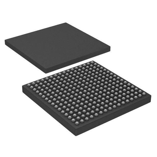
| 描述 | IC FPGA 63 I/O 100VQFP |
| 产品分类 | |
| I/O数 | 63 |
| LAB/CLB数 | 192 |
| 品牌 | Xilinx Inc |
| 数据手册 | |
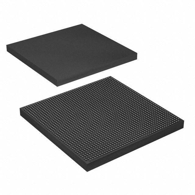
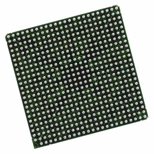
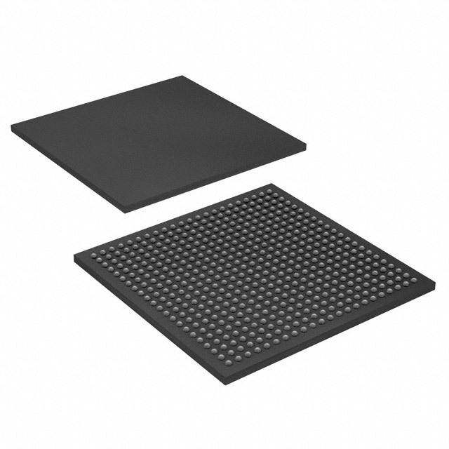
| 产品图片 |
|
| 产品型号 | XC3S50-4VQG100C |
| rohs | 无铅 / 符合限制有害物质指令(RoHS)规范要求 |
| 产品系列 | Spartan®-3 |
| 产品培训模块 | http://www.digikey.cn/PTM/IndividualPTM.page?site=cn&lang=zhs&ptm=4790 |
| 产品目录页面 | |
| 供应商器件封装 | 100-VQFP(14x14) |
| 其它名称 | 122-1504 |
| 安装类型 | 表面贴装 |
| 封装/外壳 | 100-TQFP |
| 工作温度 | 0°C ~ 85°C |
| 总RAM位数 | 73728 |
| 栅极数 | 50000 |
| 标准包装 | 90 |
| 电压-电源 | 1.14 V ~ 1.26 V |
| 逻辑元件/单元数 | 1728 |


- 商务部:美国ITC正式对集成电路等产品启动337调查
- 曝三星4nm工艺存在良率问题 高通将骁龙8 Gen1或转产台积电
- 太阳诱电将投资9.5亿元在常州建新厂生产MLCC 预计2023年完工
- 英特尔发布欧洲新工厂建设计划 深化IDM 2.0 战略
- 台积电先进制程称霸业界 有大客户加持明年业绩稳了
- 达到5530亿美元!SIA预计今年全球半导体销售额将创下新高
- 英特尔拟将自动驾驶子公司Mobileye上市 估值或超500亿美元
- 三星加码芯片和SET,合并消费电子和移动部门,撤换高东真等 CEO
- 三星电子宣布重大人事变动 还合并消费电子和移动部门
- 海关总署:前11个月进口集成电路产品价值2.52万亿元 增长14.8%

PDF Datasheet 数据手册内容提取
1 Spartan-3 FPGA Family Data Sheet DS099 June 27, 2013 Product Specification Module 1: Module 4: Pinout Descriptions Introduction and Ordering Information DS099 (v3.1) June 27, 2013 DS099 (v3.1) June 27, 2013 (cid:129) Pin Descriptions (cid:129) Introduction (cid:129) Pin Behavior During Configuration (cid:129) Features (cid:129) Package Overview (cid:129) Architectural Overview (cid:129) Pinout Tables (cid:129) Array Sizes and Resources (cid:129) Footprints (cid:129) User I/O Chart (cid:129) Ordering Information Module 2: Functional Description DS099 (v3.1) June 27, 2013 (cid:129) Input/Output Blocks (IOBs) (cid:129) IOB Overview (cid:129) SelectIO™ Interface I/O Standards (cid:129) Configurable Logic Blocks (CLBs) (cid:129) Block RAM (cid:129) Dedicated Multipliers (cid:129) Digital Clock Manager (DCM) (cid:129) Clock Network (cid:129) Configuration Module 3: DC and Switching Characteristics DS099 (v3.1) June 27, 2013 (cid:129) DC Electrical Characteristics (cid:129) Absolute Maximum Ratings (cid:129) Supply Voltage Specifications (cid:129) Recommended Operating Conditions (cid:129) DC Characteristics (cid:129) Switching Characteristics (cid:129) I/O Timing (cid:129) Internal Logic Timing (cid:129) DCM Timing (cid:129) Configuration and JTAG Timing © Copyright 2003–2013 Xilinx, Inc. XILINX, the Xilinx logo, Virtex, Spartan, ISE, Artix, Kintex, Zynq, Vivado, and other designated brands included herein are trademarks of Xilinx in the United States and other countries. PCI and PCI-X are trademarks of PCI-SIG and used under license. All other trademarks are the property of their respective owners. DS099 June 27, 2013 www.xilinx.com Product Specification 1
8 Spartan-3 FPGA Family: Introduction and Ordering Information DS099 (v3.1) June 27, 2013 Product Specification Introduction Features (cid:129) Low-cost, high-performance logic solution for high-volume, The Spartan®-3 family of Field-Programmable Gate Arrays consumer-oriented applications is specifically designed to meet the needs of high volume, (cid:129) Densities up to 74,880 logic cells cost-sensitive consumer electronic applications. The (cid:129) SelectIO™ interface signaling eight-member family offers densities ranging from 50,000 to (cid:129) Up to 633 I/O pins 5,000,000 system gates, as shown in Table1. (cid:129) 622+ Mb/s data transfer rate per I/O (cid:129) 18 single-ended signal standards The Spartan-3 family builds on the success of the earlier (cid:129) 8 differential I/O standards including LVDS, RSDS Spartan-IIE family by increasing the amount of logic (cid:129) Termination by Digitally Controlled Impedance (cid:129) Signal swing ranging from 1.14V to 3.465V resources, the capacity of internal RAM, the total number of (cid:129) Double Data Rate (DDR) support I/Os, and the overall level of performance as well as by (cid:129) DDR, DDR2 SDRAM support up to 333Mb/s improving clock management functions. Numerous (cid:129) Logic resources enhancements derive from the Virtex®-II platform (cid:129) Abundant logic cells with shift register capability technology. These Spartan-3 FPGA enhancements, (cid:129) Wide, fast multiplexers (cid:129) Fast look-ahead carry logic combined with advanced process technology, deliver more (cid:129) Dedicated 18 x 18 multipliers functionality and bandwidth per dollar than was previously (cid:129) JTAG logic compatible with IEEE 1149.1/1532 possible, setting new standards in the programmable logic (cid:129) SelectRAM™ hierarchical memory industry. (cid:129) Up to 1,872 Kbits of total block RAM (cid:129) Up to 520 Kbits of total distributed RAM Because of their exceptionally low cost, Spartan-3 FPGAs (cid:129) Digital Clock Manager (up to four DCMs) are ideally suited to a wide range of consumer electronics (cid:129) Clock skew elimination applications, including broadband access, home (cid:129) Frequency synthesis networking, display/projection and digital television (cid:129) High resolution phase shifting equipment. (cid:129) Eight global clock lines and abundant routing (cid:129) Fully supported by Xilinx ISE® and WebPACK™ software The Spartan-3 family is a superior alternative to mask development systems programmed ASICs. FPGAs avoid the high initial cost, the (cid:129) MicroBlaze™ and PicoBlaze™ processor, PCI®, lengthy development cycles, and the inherent inflexibility of PCIExpress® PIPE Endpoint, and other IP cores conventional ASICs. Also, FPGA programmability permits (cid:129) Pb-free packaging options design upgrades in the field with no hardware replacement (cid:129) Automotive Spartan-3 XA Family variant necessary, an impossibility with ASICs. Table 1: Summary of Spartan-3 FPGA Attributes CLB Array System Equivalent (One CLB = Four Slices) Distributed Block Dedicated Max. Maximum Device RAM Bits RAM Bits DCMs Differential Gates Logic Cells(1) Total Multipliers User I/O Rows Columns (K=1024) (K=1024) I/O Pairs CLBs XC3S50(2) 50K 1,728 16 12 192 12K 72K 4 2 124 56 XC3S200(2) 200K 4,320 24 20 480 30K 216K 12 4 173 76 XC3S400(2) 400K 8,064 32 28 896 56K 288K 16 4 264 116 XC3S1000(2) 1M 17,280 48 40 1,920 120K 432K 24 4 391 175 XC3S1500 1.5M 29,952 64 52 3,328 208K 576K 32 4 487 221 XC3S2000 2M 46,080 80 64 5,120 320K 720K 40 4 565 270 XC3S4000 4M 62,208 96 72 6,912 432K 1,728K 96 4 633 300 XC3S5000 5M 74,880 104 80 8,320 520K 1,872K 104 4 633 300 Notes: 1. Logic Cell = 4-input Look-Up Table (LUT) plus a ‘D’ flip-flop. "Equivalent Logic Cells" equals "Total CLBs" x 8 Logic Cells/CLB x 1.125 effectiveness. 2. These devices are available in Xilinx Automotive versions as described in DS314: Spartan-3 Automotive XA FPGA Family. © Copyright 2003–2013 Xilinx, Inc. XILINX, the Xilinx logo, Virtex, Spartan, ISE, Artix, Kintex, Zynq, Vivado, and other designated brands included herein are trademarks of Xilinx in the United States and other countries. PCI and PCI-X are trademarks of PCI-SIG and used under license. All other trademarks are the property of their respective owners. DS099 (v3.1) June 27, 2013 www.xilinx.com Product Specification 2
Spartan-3 FPGA Family: Introduction and Ordering Information Architectural Overview The Spartan-3 family architecture consists of five fundamental programmable functional elements: (cid:129) Configurable Logic Blocks (CLBs) contain RAM-based Look-Up Tables (LUTs) to implement logic and storage elements that can be used as flip-flops or latches. CLBs can be programmed to perform a wide variety of logical functions as well as to store data. (cid:129) Input/Output Blocks (IOBs) control the flow of data between the I/O pins and the internal logic of the device. Each IOB supports bidirectional data flow plus 3-state operation. Twenty-six different signal standards, including eight high-performance differential standards, are available as shown in Table2. Double Data-Rate (DDR) registers are included. The Digitally Controlled Impedance (DCI) feature provides automatic on-chip terminations, simplifying board designs. (cid:129) Block RAM provides data storage in the form of 18-Kbit dual-port blocks. (cid:129) Multiplier blocks accept two 18-bit binary numbers as inputs and calculate the product. (cid:129) Digital Clock Manager (DCM) blocks provide self-calibrating, fully digital solutions for distributing, delaying, multiplying, dividing, and phase shifting clock signals. These elements are organized as shown in Figure1. A ring of IOBs surrounds a regular array of CLBs. The XC3S50 has a single column of block RAM embedded in the array. Those devices ranging from the XC3S200 to the XC3S2000 have two columns of block RAM. The XC3S4000 and XC3S5000 devices have four RAM columns. Each column is made up of several 18-Kbit RAM blocks; each block is associated with a dedicated multiplier. The DCMs are positioned at the ends of the outer block RAM columns. The Spartan-3 family features a rich network of traces and switches that interconnect all five functional elements, transmitting signals among them. Each functional element has an associated switch matrix that permits multiple connections to the routing. X-Ref Target - Figure 1 DS099-1_01_032703 Notes: 1. The two additional block RAM columns of the XC3S4000 and XC3S5000 devices are shown with dashed lines. The XC3S50 has only the block RAM column on the far left. Figure 1: Spartan-3 Family Architecture Configuration Spartan-3 FPGAs are programmed by loading configuration data into robust reprogrammable static CMOS configuration latches (CCLs) that collectively control all functional elements and routing resources. Before powering on the FPGA, configuration data is stored externally in a PROM or some other nonvolatile medium either on or off the board. After applying DS099 (v3.1) June 27, 2013 www.xilinx.com Product Specification 3
Spartan-3 FPGA Family: Introduction and Ordering Information power, the configuration data is written to the FPGA using any of five different modes: Master Parallel, Slave Parallel, Master Serial, Slave Serial, and Boundary Scan (JTAG). The Master and Slave Parallel modes use an 8-bit-wide SelectMAP port. The recommended memory for storing the configuration data is the low-cost Xilinx Platform Flash PROM family, which includes the XCF00S PROMs for serial configuration and the higher density XCF00P PROMs for parallel or serial configuration. I/O Capabilities The SelectIO feature of Spartan-3 devices supports eighteen single-ended standards and eight differential standards as listed in Table2. Many standards support the DCI feature, which uses integrated terminations to eliminate unwanted signal reflections. Table 2: Signal Standards Supported by the Spartan-3 Family Standard Symbol DCI Description V (V) Class Category CCO (IOSTANDARD) Option Single-Ended GTL Gunning Transceiver Logic N/A Terminated GTL Yes Plus GTLP Yes HSTL High-Speed Transceiver Logic 1.5 I HSTL_I Yes III HSTL_III Yes 1.8 I HSTL_I_18 Yes II HSTL_II_18 Yes III HSTL_III_18 Yes LVCMOS Low-Voltage CMOS 1.2 N/A LVCMOS12 No 1.5 N/A LVCMOS15 Yes 1.8 N/A LVCMOS18 Yes 2.5 N/A LVCMOS25 Yes 3.3 N/A LVCMOS33 Yes LVTTL Low-Voltage Transistor-Transistor Logic 3.3 N/A LVTTL No PCI Peripheral Component Interconnect 3.0 33MHz(1) PCI33_3 No SSTL Stub Series Terminated Logic 1.8 N/A (±6.7 mA) SSTL18_I Yes N/A (±13.4 mA) SSTL18_II No 2.5 I SSTL2_I Yes II SSTL2_II Yes Differential LDT Lightning Data Transport (HyperTransport™) 2.5 N/A LDT_25 No (ULVDS) Logic LVDS Low-Voltage Differential Signaling Standard LVDS_25 Yes Bus BLVDS_25 No Extended Mode LVDSEXT_25 Yes LVPECL Low-Voltage Positive Emitter-Coupled Logic 2.5 N/A LVPECL_25 No RSDS Reduced-Swing Differential Signaling 2.5 N/A RSDS_25 No HSTL Differential High-Speed Transceiver Logic 1.8 II DIFF_HSTL_II_18 Yes SSTL Differential Stub Series Terminated Logic 2.5 II DIFF_SSTL2_II Yes Notes: 1. 66 MHz PCI is not supported by the Xilinx IP core although PCI66_3 is an available I/O standard. DS099 (v3.1) June 27, 2013 www.xilinx.com Product Specification 4
Spartan-3 FPGA Family: Introduction and Ordering Information Table3 shows the number of user I/Os as well as the number of differential I/O pairs available for each device/package combination. Table 3: Spartan-3 Device I/O Chart Available User I/Os and Differential (Diff) I/O Pairs by Package Type VQ100 CP132(1) TQ144 PQ208 FT256 FG320 FG456 FG676 FG900 FG1156(1) Package VQG100 CPG132 TQG144 PQG208 FTG256 FGG320 FGG456 FGG676 FGG900 FGG1156 Footprint 16x16 8x8 22x22 30.6x30.6 17x17 19x19 23x23 27x27 31x31 35x35 (mm) Device User Diff User Diff User Diff User Diff User Diff User Diff User Diff User Diff User Diff User Diff XC3S50 63 29 89(1) 44(1) 97 46 124 56 – – – – – – – – – – – – XC3S200 63 29 – – 97 46 141 62 173 76 – – – – – – – – – – XC3S400 – – – – 97 46 141 62 173 76 221 100 264 116 – – – – – – XC3S1000 – – – – – – – – 173 76 221 100 333 149 391 175 – – – – XC3S1500 – – – – – – – – – – 221 100 333 149 487 221 – – – – XC3S2000 – – – – – – – – – – – – 333 149 489 221 565 270 – – XC3S4000 – – – – – – – – – – – – – – 489 221 633 300 712(1) 312(1) XC3S5000 – – – – – – – – – – – – – – 489 221 633 300 784(1) 344(1) Notes: 1. The CP132, CPG132, FG1156, and FGG1156 packages are discontinued. See http://www.xilinx.com/support/documentation/spartan-3_customer_notices.htm. 2. All device options listed in a given package column are pin-compatible. 3. User = Single-ended user I/O pins. Diff = Differential I/O pairs. Package Marking Figure2 shows the top marking for Spartan-3 FPGAs in the quad-flat packages. Figure3 shows the top marking for Spartan-3 FPGAs in BGA packages except the 132-ball chip-scale package (CP132 and CPG132). The markings for the BGA packages are nearly identical to those for the quad-flat packages, except that the marking is rotated with respect to the ball A1 indicator. Figure4 shows the top marking for Spartan-3 FPGAs in the CP132 and CPG132 packages. The “5C” and “4I” part combinations may be dual marked as “5C/4I”. Devices with the dual mark can be used as either -5C or -4I devices. Devices with a single mark are only guaranteed for the marked speed grade and temperature range. Some specifications vary according to mask revision. Mask revision E devices are errata-free. All shipments since 2006 have been mask revision E. X-Ref Target - Figure 2 Mask Revision Code Fabrication Code R SPARTANR Process Technology Device Type XC3S400 TM Package PQ208EGQ0525 Date Code D1234567A Lot Code Speed Grade 4C Temperature Range Pin P1 DS099-1_03_050305 Figure 2: Spartan-3 FPGA QFP Package Marking Example for Part Number XC3S400-4PQ208C DS099 (v3.1) June 27, 2013 www.xilinx.com Product Specification 5
Spartan-3 FPGA Family: Introduction and Ordering Information X-Ref Target - Figure 3 Mask Revision Code BGA Ball A1 R Fabrication Code SPARTANR Process Code Device Type XC3S1000TM Package FT256EGQ0525 Date Code D1234567A Lot Code 4C Speed Grade Temperature Range DS099-1_04_050305 Figure 3: Spartan-3 FPGA BGA Package Marking Example for Part Number XC3S1000-4FT256C X-Ref Target - Figure 4 Ball A1 3S50 Device Type Lot Code F12345 -0525 Date Code PHILIPPINES Temperature Range Package C5-EGQ 4C C5 = CP132 C6 = CPG132 Speed Grade Process Code Mask Revision Code Fabrication Code DS099-1_05_092712 Figure 4: Spartan-3 FPGA CP132 and CPG132 Package Marking Example for XC3S50-4CP132C Ordering Information Spartan-3 FPGAs are available in both standard (Figure5) and Pb-free (Figure6) packaging options for all device/package combinations. The Pb-free packages include a special ‘G’ character in the ordering code. X-Ref Target - Figure 5 Example:XC3S50 -4 PQ 208 C Device Type Temperature Range: C = Commercial (T = 0°C to 85°C) j Speed Grade I = Industrial (T = –40°C to +100°C) j Package Type Number of Pins DS099_1_05_020711 Figure 5: Standard Packaging For additional information on Pb-free packaging, see XAPP427: Implementation and Solder Reflow Guidelines for Pb-Free Packages. X-Ref Target - Figure 6 Example: XC3S50 -4 PQ G 208 C Device Type Temperature Range: C = Commercial (T = 0°C to 85°C) j Speed Grade I = Industrial (T = –40°C to +100°C) j Number of Pins Package Type Pb-free DS099_1_06_020711 Figure 6: Pb-Free Packaging DS099 (v3.1) June 27, 2013 www.xilinx.com Product Specification 6
Spartan-3 FPGA Family: Introduction and Ordering Information Table 4: Example Ordering Information Device Speed Grade Package Type/Number of Pins Temperature Range (T) j XC3S50 -4 Standard Performance VQ(G)100 100-pin Very Thin Quad Flat Pack (VQFP) C Commercial (0°C to 85°C) XC3S200 -5 High Performance(1) CP(G)132(2) 132-pin Chip-Scale Package (CSP) I Industrial (–40°C to 100°C) XC3S400 TQ(G)144 144-pin Thin Quad Flat Pack (TQFP) XC3S1000 PQ(G)208 208-pin Plastic Quad Flat Pack (PQFP) XC3S1500 FT(G)256 256-ball Fine-Pitch Thin Ball Grid Array (FTBGA) XC3S2000 FG(G)320 320-ball Fine-Pitch Ball Grid Array (FBGA) XC3S4000 FG(G)456 456-ball Fine-Pitch Ball Grid Array (FBGA) XC3S5000 FG(G)676 676-ball Fine-Pitch Ball Grid Array (FBGA) FG(G)900 900-ball Fine-Pitch Ball Grid Array (FBGA) FG(G)1156(2) 1156-ball Fine-Pitch Ball Grid Array (FBGA) Notes: 1. The -5 speed grade is exclusively available in the Commercial temperature range. 2. The CP132, CPG132, FG1156, and FGG1156 packages are discontinued. See http://www.xilinx.com/support/documentation/spartan-3_customer_notices.htm. Revision History Date Version Description 04/11/2003 1.0 Initial Xilinx release. 04/24/2003 1.1 Updated block RAM, DCM, and multiplier counts for the XC3S50. 12/24/2003 1.2 Added the FG320 package. 07/13/2004 1.3 Added information on Pb-free packaging options. 01/17/2005 1.4 Referenced Spartan-3 XA Automotive FPGA families in Table1. Added XC3S50CP132, XC3S2000FG456, XC3S4000FG676 options to Table3. Updated Package Marking to show mask revision code, fabrication facility code, and process technology code. 08/19/2005 1.5 Added package markings for BGA packages (Figure3) and CP132/CPG132 packages (Figure4). Added differential (complementary single-ended) HSTL and SSTL I/O standards. 04/03/2006 2.0 Increased number of supported single-ended and differential I/O standards. 04/26/2006 2.1 Updated document links. 05/25/2007 2.2 Updated Package Marking to allow for dual-marking. 11/30/2007 2.3 Added XC3S5000 FG(G)676 to Table3. Noted that FG(G)1156 package is being discontinued and updated max I/O count. 06/25/2008 2.4 Updated max I/O counts based on FG1156 discontinuation. Clarified dual mark in Package Marking. Updated formatting and links. 12/04/2009 2.5 CP132 and CPG132 packages are being discontinued. Added link to Spartan-3 FPGA customer notices. Updated Table3 with package footprint dimensions. 10/29/2012 3.0 Added Notice of Disclaimer section. Per XCN07022, updated the discontinued FG1156 and FGG1156 package discussion throughout document. Per XCN08011, updated the discontinued CP132 and CPG132 package discussion throughout document. Although the package is discontinued, updated the marking on Figure4. This product is not recommended for new designs. 06/27/2013 3.1 Removed banner. This product IS recommended for new designs. DS099 (v3.1) June 27, 2013 www.xilinx.com Product Specification 7
Spartan-3 FPGA Family: Introduction and Ordering Information Notice of Disclaimer THE XILINX HARDWARE FPGA AND CPLD DEVICES REFERRED TO HEREIN (“PRODUCTS”) ARE SUBJECT TO THE TERMS AND CONDITIONS OF THE XILINX LIMITED WARRANTY WHICH CAN BE VIEWED AT http://www.xilinx.com/warranty.htm. THIS LIMITED WARRANTY DOES NOT EXTEND TO ANY USE OF PRODUCTS IN AN APPLICATION OR ENVIRONMENT THAT IS NOT WITHIN THE SPECIFICATIONS STATED IN THE XILINX DATA SHEET. ALL SPECIFICATIONS ARE SUBJECT TO CHANGE WITHOUT NOTICE. PRODUCTS ARE NOT DESIGNED OR INTENDED TO BE FAIL-SAFE OR FOR USE IN ANY APPLICATION REQUIRING FAIL-SAFE PERFORMANCE, SUCH AS LIFE-SUPPORT OR SAFETY DEVICES OR SYSTEMS, OR ANY OTHER APPLICATION THAT INVOKES THE POTENTIAL RISKS OF DEATH, PERSONAL INJURY, OR PROPERTY OR ENVIRONMENTAL DAMAGE (“CRITICAL APPLICATIONS”). USE OF PRODUCTS IN CRITICAL APPLICATIONS IS AT THE SOLE RISK OF CUSTOMER, SUBJECT TO APPLICABLE LAWS AND REGULATIONS. CRITICAL APPLICATIONS DISCLAIMER XILINX PRODUCTS (INCLUDING HARDWARE, SOFTWARE AND/OR IP CORES) ARE NOT DESIGNED OR INTENDED TO BE FAIL-SAFE, OR FOR USE IN ANY APPLICATION REQUIRING FAIL-SAFE PERFORMANCE, SUCH AS IN LIFE-SUPPORT OR SAFETY DEVICES OR SYSTEMS, CLASS III MEDICAL DEVICES, NUCLEAR FACILITIES, APPLICATIONS RELATED TO THE DEPLOYMENT OF AIRBAGS, OR ANY OTHER APPLICATIONS THAT COULD LEAD TO DEATH, PERSONAL INJURY OR SEVERE PROPERTY OR ENVIRONMENTAL DAMAGE (INDIVIDUALLY AND COLLECTIVELY, “CRITICAL APPLICATIONS”). FURTHERMORE, XILINX PRODUCTS ARE NOT DESIGNED OR INTENDED FOR USE IN ANY APPLICATIONS THAT AFFECT CONTROL OF A VEHICLE OR AIRCRAFT, UNLESS THERE IS A FAIL-SAFE OR REDUNDANCY FEATURE (WHICH DOES NOT INCLUDE USE OF SOFTWARE IN THE XILINX DEVICE TO IMPLEMENT THE REDUNDANCY) AND A WARNING SIGNAL UPON FAILURE TO THE OPERATOR. CUSTOMER AGREES, PRIOR TO USING OR DISTRIBUTING ANY SYSTEMS THAT INCORPORATE XILINX PRODUCTS, TO THOROUGHLY TEST THE SAME FOR SAFETY PURPOSES. TO THE MAXIMUM EXTENT PERMITTED BY APPLICABLE LAW, CUSTOMER ASSUMES THE SOLE RISK AND LIABILITY OF ANY USE OF XILINX PRODUCTS IN CRITICAL APPLICATIONS. AUTOMOTIVE APPLICATIONS DISCLAIMER XILINX PRODUCTS ARE NOT DESIGNED OR INTENDED TO BE FAIL-SAFE, OR FOR USE IN ANY APPLICATION REQUIRING FAIL-SAFE PERFORMANCE, SUCH AS APPLICATIONS RELATED TO: (I) THE DEPLOYMENT OF AIRBAGS, (II) CONTROL OF A VEHICLE, UNLESS THERE IS A FAIL-SAFE OR REDUNDANCY FEATURE (WHICH DOES NOT INCLUDE USE OF SOFTWARE IN THE XILINX DEVICE TO IMPLEMENT THE REDUNDANCY) AND A WARNING SIGNAL UPON FAILURE TO THE OPERATOR, OR (III) USES THAT COULD LEAD TO DEATH OR PERSONAL INJURY. CUSTOMER ASSUMES THE SOLE RISK AND LIABILITY OF ANY USE OF XILINX PRODUCTS IN SUCH APPLICATIONS. DS099 (v3.1) June 27, 2013 www.xilinx.com Product Specification 8
57 Spartan-3 FPGA Family: Functional Description DS099 (v3.1) June 27, 2013 Product Specification Spartan-3 FPGA Design Documentation The functionality of the Spartan®-3 FPGA family is described in the following documents. The topics covered in each guide are listed. (cid:129) UG331: Spartan-3 Generation FPGA User Guide Create a Xilinx user account and sign up to receive automatic e-mail notification whenever this data sheet or (cid:129) Clocking Resources the associated user guides are updated. (cid:129) Digital Clock Managers (DCMs) (cid:129) Sign Up for Alerts on Xilinx.com (cid:129) Block RAM https://secure.xilinx.com/webreg/register.do (cid:129) Configurable Logic Blocks (CLBs) ?group=myprofile&languageID=1 - Distributed RAM For specific hardware examples, see the Spartan-3 FPGA - SRL16 Shift Registers Starter Kit board web page, which has links to various design examples and the user guide. - Carry and Arithmetic Logic (cid:129) I/O Resources (cid:129) Spartan-3 FPGA Starter Kit Board page http://www.xilinx.com/s3starter (cid:129) Embedded Multiplier Blocks (cid:129) UG130: Spartan-3 FPGA Starter Kit User Guide (cid:129) Programmable Interconnect (cid:129) ISE® Software Design Tools (cid:129) IP Cores (cid:129) Embedded Processing and Control Solutions (cid:129) Pin Types and Package Overview (cid:129) Package Drawings (cid:129) Powering FPGAs (cid:129) UG332: Spartan-3 Generation Configuration User Guide (cid:129) Configuration Overview - Configuration Pins and Behavior - Bitstream Sizes (cid:129) Detailed Descriptions by Mode - Master Serial Mode using Xilinx Platform Flash PROM - Slave Parallel (SelectMAP) using a Processor - Slave Serial using a Processor - JTAG Mode (cid:129) ISE iMPACT Programming Examples © Copyright 2003–2013 Xilinx, Inc. XILINX, the Xilinx logo, Virtex, Spartan, ISE, Artix, Kintex, Zynq, Vivado, and other designated brands included herein are trademarks of Xilinx in the United States and other countries. PCI and PCI-X are trademarks of PCI-SIG and used under license. All other trademarks are the property of their respective owners. DS099 (v3.1) June 27, 2013 www.xilinx.com Product Specification 9
Spartan-3 FPGA Family: Functional Description IOBs For additional information, refer to the chapter entitled “Using I/O Resources” in UG331: Spartan-3 Generation FPGA User Guide. IOB Overview The Input/Output Block (IOB) provides a programmable, bidirectional interface between an I/O pin and the FPGA’s internal logic. A simplified diagram of the IOB’s internal structure appears in Figure7. There are three main signal paths within the IOB: the output path, input path, and 3-state path. Each path has its own pair of storage elements that can act as either registers or latches. For more information, see the Storage Element Functions section. The three main signal paths are as follows: (cid:129) The input path carries data from the pad, which is bonded to a package pin, through an optional programmable delay element directly to the I line. There are alternate routes through a pair of storage elements to the IQ1 and IQ2 lines. The IOB outputs I, IQ1, and IQ2 all lead to the FPGA’s internal logic. The delay element can be set to ensure a hold time of zero. (cid:129) The output path, starting with the O1 and O2 lines, carries data from the FPGA’s internal logic through a multiplexer and then a three-state driver to the IOB pad. In addition to this direct path, the multiplexer provides the option to insert a pair of storage elements. (cid:129) The 3-state path determines when the output driver is high impedance. The T1 and T2 lines carry data from the FPGA’s internal logic through a multiplexer to the output driver. In addition to this direct path, the multiplexer provides the option to insert a pair of storage elements. When the T1 or T2 lines are asserted High, the output driver is high-impedance (floating, hi-Z). The output driver is active-Low enabled. (cid:129) All signal paths entering the IOB, including those associated with the storage elements, have an inverter option. Any inverter placed on these paths is automatically absorbed into the IOB. Storage Element Functions There are three pairs of storage elements in each IOB, one pair for each of the three paths. It is possible to configure each of these storage elements as an edge-triggered D-type flip-flop (FD) or a level-sensitive latch (LD). The storage-element-pair on either the Output path or the Three-State path can be used together with a special multiplexer to produce Double-Data-Rate (DDR) transmission. This is accomplished by taking data synchronized to the clock signal’s rising edge and converting them to bits synchronized on both the rising and the falling edge. The combination of two registers and a multiplexer is referred to as a Double-Data-Rate D-type flip-flop (FDDR). See Double-Data-Rate Transmission, page12 for more information. The signal paths associated with the storage element are described in Table5. Table 5: Storage Element Signal Description Storage Element Description Function Signal D Data input Data at this input is stored on the active edge of CK enabled by CE. For latch operation when the input is enabled, data passes directly to the output Q. Q Data output The data on this output reflects the state of the storage element. For operation as a latch in transparent mode, Q will mirror the data at D. CK Clock input A signal’s active edge on this input with CE asserted, loads data into the storage element. CE Clock Enable input When asserted, this input enables CK. If not connected, CE defaults to the asserted state. SR Set/Reset Forces storage element into the state specified by the SRHIGH/SRLOW attributes. The SYNC/ASYNC attribute setting determines if the SR input is synchronized to the clock or not. REV Reverse Used together with SR. Forces storage element into the state opposite from what SR does. DS099 (v3.1) June 27, 2013 www.xilinx.com Product Specification 10
Spartan-3 FPGA Family: Functional Description X-Ref Target - Figure 7 T TFF1 T1 D Q CE CK SR REV DDR MUX TCE T2 D Q TFF2 CE CK SR REV Three-state Path OFF1 VCCO O1 D Q CE Pull-Up ESD OTCLK1 CK SR REV DDR I/O MUX Pin OCE Program- Pull- O2 D Q mable Down ESD OFF2 Output DCI Driver CE OTCLK2 CK SR REV Keeper Latch Output Path I Fixed IQ1 Delay LVCMOS, LVTTL, PCI D Q IFF1 Fixed Single-ended Standards CE Delay using VREF ICLK1 CK VPiRnEF ICE SR REV Differential Standards IQ2 I/O Pin from D Q Adjacent IFF2 IOB CE ICLK2 CK SR REV SR REV Input Path Note: All IOB signals originating from the FPGA's internal logic have an optional polarity inverter. DS099-2_01_091410 Figure 7: Simplified IOB Diagram DS099 (v3.1) June 27, 2013 www.xilinx.com Product Specification 11
Spartan-3 FPGA Family: Functional Description According to Figure7, the clock line OTCLK1 connects the CK inputs of the upper registers on the output and three-state paths. Similarly, OTCLK2 connects the CK inputs for the lower registers on the output and three-state paths. The upper and lower registers on the input path have independent clock lines: ICLK1 and ICLK2. The enable line OCE connects the CE inputs of the upper and lower registers on the output path. Similarly, TCE connects the CE inputs for the register pair on the three-state path and ICE does the same for the register pair on the input path. The Set/Reset (SR) line entering the IOB is common to all six registers, as is the Reverse (REV) line. Each storage element supports numerous options in addition to the control over signal polarity described in the IOB Overview section. These are described in Table6. Table 6: Storage Element Options Option Switch Function Specificity FF/Latch Chooses between an edge-sensitive flip-flop or a Independent for each storage element. level-sensitive latch SYNC/ASYNC Determines whether SR is synchronous or Independent for each storage element. asynchronous SRHIGH/SRLOW Determines whether SR acts as a Set, which forces the Independent for each storage element, except when using storage element to a logic “1" (SRHIGH) or a Reset, FDDR. In the latter case, the selection for the upper which forces a logic “0” (SRLOW). element (OFF1 or TFF2) applies to both elements. INIT1/INIT0 In the event of a Global Set/Reset, after configuration Independent for each storage element, except when using or upon activation of the GSR net, this switch decides FDDR. In the latter case, selecting INIT0 for one element whether to set or reset a storage element. By default, applies to both elements (even though INIT1 is selected choosing SRLOW also selects INIT0; choosing for the other). SRHIGH also selects INIT1. Double-Data-Rate Transmission Double-Data-Rate (DDR) transmission describes the technique of synchronizing signals to both the rising and falling edges of the clock signal. Spartan-3 devices use register-pairs in all three IOB paths to perform DDR operations. The pair of storage elements on the IOB’s Output path (OFF1 and OFF2), used as registers, combine with a special multiplexer to form a DDR D-type flip-flop (FDDR). This primitive permits DDR transmission where output data bits are synchronized to both the rising and falling edges of a clock. It is possible to access this function by placing either an FDDRRSE or an FDDRCPE component or symbol into the design. DDR operation requires two clock signals (50% duty cycle), one the inverted form of the other. These signals trigger the two registers in alternating fashion, as shown in Figure8. Commonly, the Digital Clock Manager (DCM) generates the two clock signals by mirroring an incoming signal, then shifting it 180 degrees. This approach ensures minimal skew between the two signals. The storage-element-pair on the Three-State path (TFF1 and TFF2) can also be combined with a local multiplexer to form an FDDR primitive. This permits synchronizing the output enable to both the rising and falling edges of a clock. This DDR operation is realized in the same way as for the output path. The storage-element-pair on the input path (IFF1 and IFF2) allows an I/O to receive a DDR signal. An incoming DDR clock signal triggers one register and the inverted clock signal triggers the other register. In this way, the registers take turns capturing bits of the incoming DDR data signal. DS099 (v3.1) June 27, 2013 www.xilinx.com Product Specification 12
Spartan-3 FPGA Family: Functional Description X-Ref Target - Figure 8 DCM 180˚0˚ FDDR D1 Q1 CLK1 DDR MUX Q D2 Q2 CLK2 DS099-2_02_070303 Figure 8: Clocking the DDR Register Aside from high bandwidth data transfers, DDR can also be used to reproduce, or “mirror”, a clock signal on the output. This approach is used to transmit clock and data signals together. A similar approach is used to reproduce a clock signal at multiple outputs. The advantage for both approaches is that skew across the outputs will be minimal. Some adjacent I/O blocks (IOBs) share common routing connecting the ICLK1, ICLK2, OTCLK1, and OTCLK2 clock inputs of both IOBs. These IOB pairs are identified by their differential pair names IO_LxxN_# and IO_LxxP_#, where "xx" is an I/O pair number and ‘#’ is an I/O bank number. Two adjacent IOBs containing DDR registers must share common clock inputs, otherwise one or more of the clock signals will be unroutable. Pull-Up and Pull-Down Resistors The optional pull-up and pull-down resistors are intended to establish High and Low levels, respectively, at unused I/Os. The pull-up resistor optionally connects each IOB pad to V . A pull-down resistor optionally connects each pad to GND. These CCO resistors are placed in a design using the PULLUP and PULLDOWN symbols in a schematic, respectively. They can also be instantiated as components, set as constraints or passed as attributes in HDL code. These resistors can also be selected for all unused I/O using the Bitstream Generator (BitGen) option UnusedPin. A Low logic level on HSWAP_EN activates the pull-up resistors on all I/Os during configuration (see The I/Os During Power-On, Configuration, and User Mode, page21). The Spartan-3 FPGAs I/O pull-up and pull-down resistors are significantly stronger than the "weak" pull-up/pull-down resistors used in previous Xilinx FPGA families. See Table33, page61 for equivalent resistor strengths. Keeper Circuit Each I/O has an optional keeper circuit that retains the last logic level on a line after all drivers have been turned off. This is useful to keep bus lines from floating when all connected drivers are in a high-impedance state. This function is placed in a design using the KEEPER symbol. Pull-up and pull-down resistors override the keeper circuit. DS099 (v3.1) June 27, 2013 www.xilinx.com Product Specification 13
Spartan-3 FPGA Family: Functional Description ESD Protection Clamp diodes protect all device pads against damage from Electro-Static Discharge (ESD) as well as excessive voltage transients. Each I/O has two clamp diodes: One diode extends P-to-N from the pad to V and a second diode extends CCO N-to-P from the pad to GND. During operation, these diodes are normally biased in the off state. These clamp diodes are always connected to the pad, regardless of the signal standard selected. The presence of diodes limits the ability of Spartan-3 FPGA I/Os to tolerate high signal voltages. The V absolute maximum rating in Table28, page58 specifies the IN voltage range that I/Os can tolerate. Slew Rate Control and Drive Strength Two options, FAST and SLOW, control the output slew rate. The FAST option supports output switching at a high rate. The SLOW option reduces bus transients. These options are only available when using one of the LVCMOS or LVTTL standards, which also provide up to seven different levels of current drive strength: 2, 4, 6, 8, 12, 16, and 24mA. Choosing the appropriate drive strength level is yet another means to minimize bus transients. Table7 shows the drive strengths that the LVCMOS and LVTTL standards support. Table 7: Programmable Output Drive Current Signal Standard Current Drive (mA) (IOSTANDARD) 2 4 6 8 12 16 24 LVTTL ✓ ✓ ✓ ✓ ✓ ✓ ✓ LVCMOS33 ✓ ✓ ✓ ✓ ✓ ✓ ✓ LVCMOS25 ✓ ✓ ✓ ✓ ✓ ✓ ✓ LVCMOS18 ✓ ✓ ✓ ✓ ✓ ✓ – LVCMOS15 ✓ ✓ ✓ ✓ ✓ – – LVCMOS12 ✓ ✓ ✓ – – – – Boundary-Scan Capability All Spartan-3 FPGA IOBs support boundary-scan testing compatible with IEEE 1149.1 standards. During boundary- scan operations such as EXTEST and HIGHZ the I/O pull-down resistor is active. For more information, see Boundary-Scan (JTAG) Mode, page50, and refer to the “Using Boundary-Scan and BSDL Files” chapter in UG331. SelectIO Interface Signal Standards The IOBs support 18 different single-ended signal standards, as listed in Table8. Furthermore, the majority of IOBs can be used in specific pairs supporting any of eight differential signal standards, as shown in Table9. To define the SelectIO™ interface signaling standard in a design, set the IOSTANDARD attribute to the appropriate setting. Xilinx provides a variety of different methods for applying the IOSTANDARD for maximum flexibility. For a full description of different methods of applying attributes to control IOSTANDARD, refer to the “Using I/O Resources” chapter in UG331. Together with placing the appropriate I/O symbol, two externally applied voltage levels, V and V , select the desired CCO REF signal standard. The V lines provide current to the output driver. The voltage on these lines determines the output CCO voltage swing for all standards except GTL and GTLP. All single-ended standards except the LVCMOS, LVTTL, and PCI varieties require a Reference Voltage (V ) to bias the REF input-switching threshold. Once a configuration data file is loaded into the FPGA that calls for the I/Os of a given bank to use such a signal standard, a few specifically reserved I/O pins on the same bank automatically convert to V inputs. When REF using one of the LVCMOS standards, these pins remain I/Os because the V voltage biases the input-switching CCO threshold, so there is no need for V . Select the V and V levels to suit the desired single-ended standard according REF CCO REF to Table8. DS099 (v3.1) June 27, 2013 www.xilinx.com Product Specification 14
Spartan-3 FPGA Family: Functional Description Table 8: Single-Ended I/O Standards V (Volts) Signal Standard CCO V for Inputs Board Termination REF (IOSTANDARD) (Volts)(1) Voltage (V ) in Volts For Outputs For Inputs TT GTL Note 2 Note 2 0.8 1.2 GTLP Note 2 Note 2 1 1.5 HSTL_I 1.5 – 0.75 0.75 HSTL_III 1.5 – 0.9 1.5 HSTL_I_18 1.8 – 0.9 0.9 HSTL_II_18 1.8 – 0.9 0.9 HSTL_III_18 1.8 – 1.1 1.8 LVCMOS12 1.2 1.2 – – LVCMOS15 1.5 1.5 – – LVCMOS18 1.8 1.8 – – LVCMOS25 2.5 2.5 – – LVCMOS33 3.3 3.3 – – LVTTL 3.3 3.3 – – PCI33_3 3.0 3.0 – – SSTL18_I 1.8 – 0.9 0.9 SSTL18_II 1.8 – 0.9 0.9 SSTL2_I 2.5 – 1.25 1.25 SSTL2_II 2.5 – 1.25 1.25 Notes: 1. Banks 4 and 5 of any Spartan-3 device in a VQ100 package do not support signal standards using V . REF 2. The V level used for the GTL and GTLP standards must be no lower than the termination voltage (V ), nor can it be lower than the CCO TT voltage at the I/O pad. 3. See Table10 for a listing of the single-ended DCI standards. Differential standards employ a pair of signals, one the opposite polarity of the other. The noise canceling (e.g., Common-Mode Rejection) properties of these standards permit exceptionally high data transfer rates. This section introduces the differential signaling capabilities of Spartan-3 devices. Each device-package combination designates specific I/O pairs that are specially optimized to support differential standards. A unique “L-number”, part of the pin name, identifies the line-pairs associated with each bank (see Figure40, page112). For each pair, the letters ‘P’ and ‘N’ designate the true and inverted lines, respectively. For example, the pin names IO_L43P_7 and IO_L43N_7 indicate the true and inverted lines comprising the line pair L43 on Bank 7. The V CCO lines provide current to the outputs. The V lines supply power to the differential inputs, making them independent of CCAUX the V voltage for an I/O bank. The V lines are not used. Select the V level to suit the desired differential standard CCO REF CCO according to Table9. DS099 (v3.1) June 27, 2013 www.xilinx.com Product Specification 15
Spartan-3 FPGA Family: Functional Description Table 9: Differential I/O Standards Signal Standard VCCO (Volts) V for Inputs (Volts) (IOSTANDARD) For Outputs For Inputs REF LDT_25 (ULVDS_25) 2.5 – – LVDS_25 2.5 – – BLVDS_25 2.5 – – LVDSEXT_25 2.5 – – LVPECL_25 2.5 – – RSDS_25 2.5 – – DIFF_HSTL_II_18 1.8 – – DIFF_SSTL2_II 2.5 – – Notes: 1. See Table10 for a listing of the differential DCI standards. The need to supply V and V imposes constraints on which standards can be used in the same bank. See The REF CCO Organization of IOBs into Banks section for additional guidelines concerning the use of the V and V lines. CCO REF Digitally Controlled Impedance (DCI) When the round-trip delay of an output signal—i.e., from output to input and back again—exceeds rise and fall times, it is common practice to add termination resistors to the line carrying the signal. These resistors effectively match the impedance of a device’s I/O to the characteristic impedance of the transmission line, thereby preventing reflections that adversely affect signal integrity. However, with the high I/O counts supported by modern devices, adding resistors requires significantly more components and board area. Furthermore, for some packages—e.g., ball grid arrays—it may not always be possible to place resistors close to pins. DCI answers these concerns by providing two kinds of on-chip terminations: Parallel terminations make use of an integrated resistor network. Series terminations result from controlling the impedance of output drivers. DCI actively adjusts both parallel and series terminations to accurately match the characteristic impedance of the transmission line. This adjustment process compensates for differences in I/O impedance that can result from normal variation in the ambient temperature, the supply voltage and the manufacturing process. When the output driver turns off, the series termination, by definition, approaches a very high impedance; in contrast, parallel termination resistors remain at the targeted values. DCI is available only for certain I/O standards, as listed in Table10. DCI is selected by applying the appropriate I/O standard extensions to symbols or components. There are five basic ways to configure terminations, as shown in Table11. The DCI I/O standard determines which of these terminations is put into effect. HSTL_I_DCI-, HSTL_III_DCI-, and SSTL2_I_DCI-type outputs do not require the VRN and VRP reference resistors. Likewise, LVDCI-type inputs do not require the VRN and VRP reference resistors. In a bank without any DCI I/O or a bank containing non-DCI I/O and purely HSTL_I_DCI- or HSTL_III_DCI-type outputs, or SSTL2_I_DCI-type outputs or LVDCI-type inputs, the associated VRN and VRP pins can be used as general-purpose I/O pins. The HSLVDCI (High-Speed LVDCI) standard is intended for bidirectional use. The driver is identical to LVDCI, while the input is identical to HSTL. By using a V -referenced input, HSLVDCI allows greater input sensitivity at the receiver than when REF using a single-ended LVCMOS-type receiver. DS099 (v3.1) June 27, 2013 www.xilinx.com Product Specification 16
Spartan-3 FPGA Family: Functional Description Table 10: DCI I/O Standards V (V) Termination Type Category of Signal Signal Standard CCO V for REF Standard (IOSTANDARD) Inputs (V) For Outputs For Inputs At Output At Input Single-Ended Gunning GTL_DCI 1.2 1.2 0.8 Transceiver Logic Single Single GTLP_DCI 1.5 1.5 1.0 High-Speed HSTL_I_DCI 1.5 1.5 0.75 None Split Transceiver Logic HSTL_III_DCI 1.5 1.5 0.9 None Single HSTL_I_DCI_18 1.8 1.8 0.9 None HSTL_II_DCI_18 Split 1.8 1.8 0.9 Split DIFF_HSTL_II_18_DCI HSTL_III_DCI_18 1.8 1.8 1.1 None Single Low-Voltage CMOS LVDCI_15 1.5 1.5 – LVDCI_18 1.8 1.8 – Controlled LVDCI_25 2.5 2.5 – impedance driver LVDCI_33(2) 3.3 3.3 – None LVDCI_DV2_15 1.5 1.5 – LVDCI_DV2_18 1.8 1.8 – Controlled driver with LVDCI_DV2_25 2.5 2.5 – half-impedance LVDCI_DV2_33 3.3 3.3 – Hybrid HSTL Input HSLVDCI_15 1.5 1.5 0.75 and LVCMOS Output HSLVDCI_18 1.8 1.8 0.9 Controlled None HSLVDCI_25 2.5 2.5 1.25 impedance driver HSLVDCI_33 3.3 3.3 1.65 Stub Series SSTL18_I_DCI 1.8 1.8 0.9 25Ω driver Terminated Logic(3) SSTL2_I_DCI 2.5 2.5 1.25 25Ω driver Split SSTL2_II_DCI 2.5 2.5 1.25 Split with 25Ω driver DIFF_SSTL2_II_DCI Differential Low-Voltage LVDS_25_DCI N/A 2.5 – Split on each Differential Signaling LVDSEXT_25_DCI N/A 2.5 – None line of pair Notes: 1. DCI signal standards are not supported in Bank 5 of any Spartan-3 FPGA packaged in a VQ100, CP132, or TQ144 package. 2. Equivalent to LVTTL DCI. 3. The SSTL18_II signal standard does not have a DCI equivalent. DS099 (v3.1) June 27, 2013 www.xilinx.com Product Specification 17
Spartan-3 FPGA Family: Functional Description Table 11: DCI Terminations Signal Standards Termination Schematic(1) (IOSTANDARD) Controlled impedance output driver LVDCI_15 IOB LVDCI_18 R LVDCI_25 LVDCI_33 Z0 HSLVDCI_15 HSLVDCI_18 HSLVDCI_25 HSLVDCI_33 ds099_06a_070903 Controlled output driver with half impedance LVDCI_DV2_15 IOB LVDCI_DV2_18 R/2 LVDCI_DV2_25 LVDCI_DV2_33 Z0 ds099_06b_070903 Single resistor GTL_DCI IOB VCCO GTLP_DCI HSTL_III_DCI(2) R Z0 HSTL_III_DCI_18(2) ds099_06c_070903 Split resistors HSTL_I_DCI(2) IOB VCCO HSTL_I_DCI_18(2) HSTL_II_DCI_18 2R Z0 DIFF_HSTL_II_18_DCI DIFF_SSTL2_II_DCI LVDS_25_DCI 2R LVDSEXT_25_DCI ds099_06d_070903 Split resistors with output driver impedance fixed SSTL18_I_DCI(3) IOB VCCO to 25Ω SSTL2_I_DCI(3) 25Ω SSTL2_II_DCI 2R Z0 2R ds099_06e_070903 Notes: 1. The value of R is equivalent to the characteristic impedance of the line connected to the I/O. It is also equal to half the value of RREF for the DV2 standards and RREF for all other DCI standards. 2. For DCI using HSTL Classes I and III, terminations only go into effect at inputs (not at outputs). 3. For DCI using SSTL Class I, the split termination only goes into effect at inputs (not at outputs). DS099 (v3.1) June 27, 2013 www.xilinx.com Product Specification 18
Spartan-3 FPGA Family: Functional Description The DCI feature operates independently for each of the device’s eight banks. Each bank has an ‘N’ reference pin (VRN) and a ‘P’ reference pin, (VRP), to calibrate driver and termination resistance. Only when using a DCI standard on a given bank do these two pins function as VRN and VRP. When not using a DCI standard, the two pins function as user I/Os. As shown in Figure9, add an external reference resistor to pull the VRN pin up to V andanother reference resistor to pull the VRP CCO pin down to GND. Also see Figure42, page116. Both resistors have the same value—commonly 50Ω—with one-percent tolerance, which is either the characteristic impedance of the line or twice that, depending on the DCI standard in use. Standards having a symbol name that contains the letters “DV2” use a reference resistor value that is twice the line impedance. DCI adjusts the output driver impedance to match the reference resistors’ value or half that, according to the standard. DCI always adjusts the on-chip termination resistors to directly match the reference resistors’ value. X-Ref Target - Figure 9 One of eight VCCO I/O Banks RREF (1%) VRN VRP RREF (1%) DS099-2_04_082104 Figure 9: Connection of Reference Resistors (R ) REF The rules guiding the use of DCI standards on banks are as follows: (cid:129) No more than one DCI I/O standard with a Single Termination is allowed per bank. (cid:129) No more than one DCI I/O standard with a Split Termination is allowed per bank. (cid:129) Single Termination, Split Termination, Controlled- Impedance Driver, and Controlled-Impedance Driver with Half Impedance can co-exist in the same bank. See also The Organization of IOBs into Banks, immediately below, and DCI: User I/O or Digitally Controlled Impedance Resistor Reference Input, page115. The Organization of IOBs into Banks IOBs are allocated among eight banks, so that each side of the device has two banks, as shown in Figure10. For all packages, each bank has independent V lines. For example, V Bank 3 lines are separate from the V lines going REF REF REF to all other banks. For the Very Thin Quad Flat Pack (VQ), Plastic Quad Flat Pack (PQ), Fine Pitch Thin Ball Grid Array (FT), and Fine Pitch Ball Grid Array (FG) packages, each bank has dedicated V lines. For example, the V Bank 7 lines are separate from the CCO CCO V lines going to all other banks. Thus, Spartan-3 devices in these packages support eight independent V supplies. CCO CCO X-Ref Target - Figure 10 Bank 0 Bank 1 7 2 k k n n a a B B 6 3 k k n n a a B B Bank 5 Bank 4 DS099-2_03_082104 Figure 10: Spartan-3 FPGA I/O Banks (Top View) DS099 (v3.1) June 27, 2013 www.xilinx.com Product Specification 19
Spartan-3 FPGA Family: Functional Description In contrast, the 144-pin Thin Quad Flat Pack (TQ144) package and the 132-pin Chip-Scale Package (CP132) tie V CCO together internally for the pair of banks on each side of the device. For example, the V Bank 0 and the V Bank 1 lines CCO CCO are tied together. The interconnected bank-pairs are 0/1, 2/3, 4/5, and 6/7. As a result, Spartan-3 devices in the CP132 and TQ144 packages support four independent V supplies. CCO Note: The CP132 package is discontinued. See http://www.xilinx.com/support/documentation /spartan-3_customer_notices.htm. Spartan-3 FPGA Compatibility Within the Spartan-3 family, all devices are pin-compatible by package. When the need for future logic resources outgrows the capacity of the Spartan-3 device in current use, a larger device in the same package can serve as a direct replacement. Larger devices may add extra V and V lines to support a greater number of I/Os. In the larger device, more pins can REF CCO convert from user I/Os to V lines. Also, additional V lines are bonded out to pins that were “not connected” in the REF CCO smaller device. Thus, it is important to plan for future upgrades at the time of the board’s initial design by laying out connections to the extra pins. The Spartan-3 family is not pin-compatible with any previous Xilinx FPGA family or with other platforms among the Spartan-3 Generation FPGAs. Rules Concerning Banks When assigning I/Os to banks, it is important to follow the following V rules: CCO (cid:129) Leave no V pins unconnected on the FPGA. CCO (cid:129) Set all V lines associated with the (interconnected) bank to the same voltage level. CCO (cid:129) The V levels used by all standards assigned to the I/Os of the (interconnected) bank(s) must agree. The Xilinx CCO development software checks for this. Tables 8, 9, and 10 describe how different standards use the V supply. CCO (cid:129) Only one of the following standards is allowed on outputs per bank: LVDS, LDT, LVDS_EXT, or RSDS. This restriction is for the eight banks in each device, even if the V levels are shared across banks, as in the CP132 and TQ144 CCO packages. (cid:129) If none of the standards assigned to the I/Os of the (interconnected) bank(s) uses V , tie all associated V lines to CCO CCO 2.5V. (cid:129) In general, apply 2.5V to V Bank 4 from power-on to the end of configuration. Apply the same voltage to V Bank CCO CCO 5 during parallel configuration or a Readback operation. For information on how to program the FPGA using 3.3V signals and power, see the 3.3V-Tolerant Configuration Interface section. If any of the standards assigned to the Inputs of the bank use V , then observe the following additional rules: REF (cid:129) Connect all V pins within the bank to the same voltage level. REF (cid:129) The V levels used by all standards assigned to the Inputs of the bank must agree. The Xilinx development software REF checks for this. Tables 8 and 10 describe how different standards use the V supply. REF If none of the standards assigned to the Inputs of a bank use V for biasing input switching thresholds, all associated V REF REF pins function as User I/Os. Exceptions to Banks Supporting I/O Standards Bank 5 of any Spartan-3 device in a VQ100, CP132, or TQ144 package does not support DCI signal standards. In this case, bank 5 has neither VRN nor VRP pins. Furthermore, banks 4 and 5 of any Spartan-3 device in a VQ100 package do not support signal standards using V (see REF Table8). In this case, the two banks do not have any V pins. REF DS099 (v3.1) June 27, 2013 www.xilinx.com Product Specification 20
Spartan-3 FPGA Family: Functional Description Supply Voltages for the IOBs Three different supplies power the IOBs: (cid:129) The V supplies, one for each of the FPGA’s I/O banks, power the output drivers, except when using the GTL and CCO GTLP signal standards. The voltage on the V pins determines the voltage swing of the output signal. CCO (cid:129) V is the main power supply for the FPGA’s internal logic. CCINT (cid:129) The V is an auxiliary source of power, primarily to optimize the performance of various FPGA functions such as CCAUX I/O switching. The I/Os During Power-On, Configuration, and User Mode With no power applied to the FPGA, all I/Os are in a high-impedance state. The V (1.2V), V (2.5V), and V CCINT CCAUX CCO supplies may be applied in any order. Before power-on can finish, V , V Bank 4, and V must have reached CCINT CCO CCAUX their respective minimum recommended operating levels (see Table29, page59). At this time, all I/O drivers also will be in a high-impedance state. V Bank 4, V , and V serve as inputs to the internal Power-On Reset circuit (POR). CCO CCINT CCAUX A Low level applied to the HSWAP_EN input enables pull-up resistors on User I/Os from power-on throughout configuration. A High level on HSWAP_EN disables the pull-up resistors, allowing the I/Os to float. If the HSWAP_EN pin is floating, then an internal pull-up resistor pulls HSWAP_EN High. As soon as power is applied, the FPGA begins initializing its configuration memory. At the same time, the FPGA internally asserts the Global Set-Reset (GSR), which asynchronously resets all IOB storage elements to a Low state. Upon the completion of initialization, INIT_B goes High, sampling the M0, M1, and M2 inputs to determine the configuration mode. At this point, the configuration data is loaded into the FPGA. The I/O drivers remain in a high-impedance state (with or without pull-up resistors, as determined by the HSWAP_EN input) throughout configuration. The Global Three State (GTS) net is released during Start-Up, marking the end of configuration and the beginning of design operation in the User mode. At this point, those I/Os to which signals have been assigned go active while all unused I/Os remain in a high-impedance state. The release of the GSR net, also part of Start-up, leaves the IOB registers in a Low state by default, unless the loaded design reverses the polarity of their respective RS inputs. In User mode, all internal pull-up resistors on the I/Os are disabled and HSWAP_EN becomes a “don’t care” input. If it is desirable to have pull-up or pull-down resistors on I/Os carrying signals, the appropriate symbol—e.g., PULLUP, PULLDOWN—must be placed at the appropriate pads in the design. The Bitstream Generator (Bitgen) option UnusedPin available in the Xilinx development software determines whether unused I/Os collectively have pull-up resistors, pull-down resistors, or no resistors in User mode. CLB Overview For more details on the CLBs, refer to the chapter entitled “Using Configurable Logic Blocks” in UG331. The Configurable Logic Blocks (CLBs) constitute the main logic resource for implementing synchronous as well as combinatorial circuits. Each CLB comprises four interconnected slices, as shown in Figure11. These slices are grouped in pairs. Each pair is organized as a column with an independent carry chain. The nomenclature that the FPGA Editor—part of the Xilinx development software—uses to designate slices is as follows: The letter ‘X’ followed by a number identifies columns of slices. The ‘X’ number counts up in sequence from the left side of the die to the right. The letter ‘Y’ followed by a number identifies the position of each slice in a pair as well as indicating the CLB row. The ‘Y’ number counts slices starting from the bottom of the die according to the sequence: 0, 1, 0, 1 (the first CLB row); 2, 3, 2, 3 (the second CLB row); etc. Figure11 shows the CLB located in the lower left-hand corner of the die. Slices X0Y0 and X0Y1 make up the column-pair on the left where as slices X1Y0 and X1Y1 make up the column-pair on the right. For each CLB, the term “left-hand” (or SLICEM) indicates the pair of slices labeled with an even ‘X’ number, such as X0, and the term “right-hand” (or SLICEL) designates the pair of slices with an odd ‘X’ number, e.g., X1. DS099 (v3.1) June 27, 2013 www.xilinx.com Product Specification 21
Spartan-3 FPGA Family: Functional Description X-Ref Target - Figure 11 Left-Hand SLICEM Right-Hand SLICEL (Logic or Distributed RAM (Logic Only) or Shift Register) COUT CLB SLICE X1Y1 SLICE X1Y0 COUT Switch Interconnect Matrix CIN to Neighbors SLICE X0Y1 SHIFTOUT SHIFTIN SLICE X0Y0 CIN DS099-2_05_082104 Figure 11: Arrangement of Slices within the CLB Elements Within a Slice All four slices have the following elements in common: two logic function generators, two storage elements, wide-function multiplexers, carry logic, and arithmetic gates, as shown in Figure12, page24. Both the left-hand and right-hand slice pairs use these elements to provide logic, arithmetic, and ROM functions. Besides these, the left-hand pair supports two additional functions: storing data using Distributed RAM and shifting data with 16-bit registers. Figure12 is a diagram of the left-hand slice; therefore, it represents a superset of the elements and connections to be found in all slices. See Function Generator, page25 for more information. The RAM-based function generator—also known as a Look-Up Table or LUT—is the main resource for implementing logic functions. Furthermore, the LUTs in each left-hand slice pair can be configured as Distributed RAM or a 16-bit shift register. For information on the former, refer to the chapter entitled “Using Look-Up Tables as Distributed RAM” in UG331; for information on the latter, refer to the chapter entitled “Using Look-Up Tables as Shift Registers” in UG331. The function generators located in the upper and lower portions of the slice are referred to as the "G" and "F", respectively. The storage element, which is programmable as either a D-type flip-flop or a level-sensitive latch, provides a means for synchronizing data to a clock signal, among other uses. The storage elements in the upper and lower portions of the slice are called FFY and FFX, respectively. Wide-function multiplexers effectively combine LUTs in order to permit more complex logic operations. Each slice has two of these multiplexers with F5MUX in the lower portion of the slice and FiMUX in the upper portion. Depending on the slice, FiMUX takes on the name F6MUX, F7MUX, or F8MUX. For more details on the multiplexers, refer to the chapter entitled “Using Dedicated Multiplexers” in UG331. The carry chain, together with various dedicated arithmetic logic gates, support fast and efficient implementations of math operations. The carry chain enters the slice as CIN and exits as COUT. Five multiplexers control the chain: CYINIT, CY0F, and CYMUXF in the lower portion as well as CY0G and CYMUXG in the upper portion. The dedicated arithmetic logic includes the exclusive-OR gates XORG and XORF (upper and lower portions of the slice, respectively) as well as the AND gates GAND and FAND (upper and lower portions, respectively). For more details on the carry logic, refer to the chapter entitled “Using Carry and Arithmetic Logic” in UG331. Main Logic Paths Central to the operation of each slice are two nearly identical data paths, distinguished using the terms top and bottom. The description that follows uses names associated with the bottom path. (The top path names appear in parentheses.) The basic path originates at an interconnect-switch matrix outside the CLB. Four lines, F1 through F4 (or G1 through G4 on the DS099 (v3.1) June 27, 2013 www.xilinx.com Product Specification 22
Spartan-3 FPGA Family: Functional Description upper path), enter the slice and connect directly to the LUT. Once inside the slice, the lower 4-bit path passes through a function generator ‘F’ (or ‘G’) that performs logic operations. The function generator’s Data output, ‘D’, offers five possible paths: (cid:129) Exit the slice via line ‘X’ (or ‘Y’) and return to interconnect. (cid:129) Inside the slice, ‘X’ (or ‘Y’) serves as an input to the DXMUX (DYMUX) which feeds the data input, ‘D’, of the FFX (FFY) storage element. The ‘Q’ output of the storage element drives the line XQ (or YQ) which exits the slice. (cid:129) Control the CYMUXF (or CYMUXG) multiplexer on the carry chain. (cid:129) With the carry chain, serve as an input to the XORF (or XORG) exclusive-OR gate that performs arithmetic operations, producing a result on ‘X’ (or ‘Y’). (cid:129) Drive the multiplexer F5MUX to implement logic functions wider than four bits. The ‘D’ outputs of both the F-LUT and G-LUT serve as data inputs to this multiplexer. In addition to the main logic paths described above, there are two bypass paths that enter the slice as BX and BY. Once inside the FPGA, BX in the bottom half of the slice (or BY in the top half) can take any of several possible branches: (cid:129) Bypass both the LUT and the storage element, then exit the slice as BXOUT (or BYOUT) and return to interconnect. (cid:129) Bypass the LUT, then pass through a storage element via the D input before exiting as XQ (or YQ). (cid:129) Control the wide function multiplexer F5MUX (or F6MUX). (cid:129) Via multiplexers, serve as an input to the carry chain. (cid:129) Drives the DI input of the LUT. (cid:129) BY can control the REV inputs of both the FFY and FFX storage elements. (cid:129) Finally, the DIG_MUX multiplexer can switch BY onto the DIG line, which exits the slice. Other slice signals shown in Figure12 are discussed in the sections that follow. DS099 (v3.1) June 27, 2013 www.xilinx.com Product Specification 23
Spartan-3 FPGA Family: Functional Description X-Ref Target - Figure 12 WS DI DI D WF[4:1] DS312-2_32_042007 Notes: 1. Options to invert signal polarity as well as other options that enable lines for various functions are not shown. 2. The index i can be 6, 7, or 8, depending on the slice. In this position, the upper right-hand slice has an F8MUX, and the upper left-hand slice has an F7MUX. The lower right-hand and left-hand slices both have an F6MUX. Figure 12: Simplified Diagram of the Left-Hand SLICEM DS099 (v3.1) June 27, 2013 www.xilinx.com Product Specification 24
Spartan-3 FPGA Family: Functional Description Function Generator Each of the two LUTs (F and G) in a slice have four logic inputs (A1-A4) and a single output (D). This permits any four-variable Boolean logic operation to be programmed into them. Furthermore, wide function multiplexers can be used to effectively combine LUTs within the same CLB or across different CLBs, making logic functions with still more input variables possible. The LUTs in both the right-hand and left-hand slice-pairs not only support the logic functions described above, but also can function as ROM that is initialized with data at the time of configuration. The LUTs in the left-hand slice-pair (even-numbered columns such as X0 in Figure11) of each CLB support two additional functions that the right-hand slice-pair (odd-numbered columns such as X1) do not. First, it is possible to program the “left-hand LUTs” as distributed RAM. This type of memory affords moderate amounts of data buffering anywhere along a data path. One left-hand LUT stores 16 bits. Multiple left-hand LUTs can be combined in various ways to store larger amounts of data. A dual port option combines two LUTs so that memory access is possible from two independent data lines. A Distributed ROM option permits pre-loading the memory with data during FPGA configuration. Second, it is possible to program each left-hand LUT as a 16-bit shift register. Used in this way, each LUT can delay serial data anywhere from one to 16 clock cycles. The four left-hand LUTs of a single CLB can be combined to produce delays up to 64 clock cycles. The SHIFTIN and SHIFTOUT lines cascade LUTs to form larger shift registers. It is also possible to combine shift registers across more than one CLB. The resulting programmable delays can be used to balance the timing of data pipelines. Block RAM Overview All Spartan-3 devices support block RAM, which is organized as configurable, synchronous 18Kbit blocks. Block RAM stores relatively large amounts of data more efficiently than the distributed RAM feature described earlier. (The latter is better suited for buffering small amounts of data anywhere along signal paths.) This section describes basic Block RAM functions. For more information, refer to the chapter entitled “Using Block RAM” in UG331. The aspect ratio—i.e., width vs. depth—of each block RAM is configurable. Furthermore, multiple blocks can be cascaded to create still wider and/or deeper memories. A choice among primitives determines whether the block RAM functions as dual- or single-port memory. A name of the form RAMB16_S[w ]_S[w ] calls out the dual-port primitive, where the integers w and w specify the total data path width at A B A B ports w and w , respectively. Thus, a RAMB16_S9_S18 is a dual-port RAM with a 9-bit-wide Port A and an 18-bit-wide Port A B B. A name of the form RAMB16_S[w] identifies the single-port primitive, where the integer w specifies the total data path width of the lone port. A RAMB16_S18 is a single-port RAM with an 18-bit-wide port. Other memory functions—e.g., FIFOs, data path width conversion, ROM, etc.—are readily available using the CORE Generator™ software, part of the Xilinx development software. DS099 (v3.1) June 27, 2013 www.xilinx.com Product Specification 25
Spartan-3 FPGA Family: Functional Description Arrangement of RAM Blocks on Die The XC3S50 has one column of block RAM. The Spartan-3 devices ranging from the XC3S200 to XC3S2000 have two columns of block RAM. The XC3S4000 and XC3S5000 have four columns. The position of the columns on the die is shown in Figure1, page3. For a given device, the total available RAM blocks are distributed equally among the columns. Table12 shows the number of RAM blocks, the data storage capacity, and the number of columns for each device. Table 12: Number of RAM Blocks by Device Total Number Total Addressable Number of Device of RAM Blocks Locations (Bits) Columns XC3S50 4 73,728 1 XC3S200 12 221,184 2 XC3S400 16 294,912 2 XC3S1000 24 442,368 2 XC3S1500 32 589,824 2 XC3S2000 40 737,280 2 XC3S4000 96 1,769,472 4 XC3S5000 104 1,916,928 4 Block RAM and multipliers have interconnects between them that permit simultaneous operation; however, since the multiplier shares inputs with the upper data bits of block RAM, the maximum data path width of the block RAM is 18 bits in this case. The Internal Structure of the Block RAM The block RAM has a dual port structure. The two identical data ports called A and B permit independent access to the common RAM block, which has a maximum capacity of 18,432 bits—or 16,384 bits when no parity lines are used. Each port has its own dedicated set of data, control and clock lines for synchronous read and write operations. There are four basic data paths, as shown in Figure13: (1)write to and read from Port A, (2) write to and read from Port B, (3) data transfer from Port A to Port B, and (4) data transfer from Port B to Port A. X-Ref Target - Figure 13 Write Read 3 4 Read Write A Spartan-3 B ort Dual Port ort P P Block RAM Write Write 1 2 Read Read DS099-2_12_030703 Figure 13: Block RAM Data Paths Block RAM Port Signal Definitions Representations of the dual-port primitive RAMB16_S[w ]_S[w ] and the single-port primitive RAMB16_S[w] with their A B associated signals are shown in Figure14. These signals are defined in Table13. DS099 (v3.1) June 27, 2013 www.xilinx.com Product Specification 26
Spartan-3 FPGA Family: Functional Description X-Ref Target - Figure 14 WEA RAMB16_SwA_SwB ENA SSRA DOPA[p –1:0] A CLKA DOA[w –1:0] ADDRA[r –1:0] A A DIA[w –1:0] A DIPA[3:0] WEB WE RAMB16_Sw ENB EN SSRB DOPB[p –1:0] SSR B DOP[p–1:0] CLKB CLK DOB[w –1:0] ADDRB[r –1:0] B ADDR[r–1:0] DO[w–1:0] B DIB[w –1:0] DI[w–1:0] B DIPB[3:0] DIP[p–1:0] (a) Dual-Port (b) Single-Port DS099-2_13_112905 Notes: 1. w and w are integers representing the total data path width (i.e., data bits plus parity bits) at ports A and B, respectively. A B 2. p and p are integers that indicate the number of data path lines serving as parity bits. A B 3. r and r are integers representing the address bus width at ports A and B, respectively. A B 4. The control signals CLK, WE, EN, and SSR on both ports have the option of inverted polarity. Figure 14: Block RAM Primitives Table 13: Block RAM Port Signals Signal Port A Port B Direction Function Description Signal Name Signal Name Address Bus ADDRA ADDRB Input The Address Bus selects a memory location for read or write operations. The width (w) of the port’s associated data path determines the number of available address lines (r). Whenever a port is enabled (ENA or ENB = High), address transitions must meet the data sheet setup and hold times with respect to the port clock (CLKA or CLKB). This requirement must be met, even if the RAM read output is of no interest. Data Input Bus DIA DIB Input Data at the DI input bus is written to the addressed memory location addressed on an enabled active CLK edge. It is possible to configure a port’s total data path width (w) to be 1, 2, 4, 9, 18, or 36 bits. This selection applies to both the DI and DO paths of a given port. Each port is independent. For a port assigned a width (w), the number of addressable locations is 16,384/(w-p) where "p" is the number of parity bits. Each memory location has a width of "w" (including parity bits). See the DIP signal description for more information of parity. Parity Data DIPA DIPB Input Parity inputs represent additional bits included in the data input path to Input(s) support error detection. The number of parity bits "p" included in the DI (same as for the DO bus) depends on a port’s total data path width (w). See Table14. DS099 (v3.1) June 27, 2013 www.xilinx.com Product Specification 27
Spartan-3 FPGA Family: Functional Description Table 13: Block RAM Port Signals (Cont’d) Signal Port A Port B Direction Function Description Signal Name Signal Name Data Output Bus DOA DOB Output Basic data access occurs whenever WE is inactive. The DO outputs mirror the data stored in the addressed memory location. Data access with WE asserted is also possible if one of the following two attributes is chosen: WRITE_FIRST and READ_FIRST. WRITE_FIRST simultaneously presents the new input data on the DO output port and writes the data to the address RAM location. READ_FIRST presents the previously stored RAM data on the DO output port while writing new data to RAM. A third attribute, NO_CHANGE, latches the DO outputs upon the assertion of WE. It is possible to configure a port’s total data path width (w) to be 1, 2, 4, 9, 18, or 36 bits. This selection applies to both the DI and DO paths. See the DI signal description. Parity Data DOPA DOPB Output Parity inputs represent additional bits included in the data input path to Output(s) support error detection. The number of parity bits "p" included in the DI (same as for the DO bus) depends on a port’s total data path width (w). See Table14. Write Enable WEA WEB Input When asserted together with EN, this input enables the writing of data to the RAM. In this case, the data access attributes WRITE_FIRST, READ_FIRST or NO_CHANGE determines if and how data is updated on the DO outputs. See the DO signal description. When WE is inactive with EN asserted, read operations are still possible. In this case, a transparent latch passes data from the addressed memory location to the DO outputs. Clock Enable ENA ENB Input When asserted, this input enables the CLK signal to synchronize Block RAM functions as follows: the writing of data to the DI inputs (when WE is also asserted), the updating of data at the DO outputs as well as the setting/resetting of the DO output latches. When de-asserted, the above functions are disabled. Set/Reset SSRA SSRB Input When asserted, this pin forces the DO output latch to the value that the SRVAL attribute is set to. A Set/Reset operation on one port has no effect on the other ports functioning, nor does it disturb the memory’s data contents. It is synchronized to the CLK signal. Clock CLKA CLKB Input This input accepts the clock signal to which read and write operations are synchronized. All associated port inputs are required to meet setup times with respect to the clock signal’s active edge. The data output bus responds after a clock-to-out delay referenced to the clock signal’s active edge. Port Aspect Ratios On a given port, it is possible to select a number of different possible widths (w – p) for the DI/DO buses as shown in Table14. These two buses always have the same width. This data bus width selection is independent for each port. If the data bus width of Port A differs from that of Port B, the Block RAM automatically performs a bus-matching function. When data are written to a port with a narrow bus, then read from a port with a wide bus, the latter port will effectively combine “narrow” words to form “wide” words. Similarly, when data are written into a port with a wide bus, then read from a port with a narrow bus, the latter port will divide “wide” words to form “narrow” words. When the data bus width is eight bits or greater, extra parity bits become available. The width of the total data path (w) is the sum of the DI/DO bus width and any parity bits (p). The width selection made for the DI/DO bus determines the number of address lines according to the relationship expressed below: r = 14 – [log(w–p)/log(2)] Equation1 In turn, the number of address lines delimits the total number (n) of addressable locations or depth according to the following equation: n = 2r Equation2 DS099 (v3.1) June 27, 2013 www.xilinx.com Product Specification 28
Spartan-3 FPGA Family: Functional Description The product of w and n yields the total block RAM capacity. Equation1 and Equation2 show that as the data bus width increases, the number of address lines along with the number of addressable memory locations decreases. Using the permissible DI/DO bus widths as inputs to these equations provides the bus width and memory capacity measures shown in Table14. Table 14: Port Aspect Ratios for Port A or B DI/DO Bus Width DIP/DOP Total Data Path ADDR Bus Width No. of Addressable Block RAM (w – p Bits) Bus Width (p Bits) Width (w Bits) (r Bits) Locations (n) Capacity (Bits) 1 0 1 14 16,384 16,384 2 0 2 13 8,192 16,384 4 0 4 12 4,096 16,384 8 1 9 11 2,048 18,432 16 2 18 10 1,024 18,432 32 4 36 9 512 18,432 Block RAM Data Operations Writing data to and accessing data from the block RAM are synchronous operations that take place independently on each of the two ports. The waveforms for the write operation are shown in the top half of the Figure15, Figure16, and Figure17. When the WE and EN signals enable the active edge of CLK, data at the DI input bus is written to the block RAM location addressed by the ADDR lines. There are a number of different conditions under which data can be accessed at the DO outputs. Basic data access always occurs when the WE input is inactive. Under this condition, data stored in the memory location addressed by the ADDR lines passes through a transparent output latch to the DO outputs. The timing for basic data access is shown in the portions of Figure15, Figure16, and Figure17 during which WE is Low. X-Ref Target - Figure 15 CLK WE DI XXXX 1111 2222 XXXX ADDR aa bb cc dd DO 0000 MEM(aa) 1111 2222 MEM(dd) EN WRITE WRITE DISABLED READ MEM(bb)=1111 MEM(cc)=2222 READ DS099-2_14_091410 Figure 15: Waveforms of Block RAM Data Operations with WRITE_FIRST Selected Data can also be accessed on the DO outputs when asserting the WE input. This is accomplished using two different attributes: Choosing the WRITE_FIRST attribute, data is written to the addressed memory location on an enabled active CLK edge and is also passed to the DO outputs. WRITE_FIRST timing is shown in the portion of Figure15 during which WE is High. Choosing the READ_FIRST attribute, data already stored in the addressed location pass to the DO outputs before that location is overwritten with new data from the DI inputs on an enabled active CLK edge. READ_FIRST timing is shown in the portion of Figure16 during which WE is High. DS099 (v3.1) June 27, 2013 www.xilinx.com Product Specification 29
Spartan-3 FPGA Family: Functional Description X-Ref Target - Figure 16 CLK WE DI XXXX 1111 2222 XXXX ADDR aa bb cc dd DO 0000 MEM(aa) old MEM(bb) old MEM(cc) MEM(dd) EN DISABLED READ WRITE WRITE READ MEM(bb)=1111 MEM(cc)=2222 DS099-2_15_030403 Figure 16: Waveforms of Block RAM Data Operations with READ_FIRST Selected Choosing a third attribute called NO_CHANGE puts the DO outputs in a latched state when asserting WE. Under this condition, the DO outputs will retain the data driven just before WE was asserted. NO_CHANGE timing is shown in the portion of Figure17 during which WE is High. X-Ref Target - Figure 17 CLK WE DI XXXX 1111 2222 XXXX ADDR aa bb cc dd DO 0000 MEM(aa) MEM(dd) EN DISABLED READ WRITE WRITE READ MEM(bb)=1111 MEM(cc)=2222 DS099-2_16_030403 Figure 17: Waveforms of Block RAM Data Operations with NO_CHANGE Selected Dedicated Multipliers All Spartan-3 devices provide embedded multipliers that accept two 18-bit words as inputs to produce a 36-bit product. This section provides an introduction to multipliers. For further details, refer to the chapter entitled “Using Embedded Multipliers” in UG331. The input buses to the multiplier accept data in two’s-complement form (either 18-bit signed or 17-bit unsigned). One such multiplier is matched to each block RAM on the die. The close physical proximity of the two ensures efficient data handling. Cascading multipliers permits multiplicands more than three in number as well as wider than 18-bits. The multiplier is placed in a design using one of two primitives: an asynchronous version called MULT18X18 and a version with a register called MULT18X18S, as shown in Figure18. The signals for these primitives are defined in Table15. The CORE Generator system produces multipliers based on these primitives that can be configured to suit a wide range of requirements. DS099 (v3.1) June 27, 2013 www.xilinx.com Product Specification 30
Spartan-3 FPGA Family: Functional Description X-Ref Target - Figure 18 A[17:0] MULT18X18S P[35:0] B[17:0] A[17:0] MULT18X18 P[35:0] CLK B[17:0] CE RST (a) Asynchronous 18-bit Multiplier (b) 18-bit Multiplier with Register DS099-2_17_091510 Figure 18: Embedded Multiplier Primitives Table 15: Embedded Multiplier Primitives Descriptions Signal Direction Function Name Apply one 18-bit multiplicand to these inputs. The MULT18X18S primitive requires a setup time before the A[17:0] Input enabled rising edge of CLK. Apply the other 18-bit multiplicand to these inputs. The MULT18X18S primitive requires a setup time before B[17:0] Input the enabled rising edge of CLK. The output on the P bus is a 36-bit product of the multiplicands A and B. In the case of the MULT18X18S P[35:0] Output primitive, an enabled rising CLK edge updates the P bus. CLK is only an input to the MULT18X18S primitive. The clock signal applied to this input, when enabled by CLK Input(1) CE, updates the output register that drives the P bus. CE is only an input to the MULT18X18S primitive. Enable for the CLK signal. Asserting this input enables the CE Input(1) CLK signal to update the P bus. RST is only an input to the MULT18X18S primitive. Asserting this input resets the output register on an RST Input(1) enabled, rising CLK edge, forcing the P bus to all zeroes. Notes: 1. The control signals CLK, CE and RST have the option of inverted polarity. Digital Clock Manager (DCM) Spartan-3 devices provide flexible, complete control over clock frequency, phase shift and skew through the use of the DCM feature. To accomplish this, the DCM employs a Delay-Locked Loop (DLL), a fully digital control system that uses feedback to maintain clock signal characteristics with a high degree of precision despite normal variations in operating temperature and voltage. This section provides a fundamental description of the DCM. For further information, refer to the chapter entitled “Using Digital Clock Managers” in UG331. Each member of the Spartan-3 family has four DCMs, except the smallest, the XC3S50, which has two DCMs. The DCMs are located at the ends of the outermost Block RAM column(s). See Figure1, page3. The Digital Clock Manager is placed in a design as the “DCM” primitive. The DCM supports three major functions: (cid:129) Clock-skew Elimination: Clock skew describes the extent to which clock signals may, under normal circumstances, deviate from zero-phase alignment. It occurs when slight differences in path delays cause the clock signal to arrive at different points on the die at different times. This clock skew can increase set-up and hold time requirements as well as clock-to-out time, which may be undesirable in applications operating at a high frequency, when timing is critical. The DCM eliminates clock skew by aligning the output clock signal it generates with another version of the clock signal that is fed back. As a result, the two clock signals establish a zero-phase relationship. This effectively cancels out clock distribution delays that may lie in the signal path leading from the clock output of the DCM to its feedback input. (cid:129) Frequency Synthesis: Provided with an input clock signal, the DCM can generate a wide range of different output clock frequencies. This is accomplished by either multiplying and/or dividing the frequency of the input clock signal by any of several different factors. DS099 (v3.1) June 27, 2013 www.xilinx.com Product Specification 31
Spartan-3 FPGA Family: Functional Description (cid:129) Phase Shifting: The DCM provides the ability to shift the phase of all its output clock signals with respect to its input clock signal. The DCM has four functional components: the Delay-Locked Loop (DLL), the Digital Frequency Synthesizer (DFS), the Phase Shifter (PS), and the Status Logic. Each component has its associated signals, as shown in Figure19. X-Ref Target - Figure 19 DCM PSINCDEC Phase PSEN Shifter PSDONE PSCLK Clock CLK0 CLKIN Distribution e e s g CLK90 Delay CLKFB Input Stag Delay Tap Output Sta CCCCLLLLKKKK122287XX00180 CLKDV CLKFX DFS DLL CLKFX180 RST Status 8 LOCKED Logic STATUS [7:0] DS099-2_07_040103 Figure 19: DCM Functional Blocks and Associated Signals Delay-Locked Loop (DLL) The most basic function of the DLL component is to eliminate clock skew. The main signal path of the DLL consists of an input stage, followed by a series of discrete delay elements or taps, which in turn leads to an output stage. This path together with logic for phase detection and control forms a system complete with feedback as shown in Figure20. X-Ref Target - Figure 20 CLK0 n CLK90 o cti CLK180 e ut S CLK270 p CLK2X Delay Delay Delay Delay ut CLKIN 1 2 n-1 n O CLK2X180 CLKDV Control LOCKED Phase CLKFB Detection RST DS099-2_08_041103 Figure 20: Simplified Functional Diagram of DLL DS099 (v3.1) June 27, 2013 www.xilinx.com Product Specification 32
Spartan-3 FPGA Family: Functional Description The DLL component has two clock inputs, CLKIN and CLKFB, as well as seven clock outputs, CLK0, CLK90, CLK180, CLK270, CLK2X, CLK2X180, and CLKDV as described in Table16. The clock outputs drive simultaneously; however, the High Frequency mode only supports a subset of the outputs available in the Low Frequency mode. See DLL Frequency Modes, page35. Signals that initialize and report the state of the DLL are discussed in The Status Logic Component, page41. Table 16: DLL Signals Mode Support Signal Direction Description Low High Frequency Frequency CLKIN Input Accepts original clock signal. Yes Yes Accepts either CLK0 or CLK2X as feed back signal. (Set CLK_FEEDBACK CLKFB Input Yes Yes attribute accordingly). CLK0 Output Generates clock signal with same frequency and phase as CLKIN. Yes Yes CLK90 Output Generates clock signal with same frequency as CLKIN, only phase-shifted 90°. Yes No CLK180 Output Generates clock signal with same frequency as CLKIN, only phase-shifted 180°. Yes Yes CLK270 Output Generates clock signal with same frequency as CLKIN, only phase-shifted 270°. Yes No CLK2X Output Generates clock signal with same phase as CLKIN, only twice the frequency. Yes No Generates clock signal with twice the frequency of CLKIN, phase-shifted 180° CLK2X180 Output Yes No with respect to CLKIN. Divides the CLKIN frequency by CLKDV_DIVIDE value to generate lower CLKDV Output Yes Yes frequency clock signal that is phase-aligned to CLKIN. The clock signal supplied to the CLKIN input serves as a reference waveform, with which the DLL seeks to align the feedback signal at the CLKFB input. When eliminating clock skew, the common approach to using the DLL is as follows: The CLK0 signal is passed through the clock distribution network to all the registers it synchronizes. These registers are either internal or external to the FPGA. After passing through the clock distribution network, the clock signal returns to the DLL via a feedback line called CLKFB. The control block inside the DLL measures the phase error between CLKFB and CLKIN. This phase error is a measure of the clock skew that the clock distribution network introduces. The control block activates the appropriate number of delay elements to cancel out the clock skew. Once the DLL has brought the CLK0 signal in phase with the CLKIN signal, it asserts the LOCKED output, indicating a “lock” on to the CLKIN signal. DLL Attributes and Related Functions A number of different functional options can be set for the DLL component through the use of the attributes described in Table17. Each attribute is described in detail in the sections that follow: Table 17: DLL Attributes Attribute Description Values CLK_FEEDBACK Chooses either the CLK0 or CLK2X output to drive the CLKFB input NONE, 1X, 2X DLL_FREQUENCY_MODE Chooses between High Frequency and Low Frequency modes LOW, HIGH CLKIN_DIVIDE_BY_2 Halves the frequency of the CLKIN signal just as it enters the DCM TRUE, FALSE 1.5, 2, 2.5, 3, 3.5, 4, 4.5, Selects constant used to divide the CLKIN input frequency to 5, 5.5, 6.0, 6.5, 7.0, 7.5, CLKDV_DIVIDE generate the CLKDV output frequency 8, 9, 10, 11, 12, 13, 14, 15, and 16. Enables 50% duty cycle correction for the CLK0, CLK90, CLK180, DUTY_CYCLE_CORRECTION TRUE, FALSE and CLK270 outputs DS099 (v3.1) June 27, 2013 www.xilinx.com Product Specification 33
Spartan-3 FPGA Family: Functional Description DLL Clock Input Connections An external clock source enters the FPGA using a Global Clock Input Buffer (IBUFG), which directly accesses the global clock network or an Input Buffer (IBUF). Clock signals within the FPGA drive a global clock net using a Global Clock Multiplexer Buffer (BUFGMUX). The global clock net connects directly to the CLKIN input. The internal and external connections are shown in the [a] and [c] sections, respectively, of Figure21. A differential clock (e.g., LVDS) can serve as an input to CLKIN. DLL Clock Output and Feedback Connections As many as four of the nine DCM clock outputs can simultaneously drive the four BUFGMUX buffers on the same die edge (top or bottom). All DCM clock outputs can simultaneously drive general routing resources, including interconnect leading to OBUF buffers. The feedback loop is essential for DLL operation and is established by driving the CLKFB input with either the CLK0 or the CLK2X signal so that any undesirable clock distribution delay is included in the loop. It is possible to use either of these two signals for synchronizing any of the seven DLL outputs: CLK0, CLK90, CLK180, CLK270, CLKDV, CLK2X, or CLK2X180. The value assigned to the CLK_FEEDBACK attribute must agree with the physical feedback connection: a value of 1X for the CLK0 case, 2X for the CLK2X case. If the DCM is used in an application that does not require the DLL—i.e., only the DFS is used—then there is no feedback loop so CLK_FEEDBACK is set to NONE. CLK2X feedback is only supported on all mask revision ‘E’ and later devices (see Mask and Fab Revisions, page58), on devices with the "GQ" fabrication code, and on all versions of the XC3S50 and XC3S1000. There are two basic cases that determine how to connect the DLL clock outputs and feedback connections: on-chip synchronization and off-chip synchronization, which are illustrated in Figure21. DS099 (v3.1) June 27, 2013 www.xilinx.com Product Specification 34
Spartan-3 FPGA Family: Functional Description X-Ref Target - Figure 21 FPGA FPGA BUFGMUX BUFGMUX BUFG CLK90 BUFG CLK0 CLK180 CLK90 CLKIN CLK270 CLKIN CLK180 CLKDV CLK270 DCM CLK2X NeCt lDoceklay DCM CLKDV NeCt lDoceklay CLK2X180 CLK2X180 CLKFB CLK0 CLKFB CLK2X BUFGMUX BUFGMUX CLK0 CLK2X (a) On-Chip with CLK0 Feedback (b) On-Chip with CLK2X Feedback FPGA FPGA IBUFG CLK90 OBUF IBUFG CLK0 OBUF CLK180 CLK90 CLKIN CLK270 CLKIN CLK180 CLKDV CLK270 DCM CLK2X NeCt lDoceklay DCM CLKDV NeCt lDoceklay CLK2X180 CLK2X180 CLKFB CLK0 CLKFB CLK2X IBUFG OBUF IBUFG OBUF CLK0 CLK2X (c) Off-Chip with CLK0 Feedback (d) Off-Chip with CLK2X Feedback DS099-2_09_082104 Notes: 1. In the Low Frequency mode, all seven DLL outputs are available. In the High Frequency mode, only the CLK0, CLK180, and CLKDV outputs are available. Figure 21: Input Clock, Output Clock, and Feedback Connections for the DLL In the on-chip synchronization case (the [a] and [b] sections of Figure21), it is possible to connect any of the DLL’s seven output clock signals through general routing resources to the FPGA’s internal registers. Either a Global Clock Buffer (BUFG) or a BUFGMUX affords access to the global clock network. As shown in the [a] section of Figure21, the feedback loop is created by routing CLK0 (or CLK2X, in the [b] section) to a global clock net, which in turn drives the CLKFB input. In the off-chip synchronization case (the [c] and [d] sections of Figure21), CLK0 (or CLK2X) plus any of the DLL’s other output clock signals exit the FPGA using output buffers (OBUF) to drive an external clock network plus registers on the board. As shown in the [c] section of Figure21, the feedback loop is formed by feeding CLK0 (or CLK2X, in the [d] section) back into the FPGA using an IBUFG, which directly accesses the global clock network, or an IBUF. Then, the global clock net is connected directly to the CLKFB input. DLL Frequency Modes The DLL supports two distinct operating modes, High Frequency and Low Frequency, with each specified over a different clock frequency range. The DLL_FREQUENCY_MODE attribute chooses between the two modes. When the attribute is set to LOW, the Low Frequency mode permits all seven DLL clock outputs to operate over a low-to-moderate frequency range. When the attribute is set to HIGH, the High Frequency mode allows the CLK0, CLK180 and CLKDV outputs to operate at the highest possible frequencies. The remaining DLL clock outputs are not available for use in High Frequency mode. Accommodating High Input Frequencies If the frequency of the CLKIN signal is high such that it exceeds the maximum permitted, divide it down to an acceptable value using the CLKIN_DIVIDE_BY_2 attribute. When this attribute is set to TRUE, the CLKIN frequency is divided by a factor of two just as it enters the DCM. DS099 (v3.1) June 27, 2013 www.xilinx.com Product Specification 35
Spartan-3 FPGA Family: Functional Description Coarse Phase Shift Outputs of the DLL Component In addition to CLK0 for zero-phase alignment to the CLKIN signal, the DLL also provides the CLK90, CLK180 and CLK270 outputs for 90°, 180° and 270° phase-shifted signals, respectively. These signals are described in Table16, page33. Their relative timing in the Low Frequency Mode is shown in Figure22, page37. The CLK90, CLK180 and CLK270 outputs are not available when operating in the High Frequency mode. (See the description of the DLL_FREQUENCY_MODE attribute in Table17, page33.) For control in finer increments than 90°, see Phase Shifter (PS), page39. Basic Frequency Synthesis Outputs of the DLL Component The DLL component provides basic options for frequency multiplication and division in addition to the more flexible synthesis capability of the DFS component, described in a later section. These operations result in output clock signals with frequencies that are either a fraction (for division) or a multiple (for multiplication) of the incoming clock frequency. The CLK2X output produces an in-phase signal that is twice the frequency of CLKIN. The CLK2X180 output also doubles the frequency, but is 180° out-of-phase with respect to CLKIN. The CLKDIV output generates a clock frequency that is a predetermined fraction of the CLKIN frequency. The CLKDV_DIVIDE attribute determines the factor used to divide the CLKIN frequency. The attribute can be set to various values as described in Table17. The basic frequency synthesis outputs are described in Table16. Their relative timing in the Low Frequency Mode is shown in Figure22. The CLK2X and CLK2X180 outputs are not available when operating in the High Frequency mode. See the description of the DLL_FREQUENCY_MODE attribute in Table18. Duty Cycle Correction of DLL Clock Outputs The CLK2X(1), CLK2X180, and CLKDV(2) output signals ordinarily exhibit a 50% duty cycle—even if the incoming CLKIN signal has a different duty cycle. A 50% duty cycle means that the High and Low times of each clock cycle are equal. The DUTY_CYCLE_CORRECTION attribute determines whether or not duty cycle correction is applied to the CLK0, CLK90, CLK180 and CLK270 outputs. If DUTY_CYCLE_CORRECTION is set to TRUE, then the duty cycle of these four outputs is corrected to 50%. If DUTY_CYCLE_CORRECTION is set to FALSE, then these outputs exhibit the same duty cycle as the CLKIN signal. Figure22 compares the characteristics of the DLL’s output signals to those of the CLKIN signal. 1.The CLK2X output generates a 25% duty cycle clock at the same frequency as the CLKIN signal until the DLL has achieved lock. 2.The duty cycle of the CLKDV outputs may differ somewhat from 50% (i.e., the signal will be High for less than 50% of the period) when the CLKDV_DIVIDE attribute is set to a non-integer value and the DLL is operating in the High Frequency mode. DS099 (v3.1) June 27, 2013 www.xilinx.com Product Specification 36
Spartan-3 FPGA Family: Functional Description X-Ref Target - Figure 22 o o o o o o o o o Phase: 0 90 180 270 0 90 180 270 0 Input Signal (40% Duty Cycle) t CLKIN Output Signal - Duty Cycle is Always Corrected CLK2X CLK2X180 (1) CLKDV Output Signal - Attribute Corrects Duty Cycle DUTY_CYCLE_CORRECTION = FALSE CLK0 CLK90 CLK180 CLK270 DUTY_CYCLE_CORRECTION = TRUE CLK0 CLK90 CLK180 CLK270 DS099-2_10_051907 Figure 22: Characteristics of the DLL Clock Outputs Digital Frequency Synthesizer (DFS) The DFS component generates clock signals the frequency of which is a product of the clock frequency at the CLKIN input and a ratio of two user-determined integers. Because of the wide range of possible output frequencies such a ratio permits, the DFS feature provides still further flexibility than the DLL’s basic synthesis options as described in the preceding section. The DFS component’s two dedicated outputs, CLKFX and CLKFX180, are defined in Table19. The signal at the CLKFX180 output is essentially an inversion of the CLKFX signal. These two outputs always exhibit a 50% duty cycle. This is true even when the CLKIN signal does not. These DFS clock outputs are driven at the same time as the DLL’s seven clock outputs. The numerator of the ratio is the integer value assigned to the attribute CLKFX_MULTIPLY and the denominator is the integer value assigned to the attribute CLKFX_DIVIDE. These attributes are described in Table18. DS099 (v3.1) June 27, 2013 www.xilinx.com Product Specification 37
Spartan-3 FPGA Family: Functional Description The output frequency (f ) can be expressed as a function of the incoming clock frequency (f ) as follows: CLKFX CLKIN f = f (CLKFX_MULTIPLY/CLKFX_DIVIDE) Equation3 CLKFX CLKIN Regarding the two attributes, it is possible to assign any combination of integer values, provided that two conditions are met: (cid:129) The two values fall within their corresponding ranges, as specified in Table18. (cid:129) The f frequency calculated from the above expression accords with the DCM’s operating frequency CLKFX specifications. For example, if CLKFX_MULTIPLY = 5 and CLKFX_DIVIDE = 3, then the frequency of the output clock signal would be 5/3 that of the input clock signal. DFS Frequency Modes The DFS supports two operating modes, High Frequency and Low Frequency, with each specified over a different clock frequency range. The DFS_FREQUENCY_MODE attribute chooses between the two modes. When the attribute is set to LOW, the Low Frequency mode permits the two DFS outputs to operate over a low-to-moderate frequency range. When the attribute is set to HIGH, the High Frequency mode allows both these outputs to operate at the highest possible frequencies. DFS With or Without the DLL The DFS component can be used with or without the DLL component: Without the DLL, the DFS component multiplies or divides the CLKIN signal frequency according to the respective CLKFX_MULTIPLY and CLKFX_DIVIDE values, generating a clock with the new target frequency on the CLKFX and CLKFX180 outputs. Though classified as belonging to the DLL component, the CLKIN input is shared with the DFS component. This case does not employ feedback loop; therefore, it cannot correct for clock distribution delay. With the DLL, the DFS operates as described in the preceding case, only with the additional benefit of eliminating the clock distribution delay. In this case, a feedback loop from the CLK0 output to the CLKFB input must be present. The DLL and DFS components work together to achieve this phase correction as follows: Given values for the CLKFX_MULTIPLY and CLKFX_DIVIDE attributes, the DLL selects the delay element for which the output clock edge coincides with the input clock edge whenever mathematically possible. For example, when CLKFX_MULTIPLY = 5 and CLKFX_DIVIDE = 3, the input and output clock edges will coincide every three input periods, which is equivalent in time to five output periods. Smaller CLKFX_MULTIPLY and CLKFX_DIVIDE values achieve faster lock times. With no factors common to the two attributes, alignment will occur once with every number of cycles equal to the CLKFX_DIVIDE value. Therefore, it is recommended that the user reduce these values by factoring wherever possible. For example, given CLKFX_MULTIPLY = 9 and CLKFX_DIVIDE = 6, removing a factor of three yields CLKFX_MULTIPLY = 3 and CLKFX_DIVIDE = 2. While both value-pairs will result in the multiplication of clock frequency by 3/2, the latter value-pair will enable the DLL to lock more quickly. Table 18: DFS Attributes Attribute Description Values DFS_FREQUENCY_MODE Chooses between High Frequency and Low Frequency modes Low, High CLKFX_MULTIPLY Frequency multiplier constant Integer from 2 to 32 CLKFX_DIVIDE Frequency divisor constant Integer from 1 to 32 Table 19: DFS Signals Signal Direction Description Multiplies the CLKIN frequency by the attribute-value ratio (CLKFX_MULTIPLY/CLKFX_DIVIDE) to CLKFX Output generate a clock signal with a new target frequency. CLKFX180 Output Generates a clock signal with same frequency as CLKFX, only shifted 180° out-of-phase. DS099 (v3.1) June 27, 2013 www.xilinx.com Product Specification 38
Spartan-3 FPGA Family: Functional Description DFS Clock Output Connections There are two basic cases that determine how to connect the DFS clock outputs: on-chip and off-chip, which are illustrated in sections [a] and [c], respectively, of Figure21. This is similar to what has already been described for the DLL component. See DLL Clock Output and Feedback Connections, page34. In the on-chip case, it is possible to connect either of the DFS’s two output clock signals through general routing resources to the FPGA’s internal registers. Either a Global Clock Buffer (BUFG) or a BUFGMUX affords access to the global clock network. The optional feedback loop is formed in this way, routing CLK0 to a global clock net, which in turn drives the CLKFB input. In the off-chip case, the DFS’s two output clock signals, plus CLK0 for an optional feedback loop, can exit the FPGA using output buffers (OBUF) to drive a clock network plus registers on the board. The feedback loop is formed by feeding the CLK0 signal back into the FPGA using an IBUFG, which directly accesses the global clock network, or an IBUF. Then, the global clock net is connected directly to the CLKFB input. Phase Shifter (PS) The DCM provides two approaches to controlling the phase of a DCM clock output signal relative to the CLKIN signal: First, there are nine clock outputs that employ the DLL to achieve a desired phase relationship: CLK0, CLK90, CLK180, CLK270, CLK2X, CLK2X180, CLKDV CLKFX, and CLKFX180. These outputs afford “coarse” phase control. The second approach uses the PS component described in this section to provide a still finer degree of control. The PS component is only available when the DLL is operating in its low-frequency mode. The PS component phase shifts the DCM output clocks by introducing a "fine phase shift" (T ) between the CLKFB and CLKIN signals inside the DLL component. PS The user can control this fine phase shift down to a resolution of 1/256 of a CLKIN cycle or one tap delay (DCM_TAP), whichever is greater. When in use, the PS component shifts the phase of all nine DCM clock output signals together. If the PS component is used together with a DCM clock output such as the CLK90, CLK180, CLK270, CLK2X180 and CLKFX180, then the fine phase shift of the former gets added to the coarse phase shift of the latter. PS Component Enabling and Mode Selection The CLKOUT_PHASE_SHIFT attribute enables the PS component for use in addition to selecting between two operating modes. As described in Table20, this attribute has three possible values: NONE, FIXED and VARIABLE. When CLKOUT_PHASE_SHIFT is set to NONE, the PS component is disabled and its inputs, PSEN, PSCLK, and PSINCDEC, must be tied to GND. The set of waveforms in section [a] of Figure22 shows the disabled case, where the DLL maintains a zero-phase alignment of signals CLKFB and CLKIN upon which the PS component has no effect. The PS component is enabled by setting the attribute to either the FIXED or VARIABLE values, which select the Fixed Phase mode and the Variable Phase mode, respectively. These two modes are described in the sections that follow Determining the Fine Phase Shift The user controls the phase shift of CLKFB relative to CLKIN by setting and/or adjusting the value of the PHASE_SHIFT attribute. This value must be an integer ranging from –255 to +255. The PS component uses this value to calculate the desired fine phase shift (T ) as a fraction of the CLKIN period (T ). Given values for PHASE-SHIFT and T , it is PS CLKIN CLKIN possible to calculate T as follows: PS T = T (PHASE_SHIFT/256) Equation4 PS CLKIN Both the Fixed Phase and Variable Phase operating modes employ this calculation. If the PHASE_SHIFT value is zero, then CLKFB and CLKIN will be in phase, the same as when the PS component is disabled. When the PHASE_SHIFT value is positive, the CLKFB signal will be shifted later in time with respect to CLKIN. If the attribute value is negative, the CLKFB signal will be shifted earlier in time with respect to CLKIN. The Fixed Phase Mode This mode fixes the desired fine phase shift to a fraction of the T , as determined by Equation4 and its user-selected CLKIN PHASE_SHIFT value P. The set of waveforms insection [b] of Figure22 illustrates the relationship between CLKFB and CLKIN in the Fixed Phase mode. In the Fixed Phase mode, the PSEN, PSCLK and PSINCDEC inputs are not used and must be tied to GND. Fixed phase shift requires ISE software version 10.1.03 or later. DS099 (v3.1) June 27, 2013 www.xilinx.com Product Specification 39
Spartan-3 FPGA Family: Functional Description Table 20: PS Attributes Attribute Description Values Disables PS component or chooses between Fixed Phase and CLKOUT_PHASE_SHIFT NONE, FIXED, VARIABLE Variable Phase modes. PHASE_SHIFT Determines size and direction of initial fine phase shift. Integers from –255 to +255(1) Notes: 1. The practical range of values will be less when TCLKIN > FINE_SHIFT_RANGE in the Fixed Phase mode, also when TCLKIN > (FINE_SHIFT_RANGE)/2 in the Variable Phase mode. the FINE_SHIFT_RANGE represents the sum total delay of all taps. The Variable Phase Mode The “Variable Phase” mode dynamically adjusts the fine phase shift over time using three inputs to the PS component, namely PSEN, PSCLK and PSINCDEC, as defined in Table21. After device configuration, the PS component initially determines T by evaluating Equation (4) for the value assigned to PS the PHASE_SHIFT attribute. Then to dynamically adjust that phase shift, use the three PS inputs to increase or decrease the fine phase shift. PSINCDEC is synchronized to the PSCLK clock signal, which is enabled by asserting PSEN. It is possible to drive the PSCLK input with the CLKIN signal or any other clock signal. A request for phase adjustment is entered as follows: For each PSCLK cycle that PSINCDEC is High, the PS component adds 1/256 of a CLKIN cycle to T . Similarly, for each enabled PS PSCLK cycle that PSINCDEC is Low, the PS component subtracts 1/256 of a CLKIN cycle from T . The phase adjustment PS may require as many as 100 CLKIN cycles plus three PSCLK cycles to take effect, at which point the output PSDONE goes High for one PSCLK cycle. This pulse indicates that the PS component has finished the present adjustment and is now ready for the next request. Asserting the Reset (RST) input, returns T to its original shift time, as determined by the PS PHASE_SHIFT attribute value. The set of waveforms in section [c] of Figure23, page41 illustrates the relationship between CLKFB and CLKIN in the Variable Phase mode. Table 21: Signals for Variable Phase Mode Signal Direction Description PSEN(1) Input Enables PSCLK for variable phase adjustment. PSCLK(1) Input Clock to synchronize phase shift adjustment. Chooses between increment and decrement for phase adjustment. It is synchronized to the PSCLK PSINCDEC(1) Input signal. Goes High to indicate that present phase adjustment is complete and PS component is ready for next PSDONE Output phase adjustment request. It is synchronized to the PSCLK signal. Notes: 1. It is possible to program this input for either a true or inverted polarity DS099 (v3.1) June 27, 2013 www.xilinx.com Product Specification 40
Spartan-3 FPGA Family: Functional Description X-Ref Target - Figure 23 a. CLKOUT_PHASE_SHIFT = NONE CLKIN CLKFB b. CLKOUT_PHASE_SHIFT = FIXED CLKIN Shift Range over all P Values: –255 0 +255 P 256* TCLKIN CLKFB c. CLKOUT_PHASE_SHIFT = VARIABLE CLKIN Shift Range over all P Values: –255 0 +255 P 256* TCLKIN CLKFB before Decrement Shift Range over all N Values: –255 0 +255 N 256* TCLKIN CLKFB after Decrement DS099-2_11_031303 Notes: 1. P represents the integer value ranging from –255 to +255 to which the PHASE_SHIFT attribute is assigned. 2. N is an integer value ranging from –255 to +255 that represents the net phase shift effect from a series of increment and/or decrement operations. N = {Total number of increments} – {Total number of decrements} A positive value for N indicates a net increment; a negative value indicates a net decrement. Figure 23: Phase Shifter Waveforms The Status Logic Component The Status Logic component not only reports on the state of the DCM but also provides a means of resetting the DCM to an initial known state. The signals associated with the Status Logic component are described in Table22. As a rule, the Reset (RST) input is asserted only upon configuring the device or changing the CLKIN frequency. A DCM reset does not affect attribute values (e.g., CLKFX_MULTIPLY and CLKFX_DIVIDE). If not used, RST must be tied to GND. The eight bits of the STATUS bus are defined in Table23. DS099 (v3.1) June 27, 2013 www.xilinx.com Product Specification 41
Spartan-3 FPGA Family: Functional Description Table 22: Status Logic Signals Signal Direction Description A High resets the entire DCM to its initial power-on state. Initializes the DLL taps for a delay of zero. RST Input Sets the LOCKED output Low. This input is asynchronous. STATUS[7:0] Output The bit values on the STATUS bus provide information regarding the state of DLL and PS operation Indicates that the CLKIN and CLKFB signals are in phase by going High. The two signals are LOCKED Output out-of-phase when Low. Table 23: DCM STATUS Bus Bit Name Description A value of 1 indicates a phase shift overflow when one of two conditions occurs: 0 Phase Shift Overflow Incrementing (or decrementing) TPS beyond 255/256 of a CLKIN cycle. The DLL is producing its maximum possible phase shift (i.e., all delay taps are active).(1) CLKIN Input Stopped A value of 1 indicates that the CLKIN input signal is not toggling. A value of 0 indicates toggling. This 1 Toggling bit functions only when the CLKFB input is connected.(2) CLKFX/CLKFX180 A value of 1 indicates that the CLKFX or CLKFX180 output signals are not toggling. A value of 0 2 Output Stopped indicates toggling. This bit functions only when using the Digital Frequency Synthesizer (DFS). Toggling 3:7 Reserved – Notes: 1. The DLL phase shift with all delay taps active is specified as the parameter FINE_SHIFT_RANGE. 2. If only the DFS clock outputs are used, but none of the DLL clock outputs, this bit will not go High when the CLKIN signal stops. Table 24: Status Attributes Attribute Description Values STARTUP_WAIT Delays transition from configuration to user mode until lock condition is achieved. TRUE, FALSE Stabilizing DCM Clocks Before User Mode It is possible to delay the completion of device configuration until after the DLL has achieved a lock condition using the STARTUP_WAIT attribute described in Table24. This option ensures that the FPGA does not enter user mode—i.e., begin functional operation—until all system clocks generated by the DCM are stable. In order to achieve the delay, it is necessary to set the attribute to TRUE as well as set the BitGen option LCK_cycle to one of the six cycles making up the Startup phase of configuration. The selected cycle defines the point at which configuration will halt until the LOCKED output goes High. Global Clock Network Spartan-3 devices have eight Global Clock inputs called GCLK0 - GCLK7. These inputs provide access to a low-capacitance, low-skew network that is well-suited to carrying high-frequency signals. The Spartan-3 FPGAs clock network is shown in Figure23. GCLK0 through GCLK3 are located in the center of the bottom edge. GCLK4 through GCLK7 are located in the center of the top edge. Eight Global Clock Multiplexers (also called BUFGMUX elements) are provided that accept signals from Global Clock inputs and route them to the internal clock network as well as DCMs. Four BUFGMUX elements are located in the center of the bottom edge, just above the GCLK0 - GCLK3 inputs. The remaining four BUFGMUX elements are located in the center of the top edge, just below the GCLK4 - GCLK7 inputs. Pairs of BUFGMUX elements share global inputs, as shown in Figure24. For example, the GCLK4 and GCLK5 inputs both potentially connect to BUFGMUX4 and BUFGMUX5 located in the upper right center. A differential clock input uses a pair of GCLK inputs to connect to a single BUFGMUX element. DS099 (v3.1) June 27, 2013 www.xilinx.com Product Specification 42
Spartan-3 FPGA Family: Functional Description Each BUFGMUX element, shown in Figure24, is a 2-to-1 multiplexer that can receive signals from any of the four following sources: (cid:129) One of the four Global Clock inputs on the same side of the die—top or bottom—as the BUFGMUX element in use. (cid:129) Any of four nearby horizontal Double lines. (cid:129) Any of four outputs from the DCM in the right-hand quadrant that is on the same side of the die as the BUFGMUX element in use. (cid:129) Any of four outputs from the DCM in the left-hand quadrant that is on the same side of the die as the BUFGMUX element in use. The multiplexer select line, S, chooses which of the two inputs, I0 or I1, drives the BUFGMUX’s output signal, O, as described in Table25. The switching from one clock to the other is glitchless, and done in such a way that the output High and Low times are never shorter than the shortest High or Low time of either input clock. Table 25: BUFGMUX Select Mechanism S Input O Output 0 I0 Input 1 I1 Input The two clock inputs can be asynchronous with regard to each other, and the S input can change at any time, except for a short setup time prior to the rising edge of the presently selected clock (I0 or I1). Violating this setup time requirement can result in an undefined runt pulse output. The BUFG clock buffer primitive drives a single clock signal onto the clock network and is essentially the same element as a BUFGMUX, just without the clock select mechanism. Similarly, the BUFGCE primitive creates an enabled clock buffer using the BUFGMUX select mechanism. Each BUFGMUX buffers incoming clock signals to two possible destinations: (cid:129) The vertical spine belonging to the same side of the die—top or bottom—as the BUFGMUX element in use. The two spines—top and bottom—each comprise four vertical clock lines, each running from one of the BUFGMUX elements on the same side towards the center of the die. At the center of the die, clock signals reach the eight-line horizontal spine, which spans the width of the die. In turn, the horizontal spine branches out into a subsidiary clock interconnect that accesses the CLBs. (cid:129) The clock input of either DCM on the same side of the die—top or bottom—as the BUFGMUX element in use. Use either a BUFGMUX element or a BUFG (Global Clock Buffer) element to place a Global input in the design. For the purpose of minimizing the dynamic power dissipation of the clock network, the Xilinx development software automatically disables all clock line segments that a design does not use. A global clock line ideally drives clock inputs on the various clocked elements within the FPGA, such as CLB or IOB flip-flops or block RAMs. A global clock line also optionally drives combinatorial inputs. However, doing so provides additional loading on the clock line that might also affect clock jitter. Ideally, drive combinatorial inputs using the signal that also drives the input to the BUFGMUX or BUFG element. For more details, refer to the chapter entitled “Using Global Clock Resources” in UG331. DS099 (v3.1) June 27, 2013 www.xilinx.com Product Specification 43
Spartan-3 FPGA Family: Functional Description X-Ref Target - Figure 24 GCLK6 GCLK4 GCLK7 GCLK5 4 4 DCM 4 4 DCM 4 BUFGMUX 4 8 (cid:129) (cid:129) e n pi (cid:129) S (cid:129) Array Dependent p o T (cid:129) (cid:129) 8 8 8 Horizontal Spine (cid:129) (cid:129) e n pi (cid:129) S (cid:129) m Array Dependent o ott B (cid:129) (cid:129) 4 4 4 BUFGMUX 4 DCM 4 4 DCM GCLK3 GCLK1 GCLK2 GCLK0 DS099-2_18_091510 Figure 24: Spartan-3 FPGAs Clock Network (Top View) DS099 (v3.1) June 27, 2013 www.xilinx.com Product Specification 44
Spartan-3 FPGA Family: Functional Description Interconnect Interconnect (or routing) passes signals among the various functional elements of Spartan-3 devices. There are four kinds of interconnect: Long lines, Hex lines, Double lines, and Direct lines. Long lines connect to one out of every six CLBs (see section [a] of Figure25). Because of their low capacitance, these lines are well-suited for carrying high-frequency signals with minimal loading effects (e.g. skew). If all eight Global Clock Inputs are already committed and there remain additional clock signals to be assigned, Long lines serve as a good alternative. Hex lines connect one out of every three CLBs (see section [b] of Figure25). These lines fall between Long lines and Double lines in terms of capability: Hex lines approach the high-frequency characteristics of Long lines at the same time, offering greater connectivity. Double lines connect to every other CLB (see section [c] of Figure25). Compared to the types of lines already discussed, Double lines provide a higher degree of flexibility when making connections. Direct lines afford any CLB direct access to neighboring CLBs (see section [d] of Figure25). These lines are most often used to conduct a signal from a "source" CLB to a Double, Hex, or Long line and then from the longer interconnect back to a Direct line accessing a "destination" CLB. For more details, refer to the “Using Interconnect” chapter in UG331. X-Ref Target - Figure 25 CLB ••• CLB CLB ••• CLB CLB ••• CLB CLB ••• CLB CLB ••• CLB 6 6 6 6 6 DS099-2_19_040103 (a) Long Lines 8 CLB CLB CLB CLB CLB CLB CLB DS099-2_20_040103 (b) Hex Lines CLB CLB CLB 2 CLB CLB CLB CLB CLB CLB DS099-2_21_040103 (c) Double Lines CLB CLB CLB DS099-2_22_040103 (d) Direct Lines Figure 25: Types of Interconnect DS099 (v3.1) June 27, 2013 www.xilinx.com Product Specification 45
Spartan-3 FPGA Family: Functional Description Configuration Spartan-3 devices are configured by loading application specific configuration data into the internal configuration memory. Configuration is carried out using a subset of the device pins, some of which are "Dedicated" to one function only, while others, indicated by the term "Dual-Purpose", can be re-used as general-purpose User I/Os once configuration is complete. Depending on the system design, several configuration modes are supported, selectable via mode pins. The mode pins M0, M1, and M2 are Dedicated pins. The mode pin settings are shown in Table26. Table 26: Spartan-3 FPGAs Configuration Mode Pin Settings Configuration Mode(1) M0 M1 M2 Synchronizing Clock Data Width Serial DOUT(2) Master Serial 0 0 0 CCLK Output 1 Yes Slave Serial 1 1 1 CCLK Input 1 Yes Master Parallel 1 1 0 CCLK Output 8 No Slave Parallel 0 1 1 CCLK Input 8 No JTAG 1 0 1 TCK Input 1 No Notes: 1. The voltage levels on the M0, M1, and M2 pins select the configuration mode. 2. The daisy chain is possible only in the Serial modes when DOUT is used. The HSWAP_EN input pin defines whether the I/O pins that are not actively used during configuration have pull-up resistors during configuration. By default, HSWAP_EN is tied High (via an internal pull-up resistor if left floating) which shuts off the pull-up resistors on the user I/O pins during configuration. When HSWAP_EN is tied Low, user I/Os have pull-ups during configuration. The Dedicated configuration pins (CCLK, DONE, PROG_B, M2, M1, M0, HSWAP_EN) and the JTAG pins (TDI, TMS, TCK, and TDO) always have a pull-up resistor to VCCAUX during configuration, regardless of the value on the HSWAP_EN pin. Similarly, the dual-purpose INIT_B pin has an internal pull-up resistor to VCCO_4 or VCCO_BOTTOM, depending on the package style. Depending on the chosen configuration mode, the FPGA either generates a CCLK output, or CCLK is an input accepting an externally generated clock. A persist option is available which can be used to force the configuration pins to retain their configuration function even after device configuration is complete. If the persist option is not selected then the configuration pins with the exception of CCLK, PROG_B, and DONE can be used as user I/O in normal operation. The persist option does not apply to the boundary-scan related pins. The persist feature is valuable in applications that readback configuration data after entering the User mode. Table27 lists the total number of bits required to configure each FPGA as well as the PROMs suitable for storing those bits. See DS123: Platform Flash In-System Programmable Configuration PROMs data sheet for more information. Table 27: Spartan-3 FPGA Configuration Data Xilinx Platform Flash PROM Device File Sizes Serial Configuration Parallel Configuration XC3S50 439,264 XCF01S XCF08P XC3S200 1,047,616 XCF01S XCF08P XC3S400 1,699,136 XCF02S XCF08P XC3S1000 3,223,488 XCF04S XCF08P XC3S1500 5,214,784 XCF08P XCF08P XC3S2000 7,673,024 XCF08P XCF08P XC3S4000 11,316,864 XCF16P XCF16P XC3S5000 13,271,936 XCF16P XCF16P The maximum bitstream length that Spartan-3 FPGAs support in serial daisy-chains is 4,294,967,264 bits (4Gbits), roughly equivalent to a daisy-chain with 323 XC3S5000 FPGAs. This is a limit only for serial daisy-chains where configuration data is passed via the FPGA’s DOUT pin. There is no such limit for JTAG chains. DS099 (v3.1) June 27, 2013 www.xilinx.com Product Specification 46
Spartan-3 FPGA Family: Functional Description The Standard Configuration Interface Configuration signals belong to one of two different categories: Dedicated or Dual-Purpose. Which category determines which of the FPGA’s power rails supplies the signal’s driver and, thus, helps describe the electrical characteristics at the pin. The Dedicated configuration pins include PROG_B, HSWAP_EN, TDI, TMS, TCK, TDO, CCLK, DONE, and M0-M2. These pins are powered by the V supply. CCAUX The Dual-Purpose configuration pins comprise INIT_B, DOUT, BUSY, RDWR_B, CS_B, and DIN/D0-D7. Each of these pins, according to its bank placement, uses the V lines for either Bank 4 (VCCO_4 on most packages, VCCO_BOTTOM on CCO TQ144 and CP132 packages) or Bank 5 (VCCO_5). All the signals used in the serial configuration modes rely on VCCO_4 power. Signals used in the parallel configuration modes and Readback require from VCCO_5 as well as from VCCO_4. Both the Dedicated signals described above and the Dual-Purpose signals constitute the configuration interface. The Dedicated pins, powered by the 2.5V V supply, always use the LVCMOS25 I/O standard. The Dual-Purpose signals, CCAUX however, are powered by the VCCO_4 supply and also by the VCCO_5 supply in the Parallel configuration modes. The simplest configuration interface uses 2.5V for VCCO_4 and VCCO_5, if required. However, VCCO_4 and, if needed, VCCO_5 can be voltages other than 2.5V but then the configuration interface will have two voltage levels: 2.5V for V CCAUX and a separate V supply. The Dual-Purpose signals default to the LVCMOS input and output levels for the associated CCO V voltage supply. CCO 3.3V-Tolerant Configuration Interface A 3.3V-tolerant configuration interface simply requires adding a few external resistors as described in detail in XAPP453: The 3.3V Configuration of Spartan-3 FPGAs. The 3.3V-tolerance is implemented as follows (a similar approach can be used for other supply voltage levels): Apply 3.3V to VCCO_4 and, in some configuration modes, to VCCO_5 to power the Dual-Purpose configuration pins. This scales the output voltages and input thresholds associated with these pins so that they become 3.3V-compatible. Apply 2.5V to V to power the Dedicated configuration pins. For 3.3V-tolerance, the Dedicated inputs require series CCAUX resistors to limit the incoming current to 10mA or less. The Dedicated outputs have reduced noise margin when the FPGA drives a High logic level into another device’s 3.3V receiver. Choose a power regulator or supply that can tolerate reverse current on the V lines. CCAUX Configuration Modes Spartan-3 FPGAs support the following five configuration modes: (cid:129) Slave Serial mode (cid:129) Master Serial mode (cid:129) Slave Parallel (SelectMAP) mode (cid:129) Master Parallel (SelectMAP) mode (cid:129) Boundary-Scan (JTAG) mode (IEEE 1532/IEEE 1149.1) Slave Serial Mode In Slave Serial mode, the FPGA receives configuration data in bit-serial form from a serial PROM or other serial source of configuration data. The FPGA on the far right of Figure26 is set for the Slave Serial mode. The CCLK pin on the FPGA is an input in this mode. The serial bitstream must be set up at the DIN input pin a short time before each rising edge of the externally generated CCLK. Multiple FPGAs can be daisy-chained for configuration from a single source. After a particular FPGA has been configured, the data for the next device is routed internally to the DOUT pin. The data on the DOUT pin changes on the falling edge of CCLK. DS099 (v3.1) June 27, 2013 www.xilinx.com Product Specification 47
Spartan-3 FPGA Family: Functional Description X-Ref Target - Figure 26 3.3V: XCF0xS 1.8V: XCFxxP 2.5V 2.5V 2.5V 1.2V 1.2V VCCO VCCO Bank 4 VCCO Bank 4 VCCINT VCCJ VCCAUX VCCINT VCCAUX VCCINT D0 DIN DOUT DIN Spartan-3 Spartan-3 FPGA FPGA Platform 2.5V Flash PROM 2.5V Master Slave M0 M0 XCF0xS All M1 M1 or 4.7KΩ M2 M2 XCFxxP CE DONE DONE OE/RESET INIT_B INIT_B CF PROG_B PROG_B CLK CCLK CCLK GND GND GND DS099_23_112905 Notes: 1. There are two ways to use the DONE line. First, one may set the BitGen option DriveDone to "Yes" only for the last FPGA to be configured in the chain shown above (or for the single FPGA as may be the case). This enables the DONE pin to drive High; thus, no pull-up resistor is necessary. DriveDone is set to "No" for the remaining FPGAs in the chain. Second, DriveDone can be set to "No" for all FPGAs. Then all DONE lines are open-drain and require the pull-up resistor shown in grey. In most cases, a value between 3.3KΩ to 4.7KΩ is sufficient. However, when using DONE synchronously with a long chain of FPGAs, cumulative capacitance may necessitate lower resistor values (e.g. down to 330Ω) in order to ensure a rise time within one clock cycle. 2. For information on how to program the FPGA using 3.3V signals and power, see 3.3V-Tolerant Configuration Interface. Figure 26: Connection Diagram for Master and Slave Serial Configuration Slave Serial mode is selected by applying <111> to the mode pins (M0, M1, and M2). A pull-up on the mode pins makes slave serial the default mode if the pins are left unconnected. Master Serial Mode In Master Serial mode, the FPGA drives CCLK pin, which behaves as a bidirectional I/O pin. The FPGA in the center of Figure26 is set for Master Serial mode and connects to the serial configuration PROM and to the CCLK inputs of any slave FPGAs in a configuration daisy-chain. The master FPGA drives the configuration clock on the CCLK pin to the Xilinx Serial PROM, which, in response, provides bit-serial data to the FPGA’s DIN input. The FPGA accepts this data on each rising CCLK edge. After the master FPGA finishes configuring, it passes data on its DOUT pin to the next FPGA device in a daisy-chain. The DOUT data appears after the falling CCLK clock edge. The Master Serial mode interface is identical to Slave Serial except that an internal oscillator generates the configuration clock (CCLK). A wide range of frequencies can be selected for CCLK, which always starts at a default frequency of 6MHz. Configuration bits then switch CCLK to a higher frequency for the remainder of the configuration. Slave Parallel Mode (SelectMAP) The Parallel or SelectMAP modes support the fastest configuration. Byte-wide data is written into the FPGA with a BUSY flag controlling the flow of data. An external source provides 8-bit-wide data, CCLK, an active-Low Chip Select (CS_B) signal and an active-Low Write signal (RDWR_B). If BUSY is asserted (High) by the FPGA, the data must be held until BUSY goes Low. Data can also be read using the Slave Parallel mode. If RDWR_B is asserted, configuration data is read out of the FPGA as part of a readback operation. After configuration, it is possible to use any of the Multipurpose pins (DIN/D0-D7, DOUT/BUSY, INIT_B, CS_B, and RDWR_B) as User I/Os. To do this, simply set the BitGen option Persist to No and assign the desired signals to multipurpose configuration pins using the Xilinx development software. Alternatively, it is possible to continue using the configuration port DS099 (v3.1) June 27, 2013 www.xilinx.com Product Specification 48
Spartan-3 FPGA Family: Functional Description (e.g. all configuration pins taken together) when operating in the User mode. This is accomplished by setting the Persist option to Yes. Multiple FPGAs can be configured using the Slave Parallel mode and can be made to start-up simultaneously. Figure27 shows the device connections. To configure multiple devices in this way, wire the individual CCLK, Data, RDWR_B, and BUSY pins of all the devices in parallel. The individual devices are loaded separately by deasserting the CS_B pin of each device in turn and writing the appropriate data. X-Ref Target - Figure 27 D[0:7] CCLK RDWR_B BUSY 2.5V 2.5V 1.2V 1.2V VCCO Banks 4 & 5 VCCO Banks 4 & 5 VCCAUX VCCINT VCCAUX VCCINT Spartan-3 Spartan-3 Slave Slave D[0:7] D[0:7] CCLK CCLK RDWR_B RDWR_B BUSY BUSY 2.5V 2.5V CS_B CS_B M1 CS_B CS_B M1 M2 M2 M0 M0 PROG_B PROG_B 2.5V DONE INIT_B DONE INIT_B GND GND 4.7KΩ 4.7KΩ DONE INIT_B PROG_B DS099_24_041103 Notes: 1. There are two ways to use the DONE line. First, one may set the BitGen option DriveDone to "Yes" only for the last FPGA to be configured in the chain shown above (or for the single FPGA as may be the case). This enables the DONE pin to drive High; thus, no pull-up resistor is necessary. DriveDone is set to "No" for the remaining FPGAs in the chain. Second, DriveDone can be set to "No" for all FPGAs. Then all DONE lines are open-drain and require the pull-up resistor shown in grey. In most cases, a value between 3.3KΩ to 4.7KΩ is sufficient. However, when using DONE synchronously with a long chain of FPGAs, cumulative capacitance may necessitate lower resistor values (e.g. down to 330Ω) in order to ensure a rise time within one clock cycle. 2. If the FPGAs use different configuration data files, configure them in sequence by first asserting the CS_B of one FPGA then asserting the CS_B of the other FPGA. 3. For information on how to program the FPGA using 3.3V signals and power, see 3.3V-Tolerant Configuration Interface. Figure 27: Connection Diagram for Slave Parallel Configuration DS099 (v3.1) June 27, 2013 www.xilinx.com Product Specification 49
Spartan-3 FPGA Family: Functional Description X-Ref Target - Figure 28 2.5V 1.8V 2.5V 1.2V VCCO Banks 4 & 5 VCCAUX VCCINT VCCO Spartan-3 VCCINT VCCJ Master DATA[0:7] D[0:7] CCLK CCLK Platform Flash 2.5V PROM All XCFxxP 4.7KΩ CF PROG_B CE DONE OE/RESET INIT_B GND RDWR_B CS_B GND DS099_25_112905 Notes: 1. There are two ways to use the DONE line. First, one may set the BitGen option DriveDone to "Yes" only for the last FPGA to be configured in the chain shown above (or for the single FPGA as may be the case). This enables the DONE pin to drive High; thus, no pull-up resistor is necessary. DriveDone is set to "No" for the remaining FPGAs in the chain. Second, DriveDone can be set to "No" for all FPGAs. Then all DONE lines are open-drain and require the pull-up resistor shown in grey. In most cases, a value between 3.3KΩ to 4.7KΩ is sufficient. However, when using DONE synchronously with a long chain of FPGAs, cumulative capacitance may necessitate lower resistor values (e.g. down to 330Ω) in order to ensure a rise time within one clock cycle. Figure 28: Connection Diagram for Master Parallel Configuration Master Parallel Mode In this mode, the FPGA configures from byte-wide data, and the FPGA supplies the CCLK configuration clock. In Master configuration modes, CCLK behaves as a bidirectional I/O pin. Timing is similar to the Slave Parallel mode except that CCLK is supplied by the FPGA. The device connections are shown in Figure28. Boundary-Scan (JTAG) Mode In Boundary-Scan mode, dedicated pins are used for configuring the FPGA. The configuration is done entirely through the IEEE 1149.1 Test Access Port (TAP). FPGA configuration using the Boundary-Scan mode is compatible with the IEEE Std 1149.1-1993 standard and IEEE Std 1532 for In-System Configurable (ISC) devices. Configuration through the boundary-scan port is always available, regardless of the selected configuration mode. In some cases, however, the mode pin setting may affect proper programming of the device due to various interactions. For example, if the mode pins are set to Master Serial or Master Parallel mode, and the associated PROM is already programmed with a valid configuration image, then there is potential for configuration interference between the JTAG and PROM data. Selecting the Boundary-Scan mode disables the other modes and is the most reliable mode when programming via JTAG. Configuration Sequence The configuration of Spartan-3 devices is a three-stage process that occurs after Power-On Reset or the assertion of PROG_B. POR occurs after the V , V , and V Bank 4 supplies have reached their respective maximum input CCINT CCAUX CCO threshold levels (see Table29, page59). After POR, the three-stage process begins. First, the configuration memory is cleared. Next, configuration data is loaded into the memory, and finally, the logic is activated by a start-up process. A flow diagram for the configuration sequence of the Serial and Parallel modes is shown in Figure29. The flow diagram for the Boundary-Scan configuration sequence appears in Figure30. DS099 (v3.1) June 27, 2013 www.xilinx.com Product Specification 50
Spartan-3 FPGA Family: Functional Description X-Ref Target - Figure 29 Set PROG_B Low Power-On after Power-On VCCINT >1V and VCCAUX > 2V No and VCCO Bank 4 > 1V Yes Yes Clear configuration PROG_B = Low memory No No INIT_B = High? Yes Sample mode pins Load configuration data frames CRC No INIT_B goes Low. correct? Abort Start-Up Yes Start-Up sequence User mode No Yes Reconfigure? DS099_26_041103 Figure 29: Configuration Flow Diagram for the Serial and Parallel Modes DS099 (v3.1) June 27, 2013 www.xilinx.com Product Specification 51
Spartan-3 FPGA Family: Functional Description X-Ref Target - Figure 30 Set PROG_B Low Power-On after Power-On VCCINT >1V and VCCAUX > 2V No and VCCO Bank 4 > 1V Yes Clear Yes configuration PROG_B = Low memory No No INIT_B = High? Yes Sample mode pins (JTAG port becomes available) Load Load CFG_IN Shutdown JShutdown instruction sequence instruction Load configuration data frames No CRC INIT_B goes Low. correct? Abort Start-Up Yes Synchronous TAP reset (Clock five 1's on TMS) Load JSTART instruction Start-Up sequence User mode No Yes Reconfigure? DS099_27_041103 Figure 30: Boundary-Scan Configuration Flow Diagram DS099 (v3.1) June 27, 2013 www.xilinx.com Product Specification 52
Spartan-3 FPGA Family: Functional Description Configuration is automatically initiated after power-on unless it is delayed by the user. INIT_B is an open-drain line that the FPGA holds Low during the clearing of the configuration memory. Extending the time that the pin is Low causes the configuration sequencer to wait. Thus, configuration is delayed by preventing entry into the phase where data is loaded. The configuration process can also be initiated by asserting the PROG_B pin. The end of the memory-clearing phase is signaled by the INIT_B pin going High. At this point, the configuration data is written to the FPGA. The FPGA pulses the Global Set/Reset (GSR) signal at the end of configuration, resetting all flip-flops. The completion of the entire process is signaled by the DONE pin going High. X-Ref Target - Figure 31 Default Cycles Start-Up Clock Phase 0 1 2 3 4 5 6 7 DONE GTS GWE Sync-to-DONE Start-Up Clock Phase 0 1 2 3 4 5 6 7 DONE High DONE GTS GWE DS099_028_060905 Figure 31: Default Start-Up Sequence The default start-up sequence, shown in Figure31, serves as a transition to the User mode. The default start-up sequence is that one CCLK cycle after DONE goes High, the Global Three-State signal (GTS) is released. This permits device outputs to which signals have been assigned to become active. One CCLK cycle later, the Global Write Enable (GWE) signal is released. This permits the internal storage elements to begin changing state in response to the design logic and the user clock. The relative timing of configuration events can be changed via the BitGen options in the Xilinx development software. In addition, the GTS and GWE events can be made dependent on the DONE pins of multiple devices all going High, forcing the devices to start synchronously. The sequence can also be paused at any stage, until lock has been achieved on any DCM. Readback Using Slave Parallel mode, configuration data from the FPGA can be read back. Readback is supported only in the Slave Parallel and Boundary-Scan modes. Along with the configuration data, it is possible to read back the contents of all registers, distributed RAM, and block RAM resources. This capability is used for real-time debugging. DS099 (v3.1) June 27, 2013 www.xilinx.com Product Specification 53
Spartan-3 FPGA Family: Functional Description Additional Configuration Details Additional details about the Spartan-3 FPGA configuration architecture and command set are available in UG332: Spartan-3 Generation Configuration User Guide and in application note XAPP452: Spartan-3 Advanced Configuration Architecture. Powering Spartan-3 FPGAs Voltage Regulators Various power supply manufacturers offer complete power solutions for Xilinx FPGAs, including some with integrated multi-rail regulators specifically designed for Spartan-3 FPGAs. The Xilinx Power Corner web page provides links to vendor solution guides as well as Xilinx power estimation and analysis tools. Power Distribution System (PDS) Design and Bypass/Decoupling Capacitors Good power distribution system (PDS) design is important for all FPGA designs, especially for high-performance applications. Proper design results in better overall performance, lower clock and DCM jitter, and a generally more robust system. Before designing the printed circuit board (PCB) for the FPGA design, review application note XAPP623: Power Distribution System (PDS) Design: Using Bypass/Decoupling Capacitors. Power-On Behavior Spartan-3 FPGAs have a built-in Power-On Reset (POR) circuit that monitors the three power rails required to successfully configure the FPGA. At power-up, the POR circuit holds the FPGA in a reset state until the V , V , and V Bank CCINT CCAUX CCO 4 supplies reach their respective input threshold levels (see Table29, page59). After all three supplies reach their respective threshold, the POR reset is released and the FPGA begins its configuration process. Because the three supply inputs must be valid to release the POR reset and can be supplied in any order, there are no specific voltage sequencing requirements. However, applying the FPGA’s V supply before the V supply uses the CCAUX CCINT least I current. CCINT Once all three supplies are valid, the minimum current required to power-on the FPGA is equal to the worst-case quiescent current, as specified in Table34, page62. Spartan-3 FPGAs do not require Power-On Surge (POS) current to successfully configure. Surplus I if V Applied before V CCINT CCINT CCAUX If the V supply is applied before the V supply, the FPGA may draw a surplus I current in addition to the CCINT CCAUX CCINT I quiescent current levels specified in Table34. The momentary additional I surplus current might be a few CCINT CCINT hundred milliamperes under nominal conditions, significantly less than the instantaneous current consumed by the bypass capacitors at power-on. However, the surplus current immediately disappears when the V supply is applied, and, in CCAUX response, the FPGA’s I quiescent current demand drops to the levels specified in Table34. The FPGA does not use CCINT nor does it require the surplus current to successfully power-on and configure. If applying V - before V , ensure CCINT CCAUX that the regulator does not have a foldback feature that could inadvertently shut down in the presence of the surplus current. Maximum Allowed V Ramp Rate on Early Devices, if V Supply is Last in Sequence CCINT VCCINT All devices with a mask revision code ‘E’ or later do not have a V ramp rate requirement. See Mask and Fab Revisions, CCINT page58. Early Spartan-3 FPGAs were produced at a 200mm wafer production facility and are identified by a fabrication/process code of "FQ" on the device top marking, as shown in Package Marking, page5. These "FQ" devices have a maximum V ramp rate requirement if and only if V is the last supply to ramp, after the V and V Bank 4 supplies. CCINT CCINT CCAUX CCO This maximum ramp rate appears as T in Table30, page60. CCINT Minimum Allowed V Ramp Rate on Early Devices CCO Devices shipped since 2006 essentially have no V ramp rate limits, shown in Table30, page60. Similarly, all devices CCO with a mask revision code ‘E’ or later do not have a V ramp rate limit. See Mask and Fab Revisions, page58. CCO DS099 (v3.1) June 27, 2013 www.xilinx.com Product Specification 54
Spartan-3 FPGA Family: Functional Description Initial Spartan-3 FPGA mask revisions have a limit on how fast the V supply can ramp. The minimum allowed V ramp CCO CCO rate appears as T in Table30, page60. The minimum rate is affected by the package inductance. Consequently, the ball CCO grid array and chip-scale packages (CP132, FT256, FG456, FG676, and FG900) allow a faster ramp rate than the quad-flat packages (VQ100, TQ144, and PQ208). Configuration Data Retention, Brown-Out The FPGA’s configuration data is stored in robust CMOS configuration latches. The data in these latches is retained even when the voltages drop to the minimum levels necessary to preserve RAM contents. This is specified in Table31, page60. If, after configuration, the V or V supply drops below its data retention voltage, clear the current device CCAUX CCINT configuration using one of the following methods: (cid:129) Force the V or V supply voltage below the minimum Power On Reset (POR) voltage threshold Table29, CCAUX CCINT page59). (cid:129) Assert PROG_B Low. The POR circuit does not monitor the VCCO_4 supply after configuration. Consequently, dropping the VCCO_4 voltage does not reset the device by triggering a Power-On Reset (POR) event. No Internal Charge Pumps or Free-Running Oscillators Some system applications are sensitive to sources of analog noise. Spartan-3 FPGA circuitry is fully static and does not employ internal charge pumps. The CCLK configuration clock is active during the FPGA configuration process. After configuration completes, the CCLK oscillator is automatically disabled unless the Bitstream Generator (BitGen) option Persist=Yes. See Module 4: Table80, page125. Spartan-3 FPGAs optionally support a featured called Digitally Controlled Impedance (DCI). When used in an application, the DCI logic uses an internal oscillator. The DCI logic is only enabled if the FPGA application specifies an I/O standard that requires DCI (LVDCI_33, LVDCI_25, etc.). If DCI is not used, the associated internal oscillator is also disabled. In summary, unless an application uses the Persist=Yes option or specifies a DCI I/O standard, an FPGA with no external switching remains fully static. DS099 (v3.1) June 27, 2013 www.xilinx.com Product Specification 55
Spartan-3 FPGA Family: Functional Description Revision History Date Version No. Description 04/11/2003 1.0 Initial Xilinx release 05/19/2003 1.1 Added Block RAM column, DCMs, and multipliers to XC3S50 descriptions. 07/11/2003 1.2 Explained the configuration port Persist option in Slave Parallel Mode (SelectMAP) section. Updated Figure8 and Double-Data-Rate Transmission section to indicate that DDR clocking for the XC3S50 is the same as that for all other Spartan-3 devices. Updated description of I/O voltage tolerance in ESD Protection section. In Table10, changed input termination type for DCI version of the LVCMOS standard to None. Added additional flexibility for making DLL connections in Figure21 and accompanying text. In the Configuration section, inserted an explanation of how to choose power supplies for the configuration interface, including guidelines for achieving 3.3V-tolerance. 08/24/2004 1.3 Showed inversion of 3-state signal (Figure7). Clarified description of pull-up and pull-down resistors (Table6 and page13). Added information on operating block RAM with multipliers to page26. Corrected output buffer name in Figure21. Corrected description of how DOUT is synchronized to CCLK (page47). 08/19/2005 1.4 Corrected description of WRITE_FIRST and READ_FIRST in Table13. Added note regarding address setup and hold time requirements whenever a block RAM port is enabled (Table13). Added information in the maximum length of a Configuration daisy-chain. Added reference to XAPP453 in 3.3V-Tolerant Configuration Interface section. Added information on the STATUS[2] DCM output (Table23). Added information on CCLK behavior and termination recommendations to Configuration. Added Additional Configuration Details section. Added Powering Spartan-3 FPGAs section. Removed GSR from Figure31 because its timing is not programmable. 04/03/2006 2.0 Updated Figure7. Updated Figure14. Updated Table10. Updated Figure22. Corrected Platform Flash supply voltage name and value in Figure26 and Figure28. Added No Internal Charge Pumps or Free-Running Oscillators. Corrected a few minor typographical errors. 04/26/2006 2.1 Added more information on the pull-up resistors that are active during configuration to Configuration. Added information to Boundary-Scan (JTAG) Mode about potential interactions when configuring via JTAG if the mode select pins are set for other than JTAG. 05/25/2007 2.2 Added Spartan-3 FPGA Design Documentation. Noted SSTL2_I_DCI 25-Ohm driver in Table10 and Table11. Added note that pull-down is active during boundary scan tests. 11/30/2007 2.3 Updated links to documentation on xilinx.com. 06/25/2008 2.4 Added HSLVDCI to Table10. Updated formatting and links. 12/04/2009 2.5 Updated HSLVDCI description in Digitally Controlled Impedance (DCI). Updated the low-voltage differential signaling V values in Table10. Noted that the CP132 package is being discontinued in The CCO Organization of IOBs into Banks. Updated rule 4 in Rules Concerning Banks. Added software version requirement in The Fixed Phase Mode. 10/29/2012 3.0 Added Notice of Disclaimer. Per XCN07022, updated the discontinued FG1156 and FGG1156 package discussion throughout document. Per XCN08011, updated the discontinued CP132 and CPG132 package discussion throughout document. This product is not recommended for new designs. 06/27/2013 3.1 Removed banner. This product IS recommended for new designs. DS099 (v3.1) June 27, 2013 www.xilinx.com Product Specification 56
Spartan-3 FPGA Family: Functional Description Notice of Disclaimer THE XILINX HARDWARE FPGA AND CPLD DEVICES REFERRED TO HEREIN (“PRODUCTS”) ARE SUBJECT TO THE TERMS AND CONDITIONS OF THE XILINX LIMITED WARRANTY WHICH CAN BE VIEWED AT http://www.xilinx.com/warranty.htm. THIS LIMITED WARRANTY DOES NOT EXTEND TO ANY USE OF PRODUCTS IN AN APPLICATION OR ENVIRONMENT THAT IS NOT WITHIN THE SPECIFICATIONS STATED IN THE XILINX DATA SHEET. ALL SPECIFICATIONS ARE SUBJECT TO CHANGE WITHOUT NOTICE. PRODUCTS ARE NOT DESIGNED OR INTENDED TO BE FAIL-SAFE OR FOR USE IN ANY APPLICATION REQUIRING FAIL-SAFE PERFORMANCE, SUCH AS LIFE-SUPPORT OR SAFETY DEVICES OR SYSTEMS, OR ANY OTHER APPLICATION THAT INVOKES THE POTENTIAL RISKS OF DEATH, PERSONAL INJURY, OR PROPERTY OR ENVIRONMENTAL DAMAGE (“CRITICAL APPLICATIONS”). USE OF PRODUCTS IN CRITICAL APPLICATIONS IS AT THE SOLE RISK OF CUSTOMER, SUBJECT TO APPLICABLE LAWS AND REGULATIONS. CRITICAL APPLICATIONS DISCLAIMER XILINX PRODUCTS (INCLUDING HARDWARE, SOFTWARE AND/OR IP CORES) ARE NOT DESIGNED OR INTENDED TO BE FAIL-SAFE, OR FOR USE IN ANY APPLICATION REQUIRING FAIL-SAFE PERFORMANCE, SUCH AS IN LIFE-SUPPORT OR SAFETY DEVICES OR SYSTEMS, CLASS III MEDICAL DEVICES, NUCLEAR FACILITIES, APPLICATIONS RELATED TO THE DEPLOYMENT OF AIRBAGS, OR ANY OTHER APPLICATIONS THAT COULD LEAD TO DEATH, PERSONAL INJURY OR SEVERE PROPERTY OR ENVIRONMENTAL DAMAGE (INDIVIDUALLY AND COLLECTIVELY, “CRITICAL APPLICATIONS”). FURTHERMORE, XILINX PRODUCTS ARE NOT DESIGNED OR INTENDED FOR USE IN ANY APPLICATIONS THAT AFFECT CONTROL OF A VEHICLE OR AIRCRAFT, UNLESS THERE IS A FAIL-SAFE OR REDUNDANCY FEATURE (WHICH DOES NOT INCLUDE USE OF SOFTWARE IN THE XILINX DEVICE TO IMPLEMENT THE REDUNDANCY) AND A WARNING SIGNAL UPON FAILURE TO THE OPERATOR. CUSTOMER AGREES, PRIOR TO USING OR DISTRIBUTING ANY SYSTEMS THAT INCORPORATE XILINX PRODUCTS, TO THOROUGHLY TEST THE SAME FOR SAFETY PURPOSES. TO THE MAXIMUM EXTENT PERMITTED BY APPLICABLE LAW, CUSTOMER ASSUMES THE SOLE RISK AND LIABILITY OF ANY USE OF XILINX PRODUCTS IN CRITICAL APPLICATIONS. AUTOMOTIVE APPLICATIONS DISCLAIMER XILINX PRODUCTS ARE NOT DESIGNED OR INTENDED TO BE FAIL-SAFE, OR FOR USE IN ANY APPLICATION REQUIRING FAIL-SAFE PERFORMANCE, SUCH AS APPLICATIONS RELATED TO: (I) THE DEPLOYMENT OF AIRBAGS, (II) CONTROL OF A VEHICLE, UNLESS THERE IS A FAIL-SAFE OR REDUNDANCY FEATURE (WHICH DOES NOT INCLUDE USE OF SOFTWARE IN THE XILINX DEVICE TO IMPLEMENT THE REDUNDANCY) AND A WARNING SIGNAL UPON FAILURE TO THE OPERATOR, OR (III) USES THAT COULD LEAD TO DEATH OR PERSONAL INJURY. CUSTOMER ASSUMES THE SOLE RISK AND LIABILITY OF ANY USE OF XILINX PRODUCTS IN SUCH APPLICATIONS. DS099 (v3.1) June 27, 2013 www.xilinx.com Product Specification 57
106 Spartan-3 FPGA Family: DC and Switching Characteristics DS099 (v3.1) June 27, 2013 Product Specification DC Electrical Characteristics In this section, specifications may be designated as Advance, Preliminary, or Production. These terms are defined as follows: (cid:129) Advance: Initial estimates are based on simulation, early characterization, and/or extrapolation from the characteristics of other families. Values are subject to change. Although speed grades with this designation are considered relatively stable and conservative, some under-reporting might still occur. Use as estimates, not for production. (cid:129) Preliminary: Based on complete early silicon characterization. Devices and speed grades with this designation are intended to give a better indication of the expected performance of production silicon. The probability of under-reported delays is greatly reduced compared to Advance data. Use as estimates, not for production. (cid:129) Production: These specifications are approved only after silicon has been characterized over numerous production lots. There is no under-reporting of delays, and customers receive formal notification of any subsequent changes. Parameter values are considered stable with no future changes expected. Production-quality systems must only use FPGA designs compiled with a Production status speed file. FPGA designs using a less mature speed file designation should only be used during system prototyping or preproduction qualification. FPGA designs with speed files designated as Advance or Preliminary should not be used in a production-quality system. Whenever a speed file designation changes, as a device matures toward Production status, rerun the latest Xilinx ISE® software on the FPGA design to ensure that the FPGA design incorporates the latest timing information and software updates. All parameter limits are representative of worst-case supply voltage and junction temperature conditions. The following applies unless otherwise noted: The parameter values published in this module apply to all Spartan®-3 devices. AC and DC characteristics are specified using the same numbers for both commercial and industrial grades. All parameters representing voltages are measured with respect to GND. Mask and Fab Revisions Some specifications list different values for one or more mask or fab revisions, indicated by the device top marking (see Package Marking, page5). The revision differences involve the power ramp rates, differential DC specifications, and DCM characteristics. The most recent revision (mask rev E and GQ fab/geometry code) is errata-free with improved specifications than earlier revisions. Mask rev E with fab rev GQ has been shipping since 2005 (see XCN05009) and has been 100% of Xilinx Spartan-3 device shipments since 2006. SCD 0974 was provided to ensure the receipt of the rev E silicon, but it is no longer needed. Parts ordered under the SCD appended “0974” to the standard part number. For example, “XC3S50-4VQ100C” became “XC3S50-4VQ100C0974”. Table 28: Absolute Maximum Ratings Symbol Description Conditions Min Max Units V Internal supply voltage relative to GND –0.5 1.32 V CCINT V Auxiliary supply voltage relative to GND –0.5 3.00 V CCAUX V Output driver supply voltage relative to GND –0.5 3.75 V CCO V Input reference voltage relative to GND –0.5 V +0.5 V REF CCO V Voltage applied to all User I/O pins and Driver in a Commercial –0.95 4.4 V IN Dual-Purpose pins relative to GND(2,4) high-impedance Industrial –0.85 4.3 state Voltage applied to all Dedicated pins relative All temp. ranges –0.5 V + 0.5 V CCAUX to GND(3) © Copyright 2003–2013 Xilinx, Inc. XILINX, the Xilinx logo, Virtex, Spartan, ISE, Artix, Kintex, Zynq, Vivado and other designated brands included herein are trademarks of Xilinx in the United States and other countries. PCI and PCI-X are trademarks of PCI-SIG and used under license. All other trademarks are the property of their respective owners. DS099 (v3.1) June 27, 2013 www.xilinx.com Product Specification 58
Spartan-3 FPGA Family: DC and Switching Characteristics Table 28: Absolute Maximum Ratings (Cont’d) Symbol Description Conditions Min Max Units I Input clamp current per I/O pin –0.5 V < V < (V + 0.5 V) – ±100 mA IK IN CCO V Electrostatic Discharge Voltage pins relative Human body model – ±2000 V ESD to GND Charged device model – ±500 V Machine model – ±200 V T Junction temperature – 125 °C J T Soldering temperature(4) – 220 °C SOL T Storage temperature –65 150 °C STG Notes: 1. Stresses beyond those listed under Absolute Maximum Ratings may cause permanent damage to the device. These are stress ratings only; functional operation of the device at these or any other conditions beyond those listed under the Recommended Operating Conditions is not implied. Exposure to Absolute Maximum Ratings conditions for extended periods of time adversely affects device reliability. 2. All User I/O and Dual-Purpose pins (DIN/D0, D1–D7, CS_B, RDWR_B, BUSY/DOUT, and INIT_B) draw power from the V power rail of CCO the associated bank. Keeping VIN within 500 mV of the associated V rails or ground rail ensures that the internal diode junctions that CCO exist between each of these pins and the V and GND rails do not turn on. Table32 specifies the V range used to determine the max CCO CCO limit. Input voltages outside the –0.5V to V +0.5V voltage range are permissible provided that the I input clamp diode rating is met and CCO IK no more than 100 pins exceed the range simultaneously. Prolonged exposure to such current may compromise device reliability. A sustained current of 10 mA will not compromise device reliability. See XAPP459, Eliminating I/O Coupling Effects when Interfacing Large-Swing Single-Ended Signals to User I/O Pins on Spartan-3 Generation FPGAs for more details. The VIN limits apply to both the DC and AC components of signals. Simple application solutions are available that show how to handle overshoot/undershoot as well as achieve PCI compliance. Refer to the following application notes: XAPP457, Powering and Configuring Spartan-3 Generation FPGAs in Compliant PCI Applications and XAPP659, Virtex®-II Pro / Virtex-II Pro X 3.3V I/O Design Guidelines. 3. All Dedicated pins (M0–M2, CCLK, PROG_B, DONE, HSWAP_EN, TCK, TDI, TDO, and TMS) draw power from the V rail (2.5V). CCAUX Meeting the V max limit ensures that the internal diode junctions that exist between each of these pins and the V rail do not turn on. IN CCAUX Table32 specifies the V range used to determine the max limit. When V is at its maximum recommended operating level CCAUX CCAUX (2.625V), V max < 3.125V. As long as the V max specification is met, oxide stress is not possible. For information concerning the use of IN IN 3.3V signals, see the 3.3V-Tolerant Configuration Interface, page47. See also XAPP459. 4. For soldering guidelines, see UG112, Device Packaging and Thermal Characteristics and XAPP427, Implementation and Solder Reflow Guidelines for Pb-Free Packages. Table 29: Supply Voltage Thresholds for Power-On Reset Symbol Description Min Max Units V Threshold for the V supply 0.4 1.0 V CCINTT CCINT V Threshold for the V supply 0.8 2.0 V CCAUXT CCAUX V Threshold for the V Bank 4 supply 0.4 1.0 V CCO4T CCO Notes: 1. V , V , and V supplies may be applied in any order. When applying V power before V power, the FPGA may draw CCINT CCAUX CCO CCINT CCAUX a surplus current in addition to the quiescent current levels specified in Table34. Applying V eliminates the surplus current. The FPGA CCAUX does not use any of the surplus current for the power-on process. For this power sequence, make sure that regulators with foldback features will not shut down inadvertently. 2. To ensure successful power-on, V , V Bank 4, and V supplies must rise through their respective threshold-voltage ranges CCINT CCO CCAUX with no dips at any point. 3. If a brown-out condition occurs where V or V drops below the retention voltage indicated in Table31, then V or V CCAUX CCINT CCAUX CCINT must drop below the minimum power-on reset voltage in order to clear out the device configuration content. DS099 (v3.1) June 27, 2013 www.xilinx.com Product Specification 59
Spartan-3 FPGA Family: DC and Switching Characteristics Table 30: Power Voltage Ramp Time Requirements Symbol Description Device Package Min Max Units T V ramp time for all eight banks All All No limit(4) – N/A CCO CCO T V ramp time, only if V is last in All All No limit No limit(5) N/A CCINT CCINT CCINT three-rail power-on sequence Notes: 1. If a limit exists, this specification is based on characterization. 2. The ramp time is measured from 10% to 90% of the full nominal voltage swing for all I/O standards. 3. For information on power-on current needs, see Power-On Behavior, page54 4. For mask revisions earlier than revision E (see Mask and Fab Revisions, page58), T min is limited to 2.0ms for the XC3S200 and CCO XC3S400 devices in QFP packages, and limited to 0.6ms for the XC3S200, XC3S400, XC3S1500, and XC3S4000 devices in the FT and FG packages. 5. For earlier device versions with the FQ fabrication/process code (see Mask and Fab Revisions, page58), T max is limited to 500µs. CCINT Table 31: Power Voltage Levels Necessary for Preserving RAM Contents Symbol Description Min Units V V level required to retain RAM data 1.0 V DRINT CCINT V V level required to retain RAM data 2.0 V DRAUX CCAUX Notes: 1. RAM contents include data stored in CMOS configuration latches. 2. The level of the V supply has no effect on data retention. CCO 3. If a brown-out condition occurs where V or V drops below the retention voltage, then V or V must drop below the CCAUX CCINT CCAUX CCINT minimum power-on reset voltage indicated in Table29 in order to clear out the device configuration content. Table 32: General Recommended Operating Conditions Symbol Description Min Nom Max Units T Junction temperature Commercial 0 25 85 °C J Industrial –40 25 100 °C V Internal supply voltage 1.140 1.200 1.260 V CCINT V (1) Output driver supply voltage 1.140 – 3.465 V CCO V Auxiliary supply voltage 2.375 2.500 2.625 V CCAUX ΔV (2) Voltage variance on VCCAUX when using a DCM – – 10 mV/ms CCAUX V (3) Voltage applied to all User I/O pins and V = 3.3V, IO –0.3 – 3.75 V IN CCO Dual-Purpose pins relative to GND(4)(6) V = 3.3V, IO_Lxxy(7) –0.3 – 3.75 V CCO V ≤ 2.5V, IO –0.3 – V +0.3(4) V CCO CCO V ≤ 2.5V, IO_Lxxy(7) –0.3 – V +0.3(4) V CCO CCO Voltage applied to all Dedicated pins relative to GND(5) –0.3 – V +0.3(5) V CCAUX Notes: 1. The V range given here spans the lowest and highest operating voltages of all supported I/O standards. The recommended V range CCO CCO specific to each of the single-ended I/O standards is given in Table35, and that specific to the differential standards is given in Table37. 2. Only during DCM operation is it recommended that the rate of change of V not exceed 10mV/ms. CCAUX 3. Input voltages outside the recommended range are permissible provided that the I input diode clamp diode rating is met. Refer to Table28. IK 4. Each of the User I/O and Dual-Purpose pins is associated with one of the V rails. Meeting the V limit ensures that the internal diode CCO IN junctions that exist between these pins and their associated V and GND rails do not turn on. The absolute maximum rating is provided CCO in Table28. 5. All Dedicated pins (PROG_B, DONE, TCK, TDI, TDO, and TMS) draw power from the V rail (2.5V). Meeting the V max limit ensures CCAUX IN that the internal diode junctions that exist between each of these pins and the V and GND rails do not turn on. CCAUX 6. See XAPP459, Eliminating I/O Coupling Effects when Interfacing Large-Swing Single-Ended Signals to User I/O Pins on Spartan-3 Generation FPGAs. 7. For single-ended signals that are placed on a differential-capable I/O, V of –0.2V to –0.3V is supported but can cause increased leakage IN between the two pins. See the Parasitic Leakage section in UG331, Spartan-3 Generation FPGA User Guide. DS099 (v3.1) June 27, 2013 www.xilinx.com Product Specification 60
Spartan-3 FPGA Family: DC and Switching Characteristics Table 33: General DC Characteristics of User I/O, Dual-Purpose, and Dedicated Pins Symbol Description Test Conditions Min Typ Max Units I (2)(4) Leakage current at User I/O, Driver is Hi-Z, V = V ≥ 3.0V – - ±25 μA L IN CCO Dual-Purpose, and Dedicated pins 0V or V max, CCO V < 3.0V – - ±10 μA sample-tested CCO I (3) Current through pull-up resistor at User I/O, V = 0V, V = 3.3V –0.84 - –2.35 mA RPU IN CCO Dual-Purpose, and Dedicated pins V = 0V, V = 3.0V –0.69 - –1.99 mA IN CCO V = 0V, V = 2.5V –0.47 - –1.41 mA IN CCO V = 0V, V = 1.8V –0.21 - –0.69 mA IN CCO V = 0V, V = 1.5V –0.13 - –0.43 mA IN CCO V = 0V, V = 1.2V –0.06 - –0.22 mA IN CCO R (3) Equivalent resistance of pull-up resistor at V = 3.0V to 3.465V 1.27 - 4.11 kΩ PU CCO User I/O, Dual-Purpose, and Dedicated V = 2.3V to 2.7V 1.15 - 3.25 kΩ pins, derived from I CCO RPU V = 1.7V to 1.9V 2.45 - 9.10 kΩ CCO V = 1.4V to 1.6V 3.25 - 12.10 kΩ CCO V = 1.14 to 1.26V 5.15 - 21.00 kΩ CCO I (3) Current through pull-down resistor at User V = V 0.37 - 1.67 mA RPD IN CCO I/O, Dual-Purpose, and Dedicated pins R (3) Equivalent resistance of pull-down resistor V = V = 3.0V to 3.465V 1.75 - 9.35 kΩ PD IN CCO at User I/O, Dual-Purpose, and Dedicated V = V = 2.3V to 2.7V 1.35 - 7.30 kΩ pins, driven from I IN CCO RPD V = V = 1.7V to 1.9V 1.00 - 5.15 kΩ IN CCO V = V = 1.4V to 1.6V 0.85 - 4.35 kΩ IN CCO V = V = 1.14 to 1.26V 0.68 - 3.465 kΩ IN CCO R Value of external reference resistor to support DCI I/O standards 20 - 100 Ω DCI I V current per pin V ≥ 3.0V – - ±25 μA REF REF CCO V < 3.0V – - ±10 μA CCO C Input capacitance 3 - 10 pF IN Notes: 1. The numbers in this table are based on the conditions set forth in Table32. 2. The I specification applies to every I/O pin throughout power-on as long as the voltage on that pin stays between the absolute V minimum L IN and maximum values (Table28). For hot-swap applications, at the time of card connection, be sure to keep all I/O voltages within this range before applying V power. Consider applying V power before connecting the signal lines, to avoid turning on the ESD protection CCO CCO diodes, shown in Module 2: Figure7, page11. When the FPGA is completely unpowered, the I/O pins are high impedance, but there is a path through the upper and lower ESD protection diodes. 3. This parameter is based on characterization. The pull-up resistance R = V / I . The pull-down resistance R =V /I . PU CCO RPU PD IN RPD Spartan-3 family values for both resistances are stronger than they have been for previous FPGA families. 4. For single-ended signals that are placed on a differential-capable I/O, V of –0.2V to –0.3V is supported but can cause increased leakage IN between the two pins. See the Parasitic Leakage section in UG331, Spartan-3 Generation FPGA User Guide. DS099 (v3.1) June 27, 2013 www.xilinx.com Product Specification 61
Spartan-3 FPGA Family: DC and Switching Characteristics Table 34: Quiescent Supply Current Characteristics Commercial Industrial Symbol Description Device Typical(1) Units Maximum(1) Maximum(1) I Quiescent V supply current XC3S50 5 24 31 mA CCINTQ CCINT XC3S200 10 54 80 mA XC3S400 15 110 157 mA XC3S1000 35 160 262 mA XC3S1500 45 260 332 mA XC3S2000 60 360 470 mA XC3S4000 100 450 810 mA XC3S5000 120 600 870 mA I Quiescent V supply current XC3S50 1.5 2.0 2.5 mA CCOQ CCO XC3S200 1.5 3.0 3.5 mA XC3S400 1.5 3.0 3.5 mA XC3S1000 2.0 4.0 5.0 mA XC3S1500 2.5 4.0 5.0 mA XC3S2000 3.0 5.0 6.0 mA XC3S4000 3.5 5.0 6.0 mA XC3S5000 3.5 5.0 6.0 mA I Quiescent V supply current XC3S50 7 20 22 mA CCAUXQ CCAUX XC3S200 10 30 33 mA XC3S400 15 40 44 mA XC3S1000 20 50 55 mA XC3S1500 35 75 85 mA XC3S2000 45 90 100 mA XC3S4000 55 110 125 mA XC3S5000 70 130 145 mA Notes: 1. The numbers in this table are based on the conditions set forth in Table32. Quiescent supply current is measured with all I/O drivers in a high-impedance state and with all pull-up/pull-down resistors at the I/O pads disabled. Typical values are characterized using devices with typical processing at room temperature (T of 25°C at V =1.2V, V =3.3V, and V =2.5V). Maximum values are the J CCINT CCO CCAUX production test limits measured for each device at the maximum specified junction temperature and at maximum voltage limits with V =1.26V, V =3.465V, and V =2.625V. The FPGA is programmed with a "blank" configuration data file (i.e., a design with CCINT CCO CCAUX no functional elements instantiated). For conditions other than those described above, (e.g., a design including functional elements, the use of DCI standards, etc.), measured quiescent current levels may be different than the values in the table. Use the XPower Estimator or XPower Analyzer for more accurate estimates. See Note 2. 2. There are two recommended ways to estimate the total power consumption (quiescent plus dynamic) for a specific design: a) The Spartan-3 XPower Estimator provides quick, approximate, typical estimates, and does not require a netlist of the design. b) XPower Analyzer, part of the Xilinx ISE development software, uses the FPGA netlist as input to provide more accurate maximum and typical estimates. 3. The maximum numbers in this table also indicate the minimum current each power rail requires in order for the FPGA to power-on successfully, once all three rails are supplied. If V is applied before V , there may be temporary additional I current until CCINT CCAUX CCINT V is applied. See Surplus I if V Applied before V , page54 CCAUX CCINT CCINT CCAUX DS099 (v3.1) June 27, 2013 www.xilinx.com Product Specification 62
Spartan-3 FPGA Family: DC and Switching Characteristics Table 35: Recommended Operating Conditions for User I/Os Using Single-Ended Standards Signal Standard VCCO VREF VIL VIH (IOSTANDARD) Min (V) Nom (V) Max (V) Min (V) Nom (V) Max (V) Max (V) Min (V) GTL(3) – – – 0.74 0.8 0.86 V – 0.05 V + 0.05 REF REF GTL_DCI – 1.2 – 0.74 0.8 0.86 V – 0.05 V + 0.05 REF REF GTLP(3) – – – 0.88 1 1.12 V – 0.1 V + 0.1 REF REF GTLP_DCI – 1.5 – 0.88 1 1.12 V – 0.1 V + 0.1 REF REF HSLVDCI_15 1.4 1.5 1.6 – 0.75 – V – 0.1 V + 0.1 REF REF HSLVDCI_18 1.7 1.8 1.9 – 0.9 – V – 0.1 V + 0.1 REF REF HSLVDCI_25 2.3 2.5 2.7 – 1.25 – V – 0.1 V + 0.1 REF REF HSLVDCI_33 3.0 3.3 3.465 – 1.65 – V – 0.1 V + 0.1 REF REF HSTL_I, HSTL_I_DCI 1.4 1.5 1.6 0.68 0.75 0.9 V – 0.1 V + 0.1 REF REF HSTL_III, 1.4 1.5 1.6 – 0.9 – V – 0.1 V + 0.1 HSTL_III_DCI REF REF HSTL_I_18, 1.7 1.8 1.9 0.8 0.9 1.1 V – 0.1 V + 0.1 HSTL_I_DCI_18 REF REF HSTL_II_18, 1.7 1.8 1.9 – 0.9 – V – 0.1 V + 0.1 HSTL_II_DCI_18 REF REF HSTL_III_18, 1.7 1.8 1.9 – 1.1 – V – 0.1 V + 0.1 HSTL_III_DCI_18 REF REF LVCMOS12 1.14 1.2 1.3 – – – 0.37V 0.58V CCO CCO LVCMOS15, LVDCI_15, 1.4 1.5 1.6 – – – 0.30V 0.70V CCO CCO LVDCI_DV2_15 LVCMOS18, LVDCI_18, 1.7 1.8 1.9 – – – 0.30V 0.70V CCO CCO LVDCI_DV2_18 LVCMOS25(4,5), LVDCI_25, 2.3 2.5 2.7 – – – 0.7 1.7 LVDCI_DV2_25(4) LVCMOS33, LVDCI_33, 3.0 3.3 3.465 – – – 0.8 2.0 LVDCI_DV2_33(4) LVTTL 3.0 3.3 3.465 – – – 0.8 2.0 PCI33_3(7) 3.0 3.3 3.465 – – – 0.30V 0.50V CCO CCO SSTL18_I, 1.7 1.8 1.9 0.833 0.900 0.969 V – 0.125 V + 0.125 SSTL18_I_DCI REF REF SSTL18_II 1.7 1.8 1.9 0.833 0.900 0.969 V – 0.125 V + 0.125 REF REF SSTL2_I, 2.3 2.5 2.7 1.15 1.25 1.35 V – 0.15 V + 0.15 SSTL2_I_DCI REF REF SSTL2_II, 2.3 2.5 2.7 1.15 1.25 1.35 V – 0.15 V + 0.15 SSTL2_II_DCI REF REF Notes: 1. Descriptions of the symbols used in this table are as follows: V – the supply voltage for output drivers as well as LVCMOS, LVTTL, and PCI inputs CCO V – the reference voltage for setting the input switching threshold REF V – the input voltage that indicates a Low logic level IL V – the input voltage that indicates a High logic level IH 2. For device operation, the maximum signal voltage (V max) may be as high as V max. See Table28. IH IN 3. Because the GTL and GTLP standards employ open-drain output buffers, V lines do not supply current to the I/O circuit, rather this current is CCO provided using an external pull-up resistor connected from the I/O pin to a termination voltage (V ). Nevertheless, the voltage applied to the TT associated V lines must always be at or above V and I/O pad voltages. CCO TT 4. There is approximately 100mV of hysteresis on inputs using LVCMOS25 or LVCMOS33 standards. 5. All dedicated pins (M0-M2, CCLK, PROG_B, DONE, HSWAP_EN, TCK, TDI, TDO, and TMS) use the LVCMOS standard and draw power from the V rail (2.5V). The dual-purpose configuration pins (DIN/D0, D1-D7, CS_B, RDWR_B, BUSY/DOUT, and INIT_B) use the LVCMOS standard CCAUX before the user mode. For these pins, apply 2.5V to the V Bank 4 and V Bank 5 rails at power-on and throughout configuration. For information CCO CCO concerning the use of 3.3V signals, see 3.3V-Tolerant Configuration Interface, page47. 6. The Global Clock Inputs (GCLK0-GCLK7) are dual-purpose pins to which any signal standard can be assigned. 7. For more information, see XAPP457. DS099 (v3.1) June 27, 2013 www.xilinx.com Product Specification 63
Spartan-3 FPGA Family: DC and Switching Characteristics Table 36: DC Characteristics of User I/Os Using Single-Ended Standards Signal Standard Test Conditions Logic Level Characteristics (IOSTANDARD) and Current I I V V OL OH OL OH Drive Attribute (mA) (mA) (mA) Max (V) Min (V) GTL 32 – 0.4 – GTL_DCI Note 3 Note 3 GTLP 36 – 0.6 – GTLP_DCI Note 3 Note 3 HSLVDCI_15 Note 3 Note 3 0.4 V – 0.4 CCO HSLVDCI_18 HSLVDCI_25 HSLVDCI_33 HSTL_I 8 –8 0.4 V – 0.4 CCO HSTL_I_DCI Note 3 Note 3 HSTL_III 24 –8 0.4 V – 0.4 CCO HSTL_III_DCI Note 3 Note 3 HSTL_I_18 8 –8 0.4 V – 0.4 CCO HSTL_I_DCI_18 Note 3 Note 3 HSTL_II_18 16 –16 0.4 V – 0.4 CCO HSTL_II_DCI_18 Note 3 Note 3 HSTL_III_18 24 –8 0.4 V – 0.4 CCO HSTL_III_DCI_18 Note 3 Note 3 LVCMOS12(4) 2 2 –2 0.4 V – 0.4 CCO 4 4 –4 6 6 –6 LVCMOS15(4) 2 2 –2 0.4 V – 0.4 CCO 4 4 –4 6 6 –6 8 8 –8 12 12 –12 LVDCI_15, Note 3 Note 3 LVDCI_DV2_15 LVCMOS18(4) 2 2 –2 0.4 V – 0.4 CCO 4 4 –4 6 6 –6 8 8 –8 12 12 –12 16 16 –16 LVDCI_18, Note 3 Note 3 LVDCI_DV2_18 LVCMOS25(4,5) 2 2 –2 0.4 V – 0.4 CCO 4 4 –4 6 6 –6 8 8 –8 12 12 –12 16 16 –16 24 24 –24 LVDCI_25, Note 3 Note 3 LVDCI_DV2_25 DS099 (v3.1) June 27, 2013 www.xilinx.com Product Specification 64
Spartan-3 FPGA Family: DC and Switching Characteristics Table 36: DC Characteristics of User I/Os Using Single-Ended Standards (Cont’d) Signal Standard Test Conditions Logic Level Characteristics (IOSTANDARD) and Current I I V V OL OH OL OH Drive Attribute (mA) (mA) (mA) Max (V) Min (V) LVCMOS33(4) 2 2 –2 0.4 V – 0.4 CCO 4 4 –4 6 6 –6 8 8 –8 12 12 –12 16 16 –16 24 24 –24 LVDCI_33, Note 3 Note 3 LVDCI_DV2_33 LVTTL(4) 2 2 –2 0.4 2.4 4 4 –4 6 6 –6 8 8 –8 12 12 –12 16 16 –16 24 24 –24 PCI33_3 Note 6 Note 6 0.10V 0.90V CCO CCO SSTL18_I 6.7 –6.7 V – 0.475 V + 0.475 TT TT SSTL18_I_DCI Note 3 Note 3 SSTL18_II 13.4 –13.4 V – 0.475 V + 0.475 TT TT SSTL2_I 8.1 –8.1 V – 0.61 V + 0.61 TT TT SSTL2_I_DCI Note 3 Note 3 SSTL2_II(7) 16.2 –16.2 V – 0.81 V + 0.81 TT TT SSTL2_II_DCI(7) Note 3 Note 3 Notes: 1. The numbers in this table are based on the conditions set forth in Table32 and Table35. 2. Descriptions of the symbols used in this table are as follows: I – the output current condition under which VOL is tested OL I – the output current condition under which VOH is tested OH V – the output voltage that indicates a Low logic level OL V – the output voltage that indicates a High logic level OH V – the input voltage that indicates a Low logic level IL V – the input voltage that indicates a High logic level IH V – the supply voltage for output drivers as well as LVCMOS, LVTTL, and PCI inputs CCO V – the reference voltage for setting the input switching threshold REF V – the voltage applied to a resistor termination TT 3. Tested according to the standard’s relevant specifications. When using the DCI version of a standard on a given I/O bank, that bank will consume more power than if the non-DCI version had been used instead. The additional power is drawn for the purpose of impedance-matching at the I/O pins. A portion of this power is dissipated in the two RREF resistors. 4. For the LVCMOS and LVTTL standards: the same V and V limits apply for both the Fast and Slow slew attributes. OL OH 5. All dedicated output pins (CCLK, DONE, and TDO) and dual-purpose totem-pole output pins (D0-D7 and BUSY/DOUT) exhibit the characteristics of LVCMOS25 with 12 mA drive and slow slew rate. For information concerning the use of 3.3V signals, see 3.3V-Tolerant Configuration Interface, page47. 6. Tested according to the relevant PCI specifications. For more information, see XAPP457. 7. The minimum usable V voltage is 1.25V. TT DS099 (v3.1) June 27, 2013 www.xilinx.com Product Specification 65
Spartan-3 FPGA Family: DC and Switching Characteristics X-Ref Target - Figure 32 V INP P Differential Internal N I/O Pair Pins V Logic INN V INN 50% V V ID INP V ICM GND level V +V V = Input common mode voltage = INP INN ICM 2 VID= Differential input voltage = VINP - VINN DS099-3_01_012304 Figure 32: Differential Input Voltages Table 37: Recommended Operating Conditions for User I/Os Using Differential Signal Standards Signal Standard VCCO(1) VID(3) VICM (IOSTANDARD) Min(V) Nom(V) Max(V) Min(mV) Nom(mV) Max(mV) Min(V) Nom(V) Max(V) LDT_25 (ULVDS_25) 2.375 2.50 2.625 200 600 1000 0.44 0.60 0.78 LVDS_25, LVDS_25_DCI 2.375 2.50 2.625 100 350 600 0.30 1.25 2.20 BLVDS_25 2.375 2.50 2.625 - 350 - - 1.25 - LVDSEXT_25, 2.375 2.50 2.625 100 540 1000 0.30 1.20 2.20 LVDSEXT_25_DCI LVPECL_25 2.375 2.50 2.625 100 - - 0.30 1.20 2.00 RSDS_25 2.375 2.50 2.625 100 200 - - 1.20 - DIFF_HSTL_II_18, 1.70 1.80 1.90 200 - - 0.80 - 1.00 DIFF_HSTL_II_18_DCI DIFF_SSTL2_II, 2.375 2.50 2.625 300 - - 1.05 - 1.45 DIFF_SSTL2_II_DCI Notes: 1. V only supplies differential output drivers, not input circuits. CCO 2. V inputs are not used for any of the differential I/O standards. REF 3. V is a differential measurement. ID DS099 (v3.1) June 27, 2013 www.xilinx.com Product Specification 66
Spartan-3 FPGA Family: DC and Switching Characteristics X-Ref Target - Figure 33 V OUTP P Differential Internal N I/O Pair Pins V Logic OUTN V V OH OUTN 50% V V OD OUTP V V OL OCM GND level V +V V = Output common mode voltage = OUTP OUTN OCM 2 VOD= Output differential voltage = VOUTP - VOUTN V = Output voltage indicating a High logic level OH V = Output voltage indicating a Low logic level OL DS099-3_02_091710 Figure 33: Differential Output Voltages Table 38: DC Characteristics of User I/Os Using Differential Signal Standards Mask(3) VOD VOCM VOH VOL Signal Standard Revision Min (mV) Typ (mV) Max (mV) Min (V) Typ (V) Max (V) Min (V) Max (V) LDT_25 (ULVDS_25) All 430(4) 600 670 0.495 0.600 0.715 0.71 0.50 LVDS_25 All 100 – 600 0.80 – 1.6 0.85 1.55 ‘E’ 200 – 500 1.0 – 1.5 1.10 1.40 BLVDS_25(5) All 250 350 450 – 1.20 – – – LVDSEXT_25 All 100 – 600 0.80 – 1.6 0.85 1.55 ‘E’ 300 – 700 1.0 – 1.5 1.15 1.35 LVPECL_25(5) All – – - – – - 1.35 1.005 RSDS_25(6) All 100 – 600 0.80 – 1.6 0.85 1.55 ‘E’ 200 – 500 1.0 – 1.5 1.10 1.40 DIFF_HSTL_II_18 All – – – – – – VCCO – 0.40 0.40 DIFF_SSTL2_II All – – – – – – VTT + 0.80 VTT – 0.80 Notes: 1. The numbers in this table are based on the conditions set forth in Table32 and Table37. 2. Output voltage measurements for all differential standards are made with a termination resistor (R ) of 100Ω across the N and P pins of the T differential signal pair. 3. Mask revision E devices have tighter output ranges but can be used in any design that was in a previous revision. See Mask and Fab Revisions, page58. 4. This value must be compatible with the receiver to which the FPGA’s output pair is connected. 5. Each LVPECL_25 or BLVDS_25 output-pair requires three external resistors for proper output operation as shown in Figure34. Each LVPECL_25 or BLVDS_25 input-pair uses a 100W termination resistor at the receiver. 6. Only one of the differential standards RSDS_25, LDT_25, LVDS_25, and LVDSEXT_25 may be used for outputs within a bank. Each differential standard input-pair requires an external 100Ω termination resistor. X-Ref Target - Figure 34 LVPECL70Ω LVPECL BLVDS 165Ω BLVDS Z0=50Ω Z0=50Ω 240Ω 100Ω 140Ω 100Ω Z0=50Ω Z0=50Ω 70Ω 165Ω ds099-3_08_112105 Figure 34: External Termination Required for LVPECL and BLVDS Output and Input DS099 (v3.1) June 27, 2013 www.xilinx.com Product Specification 67
Spartan-3 FPGA Family: DC and Switching Characteristics Switching Characteristics All Spartan-3 devices are available in two speed grades: –4 and the higher performance –5. Switching characteristics in this document may be designated as Advance, Preliminary, or Production. Each category is defined as follows: Advance: These specifications are based on simulations only and are typically available soon after establishing FPGA specifications. Although speed grades with this designation are considered relatively stable and conservative, some under-reported delays may still occur. Preliminary: These specifications are based on complete early silicon characterization. Devices and speed grades with this designation are intended to give a better indication of the expected performance of production silicon. The probability of under-reporting preliminary delays is greatly reduced compared to Advance data. Production: These specifications are approved once enough production silicon of a particular device family member has been characterized to provide full correlation between speed files and devices over numerous production lots. There is no under-reporting of delays, and customers receive formal notification of any subsequent changes. Typically, the slowest speed grades transition to Production before faster speed grades. Production-quality systems must use FPGA designs compiled using a Production status speed file. FPGAs designs using a less mature speed file designation may only be used during system prototyping or preproduction qualification. FPGA designs using Advance or Preliminary status speed files should never be used in a production-quality system. Whenever a speed file designation changes, as a device matures toward Production status, rerun the Xilinx ISE software on the FPGA design to ensure that the FPGA design incorporates the latest timing information and software updates. Xilinx ISE Software Updates: http://www.xilinx.com/support/download/index.htm All specified limits are representative of worst-case supply voltage and junction temperature conditions. Unless otherwise noted, the following applies: Parameter values apply to all Spartan-3 devices. All parameters representing voltages are measured with respect to GND. Selected timing parameters and their representative values are included below either because they are important as general design requirements or they indicate fundamental device performance characteristics. The Spartan-3 FPGA v1.38 speed files are the original source for many but not all of the values. The v1.38 speed files are available in Xilinx Integrated Software Environment (ISE) software version 8.2i. The speed grade designations for these files are shown in Table39. For more complete, more precise, and worst-case data, use the values reported by the Xilinx static timing analyzer (TRACE in the Xilinx development software) and back-annotated to the simulation netlist. Table 39: Spartan-3 FPGA Speed Grade Designations (ISE v8.2i or Later) Device Advance Preliminary Production XC3S50 -4, -5 (v1.37 andlater) XC3S200 XC3S400 XC3S1000 XC3S1500 XC3S2000 XC3S4000 XC3S5000 -4, -5 (v1.38 andlater) DS099 (v3.1) June 27, 2013 www.xilinx.com Product Specification 68
Spartan-3 FPGA Family: DC and Switching Characteristics I/O Timing Table 40: Pin-to-Pin Clock-to-Output Times for the IOB Output Path Speed Grade Symbol Description Conditions Device -5 -4 Units Max(2) Max(2) Clock-to-Output Times T When reading from the Output LVCMOS25(3), 12mA XC3S50 2.04 2.35 ns ICKOFDCM Flip-Flop (OFF), the time from the output drive, Fast slew rate, active transition on the Global Clock pin with DCM(4) XC3S200 1.45 1.75 ns to data appearing at the Output pin. XC3S400 1.45 1.75 ns The DCM is in use. XC3S1000 2.07 2.39 ns XC3S1500 2.05 2.36 ns XC3S2000 2.03 2.34 ns XC3S4000 1.94 2.24 ns XC3S5000 2.00 2.30 ns T When reading from OFF, the time from LVCMOS25(3), 12mA XC3S50 3.70 4.24 ns ICKOF the active transition on the Global Clock output drive, Fast slew rate, XC3S200 3.89 4.46 ns pin to data appearing at the Output pin. without DCM The DCM is not in use. XC3S400 3.91 4.48 ns XC3S1000 4.00 4.59 ns XC3S1500 4.07 4.66 ns XC3S2000 4.19 4.80 ns XC3S4000 4.44 5.09 ns XC3S5000 4.38 5.02 ns Notes: 1. The numbers in this table are tested using the methodology presented in Table48 and are based on the operating conditions set forth in Table32 and Table35. 2. For minimums, use the values reported by the Xilinx timing analyzer. 3. This clock-to-output time requires adjustment whenever a signal standard other than LVCMOS25 is assigned to the Global Clock Input or a standard other than LVCMOS25 with 12 mA drive and Fast slew rate is assigned to the data Output. If the former is true, add the appropriate Input adjustment from Table44. If the latter is true, add the appropriate Output adjustment from Table47. 4. DCM output jitter is included in all measurements. DS099 (v3.1) June 27, 2013 www.xilinx.com Product Specification 69
Spartan-3 FPGA Family: DC and Switching Characteristics Table 41: System-Synchronous Pin-to-Pin Setup and Hold Times for the IOB Input Path Speed Grade Symbol Description Conditions Device -5 -4 Units Min Min Setup Times T When writing to the Input LVCMOS25(2), XC3S50 2.37 2.71 ns PSDCM Flip-Flop (IFF), the time from the IOBDELAY = NONE, XC3S200 2.13 2.35 ns setup of data at the Input pin to with DCM(4) the active transition at a Global XC3S400 2.15 2.36 ns Clock pin. The DCM is in use. No XC3S1000 2.58 2.95 ns Input Delay is programmed. XC3S1500 2.55 2.91 ns XC3S2000 2.59 2.96 ns XC3S4000 2.76 3.15 ns XC3S5000 2.69 3.08 ns T When writing to IFF, the time from LVCMOS25(2), XC3S50 3.00 3.46 ns PSFD the setup of data at the Input pin IOBDELAY = IFD, XC3S200 2.63 3.02 ns to an active transition at the without DCM Global Clock pin. The DCM is not XC3S400 2.50 2.87 ns in use. The Input Delay is XC3S1000 3.50 4.03 ns programmed. XC3S1500 3.78 4.35 ns XC3S2000 4.98 5.73 ns XC3S4000 5.25 6.05 ns XC3S5000 5.37 6.18 ns Hold Times T When writing to IFF, the time from LVCMOS25(3), XC3S50 –0.45 –0.40 ns PHDCM the active transition at the Global IOBDELAY = NONE, XC3S200 –0.12 –0.05 ns Clock pin to the point when data with DCM(4) must be held at the Input pin. The XC3S400 –0.12 –0.05 ns DCM is in use. No Input Delay is XC3S1000 –0.43 –0.38 ns programmed. XC3S1500 –0.45 –0.40 ns XC3S2000 –0.47 –0.42 ns XC3S4000 –0.61 –0.56 ns XC3S5000 –0.62 –0.57 ns DS099 (v3.1) June 27, 2013 www.xilinx.com Product Specification 70
Spartan-3 FPGA Family: DC and Switching Characteristics Table 41: System-Synchronous Pin-to-Pin Setup and Hold Times for the IOB Input Path (Cont’d) Speed Grade Symbol Description Conditions Device -5 -4 Units Min Min T When writing to IFF, the time from LVCMOS25(3), XC3S50 –0.98 –0.93 ns PHFD the active transition at the Global IOBDELAY = IFD, XC3S200 –0.40 –0.35 ns Clock pin to the point when data without DCM must be held at the Input pin. The XC3S400 –0.27 –0.22 ns DCM is not in use. The Input XC3S1000 –1.19 –1.14 ns Delay is programmed. XC3S1500 –1.43 –1.38 ns XC3S2000 –2.33 –2.28 ns XC3S4000 –2.47 –2.42 ns XC3S5000 –2.66 –2.61 ns Notes: 1. The numbers in this table are tested using the methodology presented in Table48 and are based on the operating conditions set forth in Table32 and Table35. 2. This setup time requires adjustment whenever a signal standard other than LVCMOS25 is assigned to the Global Clock Input or the data Input. If this is true of the Global Clock Input, subtract the appropriate adjustment from Table44. If this is true of the data Input, add the appropriate Input adjustment from the same table. 3. This hold time requires adjustment whenever a signal standard other than LVCMOS25 is assigned to the Global Clock Input or the data Input. If this is true of the Global Clock Input, add the appropriate Input adjustment from Table44. If this is true of the data Input, subtract the appropriate Input adjustment from the same table. When the hold time is negative, it is possible to change the data before the clock’s active edge. 4. DCM output jitter is included in all measurements. Table 42: Setup and Hold Times for the IOB Input Path Speed Grade Symbol Description Conditions Device -5 -4 Units Min Min Setup Times T Time from the setup of data at the Input pin LVCMOS25(2), XC3S50 1.65 1.89 ns IOPICK to the active transition at the ICLK input of IOBDELAY = NONE XC3S200 1.37 1.57 ns the Input Flip-Flop (IFF). No Input Delay is programmed. XC3S400 1.37 1.57 ns XC3S1000 1.65 1.89 ns XC3S1500 1.65 1.89 ns XC3S2000 1.65 1.89 ns XC3S4000 1.73 1.99 ns XC3S5000 1.82 2.09 ns T Time from the setup of data at the Input pin LVCMOS25(2), XC3S50 4.39 5.04 ns IOPICKD to the active transition at the IFF’s ICLK IOBDELAY = IFD XC3S200 4.76 5.47 ns input. The Input Delay is programmed. XC3S400 4.63 5.32 ns XC3S1000 5.02 5.76 ns XC3S1500 5.40 6.20 ns XC3S2000 6.68 7.68 ns XC3S4000 7.16 8.24 ns XC3S5000 7.33 8.42 ns DS099 (v3.1) June 27, 2013 www.xilinx.com Product Specification 71
Spartan-3 FPGA Family: DC and Switching Characteristics Table 42: Setup and Hold Times for the IOB Input Path (Cont’d) Speed Grade Symbol Description Conditions Device -5 -4 Units Min Min Hold Times T Time from the active transition at the IFF’s LVCMOS25(3), XC3S50 -0.55 -0.55 ns IOICKP ICLK input to the point where data must be IOBDELAY = NONE XC3S200 -0.29 -0.29 ns held at the Input pin. No Input Delay is programmed. XC3S400 -0.29 -0.29 ns XC3S1000 -0.55 -0.55 ns XC3S1500 -0.55 -0.55 ns XC3S2000 -0.55 -0.55 ns XC3S4000 -0.61 -0.61 ns XC3S5000 -0.68 -0.68 ns T Time from the active transition at the IFF’s LVCMOS25(3), XC3S50 -2.74 -2.74 ns IOICKPD ICLK input to the point where data must be IOBDELAY = IFD XC3S200 -3.00 -3.00 ns held at the Input pin. The Input Delay is programmed. XC3S400 -2.90 -2.90 ns XC3S1000 -3.24 -3.24 ns XC3S1500 -3.55 -3.55 ns XC3S2000 -4.57 -4.57 ns XC3S4000 -4.96 -4.96 ns XC3S5000 -5.09 -5.09 ns Set/Reset Pulse Width T Minimum pulse width to SR control input All 0.66 0.76 ns RPW_IOB on IOB Notes: 1. The numbers in this table are tested using the methodology presented in Table48 and are based on the operating conditions set forth in Table32 and Table35. 2. This setup time requires adjustment whenever a signal standard other than LVCMOS25 is assigned to the data Input. If this is true, add the appropriate Input adjustment from Table44. 3. These hold times require adjustment whenever a signal standard other than LVCMOS25 is assigned to the data Input. If this is true, subtract the appropriate Input adjustment from Table44. When the hold time is negative, it is possible to change the data before the clock’s active edge. DS099 (v3.1) June 27, 2013 www.xilinx.com Product Specification 72
Spartan-3 FPGA Family: DC and Switching Characteristics Table 43: Propagation Times for the IOB Input Path Speed Grade Symbol Description Conditions Device -5 -4 Units Max Max Propagation Times T The time it takes for data to travel LVCMOS25(2), XC3S50 2.01 2.31 ns IOPLI from the Input pin through the IOBDELAY = NONE XC3S200 1.50 1.72 ns IFF latch to the I output with no input delay programmed XC3S400 1.50 1.72 ns XC3S1000 2.01 2.31 ns XC3S1500 2.01 2.31 ns XC3S2000 2.01 2.31 ns XC3S4000 2.09 2.41 ns XC3S5000 2.18 2.51 ns T The time it takes for data to travel LVCMOS25(2), XC3S50 4.75 5.46 ns IOPLID from the Input pin through the IOBDELAY = IFD XC3S200 4.89 5.62 ns IFF latch to the I output with the input delay programmed XC3S400 4.76 5.48 ns XC3S1000 5.38 6.18 ns XC3S1500 5.76 6.62 ns XC3S2000 7.04 8.09 ns XC3S4000 7.52 8.65 ns XC3S5000 7.69 8.84 ns Notes: 1. The numbers in this table are tested using the methodology presented in Table48 and are based on the operating conditions set forth in Table32 and Table35. 2. This propagation time requires adjustment whenever a signal standard other than LVCMOS25 is assigned to the data Input. When this is true, add the appropriate Input adjustment from Table44. Table 44: Input Timing Adjustments for IOB Add the Adjustment Below Convert Input Time from LVCMOS25 to the Speed Grade Units Following Signal Standard (IOSTANDARD) -5 -4 Single-Ended Standards GTL, GTL_DCI 0.44 0.50 ns GTLP, GTLP_DCI 0.36 0.42 ns HSLVDCI_15 0.51 0.59 ns HSLVDCI_18 0.29 0.33 ns HSLVDCI_25 0.51 0.59 ns HSLVDCI_33 0.51 0.59 ns HSTL_I, HSTL_I_DCI 0.51 0.59 ns HSTL_III, HSTL_III_DCI 0.37 0.42 ns HSTL_I_18, HSTL_I_DCI_18 0.36 0.41 ns HSTL_II_18, HSTL_II_DCI_18 0.39 0.45 ns HSTL_III_18, HSTL_III_DCI_18 0.45 0.52 ns LVCMOS12 0.63 0.72 ns DS099 (v3.1) June 27, 2013 www.xilinx.com Product Specification 73
Spartan-3 FPGA Family: DC and Switching Characteristics Table 44: Input Timing Adjustments for IOB (Cont’d) Add the Adjustment Below Convert Input Time from LVCMOS25 to the Speed Grade Units Following Signal Standard (IOSTANDARD) -5 -4 LVCMOS15 0.42 0.49 ns LVDCI_15 0.38 0.43 ns LVDCI_DV2_15 0.38 0.44 ns LVCMOS18 0.24 0.28 ns LVDCI_18 0.29 0.33 ns LVDCI_DV2_18 0.28 0.33 ns LVCMOS25 0 0 ns LVDCI_25 0.05 0.05 ns LVDCI_DV2_25 0.04 0.04 ns LVCMOS33, LVDCI_33, LVDCI_DV2_33 –0.05 –0.02 ns LVTTL 0.18 0.21 ns PCI33_3 0.20 0.22 ns SSTL18_I, SSTL18_I_DCI 0.39 0.45 ns SSTL18_II 0.39 0.45 ns SSTL2_I, SSTL2_I_DCI 0.40 0.46 ns SSTL2_II, SSTL2_II_DCI 0.36 0.41 ns Differential Standards LDT_25 (ULVDS_25) 0.76 0.88 ns LVDS_25, LVDS_25_DCI 0.65 0.75 ns BLVDS_25 0.34 0.39 ns LVDSEXT_25, LVDSEXT_25_DCI 0.80 0.92 ns LVPECL_25 0.18 0.21 ns RSDS_25 0.43 0.50 ns DIFF_HSTL_II_18, DIFF_HSTL_II_18_DCI 0.34 0.39 ns DIFF_SSTL2_II, DIFF_SSTL2_II_DCI 0.65 0.75 ns Notes: 1. The numbers in this table are tested using the methodology presented in Table48 and are based on the operating conditions set forth in Table32, Table35, and Table37. 2. These adjustments are used to convert input path times originally specified for the LVCMOS25 standard to times that correspond to other signal standards. DS099 (v3.1) June 27, 2013 www.xilinx.com Product Specification 74
Spartan-3 FPGA Family: DC and Switching Characteristics Table 45: Timing for the IOB Output Path Speed Grade Symbol Description Conditions Device -5 -4 Units Max(3) Max(3) Clock-to-Output Times T When reading from the Output LVCMOS25(2), 12mA output XC3S200 1.28 1.47 ns IOCKP Flip-Flop (OFF), the time from the drive, Fast slew rate XC3S400 active transition at the OTCLK input to XC3S50 1.95 2.24 ns data appearing at the Output pin XC3S1000 XC3S1500 XC3S2000 XC3S4000 XC3S5000 Propagation Times T The time it takes for data to travel from LVCMOS25(2), 12mA output XC3S200 1.28 1.46 ns IOOP the IOB’s O input to the Output pin drive, Fast slew rate XC3S400 XC3S50 1.94 2.23 ns XC3S1000 XC3S1500 XC3S2000 XC3S4000 XC3S5000 T The time it takes for data to travel from XC3S200 1.28 1.47 ns IOOLP the O input through the OFF latch to XC3S400 the Output pin XC3S50 1.95 2.24 ns XC3S1000 XC3S1500 XC3S2000 XC3S4000 XC3S5000 Set/Reset Times T Time from asserting the OFF’s SR LVCMOS25(2), 12mA output XC3S200 2.10 2.41 ns IOSRP input to setting/resetting data at the drive, Fast slew rate XC3S400 Output pin XC3S50 2.77 3.18 ns XC3S1000 XC3S1500 XC3S2000 XC3S4000 XC3S5000 T Time from asserting the Global Set All 8.07 9.28 ns IOGSRQ Reset (GSR) net to setting/resetting data at the Output pin Notes: 1. The numbers in this table are tested using the methodology presented in Table48 and are based on the operating conditions set forth in Table32 and Table35. 2. This time requires adjustment whenever a signal standard other than LVCMOS25 with 12 mA drive and Fast slew rate is assigned to the data Output. When this is true, add the appropriate Output adjustment from Table47. 3. For minimums, use the values reported by the Xilinx timing analyzer. DS099 (v3.1) June 27, 2013 www.xilinx.com Product Specification 75
Spartan-3 FPGA Family: DC and Switching Characteristics Table 46: Timing for the IOB Three-State Path Speed Grade Symbol Description Conditions Device -5 -4 Units Max(3) Max(3) Synchronous Output Enable/Disable Times T Time from the active transition at the LVCMOS25, 12mA All 0.74 0.85 ns IOCKHZ OTCLK input of the Three-state Flip-Flop output drive, Fast slew (TFF) to when the Output pin enters the rate high-impedance state T (2) Time from the active transition at TFF’s All 0.72 0.82 ns IOCKON OTCLK input to when the Output pin drives valid data Asynchronous Output Enable/Disable Times T Time from asserting the Global Three State LVCMOS25, 12mA XC3S200 7.71 8.87 ns GTS (GTS) net to when the Output pin enters the output drive, Fast slew XC3S400 high-impedance state rate XC3S50 8.38 9.63 ns XC3S1000 XC3S1500 XC3S2000 XC3S4000 XC3S5000 Set/Reset Times T Time from asserting TFF’s SR input to when LVCMOS25, 12mA All 1.55 1.78 ns IOSRHZ the Output pin enters a high-impedance output drive, Fast slew state rate T (2) Time from asserting TFF’s SR input at TFF XC3S200 2.24 2.57 ns IOSRON to when the Output pin drives valid data XC3S400 XC3S50 2.91 3.34 ns XC3S1000 XC3S1500 XC3S2000 XC3S4000 XC3S5000 Notes: 1. The numbers in this table are tested using the methodology presented in Table48 and are based on the operating conditions set forth in Table32 and Table35. 2. This time requires adjustment whenever a signal standard other than LVCMOS25 with 12 mA drive and Fast slew rate is assigned to the data Output. When this is true, add the appropriate Output adjustment from Table47. 3. For minimums, use the values reported by the Xilinx timing analyzer. Table 47: Output Timing Adjustments for IOB Add the Adjustment Below Convert Output Time from LVCMOS25 with 12mA Drive and Fast Slew Rate to the Speed Grade Units Following Signal Standard (IOSTANDARD) -5 -4 Single-Ended Standards GTL 0 0.02 ns GTL_DCI 0.13 0.15 ns GTLP 0.03 0.04 ns GTLP_DCI 0.23 0.27 ns HSLVDCI_15 1.51 1.74 ns HSLVDCI_18 0.81 0.94 ns DS099 (v3.1) June 27, 2013 www.xilinx.com Product Specification 76
Spartan-3 FPGA Family: DC and Switching Characteristics Table 47: Output Timing Adjustments for IOB (Cont’d) Add the Adjustment Below Convert Output Time from LVCMOS25 with 12mA Drive and Fast Slew Rate to the Speed Grade Units Following Signal Standard (IOSTANDARD) -5 -4 HSLVDCI_25 0.27 0.31 ns HSLVDCI_33 0.28 0.32 ns HSTL_I 0.60 0.69 ns HSTL_I_DCI 0.59 0.68 ns HSTL_III 0.19 0.22 ns HSTL_III_DCI 0.20 0.23 ns HSTL_I_18 0.18 0.21 ns HSTL_I_DCI_18 0.17 0.19 ns HSTL_II_18 –0.02 –0.01 ns HSTL_II_DCI_18 0.75 0.86 ns HSTL_III_18 0.28 0.32 ns HSTL_III_DCI_18 0.28 0.32 ns LVCMOS12 Slow 2 mA 7.60 8.73 ns 4 mA 7.42 8.53 ns 6 mA 6.67 7.67 ns Fast 2 mA 3.16 3.63 ns 4 mA 2.70 3.10 ns 6 mA 2.41 2.77 ns LVCMOS15 Slow 2 mA 4.55 5.23 ns 4 mA 3.76 4.32 ns 6 mA 3.57 4.11 ns 8 mA 3.55 4.09 ns 12 mA 3.00 3.45 ns Fast 2 mA 3.11 3.57 ns 4 mA 1.71 1.96 ns 6 mA 1.44 1.66 ns 8 mA 1.26 1.44 ns 12 mA 1.11 1.27 ns LVDCI_15 1.51 1.74 ns LVDCI_DV2_15 1.32 1.52 ns DS099 (v3.1) June 27, 2013 www.xilinx.com Product Specification 77
Spartan-3 FPGA Family: DC and Switching Characteristics Table 47: Output Timing Adjustments for IOB (Cont’d) Add the Adjustment Below Convert Output Time from LVCMOS25 with 12mA Drive and Fast Slew Rate to the Speed Grade Units Following Signal Standard (IOSTANDARD) -5 -4 LVCMOS18 Slow 2 mA 5.49 6.31 ns 4 mA 3.45 3.97 ns 6 mA 2.84 3.26 ns 8 mA 2.62 3.01 ns 12 mA 2.11 2.43 ns 16 mA 2.07 2.38 ns Fast 2 mA 2.50 2.88 ns 4 mA 1.15 1.32 ns 6 mA 0.96 1.10 ns 8 mA 0.87 1.01 ns 12 mA 0.79 0.91 ns 16 mA 0.76 0.87 ns LVDCI_18 0.81 0.94 ns LVDCI_DV2_18 0.67 0.77 ns LVCMOS25 Slow 2 mA 6.43 7.39 ns 4 mA 4.15 4.77 ns 6 mA 3.38 3.89 ns 8 mA 2.99 3.44 ns 12 mA 2.53 2.91 ns 16 mA 2.50 2.87 ns 24 mA 2.22 2.55 ns Fast 2 mA 3.27 3.76 ns 4 mA 1.87 2.15 ns 6 mA 0.32 0.37 ns 8 mA 0.19 0.22 ns 12 mA 0 0 ns 16 mA –0.02 –0.01 ns 24 mA –0.04 –0.02 ns LVDCI_25 0.27 0.31 ns LVDCI_DV2_25 0.16 0.19 ns DS099 (v3.1) June 27, 2013 www.xilinx.com Product Specification 78
Spartan-3 FPGA Family: DC and Switching Characteristics Table 47: Output Timing Adjustments for IOB (Cont’d) Add the Adjustment Below Convert Output Time from LVCMOS25 with 12mA Drive and Fast Slew Rate to the Speed Grade Units Following Signal Standard (IOSTANDARD) -5 -4 LVCMOS33 Slow 2 mA 6.38 7.34 ns 4 mA 4.83 5.55 ns 6 mA 4.01 4.61 ns 8 mA 3.92 4.51 ns 12 mA 2.91 3.35 ns 16 mA 2.81 3.23 ns 24 mA 2.49 2.86 ns Fast 2 mA 3.86 4.44 ns 4 mA 1.87 2.15 ns 6 mA 0.62 0.71 ns 8 mA 0.61 0.70 ns 12 mA 0.16 0.19 ns 16 mA 0.14 0.16 ns 24 mA 0.06 0.07 ns LVDCI_33 0.28 0.32 ns LVDCI_DV2_33 0.26 0.30 ns LVTTL Slow 2 mA 7.27 8.36 ns 4 mA 4.94 5.69 ns 6 mA 3.98 4.58 ns 8 mA 3.98 4.58 ns 12 mA 2.97 3.42 ns 16 mA 2.84 3.26 ns 24 mA 2.65 3.04 ns Fast 2 mA 4.32 4.97 ns 4 mA 1.87 2.15 ns 6 mA 1.27 1.47 ns 8 mA 1.19 1.37 ns 12 mA 0.42 0.48 ns 16 mA 0.27 0.32 ns 24 mA 0.16 0.18 ns DS099 (v3.1) June 27, 2013 www.xilinx.com Product Specification 79
Spartan-3 FPGA Family: DC and Switching Characteristics Table 47: Output Timing Adjustments for IOB (Cont’d) Add the Adjustment Below Convert Output Time from LVCMOS25 with 12mA Drive and Fast Slew Rate to the Speed Grade Units Following Signal Standard (IOSTANDARD) -5 -4 PCI33_3 0.74 0.85 ns SSTL18_I 0.07 0.07 ns SSTL18_I_DCI 0.22 0.25 ns SSTL18_II 0.30 0.34 ns SSTL2_I 0.23 0.26 ns SSTL2_I_DCI 0.19 0.22 ns SSTL2_II 0.13 0.15 ns SSTL2_II_DCI 0.10 0.11 ns Differential Standards LDT_25 (ULVDS_25) –0.06 –0.05 ns LVDS_25 –0.09 –0.07 ns BLVDS_25 0.02 0.04 ns LVDSEXT_25 –0.15 –0.13 ns LVPECL_25 0.16 0.18 ns RSDS_25 0.05 0.06 ns DIFF_HSTL_II_18 –0.02 –0.01 ns DIFF_HSTL_II_18_DCI 0.75 0.86 ns DIFF_SSTL2_II 0.13 0.15 ns DIFF_SSTL2_II_DCI 0.10 0.11 ns Notes: 1. The numbers in this table are tested using the methodology presented in Table48 and are based on the operating conditions set forth in Table32, Table35, and Table37. 2. These adjustments are used to convert output- and three-state-path times originally specified for the LVCMOS25 standard with 12mA drive and Fast slew rate to times that correspond to other signal standards. Do not adjust times that measure when outputs go into a high-impedance state. 3. For minimums, use the values reported by the Xilinx timing analyzer. DS099 (v3.1) June 27, 2013 www.xilinx.com Product Specification 80
Spartan-3 FPGA Family: DC and Switching Characteristics Timing Measurement Methodology When measuring timing parameters at the programmable I/Os, different signal standards call for different test conditions. Table48 presents the conditions to use for each standard. The method for measuring Input timing is as follows: A signal that swings between a Low logic level of V and a High logic L level of V is applied to the Input under test. Some standards also require the application of a bias voltage to the V pins H REF of a given bank to properly set the input-switching threshold. The measurement point of the Input signal (V ) is commonly M located halfway between V and V . L H The Output test setup is shown in Figure35. A termination voltage V is applied to the termination resistor R, the other end T T of which is connected to the Output. For each standard, R and V generally take on the standard values recommended for T T minimizing signal reflections. If the standard does not ordinarily use terminations (e.g., LVCMOS, LVTTL), then R is set to T 1MΩ to indicate an open connection, and V is set to zero. The same measurement point (V ) that was used at the Input is T M also used at the Output. X-Ref Target - Figure 35 V (V ) T REF FPGA Output R (R ) T REF V (V ) M MEAS C (C ) L REF ds099-3_07_012004 Notes: 1. The names shown in parentheses are used in the IBIS file. Figure 35: Output Test Setup Table 48: Test Methods for Timing Measurement at I/Os Inputs and Signal Standard Inputs Outputs Outputs (IOSTANDARD) V (V) V (V) V (V) R (Ω) V (V) V (V) REF L H T T M Single-Ended GTL 0.8 V – 0.2 V + 0.2 25 1.2 V REF REF REF GTL_DCI 50 1.2 GTLP 1.0 V – 0.2 V + 0.2 25 1.5 V REF REF REF GTLP_DCI 50 1.5 HSLVDCI_15 0.9 V – 0.5 V + 0.5 1M 0 0.75 REF REF HSLVDCI_18 0.90 HSLVDCI_25 1.25 HSLVDCI_33 1.65 HSTL_I 0.75 V – 0.5 V + 0.5 50 0.75 V REF REF REF HSTL_I_DCI HSTL_III 0.90 V – 0.5 V + 0.5 50 1.5 V REF REF REF HSTL_III_DCI HSTL_I_18 0.90 V – 0.5 V + 0.5 50 0.9 V REF REF REF HSTL_I_DCI_18 HSTL_II_18 0.90 V – 0.5 V + 0.5 50 0.9 V REF REF REF HSTL_II_DCI_18 DS099 (v3.1) June 27, 2013 www.xilinx.com Product Specification 81
Spartan-3 FPGA Family: DC and Switching Characteristics Table 48: Test Methods for Timing Measurement at I/Os (Cont’d) Inputs and Signal Standard Inputs Outputs Outputs (IOSTANDARD) V (V) V (V) V (V) R (Ω) V (V) V (V) REF L H T T M HSTL_III_18 1.1 V – 0.5 V + 0.5 50 1.8 V REF REF REF HSTL_III_DCI_18 LVCMOS12 - 0 1.2 1M 0 0.6 LVCMOS15 - 0 1.5 1M 0 0.75 LVDCI_15 LVDCI_DV2_15 HSLVDCI_15 LVCMOS18 - 0 1.8 1M 0 0.9 LVDCI_18 LVDCI_DV2_18 HSLVDCI_18 LVCMOS25 - 0 2.5 1M 0 1.25 LVDCI_25 LVDCI_DV2_25 HSLVDCI_25 LVCMOS33 - 0 3.3 1M 0 1.65 LVDCI_33 LVDCI_DV2_33 HSLVDCI_33 LVTTL - 0 3.3 1M 0 1.4 PCI33_3 Rising - Note 3 Note 3 25 0 0.94 Falling 25 3.3 2.03 SSTL18_I 0.9 V – 0.5 V + 0.5 50 0.9 V REF REF REF SSTL18_I_DCI SSTL18_II 0.9 V – 0.5 V + 0.5 50 0.9 V REF REF REF SSTL2_I 1.25 V – 0.75 V + 0.75 50 1.25 V REF REF REF SSTL2_I_DCI SSTL2_II 1.25 V – 0.75 V + 0.75 25 1.25 V REF REF REF SSTL2_II_DCI 50 1.25 Differential LDT_25 (ULVDS_25) - V – 0.125 V + 0.125 60 0.6 V ICM ICM ICM LVDS_25 - V – 0.125 V + 0.125 50 1.2 V ICM ICM ICM LVDS_25_DCI N/A N/A BLVDS_25 - V – 0.125 V + 0.125 1M 0 V ICM ICM ICM LVDSEXT_25 - V – 0.125 V + 0.125 50 1.2 V ICM ICM ICM LVDSEXT_25_DCI N/A N/A LVPECL_25 - V – 0.3 V + 0.3 1M 0 V ICM ICM ICM RSDS_25 - V – 0.1 V + 0.1 50 1.2 V ICM ICM ICM DIFF_HSTL_II_18 - V – 0.5 V + 0.5 50 1.8 V ICM ICM ICM DIFF_HSTL_II_18_DCI DS099 (v3.1) June 27, 2013 www.xilinx.com Product Specification 82
Spartan-3 FPGA Family: DC and Switching Characteristics Table 48: Test Methods for Timing Measurement at I/Os (Cont’d) Inputs and Signal Standard Inputs Outputs Outputs (IOSTANDARD) V (V) V (V) V (V) R (Ω) V (V) V (V) REF L H T T M DIFF_SSTL2_II - V – 0.75 V + 0.75 50 1.25 V ICM ICM ICM DIFF_SSTL2_II_DCI Notes: 1. Descriptions of the relevant symbols are as follows: VREF – The reference voltage for setting the input switching threshold VICM – The common mode input voltage VM – Voltage of measurement point on signal transition VL – Low-level test voltage at Input pin VH – High-level test voltage at Input pin RT – Effective termination resistance, which takes on a value of 1MW when no parallel termination is required VT – Termination voltage 2. The load capacitance (CL) at the Output pin is 0 pF for all signal standards. 3. According to the PCI specification. The capacitive load (C ) is connected between the output and GND. The Output timing for all standards, as published in the speed files L and the data sheet, is always based on a C value of zero. High-impedance probes (less than 1pF) are used for all measurements. L Any delay that the test fixture might contribute to test measurements is subtracted from those measurements to produce the final timing numbers as published in the speed files and data sheet. Using IBIS Models to Simulate Load Conditions in Application IBIS Models permit the most accurate prediction of timing delays for a given application. The parameters found in the IBIS model (V , R , and V ) correspond directly with the parameters used in Table48, V , R, and V . Do not confuse REF REF MEAS T T M V (the termination voltage) from the IBIS model with V (the input-switching threshold) from the table. A fourth REF REF parameter, C , is always zero. The four parameters describe all relevant output test conditions. IBIS models are found in REF the Xilinx development software as well as at the following link. http://www.xilinx.com/support/download/index.htm Simulate delays for a given application according to its specific load conditions as follows: 1. Simulate the desired signal standard with the output driver connected to the test setup shown in Figure35. Use parameter values V , R , and V from Table48. C is zero. T T M REF 2. Record the time to V . M 3. Simulate the same signal standard with the output driver connected to the PCB trace with load. Use the appropriate IBIS model (including V , R , C , and V values) or capacitive value to represent the load. REF REF REF MEAS 4. Record the time to V . MEAS 5. Compare the results of steps 2 and 4. The increase (or decrease) in delay should be added to (or subtracted from) the appropriate Output standard adjustment (Table47) to yield the worst-case delay of the PCB trace. DS099 (v3.1) June 27, 2013 www.xilinx.com Product Specification 83
Spartan-3 FPGA Family: DC and Switching Characteristics Simultaneously Switching Output Guidelines This section provides guidelines for the maximum allowable number of Simultaneous Switching Outputs (SSOs). These guidelines describe the maximum number of user I/O pins, of a given output signal standard, that should simultaneously switch in the same direction, while maintaining a safe level of switching noise. Meeting these guidelines for the stated test conditions ensures that the FPGA operates free from the adverse effects of ground and power bounce. Ground or power bounce occurs when a large number of outputs simultaneously switch in the same direction. The output drive transistors all conduct current to a common voltage rail. Low-to-High transitions conduct to the V rail; High-to-Low CCO transitions conduct to the GND rail. The resulting cumulative current transient induces a voltage difference across the inductance that exists between the die pad and the power supply or ground return. The inductance is associated with bonding wires, the package lead frame, and any other signal routing inside the package. Other variables contribute to SSO noise levels, including stray inductance on the PCB as well as capacitive loading at receivers. Any SSO-induced voltage consequently affects internal switching noise margins and ultimately signal quality. Table49 and Table50 provide the essential SSO guidelines. For each device/package combination, Table49 provides the number of equivalent V /GND pairs. The equivalent number of pairs is based on characterization and will possibly not CCO match the physical number of pairs. For each output signal standard and drive strength, Table50 recommends the maximum number of SSOs, switching in the same direction, allowed per V /GND pair within an I/O bank. The Table50 guidelines CCO are categorized by package style. Multiply the appropriate numbers from Table49 and Table50 to calculate the maximum number of SSOs allowed within an I/O bank. Exceeding these SSO guidelines may result in increased power or ground bounce, degraded signal integrity, or increased system jitter. SSO /IO Bank = Table49 x Table50 MAX The recommended maximum SSO values assume that the FPGA is soldered on the printed circuit board and that the board uses sound design practices. The SSO values do not apply for FPGAs mounted in sockets, due to the lead inductance introduced by the socket. The number of SSOs allowed for quad-flat packages (VQ, TQ, PQ) is lower than for ball grid array packages (FG) due to the larger lead inductance of the quad-flat packages. Ball grid array packages are recommended for applications with a large number of simultaneously switching outputs. Table 49: Equivalent V /GND Pairs per Bank CCO Device VQ100 CP132(1)(2) TQ144(1) PQ208 FT256 FG320 FG456 FG676 FG900 FG1156(2) XC3S50 1 1.5 1.5 2 – – – – – – XC3S200 1 – 1.5 2 3 – – – – – XC3S400 – – 1.5 2 3 3 5 – – – XC3S1000 – – – – 3 3 5 5 – – XC3S1500 – – – – – 3 5 6 – – XC3S2000 – – – – – – 5 6 9 – XC3S4000 – – – – – – – 6 10 12 XC3S5000 – – – – – – – 6 10 12 Notes: 1. The V lines for the pair of banks on each side of the CP132 and TQ144 packages are internally tied together. Each pair of interconnected CCO banks shares three V /GND pairs. Consequently, the per bank number is 1.5. CCO 2. The CP132, CPG132, FG1156, and FGG1156 packages are discontinued. See http://www.xilinx.com/support/documentation/spartan-3_customer_notices.htm. 3. The information in this table also applies to Pb-free packages. DS099 (v3.1) June 27, 2013 www.xilinx.com Product Specification 84
Spartan-3 FPGA Family: DC and Switching Characteristics Table 50: Recommended Number of Simultaneously Switching Outputs per V /GND Pair CCO Package Signal Standard (IOSTANDARD) FT256, FG320, FG456, VQ100 TQ144 PQ208 CP132 FG676, FG900, FG1156 Single-Ended Standards GTL 0 0 0 1 14 GTL_DCI 0 0 0 1 14 GTLP 0 0 0 1 19 GTLP_DCI 0 0 0 1 19 HSLVDCI_15 6 6 6 6 14 HSLVDCI_18 7 7 7 7 10 HSLVDCI_25 7 7 7 7 11 HSLVDCI_33 10 10 10 10 10 HSTL_I 11 11 11 11 17 HSTL_I_DCI 11 11 11 11 17 HSTL_III 7 7 7 7 7 HSTL_III_DCI 7 7 7 7 7 HSTL_I_18 13 13 13 13 17 HSTL_I_DCI_18 13 13 13 13 17 HSTL_II_18 9 9 9 9 9 HSTL_II_DCI_18 9 9 9 9 9 HSTL_III_18 8 8 8 8 8 HSTL_III_DCI_18 8 8 8 8 8 LVCMOS12 Slow 2 17 17 17 17 55 4 13 13 13 13 32 6 10 10 10 10 18 Fast 2 12 12 12 12 31 4 11 11 11 11 13 6 9 9 9 9 9 LVCMOS15 Slow 2 16 12 12 19 55 4 8 7 7 9 31 6 7 7 7 9 18 8 6 6 6 6 15 12 5 5 5 5 10 Fast 2 10 10 10 13 25 4 6 7 7 7 16 6 7 7 7 7 13 8 6 6 6 6 11 12 6 6 6 6 7 DS099 (v3.1) June 27, 2013 www.xilinx.com Product Specification 85
Spartan-3 FPGA Family: DC and Switching Characteristics Table 50: Recommended Number of Simultaneously Switching Outputs per V /GND Pair (Cont’d) CCO Package Signal Standard (IOSTANDARD) FT256, FG320, FG456, VQ100 TQ144 PQ208 CP132 FG676, FG900, FG1156 LVDCI_15 6 6 6 6 14 LVDCI_DV2_15 6 6 6 6 14 HSLVDCI_15 6 6 6 6 14 LVCMOS18 Slow 2 19 13 13 29 64 4 13 8 8 19 34 6 8 8 8 9 22 8 7 7 7 9 18 12 5 5 5 5 13 16 5 5 5 5 10 Fast 2 13 13 13 19 36 4 8 8 8 13 21 6 8 8 8 8 13 8 7 7 7 7 10 12 5 5 5 5 9 16 5 5 5 5 6 LVDCI_18 7 7 7 7 10 LVDCI_DV2_18 7 7 7 7 10 HSLVDCI_18 7 7 7 7 10 LVCMOS25 Slow 2 28 16 12 42 76 4 13 10 10 19 46 6 13 8 8 19 33 8 7 7 7 9 24 12 6 6 6 9 18 16 6 6 6 6 11 24 5 5 5 5 7 Fast 2 17 12 12 26 42 4 10 10 10 13 20 6 8 8 8 13 15 8 7 7 7 7 13 12 6 6 6 6 11 16 6 6 6 6 8 24 5 5 5 5 5 LVDCI_25 7 7 7 7 11 LVDCI_DV2_25 7 7 7 7 11 HSLVDCI_25 7 7 7 7 11 DS099 (v3.1) June 27, 2013 www.xilinx.com Product Specification 86
Spartan-3 FPGA Family: DC and Switching Characteristics Table 50: Recommended Number of Simultaneously Switching Outputs per V /GND Pair (Cont’d) CCO Package Signal Standard (IOSTANDARD) FT256, FG320, FG456, VQ100 TQ144 PQ208 CP132 FG676, FG900, FG1156 LVCMOS33 Slow 2 34 24 24 52 76 4 17 14 14 26 46 6 17 11 11 26 27 8 10 10 10 13 20 12 9 9 9 13 13 16 8 8 8 8 10 24 8 8 8 8 9 Fast 2 20 20 20 26 44 4 15 15 15 15 26 6 11 11 11 13 16 8 10 10 10 10 12 12 8 8 8 8 10 16 8 8 8 8 8 24 7 7 7 7 7 LVDCI_33 10 10 10 10 10 LVDCI_DV2_33 10 10 10 10 10 HSLVDCI_33 10 10 10 10 10 LVTTL Slow 2 34 25 25 52 60 4 17 16 16 26 41 6 17 15 15 26 29 8 12 12 12 13 22 12 10 10 10 13 13 16 10 10 10 10 11 24 8 8 8 8 9 Fast 2 20 20 20 26 34 4 13 13 13 13 20 6 11 11 11 13 15 8 10 10 10 10 12 12 9 9 9 9 10 16 8 8 8 8 9 24 7 7 7 7 7 DS099 (v3.1) June 27, 2013 www.xilinx.com Product Specification 87
Spartan-3 FPGA Family: DC and Switching Characteristics Table 50: Recommended Number of Simultaneously Switching Outputs per V /GND Pair (Cont’d) CCO Package Signal Standard (IOSTANDARD) FT256, FG320, FG456, VQ100 TQ144 PQ208 CP132 FG676, FG900, FG1156 PCI33_3 9 9 9 9 9 SSTL18_I 13 13 13 13 17 SSTL18_I_DCI 13 13 13 13 17 SSTL18_II 8 8 8 8 9 SSTL2_I 10 10 10 10 13 SSTL2_I_DCI 10 10 10 10 13 SSTL2_II 6 6 6 6 9 SSTL2_II_DCI 6 6 6 6 9 Differential Standards (Number of I/O Pairs or Channels) LDT_25 (ULVDS_25) 5 5 5 5 5 LVDS_25 7 5 5 12 20 BLVDS_25 2 1 1 4 LVDSEXT_25 5 5 5 5 5 LVPECL_25 2 1 1 4 RSDS_25 7 5 5 12 20 DIFF_HSTL_II_18 4 4 4 4 4 DIFF_HSTL_II_18_DCI 4 4 4 4 4 DIFF_SSTL2_II 3 3 3 3 4 DIFF_SSTL2_II_DCI 3 3 3 3 4 Notes: 1. The numbers in this table are recommendations that assume the FPGA is soldered on a printed circuit board using sound practices. This table assumes the following parasitic factors: combined PCB trace and land inductance per V and GND pin of 1.0nH, receiver capacitive CCO load of 15pF. Test limits are the V /V voltage limits for the respective I/O standard. IL IH 2. Regarding the SSO numbers for all DCI standards, the R resistors connected to the VRN and VRP pins of the FPGA are 50W.. REF 3. If more than one signal standard is assigned to the I/Os of a given bank, refer to XAPP689: Managing Ground Bounce in Large FPGAs for information on how to perform weighted average SSO calculations. 4. Results are based on actual silicon testing using an FPGA soldered on a typical printed-circuit board. DS099 (v3.1) June 27, 2013 www.xilinx.com Product Specification 88
Spartan-3 FPGA Family: DC and Switching Characteristics Internal Logic Timing Table 51: CLB Timing Speed Grade Symbol Description -5 -4 Units Min Max Min Max Clock-to-Output Times T When reading from the FFX (FFY) Flip-Flop, the time – 0.63 – 0.72 ns CKO from the active transition at the CLK input to data appearing at the XQ (YQ) output Setup Times T Time from the setup of data at the F or G input to the 0.46 – 0.53 – ns AS active transition at the CLK input of the CLB T Time from the setup of data at the BX or BY input to 1.27 – 1.57 – ns DICK the active transition at the CLK input of the CLB Hold Times T Time from the active transition at the CLK input to 0 – 0 – ns AH the point where data is last held at the F or G input T Time from the active transition at the CLK input to 0.25 – 0.29 – ns CKDI the point where data is last held at the BX or BY input Clock Timing T CLB CLK signal High pulse width 0.69 ∞ 0.79 ∞ ns CH T CLB CLK signal Low pulse width 0.69 ∞ 0.79 ∞ ns CL F Maximum toggle frequency (for export control) – 725 – 630 MHz TOG Propagation Times T The time it takes for data to travel from the CLB’s – 0.53 – 0.61 ns ILO F(G) input to the X (Y) output Set/Reset Pulse Width T The minimum allowable pulse width, High or Low, to 0.76 – 0.87 – ns RPW_CLB the CLB’s SR input Notes: 1. The numbers in this table are based on the operating conditions set forth in Table32. 2. The timing shown is for SLICEM. 3. For minimums, use the values reported by the Xilinx timing analyzer. DS099 (v3.1) June 27, 2013 www.xilinx.com Product Specification 89
Spartan-3 FPGA Family: DC and Switching Characteristics Table 52: CLB Distributed RAM Switching Characteristics -5 -4 Symbol Description Units Min Max Min Max Clock-to-Output Times T Time from the active edge at the CLK input to data appearing on – 1.87 – 2.15 ns SHCKO the distributed RAM output Setup Times T Setup time of data at the BX or BY input before the active 0.46 – 0.52 – ns DS transition at the CLK input of the distributed RAM T Setup time of the F/G address inputs before the active transition 0.46 – 0.53 – ns AS at the CLK input of the distributed RAM T Setup time of the write enable input before the active transition at 0.33 – 0.37 – ns WS the CLK input of the distributed RAM Hold Times T T T Hold time of the BX, BY data inputs, the F/G address inputs, or 0 – 0 – ns DH, AH, WH the write enable input after the active transition at the CLK input of the distributed RAM Clock Pulse Width T , T Minimum High or Low pulse width at CLK input 0.85 – 0.97 – ns WPH WPL Table 53: CLB Shift Register Switching Characteristics -5 -4 Symbol Description Units Min Max Min Max Clock-to-Output Times T Time from the active edge at the CLK input to data appearing on – 3.30 – 3.79 ns REG the shift register output Setup Times T Setup time of data at the BX or BY input before the active 0.46 – 0.52 – ns SRLDS transition at the CLK input of the shift register Hold Times T Hold time of the BX or BY data input after the active transition at 0 – 0 – ns SRLDH the CLK input of the shift register Clock Pulse Width T , T Minimum High or Low pulse width at CLK input 0.85 – 0.97 – ns WPH WPL DS099 (v3.1) June 27, 2013 www.xilinx.com Product Specification 90
Spartan-3 FPGA Family: DC and Switching Characteristics Table 54: Synchronous 18 x 18 Multiplier Timing Speed Grade Symbol Description P Outputs -5 -4 Units Min Max Min Max Clock-to-Output Times T When reading from the P[0] – 1.00 – 1.15 ns MULTCK Multiplier, the time from the P[15] – 1.15 – 1.32 ns active transition at the C clock input to data appearing at the P P[17] – 1.30 – 1.50 ns outputs P[19] – 1.45 – 1.67 ns P[23] – 1.76 – 2.02 ns P[31] – 2.37 – 2.72 ns P[35] – 2.67 – 3.07 ns Setup Times T Time from the setup of data at - 1.84 – 2.11 – ns MULIDCK the A and B inputs to the active transition at the C input of the Multiplier Hold Times T Time from the active transition - 0 – 0 – ns MULCKID at the Multiplier’s C input to the point where data is last held at the A and B inputs Notes: 1. The numbers in this table are based on the operating conditions set forth in Table32. Table 55: Asynchronous 18 x 18 Multiplier Timing Speed Grade Symbol Description P Outputs -5 -4 Units Max Max Propagation Times T The time it takes for data to travel from the A and B inputs P[0] 1.55 1.78 ns MULT to the P outputs P[15] 3.15 3.62 ns P[17] 3.36 3.86 ns P[19] 3.49 4.01 ns P[23] 3.73 4.29 ns P[31] 4.23 4.86 ns P[35] 4.47 5.14 ns Notes: 1. The numbers in this table are based on the operating conditions set forth in Table32. DS099 (v3.1) June 27, 2013 www.xilinx.com Product Specification 91
Spartan-3 FPGA Family: DC and Switching Characteristics Table 56: Block RAM Timing Speed Grade Symbol Description -5 -4 Units Min Max Min Max Clock-to-Output Times T When reading from the Block RAM, – 2.09 – 2.40 ns BCKO the time from the active transition at the CLK input to data appearing at the DOUT output Setup Times T Time from the setup of data at the 0.43 – 0.49 – ns BDCK DIN inputs to the active transition at the CLK input of the Block RAM Hold Times T Time from the active transition at the 0 – 0 – ns BCKD Block RAM’s CLK input to the point where data is last held at the DIN inputs Clock Timing T Block RAM CLK signal High pulse 1.19 ∞ 1.37 ∞ ns BPWH width T Block RAM CLK signal Low pulse 1.19 ∞ 1.37 ∞ ns BPWL width Notes: 1. The numbers in this table are based on the operating conditions set forth in Table32. 2. For minimums, use the values reported by the Xilinx timing analyzer. Clock Distribution Switching Characteristics Table 57: Clock Distribution Switching Characteristics Maximum Description Symbol Speed Grade Units -5 -4 Global clock buffer (BUFG, BUFGMUX, BUFGCE) I-input to O-output delay T 0.36 0.41 ns GIO Global clock multiplexer (BUFGMUX) select S-input setup to I0- and I1-inputs. Same T 0.53 0.60 ns GSI as BUFGCE enable CE-input Notes: 1. For minimums, use the values reported by the Xilinx timing analyzer. DS099 (v3.1) June 27, 2013 www.xilinx.com Product Specification 92
Spartan-3 FPGA Family: DC and Switching Characteristics Digital Clock Manager (DCM) Timing For specification purposes, the DCM consists of three key components: the Delay-Locked Loop (DLL), the Digital Frequency Synthesizer (DFS), and the Phase Shifter (PS). Aspects of DLL operation play a role in all DCM applications. All such applications inevitably use the CLKIN and the CLKFB inputs connected to either the CLK0 or the CLK2X feedback, respectively. Thus, specifications in the DLL tables (Table58 and Table59) apply to any application that only employs the DLL component. When the DFS and/or the PS components are used together with the DLL, then the specifications listed in the DFS and PS tables (Table60 through Table63) supersede any corresponding ones in the DLL tables. DLL specifications that do not change with the addition of DFS or PS functions are presented in Table58 and Table59. Period jitter and cycle-cycle jitter are two (of many) different ways of characterizing clock jitter. Both specifications describe statistical variation from a mean value. Period jitter is the worst-case deviation from the average clock period of all clock cycles in the collection of clock periods sampled (usually from 100,000 to more than a million samples for specification purposes). In a histogram of period jitter, the mean value is the clock period. Cycle-cycle jitter is the worst-case difference in clock period between adjacent clock cycles in the collection of clock periods sampled. In a histogram of cycle-cycle jitter, the mean value is zero. Delay-Locked Loop (DLL) Table 58: Recommended Operating Conditions for the DLL Speed Grade Frequency Mode/ Symbol Description -5 -4 Units F Range CLKIN Min Max Min Max Input Frequency Ranges F CLKIN_FREQ_DLL_LF Frequency for the CLKIN input Low 18(2) 167(3) 18(2) 167(3) MHz CLKIN CLKIN_FREQ_DLL_HF High 48 280(3) 48 280(3)(4) MHz Input Pulse Requirements CLKIN_PULSE CLKIN pulse width as a F ≤ 100 MHz 40% 60% 40% 60% - CLKIN percentage of the CLKIN period F > 100 MHz 45% 55% 45% 55% - CLKIN Input Clock Jitter Tolerance and Delay Path Variation(5) CLKIN_CYC_JITT_DLL_LF Cycle-to-cycle jitter at the CLKIN Low – ±300 – ±300 ps input CLKIN_CYC_JITT_DLL_HF High – ±150 – ±150 ps CLKIN_PER_JITT_DLL_LF Period jitter at the CLKIN input All – ±1 – ±1 ns CLKIN_PER_JITT_DLL_HF – – CLKFB_DELAY_VAR_EXT Allowable variation of off-chip All – ±1 – ±1 ns feedback delay from the DCM output to the CLKFB input Notes: 1. DLL specifications apply when any of the DLL outputs (CLK0, CLK90, CLK180, CLK270, CLK2X, CLK2X180, or CLKDV) are in use. 2. The DFS, when operating independently of the DLL, supports lower F frequencies. See Table60. CLKIN 3. The CLKIN_DIVIDE_BY_2 attribute can be used to increase the effective input frequency range up to F . When set to TRUE, BUFG CLKIN_DIVIDE_BY_2 divides the incoming clock frequency by two as it enters the DCM. 4. Industrial temperature range devices have additional requirements for continuous clocking, as specified in Table64. 5. CLKIN input jitter beyond these limits may cause the DCM to lose lock. See UG331 for more details. DS099 (v3.1) June 27, 2013 www.xilinx.com Product Specification 93
Spartan-3 FPGA Family: DC and Switching Characteristics Table 59: Switching Characteristics for the DLL Speed Grade Frequency Mode / Symbol Description Device -5 -4 Units FCLKIN Range Min Max Min Max Output Frequency Ranges CLKOUT_FREQ_1X_LF Frequency for the CLK0, Low All 18 167 18 167 MHz CLK90, CLK180, and CLK270 outputs CLKOUT_FREQ_1X_HF Frequency for the CLK0 and High 48 280 48 280 MHz CLK180 outputs CLKOUT_FREQ_2X_LF(3) Frequency for the CLK2X and Low 36 334 36 334 MHz CLK2X180 outputs CLKOUT_FREQ_DV_LF Frequency for the CLKDV Low 1.125 110 1.125 110 MHz output CLKOUT_FREQ_DV_HF High 3 185 3 185 MHz Output Clock Jitter(4) CLKOUT_PER_JITT_0 Period jitter at the CLK0 All All – ±100 – ±100 ps output CLKOUT_PER_JITT_90 Period jitter at the CLK90 – ±150 – ±150 ps output CLKOUT_PER_JITT_180 Period jitter at the CLK180 – ±150 – ±150 ps output CLKOUT_PER_JITT_270 Period jitter at the CLK270 – ±150 – ±150 ps output CLKOUT_PER_JITT_2X Period jitter at the CLK2X and – ±200 – ±200 ps CLK2X180 outputs CLKOUT_PER_JITT_DV1 Period jitter at the CLKDV – ±150 – ±150 ps output when performing integer division CLKOUT_PER_JITT_DV2 Period jitter at the CLKDV – ±300 – ±300 ps output when performing non-integer division Duty Cycle CLKOUT_DUTY_CYCLE_DLL(5) Duty cycle variation for the All XC3S50 – ±150 – ±150 ps CLK0, CLK90, CLK180, XC3S200 – ±150 – ±150 ps CLK270, CLK2X, CLK2X180, and CLKDV outputs XC3S400 – ±250 – ±250 ps XC3S1000 – ±400 – ±400 ps XC3S1500 – ±400 – ±400 ps XC3S2000 – ±400 – ±400 ps XC3S4000 – ±400 – ±400 ps XC3S5000 – ±400 – ±400 ps Phase Alignment CLKIN_CLKFB_PHASE Phase offset between the All All – ±150 – ±150 ps CLKIN and CLKFB inputs CLKOUT_PHASE Phase offset between any two – ±140 – ±140 ps DLL outputs (except CLK2X and CLK0) Phase offset between the – ±250 – ±250 ps CLK2X and CLK0 outputs DS099 (v3.1) June 27, 2013 www.xilinx.com Product Specification 94
Spartan-3 FPGA Family: DC and Switching Characteristics Table 59: Switching Characteristics for the DLL (Cont’d) Speed Grade Frequency Mode / Symbol Description Device -5 -4 Units FCLKIN Range Min Max Min Max Lock Time LOCK_DLL When using the DLL alone: 18MHz ≤ F ≤ 30MHz All – 2.88 – 2.88 ms CLKIN The time from deassertion at 30MHz < F ≤ 40MHz – 2.16 – 2.16 ms the DCM’s Reset input to the CLKIN rising transition at its 40MHz < F ≤ 50MHz – 1.20 – 1.20 ms CLKIN LOCKED output. When the DCM is locked, the CLKIN and 50MHz < FCLKIN ≤ 60MHz – 0.60 – 0.60 ms CLKFB signals are in phase F > 60MHz – 0.48 – 0.48 ms CLKIN Delay Lines DCM_TAP Delay tap resolution All All 30.0 60.0 30.0 60.0 ps Notes: 1. The numbers in this table are based on the operating conditions set forth in Table32 and Table58. 2. DLL specifications apply when any of the DLL outputs (CLK0, CLK90, CLK180, CLK270, CLK2X, CLK2X180, or CLKDV) are in use. 3. Only mask revision ‘E’ and later devices (see Mask and Fab Revisions, page58) and all revisions of the XC3S50 and the XC3S1000 support DLL feedback using the CLK2X output. For all other Spartan-3 devices, use feedback from the CLK0 output (instead of the CLK2X output) and set the CLK_FEEDBACK attribute to 1X. 4. Indicates the maximum amount of output jitter that the DCM adds to the jitter on the CLKIN input. 5. This specification only applies if the attribute DUTY_CYCLE_CORRECTION = TRUE. Digital Frequency Synthesizer (DFS) Table 60: Recommended Operating Conditions for the DFS Speed Grade Frequency Symbol Description -5 -4 Units Mode Min Max Min Max Input Frequency Ranges(2) F CLKIN_FREQ_FX Frequency for the CLKIN input All 1 280 1 280 MHz CLKIN Input Clock Jitter Tolerance(3) CLKIN_CYC_JITT_FX_LF Cycle-to-cycle jitter at the CLKIN Low – ±300 – ±300 ps input CLKIN_CYC_JITT_FX_HF High – ±150 – ±150 ps CLKIN_PER_JITT_FX Period jitter at the CLKIN input All – ±1 – ±1 ns Notes: 1. DFS specifications apply when either of the DFS outputs (CLKFX or CLKFX180) are used. 2. If both DFS and DLL outputs are used on the same DCM, follow the more restrictive CLKIN_FREQ_DLL specifications in Table58. 3. CLKIN input jitter beyond these limits may cause the DCM to lose lock. DS099 (v3.1) June 27, 2013 www.xilinx.com Product Specification 95
Spartan-3 FPGA Family: DC and Switching Characteristics Table 61: Switching Characteristics for the DFS Speed Grade Frequency Symbol Description Device -5 -4 Units Mode Min Max Min Max Output Frequency Ranges CLKOUT_FREQ_FX_LF Frequency for the CLKFX and Low All 18 210 18 210 MHz CLKFX180 outputs CLKOUT_FREQ_FX_HF High All 210 326(2) 210 307(2) MHz Output Clock Jitter CLKOUT_PER_JITT_FX Period jitter at the CLKFX and All All Note 3 Note 3 Note 3 Note 3 ps CLKFX180 outputs Duty Cycle(4) CLKOUT_DUTY_CYCLE_FX Duty cycle precision for the CLKFX All XC3S50 – ±100 – ±100 ps and CLKFX180 outputs XC3S200 – ±100 – ±100 ps XC3S400 – ±250 – ±250 ps XC3S1000 – ±400 – ±400 ps XC3S1500 – ±400 – ±400 ps XC3S2000 – ±400 – ±400 ps XC3S4000 – ±400 – ±400 ps XC3S5000 – ±400 – ±400 ps Phase Alignment CLKOUT_PHASE Phase offset between the DFS All All – ±300 – ±300 ps output and the CLK0 output Lock Time LOCK_DLL_FX When using the DFS in conjunction All All – 10.0 – 10.0 ms with the DLL: The time from deassertion at the DCM’s Reset input to the rising transition at its LOCKED output. When the DCM is locked, the CLKIN and CLKFB signals are in phase. LOCK_FX When using the DFS without the All All – 10.0 – 10.0 ms DLL: The time from deassertion at the DCM’s Reset input to the rising transition at its LOCKED output. By asserting the LOCKED signal, the DFS indicates valid CLKFX and CLKFX180 signals. Notes: 1. The numbers in this table are based on the operating conditions set forth in Table32 and Table60. 2. Mask revisions prior to the E mask revision have a CLKOUT_FREQ_FX_HF max of 280 MHz. See Mask and Fab Revisions, page58. 3. Use the DCM Clocking Wizard in the ISE software for a Spartan-3 device specific number. Jitter number assumes 150ps of input clock jitter. 4. The CLKFX and CLKFX180 outputs always approximate 50% duty cycles. 5. DFS specifications apply when either of the DFS outputs (CLKFX or CLKFX180) is in use. DS099 (v3.1) June 27, 2013 www.xilinx.com Product Specification 96
Spartan-3 FPGA Family: DC and Switching Characteristics Phase Shifter (PS) Phase shifter operation is only supported if the DLL is in low-frequency mode, see Table58. Fixed phase shift requires ISE software version 10.1.03 (or later). Table 62: Recommended Operating Conditions for the PS in Variable Phase Mode Speed Grade Frequency Mode/ Symbol Description -5 -4 Units F Range CLKIN Min Max Min Max Operating Frequency Ranges PSCLK_FREQ Frequency for the Low 1 167 1 167 MHz (F ) PSCLK input PSCLK Input Pulse Requirements PSCLK_PULSE PSCLK pulse width Low F ≤ 100MHz 40% 60% 40% 60% - CLKIN as a percentage of the PSCLK period FCLKIN > 100MHz 45% 55% 45% 55% - Table 63: Switching Characteristics for the PS in Variable or Fixed Phase Shift Mode Speed Grade Frequency Mode/ Symbol Description -5 -4 Units F Range CLKIN Min Max Min Max Phase Shifting Range FINE_SHIFT_RANGE Phase shift range Low – 10.0 – 10.0 ns Lock Time LOCK_DLL_PS When using the PS in conjunction 18MHz ≤ F ≤ 30MHz – 3.28 – 3.28 ms CLKIN with the DLL: The time from 30MHz < F ≤ 40MHz – 2.56 – 2.56 ms deassertion at the DCM’s Reset CLKIN input to the rising transition at its 40MHz < F ≤ 50MHz – 1.60 – 1.60 ms CLKIN LOCKED output. When the DCM is locked, the CLKIN and CLKFB 50MHz < FCLKIN ≤ 60MHz – 1.00 – 1.00 ms signals are in phase. 60MHz < F ≤ 165MHz – 0.88 – 0.88 ms CLKIN LOCK_DLL_PS_FX When using the PS in conjunction Low – 10.40 – 10.40 ms with the DLL and DFS: The time from deassertion at the DCM’s Reset input to the rising transition at its LOCKED output. When the DCM is locked, the CLKIN and CLKFB signals are in phase. Notes: 1. The numbers in this table are based on the operating conditions set forth in Table32 and Table62. 2. The PS specifications in this table apply when the PS attribute CLKOUT_PHASE_SHIFT= VARIABLE or FIXED. DS099 (v3.1) June 27, 2013 www.xilinx.com Product Specification 97
Spartan-3 FPGA Family: DC and Switching Characteristics Miscellaneous DCM Timing Table 64: Miscellaneous DCM Timing DLL Temperature Range Symbol Description Frequency Units Mode Commercial Industrial DCM_INPUT_CLOCK_STOP Maximum duration that the CLKIN and Any 100 100 ms CLKFB signals can be stopped(1,2) DCM_RST_PW_MIN Minimum duration of a RST pulse width Any 3 3 CLKIN cycles DCM_RST_PW_MAX(3) Maximum duration of a RST pulse width(1,2) Low N/A N/A seconds High N/A 10 seconds DCM_CONFIG_LAG_TIME(4) Maximum duration from V applied to Low N/A N/A minutes CCINT FPGA configuration successfully completed (DONE pin goes High) and clocks applied to High N/A 10 minutes DCM DLL(1,2) Notes: 1. These limits only apply to applications that use the DCM DLL outputs (CLK0, CLK90, CLK180, CLK270, CLK2X, CLK2X180, and CLKDV). The DCM DFS outputs (CLKFX, CLKFX180) are unaffected. Required due to effects of device cooling: see “Momentarily Stopping CLKIN” in Chapter 3 of UG331. 2. Industrial-temperature applications that use the DLL in High-Frequency mode must use a continuous or increasing operating frequency. The DLL under these conditions does not support reducing the operating frequency once establishing an initial operating frequency. 3. This specification is equivalent to the Virtex-4 FPGA DCM_RESET specification. 4. This specification is equivalent to the Virtex-4 FPGA TCONFIG specification. DS099 (v3.1) June 27, 2013 www.xilinx.com Product Specification 98
Spartan-3 FPGA Family: DC and Switching Characteristics Configuration and JTAG Timing X-Ref Target - Figure 36 VCCINT 1.2V (Supply) 1.0V VCCAUX 2.5V (Supply) 2.0V VCCO Bank 4 (Supply) 1.0V T POR PROG_B (Input) T T PROG PL INIT_B (Open-Drain) T ICCK CCLK (Output) DS099-3_03_120604 Notes: 1. The VCCINT, VCCAUX, and VCCO supplies may be applied in any order. 2. The Low-going pulse on PROG_B is optional after power-on but necessary for reconfiguration without a power cycle. 3. The rising edge of INIT_B samples the voltage levels applied to the mode pins (M0 - M2). Figure 36: Waveforms for Power-On and the Beginning of Configuration Table 65: Power-On Timing and the Beginning of Configuration All Speed Grades Symbol Description Device Units Min Max T (2) The time from the application of V , V , and V XC3S50 – 5 ms POR CCINT CCAUX CCO Bank 4 supply voltage ramps (whichever occurs last) to the XC3S200 – 5 ms rising transition of the INIT_B pin XC3S400 – 5 ms XC3S1000 – 5 ms XC3S1500 – 7 ms XC3S2000 – 7 ms XC3S4000 – 7 ms XC3S5000 – 7 ms T The width of the low-going pulse on the PROG_B pin All 0.3 – μs PROG T (2) The time from the rising edge of the PROG_B pin to the XC3S50 – 2 ms PL rising transition on the INIT_B pin XC3S200 – 2 ms XC3S400 – 2 ms XC3S1000 – 2 ms XC3S1500 – 3 ms XC3S2000 – 3 ms XC3S4000 – 3 ms XC3S5000 – 3 ms T Minimum Low pulse width on INIT_B output All 250 – ns INIT T (3) The time from the rising edge of the INIT_B pin to the All 0.25 4.0 μs ICCK generation of the configuration clock signal at the CCLK output pin Notes: 1. The numbers in this table are based on the operating conditions set forth in Table32. This means power must be applied to all V , V , CCINT CCO and V lines. CCAUX 2. Power-on reset and the clearing of configuration memory occurs during this period. 3. This specification applies only for the Master Serial and Master Parallel modes. DS099 (v3.1) June 27, 2013 www.xilinx.com Product Specification 99
Spartan-3 FPGA Family: DC and Switching Characteristics X-Ref Target - Figure 37 PROG_B (Input) INIT_B (Open-Drain) T T CCL CCH CCLK (Input/Output) T T 1/F DCC CCD CCSER DIN (Input) Bit 0 Bit 1 Bit n Bit n+1 T CCO DOUT Bit n-64 Bit n-63 (Output) DS099-3_04_071604 Figure 37: Waveforms for Master and Slave Serial Configuration Table 66: Timing for the Master and Slave Serial Configuration Modes All Speed Grades Slave/ Symbol Description Units Master Min Max Clock-to-Output Times T The time from the falling transition on the CCLK pin to data appearing at the Both 1.5 12.0 ns CCO DOUT pin Setup Times T The time from the setup of data at the DIN pin to the rising transition at the Both 10.0 – ns DCC CCLK pin Hold Times T The time from the rising transition at the CCLK pin to the point when data is Both 0 – ns CCD last held at the DIN pin Clock Timing T CCLK input pin High pulse width Slave 5.0 ∞ ns CCH T CCLK input pin Low pulse width 5.0 ∞ ns CCL F Frequency of the clock signal at the No bitstream compression 0 66(2) MHz CCSER CCLK input pin With bitstream compression 0 20 MHz During STARTUP phase 0 50 MHz ΔF Variation from the CCLK output frequency set using the ConfigRate BitGen Master –50% +50% – CCSER option Notes: 1. The numbers in this table are based on the operating conditions set forth in Table32. 2. For serial configuration with a daisy-chain of multiple FPGAs, the maximum limit is 25 MHz. DS099 (v3.1) June 27, 2013 www.xilinx.com Product Specification 100
Spartan-3 FPGA Family: DC and Switching Characteristics X-Ref Target - Figure 38 PROG_B (Input) INIT_B (Open-Drain) TSMCSCC TSMCCCS CS_B (Input) T SMCCW T SMWCC RDWR_B (Input) T T CCH CCL CCLK (Input/Output) T T 1/F SMDCC SMCCD CCPAR D0 - D7 Byte 0 Byte 1 Byte n Byte n+1 (Inputs) T T SMCKBY SMCKBY BUSY High-Z High-Z BUSY (Output) DS099-3_05_041103 Figure 38: Waveforms for Master and Slave Parallel Configuration Table 67: Timing for the Master and Slave Parallel Configuration Modes All Speed Grades Slave/ Symbol Description Units Master Min Max Clock-to-Output Times T The time from the rising transition on the CCLK pin to a signal transition at Slave – 12.0 ns SMCKBY the BUSY pin Setup Times T The time from the setup of data at the D0-D7 pins to the rising transition at Both 10.0 – ns SMDCC the CCLK pin T The time from the setup of a logic level at the CS_B pin to the rising 10.0 – ns SMCSCC transition at the CCLK pin T (3) The time from the setup of a logic level at the RDWR_B pin to the rising 10.0 – ns SMCCW transition at the CCLK pin Hold Times T The time from the rising transition at the CCLK pin to the point when data Both 0 – ns SMCCD is last held at the D0-D7 pins T The time from the rising transition at the CCLK pin to the point when a logic 0 – ns SMCCCS level is last held at the CS_B pin T (3) The time from the rising transition at the CCLK pin to the point when a logic 0 – ns SMWCC level is last held at the RDWR_B pin DS099 (v3.1) June 27, 2013 www.xilinx.com Product Specification 101
Spartan-3 FPGA Family: DC and Switching Characteristics Table 67: Timing for the Master and Slave Parallel Configuration Modes (Cont’d) All Speed Grades Slave/ Symbol Description Units Master Min Max Clock Timing T CCLK input pin High pulse width Slave 5 ∞ ns CCH T CCLK input pin Low pulse width 5 ∞ ns CCL F Frequency of the clock No bitstream Not using the BUSY pin(4) 0 50 MHz CCPAR signal at the CCLK input compression Using the BUSY pin 0 66 MHz pin With bitstream compression 0 20 MHz During STARTUP phase 0 50 MHz ΔF Variation from the CCLK output frequency set using the BitGen option Master –50% +50% – CCPAR ConfigRate Notes: 1. The numbers in this table are based on the operating conditions set forth in Table32. 2. Some Xilinx documents may refer to Parallel modes as "SelectMAP" modes. 3. RDWR_B is synchronized to CCLK for the purpose of performing the Abort operation. The same pin asynchronously controls the driver impedance of the D0 - D7 pins. To avoid contention when writing configuration data to the D0 - D7 bus, do not bring RDWR_B High when CS_B is Low. 4. In the Slave Parallel mode, it is necessary to use the BUSY pin when the CCLK frequency exceeds this maximum specification. DS099 (v3.1) June 27, 2013 www.xilinx.com Product Specification 102
Spartan-3 FPGA Family: DC and Switching Characteristics X-Ref Target - Figure 39 TCCH TCCL TCK (Input) TTMSTCK TTCKTMS 1/FTCK TMS (Input) TTDITCK TTCKTDI TDI (Input) TTCKTDO TDO (Output) DS099_06_102909 Figure 39: JTAG Waveforms Table 68: Timing for the JTAG Test Access Port All Speed Grades Symbol Description Units Min Max Clock-to-Output Times T The time from the falling transition on the TCK pin to data appearing at 1.0 11.0 ns TCKTDO the TDO pin Setup Times T The time from the setup of data at the TDI pin to the rising transition at 7.0 – ns TDITCK the TCK pin T The time from the setup of a logic level at the TMS pin to the rising 7.0 – ns TMSTCK transition at the TCK pin Hold Times T The time from the rising transition at the TCK pin to the point when data 0 – ns TCKTDI is last held at the TDI pin T The time from the rising transition at the TCK pin to the point when a logic 0 – ns TCKTMS level is last held at the TMS pin Clock Timing T TCK pin High pulse width 5 ∞ ns TCKH T TCK pin Low pulse width 5 ∞ ns TCKL F Frequency of the TCK signal JTAG Configuration 0 33 MHz TCK Boundary-Scan 0 25 MHz Notes: 1. The numbers in this table are based on the operating conditions set forth in Table32. DS099 (v3.1) June 27, 2013 www.xilinx.com Product Specification 103
Spartan-3 FPGA Family: DC and Switching Characteristics Revision History Date Version Description 04/11/2003 1.0 Initial Xilinx release. 07/11/2003 1.1 Extended Absolute Maximum Rating for junction temperature in Table28. Added numbers for typical quiescent supply current (Table34) and DLL timing. 02/06/2004 1.2 Revised V maximum rating (Table28). Added power-on requirements (Table30), leakage current IN number (Table33), and differential output voltage levels (Table38) for Rev. 0. Published new quiescent current numbers (Table34). Updated pull-up and pull-down resistor strengths (Table33). Added LVDCI_DV2 and LVPECL standards (Table37 and Table38). Changed CCLK setup time (Table66 and Table67). 03/04/2004 1.3 Added timing numbers from v1.29 speed files as well as DCM timing (Table58 through Table63). 08/24/2004 1.4 Added reference to errata documents on page49. Clarified Absolute Maximum Ratings and added ESD information (Table28). Explained V ramp time measurement (Table30). Clarified I specification CCO L (Table33). Updated quiescent current numbers and added information on power-on and surplus current (Table34). Adjusted V range for HSTL_III and HSTL_I_18 and changed V min for LVCMOS12 REF IH (Table35). Added note limiting V range for SSTL2_II signal standards (Table36). Calculated V and TT OH V levels for differential standards (Table38). Updated Switching Characteristics with speed file v1.32 OL (Table40 through Table48 and Table51 through Table56). Corrected IOB test conditions (Table41). Updated DCM timing with latest characterization data (Table58 through Table62). Improved DCM CLKIN pulse width specification (Table58). Recommended use of Virtex-II FPGA Jitter calculator (Table61). Improved DCM PSCLK pulse width specification (Table62). Changed Phase Shifter lock time parameter (Table63). Because the BitGen option Centered_x#_y# is not necessary for Variable Phase Shift mode, removed BitGen command table and referring text. Adjusted maximum CCLK frequency for the slave serial and parallel configuration modes (Table66). Inverted CCLK waveform (Figure37). Adjusted JTAG setup times (Table68). 12/17/2004 1.5 Updated timing parameters to match v1.35 speed file. Improved V ramp time specification (Table30). CCO Added a note limiting the rate of change of V (Table32). Added typical quiescent current values for CCAUX the XC3S2000, XC3S4000, and XC3S5000 (Table34). Increased I and I for SSTL2-I and SSTL2-II OH OL standards (Table36). Added SSO guidelines for the VQ, TQ, and PQ packages as well as edited SSO guidelines for the FT and FG packages (Table50). Added maximum CCLK frequencies for configuration using compressed bitstreams (Table66 and Table67). Added specifications for the HSLVDCI standards (Table35, Table36, Table44, Table47, Table48, and Table50). 08/19/2005 1.6 Updated timing parameters to match v1.37 speed file. All Spartan-3 FPGA part types, except XC3S5000, promoted to Production status. Removed V ramp rate restriction from all mask revision ‘E’ and later CCO devices (Table30). Added equivalent resistance values for internal pull-up and pull-down resistors (Table33). Added worst-case quiescent current values for XC3S2000, XC3S4000, XC3S5000 (Table34). Added industrial temperature range specification and improved typical quiescent current values (Table34). Improved the DLL minimum clock input frequency specification from 24MHz down to 18 MHz (Table58). Improved the DFS minimum and maximum clock output frequency specifications (Table60, Table61). Added new miscellaneous DCM specifications (Table64), primarily affecting Industrial temperature range applications. Updated Simultaneously Switching Output Guidelines and Table50 for QFP packages. Added information on SSTL18_II I/O standard and timing to support DDR2 SDRAM interfaces. Added differential (or complementary single-ended) DIFF_HSTL_II_18 and DIFF_SSTL2_II I/O standards, including DCI terminated versions. Added electro-static discharge (ESD) data for the XC3S2000 and larger FPGAs (Table28). Added link to Spartan-3 FPGA errata notices and how to receive automatic notifications of data sheet or errata changes. 04/03/2006 2.0 Upgraded Module 3, removing Preliminary status. Moved XC3S5000 to Production status in Table39. Finalized I/O timing on XC3S5000 for v1.38 speed files. Added minimum timing values for various logic and I/O paths. Corrected labels for R and R and updated R conditions for in Table33. Added final PU PD PD mask revision ‘E’ specifications for LVDS_25, RSDS_25, LVDSEXT_25 differential outputs to Table38. Added BLVDS termination requirements to Figure34. Improved recommended Simultaneous Switching Outputs (SSOs) limits in Table50 for quad-flat packaged based on silicon testing using devices soldered on a printed circuit board. Updated Note 2 in Table63. Updated Note 6 in Table30. Added INIT_B minimum pulse width specification, T , to Table65. INIT 04/26/2006 2.1 Updated document links. DS099 (v3.1) June 27, 2013 www.xilinx.com Product Specification 104
Spartan-3 FPGA Family: DC and Switching Characteristics Date Version Description 05/25/2007 2.2 Improved absolute maximum voltage specifications in Table28, providing additional overshoot allowance. Improved XC3S50 HBM ESD to 2000V in Table28. Based on extensive 90 nm production data, improved (reduced) the maximum quiescent current limits for the I and I specifications in Table34. CCINTQ CCOQ Widened the recommended voltage range for the PCI standard and clarified the hysteresis footnote in Table35. Noted restriction on combining differential outputs in Table38. Updated footnote 1 in Table64. 11/30/2007 2.3 Updated 3.3V VCCO max from 3.45V to 3.465V in Table32 and elsewhere. Reduced t minimum from ICCK 0.50μs to 0.25μs in Table65. Updated links to technical documentation. 06/25/2008 2.4 Clarified dual marking. Added Mask and Fab Revisions. Added references to XAPP459 in Table28 and Table32. Removed absolute minimum and added footnote referring to timing analyzer for minimum delay values. Added HSLVDCI to Table48 and Table50. Updated t in Table51 to match largest possible DICK value in speed file. Updated formatting and links. 12/04/2009 2.5 Updated notes 2 and 3 in Table28. Removed silicon process specific information and revised notes in Table30. Updated note 3 in Table32. Updated note 3 in Table34. Updated note 5 in Table35. Updated V max and V min for SSTL2_II in Table36. Updated note 5 in Table36. Updated JTAG Waveforms OL OH in Figure39. Updated V max for LVPECL_25 in Table37. Updated RT and VT for LVDS_25_DCI in ICM Table48. Updated Simultaneously Switching Output Guidelines. Noted that the CP132 package is being discontinued in Table49. Removed minimum values for T clock-to-output times in Table54. MULTCK Updated footnote 3 in Table58. Removed minimum values for T propagation times in Table55. MULT Removed silicon process specific information and revised notes in Table61. Updated Phase Shifter (PS). 10/29/2012 3.0 Added Notice of Disclaimer. Per XCN07022, updated the discontinued FG1156 and FGG1156 package discussion throughout document. Per XCN08011, updated the discontinued CP132 and CPG132 package discussion throughout document. Revised description of V in Table32 and added note 7. IN Added note 4 to Table33. This product is not recommended for new designs. 06/27/2013 3.1 Removed banner. This product IS recommended for new designs. DS099 (v3.1) June 27, 2013 www.xilinx.com Product Specification 105
Spartan-3 FPGA Family: DC and Switching Characteristics Notice of Disclaimer THE XILINX HARDWARE FPGA AND CPLD DEVICES REFERRED TO HEREIN (“PRODUCTS”) ARE SUBJECT TO THE TERMS AND CONDITIONS OF THE XILINX LIMITED WARRANTY WHICH CAN BE VIEWED AT http://www.xilinx.com/warranty.htm. THIS LIMITED WARRANTY DOES NOT EXTEND TO ANY USE OF PRODUCTS IN AN APPLICATION OR ENVIRONMENT THAT IS NOT WITHIN THE SPECIFICATIONS STATED IN THE XILINX DATA SHEET. ALL SPECIFICATIONS ARE SUBJECT TO CHANGE WITHOUT NOTICE. PRODUCTS ARE NOT DESIGNED OR INTENDED TO BE FAIL-SAFE OR FOR USE IN ANY APPLICATION REQUIRING FAIL-SAFE PERFORMANCE, SUCH AS LIFE-SUPPORT OR SAFETY DEVICES OR SYSTEMS, OR ANY OTHER APPLICATION THAT INVOKES THE POTENTIAL RISKS OF DEATH, PERSONAL INJURY, OR PROPERTY OR ENVIRONMENTAL DAMAGE (“CRITICAL APPLICATIONS”). USE OF PRODUCTS IN CRITICAL APPLICATIONS IS AT THE SOLE RISK OF CUSTOMER, SUBJECT TO APPLICABLE LAWS AND REGULATIONS. CRITICAL APPLICATIONS DISCLAIMER XILINX PRODUCTS (INCLUDING HARDWARE, SOFTWARE AND/OR IP CORES) ARE NOT DESIGNED OR INTENDED TO BE FAIL-SAFE, OR FOR USE IN ANY APPLICATION REQUIRING FAIL-SAFE PERFORMANCE, SUCH AS IN LIFE-SUPPORT OR SAFETY DEVICES OR SYSTEMS, CLASS III MEDICAL DEVICES, NUCLEAR FACILITIES, APPLICATIONS RELATED TO THE DEPLOYMENT OF AIRBAGS, OR ANY OTHER APPLICATIONS THAT COULD LEAD TO DEATH, PERSONAL INJURY OR SEVERE PROPERTY OR ENVIRONMENTAL DAMAGE (INDIVIDUALLY AND COLLECTIVELY, “CRITICAL APPLICATIONS”). FURTHERMORE, XILINX PRODUCTS ARE NOT DESIGNED OR INTENDED FOR USE IN ANY APPLICATIONS THAT AFFECT CONTROL OF A VEHICLE OR AIRCRAFT, UNLESS THERE IS A FAIL-SAFE OR REDUNDANCY FEATURE (WHICH DOES NOT INCLUDE USE OF SOFTWARE IN THE XILINX DEVICE TO IMPLEMENT THE REDUNDANCY) AND A WARNING SIGNAL UPON FAILURE TO THE OPERATOR. CUSTOMER AGREES, PRIOR TO USING OR DISTRIBUTING ANY SYSTEMS THAT INCORPORATE XILINX PRODUCTS, TO THOROUGHLY TEST THE SAME FOR SAFETY PURPOSES. TO THE MAXIMUM EXTENT PERMITTED BY APPLICABLE LAW, CUSTOMER ASSUMES THE SOLE RISK AND LIABILITY OF ANY USE OF XILINX PRODUCTS IN CRITICAL APPLICATIONS. AUTOMOTIVE APPLICATIONS DISCLAIMER XILINX PRODUCTS ARE NOT DESIGNED OR INTENDED TO BE FAIL-SAFE, OR FOR USE IN ANY APPLICATION REQUIRING FAIL-SAFE PERFORMANCE, SUCH AS APPLICATIONS RELATED TO: (I) THE DEPLOYMENT OF AIRBAGS, (II) CONTROL OF A VEHICLE, UNLESS THERE IS A FAIL-SAFE OR REDUNDANCY FEATURE (WHICH DOES NOT INCLUDE USE OF SOFTWARE IN THE XILINX DEVICE TO IMPLEMENT THE REDUNDANCY) AND A WARNING SIGNAL UPON FAILURE TO THE OPERATOR, OR (III) USES THAT COULD LEAD TO DEATH OR PERSONAL INJURY. CUSTOMER ASSUMES THE SOLE RISK AND LIABILITY OF ANY USE OF XILINX PRODUCTS IN SUCH APPLICATIONS. DS099 (v3.1) June 27, 2013 www.xilinx.com Product Specification 106
272 Spartan-3 FPGA Family: Pinout Descriptions DS099 (v3.1) June 27, 2013 Product Specification Introduction This data sheet module describes the various pins on a Spartan®-3 FPGA and how they connect to the supported component packages. (cid:129) The Pin Types section categorizes all of the FPGA pins by their function type. (cid:129) The Pin Definitions section provides a top-level description for each pin on the device. (cid:129) The Detailed, Functional Pin Descriptions section offers significantly more detail about each pin, especially for the dual- or special-function pins used during device configuration. (cid:129) Some pins have associated behavior that is controlled by settings in the configuration bitstream. These options are described in the Bitstream Options section. (cid:129) The Package Overview section describes the various packaging options available for Spartan-3 FPGAs. Detailed pin list tables and footprint diagrams are provided for each package solution. Pin Descriptions Pin Types A majority of the pins on a Spartan-3 FPGA are general-purpose, user-defined I/O pins. There are, however, up to 12 different functional types of pins on Spartan-3 device packages, as outlined in Table69. In the package footprint drawings that follow, the individual pins are color-coded according to pin type as in the table. Table 69: Types of Pins on Spartan-3 FPGAs Pin Type/ Description Pin Name Color Code I/O Unrestricted, general-purpose user-I/O pin. Most pins can be paired together to IO, form differential I/Os. IO_Lxxy_# DUAL Dual-purpose pin used in some configuration modes during the configuration IO_Lxxy_#/DIN/D0, IO_Lxxy_#/D1, process and then usually available as a user I/O after configuration. If the pin is not IO_Lxxy_#/D2, IO_Lxxy_#/D3, used during configuration, this pin behaves as an I/O-type pin. There are 12 IO_Lxxy_#/D4, IO_Lxxy_#/D5, dual-purpose configuration pins on every package. The INIT_B pin has an internal IO_Lxxy_#/D6, IO_Lxxy_#/D7, pull-up resistor to VCCO_4 or VCCO_BOTTOM during configuration. IO_Lxxy_#/CS_B, IO_Lxxy_#/RDWR_B, IO_Lxxy_#/BUSY/DOUT, IO_Lxxy_#/INIT_B CONFIG Dedicated configuration pin. Not available as a user-I/O pin. Every package has CCLK, DONE, M2, M1, M0, seven dedicated configuration pins. These pins are powered by VCCAUX and have PROG_B, HSWAP_EN a dedicated internal pull-up resistor to VCCAUX during configuration. JTAG Dedicated JTAG pin. Not available as a user-I/O pin. Every package has four TDI, TMS, TCK, TDO dedicated JTAG pins. These pins are powered by VCCAUX and have a dedicated internal pull-up resistor to VCCAUX during configuration. DCI Dual-purpose pin that is either a user-I/O pin or used to calibrate output buffer IO/VRN_# impedance for a specific bank using Digital Controlled Impedance (DCI). There are IO_Lxxy_#/VRN_# two DCI pins per I/O bank. IO/VRP_# IO_Lxxy_#/VRP_# © Copyright 2003–2013 Xilinx, Inc. XILINX, the Xilinx logo, Virtex, Spartan, ISE, Artix, Kintex, Zynq, Vivado, and other designated brands included herein are trademarks of Xilinx in the United States and other countries. PCI and PCI-X are trademarks of PCI-SIG and used under license. All other trademarks are the property of their respective owners. DS099 (v3.1) June 27, 2013 www.xilinx.com Product Specification 107
Spartan-3 FPGA Family: Pinout Descriptions Table 69: Types of Pins on Spartan-3 FPGAs (Cont’d) Pin Type/ Description Pin Name Color Code VREF Dual-purpose pin that is either a user-I/O pin or, along with all other VREF pins in IO/VREF_# the same bank, provides a reference voltage input for certain I/O standards. If used IO_Lxxy_#/VREF_# for a reference voltage within a bank, all VREF pins within the bank must be connected. GND Dedicated ground pin. The number of GND pins depends on the package used. All GND must be connected. VCCAUX Dedicated auxiliary power supply pin. The number of VCCAUX pins depends on the VCCAUX package used. All must be connected to +2.5V. VCCINT Dedicated internal core logic power supply pin. The number of VCCINT pins VCCINT depends on the package used. All must be connected to +1.2V. VCCO Dedicated I/O bank, output buffer power supply pin. Along with other VCCO pins in VCCO_# the same bank, this pin supplies power to the output buffers within the I/O bank and CP132 and TQ144 Packages Only: sets the input threshold voltage for some I/O standards. VCCO_LEFT, VCCO_TOP, VCCO_RIGHT, VCCO_BOTTOM GCLK Dual-purpose pin that is either a user-I/O pin or an input to a specific global buffer IO_Lxxy_#/GCLK0, input. Every package has eight dedicated GCLK pins. IO_Lxxy_#/GCLK1, IO_Lxxy_#/GCLK2, IO_Lxxy_#/GCLK3, IO_Lxxy_#/GCLK4, IO_Lxxy_#/GCLK5, IO_Lxxy_#/GCLK6, IO_Lxxy_#/GCLK7 N.C. This package pin is not connected in this specific device/package combination but N.C. may be connected in larger devices in the same package. Notes: 1. # = I/O bank number, an integer between 0 and 7. I/Os with Lxxy_# are part of a differential output pair. ‘L’ indicates differential output capability. The “xx” field is a two-digit integer, unique to each bank that identifies a differential pin-pair. The ‘y’ field is either ‘P’ for the true signal or ‘N’ for the inverted signal in the differential pair. The ‘#’ field is the I/O bank number. Pin Definitions Table70 provides a brief description of each pin listed in the Spartan-3 FPGA pinout tables and package footprint diagrams. Pins are categorized by their pin type, as listed in Table69. See Detailed, Functional Pin Descriptions for more information. DS099 (v3.1) June 27, 2013 www.xilinx.com Product Specification 108
Spartan-3 FPGA Family: Pinout Descriptions Table 70: Spartan-3 FPGA Pin Definitions Pin Name Direction Description I/O: General-purpose I/O pins I/O User-defined as input, output, User I/O: bidirectional, three-state output, Unrestricted single-ended user-I/O pin. Supports all I/O standards except open-drain output, open-source the differential standards. output I/O_Lxxy_# User-defined as input, output, User I/O, Half of Differential Pair: bidirectional, three-state output, Unrestricted single-ended user-I/O pin or half of a differential pair. open-drain output, open-source Supports all I/O standards including the differential standards. output DUAL: Dual-purpose configuration pins IO_Lxxy_#/DIN/D0, Input during configuration Configuration Data Port: IO_Lxxy_#/D1, Possible bidirectional I/O after In Parallel (SelectMAP) modes, D0-D7 are byte-wide configuration data IO_Lxxy_#/D2, configuration if SelectMap port is pins. These pins become user I/Os after configuration unless the IO_Lxxy_#/D3, retained SelectMAP port is retained via the Persist bitstream option. IO_Lxxy_#/D4, Otherwise, user I/O after IO_Lxxy_#/D5, In Serial modes, DIN (D0) serves as the single configuration data input. IO_Lxxy_#/D6, configuration This pin becomes a user I/O after configuration unless retained by the IO_Lxxy_#/D7 Persist bitstream option. IO_Lxxy_#/CS_B Input during Parallel mode configuration Chip Select for Parallel Mode Configuration: Possible input after configuration In Parallel (SelectMAP) modes, this is the active-Low Chip Select signal. if SelectMap port is retained This pin becomes a user I/O after configuration unless the SelectMAP port Otherwise, user I/O after is retained via the Persist bitstream option. configuration IO_Lxxy_#/RDWR_B Input during Parallel mode Read/Write Control for Parallel Mode Configuration: configuration In Parallel (SelectMAP) modes, this is the active-Low Write Enable, Possible input after configuration active-High Read Enable signal. This pin becomes a user I/O after if SelectMap port is retained configuration unless the SelectMAP port is retained via the Persist Otherwise, user I/O after bitstream option. configuration IO_Lxxy_#/ Output during configuration Configuration Data Rate Control for Parallel Mode, Serial Data BUSY/DOUT Possible output after Output for Serial Mode: configuration if SelectMap port is In Parallel (SelectMAP) modes, BUSY throttles the rate at which retained configuration data is loaded. This pin becomes a user I/O after Otherwise, user I/O after configuration unless the SelectMAP port is retained via the Persist configuration bitstream option. In Serial modes, DOUT provides preamble and configuration data to downstream devices in a multi-FPGA daisy-chain. This pin becomes a user I/O after configuration. IO_Lxxy_#/INIT_B Bidirectional (open-drain) during Initializing Configuration Memory/Detected Configuration Error: configuration When Low, this pin indicates that configuration memory is being cleared. User I/O after configuration When held Low, this pin delays the start of configuration. After this pin is released or configuration memory is cleared, the pin goes High. During configuration, a Low on this output indicates that a configuration data error occurred. This pin always has an internal pull-up resistor to VCCO_4 or VCCO_BOTTOM during configuration, regardless of the HSWAP_EN pin. This pin becomes a user I/O after configuration. DCI: Digitally Controlled Impedance reference resistor input pins IO_Lxxy_#/VRN_# or Input when using DCI DCI Reference Resistor for NMOS I/O Transistor (per bank): IO/VRN_# Otherwise, same as I/O If using DCI, a 1% precision impedance-matching resistor is connected between this pin and the VCCO supply for this bank. Otherwise, this pin is a user I/O. IO_Lxxy_#/VRP_# or Input when using DCI DCI Reference Resistor for PMOS I/O Transistor (per bank): IO/VRP_# Otherwise, same as I/O If using DCI, a 1% precision impedance-matching resistor is connected between this pin and the ground supply. Otherwise, this pin is a user I/O. DS099 (v3.1) June 27, 2013 www.xilinx.com Product Specification 109
Spartan-3 FPGA Family: Pinout Descriptions Table 70: Spartan-3 FPGA Pin Definitions (Cont’d) Pin Name Direction Description GCLK: Global clock buffer inputs IO_Lxxy_#/GCLK0, Input if connected to global clock IO_Lxxy_#/GCLK1, buffers IO_Lxxy_#/GCLK2, Otherwise, same as I/O Global Buffer Input: IO_Lxxy_#/GCLK3, Direct input to a low-skew global clock buffer. If not connected to a global IO_Lxxy_#/GCLK4, clock buffer, this pin is a user I/O. IO_Lxxy_#/GCLK5, IO_Lxxy_#/GCLK6, IO_Lxxy_#/GCLK7 VREF: I/O bank input reference voltage pins IO_Lxxy_#/VREF_#or Voltage supply input when VREF Input Buffer Reference Voltage for Special I/O Standards (per IO/VREF_# pins are used within a bank. bank): Otherwise, same as I/O If required to support special I/O standards, all the VREF pins within a bank connect to a input threshold voltage source. If not used as input reference voltage pins, these pins are available as individual user-I/O pins. CONFIG: Dedicated configuration pins (pull-up resistor to VCCAUX always active during configuration, regardless of HSWAP_EN pin) CCLK Input in Slave configuration Configuration Clock: modes The configuration clock signal synchronizes configuration data. This pin Output in Master configuration has an internal pull-up resistor to VCCAUX during configuration. modes PROG_B Input Program/Configure Device: Active Low asynchronous reset to configuration logic. Asserting PROG_B Low for an extended period delays the configuration process. This pin has an internal pull-up resistor to VCCAUX during configuration. DONE Bidirectional with open-drain or Configuration Done, Delay Start-up Sequence: totem-pole Output A Low-to-High output transition on this bidirectional pin signals the end of the configuration process. The FPGA produces a Low-to-High transition on this pin to indicate that the configuration process is complete. The DriveDone bitstream generation option defines whether this pin functions as a totem-pole output that actively drives High or as an open-drain output. An open-drain output requires a pull-up resistor to produce a High logic level. The open-drain option permits the DONE lines of multiple FPGAs to be tied together, so that the common node transitions High only after all of the FPGAs have completed configuration. Externally holding the open-drain output Low delays the start-up sequence, which marks the transition to user mode. M0, M1, M2 Input Configuration Mode Selection: These inputs select the configuration mode. The logic levels applied to the mode pins are sampled on the rising edge of INIT_B. See Table75. These pins have an internal pull-up resistor to VCCAUX during configuration, making Slave Serial the default configuration mode. HSWAP_EN Input Disable Pull-up Resistors During Configuration: A Low on this pin enables pull-up resistors on all pins that are not actively involved in the configuration process. A High value disables all pull-ups, allowing the non-configuration pins to float. JTAG: JTAG interface pins (pull-up resistor to VCCAUX always active during configuration, regardless of HSWAP_EN pin) TCK Input JTAG Test Clock: The TCK clock signal synchronizes all JTAG port operations. This pin has an internal pull-up resistor to VCCAUX during configuration. DS099 (v3.1) June 27, 2013 www.xilinx.com Product Specification 110
Spartan-3 FPGA Family: Pinout Descriptions Table 70: Spartan-3 FPGA Pin Definitions (Cont’d) Pin Name Direction Description TDI Input JTAG Test Data Input: TDI is the serial data input for all JTAG instruction and data registers. This pin has an internal pull-up resistor to VCCAUX during configuration. TMS Input JTAG Test Mode Select: The serial TMS input controls the operation of the JTAG port. This pin has an internal pull-up resistor to VCCAUX during configuration. TDO Output JTAG Test Data Output: TDO is the serial data output for all JTAG instruction and data registers. This pin has an internal pull-up resistor to VCCAUX during configuration. VCCO: I/O bank output voltage supply pins VCCO_# Supply Power Supply for Output Buffer Drivers (per bank): These pins power the output drivers within a specific I/O bank. VCCAUX: Auxiliary voltage supply pins VCCAUX Supply Power Supply for Auxiliary Circuits: +2.5V power pins for auxiliary circuits, including the Digital Clock Managers (DCMs), the dedicated configuration pins (CONFIG), and the dedicated JTAG pins. All VCCAUX pins must be connected. VCCINT: Internal core voltage supply pins VCCINT Supply Power Supply for Internal Core Logic: +1.2V power pins for the internal logic. All pins must be connected. GND: Ground supply pins GND Supply Ground: Ground pins, which are connected to the power supply’s return path. All pins must be connected. N.C.: Unconnected package pins N.C. Unconnected Package Pin: These package pins are unconnected. Notes: 1. All unused inputs and bidirectional pins must be tied either High or Low. For unused enable inputs, apply the level that disables the associated function. One common approach is to activate internal pull-up or pull-down resistors. An alternative approach is to externally connect the pin to either VCCO or GND. 2. All outputs are of the totem-pole type — i.e., they can drive High as well as Low logic levels — except for the cases where “Open Drain” is indicated. The latter can only drive a Low logic level and require a pull-up resistor to produce a High logic level. Detailed, Functional Pin Descriptions I/O Type: Unrestricted, General-purpose I/O Pins After configuration, I/O-type pins are inputs, outputs, bidirectional I/O, three-state outputs, open-drain outputs, or open-source outputs, as defined in the application Pins labeled "IO" support all SelectIO™ interface signal standards except differential standards. A given device at most only has a few of these pins. A majority of the general-purpose I/O pins are labeled in the format “IO_Lxxy_#”. These pins support all SelectIO signal standards, including the differential standards such as LVDS, ULVDS, BLVDS, RSDS, or LDT. For additional information, see IOBs, page10 DS099 (v3.1) June 27, 2013 www.xilinx.com Product Specification 111
Spartan-3 FPGA Family: Pinout Descriptions Differential Pair Labeling A pin supports differential standards if the pin is labeled in the format “Lxxy_#”. The pin name suffix has the following significance. Figure40 provides a specific example showing a differential input to and a differential output from Bank 2. (cid:129) ‘L’ indicates differential capability. (cid:129) "xx" is a two-digit integer, unique for each bank, that identifies a differential pin-pair. (cid:129) ‘y’ is replaced by ‘P’ for the true signal or ‘N’ for the inverted. These two pins form one differential pin-pair. (cid:129) ‘#’ is an integer, 0 through 7, indicating the associated I/O bank. If unused, these pins are in a high impedance state. The Bitstream generator option UnusedPin enables a pull-up or pull-down resistor on all unused I/O pins. Behavior from Power-On through End of Configuration During the configuration process, all pins that are not actively involved in the configuration process are in a high-impedance state. The CONFIG- and JTAG-type pins have an internal pull-up resistor to VCCAUX during configuration. For all other I/O pins, the HSWAP_EN input determines whether or not pull-up resistors are activated during configuration. HSWAP_EN=0 enables the pull-up resistors. HSWAP_EN=1 disables the pull-up resistors allowing the pins to float, which is the desired state for hot-swap applications. X-Ref Target - Figure 40 Pair Number Bank 0 Bank 1 7 2 IO_L38P_2 Bank Number k k n n IO_L38N_2 a a Positive Polarity, B B True Receiver IO_L39P_2 6 3 k k IO_L39N_2 n n a a B B Negative Polarity, Inverted Receiver Bank 5 Bank 4 DS099-4_01_091710 Figure 40: Differential Pair Labelling DUAL Type: Dual-Purpose Configuration and I/O Pins These pins serve dual purposes. The user-I/O pins are temporarily borrowed during the configuration process to load configuration data into the FPGA. After configuration, these pins are then usually available as a user I/O in the application. If a pin is not applicable to the specific configuration mode—controlled by the mode select pins M2, M1, and M0—then the pin behaves as an I/O-type pin. There are 12 dual-purpose configuration pins on every package, six of which are part of I/O Bank 4, the other six part of I/O Bank 5. Only a few of the pins in Bank 4 are used in the Serial configuration modes. See Pin Behavior During Configuration, page122. Serial Configuration Modes This section describes the dual-purpose pins used during either Master or Slave Serial mode. See Table75 for Mode Select pin settings required for Serial modes. All such pins are in Bank 4 and powered by VCCO_4. In both the Master and Slave Serial modes, DIN is the serial configuration data input. The D1-D7 inputs are unused in serial mode and behave like general-purpose I/O pins. In all the cases, the configuration data is synchronized to the rising edge of the CCLK clock signal. The DIN, DOUT, and INIT_B pins can be retained in the application to support reconfiguration by setting the Persist bitstream generation option. However, the serial modes do not support device readback. DS099 (v3.1) June 27, 2013 www.xilinx.com Product Specification 112
Spartan-3 FPGA Family: Pinout Descriptions Table 71: Dual-Purpose Pins Used in Master or Slave Serial Mode Pin Name Direction Description DIN Input Serial Data Input: During the Master or Slave Serial configuration modes, DIN is the serial configuration data input, and all data is synchronized to the rising CCLK edge. After configuration, this pin is available as a user I/O. This signal is located in Bank 4 and its output voltage determined by VCCO_4. The BitGen option Persist permits this pin to retain its configuration function in the User mode. DOUT Output Serial Data Output: In a multi-FPGA design where all the FPGAs use serial mode, connect the DOUT output of one FPGA—in either Master or Slave Serial mode—to the DIN input of the next FPGA—in Slave Serial mode—so that configuration data passes from one to the next, in daisy-chain fashion. This “daisy chain” permits sequential configuration of multiple FPGAs. This signal is located in Bank 4 and its output voltage determined by VCCO_4. The BitGen option Persist permits this pin to retain its configuration function in the User mode. INIT_B Bidirectional Initializing Configuration Memory/Configuration Error: (open-drain) Just after power is applied, the FPGA produces a Low-to-High transition on this pin indicating that initialization (i.e., clearing) of the configuration memory has finished. Before entering the User mode, this pin functions as an open-drain output, which requires a pull-up resistor in order to produce a High logic level. In a multi-FPGA design, tie (wire AND) the INIT_B pins from all FPGAs together so that the common node transitions High only after all of the FPGAs have been successfully initialized. Externally holding this pin Low beyond the initialization phase delays the start of configuration. This action stalls the FPGA at the configuration step just before the mode select pins are sampled. During configuration, the FPGA indicates the occurrence of a data (i.e., CRC) error by asserting INIT_B Low. This signal is located in Bank 4 and its output voltage determined by VCCO_4. The BitGen option Persist permits this pin to retain its configuration function in the User mode. X-Ref Target - Figure 41 I/O Bank 4 (VCCO_4) I/O Bank 5 (VCCO_5) High Nibble Low Nibble Configuration Data Byte D0 D1 D2 D3 D4 D5 D6 D7 0xFC = 1 1 1 1 1 1 0 0 (MSB) (LSB) Figure 41: Configuration Data Byte Mapping to D0-D7 Bits Parallel Configuration Modes (SelectMAP) This section describes the dual-purpose configuration pins used during the Master and Slave Parallel configuration modes, sometimes also called the SelectMAP modes. In both Master and Slave Parallel configuration modes, D0-D7 form the byte-wide configuration data input. See Table75 for Mode Select pin settings required for Parallel modes. As shown in Figure41, D0 is the most-significant bit while D7 is the least-significant bit. Bits D0-D3 form the high nibble of the byte and bits D4-D7 form the low nibble. In the Parallel configuration modes, both the VCCO_4 and VCCO_5 voltage supplies are required and must both equal the voltage of the attached configuration device, typically either 2.5V or 3.3V. Assert Low both the chip-select pin, CS_B, and the read/write control pin, RDWR_B, to write the configuration data byte presented on the D0-D7 pins to the FPGA on a rising-edge of the configuration clock, CCLK. The order of CS_B and RDWR_B does not matter, although RDWR_B must be asserted throughout the configuration process. If RDWR_B is de-asserted during configuration, the FPGA aborts the configuration operation. After configuration, these pins are available as general-purpose user I/O. However, the SelectMAP configuration interface is optionally available for debugging and dynamic reconfiguration. To use these SelectMAP pins after configuration, set the Persist bitstream generation option. The Readback debugging option, for example, requires the Persist bitstream generation option. During Readback mode, assert CS_B Low, along with RDWR_B High, to read a configuration data byte from the FPGA to the D0-D7 bus on a rising CCLK edge. During Readback mode, D0-D7 are output pins. In all the cases, the configuration data and control signals are synchronized to the rising edge of the CCLK clock signal. DS099 (v3.1) June 27, 2013 www.xilinx.com Product Specification 113
Spartan-3 FPGA Family: Pinout Descriptions Table 72: Dual-Purpose Configuration Pins for Parallel (SelectMAP) Configuration Modes Pin Name Direction Description D0, (cid:129) Input during Configuration Data Port (high nibble): D1, configuration Collectively, the D0-D7 pins are the byte-wide configuration data port for the Parallel (SelectMAP) D2, (cid:129) Output during configuration modes. Configuration data is synchronized to the rising edge of CCLK clock signal. D3 readback The D0-D3 pins are the high nibble of the configuration data byte and located in Bank 4 and powered by VCCO_4. The BitGen option Persist permits this pin to retain its configuration function in the User mode. D4, (cid:129) Input during Configuration Data Port (low nibble): D5, configuration The D4-D7 pins are the low nibble of the configuration data byte. However, these signals are located in D6, (cid:129) Output during Bank 5 and powered by VCCO_5. D7 readback The BitGen option Persist permits this pin to retain its configuration function in the User mode. CS_B Input Chip Select for Parallel Mode Configuration: Assert this pin Low, together with RDWR_B to write a configuration data byte from the D0-D7 bus to the FPGA on a rising CCLK edge. During Readback, assert this pin Low, along with RDWR_B High, to read a configuration data byte from the FPGA to the D0-D7 bus on a rising CCLK edge. This signal is located in Bank 5 and powered by VCCO_5. The BitGen option Persist permits this pin to retain its configuration function in the User mode. CS_B Function 0 FPGA selected. SelectMAP inputs are valid on the next rising edge of CCLK. 1 FPGA deselected. All SelectMAP inputs are ignored. RDWR_B Input Read/Write Control for Parallel Mode Configuration: In Master and Slave Parallel modes, assert this pin Low together with CS_B to write a configuration data byte from the D0-D7 bus to the FPGA on a rising CCLK edge. Once asserted during configuration, RDWR_B must remain asserted until configuration is complete. During Readback, assert this pin High with CS_B Low to read a configuration data byte from the FPGA to the D0-D7 bus on a rising CCLK edge. This signal is located in Bank 5 and powered by VCCO_5. The BitGen option Persist permits this pin to retain its configuration function in the User mode. RDWR_B Function 0 If CS_B is Low, then load (write) configuration data to the FPGA. 1 This option is valid only if the Persist bitstream option is set to Yes. If CS_B is Low, then read configuration data from the FPGA. DS099 (v3.1) June 27, 2013 www.xilinx.com Product Specification 114
Spartan-3 FPGA Family: Pinout Descriptions Table 72: Dual-Purpose Configuration Pins for Parallel (SelectMAP) Configuration Modes (Cont’d) Pin Name Direction Description BUSY Output Configuration Data Rate Control for Parallel Mode: In the Slave and Master Parallel modes, BUSY throttles the rate at which configuration data is loaded. BUSY is only necessary if CCLK operates at greater than 50 MHz. Ignore BUSY for frequencies of 50 MHz and below. When BUSY is Low, the FPGA accepts the next configuration data byte on the next rising CCLK edge for which CS_B and RDWR_B are Low. When BUSY is High, the FPGA ignores the next configuration data byte. The next configuration data value must be held or reloaded until the next rising CCLK edge when BUSY is Low. When CS_B is High, BUSY is in a high impedance state. BUSY Function 0 The FPGA is ready to accept the next configuration data byte. 1 The FPGA is busy processing the current configuration data byte and is not ready to accept the next byte. Hi-Z If CS_B is High, then BUSY is high impedance. This signal is located in Bank 4 and its output voltage is determined by VCCO_4. The BitGen option Persist permits this pin to retain its configuration function in the User mode. INIT_B Bidirectional Initializing Configuration Memory/Configuration Error (active-Low): (open-drain) See description under Serial Configuration Modes, page112. JTAG Configuration Mode In the JTAG configuration mode all dual-purpose configuration pins are unused and behave exactly like user-I/O pins, as shown in Table79. See Table75 for Mode Select pin settings required for JTAG mode. Dual-Purpose Pin I/O Standard During Configuration During configuration, the dual-purpose pins default to CMOS input and output levels for the associated VCCO voltage supply pins. For example, in the Parallel configuration modes, both VCCO_4 and VCCO_5 are required. If connected to +2.5V, then the associated pins conform to the LVCMOS25 I/O standard. If connected to +3.3V, then the pins drive LVCMOS output levels and accept either LVTTL or LVCMOS input levels. Dual-Purpose Pin Behavior After Configuration After the configuration process completes, these pins, if they were borrowed during configuration, become user-I/O pins available to the application. If a dual-purpose configuration pin is not used during the configuration process—i.e., the parallel configuration pins when using serial mode—then the pin behaves exactly like a general-purpose I/O. See I/O Type: Unrestricted, General-purpose I/O Pins section. DCI: User I/O or Digitally Controlled Impedance Resistor Reference Input These pins are individual user-I/O pins unless one of the I/O standards used in the bank requires the Digitally Controlled Impedance (DCI) feature. If DCI is used, then 1% precision resistors connected to the VRP_# and VRN_# pins match the impedance on the input or output buffers of the I/O standards that use DCI within the bank. The ‘#’ character in the pin name indicates the associated I/O bank and is an integer, 0 through 7. There are two DCI pins per I/O bank, except in the CP132 and TQ144 packages, which do not have any DCI inputs for Bank 5. VRP and VRN Impedance Resistor Reference Inputs The 1% precision impedance-matching resistor attached to the VRP_# pin controls the pull-up impedance of PMOS transistor in the input or output buffer. Consequently, the VRP_# pin must connect to ground. The ‘P’ character in “VRP” indicates that this pin controls the I/O buffer’s PMOS transistor impedance. The VRP_# pin is used for both single and split termination. DS099 (v3.1) June 27, 2013 www.xilinx.com Product Specification 115
Spartan-3 FPGA Family: Pinout Descriptions The 1% precision impedance-matching resistor attached to the VRN_# pin controls the pull-down impedance of NMOS transistor in the input or output buffer. Consequently, the VRN_# pin must connect to VCCO. The ‘N’ character in “VRN” indicates that this pin controls the I/O buffer’s NMOS transistor impedance. The VRN_# pin is only used for split termination. Each VRN or VRP reference input requires its own resistor. A single resistor cannot be shared between VRN or VRP pins associated with different banks. During configuration, these pins behave exactly like user-I/O pins. The associated DCI behavior is not active or valid until after configuration completes. Also see Digitally Controlled Impedance (DCI), page16. DCI Termination Types If the I/O in an I/O bank do not use the DCI feature, then no external resistors are required and both the VRP_# and VRN_# pins are available for user I/O, as shown in section [a] of Figure42. If the I/O standards within the associated I/O bank require single termination—such as GTL_DCI, GTLP_DCI, or HSTL_III_DCI—then only the VRP_# signal connects to a 1% precision impedance-matching resistor, as shown in section [b] of Figure42. A resistor is not required for the VRN_# pin. Finally, if the I/O standards with the associated I/O bank require split termination—such as HSTL_I_DCI, SSTL2_I_DCI, SSTL2_II_DCI, or LVDS_25_DCI and LVDSEXT_25_DCI receivers—then both the VRP_# and VRN_# pins connect to separate 1% precision impedance-matching resistors, as shown in section [c] of Figure42. Neither pin is available for user I/O. X-Ref Target - Figure 42 One of eight One of eight One of eight VCCO I/O Banks I/O Banks I/O Banks RREF (1%) User I/O VRN VRN User I/O VRP VRP RREF (1%) RREF (1%) (a) No termination (b) Single termination (c) Split termination DS099-4_03_091910 Figure 42: DCI Termination Types GCLK: Global Clock Buffer Inputs or General-Purpose I/O Pins These pins are user-I/O pins unless they specifically connect to one of the eight low-skew global clock buffers on the device, specified using the IBUFG primitive. There are eight GCLK pins per device and two each appear in the top-edge banks, Bank 0 and 1, and the bottom-edge banks, Banks 4 and 5. See Figure40 for a picture of bank labeling. During configuration, these pins behave exactly like user-I/O pins. Also see Global Clock Network, page42. CONFIG: Dedicated Configuration Pins The dedicated configuration pins control the configuration process and are not available as user-I/O pins. Every package has seven dedicated configuration pins. All CONFIG-type pins are powered by the +2.5V VCCAUX supply. Also see Configuration, page46. DS099 (v3.1) June 27, 2013 www.xilinx.com Product Specification 116
Spartan-3 FPGA Family: Pinout Descriptions CCLK: Configuration Clock The configuration clock signal on this pin synchronizes the reading or writing of configuration data. The CCLK pin is an input-only pin for the Slave Serial and Slave Parallel configuration modes. In the Master Serial and Master Parallel configuration modes, the FPGA drives the CCLK pin and CCLK should be treated as a full bidirectional I/O pin for signal integrity analysis. Although the CCLK frequency is relatively low, Spartan-3 FPGA output edge rates are fast. Any potential signal integrity problems on the CCLK board trace can cause FPGA configuration to fail. Therefore, pay careful attention to the CCLK signal integrity on the printed circuit board. Signal integrity simulation with IBIS is recommended. For all configuration modes except JTAG, consider the signal integrity at every CCLK trace destination, including the FPGA’s CCLK pin. For more details on CCLK design considerations, see Chapter 2 of UG332, Spartan-3 Generation Configuration User Guide. During configuration, the CCLK pin has a pull-up resistor to VCCAUX, regardless of the HSWAP_EN pin. After configuration, the CCLK pin is pulled High to VCCAUX by default as defined by the CclkPin bitstream selection, although this behavior is programmable. Any clocks applied to CCLK after configuration are ignored unless the bitstream option Persist is set to Yes, which retains the configuration interface. Persist is set to No by default. However, if Persist is set to Yes, then all clock edges are potentially active events, depending on the other configuration control signals. The bitstream generator option ConfigRate determines the frequency of the internally-generated CCLK oscillator required for the Master configuration modes. The actual frequency is approximate due to the characteristics of the silicon oscillator and varies by up to 50% over the temperature and voltage range. By default, CCLK operates at approximately 6 MHz. Via the ConfigRate option, the oscillator frequency is set at approximately 3, 6, 12, 25, or 50 MHz. At power-on, CCLK always starts operation at its lowest frequency. The device does not start operating at the higher frequency until the ConfigRate control bits are loaded during the configuration process. PROG_B: Program/Configure Device This asynchronous pin initiates the configuration or re-configuration processes. A Low-going pulse resets the configuration logic, initializing the configuration memory. This initialization process cannot finish until PROG_B returns High. Asserting PROG_B Low for an extended period delays the configuration process. At power-up, there is always a pull-up resistor to VCCAUX on this pin, regardless of the HSWAP_EN input. After configuration, the bitstream generator option ProgPin determines whether or not the pull-up resistor is present. By default, the ProgPin option retains the pull-up resistor. After configuration, hold the PROG_B input High. Any Low-going pulse on PROG_B lasting 300ns or longer restarts the configuration process. Table 73: PROG_B Operation PROG_B Input Response Power-up Automatically initiates configuration process. Low-going pulse Initiate (re-)configuration process and continue to completion. Extended Low Initiate (re-)configuration process and stall process at step where configuration memory is cleared. Process is stalled until PROG_B returns High. If the configuration process is started, continue to completion. If configuration process is complete, stay in User 1 mode. DONE: Configuration Done, Delay Start-Up Sequence The FPGA produces a Low-to-High transition on this pin indicating that the configuration process is complete. The bitstream generator option DriveDone determines whether this pin functions as a totem-pole output that can drive High or as an open-drain output. If configured as an open-drain output—which is the default behavior—then a pull-up resistor is required to produce a High logic level. There is a bitstream option that provides an internal pull-up resistor, otherwise an external pull-up resistor is required. The open-drain option permits the DONE lines of multiple FPGAs to be tied together, so that the common node transitions High only after all of the FPGAs have completed configuration. Externally holding the open-drain DONE pin Low delays the start-up sequence, which marks the transition to user mode. DS099 (v3.1) June 27, 2013 www.xilinx.com Product Specification 117
Spartan-3 FPGA Family: Pinout Descriptions Once the FPGA enters User mode after completing configuration, the DONE pin no longer drives the DONE pin Low. The bitstream generator option DonePin determines whether or not a pull-up resistor is present on the DONE pin to pull the pin to VCCAUX. If the pull-up resistor is eliminated, then the DONE pin must be pulled High using an external pull-up resistor or one of the FPGAs in the design must actively drive the DONE pin High via the DriveDone bitstream generator option. The bitstream generator option DriveDone causes the FPGA to actively drive the DONE output High after configuration. This option should only be used in single-FPGA designs or on the last FPGA in a multi-FPGA daisy-chain. By default, the bitstream generator software retains the pull-up resistor and does not actively drive the DONE pin as highlighted in Table74, which shows the interaction of these bitstream options in single- and multi-FPGA designs. Table 74: DonePin and DriveDone Bitstream Option Interaction Single- or Multi- DonePin DriveDone Comments FPGA Design Pullnone No Single External pull-up resistor, with value between 330Ω to 3.3kΩ, required on DONE. Pullnone No Multi External pull-up resistor, with value between 330Ω to 3.3kΩ, required on common node connecting to all DONE pins. Pullnone Yes Single OK, no external requirements. Pullnone Yes Multi DriveDone on last device in daisy-chain only. No external requirements. Pullup No Single OK, but pull-up on DONE pin has slow rise time. May require 330Ω pull-up resistor for high CCLK frequencies. Pullup No Multi External pull-up resistor, with value between 330Ω to 3.3kΩ, required on common node connecting to all DONE pins. Pullup Yes Single OK, no external requirements. Pullup Yes Multi DriveDone on last device in daisy-chain only. No external requirements. M2, M1, M0: Configuration Mode Selection The M2, M1, and M0 inputs select the FPGA configuration mode, as described in Table75. The logic levels applied to the mode pins are sampled on the rising edge of INIT_B. Table 75: Spartan-3 FPGA Mode Select Settings Configuration Mode M2 M1 M0 Master Serial 0 0 0 Slave Serial 1 1 1 Master Parallel 0 1 1 Slave Parallel 1 1 0 JTAG 1 0 1 Reserved 0 0 1 Reserved 0 1 0 Reserved 1 0 0 After Configuration X X X Notes: 1. X=don’t care, either 0 or 1. Before and during configuration, the mode pins have an internal pull-up resistor to VCCAUX, regardless of the HSWAP_EN pin. If the mode pins are unconnected, then the FPGA defaults to the Slave Serial configuration mode. After configuration successfully completes, any levels applied to these input are ignored. Furthermore, the bitstream generator options M0Pin, M1Pin, and M2Pin determines whether a pull-up resistor, pull-down resistor, or no resistor is present on its respective mode pin, M0, M1, or M2. DS099 (v3.1) June 27, 2013 www.xilinx.com Product Specification 118
Spartan-3 FPGA Family: Pinout Descriptions HSWAP_EN: Disable Pull-up Resistors During Configuration As shown in Table76, a Low on this asynchronous pin enables pull-up resistors on all user I/Os not actively involved in the configuration process, although only until device configuration completes. A High disables the pull-up resistors during configuration, which is the desired state for some applications. The dedicated configuration CONFIG pins (CCLK, DONE, PROG_B, HSWAP_EN, M2, M1, M0), the JTAG pins (TDI, TMS, TCK, TDO) and the INIT_B always have active pull-up resistors during configuration, regardless of the value on HSWAP_EN. After configuration, HSWAP_EN becomes a "don’t care" input and any pull-up resistors previously enabled by HSWAP_EN are disabled. If a user I/O in the application requires a pull-up resistor after configuration, place a PULLUP primitive on the associated I/O pin or, for some pins, set the associated bitstream generator option. Table 76: HSWAP_EN Encoding HSWAP_EN Function During Configuration 0 Enable pull-up resistors on all pins not actively involved in the configuration process. Pull-ups are only active until configuration completes. See Table79. 1 No pull-up resistors during configuration. After Configuration, User Mode X This pin has no function except during device configuration. Notes: 1. X=don’t care, either 0 or 1. The Bitstream generator option HswapenPin determines whether a pull-up resistor to VCCAUX, a pull-down resistor, or no resistor is present on HSWAP_EN after configuration. JTAG: Dedicated JTAG Port Pins Table 77: JTAG Pin Descriptions Pin Name Direction Description Bitstream Generation Option TCK Input Test Clock: The TCK clock signal synchronizes all boundary The BitGen option TckPin determines scan operations on its rising edge. whether a pull-up resistor, pull-down resistor or no resistor is present. TDI Input Test Data Input: TDI is the serial data input for all JTAG The BitGen option TdiPin determines instruction and data registers. This input is sampled on the whether a pull-up resistor, pull-down rising edge of TCK. resistor or no resistor is present. TMS Input Test Mode Select: The TMS input controls the sequence of The BitGen option TmsPin determines states through which the JTAG TAP state machine passes. whether a pull-up resistor, pull-down This input is sampled on the rising edge of TCK. resistor or no resistor is present. TDO Output Test Data Output: The TDO pin is the data output for all JTAG The BitGen option TdoPin determines instruction and data registers. This output is sampled on the whether a pull-up resistor, pull-down rising edge of TCK. The TDO output is an active totem-pole resistor or no resistor is present. driver and is not like the open-collector TDO output on Virtex®-II Pro FPGAs. These pins are dedicated connections to the four-wire IEEE 1532/IEEE 1149.1 JTAG port, shown in Figure43 and described in Table77. The JTAG port is used for boundary-scan testing, device configuration, application debugging, and possibly an additional serial port for the application. These pins are dedicated and are not available as user-I/O pins. Every package has four dedicated JTAG pins and these pins are powered by the +2.5V VCCAUX supply. For additional information on JTAG configuration, see Boundary-Scan (JTAG) Mode, page50. DS099 (v3.1) June 27, 2013 www.xilinx.com Product Specification 119
Spartan-3 FPGA Family: Pinout Descriptions X-Ref Target - Figure 43 JTAG Port TDI Data In Data Out TDO TMS Mode Select TCK Clock DS099_4_04_020811 Figure 43: JTAG Port IDCODE Register Spartan-3 FPGAs contain a 32-bit identification register called the IDCODE register, as defined in the IEEE 1149.1 JTAG standard. The fixed value electrically identifies the manufacture (Xilinx) and the type of device being addressed over a JTAG chain. This register allows the JTAG host to identify the device being tested or programmed via JTAG. See Table78. Using JTAG Port After Configuration The JTAG port is always active and available before, during, and after FPGA configuration. Add the BSCAN_SPARTAN3 primitive to the design to create user-defined JTAG instructions and JTAG chains to communicate with internal logic. Furthermore, the contents of the User ID register within the JTAG port can be specified as a Bitstream Generation option. By default, the 32-bit User ID register contains 0xFFFFFFFF. Table 78: Spartan-3 JTAG IDCODE Register Values (hexadecimal) Part Number IDCODE Register XC3S50 0x0140C093 XC3S200 0x01414093 XC3S400 0x0141C093 XC3S1000 0x01428093 XC3S1500 0x01434093 XC3S2000 0x01440093 XC3S4000 0x01448093 XC3S5000 0x01450093 Precautions When Using the JTAG Port in 3.3V Environments The JTAG port is powered by the +2.5V VCCAUX power supply. When connecting to a 3.3V interface, the JTAG input pins must be current-limited using a series resistor. Similarly, the TDO pin is a CMOS output powered from +2.5V. The TDO output can directly drive a 3.3V input but with reduced noise immunity. See 3.3V-Tolerant Configuration Interface, page47. See also XAPP453: The 3.3V Configuration of Spartan-3 FPGAs for additional details. The following interface precautions are recommended when connecting the JTAG port to a 3.3V interface. (cid:129) Avoid actively driving the JTAG input signals High with 3.3V signal levels. If required in the application, use series current-limiting resistors to keep the current below 10 mA per pin. (cid:129) If possible, drive the FPGA JTAG inputs with drivers that can be placed in high-impedance (Hi-Z) after using the JTAG port. Alternatively, drive the FPGA JTAG inputs with open-drain outputs, which only drive Low. In both cases, pull-up resistors are required. The FPGA JTAG pins have pull-up resistors to VCCAUX before configuration and optional pull-up resistors after configuration, controlled by Bitstream Options, page125. DS099 (v3.1) June 27, 2013 www.xilinx.com Product Specification 120
Spartan-3 FPGA Family: Pinout Descriptions VREF: User I/O or Input Buffer Reference Voltage for Special Interface Standards These pins are individual user-I/O pins unless collectively they supply an input reference voltage, VREF_#, for any SSTL, HSTL, GTL, or GTLP I/Os implemented in the associated I/O bank. The ‘#’ character in the pin name represents an integer, 0 through 7, that indicates the associated I/O bank. The VREF function becomes active for this pin whenever a signal standard requiring a reference voltage is used in the associated bank. If used as a user I/O, then each pin behaves as an independent I/O described in the I/O type section. If used for a reference voltage within a bank, then all VREF pins within the bank must be connected to the same reference voltage. Spartan-3 devices are designed and characterized to support certain I/O standards when VREF is connected to +1.25V, +1.10V, +1.00V, +0.90V, +0.80V, and +0.75V. During configuration, the VREF pins behave exactly like user-I/O pins. If designing for footprint compatibility across the range of devices in a specific package, and if the VREF_# pins within a bank connect to an input reference voltage, then also connect any N.C. (not connected) pins on the smaller devices in that package to the input reference voltage. More details are provided later for each package type. N.C. Type: Unconnected Package Pins Pins marked as “N.C.” are unconnected for the specific device/package combination. For other devices in this same package, this pin may be used as an I/O or VREF connection. In both the pinout tables and the footprint diagrams, unconnected pins are noted with either a black diamond symbol () or a black square symbol (). If designing for footprint compatibility across multiple device densities, check the pin types of the other Spartan-3 devices available in the same footprint. If the N.C. pin matches to VREF pins in other devices, and the VREF pins are used in the associated I/O bank, then connect the N.C. to the VREF voltage source. VCCO Type: Output Voltage Supply for I/O Bank Each I/O bank has its own set of voltage supply pins that determines the output voltage for the output buffers in the I/O bank. Furthermore, for some I/O standards such as LVCMOS, LVCMOS25, LVTTL, etc., VCCO sets the input threshold voltage on the associated input buffers. Spartan-3 devices are designed and characterized to support various I/O standards for VCCO values of +1.2V, +1.5V, +1.8V, +2.5V, and +3.3V. Most VCCO pins are labeled as VCCO_# where the ‘#’ symbol represents the associated I/O bank number, an integer ranging from 0 to 7. In the 144-pin TQFP package (TQ144) however, the VCCO pins along an edge of the device are combined into a single VCCO input. For example, the VCCO inputs for Bank 0 and Bank 1 along the top edge of the package are combined and relabeled VCCO_TOP. The bottom, left, and right edges are similarly combined. In Serial configuration mode, VCCO_4 must be at a level compatible with the attached configuration memory or data source. In Parallel configuration mode, both VCCO_4 and VCCO_5 must be at the same compatible voltage level. All VCCO inputs to a bank must be connected together and to the voltage supply. Furthermore, there must be sufficient supply decoupling to guarantee problem-free operation, as described in XAPP623: Power Distribution System (PDS) Design: Using Bypass/Decoupling Capacitors. VCCINT Type: Voltage Supply for Internal Core Logic Internal core logic circuits such as the configurable logic blocks (CLBs) and programmable interconnect operate from the VCCINT voltage supply inputs. VCCINT must be +1.2V. All VCCINT inputs must be connected together and to the +1.2V voltage supply. Furthermore, there must be sufficient supply decoupling to guarantee problem-free operation, as described in XAPP623. VCCAUX Type: Voltage Supply for Auxiliary Logic The VCCAUX pins supply power to various auxiliary circuits, such as to the Digital Clock Managers (DCMs), the JTAG pins, and to the dedicated configuration pins (CONFIG type). VCCAUX must be +2.5V. DS099 (v3.1) June 27, 2013 www.xilinx.com Product Specification 121
Spartan-3 FPGA Family: Pinout Descriptions All VCCAUX inputs must be connected together and to the +2.5V voltage supply. Furthermore, there must be sufficient supply decoupling to guarantee problem-free operation, as described in XAPP623. Because VCCAUX connects to the DCMs and the DCMs are sensitive to voltage changes, be sure that the VCCAUX supply and the ground return paths are designed for low noise and low voltage drop, especially that caused by a large number of simultaneous switching I/Os. GND Type: Ground All GND pins must be connected and have a low resistance path back to the various VCCO, VCCINT, and VCCAUX supplies. Pin Behavior During Configuration Table79 shows how various pins behave during the FPGA configuration process. The actual behavior depends on the values applied to the M2, M1, and M0 mode select pins and the HSWAP_EN pin. The mode select pins determine which of the DUAL type pins are active during configuration. In JTAG configuration mode, none of the DUAL-type pins are used for configuration and all behave as user-I/O pins. All DUAL-type pins not actively used during configuration and all I/O-type, DCI-type, VREF-type, GCLK-type pins are high impedance (floating, three-stated, Hi-Z) during the configuration process. These pins are indicated in Table79 as shaded table entries or cells. These pins have a pull-up resistor to their associated VCCO if the HSWAP_EN pin is Low. When HSWAP_EN is High, these pull-up resistors are disabled during configuration. Some pins always have an active pull-up resistor during configuration, regardless of the value applied to the HSWAP_EN pin. After configuration, these pull-up resistors are controlled by Bitstream Options. (cid:129) All the dedicated CONFIG-type configuration pins (CCLK, PROG_B, DONE, M2, M1, M0, and HSWAP_EN) have a pull-up resistor to VCCAUX. (cid:129) All JTAG-type pins (TCK, TDI, TMS, TDO) have a pull-up resistor to VCCAUX. (cid:129) The INIT_B DUAL-purpose pin has a pull-up resistor to VCCO_4 or VCCO_BOTTOM, depending on package style. After configuration completes, some pins have optional behavior controlled by the configuration bitstream loaded into the part. For example, via the bitstream, all unused I/O pins can be collectively configured as input pins with either a pull-up resistor, a pull-down resistor, or be left in a high-impedance state. Table 79: Pin Behavior After Power-Up, During Configuration Configuration Mode Settings <M2:M1:M0> Bitstream Pin Name Serial Modes SelectMap Parallel Modes Configuration JTAG Mode Option <1:0:1> Master <0:0:0> Slave <1:1:1> Master <0:1:1> Slave <1:1:0> I/O: General-purpose I/O pins IO UnusedPin IO_Lxxy_# UnusedPin DUAL: Dual-purpose configuration pins IO_Lxxy_#/ DIN (I) DIN (I) D0 (I/O) D0 (I/O) Persist UnusedPin DIN/D0 IO_Lxxy_#/ D1 (I/O) D1 (I/O) Persist UnusedPin D1 IO_Lxxy_#/ D2 (I/O) D2 (I/O) Persist UnusedPin D2 IO_Lxxy_#/ D3 (I/O) D3 (I/O) Persist UnusedPin D3 IO_Lxxy_#/ D4 (I/O) D4 (I/O) Persist UnusedPin D4 DS099 (v3.1) June 27, 2013 www.xilinx.com Product Specification 122
Spartan-3 FPGA Family: Pinout Descriptions Table 79: Pin Behavior After Power-Up, During Configuration (Cont’d) Configuration Mode Settings <M2:M1:M0> Bitstream Pin Name Serial Modes SelectMap Parallel Modes Configuration JTAG Mode Option <1:0:1> Master <0:0:0> Slave <1:1:1> Master <0:1:1> Slave <1:1:0> IO_Lxxy_#/ D5 (I/O) D5 (I/O) Persist UnusedPin D5 IO_Lxxy_#/ D6 (I/O) D6 (I/O) Persist UnusedPin D6 IO_Lxxy_#/ D7 (I/O) D7 (I/O) Persist UnusedPin D7 IO_Lxxy_#/ CS_B (I) CS_B (I) Persist UnusedPin CS_B IO_Lxxy_#/ RDWR_B (I) RDWR_B (I) Persist UnusedPin RDWR_B IO_Lxxy_#/ DOUT (O) DOUT (O) BUSY (O) BUSY (O) Persist UnusedPin BUSY/DOUT DUAL: Dual-purpose configuration pins (INIT_B has a pull-up resistor to VCCO_4 or VCCO_BOTTOM always active during configuration, regardless of HSWAP_EN pin) IO_Lxxy_#/ INIT_B (I/OD) INIT_B (I/OD) INIT_B (I/OD) INIT_B (I/OD) UnusedPin INIT_B DCI: Digitally Controlled Impedance reference resistor input pins IO_Lxxy_#/ UnusedPin VRN_# IO/VRN_# UnusedPin IO_Lxxy_#/ UnusedPin VRP_# IO/VRP_# UnusedPin GCLK: Global clock buffer inputs IO_Lxxy_#/ UnusedPin GCLK0 through GCLK7 VREF: I/O bank input reference voltage pins IO_Lxxy_#/ UnusedPin VREF_# IO/VREF_# UnusedPin CONFIG: Dedicated configuration pins (pull-up resistor to VCCAUX always active during configuration, regardless of HSWAP_EN pin) CCLK CCLK (I/O) CCLK (I) CCLK (I/O) CCLK (I) CclkPin ConfigRate PROG_B PROG_B (I) PROG_B (I) PROG_B (I) PROG_B (I) PROG_B (I), Via ProgPin (pull-up) (pull-up) (pull-up) (pull-up) JPROG_B instruction DONE DONE (I/OD) DONE (I/OD) DONE (I/OD) DONE (I/OD) DONE (I/OD) DriveDone DonePin DonePipe M2 M2=0 (I) M2=1 (I) M2=0 (I) M2=1 (I) M2=1 (I) M2Pin M1 M1=0 (I) M1=1 (I) M1=1 (I) M1=1 (I) M1=0 (I) M1Pin M0 M0=0 (I) M0=1 (I) M0=1 (I) M0=0 (I) M0=1 (I) M0Pin HSWAP_EN HSWAP_EN (I) HSWAP_EN (I) HSWAP_EN (I) HSWAP_EN (I) HSWAP_EN (I) HswapenPin DS099 (v3.1) June 27, 2013 www.xilinx.com Product Specification 123
Spartan-3 FPGA Family: Pinout Descriptions Table 79: Pin Behavior After Power-Up, During Configuration (Cont’d) Configuration Mode Settings <M2:M1:M0> Bitstream Pin Name Serial Modes SelectMap Parallel Modes Configuration JTAG Mode Option <1:0:1> Master <0:0:0> Slave <1:1:1> Master <0:1:1> Slave <1:1:0> JTAG: JTAG interface pins (pull-up resistor to VCCAUX always active during configuration, regardless of HSWAP_EN pin) TDI TDI (I) TDI (I) TDI (I) TDI (I) TDI (I) TdiPin TMS TMS (I) TMS (I) TMS (I) TMS (I) TMS (I) TmsPin TCK TCK (I) TCK (I) TCK (I) TCK (I) TCK (I) TckPin TDO TDO (O) TDO (O) TDO (O) TDO (O) TDO (O) TdoPin DS099 (v3.1) June 27, 2013 www.xilinx.com Product Specification 124
Spartan-3 FPGA Family: Pinout Descriptions Table 79: Pin Behavior After Power-Up, During Configuration (Cont’d) Configuration Mode Settings <M2:M1:M0> Bitstream Pin Name Serial Modes SelectMap Parallel Modes Configuration JTAG Mode Option <1:0:1> Master <0:0:0> Slave <1:1:1> Master <0:1:1> Slave <1:1:0> VCCO: I/O bank output voltage supply pins VCCO_4 Same voltage as Same voltage as Same voltage as Same voltage as VCCO_4 N/A (for DUAL pins) external interface external interface external interface external interface VCCO_5 VCCO_5 VCCO_5 Same voltage as Same voltage as VCCO_5 N/A (for DUAL pins) external interface external interface VCCO_# VCCO_# VCCO_# VCCO_# VCCO_# VCCO_# N/A VCCAUX: Auxiliary voltage supply pins VCCAUX +2.5V +2.5V +2.5V +2.5V +2.5V N/A VCCINT: Internal core voltage supply pins VCCINT +1.2V +1.2V +1.2V +1.2V +1.2V N/A GND: Ground supply pins GND GND GND GND GND GND N/A Notes: 1. #= I/O bank number, an integer from 0 to 7. 2. (I) = input, (O) = output, (OD) = open-drain output, (I/O) = bidirectional, (I/OD) = bidirectional with open-drain output. Open-drain output requires pull-up to create logic High level. 3. Shaded cell indicates that the pin is high-impedance during configuration. To enable a soft pull-up resistor during configuration, drive or tie HSWAP_EN Low. Bitstream Options Table80 lists the various bitstream options that affect pins on a Spartan-3 FPGA. The table shows the names of the affected pins, describes the function of the bitstream option, the name of the bitstream generator option variable, and the legal values for each variable. The default option setting for each variable is indicated with bold, underlined text. Table 80: Bitstream Options Affecting Spartan-3 Device Pins Option Values Affected Pin Name(s) Bitstream Generation Function Variable (Default) Name All unused I/O pins of For all I/O pins that are unused in the application after configuration, this UnusedPin (cid:129) Pulldown type I/O, DUAL, GCLK, option defines whether the I/Os are individually tied to VCCO via a pull-up (cid:129) Pullup DCI, VREF resistor, tied ground via a pull-down resistor, or left floating. If left floating, (cid:129) Pullnone the unused pins should be connected to a defined logic level, either from a source internal to the FPGA or external. IO_Lxxy_#/DIN, Serial configuration mode: If set to Yes, then these pins retain their Persist (cid:129) No IO_Lxxy_#/DOUT, functionality after configuration completes, allowing for device (cid:129) Yes IO_Lxxy_#/INIT_B (re-)configuration. Readback is not supported in with serial mode. IO_Lxxy_#/D0, Parallel configuration mode (also called SelectMAP): If set to Yes, then Persist (cid:129) No IO_Lxxy_#/D1, these pins retain their SelectMAP functionality after configuration (cid:129) Yes IO_Lxxy_#/D2, completes, allowing for device readback and for partial or complete IO_Lxxy_#/D3, (re-)configuration. IO_Lxxy_#/D4, IO_Lxxy_#/D5, IO_Lxxy_#/D6, IO_Lxxy_#/D7, IO_Lxxy_#/CS_B, IO_Lxxy_#/RDWR_B, IO_Lxxy_#/BUSY, IO_Lxxy_#/INIT_B DS099 (v3.1) June 27, 2013 www.xilinx.com Product Specification 125
Spartan-3 FPGA Family: Pinout Descriptions Table 80: Bitstream Options Affecting Spartan-3 Device Pins (Cont’d) Option Values Affected Pin Name(s) Bitstream Generation Function Variable (Default) Name CCLK After configuration, this bitstream option either pulls CCLK to VCCAUX via CclkPin (cid:129) Pullup a pull-up resistor, or allows CCLK to float. (cid:129) Pullnone CCLK For Master configuration modes, this option sets the approximate ConfigRate (cid:129) 3, 6, 12, 25, frequency, in MHz, for the internal silicon oscillator. 50 PROG_B A pull-up resistor to VCCAUX exists on PROG_B during configuration. ProgPin (cid:129) Pullup After configuration, this bitstream option either pulls PROG_B to VCCAUX (cid:129) Pullnone via a pull-up resistor, or allows PROG_B to float. DONE After configuration, this bitstream option either pulls DONE to VCCAUX via DonePin (cid:129) Pullup a pull-up resistor, or allows DONE to float. See also DriveDone option. (cid:129) Pullnone DONE If set to Yes, this option allows the FPGA’s DONE pin to drive High when DriveDone (cid:129) No configuration completes. By default, the DONE is an open-drain output (cid:129) Yes and can only drive Low. Only single FPGAs and the last FPGA in a multi-FPGA daisy-chain should use this option. M2 After configuration, this bitstream option either pulls M2 to VCCAUX via a M2Pin (cid:129) Pullup pull-up resistor, to ground via a pull-down resistor, or allows M2 to float. (cid:129) Pulldown (cid:129) Pullnone M1 After configuration, this bitstream option either pulls M1 to VCCAUX via a M1Pin (cid:129) Pullup pull-up resistor, to ground via a pull-down resistor, or allows M1 to float. (cid:129) Pulldown (cid:129) Pullnone M0 After configuration, this bitstream option either pulls M0 to VCCAUX via a M0Pin (cid:129) Pullup pull-up resistor, to ground via a pull-down resistor, or allows M0 to float. (cid:129) Pulldown (cid:129) Pullnone HSWAP_EN After configuration, this bitstream option either pulls HSWAP_EN to HswapenPin (cid:129) Pullup VCCAUX via a pull-up resistor, to ground via a pull-down resistor, or allows (cid:129) Pulldown HSWAP_EN to float. (cid:129) Pullnone TDI After configuration, this bitstream option either pulls TDI to VCCAUX via a TdiPin (cid:129) Pullup pull-up resistor, to ground via a pull-down resistor, or allows TDI to float. (cid:129) Pulldown (cid:129) Pullnone TMS After configuration, this bitstream option either pulls TMS to VCCAUX via TmsPin (cid:129) Pullup a pull-up resistor, to ground via a pull-down resistor, or allows TMS to float. (cid:129) Pulldown (cid:129) Pullnone TCK After configuration, this bitstream option either pulls TCK to VCCAUX via TckPin (cid:129) Pullup a pull-up resistor, to ground via a pull-down resistor, or allows TCK to float. (cid:129) Pulldown (cid:129) Pullnone TDO After configuration, this bitstream option either pulls TDO to VCCAUX via TdoPin (cid:129) Pullup a pull-up resistor, to ground via a pull-down resistor, or allows TDO to float. (cid:129) Pulldown (cid:129) Pullnone Setting Bitstream Generator Options Refer to the “BitGen” chapter in the Xilinx ISE® software documentation. DS099 (v3.1) June 27, 2013 www.xilinx.com Product Specification 126
Spartan-3 FPGA Family: Pinout Descriptions Package Overview Table81 shows the 10 low-cost, space-saving production package styles for the Spartan-3 family. Each package style is available as a standard and an environmentally-friendly lead-free (Pb-free) option. The Pb-free packages include an extra ‘G’ in the package style name. For example, the standard "VQ100" package becomes "VQG100" when ordered as the Pb-free option. The mechanical dimensions of the standard and Pb-free packages are similar, as shown in the mechanical drawings provided in Table83. Not all Spartan-3 device densities are available in all packages. However, for a specific package there is a common footprint that supports the various devices available in that package. See the footprint diagrams that follow. Table 81: Spartan-3 Family Package Options Maximum Pitch Footprint Height Package Leads Type I/O (mm) (mm) (mm) VQ100 / VQG100 100 Very-thin Quad Flat Pack 63 0.5 16 x 16 1.20 CP132 / CPG132(1) 132 Chip-Scale Package 89 0.5 8 x 8 1.10 TQ144 / TQG144 144 Thin Quad Flat Pack 97 0.5 22 x 22 1.60 PQ208 / PQG208 208 Quad Flat Pack 141 0.5 30.6 x 30.6 4.10 FT256 / FTG256 256 Fine-pitch, Thin Ball Grid Array 173 1.0 17 x 17 1.55 FG320 / FGG320 320 Fine-pitch Ball Grid Array 221 1.0 19 x 19 2.00 FG456 / FGG456 456 Fine-pitch Ball Grid Array 333 1.0 23 x 23 2.60 FG676 / FGG676 676 Fine-pitch Ball Grid Array 489 1.0 27 x 27 2.60 FG900 / FGG900 900 Fine-pitch Ball Grid Array 633 1.0 31 x 31 2.60 FG1156 / FGG1156(1) 1156 Fine-pitch Ball Grid Array 784 1.0 35 x 35 2.60 Notes: 1. The CP132, CPG132, FG1156, and FGG1156 packages are discontinued. See http://www.xilinx.com/support/documentation/spartan-3_customer_notices.htm. Selecting the Right Package Option Spartan-3 FPGAs are available in both quad-flat pack (QFP) and ball grid array (BGA) packaging options. While QFP packaging offers the lowest absolute cost, the BGA packages are superior in almost every other aspect, as summarized in Table82. Consequently, Xilinx recommends using BGA packaging whenever possible. Table 82: Comparing Spartan-3 Device Packaging Options Characteristic Quad Flat-Pack (QFP) Ball Grid Array (BGA) Maximum User I/O 141 633 Packing Density (Logic/Area) Good Better Signal Integrity Fair Better Simultaneous Switching Output (SSO) Support Limited Better Thermal Dissipation Fair Better Minimum Printed Circuit Board (PCB) Layers 4 6 Hand Assembly/Rework Possible Very Difficult DS099 (v3.1) June 27, 2013 www.xilinx.com Product Specification 127
Spartan-3 FPGA Family: Pinout Descriptions Mechanical Drawings Detailed mechanical drawings for each package type are available from the Xilinx website at the specified location in Table83. Material Declaration Data Sheets (MDDS) are also available on the Xilinx website for each package. Table 83: Xilinx Package Mechanical Drawings Package Web Link (URL) VQ100 and VQG100 http://www.xilinx.com/support/documentation/package_specs/vq100.pdf CP132 and CPG132(1) http://www.xilinx.com/support/documentation/package_specs/cp132.pdf TQ144 and TQG144 http://www.xilinx.com/support/documentation/package_specs/tq144.pdf PQ208 and PQG208 http://www.xilinx.com/support/documentation/package_specs/pq208.pdf FT256 and FTG256 http://www.xilinx.com/support/documentation/package_specs/ft256.pdf FG320 and FGG320 http://www.xilinx.com/support/documentation/package_specs/fg320.pdf FG456 and FGG456 http://www.xilinx.com/support/documentation/package_specs/fg456.pdf FG676 and FGG676 http://www.xilinx.com/support/documentation/package_specs/fg676.pdf FG900 and FGG900 http://www.xilinx.com/support/documentation/package_specs/fg900.pdf FG1156 and FGG1156(1) http://www.xilinx.com/support/documentation/package_specs/fg1156.pdf Notes: 1. The CP132, CPG132, FG1156, and FGG1156 packages are discontinued. See http://www.xilinx.com/support/documentation/spartan-3_customer_notices.htm. Power, Ground, and I/O by Package Each package has three separate voltage supply inputs—VCCINT, VCCAUX, and VCCO—and a common ground return, GND. The numbers of pins dedicated to these functions varies by package, as shown in Table84. Table 84: Power and Ground Supply Pins by Package Package VCCINT VCCAUX VCCO GND VQ100 4 4 8 10 CP132(1) 4 4 12 12 TQ144 4 4 12 16 PQ208 4 8 12 28 FT256 8 8 24 32 FG320 12 8 28 40 FG456 12 8 40 52 FG676 20 16 64 76 FG900 32 24 80 120 FG1156(1) 40 32 104 184 Notes: 1. The CP132, CPG132, FG1156, and FGG1156 packages are discontinued. See http://www.xilinx.com/support/documentation/spartan-3_customer_notices.htm. A majority of package pins are user-defined I/O pins. However, the numbers and characteristics of these I/O depends on the device type and the package in which it is available, as shown in Table85. The table shows the maximum number of single-ended I/O pins available, assuming that all I/O-, DUAL-, DCI-, VREF-, and GCLK-type pins are used as general-purpose I/O. Likewise, the table shows the maximum number of differential pin-pairs available on the package. Finally, the table shows how the total maximum user I/Os are distributed by pin type, including the number of unconnected—i.e., N.C.—pins on the device. DS099 (v3.1) June 27, 2013 www.xilinx.com Product Specification 128
Spartan-3 FPGA Family: Pinout Descriptions Table 85: Maximum User I/Os by Package Maximum All Possible I/O Pins by Type Maximum Device Package Differential N.C. User I/Os Pairs I/O DUAL DCI VREF GCLK XC3S50 VQ100 63 29 22 12 14 7 8 0 XC3S200 VQ100 63 29 22 12 14 7 8 0 XC3S50 CP132(1) 89 44 44 12 14 11 8 0 XC3S50 TQ144 97 46 51 12 14 12 8 0 XC3S200 TQ144 97 46 51 12 14 12 8 0 XC3S400 TQ144 97 46 51 12 14 12 8 0 XC3S50 PQ208 124 56 72 12 16 16 8 17 XC3S200 PQ208 141 62 83 12 16 22 8 0 XC3S400 PQ208 141 62 83 12 16 22 8 0 XC3S200 FT256 173 76 113 12 16 24 8 0 XC3S400 FT256 173 76 113 12 16 24 8 0 XC3S1000 FT256 173 76 113 12 16 24 8 0 XC3S400 FG320 221 100 156 12 16 29 8 0 XC3S1000 FG320 221 100 156 12 16 29 8 0 XC3S1500 FG320 221 100 156 12 16 29 8 0 XC3S400 FG456 264 116 196 12 16 32 8 69 XC3S1000 FG456 333 149 261 12 16 36 8 0 XC3S1500 FG456 333 149 261 12 16 36 8 0 XC3S2000 FG456 333 149 261 12 16 36 8 0 XC3S1000 FG676 391 175 315 12 16 40 8 98 XC3S1500 FG676 487 221 403 12 16 48 8 2 XC3S2000 FG676 489 221 405 12 16 48 8 0 XC3S4000 FG676 489 221 405 12 16 48 8 0 XC3S5000 FG676 489 221 405 12 16 48 8 0 XC3S2000 FG900 565 270 481 12 16 48 8 68 XC3S4000 FG900 633 300 549 12 16 48 8 0 XC3S5000 FG900 633 300 549 12 16 48 8 0 XC3S4000 FG1156(1) 712 312 621 12 16 55 8 73 XC3S5000 FG1156(1) 784 344 692 12 16 56 8 1 Notes: 1. The CP132, CPG132, FG1156, and FGG1156 packages are discontinued. See http://www.xilinx.com/support/documentation/spartan-3_customer_notices.htm. Electronic versions of the package pinout tables and footprints are available for download from the Xilinx website. Using a spreadsheet program, the data can be sorted and reformatted according to any specific needs. Similarly, the ASCII-text file is easily parsed by most scripting programs. Download the files from the following location: http://www.xilinx.com/support/documentation/data_sheets/s3_pin.zip DS099 (v3.1) June 27, 2013 www.xilinx.com Product Specification 129
Spartan-3 FPGA Family: Pinout Descriptions Package Thermal Characteristics The power dissipated by an FPGA application has implications on package selection and system design. The power consumed by a Spartan-3 FPGA is reported using either the XPower Estimator (XPE) or the XPower Analyzer integrated in the Xilinx ISE development software. Table86 provides the thermal characteristics for the various Spartan-3 device/package offerings. The junction-to-case thermal resistance (θ ) indicates the difference between the temperature measured on the package JC body (case) and the die junction temperature per watt of power consumption. The junction-to-board (θ ) value similarly JB reports the difference between the board and junction temperature. The junction-to-ambient (θ ) value reports the JA temperature difference per watt between the ambient environment and the junction temperature. The θ value is reported JA at different air velocities, measured in linear feet per minute (LFM). The “Still Air (0 LFM)” column shows the θ value in a JA system without a fan. The thermal resistance drops with increasing air flow. Table 86: Spartan-3 FPGA Package Thermal Characteristics Junction-to-Ambient (θ ) at Different Air Flows JA Junction-to- Junction-to-B Package Device Units Case (θ ) oard (θ ) Still Air JC JB 250 LFM 500 LFM 750 LFM (0 LFM) XC3S50 12.0 – 46.2 38.4 35.8 34.9 °C/Watt VQ(G)100 XC3S200 10.0 – 40.5 33.7 31.3 30.5 °C/Watt CP(G)132(1) XC3S50 14.5 32.8 53.0 46.4 44.0 42.5 °C/Watt XC3S50 7.6 – 41.0 31.9 27.2 25.6 °C/Watt TQ(G)144 XC3S200 6.6 – 34.5 26.9 23.0 21.6 °C/Watt XC3S400 6.1 – 32.8 25.5 21.8 20.4 °C/Watt XC3S50 10.6 – 37.4 27.6 24.4 22.6 °C/Watt PQ(G)208 XC3S200 8.6 – 36.2 26.7 23.6 21.9 °C/Watt XC3S400 7.5 – 35.4 26.1 23.1 21.4 °C/Watt XC3S200 9.9 22.9 31.7 25.6 24.5 24.2 °C/Watt FT(G)256 XC3S400 7.9 19.0 28.4 22.8 21.5 21.0 °C/Watt XC3S1000 5.6 14.7 24.8 19.2 18.0 17.5 °C/Watt XC3S400 8.9 13.9 24.4 19.0 17.8 17.0 °C/Watt FG(G)320 XC3S1000 7.8 11.8 22.3 17.0 15.8 15.0 °C/Watt XC3S1500 6.7 9.8 20.3 15.18 13.8 13.1 °C/Watt XC3S400 8.4 13.6 20.8 15.1 13.9 13.4 °C/Watt XC3S1000 6.4 10.6 19.3 13.4 12.3 11.7 °C/Watt FG(G)456 XC3S1500 4.9 8.3 18.3 12.4 11.2 10.7 °C/Watt XC3S2000 3.7 6.5 17.7 11.7 10.5 10.0 °C/Watt XC3S1000 6.0 10.4 17.9 13.7 12.6 12.0 °C/Watt XC3S1500 4.9 8.8 16.8 12.4 11.3 10.7 °C/Watt FG(G)676 XC3S2000 4.1 7.9 15.6 11.1 9.9 9.3 °C/Watt XC3S4000 3.6 7.0 15.0 10.5 9.3 8.7 °C/Watt XC3S5000 3.4 6.3 14.7 10.3 9.1 8.5 °C/Watt XC3S2000 3.7 7.0 14.3 10.3 9.3 8.8 °C/Watt FG(G)900 XC3S4000 3.3 6.4 13.6 9.7 8.7 8.2 °C/Watt XC3S5000 2.9 5.9 13.1 9.2 8.1 7.6 °C/Watt DS099 (v3.1) June 27, 2013 www.xilinx.com Product Specification 130
Spartan-3 FPGA Family: Pinout Descriptions Table 86: Spartan-3 FPGA Package Thermal Characteristics (Cont’d) Junction-to-Ambient (θ ) at Different Air Flows JA Junction-to- Junction-to-B Package Device Units Case (θ ) oard (θ ) Still Air JC JB 250 LFM 500 LFM 750 LFM (0 LFM) XC3S4000 1.9 – 14.7 11.4 10.1 9.0 °C/Watt FG(G)1156(1) XC3S5000 1.9 8.9 14.5 11.3 10.0 8.9 °C/Watt Notes: 1. The CP132, CPG132, FG1156, and FGG1156 packages are discontinued. See http://www.xilinx.com/support/documentation/spartan-3_customer_notices.htm. VQ100: 100-lead Very-Thin Quad Flat Package The XC3S50 and the XC3S200 devices are available in the 100-lead very-thin quad flat package, VQ100. Both devices share a common footprint for this package as shown in Table87 and Figure44. All the package pins appear in Table87 and are sorted by bank number, then by pin name. Pairs of pins that form a differential I/O pair appear together in the table. The table also shows the pin number for each pin and the pin type, as defined earlier. An electronic version of this package pinout table and footprint diagram is available for download from the Xilinx website at http://www.xilinx.com/support/documentation/data_ sheets/s3_pin.zip. Pinout Table Table 87: VQ100 Package Pinout XC3S50 VQ100 Bank XC3S200 Pin Type Pin Name Number 0 IO_L01N_0/VRP_0 P97 DCI 0 IO_L01P_0/VRN_0 P96 DCI 0 IO_L31N_0 P92 I/O 0 IO_L31P_0/VREF_0 P91 VREF 0 IO_L32N_0/GCLK7 P90 GCLK 0 IO_L32P_0/GCLK6 P89 GCLK 0 VCCO_0 P94 VCCO 1 IO P81 I/O 1 IO_L01N_1/VRP_1 P80 DCI 1 IO_L01P_1/VRN_1 P79 DCI 1 IO_L31N_1/VREF_1 P86 VREF 1 IO_L31P_1 P85 I/O 1 IO_L32N_1/GCLK5 P88 GCLK 1 IO_L32P_1/GCLK4 P87 GCLK 1 VCCO_1 P83 VCCO 2 IO_L01N_2/VRP_2 P75 DCI 2 IO_L01P_2/VRN_2 P74 DCI 2 IO_L21N_2 P72 I/O 2 IO_L21P_2 P71 I/O 2 IO_L24N_2 P68 I/O 2 IO_L24P_2 P67 I/O DS099 (v3.1) June 27, 2013 www.xilinx.com Product Specification 131
Spartan-3 FPGA Family: Pinout Descriptions Table 87: VQ100 Package Pinout (Cont’d) XC3S50 VQ100 Bank XC3S200 Pin Type Pin Name Number 2 IO_L40N_2 P65 I/O 2 IO_L40P_2/VREF_2 P64 VREF 2 VCCO_2 P70 VCCO 3 IO P55 I/O 3 IO P59 I/O 3 IO_L01N_3/VRP_3 P54 DCI 3 IO_L01P_3/VRN_3 P53 DCI 3 IO_L24N_3 P61 I/O 3 IO_L24P_3 P60 I/O 3 IO_L40N_3/VREF_3 P63 VREF 3 IO_L40P_3 P62 I/O 3 VCCO_3 P57 VCCO 4 IO_L01N_4/VRP_4 P50 DCI 4 IO_L01P_4/VRN_4 P49 DCI 4 IO_L27N_4/DIN/D0 P48 DUAL 4 IO_L27P_4/D1 P47 DUAL 4 IO_L30N_4/D2 P44 DUAL 4 IO_L30P_4/D3 P43 DUAL 4 IO_L31N_4/INIT_B P42 DUAL 4 IO_L31P_4/DOUT/BUSY P40 DUAL 4 IO_L32N_4/GCLK1 P39 GCLK 4 IO_L32P_4/GCLK0 P38 GCLK 4 VCCO_4 P46 VCCO 5 IO_L01N_5/RDWR_B P28 DUAL 5 IO_L01P_5/CS_B P27 DUAL 5 IO_L28N_5/D6 P32 DUAL 5 IO_L28P_5/D7 P30 DUAL 5 IO_L31N_5/D4 P35 DUAL 5 IO_L31P_5/D5 P34 DUAL 5 IO_L32N_5/GCLK3 P37 GCLK 5 IO_L32P_5/GCLK2 P36 GCLK 5 VCCO_5 P31 VCCO 6 IO P17 I/O 6 IO P21 I/O 6 IO_L01N_6/VRP_6 P23 DCI 6 IO_L01P_6/VRN_6 P22 DCI 6 IO_L24N_6/VREF_6 P16 VREF 6 IO_L24P_6 P15 I/O 6 IO_L40N_6 P14 I/O DS099 (v3.1) June 27, 2013 www.xilinx.com Product Specification 132
Spartan-3 FPGA Family: Pinout Descriptions Table 87: VQ100 Package Pinout (Cont’d) XC3S50 VQ100 Bank XC3S200 Pin Type Pin Name Number 6 IO_L40P_6/VREF_6 P13 VREF 6 VCCO_6 P19 VCCO 7 IO_L01N_7/VRP_7 P2 DCI 7 IO_L01P_7/VRN_7 P1 DCI 7 IO_L21N_7 P5 I/O 7 IO_L21P_7 P4 I/O 7 IO_L23N_7 P9 I/O 7 IO_L23P_7 P8 I/O 7 IO_L40N_7/VREF_7 P12 VREF 7 IO_L40P_7 P11 I/O 7 VCCO_7 P6 VCCO N/A GND P3 GND N/A GND P10 GND N/A GND P20 GND N/A GND P29 GND N/A GND P41 GND N/A GND P56 GND N/A GND P66 GND N/A GND P73 GND N/A GND P82 GND N/A GND P95 GND N/A VCCAUX P7 VCCAUX N/A VCCAUX P33 VCCAUX N/A VCCAUX P58 VCCAUX N/A VCCAUX P84 VCCAUX N/A VCCINT P18 VCCINT N/A VCCINT P45 VCCINT N/A VCCINT P69 VCCINT N/A VCCINT P93 VCCINT VCCAUX CCLK P52 CONFIG VCCAUX DONE P51 CONFIG VCCAUX HSWAP_EN P98 CONFIG VCCAUX M0 P25 CONFIG VCCAUX M1 P24 CONFIG VCCAUX M2 P26 CONFIG VCCAUX PROG_B P99 CONFIG VCCAUX TCK P77 JTAG VCCAUX TDI P100 JTAG DS099 (v3.1) June 27, 2013 www.xilinx.com Product Specification 133
Spartan-3 FPGA Family: Pinout Descriptions Table 87: VQ100 Package Pinout (Cont’d) XC3S50 VQ100 Bank XC3S200 Pin Type Pin Name Number VCCAUX TDO P76 JTAG VCCAUX TMS P78 JTAG User I/Os by Bank Table88 indicates how the available user-I/O pins are distributed between the eight I/O banks on the VQ100 package. Table 88: User I/Os Per Bank in VQ100 Package All Possible I/O Pins by Type Package Edge I/O Bank Maximum I/O I/O DUAL DCI VREF GCLK 0 6 1 0 2 1 2 Top 1 7 2 0 2 1 2 2 8 5 0 2 1 0 Right 3 8 5 0 2 1 0 4 10 0 6 2 0 2 Bottom 5 8 0 6 0 0 2 6 8 4 0 2 2 0 Left 7 8 5 0 2 1 0 DS099 (v3.1) June 27, 2013 www.xilinx.com Product Specification 134
Spartan-3 FPGA Family: Pinout Descriptions VQ100 Footprint X-Ref Target - Figure 44 0 1 0 0 _ 7 6 5 4 _ 1 1 _ _ F K K K K F _ _ P N E L L L L E P N R R R C C C C R R R V V V G G G G V V V OG_B WAP_EN L01N_0/ L01P_0/ D CO_0 CINT L31N_0 L31P_0/ L32N_0/ L32P_0/ L32N_1/ L32P_1/ L31N_1/ L31P_1 CAUX CO_1 D L01N_1/ L01P_1/ S K O TDI PR HS IO_ IO_ GN VC VC IO_ IO_ IO_ IO_ IO_ IO_ IO_ IO_ VC VC GN IO IO_ IO_ TM TC TD 0 0 9 8 7 6 5 4 3 2 1 0 9 8 7 6 5 4 3 2 1 0 9 8 7 6 1 9 9 9 9 9 9 9 9 9 9 8 8 8 8 8 8 8 8 8 8 7 7 7 7 IO_L01P_7/VRN_7 1 75 IO_L01N_2/VRP_2 Bank 0 Bank 1 IO_L01N_7/VRP_7 2 74 IO_L01P_2/VRN_2 GND 3 73 GND IO_L21P_7 4 72 IO_L21N_2 IO_L21N_7 5 71 IO_L21P_2 VCCO_7 6 70 VCCO_2 7 2 VCCAUX 7 k k 69 VCCINT IO_L23P_7 8 n n 68 IO_L24N_2 a a IO_L23N_7 9 B B 67 IO_L24P_2 GND 10 66 GND IO_L40P_7 11 65 IO_L40N_2 IO_L40N_7/VREF_7 12 64 IO_L40P_2/VREF_2 IO_L40P_6/VREF_6 13 63 IO_L40N_3/VREF_3 IO_L40N_6 14 62 IO_L40P_3 IO_L24P_6 15 61 IO_L24N_3 IO_L24N_6/VREF_6 16 60 IO_L24P_3 IO 17 6 3 59 IO k k VCCINT 18 n n 58 VCCAUX a a VCCO_6 19 B B 57 VCCO_3 GND 20 56 GND IO 21 55 IO IO_L01P_6/VRN_6 22 54 IO_L01N_3/VRP_3 IO_L01N_6/VRP_6 23 53 IO_L01P_3/VRN_3 M1 24 Bank 5 Bank 4 52 CCLK M0 25 (no VREF, no DCI) (no VREF) 51 DONE 6 7 8 9 0 1 2 3 4 5 6 7 8 9 0 1 2 3 4 5 6 7 8 9 0 2 2 2 2 3 3 3 3 3 3 3 3 3 3 4 4 4 4 4 4 4 4 4 4 5 2 B B D 7 5 6 X 5 4 2 3 0 1 Y D B 3 2 T 4 1 0 4 4 M IO_L01P_5/CS_ O_L01N_5/RDWR_ GN IO_L28P_5/D VCCO_ IO_L28N_5/D VCCAU IO_L31P_5/D IO_L31N_5/D IO_L32P_5/GCLK IO_L32N_5/GCLK IO_L32P_4/GCLK IO_L32N_4/GCLK L31P_4/DOUT/BUS GN IO_L31N_4/INIT_ IO_L30P_4/D IO_L30N_4/D VCCIN VCCO_ IO_L27P_4/D IO_L27N_4/DIN/D IO_L01P_4/VRN_ IO_L01N_4/VRP_ I _ O I DS099-4_15_042303 Figure 44: VQ100 Package Footprint (Top View). Note pin 1 indicator in top-left corner and logo orientation. DUAL: Configuration pin, then possible VREF: User I/O or input voltage reference for 22 I/O: Unrestricted, general-purpose user I/O 12 7 user I/O bank DCI: User I/O or reference resistor input for GCLK: User I/O or global clock buffer 14 8 8 VCCO: Output voltage supply for bank bank input 7 CONFIG: Dedicated configuration pins 4 JTAG: Dedicated JTAG port pins 4 VCCINT: Internal core voltage supply (+1.2V) 0 N.C.: No unconnected pins in this package 10 GND: Ground 4 VCCAUX: Auxiliary voltage supply (+2.5V) DS099 (v3.1) June 27, 2013 www.xilinx.com Product Specification 135
Spartan-3 FPGA Family: Pinout Descriptions CP132: 132-Ball Chip-Scale Package Note: The CP132 and CPG132 packages are discontinued. See www.xilinx.com/support/documentation/spartan-3.htm#19600. The pinout and footprint for the XC3S50 in the 132-ball chip-scale package, CP132, appear in Table89 and Figure45. All the package pins appear in Table89 and are sorted by bank number, then by pin name. Pins that form a differential I/O pair appear together in the table. The table also shows the pin number for each pin and the pin type, as defined earlier. The CP132 footprint has eight I/O banks. However, the voltage supplies for the two I/O banks along an edge are connected together internally. Consequently, there are four output voltage supplies, labeled VCCO_TOP, VCCO_RIGHT, VCCO_BOTTOM, and VCCO_LEFT. Pinout Table Table 89: CP132 Package Pinout CP132 Bank XC3S50 Pin Name Type Ball 0 IO_L01N_0/VRP_0 A3 DCI 0 IO_L01P_0/VRN_0 C4 DCI 0 IO_L27N_0 C5 I/O 0 IO_L27P_0 B5 I/O 0 IO_L30N_0 B6 I/O 0 IO_L30P_0 A6 I/O 0 IO_L31N_0 C7 I/O 0 IO_L31P_0/VREF_0 B7 VREF 0 IO_L32N_0/GCLK7 A7 GCLK 0 IO_L32P_0/GCLK6 C8 GCLK 1 IO_L01N_1/VRP_1 A13 DCI 1 IO_L01P_1/VRN_1 B13 DCI 1 IO_L27N_1 C11 I/O 1 IO_L27P_1 A12 I/O 1 IO_L28N_1 A11 I/O 1 IO_L28P_1 B11 I/O 1 IO_L31N_1/VREF_1 C9 VREF 1 IO_L31P_1 A10 I/O 1 IO_L32N_1/GCLK5 A8 GCLK 1 IO_L32P_1/GCLK4 A9 GCLK 2 IO_L01N_2/VRP_2 D12 DCI 2 IO_L01P_2/VRN_2 C14 DCI 2 IO_L20N_2 E12 I/O 2 IO_L20P_2 E13 I/O 2 IO_L21N_2 E14 I/O 2 IO_L21P_2 F12 I/O 2 IO_L23N_2/VREF_2 F13 VREF 2 IO_L23P_2 F14 I/O 2 IO_L24N_2 G12 I/O DS099 (v3.1) June 27, 2013 www.xilinx.com Product Specification 136
Spartan-3 FPGA Family: Pinout Descriptions Table 89: CP132 Package Pinout (Cont’d) CP132 Bank XC3S50 Pin Name Type Ball 2 IO_L24P_2 G13 I/O 2 IO_L40N_2 G14 I/O 2 IO_L40P_2/VREF_2 H12 VREF 3 IO_L01N_3/VRP_3 N13 DCI 3 IO_L01P_3/VRN_3 N14 DCI 3 IO_L20N_3 L12 I/O 3 IO_L20P_3 M14 I/O 3 IO_L22N_3 L14 I/O 3 IO_L22P_3 L13 I/O 3 IO_L23N_3 K13 I/O 3 IO_L23P_3/VREF_3 K12 VREF 3 IO_L24N_3 J12 I/O 3 IO_L24P_3 K14 I/O 3 IO_L40N_3/VREF_3 H14 VREF 3 IO_L40P_3 J13 I/O 4 IO/VREF_4 N12 VREF 4 IO_L01N_4/VRP_4 P12 DCI 4 IO_L01P_4/VRN_4 M11 DCI 4 IO_L27N_4/DIN/D0 M10 DUAL 4 IO_L27P_4/D1 N10 DUAL 4 IO_L30N_4/D2 N9 DUAL 4 IO_L30P_4/D3 P9 DUAL 4 IO_L31N_4/INIT_B M8 DUAL 4 IO_L31P_4/DOUT/BUSY N8 DUAL 4 IO_L32N_4/GCLK1 P8 GCLK 4 IO_L32P_4/GCLK0 M7 GCLK 5 IO_L01N_5/RDWR_B P2 DUAL 5 IO_L01P_5/CS_B N2 DUAL 5 IO_L27N_5/VREF_5 M4 VREF 5 IO_L27P_5 P3 I/O 5 IO_L28N_5/D6 P4 DUAL 5 IO_L28P_5/D7 N4 DUAL 5 IO_L31N_5/D4 M6 DUAL 5 IO_L31P_5/D5 P5 DUAL 5 IO_L32N_5/GCLK3 P7 GCLK 5 IO_L32P_5/GCLK2 P6 GCLK 6 IO_L01N_6/VRP_6 L3 DCI 6 IO_L01P_6/VRN_6 M1 DCI 6 IO_L20N_6 K3 I/O 6 IO_L20P_6 K2 I/O DS099 (v3.1) June 27, 2013 www.xilinx.com Product Specification 137
Spartan-3 FPGA Family: Pinout Descriptions Table 89: CP132 Package Pinout (Cont’d) CP132 Bank XC3S50 Pin Name Type Ball 6 IO_L22N_6 K1 I/O 6 IO_L22P_6 J3 I/O 6 IO_L23N_6 J2 I/O 6 IO_L23P_6 J1 I/O 6 IO_L24N_6/VREF_6 H3 VREF 6 IO_L24P_6 H2 I/O 6 IO_L40N_6 H1 I/O 6 IO_L40P_6/VREF_6 G3 VREF 7 IO_L01N_7/VRP_7 B2 DCI 7 IO_L01P_7/VRN_7 B1 DCI 7 IO_L21N_7 C1 I/O 7 IO_L21P_7 D3 I/O 7 IO_L22N_7 D1 I/O 7 IO_L22P_7 D2 I/O 7 IO_L23N_7 E2 I/O 7 IO_L23P_7 E3 I/O 7 IO_L24N_7 F3 I/O 7 IO_L24P_7 E1 I/O 7 IO_L40N_7/VREF_7 G1 VREF 7 IO_L40P_7 F2 I/O 0,1 VCCO_TOP B12 VCCO 0,1 VCCO_TOP A4 VCCO 0,1 VCCO_TOP B8 VCCO 2,3 VCCO_RIGHT D13 VCCO 2,3 VCCO_RIGHT H13 VCCO 2,3 VCCO_RIGHT M12 VCCO 4,5 VCCO_BOTTOM N7 VCCO 4,5 VCCO_BOTTOM P11 VCCO 4,5 VCCO_BOTTOM N3 VCCO 6,7 VCCO_LEFT G2 VCCO 6,7 VCCO_LEFT L2 VCCO 6,7 VCCO_LEFT C3 VCCO N/A GND B4 GND N/A GND B9 GND N/A GND C2 GND N/A GND C12 GND N/A GND D14 GND N/A GND F1 GND N/A GND J14 GND N/A GND L1 GND DS099 (v3.1) June 27, 2013 www.xilinx.com Product Specification 138
Spartan-3 FPGA Family: Pinout Descriptions Table 89: CP132 Package Pinout (Cont’d) CP132 Bank XC3S50 Pin Name Type Ball N/A GND M3 GND N/A GND M13 GND N/A GND N6 GND N/A GND N11 GND N/A VCCAUX A5 VCCAUX N/A VCCAUX C10 VCCAUX N/A VCCAUX M5 VCCAUX N/A VCCAUX P10 VCCAUX N/A VCCINT B10 VCCINT N/A VCCINT C6 VCCINT N/A VCCINT M9 VCCINT N/A VCCINT N5 VCCINT VCCAUX CCLK P14 CONFIG VCCAUX DONE P13 CONFIG VCCAUX HSWAP_EN B3 CONFIG VCCAUX M0 N1 CONFIG VCCAUX M1 M2 CONFIG VCCAUX M2 P1 CONFIG VCCAUX PROG_B A2 CONFIG VCCAUX TCK B14 JTAG VCCAUX TDI A1 JTAG VCCAUX TDO C13 JTAG VCCAUX TMS A14 JTAG User I/Os by Bank Table90 indicates how the 89 available user-I/O pins are distributed between the eight I/O banks on the CP132 package. There are only four output banks, each with its own VCCO voltage input. Table 90: User I/Os Per Bank for XC3S50 in CP132 Package All Possible I/O Pins by Type Package Edge I/O Bank Maximum I/O I/O DUAL DCI VREF GCLK 0 10 5 0 2 1 2 Top 1 10 5 0 2 1 2 2 12 8 0 2 2 0 Right 3 12 8 0 2 2 0 4 11 0 6 2 1 2 Bottom 5 10 1 6 0 1 2 6 12 8 0 2 2 0 Left 7 12 9 0 2 1 0 Notes: 1. The CP132 and CPG132 packages are discontinued. See www.xilinx.com/support/documentation/spartan-3.htm#19600. DS099 (v3.1) June 27, 2013 www.xilinx.com Product Specification 139
Spartan-3 FPGA Family: Pinout Descriptions CP132 Footprint X-Ref Target - Figure 45 VCCO_TOP for Top Edge Outputs Bank 0 Bank 1 1 2 3 4 5 6 7 8 9 10 11 12 13 14 A TDI PROG_B L0I1/ON_0 VCTOCPO_ VCCAUX L3I0/OP_0 L32I/NO_0 L32I/NO_1 L32I/PO_1 L31I/PO_1 L2I8/ON_1 L27I/PO_1 L01I/NO_1 TMS VRP_0 GCLK7 GCLK5 GCLK4 VRP_1 B L0I1/OP_7 L01I/NO_7 HSWENAP_ GND L2I7/OP_0 L3I0/ON_0 L31I/PO_0 VCTOCPO_ GND VCCINT L2I8/OP_1 VCTOCPO_ L01I/PO_1 TCK VRN_7 VRP_7 VREF_0 VRN_1 C L21I/NO_7 GND VLCECFOT_ LV0RI1/NOP__00 L2I7/ON_0 VCCINT L3I1/ON_0 LG3C2I/LPOK_60 VLR31IE/NOF__11 VCCAUX L2I7/ON_1 GND TDO LV0R1IN/PO__22 I/O D I/O I/O I/O L01N_2 VCCO_ GND k 7 L22N_7 L22P_7 L21P_7 VRP_2 RIGHT n a 2 B E L2I4/OP_7 L2I3/ON_7 L2I3/OP_7 L20I/NO_2 L20I/PO_2 L21IN/O_2 ank s B ut p I/O Out F GND L4I0/PO_7 L2I4/NO_7 L2I1/OP_2 VLR23ENF__22 L23I/PO_2 dge I/O I/O uts eft E G VLR40ENF__77 VLCECFOT_ VL4R0EPF__66 L24I/NO_2 L24I/PO_2 L40IN/O_2 Outp CO_LEFT for L HJ LL42I03I//NOPO__66 LL22I3I4//NOPO__66 VLL2R242IIE//NPOOF___666 VLL2R44II0E//NOOPF___322 VLR4CI0GIC/POHO_T_3 VLR4G0EIN/NFOD__33 or Right Edge VC T f 6 H Bank K L2I2/ON_6 L2I0/PO_6 L20I/NO_6 VLR2I3E/OPF__33 L23I/NO_3 L24I/PO_3 nk 3 O_RIG L GND VLCECFOT_ L01I/NO_6 L20I/NO_3 L22I/PO_3 L22I/NO_3 Ba VCC VRP_6 I/O I/O I/O I/O I/O I/O I/O M LV0R1NP__66 M1 GND VLR2E7NF__55 VCCAUX L3D1N4_5 GL3C2LPK_04 LI3N1ITN__B4 VCCINT L2DD7IN0N_4 LV0R1NP__44 VRCIGCHOT_ GND L20I/PO_3 I/O N M0 L01I/PO_5 BVOCTCTOO_M L2I8/OP_5 VCCINT GND BVOCTCTOO_M LD3O1PU_T4 L30I/NO_4 L27I/PO_4 GND VREI/OF_4 L01I/NO_3 L01I/PO_3 CS_B D7 BUSY D2 D1 VRP_3 VRN_3 I/O I/O I/O I/O I/O I/O I/O I/O P M2 L01N_5 L27I/PO_5 L28N_5 L31P_5 L32P_5 L32N_5 L32N_4 L30P_4 VCCAUX BVOCTCTOO_M L01N_4 DONE CCLK RDWR_B D6 D5 GCLK2 GCLK3 GCLK1 D3 VRP_4 Bank 5 Bank 4 VCCO_BOTTOM for Bottom Edge Outputs DS099-4_17_011005 Figure 45: CP132 Package Footprint (Top View). Note pin 1 indicator in top-left corner and logo orientation. DUAL: Configuration pin, then possible VREF: User I/O or input voltage reference for 44 I/O: Unrestricted, general-purpose user I/O 12 11 user I/O bank DCI: User I/O or reference resistor input for GCLK: User I/O, input, or global buffer 14 8 12 VCCO: Output voltage supply for bank bank input 7 CONFIG: Dedicated configuration pins 4 JTAG: Dedicated JTAG port pins 4 VCCINT: Internal core voltage supply (+1.2V) 0 N.C.: No unconnected pins in this package 12 GND: Ground 4 VCCAUX: Auxiliary voltage supply (+2.5V) DS099 (v3.1) June 27, 2013 www.xilinx.com Product Specification 140
Spartan-3 FPGA Family: Pinout Descriptions TQ144: 144-lead Thin Quad Flat Package The XC3S50, the XC3S200, and the XC3S400 are available in the 144-lead thin quad flat package, TQ144. All devices share a common footprint for this package as shown in Table91 and Figure46. The TQ144 package only has four separate VCCO inputs, unlike the BGA packages, which have eight separate VCCO inputs. The TQ144 package has a separate VCCO input for the top, bottom, left, and right. However, there are still eight separate I/O banks, as shown in Table91 and Figure46. Banks 0 and 1 share the VCCO_TOP input, Banks 2 and 3 share the VCCO_RIGHT input, Banks 4 and 5 share the VCCO_BOTTOM input, and Banks 6 and 7 share the VCCO_LEFT input. All the package pins appear in Table91 and are sorted by bank number, then by pin name. Pairs of pins that form a differential I/O pair appear together in the table. The table also shows the pin number for each pin and the pin type, as defined earlier. An electronic version of this package pinout table and footprint diagram is available for download from the Xilinx website at http://www.xilinx.com/support/documentation/data_ sheets/s3_pin.zip. Pinout Table Table 91: TQ144 Package Pinout XC3S50, XC3S200, TQ144 Pin Bank Type XC3S400 Pin Name Number 0 IO_L01N_0/VRP_0 P141 DCI 0 IO_L01P_0/VRN_0 P140 DCI 0 IO_L27N_0 P137 I/O 0 IO_L27P_0 P135 I/O 0 IO_L30N_0 P132 I/O 0 IO_L30P_0 P131 I/O 0 IO_L31N_0 P130 I/O 0 IO_L31P_0/VREF_0 P129 VREF 0 IO_L32N_0/GCLK7 P128 GCLK 0 IO_L32P_0/GCLK6 P127 GCLK 1 IO P116 I/O 1 IO_L01N_1/VRP_1 P113 DCI 1 IO_L01P_1/VRN_1 P112 DCI 1 IO_L28N_1 P119 I/O 1 IO_L28P_1 P118 I/O 1 IO_L31N_1/VREF_1 P123 VREF 1 IO_L31P_1 P122 I/O 1 IO_L32N_1/GCLK5 P125 GCLK 1 IO_L32P_1/GCLK4 P124 GCLK 2 IO_L01N_2/VRP_2 P108 DCI 2 IO_L01P_2/VRN_2 P107 DCI 2 IO_L20N_2 P105 I/O 2 IO_L20P_2 P104 I/O 2 IO_L21N_2 P103 I/O 2 IO_L21P_2 P102 I/O 2 IO_L22N_2 P100 I/O 2 IO_L22P_2 P99 I/O DS099 (v3.1) June 27, 2013 www.xilinx.com Product Specification 141
Spartan-3 FPGA Family: Pinout Descriptions Table 91: TQ144 Package Pinout (Cont’d) XC3S50, XC3S200, TQ144 Pin Bank Type XC3S400 Pin Name Number 2 IO_L23N_2/VREF_2 P98 VREF 2 IO_L23P_2 P97 I/O 2 IO_L24N_2 P96 I/O 2 IO_L24P_2 P95 I/O 2 IO_L40N_2 P93 I/O 2 IO_L40P_2/VREF_2 P92 VREF 3 IO P76 I/O 3 IO_L01N_3/VRP_3 P74 DCI 3 IO_L01P_3/VRN_3 P73 DCI 3 IO_L20N_3 P78 I/O 3 IO_L20P_3 P77 I/O 3 IO_L21N_3 P80 I/O 3 IO_L21P_3 P79 I/O 3 IO_L22N_3 P83 I/O 3 IO_L22P_3 P82 I/O 3 IO_L23N_3 P85 I/O 3 IO_L23P_3/VREF_3 P84 VREF 3 IO_L24N_3 P87 I/O 3 IO_L24P_3 P86 I/O 3 IO_L40N_3/VREF_3 P90 VREF 3 IO_L40P_3 P89 I/O 4 IO/VREF_4 P70 VREF 4 IO_L01N_4/VRP_4 P69 DCI 4 IO_L01P_4/VRN_4 P68 DCI 4 IO_L27N_4/DIN/D0 P65 DUAL 4 IO_L27P_4/D1 P63 DUAL 4 IO_L30N_4/D2 P60 DUAL 4 IO_L30P_4/D3 P59 DUAL 4 IO_L31N_4/INIT_B P58 DUAL 4 IO_L31P_4/DOUT/BUSY P57 DUAL 4 IO_L32N_4/GCLK1 P56 GCLK 4 IO_L32P_4/GCLK0 P55 GCLK 5 IO/VREF_5 P44 VREF 5 IO_L01N_5/RDWR_B P41 DUAL 5 IO_L01P_5/CS_B P40 DUAL 5 IO_L28N_5/D6 P47 DUAL 5 IO_L28P_5/D7 P46 DUAL 5 IO_L31N_5/D4 P51 DUAL 5 IO_L31P_5/D5 P50 DUAL 5 IO_L32N_5/GCLK3 P53 GCLK DS099 (v3.1) June 27, 2013 www.xilinx.com Product Specification 142
Spartan-3 FPGA Family: Pinout Descriptions Table 91: TQ144 Package Pinout (Cont’d) XC3S50, XC3S200, TQ144 Pin Bank Type XC3S400 Pin Name Number 5 IO_L32P_5/GCLK2 P52 GCLK 6 IO_L01N_6/VRP_6 P36 DCI 6 IO_L01P_6/VRN_6 P35 DCI 6 IO_L20N_6 P33 I/O 6 IO_L20P_6 P32 I/O 6 IO_L21N_6 P31 I/O 6 IO_L21P_6 P30 I/O 6 IO_L22N_6 P28 I/O 6 IO_L22P_6 P27 I/O 6 IO_L23N_6 P26 I/O 6 IO_L23P_6 P25 I/O 6 IO_L24N_6/VREF_6 P24 VREF 6 IO_L24P_6 P23 I/O 6 IO_L40N_6 P21 I/O 6 IO_L40P_6/VREF_6 P20 VREF 7 IO/VREF_7 P4 VREF 7 IO_L01N_7/VRP_7 P2 DCI 7 IO_L01P_7/VRN_7 P1 DCI 7 IO_L20N_7 P6 I/O 7 IO_L20P_7 P5 I/O 7 IO_L21N_7 P8 I/O 7 IO_L21P_7 P7 I/O 7 IO_L22N_7 P11 I/O 7 IO_L22P_7 P10 I/O 7 IO_L23N_7 P13 I/O 7 IO_L23P_7 P12 I/O 7 IO_L24N_7 P15 I/O 7 IO_L24P_7 P14 I/O 7 IO_L40N_7/VREF_7 P18 VREF 7 IO_L40P_7 P17 I/O 0,1 VCCO_TOP P126 VCCO 0,1 VCCO_TOP P138 VCCO 0,1 VCCO_TOP P115 VCCO 2,3 VCCO_RIGHT P106 VCCO 2,3 VCCO_RIGHT P75 VCCO 2,3 VCCO_RIGHT P91 VCCO 4,5 VCCO_BOTTOM P54 VCCO 4,5 VCCO_BOTTOM P43 VCCO 4,5 VCCO_BOTTOM P66 VCCO 6,7 VCCO_LEFT P19 VCCO DS099 (v3.1) June 27, 2013 www.xilinx.com Product Specification 143
Spartan-3 FPGA Family: Pinout Descriptions Table 91: TQ144 Package Pinout (Cont’d) XC3S50, XC3S200, TQ144 Pin Bank Type XC3S400 Pin Name Number 6,7 VCCO_LEFT P34 VCCO 6,7 VCCO_LEFT P3 VCCO N/A GND P136 GND N/A GND P139 GND N/A GND P114 GND N/A GND P117 GND N/A GND P94 GND N/A GND P101 GND N/A GND P81 GND N/A GND P88 GND N/A GND P64 GND N/A GND P67 GND N/A GND P42 GND N/A GND P45 GND N/A GND P22 GND N/A GND P29 GND N/A GND P9 GND N/A GND P16 GND N/A VCCAUX P134 VCCAUX N/A VCCAUX P120 VCCAUX N/A VCCAUX P62 VCCAUX N/A VCCAUX P48 VCCAUX N/A VCCINT P133 VCCINT N/A VCCINT P121 VCCINT N/A VCCINT P61 VCCINT N/A VCCINT P49 VCCINT VCCAUX CCLK P72 CONFIG VCCAUX DONE P71 CONFIG VCCAUX HSWAP_EN P142 CONFIG VCCAUX M0 P38 CONFIG VCCAUX M1 P37 CONFIG VCCAUX M2 P39 CONFIG VCCAUX PROG_B P143 CONFIG VCCAUX TCK P110 JTAG VCCAUX TDI P144 JTAG VCCAUX TDO P109 JTAG VCCAUX TMS P111 JTAG DS099 (v3.1) June 27, 2013 www.xilinx.com Product Specification 144
Spartan-3 FPGA Family: Pinout Descriptions User I/Os by Bank Table92 indicates how the available user-I/O pins are distributed between the eight I/O banks on the TQ144 package. Table 92: User I/Os Per Bank in TQ144 Package All Possible I/O Pins by Type Package Edge I/O Bank Maximum I/O I/O DUAL DCI VREF GCLK 0 10 5 0 2 1 2 Top 1 9 4 0 2 1 2 2 14 10 0 2 2 0 Right 3 15 11 0 2 2 0 4 11 0 6 2 1 2 Bottom 5 9 0 6 0 1 2 6 14 10 0 2 2 0 Left 7 15 11 0 2 2 0 DS099 (v3.1) June 27, 2013 www.xilinx.com Product Specification 145
Spartan-3 FPGA Family: Pinout Descriptions TQ144 Footprint X-Ref Target - Figure 46 0 1 _0 _0 F_ K7 K6 K5 K4 F_ _1 _1 P N E L L L L E P N R R R C C C C R R R TDI PROG_B HSWAP_EN IO_L01N_0/V IO_L01P_0/V GND VCCO_TOP IO_L27N_0 GND IO_L27P_0 VCCAUX VCCINT IO_L30N_0 IO_L30P_0 IO_L31N_0 IO_L31P_0/V IO_L32N_0/G IO_L32P_0/G VCCO_TOP IO_L32N_1/G IO_L32P_1/G IO_L31N_1/V IO_L31P_1 VCCINT VCCAUX IO_L28N_1 IO_L28P_1 GND IO VCCO_TOP GND IO_L01N_1/V IO_L01P_1/V TMS TCK TDO 4 3 2 1 0 9 8 7 6 5 4 3 2 1 0 9 8 7 6 5 4 3 2 1 0 9 8 7 6 5 4 3 2 1 0 9 4 4 4 4 4 3 3 3 3 3 3 3 3 3 3 2 2 2 2 2 2 2 2 2 2 1 1 1 1 1 1 1 1 1 1 0 1 1 1 1 1 1 1 1 1 1 1 1 1 1 1 1 1 1 1 1 1 1 1 1 1 1 1 1 1 1 1 1 1 1 1 1 IO_L01P_7/VRN_7 1 108 IO_L01N_2/VRP_2 Bank 0 Bank 1 IO_L01N_7/VRP_7 2 X 10⁷ IO_L01P_2/VRN_2 VCCO_LEFT 3 VCCO for Top Edge 106 VCCO_RIGHT IO/VREF_7 4 105 IO_L20N_2 IO_L20P_7 5 104 IO_L20P_2 IO_L20N_7 6 103 IO_L21N_2 IO_L21P_7 7 102 IO_L21P_2 IO_L21N_7 8 101 GND GND 9 7 k 2 100 IO_L22N_2 IO_L22P_7 10 k n 99 IO_L22P_2 n a IO_L22N_7 11 a B 98 IO_L23N_2/VREF_2 IO_L23P_7 12 B 97 IO_L23P_2 IO_L23N_7 13 96 IO_L24N_2 IO_L24P_7 14 95 IO_L24P_2 IO_L24N_7 15 e 94 GND g GND 16 e Ed 93 IO_L40N_2 IO_L40P_7 17 dg ht 92 IO_L40P_2/VREF_2 E g IIOO__LL4400VNPC__67C//VVORR_LEEEFFF__T76 112890 O for Left CO for Ri 998910 VIIOOC__CLLO4400_PNR__IG33/HVTREF_3 IO_L40N_6 21 CC VC 88 GND GND 22 V 87 IO_L24N_3 IO_L24P_6 23 86 IO_L24P_3 IO_L24N_6/VREF_6 24 85 IO_L23N_3 IO_L23P_6 25 84 IO_L23P_3/VREF_3 3 IIOO__LL2232NP__66 2267 nk 6 ank 8832 IIOO__LL2222NP__33 IO_L22N_6 28 a B 81 GND B GND 29 80 IO_L21N_3 IO_L21P_6 30 79 IO_L21P_3 IO_L21N_6 31 78 IO_L20N_3 IO_L20P_6 32 77 IO_L20P_3 IO_L20N_6 33 76 IO VCCO_LEFT 34 VCCO for Bottom Edge 75 VCCO_RIGHT IO_L01P_6/VRN_6 35 Bank 5 Bank 4 74 IO_L01N_3/VRP_3 IO_L01N_6/VRP_6 36 (no DCI) 73 IO_L01P_3/VRN_3 7 8 9 0 1 2 3 4 5 6 7 8 9 0 1 2 3 4 5 6 7 8 9 0 1 2 3 4 5 6 7 8 9 0 1 2 3 3 3 4 4 4 4 4 4 4 4 4 4 5 5 5 5 5 5 5 5 5 5 6 6 6 6 6 6 6 6 6 6 7 7 7 M1 M0 M2 IO_L01P_5/CS_B O_L01N_5/RDWR_B GND VCCO_BOTTOM IO/VREF_5 GND IO_L28P_5/D7 IO_L28N_5/D6 VCCAUX VCCINT IO_L31P_5/D5 IO_L31N_5/D4 IO_L32P_5/GCLK2 IO_L32N_5/GCLK3 VCCO_BOTTOM IO_L32P_4/GCLK0 IO_L32N_4/GCLK1 _L31P_4/DOUT/BUSY IO_L31N_4/INIT_B IO_L30P_4/D3 IO_L30N_4/D2 VCCINT VCCAUX IO_L27P_4/D1 GND IO_L27N_4/DIN/D0 VCCO_BOTTOM GND IO_L01P_4/VRN_4 IO_L01N_4/VRP_4 IO/VREF_4 DONE CCLK I O I DS099-4_08_121103 Figure 46: TQ144 Package Footprint (Top View). Note pin 1 indicator in top-left corner and logo orientation. DUAL: Configuration pin, then possible VREF: User I/O or input voltage reference for 51 I/O: Unrestricted, general-purpose user I/O 12 12 user I/O bank DCI: User I/O or reference resistor input for GCLK: User I/O or global clock buffer 14 8 12 VCCO: Output voltage supply for bank bank input 7 CONFIG: Dedicated configuration pins 4 JTAG: Dedicated JTAG port pins 4 VCCINT: Internal core voltage supply (+1.2V) 0 N.C.: No unconnected pins in this package 16 GND: Ground 4 VCCAUX: Auxiliary voltage supply (+2.5V) DS099 (v3.1) June 27, 2013 www.xilinx.com Product Specification 146
Spartan-3 FPGA Family: Pinout Descriptions PQ208: 208-lead Plastic Quad Flat Pack The 208-lead plastic quad flat package, PQ208, supports three different Spartan-3 devices, including the XC3S50, the XC3S200, and the XC3S400. The footprints for the XC3S200 and XC3S400 are identical, as shown in Table93 and Figure47. The XC3S50, however, has fewer I/O pins resulting in 17 unconnected pins on the PQ208 package, labeled as “N.C.” In Table93 and Figure47, these unconnected pins are indicated with a black diamond symbol (). All the package pins appear in Table93 and are sorted by bank number, then by pin name. Pairs of pins that form a differential I/O pair appear together in the table. The table also shows the pin number for each pin and the pin type, as defined earlier. If there is a difference between the XC3S50 pinout and the pinout for the XC3S200 and XC3S400, then that difference is highlighted in Table93. If the table entry is shaded grey, then there is an unconnected pin on the XC3S50 that maps to a user-I/O pin on the XC3S200 and XC3S400. If the table entry is shaded tan, then the unconnected pin on the XC3S50 maps to a VREF-type pin on the XC3S200 and XC3S400. If the other VREF pins in the bank all connect to a voltage reference to support a special I/O standard, then also connect the N.C. pin on the XC3S50 to the same VREF voltage. This provides maximum flexibility as you could potentially migrate a design from the XC3S50 device to an XC3S200 or XC3S400 FPGA without changing the printed circuit board. An electronic version of this package pinout table and footprint diagram is available for download from the Xilinx website at http://www.xilinx.com/support/documentation/data_ sheets/s3_pin.zip Pinout Table Table 93: PQ208 Package Pinout XC3S50 XC3S200, XC3S400 PQ208 Pin Bank Type Pin Name Pin Names Number 0 IO IO P189 I/O 0 IO IO P197 I/O 0 N.C. () IO/VREF_0 P200 VREF 0 IO/VREF_0 IO/VREF_0 P205 VREF 0 IO_L01N_0/VRP_0 IO_L01N_0/VRP_0 P204 DCI 0 IO_L01P_0/VRN_0 IO_L01P_0/VRN_0 P203 DCI 0 IO_L25N_0 IO_L25N_0 P199 I/O 0 IO_L25P_0 IO_L25P_0 P198 I/O 0 IO_L27N_0 IO_L27N_0 P196 I/O 0 IO_L27P_0 IO_L27P_0 P194 I/O 0 IO_L30N_0 IO_L30N_0 P191 I/O 0 IO_L30P_0 IO_L30P_0 P190 I/O 0 IO_L31N_0 IO_L31N_0 P187 I/O 0 IO_L31P_0/VREF_0 IO_L31P_0/VREF_0 P185 VREF 0 IO_L32N_0/GCLK7 IO_L32N_0/GCLK7 P184 GCLK 0 IO_L32P_0/GCLK6 IO_L32P_0/GCLK6 P183 GCLK 0 VCCO_0 VCCO_0 P188 VCCO 0 VCCO_0 VCCO_0 P201 VCCO 1 IO IO P167 I/O 1 IO IO P175 I/O 1 IO IO P182 I/O 1 IO_L01N_1/VRP_1 IO_L01N_1/VRP_1 P162 DCI 1 IO_L01P_1/VRN_1 IO_L01P_1/VRN_1 P161 DCI DS099 (v3.1) June 27, 2013 www.xilinx.com Product Specification 147
Spartan-3 FPGA Family: Pinout Descriptions Table 93: PQ208 Package Pinout (Cont’d) XC3S50 XC3S200, XC3S400 PQ208 Pin Bank Type Pin Name Pin Names Number 1 IO_L10N_1/VREF_1 IO_L10N_1/VREF_1 P166 VREF 1 IO_L10P_1 IO_L10P_1 P165 I/O 1 IO_L27N_1 IO_L27N_1 P169 I/O 1 IO_L27P_1 IO_L27P_1 P168 I/O 1 IO_L28N_1 IO_L28N_1 P172 I/O 1 IO_L28P_1 IO_L28P_1 P171 I/O 1 IO_L31N_1/VREF_1 IO_L31N_1/VREF_1 P178 VREF 1 IO_L31P_1 IO_L31P_1 P176 I/O 1 IO_L32N_1/GCLK5 IO_L32N_1/GCLK5 P181 GCLK 1 IO_L32P_1/GCLK4 IO_L32P_1/GCLK4 P180 GCLK 1 VCCO_1 VCCO_1 P164 VCCO 1 VCCO_1 VCCO_1 P177 VCCO 2 N.C. () IO/VREF_2 P154 VREF 2 IO_L01N_2/VRP_2 IO_L01N_2/VRP_2 P156 DCI 2 IO_L01P_2/VRN_2 IO_L01P_2/VRN_2 P155 DCI 2 IO_L19N_2 IO_L19N_2 P152 I/O 2 IO_L19P_2 IO_L19P_2 P150 I/O 2 IO_L20N_2 IO_L20N_2 P149 I/O 2 IO_L20P_2 IO_L20P_2 P148 I/O 2 IO_L21N_2 IO_L21N_2 P147 I/O 2 IO_L21P_2 IO_L21P_2 P146 I/O 2 IO_L22N_2 IO_L22N_2 P144 I/O 2 IO_L22P_2 IO_L22P_2 P143 I/O 2 IO_L23N_2/VREF_2 IO_L23N_2/VREF_2 P141 VREF 2 IO_L23P_2 IO_L23P_2 P140 I/O 2 IO_L24N_2 IO_L24N_2 P139 I/O 2 IO_L24P_2 IO_L24P_2 P138 I/O 2 N.C. () IO_L39N_2 P137 I/O 2 N.C. () IO_L39P_2 P135 I/O 2 IO_L40N_2 IO_L40N_2 P133 I/O 2 IO_L40P_2/VREF_2 IO_L40P_2/VREF_2 P132 VREF 2 VCCO_2 VCCO_2 P136 VCCO 2 VCCO_2 VCCO_2 P153 VCCO 3 IO_L01N_3/VRP_3 IO_L01N_3/VRP_3 P107 DCI 3 IO_L01P_3/VRN_3 IO_L01P_3/VRN_3 P106 DCI 3 N.C. () IO_L17N_3 P109 I/O 3 N.C. () IO_L17P_3/VREF_3 P108 VREF 3 IO_L19N_3 IO_L19N_3 P113 I/O 3 IO_L19P_3 IO_L19P_3 P111 I/O 3 IO_L20N_3 IO_L20N_3 P115 I/O DS099 (v3.1) June 27, 2013 www.xilinx.com Product Specification 148
Spartan-3 FPGA Family: Pinout Descriptions Table 93: PQ208 Package Pinout (Cont’d) XC3S50 XC3S200, XC3S400 PQ208 Pin Bank Type Pin Name Pin Names Number 3 IO_L20P_3 IO_L20P_3 P114 I/O 3 IO_L21N_3 IO_L21N_3 P117 I/O 3 IO_L21P_3 IO_L21P_3 P116 I/O 3 IO_L22N_3 IO_L22N_3 P120 I/O 3 IO_L22P_3 IO_L22P_3 P119 I/O 3 IO_L23N_3 IO_L23N_3 P123 I/O 3 IO_L23P_3/VREF_3 IO_L23P_3/VREF_3 P122 VREF 3 IO_L24N_3 IO_L24N_3 P125 I/O 3 IO_L24P_3 IO_L24P_3 P124 I/O 3 N.C. () IO_L39N_3 P128 I/O 3 N.C. () IO_L39P_3 P126 I/O 3 IO_L40N_3/VREF_3 IO_L40N_3/VREF_3 P131 VREF 3 IO_L40P_3 IO_L40P_3 P130 I/O 3 VCCO_3 VCCO_3 P110 VCCO 3 VCCO_3 VCCO_3 P127 VCCO 4 IO IO P93 I/O 4 N.C. () IO P97 I/O 4 IO/VREF_4 IO/VREF_4 P85 VREF 4 N.C. () IO/VREF_4 P96 VREF 4 IO/VREF_4 IO/VREF_4 P102 VREF 4 IO_L01N_4/VRP_4 IO_L01N_4/VRP_4 P101 DCI 4 IO_L01P_4/VRN_4 IO_L01P_4/VRN_4 P100 DCI 4 IO_L25N_4 IO_L25N_4 P95 I/O 4 IO_L25P_4 IO_L25P_4 P94 I/O 4 IO_L27N_4/DIN/D0 IO_L27N_4/DIN/D0 P92 DUAL 4 IO_L27P_4/D1 IO_L27P_4/D1 P90 DUAL 4 IO_L30N_4/D2 IO_L30N_4/D2 P87 DUAL 4 IO_L30P_4/D3 IO_L30P_4/D3 P86 DUAL 4 IO_L31N_4/INIT_B IO_L31N_4/INIT_B P83 DUAL 4 IO_L31P_4/DOUT/BUSY IO_L31P_4/DOUT/BUSY P81 DUAL 4 IO_L32N_4/GCLK1 IO_L32N_4/GCLK1 P80 GCLK 4 IO_L32P_4/GCLK0 IO_L32P_4/GCLK0 P79 GCLK 4 VCCO_4 VCCO_4 P84 VCCO 4 VCCO_4 VCCO_4 P98 VCCO 5 IO IO P63 I/O 5 IO IO P71 I/O 5 IO/VREF_5 IO/VREF_5 P78 VREF 5 IO_L01N_5/RDWR_B IO_L01N_5/RDWR_B P58 DUAL 5 IO_L01P_5/CS_B IO_L01P_5/CS_B P57 DUAL 5 IO_L10N_5/VRP_5 IO_L10N_5/VRP_5 P62 DCI DS099 (v3.1) June 27, 2013 www.xilinx.com Product Specification 149
Spartan-3 FPGA Family: Pinout Descriptions Table 93: PQ208 Package Pinout (Cont’d) XC3S50 XC3S200, XC3S400 PQ208 Pin Bank Type Pin Name Pin Names Number 5 IO_L10P_5/VRN_5 IO_L10P_5/VRN_5 P61 DCI 5 IO_L27N_5/VREF_5 IO_L27N_5/VREF_5 P65 VREF 5 IO_L27P_5 IO_L27P_5 P64 I/O 5 IO_L28N_5/D6 IO_L28N_5/D6 P68 DUAL 5 IO_L28P_5/D7 IO_L28P_5/D7 P67 DUAL 5 IO_L31N_5/D4 IO_L31N_5/D4 P74 DUAL 5 IO_L31P_5/D5 IO_L31P_5/D5 P72 DUAL 5 IO_L32N_5/GCLK3 IO_L32N_5/GCLK3 P77 GCLK 5 IO_L32P_5/GCLK2 IO_L32P_5/GCLK2 P76 GCLK 5 VCCO_5 VCCO_5 P60 VCCO 5 VCCO_5 VCCO_5 P73 VCCO 6 N.C. () IO/VREF_6 P50 VREF 6 IO_L01N_6/VRP_6 IO_L01N_6/VRP_6 P52 DCI 6 IO_L01P_6/VRN_6 IO_L01P_6/VRN_6 P51 DCI 6 IO_L19N_6 IO_L19N_6 P48 I/O 6 IO_L19P_6 IO_L19P_6 P46 I/O 6 IO_L20N_6 IO_L20N_6 P45 I/O 6 IO_L20P_6 IO_L20P_6 P44 I/O 6 IO_L21N_6 IO_L21N_6 P43 I/O 6 IO_L21P_6 IO_L21P_6 P42 I/O 6 IO_L22N_6 IO_L22N_6 P40 I/O 6 IO_L22P_6 IO_L22P_6 P39 I/O 6 IO_L23N_6 IO_L23N_6 P37 I/O 6 IO_L23P_6 IO_L23P_6 P36 I/O 6 IO_L24N_6/VREF_6 IO_L24N_6/VREF_6 P35 VREF 6 IO_L24P_6 IO_L24P_6 P34 I/O 6 N.C. () IO_L39N_6 P33 I/O 6 N.C. () IO_L39P_6 P31 I/O 6 IO_L40N_6 IO_L40N_6 P29 I/O 6 IO_L40P_6/VREF_6 IO_L40P_6/VREF_6 P28 VREF 6 VCCO_6 VCCO_6 P32 VCCO 6 VCCO_6 VCCO_6 P49 VCCO 7 IO_L01N_7/VRP_7 IO_L01N_7/VRP_7 P3 DCI 7 IO_L01P_7/VRN_7 IO_L01P_7/VRN_7 P2 DCI 7 N.C. () IO_L16N_7 P5 I/O 7 N.C. () IO_L16P_7/VREF_7 P4 VREF 7 IO_L19N_7/VREF_7 IO_L19N_7/VREF_7 P9 VREF 7 IO_L19P_7 IO_L19P_7 P7 I/O 7 IO_L20N_7 IO_L20N_7 P11 I/O 7 IO_L20P_7 IO_L20P_7 P10 I/O DS099 (v3.1) June 27, 2013 www.xilinx.com Product Specification 150
Spartan-3 FPGA Family: Pinout Descriptions Table 93: PQ208 Package Pinout (Cont’d) XC3S50 XC3S200, XC3S400 PQ208 Pin Bank Type Pin Name Pin Names Number 7 IO_L21N_7 IO_L21N_7 P13 I/O 7 IO_L21P_7 IO_L21P_7 P12 I/O 7 IO_L22N_7 IO_L22N_7 P16 I/O 7 IO_L22P_7 IO_L22P_7 P15 I/O 7 IO_L23N_7 IO_L23N_7 P19 I/O 7 IO_L23P_7 IO_L23P_7 P18 I/O 7 IO_L24N_7 IO_L24N_7 P21 I/O 7 IO_L24P_7 IO_L24P_7 P20 I/O 7 N.C. () IO_L39N_7 P24 I/O 7 N.C. () IO_L39P_7 P22 I/O 7 IO_L40N_7/VREF_7 IO_L40N_7/VREF_7 P27 VREF 7 IO_L40P_7 IO_L40P_7 P26 I/O 7 VCCO_7 VCCO_7 P6 VCCO 7 VCCO_7 VCCO_7 P23 VCCO N/A GND GND P1 GND N/A GND GND P186 GND N/A GND GND P195 GND N/A GND GND P202 GND N/A GND GND P163 GND N/A GND GND P170 GND N/A GND GND P179 GND N/A GND GND P134 GND N/A GND GND P145 GND N/A GND GND P151 GND N/A GND GND P157 GND N/A GND GND P112 GND N/A GND GND P118 GND N/A GND GND P129 GND N/A GND GND P82 GND N/A GND GND P91 GND N/A GND GND P99 GND N/A GND GND P105 GND N/A GND GND P53 GND N/A GND GND P59 GND N/A GND GND P66 GND N/A GND GND P75 GND N/A GND GND P30 GND N/A GND GND P41 GND N/A GND GND P47 GND N/A GND GND P8 GND DS099 (v3.1) June 27, 2013 www.xilinx.com Product Specification 151
Spartan-3 FPGA Family: Pinout Descriptions Table 93: PQ208 Package Pinout (Cont’d) XC3S50 XC3S200, XC3S400 PQ208 Pin Bank Type Pin Name Pin Names Number N/A GND GND P14 GND N/A GND GND P25 GND N/A VCCAUX VCCAUX P193 VCCAUX N/A VCCAUX VCCAUX P173 VCCAUX N/A VCCAUX VCCAUX P142 VCCAUX N/A VCCAUX VCCAUX P121 VCCAUX N/A VCCAUX VCCAUX P89 VCCAUX N/A VCCAUX VCCAUX P69 VCCAUX N/A VCCAUX VCCAUX P38 VCCAUX N/A VCCAUX VCCAUX P17 VCCAUX N/A VCCINT VCCINT P192 VCCINT N/A VCCINT VCCINT P174 VCCINT N/A VCCINT VCCINT P88 VCCINT N/A VCCINT VCCINT P70 VCCINT VCCAUX CCLK CCLK P104 CONFIG VCCAUX DONE DONE P103 CONFIG VCCAUX HSWAP_EN HSWAP_EN P206 CONFIG VCCAUX M0 M0 P55 CONFIG VCCAUX M1 M1 P54 CONFIG VCCAUX M2 M2 P56 CONFIG VCCAUX PROG_B PROG_B P207 CONFIG VCCAUX TCK TCK P159 JTAG VCCAUX TDI TDI P208 JTAG VCCAUX TDO TDO P158 JTAG VCCAUX TMS TMS P160 JTAG DS099 (v3.1) June 27, 2013 www.xilinx.com Product Specification 152
Spartan-3 FPGA Family: Pinout Descriptions User I/Os by Bank Table94 indicates how the available user-I/O pins are distributed between the eight I/O banks for the XC3S50 in the PQ208 package. Similarly, Table95 shows how the available user-I/O pins are distributed between the eight I/O banks for the XC3S200 and XC3S400 in the PQ208 package. Table 94: User I/Os Per Bank for XC3S50 in PQ208 Package All Possible I/O Pins by Type Package Edge I/O Bank Maximum I/O I/O DUAL DCI VREF GCLK 0 15 9 0 2 2 2 Top 1 15 9 0 2 2 2 2 16 13 0 2 2 0 Right 3 16 12 0 2 2 0 4 15 3 6 2 2 2 Bottom 5 15 3 6 2 2 2 6 16 12 0 2 2 0 Left 7 16 12 0 2 2 0 Table 95: User I/Os Per Bank for XC3S200 and XC3S400 in PQ208 Package All Possible I/O Pins by Type Package Edge I/O Bank Maximum I/O I/O DUAL DCI VREF GCLK 0 16 9 0 2 3 2 Top 1 15 9 0 2 2 2 2 19 14 0 2 3 0 Right 3 20 15 0 2 3 0 4 17 4 6 2 3 2 Bottom 5 15 3 6 2 2 2 6 19 14 0 2 3 0 Left 7 20 15 0 2 3 0 DS099 (v3.1) June 27, 2013 www.xilinx.com Product Specification 153
Spartan-3 FPGA Family: Pinout Descriptions PQ208 Footprint X-Ref Target - Figure 47 0 00 _76 __ FKK RPRN ) RECLCL L(XTCeo3fSpt 5 H0Vaielfw o)f Package TDIPROG_BHSWAP_ENIO/VREF_0IO_L01N_0/VIO_L01P_0/VGNDVCCO_0IO/VREF_0 (IO_L25N_0IO_L25P_0IOIO_L27N_0GNDIO_L27P_0VCCAUXVCCINTIO_L30N_0IO_L30P_0IOVCCO_0IO_L31N_0GNDIO_L31P_0/VIO_L32N_0/GIO_L32P_0/G (124 max. user I/O) 8 7 6 5 4 3 2 1 0 9 8 7 6 5 4 3 2 1 0 9 8 7 6 5 4 3 0 0 0 0 0 0 0 0 0 9 9 9 9 9 9 9 9 9 9 8 8 8 8 8 8 8 2 2 2 2 2 2 2 2 2 1 1 1 1 1 1 1 1 1 1 1 1 1 1 1 1 1 I/O: Unrestricted, 72 GND 1 general-purpose user I/O Bank 0 IO_L01P_7/VRN_7 2 IO_L01N_7/VRP_7 3 VREF: User I/O or input () IO_L16P_7/VREF_7 4 16 voltage reference for bank () IO_L16N_7 5 VCCO_7 6 IO_L19P_7 7 N.C.: Unconnected pins for 17 XC3S50 () GND 8 IO_L19N_7/VREF_7 9 IO_L20P_7 10 XC3S200, XC3S400 IO_L20N_7 11 (141 max user I/O) IO_L21P_7 12 I/O: Unrestricted, IO_L21N_7 13 83 7 general-purpose user I/O GND 14 k IO_L22P_7 15 an VREF: User I/O or input IO_L22N_7 16 B 22 voltage reference for bank VCCAUX 17 IO_L23P_7 18 IO_L23N_7 19 0 N.C.: No unconnected pins IO_L24P_7 20 in this package IO_L24N_7 21 () IO_L39P_7 22 All devices VCCO_7 23 () IO_L39N_7 24 DUAL: Configuration pin, 12 then possible user I/O GND 25 IO_L40P_7 26 IO_L40N_7/VREF_7 27 8 GCLK: User I/O or global IO_L40P_6/VREF_6 28 clock buffer input IO_L40N_6 29 GND 30 DCI: User I/O or reference () IO_L39P_6 31 16 resistor input for bank VCCO_6 32 () IO_L39N_6 33 IO_L24P_6 34 CONFIG: Dedicated 7 IO_L24N_6/VREF_6 35 configuration pins IO_L23P_6 36 IO_L23N_6 37 4 JpToArtG p:in Dsedicated JTAG IOV_LC2C2APU_X6 3389 nk 6 IO_L22N_6 40 Ba VCCINT: Internal core GND 41 4 voltage supply (+1.2V) IO_L21P_6 42 IO_L21N_6 43 IO_L20P_6 44 VCCO: Output voltage 12 IO_L20N_6 45 supply for bank IO_L19P_6 46 GND 47 8 VCCAUX: Auxiliary voltage IO_L19N_6 48 supply (+2.5V) VCCO_6 49 () IO/VREF_6 50 IO_L01P_6/VRN_6 51 28 GND: Ground IO_L01N_6/VRP_6 52 Bank 5 3 4 5 6 7 8 9 0 1 2 3 4 5 6 7 8 9 0 1 2 3 4 5 6 7 8 5 5 5 5 5 5 5 6 6 6 6 6 6 6 6 6 6 7 7 7 7 7 7 7 7 7 D102BBD555O55D76XTO554D235 GNMMMIO_L01P_5/CS_L01N_5/RDWR_GNVCCO_O_L10P_5/VRN_O_L10N_5/VRP_IIO_L27P__L27N_5/VREF_GNIO_L28P_5/DIO_L28N_5/DVCCAUVCCINIIO_L31P_5/DVCCO_IO_L31N_5/DGNO_L32P_5/GCLKO_L32N_5/GCLKIO/VREF_ O_ II IO II I DS099-4_09a_121103 Figure 47: PQ208 Package Footprint (Top View). Note pin 1 indicator in top-left corner and logo orientation. DS099 (v3.1) June 27, 2013 www.xilinx.com Product Specification 154
Spartan-3 FPGA Family: Pinout Descriptions 1 1 54 _ _ 11 KK F F __ LL E E PN GCGC VR VR VRVR Right Half of Package IOIO_L32N_1/IO_L32P_1/GNDIO_L31N_1/VCCO_1IO_L31P_1IOVCCINTVCCAUXIO_L28N_1IO_L28P_1GNDIO_L27N_1IO_L27P_1IOIO_L10N_1/IO_L10P_1VCCO_1GNDIO_L01N_1/IO_L01P_1/TMSTCKTDOGND (Top View) 2 1 0 9 8 7 6 5 4 3 2 1 0 9 8 7 6 5 4 3 2 1 0 9 8 7 8 8 8 7 7 7 7 7 7 7 7 7 7 6 6 6 6 6 6 6 6 6 6 5 5 5 1 1 1 1 1 1 1 1 1 1 1 1 1 1 1 1 1 1 1 1 1 1 1 1 1 1 156 IO_L01N_2/VRP_2 Bank 1 155 IO_L01P_2/VRN_2 154 IO/VREF_2 () 153 VCCO_2 152 IO_L19N_2 151 GND 150 IO_L19P_2 149 IO_L20N_2 148 IO_L20P_2 147 IO_L21N_2 146 IO_L21P_2 145 GND 2 k 144 IO_L22N_2 an 143 IO_L22P_2 B 142 VCCAUX 141 IO_L23N_2/VREF_2 140 IO_L23P_2 139 IO_L24N_2 138 IO_L24P_2 137 IO_L39N_2 () 136 VCCO_2 135 IO_L39P_2 () 134 GND 133 IO_L40N_2 132 IO_L40P_2/VREF_2 131 IO_L40N_3/VREF_3 130 IO_L40P_3 129 GND 128 IO_L39N_3 () 127 VCCO_3 126 IO_L39P_3 () 125 IO_L24N_3 124 IO_L24P_3 123 IO_L23N_3 122 IO_L23P_3/VREF_3 121 VCCAUX 120 IO_L22N_3 3 k 119 IO_L22P_3 an 118 GND B 117 IO_L21N_3 116 IO_L21P_3 115 IO_L20N_3 114 IO_L20P_3 113 IO_L19N_3 112 GND 111 IO_L19P_3 110 VCCO_3 109 IO_L17N_3 () 108 IO_L17P_3/VREF_3 () 107 IO_L01N_3/VRP_3 106 IO_L01P_3/VRN_3 Bank 4 105 GND 9 0 1 2 3 4 5 6 7 8 9 0 1 2 3 4 5 6 7 8 9 0 1 2 3 4 7 8 8 8 8 8 8 8 8 8 8 9 9 9 9 9 9 9 9 9 9 0 0 0 0 0 1 1 1 1 1 01YDB4432TX1DD0O444O4D444EK IO_L32P_4/GCLKIO_L32N_4/GCLK31P_4/DOUT/BUSGNIO_L31N_4/INIT_VCCO_IO/VREF_IO_L30P_4/DIO_L30N_4/DVCCINVCCAUIO_L27P_4/DGNIO_L27N_4/DIN/DIIO_L25P_IO_L25N_() IO/VREF_() IVCCO_GNIO_L01P_4/VRN_IO_L01N_4/VRP_IO/VREF_DONCCL DS099-4_9b_121103 L _ O I Figure 48: PQ208 Package Footprint (Top View) Continued DS099 (v3.1) June 27, 2013 www.xilinx.com Product Specification 155
Spartan-3 FPGA Family: Pinout Descriptions FT256: 256-lead Fine-pitch Thin Ball Grid Array The 256-lead fine-pitch thin ball grid array package, FT256, supports three different Spartan-3 devices, including the XC3S200, the XC3S400, and the XC3S1000. The footprints for all three devices are identical, as shown in Table96 and Figure49. All the package pins appear in Table96 and are sorted by bank number, then by pin name. Pairs of pins that form a differential I/O pair appear together in the table. The table also shows the pin number for each pin and the pin type, as defined earlier. An electronic version of this package pinout table and footprint diagram is available for download from the Xilinx website at http://www.xilinx.com/support/documentation/data_ sheets/s3_pin.zip. Pinout Table Table 96: FT256 Package Pinout XC3S200, XC3S400, XC3S1000 FT256 Pin Bank Type Pin Name Number 0 IO A5 I/O 0 IO A7 I/O 0 IO/VREF_0 A3 VREF 0 IO/VREF_0 D5 VREF 0 IO_L01N_0/VRP_0 B4 DCI 0 IO_L01P_0/VRN_0 A4 DCI 0 IO_L25N_0 C5 I/O 0 IO_L25P_0 B5 I/O 0 IO_L27N_0 E6 I/O 0 IO_L27P_0 D6 I/O 0 IO_L28N_0 C6 I/O 0 IO_L28P_0 B6 I/O 0 IO_L29N_0 E7 I/O 0 IO_L29P_0 D7 I/O 0 IO_L30N_0 C7 I/O 0 IO_L30P_0 B7 I/O 0 IO_L31N_0 D8 I/O 0 IO_L31P_0/VREF_0 C8 VREF 0 IO_L32N_0/GCLK7 B8 GCLK 0 IO_L32P_0/GCLK6 A8 GCLK 0 VCCO_0 E8 VCCO 0 VCCO_0 F7 VCCO 0 VCCO_0 F8 VCCO 1 IO A9 I/O 1 IO A12 I/O 1 IO C10 I/O 1 IO/VREF_1 D12 VREF 1 IO_L01N_1/VRP_1 A14 DCI 1 IO_L01P_1/VRN_1 B14 DCI DS099 (v3.1) June 27, 2013 www.xilinx.com Product Specification 156
Spartan-3 FPGA Family: Pinout Descriptions Table 96: FT256 Package Pinout (Cont’d) XC3S200, XC3S400, XC3S1000 FT256 Pin Bank Type Pin Name Number 1 IO_L10N_1/VREF_1 A13 VREF 1 IO_L10P_1 B13 I/O 1 IO_L27N_1 B12 I/O 1 IO_L27P_1 C12 I/O 1 IO_L28N_1 D11 I/O 1 IO_L28P_1 E11 I/O 1 IO_L29N_1 B11 I/O 1 IO_L29P_1 C11 I/O 1 IO_L30N_1 D10 I/O 1 IO_L30P_1 E10 I/O 1 IO_L31N_1/VREF_1 A10 VREF 1 IO_L31P_1 B10 I/O 1 IO_L32N_1/GCLK5 C9 GCLK 1 IO_L32P_1/GCLK4 D9 GCLK 1 VCCO_1 E9 VCCO 1 VCCO_1 F9 VCCO 1 VCCO_1 F10 VCCO 2 IO G16 I/O 2 IO_L01N_2/VRP_2 B16 DCI 2 IO_L01P_2/VRN_2 C16 DCI 2 IO_L16N_2 C15 I/O 2 IO_L16P_2 D14 I/O 2 IO_L17N_2 D15 I/O 2 IO_L17P_2/VREF_2 D16 VREF 2 IO_L19N_2 E13 I/O 2 IO_L19P_2 E14 I/O 2 IO_L20N_2 E15 I/O 2 IO_L20P_2 E16 I/O 2 IO_L21N_2 F12 I/O 2 IO_L21P_2 F13 I/O 2 IO_L22N_2 F14 I/O 2 IO_L22P_2 F15 I/O 2 IO_L23N_2/VREF_2 G12 VREF 2 IO_L23P_2 G13 I/O 2 IO_L24N_2 G14 I/O 2 IO_L24P_2 G15 I/O 2 IO_L39N_2 H13 I/O 2 IO_L39P_2 H14 I/O 2 IO_L40N_2 H15 I/O 2 IO_L40P_2/VREF_2 H16 VREF DS099 (v3.1) June 27, 2013 www.xilinx.com Product Specification 157
Spartan-3 FPGA Family: Pinout Descriptions Table 96: FT256 Package Pinout (Cont’d) XC3S200, XC3S400, XC3S1000 FT256 Pin Bank Type Pin Name Number 2 VCCO_2 G11 VCCO 2 VCCO_2 H11 VCCO 2 VCCO_2 H12 VCCO 3 IO K15 I/O 3 IO_L01N_3/VRP_3 P16 DCI 3 IO_L01P_3/VRN_3 R16 DCI 3 IO_L16N_3 P15 I/O 3 IO_L16P_3 P14 I/O 3 IO_L17N_3 N16 I/O 3 IO_L17P_3/VREF_3 N15 VREF 3 IO_L19N_3 M14 I/O 3 IO_L19P_3 N14 I/O 3 IO_L20N_3 M16 I/O 3 IO_L20P_3 M15 I/O 3 IO_L21N_3 L13 I/O 3 IO_L21P_3 M13 I/O 3 IO_L22N_3 L15 I/O 3 IO_L22P_3 L14 I/O 3 IO_L23N_3 K12 I/O 3 IO_L23P_3/VREF_3 L12 VREF 3 IO_L24N_3 K14 I/O 3 IO_L24P_3 K13 I/O 3 IO_L39N_3 J14 I/O 3 IO_L39P_3 J13 I/O 3 IO_L40N_3/VREF_3 J16 VREF 3 IO_L40P_3 K16 I/O 3 VCCO_3 J11 VCCO 3 VCCO_3 J12 VCCO 3 VCCO_3 K11 VCCO 4 IO T12 I/O 4 IO T14 I/O 4 IO/VREF_4 N12 VREF 4 IO/VREF_4 P13 VREF 4 IO/VREF_4 T10 VREF 4 IO_L01N_4/VRP_4 R13 DCI 4 IO_L01P_4/VRN_4 T13 DCI 4 IO_L25N_4 P12 I/O 4 IO_L25P_4 R12 I/O 4 IO_L27N_4/DIN/D0 M11 DUAL 4 IO_L27P_4/D1 N11 DUAL DS099 (v3.1) June 27, 2013 www.xilinx.com Product Specification 158
Spartan-3 FPGA Family: Pinout Descriptions Table 96: FT256 Package Pinout (Cont’d) XC3S200, XC3S400, XC3S1000 FT256 Pin Bank Type Pin Name Number 4 IO_L28N_4 P11 I/O 4 IO_L28P_4 R11 I/O 4 IO_L29N_4 M10 I/O 4 IO_L29P_4 N10 I/O 4 IO_L30N_4/D2 P10 DUAL 4 IO_L30P_4/D3 R10 DUAL 4 IO_L31N_4/INIT_B N9 DUAL 4 IO_L31P_4/DOUT/BUSY P9 DUAL 4 IO_L32N_4/GCLK1 R9 GCLK 4 IO_L32P_4/GCLK0 T9 GCLK 4 VCCO_4 L9 VCCO 4 VCCO_4 L10 VCCO 4 VCCO_4 M9 VCCO 5 IO N5 I/O 5 IO P7 I/O 5 IO T5 I/O 5 IO/VREF_5 T8 VREF 5 IO_L01N_5/RDWR_B T3 DUAL 5 IO_L01P_5/CS_B R3 DUAL 5 IO_L10N_5/VRP_5 T4 DCI 5 IO_L10P_5/VRN_5 R4 DCI 5 IO_L27N_5/VREF_5 R5 VREF 5 IO_L27P_5 P5 I/O 5 IO_L28N_5/D6 N6 DUAL 5 IO_L28P_5/D7 M6 DUAL 5 IO_L29N_5 R6 I/O 5 IO_L29P_5/VREF_5 P6 VREF 5 IO_L30N_5 N7 I/O 5 IO_L30P_5 M7 I/O 5 IO_L31N_5/D4 T7 DUAL 5 IO_L31P_5/D5 R7 DUAL 5 IO_L32N_5/GCLK3 P8 GCLK 5 IO_L32P_5/GCLK2 N8 GCLK 5 VCCO_5 L7 VCCO 5 VCCO_5 L8 VCCO 5 VCCO_5 M8 VCCO 6 IO K1 I/O 6 IO_L01N_6/VRP_6 R1 DCI 6 IO_L01P_6/VRN_6 P1 DCI 6 IO_L16N_6 P2 I/O DS099 (v3.1) June 27, 2013 www.xilinx.com Product Specification 159
Spartan-3 FPGA Family: Pinout Descriptions Table 96: FT256 Package Pinout (Cont’d) XC3S200, XC3S400, XC3S1000 FT256 Pin Bank Type Pin Name Number 6 IO_L16P_6 N3 I/O 6 IO_L17N_6 N2 I/O 6 IO_L17P_6/VREF_6 N1 VREF 6 IO_L19N_6 M4 I/O 6 IO_L19P_6 M3 I/O 6 IO_L20N_6 M2 I/O 6 IO_L20P_6 M1 I/O 6 IO_L21N_6 L5 I/O 6 IO_L21P_6 L4 I/O 6 IO_L22N_6 L3 I/O 6 IO_L22P_6 L2 I/O 6 IO_L23N_6 K5 I/O 6 IO_L23P_6 K4 I/O 6 IO_L24N_6/VREF_6 K3 VREF 6 IO_L24P_6 K2 I/O 6 IO_L39N_6 J4 I/O 6 IO_L39P_6 J3 I/O 6 IO_L40N_6 J2 I/O 6 IO_L40P_6/VREF_6 J1 VREF 6 VCCO_6 J5 VCCO 6 VCCO_6 J6 VCCO 6 VCCO_6 K6 VCCO 7 IO G2 I/O 7 IO_L01N_7/VRP_7 C1 DCI 7 IO_L01P_7/VRN_7 B1 DCI 7 IO_L16N_7 C2 I/O 7 IO_L16P_7/VREF_7 C3 VREF 7 IO_L17N_7 D1 I/O 7 IO_L17P_7 D2 I/O 7 IO_L19N_7/VREF_7 E3 VREF 7 IO_L19P_7 D3 I/O 7 IO_L20N_7 E1 I/O 7 IO_L20P_7 E2 I/O 7 IO_L21N_7 F4 I/O 7 IO_L21P_7 E4 I/O 7 IO_L22N_7 F2 I/O 7 IO_L22P_7 F3 I/O 7 IO_L23N_7 G5 I/O 7 IO_L23P_7 F5 I/O 7 IO_L24N_7 G3 I/O DS099 (v3.1) June 27, 2013 www.xilinx.com Product Specification 160
Spartan-3 FPGA Family: Pinout Descriptions Table 96: FT256 Package Pinout (Cont’d) XC3S200, XC3S400, XC3S1000 FT256 Pin Bank Type Pin Name Number 7 IO_L24P_7 G4 I/O 7 IO_L39N_7 H3 I/O 7 IO_L39P_7 H4 I/O 7 IO_L40N_7/VREF_7 H1 VREF 7 IO_L40P_7 G1 I/O 7 VCCO_7 G6 VCCO 7 VCCO_7 H5 VCCO 7 VCCO_7 H6 VCCO N/A GND A1 GND N/A GND A16 GND N/A GND B2 GND N/A GND B9 GND N/A GND B15 GND N/A GND F6 GND N/A GND F11 GND N/A GND G7 GND N/A GND G8 GND N/A GND G9 GND N/A GND G10 GND N/A GND H2 GND N/A GND H7 GND N/A GND H8 GND N/A GND H9 GND N/A GND H10 GND N/A GND J7 GND N/A GND J8 GND N/A GND J9 GND N/A GND J10 GND N/A GND J15 GND N/A GND K7 GND N/A GND K8 GND N/A GND K9 GND N/A GND K10 GND N/A GND L6 GND N/A GND L11 GND N/A GND R2 GND N/A GND R8 GND N/A GND R15 GND N/A GND T1 GND DS099 (v3.1) June 27, 2013 www.xilinx.com Product Specification 161
Spartan-3 FPGA Family: Pinout Descriptions Table 96: FT256 Package Pinout (Cont’d) XC3S200, XC3S400, XC3S1000 FT256 Pin Bank Type Pin Name Number N/A GND T16 GND N/A VCCAUX A6 VCCAUX N/A VCCAUX A11 VCCAUX N/A VCCAUX F1 VCCAUX N/A VCCAUX F16 VCCAUX N/A VCCAUX L1 VCCAUX N/A VCCAUX L16 VCCAUX N/A VCCAUX T6 VCCAUX N/A VCCAUX T11 VCCAUX N/A VCCINT D4 VCCINT N/A VCCINT D13 VCCINT N/A VCCINT E5 VCCINT N/A VCCINT E12 VCCINT N/A VCCINT M5 VCCINT N/A VCCINT M12 VCCINT N/A VCCINT N4 VCCINT N/A VCCINT N13 VCCINT VCCAUX CCLK T15 CONFIG VCCAUX DONE R14 CONFIG VCCAUX HSWAP_EN C4 CONFIG VCCAUX M0 P3 CONFIG VCCAUX M1 T2 CONFIG VCCAUX M2 P4 CONFIG VCCAUX PROG_B B3 CONFIG VCCAUX TCK C14 JTAG VCCAUX TDI A2 JTAG VCCAUX TDO A15 JTAG VCCAUX TMS C13 JTAG DS099 (v3.1) June 27, 2013 www.xilinx.com Product Specification 162
Spartan-3 FPGA Family: Pinout Descriptions User I/Os by Bank Table97 indicates how the available user-I/O pins are distributed between the eight I/O banks on the FT256 package. Table 97: User I/Os Per Bank in FT256 Package All Possible I/O Pins by Type Package Edge I/O Bank Maximum I/O I/O DUAL DCI VREF GCLK 0 20 13 0 2 3 2 Top 1 20 13 0 2 3 2 2 23 18 0 2 3 0 Right 3 23 18 0 2 3 0 4 21 8 6 2 3 2 Bottom 5 20 7 6 2 3 2 6 23 18 0 2 3 0 Left 7 23 18 0 2 3 0 DS099 (v3.1) June 27, 2013 www.xilinx.com Product Specification 163
Spartan-3 FPGA Family: Pinout Descriptions FT256 Footprint X-Ref Target - Figure 49 Bank 0 Bank 1 1 2 3 4 5 6 7 8 9 10 11 12 13 14 15 16 I/O I/O I/O I/O I/O IO A GND TDI VREF_0 L01P_0 I/O VCCAUX I/O L32P_0 I/O L31N_1 VCCAUX I/O L10N_1 L01N_1 TDO GND VRN_0 GCLK6 VREF_1 VREF_1 VRP_1 I/O I/O I/O I/O I/O B L01P_7 GND PROG_B L01N_0 I/O I/O I/O L32N_0 GND I/O I/O I/O I/O L01P_1 GND L01N_2 L25P_0 L28P_0 L30P_0 L31P_1 L29N_1 L27N_1 L10P_1 VRN_7 VRP_0 GCLK7 VRN_1 VRP_22 I/O I/O I/O I/O I/O C L01N_7 I/O L16P_7 HSWAP_ I/O I/O I/O L31P_0 L32N_1 I/O I/O I/O TMS TCK I/O L01P_2 L16N_7 EN L25N_0 L28N_0 L30N_0 L29P_1 L27P_1 L16N_2 VRP_7 VREF_7 VREF_0 GCLK5 VRN_22 I/O I/O D L1I/7ON _ 7 L1I/7OP _ 7 L1I9/OP _ 7 VCCINT VREIOF _ 0 L2I/7OP _ 0 L2I/9OP _ 0 L3I/1ON _ 0 L32P_1 L3I0/ON _ 1 L2I8/ON _ 1 VREIOF _ 1 VCCINT L1I6/OP _ 2 L1I7/ON _ 2 L17P_2 GCLK4 VREF_2 7 2 nk E I/O I/O L1I9/ON _ 7 I/O VCCINT I/O I/O VCCO_0 VCCO_1 I/O I/O VCCINT I/O I/O I/O I/O nk Ba L20N_7 L20P_7 VREF_7 L21P_7 L27N_0 L29N_0 L30P_1 L28P_1 L19N_2 L19P_2 L20N_2 L20P_2 Ba F VCCAUX I/O I/O I/O I/O GND VCCO_0VCCO_0VCCO_1VCCO_1 GND I/O I/O I/O I/O VCCAUX L22N_7 L22P_7 L21N_7 L23P_7 L21N_2 L21P_2 L22N_2 L22P_2 I/O G L4I/0OP _ 7 I/O L2I/4ON _ 7 L2I/4OP _ 7 L2I3/ON _ 7 VCCO_7 GND GND GND GND VCCO_2 L23N_2 L2I3/OP _ 2 L2I4/ON _ 2 L2I4/OP _ 2 I/O VREF_2 I/O I/O H L40N_7 GND I/O I/O VCCO_7VCCO_7 GND GND GND GND VCCO_2VCCO_2 I/O I/O I/O L40P_2 L39N_7 L39P_7 L39N_2 L39P_2 L40N_2 VREF_7 VREF_2 I/O I/O J L40P_6 I/O I/O I/O VCCO_6VCCO_6 GND GND GND GND VCCO_3VCCO_3 I/O I/O GND L40N_3 L40N_6 L39P_6 L39N_6 L39P_3 L39N_3 VREF_6 VREF_3 I/O K I/O I/O L24N_6 I/O I/O VCCO_6 GND GND GND GND VCCO_3 I/O I/O I/O I/O I/O L24P_6 L23P_6 L23N_6 L23N_3 L24P_3 L24N_3 L40P_3 VREF_6 I/O L VCCAUX I/O I/O I/O I/O GND VCCO_5VCCO_5 VCCO_4VCCO_4 GND L23P_3 I/O I/O I/O VCCAUX L22P_6 L22N_6 L21P_6 L21N_6 L21N_3 L22P_3 L22N_3 VREF_3 nk 6 M I/O I/O I/O I/O VCCINT L2I8/OP_ 5 I/O VCCO_5VCCO_4 I/O L2I7/NO_ 4 VCCINT I/O I/O I/O I/O nk 3 Ba L20P_6 L20N_6 L19P_6 L19N_6 D7 L30P_5 L29N_4 DDI0N L21P_3 L19N_3 L20P_3 L20N_3 Ba I/O I/O I/O I/O I/O I/O N L17P_6 L1I7/NO_ 6 L1I6/OP_ 6 VCCINT I/O L28N_5 L3I0/NO_ 5 L32P_5 L31N_4 L2I/9OP _ 4 L27P_4 VREIOF _ 4 VCCINT L1I9/OP _ 3 L17P_3 L1I7/ON _ 3 VREF_6 D6 GCLK2 INIT_B D1 VREF_3 I/O I/O I/O I/O I/O I/O P L01P_6 L1I6/NO_ 6 M0 M2 L2I7/OP_ 5 L29P_5 I/O L32N_5 LD3O1PU_T4 L30N_4 L2I8/ON _ 4 L2I5/ON _ 4 VRIEOF _ 4 L1I6/OP _ 3 L1I6/ON _ 3 L01N_3 VRN_6 VREF_5 GCLK3 D2 VRP_33 BUSY I/O I/O I/O I/O I/O I/O I/O I/O I/O R L01N_6 GND L01P_5 L10P_5 L27N_5 I/O L31P_5 GND L32N_4 L30P_4 I/O I/O L01N_4 DONE GND L01P_3 L29N_5 L28P_4 L25P_4 VRP_6 CS_B VRN_5 VREF_5 D5 GCLK1 D3 VRP_4 VRN_33 I/O I/O I/O I/O I/O IO IO T GND M1 L01N_5 L10N_5 I/O VCCAUX L31N_5 VREF_5 L32P_4 VREF_4 VCCAUX I/O L01P_4 I/O CCLK GND RDWR_B VRP_5 D4 GCLK0 VRN_4 Bank 5 Bank 4 DS099-4_10_030503 Figure 49: FT256 Package Footprint (Top View) DUAL: Configuration pin, then possible VREF: User I/O or input voltage reference 113 I/O: Unrestricted, general-purpose user I/O 12 24 userI/O for bank DCI: User I/O or reference resistor input for 16 8 GCLK: User I/O or global clock buffer input 24 VCCO: Output voltage supply for bank bank VCCINT: Internal core voltage supply 7 CONFIG: Dedicated configuration pins 4 JTAG: Dedicated JTAG port pins 8 (+1.2V) VCCAUX: Auxiliary voltage supply 0 N.C.: No unconnected pins in this package 32 GND: Ground 8 (+2.5V) DS099 (v3.1) June 27, 2013 www.xilinx.com Product Specification 164
Spartan-3 FPGA Family: Pinout Descriptions FG320: 320-lead Fine-pitch Ball Grid Array The 320-lead fine-pitch ball grid array package, FG320, supports three different Spartan-3 devices, including the XC3S400, the XC3S1000, and the XC3S1500. The footprint for all three devices is identical, as shown in Table98 and Figure50. The FG320 package is an 18x18 array of solder balls minus the four center balls. All the package pins appear in Table98 and are sorted by bank number, then by pin name. Pairs of pins that form a differential I/O pair appear together in the table. The table also shows the pin number for each pin and the pin type, as defined earlier. An electronic version of this package pinout table and footprint diagram is available for download from the Xilinx website at http://www.xilinx.com/support/documentation/data_ sheets/s3_pin.zip. Pinout Table Table 98: FG320 Package Pinout XC3S400, XC3S1000, XC3S1500 FG320 Bank Type Pin Name Pin Number 0 IO D9 I/O 0 IO E7 I/O 0 IO/VREF_0 B3 VREF 0 IO/VREF_0 D6 VREF 0 IO_L01N_0/VRP_0 A2 DCI 0 IO_L01P_0/VRN_0 A3 DCI 0 IO_L09N_0 B4 I/O 0 IO_L09P_0 C4 I/O 0 IO_L10N_0 C5 I/O 0 IO_L10P_0 D5 I/O 0 IO_L15N_0 A4 I/O 0 IO_L15P_0 A5 I/O 0 IO_L25N_0 B5 I/O 0 IO_L25P_0 B6 I/O 0 IO_L27N_0 C7 I/O 0 IO_L27P_0 D7 I/O 0 IO_L28N_0 C8 I/O 0 IO_L28P_0 D8 I/O 0 IO_L29N_0 E8 I/O 0 IO_L29P_0 F8 I/O 0 IO_L30N_0 A7 I/O 0 IO_L30P_0 A8 I/O 0 IO_L31N_0 B9 I/O 0 IO_L31P_0/VREF_0 A9 VREF 0 IO_L32N_0/GCLK7 E9 GCLK 0 IO_L32P_0/GCLK6 F9 GCLK 0 VCCO_0 B8 VCCO 0 VCCO_0 C6 VCCO 0 VCCO_0 G8 VCCO DS099 (v3.1) June 27, 2013 www.xilinx.com Product Specification 165
Spartan-3 FPGA Family: Pinout Descriptions Table 98: FG320 Package Pinout (Cont’d) XC3S400, XC3S1000, XC3S1500 FG320 Bank Type Pin Name Pin Number 0 VCCO_0 G9 VCCO 1 IO A11 I/O 1 IO B13 I/O 1 IO D10 I/O 1 IO/VREF_1 A12 VREF 1 IO_L01N_1/VRP_1 A16 DCI 1 IO_L01P_1/VRN_1 A17 DCI 1 IO_L10N_1/VREF_1 A15 VREF 1 IO_L10P_1 B15 I/O 1 IO_L15N_1 C14 I/O 1 IO_L15P_1 C15 I/O 1 IO_L16N_1 A14 I/O 1 IO_L16P_1 B14 I/O 1 IO_L24N_1 D14 I/O 1 IO_L24P_1 D13 I/O 1 IO_L27N_1 E13 I/O 1 IO_L27P_1 E12 I/O 1 IO_L28N_1 C12 I/O 1 IO_L28P_1 D12 I/O 1 IO_L29N_1 F11 I/O 1 IO_L29P_1 E11 I/O 1 IO_L30N_1 C11 I/O 1 IO_L30P_1 D11 I/O 1 IO_L31N_1/VREF_1 A10 VREF 1 IO_L31P_1 B10 I/O 1 IO_L32N_1/GCLK5 E10 GCLK 1 IO_L32P_1/GCLK4 F10 GCLK 1 VCCO_1 B11 VCCO 1 VCCO_1 C13 VCCO 1 VCCO_1 G10 VCCO 1 VCCO_1 G11 VCCO 2 IO J13 I/O 2 IO_L01N_2/VRP_2 C16 DCI 2 IO_L01P_2/VRN_2 C17 DCI 2 IO_L16N_2 B18 I/O 2 IO_L16P_2 C18 I/O 2 IO_L17N_2 D17 I/O 2 IO_L17P_2/VREF_2 D18 VREF 2 IO_L19N_2 D16 I/O 2 IO_L19P_2 E16 I/O DS099 (v3.1) June 27, 2013 www.xilinx.com Product Specification 166
Spartan-3 FPGA Family: Pinout Descriptions Table 98: FG320 Package Pinout (Cont’d) XC3S400, XC3S1000, XC3S1500 FG320 Bank Type Pin Name Pin Number 2 IO_L20N_2 E17 I/O 2 IO_L20P_2 E18 I/O 2 IO_L21N_2 F15 I/O 2 IO_L21P_2 E15 I/O 2 IO_L22N_2 F14 I/O 2 IO_L22P_2 G14 I/O 2 IO_L23N_2/VREF_2 G18 VREF 2 IO_L23P_2 F17 I/O 2 IO_L24N_2 G15 I/O 2 IO_L24P_2 G16 I/O 2 IO_L27N_2 H13 I/O 2 IO_L27P_2 H14 I/O 2 IO_L34N_2/VREF_2 H16 VREF 2 IO_L34P_2 H15 I/O 2 IO_L35N_2 H17 I/O 2 IO_L35P_2 H18 I/O 2 IO_L39N_2 J18 I/O 2 IO_L39P_2 J17 I/O 2 IO_L40N_2 J15 I/O 2 IO_L40P_2/VREF_2 J14 VREF 2 VCCO_2 F16 VCCO 2 VCCO_2 H12 VCCO 2 VCCO_2 J12 VCCO 3 IO K15 I/O 3 IO_L01N_3/VRP_3 T17 DCI 3 IO_L01P_3/VRN_3 T16 DCI 3 IO_L16N_3 T18 I/O 3 IO_L16P_3 U18 I/O 3 IO_L17N_3 P16 I/O 3 IO_L17P_3/VREF_3 R16 VREF 3 IO_L19N_3 R17 I/O 3 IO_L19P_3 R18 I/O 3 IO_L20N_3 P18 I/O 3 IO_L20P_3 P17 I/O 3 IO_L21N_3 P15 I/O 3 IO_L21P_3 N15 I/O 3 IO_L22N_3 M14 I/O 3 IO_L22P_3 N14 I/O 3 IO_L23N_3 M15 I/O 3 IO_L23P_3/VREF_3 M16 VREF DS099 (v3.1) June 27, 2013 www.xilinx.com Product Specification 167
Spartan-3 FPGA Family: Pinout Descriptions Table 98: FG320 Package Pinout (Cont’d) XC3S400, XC3S1000, XC3S1500 FG320 Bank Type Pin Name Pin Number 3 IO_L24N_3 M18 I/O 3 IO_L24P_3 N17 I/O 3 IO_L27N_3 L14 I/O 3 IO_L27P_3 L13 I/O 3 IO_L34N_3 L15 I/O 3 IO_L34P_3/VREF_3 L16 VREF 3 IO_L35N_3 L18 I/O 3 IO_L35P_3 L17 I/O 3 IO_L39N_3 K13 I/O 3 IO_L39P_3 K14 I/O 3 IO_L40N_3/VREF_3 K17 VREF 3 IO_L40P_3 K18 I/O 3 VCCO_3 K12 VCCO 3 VCCO_3 L12 VCCO 3 VCCO_3 N16 VCCO 4 IO P12 I/O 4 IO V14 I/O 4 IO/VREF_4 R10 VREF 4 IO/VREF_4 U13 VREF 4 IO/VREF_4 V17 VREF 4 IO_L01N_4/VRP_4 U16 DCI 4 IO_L01P_4/VRN_4 V16 DCI 4 IO_L06N_4/VREF_4 P14 VREF 4 IO_L06P_4 R14 I/O 4 IO_L09N_4 U15 I/O 4 IO_L09P_4 V15 I/O 4 IO_L10N_4 T14 I/O 4 IO_L10P_4 U14 I/O 4 IO_L25N_4 R13 I/O 4 IO_L25P_4 P13 I/O 4 IO_L27N_4/DIN/D0 T12 DUAL 4 IO_L27P_4/D1 R12 DUAL 4 IO_L28N_4 V12 I/O 4 IO_L28P_4 V11 I/O 4 IO_L29N_4 R11 I/O 4 IO_L29P_4 T11 I/O 4 IO_L30N_4/D2 N11 DUAL 4 IO_L30P_4/D3 P11 DUAL 4 IO_L31N_4/INIT_B U10 DUAL DS099 (v3.1) June 27, 2013 www.xilinx.com Product Specification 168
Spartan-3 FPGA Family: Pinout Descriptions Table 98: FG320 Package Pinout (Cont’d) XC3S400, XC3S1000, XC3S1500 FG320 Bank Type Pin Name Pin Number 4 IO_L31P_4/ V10 DUAL DOUT/BUSY 4 IO_L32N_4/GCLK1 N10 GCLK 4 IO_L32P_4/GCLK0 P10 GCLK 4 VCCO_4 M10 VCCO 4 VCCO_4 M11 VCCO 4 VCCO_4 T13 VCCO 4 VCCO_4 U11 VCCO 5 IO N8 I/O 5 IO P8 I/O 5 IO U6 I/O 5 IO/VREF_5 R9 VREF 5 IO_L01N_5/RDWR_B V3 DUAL 5 IO_L01P_5/CS_B V2 DUAL 5 IO_L06N_5 T5 I/O 5 IO_L06P_5 T4 I/O 5 IO_L10N_5/VRP_5 V4 DCI 5 IO_L10P_5/VRN_5 U4 DCI 5 IO_L15N_5 R6 I/O 5 IO_L15P_5 R5 I/O 5 IO_L16N_5 V5 I/O 5 IO_L16P_5 U5 I/O 5 IO_L27N_5/VREF_5 P6 VREF 5 IO_L27P_5 P7 I/O 5 IO_L28N_5/D6 R7 DUAL 5 IO_L28P_5/D7 T7 DUAL 5 IO_L29N_5 V8 I/O 5 IO_L29P_5/VREF_5 V7 VREF 5 IO_L30N_5 R8 I/O 5 IO_L30P_5 T8 I/O 5 IO_L31N_5/D4 U9 DUAL 5 IO_L31P_5/D5 V9 DUAL 5 IO_L32N_5/GCLK3 N9 GCLK 5 IO_L32P_5/GCLK2 P9 GCLK 5 VCCO_5 M8 VCCO 5 VCCO_5 M9 VCCO 5 VCCO_5 T6 VCCO 5 VCCO_5 U8 VCCO 6 IO K6 I/O 6 IO_L01N_6/VRP_6 T3 DCI DS099 (v3.1) June 27, 2013 www.xilinx.com Product Specification 169
Spartan-3 FPGA Family: Pinout Descriptions Table 98: FG320 Package Pinout (Cont’d) XC3S400, XC3S1000, XC3S1500 FG320 Bank Type Pin Name Pin Number 6 IO_L01P_6/VRN_6 T2 DCI 6 IO_L16N_6 U1 I/O 6 IO_L16P_6 T1 I/O 6 IO_L17N_6 R2 I/O 6 IO_L17P_6/VREF_6 R1 VREF 6 IO_L19N_6 R3 I/O 6 IO_L19P_6 P3 I/O 6 IO_L20N_6 P2 I/O 6 IO_L20P_6 P1 I/O 6 IO_L21N_6 N4 I/O 6 IO_L21P_6 P4 I/O 6 IO_L22N_6 N5 I/O 6 IO_L22P_6 M5 I/O 6 IO_L23N_6 M3 I/O 6 IO_L23P_6 M4 I/O 6 IO_L24N_6/VREF_6 N2 VREF 6 IO_L24P_6 M1 I/O 6 IO_L27N_6 L6 I/O 6 IO_L27P_6 L5 I/O 6 IO_L34N_6/VREF_6 L3 VREF 6 IO_L34P_6 L4 I/O 6 IO_L35N_6 L2 I/O 6 IO_L35P_6 L1 I/O 6 IO_L39N_6 K5 I/O 6 IO_L39P_6 K4 I/O 6 IO_L40N_6 K1 I/O 6 IO_L40P_6/VREF_6 K2 VREF 6 VCCO_6 K7 VCCO 6 VCCO_6 L7 VCCO 6 VCCO_6 N3 VCCO 7 IO J6 I/O 7 IO_L01N_7/VRP_7 C3 DCI 7 IO_L01P_7/VRN_7 C2 DCI 7 IO_L16N_7 C1 I/O 7 IO_L16P_7/VREF_7 B1 VREF 7 IO_L17N_7 D1 I/O 7 IO_L17P_7 D2 I/O 7 IO_L19N_7/VREF_7 E3 VREF 7 IO_L19P_7 D3 I/O 7 IO_L20N_7 E2 I/O DS099 (v3.1) June 27, 2013 www.xilinx.com Product Specification 170
Spartan-3 FPGA Family: Pinout Descriptions Table 98: FG320 Package Pinout (Cont’d) XC3S400, XC3S1000, XC3S1500 FG320 Bank Type Pin Name Pin Number 7 IO_L20P_7 E1 I/O 7 IO_L21N_7 E4 I/O 7 IO_L21P_7 F4 I/O 7 IO_L22N_7 G5 I/O 7 IO_L22P_7 F5 I/O 7 IO_L23N_7 G1 I/O 7 IO_L23P_7 F2 I/O 7 IO_L24N_7 G4 I/O 7 IO_L24P_7 G3 I/O 7 IO_L27N_7 H5 I/O 7 IO_L27P_7/VREF_7 H6 VREF 7 IO_L34N_7 H4 I/O 7 IO_L34P_7 H3 I/O 7 IO_L35N_7 H1 I/O 7 IO_L35P_7 H2 I/O 7 IO_L39N_7 J1 I/O 7 IO_L39P_7 J2 I/O 7 IO_L40N_7/VREF_7 J5 VREF 7 IO_L40P_7 J4 I/O 7 VCCO_7 F3 VCCO 7 VCCO_7 H7 VCCO 7 VCCO_7 J7 VCCO N/A GND A1 GND N/A GND A13 GND N/A GND A18 GND N/A GND A6 GND N/A GND B17 GND N/A GND B2 GND N/A GND C10 GND N/A GND C9 GND N/A GND F1 GND N/A GND F18 GND N/A GND G12 GND N/A GND G7 GND N/A GND H10 GND N/A GND H11 GND N/A GND H8 GND N/A GND H9 GND N/A GND J11 GND N/A GND J16 GND DS099 (v3.1) June 27, 2013 www.xilinx.com Product Specification 171
Spartan-3 FPGA Family: Pinout Descriptions Table 98: FG320 Package Pinout (Cont’d) XC3S400, XC3S1000, XC3S1500 FG320 Bank Type Pin Name Pin Number N/A GND J3 GND N/A GND J8 GND N/A GND K11 GND N/A GND K16 GND N/A GND K3 GND N/A GND K8 GND N/A GND L10 GND N/A GND L11 GND N/A GND L8 GND N/A GND L9 GND N/A GND M12 GND N/A GND M7 GND N/A GND N1 GND N/A GND N18 GND N/A GND T10 GND N/A GND T9 GND N/A GND U17 GND N/A GND U2 GND N/A GND V1 GND N/A GND V13 GND N/A GND V18 GND N/A GND V6 GND N/A VCCAUX B12 VCCAUX N/A VCCAUX B7 VCCAUX N/A VCCAUX G17 VCCAUX N/A VCCAUX G2 VCCAUX N/A VCCAUX M17 VCCAUX N/A VCCAUX M2 VCCAUX N/A VCCAUX U12 VCCAUX N/A VCCAUX U7 VCCAUX N/A VCCINT F12 VCCINT N/A VCCINT F13 VCCINT N/A VCCINT F6 VCCINT N/A VCCINT F7 VCCINT N/A VCCINT G13 VCCINT N/A VCCINT G6 VCCINT N/A VCCINT M13 VCCINT N/A VCCINT M6 VCCINT N/A VCCINT N12 VCCINT N/A VCCINT N13 VCCINT DS099 (v3.1) June 27, 2013 www.xilinx.com Product Specification 172
Spartan-3 FPGA Family: Pinout Descriptions Table 98: FG320 Package Pinout (Cont’d) XC3S400, XC3S1000, XC3S1500 FG320 Bank Type Pin Name Pin Number N/A VCCINT N6 VCCINT N/A VCCINT N7 VCCINT VCCAUX CCLK T15 CONFIG VCCAUX DONE R15 CONFIG VCCAUX HSWAP_EN E6 CONFIG VCCAUX M0 P5 CONFIG VCCAUX M1 U3 CONFIG VCCAUX M2 R4 CONFIG VCCAUX PROG_B E5 CONFIG VCCAUX TCK E14 JTAG VCCAUX TDI D4 JTAG VCCAUX TDO D15 JTAG VCCAUX TMS B16 JTAG User I/Os by Bank Table99 indicates how the available user-I/O pins are distributed between the eight I/O banks on the FG320 package. Table 99: User I/Os Per Bank in FG320 Package All Possible I/O Pins by Type Maximum Maximum Package Edge I/O Bank I/O LVDS Pairs I/O DUAL DCI VREF GCLK 0 26 11 19 0 2 3 2 Top 1 26 11 19 0 2 3 2 2 29 14 23 0 2 4 0 Right 3 29 14 23 0 2 4 0 4 27 11 13 6 2 4 2 Bottom 5 26 11 13 6 2 3 2 6 29 14 23 0 2 4 0 Left 7 29 14 23 0 2 4 0 DS099 (v3.1) June 27, 2013 www.xilinx.com Product Specification 173
Spartan-3 FPGA Family: Pinout Descriptions FG320 Footprint X-Ref Target - Figure 50 Bank 0 Bank 1 1 2 3 4 5 6 7 8 9 10 11 12 13 14 15 16 17 18 I/O I/O I/O I/O I/O I/O I/O A GND L01N_0 L01P_0 I/O I/O GND I/O I/O L31P_0 L31N_1 I/O I/O GND I/O L10N_1 L01N_1 L01P_1 GND L15N_0 L15P_0 L30N_0 L30P_0 VREF_1 L16N_1 VRP_0 VRN_0 VREF_0 VREF_1 VREF_1 VRP_1 VRN_1 I/O B L16P_7 GND VRIE/OF_0 L0I9/NO_0 L2I5/NO_0 L25I/PO_0 VCCAUX VCCO_0 L3I1/ON_0 L3I1/OP_1 VCCO_1 VCCAUX I/O L1I6/OP_1 L1I0/OP_1 TMS GND L1I6/ON_2 VREF_7 I/O I/O I/O I/O C I/O L01P_7 L01N_7 I/O I/O VCCO_0 I/O I/O GND GND I/O I/O VCCO_1 I/O I/O L01N_2 L01P_2 I/O L16N_7 L09P_0 L10N_0 L27N_0 L28N_0 L30N_1 L28N_1 L15N_1 L15P_1 L16P_2 VRN_7 VRP_7 VRP_2 VRN_2 I/O I/O I/O I/O I/O I/O I/O I/O I/O I/O I/O I/O I/O I/O D L17N_7 L17P_7 L19P_7 TDI L10P_0 VREF_0 L27P_0 L28P_0 I/O I/O L30P_1 L28P_1 L24P_1 L24N_1 TDO L19N_2 L17N_2 L17P_2 VREF_2 I/O I/O I/O k 7 E L2I0/OP_7 L2I0/ON_7 VLR19ENF__77 L2I1/ON_7 PROG_B HSWENAP_ I/O L29I/NO_0 LG3C2LNK_70 LG3C2LNK_15 L2I9/OP_1 L2I7/OP_1 L2I7/ON_1 TCK L2I1/OP_2 L1I9/OP_2 L2I0/ON_2 L2I0/OP_2 k 2 n n a I/O I/O a B F GND I/O VCCO_7 I/O I/O VCCINT VCCINT I/O L32P_0 L32P_1 I/O VCCINT VCCINT I/O I/O VCCO_2 I/O GND B L23P_7 L21P_7 L22P_7 L29P_0 L29N_1 L22N_2 L21N_2 L23P_2 GCLK6 GCLK4 I/O I/O I/O I/O I/O I/O I/O I/O G VCCAUX VCCINT GND VCCO_0 VCCO_0 VCCO_1 VCCO_1 GND VCCINT VCCAUX L23N_2 L23N_7 L24P_7 L24N_7 L22N_7 L22P_2 L24N_2 L24P_2 VREF_2 I/O I/O I/O I/O I/O I/O I/O I/O I/O I/O I/O I/O H L27P_7 VCCO_7 GND GND GND GND VCCO_2 L34N_2 L35N_7 L35P_7 L34P_7 L34N_7 L27N_7 L27N_2 L27P_2 L34P_2 L35N_2 L35P_2 VREF_7 VREF_2 I/O I/O I/O I/O I/O I/O I/O I/O J GND L40N_7 I/O VCCO_7 GND GND VCCO_2 I/O L40P_2 GND L39N_7 L39P_7 L40P_7 L40N_2 L39P_2 L39N_2 VREF_7 VREF_2 I/O I/O I/O I/O I/O I/O I/O I/O K L40P_6 GND I/O VCCO_6 GND GND VCCO_3 I/O GND L40N_3 L40N_6 L39P_6 L39N_6 L39N_3 L39P_3 L40P_3 VREF_6 VREF_3 I/O I/O I/O I/O I/O I/O I/O I/O I/O I/O I/O I/O L L34N_6 VCCO_6 GND GND GND GND VCCO_3 L34P_3 L35P_6 L35N_6 L34P_6 L27P_6 L27N_6 L27P_3 L27N_3 L34N_3 L35P_3 L35N_3 VREF_6 VREF_3 I/O I/O I/O I/O I/O I/O I/O I/O M VCCAUX VCCINT GND VCCO_5 VCCO_5 VCCO_4 VCCO_4 GND VCCINT L23P_3 VCCAUX L24P_6 L23N_6 L23P_6 L22P_6 L22N_3 L23N_3 L24N_3 VREF_3 I/O I/O I/O I/O I/O I/O I/O I/O I/O k 6 N GND VLR24ENF__66 VCCO_6 L21N_6 L22N_6 VCCINT VCCINT I/O LG3C2NLK_53 LG3C2LNK_41 L30DN2_4 VCCINT VCCINT L22P_3 L21P_3 VCCO_3 L24P_3 GND k 3 n n a I/O I/O I/O I/O I/O a B P I/O I/O I/O I/O M0 L27N_5 I/O I/O L32P_5 L32P_4 L30P_4 I/O I/O L06N_4 I/O I/O I/O I/O B L20P_6 L20N_6 L19P_6 L21P_6 L27P_5 L25P_4 L21N_3 L17N_3 L20P_3 L20N_3 VREF_5 GCLK2 GCLK0 D3 VREF_4 I/O I/O I/O I/O I/O I/O I/O I/O I/O I/O I/O I/O I/O I/O I/O I/O R L17P_6 M2 L28N_5 L27P_4 DONE L17P_3 L17N_6 L19N_6 L15P_5 L15N_5 L30N_5 VREF_5 VREF_4 L29N_4 L25N_4 L06P_4 L19N_3 L19P_3 VREF_6 D6 D1 VREF_3 I/O I/O I/O I/O I/O I/O T I/O L01P_6 L01N_6 I/O I/O VCCO_5 L28P_5 I/O GND GND I/O L27N_4 VCCO_4 I/O CCLK L01P_3 L01N_3 I/O L16P_6 L06P_5 L06N_5 L30P_5 L29P_4 DIN L10N_4 L16N_3 VRN_6 VRP_6 D7 D0 VRN_3 VRP_3 I/O I/O I/O I/O I/O I/O I/O I/O I/O I/O U GND M1 L10P_5 I/O VCCAUX VCCO_5 L31N_5 L31N_4 VCCO_4 VCCAUX L01N_4 GND L16N_6 L16P_5 VREF_4 L10P_4 L09N_4 L16P_3 VRN_5 D4 INIT_B VRP_4 I/O I/O I/O I/O I/O I/O I/O V GND L01P_5 L01N_5 L10N_5 L1I6/ON_5 GND L29P_5 L2I9/ON_5 L31P_5 LD3O1PU_T4 L2I8/OP_4 L2I8/ON_4 GND I/O L0I9/OP_4 L01P_4 VRIE/OF_4 GND CS_B RDWR_B VRP_5 VREF_5 D5 BUSY VRN_4 Bank 5 Bank 4 ds099-3_16_121103 Figure 50: FG320 Package Footprint (Top View) DUAL: Configuration pin, then possible VREF: User I/O or input voltage reference 156 I/O: Unrestricted, general-purpose user I/O 12 29 userI/O for bank DCI: User I/O or reference resistor input for 16 8 GCLK: User I/O or global clock buffer input 28 VCCO: Output voltage supply for bank bank VCCINT: Internal core voltage supply 7 CONFIG: Dedicated configuration pins 4 JTAG: Dedicated JTAG port pins 12 (+1.2V) VCCAUX: Auxiliary voltage supply 0 N.C.: No unconnected pins in this package 40 GND: Ground 8 (+2.5V) DS099 (v3.1) June 27, 2013 www.xilinx.com Product Specification 174
Spartan-3 FPGA Family: Pinout Descriptions FG456: 456-lead Fine-pitch Ball Grid Array The 456-lead fine-pitch ball grid array package, FG456, supports four different Spartan-3 devices, including the XC3S400, the XC3S1000, the XC3S1500, and the XC3S2000. The footprints for the XC3S1000, the XC3S1500, and the XC3S2000 are identical, as shown in Table100 and Figure51. The XC3S400, however, has fewer I/O pins which consequently results in 69 unconnected pins on the FG456 package, labeled as “N.C.” In Table100 and Figure51, these unconnected pins are indicated with a black diamond symbol (). All the package pins appear in Table100 and are sorted by bank number, then by pin name. Pairs of pins that form a differential I/O pair appear together in the table. The table also shows the pin number for each pin and the pin type, as defined earlier. If there is a difference between the XC3S400 pinout and the pinout for the XC3S1000, the XC3S1500, or the XC3S2000, then that difference is highlighted in Table100. If the table entry is shaded grey, then there is an unconnected pin on the XC3S400 that maps to a user-I/O pin on the XC3S1000, XC3S1500, and XC3S2000. If the table entry is shaded tan, then the unconnected pin on the XC3S400 maps to a VREF-type pin on the XC3S1000, the XC3S1500, or the XC3S2000. If the other VREF pins in the bank all connect to a voltage reference to support a special I/O standard, then also connect the N.C. pin on the XC3S400 to the same VREF voltage. This provides maximum flexibility as you could potentially migrate a design from the XC3S400 device to an XC3S1000, an XC3S1500, or an XC3S2000 FPGA without changing the printed circuit board. An electronic version of this package pinout table and footprint diagram is available for download from the Xilinx website at http://www.xilinx.com/support/documentation/data_ sheets/s3_pin.zip. Pinout Table Table 100: FG456 Package Pinout 3S400 3S1000, 3S1500, 3S2000 FG456 Bank Type Pin Name Pin Name Pin Number 0 IO IO A10 I/O 0 IO IO D9 I/O 0 IO IO D10 I/O 0 IO IO F6 I/O 0 IO/VREF_0 IO/VREF_0 A3 VREF 0 IO/VREF_0 IO/VREF_0 C7 VREF 0 N.C. () IO/VREF_0 E5 VREF 0 IO/VREF_0 IO/VREF_0 F7 VREF 0 IO_L01N_0/VRP_0 IO_L01N_0/VRP_0 B4 DCI 0 IO_L01P_0/VRN_0 IO_L01P_0/VRN_0 A4 DCI 0 IO_L06N_0 IO_L06N_0 D5 I/O 0 IO_L06P_0 IO_L06P_0 C5 I/O 0 IO_L09N_0 IO_L09N_0 B5 I/O 0 IO_L09P_0 IO_L09P_0 A5 I/O 0 IO_L10N_0 IO_L10N_0 E6 I/O 0 IO_L10P_0 IO_L10P_0 D6 I/O 0 IO_L15N_0 IO_L15N_0 C6 I/O 0 IO_L15P_0 IO_L15P_0 B6 I/O 0 IO_L16N_0 IO_L16N_0 E7 I/O 0 IO_L16P_0 IO_L16P_0 D7 I/O 0 N.C. () IO_L19N_0 B7 I/O 0 N.C. () IO_L19P_0 A7 I/O DS099 (v3.1) June 27, 2013 www.xilinx.com Product Specification 175
Spartan-3 FPGA Family: Pinout Descriptions Table 100: FG456 Package Pinout (Cont’d) 3S400 3S1000, 3S1500, 3S2000 FG456 Bank Type Pin Name Pin Name Pin Number 0 N.C. () IO_L22N_0 E8 I/O 0 N.C. () IO_L22P_0 D8 I/O 0 IO_L24N_0 IO_L24N_0 B8 I/O 0 IO_L24P_0 IO_L24P_0 A8 I/O 0 IO_L25N_0 IO_L25N_0 F9 I/O 0 IO_L25P_0 IO_L25P_0 E9 I/O 0 IO_L27N_0 IO_L27N_0 B9 I/O 0 IO_L27P_0 IO_L27P_0 A9 I/O 0 IO_L28N_0 IO_L28N_0 F10 I/O 0 IO_L28P_0 IO_L28P_0 E10 I/O 0 IO_L29N_0 IO_L29N_0 C10 I/O 0 IO_L29P_0 IO_L29P_0 B10 I/O 0 IO_L30N_0 IO_L30N_0 F11 I/O 0 IO_L30P_0 IO_L30P_0 E11 I/O 0 IO_L31N_0 IO_L31N_0 D11 I/O 0 IO_L31P_0/VREF_0 IO_L31P_0/VREF_0 C11 VREF 0 IO_L32N_0/GCLK7 IO_L32N_0/GCLK7 B11 GCLK 0 IO_L32P_0/GCLK6 IO_L32P_0/GCLK6 A11 GCLK 0 VCCO_0 VCCO_0 C8 VCCO 0 VCCO_0 VCCO_0 F8 VCCO 0 VCCO_0 VCCO_0 G9 VCCO 0 VCCO_0 VCCO_0 G10 VCCO 0 VCCO_0 VCCO_0 G11 VCCO 1 IO IO A12 I/O 1 IO IO E16 I/O 1 IO IO F12 I/O 1 IO IO F13 I/O 1 IO IO F16 I/O 1 IO IO F17 I/O 1 IO/VREF_1 IO/VREF_1 E13 VREF 1 N.C. () IO/VREF_1 F14 VREF 1 IO_L01N_1/VRP_1 IO_L01N_1/VRP_1 C19 DCI 1 IO_L01P_1/VRN_1 IO_L01P_1/VRN_1 B20 DCI 1 IO_L06N_1/VREF_1 IO_L06N_1/VREF_1 A19 VREF 1 IO_L06P_1 IO_L06P_1 B19 I/O 1 IO_L09N_1 IO_L09N_1 C18 I/O 1 IO_L09P_1 IO_L09P_1 D18 I/O 1 IO_L10N_1/VREF_1 IO_L10N_1/VREF_1 A18 VREF 1 IO_L10P_1 IO_L10P_1 B18 I/O 1 IO_L15N_1 IO_L15N_1 D17 I/O DS099 (v3.1) June 27, 2013 www.xilinx.com Product Specification 176
Spartan-3 FPGA Family: Pinout Descriptions Table 100: FG456 Package Pinout (Cont’d) 3S400 3S1000, 3S1500, 3S2000 FG456 Bank Type Pin Name Pin Name Pin Number 1 IO_L15P_1 IO_L15P_1 E17 I/O 1 IO_L16N_1 IO_L16N_1 B17 I/O 1 IO_L16P_1 IO_L16P_1 C17 I/O 1 N.C. () IO_L19N_1 C16 I/O 1 N.C. () IO_L19P_1 D16 I/O 1 N.C. () IO_L22N_1 A16 I/O 1 N.C. () IO_L22P_1 B16 I/O 1 IO_L24N_1 IO_L24N_1 D15 I/O 1 IO_L24P_1 IO_L24P_1 E15 I/O 1 IO_L25N_1 IO_L25N_1 B15 I/O 1 IO_L25P_1 IO_L25P_1 A15 I/O 1 IO_L27N_1 IO_L27N_1 D14 I/O 1 IO_L27P_1 IO_L27P_1 E14 I/O 1 IO_L28N_1 IO_L28N_1 A14 I/O 1 IO_L28P_1 IO_L28P_1 B14 I/O 1 IO_L29N_1 IO_L29N_1 C13 I/O 1 IO_L29P_1 IO_L29P_1 D13 I/O 1 IO_L30N_1 IO_L30N_1 A13 I/O 1 IO_L30P_1 IO_L30P_1 B13 I/O 1 IO_L31N_1/VREF_1 IO_L31N_1/VREF_1 D12 VREF 1 IO_L31P_1 IO_L31P_1 E12 I/O 1 IO_L32N_1/GCLK5 IO_L32N_1/GCLK5 B12 GCLK 1 IO_L32P_1/GCLK4 IO_L32P_1/GCLK4 C12 GCLK 1 VCCO_1 VCCO_1 C15 VCCO 1 VCCO_1 VCCO_1 F15 VCCO 1 VCCO_1 VCCO_1 G12 VCCO 1 VCCO_1 VCCO_1 G13 VCCO 1 VCCO_1 VCCO_1 G14 VCCO 2 IO IO C22 I/O 2 IO_L01N_2/VRP_2 IO_L01N_2/VRP_2 C20 DCI 2 IO_L01P_2/VRN_2 IO_L01P_2/VRN_2 C21 DCI 2 IO_L16N_2 IO_L16N_2 D20 I/O 2 IO_L16P_2 IO_L16P_2 D19 I/O 2 IO_L17N_2 IO_L17N_2 D21 I/O 2 IO_L17P_2/VREF_2 IO_L17P_2/VREF_2 D22 VREF 2 IO_L19N_2 IO_L19N_2 E18 I/O 2 IO_L19P_2 IO_L19P_2 F18 I/O 2 IO_L20N_2 IO_L20N_2 E19 I/O 2 IO_L20P_2 IO_L20P_2 E20 I/O 2 IO_L21N_2 IO_L21N_2 E21 I/O DS099 (v3.1) June 27, 2013 www.xilinx.com Product Specification 177
Spartan-3 FPGA Family: Pinout Descriptions Table 100: FG456 Package Pinout (Cont’d) 3S400 3S1000, 3S1500, 3S2000 FG456 Bank Type Pin Name Pin Name Pin Number 2 IO_L21P_2 IO_L21P_2 E22 I/O 2 IO_L22N_2 IO_L22N_2 G17 I/O 2 IO_L22P_2 IO_L22P_2 G18 I/O 2 IO_L23N_2/VREF_2 IO_L23N_2/VREF_2 F19 VREF 2 IO_L23P_2 IO_L23P_2 G19 I/O 2 IO_L24N_2 IO_L24N_2 F20 I/O 2 IO_L24P_2 IO_L24P_2 F21 I/O 2 N.C. () IO_L26N_2 G20 I/O 2 N.C. () IO_L26P_2 H19 I/O 2 IO_L27N_2 IO_L27N_2 G21 I/O 2 IO_L27P_2 IO_L27P_2 G22 I/O 2 N.C. () IO_L28N_2 H18 I/O 2 N.C. () IO_L28P_2 J17 I/O 2 N.C. () IO_L29N_2 H21 I/O 2 N.C. () IO_L29P_2 H22 I/O 2 N.C. () IO_L31N_2 J18 I/O 2 N.C. () IO_L31P_2 J19 I/O 2 N.C. () IO_L32N_2 J21 I/O 2 N.C. () IO_L32P_2 J22 I/O 2 N.C. () IO_L33N_2 K17 I/O 2 N.C. () IO_L33P_2 K18 I/O 2 IO_L34N_2/VREF_2 IO_L34N_2/VREF_2 K19 VREF 2 IO_L34P_2 IO_L34P_2 K20 I/O 2 IO_L35N_2 IO_L35N_2 K21 I/O 2 IO_L35P_2 IO_L35P_2 K22 I/O 2 IO_L38N_2 IO_L38N_2 L17 I/O 2 IO_L38P_2 IO_L38P_2 L18 I/O 2 IO_L39N_2 IO_L39N_2 L19 I/O 2 IO_L39P_2 IO_L39P_2 L20 I/O 2 IO_L40N_2 IO_L40N_2 L21 I/O 2 IO_L40P_2/VREF_2 IO_L40P_2/VREF_2 L22 VREF 2 VCCO_2 VCCO_2 H17 VCCO 2 VCCO_2 VCCO_2 H20 VCCO 2 VCCO_2 VCCO_2 J16 VCCO 2 VCCO_2 VCCO_2 K16 VCCO 2 VCCO_2 VCCO_2 L16 VCCO 3 IO IO Y21 I/O 3 IO_L01N_3/VRP_3 IO_L01N_3/VRP_3 Y20 DCI 3 IO_L01P_3/VRN_3 IO_L01P_3/VRN_3 Y19 DCI 3 IO_L16N_3 IO_L16N_3 W22 I/O DS099 (v3.1) June 27, 2013 www.xilinx.com Product Specification 178
Spartan-3 FPGA Family: Pinout Descriptions Table 100: FG456 Package Pinout (Cont’d) 3S400 3S1000, 3S1500, 3S2000 FG456 Bank Type Pin Name Pin Name Pin Number 3 IO_L16P_3 IO_L16P_3 Y22 I/O 3 IO_L17N_3 IO_L17N_3 V19 I/O 3 IO_L17P_3/VREF_3 IO_L17P_3/VREF_3 W19 VREF 3 IO_L19N_3 IO_L19N_3 W21 I/O 3 IO_L19P_3 IO_L19P_3 W20 I/O 3 IO_L20N_3 IO_L20N_3 U19 I/O 3 IO_L20P_3 IO_L20P_3 V20 I/O 3 IO_L21N_3 IO_L21N_3 V22 I/O 3 IO_L21P_3 IO_L21P_3 V21 I/O 3 IO_L22N_3 IO_L22N_3 T17 I/O 3 IO_L22P_3 IO_L22P_3 U18 I/O 3 IO_L23N_3 IO_L23N_3 U21 I/O 3 IO_L23P_3/VREF_3 IO_L23P_3/VREF_3 U20 VREF 3 IO_L24N_3 IO_L24N_3 R18 I/O 3 IO_L24P_3 IO_L24P_3 T18 I/O 3 N.C. () IO_L26N_3 T20 I/O 3 N.C. () IO_L26P_3 T19 I/O 3 IO_L27N_3 IO_L27N_3 T22 I/O 3 IO_L27P_3 IO_L27P_3 T21 I/O 3 N.C. () IO_L28N_3 R22 I/O 3 N.C. () IO_L28P_3 R21 I/O 3 N.C. () IO_L29N_3 P19 I/O 3 N.C. () IO_L29P_3 R19 I/O 3 N.C. () IO_L31N_3 P18 I/O 3 N.C. () IO_L31P_3 P17 I/O 3 N.C. () IO_L32N_3 P22 I/O 3 N.C. () IO_L32P_3 P21 I/O 3 N.C. () IO_L33N_3 N18 I/O 3 N.C. () IO_L33P_3 N17 I/O 3 IO_L34N_3 IO_L34N_3 N20 I/O 3 IO_L34P_3/VREF_3 IO_L34P_3/VREF_3 N19 VREF 3 IO_L35N_3 IO_L35N_3 N22 I/O 3 IO_L35P_3 IO_L35P_3 N21 I/O 3 IO_L38N_3 IO_L38N_3 M18 I/O 3 IO_L38P_3 IO_L38P_3 M17 I/O 3 IO_L39N_3 IO_L39N_3 M20 I/O 3 IO_L39P_3 IO_L39P_3 M19 I/O 3 IO_L40N_3/VREF_3 IO_L40N_3/VREF_3 M22 VREF 3 IO_L40P_3 IO_L40P_3 M21 I/O 3 VCCO_3 VCCO_3 M16 VCCO DS099 (v3.1) June 27, 2013 www.xilinx.com Product Specification 179
Spartan-3 FPGA Family: Pinout Descriptions Table 100: FG456 Package Pinout (Cont’d) 3S400 3S1000, 3S1500, 3S2000 FG456 Bank Type Pin Name Pin Name Pin Number 3 VCCO_3 VCCO_3 N16 VCCO 3 VCCO_3 VCCO_3 P16 VCCO 3 VCCO_3 VCCO_3 R17 VCCO 3 VCCO_3 VCCO_3 R20 VCCO 4 IO IO U16 I/O 4 IO IO U17 I/O 4 IO IO W13 I/O 4 IO IO W14 I/O 4 IO/VREF_4 IO/VREF_4 AB13 VREF 4 IO/VREF_4 IO/VREF_4 V18 VREF 4 IO/VREF_4 IO/VREF_4 Y16 VREF 4 IO_L01N_4/VRP_4 IO_L01N_4/VRP_4 AA20 DCI 4 IO_L01P_4/VRN_4 IO_L01P_4/VRN_4 AB20 DCI 4 N.C. () IO_L05N_4 AA19 I/O 4 N.C. () IO_L05P_4 AB19 I/O 4 IO_L06N_4/VREF_4 IO_L06N_4/VREF_4 W18 VREF 4 IO_L06P_4 IO_L06P_4 Y18 I/O 4 IO_L09N_4 IO_L09N_4 AA18 I/O 4 IO_L09P_4 IO_L09P_4 AB18 I/O 4 IO_L10N_4 IO_L10N_4 V17 I/O 4 IO_L10P_4 IO_L10P_4 W17 I/O 4 IO_L15N_4 IO_L15N_4 Y17 I/O 4 IO_L15P_4 IO_L15P_4 AA17 I/O 4 IO_L16N_4 IO_L16N_4 V16 I/O 4 IO_L16P_4 IO_L16P_4 W16 I/O 4 N.C. () IO_L19N_4 AA16 I/O 4 N.C. () IO_L19P_4 AB16 I/O 4 N.C. () IO_L22N_4/ V15 VREF VREF_4 4 N.C. () IO_L22P_4 W15 I/O 4 IO_L24N_4 IO_L24N_4 AA15 I/O 4 IO_L24P_4 IO_L24P_4 AB15 I/O 4 IO_L25N_4 IO_L25N_4 U14 I/O 4 IO_L25P_4 IO_L25P_4 V14 I/O 4 IO_L27N_4/DIN/D0 IO_L27N_4/DIN/D0 AA14 DUAL 4 IO_L27P_4/D1 IO_L27P_4/D1 AB14 DUAL 4 IO_L28N_4 IO_L28N_4 U13 I/O 4 IO_L28P_4 IO_L28P_4 V13 I/O 4 IO_L29N_4 IO_L29N_4 Y13 I/O 4 IO_L29P_4 IO_L29P_4 AA13 I/O DS099 (v3.1) June 27, 2013 www.xilinx.com Product Specification 180
Spartan-3 FPGA Family: Pinout Descriptions Table 100: FG456 Package Pinout (Cont’d) 3S400 3S1000, 3S1500, 3S2000 FG456 Bank Type Pin Name Pin Name Pin Number 4 IO_L30N_4/D2 IO_L30N_4/D2 U12 DUAL 4 IO_L30P_4/D3 IO_L30P_4/D3 V12 DUAL 4 IO_L31N_4/INIT_B IO_L31N_4/INIT_B W12 DUAL 4 IO_L31P_4/DOUT/BUSY IO_L31P_4/DOUT/BUSY Y12 DUAL 4 IO_L32N_4/GCLK1 IO_L32N_4/GCLK1 AA12 GCLK 4 IO_L32P_4/GCLK0 IO_L32P_4/GCLK0 AB12 GCLK 4 VCCO_4 VCCO_4 T12 VCCO 4 VCCO_4 VCCO_4 T13 VCCO 4 VCCO_4 VCCO_4 T14 VCCO 4 VCCO_4 VCCO_4 U15 VCCO 4 VCCO_4 VCCO_4 Y15 VCCO 5 IO IO U7 I/O 5 N.C. () IO U9 I/O 5 IO IO U10 I/O 5 IO IO U11 I/O 5 IO IO V7 I/O 5 IO IO V10 I/O 5 IO/VREF_5 IO/VREF_5 AB11 VREF 5 IO/VREF_5 IO/VREF_5 U6 VREF 5 IO_L01N_5/RDWR_B IO_L01N_5/RDWR_B Y4 DUAL 5 IO_L01P_5/CS_B IO_L01P_5/CS_B AA3 DUAL 5 IO_L06N_5 IO_L06N_5 AB4 I/O 5 IO_L06P_5 IO_L06P_5 AA4 I/O 5 IO_L09N_5 IO_L09N_5 Y5 I/O 5 IO_L09P_5 IO_L09P_5 W5 I/O 5 IO_L10N_5/VRP_5 IO_L10N_5/VRP_5 AB5 DCI 5 IO_L10P_5/VRN_5 IO_L10P_5/VRN_5 AA5 DCI 5 IO_L15N_5 IO_L15N_5 W6 I/O 5 IO_L15P_5 IO_L15P_5 V6 I/O 5 IO_L16N_5 IO_L16N_5 AA6 I/O 5 IO_L16P_5 IO_L16P_5 Y6 I/O 5 N.C. () IO_L19N_5 Y7 I/O 5 N.C. () IO_L19P_5/ W7 VREF VREF_5 5 N.C. () IO_L22N_5 AB7 I/O 5 N.C. () IO_L22P_5 AA7 I/O 5 IO_L24N_5 IO_L24N_5 W8 I/O 5 IO_L24P_5 IO_L24P_5 V8 I/O 5 IO_L25N_5 IO_L25N_5 AB8 I/O 5 IO_L25P_5 IO_L25P_5 AA8 I/O DS099 (v3.1) June 27, 2013 www.xilinx.com Product Specification 181
Spartan-3 FPGA Family: Pinout Descriptions Table 100: FG456 Package Pinout (Cont’d) 3S400 3S1000, 3S1500, 3S2000 FG456 Bank Type Pin Name Pin Name Pin Number 5 IO_L27N_5/VREF_5 IO_L27N_5/VREF_5 W9 VREF 5 IO_L27P_5 IO_L27P_5 V9 I/O 5 IO_L28N_5/D6 IO_L28N_5/D6 AB9 DUAL 5 IO_L28P_5/D7 IO_L28P_5/D7 AA9 DUAL 5 IO_L29N_5 IO_L29N_5 Y10 I/O 5 IO_L29P_5/VREF_5 IO_L29P_5/VREF_5 W10 VREF 5 IO_L30N_5 IO_L30N_5 AB10 I/O 5 IO_L30P_5 IO_L30P_5 AA10 I/O 5 IO_L31N_5/D4 IO_L31N_5/D4 W11 DUAL 5 IO_L31P_5/D5 IO_L31P_5/D5 V11 DUAL 5 IO_L32N_5/GCLK3 IO_L32N_5/GCLK3 AA11 GCLK 5 IO_L32P_5/GCLK2 IO_L32P_5/GCLK2 Y11 GCLK 5 VCCO_5 VCCO_5 T9 VCCO 5 VCCO_5 VCCO_5 T10 VCCO 5 VCCO_5 VCCO_5 T11 VCCO 5 VCCO_5 VCCO_5 U8 VCCO 5 VCCO_5 VCCO_5 Y8 VCCO 6 IO IO Y1 I/O 6 IO_L01N_6/VRP_6 IO_L01N_6/VRP_6 Y3 DCI 6 IO_L01P_6/VRN_6 IO_L01P_6/VRN_6 Y2 DCI 6 IO_L16N_6 IO_L16N_6 W4 I/O 6 IO_L16P_6 IO_L16P_6 W3 I/O 6 IO_L17N_6 IO_L17N_6 W2 I/O 6 IO_L17P_6/VREF_6 IO_L17P_6/VREF_6 W1 VREF 6 IO_L19N_6 IO_L19N_6 V5 I/O 6 IO_L19P_6 IO_L19P_6 U5 I/O 6 IO_L20N_6 IO_L20N_6 V4 I/O 6 IO_L20P_6 IO_L20P_6 V3 I/O 6 IO_L21N_6 IO_L21N_6 V2 I/O 6 IO_L21P_6 IO_L21P_6 V1 I/O 6 IO_L22N_6 IO_L22N_6 T6 I/O 6 IO_L22P_6 IO_L22P_6 T5 I/O 6 IO_L23N_6 IO_L23N_6 U4 I/O 6 IO_L23P_6 IO_L23P_6 T4 I/O 6 IO_L24N_6/VREF_6 IO_L24N_6/VREF_6 U3 VREF 6 IO_L24P_6 IO_L24P_6 U2 I/O 6 N.C. () IO_L26N_6 T3 I/O 6 N.C. () IO_L26P_6 R4 I/O 6 IO_L27N_6 IO_L27N_6 T2 I/O 6 IO_L27P_6 IO_L27P_6 T1 I/O DS099 (v3.1) June 27, 2013 www.xilinx.com Product Specification 182
Spartan-3 FPGA Family: Pinout Descriptions Table 100: FG456 Package Pinout (Cont’d) 3S400 3S1000, 3S1500, 3S2000 FG456 Bank Type Pin Name Pin Name Pin Number 6 N.C. () IO_L28N_6 R5 I/O 6 N.C. () IO_L28P_6 P6 I/O 6 N.C. () IO_L29N_6 R2 I/O 6 N.C. () IO_L29P_6 R1 I/O 6 N.C. () IO_L31N_6 P5 I/O 6 N.C. () IO_L31P_6 P4 I/O 6 N.C. () IO_L32N_6 P2 I/O 6 N.C. () IO_L32P_6 P1 I/O 6 N.C. () IO_L33N_6 N6 I/O 6 N.C. () IO_L33P_6 N5 I/O 6 IO_L34N_6/VREF_6 IO_L34N_6/VREF_6 N4 VREF 6 IO_L34P_6 IO_L34P_6 N3 I/O 6 IO_L35N_6 IO_L35N_6 N2 I/O 6 IO_L35P_6 IO_L35P_6 N1 I/O 6 IO_L38N_6 IO_L38N_6 M6 I/O 6 IO_L38P_6 IO_L38P_6 M5 I/O 6 IO_L39N_6 IO_L39N_6 M4 I/O 6 IO_L39P_6 IO_L39P_6 M3 I/O 6 IO_L40N_6 IO_L40N_6 M2 I/O 6 IO_L40P_6/VREF_6 IO_L40P_6/VREF_6 M1 VREF 6 VCCO_6 VCCO_6 M7 VCCO 6 VCCO_6 VCCO_6 N7 VCCO 6 VCCO_6 VCCO_6 P7 VCCO 6 VCCO_6 VCCO_6 R3 VCCO 6 VCCO_6 VCCO_6 R6 VCCO 7 IO IO C2 I/O 7 IO_L01N_7/VRP_7 IO_L01N_7/VRP_7 C3 DCI 7 IO_L01P_7/VRN_7 IO_L01P_7/VRN_7 C4 DCI 7 IO_L16N_7 IO_L16N_7 D1 I/O 7 IO_L16P_7/VREF_7 IO_L16P_7/VREF_7 C1 VREF 7 IO_L17N_7 IO_L17N_7 E4 I/O 7 IO_L17P_7 IO_L17P_7 D4 I/O 7 IO_L19N_7/VREF_7 IO_L19N_7/VREF_7 D3 VREF 7 IO_L19P_7 IO_L19P_7 D2 I/O 7 IO_L20N_7 IO_L20N_7 F4 I/O 7 IO_L20P_7 IO_L20P_7 E3 I/O 7 IO_L21N_7 IO_L21N_7 E1 I/O 7 IO_L21P_7 IO_L21P_7 E2 I/O 7 IO_L22N_7 IO_L22N_7 G6 I/O 7 IO_L22P_7 IO_L22P_7 F5 I/O DS099 (v3.1) June 27, 2013 www.xilinx.com Product Specification 183
Spartan-3 FPGA Family: Pinout Descriptions Table 100: FG456 Package Pinout (Cont’d) 3S400 3S1000, 3S1500, 3S2000 FG456 Bank Type Pin Name Pin Name Pin Number 7 IO_L23N_7 IO_L23N_7 F2 I/O 7 IO_L23P_7 IO_L23P_7 F3 I/O 7 IO_L24N_7 IO_L24N_7 H5 I/O 7 IO_L24P_7 IO_L24P_7 G5 I/O 7 N.C. () IO_L26N_7 G3 I/O 7 N.C. () IO_L26P_7 G4 I/O 7 IO_L27N_7 IO_L27N_7 G1 I/O 7 IO_L27P_7/VREF_7 IO_L27P_7/VREF_7 G2 VREF 7 N.C. () IO_L28N_7 H1 I/O 7 N.C. () IO_L28P_7 H2 I/O 7 N.C. () IO_L29N_7 J4 I/O 7 N.C. () IO_L29P_7 H4 I/O 7 N.C. () IO_L31N_7 J5 I/O 7 N.C. () IO_L31P_7 J6 I/O 7 N.C. () IO_L32N_7 J1 I/O 7 N.C. () IO_L32P_7 J2 I/O 7 N.C. () IO_L33N_7 K5 I/O 7 N.C. () IO_L33P_7 K6 I/O 7 IO_L34N_7 IO_L34N_7 K3 I/O 7 IO_L34P_7 IO_L34P_7 K4 I/O 7 IO_L35N_7 IO_L35N_7 K1 I/O 7 IO_L35P_7 IO_L35P_7 K2 I/O 7 IO_L38N_7 IO_L38N_7 L5 I/O 7 IO_L38P_7 IO_L38P_7 L6 I/O 7 IO_L39N_7 IO_L39N_7 L3 I/O 7 IO_L39P_7 IO_L39P_7 L4 I/O 7 IO_L40N_7/VREF_7 IO_L40N_7/VREF_7 L1 VREF 7 IO_L40P_7 IO_L40P_7 L2 I/O 7 VCCO_7 VCCO_7 H3 VCCO 7 VCCO_7 VCCO_7 H6 VCCO 7 VCCO_7 VCCO_7 J7 VCCO 7 VCCO_7 VCCO_7 K7 VCCO 7 VCCO_7 VCCO_7 L7 VCCO N/A GND GND A1 GND N/A GND GND A22 GND N/A GND GND AA2 GND N/A GND GND AA21 GND N/A GND GND AB1 GND N/A GND GND AB22 GND N/A GND GND B2 GND DS099 (v3.1) June 27, 2013 www.xilinx.com Product Specification 184
Spartan-3 FPGA Family: Pinout Descriptions Table 100: FG456 Package Pinout (Cont’d) 3S400 3S1000, 3S1500, 3S2000 FG456 Bank Type Pin Name Pin Name Pin Number N/A GND GND B21 GND N/A GND GND C9 GND N/A GND GND C14 GND N/A GND GND J3 GND N/A GND GND J9 GND N/A GND GND J10 GND N/A GND GND J11 GND N/A GND GND J12 GND N/A GND GND J13 GND N/A GND GND J14 GND N/A GND GND J20 GND N/A GND GND K9 GND N/A GND GND K10 GND N/A GND GND K11 GND N/A GND GND K12 GND N/A GND GND K13 GND N/A GND GND K14 GND N/A GND GND L9 GND N/A GND GND L10 GND N/A GND GND L11 GND N/A GND GND L12 GND N/A GND GND L13 GND N/A GND GND L14 GND N/A GND GND M9 GND N/A GND GND M10 GND N/A GND GND M11 GND N/A GND GND M12 GND N/A GND GND M13 GND N/A GND GND M14 GND N/A GND GND N9 GND N/A GND GND N10 GND N/A GND GND N11 GND N/A GND GND N12 GND N/A GND GND N13 GND N/A GND GND N14 GND N/A GND GND P3 GND N/A GND GND P9 GND N/A GND GND P10 GND N/A GND GND P11 GND N/A GND GND P12 GND DS099 (v3.1) June 27, 2013 www.xilinx.com Product Specification 185
Spartan-3 FPGA Family: Pinout Descriptions Table 100: FG456 Package Pinout (Cont’d) 3S400 3S1000, 3S1500, 3S2000 FG456 Bank Type Pin Name Pin Name Pin Number N/A GND GND P13 GND N/A GND GND P14 GND N/A GND GND P20 GND N/A GND GND Y9 GND N/A GND GND Y14 GND N/A VCCAUX VCCAUX A6 VCCAUX N/A VCCAUX VCCAUX A17 VCCAUX N/A VCCAUX VCCAUX AB6 VCCAUX N/A VCCAUX VCCAUX AB17 VCCAUX N/A VCCAUX VCCAUX F1 VCCAUX N/A VCCAUX VCCAUX F22 VCCAUX N/A VCCAUX VCCAUX U1 VCCAUX N/A VCCAUX VCCAUX U22 VCCAUX N/A VCCINT VCCINT G7 VCCINT N/A VCCINT VCCINT G8 VCCINT N/A VCCINT VCCINT G15 VCCINT N/A VCCINT VCCINT G16 VCCINT N/A VCCINT VCCINT H7 VCCINT N/A VCCINT VCCINT H16 VCCINT N/A VCCINT VCCINT R7 VCCINT N/A VCCINT VCCINT R16 VCCINT N/A VCCINT VCCINT T7 VCCINT N/A VCCINT VCCINT T8 VCCINT N/A VCCINT VCCINT T15 VCCINT N/A VCCINT VCCINT T16 VCCINT VCCAUX CCLK CCLK AA22 CONFIG VCCAUX DONE DONE AB21 CONFIG VCCAUX HSWAP_EN HSWAP_EN B3 CONFIG VCCAUX M0 M0 AB2 CONFIG VCCAUX M1 M1 AA1 CONFIG VCCAUX M2 M2 AB3 CONFIG VCCAUX PROG_B PROG_B A2 CONFIG VCCAUX TCK TCK A21 JTAG VCCAUX TDI TDI B1 JTAG VCCAUX TDO TDO B22 JTAG VCCAUX TMS TMS A20 JTAG DS099 (v3.1) June 27, 2013 www.xilinx.com Product Specification 186
Spartan-3 FPGA Family: Pinout Descriptions User I/Os by Bank Table101 indicates how the available user-I/O pins are distributed between the eight I/O banks for the XC3S400 in the FG456 package. Similarly, Table102 shows how the available user-I/O pins are distributed between the eight I/O banks for the XC3S1000, XC3S1500, and XC3S2000 in the FG456 package. Table 101: User I/Os Per Bank for XC3S400 in FG456 Package All Possible I/O Pins by Type I/O Edge Maximum I/O Bank I/O DUAL DCI VREF GCLK 0 35 27 0 2 4 2 Top 1 35 27 0 2 4 2 2 31 25 0 2 4 0 Right 3 31 25 0 2 4 0 4 35 21 6 2 4 2 Bottom 5 35 21 6 2 4 2 6 31 25 0 2 4 0 Left 7 31 25 0 2 4 0 Table 102: User I/Os Per Bank for XC3S1000, XC3S1500, and XC3S2000 in FG456 Package All Possible I/O Pins by Type Edge I/O Bank Maximum I/O I/O DUAL DCI VREF GCLK 0 40 31 0 2 5 2 Top 1 40 31 0 2 5 2 2 43 37 0 2 4 0 Right 3 43 37 0 2 4 0 4 41 26 6 2 5 2 Bottom 5 40 25 6 2 5 2 6 43 37 0 2 4 0 Left 7 43 37 0 2 4 0 DS099 (v3.1) June 27, 2013 www.xilinx.com Product Specification 187
Spartan-3 FPGA Family: Pinout Descriptions FG456 Footprint X-Ref Target - Figure 51 Bank 0 1 2 3 4 5 6 7 8 9 10 11 Left Half of FG456 I/O I/O I/O Package (Top View) A GND PROG_B VREIOF _ 0 L01P_0 L0I9/OP_ 0 VCCAUX L19P_0 L2I4/OP_ 0 L2I7/OP_ 0 I/O L32P_0 VRN_0 GCLK6 I/O I/O I/O XC3S400 B TDI GND HSWAP_ L01N_0 I/O I/O L19N _ 0 I/O I/O I/O L32N_0 (264 max. user I/O) EN VRP_0 L09N_0 L15P_0 L24N_0 L27N_0 L29P_0 GCLK7 I/O: Unrestricted, 196 I/O I/O I/O I/O general-purpose user I/O C L16P_7 I/O L01N_7 L01P_7 L0I6/OP_ 0 L15I/NO_ 0 V REIOF _ 0 V CCO_0 GND L2I9/ON_ 0 L31P_0 VREF_7 VRP_7 VRN_7 VREF_0 32 VvoRltEaFge: Uresfeerr eI/nOc eo rf oinr pbuatn k D I/O I/O L1I9/ON_ 7 I/O I/O I/O I/O L2I2/OP_ 0 I/O I/O I/O L16N_7 L19P_7 L17P_7 L06N_0 L10P_0 L16P_0 L31N_0 VREF_7 69 NXC.C3.S: U40n0c o(nn)ected pins for E L2I1/ON_ 7 L2I1/OP_ 7 L2I0/OP_ 7 L1I7/ON_ 7 V REIOF _ 0 L 1I0/ON_ 0 L1I6/ON_ 0 L2I2/ON _ 0 L2I5/OP_ 0 L2I8/OP_ 0 L3I0/OP_ 0 XXCC33SS21000000 ,( X33C33 Sm1a5x0 u0,s er I/O) F VCCAUX L2I3/ON_ 7 L2I3/OP_ 7 L2I0/ON_ 7 L2I2/OP_ 7 I/O VREIOF _ 0 V CCO_0 L2I5/ON_ 0 L2I8/ON_ 0 L3I0/ON_ 0 261 Ig/eOn: eUranlr-epsutrrpicotesed ,u ser I/O nk 7 G L2I7/ON_ 7 L2I7/OP_ 7 L2I/6ON _ 7 L2I6/OP_ 7 L2I4/OP_ 7 L22I/NO_ 7 VCCINTVCCINT VCCO_0 VCCO_0 VCCO_0 Ba VREF_7 VREF: User I/O or input I/O I/O I/O 36 voltage reference for bank H L28N _ 7L28P_7 VCCO_7 L29P_7 I/O VCCO_7VCCINT L24N_7 N.C.: No unconnected pins I/O I/O I/O I/O I/O 0 in this package J L32N_7 L32P_7 GND L29N_7 L31N_7 L31P_7 V CCO_7 GND GND GND I/O I/O All devices K L3I5/ON_ 7 L35I/PO_ 7 L34I/NO_ 7 L3I4/OP_ 7 L33N_7 L33P_7 V CCO_7 GND GND GND DUAL: Configuration pin, 12 then possible user I/O I/O L L40N_7 L40I/PO_ 7 L39I/NO_ 7 L39I/PO_ 7 L38I/NO_ 7 L3I8/OP_ 7 VCCO_7 GND GND GND VREF_7 GCLK: User I/O or global 8 clock buffer input I/O M L40P_6 I/O I/O I/O I/O I/O VCCO_6 GND GND GND L40N_6 L39P_6 L39N_6 L38P_6 L38N_6 VREF_6 DCI: User I/O or reference 16 resistor input for bank N I/O I/O I/O L34I/NO_ 6 L3I3/OP_ 6 L3I3/ON _ 6 VCCO_6 GND GND GND L35P_6 L35N_6 L34P_6 VREF_6 CONFIG: Dedicated 7 I/O I/O I/O I/O I/O configuration pins P L32P_6 L32N_6 GND L31P_6 L 31N_6 L28P_6 VCCO_6 GND GND GND JTAG: Dedicated JTAG I/O I/O I/O I/O 4 port pins R L29P_6 L29N_6 VCCO_6 L26P_6 L28N_6 VCCO_6 VCCINT 12 VvoCltCagINeT s:u Ipnptelyrn (a+l1 c.2oVre) nk 6 T L2I7/OP_ 6 L2I7/ON_ 6 L2I6/ON_ 6 L23I/PO_ 6 L2I2/OP_ 6 L22I/NO_ 6 VCCINTVCCINTVCCO_5 VCCO_5 VCCO_5 a B 40 VsuCpCpOly: f oOru btpauntk voltage U VCCAUX L24I/PO_ 6 V LR2I4E/ONF_ _ 6 6 L23I/NO_ 6 L19I/PO_ 6 V REIOF _ 5 I/O VCCO_5 I/O I/O I/O I/O 8 VsuCpCpAlyU (+X2: .A5uVx)iliary voltage V L2I1/OP_ 6 L2I1/ON_ 6 L2I0/OP_ 6 L20I/NO_ 6 L19I/NO_ 6 L1I5/OP_ 5 I/O L24I/PO_ 5 L2I7/OP_ 5 I/O L31DP5_5 I/O I/O I/O I/O I/O W L17P_6 I/O I/O I/O I/O I/O L19P_5 I/O L27N_5 L29P_5 L 31N _ 5 52 GND: Ground VREF_6 L17N_6 L16P_6 L16N_6 L09P_5 L15N_5VREF_5L24N_5VREF_5VREF_5 D4 I/O I/O I/O I/O I/O Y I/O L01P_6 L01N_6 L01N_5 I/O I/O L19N_5 VCCO_5 GND I/O L32P_5 L09N_5 L16P_5 L29N_5 VRN_6 VRP_6 RDWR_B GCLK2 A M1 GND L0I1/OP_ 5 I/O L1I0/OP_ 5 I/O L22I/PO_ 5 I/O L2I8/OP_ 5 I/O L32I/NO_ 5 A L06P_5 L16N_5 L25P_5 L30P_5 CS_B VRN_5 D7 GCLK3 BA GND M0 M2 L0I6/ON_ 5 L10I/NO _ 5 VCCAUXL22I/NO _ 5 L25I/NO_ 5 L2I8/ON_ 5 L30I/NO_ 5 V REIOF _ 5 VRP_5 D6 Bank 5 DS099-4_11a_030203 Figure 51: FG456 Package Footprint (Top View) DS099 (v3.1) June 27, 2013 www.xilinx.com Product Specification 188
Spartan-3 FPGA Family: Pinout Descriptions Bank 1 12 13 14 15 16 17 18 19 20 21 22 I/O I/O I/O Right Half of FG456 I/O I/O I/O I/O L22N _ 1VCCAUXL10N_1 L06N_1 TMS TCK GND A Package (Top View) L30N_1 L28N_1 L25P_1 VREF_1VREF_1 I/O I/O I/O L32N_1 I/O I/O I/O L22P_1 I/O I/O I/O L01P_1 GND TDO B L30P_1 L28P_1 L25N_1 L16N_1 L10P_1 L06P_1 GCLK5 VRN_1 I/O I/O I/O I/O I/O L32P_1 I/O GND VCCO_1 L19N_1 I/O I/O L01N_1 L01N_2 L01P_2 I/O C L29N_1 L16P_1 L09N_1 GCLK4 VRP_1 VRP_2 VRN_2 I/O I/O I/O L31N _ 1 I/O I/O I/O L19P_1 I/O I/O I/O I/O I/O L17P_2 D L29P_1 L27N_1 L24N_1 L15N_1 L09P_1 L16P_2 L16N_2 L17N_2 VREF_1 VREF_2 I/O IO I/O I/O I/O I/O I/O I/O I/O I/O I/O E L31P_1VREF_1 L27P_1 L24P_1 L15P_1 L19N_2 L20N_2 L20P_2 L21N_2 L21P_2 IO I/O I/O I/O VREF_1 V CCO_1 I/O I/O I/O L23N_2 I/O I/O VCCAUX F L19P_2 L24N_2 L24P_2 VREF_2 I/O 2 VCCO_1 VCCO_1 VCCO_1 VCCINTVCCINTL2I2/ON_ 2 L2I2/OP_ 2 L2I3/OP_ 2 L26N _ 2 L2I7/ON_ 2 L2I7/OP_ 2 G nk a B I/O I/O I/O I/O VCCINTVCCO_2 L28N _ 2 L26P_2 V CCO_2 L29N _ 2 L29P_2 H I/O I/O I/O I/O I/O GND GND GND VCCO_2 L28P_2 L31 N _2L31P_2 GND L32N _ 2 L32P_2 J I/O I/O I/O GND GND GND VCCO_2 L33N _ 2 L33P_2 L34N_2 I/O I/O I/O K L34P_2 L35N_2 L35P_2 VREF_2 I/O GND GND GND VCCO_2 I/O I/O I/O I/O I/O L40P_2 L L38N_2 L38P_2 L39N_2 L39P_2 L40N_2 VREF_2 I/O GND GND GND VCCO_3 I/O I/O I/O I/O I/O L40 N _3 M L38P_3 L38N_3 L39P_3 L39N_3 L40P_3 VREF_3 I/O I/O I/O GND GND GND VCCO_3 L33P_3 L33N _ 3 L34P_3 I/O I/O I/O N L34N_3 L35P_3 L35N_3 VREF_3 I/O I/O I/O I/O I/O GND GND GND VCCO_3 L31P_3 L31N_3 L29N _ 3 GND L32P_3 L32N_3 P I/O I/O I/O VCCINTVCCO_3 I/O L29P_3 V CCO_3 L28P_3 L28N _ 3 R L24N_3 I/O I/O 3 VCCO_4 VCCO_4 VCCO_4 VCCINTVCCINTL2I2/ON_ 3 L2I4/OP_ 3 L26P_3 L26N _ 3 L2I7/OP_ 3 L2I7/ON_ 3 T nk a B I/O I/O L30N_4 I/O I/O VCCO_4 I/O I/O I/O I/O L23P_3 I/O VCCAUX U L28N_4 L25N_4 L22P_3 L20N_3 L23N_3 D2 VREF_3 I/O I/O L30P_4 L2I8/OP_ 4 L2I5/OP_ 4 V LR22E NF __ 44 L1I6/ON_ 4 L1I0/ON_ 4 V REIOF _ 4 L1I7/ON_ 3 L2I0/OP_ 3 L2I1/OP_ 3 L2I1/ON_ 3 V D3 I/O I/O I/O I/O L31N_4 I/O I/O L22P_4 I/O I/O L06N _ 4 L17P_3 I/O I/O I/O W L16P_4 L10P_4 L19P_3 L19N_3 L16N_3 INIT_B VREF_4VREF_3 I/O I/O I/O LD31OPU_T4 L 2I9/ON_ 4 GND VCCO_4VREIOF _ 4 L1I5/ON_ 4 L0I6/OP_ 4 L01P_3 L01N_3 I/O L1I6/OP_ 3 Y VRN_3 VRP_3 BUSY L3I2/ON _ 4 I/O L2I7/ON_ 4 I/O L1I9/ON _ 4 I/O I/O L0I5/ON _ 4 L0I1/ON_ 4 GND CCLK A L29P_4 DIN L24N_4 L15P_4 L09N_4 A GCLK1 VRP_4 D0 L3I2/OP_ 4 V REIOF _ 4 L2I7/OP_ 4 L2I4/OP_ 4 L1I9/OP_ 4 V CCAUX L0I9/OP_ 4 L0I5/OP_ 4 L0I1/OP_ 4 DONE GND BA GCLK0 D1 VRN_4 Bank 4 DS099-4_11b_030503 Figure 52: FG456 Package Footprint (Top View) Continued DS099 (v3.1) June 27, 2013 www.xilinx.com Product Specification 189
Spartan-3 FPGA Family: Pinout Descriptions FG676: 676-lead Fine-pitch Ball Grid Array The 676-lead fine-pitch ball grid array package, FG676, supports five different Spartan-3 devices, including the XC3S1000, XC3S1500, XC3S2000, XC3S4000, and XC3S5000. All five have nearly identical footprints but are slightly different, primarily due to unconnected pins on the XC3S1000 and XC3S1500. For example, because the XC3S1000 has fewer I/O pins, this device has 98 unconnected pins on the FG676 package, labeled as “N.C.” In Table103 and Figure53, these unconnected pins are indicated with a black diamond symbol (). The XC3S1500, however, has only two unconnected pins, also labeled “N.C.” in the pinout table but indicated with a black square symbol (). All the package pins appear in Table103 and are sorted by bank number, then by pin name. Pairs of pins that form a differential I/O pair appear together in the table. The table also shows the pin number for each pin and the pin type, as defined earlier. If there is a difference between the XC3S1000, XC3S1500, XC3S2000, XC3S4000, and XC3S5000 pinouts, then that difference is highlighted in Table103. If the table entry is shaded grey, then there is an unconnected pin on either the XC3S1000 or XC3S1500 that maps to a user-I/O pin on the XC3S2000, XC3S4000, and XC3S5000. If the table entry is shaded tan, then the unconnected pin on either the XC3S1000 or XC3S1500 maps to a VREF-type pin on the XC3S2000, XC3S4000, and XC3S5000. If the other VREF pins in the bank all connect to a voltage reference to support a special I/O standard, then also connect the N.C. pin on the XC3S1000 or XC3S1500 to the same VREF voltage. This provides maximum flexibility as you could potentially migrate a design from the XC3S1000 through to the XC3S5000 FPGA without changing the printed circuit board. An electronic version of this package pinout table and footprint diagram is available for download from the Xilinx website at http://www.xilinx.com/support/documentation/data_ sheets/s3_pin.zip. Pinout Table Table 103: FG676 Package Pinout XC3S1000 XC3S1500 XC3S2000 XC3S4000 XC3S5000 FG676 Pin Bank Type Pin Name Pin Name Pin Name Pin Name Pin Name Number 0 IO IO IO IO IO_L04N_0(3) A3 I/O 0 IO IO IO IO IO A5 I/O 0 IO IO IO IO IO A6 I/O 0 IO IO IO IO IO_L04P_0(3) C4 I/O 0 N.C. () IO IO IO IO_L13N_0(3) C8 I/O 0 IO IO IO IO IO C12 I/O 0 IO IO IO IO IO E13 I/O 0 IO IO IO IO IO H11 I/O 0 IO IO IO IO IO H12 I/O 0 IO/VREF_0 IO/VREF_0 IO/VREF_0 IO/VREF_0 IO/VREF_0 B3 VREF 0 IO/VREF_0 IO/VREF_0 IO/VREF_0 IO/VREF_0 IO/VREF_0 F7 VREF 0 IO/VREF_0 IO/VREF_0 IO/VREF_0 IO/VREF_0 IO/VREF_0 G10 VREF 0 IO_L01N_0/VRP_0 IO_L01N_0/VRP_0 IO_L01N_0/VRP_0 IO_L01N_0/VRP_0 IO_L01N_0/VRP_0 E5 DCI 0 IO_L01P_0/VRN_0 IO_L01P_0/VRN_0 IO_L01P_0/VRN_0 IO_L01P_0/VRN_0 IO_L01P_0/VRN_0 D5 DCI 0 IO_L05N_0 IO_L05N_0 IO_L05N_0 IO_L05N_0 IO_L05N_0 B4 I/O 0 IO_L05P_0/VREF_0 IO_L05P_0/VREF_0 IO_L05P_0/VREF_0 IO_L05P_0/VREF_0 IO_L05P_0/VREF_0 A4 VREF 0 IO_L06N_0 IO_L06N_0 IO_L06N_0 IO_L06N_0 IO_L06N_0 C5 I/O 0 IO_L06P_0 IO_L06P_0 IO_L06P_0 IO_L06P_0 IO_L06P_0 B5 I/O 0 IO_L07N_0 IO_L07N_0 IO_L07N_0 IO_L07N_0 IO_L07N_0 E6 I/O 0 IO_L07P_0 IO_L07P_0 IO_L07P_0 IO_L07P_0 IO_L07P_0 D6 I/O 0 IO_L08N_0 IO_L08N_0 IO_L08N_0 IO_L08N_0 IO_L08N_0 C6 I/O 0 IO_L08P_0 IO_L08P_0 IO_L08P_0 IO_L08P_0 IO_L08P_0 B6 I/O DS099 (v3.1) June 27, 2013 www.xilinx.com Product Specification 190
Spartan-3 FPGA Family: Pinout Descriptions Table 103: FG676 Package Pinout (Cont’d) XC3S1000 XC3S1500 XC3S2000 XC3S4000 XC3S5000 FG676 Pin Bank Type Pin Name Pin Name Pin Name Pin Name Pin Name Number 0 IO_L09N_0 IO_L09N_0 IO_L09N_0 IO_L09N_0 IO_L09N_0 E7 I/O 0 IO_L09P_0 IO_L09P_0 IO_L09P_0 IO_L09P_0 IO_L09P_0 D7 I/O 0 IO_L10N_0 IO_L10N_0 IO_L10N_0 IO_L10N_0 IO_L10N_0 B7 I/O 0 IO_L10P_0 IO_L10P_0 IO_L10P_0 IO_L10P_0 IO_L10P_0 A7 I/O 0 N.C. () IO_L11N_0 IO_L11N_0 IO_L11N_0 IO_L11N_0 G8 I/O 0 N.C. () IO_L11P_0 IO_L11P_0 IO_L11P_0 IO_L11P_0 F8 I/O 0 N.C. () IO_L12N_0 IO_L12N_0 IO_L12N_0 IO(3) E8 I/O 0 N.C. () IO_L12P_0 IO_L12P_0 IO_L12P_0 IO(3) D8 I/O 0 IO_L15N_0 IO_L15N_0 IO_L15N_0 IO_L15N_0 IO_L13P_0(3) B8 I/O 0 IO_L15P_0 IO_L15P_0 IO_L15P_0 IO_L15P_0 IO(3) A8 I/O 0 IO_L16N_0 IO_L16N_0 IO_L16N_0 IO_L16N_0 IO_L16N_0 G9 I/O 0 IO_L16P_0 IO_L16P_0 IO_L16P_0 IO_L16P_0 IO_L16P_0 F9 I/O 0 N.C. () IO_L17N_0 IO_L17N_0 IO_L17N_0 IO_L17N_0 E9 I/O 0 N.C. () IO_L17P_0 IO_L17P_0 IO_L17P_0 IO_L17P_0 D9 I/O 0 N.C. () IO_L18N_0 IO_L18N_0 IO_L18N_0 IO_L18N_0 C9 I/O 0 N.C. () IO_L18P_0 IO_L18P_0 IO_L18P_0 IO_L18P_0 B9 I/O 0 IO_L19N_0 IO_L19N_0 IO_L19N_0 IO_L19N_0 IO_L19N_0 F10 I/O 0 IO_L19P_0 IO_L19P_0 IO_L19P_0 IO_L19P_0 IO_L19P_0 E10 I/O 0 IO_L22N_0 IO_L22N_0 IO_L22N_0 IO_L22N_0 IO_L22N_0 D10 I/O 0 IO_L22P_0 IO_L22P_0 IO_L22P_0 IO_L22P_0 IO_L22P_0 C10 I/O 0 N.C. () IO_L23N_0 IO_L23N_0 IO_L23N_0 IO_L23N_0 B10 I/O 0 N.C. () IO_L23P_0 IO_L23P_0 IO_L23P_0 IO_L23P_0 A10 I/O 0 IO_L24N_0 IO_L24N_0 IO_L24N_0 IO_L24N_0 IO_L24N_0 G11 I/O 0 IO_L24P_0 IO_L24P_0 IO_L24P_0 IO_L24P_0 IO_L24P_0 F11 I/O 0 IO_L25N_0 IO_L25N_0 IO_L25N_0 IO_L25N_0 IO_L25N_0 E11 I/O 0 IO_L25P_0 IO_L25P_0 IO_L25P_0 IO_L25P_0 IO_L25P_0 D11 I/O 0 N.C. () IO_L26N_0 IO_L26N_0 IO_L26N_0 IO_L26N_0 B11 I/O 0 N.C. () IO_L26P_0/VREF_0 IO_L26P_0/VREF_0 IO_L26P_0/VREF_0 IO_L26P_0/VREF_0 A11 VREF 0 IO_L27N_0 IO_L27N_0 IO_L27N_0 IO_L27N_0 IO_L27N_0 G12 I/O 0 IO_L27P_0 IO_L27P_0 IO_L27P_0 IO_L27P_0 IO_L27P_0 H13 I/O 0 IO_L28N_0 IO_L28N_0 IO_L28N_0 IO_L28N_0 IO_L28N_0 F12 I/O 0 IO_L28P_0 IO_L28P_0 IO_L28P_0 IO_L28P_0 IO_L28P_0 E12 I/O 0 IO_L29N_0 IO_L29N_0 IO_L29N_0 IO_L29N_0 IO_L29N_0 B12 I/O 0 IO_L29P_0 IO_L29P_0 IO_L29P_0 IO_L29P_0 IO_L29P_0 A12 I/O 0 IO_L30N_0 IO_L30N_0 IO_L30N_0 IO_L30N_0 IO_L30N_0 G13 I/O 0 IO_L30P_0 IO_L30P_0 IO_L30P_0 IO_L30P_0 IO_L30P_0 F13 I/O 0 IO_L31N_0 IO_L31N_0 IO_L31N_0 IO_L31N_0 IO_L31N_0 D13 I/O 0 IO_L31P_0/VREF_0 IO_L31P_0/VREF_0 IO_L31P_0/VREF_0 IO_L31P_0/VREF_0 IO_L31P_0/VREF_0 C13 VREF 0 IO_L32N_0/GCLK7 IO_L32N_0/GCLK7 IO_L32N_0/GCLK7 IO_L32N_0/GCLK7 IO_L32N_0/GCLK7 B13 GCLK 0 IO_L32P_0/GCLK6 IO_L32P_0/GCLK6 IO_L32P_0/GCLK6 IO_L32P_0/GCLK6 IO_L32P_0/GCLK6 A13 GCLK 0 VCCO_0 VCCO_0 VCCO_0 VCCO_0 VCCO_0 C7 VCCO 0 VCCO_0 VCCO_0 VCCO_0 VCCO_0 VCCO_0 C11 VCCO DS099 (v3.1) June 27, 2013 www.xilinx.com Product Specification 191
Spartan-3 FPGA Family: Pinout Descriptions Table 103: FG676 Package Pinout (Cont’d) XC3S1000 XC3S1500 XC3S2000 XC3S4000 XC3S5000 FG676 Pin Bank Type Pin Name Pin Name Pin Name Pin Name Pin Name Number 0 VCCO_0 VCCO_0 VCCO_0 VCCO_0 VCCO_0 H9 VCCO 0 VCCO_0 VCCO_0 VCCO_0 VCCO_0 VCCO_0 H10 VCCO 0 VCCO_0 VCCO_0 VCCO_0 VCCO_0 VCCO_0 J11 VCCO 0 VCCO_0 VCCO_0 VCCO_0 VCCO_0 VCCO_0 J12 VCCO 0 VCCO_0 VCCO_0 VCCO_0 VCCO_0 VCCO_0 J13 VCCO 0 VCCO_0 VCCO_0 VCCO_0 VCCO_0 VCCO_0 K13 VCCO 1 IO IO IO IO IO A14 I/O 1 IO IO IO IO IO A22 I/O 1 IO IO IO IO IO A23 I/O 1 IO IO IO IO IO D16 I/O 1 IO IO IO IO IO_L17P_1(3) E18 I/O 1 IO IO IO IO IO F14 I/O 1 IO IO IO IO IO F20 I/O 1 IO IO IO IO IO G19 I/O 1 IO/VREF_1 IO/VREF_1 IO/VREF_1 IO/VREF_1 IO/VREF_1 C15 VREF 1 IO/VREF_1 IO/VREF_1 IO/VREF_1 IO/VREF_1 IO/VREF_1 C17 VREF 1 N.C. () IO/VREF_1 IO/VREF_1 IO/VREF_1 IO_L17N_1/VREF_1(3) D18 VREF 1 IO_L01N_1/VRP_1 IO_L01N_1/VRP_1 IO_L01N_1/VRP_1 IO_L01N_1/VRP_1 IO_L01N_1/VRP_1 D22 DCI 1 IO_L01P_1/VRN_1 IO_L01P_1/VRN_1 IO_L01P_1/VRN_1 IO_L01P_1/VRN_1 IO_L01P_1/VRN_1 E22 DCI 1 IO_L04N_1 IO_L04N_1 IO_L04N_1 IO_L04N_1 IO_L04N_1 B23 I/O 1 IO_L04P_1 IO_L04P_1 IO_L04P_1 IO_L04P_1 IO_L04P_1 C23 I/O 1 IO_L05N_1 IO_L05N_1 IO_L05N_1 IO_L05N_1 IO_L05N_1 E21 I/O 1 IO_L05P_1 IO_L05P_1 IO_L05P_1 IO_L05P_1 IO_L05P_1 F21 I/O 1 IO_L06N_1/VREF_1 IO_L06N_1/VREF_1 IO_L06N_1/VREF_1 IO_L06N_1/VREF_1 IO_L06N_1/VREF_1 B22 VREF 1 IO_L06P_1 IO_L06P_1 IO_L06P_1 IO_L06P_1 IO_L06P_1 C22 I/O 1 IO_L07N_1 IO_L07N_1 IO_L07N_1 IO_L07N_1 IO_L07N_1 C21 I/O 1 IO_L07P_1 IO_L07P_1 IO_L07P_1 IO_L07P_1 IO_L07P_1 D21 I/O 1 IO_L08N_1 IO_L08N_1 IO_L08N_1 IO_L08N_1 IO_L08N_1 A21 I/O 1 IO_L08P_1 IO_L08P_1 IO_L08P_1 IO_L08P_1 IO_L08P_1 B21 I/O 1 IO_L09N_1 IO_L09N_1 IO_L09N_1 IO_L09N_1 IO_L09N_1 D20 I/O 1 IO_L09P_1 IO_L09P_1 IO_L09P_1 IO_L09P_1 IO_L09P_1 E20 I/O 1 IO_L10N_1/VREF_1 IO_L10N_1/VREF_1 IO_L10N_1/VREF_1 IO_L10N_1/VREF_1 IO_L10N_1/VREF_1 A20 VREF 1 IO_L10P_1 IO_L10P_1 IO_L10P_1 IO_L10P_1 IO_L10P_1 B20 I/O 1 N.C. () IO_L11N_1 IO_L11N_1 IO_L11N_1 IO_L11N_1 E19 I/O 1 N.C. () IO_L11P_1 IO_L11P_1 IO_L11P_1 IO_L11P_1 F19 I/O 1 N.C. () IO_L12N_1 IO_L12N_1 IO_L12N_1 IO_L12N_1 C19 I/O 1 N.C. () IO_L12P_1 IO_L12P_1 IO_L12P_1 IO_L12P_1 D19 I/O 1 IO_L15N_1 IO_L15N_1 IO_L15N_1 IO_L15N_1 IO_L15N_1 A19 I/O 1 IO_L15P_1 IO_L15P_1 IO_L15P_1 IO_L15P_1 IO_L15P_1 B19 I/O 1 IO_L16N_1 IO_L16N_1 IO_L16N_1 IO_L16N_1 IO_L16N_1 F18 I/O 1 IO_L16P_1 IO_L16P_1 IO_L16P_1 IO_L16P_1 IO_L16P_1 G18 I/O 1 N.C. () IO_L18N_1 IO_L18N_1 IO_L18N_1 IO(3) B18 I/O DS099 (v3.1) June 27, 2013 www.xilinx.com Product Specification 192
Spartan-3 FPGA Family: Pinout Descriptions Table 103: FG676 Package Pinout (Cont’d) XC3S1000 XC3S1500 XC3S2000 XC3S4000 XC3S5000 FG676 Pin Bank Type Pin Name Pin Name Pin Name Pin Name Pin Name Number 1 N.C. () IO_L18P_1 IO_L18P_1 IO_L18P_1 IO(3) C18 I/O 1 IO_L19N_1 IO_L19N_1 IO_L19N_1 IO_L19N_1 IO_L19N_1 F17 I/O 1 IO_L19P_1 IO_L19P_1 IO_L19P_1 IO_L19P_1 IO_L19P_1 G17 I/O 1 IO_L22N_1 IO_L22N_1 IO_L22N_1 IO_L22N_1 IO_L22N_1 D17 I/O 1 IO_L22P_1 IO_L22P_1 IO_L22P_1 IO_L22P_1 IO_L22P_1 E17 I/O 1 N.C. () IO_L23N_1 IO_L23N_1 IO_L23N_1 IO_L23N_1 A17 I/O 1 N.C. () IO_L23P_1 IO_L23P_1 IO_L23P_1 IO_L23P_1 B17 I/O 1 IO_L24N_1 IO_L24N_1 IO_L24N_1 IO_L24N_1 IO_L24N_1 G16 I/O 1 IO_L24P_1 IO_L24P_1 IO_L24P_1 IO_L24P_1 IO_L24P_1 H16 I/O 1 IO_L25N_1 IO_L25N_1 IO_L25N_1 IO_L25N_1 IO_L25N_1 E16 I/O 1 IO_L25P_1 IO_L25P_1 IO_L25P_1 IO_L25P_1 IO_L25P_1 F16 I/O 1 N.C. () IO_L26N_1 IO_L26N_1 IO_L26N_1 IO_L26N_1 A16 I/O 1 N.C. () IO_L26P_1 IO_L26P_1 IO_L26P_1 IO_L26P_1 B16 I/O 1 IO_L27N_1 IO_L27N_1 IO_L27N_1 IO_L27N_1 IO_L27N_1 G15 I/O 1 IO_L27P_1 IO_L27P_1 IO_L27P_1 IO_L27P_1 IO_L27P_1 H15 I/O 1 IO_L28N_1 IO_L28N_1 IO_L28N_1 IO_L28N_1 IO_L28N_1 E15 I/O 1 IO_L28P_1 IO_L28P_1 IO_L28P_1 IO_L28P_1 IO_L28P_1 F15 I/O 1 IO_L29N_1 IO_L29N_1 IO_L29N_1 IO_L29N_1 IO_L29N_1 A15 I/O 1 IO_L29P_1 IO_L29P_1 IO_L29P_1 IO_L29P_1 IO_L29P_1 B15 I/O 1 IO_L30N_1 IO_L30N_1 IO_L30N_1 IO_L30N_1 IO_L30N_1 G14 I/O 1 IO_L30P_1 IO_L30P_1 IO_L30P_1 IO_L30P_1 IO_L30P_1 H14 I/O 1 IO_L31N_1/VREF_1 IO_L31N_1/VREF_1 IO_L31N_1/VREF_1 IO_L31N_1/VREF_1 IO_L31N_1/VREF_1 D14 VREF 1 IO_L31P_1 IO_L31P_1 IO_L31P_1 IO_L31P_1 IO_L31P_1 E14 I/O 1 IO_L32N_1/GCLK5 IO_L32N_1/GCLK5 IO_L32N_1/GCLK5 IO_L32N_1/GCLK5 IO_L32N_1/GCLK5 B14 GCLK 1 IO_L32P_1/GCLK4 IO_L32P_1/GCLK4 IO_L32P_1/GCLK4 IO_L32P_1/GCLK4 IO_L32P_1/GCLK4 C14 GCLK 1 VCCO_1 VCCO_1 VCCO_1 VCCO_1 VCCO_1 C16 VCCO 1 VCCO_1 VCCO_1 VCCO_1 VCCO_1 VCCO_1 C20 VCCO 1 VCCO_1 VCCO_1 VCCO_1 VCCO_1 VCCO_1 H17 VCCO 1 VCCO_1 VCCO_1 VCCO_1 VCCO_1 VCCO_1 H18 VCCO 1 VCCO_1 VCCO_1 VCCO_1 VCCO_1 VCCO_1 J14 VCCO 1 VCCO_1 VCCO_1 VCCO_1 VCCO_1 VCCO_1 J15 VCCO 1 VCCO_1 VCCO_1 VCCO_1 VCCO_1 VCCO_1 J16 VCCO 1 VCCO_1 VCCO_1 VCCO_1 VCCO_1 VCCO_1 K14 VCCO 2 N.C. () N.C. () IO IO IO F22 I/O 2 IO_L01N_2/VRP_2 IO_L01N_2/VRP_2 IO_L01N_2/VRP_2 IO_L01N_2/VRP_2 IO_L01N_2/VRP_2 C25 DCI 2 IO_L01P_2/VRN_2 IO_L01P_2/VRN_2 IO_L01P_2/VRN_2 IO_L01P_2/VRN_2 IO_L01P_2/VRN_2 C26 DCI 2 IO_L02N_2 IO_L02N_2 IO_L02N_2 IO_L02N_2 IO_L02N_2 E23 I/O 2 IO_L02P_2 IO_L02P_2 IO_L02P_2 IO_L02P_2 IO_L02P_2 E24 I/O 2 IO_L03N_2/VREF_2 IO_L03N_2/VREF_2(1) IO_L03N_2/VREF_2 IO_L03N_2/VREF_2 IO_L03N_2/VREF_2 D25 VREF(1) 2 IO_L03P_2 IO_L03P_2 IO_L03P_2 IO_L03P_2 IO_L03P_2 D26 I/O 2 N.C. () IO_L05N_2 IO_L05N_2 IO_L05N_2 IO_L05N_2 E25 I/O 2 N.C. () IO_L05P_2 IO_L05P_2 IO_L05P_2 IO_L05P_2 E26 I/O DS099 (v3.1) June 27, 2013 www.xilinx.com Product Specification 193
Spartan-3 FPGA Family: Pinout Descriptions Table 103: FG676 Package Pinout (Cont’d) XC3S1000 XC3S1500 XC3S2000 XC3S4000 XC3S5000 FG676 Pin Bank Type Pin Name Pin Name Pin Name Pin Name Pin Name Number 2 N.C. () IO_L06N_2 IO_L06N_2 IO_L06N_2 IO_L06N_2 G20 I/O 2 N.C. () IO_L06P_2 IO_L06P_2 IO_L06P_2 IO_L06P_2 G21 I/O 2 N.C. () IO_L07N_2 IO_L07N_2 IO_L07N_2 IO_L07N_2 F23 I/O 2 N.C. () IO_L07P_2 IO_L07P_2 IO_L07P_2 IO_L07P_2 F24 I/O 2 N.C. () IO_L08N_2 IO_L08N_2 IO_L08N_2 IO_L08N_2 G22 I/O 2 N.C. () IO_L08P_2 IO_L08P_2 IO_L08P_2 IO_L08P_2 G23 I/O 2 N.C. () IO_L09N_2/VREF_2(1) IO_L09N_2/VREF_2 IO_L09N_2/VREF_2 IO_L09N_2/VREF_2 F25 VREF(1) 2 N.C. () IO_L09P_2 IO_L09P_2 IO_L09P_2 IO_L09P_2 F26 I/O 2 N.C. () IO_L10N_2 IO_L10N_2 IO_L10N_2 IO_L10N_2 G25 I/O 2 N.C. () IO_L10P_2 IO_L10P_2 IO_L10P_2 IO_L10P_2 G26 I/O 2 IO_L14N_2 IO_L14N_2 IO_L14N_2(2) IO_L11N_2(2) IO_L11N_2 H20 I/O 2 IO_L14P_2 IO_L14P_2 IO_L14P_2(2) IO_L11P_2(2) IO_L11P_2 H21 I/O 2 IO_L16N_2 IO_L16N_2 IO_L16N_2(2) IO_L12N_2(2) IO_L12N_2 H22 I/O 2 IO_L16P_2 IO_L16P_2 IO_L16P_2(2) IO_L12P_2(2) IO_L12P_2 J21 I/O 2 IO_L17N_2 IO_L17N_2 IO_L17N_2(2) IO_L13N_2(2) IO(3) H23 I/O 2 IO_L17P_2/VREF_2 IO_L17P_2/VREF_2 IO_L17P_2(2)/VREF_2 IO_L13P_2(2)/VREF_2 IO/VREF_2(3) H24 VREF 2 IO_L19N_2 IO_L19N_2 IO_L19N_2 IO_L19N_2 IO_L19N_2 H25 I/O 2 IO_L19P_2 IO_L19P_2 IO_L19P_2 IO_L19P_2 IO_L19P_2 H26 I/O 2 IO_L20N_2 IO_L20N_2 IO_L20N_2 IO_L20N_2 IO_L20N_2 J20 I/O 2 IO_L20P_2 IO_L20P_2 IO_L20P_2 IO_L20P_2 IO_L20P_2 K20 I/O 2 IO_L21N_2 IO_L21N_2 IO_L21N_2 IO_L21N_2 IO_L21N_2 J22 I/O 2 IO_L21P_2 IO_L21P_2 IO_L21P_2 IO_L21P_2 IO_L21P_2 J23 I/O 2 IO_L22N_2 IO_L22N_2 IO_L22N_2 IO_L22N_2 IO_L22N_2 J24 I/O 2 IO_L22P_2 IO_L22P_2 IO_L22P_2 IO_L22P_2 IO_L22P_2 J25 I/O 2 IO_L23N_2/VREF_2 IO_L23N_2/VREF_2 IO_L23N_2/VREF_2 IO_L23N_2/VREF_2 IO_L23N_2/VREF_2 K21 VREF 2 IO_L23P_2 IO_L23P_2 IO_L23P_2 IO_L23P_2 IO_L23P_2 K22 I/O 2 IO_L24N_2 IO_L24N_2 IO_L24N_2 IO_L24N_2 IO_L24N_2 K23 I/O 2 IO_L24P_2 IO_L24P_2 IO_L24P_2 IO_L24P_2 IO_L24P_2 K24 I/O 2 IO_L26N_2 IO_L26N_2 IO_L26N_2 IO_L26N_2 IO_L26N_2 K25 I/O 2 IO_L26P_2 IO_L26P_2 IO_L26P_2 IO_L26P_2 IO_L26P_2 K26 I/O 2 IO_L27N_2 IO_L27N_2 IO_L27N_2 IO_L27N_2 IO_L27N_2 L19 I/O 2 IO_L27P_2 IO_L27P_2 IO_L27P_2 IO_L27P_2 IO_L27P_2 L20 I/O 2 IO_L28N_2 IO_L28N_2 IO_L28N_2 IO_L28N_2 IO_L28N_2 L21 I/O 2 IO_L28P_2 IO_L28P_2 IO_L28P_2 IO_L28P_2 IO_L28P_2 L22 I/O 2 IO_L29N_2 IO_L29N_2 IO_L29N_2 IO_L29N_2 IO_L29N_2 L25 I/O 2 IO_L29P_2 IO_L29P_2 IO_L29P_2 IO_L29P_2 IO_L29P_2 L26 I/O 2 IO_L31N_2 IO_L31N_2 IO_L31N_2 IO_L31N_2 IO_L31N_2 M19 I/O 2 IO_L31P_2 IO_L31P_2 IO_L31P_2 IO_L31P_2 IO_L31P_2 M20 I/O 2 IO_L32N_2 IO_L32N_2 IO_L32N_2 IO_L32N_2 IO_L32N_2 M21 I/O 2 IO_L32P_2 IO_L32P_2 IO_L32P_2 IO_L32P_2 IO_L32P_2 M22 I/O 2 IO_L33N_2 IO_L33N_2 IO_L33N_2 IO_L33N_2 IO_L33N_2 L23 I/O 2 IO_L33P_2 IO_L33P_2 IO_L33P_2 IO_L33P_2 IO_L33P_2 M24 I/O DS099 (v3.1) June 27, 2013 www.xilinx.com Product Specification 194
Spartan-3 FPGA Family: Pinout Descriptions Table 103: FG676 Package Pinout (Cont’d) XC3S1000 XC3S1500 XC3S2000 XC3S4000 XC3S5000 FG676 Pin Bank Type Pin Name Pin Name Pin Name Pin Name Pin Name Number 2 IO_L34N_2/VREF_2 IO_L34N_2/VREF_2 IO_L34N_2/VREF_2 IO_L34N_2/VREF_2 IO_L34N_2/VREF_2 M25 VREF 2 IO_L34P_2 IO_L34P_2 IO_L34P_2 IO_L34P_2 IO_L34P_2 M26 I/O 2 IO_L35N_2 IO_L35N_2 IO_L35N_2 IO_L35N_2 IO_L35N_2 N19 I/O 2 IO_L35P_2 IO_L35P_2 IO_L35P_2 IO_L35P_2 IO_L35P_2 N20 I/O 2 IO_L38N_2 IO_L38N_2 IO_L38N_2 IO_L38N_2 IO_L38N_2 N21 I/O 2 IO_L38P_2 IO_L38P_2 IO_L38P_2 IO_L38P_2 IO_L38P_2 N22 I/O 2 IO_L39N_2 IO_L39N_2 IO_L39N_2 IO_L39N_2 IO_L39N_2 N23 I/O 2 IO_L39P_2 IO_L39P_2 IO_L39P_2 IO_L39P_2 IO_L39P_2 N24 I/O 2 IO_L40N_2 IO_L40N_2 IO_L40N_2 IO_L40N_2 IO_L40N_2 N25 I/O 2 IO_L40P_2/VREF_2 IO_L40P_2/VREF_2 IO_L40P_2/VREF_2 IO_L40P_2/VREF_2 IO_L40P_2/VREF_2 N26 VREF 2 VCCO_2 VCCO_2 VCCO_2 VCCO_2 VCCO_2 G24 VCCO 2 VCCO_2 VCCO_2 VCCO_2 VCCO_2 VCCO_2 J19 VCCO 2 VCCO_2 VCCO_2 VCCO_2 VCCO_2 VCCO_2 K19 VCCO 2 VCCO_2 VCCO_2 VCCO_2 VCCO_2 VCCO_2 L18 VCCO 2 VCCO_2 VCCO_2 VCCO_2 VCCO_2 VCCO_2 L24 VCCO 2 VCCO_2 VCCO_2 VCCO_2 VCCO_2 VCCO_2 M18 VCCO 2 VCCO_2 VCCO_2 VCCO_2 VCCO_2 VCCO_2 N17 VCCO 2 VCCO_2 VCCO_2 VCCO_2 VCCO_2 VCCO_2 N18 VCCO 3 IO_L01N_3/VRP_3 IO_L01N_3/VRP_3 IO_L01N_3/VRP_3 IO_L01N_3/VRP_3 IO_L01N_3/VRP_3 AA22 DCI 3 IO_L01P_3/VRN_3 IO_L01P_3/VRN_3 IO_L01P_3/VRN_3 IO_L01P_3/VRN_3 IO_L01P_3/VRN_3 AA21 DCI 3 IO_L02N_3/VREF_3 IO_L02N_3/VREF_3 IO_L02N_3/VREF_3 IO_L02N_3/VREF_3 IO_L02N_3/VREF_3 AB24 VREF 3 IO_L02P_3 IO_L02P_3 IO_L02P_3 IO_L02P_3 IO_L02P_3 AB23 I/O 3 IO_L03N_3 IO_L03N_3 IO_L03N_3 IO_L03N_3 IO_L03N_3 AC26 I/O 3 IO_L03P_3 IO_L03P_3 IO_L03P_3 IO_L03P_3 IO_L03P_3 AC25 I/O 3 N.C. () IO_L05N_3 IO_L05N_3 IO_L05N_3 IO_L05N_3 Y21 I/O 3 N.C. () IO_L05P_3 IO_L05P_3 IO_L05P_3 IO_L05P_3 Y20 I/O 3 N.C. () IO_L06N_3 IO_L06N_3 IO_L06N_3 IO_L06N_3 AB26 I/O 3 N.C. () IO_L06P_3 IO_L06P_3 IO_L06P_3 IO_L06P_3 AB25 I/O 3 N.C. () IO_L07N_3 IO_L07N_3 IO_L07N_3 IO_L07N_3 AA24 I/O 3 N.C. () IO_L07P_3 IO_L07P_3 IO_L07P_3 IO_L07P_3 AA23 I/O 3 N.C. () IO_L08N_3 IO_L08N_3 IO_L08N_3 IO_L08N_3 Y23 I/O 3 N.C. () IO_L08P_3 IO_L08P_3 IO_L08P_3 IO_L08P_3 Y22 I/O 3 N.C. () IO_L09N_3 IO_L09N_3 IO_L09N_3 IO_L09N_3 AA26 I/O 3 N.C. () IO_L09P_3/VREF_3 IO_L09P_3/VREF_3 IO_L09P_3/VREF_3 IO_L09P_3/VREF_3 AA25 VREF 3 N.C. () IO_L10N_3 IO_L10N_3 IO_L10N_3 IO_L10N_3 W21 I/O 3 N.C. () IO_L10P_3 IO_L10P_3 IO_L10P_3 IO_L10P_3 W20 I/O 3 IO_L14N_3 IO_L14N_3 IO_L14N_3 IO_L14N_3 IO_L14N_3 Y26 I/O 3 IO_L14P_3 IO_L14P_3 IO_L14P_3 IO_L14P_3 IO_L14P_3 Y25 I/O 3 IO_L16N_3 IO_L16N_3 IO_L16N_3 IO_L16N_3 IO_L16N_3 V21 I/O 3 IO_L16P_3 IO_L16P_3 IO_L16P_3 IO_L16P_3 IO_L16P_3 W22 I/O 3 IO_L17N_3 IO_L17N_3 IO_L17N_3 IO_L17N_3 IO_L17N_3 W24 I/O 3 IO_L17P_3/VREF_3 IO_L17P_3/VREF_3 IO_L17P_3/VREF_3 IO_L17P_3/VREF_3 IO_L17P_3/VREF_3 W23 VREF DS099 (v3.1) June 27, 2013 www.xilinx.com Product Specification 195
Spartan-3 FPGA Family: Pinout Descriptions Table 103: FG676 Package Pinout (Cont’d) XC3S1000 XC3S1500 XC3S2000 XC3S4000 XC3S5000 FG676 Pin Bank Type Pin Name Pin Name Pin Name Pin Name Pin Name Number 3 IO_L19N_3 IO_L19N_3 IO_L19N_3 IO_L19N_3 IO_L19N_3 W26 I/O 3 IO_L19P_3 IO_L19P_3 IO_L19P_3 IO_L19P_3 IO_L19P_3 W25 I/O 3 IO_L20N_3 IO_L20N_3 IO_L20N_3 IO_L20N_3 IO_L20N_3 U20 I/O 3 IO_L20P_3 IO_L20P_3 IO_L20P_3 IO_L20P_3 IO_L20P_3 V20 I/O 3 IO_L21N_3 IO_L21N_3 IO_L21N_3 IO_L21N_3 IO_L21N_3 V23 I/O 3 IO_L21P_3 IO_L21P_3 IO_L21P_3 IO_L21P_3 IO_L21P_3 V22 I/O 3 IO_L22N_3 IO_L22N_3 IO_L22N_3 IO_L22N_3 IO_L22N_3 V25 I/O 3 IO_L22P_3 IO_L22P_3 IO_L22P_3 IO_L22P_3 IO_L22P_3 V24 I/O 3 IO_L23N_3 IO_L23N_3 IO_L23N_3 IO_L23N_3 IO_L23N_3 U22 I/O 3 IO_L23P_3/VREF_3 IO_L23P_3/VREF_3 IO_L23P_3/VREF_3 IO_L23P_3/VREF_3 IO_L23P_3/VREF_3 U21 VREF 3 IO_L24N_3 IO_L24N_3 IO_L24N_3 IO_L24N_3 IO_L24N_3 U24 I/O 3 IO_L24P_3 IO_L24P_3 IO_L24P_3 IO_L24P_3 IO_L24P_3 U23 I/O 3 IO_L26N_3 IO_L26N_3 IO_L26N_3 IO_L26N_3 IO_L26N_3 U26 I/O 3 IO_L26P_3 IO_L26P_3 IO_L26P_3 IO_L26P_3 IO_L26P_3 U25 I/O 3 IO_L27N_3 IO_L27N_3 IO_L27N_3 IO_L27N_3 IO_L27N_3 T20 I/O 3 IO_L27P_3 IO_L27P_3 IO_L27P_3 IO_L27P_3 IO_L27P_3 T19 I/O 3 IO_L28N_3 IO_L28N_3 IO_L28N_3 IO_L28N_3 IO_L28N_3 T22 I/O 3 IO_L28P_3 IO_L28P_3 IO_L28P_3 IO_L28P_3 IO_L28P_3 T21 I/O 3 IO_L29N_3 IO_L29N_3 IO_L29N_3 IO_L29N_3 IO_L29N_3 T26 I/O 3 IO_L29P_3 IO_L29P_3 IO_L29P_3 IO_L29P_3 IO_L29P_3 T25 I/O 3 IO_L31N_3 IO_L31N_3 IO_L31N_3 IO_L31N_3 IO_L31N_3 R20 I/O 3 IO_L31P_3 IO_L31P_3 IO_L31P_3 IO_L31P_3 IO_L31P_3 R19 I/O 3 IO_L32N_3 IO_L32N_3 IO_L32N_3 IO_L32N_3 IO_L32N_3 R22 I/O 3 IO_L32P_3 IO_L32P_3 IO_L32P_3 IO_L32P_3 IO_L32P_3 R21 I/O 3 IO_L33N_3 IO_L33N_3 IO_L33N_3 IO_L33N_3 IO_L33N_3 R24 I/O 3 IO_L33P_3 IO_L33P_3 IO_L33P_3 IO_L33P_3 IO_L33P_3 T23 I/O 3 IO_L34N_3 IO_L34N_3 IO_L34N_3 IO_L34N_3 IO_L34N_3 R26 I/O 3 IO_L34P_3/VREF_3 IO_L34P_3/VREF_3 IO_L34P_3/VREF_3 IO_L34P_3/VREF_3 IO_L34P_3/VREF_3 R25 VREF 3 IO_L35N_3 IO_L35N_3 IO_L35N_3 IO_L35N_3 IO_L35N_3 P20 I/O 3 IO_L35P_3 IO_L35P_3 IO_L35P_3 IO_L35P_3 IO_L35P_3 P19 I/O 3 IO_L38N_3 IO_L38N_3 IO_L38N_3 IO_L38N_3 IO_L38N_3 P22 I/O 3 IO_L38P_3 IO_L38P_3 IO_L38P_3 IO_L38P_3 IO_L38P_3 P21 I/O 3 IO_L39N_3 IO_L39N_3 IO_L39N_3 IO_L39N_3 IO_L39N_3 P24 I/O 3 IO_L39P_3 IO_L39P_3 IO_L39P_3 IO_L39P_3 IO_L39P_3 P23 I/O 3 IO_L40N_3/VREF_3 IO_L40N_3/VREF_3 IO_L40N_3/VREF_3 IO_L40N_3/VREF_3 IO_L40N_3/VREF_3 P26 VREF 3 IO_L40P_3 IO_L40P_3 IO_L40P_3 IO_L40P_3 IO_L40P_3 P25 I/O 3 VCCO_3 VCCO_3 VCCO_3 VCCO_3 VCCO_3 P17 VCCO 3 VCCO_3 VCCO_3 VCCO_3 VCCO_3 VCCO_3 P18 VCCO 3 VCCO_3 VCCO_3 VCCO_3 VCCO_3 VCCO_3 R18 VCCO 3 VCCO_3 VCCO_3 VCCO_3 VCCO_3 VCCO_3 T18 VCCO 3 VCCO_3 VCCO_3 VCCO_3 VCCO_3 VCCO_3 T24 VCCO 3 VCCO_3 VCCO_3 VCCO_3 VCCO_3 VCCO_3 U19 VCCO 3 VCCO_3 VCCO_3 VCCO_3 VCCO_3 VCCO_3 V19 VCCO DS099 (v3.1) June 27, 2013 www.xilinx.com Product Specification 196
Spartan-3 FPGA Family: Pinout Descriptions Table 103: FG676 Package Pinout (Cont’d) XC3S1000 XC3S1500 XC3S2000 XC3S4000 XC3S5000 FG676 Pin Bank Type Pin Name Pin Name Pin Name Pin Name Pin Name Number 3 VCCO_3 VCCO_3 VCCO_3 VCCO_3 VCCO_3 Y24 VCCO 4 IO IO IO IO IO AA20 I/O 4 IO IO IO IO IO AD15 I/O 4 N.C. () IO IO IO IO AD19 I/O 4 IO IO IO IO IO AD23 I/O 4 IO IO IO IO IO AF21 I/O 4 IO IO IO IO IO AF22 I/O 4 IO IO IO IO IO W15 I/O 4 IO IO IO IO IO W16 I/O 4 IO/VREF_4 IO/VREF_4 IO/VREF_4 IO/VREF_4 IO/VREF_4 AB14 VREF 4 IO/VREF_4 IO/VREF_4 IO/VREF_4 IO/VREF_4 IO/VREF_4 AD25 VREF 4 IO/VREF_4 IO/VREF_4 IO/VREF_4 IO/VREF_4 IO/VREF_4 Y17 VREF 4 IO_L01N_4/VRP_4 IO_L01N_4/VRP_4 IO_L01N_4/VRP_4 IO_L01N_4/VRP_4 IO_L01N_4/VRP_4 AB22 DCI 4 IO_L01P_4/VRN_4 IO_L01P_4/VRN_4 IO_L01P_4/VRN_4 IO_L01P_4/VRN_4 IO_L01P_4/VRN_4 AC22 DCI 4 IO_L04N_4 IO_L04N_4 IO_L04N_4 IO_L04N_4 IO_L04N_4 AE24 I/O 4 IO_L04P_4 IO_L04P_4 IO_L04P_4 IO_L04P_4 IO_L04P_4 AF24 I/O 4 IO_L05N_4 IO_L05N_4 IO_L05N_4 IO_L05N_4 IO_L05N_4 AE23 I/O 4 IO_L05P_4 IO_L05P_4 IO_L05P_4 IO_L05P_4 IO_L05P_4 AF23 I/O 4 IO_L06N_4/VREF_4 IO_L06N_4/VREF_4 IO_L06N_4/VREF_4 IO_L06N_4/VREF_4 IO_L06N_4/VREF_4 AD22 VREF 4 IO_L06P_4 IO_L06P_4 IO_L06P_4 IO_L06P_4 IO_L06P_4 AE22 I/O 4 IO_L07N_4 IO_L07N_4 IO_L07N_4 IO_L07N_4 IO_L07N_4 AB21 I/O 4 IO_L07P_4 IO_L07P_4 IO_L07P_4 IO_L07P_4 IO_L07P_4 AC21 I/O 4 IO_L08N_4 IO_L08N_4 IO_L08N_4 IO_L08N_4 IO_L08N_4 AD21 I/O 4 IO_L08P_4 IO_L08P_4 IO_L08P_4 IO_L08P_4 IO_L08P_4 AE21 I/O 4 IO_L09N_4 IO_L09N_4 IO_L09N_4 IO_L09N_4 IO_L09N_4 AB20 I/O 4 IO_L09P_4 IO_L09P_4 IO_L09P_4 IO_L09P_4 IO_L09P_4 AC20 I/O 4 IO_L10N_4 IO_L10N_4 IO_L10N_4 IO_L10N_4 IO_L10N_4 AE20 I/O 4 IO_L10P_4 IO_L10P_4 IO_L10P_4 IO_L10P_4 IO_L10P_4 AF20 I/O 4 N.C. () IO_L11N_4 IO_L11N_4 IO_L11N_4 IO_L11N_4 Y19 I/O 4 N.C. () IO_L11P_4 IO_L11P_4 IO_L11P_4 IO_L11P_4 AA19 I/O 4 N.C. () IO_L12N_4 IO_L12N_4 IO_L12N_4 IO_L12N_4 AB19 I/O 4 N.C. () IO_L12P_4 IO_L12P_4 IO_L12P_4 IO_L12P_4 AC19 I/O 4 IO_L15N_4 IO_L15N_4 IO_L15N_4 IO_L15N_4 IO_L15N_4 AE19 I/O 4 IO_L15P_4 IO_L15P_4 IO_L15P_4 IO_L15P_4 IO_L15P_4 AF19 I/O 4 IO_L16N_4 IO_L16N_4 IO_L16N_4 IO_L16N_4 IO_L16N_4 Y18 I/O 4 IO_L16P_4 IO_L16P_4 IO_L16P_4 IO_L16P_4 IO_L16P_4 AA18 I/O 4 N.C. () IO_L17N_4 IO_L17N_4 IO_L17N_4 IO_L17N_4 AB18 I/O 4 N.C. () IO_L17P_4 IO_L17P_4 IO_L17P_4 IO_L17P_4 AC18 I/O 4 N.C. () IO_L18N_4 IO_L18N_4 IO_L18N_4 IO_L18N_4 AD18 I/O 4 N.C. () IO_L18P_4 IO_L18P_4 IO_L18P_4 IO_L18P_4 AE18 I/O 4 IO_L19N_4 IO_L19N_4 IO_L19N_4 IO_L19N_4 IO_L19N_4 AC17 I/O 4 IO_L19P_4 IO_L19P_4 IO_L19P_4 IO_L19P_4 IO_L19P_4 AA17 I/O DS099 (v3.1) June 27, 2013 www.xilinx.com Product Specification 197
Spartan-3 FPGA Family: Pinout Descriptions Table 103: FG676 Package Pinout (Cont’d) XC3S1000 XC3S1500 XC3S2000 XC3S4000 XC3S5000 FG676 Pin Bank Type Pin Name Pin Name Pin Name Pin Name Pin Name Number 4 IO_L22N_4/VREF_4 IO_L22N_4/VREF_4 IO_L22N_4/VREF_4 IO_L22N_4/VREF_4 IO_L22N_4/VREF_4 AD17 VREF 4 IO_L22P_4 IO_L22P_4 IO_L22P_4 IO_L22P_4 IO_L22P_4 AB17 I/O 4 N.C. () IO_L23N_4 IO_L23N_4 IO_L23N_4 IO_L23N_4 AE17 I/O 4 N.C. () IO_L23P_4 IO_L23P_4 IO_L23P_4 IO_L23P_4 AF17 I/O 4 IO_L24N_4 IO_L24N_4 IO_L24N_4 IO_L24N_4 IO_L24N_4 Y16 I/O 4 IO_L24P_4 IO_L24P_4 IO_L24P_4 IO_L24P_4 IO_L24P_4 AA16 I/O 4 IO_L25N_4 IO_L25N_4 IO_L25N_4 IO_L25N_4 IO_L25N_4 AB16 I/O 4 IO_L25P_4 IO_L25P_4 IO_L25P_4 IO_L25P_4 IO_L25P_4 AC16 I/O 4 N.C. () IO_L26N_4 IO_L26N_4 IO_L26N_4 IO_L26N_4 AE16 I/O 4 N.C. () IO_L26P_4/VREF_4 IO_L26P_4/VREF_4 IO_L26P_4/VREF_4 IO_L26P_4/VREF_4 AF16 VREF 4 IO_L27N_4/DIN/D0 IO_L27N_4/DIN/D0 IO_L27N_4/DIN/D0 IO_L27N_4/DIN/D0 IO_L27N_4/DIN/D0 Y15 DUAL 4 IO_L27P_4/D1 IO_L27P_4/D1 IO_L27P_4/D1 IO_L27P_4/D1 IO_L27P_4/D1 W14 DUAL 4 IO_L28N_4 IO_L28N_4 IO_L28N_4 IO_L28N_4 IO_L28N_4 AA15 I/O 4 IO_L28P_4 IO_L28P_4 IO_L28P_4 IO_L28P_4 IO_L28P_4 AB15 I/O 4 IO_L29N_4 IO_L29N_4 IO_L29N_4 IO_L29N_4 IO_L29N_4 AE15 I/O 4 IO_L29P_4 IO_L29P_4 IO_L29P_4 IO_L29P_4 IO_L29P_4 AF15 I/O 4 IO_L30N_4/D2 IO_L30N_4/D2 IO_L30N_4/D2 IO_L30N_4/D2 IO_L30N_4/D2 Y14 DUAL 4 IO_L30P_4/D3 IO_L30P_4/D3 IO_L30P_4/D3 IO_L30P_4/D3 IO_L30P_4/D3 AA14 DUAL 4 IO_L31N_4/INIT_B IO_L31N_4/INIT_B IO_L31N_4/INIT_B IO_L31N_4/INIT_B IO_L31N_4/INIT_B AC14 DUAL 4 IO_L31P_4/ IO_L31P_4/ IO_L31P_4/ IO_L31P_4/ IO_L31P_4/ AD14 DUAL DOUT/BUSY DOUT/BUSY DOUT/BUSY DOUT/BUSY DOUT/BUSY 4 IO_L32N_4/GCLK1 IO_L32N_4/GCLK1 IO_L32N_4/GCLK1 IO_L32N_4/GCLK1 IO_L32N_4/GCLK1 AE14 GCLK 4 IO_L32P_4/GCLK0 IO_L32P_4/GCLK0 IO_L32P_4/GCLK0 IO_L32P_4/GCLK0 IO_L32P_4/GCLK0 AF14 GCLK 4 VCCO_4 VCCO_4 VCCO_4 VCCO_4 VCCO_4 AD16 VCCO 4 VCCO_4 VCCO_4 VCCO_4 VCCO_4 VCCO_4 AD20 VCCO 4 VCCO_4 VCCO_4 VCCO_4 VCCO_4 VCCO_4 U14 VCCO 4 VCCO_4 VCCO_4 VCCO_4 VCCO_4 VCCO_4 V14 VCCO 4 VCCO_4 VCCO_4 VCCO_4 VCCO_4 VCCO_4 V15 VCCO 4 VCCO_4 VCCO_4 VCCO_4 VCCO_4 VCCO_4 V16 VCCO 4 VCCO_4 VCCO_4 VCCO_4 VCCO_4 VCCO_4 W17 VCCO 4 VCCO_4 VCCO_4 VCCO_4 VCCO_4 VCCO_4 W18 VCCO 5 IO IO IO IO IO AA7 I/O 5 IO IO IO IO IO AA13 I/O 5 IO IO IO IO IO_L17P_5(3) AB9 I/O 5 N.C. () IO IO IO IO_L17N_5(3) AC9 I/O 5 IO IO IO IO IO AC11 I/O 5 IO IO IO IO IO AD10 I/O 5 IO IO IO IO IO AD12 I/O 5 IO IO IO IO IO AF4 I/O 5 IO IO IO IO IO Y8 I/O 5 IO/VREF_5 IO/VREF_5 IO/VREF_5 IO/VREF_5 IO/VREF_5 AF5 VREF 5 IO/VREF_5 IO/VREF_5 IO/VREF_5 IO/VREF_5 IO/VREF_5 AF13 VREF 5 IO_L01N_5/RDWR_B IO_L01N_5/RDWR_B IO_L01N_5/RDWR_B IO_L01N_5/RDWR_B IO_L01N_5/RDWR_B AC5 DUAL DS099 (v3.1) June 27, 2013 www.xilinx.com Product Specification 198
Spartan-3 FPGA Family: Pinout Descriptions Table 103: FG676 Package Pinout (Cont’d) XC3S1000 XC3S1500 XC3S2000 XC3S4000 XC3S5000 FG676 Pin Bank Type Pin Name Pin Name Pin Name Pin Name Pin Name Number 5 IO_L01P_5/CS_B IO_L01P_5/CS_B IO_L01P_5/CS_B IO_L01P_5/CS_B IO_L01P_5/CS_B AB5 DUAL 5 IO_L04N_5 IO_L04N_5 IO_L04N_5 IO_L04N_5 IO_L04N_5 AE4 I/O 5 IO_L04P_5 IO_L04P_5 IO_L04P_5 IO_L04P_5 IO_L04P_5 AD4 I/O 5 IO_L05N_5 IO_L05N_5 IO_L05N_5 IO_L05N_5 IO_L05N_5 AB6 I/O 5 IO_L05P_5 IO_L05P_5 IO_L05P_5 IO_L05P_5 IO_L05P_5 AA6 I/O 5 IO_L06N_5 IO_L06N_5 IO_L06N_5 IO_L06N_5 IO_L06N_5 AE5 I/O 5 IO_L06P_5 IO_L06P_5 IO_L06P_5 IO_L06P_5 IO_L06P_5 AD5 I/O 5 IO_L07N_5 IO_L07N_5 IO_L07N_5 IO_L07N_5 IO_L07N_5 AD6 I/O 5 IO_L07P_5 IO_L07P_5 IO_L07P_5 IO_L07P_5 IO_L07P_5 AC6 I/O 5 IO_L08N_5 IO_L08N_5 IO_L08N_5 IO_L08N_5 IO_L08N_5 AF6 I/O 5 IO_L08P_5 IO_L08P_5 IO_L08P_5 IO_L08P_5 IO_L08P_5 AE6 I/O 5 IO_L09N_5 IO_L09N_5 IO_L09N_5 IO_L09N_5 IO_L09N_5 AC7 I/O 5 IO_L09P_5 IO_L09P_5 IO_L09P_5 IO_L09P_5 IO_L09P_5 AB7 I/O 5 IO_L10N_5/VRP_5 IO_L10N_5/VRP_5 IO_L10N_5/VRP_5 IO_L10N_5/VRP_5 IO_L10N_5/VRP_5 AF7 DCI 5 IO_L10P_5/VRN_5 IO_L10P_5/VRN_5 IO_L10P_5/VRN_5 IO_L10P_5/VRN_5 IO_L10P_5/VRN_5 AE7 DCI 5 N.C. () IO_L11N_5/VREF_5 IO_L11N_5/VREF_5 IO_L11N_5/VREF_5 IO_L11N_5/VREF_5 AB8 VREF 5 N.C. () IO_L11P_5 IO_L11P_5 IO_L11P_5 IO_L11P_5 AA8 I/O 5 N.C. () IO_L12N_5 IO_L12N_5 IO_L12N_5 IO_L12N_5 AD8 I/O 5 N.C. () IO_L12P_5 IO_L12P_5 IO_L12P_5 IO_L12P_5 AC8 I/O 5 IO_L15N_5 IO_L15N_5 IO_L15N_5 IO_L15N_5 IO_L15N_5 AF8 I/O 5 IO_L15P_5 IO_L15P_5 IO_L15P_5 IO_L15P_5 IO_L15P_5 AE8 I/O 5 IO_L16N_5 IO_L16N_5 IO_L16N_5 IO_L16N_5 IO_L16N_5 AA9 I/O 5 IO_L16P_5 IO_L16P_5 IO_L16P_5 IO_L16P_5 IO_L16P_5 Y9 I/O 5 N.C. () IO_L18N_5 IO_L18N_5 IO_L18N_5 IO_L18N_5 AE9 I/O 5 N.C. () IO_L18P_5 IO_L18P_5 IO_L18P_5 IO_L18P_5 AD9 I/O 5 IO_L19N_5 IO_L19N_5 IO_L19N_5 IO_L19N_5 IO_L19N_5 AA10 I/O 5 IO_L19P_5/VREF_5 IO_L19P_5/VREF_5 IO_L19P_5/VREF_5 IO_L19P_5/VREF_5 IO_L19P_5/VREF_5 Y10 VREF 5 IO_L22N_5 IO_L22N_5 IO_L22N_5 IO_L22N_5 IO_L22N_5 AC10 I/O 5 IO_L22P_5 IO_L22P_5 IO_L22P_5 IO_L22P_5 IO_L22P_5 AB10 I/O 5 N.C. () IO_L23N_5 IO_L23N_5 IO_L23N_5 IO_L23N_5 AF10 I/O 5 N.C. () IO_L23P_5 IO_L23P_5 IO_L23P_5 IO_L23P_5 AE10 I/O 5 IO_L24N_5 IO_L24N_5 IO_L24N_5 IO_L24N_5 IO_L24N_5 Y11 I/O 5 IO_L24P_5 IO_L24P_5 IO_L24P_5 IO_L24P_5 IO_L24P_5 W11 I/O 5 IO_L25N_5 IO_L25N_5 IO_L25N_5 IO_L25N_5 IO_L25N_5 AB11 I/O 5 IO_L25P_5 IO_L25P_5 IO_L25P_5 IO_L25P_5 IO_L25P_5 AA11 I/O 5 N.C. () IO_L26N_5 IO_L26N_5 IO_L26N_5 IO_L26N_5 AF11 I/O 5 N.C. () IO_L26P_5 IO_L26P_5 IO_L26P_5 IO_L26P_5 AE11 I/O 5 IO_L27N_5/VREF_5 IO_L27N_5/VREF_5 IO_L27N_5/VREF_5 IO_L27N_5/VREF_5 IO_L27N_5/VREF_5 Y12 VREF 5 IO_L27P_5 IO_L27P_5 IO_L27P_5 IO_L27P_5 IO_L27P_5 W12 I/O 5 IO_L28N_5/D6 IO_L28N_5/D6 IO_L28N_5/D6 IO_L28N_5/D6 IO_L28N_5/D6 AB12 DUAL 5 IO_L28P_5/D7 IO_L28P_5/D7 IO_L28P_5/D7 IO_L28P_5/D7 IO_L28P_5/D7 AA12 DUAL 5 IO_L29N_5 IO_L29N_5 IO_L29N_5 IO_L29N_5 IO_L29N_5 AF12 I/O DS099 (v3.1) June 27, 2013 www.xilinx.com Product Specification 199
Spartan-3 FPGA Family: Pinout Descriptions Table 103: FG676 Package Pinout (Cont’d) XC3S1000 XC3S1500 XC3S2000 XC3S4000 XC3S5000 FG676 Pin Bank Type Pin Name Pin Name Pin Name Pin Name Pin Name Number 5 IO_L29P_5/VREF_5 IO_L29P_5/VREF_5 IO_L29P_5/VREF_5 IO_L29P_5/VREF_5 IO_L29P_5/VREF_5 AE12 VREF 5 IO_L30N_5 IO_L30N_5 IO_L30N_5 IO_L30N_5 IO_L30N_5 Y13 I/O 5 IO_L30P_5 IO_L30P_5 IO_L30P_5 IO_L30P_5 IO_L30P_5 W13 I/O 5 IO_L31N_5/D4 IO_L31N_5/D4 IO_L31N_5/D4 IO_L31N_5/D4 IO_L31N_5/D4 AC13 DUAL 5 IO_L31P_5/D5 IO_L31P_5/D5 IO_L31P_5/D5 IO_L31P_5/D5 IO_L31P_5/D5 AB13 DUAL 5 IO_L32N_5/GCLK3 IO_L32N_5/GCLK3 IO_L32N_5/GCLK3 IO_L32N_5/GCLK3 IO_L32N_5/GCLK3 AE13 GCLK 5 IO_L32P_5/GCLK2 IO_L32P_5/GCLK2 IO_L32P_5/GCLK2 IO_L32P_5/GCLK2 IO_L32P_5/GCLK2 AD13 GCLK 5 VCCO_5 VCCO_5 VCCO_5 VCCO_5 VCCO_5 AD7 VCCO 5 VCCO_5 VCCO_5 VCCO_5 VCCO_5 VCCO_5 AD11 VCCO 5 VCCO_5 VCCO_5 VCCO_5 VCCO_5 VCCO_5 U13 VCCO 5 VCCO_5 VCCO_5 VCCO_5 VCCO_5 VCCO_5 V11 VCCO 5 VCCO_5 VCCO_5 VCCO_5 VCCO_5 VCCO_5 V12 VCCO 5 VCCO_5 VCCO_5 VCCO_5 VCCO_5 VCCO_5 V13 VCCO 5 VCCO_5 VCCO_5 VCCO_5 VCCO_5 VCCO_5 W9 VCCO 5 VCCO_5 VCCO_5 VCCO_5 VCCO_5 VCCO_5 W10 VCCO 6 N.C. () N.C. () IO IO IO AA5 I/O 6 IO_L01N_6/VRP_6 IO_L01N_6/VRP_6 IO_L01N_6/VRP_6 IO_L01N_6/VRP_6 IO_L01N_6/VRP_6 AD2 DCI 6 IO_L01P_6/VRN_6 IO_L01P_6/VRN_6 IO_L01P_6/VRN_6 IO_L01P_6/VRN_6 IO_L01P_6/VRN_6 AD1 DCI 6 IO_L02N_6 IO_L02N_6 IO_L02N_6 IO_L02N_6 IO_L02N_6 AB4 I/O 6 IO_L02P_6 IO_L02P_6 IO_L02P_6 IO_L02P_6 IO_L02P_6 AB3 I/O 6 IO_L03N_6/VREF_6 IO_L03N_6/VREF_6 IO_L03N_6/VREF_6 IO_L03N_6/VREF_6 IO_L03N_6/VREF_6 AC2 VREF 6 IO_L03P_6 IO_L03P_6 IO_L03P_6 IO_L03P_6 IO_L03P_6 AC1 I/O 6 N.C. () IO_L05N_6 IO_L05N_6 IO_L05N_6 IO_L05N_6 AB2 I/O 6 N.C. () IO_L05P_6 IO_L05P_6 IO_L05P_6 IO_L05P_6 AB1 I/O 6 N.C. () IO_L06N_6 IO_L06N_6 IO_L06N_6 IO_L06N_6 Y7 I/O 6 N.C. () IO_L06P_6 IO_L06P_6 IO_L06P_6 IO_L06P_6 Y6 I/O 6 N.C. () IO_L07N_6 IO_L07N_6 IO_L07N_6 IO_L07N_6 AA4 I/O 6 N.C. () IO_L07P_6 IO_L07P_6 IO_L07P_6 IO_L07P_6 AA3 I/O 6 N.C. () IO_L08N_6 IO_L08N_6 IO_L08N_6 IO_L08N_6 Y5 I/O 6 N.C. () IO_L08P_6 IO_L08P_6 IO_L08P_6 IO_L08P_6 Y4 I/O 6 N.C. () IO_L09N_6/VREF_6 IO_L09N_6/VREF_6 IO_L09N_6/VREF_6 IO_L09N_6/VREF_6 AA2 VREF 6 N.C. () IO_L09P_6 IO_L09P_6 IO_L09P_6 IO_L09P_6 AA1 I/O 6 N.C. () IO_L10N_6 IO_L10N_6 IO_L10N_6 IO_L10N_6 Y2 I/O 6 N.C. () IO_L10P_6 IO_L10P_6 IO_L10P_6 IO_L10P_6 Y1 I/O 6 IO_L14N_6 IO_L14N_6 IO_L14N_6 IO_L14N_6 IO_L14N_6 W7 I/O 6 IO_L14P_6 IO_L14P_6 IO_L14P_6 IO_L14P_6 IO_L14P_6 W6 I/O 6 IO_L16N_6 IO_L16N_6 IO_L16N_6 IO_L16N_6 IO_L16N_6 V6 I/O 6 IO_L16P_6 IO_L16P_6 IO_L16P_6 IO_L16P_6 IO_L16P_6 W5 I/O 6 IO_L17N_6 IO_L17N_6 IO_L17N_6 IO_L17N_6 IO_L17N_6 W4 I/O 6 IO_L17P_6/VREF_6 IO_L17P_6/VREF_6 IO_L17P_6/VREF_6 IO_L17P_6/VREF_6 IO_L17P_6/VREF_6 W3 VREF 6 IO_L19N_6 IO_L19N_6 IO_L19N_6 IO_L19N_6 IO_L19N_6 W2 I/O 6 IO_L19P_6 IO_L19P_6 IO_L19P_6 IO_L19P_6 IO_L19P_6 W1 I/O DS099 (v3.1) June 27, 2013 www.xilinx.com Product Specification 200
Spartan-3 FPGA Family: Pinout Descriptions Table 103: FG676 Package Pinout (Cont’d) XC3S1000 XC3S1500 XC3S2000 XC3S4000 XC3S5000 FG676 Pin Bank Type Pin Name Pin Name Pin Name Pin Name Pin Name Number 6 IO_L20N_6 IO_L20N_6 IO_L20N_6 IO_L20N_6 IO_L20N_6 V7 I/O 6 IO_L20P_6 IO_L20P_6 IO_L20P_6 IO_L20P_6 IO_L20P_6 U7 I/O 6 IO_L21N_6 IO_L21N_6 IO_L21N_6 IO_L21N_6 IO_L21N_6 V5 I/O 6 IO_L21P_6 IO_L21P_6 IO_L21P_6 IO_L21P_6 IO_L21P_6 V4 I/O 6 IO_L22N_6 IO_L22N_6 IO_L22N_6 IO_L22N_6 IO_L22N_6 V3 I/O 6 IO_L22P_6 IO_L22P_6 IO_L22P_6 IO_L22P_6 IO_L22P_6 V2 I/O 6 IO_L23N_6 IO_L23N_6 IO_L23N_6 IO_L23N_6 IO_L23N_6 U6 I/O 6 IO_L23P_6 IO_L23P_6 IO_L23P_6 IO_L23P_6 IO_L23P_6 U5 I/O 6 IO_L24N_6/VREF_6 IO_L24N_6/VREF_6 IO_L24N_6/VREF_6 IO_L24N_6/VREF_6 IO_L24N_6/VREF_6 U4 VREF 6 IO_L24P_6 IO_L24P_6 IO_L24P_6 IO_L24P_6 IO_L24P_6 U3 I/O 6 IO_L26N_6 IO_L26N_6 IO_L26N_6 IO_L26N_6 IO_L26N_6 U2 I/O 6 IO_L26P_6 IO_L26P_6 IO_L26P_6 IO_L26P_6 IO_L26P_6 U1 I/O 6 IO_L27N_6 IO_L27N_6 IO_L27N_6 IO_L27N_6 IO_L27N_6 T8 I/O 6 IO_L27P_6 IO_L27P_6 IO_L27P_6 IO_L27P_6 IO_L27P_6 T7 I/O 6 IO_L28N_6 IO_L28N_6 IO_L28N_6 IO_L28N_6 IO_L28N_6 T6 I/O 6 IO_L28P_6 IO_L28P_6 IO_L28P_6 IO_L28P_6 IO_L28P_6 T5 I/O 6 IO_L29N_6 IO_L29N_6 IO_L29N_6 IO_L29N_6 IO_L29N_6 T2 I/O 6 IO_L29P_6 IO_L29P_6 IO_L29P_6 IO_L29P_6 IO_L29P_6 T1 I/O 6 IO_L31N_6 IO_L31N_6 IO_L31N_6 IO_L31N_6 IO_L31N_6 R8 I/O 6 IO_L31P_6 IO_L31P_6 IO_L31P_6 IO_L31P_6 IO_L31P_6 R7 I/O 6 IO_L32N_6 IO_L32N_6 IO_L32N_6 IO_L32N_6 IO_L32N_6 R6 I/O 6 IO_L32P_6 IO_L32P_6 IO_L32P_6 IO_L32P_6 IO_L32P_6 R5 I/O 6 IO_L33N_6 IO_L33N_6 IO_L33N_6 IO_L33N_6 IO_L33N_6 T4 I/O 6 IO_L33P_6 IO_L33P_6 IO_L33P_6 IO_L33P_6 IO_L33P_6 R3 I/O 6 IO_L34N_6/VREF_6 IO_L34N_6/VREF_6 IO_L34N_6/VREF_6 IO_L34N_6/VREF_6 IO_L34N_6/VREF_6 R2 VREF 6 IO_L34P_6 IO_L34P_6 IO_L34P_6 IO_L34P_6 IO_L34P_6 R1 I/O 6 IO_L35N_6 IO_L35N_6 IO_L35N_6 IO_L35N_6 IO_L35N_6 P8 I/O 6 IO_L35P_6 IO_L35P_6 IO_L35P_6 IO_L35P_6 IO_L35P_6 P7 I/O 6 IO_L38N_6 IO_L38N_6 IO_L38N_6 IO_L38N_6 IO_L38N_6 P6 I/O 6 IO_L38P_6 IO_L38P_6 IO_L38P_6 IO_L38P_6 IO_L38P_6 P5 I/O 6 IO_L39N_6 IO_L39N_6 IO_L39N_6 IO_L39N_6 IO_L39N_6 P4 I/O 6 IO_L39P_6 IO_L39P_6 IO_L39P_6 IO_L39P_6 IO_L39P_6 P3 I/O 6 IO_L40N_6 IO_L40N_6 IO_L40N_6 IO_L40N_6 IO_L40N_6 P2 I/O 6 IO_L40P_6/VREF_6 IO_L40P_6/VREF_6 IO_L40P_6/VREF_6 IO_L40P_6/VREF_6 IO_L40P_6/VREF_6 P1 VREF 6 VCCO_6 VCCO_6 VCCO_6 VCCO_6 VCCO_6 P9 VCCO 6 VCCO_6 VCCO_6 VCCO_6 VCCO_6 VCCO_6 P10 VCCO 6 VCCO_6 VCCO_6 VCCO_6 VCCO_6 VCCO_6 R9 VCCO 6 VCCO_6 VCCO_6 VCCO_6 VCCO_6 VCCO_6 T3 VCCO 6 VCCO_6 VCCO_6 VCCO_6 VCCO_6 VCCO_6 T9 VCCO 6 VCCO_6 VCCO_6 VCCO_6 VCCO_6 VCCO_6 U8 VCCO 6 VCCO_6 VCCO_6 VCCO_6 VCCO_6 VCCO_6 V8 VCCO 6 VCCO_6 VCCO_6 VCCO_6 VCCO_6 VCCO_6 Y3 VCCO 7 IO_L01N_7/VRP_7 IO_L01N_7/VRP_7 IO_L01N_7/VRP_7 IO_L01N_7/VRP_7 IO_L01N_7/VRP_7 F5 DCI DS099 (v3.1) June 27, 2013 www.xilinx.com Product Specification 201
Spartan-3 FPGA Family: Pinout Descriptions Table 103: FG676 Package Pinout (Cont’d) XC3S1000 XC3S1500 XC3S2000 XC3S4000 XC3S5000 FG676 Pin Bank Type Pin Name Pin Name Pin Name Pin Name Pin Name Number 7 IO_L01P_7/VRN_7 IO_L01P_7/VRN_7 IO_L01P_7/VRN_7 IO_L01P_7/VRN_7 IO_L01P_7/VRN_7 F6 DCI 7 IO_L02N_7 IO_L02N_7 IO_L02N_7 IO_L02N_7 IO_L02N_7 E3 I/O 7 IO_L02P_7 IO_L02P_7 IO_L02P_7 IO_L02P_7 IO_L02P_7 E4 I/O 7 IO_L03N_7/VREF_7 IO_L03N_7/VREF_7 IO_L03N_7/VREF_7 IO_L03N_7/VREF_7 IO_L03N_7/VREF_7 D1 VREF 7 IO_L03P_7 IO_L03P_7 IO_L03P_7 IO_L03P_7 IO_L03P_7 D2 I/O 7 N.C. () IO_L05N_7 IO_L05N_7 IO_L05N_7 IO_L05N_7 G6 I/O 7 N.C. () IO_L05P_7 IO_L05P_7 IO_L05P_7 IO_L05P_7 G7 I/O 7 N.C. () IO_L06N_7 IO_L06N_7 IO_L06N_7 IO_L06N_7 E1 I/O 7 N.C. () IO_L06P_7 IO_L06P_7 IO_L06P_7 IO_L06P_7 E2 I/O 7 N.C. () IO_L07N_7 IO_L07N_7 IO_L07N_7 IO_L07N_7 F3 I/O 7 N.C. () IO_L07P_7 IO_L07P_7 IO_L07P_7 IO_L07P_7 F4 I/O 7 N.C. () IO_L08N_7 IO_L08N_7 IO_L08N_7 IO_L08N_7 G4 I/O 7 N.C. () IO_L08P_7 IO_L08P_7 IO_L08P_7 IO_L08P_7 G5 I/O 7 N.C. () IO_L09N_7 IO_L09N_7 IO_L09N_7 IO_L09N_7 F1 I/O 7 N.C. () IO_L09P_7 IO_L09P_7 IO_L09P_7 IO_L09P_7 F2 I/O 7 N.C. () IO_L10N_7 IO_L10N_7 IO_L10N_7 IO_L10N_7 H6 I/O 7 N.C. () IO_L10P_7/VREF_7 IO_L10P_7/VREF_7 IO_L10P_7/VREF_7 IO_L10P_7/VREF_7 H7 VREF 7 IO_L14N_7 IO_L14N_7 IO_L14N_7 IO_L14N_7 IO_L14N_7 G1 I/O 7 IO_L14P_7 IO_L14P_7 IO_L14P_7 IO_L14P_7 IO_L14P_7 G2 I/O 7 IO_L16N_7 IO_L16N_7 IO_L16N_7 IO_L16N_7 IO_L16N_7 J6 I/O 7 IO_L16P_7/VREF_7 IO_L16P_7/VREF_7 IO_L16P_7/VREF_7 IO_L16P_7/VREF_7 IO_L16P_7/VREF_7 H5 VREF 7 IO_L17N_7 IO_L17N_7 IO_L17N_7 IO_L17N_7 IO_L17N_7 H3 I/O 7 IO_L17P_7 IO_L17P_7 IO_L17P_7 IO_L17P_7 IO_L17P_7 H4 I/O 7 IO_L19N_7/VREF_7 IO_L19N_7/VREF_7 IO_L19N_7/VREF_7 IO_L19N_7/VREF_7 IO_L19N_7/VREF_7 H1 VREF 7 IO_L19P_7 IO_L19P_7 IO_L19P_7 IO_L19P_7 IO_L19P_7 H2 I/O 7 IO_L20N_7 IO_L20N_7 IO_L20N_7 IO_L20N_7 IO_L20N_7 K7 I/O 7 IO_L20P_7 IO_L20P_7 IO_L20P_7 IO_L20P_7 IO_L20P_7 J7 I/O 7 IO_L21N_7 IO_L21N_7 IO_L21N_7 IO_L21N_7 IO_L21N_7 J4 I/O 7 IO_L21P_7 IO_L21P_7 IO_L21P_7 IO_L21P_7 IO_L21P_7 J5 I/O 7 IO_L22N_7 IO_L22N_7 IO_L22N_7 IO_L22N_7 IO_L22N_7 J2 I/O 7 IO_L22P_7 IO_L22P_7 IO_L22P_7 IO_L22P_7 IO_L22P_7 J3 I/O 7 IO_L23N_7 IO_L23N_7 IO_L23N_7 IO_L23N_7 IO_L23N_7 K5 I/O 7 IO_L23P_7 IO_L23P_7 IO_L23P_7 IO_L23P_7 IO_L23P_7 K6 I/O 7 IO_L24N_7 IO_L24N_7 IO_L24N_7 IO_L24N_7 IO_L24N_7 K3 I/O 7 IO_L24P_7 IO_L24P_7 IO_L24P_7 IO_L24P_7 IO_L24P_7 K4 I/O 7 IO_L26N_7 IO_L26N_7 IO_L26N_7 IO_L26N_7 IO_L26N_7 K1 I/O 7 IO_L26P_7 IO_L26P_7 IO_L26P_7 IO_L26P_7 IO_L26P_7 K2 I/O 7 IO_L27N_7 IO_L27N_7 IO_L27N_7 IO_L27N_7 IO_L27N_7 L7 I/O 7 IO_L27P_7/VREF_7 IO_L27P_7/VREF_7 IO_L27P_7/VREF_7 IO_L27P_7/VREF_7 IO_L27P_7/VREF_7 L8 VREF 7 IO_L28N_7 IO_L28N_7 IO_L28N_7 IO_L28N_7 IO_L28N_7 L5 I/O 7 IO_L28P_7 IO_L28P_7 IO_L28P_7 IO_L28P_7 IO_L28P_7 L6 I/O 7 IO_L29N_7 IO_L29N_7 IO_L29N_7 IO_L29N_7 IO_L29N_7 L1 I/O DS099 (v3.1) June 27, 2013 www.xilinx.com Product Specification 202
Spartan-3 FPGA Family: Pinout Descriptions Table 103: FG676 Package Pinout (Cont’d) XC3S1000 XC3S1500 XC3S2000 XC3S4000 XC3S5000 FG676 Pin Bank Type Pin Name Pin Name Pin Name Pin Name Pin Name Number 7 IO_L29P_7 IO_L29P_7 IO_L29P_7 IO_L29P_7 IO_L29P_7 L2 I/O 7 IO_L31N_7 IO_L31N_7 IO_L31N_7 IO_L31N_7 IO_L31N_7 M7 I/O 7 IO_L31P_7 IO_L31P_7 IO_L31P_7 IO_L31P_7 IO_L31P_7 M8 I/O 7 IO_L32N_7 IO_L32N_7 IO_L32N_7 IO_L32N_7 IO_L32N_7 M6 I/O 7 IO_L32P_7 IO_L32P_7 IO_L32P_7 IO_L32P_7 IO_L32P_7 M5 I/O 7 IO_L33N_7 IO_L33N_7 IO_L33N_7 IO_L33N_7 IO_L33N_7 M3 I/O 7 IO_L33P_7 IO_L33P_7 IO_L33P_7 IO_L33P_7 IO_L33P_7 L4 I/O 7 IO_L34N_7 IO_L34N_7 IO_L34N_7 IO_L34N_7 IO_L34N_7 M1 I/O 7 IO_L34P_7 IO_L34P_7 IO_L34P_7 IO_L34P_7 IO_L34P_7 M2 I/O 7 IO_L35N_7 IO_L35N_7 IO_L35N_7 IO_L35N_7 IO_L35N_7 N7 I/O 7 IO_L35P_7 IO_L35P_7 IO_L35P_7 IO_L35P_7 IO_L35P_7 N8 I/O 7 IO_L38N_7 IO_L38N_7 IO_L38N_7 IO_L38N_7 IO_L38N_7 N5 I/O 7 IO_L38P_7 IO_L38P_7 IO_L38P_7 IO_L38P_7 IO_L38P_7 N6 I/O 7 IO_L39N_7 IO_L39N_7 IO_L39N_7 IO_L39N_7 IO_L39N_7 N3 I/O 7 IO_L39P_7 IO_L39P_7 IO_L39P_7 IO_L39P_7 IO_L39P_7 N4 I/O 7 IO_L40N_7/VREF_7 IO_L40N_7/VREF_7 IO_L40N_7/VREF_7 IO_L40N_7/VREF_7 IO_L40N_7/VREF_7 N1 VREF 7 IO_L40P_7 IO_L40P_7 IO_L40P_7 IO_L40P_7 IO_L40P_7 N2 I/O 7 VCCO_7 VCCO_7 VCCO_7 VCCO_7 VCCO_7 G3 VCCO 7 VCCO_7 VCCO_7 VCCO_7 VCCO_7 VCCO_7 J8 VCCO 7 VCCO_7 VCCO_7 VCCO_7 VCCO_7 VCCO_7 K8 VCCO 7 VCCO_7 VCCO_7 VCCO_7 VCCO_7 VCCO_7 L3 VCCO 7 VCCO_7 VCCO_7 VCCO_7 VCCO_7 VCCO_7 L9 VCCO 7 VCCO_7 VCCO_7 VCCO_7 VCCO_7 VCCO_7 M9 VCCO 7 VCCO_7 VCCO_7 VCCO_7 VCCO_7 VCCO_7 N9 VCCO 7 VCCO_7 VCCO_7 VCCO_7 VCCO_7 VCCO_7 N10 VCCO N/A GND GND GND GND GND A1 GND N/A GND GND GND GND GND A26 GND N/A GND GND GND GND GND AC4 GND N/A GND GND GND GND GND AC12 GND N/A GND GND GND GND GND AC15 GND N/A GND GND GND GND GND AC23 GND N/A GND GND GND GND GND AD3 GND N/A GND GND GND GND GND AD24 GND N/A GND GND GND GND GND AE2 GND N/A GND GND GND GND GND AE25 GND N/A GND GND GND GND GND AF1 GND N/A GND GND GND GND GND AF26 GND N/A GND GND GND GND GND B2 GND N/A GND GND GND GND GND B25 GND N/A GND GND GND GND GND C3 GND N/A GND GND GND GND GND C24 GND N/A GND GND GND GND GND D4 GND N/A GND GND GND GND GND D12 GND DS099 (v3.1) June 27, 2013 www.xilinx.com Product Specification 203
Spartan-3 FPGA Family: Pinout Descriptions Table 103: FG676 Package Pinout (Cont’d) XC3S1000 XC3S1500 XC3S2000 XC3S4000 XC3S5000 FG676 Pin Bank Type Pin Name Pin Name Pin Name Pin Name Pin Name Number N/A GND GND GND GND GND D15 GND N/A GND GND GND GND GND D23 GND N/A GND GND GND GND GND K11 GND N/A GND GND GND GND GND K12 GND N/A GND GND GND GND GND K15 GND N/A GND GND GND GND GND K16 GND N/A GND GND GND GND GND L10 GND N/A GND GND GND GND GND L11 GND N/A GND GND GND GND GND L12 GND N/A GND GND GND GND GND L13 GND N/A GND GND GND GND GND L14 GND N/A GND GND GND GND GND L15 GND N/A GND GND GND GND GND L16 GND N/A GND GND GND GND GND L17 GND N/A GND GND GND GND GND M4 GND N/A GND GND GND GND GND M10 GND N/A GND GND GND GND GND M11 GND N/A GND GND GND GND GND M12 GND N/A GND GND GND GND GND M13 GND N/A GND GND GND GND GND M14 GND N/A GND GND GND GND GND M15 GND N/A GND GND GND GND GND M16 GND N/A GND GND GND GND GND M17 GND N/A GND GND GND GND GND M23 GND N/A GND GND GND GND GND N11 GND N/A GND GND GND GND GND N12 GND N/A GND GND GND GND GND N13 GND N/A GND GND GND GND GND N14 GND N/A GND GND GND GND GND N15 GND N/A GND GND GND GND GND N16 GND N/A GND GND GND GND GND P11 GND N/A GND GND GND GND GND P12 GND N/A GND GND GND GND GND P13 GND N/A GND GND GND GND GND P14 GND N/A GND GND GND GND GND P15 GND N/A GND GND GND GND GND P16 GND N/A GND GND GND GND GND R4 GND N/A GND GND GND GND GND R10 GND N/A GND GND GND GND GND R11 GND N/A GND GND GND GND GND R12 GND N/A GND GND GND GND GND R13 GND N/A GND GND GND GND GND R14 GND N/A GND GND GND GND GND R15 GND DS099 (v3.1) June 27, 2013 www.xilinx.com Product Specification 204
Spartan-3 FPGA Family: Pinout Descriptions Table 103: FG676 Package Pinout (Cont’d) XC3S1000 XC3S1500 XC3S2000 XC3S4000 XC3S5000 FG676 Pin Bank Type Pin Name Pin Name Pin Name Pin Name Pin Name Number N/A GND GND GND GND GND R16 GND N/A GND GND GND GND GND R17 GND N/A GND GND GND GND GND R23 GND N/A GND GND GND GND GND T10 GND N/A GND GND GND GND GND T11 GND N/A GND GND GND GND GND T12 GND N/A GND GND GND GND GND T13 GND N/A GND GND GND GND GND T14 GND N/A GND GND GND GND GND T15 GND N/A GND GND GND GND GND T16 GND N/A GND GND GND GND GND T17 GND N/A GND GND GND GND GND U11 GND N/A GND GND GND GND GND U12 GND N/A GND GND GND GND GND U15 GND N/A GND GND GND GND GND U16 GND N/A VCCAUX VCCAUX VCCAUX VCCAUX VCCAUX A2 VCCAUX N/A VCCAUX VCCAUX VCCAUX VCCAUX VCCAUX A9 VCCAUX N/A VCCAUX VCCAUX VCCAUX VCCAUX VCCAUX A18 VCCAUX N/A VCCAUX VCCAUX VCCAUX VCCAUX VCCAUX A25 VCCAUX N/A VCCAUX VCCAUX VCCAUX VCCAUX VCCAUX AE1 VCCAUX N/A VCCAUX VCCAUX VCCAUX VCCAUX VCCAUX AE26 VCCAUX N/A VCCAUX VCCAUX VCCAUX VCCAUX VCCAUX AF2 VCCAUX N/A VCCAUX VCCAUX VCCAUX VCCAUX VCCAUX AF9 VCCAUX N/A VCCAUX VCCAUX VCCAUX VCCAUX VCCAUX AF18 VCCAUX N/A VCCAUX VCCAUX VCCAUX VCCAUX VCCAUX AF25 VCCAUX N/A VCCAUX VCCAUX VCCAUX VCCAUX VCCAUX B1 VCCAUX N/A VCCAUX VCCAUX VCCAUX VCCAUX VCCAUX B26 VCCAUX N/A VCCAUX VCCAUX VCCAUX VCCAUX VCCAUX J1 VCCAUX N/A VCCAUX VCCAUX VCCAUX VCCAUX VCCAUX J26 VCCAUX N/A VCCAUX VCCAUX VCCAUX VCCAUX VCCAUX V1 VCCAUX N/A VCCAUX VCCAUX VCCAUX VCCAUX VCCAUX V26 VCCAUX N/A VCCINT VCCINT VCCINT VCCINT VCCINT H8 VCCINT N/A VCCINT VCCINT VCCINT VCCINT VCCINT H19 VCCINT N/A VCCINT VCCINT VCCINT VCCINT VCCINT J9 VCCINT N/A VCCINT VCCINT VCCINT VCCINT VCCINT J10 VCCINT N/A VCCINT VCCINT VCCINT VCCINT VCCINT J17 VCCINT N/A VCCINT VCCINT VCCINT VCCINT VCCINT J18 VCCINT N/A VCCINT VCCINT VCCINT VCCINT VCCINT K9 VCCINT N/A VCCINT VCCINT VCCINT VCCINT VCCINT K10 VCCINT N/A VCCINT VCCINT VCCINT VCCINT VCCINT K17 VCCINT N/A VCCINT VCCINT VCCINT VCCINT VCCINT K18 VCCINT N/A VCCINT VCCINT VCCINT VCCINT VCCINT U9 VCCINT N/A VCCINT VCCINT VCCINT VCCINT VCCINT U10 VCCINT DS099 (v3.1) June 27, 2013 www.xilinx.com Product Specification 205
Spartan-3 FPGA Family: Pinout Descriptions Table 103: FG676 Package Pinout (Cont’d) XC3S1000 XC3S1500 XC3S2000 XC3S4000 XC3S5000 FG676 Pin Bank Type Pin Name Pin Name Pin Name Pin Name Pin Name Number N/A VCCINT VCCINT VCCINT VCCINT VCCINT U17 VCCINT N/A VCCINT VCCINT VCCINT VCCINT VCCINT U18 VCCINT N/A VCCINT VCCINT VCCINT VCCINT VCCINT V9 VCCINT N/A VCCINT VCCINT VCCINT VCCINT VCCINT V10 VCCINT N/A VCCINT VCCINT VCCINT VCCINT VCCINT V17 VCCINT N/A VCCINT VCCINT VCCINT VCCINT VCCINT V18 VCCINT N/A VCCINT VCCINT VCCINT VCCINT VCCINT W8 VCCINT N/A VCCINT VCCINT VCCINT VCCINT VCCINT W19 VCCINT VCC CCLK CCLK CCLK CCLK CCLK AD26 CONFIG AUX VCC DONE DONE DONE DONE DONE AC24 CONFIG AUX VCC HSWAP_EN HSWAP_EN HSWAP_EN HSWAP_EN HSWAP_EN C2 CONFIG AUX VCC M0 M0 M0 M0 M0 AE3 CONFIG AUX VCC M1 M1 M1 M1 M1 AC3 CONFIG AUX VCC M2 M2 M2 M2 M2 AF3 CONFIG AUX VCC PROG_B PROG_B PROG_B PROG_B PROG_B D3 CONFIG AUX VCC TCK TCK TCK TCK TCK B24 JTAG AUX VCC TDI TDI TDI TDI TDI C1 JTAG AUX VCC TDO TDO TDO TDO TDO D24 JTAG AUX VCC TMS TMS TMS TMS TMS A24 JTAG AUX Notes: 1. XC3S1500 balls D25 and F25 are not VREF pins although they are designated as such. If a design uses an IOSTANDARD requiring VREF in bank 2 then apply the workaround in Answer Record 20519. 2. XC3S4000 is pin compatible with XC3S2000 but uses alternate differential pair labeling on six package balls (H20, H21, H22, H23, H24, J21). 3. XC3S5000 is pin compatible with XC3S4000 but uses alternate differential pair functionality on fifteen package balls (A3, A8, B8, B18, C4, C8, C18, D8, D18, E8, E18, H23, H24, AB9, and AC9). DS099 (v3.1) June 27, 2013 www.xilinx.com Product Specification 206
Spartan-3 FPGA Family: Pinout Descriptions User I/Os by Bank Table104 indicates how the available user-I/O pins are distributed between the eight I/O banks for the XC3S1000 in the FG676 package. Similarly, Table105 shows how the available user-I/O pins are distributed between the eight I/O banks for the XC3S1500 in the FG676 package. Finally, Table106 shows the same information for the XC3S2000, XC3S4000, and XC3S5000 in the FG676 package. Table 104: User I/Os Per Bank for XC3S1000 in FG676 Package All Possible I/O Pins by Type I/O Edge Maximum I/O Bank I/O DUAL DCI VREF GCLK 0 49 40 0 2 5 2 Top 1 50 41 0 2 5 2 2 48 41 0 2 5 0 Right 3 48 41 0 2 5 0 4 50 35 6 2 5 2 Bottom 5 50 35 6 2 5 2 6 48 41 0 2 5 0 Left 7 48 41 0 2 5 0 Table 105: User I/Os Per Bank for XC3S1500 in FG676 Package All Possible I/O Pins by Type I/O Edge Maximum I/O Bank I/O DUAL DCI VREF GCLK 0 62 52 0 2 6 2 Top 1 61 51 0 2 6 2 2 60 52 0 2 6 0 Right 3 60 52 0 2 6 0 4 63 47 6 2 6 2 Bottom 5 61 45 6 2 6 2 6 60 52 0 2 6 0 Left 7 60 52 0 2 6 0 Table 106: User I/Os Per Bank for XC3S2000, XC3S4000, and XC3S5000 in FG676 Package All Possible I/O Pins by Type Edge I/O Bank Maximum I/O I/O DUAL DCI VREF GCLK 0 62 52 0 2 6 2 Top 1 61 51 0 2 6 2 2 61 53 0 2 6 0 Right 3 60 52 0 2 6 0 4 63 47 6 2 6 2 Bottom 5 61 45 6 2 6 2 6 61 53 0 2 6 0 Left 7 60 52 0 2 6 0 DS099 (v3.1) June 27, 2013 www.xilinx.com Product Specification 207
Spartan-3 FPGA Family: Pinout Descriptions FG676 Footprint X-Ref Target - Figure 53 Bank 0 1 2 3 4 5 6 7 8 9 10 11 12 13 L(Teofpt HVaielfw o)f Package A GND VCCAUX I/O L0I5/OP _ 0 I/O I/O L1I0/OP _ 0 L1I5/OP _ 0 VCCAUX L2I3/OP _ 0 VLR2I/6EOPF_ _ 0 0 L2I9/OP _ 0 L3I2/OP _ 0 VREF_0 GCLK6 XC3S1000 B VCCAUX GND VRI/EOF _ 0 L0I5/ON _ 0 L0I6/OP _ 0 L0I8/OP _ 0 L1I0/ON _ 0 L1I5/ON _ 0 L1I8/OP _ 0 L2I3/ON _ 0 L2I6/ON _ 0 L2I9/ON _ 0 LG3CI2/OLNK _ 7 0 (331951 mI/aOx:. Uunsreers It/rOic)ted, C TDI HSWENAP_ GND I/O L0I6/ON _ 0 L0I8/ON _ 0 VCCO_0 I/O L1I8/ON _ 0 L2I2/OP _ 0 VCCO_0 I/O VLR3I1/EOPF __ 00 general-purpose user I/O D L0I3/ON _ 7 L0I3/OP _ 7 PROG_B GND L0I1/OP _ 0 L0I7/OP _ 0 L0I9/OP _ 0 L1I2/OP _ 0 L1I7/OP _ 0 L2I2/ON _ 0 L2I5/OP _ 0 GND L3I1/ON _ 0 VREF: User I/O or input VREF_7 VRN_0 40 voltage reference for bank E L0I6/ON _ 7 L0I6/OP _ 7 L0I2/ON _ 7 L0I2/OP _ 7 L0I1/ON _ 0 L0I7/ON _ 0 L0I9/ON _ 0 L1I2/ON _ 0 L1I7/ON _ 0 L1I9/OP _ 0 L2I5/ON _ 0 L2I8/OP _ 0 I/O VRP_0 N.C.: Unconnected pins for 98 XC3S1000 () F L0I9/ON _ 7 L0I9/OP _ 7 L0I7/ON _ 7 L0I7/OP _ 7 L0I1/ON _ 7 L0I1/OP _ 7 VRI/EOF _ 0 L1I1/OP _ 0 L1I6/OP _ 0 L1I9/ON _ 0 L2I4/OP _ 0 L2I8/ON _ 0 L3I0/OP _ 0 VRP_7 VRN_7 I/O I/O I/O I/O I/O XC3S1500 G I/O I/O VCCO_7 L08N_7 L08P_7 L05N_7 L05P_7 L11N_0 I/O I/O I/O I/O I/O (487 max user I/O) L14N_7 L14P_7 L16N_0 VREF_0 L24N_0 L27N_0 L30N_0 403 Ig/eOn: eUranlr-epsutrrpicotesed ,u ser I/O k 7 H VLR1I9/EONF __ 77 L1I9/OP _ 7 L1I7/ON _ 7 L1I7/OP _ 7 VLR1I6/EOPF __ 77 L1I0/ON _ 7 VLR1I/0EOPF_ _ 7 7 VCCINT VCCO_0 VCCO_0 I/O I/O L2I7/OP _ 0 n 48 VvoRltEaFge: Uresfeerr eI/nOc eo rf oinr pbuatn k Ba J VCCAUX L2I2/ON _ 7 L2I2/OP _ 7 L2I1/ON _ 7 L2I1/OP _ 7 L1I6/ON _ 7 L2I0/OP _ 7 VCCO_7 VCCINT VCCINT VCCO_0 VCCO_0 VCCO_0 N.C.: Unconnected pins for K L2I6/ON _ 7 L2I6/OP _ 7 L2I4/ON _ 7 L2I4/OP _ 7 L2I3/ON _ 7 L2I3/OP _ 7 L2I0/ON _ 7 VCCO_7 VCCINT VCCINT GND GND VCCO_0 2 XC3S1500 () L L2I9/ON _ 7 L2I9/OP _ 7 VCCO_7 L3I3/OP _ 7 L2I8/ON _ 7 L2I8/OP _ 7 L2I7/ON _ 7 L2I7/OP _ 7 VCCO_7 GND GND GND GND VREF_7 XC3S2000, XC3S4000, XC3S5000 (489 max user I/O) M I/O I/O I/O GND I/O I/O I/O I/O VCCO_7 GND GND GND GND I/O: Unrestricted, L34N_7 L34P_7 L33N_7 L32P_7 L32N_7 L31N_7 L31P_7 405 general-purpose user I/O N L4I0/ON _ 7 L4I0/OP _ 7 L3I9/ON _ 7 L3I9/OP _ 7 L3I8/ON _ 7 L3I8/OP _ 7 L3I5/ON _ 7 L3I5/OP _ 7 VCCO_7 VCCO_7 GND GND GND VREF_7 VREF: User I/O or input 48 voltage reference for bank P L4I0/OP _ 6 L4I0/ON _ 6 L3I9/OP _ 6 L3I9/ON _ 6 L3I8/OP _ 6 L3I8/ON _ 6 L3I5/OP _ 6 L3I5/ON _ 6 VCCO_6 VCCO_6 GND GND GND VREF_6 0 N.C.: No unconnected pins R L3I4/OP _ 6 L3I4/ON _ 6 L3I3/OP _ 6 GND L3I2/OP _ 6 L3I2/ON _ 6 L3I1/OP _ 6 L3I1/ON _ 6 VCCO_6 GND GND GND GND VREF_6 All devices T L2I9/OP _ 6 L2I9/ON _ 6 VCCO_6 L3I3/ON _ 6 L2I8/OP _ 6 L2I8/ON _ 6 L2I7/OP _ 6 L2I7/ON _ 6 VCCO_6 GND GND GND GND DUAL: Configuration pin, 12 then possible user I/O U L2I6/OP _ 6 L2I6/ON _ 6 L2I4/OP _ 6 L2I4/ON _ 6 L2I3/OP _ 6 L2I3/ON _ 6 L2I0/OP _ 6 VCCO_6 VCCINT VCCINT GND GND VCCO_5 VREF_6 GCLK: User I/O or global 8 clock buffer input V VCCAUX L2I2/OP _ 6 L2I2/ON _ 6 L2I1/OP _ 6 L2I1/ON _ 6 L1I6/ON _ 6 L2I0/ON _ 6 VCCO_6 VCCINT VCCINT VCCO_5 VCCO_5 VCCO_5 6 16 DreCsiIs: tUors einrp Iu/Ot f oorr breafnekrence Bank W L1I9/OP _ 6 L1I9/ON _ 6 VLR1I7/EOPF __ 66 L1I7/ON _ 6 L1I6/OP _ 6 L1I4/OP _ 6 L1I4/ON _ 6 VCCINT VCCO_5 VCCO_5 L2I4/OP _ 5 L2I7/OP _ 5 L3I0/OP _ 5 7 CONFIG: Dedicated Y L1I0/OP _ 6 L1I0/ON _ 6 VCCO_6 L0I8/OP _ 6 L0I8/ON _ 6 L0I6/OP _ 6 L0I6/ON _ 6 I/O L1I6/OP _ 5 VLR1I9/EOPF __ 55 L2I4/ON _ 5 VLR2I7/EONF __ 55 L3I0/ON _ 5 cJoTnAfGig:u Draetidoinca pteinds JTAG AA L0I9/OP _ 6 VLR0I/9EONF _ _ 66 L0I7/OP _ 6 L0I7/ON _ 6 I/O L0I5/OP _ 5 I/O L1I1/OP _ 5 L1I6/ON _ 5 L1I9/ON _ 5 L2I5/OP _ 5 L2ID8/OP7 _ 5 I/O 4 port pins BA L0I5/OP _ 6 L0I5/ON _ 6 L0I2/OP _ 6 L0I2/ON _ 6 L0I1/OP _ 5 L0I5/ON _ 5 L0I9/OP _ 5 VLR1I/1EONF _ _ 55 I/O L2I2/OP _ 5 L2I5/ON _ 5 L2I8/ON _ 5 L3I1/OP _ 5 CS_B D6 D5 20 VvoCltCagINeT s:u Ipnptelyrn (a+l1 c.2oVre) CA L0I3/OP _ 6 VLR0I3/EONF __ 66 M1 GND RLD0IW1/ONR _ _ 5 B L0I7/OP _ 5 L0I9/ON _ 5 L1I2/OP _ 5 I/O L2I2/ON _ 5 I/O GND L3ID1/ON4 _ 5 64 VCCO: Output voltage DA L0I1/OP _ 6 L0I1/ON _ 6 GND L0I4/OP _ 5 L0I6/OP _ 5 L0I7/ON _ 5 VCCO_5 L1I2/ON _ 5 L1I8/OP _ 5 I/O VCCO_5 I/O L3I2/OP _ 5 supply for bank VRN_6 VRP_6 GCLK2 16 VCCAUX: Auxiliary voltage AE VCCAUX GND M0 L0I4/ON _ 5 L0I6/ON _ 5 L0I8/OP _ 5 LV1RI0/ONP __ 5 5 L1I5/OP _ 5 L1I8/ON _ 5 L2I3/OP _ 5 L2I6/OP _ 5 VLR2I9/EOPF __ 55 LG3CI2/OLNK _ 3 5 supply (+2.5V) AF GND VCCAUX M2 I/O VRI/EOF _ 5 L0I8/ON _ 5 L1I0/ON _ 5 L1I5/ON _ 5 VCCAUX L2I3/ON _ 5 L2I6/ON _ 5 L2I9/ON _ 5 VRI/EOF _ 5 VRP_5 76 GND: Ground Bank 5 DS099-412a030203 Figure 53: FG676 Package Footprint (Top View) DS099 (v3.1) June 27, 2013 www.xilinx.com Product Specification 208
Spartan-3 FPGA Family: Pinout Descriptions Bank 1 14 15 16 17 18 19 20 21 22 23 24 25 26 I/O L2I9/ON _ 1 L2I6/ON _ 1 L2I3/ON _ 1 VCCAUX L1I5/ON _ 1 L1I0/ON _ 1 L0I8/ON _ 1 I/O I/O TMS VCCAUX GND A R(Tiogph tV Hieawlf) of Package VREF_1 L3I2/ON _ 1 L2I9/OP _ 1 L2I6/OP _ 1 L2I3/OP _ 1 L1I8/ON _ 1 L1I5/OP _ 1 L1I0/OP _ 1 L0I8/OP _ 1 L0I6/ON _ 1 L0I4/ON _ 1 TCK GND VCCAUX B GCLK5 VREF_1 L3I2/OP _ 1 VRI/EOF _ 1 VCCO_1 VRI/EOF _ 1 L1I8/OP _ 1 L1I2/ON _ 1 VCCO_1 L0I7/ON _ 1 L0I6/OP _ 1 L0I4/OP _ 1 GND L0I1/ON _ 2 L0I1/OP _ 2 C GCLK4 VRP_2 VRN_2 L3I1/ON _ 1 GND I/O L2I2/ON _ 1 VRI/EOF _ 1 L1I2/OP _ 1 L0I9/ON _ 1 L0I7/OP _ 1 L0I1/ON _ 1 GND TDO L0I3/ON _ 2 L0I3/OP _ 2 D VREF_1 VRP_1 VREF_2 L3I1/OP _ 1 L2I8/ON _ 1 L2I5/ON _ 1 L2I2/OP _ 1 I/O L1I1/ON _ 1 L0I9/OP _ 1 L0I5/ON _ 1 LV0RI1/ONP __ 1 1 L0I2/ON _ 2 L0I2/OP _ 2 L0I5/ON _ 2 L0I5/OP _ 2 E I/O I/O I/O I/O I/O I/O L2I8/OP _ 1 L2I5/OP _ 1 L1I9/ON _ 1 L1I6/ON _ 1 L11P_1 I/O L0I5/OP _ 1 I/O L07N_2 L07P_2 VLR09ENF__22 L09P_2 F I/O I/O I/O I/O I/O I/O I/O I/O I/O I/O I/O I/O L06N_2 L06P_2 L08N_2 L08P_2 VCCO_2 L10N_2 L10P_2 G L30N_1 L27N_1 L24N_1 L19P_1 L16P_1 L3I0/OP _ 1 L2I7/OP _ 1 L2I4/OP _ 1 VCCO_1 VCCO_1 VCCINT (LL11I14/ONN__22)(LL1114I/PPO__22) (LL11I26/ONN__22) (LL11I37/ONN__22) (VLL11R37IE/PPOF___222) L1I9/ON _ 2 L1I9/OP _ 2 H Bank 2 N1.oteDsi:f ferential pair assignments I/O VCCO_1 VCCO_1 VCCO_1 VCCINT VCCINT VCCO_2 I/O L16P_2 I/O I/O I/O I/O VCCAUX J shown in parentheses on balls L20N_2 (L12P_2) L21N_2 L21P_2 L22N_2 L22P_2 H20, H21, H22, H23, H24, VCCO_1 GND GND VCCINT VCCINT VCCO_2 L2I0/OP _ 2 L2I3/ON _ 2 L2I3/OP _ 2 L2I4/ON _ 2 L2I4/OP _ 2 L2I6/ON _ 2 L2I6/OP _ 2 K aonndly .J21 are for XC3S4000 VREF_2 2. Differential pair assignments GND GND GND GND VCCO_2 I/O I/O I/O I/O I/O VCCO_2 I/O I/O L for the XC3S5000 are different L27N_2 L27P_2 L28N_2 L28P_2 L33N_2 L29N_2 L29P_2 on 15 balls (see Table103 for GND GND GND GND VCCO_2 L3I1/ON _ 2 L3I1/OP _ 2 L3I2/ON _ 2 L3I2/OP _ 2 GND L3I3/OP _ 2 L3I4/ON _ 2 L3I4/OP _ 2 M details.) VREF_2 GND GND GND VCCO_2 VCCO_2 L3I5/ON _ 2 L3I5/OP _ 2 L3I8/ON _ 2 L3I8/OP _ 2 L3I9/ON _ 2 L3I9/OP _ 2 L4I0/ON _ 2 L4I0/OP _ 2 N VREF_2 GND GND GND VCCO_3 VCCO_3 L3I5/OP _ 3 L3I5/ON _ 3 L3I8/OP _ 3 L3I8/ON _ 3 L3I9/OP _ 3 L3I9/ON _ 3 L4I0/OP _ 3 L4I0/ON _ 3 P VREF_3 GND GND GND GND VCCO_3 L3I1/OP _ 3 L3I1/ON _ 3 L3I2/OP _ 3 L3I2/ON _ 3 GND L3I3/ON _ 3 L3I4/OP _ 3 L3I4/ON _ 3 R VREF_3 GND GND GND GND VCCO_3 L2I7/OP _ 3 L2I7/ON _ 3 L2I8/OP _ 3 L2I8/ON _ 3 L3I3/OP _ 3 VCCO_3 L2I9/OP _ 3 L2I9/ON _ 3 T VCCO_4 GND GND VCCINT VCCINT VCCO_3 L2I0/ON _ 3 L2I3/OP _ 3 L2I3/ON _ 3 L2I4/OP _ 3 L2I4/ON _ 3 L2I6/OP _ 3 L2I6/ON _ 3 U VREF_3 VCCO_4 VCCO_4 VCCO_4 VCCINT VCCINT VCCO_3 L2I0/OP _ 3 L1I6/ON _ 3 L2I1/OP _ 3 L2I1/ON _ 3 L2I2/OP _ 3 L2I2/ON _ 3 VCCAUX V k 3 n L2I7/OP _ 4 I/O I/O VCCO_4 VCCO_4 VCCINT L1I0/OP _ 3 L1I0/ON _ 3 L1I6/OP _ 3 L1I7/OP _ 3 L1I7/ON _ 3 L1I9/OP _ 3 L1I9/ON _ 3 W Ba D1 VREF_3 L3ID0/ON2 _ 4 L2DID7/OIN0N _ 4 L2I4/ON _ 4 VRI/EOF _ 4 L1I6/ON _ 4 L1I1/ON _ 4 L0I5/OP _ 3 L0I5/ON _ 3 L0I8/OP _ 3 L0I8/ON _ 3 VCCO_3 L1I4/OP _ 3 L1I4/ON _ 3 Y L3I0/OP _ 4 L2I8/ON _ 4 L2I4/OP _ 4 L1I9/OP _ 4 L1I6/OP _ 4 L1I1/OP _ 4 I/O L0I1/OP _ 3 L0I1/ON _ 3 L0I7/OP _ 3 L0I7/ON _ 3 VLR0I/9EOPF_ _ 3 3 L0I9/ON _ 3 AA D3 VRN_3 VRP_3 VRIEOF _ 4 L2I8/OP _ 4 L2I5/ON _ 4 L2I2/OP _ 4 L1I7/ON _ 4 L1I2/ON _ 4 L0I9/ON _ 4 L0I7/ON _ 4 L0I1/ON _ 4 L0I2/OP _ 3 L0I2/ON _ 3 L0I6/OP _ 3 L0I6/ON _ 3 BA VRP_4 VREF_3 L3I1/ON _ 4 GND L2I5/OP _ 4 L1I9/ON _ 4 L1I7/OP _ 4 L1I2/OP _ 4 L0I9/OP _ 4 L0I7/OP _ 4 L0I1/OP _ 4 GND DONE L0I3/OP _ 3 L0I3/ON _ 3 CA INIT_B VRN_4 LDB3IUO1/OPSU Y_ T 4 I/O VCCO_4 VLR2I2/EONF __ 44 L1I8/ON _ 4 I/O VCCO_4 L0I8/ON _ 4 VLR0I6/EONF __ 44 I/O GND VRI/EOF _ 4 CCLK DA L3I2/ON _ 4 L2I9/ON _ 4 L2I6/ON _ 4 L2I3/ON _ 4 L1I8/OP _ 4 L1I5/ON _ 4 L1I0/ON _ 4 L0I8/OP _ 4 L0I6/OP _ 4 L0I5/ON _ 4 L0I4/ON _ 4 GND VCCAUX AE GCLK1 L3I2/OP _ 4 L2I9/OP _ 4 VLR2I/6EOPF_ _ 4 4 L2I3/OP _ 4 VCCAUX L1I5/OP _ 4 L1I0/OP _ 4 I/O I/O L0I5/OP _ 4 L0I4/OP _ 4 VCCAUX GND AF GCLK0 Bank 4 DS099-4_12b_011205 Figure 54: FG676 Package Footprint (Top View) Continued DS099 (v3.1) June 27, 2013 www.xilinx.com Product Specification 209
Spartan-3 FPGA Family: Pinout Descriptions FG900: 900-lead Fine-pitch Ball Grid Array The 900-lead fine-pitch ball grid array package, FG900, supports three different Spartan-3 devices, including the XC3S2000, the XC3S4000, and the XC3S5000. The footprints for the XC3S4000 and XC3S5000 are identical, as shown in Table107 and Figure55. The XC3S2000, however, has fewer I/O pins which consequently results in 68 unconnected pins on the FG900 package, labeled as “N.C.” In Table107 and Figure55, these unconnected pins are indicated with a black diamond symbol (). All the package pins appear in Table107 and are sorted by bank number, then by pin name. Pairs of pins that form a differential I/O pair appear together in the table. The table also shows the pin number for each pin and the pin type, as defined earlier. If there is a difference between the XC3S2000 pinout and the pinout for the XC3S4000 and XC3S5000, then that difference is highlighted in Table107. If the table entry is shaded, then there is an unconnected pin on the XC3S2000 that maps to a user-I/O pin on the XC3S4000 and XC3S5000. An electronic version of this package pinout table and footprint diagram is available for download from the Xilinx website at http://www.xilinx.com/support/documentation/data_ sheets/s3_pin.zip. Pinout Table Table 107: FG900 Package Pinout XC3S2000 XC3S4000, XC3S5000 FG900 Pin Bank Type Pin Name Pin Name Number 0 IO IO E15 I/O 0 IO IO K15 I/O 0 IO IO D13 I/O 0 IO IO K13 I/O 0 IO IO G8 I/O 0 IO/VREF_0 IO/VREF_0 F9 VREF 0 IO/VREF_0 IO/VREF_0 C4 VREF 0 IO_L01N_0/VRP_0 IO_L01N_0/VRP_0 B4 DCI 0 IO_L01P_0/VRN_0 IO_L01P_0/VRN_0 A4 DCI 0 IO_L02N_0 IO_L02N_0 B5 I/O 0 IO_L02P_0 IO_L02P_0 A5 I/O 0 IO_L03N_0 IO_L03N_0 D5 I/O 0 IO_L03P_0 IO_L03P_0 E6 I/O 0 IO_L04N_0 IO_L04N_0 C6 I/O 0 IO_L04P_0 IO_L04P_0 B6 I/O 0 IO_L05N_0 IO_L05N_0 F6 I/O 0 IO_L05P_0/VREF_0 IO_L05P_0/VREF_0 F7 VREF 0 IO_L06N_0 IO_L06N_0 D7 I/O 0 IO_L06P_0 IO_L06P_0 C7 I/O 0 IO_L07N_0 IO_L07N_0 F8 I/O 0 IO_L07P_0 IO_L07P_0 E8 I/O 0 IO_L08N_0 IO_L08N_0 D8 I/O 0 IO_L08P_0 IO_L08P_0 C8 I/O 0 IO_L09N_0 IO_L09N_0 B8 I/O 0 IO_L09P_0 IO_L09P_0 A8 I/O DS099 (v3.1) June 27, 2013 www.xilinx.com Product Specification 210
Spartan-3 FPGA Family: Pinout Descriptions Table 107: FG900 Package Pinout (Cont’d) XC3S2000 XC3S4000, XC3S5000 FG900 Pin Bank Type Pin Name Pin Name Number 0 IO_L10N_0 IO_L10N_0 J9 I/O 0 IO_L10P_0 IO_L10P_0 H9 I/O 0 IO_L11N_0 IO_L11N_0 G10 I/O 0 IO_L11P_0 IO_L11P_0 F10 I/O 0 IO_L12N_0 IO_L12N_0 C10 I/O 0 IO_L12P_0 IO_L12P_0 B10 I/O 0 IO_L13N_0 IO_L13N_0 J10 I/O 0 IO_L13P_0 IO_L13P_0 K11 I/O 0 IO_L14N_0 IO_L14N_0 H11 I/O 0 IO_L14P_0 IO_L14P_0 G11 I/O 0 IO_L15N_0 IO_L15N_0 F11 I/O 0 IO_L15P_0 IO_L15P_0 E11 I/O 0 IO_L16N_0 IO_L16N_0 D11 I/O 0 IO_L16P_0 IO_L16P_0 C11 I/O 0 IO_L17N_0 IO_L17N_0 B11 I/O 0 IO_L17P_0 IO_L17P_0 A11 I/O 0 IO_L18N_0 IO_L18N_0 K12 I/O 0 IO_L18P_0 IO_L18P_0 J12 I/O 0 IO_L19N_0 IO_L19N_0 H12 I/O 0 IO_L19P_0 IO_L19P_0 G12 I/O 0 IO_L20N_0 IO_L20N_0 F12 I/O 0 IO_L20P_0 IO_L20P_0 E12 I/O 0 IO_L21N_0 IO_L21N_0 D12 I/O 0 IO_L21P_0 IO_L21P_0 C12 I/O 0 IO_L22N_0 IO_L22N_0 B12 I/O 0 IO_L22P_0 IO_L22P_0 A12 I/O 0 IO_L23N_0 IO_L23N_0 J13 I/O 0 IO_L23P_0 IO_L23P_0 H13 I/O 0 IO_L24N_0 IO_L24N_0 F13 I/O 0 IO_L24P_0 IO_L24P_0 E13 I/O 0 IO_L25N_0 IO_L25N_0 B13 I/O 0 IO_L25P_0 IO_L25P_0 A13 I/O 0 IO_L26N_0 IO_L26N_0 K14 I/O 0 IO_L26P_0/VREF_0 IO_L26P_0/VREF_0 J14 VREF 0 IO_L27N_0 IO_L27N_0 G14 I/O 0 IO_L27P_0 IO_L27P_0 F14 I/O 0 IO_L28N_0 IO_L28N_0 C14 I/O 0 IO_L28P_0 IO_L28P_0 B14 I/O 0 IO_L29N_0 IO_L29N_0 J15 I/O 0 IO_L29P_0 IO_L29P_0 H15 I/O DS099 (v3.1) June 27, 2013 www.xilinx.com Product Specification 211
Spartan-3 FPGA Family: Pinout Descriptions Table 107: FG900 Package Pinout (Cont’d) XC3S2000 XC3S4000, XC3S5000 FG900 Pin Bank Type Pin Name Pin Name Number 0 IO_L30N_0 IO_L30N_0 G15 I/O 0 IO_L30P_0 IO_L30P_0 F15 I/O 0 IO_L31N_0 IO_L31N_0 D15 I/O 0 IO_L31P_0/VREF_0 IO_L31P_0/VREF_0 C15 VREF 0 IO_L32N_0/GCLK7 IO_L32N_0/GCLK7 B15 GCLK 0 IO_L32P_0/GCLK6 IO_L32P_0/GCLK6 A15 GCLK 0 N.C. () IO_L35N_0 B7 I/O 0 N.C. () IO_L35P_0 A7 I/O 0 N.C. () IO_L36N_0 G7 I/O 0 N.C. () IO_L36P_0 H8 I/O 0 N.C. () IO_L37N_0 E9 I/O 0 N.C. () IO_L37P_0 D9 I/O 0 N.C. () IO_L38N_0 B9 I/O 0 N.C. () IO_L38P_0 A9 I/O 0 VCCO_0 VCCO_0 C5 VCCO 0 VCCO_0 VCCO_0 E7 VCCO 0 VCCO_0 VCCO_0 C9 VCCO 0 VCCO_0 VCCO_0 G9 VCCO 0 VCCO_0 VCCO_0 J11 VCCO 0 VCCO_0 VCCO_0 L12 VCCO 0 VCCO_0 VCCO_0 C13 VCCO 0 VCCO_0 VCCO_0 G13 VCCO 0 VCCO_0 VCCO_0 L13 VCCO 0 VCCO_0 VCCO_0 L14 VCCO 1 IO IO E25 I/O 1 IO IO J21 I/O 1 IO IO K20 I/O 1 IO IO F18 I/O 1 IO IO F16 I/O 1 IO IO A16 I/O 1 IO/VREF_1 IO/VREF_1 J17 VREF 1 IO_L01N_1/VRP_1 IO_L01N_1/VRP_1 A27 DCI 1 IO_L01P_1/VRN_1 IO_L01P_1/VRN_1 B27 DCI 1 IO_L02N_1 IO_L02N_1 D26 I/O 1 IO_L02P_1 IO_L02P_1 C27 I/O 1 IO_L03N_1 IO_L03N_1 A26 I/O 1 IO_L03P_1 IO_L03P_1 B26 I/O 1 IO_L04N_1 IO_L04N_1 B25 I/O 1 IO_L04P_1 IO_L04P_1 C25 I/O 1 IO_L05N_1 IO_L05N_1 F24 I/O DS099 (v3.1) June 27, 2013 www.xilinx.com Product Specification 212
Spartan-3 FPGA Family: Pinout Descriptions Table 107: FG900 Package Pinout (Cont’d) XC3S2000 XC3S4000, XC3S5000 FG900 Pin Bank Type Pin Name Pin Name Number 1 IO_L05P_1 IO_L05P_1 F25 I/O 1 IO_L06N_1/VREF_1 IO_L06N_1/VREF_1 C24 VREF 1 IO_L06P_1 IO_L06P_1 D24 I/O 1 IO_L07N_1 IO_L07N_1 A24 I/O 1 IO_L07P_1 IO_L07P_1 B24 I/O 1 IO_L08N_1 IO_L08N_1 H23 I/O 1 IO_L08P_1 IO_L08P_1 G24 I/O 1 IO_L09N_1 IO_L09N_1 F23 I/O 1 IO_L09P_1 IO_L09P_1 G23 I/O 1 IO_L10N_1/VREF_1 IO_L10N_1/VREF_1 C23 VREF 1 IO_L10P_1 IO_L10P_1 D23 I/O 1 IO_L11N_1 IO_L11N_1 A23 I/O 1 IO_L11P_1 IO_L11P_1 B23 I/O 1 IO_L12N_1 IO_L12N_1 H22 I/O 1 IO_L12P_1 IO_L12P_1 J22 I/O 1 IO_L13N_1 IO_L13N_1 F22 I/O 1 IO_L13P_1 IO_L13P_1 E23 I/O 1 IO_L14N_1 IO_L14N_1 D22 I/O 1 IO_L14P_1 IO_L14P_1 E22 I/O 1 IO_L15N_1 IO_L15N_1 A22 I/O 1 IO_L15P_1 IO_L15P_1 B22 I/O 1 IO_L16N_1 IO_L16N_1 F21 I/O 1 IO_L16P_1 IO_L16P_1 G21 I/O 1 IO_L17N_1/VREF_1 IO_L17N_1/VREF_1 B21 VREF 1 IO_L17P_1 IO_L17P_1 C21 I/O 1 IO_L18N_1 IO_L18N_1 G20 I/O 1 IO_L18P_1 IO_L18P_1 H20 I/O 1 IO_L19N_1 IO_L19N_1 E20 I/O 1 IO_L19P_1 IO_L19P_1 F20 I/O 1 IO_L20N_1 IO_L20N_1 C20 I/O 1 IO_L20P_1 IO_L20P_1 D20 I/O 1 IO_L21N_1 IO_L21N_1 A20 I/O 1 IO_L21P_1 IO_L21P_1 B20 I/O 1 IO_L22N_1 IO_L22N_1 J19 I/O 1 IO_L22P_1 IO_L22P_1 K19 I/O 1 IO_L23N_1 IO_L23N_1 G19 I/O 1 IO_L23P_1 IO_L23P_1 H19 I/O 1 IO_L24N_1 IO_L24N_1 E19 I/O 1 IO_L24P_1 IO_L24P_1 F19 I/O 1 IO_L25N_1 IO_L25N_1 C19 I/O DS099 (v3.1) June 27, 2013 www.xilinx.com Product Specification 213
Spartan-3 FPGA Family: Pinout Descriptions Table 107: FG900 Package Pinout (Cont’d) XC3S2000 XC3S4000, XC3S5000 FG900 Pin Bank Type Pin Name Pin Name Number 1 IO_L25P_1 IO_L25P_1 D19 I/O 1 IO_L26N_1 IO_L26N_1 A19 I/O 1 IO_L26P_1 IO_L26P_1 B19 I/O 1 IO_L27N_1 IO_L27N_1 F17 I/O 1 IO_L27P_1 IO_L27P_1 G17 I/O 1 IO_L28N_1 IO_L28N_1 B17 I/O 1 IO_L28P_1 IO_L28P_1 C17 I/O 1 IO_L29N_1 IO_L29N_1 J16 I/O 1 IO_L29P_1 IO_L29P_1 K16 I/O 1 IO_L30N_1 IO_L30N_1 G16 I/O 1 IO_L30P_1 IO_L30P_1 H16 I/O 1 IO_L31N_1/VREF_1 IO_L31N_1/VREF_1 D16 VREF 1 IO_L31P_1 IO_L31P_1 E16 I/O 1 IO_L32N_1/GCLK5 IO_L32N_1/GCLK5 B16 GCLK 1 IO_L32P_1/GCLK4 IO_L32P_1/GCLK4 C16 GCLK 1 N.C. () IO_L37N_1 H18 I/O 1 N.C. () IO_L37P_1 J18 I/O 1 N.C. () IO_L38N_1 D18 I/O 1 N.C. () IO_L38P_1 E18 I/O 1 N.C. () IO_L39N_1 A18 I/O 1 N.C. () IO_L39P_1 B18 I/O 1 N.C. () IO_L40N_1 K17 I/O 1 N.C. () IO_L40P_1 K18 I/O 1 VCCO_1 VCCO_1 L17 VCCO 1 VCCO_1 VCCO_1 C18 VCCO 1 VCCO_1 VCCO_1 G18 VCCO 1 VCCO_1 VCCO_1 L18 VCCO 1 VCCO_1 VCCO_1 L19 VCCO 1 VCCO_1 VCCO_1 J20 VCCO 1 VCCO_1 VCCO_1 C22 VCCO 1 VCCO_1 VCCO_1 G22 VCCO 1 VCCO_1 VCCO_1 E24 VCCO 1 VCCO_1 VCCO_1 C26 VCCO 2 IO IO J25 I/O 2 IO_L01N_2/VRP_2 IO_L01N_2/VRP_2 C29 DCI 2 IO_L01P_2/VRN_2 IO_L01P_2/VRN_2 C30 DCI 2 IO_L02N_2 IO_L02N_2 D27 I/O 2 IO_L02P_2 IO_L02P_2 D28 I/O 2 IO_L03N_2/VREF_2 IO_L03N_2/VREF_2 D29 VREF 2 IO_L03P_2 IO_L03P_2 D30 I/O DS099 (v3.1) June 27, 2013 www.xilinx.com Product Specification 214
Spartan-3 FPGA Family: Pinout Descriptions Table 107: FG900 Package Pinout (Cont’d) XC3S2000 XC3S4000, XC3S5000 FG900 Pin Bank Type Pin Name Pin Name Number 2 IO_L04N_2 IO_L04N_2 E29 I/O 2 IO_L04P_2 IO_L04P_2 E30 I/O 2 IO_L05N_2 IO_L05N_2 F28 I/O 2 IO_L05P_2 IO_L05P_2 F29 I/O 2 IO_L06N_2 IO_L06N_2 G27 I/O 2 IO_L06P_2 IO_L06P_2 G28 I/O 2 IO_L07N_2 IO_L07N_2 G29 I/O 2 IO_L07P_2 IO_L07P_2 G30 I/O 2 IO_L08N_2 IO_L08N_2 G25 I/O 2 IO_L08P_2 IO_L08P_2 H24 I/O 2 IO_L09N_2/VREF_2 IO_L09N_2/VREF_2 H25 VREF 2 IO_L09P_2 IO_L09P_2 H26 I/O 2 IO_L10N_2 IO_L10N_2 H27 I/O 2 IO_L10P_2 IO_L10P_2 H28 I/O 2 IO_L12N_2 IO_L12N_2 H29 I/O 2 IO_L12P_2 IO_L12P_2 H30 I/O 2 IO_L13N_2 IO_L13N_2 J26 I/O 2 IO_L13P_2/VREF_2 IO_L13P_2/VREF_2 J27 VREF 2 IO_L14N_2 IO_L14N_2 J29 I/O 2 IO_L14P_2 IO_L14P_2 J30 I/O 2 IO_L15N_2 IO_L15N_2 J23 I/O 2 IO_L15P_2 IO_L15P_2 K22 I/O 2 IO_L16N_2 IO_L16N_2 K24 I/O 2 IO_L16P_2 IO_L16P_2 K25 I/O 2 IO_L19N_2 IO_L19N_2 L25 I/O 2 IO_L19P_2 IO_L19P_2 L26 I/O 2 IO_L20N_2 IO_L20N_2 L27 I/O 2 IO_L20P_2 IO_L20P_2 L28 I/O 2 IO_L21N_2 IO_L21N_2 L29 I/O 2 IO_L21P_2 IO_L21P_2 L30 I/O 2 IO_L22N_2 IO_L22N_2 M22 I/O 2 IO_L22P_2 IO_L22P_2 M23 I/O 2 IO_L23N_2/VREF_2 IO_L23N_2/VREF_2 M24 VREF 2 IO_L23P_2 IO_L23P_2 M25 I/O 2 IO_L24N_2 IO_L24N_2 M27 I/O 2 IO_L24P_2 IO_L24P_2 M28 I/O 2 IO_L26N_2 IO_L26N_2 M21 I/O 2 IO_L26P_2 IO_L26P_2 N21 I/O 2 IO_L27N_2 IO_L27N_2 N22 I/O 2 IO_L27P_2 IO_L27P_2 N23 I/O DS099 (v3.1) June 27, 2013 www.xilinx.com Product Specification 215
Spartan-3 FPGA Family: Pinout Descriptions Table 107: FG900 Package Pinout (Cont’d) XC3S2000 XC3S4000, XC3S5000 FG900 Pin Bank Type Pin Name Pin Name Number 2 IO_L28N_2 IO_L28N_2 M26 I/O 2 IO_L28P_2 IO_L28P_2 N25 I/O 2 IO_L29N_2 IO_L29N_2 N26 I/O 2 IO_L29P_2 IO_L29P_2 N27 I/O 2 IO_L31N_2 IO_L31N_2 N29 I/O 2 IO_L31P_2 IO_L31P_2 N30 I/O 2 IO_L32N_2 IO_L32N_2 P21 I/O 2 IO_L32P_2 IO_L32P_2 P22 I/O 2 IO_L33N_2 IO_L33N_2 P24 I/O 2 IO_L33P_2 IO_L33P_2 P25 I/O 2 IO_L34N_2/VREF_2 IO_L34N_2/VREF_2 P28 VREF 2 IO_L34P_2 IO_L34P_2 P29 I/O 2 IO_L35N_2 IO_L35N_2 R21 I/O 2 IO_L35P_2 IO_L35P_2 R22 I/O 2 IO_L37N_2 IO_L37N_2 R23 I/O 2 IO_L37P_2 IO_L37P_2 R24 I/O 2 IO_L38N_2 IO_L38N_2 R25 I/O 2 IO_L38P_2 IO_L38P_2 R26 I/O 2 IO_L39N_2 IO_L39N_2 R27 I/O 2 IO_L39P_2 IO_L39P_2 R28 I/O 2 IO_L40N_2 IO_L40N_2 R29 I/O 2 IO_L40P_2/VREF_2 IO_L40P_2/VREF_2 R30 VREF 2 N.C. () IO_L41N_2 E27 I/O 2 N.C. () IO_L41P_2 F26 I/O 2 N.C. () IO_L45N_2 K28 I/O 2 N.C. () IO_L45P_2 K29 I/O 2 N.C. () IO_L46N_2 K21 I/O 2 N.C. () IO_L46P_2 L21 I/O 2 N.C. () IO_L47N_2 L23 I/O 2 N.C. () IO_L47P_2 L24 I/O 2 N.C. () IO_L50N_2 M29 I/O 2 N.C. () IO_L50P_2 M30 I/O 2 VCCO_2 VCCO_2 M20 VCCO 2 VCCO_2 VCCO_2 N20 VCCO 2 VCCO_2 VCCO_2 P20 VCCO 2 VCCO_2 VCCO_2 L22 VCCO 2 VCCO_2 VCCO_2 J24 VCCO 2 VCCO_2 VCCO_2 N24 VCCO 2 VCCO_2 VCCO_2 G26 VCCO 2 VCCO_2 VCCO_2 E28 VCCO DS099 (v3.1) June 27, 2013 www.xilinx.com Product Specification 216
Spartan-3 FPGA Family: Pinout Descriptions Table 107: FG900 Package Pinout (Cont’d) XC3S2000 XC3S4000, XC3S5000 FG900 Pin Bank Type Pin Name Pin Name Number 2 VCCO_2 VCCO_2 J28 VCCO 2 VCCO_2 VCCO_2 N28 VCCO 3 IO IO AB25 I/O 3 IO_L01N_3/VRP_3 IO_L01N_3/VRP_3 AH30 DCI 3 IO_L01P_3/VRN_3 IO_L01P_3/VRN_3 AH29 DCI 3 IO_L02N_3/VREF_3 IO_L02N_3/VREF_3 AG28 VREF 3 IO_L02P_3 IO_L02P_3 AG27 I/O 3 IO_L03N_3 IO_L03N_3 AG30 I/O 3 IO_L03P_3 IO_L03P_3 AG29 I/O 3 IO_L04N_3 IO_L04N_3 AF30 I/O 3 IO_L04P_3 IO_L04P_3 AF29 I/O 3 IO_L05N_3 IO_L05N_3 AE26 I/O 3 IO_L05P_3 IO_L05P_3 AF27 I/O 3 IO_L06N_3 IO_L06N_3 AE29 I/O 3 IO_L06P_3 IO_L06P_3 AE28 I/O 3 IO_L07N_3 IO_L07N_3 AD28 I/O 3 IO_L07P_3 IO_L07P_3 AD27 I/O 3 IO_L08N_3 IO_L08N_3 AD30 I/O 3 IO_L08P_3 IO_L08P_3 AD29 I/O 3 IO_L09N_3 IO_L09N_3 AC24 I/O 3 IO_L09P_3/VREF_3 IO_L09P_3/VREF_3 AD25 VREF 3 IO_L10N_3 IO_L10N_3 AC26 I/O 3 IO_L10P_3 IO_L10P_3 AC25 I/O 3 IO_L11N_3 IO_L11N_3 AC28 I/O 3 IO_L11P_3 IO_L11P_3 AC27 I/O 3 IO_L13N_3/VREF_3 IO_L13N_3/VREF_3 AC30 VREF 3 IO_L13P_3 IO_L13P_3 AC29 I/O 3 IO_L14N_3 IO_L14N_3 AB27 I/O 3 IO_L14P_3 IO_L14P_3 AB26 I/O 3 IO_L15N_3 IO_L15N_3 AB30 I/O 3 IO_L15P_3 IO_L15P_3 AB29 I/O 3 IO_L16N_3 IO_L16N_3 AA22 I/O 3 IO_L16P_3 IO_L16P_3 AB23 I/O 3 IO_L17N_3 IO_L17N_3 AA25 I/O 3 IO_L17P_3/VREF_3 IO_L17P_3/VREF_3 AA24 VREF 3 IO_L19N_3 IO_L19N_3 AA29 I/O 3 IO_L19P_3 IO_L19P_3 AA28 I/O 3 IO_L20N_3 IO_L20N_3 Y21 I/O 3 IO_L20P_3 IO_L20P_3 AA21 I/O 3 IO_L21N_3 IO_L21N_3 Y24 I/O DS099 (v3.1) June 27, 2013 www.xilinx.com Product Specification 217
Spartan-3 FPGA Family: Pinout Descriptions Table 107: FG900 Package Pinout (Cont’d) XC3S2000 XC3S4000, XC3S5000 FG900 Pin Bank Type Pin Name Pin Name Number 3 IO_L21P_3 IO_L21P_3 Y23 I/O 3 IO_L22N_3 IO_L22N_3 Y26 I/O 3 IO_L22P_3 IO_L22P_3 Y25 I/O 3 IO_L23N_3 IO_L23N_3 Y28 I/O 3 IO_L23P_3/VREF_3 IO_L23P_3/VREF_3 Y27 VREF 3 IO_L24N_3 IO_L24N_3 Y30 I/O 3 IO_L24P_3 IO_L24P_3 Y29 I/O 3 IO_L26N_3 IO_L26N_3 W30 I/O 3 IO_L26P_3 IO_L26P_3 W29 I/O 3 IO_L27N_3 IO_L27N_3 V21 I/O 3 IO_L27P_3 IO_L27P_3 W21 I/O 3 IO_L28N_3 IO_L28N_3 V23 I/O 3 IO_L28P_3 IO_L28P_3 V22 I/O 3 IO_L29N_3 IO_L29N_3 V25 I/O 3 IO_L29P_3 IO_L29P_3 W26 I/O 3 IO_L31N_3 IO_L31N_3 V30 I/O 3 IO_L31P_3 IO_L31P_3 V29 I/O 3 IO_L32N_3 IO_L32N_3 U22 I/O 3 IO_L32P_3 IO_L32P_3 U21 I/O 3 IO_L33N_3 IO_L33N_3 U25 I/O 3 IO_L33P_3 IO_L33P_3 U24 I/O 3 IO_L34N_3 IO_L34N_3 U29 I/O 3 IO_L34P_3/VREF_3 IO_L34P_3/VREF_3 U28 VREF 3 IO_L35N_3 IO_L35N_3 T22 I/O 3 IO_L35P_3 IO_L35P_3 T21 I/O 3 IO_L37N_3 IO_L37N_3 T24 I/O 3 IO_L37P_3 IO_L37P_3 T23 I/O 3 IO_L38N_3 IO_L38N_3 T26 I/O 3 IO_L38P_3 IO_L38P_3 T25 I/O 3 IO_L39N_3 IO_L39N_3 T28 I/O 3 IO_L39P_3 IO_L39P_3 T27 I/O 3 IO_L40N_3/VREF_3 IO_L40N_3/VREF_3 T30 VREF 3 IO_L40P_3 IO_L40P_3 T29 I/O 3 N.C. () IO_L46N_3 W23 I/O 3 N.C. () IO_L46P_3 W22 I/O 3 N.C. () IO_L47N_3 W25 I/O 3 N.C. () IO_L47P_3 W24 I/O 3 N.C. () IO_L48N_3 W28 I/O 3 N.C. () IO_L48P_3 W27 I/O 3 N.C. () IO_L50N_3 V27 I/O DS099 (v3.1) June 27, 2013 www.xilinx.com Product Specification 218
Spartan-3 FPGA Family: Pinout Descriptions Table 107: FG900 Package Pinout (Cont’d) XC3S2000 XC3S4000, XC3S5000 FG900 Pin Bank Type Pin Name Pin Name Number 3 N.C. () IO_L50P_3 V26 I/O 3 VCCO_3 VCCO_3 U20 VCCO 3 VCCO_3 VCCO_3 V20 VCCO 3 VCCO_3 VCCO_3 W20 VCCO 3 VCCO_3 VCCO_3 Y22 VCCO 3 VCCO_3 VCCO_3 V24 VCCO 3 VCCO_3 VCCO_3 AB24 VCCO 3 VCCO_3 VCCO_3 AD26 VCCO 3 VCCO_3 VCCO_3 V28 VCCO 3 VCCO_3 VCCO_3 AB28 VCCO 3 VCCO_3 VCCO_3 AF28 VCCO 4 IO IO AA16 I/O 4 IO IO AG18 I/O 4 IO IO AA18 I/O 4 IO IO AE22 I/O 4 IO IO AD23 I/O 4 IO IO AH27 I/O 4 IO/VREF_4 IO/VREF_4 AF16 VREF 4 IO/VREF_4 IO/VREF_4 AK28 VREF 4 IO_L01N_4/VRP_4 IO_L01N_4/VRP_4 AJ27 DCI 4 IO_L01P_4/VRN_4 IO_L01P_4/VRN_4 AK27 DCI 4 IO_L02N_4 IO_L02N_4 AJ26 I/O 4 IO_L02P_4 IO_L02P_4 AK26 I/O 4 IO_L03N_4 IO_L03N_4 AG26 I/O 4 IO_L03P_4 IO_L03P_4 AF25 I/O 4 IO_L04N_4 IO_L04N_4 AD24 I/O 4 IO_L04P_4 IO_L04P_4 AC23 I/O 4 IO_L05N_4 IO_L05N_4 AE23 I/O 4 IO_L05P_4 IO_L05P_4 AF23 I/O 4 IO_L06N_4/VREF_4 IO_L06N_4/VREF_4 AG23 VREF 4 IO_L06P_4 IO_L06P_4 AH23 I/O 4 IO_L07N_4 IO_L07N_4 AJ23 I/O 4 IO_L07P_4 IO_L07P_4 AK23 I/O 4 IO_L08N_4 IO_L08N_4 AB22 I/O 4 IO_L08P_4 IO_L08P_4 AC22 I/O 4 IO_L09N_4 IO_L09N_4 AF22 I/O 4 IO_L09P_4 IO_L09P_4 AG22 I/O 4 IO_L10N_4 IO_L10N_4 AJ22 I/O 4 IO_L10P_4 IO_L10P_4 AK22 I/O 4 IO_L11N_4 IO_L11N_4 AD21 I/O DS099 (v3.1) June 27, 2013 www.xilinx.com Product Specification 219
Spartan-3 FPGA Family: Pinout Descriptions Table 107: FG900 Package Pinout (Cont’d) XC3S2000 XC3S4000, XC3S5000 FG900 Pin Bank Type Pin Name Pin Name Number 4 IO_L11P_4 IO_L11P_4 AE21 I/O 4 IO_L12N_4 IO_L12N_4 AH21 I/O 4 IO_L12P_4 IO_L12P_4 AJ21 I/O 4 IO_L13N_4 IO_L13N_4 AB21 I/O 4 IO_L13P_4 IO_L13P_4 AA20 I/O 4 IO_L14N_4 IO_L14N_4 AC20 I/O 4 IO_L14P_4 IO_L14P_4 AD20 I/O 4 IO_L15N_4 IO_L15N_4 AE20 I/O 4 IO_L15P_4 IO_L15P_4 AF20 I/O 4 IO_L16N_4 IO_L16N_4 AG20 I/O 4 IO_L16P_4 IO_L16P_4 AH20 I/O 4 IO_L17N_4 IO_L17N_4 AJ20 I/O 4 IO_L17P_4 IO_L17P_4 AK20 I/O 4 IO_L18N_4 IO_L18N_4 AA19 I/O 4 IO_L18P_4 IO_L18P_4 AB19 I/O 4 IO_L19N_4 IO_L19N_4 AC19 I/O 4 IO_L19P_4 IO_L19P_4 AD19 I/O 4 IO_L20N_4 IO_L20N_4 AE19 I/O 4 IO_L20P_4 IO_L20P_4 AF19 I/O 4 IO_L21N_4 IO_L21N_4 AG19 I/O 4 IO_L21P_4 IO_L21P_4 AH19 I/O 4 IO_L22N_4/VREF_4 IO_L22N_4/VREF_4 AJ19 VREF 4 IO_L22P_4 IO_L22P_4 AK19 I/O 4 IO_L23N_4 IO_L23N_4 AB18 I/O 4 IO_L23P_4 IO_L23P_4 AC18 I/O 4 IO_L24N_4 IO_L24N_4 AE18 I/O 4 IO_L24P_4 IO_L24P_4 AF18 I/O 4 IO_L25N_4 IO_L25N_4 AJ18 I/O 4 IO_L25P_4 IO_L25P_4 AK18 I/O 4 IO_L26N_4 IO_L26N_4 AA17 I/O 4 IO_L26P_4/VREF_4 IO_L26P_4/VREF_4 AB17 VREF 4 IO_L27N_4/DIN/D0 IO_L27N_4/DIN/D0 AD17 DUAL 4 IO_L27P_4/D1 IO_L27P_4/D1 AE17 DUAL 4 IO_L28N_4 IO_L28N_4 AH17 I/O 4 IO_L28P_4 IO_L28P_4 AJ17 I/O 4 IO_L29N_4 IO_L29N_4 AB16 I/O 4 IO_L29P_4 IO_L29P_4 AC16 I/O 4 IO_L30N_4/D2 IO_L30N_4/D2 AD16 DUAL 4 IO_L30P_4/D3 IO_L30P_4/D3 AE16 DUAL 4 IO_L31N_4/INIT_B IO_L31N_4/INIT_B AG16 DUAL DS099 (v3.1) June 27, 2013 www.xilinx.com Product Specification 220
Spartan-3 FPGA Family: Pinout Descriptions Table 107: FG900 Package Pinout (Cont’d) XC3S2000 XC3S4000, XC3S5000 FG900 Pin Bank Type Pin Name Pin Name Number 4 IO_L31P_4/DOUT/BUSY IO_L31P_4/DOUT/BUSY AH16 DUAL 4 IO_L32N_4/GCLK1 IO_L32N_4/GCLK1 AJ16 GCLK 4 IO_L32P_4/GCLK0 IO_L32P_4/GCLK0 AK16 GCLK 4 N.C. () IO_L33N_4 AH25 I/O 4 N.C. () IO_L33P_4 AJ25 I/O 4 N.C. () IO_L34N_4 AE25 I/O 4 N.C. () IO_L34P_4 AE24 I/O 4 N.C. () IO_L35N_4 AG24 I/O 4 N.C. () IO_L35P_4 AH24 I/O 4 N.C. () IO_L38N_4 AJ24 I/O 4 N.C. () IO_L38P_4 AK24 I/O 4 VCCO_4 VCCO_4 Y17 VCCO 4 VCCO_4 VCCO_4 Y18 VCCO 4 VCCO_4 VCCO_4 AD18 VCCO 4 VCCO_4 VCCO_4 AH18 VCCO 4 VCCO_4 VCCO_4 Y19 VCCO 4 VCCO_4 VCCO_4 AB20 VCCO 4 VCCO_4 VCCO_4 AD22 VCCO 4 VCCO_4 VCCO_4 AH22 VCCO 4 VCCO_4 VCCO_4 AF24 VCCO 4 VCCO_4 VCCO_4 AH26 VCCO 5 IO IO AE6 I/O 5 IO IO AB10 I/O 5 IO IO AA11 I/O 5 IO IO AA15 I/O 5 IO IO AE15 I/O 5 IO/VREF_5 IO/VREF_5 AH4 VREF 5 IO/VREF_5 IO/VREF_5 AK15 VREF 5 IO_L01N_5/RDWR_B IO_L01N_5/RDWR_B AK4 DUAL 5 IO_L01P_5/CS_B IO_L01P_5/CS_B AJ4 DUAL 5 IO_L02N_5 IO_L02N_5 AK5 I/O 5 IO_L02P_5 IO_L02P_5 AJ5 I/O 5 IO_L03N_5 IO_L03N_5 AF6 I/O 5 IO_L03P_5 IO_L03P_5 AG5 I/O 5 IO_L04N_5 IO_L04N_5 AJ6 I/O 5 IO_L04P_5 IO_L04P_5 AH6 I/O 5 IO_L05N_5 IO_L05N_5 AE7 I/O 5 IO_L05P_5 IO_L05P_5 AD7 I/O 5 IO_L06N_5 IO_L06N_5 AH7 I/O 5 IO_L06P_5 IO_L06P_5 AG7 I/O DS099 (v3.1) June 27, 2013 www.xilinx.com Product Specification 221
Spartan-3 FPGA Family: Pinout Descriptions Table 107: FG900 Package Pinout (Cont’d) XC3S2000 XC3S4000, XC3S5000 FG900 Pin Bank Type Pin Name Pin Name Number 5 IO_L07N_5 IO_L07N_5 AK8 I/O 5 IO_L07P_5 IO_L07P_5 AJ8 I/O 5 IO_L08N_5 IO_L08N_5 AC9 I/O 5 IO_L08P_5 IO_L08P_5 AB9 I/O 5 IO_L09N_5 IO_L09N_5 AG9 I/O 5 IO_L09P_5 IO_L09P_5 AF9 I/O 5 IO_L10N_5/VRP_5 IO_L10N_5/VRP_5 AK9 DCI 5 IO_L10P_5/VRN_5 IO_L10P_5/VRN_5 AJ9 DCI 5 IO_L11N_5/VREF_5 IO_L11N_5/VREF_5 AE10 VREF 5 IO_L11P_5 IO_L11P_5 AE9 I/O 5 IO_L12N_5 IO_L12N_5 AJ10 I/O 5 IO_L12P_5 IO_L12P_5 AH10 I/O 5 IO_L13N_5 IO_L13N_5 AD11 I/O 5 IO_L13P_5 IO_L13P_5 AD10 I/O 5 IO_L14N_5 IO_L14N_5 AF11 I/O 5 IO_L14P_5 IO_L14P_5 AE11 I/O 5 IO_L15N_5 IO_L15N_5 AH11 I/O 5 IO_L15P_5 IO_L15P_5 AG11 I/O 5 IO_L16N_5 IO_L16N_5 AK11 I/O 5 IO_L16P_5 IO_L16P_5 AJ11 I/O 5 IO_L17N_5 IO_L17N_5 AB12 I/O 5 IO_L17P_5 IO_L17P_5 AC11 I/O 5 IO_L18N_5 IO_L18N_5 AD12 I/O 5 IO_L18P_5 IO_L18P_5 AC12 I/O 5 IO_L19N_5 IO_L19N_5 AF12 I/O 5 IO_L19P_5/VREF_5 IO_L19P_5/VREF_5 AE12 VREF 5 IO_L20N_5 IO_L20N_5 AH12 I/O 5 IO_L20P_5 IO_L20P_5 AG12 I/O 5 IO_L21N_5 IO_L21N_5 AK12 I/O 5 IO_L21P_5 IO_L21P_5 AJ12 I/O 5 IO_L22N_5 IO_L22N_5 AA13 I/O 5 IO_L22P_5 IO_L22P_5 AA12 I/O 5 IO_L23N_5 IO_L23N_5 AC13 I/O 5 IO_L23P_5 IO_L23P_5 AB13 I/O 5 IO_L24N_5 IO_L24N_5 AG13 I/O 5 IO_L24P_5 IO_L24P_5 AF13 I/O 5 IO_L25N_5 IO_L25N_5 AK13 I/O 5 IO_L25P_5 IO_L25P_5 AJ13 I/O 5 IO_L26N_5 IO_L26N_5 AB14 I/O 5 IO_L26P_5 IO_L26P_5 AA14 I/O DS099 (v3.1) June 27, 2013 www.xilinx.com Product Specification 222
Spartan-3 FPGA Family: Pinout Descriptions Table 107: FG900 Package Pinout (Cont’d) XC3S2000 XC3S4000, XC3S5000 FG900 Pin Bank Type Pin Name Pin Name Number 5 IO_L27N_5/VREF_5 IO_L27N_5/VREF_5 AE14 VREF 5 IO_L27P_5 IO_L27P_5 AE13 I/O 5 IO_L28N_5/D6 IO_L28N_5/D6 AJ14 DUAL 5 IO_L28P_5/D7 IO_L28P_5/D7 AH14 DUAL 5 IO_L29N_5 IO_L29N_5 AC15 I/O 5 IO_L29P_5/VREF_5 IO_L29P_5/VREF_5 AB15 VREF 5 IO_L30N_5 IO_L30N_5 AD15 I/O 5 IO_L30P_5 IO_L30P_5 AD14 I/O 5 IO_L31N_5/D4 IO_L31N_5/D4 AG15 DUAL 5 IO_L31P_5/D5 IO_L31P_5/D5 AF15 DUAL 5 IO_L32N_5/GCLK3 IO_L32N_5/GCLK3 AJ15 GCLK 5 IO_L32P_5/GCLK2 IO_L32P_5/GCLK2 AH15 GCLK 5 N.C. () IO_L35N_5 AK7 I/O 5 N.C. () IO_L35P_5 AJ7 I/O 5 N.C. () IO_L36N_5 AD8 I/O 5 N.C. () IO_L36P_5 AC8 I/O 5 N.C. () IO_L37N_5 AF8 I/O 5 N.C. () IO_L37P_5 AE8 I/O 5 N.C. () IO_L38N_5 AH8 I/O 5 N.C. () IO_L38P_5 AG8 I/O 5 VCCO_5 VCCO_5 AH5 VCCO 5 VCCO_5 VCCO_5 AF7 VCCO 5 VCCO_5 VCCO_5 AD9 VCCO 5 VCCO_5 VCCO_5 AH9 VCCO 5 VCCO_5 VCCO_5 AB11 VCCO 5 VCCO_5 VCCO_5 Y12 VCCO 5 VCCO_5 VCCO_5 Y13 VCCO 5 VCCO_5 VCCO_5 AD13 VCCO 5 VCCO_5 VCCO_5 AH13 VCCO 5 VCCO_5 VCCO_5 Y14 VCCO 6 IO IO AB6 I/O 6 IO_L01N_6/VRP_6 IO_L01N_6/VRP_6 AH2 DCI 6 IO_L01P_6/VRN_6 IO_L01P_6/VRN_6 AH1 DCI 6 IO_L02N_6 IO_L02N_6 AG4 I/O 6 IO_L02P_6 IO_L02P_6 AG3 I/O 6 IO_L03N_6/VREF_6 IO_L03N_6/VREF_6 AG2 VREF 6 IO_L03P_6 IO_L03P_6 AG1 I/O 6 IO_L04N_6 IO_L04N_6 AF2 I/O 6 IO_L04P_6 IO_L04P_6 AF1 I/O 6 IO_L05N_6 IO_L05N_6 AF4 I/O DS099 (v3.1) June 27, 2013 www.xilinx.com Product Specification 223
Spartan-3 FPGA Family: Pinout Descriptions Table 107: FG900 Package Pinout (Cont’d) XC3S2000 XC3S4000, XC3S5000 FG900 Pin Bank Type Pin Name Pin Name Number 6 IO_L05P_6 IO_L05P_6 AE5 I/O 6 IO_L06N_6 IO_L06N_6 AE3 I/O 6 IO_L06P_6 IO_L06P_6 AE2 I/O 6 IO_L07N_6 IO_L07N_6 AD4 I/O 6 IO_L07P_6 IO_L07P_6 AD3 I/O 6 IO_L08N_6 IO_L08N_6 AD2 I/O 6 IO_L08P_6 IO_L08P_6 AD1 I/O 6 IO_L09N_6/VREF_6 IO_L09N_6/VREF_6 AD6 VREF 6 IO_L09P_6 IO_L09P_6 AC7 I/O 6 IO_L10N_6 IO_L10N_6 AC6 I/O 6 IO_L10P_6 IO_L10P_6 AC5 I/O 6 IO_L11N_6 IO_L11N_6 AC4 I/O 6 IO_L11P_6 IO_L11P_6 AC3 I/O 6 IO_L13N_6 IO_L13N_6 AC2 I/O 6 IO_L13P_6/VREF_6 IO_L13P_6/VREF_6 AC1 VREF 6 IO_L14N_6 IO_L14N_6 AB5 I/O 6 IO_L14P_6 IO_L14P_6 AB4 I/O 6 IO_L15N_6 IO_L15N_6 AB2 I/O 6 IO_L15P_6 IO_L15P_6 AB1 I/O 6 IO_L16N_6 IO_L16N_6 AB8 I/O 6 IO_L16P_6 IO_L16P_6 AA9 I/O 6 IO_L17N_6 IO_L17N_6 AA7 I/O 6 IO_L17P_6/VREF_6 IO_L17P_6/VREF_6 AA6 VREF 6 IO_L19N_6 IO_L19N_6 AA3 I/O 6 IO_L19P_6 IO_L19P_6 AA2 I/O 6 IO_L20N_6 IO_L20N_6 AA10 I/O 6 IO_L20P_6 IO_L20P_6 Y10 I/O 6 IO_L21N_6 IO_L21N_6 Y8 I/O 6 IO_L21P_6 IO_L21P_6 Y7 I/O 6 IO_L22N_6 IO_L22N_6 Y6 I/O 6 IO_L22P_6 IO_L22P_6 Y5 I/O 6 IO_L24N_6/VREF_6 IO_L24N_6/VREF_6 Y2 VREF 6 IO_L24P_6 IO_L24P_6 Y1 I/O 6 N.C. () IO_L25N_6 W9 I/O 6 N.C. () IO_L25P_6 W8 I/O 6 IO_L26N_6 IO_L26N_6 W7 I/O 6 IO_L26P_6 IO_L26P_6 W6 I/O 6 IO_L27N_6 IO_L27N_6 W4 I/O 6 IO_L27P_6 IO_L27P_6 W3 I/O 6 IO_L28N_6 IO_L28N_6 W2 I/O DS099 (v3.1) June 27, 2013 www.xilinx.com Product Specification 224
Spartan-3 FPGA Family: Pinout Descriptions Table 107: FG900 Package Pinout (Cont’d) XC3S2000 XC3S4000, XC3S5000 FG900 Pin Bank Type Pin Name Pin Name Number 6 IO_L28P_6 IO_L28P_6 W1 I/O 6 IO_L29N_6 IO_L29N_6 W10 I/O 6 IO_L29P_6 IO_L29P_6 V10 I/O 6 N.C. () IO_L30N_6 V9 I/O 6 N.C. () IO_L30P_6 V8 I/O 6 IO_L31N_6 IO_L31N_6 W5 I/O 6 IO_L31P_6 IO_L31P_6 V6 I/O 6 IO_L32N_6 IO_L32N_6 V5 I/O 6 IO_L32P_6 IO_L32P_6 V4 I/O 6 IO_L33N_6 IO_L33N_6 V2 I/O 6 IO_L33P_6 IO_L33P_6 V1 I/O 6 IO_L34N_6/VREF_6 IO_L34N_6/VREF_6 U10 VREF 6 IO_L34P_6 IO_L34P_6 U9 I/O 6 IO_L35N_6 IO_L35N_6 U7 I/O 6 IO_L35P_6 IO_L35P_6 U6 I/O 6 N.C. () IO_L36N_6 U3 I/O 6 N.C. () IO_L36P_6 U2 I/O 6 IO_L37N_6 IO_L37N_6 T10 I/O 6 IO_L37P_6 IO_L37P_6 T9 I/O 6 IO_L38N_6 IO_L38N_6 T6 I/O 6 IO_L38P_6 IO_L38P_6 T5 I/O 6 IO_L39N_6 IO_L39N_6 T4 I/O 6 IO_L39P_6 IO_L39P_6 T3 I/O 6 IO_L40N_6 IO_L40N_6 T2 I/O 6 IO_L40P_6/VREF_6 IO_L40P_6/VREF_6 T1 VREF 6 N.C. () IO_L45N_6 Y4 I/O 6 N.C. () IO_L45P_6 Y3 I/O 6 N.C. () IO_L52N_6 T8 I/O 6 N.C. () IO_L52P_6 T7 I/O 6 VCCO_6 VCCO_6 V3 VCCO 6 VCCO_6 VCCO_6 AB3 VCCO 6 VCCO_6 VCCO_6 AF3 VCCO 6 VCCO_6 VCCO_6 AD5 VCCO 6 VCCO_6 VCCO_6 V7 VCCO 6 VCCO_6 VCCO_6 AB7 VCCO 6 VCCO_6 VCCO_6 Y9 VCCO 6 VCCO_6 VCCO_6 U11 VCCO 6 VCCO_6 VCCO_6 V11 VCCO 6 VCCO_6 VCCO_6 W11 VCCO 7 IO IO J6 I/O DS099 (v3.1) June 27, 2013 www.xilinx.com Product Specification 225
Spartan-3 FPGA Family: Pinout Descriptions Table 107: FG900 Package Pinout (Cont’d) XC3S2000 XC3S4000, XC3S5000 FG900 Pin Bank Type Pin Name Pin Name Number 7 IO_L01N_7/VRP_7 IO_L01N_7/VRP_7 C1 DCI 7 IO_L01P_7/VRN_7 IO_L01P_7/VRN_7 C2 DCI 7 IO_L02N_7 IO_L02N_7 D3 I/O 7 IO_L02P_7 IO_L02P_7 D4 I/O 7 IO_L03N_7/VREF_7 IO_L03N_7/VREF_7 D1 VREF 7 IO_L03P_7 IO_L03P_7 D2 I/O 7 IO_L04N_7 IO_L04N_7 E1 I/O 7 IO_L04P_7 IO_L04P_7 E2 I/O 7 IO_L05N_7 IO_L05N_7 F5 I/O 7 IO_L05P_7 IO_L05P_7 E4 I/O 7 IO_L06N_7 IO_L06N_7 F2 I/O 7 IO_L06P_7 IO_L06P_7 F3 I/O 7 IO_L07N_7 IO_L07N_7 G3 I/O 7 IO_L07P_7 IO_L07P_7 G4 I/O 7 IO_L08N_7 IO_L08N_7 G1 I/O 7 IO_L08P_7 IO_L08P_7 G2 I/O 7 IO_L09N_7 IO_L09N_7 H7 I/O 7 IO_L09P_7 IO_L09P_7 G6 I/O 7 IO_L10N_7 IO_L10N_7 H5 I/O 7 IO_L10P_7/VREF_7 IO_L10P_7/VREF_7 H6 VREF 7 IO_L11N_7 IO_L11N_7 H3 I/O 7 IO_L11P_7 IO_L11P_7 H4 I/O 7 IO_L13N_7 IO_L13N_7 H1 I/O 7 IO_L13P_7 IO_L13P_7 H2 I/O 7 IO_L14N_7 IO_L14N_7 J4 I/O 7 IO_L14P_7 IO_L14P_7 J5 I/O 7 IO_L15N_7 IO_L15N_7 J1 I/O 7 IO_L15P_7 IO_L15P_7 J2 I/O 7 IO_L16N_7 IO_L16N_7 K9 I/O 7 IO_L16P_7/VREF_7 IO_L16P_7/VREF_7 J8 VREF 7 IO_L17N_7 IO_L17N_7 K6 I/O 7 IO_L17P_7 IO_L17P_7 K7 I/O 7 IO_L19N_7/VREF_7 IO_L19N_7/VREF_7 K2 VREF 7 IO_L19P_7 IO_L19P_7 K3 I/O 7 IO_L20N_7 IO_L20N_7 L10 I/O 7 IO_L20P_7 IO_L20P_7 K10 I/O 7 IO_L21N_7 IO_L21N_7 L7 I/O 7 IO_L21P_7 IO_L21P_7 L8 I/O 7 IO_L22N_7 IO_L22N_7 L5 I/O 7 IO_L22P_7 IO_L22P_7 L6 I/O DS099 (v3.1) June 27, 2013 www.xilinx.com Product Specification 226
Spartan-3 FPGA Family: Pinout Descriptions Table 107: FG900 Package Pinout (Cont’d) XC3S2000 XC3S4000, XC3S5000 FG900 Pin Bank Type Pin Name Pin Name Number 7 IO_L23N_7 IO_L23N_7 L3 I/O 7 IO_L23P_7 IO_L23P_7 L4 I/O 7 IO_L24N_7 IO_L24N_7 L1 I/O 7 IO_L24P_7 IO_L24P_7 L2 I/O 7 N.C. () IO_L25N_7 M6 I/O 7 N.C. () IO_L25P_7 M7 I/O 7 IO_L26N_7 IO_L26N_7 M3 I/O 7 IO_L26P_7 IO_L26P_7 M4 I/O 7 IO_L27N_7 IO_L27N_7 M1 I/O 7 IO_L27P_7/VREF_7 IO_L27P_7/VREF_7 M2 VREF 7 IO_L28N_7 IO_L28N_7 N10 I/O 7 IO_L28P_7 IO_L28P_7 M10 I/O 7 IO_L29N_7 IO_L29N_7 N8 I/O 7 IO_L29P_7 IO_L29P_7 N9 I/O 7 IO_L31N_7 IO_L31N_7 N1 I/O 7 IO_L31P_7 IO_L31P_7 N2 I/O 7 IO_L32N_7 IO_L32N_7 P9 I/O 7 IO_L32P_7 IO_L32P_7 P10 I/O 7 IO_L33N_7 IO_L33N_7 P6 I/O 7 IO_L33P_7 IO_L33P_7 P7 I/O 7 IO_L34N_7 IO_L34N_7 P2 I/O 7 IO_L34P_7 IO_L34P_7 P3 I/O 7 IO_L35N_7 IO_L35N_7 R9 I/O 7 IO_L35P_7 IO_L35P_7 R10 I/O 7 IO_L37N_7 IO_L37N_7 R7 I/O 7 IO_L37P_7/VREF_7 IO_L37P_7/VREF_7 R8 VREF 7 IO_L38N_7 IO_L38N_7 R5 I/O 7 IO_L38P_7 IO_L38P_7 R6 I/O 7 IO_L39N_7 IO_L39N_7 R3 I/O 7 IO_L39P_7 IO_L39P_7 R4 I/O 7 IO_L40N_7/VREF_7 IO_L40N_7/VREF_7 R1 VREF 7 IO_L40P_7 IO_L40P_7 R2 I/O 7 N.C. () IO_L46N_7 M8 I/O 7 N.C. () IO_L46P_7 M9 I/O 7 N.C. () IO_L49N_7 N6 I/O 7 N.C. () IO_L49P_7 M5 I/O 7 N.C. () IO_L50N_7 N4 I/O 7 N.C. () IO_L50P_7 N5 I/O 7 VCCO_7 VCCO_7 E3 VCCO 7 VCCO_7 VCCO_7 J3 VCCO DS099 (v3.1) June 27, 2013 www.xilinx.com Product Specification 227
Spartan-3 FPGA Family: Pinout Descriptions Table 107: FG900 Package Pinout (Cont’d) XC3S2000 XC3S4000, XC3S5000 FG900 Pin Bank Type Pin Name Pin Name Number 7 VCCO_7 VCCO_7 N3 VCCO 7 VCCO_7 VCCO_7 G5 VCCO 7 VCCO_7 VCCO_7 J7 VCCO 7 VCCO_7 VCCO_7 N7 VCCO 7 VCCO_7 VCCO_7 L9 VCCO 7 VCCO_7 VCCO_7 M11 VCCO 7 VCCO_7 VCCO_7 N11 VCCO 7 VCCO_7 VCCO_7 P11 VCCO N/A GND GND A1 GND N/A GND GND B1 GND N/A GND GND F1 GND N/A GND GND K1 GND N/A GND GND P1 GND N/A GND GND U1 GND N/A GND GND AA1 GND N/A GND GND AE1 GND N/A GND GND AJ1 GND N/A GND GND AK1 GND N/A GND GND A2 GND N/A GND GND B2 GND N/A GND GND AJ2 GND N/A GND GND E5 GND N/A GND GND K5 GND N/A GND GND P5 GND N/A GND GND U5 GND N/A GND GND AA5 GND N/A GND GND AF5 GND N/A GND GND A6 GND N/A GND GND AK6 GND N/A GND GND K8 GND N/A GND GND P8 GND N/A GND GND U8 GND N/A GND GND AA8 GND N/A GND GND A10 GND N/A GND GND E10 GND N/A GND GND H10 GND N/A GND GND AC10 GND N/A GND GND AF10 GND N/A GND GND AK10 GND N/A GND GND R12 GND DS099 (v3.1) June 27, 2013 www.xilinx.com Product Specification 228
Spartan-3 FPGA Family: Pinout Descriptions Table 107: FG900 Package Pinout (Cont’d) XC3S2000 XC3S4000, XC3S5000 FG900 Pin Bank Type Pin Name Pin Name Number N/A GND GND T12 GND N/A GND GND N13 GND N/A GND GND P13 GND N/A GND GND R13 GND N/A GND GND T13 GND N/A GND GND U13 GND N/A GND GND V13 GND N/A GND GND A14 GND N/A GND GND E14 GND N/A GND GND H14 GND N/A GND GND N14 GND N/A GND GND P14 GND N/A GND GND R14 GND N/A GND GND T14 GND N/A GND GND U14 GND N/A GND GND V14 GND N/A GND GND AC14 GND N/A GND GND AF14 GND N/A GND GND AK14 GND N/A GND GND M15 GND N/A GND GND N15 GND N/A GND GND P15 GND N/A GND GND R15 GND N/A GND GND T15 GND N/A GND GND U15 GND N/A GND GND V15 GND N/A GND GND W15 GND N/A GND GND M16 GND N/A GND GND N16 GND N/A GND GND P16 GND N/A GND GND R16 GND N/A GND GND T16 GND N/A GND GND U16 GND N/A GND GND V16 GND N/A GND GND W16 GND N/A GND GND A17 GND N/A GND GND E17 GND N/A GND GND H17 GND N/A GND GND N17 GND N/A GND GND P17 GND DS099 (v3.1) June 27, 2013 www.xilinx.com Product Specification 229
Spartan-3 FPGA Family: Pinout Descriptions Table 107: FG900 Package Pinout (Cont’d) XC3S2000 XC3S4000, XC3S5000 FG900 Pin Bank Type Pin Name Pin Name Number N/A GND GND R17 GND N/A GND GND T17 GND N/A GND GND U17 GND N/A GND GND V17 GND N/A GND GND AC17 GND N/A GND GND AF17 GND N/A GND GND AK17 GND N/A GND GND N18 GND N/A GND GND P18 GND N/A GND GND R18 GND N/A GND GND T18 GND N/A GND GND U18 GND N/A GND GND V18 GND N/A GND GND R19 GND N/A GND GND T19 GND N/A GND GND A21 GND N/A GND GND E21 GND N/A GND GND H21 GND N/A GND GND AC21 GND N/A GND GND AF21 GND N/A GND GND AK21 GND N/A GND GND K23 GND N/A GND GND P23 GND N/A GND GND U23 GND N/A GND GND AA23 GND N/A GND GND A25 GND N/A GND GND AK25 GND N/A GND GND E26 GND N/A GND GND K26 GND N/A GND GND P26 GND N/A GND GND U26 GND N/A GND GND AA26 GND N/A GND GND AF26 GND N/A GND GND A29 GND N/A GND GND B29 GND N/A GND GND AJ29 GND N/A GND GND AK29 GND N/A GND GND A30 GND N/A GND GND B30 GND N/A GND GND F30 GND DS099 (v3.1) June 27, 2013 www.xilinx.com Product Specification 230
Spartan-3 FPGA Family: Pinout Descriptions Table 107: FG900 Package Pinout (Cont’d) XC3S2000 XC3S4000, XC3S5000 FG900 Pin Bank Type Pin Name Pin Name Number N/A GND GND K30 GND N/A GND GND P30 GND N/A GND GND U30 GND N/A GND GND AA30 GND N/A GND GND AE30 GND N/A GND GND AJ30 GND N/A GND GND AK30 GND N/A GND GND AK2 GND N/A VCCAUX VCCAUX F4 VCCAUX N/A VCCAUX VCCAUX K4 VCCAUX N/A VCCAUX VCCAUX P4 VCCAUX N/A VCCAUX VCCAUX U4 VCCAUX N/A VCCAUX VCCAUX AA4 VCCAUX N/A VCCAUX VCCAUX AE4 VCCAUX N/A VCCAUX VCCAUX D6 VCCAUX N/A VCCAUX VCCAUX AG6 VCCAUX N/A VCCAUX VCCAUX D10 VCCAUX N/A VCCAUX VCCAUX AG10 VCCAUX N/A VCCAUX VCCAUX D14 VCCAUX N/A VCCAUX VCCAUX AG14 VCCAUX N/A VCCAUX VCCAUX D17 VCCAUX N/A VCCAUX VCCAUX AG17 VCCAUX N/A VCCAUX VCCAUX D21 VCCAUX N/A VCCAUX VCCAUX AG21 VCCAUX N/A VCCAUX VCCAUX D25 VCCAUX N/A VCCAUX VCCAUX AG25 VCCAUX N/A VCCAUX VCCAUX F27 VCCAUX N/A VCCAUX VCCAUX K27 VCCAUX N/A VCCAUX VCCAUX P27 VCCAUX N/A VCCAUX VCCAUX U27 VCCAUX N/A VCCAUX VCCAUX AA27 VCCAUX N/A VCCAUX VCCAUX AE27 VCCAUX N/A VCCINT VCCINT L11 VCCINT N/A VCCINT VCCINT R11 VCCINT N/A VCCINT VCCINT T11 VCCINT N/A VCCINT VCCINT Y11 VCCINT N/A VCCINT VCCINT M12 VCCINT N/A VCCINT VCCINT N12 VCCINT N/A VCCINT VCCINT P12 VCCINT N/A VCCINT VCCINT U12 VCCINT DS099 (v3.1) June 27, 2013 www.xilinx.com Product Specification 231
Spartan-3 FPGA Family: Pinout Descriptions Table 107: FG900 Package Pinout (Cont’d) XC3S2000 XC3S4000, XC3S5000 FG900 Pin Bank Type Pin Name Pin Name Number N/A VCCINT VCCINT V12 VCCINT N/A VCCINT VCCINT W12 VCCINT N/A VCCINT VCCINT M13 VCCINT N/A VCCINT VCCINT W13 VCCINT N/A VCCINT VCCINT M14 VCCINT N/A VCCINT VCCINT W14 VCCINT N/A VCCINT VCCINT L15 VCCINT N/A VCCINT VCCINT Y15 VCCINT N/A VCCINT VCCINT L16 VCCINT N/A VCCINT VCCINT Y16 VCCINT N/A VCCINT VCCINT M17 VCCINT N/A VCCINT VCCINT W17 VCCINT N/A VCCINT VCCINT M18 VCCINT N/A VCCINT VCCINT W18 VCCINT N/A VCCINT VCCINT M19 VCCINT N/A VCCINT VCCINT N19 VCCINT N/A VCCINT VCCINT P19 VCCINT N/A VCCINT VCCINT U19 VCCINT N/A VCCINT VCCINT V19 VCCINT N/A VCCINT VCCINT W19 VCCINT N/A VCCINT VCCINT L20 VCCINT N/A VCCINT VCCINT R20 VCCINT N/A VCCINT VCCINT T20 VCCINT N/A VCCINT VCCINT Y20 VCCINT VCCAUX CCLK CCLK AH28 CONFIG VCCAUX DONE DONE AJ28 CONFIG VCCAUX HSWAP_EN HSWAP_EN A3 CONFIG VCCAUX M0 M0 AJ3 CONFIG VCCAUX M1 M1 AH3 CONFIG VCCAUX M2 M2 AK3 CONFIG VCCAUX PROG_B PROG_B B3 CONFIG VCCAUX TCK TCK B28 JTAG VCCAUX TDI TDI C3 JTAG VCCAUX TDO TDO C28 JTAG VCCAUX TMS TMS A28 JTAG DS099 (v3.1) June 27, 2013 www.xilinx.com Product Specification 232
Spartan-3 FPGA Family: Pinout Descriptions User I/Os by Bank Table108 indicates how the available user-I/O pins are distributed between the eight I/O banks for the XC3S2000 in the FG900 package. Similarly, Table109 shows how the available user-I/O pins are distributed between the eight I/O banks for the XC3S4000 and XC3S5000 in the FG900 package. Table 108: User I/Os Per Bank for XC3S2000 in FG900 Package All Possible I/O Pins by Type Edge I/O Bank Maximum I/O I/O DUAL DCI VREF GCLK 0 71 62 0 2 5 2 Top 1 71 62 0 2 5 2 2 69 61 0 2 6 0 Right 3 71 62 0 2 7 0 4 72 57 6 2 5 2 Bottom 5 71 55 6 2 6 2 6 69 60 0 2 7 0 Left 7 71 62 0 2 7 0 Table 109: User I/Os Per Bank for XC3S4000 and XC3S5000 in FG900 Package All Possible I/O Pins by Type Edge I/O Bank Maximum I/O I/O DUAL DCI VREF GCLK 0 79 70 0 2 5 2 Top 1 79 70 0 2 5 2 2 79 71 0 2 6 0 Right 3 79 70 0 2 7 0 4 80 65 6 2 5 2 Bottom 5 79 63 6 2 6 2 6 79 70 0 2 7 0 Left 7 79 70 0 2 7 0 DS099 (v3.1) June 27, 2013 www.xilinx.com Product Specification 233
Spartan-3 FPGA Family: Pinout Descriptions FG900 Footprint X-Ref Target - Figure 55 Bank 0 1 2 3 4 5 6 7 8 9 10 11 12 13 14 15 LPeafctk Hagalef o(Tfo FpG V9i0e0w ) A GND GND HSWEANP_ LV0RI1/ONP_ _ 0 0 L0I2/OP _ 0 GND L3I5/OP _ 0 L09I/PO_ 0 L38I/PO_ 0 GND L1I7/OP _ 0 L2I2/OP _ 0 L2I5/OP _ 0 GND LG3CI2/OLPK _ 6 0 B GND GND PROG_B LV0RI1/OPN_ _ 0 0 L0I2/ON _ 0 L0I4/OP _ 0 L3I5/ON _ 0 L0I9/ON _ 0 L38I/NO_ 0 L1I2/OP _ 0 L1I7/ON _ 0 L2I2/ON _ 0 L2I5/ON _ 0 L2I8/OP _ 0 LG3CI2/OLNK _ 7 0 X(5C635S m20a0x0. user I/O) C LV0RI1/OPN_ _ 7 7 LV0RI1/NOP_ _7 7 TDI VRIEOF _ 0 VCCO_0 L0I4/ON _ 0 L0I6/OP _ 0 L0I8/OP _ 0 VCCO_0 L1I2/ON _ 0 L1I6/OP _ 0 L2I1/OP _ 0 VCCO_0 L2I8/ON _ 0 VLR3IE1/OPF __ 00 481 Ig/eOn: eUranlr-epsutrrpicotesed ,u ser I/O DVLR0IE3/ONF __ 77 L0I3/OP _ 7 L02I/NO_ 7 L0I2/OP _ 7 L0I3/ON _ 0 VCCAUX L0I6/ON _ 0 L0I8/ON _ 0 L37I/PO_ 0 VCCAUX L1I6/ON _ 0 L2I1/ON _ 0 I/O VCCAUXL31I/NO_ 0 I/O 48 VREF: User I/O or input E L0I4/ON _ 7 L0I4/OP _ 7 VCCO_7L05I/PO_ 7 GND L0I3/OP _ 0 VCCO_0 L0I7/OP _ 0 L37N_0 GND L1I5/OP _ 0 L2I0/OP _ 0 L2I4/OP _ 0 GND I/O voltage reference for bank F GND L0I6/ON _ 7 L0I6/OP _ 7 VCCAUXL05I/NO_ 7 L0I5/ON _ 0 VLR0I5/EOPF __ 0 0 L0I7/ON _ 0 VREIOF _ 0 L1I1/OP _ 0 L1I5/ON _ 0 L2I0/ON _ 0 L2I4/ON _ 0 L2I7/OP _ 0 L3I0/OP _ 0 N.C.: Unconnected pins for I/O 68 XC3S2000 () G L0I8/ON _ 7 L0I8/OP _ 7 L0I7/ON _ 7 L0I7/OP _ 7 VCCO_7L09I/PO_ 7 L36N_0 I/O VCCO_0 L1I1/ON _ 0 L1I4/OP _ 0 L1I9/OP _ 0 VCCO_0 L2I7/ON _ 0 L30I/NO_ 0 XC3S4000, XC3S5000 7 H L1I3/ON _ 7 L1I3/OP _ 7 L1I1/ON _ 7 L1I1/OP _ 7 L1I0/ON _ 7 VLR1IE0/OPF __ 77 L09I/NO_ 7 L3I6/OP _ 0 L10I/PO_ 0 GND L1I4/ON _ 0 L1I9/ON _ 0 L2I3/OP _ 0 GND L2I9/OP _ 0 (564393 mI/aOx: uUsnerer sI/tOric)ted, Bank J L1I5/ON _ 7 L1I5/OP _ 7 VCCO_7 L1I4/ON _ 7 L1I4/OP _ 7 I/O VCCO_7VLR1IE6/OPF __ 77 L10I/NO_ 0 L1I3/ON _ 0 VCCO_0 L1I8/OP _ 0 L2I3/ON _ 0 VLR2IE6/OPF __ 00 L29I/NO_ 0 general-purpose user I/O K GND VLR1I/E9ONF __ 77 L1I9/OP _ 7 VCCAUX GND L1I7/ON _ 7 L1I7/OP _ 7 GND L16I/NO_ 7 L2I0/OP _ 7 L1I3/OP _ 0 L1I8/ON _ 0 I/O L2I6/ON _ 0 I/O VREF: User I/O or input 48 voltage reference for bank L L2I4/ON _ 7 L2I4/OP _ 7 L2I3/ON _ 7 L2I3/OP _ 7 L2I2/ON _ 7 L2I2/OP _ 7 L2I1/ON _ 7 L2I1/OP _ 7 VCCO_7 L2I0/ON _ 7 VCCINT VCCO_0 VCCO_0 VCCO_0VCCINT 0 N.C.: No unconnected pins ML2I7/ON _ 7 VLR2I7/EOPF __ 7 7 L2I6/ON _ 7 L2I6/OP _ 7 L4I9/OP _ 7 L2I5/ON _ 7 L2I5/OP _ 7 L4I6/ON _ 7 L4I6/OP _ 7 L2I8/OP _ 7 VCCO_7VCCINTVCCINTVCCINT GND in this package I/O I/O I/O N L3I1/ON _ 7 L3I1/OP _ 7 VCCO_7 L50N_7 L50P_7 L49N_7 VCCO_7 L2I9/ON _ 7 L2I9/OP _ 7 L28I/NO_ 7 VCCO_7VCCINT GND GND GND All devices P GND L3I4/ON _ 7 L3I4/OP _ 7 VCCAUX GND L3I3/ON _ 7 L3I3/OP _ 7 GND L3I2/ON _ 7 L3I2/OP _ 7 VCCO_7VCCINT GND GND GND DUAL: Configuration pin, 12 then possible user I/O RVLR4IE0/ONF __ 77 L4I0/OP _ 7 L3I9/ON _ 7 L3I9/OP _ 7 L3I8/ON _ 7 L3I8/OP _ 7 L3I7/ON _ 7 VLR3IE7/OPF __ 77 L3I5/ON _ 7 L3I5/OP _ 7 VCCINT GND GND GND GND 8 GcloCcLkK b:u Uffeser rin Ip/Ou tor global TVLR4IE0/OPF __ 66 L4I0/ON _ 6 L3I9/OP _ 6 L3I9/ON _ 6 L3I8/OP _ 6 L3I8/ON _ 6 L5I2/OP _ 6 L5I2/ON _ 6 L3I7/OP _ 6 L3I7/ON _ 6 VCCINT GND GND GND GND DCI: User I/O or reference U GND L3I6/OP _ 6 L3I6/ON _ 6 VCCAUX GND L3I5/OP _ 6 L3I5/ON _ 6 GND L3I4/OP _ 6 VLR3IE4/ONF __ 66 VCCO_6VCCINT GND GND GND 16 resistor input for bank V L3I3/OP _ 6 L3I3/ON _ 6 VCCO_6 L3I2/OP _ 6 L3I2/ON _ 6 L3I1/OP _ 6 VCCO_6 L3I0/OP _ 6 L3I0/ON _ 6 L2I9/OP _ 6 VCCO_6VCCINT GND GND GND I/O I/O 7 CcoOnNfigFuIGra:t iDone dpiicnasted WL2I8/OP _ 6 L2I8/ON _ 6 L2I7/OP _ 6 L2I7/ON _ 6 L3I1/ON _ 6 L2I6/OP _ 6 L2I6/ON _ 6 L25P_6 L25N_6 L2I9/ON _ 6 VCCO_6VCCINTVCCINTVCCINT GND JTAG: Dedicated JTAG port Y L2I4/OP _ 6 VLR2I4/EONF __ 6 6 L4I5/OP _ 6 L4I5/ON _ 6 L2I2/OP _ 6 L2I2/ON _ 6 L2I1/OP _ 6 L2I1/ON _ 6 VCCO_6 L2I0/OP _ 6 VCCINT VCCO_5 VCCO_5 VCCO_5VCCINT 4 pins 6 AA GND L1I9/OP _ 6 L1I9/ON _ 6 VCCAUX GND VLR1IE7/OPF __ 66 L1I/7ON _ 6 GND L1I6/OP _ 6 L2I0/ON _ 6 I/O L2I2/OP _ 5 L2I2/ON _ 5 L2I6/OP _ 5 I/O 32 VvoCltCagINeT s:u Ipnptelyrn (a+l1 c.2oVre) Bank BA L1I5/OP _ 6 L1I5/ON _ 6 VCCO_6L14I/PO_ 6 L14I/NO_ 6 I/O VCCO_6L16I/NO_ 6 L0I8/OP _ 5 I/O VCCO_5L17I/NO_ 5 L23I/PO_ 5 L2I6/ON _ 5 VLR2IE9/OPF __ 55 VCCO: Output voltage CAVLR13IE/POF_ _ 6 6 L1I3/ON _ 6 L1I1/OP _ 6 L1I1/ON _ 6 L1I0/OP _ 6 L1I0/ON _ 6 L0I9/OP _ 6 L3I6/OP _ 5 L0I8/ON _ 5 GND L1I7/OP _ 5 L1I8/OP _ 5 L2I3/ON _ 5 GND L29I/NO_ 5 80 supply for bank DA L0I8/OP _ 6 L0I8/ON _ 6 L0I7/OP _ 6 L0I7/ON _ 6 VCCO_6VLR0IE9/ONF __ 66 L0I/5OP _ 5 L3I6/ON _ 5 VCCO_5 L1I3/OP _ 5 L1I3/ON _ 5 L18I/NO_ 5 VCCO_5 L3I0/OP _ 5 L30I/NO_ 5 24 VsuCpCpAlyU (+X2: .A5uVx)iliary voltage AE GND L0I6/OP _ 6 L0I6/ON _ 6 VCCAUXL0I5/OP _ 6 I/O L0I5/ON _ 5 L3I7/OP _ 5 L1I1/OP _ 5 VLR1IE1/ONF __ 55 L1I4/OP _ 5 VLR1I9/EOPF __ 5 5 L2I7/OP _ 5 VLR2I7/EONF __ 5 5 I/O AF L0I4/OP _ 6 L0I4/ON _ 6 VCCO_6L05I/NO_ 6 GND L0I3/ON _ 5 VCCO_5 L3I7/ON _ 5 L0I9/OP _ 5 GND L1I4/ON _ 5 L1I9/ON _ 5 L2I4/OP _ 5 GND L31ID/PO5_ 5 120 GND: Ground GA L0I3/OP _ 6 VLR0IE3/ONF __ 66 L0I2/OP _ 6 L0I2/ON _ 6 L0I3/OP _ 5 VCCAUX L0I6/OP _ 5 L3I8/OP _ 5 L0I9/ON _ 5 VCCAUX L1I5/OP _ 5 L2I0/OP _ 5 L2I4/ON _ 5 VCCAUX L31ID/NO4_ 5 HA LV0RI1/NOP_ _ 6 6 LV0R1I/NOP__ 66 M1 VREIOF _ 5 VCCO_5 L0I4/OP _ 5 L0I6/ON _ 5 L3I8/ON _ 5 VCCO_5 L1I2/OP _ 5 L1I5/ON _ 5 L2I0/ON _ 5 VCCO_5 L2ID8/OP7 _ 5 LG3CI2/OLPK _ 2 5 AJ GND GND M0 LC0I1/SOP_ _B 5 L0I2/OP _ 5 L0I4/ON _ 5 L3I5/OP _ 5 L07I/PO_ 5 LV1RI0/NOP_ _ 5 5 L1I2/ON _ 5 L16I/PO_ 5 L21I/PO_ 5 L2I5/OP _ 5 L2I8D/ON6 _ 5 LG3CI2/OLNK _ 3 5 KA GND GND M2 RLD0WI1/ONR __ B5 L02I/NO_ 5 GND L35I/NO_ 5 L0I7/ON _ 5 LV1R0I/PNO__ 5 5 GND L1I6/ON _ 5 L21I/NO_ 5 L2I5/ON _ 5 GND VREIOF _ 5 Bank 5 DS099-4_13a_121103 Figure 55: FG900 Package Footprint (Top View) DS099 (v3.1) June 27, 2013 www.xilinx.com Product Specification 234
Spartan-3 FPGA Family: Pinout Descriptions Bank 1 16 17 18 19 20 21 22 23 24 25 26 27 28 29 30 I/O GND L3I9/ON _ 1 L2I6/ON _ 1 L2I1/ON _ 1 GND L1I5/ON _ 1 L1I1/ON _ 1 L0I7/ON _ 1 GND L0I3/ON _ 1 LV0IR1/ONP __ 11 TMS GND GND A RPaigchkta gHea l(fT oofp F VGie9w00) GL3CI/2OLNK _ 5 1 L2I8/ON _ 1 L3I9/OP _ 1 L2I6/OP _ 1 L2I1/OP _ 1 VLR1I7/EONF __ 1 1 L1I5/OP _ 1 L1I1/OP _ 1 L0I7/OP _ 1 L0I4/ON _ 1 L0I3/OP _ 1 LV0RI1/ONP_ _ 1 1 TCK GND GND B GL3CI/2OLPK _ 4 1 L2I/8OP _ 1 VCCO_1 L2I5/ON _ 1 L2I0/ON _ 1 L1I/7OP _ 1 VCCO_1 VLR1I0/EONF __ 1 1 VLR0I6/EONF __ 1 1 L0I/4OP _ 1 VCCO_1 L0I2/OP _ 1 TDO LV0IR1/ONP __ 22 LV0RI1/NOP_ _ 2 2 C VLR3I1/EONF __ 1 1 VCCAUX L3I8/ON _ 1 L2I5/OP _ 1 L2I0/OP _ 1 VCCAUX L1I4/ON _ 1 L1I0/OP _ 1 L0I6/OP _ 1 VCCAUX L0I2/ON _ 1 L0I2/ON _ 2 L0I2/OP _ 2 VLR0IE3/ONF __ 22 L0I3/OP _ 2 D I/O I/O L3I1/OP _ 1 GND L38P_1 L2I4/ON _ 1 L1I9/ON _ 1 GND L1I4/OP _ 1 L1I3/OP _ 1 VCCO_1 I/O GND L41N_2 VCCO_2 L0I4/ON _ 2 L0I4/OP _ 2 E I/O I/O L2I7/ON _ 1 I/O L2I4/OP _ 1 L1I9/OP _ 1 L1I6/ON _ 1 L1I3/ON _ 1 L0I9/ON _ 1 L0I5/ON _ 1 L0I5/OP _ 1 L41P_2 VCCAUX L05I/NO_ 2 L05I/PO_ 2 GND F L3I0/ON _ 1 L2I7/OP _ 1 VCCO_1 L2I3/ON _ 1 L1I8/ON _ 1 L1I6/OP _ 1 VCCO_1 L0I/9OP _ 1 L0I8/OP _ 1 L0I8/ON _ 2 VCCO_2 L0I6/ON _ 2 L0I6/OP _ 2 L0I7/ON _ 2 L0I7/OP _ 2 G L3I0/OP _ 1 GND L3I7/ON _ 1 L2I3/OP _ 1 L1I8/OP _ 1 GND L1I2/ON _ 1 L0I8/ON _ 1 L0I8/OP _ 2 VLR0I9/EONF __ 2 2 L0I/9OP _ 2 L1I/0ON _ 2 L1I0/OP _ 2 L1I2/ON _ 2 L1I2/OP _ 2 H2 L2I9/ON _ 1 VRIEOF _ 1 L3I7/OP _ 1 L2I2/ON _ 1 VCCO_1 I/O L1I2/OP _ 1 L1I5/ON _ 2 VCCO_2 I/O L1I3/ON _ 2 VLR1I3/EOPF __ 2 2 VCCO_2 L1I4/ON _ 2 L1I4/OP _ 2 J Bank I/O I/O I/O I/O I/O L2I9/OP _ 1 L40N_1 L40P_1 L2I2/OP _ 1 I/O L46N_2 L1I5/OP _ 2 GND L1I6/ON _ 2 L1I6/OP _ 2 GND VCCAUX L45N_2 L45P_2 GND K I/O I/O I/O VCCINT VCCO_1VCCO_1VCCO_1 VCCINT L46P_2 VCCO_2 L47N_2 L47P_2 L1I9/ON _ 2 L1I9/OP _ 2 L2I0/ON _ 2 L2I0/OP _ 2 L2I1/ON _ 2 L21I/PO_ 2 L GND VCCINTVCCINTVCCINTVCCO_2 L2I6/ON _ 2 L2I2/ON _ 2 L2I2/OP _ 2 VLR2IE3/ONF __ 22 L2I3/OP _ 2 L2I8/ON _ 2 L2I4/ON _ 2 L2I4/OP _ 2 L5I0/ON _ 2 L5I0/OP _ 2 M GND GND GND VCCINTVCCO_2 L2I6/OP _ 2 L2I7/ON _ 2 L2I7/OP _ 2 VCCO_2 L2I8/OP _ 2 L2I9/ON _ 2 L2I9/OP _ 2 VCCO_2 L3I1/ON _ 2 L3I1/OP _ 2 N GND GND GND VCCINTVCCO_2 L3I2/ON _ 2 L3I2/OP _ 2 GND L3I3/ON _ 2 L3I3/OP _ 2 GND VCCAUXVLR3IE4/ONF __ 22 L3I4/OP _ 2 GND P GND GND GND GND VCCINT L3I5/ON _ 2 L3I5/OP _ 2 L3I7/ON _ 2 L3I7/OP _ 2 L3I8/ON _ 2 L3I8/OP _ 2 L3I9/ON _ 2 L3I9/OP _ 2 L4I0/ON _ 2 VLR4IE0/OPF __ 22 R GND GND GND GND VCCINT L3I5/OP _ 3 L3I5/ON _ 3 L3I7/OP _ 3 L3I7/ON _ 3 L3I8/OP _ 3 L3I8/ON _ 3 L3I/9OP _ 3 L3I9/ON _ 3 L4I0/OP _ 3 VLR4IE0/ONF __ 33 T GND GND GND VCCINTVCCO_3 L3I2/OP _ 3 L3I2/ON _ 3 GND L3I3/OP _ 3 L3I3/ON _ 3 GND VCCAUXVLR3IE4/OPF __ 33 L3I4/ON _ 3 GND U I/O I/O GND GND GND VCCINTVCCO_3 L2I7/ON _ 3 L2I8/OP _ 3 L2I8/ON _ 3 VCCO_3 L2I9/ON _ 3 L50P_3 L50N_3 VCCO_3 L3I1/OP _ 3 L3I1/ON _ 3 V I/O I/O I/O I/O I/O I/O GND VCCINTVCCINTVCCINTVCCO_3 L27I/PO_ 3 L46P_3 L46N_3 L47P_3 L47N_3 L2I9/OP _ 3 L48P_3 L48N_3 L2I6/OP _ 3 L2I6/ON _ 3 W VCCINTVCCO_4 VCCO_4VCCO_4 VCCINT L2I0/ON _ 3 VCCO_3 L2I1/OP _ 3 L2I1/ON _ 3 L2I2/OP _ 3 L2I2/ON _ 3 VLR2I/E3OPF __ 33 L2I3/ON _ 3 L2I4/OP _ 3 L2I4/ON _ 3 Y I/O L2I6/ON _ 4 I/O L1I8/ON _ 4 L1I3/OP _ 4 L2I0/OP _ 3 L1I6/ON _ 3 GND VLR1I7/EOPF __ 3 3 L1I7/ON _ 3 GND VCCAUX L1I9/OP _ 3 L1I9/ON _ 3 GND AA3 L2I9/ON _ 4 VLR2IE6/OPF __ 44 L2I3/ON _ 4 L1I8/OP _ 4 VCCO_4L13I/NO_ 4 L0I8/ON _ 4 L1I6/OP _ 3 VCCO_3 I/O L1I4/OP _ 3 L1I/4ON _ 3 VCCO_3 L1I5/OP _ 3 L1I5/ON _ 3 BAank B L2I9/OP _ 4 GND L2I3/OP _ 4 L1I9/ON _ 4 L1I4/ON _ 4 GND L0I8/OP _ 4 L0I4/OP _ 4 L0I9/ON _ 3 L1I0/OP _ 3 L1I0/ON _ 3 L1I1/OP _ 3 L1I1/ON _ 3 L1I3/OP _ 3 VLR13IE/NOF_ _ 3 3 CA L3I0D/ON2 _ 4 L2DI7D/OIN0N _ 4 VCCO_4 L1I9/OP _ 4 L1I4/OP _ 4 L1I1/ON _ 4 VCCO_4 I/O L0I4/ON _ 4 VLR0IE9/OPF __ 33 VCCO_3 L0I/7OP _ 3 L0I7/ON _ 3 L0I8/OP _ 3 L0I8/ON _ 3 DA L3ID0/OP3 _ 4 L2ID7/OP1 _ 4 L2I4/ON _ 4 L2I0/ON _ 4 L1I5/ON _ 4 L1I1/OP _ 4 I/O L0I5/ON _ 4 L3I4/OP _ 4 L3I4/ON _ 4 L0I5/ON _ 3 VCCAUX L0I6/OP _ 3 L0I6/ON _ 3 GND AE VREI/FO_4 GND L2I4/OP _ 4 L2I0/OP _ 4 L1I5/OP _ 4 GND L0I9/ON _ 4 L0I5/OP _ 4 VCCO_4 L0I3/OP _ 4 GND L0I/5OP _ 3 VCCO_3 L0I4/OP _ 3 L0I4/ON _ 3 AF LIN31II/TNO__ B 4 VCCAUX I/O L2I1/ON _ 4 L1I6/ON _ 4 VCCAUX L0I9/OP _ 4 VLR0IE6/ONF __ 44 L35I/NO_ 4 VCCAUX L0I3/ON _ 4 L0I/2OP _ 3 VLR0I2/EONF __ 3 3 L0I3/OP _ 3 L0I3/ON _ 3 GA LDB3IUO1/OPSU_YT 4 L2I8/ON _ 4 VCCO_4 L2I1/OP _ 4 L1I6/OP _ 4 L1I2/ON _ 4 VCCO_4 L0I6/OP _ 4 L3I5/OP _ 4 L3I3/ON _ 4 VCCO_4 I/O CCLK LV0RI1/ONP_ _ 3 3 LV0IR1/ONP __ 33 HA LG3CI2/OLNK _ 1 4 L2I8/OP _ 4 L2I5/ON _ 4 VLR2IE2/ONF __ 44 L1I7/ON _ 4 L1I2/OP _ 4 L1I0/ON _ 4 L0I7/ON _ 4 L3I8/ON _ 4 L3I3/OP _ 4 L0I2/ON _ 4 LV0IR1/ONP __ 44 DONE GND GND AJ GL3CI2/LOPK _ 0 4 GND L2I5/OP _ 4 L2I2/OP _ 4 L1I7/OP _ 4 GND L1I0/OP _ 4 L0I7/OP _ 4 L3I8/OP _ 4 GND L0I2/OP _ 4 LV0RI1/ONP_ _4 4 VREIOF _ 4 GND GND KA Bank 4 DS099-4_13b_121103 Figure 56: FG900 Package Footprint (Top View) Continued DS099 (v3.1) June 27, 2013 www.xilinx.com Product Specification 235
Spartan-3 FPGA Family: Pinout Descriptions FG1156: 1156-lead Fine-pitch Ball Grid Array Note: The FG(G)1156 package is discontinued. See http://www.xilinx.com/support/documentation/spartan-3_customer_notices.htm. The 1,156-lead fine-pitch ball grid array package, FG1156, supports two different Spartan-3 devices, namely the XC3S4000 and the XC3S5000. The XC3S4000, however, has fewer I/O pins, which consequently results in 73 unconnected pins on the FG1156 package, labeled as “N.C.” In Table110 and Figure53, these unconnected pins are indicated with a black diamond symbol (). The XC3S5000 has a single unconnected package pin, ball AK31, which is also unconnected for the XC3S4000. All the package pins appear in Table110 and are sorted by bank number, then by pin name. Pairs of pins that form a differential I/O pair appear together in the table. The table also shows the pin number for each pin and the pin type, as defined earlier. On ball L29 in I/O Bank 2, the unconnected pin on the XC3S4000 maps to a VREF-type pin on the XC3S5000. If the other VREF_2 pins all connect to a voltage reference to support a special I/O standard, then also connect the N.C. pin on the XC3S4000 to the same VREF_2 voltage. Pinout Table Table 110: FG1156 Package Pinout XC3S4000 XC3S5000 FG1156 Bank Type Pin Name Pin Name Pin Number 0 IO IO B9 I/O 0 IO IO E17 I/O 0 IO IO F6 I/O 0 IO IO F8 I/O 0 IO IO G12 I/O 0 IO IO H8 I/O 0 IO IO H9 I/O 0 IO IO J11 I/O 0 N.C. () IO J9 I/O 0 N.C. () IO K11 I/O 0 IO IO K13 I/O 0 IO IO K16 I/O 0 IO IO K17 I/O 0 IO IO L13 I/O 0 IO IO L16 I/O 0 IO IO L17 I/O 0 IO/VREF_0 IO/VREF_0 D5 VREF 0 IO/VREF_0 IO/VREF_0 E10 VREF 0 IO/VREF_0 IO/VREF_0 J14 VREF 0 IO/VREF_0 IO/VREF_0 L15 VREF 0 IO_L01N_0/VRP_0 IO_L01N_0/VRP_0 B3 DCI 0 IO_L01P_0/VRN_0 IO_L01P_0/VRN_0 A3 DCI 0 IO_L02N_0 IO_L02N_0 B4 I/O 0 IO_L02P_0 IO_L02P_0 A4 I/O 0 IO_L03N_0 IO_L03N_0 C5 I/O DS099 (v3.1) June 27, 2013 www.xilinx.com Product Specification 236
Spartan-3 FPGA Family: Pinout Descriptions Table 110: FG1156 Package Pinout (Cont’d) XC3S4000 XC3S5000 FG1156 Bank Type Pin Name Pin Name Pin Number 0 IO_L03P_0 IO_L03P_0 B5 I/O 0 IO_L04N_0 IO_L04N_0 D6 I/O 0 IO_L04P_0 IO_L04P_0 C6 I/O 0 IO_L05N_0 IO_L05N_0 B6 I/O 0 IO_L05P_0/VREF_0 IO_L05P_0/VREF_0 A6 VREF 0 IO_L06N_0 IO_L06N_0 F7 I/O 0 IO_L06P_0 IO_L06P_0 E7 I/O 0 IO_L07N_0 IO_L07N_0 G9 I/O 0 IO_L07P_0 IO_L07P_0 F9 I/O 0 IO_L08N_0 IO_L08N_0 D9 I/O 0 IO_L08P_0 IO_L08P_0 C9 I/O 0 IO_L09N_0 IO_L09N_0 J10 I/O 0 IO_L09P_0 IO_L09P_0 H10 I/O 0 IO_L10N_0 IO_L10N_0 G10 I/O 0 IO_L10P_0 IO_L10P_0 F10 I/O 0 IO_L11N_0 IO_L11N_0 L12 I/O 0 IO_L11P_0 IO_L11P_0 K12 I/O 0 IO_L12N_0 IO_L12N_0 J12 I/O 0 IO_L12P_0 IO_L12P_0 H12 I/O 0 IO_L13N_0 IO_L13N_0 F12 I/O 0 IO_L13P_0 IO_L13P_0 E12 I/O 0 IO_L14N_0 IO_L14N_0 D12 I/O 0 IO_L14P_0 IO_L14P_0 C12 I/O 0 IO_L15N_0 IO_L15N_0 B12 I/O 0 IO_L15P_0 IO_L15P_0 A12 I/O 0 IO_L16N_0 IO_L16N_0 H13 I/O 0 IO_L16P_0 IO_L16P_0 G13 I/O 0 IO_L17N_0 IO_L17N_0 D13 I/O 0 IO_L17P_0 IO_L17P_0 C13 I/O 0 IO_L18N_0 IO_L18N_0 L14 I/O 0 IO_L18P_0 IO_L18P_0 K14 I/O 0 IO_L19N_0 IO_L19N_0 H14 I/O 0 IO_L19P_0 IO_L19P_0 G14 I/O 0 IO_L20N_0 IO_L20N_0 F14 I/O 0 IO_L20P_0 IO_L20P_0 E14 I/O 0 IO_L21N_0 IO_L21N_0 D14 I/O 0 IO_L21P_0 IO_L21P_0 C14 I/O 0 IO_L22N_0 IO_L22N_0 B14 I/O 0 IO_L22P_0 IO_L22P_0 A14 I/O 0 IO_L23N_0 IO_L23N_0 K15 I/O DS099 (v3.1) June 27, 2013 www.xilinx.com Product Specification 237
Spartan-3 FPGA Family: Pinout Descriptions Table 110: FG1156 Package Pinout (Cont’d) XC3S4000 XC3S5000 FG1156 Bank Type Pin Name Pin Name Pin Number 0 IO_L23P_0 IO_L23P_0 J15 I/O 0 IO_L24N_0 IO_L24N_0 G15 I/O 0 IO_L24P_0 IO_L24P_0 F15 I/O 0 IO_L25N_0 IO_L25N_0 D15 I/O 0 IO_L25P_0 IO_L25P_0 C15 I/O 0 IO_L26N_0 IO_L26N_0 B15 I/O 0 IO_L26P_0/VREF_0 IO_L26P_0/VREF_0 A15 VREF 0 IO_L27N_0 IO_L27N_0 G16 I/O 0 IO_L27P_0 IO_L27P_0 F16 I/O 0 IO_L28N_0 IO_L28N_0 C16 I/O 0 IO_L28P_0 IO_L28P_0 B16 I/O 0 IO_L29N_0 IO_L29N_0 J17 I/O 0 IO_L29P_0 IO_L29P_0 H17 I/O 0 IO_L30N_0 IO_L30N_0 G17 I/O 0 IO_L30P_0 IO_L30P_0 F17 I/O 0 IO_L31N_0 IO_L31N_0 D17 I/O 0 IO_L31P_0/VREF_0 IO_L31P_0/VREF_0 C17 VREF 0 IO_L32N_0/GCLK7 IO_L32N_0/GCLK7 B17 GCLK 0 IO_L32P_0/GCLK6 IO_L32P_0/GCLK6 A17 GCLK 0 N.C. () IO_L33N_0 D7 I/O 0 N.C. () IO_L33P_0 C7 I/O 0 N.C. () IO_L34N_0 B7 I/O 0 N.C. () IO_L34P_0 A7 I/O 0 IO_L35N_0 IO_L35N_0 E8 I/O 0 IO_L35P_0 IO_L35P_0 D8 I/O 0 IO_L36N_0 IO_L36N_0 B8 I/O 0 IO_L36P_0 IO_L36P_0 A8 I/O 0 IO_L37N_0 IO_L37N_0 D10 I/O 0 IO_L37P_0 IO_L37P_0 C10 I/O 0 IO_L38N_0 IO_L38N_0 B10 I/O 0 IO_L38P_0 IO_L38P_0 A10 I/O 0 N.C. () IO_L39N_0 G11 I/O 0 N.C. () IO_L39P_0 F11 I/O 0 N.C. () IO_L40N_0 B11 I/O 0 N.C. () IO_L40P_0 A11 I/O 0 VCCO_0 VCCO_0 B13 VCCO 0 VCCO_0 VCCO_0 C4 VCCO 0 VCCO_0 VCCO_0 C8 VCCO 0 VCCO_0 VCCO_0 D11 VCCO 0 VCCO_0 VCCO_0 D16 VCCO DS099 (v3.1) June 27, 2013 www.xilinx.com Product Specification 238
Spartan-3 FPGA Family: Pinout Descriptions Table 110: FG1156 Package Pinout (Cont’d) XC3S4000 XC3S5000 FG1156 Bank Type Pin Name Pin Name Pin Number 0 VCCO_0 VCCO_0 F13 VCCO 0 VCCO_0 VCCO_0 G8 VCCO 0 VCCO_0 VCCO_0 H11 VCCO 0 VCCO_0 VCCO_0 H15 VCCO 0 VCCO_0 VCCO_0 M13 VCCO 0 VCCO_0 VCCO_0 M14 VCCO 0 VCCO_0 VCCO_0 M15 VCCO 0 VCCO_0 VCCO_0 M16 VCCO 1 IO IO B26 I/O 1 IO IO A18 I/O 1 IO IO C23 I/O 1 IO IO E21 I/O 1 IO IO E25 I/O 1 IO IO F18 I/O 1 IO IO F27 I/O 1 IO IO F29 I/O 1 IO IO H23 I/O 1 IO IO H26 I/O 1 N.C. () IO J26 I/O 1 IO IO K19 I/O 1 IO IO L19 I/O 1 IO IO L20 I/O 1 IO IO L21 I/O 1 N.C. () IO L23 I/O 1 IO IO L24 I/O 1 IO/VREF_1 IO/VREF_1 D30 VREF 1 IO/VREF_1 IO/VREF_1 K21 VREF 1 IO/VREF_1 IO/VREF_1 L18 VREF 1 IO_L01N_1/VRP_1 IO_L01N_1/VRP_1 A32 DCI 1 IO_L01P_1/VRN_1 IO_L01P_1/VRN_1 B32 DCI 1 IO_L02N_1 IO_L02N_1 A31 I/O 1 IO_L02P_1 IO_L02P_1 B31 I/O 1 IO_L03N_1 IO_L03N_1 B30 I/O 1 IO_L03P_1 IO_L03P_1 C30 I/O 1 IO_L04N_1 IO_L04N_1 C29 I/O 1 IO_L04P_1 IO_L04P_1 D29 I/O 1 IO_L05N_1 IO_L05N_1 A29 I/O 1 IO_L05P_1 IO_L05P_1 B29 I/O 1 IO_L06N_1/VREF_1 IO_L06N_1/VREF_1 E28 VREF 1 IO_L06P_1 IO_L06P_1 F28 I/O DS099 (v3.1) June 27, 2013 www.xilinx.com Product Specification 239
Spartan-3 FPGA Family: Pinout Descriptions Table 110: FG1156 Package Pinout (Cont’d) XC3S4000 XC3S5000 FG1156 Bank Type Pin Name Pin Name Pin Number 1 IO_L07N_1 IO_L07N_1 D27 I/O 1 IO_L07P_1 IO_L07P_1 E27 I/O 1 IO_L08N_1 IO_L08N_1 A27 I/O 1 IO_L08P_1 IO_L08P_1 B27 I/O 1 IO_L09N_1 IO_L09N_1 F26 I/O 1 IO_L09P_1 IO_L09P_1 G26 I/O 1 IO_L10N_1/VREF_1 IO_L10N_1/VREF_1 C26 VREF 1 IO_L10P_1 IO_L10P_1 D26 I/O 1 IO_L11N_1 IO_L11N_1 H25 I/O 1 IO_L11P_1 IO_L11P_1 J25 I/O 1 IO_L12N_1 IO_L12N_1 F25 I/O 1 IO_L12P_1 IO_L12P_1 G25 I/O 1 IO_L13N_1 IO_L13N_1 C25 I/O 1 IO_L13P_1 IO_L13P_1 D25 I/O 1 IO_L14N_1 IO_L14N_1 A25 I/O 1 IO_L14P_1 IO_L14P_1 B25 I/O 1 IO_L15N_1 IO_L15N_1 A24 I/O 1 IO_L15P_1 IO_L15P_1 B24 I/O 1 IO_L16N_1 IO_L16N_1 J23 I/O 1 IO_L16P_1 IO_L16P_1 K23 I/O 1 IO_L17N_1/VREF_1 IO_L17N_1/VREF_1 F23 VREF 1 IO_L17P_1 IO_L17P_1 G23 I/O 1 IO_L18N_1 IO_L18N_1 D23 I/O 1 IO_L18P_1 IO_L18P_1 E23 I/O 1 IO_L19N_1 IO_L19N_1 A23 I/O 1 IO_L19P_1 IO_L19P_1 B23 I/O 1 IO_L20N_1 IO_L20N_1 K22 I/O 1 IO_L20P_1 IO_L20P_1 L22 I/O 1 IO_L21N_1 IO_L21N_1 G22 I/O 1 IO_L21P_1 IO_L21P_1 H22 I/O 1 IO_L22N_1 IO_L22N_1 C22 I/O 1 IO_L22P_1 IO_L22P_1 D22 I/O 1 IO_L23N_1 IO_L23N_1 H21 I/O 1 IO_L23P_1 IO_L23P_1 J21 I/O 1 IO_L24N_1 IO_L24N_1 F21 I/O 1 IO_L24P_1 IO_L24P_1 G21 I/O 1 IO_L25N_1 IO_L25N_1 C21 I/O 1 IO_L25P_1 IO_L25P_1 D21 I/O 1 IO_L26N_1 IO_L26N_1 A21 I/O 1 IO_L26P_1 IO_L26P_1 B21 I/O DS099 (v3.1) June 27, 2013 www.xilinx.com Product Specification 240
Spartan-3 FPGA Family: Pinout Descriptions Table 110: FG1156 Package Pinout (Cont’d) XC3S4000 XC3S5000 FG1156 Bank Type Pin Name Pin Name Pin Number 1 IO_L27N_1 IO_L27N_1 F19 I/O 1 IO_L27P_1 IO_L27P_1 G19 I/O 1 IO_L28N_1 IO_L28N_1 B19 I/O 1 IO_L28P_1 IO_L28P_1 C19 I/O 1 IO_L29N_1 IO_L29N_1 J18 I/O 1 IO_L29P_1 IO_L29P_1 K18 I/O 1 IO_L30N_1 IO_L30N_1 G18 I/O 1 IO_L30P_1 IO_L30P_1 H18 I/O 1 IO_L31N_1/VREF_1 IO_L31N_1/VREF_1 D18 VREF 1 IO_L31P_1 IO_L31P_1 E18 I/O 1 IO_L32N_1/GCLK5 IO_L32N_1/GCLK5 B18 GCLK 1 IO_L32P_1/GCLK4 IO_L32P_1/GCLK4 C18 GCLK 1 N.C. () IO_L33N_1 C28 I/O 1 N.C. () IO_L33P_1 D28 I/O 1 N.C. () IO_L34N_1 A28 I/O 1 N.C. () IO_L34P_1 B28 I/O 1 N.C. () IO_L35N_1 J24 I/O 1 N.C. () IO_L35P_1 K24 I/O 1 N.C. () IO_L36N_1 F24 I/O 1 N.C. () IO_L36P_1 G24 I/O 1 IO_L37N_1 IO_L37N_1 J20 I/O 1 IO_L37P_1 IO_L37P_1 K20 I/O 1 IO_L38N_1 IO_L38N_1 F20 I/O 1 IO_L38P_1 IO_L38P_1 G20 I/O 1 IO_L39N_1 IO_L39N_1 C20 I/O 1 IO_L39P_1 IO_L39P_1 D20 I/O 1 IO_L40N_1 IO_L40N_1 A20 I/O 1 IO_L40P_1 IO_L40P_1 B20 I/O 1 VCCO_1 VCCO_1 B22 VCCO 1 VCCO_1 VCCO_1 C27 VCCO 1 VCCO_1 VCCO_1 C31 VCCO 1 VCCO_1 VCCO_1 D19 VCCO 1 VCCO_1 VCCO_1 D24 VCCO 1 VCCO_1 VCCO_1 F22 VCCO 1 VCCO_1 VCCO_1 G27 VCCO 1 VCCO_1 VCCO_1 H20 VCCO 1 VCCO_1 VCCO_1 H24 VCCO 1 VCCO_1 VCCO_1 M19 VCCO 1 VCCO_1 VCCO_1 M20 VCCO 1 VCCO_1 VCCO_1 M21 VCCO DS099 (v3.1) June 27, 2013 www.xilinx.com Product Specification 241
Spartan-3 FPGA Family: Pinout Descriptions Table 110: FG1156 Package Pinout (Cont’d) XC3S4000 XC3S5000 FG1156 Bank Type Pin Name Pin Name Pin Number 1 VCCO_1 VCCO_1 M22 VCCO 2 IO IO G33 I/O 2 IO IO G34 I/O 2 IO IO U25 I/O 2 IO IO U26 I/O 2 IO_L01N_2/VRP_2 IO_L01N_2/VRP_2 C33 DCI 2 IO_L01P_2/VRN_2 IO_L01P_2/VRN_2 C34 DCI 2 IO_L02N_2 IO_L02N_2 D33 I/O 2 IO_L02P_2 IO_L02P_2 D34 I/O 2 IO_L03N_2/VREF_2 IO_L03N_2/VREF_2 E32 VREF 2 IO_L03P_2 IO_L03P_2 E33 I/O 2 IO_L04N_2 IO_L04N_2 F31 I/O 2 IO_L04P_2 IO_L04P_2 F32 I/O 2 IO_L05N_2 IO_L05N_2 G29 I/O 2 IO_L05P_2 IO_L05P_2 G30 I/O 2 IO_L06N_2 IO_L06N_2 H29 I/O 2 IO_L06P_2 IO_L06P_2 H30 I/O 2 IO_L07N_2 IO_L07N_2 H33 I/O 2 IO_L07P_2 IO_L07P_2 H34 I/O 2 IO_L08N_2 IO_L08N_2 J28 I/O 2 IO_L08P_2 IO_L08P_2 J29 I/O 2 IO_L09N_2/VREF_2 IO_L09N_2/VREF_2 H31 VREF 2 IO_L09P_2 IO_L09P_2 J31 I/O 2 IO_L10N_2 IO_L10N_2 J32 I/O 2 IO_L10P_2 IO_L10P_2 J33 I/O 2 IO_L11N_2 IO_L11N_2 J27 I/O 2 IO_L11P_2 IO_L11P_2 K26 I/O 2 IO_L12N_2 IO_L12N_2 K27 I/O 2 IO_L12P_2 IO_L12P_2 K28 I/O 2 IO_L13N_2 IO_L13N_2 K29 I/O 2 IO_L13P_2/VREF_2 IO_L13P_2/VREF_2 K30 VREF 2 IO_L14N_2 IO_L14N_2 K31 I/O 2 IO_L14P_2 IO_L14P_2 K32 I/O 2 IO_L15N_2 IO_L15N_2 K33 I/O 2 IO_L15P_2 IO_L15P_2 K34 I/O 2 IO_L16N_2 IO_L16N_2 L25 I/O 2 IO_L16P_2 IO_L16P_2 L26 I/O 2 N.C. () IO_L17N_2 L28 I/O 2 N.C. () IO_L17P_2/ L29 VREF VREF_2 DS099 (v3.1) June 27, 2013 www.xilinx.com Product Specification 242
Spartan-3 FPGA Family: Pinout Descriptions Table 110: FG1156 Package Pinout (Cont’d) XC3S4000 XC3S5000 FG1156 Bank Type Pin Name Pin Name Pin Number 2 IO_L19N_2 IO_L19N_2 M29 I/O 2 IO_L19P_2 IO_L19P_2 M30 I/O 2 IO_L20N_2 IO_L20N_2 M31 I/O 2 IO_L20P_2 IO_L20P_2 M32 I/O 2 IO_L21N_2 IO_L21N_2 M26 I/O 2 IO_L21P_2 IO_L21P_2 N25 I/O 2 IO_L22N_2 IO_L22N_2 N27 I/O 2 IO_L22P_2 IO_L22P_2 N28 I/O 2 IO_L23N_2/VREF_2 IO_L23N_2VREF_2 N31 VREF 2 IO_L23P_2 IO_L23P_2 N32 I/O 2 IO_L24N_2 IO_L24N_2 N24 I/O 2 IO_L24P_2 IO_L24P_2 P24 I/O 2 IO_L26N_2 IO_L26N_2 P29 I/O 2 IO_L26P_2 IO_L26P_2 P30 I/O 2 IO_L27N_2 IO_L27N_2 P31 I/O 2 IO_L27P_2 IO_L27P_2 P32 I/O 2 IO_L28N_2 IO_L28N_2 P33 I/O 2 IO_L28P_2 IO_L28P_2 P34 I/O 2 IO_L29N_2 IO_L29N_2 R24 I/O 2 IO_L29P_2 IO_L29P_2 R25 I/O 2 IO_L30N_2 IO_L30N_2 R28 I/O 2 IO_L30P_2 IO_L30P_2 R29 I/O 2 IO_L31N_2 IO_L31N_2 R31 I/O 2 IO_L31P_2 IO_L31P_2 R32 I/O 2 IO_L32N_2 IO_L32N_2 R33 I/O 2 IO_L32P_2 IO_L32P_2 R34 I/O 2 IO_L33N_2 IO_L33N_2 R26 I/O 2 IO_L33P_2 IO_L33P_2 T25 I/O 2 IO_L34N_2/VREF_2 IO_L34N_2/VREF_2 T28 VREF 2 IO_L34P_2 IO_L34P_2 T29 I/O 2 IO_L35N_2 IO_L35N_2 T32 I/O 2 IO_L35P_2 IO_L35P_2 T33 I/O 2 IO_L37N_2 IO_L37N_2 U27 I/O 2 IO_L37P_2 IO_L37P_2 U28 I/O 2 IO_L38N_2 IO_L38N_2 U29 I/O 2 IO_L38P_2 IO_L38P_2 U30 I/O 2 IO_L39N_2 IO_L39N_2 U31 I/O 2 IO_L39P_2 IO_L39P_2 U32 I/O 2 IO_L40N_2 IO_L40N_2 U33 I/O 2 IO_L40P_2/VREF_2 IO_L40P_2/VREF_2 U34 VREF DS099 (v3.1) June 27, 2013 www.xilinx.com Product Specification 243
Spartan-3 FPGA Family: Pinout Descriptions Table 110: FG1156 Package Pinout (Cont’d) XC3S4000 XC3S5000 FG1156 Bank Type Pin Name Pin Name Pin Number 2 IO_L41N_2 IO_L41N_2 F33 I/O 2 IO_L41P_2 IO_L41P_2 F34 I/O 2 N.C. () IO_L42N_2 G31 I/O 2 N.C. () IO_L42P_2 G32 I/O 2 IO_L45N_2 IO_L45N_2 L33 I/O 2 IO_L45P_2 IO_L45P_2 L34 I/O 2 IO_L46N_2 IO_L46N_2 M24 I/O 2 IO_L46P_2 IO_L46P_2 M25 I/O 2 IO_L47N_2 IO_L47N_2 M27 I/O 2 IO_L47P_2 IO_L47P_2 M28 I/O 2 IO_L48N_2 IO_L48N_2 M33 I/O 2 IO_L48P_2 IO_L48P_2 M34 I/O 2 N.C. () IO_L49N_2 P25 I/O 2 N.C. () IO_L49P_2 P26 I/O 2 IO_L50N_2 IO_L50N_2 P27 I/O 2 IO_L50P_2 IO_L50P_2 P28 I/O 2 N.C. () IO_L51N_2 T24 I/O 2 N.C. () IO_L51P_2 U24 I/O 2 VCCO_2 VCCO_2 D32 VCCO 2 VCCO_2 VCCO_2 H28 VCCO 2 VCCO_2 VCCO_2 H32 VCCO 2 VCCO_2 VCCO_2 L27 VCCO 2 VCCO_2 VCCO_2 L31 VCCO 2 VCCO_2 VCCO_2 N23 VCCO 2 VCCO_2 VCCO_2 N29 VCCO 2 VCCO_2 VCCO_2 N33 VCCO 2 VCCO_2 VCCO_2 P23 VCCO 2 VCCO_2 VCCO_2 R23 VCCO 2 VCCO_2 VCCO_2 R27 VCCO 2 VCCO_2 VCCO_2 T23 VCCO 2 VCCO_2 VCCO_2 T31 VCCO 3 IO IO AH33 I/O 3 IO IO AH34 I/O 3 IO IO V25 I/O 3 IO IO V26 I/O 3 IO_L01N_3/VRP_3 IO_L01N_3/VRP_3 AM34 DCI 3 IO_L01P_3/VRN_3 IO_L01P_3/VRN_3 AM33 DCI 3 IO_L02N_3/VREF_3 IO_L02N_3/VREF_3 AL34 VREF 3 IO_L02P_3 IO_L02P_3 AL33 I/O 3 IO_L03N_3 IO_L03N_3 AK33 I/O DS099 (v3.1) June 27, 2013 www.xilinx.com Product Specification 244
Spartan-3 FPGA Family: Pinout Descriptions Table 110: FG1156 Package Pinout (Cont’d) XC3S4000 XC3S5000 FG1156 Bank Type Pin Name Pin Name Pin Number 3 IO_L03P_3 IO_L03P_3 AK32 I/O 3 IO_L04N_3 IO_L04N_3 AJ32 I/O 3 IO_L04P_3 IO_L04P_3 AJ31 I/O 3 IO_L05N_3 IO_L05N_3 AJ34 I/O 3 IO_L05P_3 IO_L05P_3 AJ33 I/O 3 IO_L06N_3 IO_L06N_3 AH30 I/O 3 IO_L06P_3 IO_L06P_3 AH29 I/O 3 IO_L07N_3 IO_L07N_3 AG30 I/O 3 IO_L07P_3 IO_L07P_3 AG29 I/O 3 IO_L08N_3 IO_L08N_3 AG34 I/O 3 IO_L08P_3 IO_L08P_3 AG33 I/O 3 IO_L09N_3 IO_L09N_3 AF29 I/O 3 IO_L09P_3/VREF_3 IO_L09P_3/VREF_3 AF28 VREF 3 IO_L10N_3 IO_L10N_3 AF31 I/O 3 IO_L10P_3 IO_L10P_3 AG31 I/O 3 IO_L11N_3 IO_L11N_3 AF33 I/O 3 IO_L11P_3 IO_L11P_3 AF32 I/O 3 IO_L12N_3 IO_L12N_3 AE26 I/O 3 IO_L12P_3 IO_L12P_3 AF27 I/O 3 IO_L13N_3/VREF_3 IO_L13N_3/VREF_3 AE28 VREF 3 IO_L13P_3 IO_L13P_3 AE27 I/O 3 IO_L14N_3 IO_L14N_3 AE30 I/O 3 IO_L14P_3 IO_L14P_3 AE29 I/O 3 IO_L15N_3 IO_L15N_3 AE32 I/O 3 IO_L15P_3 IO_L15P_3 AE31 I/O 3 IO_L16N_3 IO_L16N_3 AE34 I/O 3 IO_L16P_3 IO_L16P_3 AE33 I/O 3 IO_L17N_3 IO_L17N_3 AD26 I/O 3 IO_L17P_3/VREF_3 IO_L17P_3/VREF_3 AD25 VREF 3 IO_L19N_3 IO_L19N_3 AD34 I/O 3 IO_L19P_3 IO_L19P_3 AD33 I/O 3 IO_L20N_3 IO_L20N_3 AC25 I/O 3 IO_L20P_3 IO_L20P_3 AC24 I/O 3 IO_L21N_3 IO_L21N_3 AC28 I/O 3 IO_L21P_3 IO_L21P_3 AC27 I/O 3 IO_L22N_3 IO_L22N_3 AC30 I/O 3 IO_L22P_3 IO_L22P_3 AC29 I/O 3 IO_L23N_3 IO_L23N_3 AC32 I/O 3 IO_L23P_3/VREF_3 IO_L23P_3/VREF_3 AC31 VREF 3 IO_L24N_3 IO_L24N_3 AB25 I/O DS099 (v3.1) June 27, 2013 www.xilinx.com Product Specification 245
Spartan-3 FPGA Family: Pinout Descriptions Table 110: FG1156 Package Pinout (Cont’d) XC3S4000 XC3S5000 FG1156 Bank Type Pin Name Pin Name Pin Number 3 IO_L24P_3 IO_L24P_3 AC26 I/O 3 IO_L26N_3 IO_L26N_3 AA28 I/O 3 IO_L26P_3 IO_L26P_3 AA27 I/O 3 IO_L27N_3 IO_L27N_3 AA30 I/O 3 IO_L27P_3 IO_L27P_3 AA29 I/O 3 IO_L28N_3 IO_L28N_3 AA32 I/O 3 IO_L28P_3 IO_L28P_3 AA31 I/O 3 IO_L29N_3 IO_L29N_3 AA34 I/O 3 IO_L29P_3 IO_L29P_3 AA33 I/O 3 IO_L30N_3 IO_L30N_3 Y29 I/O 3 IO_L30P_3 IO_L30P_3 Y28 I/O 3 IO_L31N_3 IO_L31N_3 Y32 I/O 3 IO_L31P_3 IO_L31P_3 Y31 I/O 3 IO_L32N_3 IO_L32N_3 Y34 I/O 3 IO_L32P_3 IO_L32P_3 Y33 I/O 3 IO_L33N_3 IO_L33N_3 W25 I/O 3 IO_L33P_3 IO_L33P_3 Y26 I/O 3 IO_L34N_3 IO_L34N_3 W29 I/O 3 IO_L34P_3/VREF_3 IO_L34P_3/VREF_3 W28 VREF 3 IO_L35N_3 IO_L35N_3 W33 I/O 3 IO_L35P_3 IO_L35P_3 W32 I/O 3 IO_L37N_3 IO_L37N_3 V28 I/O 3 IO_L37P_3 IO_L37P_3 V27 I/O 3 IO_L38N_3 IO_L38N_3 V30 I/O 3 IO_L38P_3 IO_L38P_3 V29 I/O 3 IO_L39N_3 IO_L39N_3 V32 I/O 3 IO_L39P_3 IO_L39P_3 V31 I/O 3 IO_L40N_3/VREF_3 IO_L40N_3/VREF_3 V34 VREF 3 IO_L40P_3 IO_L40P_3 V33 I/O 3 N.C. () IO_L41N_3 AH32 I/O 3 N.C. () IO_L41P_3 AH31 I/O 3 N.C. () IO_L44N_3 AD29 I/O 3 N.C. () IO_L44P_3 AD28 I/O 3 IO_L45N_3 IO_L45N_3 AC34 I/O 3 IO_L45P_3 IO_L45P_3 AC33 I/O 3 IO_L46N_3 IO_L46N_3 AB28 I/O 3 IO_L46P_3 IO_L46P_3 AB27 I/O 3 IO_L47N_3 IO_L47N_3 AB32 I/O 3 IO_L47P_3 IO_L47P_3 AB31 I/O 3 IO_L48N_3 IO_L48N_3 AA24 I/O DS099 (v3.1) June 27, 2013 www.xilinx.com Product Specification 246
Spartan-3 FPGA Family: Pinout Descriptions Table 110: FG1156 Package Pinout (Cont’d) XC3S4000 XC3S5000 FG1156 Bank Type Pin Name Pin Name Pin Number 3 IO_L48P_3 IO_L48P_3 AB24 I/O 3 N.C. () IO_L49N_3 AA26 I/O 3 N.C. () IO_L49P_3 AA25 I/O 3 IO_L50N_3 IO_L50N_3 Y25 I/O 3 IO_L50P_3 IO_L50P_3 Y24 I/O 3 N.C. () IO_L51N_3 V24 I/O 3 N.C. () IO_L51P_3 W24 I/O 3 VCCO_3 VCCO_3 AA23 VCCO 3 VCCO_3 VCCO_3 AB23 VCCO 3 VCCO_3 VCCO_3 AB29 VCCO 3 VCCO_3 VCCO_3 AB33 VCCO 3 VCCO_3 VCCO_3 AD27 VCCO 3 VCCO_3 VCCO_3 AD31 VCCO 3 VCCO_3 VCCO_3 AG28 VCCO 3 VCCO_3 VCCO_3 AG32 VCCO 3 VCCO_3 VCCO_3 AL32 VCCO 3 VCCO_3 VCCO_3 W23 VCCO 3 VCCO_3 VCCO_3 W31 VCCO 3 VCCO_3 VCCO_3 Y23 VCCO 3 VCCO_3 VCCO_3 Y27 VCCO 4 IO IO AD18 I/O 4 IO IO AD19 I/O 4 IO IO AD20 I/O 4 IO IO AD22 I/O 4 IO IO AE18 I/O 4 IO IO AE19 I/O 4 IO IO AE22 I/O 4 N.C. () IO AE24 I/O 4 IO IO AF24 I/O 4 N.C. () IO AF26 I/O 4 IO IO AG26 I/O 4 IO IO AG27 I/O 4 IO IO AJ27 I/O 4 IO IO AJ29 I/O 4 IO IO AK25 I/O 4 IO IO AN26 I/O 4 IO/VREF_4 IO/VREF_4 AF21 VREF 4 IO/VREF_4 IO/VREF_4 AH23 VREF 4 IO/VREF_4 IO/VREF_4 AK18 VREF 4 IO/VREF_4 IO/VREF_4 AL30 VREF DS099 (v3.1) June 27, 2013 www.xilinx.com Product Specification 247
Spartan-3 FPGA Family: Pinout Descriptions Table 110: FG1156 Package Pinout (Cont’d) XC3S4000 XC3S5000 FG1156 Bank Type Pin Name Pin Name Pin Number 4 IO_L01N_4/VRP_4 IO_L01N_4/VRP_4 AN32 DCI 4 IO_L01P_4/VRN_4 IO_L01P_4/VRN_4 AP32 DCI 4 IO_L02N_4 IO_L02N_4 AN31 I/O 4 IO_L02P_4 IO_L02P_4 AP31 I/O 4 IO_L03N_4 IO_L03N_4 AM30 I/O 4 IO_L03P_4 IO_L03P_4 AN30 I/O 4 IO_L04N_4 IO_L04N_4 AN27 I/O 4 IO_L04P_4 IO_L04P_4 AP27 I/O 4 IO_L05N_4 IO_L05N_4 AH26 I/O 4 IO_L05P_4 IO_L05P_4 AJ26 I/O 4 IO_L06N_4/VREF_4 IO_L06N_4/VREF_4 AL26 VREF 4 IO_L06P_4 IO_L06P_4 AM26 I/O 4 IO_L07N_4 IO_L07N_4 AF25 I/O 4 IO_L07P_4 IO_L07P_4 AG25 I/O 4 IO_L08N_4 IO_L08N_4 AH25 I/O 4 IO_L08P_4 IO_L08P_4 AJ25 I/O 4 IO_L09N_4 IO_L09N_4 AL25 I/O 4 IO_L09P_4 IO_L09P_4 AM25 I/O 4 IO_L10N_4 IO_L10N_4 AN25 I/O 4 IO_L10P_4 IO_L10P_4 AP25 I/O 4 IO_L11N_4 IO_L11N_4 AD23 I/O 4 IO_L11P_4 IO_L11P_4 AE23 I/O 4 IO_L12N_4 IO_L12N_4 AF23 I/O 4 IO_L12P_4 IO_L12P_4 AG23 I/O 4 IO_L13N_4 IO_L13N_4 AJ23 I/O 4 IO_L13P_4 IO_L13P_4 AK23 I/O 4 IO_L14N_4 IO_L14N_4 AL23 I/O 4 IO_L14P_4 IO_L14P_4 AM23 I/O 4 IO_L15N_4 IO_L15N_4 AN23 I/O 4 IO_L15P_4 IO_L15P_4 AP23 I/O 4 IO_L16N_4 IO_L16N_4 AG22 I/O 4 IO_L16P_4 IO_L16P_4 AH22 I/O 4 IO_L17N_4 IO_L17N_4 AL22 I/O 4 IO_L17P_4 IO_L17P_4 AM22 I/O 4 IO_L18N_4 IO_L18N_4 AD21 I/O 4 IO_L18P_4 IO_L18P_4 AE21 I/O 4 IO_L19N_4 IO_L19N_4 AG21 I/O 4 IO_L19P_4 IO_L19P_4 AH21 I/O 4 IO_L20N_4 IO_L20N_4 AJ21 I/O 4 IO_L20P_4 IO_L20P_4 AK21 I/O DS099 (v3.1) June 27, 2013 www.xilinx.com Product Specification 248
Spartan-3 FPGA Family: Pinout Descriptions Table 110: FG1156 Package Pinout (Cont’d) XC3S4000 XC3S5000 FG1156 Bank Type Pin Name Pin Name Pin Number 4 IO_L21N_4 IO_L21N_4 AL21 I/O 4 IO_L21P_4 IO_L21P_4 AM21 I/O 4 IO_L22N_4/VREF_4 IO_L22N_4/VREF_4 AN21 VREF 4 IO_L22P_4 IO_L22P_4 AP21 I/O 4 IO_L23N_4 IO_L23N_4 AE20 I/O 4 IO_L23P_4 IO_L23P_4 AF20 I/O 4 IO_L24N_4 IO_L24N_4 AH20 I/O 4 IO_L24P_4 IO_L24P_4 AJ20 I/O 4 IO_L25N_4 IO_L25N_4 AL20 I/O 4 IO_L25P_4 IO_L25P_4 AM20 I/O 4 IO_L26N_4 IO_L26N_4 AN20 I/O 4 IO_L26P_4/VREF_4 IO_L26P_4/VREF_4 AP20 VREF 4 IO_L27N_4/DIN/D0 IO_L27N_4/DIN/D0 AH19 DUAL 4 IO_L27P_4/D1 IO_L27P_4/D1 AJ19 DUAL 4 IO_L28N_4 IO_L28N_4 AM19 I/O 4 IO_L28P_4 IO_L28P_4 AN19 I/O 4 IO_L29N_4 IO_L29N_4 AF18 I/O 4 IO_L29P_4 IO_L29P_4 AG18 I/O 4 IO_L30N_4/D2 IO_L30N_4/D2 AH18 DUAL 4 IO_L30P_4/D3 IO_L30P_4/D3 AJ18 DUAL 4 IO_L31N_4/INIT_B IO_L31N_4/INIT_B AL18 DUAL 4 IO_L31P_4/DOUT/BUSY IO_L31P_4/DOUT/BUSY AM18 DUAL 4 IO_L32N_4/GCLK1 IO_L32N_4/GCLK1 AN18 GCLK 4 IO_L32P_4/GCLK0 IO_L32P_4/GCLK0 AP18 GCLK 4 IO_L33N_4 IO_L33N_4 AL29 I/O 4 IO_L33P_4 IO_L33P_4 AM29 I/O 4 IO_L34N_4 IO_L34N_4 AN29 I/O 4 IO_L34P_4 IO_L34P_4 AP29 I/O 4 IO_L35N_4 IO_L35N_4 AJ28 I/O 4 IO_L35P_4 IO_L35P_4 AK28 I/O 4 N.C. () IO_L36N_4 AL28 I/O 4 N.C. () IO_L36P_4 AM28 I/O 4 N.C. () IO_L37N_4 AN28 I/O 4 N.C. () IO_L37P_4 AP28 I/O 4 IO_L38N_4 IO_L38N_4 AK27 I/O 4 IO_L38P_4 IO_L38P_4 AL27 I/O 4 N.C. () IO_L39N_4 AH24 I/O 4 N.C. () IO_L39P_4 AJ24 I/O 4 N.C. () IO_L40N_4 AN24 I/O 4 N.C. () IO_L40P_4 AP24 I/O DS099 (v3.1) June 27, 2013 www.xilinx.com Product Specification 249
Spartan-3 FPGA Family: Pinout Descriptions Table 110: FG1156 Package Pinout (Cont’d) XC3S4000 XC3S5000 FG1156 Bank Type Pin Name Pin Name Pin Number 4 VCCO_4 VCCO_4 AC19 VCCO 4 VCCO_4 VCCO_4 AC20 VCCO 4 VCCO_4 VCCO_4 AC21 VCCO 4 VCCO_4 VCCO_4 AC22 VCCO 4 VCCO_4 VCCO_4 AG20 VCCO 4 VCCO_4 VCCO_4 AG24 VCCO 4 VCCO_4 VCCO_4 AH27 VCCO 4 VCCO_4 VCCO_4 AJ22 VCCO 4 VCCO_4 VCCO_4 AL19 VCCO 4 VCCO_4 VCCO_4 AL24 VCCO 4 VCCO_4 VCCO_4 AM27 VCCO 4 VCCO_4 VCCO_4 AM31 VCCO 4 VCCO_4 VCCO_4 AN22 VCCO 5 IO IO AD11 I/O 5 N.C. () IO AD12 I/O 5 IO IO AD14 I/O 5 IO IO AD15 I/O 5 IO IO AD16 I/O 5 IO IO AD17 I/O 5 IO IO AE14 I/O 5 IO IO AE16 I/O 5 N.C. () IO AF9 I/O 5 IO IO AG9 I/O 5 IO IO AG12 I/O 5 IO IO AJ6 I/O 5 IO IO AJ17 I/O 5 IO IO AK10 I/O 5 IO IO AK14 I/O 5 IO IO AM12 I/O 5 IO IO AN9 I/O 5 IO/VREF_5 IO/VREF_5 AJ8 VREF 5 IO/VREF_5 IO/VREF_5 AL5 VREF 5 IO/VREF_5 IO/VREF_5 AP17 VREF 5 IO_L01N_5/RDWR_B IO_L01N_5/RDWR_B AP3 DUAL 5 IO_L01P_5/CS_B IO_L01P_5/CS_B AN3 DUAL 5 IO_L02N_5 IO_L02N_5 AP4 I/O 5 IO_L02P_5 IO_L02P_5 AN4 I/O 5 IO_L03N_5 IO_L03N_5 AN5 I/O 5 IO_L03P_5 IO_L03P_5 AM5 I/O 5 IO_L04N_5 IO_L04N_5 AM6 I/O DS099 (v3.1) June 27, 2013 www.xilinx.com Product Specification 250
Spartan-3 FPGA Family: Pinout Descriptions Table 110: FG1156 Package Pinout (Cont’d) XC3S4000 XC3S5000 FG1156 Bank Type Pin Name Pin Name Pin Number 5 IO_L04P_5 IO_L04P_5 AL6 I/O 5 IO_L05N_5 IO_L05N_5 AP6 I/O 5 IO_L05P_5 IO_L05P_5 AN6 I/O 5 IO_L06N_5 IO_L06N_5 AK7 I/O 5 IO_L06P_5 IO_L06P_5 AJ7 I/O 5 IO_L07N_5 IO_L07N_5 AG10 I/O 5 IO_L07P_5 IO_L07P_5 AF10 I/O 5 IO_L08N_5 IO_L08N_5 AJ10 I/O 5 IO_L08P_5 IO_L08P_5 AH10 I/O 5 IO_L09N_5 IO_L09N_5 AM10 I/O 5 IO_L09P_5 IO_L09P_5 AL10 I/O 5 IO_L10N_5/VRP_5 IO_L10N_5/VRP_5 AP10 DCI 5 IO_L10P_5/VRN_5 IO_L10P_5/VRN_5 AN10 DCI 5 IO_L11N_5/VREF_5 IO_L11N_5/VREF_5 AP11 VREF 5 IO_L11P_5 IO_L11P_5 AN11 I/O 5 IO_L12N_5 IO_L12N_5 AF12 I/O 5 IO_L12P_5 IO_L12P_5 AE12 I/O 5 IO_L13N_5 IO_L13N_5 AJ12 I/O 5 IO_L13P_5 IO_L13P_5 AH12 I/O 5 IO_L14N_5 IO_L14N_5 AL12 I/O 5 IO_L14P_5 IO_L14P_5 AK12 I/O 5 IO_L15N_5 IO_L15N_5 AP12 I/O 5 IO_L15P_5 IO_L15P_5 AN12 I/O 5 IO_L16N_5 IO_L16N_5 AE13 I/O 5 IO_L16P_5 IO_L16P_5 AD13 I/O 5 IO_L17N_5 IO_L17N_5 AH13 I/O 5 IO_L17P_5 IO_L17P_5 AG13 I/O 5 IO_L18N_5 IO_L18N_5 AM13 I/O 5 IO_L18P_5 IO_L18P_5 AL13 I/O 5 IO_L19N_5 IO_L19N_5 AG14 I/O 5 IO_L19P_5/VREF_5 IO_L19P_5/VREF_5 AF14 VREF 5 IO_L20N_5 IO_L20N_5 AJ14 I/O 5 IO_L20P_5 IO_L20P_5 AH14 I/O 5 IO_L21N_5 IO_L21N_5 AM14 I/O 5 IO_L21P_5 IO_L21P_5 AL14 I/O 5 IO_L22N_5 IO_L22N_5 AP14 I/O 5 IO_L22P_5 IO_L22P_5 AN14 I/O 5 IO_L23N_5 IO_L23N_5 AF15 I/O 5 IO_L23P_5 IO_L23P_5 AE15 I/O 5 IO_L24N_5 IO_L24N_5 AJ15 I/O DS099 (v3.1) June 27, 2013 www.xilinx.com Product Specification 251
Spartan-3 FPGA Family: Pinout Descriptions Table 110: FG1156 Package Pinout (Cont’d) XC3S4000 XC3S5000 FG1156 Bank Type Pin Name Pin Name Pin Number 5 IO_L24P_5 IO_L24P_5 AH15 I/O 5 IO_L25N_5 IO_L25N_5 AM15 I/O 5 IO_L25P_5 IO_L25P_5 AL15 I/O 5 IO_L26N_5 IO_L26N_5 AP15 I/O 5 IO_L26P_5 IO_L26P_5 AN15 I/O 5 IO_L27N_5/VREF_5 IO_L27N_5/VREF_5 AJ16 VREF 5 IO_L27P_5 IO_L27P_5 AH16 I/O 5 IO_L28N_5/D6 IO_L28N_5/D6 AN16 DUAL 5 IO_L28P_5/D7 IO_L28P_5/D7 AM16 DUAL 5 IO_L29N_5 IO_L29N_5 AF17 I/O 5 IO_L29P_5/VREF_5 IO_L29P_5/VREF_5 AE17 VREF 5 IO_L30N_5 IO_L30N_5 AH17 I/O 5 IO_L30P_5 IO_L30P_5 AG17 I/O 5 IO_L31N_5/D4 IO_L31N_5/D4 AL17 DUAL 5 IO_L31P_5/D5 IO_L31P_5/D5 AK17 DUAL 5 IO_L32N_5/GCLK3 IO_L32N_5/GCLK3 AN17 GCLK 5 IO_L32P_5/GCLK2 IO_L32P_5/GCLK2 AM17 GCLK 5 N.C. () IO_L33N_5 AM7 I/O 5 N.C. () IO_L33P_5 AL7 I/O 5 N.C. () IO_L34N_5 AP7 I/O 5 N.C. () IO_L34P_5 AN7 I/O 5 IO_L35N_5 IO_L35N_5 AL8 I/O 5 IO_L35P_5 IO_L35P_5 AK8 I/O 5 IO_L36N_5 IO_L36N_5 AP8 I/O 5 IO_L36P_5 IO_L36P_5 AN8 I/O 5 IO_L37N_5 IO_L37N_5 AJ9 I/O 5 IO_L37P_5 IO_L37P_5 AH9 I/O 5 IO_L38N_5 IO_L38N_5 AM9 I/O 5 IO_L38P_5 IO_L38P_5 AL9 I/O 5 N.C. () IO_L39N_5 AF11 I/O 5 N.C. () IO_L39P_5 AE11 I/O 5 N.C. () IO_L40N_5 AJ11 I/O 5 N.C. () IO_L40P_5 AH11 I/O 5 VCCO_5 VCCO_5 AC13 VCCO 5 VCCO_5 VCCO_5 AC14 VCCO 5 VCCO_5 VCCO_5 AC15 VCCO 5 VCCO_5 VCCO_5 AC16 VCCO 5 VCCO_5 VCCO_5 AG11 VCCO 5 VCCO_5 VCCO_5 AG15 VCCO 5 VCCO_5 VCCO_5 AH8 VCCO DS099 (v3.1) June 27, 2013 www.xilinx.com Product Specification 252
Spartan-3 FPGA Family: Pinout Descriptions Table 110: FG1156 Package Pinout (Cont’d) XC3S4000 XC3S5000 FG1156 Bank Type Pin Name Pin Name Pin Number 5 VCCO_5 VCCO_5 AJ13 VCCO 5 VCCO_5 VCCO_5 AL11 VCCO 5 VCCO_5 VCCO_5 AL16 VCCO 5 VCCO_5 VCCO_5 AM4 VCCO 5 VCCO_5 VCCO_5 AM8 VCCO 5 VCCO_5 VCCO_5 AN13 VCCO 6 IO IO AH1 I/O 6 IO IO AH2 I/O 6 IO IO V9 I/O 6 IO IO V10 I/O 6 IO_L01N_6/VRP_6 IO_L01N_6/VRP_6 AM2 DCI 6 IO_L01P_6/VRN_6 IO_L01P_6/VRN_6 AM1 DCI 6 IO_L02N_6 IO_L02N_6 AL2 I/O 6 IO_L02P_6 IO_L02P_6 AL1 I/O 6 IO_L03N_6/VREF_6 IO_L03N_6/VREF_6 AK3 VREF 6 IO_L03P_6 IO_L03P_6 AK2 I/O 6 IO_L04N_6 IO_L04N_6 AJ4 I/O 6 IO_L04P_6 IO_L04P_6 AJ3 I/O 6 IO_L05N_6 IO_L05N_6 AJ2 I/O 6 IO_L05P_6 IO_L05P_6 AJ1 I/O 6 IO_L06N_6 IO_L06N_6 AH6 I/O 6 IO_L06P_6 IO_L06P_6 AH5 I/O 6 IO_L07N_6 IO_L07N_6 AG6 I/O 6 IO_L07P_6 IO_L07P_6 AG5 I/O 6 IO_L08N_6 IO_L08N_6 AG2 I/O 6 IO_L08P_6 IO_L08P_6 AG1 I/O 6 IO_L09N_6/VREF_6 IO_L09N_6/VREF_6 AF7 VREF 6 IO_L09P_6 IO_L09P_6 AF6 I/O 6 IO_L10N_6 IO_L10N_6 AG4 I/O 6 IO_L10P_6 IO_L10P_6 AF4 I/O 6 IO_L11N_6 IO_L11N_6 AF3 I/O 6 IO_L11P_6 IO_L11P_6 AF2 I/O 6 IO_L12N_6 IO_L12N_6 AF8 I/O 6 IO_L12P_6 IO_L12P_6 AE9 I/O 6 IO_L13N_6 IO_L13N_6 AE8 I/O 6 IO_L13P_6/VREF_6 IO_L13P_6/VREF_6 AE7 VREF 6 IO_L14N_6 IO_L14N_6 AE6 I/O 6 IO_L14P_6 IO_L14P_6 AE5 I/O 6 IO_L15N_6 IO_L15N_6 AE4 I/O 6 IO_L15P_6 IO_L15P_6 AE3 I/O DS099 (v3.1) June 27, 2013 www.xilinx.com Product Specification 253
Spartan-3 FPGA Family: Pinout Descriptions Table 110: FG1156 Package Pinout (Cont’d) XC3S4000 XC3S5000 FG1156 Bank Type Pin Name Pin Name Pin Number 6 IO_L16N_6 IO_L16N_6 AE2 I/O 6 IO_L16P_6 IO_L16P_6 AE1 I/O 6 IO_L17N_6 IO_L17N_6 AD10 I/O 6 IO_L17P_6/VREF_6 IO_L17P_6/VREF_6 AD9 VREF 6 IO_L19N_6 IO_L19N_6 AD2 I/O 6 IO_L19P_6 IO_L19P_6 AD1 I/O 6 IO_L20N_6 IO_L20N_6 AC11 I/O 6 IO_L20P_6 IO_L20P_6 AC10 I/O 6 IO_L21N_6 IO_L21N_6 AC8 I/O 6 IO_L21P_6 IO_L21P_6 AC7 I/O 6 IO_L22N_6 IO_L22N_6 AC6 I/O 6 IO_L22P_6 IO_L22P_6 AC5 I/O 6 IO_L23N_6 IO_L23N_6 AC2 I/O 6 IO_L23P_6 IO_L23P_6 AC1 I/O 6 IO_L24N_6/VREF_6 IO_L24N_6/VREF_6 AC9 VREF 6 IO_L24P_6 IO_L24P_6 AB10 I/O 6 IO_L25N_6 IO_L25N_6 AB8 I/O 6 IO_L25P_6 IO_L25P_6 AB7 I/O 6 IO_L26N_6 IO_L26N_6 AB4 I/O 6 IO_L26P_6 IO_L26P_6 AB3 I/O 6 IO_L27N_6 IO_L27N_6 AB11 I/O 6 IO_L27P_6 IO_L27P_6 AA11 I/O 6 IO_L28N_6 IO_L28N_6 AA8 I/O 6 IO_L28P_6 IO_L28P_6 AA7 I/O 6 IO_L29N_6 IO_L29N_6 AA6 I/O 6 IO_L29P_6 IO_L29P_6 AA5 I/O 6 IO_L30N_6 IO_L30N_6 AA4 I/O 6 IO_L30P_6 IO_L30P_6 AA3 I/O 6 IO_L31N_6 IO_L31N_6 AA2 I/O 6 IO_L31P_6 IO_L31P_6 AA1 I/O 6 IO_L32N_6 IO_L32N_6 Y11 I/O 6 IO_L32P_6 IO_L32P_6 Y10 I/O 6 IO_L33N_6 IO_L33N_6 Y4 I/O 6 IO_L33P_6 IO_L33P_6 Y3 I/O 6 IO_L34N_6/VREF_6 IO_L34N_6/VREF_6 Y2 VREF 6 IO_L34P_6 IO_L34P_6 Y1 I/O 6 IO_L35N_6 IO_L35N_6 Y9 I/O 6 IO_L35P_6 IO_L35P_6 W10 I/O 6 IO_L36N_6 IO_L36N_6 W7 I/O 6 IO_L36P_6 IO_L36P_6 W6 I/O DS099 (v3.1) June 27, 2013 www.xilinx.com Product Specification 254
Spartan-3 FPGA Family: Pinout Descriptions Table 110: FG1156 Package Pinout (Cont’d) XC3S4000 XC3S5000 FG1156 Bank Type Pin Name Pin Name Pin Number 6 IO_L37N_6 IO_L37N_6 W3 I/O 6 IO_L37P_6 IO_L37P_6 W2 I/O 6 IO_L38N_6 IO_L38N_6 V6 I/O 6 IO_L38P_6 IO_L38P_6 V5 I/O 6 IO_L39N_6 IO_L39N_6 V4 I/O 6 IO_L39P_6 IO_L39P_6 V3 I/O 6 IO_L40N_6 IO_L40N_6 V2 I/O 6 IO_L40P_6/VREF_6 IO_L40P_6/VREF_6 V1 VREF 6 N.C. () IO_L41N_6 AH4 I/O 6 N.C. () IO_L41P_6 AH3 I/O 6 N.C. () IO_L44N_6 AD7 I/O 6 N.C. () IO_L44P_6 AD6 I/O 6 IO_L45N_6 IO_L45N_6 AC4 I/O 6 IO_L45P_6 IO_L45P_6 AC3 I/O 6 N.C. () IO_L46N_6 AA10 I/O 6 N.C. () IO_L46P_6 AA9 I/O 6 IO_L48N_6 IO_L48N_6 Y7 I/O 6 IO_L48P_6 IO_L48P_6 Y6 I/O 6 N.C. () IO_L49N_6 W11 I/O 6 N.C. () IO_L49P_6 V11 I/O 6 IO_L52N_6 IO_L52N_6 V8 I/O 6 IO_L52P_6 IO_L52P_6 V7 I/O 6 VCCO_6 VCCO_6 AA12 VCCO 6 VCCO_6 VCCO_6 AB12 VCCO 6 VCCO_6 VCCO_6 AB2 VCCO 6 VCCO_6 VCCO_6 AB6 VCCO 6 VCCO_6 VCCO_6 AD4 VCCO 6 VCCO_6 VCCO_6 AD8 VCCO 6 VCCO_6 VCCO_6 AG3 VCCO 6 VCCO_6 VCCO_6 AG7 VCCO 6 VCCO_6 VCCO_6 AL3 VCCO 6 VCCO_6 VCCO_6 W12 VCCO 6 VCCO_6 VCCO_6 W4 VCCO 6 VCCO_6 VCCO_6 Y12 VCCO 6 VCCO_6 VCCO_6 Y8 VCCO 7 IO IO G1 I/O 7 IO IO G2 I/O 7 IO IO U10 I/O 7 IO IO U9 I/O 7 IO_L01N_7/VRP_7 IO_L01N_7/VRP_7 C1 DCI DS099 (v3.1) June 27, 2013 www.xilinx.com Product Specification 255
Spartan-3 FPGA Family: Pinout Descriptions Table 110: FG1156 Package Pinout (Cont’d) XC3S4000 XC3S5000 FG1156 Bank Type Pin Name Pin Name Pin Number 7 IO_L01P_7/VRN_7 IO_L01P_7/VRN_7 C2 DCI 7 IO_L02N_7 IO_L02N_7 D1 I/O 7 IO_L02P_7 IO_L02P_7 D2 I/O 7 IO_L03N_7/VREF_7 IO_L03N_7/VREF_7 E2 VREF 7 IO_L03P_7 IO_L03P_7 E3 I/O 7 IO_L04N_7 IO_L04N_7 F3 I/O 7 IO_L04P_7 IO_L04P_7 F4 I/O 7 IO_L05N_7 IO_L05N_7 F1 I/O 7 IO_L05P_7 IO_L05P_7 F2 I/O 7 IO_L06N_7 IO_L06N_7 G5 I/O 7 IO_L06P_7 IO_L06P_7 G6 I/O 7 IO_L07N_7 IO_L07N_7 H5 I/O 7 IO_L07P_7 IO_L07P_7 H6 I/O 7 IO_L08N_7 IO_L08N_7 H1 I/O 7 IO_L08P_7 IO_L08P_7 H2 I/O 7 IO_L09N_7 IO_L09N_7 J6 I/O 7 IO_L09P_7 IO_L09P_7 J7 I/O 7 IO_L10N_7 IO_L10N_7 J4 I/O 7 IO_L10P_7/VREF_7 IO_L10P_7/VREF_7 H4 VREF 7 IO_L11N_7 IO_L11N_7 J2 I/O 7 IO_L11P_7 IO_L11P_7 J3 I/O 7 IO_L12N_7 IO_L12N_7 K9 I/O 7 IO_L12P_7 IO_L12P_7 J8 I/O 7 IO_L13N_7 IO_L13N_7 K7 I/O 7 IO_L13P_7 IO_L13P_7 K8 I/O 7 IO_L14N_7 IO_L14N_7 K5 I/O 7 IO_L14P_7 IO_L14P_7 K6 I/O 7 IO_L15N_7 IO_L15N_7 K3 I/O 7 IO_L15P_7 IO_L15P_7 K4 I/O 7 IO_L16N_7 IO_L16N_7 K1 I/O 7 IO_L16P_7/VREF_7 IO_L16P_7/VREF_7 K2 VREF 7 IO_L17N_7 IO_L17N_7 L9 I/O 7 IO_L17P_7 IO_L17P_7 L10 I/O 7 IO_L19N_7/VREF_7 IO_L19N_7/VREF_7 L1 VREF 7 IO_L19P_7 IO_L19P_7 L2 I/O 7 IO_L20N_7 IO_L20N_7 M10 I/O 7 IO_L20P_7 IO_L20P_7 M11 I/O 7 IO_L21N_7 IO_L21N_7 M7 I/O 7 IO_L21P_7 IO_L21P_7 M8 I/O 7 IO_L22N_7 IO_L22N_7 M5 I/O DS099 (v3.1) June 27, 2013 www.xilinx.com Product Specification 256
Spartan-3 FPGA Family: Pinout Descriptions Table 110: FG1156 Package Pinout (Cont’d) XC3S4000 XC3S5000 FG1156 Bank Type Pin Name Pin Name Pin Number 7 IO_L22P_7 IO_L22P_7 M6 I/O 7 IO_L23N_7 IO_L23N_7 M3 I/O 7 IO_L23P_7 IO_L23P_7 M4 I/O 7 IO_L24N_7 IO_L24N_7 N10 I/O 7 IO_L24P_7 IO_L24P_7 M9 I/O 7 IO_L25N_7 IO_L25N_7 N3 I/O 7 IO_L25P_7 IO_L25P_7 N4 I/O 7 IO_L26N_7 IO_L26N_7 P11 I/O 7 IO_L26P_7 IO_L26P_7 N11 I/O 7 IO_L27N_7 IO_L27N_7 P7 I/O 7 IO_L27P_7/VREF_7 IO_L27P_7/VREF_7 P8 VREF 7 IO_L28N_7 IO_L28N_7 P5 I/O 7 IO_L28P_7 IO_L28P_7 P6 I/O 7 IO_L29N_7 IO_L29N_7 P3 I/O 7 IO_L29P_7 IO_L29P_7 P4 I/O 7 IO_L30N_7 IO_L30N_7 R6 I/O 7 IO_L30P_7 IO_L30P_7 R7 I/O 7 IO_L31N_7 IO_L31N_7 R3 I/O 7 IO_L31P_7 IO_L31P_7 R4 I/O 7 IO_L32N_7 IO_L32N_7 R1 I/O 7 IO_L32P_7 IO_L32P_7 R2 I/O 7 IO_L33N_7 IO_L33N_7 T10 I/O 7 IO_L33P_7 IO_L33P_7 R9 I/O 7 IO_L34N_7 IO_L34N_7 T6 I/O 7 IO_L34P_7 IO_L34P_7 T7 I/O 7 IO_L35N_7 IO_L35N_7 T2 I/O 7 IO_L35P_7 IO_L35P_7 T3 I/O 7 IO_L37N_7 IO_L37N_7 U7 I/O 7 IO_L37P_7/VREF_7 IO_L37P_7/VREF_7 U8 VREF 7 IO_L38N_7 IO_L38N_7 U5 I/O 7 IO_L38P_7 IO_L38P_7 U6 I/O 7 IO_L39N_7 IO_L39N_7 U3 I/O 7 IO_L39P_7 IO_L39P_7 U4 I/O 7 IO_L40N_7/VREF_7 IO_L40N_7/VREF_7 U1 VREF 7 IO_L40P_7 IO_L40P_7 U2 I/O 7 N.C. () IO_L41N_7 G3 I/O 7 N.C. () IO_L41P_7 G4 I/O 7 N.C. () IO_L44N_7 L6 I/O 7 N.C. () IO_L44P_7 L7 I/O 7 IO_L45N_7 IO_L45N_7 M1 I/O DS099 (v3.1) June 27, 2013 www.xilinx.com Product Specification 257
Spartan-3 FPGA Family: Pinout Descriptions Table 110: FG1156 Package Pinout (Cont’d) XC3S4000 XC3S5000 FG1156 Bank Type Pin Name Pin Name Pin Number 7 IO_L45P_7 IO_L45P_7 M2 I/O 7 IO_L46N_7 IO_L46N_7 N7 I/O 7 IO_L46P_7 IO_L46P_7 N8 I/O 7 N.C. () IO_L47N_7 P9 I/O 7 N.C. () IO_L47P_7 P10 I/O 7 IO_L49N_7 IO_L49N_7 P1 I/O 7 IO_L49P_7 IO_L49P_7 P2 I/O 7 IO_L50N_7 IO_L50N_7 R10 I/O 7 IO_L50P_7 IO_L50P_7 R11 I/O 7 N.C. () IO_L51N_7 U11 I/O 7 N.C. () IO_L51P_7 T11 I/O 7 VCCO_7 VCCO_7 D3 VCCO 7 VCCO_7 VCCO_7 H3 VCCO 7 VCCO_7 VCCO_7 H7 VCCO 7 VCCO_7 VCCO_7 L4 VCCO 7 VCCO_7 VCCO_7 L8 VCCO 7 VCCO_7 VCCO_7 N12 VCCO 7 VCCO_7 VCCO_7 N2 VCCO 7 VCCO_7 VCCO_7 N6 VCCO 7 VCCO_7 VCCO_7 P12 VCCO 7 VCCO_7 VCCO_7 R12 VCCO 7 VCCO_7 VCCO_7 R8 VCCO 7 VCCO_7 VCCO_7 T12 VCCO 7 VCCO_7 VCCO_7 T4 VCCO N/A GND GND A1 GND N/A GND GND A13 GND N/A GND GND A16 GND N/A GND GND A19 GND N/A GND GND A2 GND N/A GND GND A22 GND N/A GND GND A26 GND N/A GND GND A30 GND N/A GND GND A33 GND N/A GND GND A34 GND N/A GND GND A5 GND N/A GND GND A9 GND N/A GND GND AA14 GND N/A GND GND AA15 GND N/A GND GND AA16 GND N/A GND GND AA17 GND DS099 (v3.1) June 27, 2013 www.xilinx.com Product Specification 258
Spartan-3 FPGA Family: Pinout Descriptions Table 110: FG1156 Package Pinout (Cont’d) XC3S4000 XC3S5000 FG1156 Bank Type Pin Name Pin Name Pin Number N/A GND GND AA18 GND N/A GND GND AA19 GND N/A GND GND AA20 GND N/A GND GND AA21 GND N/A GND GND AB1 GND N/A GND GND AB17 GND N/A GND GND AB18 GND N/A GND GND AB26 GND N/A GND GND AB30 GND N/A GND GND AB34 GND N/A GND GND AB5 GND N/A GND GND AB9 GND N/A GND GND AD3 GND N/A GND GND AD32 GND N/A GND GND AE10 GND N/A GND GND AE25 GND N/A GND GND AF1 GND N/A GND GND AF13 GND N/A GND GND AF16 GND N/A GND GND AF19 GND N/A GND GND AF22 GND N/A GND GND AF30 GND N/A GND GND AF34 GND N/A GND GND AF5 GND N/A GND GND AH28 GND N/A GND GND AH7 GND N/A GND GND AK1 GND N/A GND GND AK13 GND N/A GND GND AK16 GND N/A GND GND AK19 GND N/A GND GND AK22 GND N/A GND GND AK26 GND N/A GND GND AK30 GND N/A GND GND AK34 GND N/A GND GND AK5 GND N/A GND GND AK9 GND N/A GND GND AM11 GND N/A GND GND AM24 GND N/A GND GND AM3 GND N/A GND GND AM32 GND DS099 (v3.1) June 27, 2013 www.xilinx.com Product Specification 259
Spartan-3 FPGA Family: Pinout Descriptions Table 110: FG1156 Package Pinout (Cont’d) XC3S4000 XC3S5000 FG1156 Bank Type Pin Name Pin Name Pin Number N/A GND GND AN1 GND N/A GND GND AN2 GND N/A GND GND AN33 GND N/A GND GND AN34 GND N/A GND GND AP1 GND N/A GND GND AP13 GND N/A GND GND AP16 GND N/A GND GND AP19 GND N/A GND GND AP2 GND N/A GND GND AP22 GND N/A GND GND AP26 GND N/A GND GND AP30 GND N/A GND GND AP33 GND N/A GND GND AP34 GND N/A GND GND AP5 GND N/A GND GND AP9 GND N/A GND GND B1 GND N/A GND GND B2 GND N/A GND GND B33 GND N/A GND GND B34 GND N/A GND GND C11 GND N/A GND GND C24 GND N/A GND GND C3 GND N/A GND GND C32 GND N/A GND GND E1 GND N/A GND GND E13 GND N/A GND GND E16 GND N/A GND GND E19 GND N/A GND GND E22 GND N/A GND GND E26 GND N/A GND GND E30 GND N/A GND GND E34 GND N/A GND GND E5 GND N/A GND GND E9 GND N/A GND GND G28 GND N/A GND GND G7 GND N/A GND GND J1 GND N/A GND GND J13 GND N/A GND GND J16 GND N/A GND GND J19 GND DS099 (v3.1) June 27, 2013 www.xilinx.com Product Specification 260
Spartan-3 FPGA Family: Pinout Descriptions Table 110: FG1156 Package Pinout (Cont’d) XC3S4000 XC3S5000 FG1156 Bank Type Pin Name Pin Name Pin Number N/A GND GND J22 GND N/A GND GND J30 GND N/A GND GND J34 GND N/A GND GND J5 GND N/A GND GND K10 GND N/A GND GND K25 GND N/A GND GND L3 GND N/A GND GND L32 GND N/A GND GND N1 GND N/A GND GND N17 GND N/A GND GND N18 GND N/A GND GND N26 GND N/A GND GND N30 GND N/A GND GND N34 GND N/A GND GND N5 GND N/A GND GND N9 GND N/A GND GND P14 GND N/A GND GND P15 GND N/A GND GND P16 GND N/A GND GND P17 GND N/A GND GND P18 GND N/A GND GND P19 GND N/A GND GND P20 GND N/A GND GND P21 GND N/A GND GND R14 GND N/A GND GND R15 GND N/A GND GND R16 GND N/A GND GND R17 GND N/A GND GND R18 GND N/A GND GND R19 GND N/A GND GND R20 GND N/A GND GND R21 GND N/A GND GND T1 GND N/A GND GND T14 GND N/A GND GND T15 GND N/A GND GND T16 GND N/A GND GND T17 GND N/A GND GND T18 GND N/A GND GND T19 GND N/A GND GND T20 GND DS099 (v3.1) June 27, 2013 www.xilinx.com Product Specification 261
Spartan-3 FPGA Family: Pinout Descriptions Table 110: FG1156 Package Pinout (Cont’d) XC3S4000 XC3S5000 FG1156 Bank Type Pin Name Pin Name Pin Number N/A GND GND T21 GND N/A GND GND T26 GND N/A GND GND T30 GND N/A GND GND T34 GND N/A GND GND T5 GND N/A GND GND T9 GND N/A GND GND U13 GND N/A GND GND U14 GND N/A GND GND U15 GND N/A GND GND U16 GND N/A GND GND U17 GND N/A GND GND U18 GND N/A GND GND U19 GND N/A GND GND U20 GND N/A GND GND U21 GND N/A GND GND U22 GND N/A GND GND V13 GND N/A GND GND V14 GND N/A GND GND V15 GND N/A GND GND V16 GND N/A GND GND V17 GND N/A GND GND V18 GND N/A GND GND V19 GND N/A GND GND V20 GND N/A GND GND V21 GND N/A GND GND V22 GND N/A GND GND W1 GND N/A GND GND W14 GND N/A GND GND W15 GND N/A GND GND W16 GND N/A GND GND W17 GND N/A GND GND W18 GND N/A GND GND W19 GND N/A GND GND W20 GND N/A GND GND W21 GND N/A GND GND W26 GND N/A GND GND W30 GND N/A GND GND W34 GND N/A GND GND W5 GND N/A GND GND W9 GND DS099 (v3.1) June 27, 2013 www.xilinx.com Product Specification 262
Spartan-3 FPGA Family: Pinout Descriptions Table 110: FG1156 Package Pinout (Cont’d) XC3S4000 XC3S5000 FG1156 Bank Type Pin Name Pin Name Pin Number N/A GND GND Y14 GND N/A GND GND Y15 GND N/A GND GND Y16 GND N/A GND GND Y17 GND N/A GND GND Y18 GND N/A GND GND Y19 GND N/A GND GND Y20 GND N/A GND GND Y21 GND N/A N.C. () N.C. () AK31 N.C. N/A VCCAUX VCCAUX AD30 VCCAUX N/A VCCAUX VCCAUX AD5 VCCAUX N/A VCCAUX VCCAUX AG16 VCCAUX N/A VCCAUX VCCAUX AG19 VCCAUX N/A VCCAUX VCCAUX AJ30 VCCAUX N/A VCCAUX VCCAUX AJ5 VCCAUX N/A VCCAUX VCCAUX AK11 VCCAUX N/A VCCAUX VCCAUX AK15 VCCAUX N/A VCCAUX VCCAUX AK20 VCCAUX N/A VCCAUX VCCAUX AK24 VCCAUX N/A VCCAUX VCCAUX AK29 VCCAUX N/A VCCAUX VCCAUX AK6 VCCAUX N/A VCCAUX VCCAUX E11 VCCAUX N/A VCCAUX VCCAUX E15 VCCAUX N/A VCCAUX VCCAUX E20 VCCAUX N/A VCCAUX VCCAUX E24 VCCAUX N/A VCCAUX VCCAUX E29 VCCAUX N/A VCCAUX VCCAUX E6 VCCAUX N/A VCCAUX VCCAUX F30 VCCAUX N/A VCCAUX VCCAUX F5 VCCAUX N/A VCCAUX VCCAUX H16 VCCAUX N/A VCCAUX VCCAUX H19 VCCAUX N/A VCCAUX VCCAUX L30 VCCAUX N/A VCCAUX VCCAUX L5 VCCAUX N/A VCCAUX VCCAUX R30 VCCAUX N/A VCCAUX VCCAUX R5 VCCAUX N/A VCCAUX VCCAUX T27 VCCAUX N/A VCCAUX VCCAUX T8 VCCAUX N/A VCCAUX VCCAUX W27 VCCAUX N/A VCCAUX VCCAUX W8 VCCAUX N/A VCCAUX VCCAUX Y30 VCCAUX DS099 (v3.1) June 27, 2013 www.xilinx.com Product Specification 263
Spartan-3 FPGA Family: Pinout Descriptions Table 110: FG1156 Package Pinout (Cont’d) XC3S4000 XC3S5000 FG1156 Bank Type Pin Name Pin Name Pin Number N/A VCCAUX VCCAUX Y5 VCCAUX N/A VCCINT VCCINT AA13 VCCINT N/A VCCINT VCCINT AA22 VCCINT N/A VCCINT VCCINT AB13 VCCINT N/A VCCINT VCCINT AB14 VCCINT N/A VCCINT VCCINT AB15 VCCINT N/A VCCINT VCCINT AB16 VCCINT N/A VCCINT VCCINT AB19 VCCINT N/A VCCINT VCCINT AB20 VCCINT N/A VCCINT VCCINT AB21 VCCINT N/A VCCINT VCCINT AB22 VCCINT N/A VCCINT VCCINT AC12 VCCINT N/A VCCINT VCCINT AC17 VCCINT N/A VCCINT VCCINT AC18 VCCINT N/A VCCINT VCCINT AC23 VCCINT N/A VCCINT VCCINT M12 VCCINT N/A VCCINT VCCINT M17 VCCINT N/A VCCINT VCCINT M18 VCCINT N/A VCCINT VCCINT M23 VCCINT N/A VCCINT VCCINT N13 VCCINT N/A VCCINT VCCINT N14 VCCINT N/A VCCINT VCCINT N15 VCCINT N/A VCCINT VCCINT N16 VCCINT N/A VCCINT VCCINT N19 VCCINT N/A VCCINT VCCINT N20 VCCINT N/A VCCINT VCCINT N21 VCCINT N/A VCCINT VCCINT N22 VCCINT N/A VCCINT VCCINT P13 VCCINT N/A VCCINT VCCINT P22 VCCINT N/A VCCINT VCCINT R13 VCCINT N/A VCCINT VCCINT R22 VCCINT N/A VCCINT VCCINT T13 VCCINT N/A VCCINT VCCINT T22 VCCINT N/A VCCINT VCCINT U12 VCCINT N/A VCCINT VCCINT U23 VCCINT N/A VCCINT VCCINT V12 VCCINT N/A VCCINT VCCINT V23 VCCINT N/A VCCINT VCCINT W13 VCCINT N/A VCCINT VCCINT W22 VCCINT N/A VCCINT VCCINT Y13 VCCINT DS099 (v3.1) June 27, 2013 www.xilinx.com Product Specification 264
Spartan-3 FPGA Family: Pinout Descriptions Table 110: FG1156 Package Pinout (Cont’d) XC3S4000 XC3S5000 FG1156 Bank Type Pin Name Pin Name Pin Number N/A VCCINT VCCINT Y22 VCCINT VCCAUX CCLK CCLK AL31 CONFIG VCCAUX DONE DONE AD24 CONFIG VCCAUX HSWAP_EN HSWAP_EN L11 CONFIG VCCAUX M0 M0 AL4 CONFIG VCCAUX M1 M1 AK4 CONFIG VCCAUX M2 M2 AG8 CONFIG VCCAUX PROG_B PROG_B D4 CONFIG VCCAUX TCK TCK D31 JTAG VCCAUX TDI TDI E4 JTAG VCCAUX TDO TDO E31 JTAG VCCAUX TMS TMS H27 JTAG DS099 (v3.1) June 27, 2013 www.xilinx.com Product Specification 265
Spartan-3 FPGA Family: Pinout Descriptions User I/Os by Bank Note: The FG(G)1156 package is discontinued. See http://www.xilinx.com/support/documentation/spartan-3_customer_notices.htm. Table111 indicates how the available user-I/O pins are distributed between the eight I/O banks for the XC3S4000 in the FG1156 package. Similarly, Table112 shows how the available user-I/O pins are distributed between the eight I/O banks for the XC3S5000 in the FG1156 package. Table 111: User I/Os Per Bank for XC3S4000 in FG1156 Package All Possible I/O Pins by Type I/O Package Edge Maximum I/O Bank I/O DUAL DCI VREF GCLK 0 90 79 0 2 7 2 Top 1 90 79 0 2 7 2 2 88 80 0 2 6 0 Right 3 88 79 0 2 7 0 4 90 73 6 2 7 2 Bottom 5 90 73 6 2 7 2 6 88 79 0 2 7 0 Left 7 88 79 0 2 7 0 Notes: 1. The FG1156 and FGG1156 packages are discontinued. See www.xilinx.com/support/documentation/spartan-3.htm#19600. Table 112: User I/Os Per Bank for XC3S5000 in FG1156 Package All Possible I/O Pins by Type I/O Package Edge Maximum I/O Bank I/O DUAL DCI VREF GCLK 0 100 89 0 2 7 2 Top 1 100 89 0 2 7 2 2 96 87 0 2 7 0 Right 3 96 87 0 2 7 0 4 100 83 6 2 7 2 Bottom 5 100 83 6 2 7 2 6 96 87 0 2 7 0 Left 7 96 87 0 2 7 0 Notes: 1. The FG1156 and FGG1156 packages are discontinued. See www.xilinx.com/support/documentation/spartan-3.htm#19600. DS099 (v3.1) June 27, 2013 www.xilinx.com Product Specification 266
Spartan-3 FPGA Family: Pinout Descriptions FG1156 Footprint Top Left Corner of FG1156 XC3S4000 Package (Top View) (712 max. user I/O) I/O: Unrestricted, VREF: User I/O or input voltage N.C.: Unconnected pins for 621 55 73 general-purpose user I/O reference for bank XC3S4000 () XC3S5000 (784 max. user I/O) I/O: Unrestricted, VREF: User I/O or input voltage N.C.: Unconnected pins for 692 56 1 general-purpose user I/O reference for bank XC3S5000 () X-Ref Target - Figure 57 Bank 0 1 2 3 4 5 6 7 8 9 10 11 12 13 14 15 16 17 I/O I/O I/O I/O I/O I/O A GND GND L01P_0 I/O GND L05P_0 L34P_0 I/O GND I/O L40P_0 I/O GND I/O L26P_0 GND L32P_0 L02P_0 L36P_0 L38P_0 L15P_0 L22P_0 VRN_0 VREF_0 VREF_0 GCLK6 I/O I/O I/O I/O B GND GND L01N_0 I/O I/O I/O L34N_0 I/O I/O I/O L40N_0 I/O VCCO_0 I/O I/O I/O L32N_0 VRP_0 L02N_0 L03P_0 L05N_0 L36N_0 L38N_0 L15N_0 L22N_0 L26N_0 L28P_0 GCLK7 I/O I/O I/O I/O C L01N_7 L01P_7 GND VCCO_0 I/O I/O L33P_0 VCCO_0 I/O I/O GND I/O I/O I/O I/O I/O L31P_0 VRP_7 VRN_7 L03N_0 L04P_0 L08P_0 L37P_0 L14P_0 L17P_0 L21P_0 L25P_0 L28N_0 VREF_0 I/O D I/O I/O VCCO_7 PROG_B IO I/O L33N_0 I/O I/O I/O VCCO_0 I/O I/O I/O I/O VCCO_0 I/O L02N_7 L02P_7 VREF_0 L04N_0 L35P_0 L08N_0 L37N_0 L14N_0 L17N_0 L21N_0 L25N_0 L31N_0 I/O E GND L03N_7 L0I3/OP _ 7 TDI GND VCCAUX L0I6/OP _ 0 L3I5/ON _ 0 GND VRIEOF _ 0 VCCAUX L1I3/OP _ 0 GND L2I0/OP _ 0 VCCAUX GND I/O VREF_7 I/O F I/O I/O I/O I/O VCCAUX I/O I/O I/O I/O I/O L39P_0 I/O VCCO_0 I/O I/O I/O I/O L05N_7 L05P_7 L04N_7 L04P_7 L06N_0 L07P_0 L10P_0 L13N_0 L20N_0 L24P_0 L27P_0 L30P_0 I/O I/O I/O G I/O I/O L41N_7 L41P_7 I/O I/O GND VCCO_0 I/O I/O L39N_0 I/O I/O I/O I/O I/O I/O L06N_7 L06P_7 L07N_0 L10N_0 L16P_0 L19P_0 L24N_0 L27N_0 L30N_0 I/O H I/O I/O VCCO_7 L10P_7 I/O I/O VCCO_7 I/O I/O I/O VCCO_0 I/O I/O I/O VCCO_0 VCCAUX I/O L08N_7 L08P_7 L07N_7 L07P_7 L09P_0 L12P_0 L16N_0 L19N_0 L29P_0 VREF_7 J GND I/O I/O I/O GND I/O I/O I/O I/O I/O I/O I/O GND IO I/O GND I/O L11N_7 L11P_7 L10N_7 L09N_7 L09P_7 L12P_7 L09N_0 L12N_0 VREF_0 L23P_0 L29N_0 7 nk K I/O L1I6/OP _ 7 I/O I/O I/O I/O I/O I/O I/O GND I/O I/O I/O I/O I/O I/O I/O a L16N_7 VREF_7 L15N_7 L15P_7 L14N_7 L14P_7 L13N_7 L13P_7 L12N_7 L11P_0 L18P_0 L23N_0 B I/O I/O I/O L L19N_7 L1I9/OP _ 7 GND VCCO_7 VCCAUX L44N_7 L44P_7 VCCO_7 L1I7/ON _ 7 L1I7/OP _ 7 HSEWNAP_ L1I1/ON _ 0 I/O L1I8/ON _ 0 VRIEOF _ 0 I/O I/O VREF_7 M I/O I/O I/O I/O I/O I/O I/O I/O I/O I/O I/O VCCINT VCCO_0 VCCO_0 VCCO_0 VCCO_0 VCCINT L45N_7 L45P_7 L23N_7 L23P_7 L22N_7 L22P_7 L21N_7 L21P_7 L24P_7 L20N_7 L20P_7 N GND VCCO_7 I/O I/O GND VCCO_7 I/O I/O GND I/O I/O VCCO_7 VCCINT VCCINT VCCINT VCCINT GND L25N_7 L25P_7 L46N_7 L46P_7 L24N_7 L26P_7 I/O I/O I/O P I/O I/O I/O I/O I/O I/O I/O L27P_7 L47N_7 L47P_7 I/O VCCO_7 VCCINT GND GND GND GND L49N_7 L49P_7 L29N_7 L29P_7 L28N_7 L28P_7 L27N_7 L26N_7 VREF_7 R I/O I/O I/O I/O VCCAUX I/O I/O VCCO_7 I/O I/O I/O VCCO_7 VCCINT GND GND GND GND L32N_7 L32P_7 L31N_7 L31P_7 L30N_7 L30P_7 L33P_7 L50N_7 L50P_7 I/O T GND I/O I/O VCCO_7 GND I/O I/O VCCAUX GND I/O L51P_7 VCCO_7 VCCINT GND GND GND GND L35N_7 L35P_7 L34N_7 L34P_7 L33N_7 I/O I/O I/O U L40N_7 I/O I/O I/O I/O I/O I/O L37P_7 I/O I/O L51N_7 VCCINT GND GND GND GND GND L40P_7 L39N_7 L39P_7 L38N_7 L38P_7 L37N_7 VREF_7 VREF_7 DS099-4_14a_072903 Figure 57: FG1156 Package Footprint (Top View) DS099 (v3.1) June 27, 2013 www.xilinx.com Product Specification 267
Spartan-3 FPGA Family: Pinout Descriptions Top Right Corner of FG1156 Package All Devices (Top View) DUAL: Configuration pin, then DCI: User I/O or reference GCLK: User I/O or global clock 12 16 8 possible user I/O resistor input for bank buffer input CONFIG: Dedicated VCCO: Output voltage supply 7 4 JTAG: Dedicated JTAG port pins 104 configuration pins for bank VCCINT: Internal core voltage VCCAUX: Auxiliary voltage 40 32 184 GND: Ground supply (+1.2V) supply (+2.5V) Bank 1 18 19 20 21 22 23 24 25 26 27 28 29 30 31 32 33 34 I/O I/O I/O GND I/O I/O GND I/O I/O I/O GND I/O L34N_1 I/O GND I/O L01N_1 GND GND A L40N_1 L26N_1 L19N_1 L15N_1 L14N_1 L08N_1 L05N_1 L02N_1 VRP_1 I/O I/O I/O L32N_1 I/O I/O I/O VCCO_1 I/O I/O I/O I/O I/O L34P_1 I/O I/O I/O L01P_1 GND GND B L28N_1 L40P_1 L26P_1 L19P_1 L15P_1 L14P_1 L08P_1 L05P_1 L03N_1 L02P_1 GCLK5 VRN_1 I/O I/O I/O I/O I/O L32P_1 I/O I/O I/O I/O I/O GND I/O L10N_1 VCCO_1 L33N_1 I/O I/O VCCO_1 GND L01N_2 L01P_2 C L28P_1 L39N_1 L25N_1 L22N_1 L13N_1 L04N_1 L03P_1 GCLK4 VREF_1 VRP_2 VRN_2 I/O I/O L31N_1 VCCO_1 L3I9/OP _ 1 L2I5/OP _ 1 L2I2/OP _ 1 L1I8/ON _ 1 VCCO_1 L1I3/OP _ 1 L1I0/OP _ 1 L0I7/ON _ 1 L33P_1 L0I4/OP _ 1 VRIEOF _ 1 TCK VCCO_2 L0I2/ON _ 2 L0I2/OP _ 2 D VREF_1 I/O I/O I/O GND VCCAUX I/O GND I/O VCCAUX I/O GND I/O L06N_1 VCCAUX GND TDO L03N_2 I/O GND E L31P_1 L18P_1 L07P_1 L03P_2 VREF_1 VREF_2 I/O I/O I/O I/O I/O I/O VCCO_1 L17N_1 L36N_1 I/O I/O I/O I/O I/O VCCAUX I/O I/O I/O I/O F L27N_1 L38N_1 L24N_1 L12N_1 L09N_1 L06P_1 L04N_2 L04P_2 L41N_2 L41P_2 VREF_1 I/O I/O I/O I/O I/O I/O I/O I/O I/O L36P_1 I/O I/O VCCO_1 GND I/O I/O L42N_2 L42P_2 I/O I/O G L30N_1 L27P_1 L38P_1 L24P_1 L21N_1 L17P_1 L12P_1 L09P_1 L05N_2 L05P_2 I/O I/O VCCAUX VCCO_1 I/O I/O I/O VCCO_1 I/O I/O TMS VCCO_2 I/O I/O L09N_2 VCCO_2 I/O I/O H L30P_1 L23N_1 L21P_1 L11N_1 L06N_2 L06P_2 L07N_2 L07P_2 VREF_2 I/O I/O GND I/O I/O GND I/O L35N_1 I/O I/O I/O I/O I/O GND I/O I/O I/O GND J L29N_1 L37N_1 L23P_1 L16N_1 L11P_1 L11N_2 L08N_2 L08P_2 L09P_2 L10N_2 L10P_2 2 L2I9/OP _ 1 I/O L3I7/OP _ 1 VRIEOF _ 1 L2I0/ON _ 1 L1I6/OP _ 1 L3I5/OP _ 1 GND L1I1/OP _ 2 L1I2/ON _ 2 L1I2/OP _ 2 L1I3/ON _ 2 VLR1I3/EOPF __ 22 L1I4/ON _ 2 L1I4/OP _ 2 L1I5/ON _ 2 L1I5/OP _ 2 K ank B I/O I/O VRIEOF _ 1 I/O I/O I/O L2I0/OP _ 1 I/O I/O L1I6/ON _ 2 L1I6/OP _ 2 VCCO_2 L17N_2 VLR1E7PF__22 VCCAUX VCCO_2 GND L4I5/ON _ 2 L4I5/OP _ 2 L VCCINT VCCO_1 VCCO_1 VCCO_1 VCCO_1 VCCINT I/O I/O I/O I/O I/O I/O I/O I/O I/O I/O I/O M L46N_2 L46P_2 L21N_2 L47N_2 L47P_2 L19N_2 L19P_2 L20N_2 L20P_2 L48N_2 L48P_2 I/O GND VCCINT VCCINT VCCINT VCCINT VCCO_2 I/O I/O GND I/O I/O VCCO_2 GND L23N_2 I/O VCCO_2 GND N L24N_2 L21P_2 L22N_2 L22P_2 L23P_2 VREF_2 I/O I/O GND GND GND GND VCCINT VCCO_2 I/O L49N_2 L49P_2 I/O I/O I/O I/O I/O I/O I/O I/O P L24P_2 L50N_2 L50P_2 L26N_2 L26P_2 L27N_2 L27P_2 L28N_2 L28P_2 GND GND GND GND VCCINT VCCO_2 I/O I/O I/O VCCO_2 I/O I/O VCCAUX I/O I/O I/O I/O R L29N_2 L29P_2 L33N_2 L30N_2 L30P_2 L31N_2 L31P_2 L32N_2 L32P_2 I/O I/O GND GND GND GND VCCINT VCCO_2 L51N_2 I/O GND VCCAUX L34N_2 I/O GND VCCO_2 I/O I/O GND T L33P_2 L34P_2 L35N_2 L35P_2 VREF_2 I/O I/O GND GND GND GND GND VCCINT L51P_2 I/O I/O I/O I/O I/O I/O I/O I/O I/O L40P_2 U L37N_2 L37P_2 L38N_2 L38P_2 L39N_2 L39P_2 L40N_2 VREF_2 DS099-4_14b_072903 Figure 58: FG1156 Package Footprint (Top View) Continued DS099 (v3.1) June 27, 2013 www.xilinx.com Product Specification 268
Spartan-3 FPGA Family: Pinout Descriptions 1 2 3 4 5 6 7 8 9 10 11 12 13 14 15 16 17 I/O I/O V L40P_6 I/O I/O I/O I/O I/O I/O I/O I/O I/O L49P_6 VCCINT GND GND GND GND GND L40N_6 L39P_6 L39N_6 L38P_6 L38N_6 L52P_6 L52N_6 VREF_6 I/O W GND I/O I/O VCCO_6 GND I/O I/O VCCAUX GND I/O L49N_6 VCCO_6 VCCINT GND GND GND GND L37P_6 L37N_6 L36P_6 L36N_6 L35P_6 I/O Y L3I4/OP _ 6 L34N_6 L3I3/OP _ 6 L3I3/ON _ 6 VCCAUX L4I8/OP _ 6 L4I8/ON _ 6 VCCO_6 L3I5/ON _ 6 L3I2/OP _ 6 L3I2/ON _ 6 VCCO_6 VCCINT GND GND GND GND VREF_6 A I/O I/O A L3I1/OP _ 6 L3I1/ON _ 6 L3I0/OP _ 6 L3I0/ON _ 6 L2I9/OP _ 6 L2I9/ON _ 6 L2I8/OP _ 6 L2I8/ON _ 6 L46P_6 L46N_6 L2I7/OP _ 6 VCCO_6 VCCINT GND GND GND GND A I/O I/O I/O I/O I/O I/O B GND VCCO_6 L26P_6 L26N_6 GND VCCO_6 L25P_6 L25N_6 GND L24P_6 L27N_6 VCCO_6 VCCINT VCCINT VCCINT VCCINT GND A I/O I/O I/O I/O I/O I/O I/O I/O I/O I/O I/O C L23P_6 L23N_6 L45P_6 L45N_6 L22P_6 L22N_6 L21P_6 L21N_6 L24N_6 L20P_6 L20N_6 VCCINT VCCO_5 VCCO_5 VCCO_5 VCCO_5 VCCINT VREF_6 DA L1I9/OP _ 6 L1I9/ON _ 6 GND VCCO_6 VCCAUX L4I4/OP _ 6 L4I4/ON _ 6 VCCO_6 L1I7/OP _ 6 L1I7/ON _ 6 I/O I/O L1I6/OP _ 5 I/O I/O I/O I/O VREF_6 6 ank AE L1I6/OP _ 6 L1I6/ON _ 6 L1I5/OP _ 6 L1I5/ON _ 6 L1I4/OP _ 6 L1I4/ON _ 6 VLR1I3/EOPF __ 66 L1I3/ON _ 6 L1I2/OP _ 6 GND L3I9/OP _ 5 L1I2/OP _ 5 L1I6/ON _ 5 I/O L2I3/OP _ 5 I/O VLR2I9/EOPF __ 55 B AF GND L1I1/OP _ 6 L1I1/ON _ 6 L1I0/OP _ 6 GND L0I9/OP _ 6 L0I9/ON _ 6 L1I2/ON _ 6 I/O L0I7/OP _ 5 L3I9/ON _ 5 L1I2/ON _ 5 GND L1I9/OP _ 5 L2I3/ON _ 5 GND L2I9/ON _ 5 VREF_6 VREF_5 A I/O I/O I/O I/O I/O I/O I/O I/O I/O G L08P_6 L08N_6 VCCO_6 L10N_6 L07P_6 L07N_6 VCCO_6 M2 I/O L07N_5 VCCO_5 I/O L17P_5 L19N_5 VCCO_5 VCCAUX L30P_5 A I/O I/O I/O H I/O I/O L41P_6 L41N_6 L0I6/OP _ 6 L0I6/ON _ 6 GND VCCO_5 L3I7/OP _ 5 L0I8/OP _ 5 L40P_5 L1I3/OP _ 5 L1I7/ON _ 5 L2I0/OP _ 5 L2I4/OP _ 5 L2I7/OP _ 5 L3I0/ON _ 5 A I/O I/O J L0I5/OP _ 6 L0I5/ON _ 6 L0I4/OP _ 6 L0I4/ON _ 6 VCCAUX I/O L0I6/OP _ 5 VRIEOF _ 5 L3I7/ON _ 5 L0I8/ON _ 5 L40N_5 L1I3/ON _ 5 VCCO_5 L2I0/ON _ 5 L2I4/ON _ 5 L27N_5 I/O VREF_5 A I/O I/O I/O I/O I/O I/O K GND L03P_6 L03N_6 M1 GND VCCAUX L06N_5 L35P_5 GND I/O VCCAUX L14P_5 GND I/O VCCAUX GND L31P_5 VREF_6 D5 A I/O I/O L L0I2/OP _ 6 L0I2/ON _ 6 VCCO_6 M0 VRIEOF _ 5 L0I4/OP _ 5 L33P_5 L3I5/ON _ 5 L3I8/OP _ 5 L0I9/OP _ 5 VCCO_5 L1I4/ON _ 5 L1I8/OP _ 5 L2I1/OP _ 5 L2I5/OP _ 5 VCCO_5 L31N_5 D4 A I/O I/O I/O I/O I/O M L01P_6 L01N_6 GND VCCO_5 L0I3/OP _ 5 L0I4/ON _ 5 L33N_5 VCCO_5 L3I8/ON _ 5 L0I9/ON _ 5 GND I/O L1I8/ON _ 5 L2I1/ON _ 5 L2I5/ON _ 5 L28P_5 L32P_5 VRN_6 VRP_6 D7 GCLK2 A I/O I/O I/O I/O I/O N GND GND L01P_5 L0I2/OP _ 5 L0I3/ON _ 5 L0I5/OP _ 5 L34P_5 L3I6/OP _ 5 I/O L10P_5 L1I1/OP _ 5 L1I5/OP _ 5 VCCO_5 L2I2/OP _ 5 L2I6/OP _ 5 L28N_5 L32N_5 CS_B VRN_5 D6 GCLK3 A I/O I/O I/O I/O P GND GND L01N_5 L0I2/ON _ 5 GND L0I5/ON _ 5 L34N_5 L3I6/ON _ 5 GND L10N_5 L11N_5 L1I5/ON _ 5 GND L2I2/ON _ 5 L2I6/ON _ 5 GND VRIEOF _ 5 RDWR_B VRP_5 VREF_5 Bank 5 DS099-4_14c_072503 Bottom Left Corner of FG1156 Package (Top View) Figure 59: FG1156 Package Footprint (Top View) Continued DS099 (v3.1) June 27, 2013 www.xilinx.com Product Specification 269
Spartan-3 FPGA Family: Pinout Descriptions 18 19 20 21 22 23 24 25 26 27 28 29 30 31 32 33 34 I/O I/O GND GND GND GND GND VCCINT L51N_3 I/O I/O I/O I/O I/O I/O I/O I/O I/O L40N_3 V L37P_3 L37N_3 L38P_3 L38N_3 L39P_3 L39N_3 L40P_3 VREF_3 I/O I/O GND GND GND GND VCCINT VCCO_3 L51P_3 I/O GND VCCAUX L34P_3 I/O GND VCCO_3 I/O I/O GND W L33N_3 L34N_3 L35P_3 L35N_3 VREF_3 GND GND GND GND VCCINT VCCO_3 I/O I/O I/O VCCO_3 I/O I/O VCCAUX I/O I/O I/O I/O Y L50P_3 L50N_3 L33P_3 L30P_3 L30N_3 L31P_3 L31N_3 L32P_3 L32N_3 I/O I/O A GND GND GND GND VCCINT VCCO_3 L4I8/ON _ 3 L49P_3 L49N_3 L2I6/OP _ 3 L2I6/ON _ 3 L2I7/OP _ 3 L2I7/ON _ 3 L2I8/OP _ 3 L2I8/ON _ 3 L2I9/OP _ 3 L2I9/ON _ 3 A A I/O I/O I/O I/O I/O I/O GND VCCINT VCCINT VCCINT VCCINT VCCO_3 L48P_3 L24N_3 GND L46P_3 L46N_3 VCCO_3 GND L47P_3 L47N_3 VCCO_3 GND B I/O A I/O I/O I/O I/O I/O I/O I/O I/O I/O I/O VCCINT VCCO_4 VCCO_4 VCCO_4 VCCO_4 VCCINT L20P_3 L20N_3 L24P_3 L21P_3 L21N_3 L22P_3 L22N_3 L23P_3 L23N_3 L45P_3 L45N_3 C VREF_3 I/O I/O I/O A I/O I/O I/O L1I8/ON _ 4 I/O L1I1/ON _ 4 DONE L17P_3 L1I7/ON _ 3 VCCO_3 L44P_3 L44N_3 VCCAUX VCCO_3 GND L1I9/OP _ 3 L1I9/ON _ 3 D VREF_3 3 I/O I/O I/O I/O I/O I/O I/O I/O I/O I/O I/O I/O I/O A k I/O I/O L23N_4 L18P_4 I/O L11P_4 GND L12N_3 L13P_3 VLR13ENF__33 L14P_3 L14N_3 L15P_3 L15N_3 L16P_3 L16N_3 E an B I/O I/O IO I/O I/O I/O I/O I/O I/O I/O I/O I/O A L29N_4 GND L23P_4 VREF_4 GND L12N_4 I/O L07N_4 L12P_3 VLR09EPF__33 L09N_3 GND L10N_3 L11P_3 L11N_3 GND F A I/O I/O I/O I/O I/O I/O I/O I/O I/O I/O L29P_4 VCCAUX VCCO_4 L19N_4 L16N_4 L12P_4 VCCO_4 L07P_4 I/O I/O VCCO_3 L07P_3 L07N_3 L10P_3 VCCO_3 L08P_3 L08N_3 G I/O I/O I/O I/O I/O A L30N_4 L2D7INN_ 4 L2I4/ON _ 4 L1I9/OP _ 4 L1I6/OP _ 4 VRIEOF _ 4 L39N_4 L0I8/ON _ 4 L0I5/ON _ 4 VCCO_4 GND L0I6/OP _ 3 L0I6/ON _ 3 L41P_3 L41N_3 I/O I/O H D2 D0 I/O I/O I/O A L30P_4 L27P_4 L2I4/OP _ 4 L2I0/ON _ 4 VCCO_4 L1I3/ON _ 4 L39P_4 L0I8/OP _ 4 L0I5/OP _ 4 I/O L3I5/ON _ 4 I/O VCCAUX L0I4/OP _ 3 L0I4/ON _ 3 L0I5/OP _ 3 L0I5/ON _ 3 J D3 D1 IO I/O I/O I/O I/O N.C. I/O I/O A VREF_4 GND VCCAUX L20P_4 GND L13P_4 VCCAUX I/O GND L38N_4 L35P_4 VCCAUX GND L03P_3 L03N_3 GND K I/O I/O I/O I/O A L31N_4 VCCO_4 L2I5/ON _ 4 L2I1/ON _ 4 L1I7/ON _ 4 L1I4/ON _ 4 VCCO_4 L0I9/ON _ 4 L06N_4 L3I8/OP _ 4 L36N_4 L3I3/ON _ 4 VRIEOF _ 4 CCLK VCCO_3 L0I2/OP _ 3 L02N_3 L INIT_B VREF_4 VREF_3 I/O I/O I/O I/O A LD3O1PU_T4 L2I8/ON _ 4 L2I5/OP _ 4 L2I1/OP _ 4 L1I7/OP _ 4 L1I4/OP _ 4 GND L0I9/OP _ 4 L0I6/OP _ 4 VCCO_4 L36P_4 L3I3/OP _ 4 L0I3/ON _ 4 VCCO_4 GND L01P_3 L01N_3 M VRN_3 VRP_3 BUSY I/O I/O I/O I/O I/O A L32N_4 L2I8/OP _ 4 L2I6/ON _ 4 L22N_4 VCCO_4 L1I5/ON _ 4 L40N_4 L1I0/ON _ 4 I/O L0I4/ON _ 4 L37N_4 L3I4/ON _ 4 L0I3/OP _ 4 L0I2/ON _ 4 L01N_4 GND GND N GCLK1 VREF_4 VRP_4 I/O I/O I/O I/O I/O A L32P_4 GND L26P_4 L2I2/OP _ 4 GND L1I5/OP _ 4 L40P_4 L1I0/OP _ 4 GND L0I4/OP _ 4 L37P_4 L3I4/OP _ 4 GND L0I2/OP _ 4 L01P_4 GND GND P GCLK0 VREF_4 VRN_4 Bank 4 DS099-4_14d_072903 Bottom Right Corner of FG1156 Package (Top View) Figure 60: FG1156 Package Footprint (Top View) Continued DS099 (v3.1) June 27, 2013 www.xilinx.com Product Specification 270
Spartan-3 FPGA Family: Pinout Descriptions Revision History Date Version Description 04/03/2003 1.0 Initial Xilinx release. 04/21/2003 1.1 Added information on the VQ100 package footprint, including a complete pinout table (Table87) and footprint diagram (Figure44). Updated Table85 with final I/O counts for the VQ100 package. Also added final differential I/O pair counts for the TQ144 package. Added clarifying comments to HSWAP_EN pin description on page119. Updated the footprint diagram for the FG900 package shown in Figure55a and Figure55b. Some thick lines separating I/O banks were incorrect. Made cosmetic changes to Figure40, Figure42, and Figure43. Updated Xilinx hypertext links. Added XC3S200 and XC3S400 to Pin Name column in Table91. 05/12/2003 1.1.1 AM32 pin was missing GND label in FG1156 package diagram (Figure53). 07/11/2003 1.1.2 Corrected misspellings of GCLK in Table69 and Table70. Changed CMOS25 to LVCMOS25 in Dual-Purpose Pin I/O Standard During Configuration section. Clarified references to Module 2. For XC3S5000 in FG1156 package, corrected N.C. symbol to a black square in Table110, key, and package drawing. 07/29/2003 1.2 Corrected pin names on FG1156 package. Some package balls incorrectly included LVDS pair names. The affected balls on the FG1156 package include G1, G2, G33, G34, U9, U10, U25, U26, V9, V10, V25, V26, AH1, AH2, AH33, AH34. The number of LVDS pairs is unaffected. Modified affected balls and re-sorted rows in Table110. Updated affected balls in Figure53. Also updated ASCII and Excel electronic versions of FG1156 pinout. 08/19/2003 1.2.1 Removed 100 MHz ConfigRate option in CCLK: Configuration Clock section and in Table80. Added note that TDO is a totem-pole output in Table77. 10/09/2003 1.2.2 Some pins had incorrect bank designations and were improperly sorted in Table93. No pin names or functions changed. Renamed DCI_IN to DCI and added black diamond to N.C. pins in Table93. In Figure47, removed some extraneous text from pin 106 and corrected spelling of pins 45, 48, and 81. 12/17/2003 1.3 Added FG320 pin tables and pinout diagram (FG320: 320-lead Fine-pitch Ball Grid Array). Made cosmetic changes to the TQ144 footprint (Figure46), the PQ208 footprint (Figure47), the FG676 footprint (Figure53), and the FG900 footprint (Figure55). Clarified wording in Precautions When Using the JTAG Port in 3.3V Environments section. 02/27/2004 1.4 Clarified wording in Using JTAG Port After Configuration section. In Table81, reduced package height for FG320 and increased maximum I/O values for the FG676, FG900, and FG1156 packages. 07/13/2004 1.5 Added information on lead-free (Pb-free) package options to the Package Overview section plus Table81 and Table83. Clarified the VRN_# reference resistor requirements for I/O standards that use single termination as described in the DCI Termination Types section and in Figure42b. Graduated from Advance Product Specification to Product Specification. 08/24/2004 1.5.1 Removed XC3S2000 references from FG1156: 1156-lead Fine-pitch Ball Grid Array. 01/17/2005 1.6 Added XC3S50 in CP132 package option. Added XC3S2000 in FG456 package option. Added XC3S4000 in FG676 package option. Added Selecting the Right Package Option section. Modified or added Table81, Table83, Table84, Table85, Table89, Table90, Table100, Table102, Table103, Table106, Figure45, and Figure53. 08/19/2005 1.7 Removed term “weak” from the description of pull-up and pull-down resistors. Added IDCODE Register values. Added signal integrity precautions to CCLK: Configuration Clock and indicated that CCLK should be treated as an I/O during Master mode in Table79. 04/03/2006 2.0 Added Package Thermal Characteristics. Updated Figure41 to make it a more obvious example. Added detail about which pins have dedicated pull-up resistors during configuration, regardless of the HSWAP_EN value to Table70 and to Pin Behavior During Configuration. Updated Precautions When Using the JTAG Port in 3.3V Environments. 04/26/2006 2.1 Corrected swapped data row in Table86. The Theta-JA with zero airflow column was swapped with the Theta-JC column. Made additional notations on CONFIG and JTAG pins that have pull-up resistors during configuration, regardless of the HSWAP_EN input. 05/25/2007 2.2 Added link on page128 to Material Declaration Data Sheets. Corrected units typo in Table74. Added Note 1 to Table103 about VREF for XC3S1500 in FG676. DS099 (v3.1) June 27, 2013 www.xilinx.com Product Specification 271
Spartan-3 FPGA Family: Pinout Descriptions Date Version Description 11/30/2007 2.3 Added XC3S5000 FG(G)676 package. Noted that the FG(G)1156 package is being discontinued. Updated Table86 with latest thermal characteristics data. 06/25/2008 2.4 Updated formatting and links. 12/04/2009 2.5 Added link to UG332 in CCLK: Configuration Clock. Noted that the CP132, CPG132, FG1156, and FGG1156 packages are being discontinued in Table81, Table83, Table84, Table85, and Table86. Updated CP132: 132-Ball Chip-Scale Package to indicate that the CP132 and CPG132 packages are being discontinued. 10/29/2012 3.0 Added Notice of Disclaimer. Per XCN07022, updated the FG1156 and FGG1156 package discussion throughout document including in Table81, Table83, Table84, Table85, and Table86. Per XCN08011, updated CP132 and CPG132 package discussion throughout document including in Table81, Table83, Table84, Table85, and Table86. This product is not recommended for new designs. 06/27/2013 3.1 Removed banner. This product IS recommended for new designs. Notice of Disclaimer THE XILINX HARDWARE FPGA AND CPLD DEVICES REFERRED TO HEREIN (“PRODUCTS”) ARE SUBJECT TO THE TERMS AND CONDITIONS OF THE XILINX LIMITED WARRANTY WHICH CAN BE VIEWED AT http://www.xilinx.com/warranty.htm. THIS LIMITED WARRANTY DOES NOT EXTEND TO ANY USE OF PRODUCTS IN AN APPLICATION OR ENVIRONMENT THAT IS NOT WITHIN THE SPECIFICATIONS STATED IN THE XILINX DATA SHEET. ALL SPECIFICATIONS ARE SUBJECT TO CHANGE WITHOUT NOTICE. PRODUCTS ARE NOT DESIGNED OR INTENDED TO BE FAIL-SAFE OR FOR USE IN ANY APPLICATION REQUIRING FAIL-SAFE PERFORMANCE, SUCH AS LIFE-SUPPORT OR SAFETY DEVICES OR SYSTEMS, OR ANY OTHER APPLICATION THAT INVOKES THE POTENTIAL RISKS OF DEATH, PERSONAL INJURY, OR PROPERTY OR ENVIRONMENTAL DAMAGE (“CRITICAL APPLICATIONS”). USE OF PRODUCTS IN CRITICAL APPLICATIONS IS AT THE SOLE RISK OF CUSTOMER, SUBJECT TO APPLICABLE LAWS AND REGULATIONS. CRITICAL APPLICATIONS DISCLAIMER XILINX PRODUCTS (INCLUDING HARDWARE, SOFTWARE AND/OR IP CORES) ARE NOT DESIGNED OR INTENDED TO BE FAIL-SAFE, OR FOR USE IN ANY APPLICATION REQUIRING FAIL-SAFE PERFORMANCE, SUCH AS IN LIFE-SUPPORT OR SAFETY DEVICES OR SYSTEMS, CLASS III MEDICAL DEVICES, NUCLEAR FACILITIES, APPLICATIONS RELATED TO THE DEPLOYMENT OF AIRBAGS, OR ANY OTHER APPLICATIONS THAT COULD LEAD TO DEATH, PERSONAL INJURY OR SEVERE PROPERTY OR ENVIRONMENTAL DAMAGE (INDIVIDUALLY AND COLLECTIVELY, “CRITICAL APPLICATIONS”). FURTHERMORE, XILINX PRODUCTS ARE NOT DESIGNED OR INTENDED FOR USE IN ANY APPLICATIONS THAT AFFECT CONTROL OF A VEHICLE OR AIRCRAFT, UNLESS THERE IS A FAIL-SAFE OR REDUNDANCY FEATURE (WHICH DOES NOT INCLUDE USE OF SOFTWARE IN THE XILINX DEVICE TO IMPLEMENT THE REDUNDANCY) AND A WARNING SIGNAL UPON FAILURE TO THE OPERATOR. CUSTOMER AGREES, PRIOR TO USING OR DISTRIBUTING ANY SYSTEMS THAT INCORPORATE XILINX PRODUCTS, TO THOROUGHLY TEST THE SAME FOR SAFETY PURPOSES. TO THE MAXIMUM EXTENT PERMITTED BY APPLICABLE LAW, CUSTOMER ASSUMES THE SOLE RISK AND LIABILITY OF ANY USE OF XILINX PRODUCTS IN CRITICAL APPLICATIONS. AUTOMOTIVE APPLICATIONS DISCLAIMER XILINX PRODUCTS ARE NOT DESIGNED OR INTENDED TO BE FAIL-SAFE, OR FOR USE IN ANY APPLICATION REQUIRING FAIL-SAFE PERFORMANCE, SUCH AS APPLICATIONS RELATED TO: (I) THE DEPLOYMENT OF AIRBAGS, (II) CONTROL OF A VEHICLE, UNLESS THERE IS A FAIL-SAFE OR REDUNDANCY FEATURE (WHICH DOES NOT INCLUDE USE OF SOFTWARE IN THE XILINX DEVICE TO IMPLEMENT THE REDUNDANCY) AND A WARNING SIGNAL UPON FAILURE TO THE OPERATOR, OR (III) USES THAT COULD LEAD TO DEATH OR PERSONAL INJURY. CUSTOMER ASSUMES THE SOLE RISK AND LIABILITY OF ANY USE OF XILINX PRODUCTS IN SUCH APPLICATIONS. DS099 (v3.1) June 27, 2013 www.xilinx.com Product Specification 272