
 Datasheet下载
- 型号: W25Q80BWSNIG
- 制造商: Winbond Electronics Corporation
- 库位|库存: xxxx|xxxx
- 要求:
| 数量阶梯 | 香港交货 | 国内含税 |
| +xxxx | $xxxx | ¥xxxx |
查看当月历史价格
查看今年历史价格
W25Q80BWSNIG产品简介:
ICGOO电子元器件商城为您提供W25Q80BWSNIG由Winbond Electronics Corporation设计生产,在icgoo商城现货销售,并且可以通过原厂、代理商等渠道进行代购。 W25Q80BWSNIG价格参考¥询价-¥询价。Winbond Electronics CorporationW25Q80BWSNIG封装/规格:存储器, FLASH - NOR 存储器 IC 8Mb (1M x 8) SPI 80MHz 8-SOIC。您可以下载W25Q80BWSNIG参考资料、Datasheet数据手册功能说明书,资料中有W25Q80BWSNIG 详细功能的应用电路图电压和使用方法及教程。
Winbond Electronics(华邦电子)的存储器型号W25Q80BWSNIG是一款串行闪存(Serial Flash),具体为SPI Flash(Serial Peripheral Interface Flash)。其应用场景主要包括以下几个方面:

 1. 消费电子产品
   - W25Q80BV适合用于需要小容量存储的应用场景,例如数码相机、打印机、机顶盒、智能音箱等消费类电子产品。它可以存储固件代码、配置数据和少量用户数据。
   - 在物联网设备中,如智能家居设备(智能灯泡、智能插座等),W25Q80BV可用于存储设备的启动代码和运行所需的参数。

 2. 工业控制
   - 在工业自动化领域,W25Q80BV可以用于PLC(可编程逻辑控制器)、人机界面(HMI)和数据采集系统中,存储设备的固件和关键配置信息。
   - 其高可靠性和宽温特性使其适用于恶劣环境下的工业应用。

 3. 通信设备
   - 该型号的存储器常用于通信模块和网络设备中,例如路由器、交换机和调制解调器。它可用于存储引导程序(Bootloader)、操作系统镜像和其他重要数据。
   - 在嵌入式通信系统中,W25Q80BV可以作为主控芯片的外部存储器,提供快速的代码执行能力。

 4. 汽车电子
   - 在汽车电子领域,W25Q80BV可用于车载信息娱乐系统、仪表盘显示模块和ADAS(高级驾驶辅助系统)中。它能够存储系统的启动代码和配置文件。
   - 其符合AEC-Q100标准的版本特别适合对可靠性要求极高的汽车应用。

 5. 医疗设备
   - 在便携式医疗设备(如血糖仪、血压计)中,W25Q80BV可用于存储设备的固件和患者数据记录。
   - 其低功耗特性和小封装尺寸非常适合电池供电的医疗设备。

 6. 物联网(IoT)
   - W25Q80BV是物联网设备的理想选择,可用于存储微控制器的固件和传感器数据。其SPI接口支持快速读写,满足实时数据处理需求。
   - 在边缘计算设备中,它可以作为本地存储单元,存储算法模型或缓存数据。

 特性总结
- 容量:8Mb(1MB)
- 接口:SPI(Serial Peripheral Interface)
- 封装:WSON-8(超小型封装)
- 工作电压:2.7V~3.6V
- 温度范围:-40°C至+85°C(商业级)或-40°C至+125°C(工业级)

综上所述,W25Q80BWSNIG凭借其高性能、低功耗和高可靠性,广泛应用于消费电子、工业控制、通信设备、汽车电子、医疗设备和物联网等领域。
| 参数 | 数值 |
| 产品目录 | 集成电路 (IC) |
| 描述 | IC FLASH 8MBIT 80MHZ 8SOIC |
| 产品分类 | |
| 品牌 | Winbond Electronics |
| 数据手册 | |
| 产品图片 |
|
| 产品型号 | W25Q80BWSNIG |
| PCN组件/产地 | |
| rohs | 无铅 / 符合限制有害物质指令(RoHS)规范要求 |
| 产品系列 | SpiFlash® |
| 供应商器件封装 | 8-SOIC |
| 包装 | 管件 |
| 存储器类型 | FLASH |
| 存储容量 | 8M(1M x 8) |
| 封装/外壳 | 8-SOIC(0.154",3.90mm 宽) |
| 工作温度 | -40°C ~ 85°C |
| 接口 | SPI 串行 |
| 标准包装 | 100 |
| 格式-存储器 | 闪存 |
| 电压-电源 | 1.65 V ~ 1.95 V |
| 速度 | 80MHz |


- 商务部:美国ITC正式对集成电路等产品启动337调查
- 曝三星4nm工艺存在良率问题 高通将骁龙8 Gen1或转产台积电
- 太阳诱电将投资9.5亿元在常州建新厂生产MLCC 预计2023年完工
- 英特尔发布欧洲新工厂建设计划 深化IDM 2.0 战略
- 台积电先进制程称霸业界 有大客户加持明年业绩稳了
- 达到5530亿美元!SIA预计今年全球半导体销售额将创下新高
- 英特尔拟将自动驾驶子公司Mobileye上市 估值或超500亿美元
- 三星加码芯片和SET,合并消费电子和移动部门,撤换高东真等 CEO
- 三星电子宣布重大人事变动 还合并消费电子和移动部门
- 海关总署:前11个月进口集成电路产品价值2.52万亿元 增长14.8%
_renders/IS61LPS102418B-200TQLI.jpg)


PDF Datasheet 数据手册内容提取
W25Q80BW 1.8V 8M-BIT SERIAL FLASH MEMORY WITH DUAL AND QUAD SPI Publication Release Date: September 01, 2014 - 1 - Revision L
W25Q80BW Table of Contents 1. GENERAL DESCRIPTIONS ............................................................................................................. 5 2. FEATURES ....................................................................................................................................... 5 3. PACKAGE TYPES ............................................................................................................................ 6 3.1 Pin Configuration SOIC / VSOP 150 / 208-mil ..................................................................... 6 3.2 PAD Configuration WSON 6x5-mm, USON 2x3-mm / 4x3-mm .......................................... 6 3.3 Pin Description SOIC / VSOP 150/208-mil, USON 2x3 /4x3-mm, WSON 6x5-mm ............. 6 3.4 Ball Configuration WLCSP(WLBGA) .................................................................................... 7 3.5 Ball Description WLCSP(WLBGA) ....................................................................................... 7 4. PIN DESCRIPTIONS ........................................................................................................................ 8 4.1 Chip Select (/CS) .................................................................................................................. 8 4.2 Serial Data Input, Output and IOs (DI, DO and IO0, IO1, IO2, IO3) ..................................... 8 4.3 Write Protect (/WP) .............................................................................................................. 8 4.4 HOLD (/HOLD) ..................................................................................................................... 8 4.5 Serial Clock (CLK) ................................................................................................................ 8 5. BLOCK DIAGRAM ............................................................................................................................ 9 6. FUNCTIONAL DESCRIPTION ....................................................................................................... 10 6.1 SPI OPERATIONS ............................................................................................................. 10 6.1.1 Standard SPI Instructions ..................................................................................................... 10 6.1.2 Dual SPI Instructions ............................................................................................................ 10 6.1.3 Quad SPI Instructions ........................................................................................................... 10 6.1.4 Hold Function ....................................................................................................................... 10 6.2 WRITE PROTECTION ....................................................................................................... 11 6.2.1 Write Protect Features ......................................................................................................... 11 7. STATUS REGISTERS AND INSTRUCTIONS ............................................................................... 12 7.1 STATUS REGISTERs ........................................................................................................ 12 7.1.1 BUSY Status (BUSY) ............................................................................................................ 12 7.1.2 Write Enable Latch Status (WEL) ........................................................................................ 12 7.1.3 Block Protect Bits (BP2, BP1, BP0) ...................................................................................... 12 7.1.4 Top/Bottom Block Protect (TB) ............................................................................................. 12 7.1.5 Sector/Block Protect (SEC) .................................................................................................. 12 7.1.6 Complement Protect (CMP) .................................................................................................. 13 7.1.7 Status Register Protect (SRP1, SRP0) ................................................................................. 13 7.1.8 Erase/Program Suspend Status (SUS) ................................................................................ 13 7.1.9 Security Register Lock Bits (LB3, LB2, LB1, LB0) ................................................................ 13 7.1.10 Quad Enable (QE) .............................................................................................................. 14 7.1.11 Status Register Memory Protection (CMP = 0) ................................................................... 15 7.1.12 Status Register Memory Protection (CMP = 1) ................................................................... 16 - 2 -
W25Q80BW 7.2 INSTRUCTIONS ................................................................................................................. 17 7.2.1 Manufacturer and Device Identification ................................................................................ 17 7.2.2 Instruction Set Table 1 (Erase, Program Instructions)(1) ....................................................... 18 7.2.3 Instruction Set Table 2 (Read Instructions) .......................................................................... 19 7.2.4 Instruction Set Table 3 (ID, Security Instructions) ................................................................ 20 7.2.5 Write Enable (06h) ............................................................................................................... 21 7.2.6 Write Enable for Volatile Status Register (50h) .................................................................... 21 7.2.7 Write Disable (04h) ............................................................................................................... 22 7.2.8 Read Status Register-1 (05h) and Read Status Register-2 (35h) ........................................ 23 7.2.9 Write Status Register (01h) .................................................................................................. 23 7.2.10 Read Data (03h) ................................................................................................................. 25 7.2.11 Fast Read (0Bh) ................................................................................................................. 26 7.2.12 Fast Read Dual Output (3Bh) ............................................................................................. 27 7.2.13 Fast Read Quad Output (6Bh) ............................................................................................ 28 7.2.14 Fast Read Dual I/O (BBh) ................................................................................................... 29 7.2.15 Fast Read Quad I/O (EBh) ................................................................................................. 31 7.2.16 Word Read Quad I/O (E7h) ................................................................................................ 33 7.2.17 Octal Word Read Quad I/O (E3h) ....................................................................................... 35 7.2.18 Set Burst with Wrap (77h) .................................................................................................. 37 7.2.19 Continuous Read Mode Bits (M7-0) ................................................................................... 38 7.2.20 Continuous Read Mode Reset (FFh or FFFFh) .................................................................. 38 7.2.21 Page Program (02h) ........................................................................................................... 39 7.2.22 Quad Input Page Program (32h) ........................................................................................ 40 7.2.23 Sector Erase (20h) ............................................................................................................. 41 7.2.24 32KB Block Erase (52h) ..................................................................................................... 42 7.2.25 64KB Block Erase (D8h) ..................................................................................................... 43 7.2.26 Chip Erase (C7h / 60h) ....................................................................................................... 44 7.2.27 Erase / Program Suspend (75h) ......................................................................................... 45 7.2.28 Erase / Program Resume (7Ah) ......................................................................................... 46 7.2.29 Power-down (B9h) .............................................................................................................. 47 7.2.30 Release Power-down / Device ID (ABh) ............................................................................. 48 7.2.31 Read Manufacturer / Device ID (90h) ................................................................................. 50 7.2.32 Read Manufacturer / Device ID Dual I/O (92h) ................................................................... 51 7.2.33 Read Manufacturer / Device ID Quad I/O (94h) ................................................................. 52 7.2.34 Read Unique ID Number (4Bh)........................................................................................... 53 7.2.35 Read JEDEC ID (9Fh) ........................................................................................................ 54 7.2.36 Erase Security Registers (44h) ........................................................................................... 55 7.2.37 Program Security Registers (42h) ...................................................................................... 56 7.2.38 Read Security Registers (48h) ........................................................................................... 57 8. ELECTRICAL CHARACTERISTICS ............................................................................................... 58 8.1 Absolute Maximum Ratings (1) .......................................................................................... 58 Publication Release Date: September 01, 2014 - 3 - Revision L
W25Q80BW 8.2 Operating Ranges............................................................................................................... 58 8.3 Power-up Timing and Write Inhibit Threshold .................................................................... 59 8.4 DC Electrical Characteristics .............................................................................................. 60 8.5 AC Measurement Conditions .............................................................................................. 61 8.6 AC Electrical Characteristics .............................................................................................. 62 8.7 AC Electrical Characteristics (cont’d) ................................................................................. 63 8.8 Serial Output Timing ........................................................................................................... 64 8.9 Serial Input Timing .............................................................................................................. 64 8.10 /HOLD Timing ..................................................................................................................... 64 8.11 /WP Timing ......................................................................................................................... 64 9. PACKAGE SPECIFICATION .......................................................................................................... 65 9.1 8-Pin SOIC 150-mil (Package Code SN) ............................................................................ 65 9.2 8-Pin VSOP 150-mil (Package Code SV) ........................................................................... 66 9.3 8-Pin SOIC 208-mil (Package Code SS) ............................................................................ 67 9.4 8-Pad WSON 6x5-mm (Package Code ZP) ....................................................................... 68 9.5 8-Pad USON 2x3-mm (Package Code UX) ....................................................................... 69 9.6 8-Pad USON 4x3-mm (Package Code UU) ....................................................................... 70 9.7 8-Ball WLCSP (WLBGA, Package Code BY)..................................................................... 71 10. ORDERING INFORMATION .......................................................................................................... 72 10.1 Valid Part Numbers and Top Side Marking ........................................................................ 73 11. REVISION HISTORY ...................................................................................................................... 74 - 4 -
W25Q80BW 1. GENERAL DESCRIPTIONS The W25Q80BW (8M-bit) Serial Flash memory provides a storage solution for systems with limited space, pins and power. The 25Q series offers flexibility and performance well beyond ordinary Serial Flash devices. They are ideal for code shadowing to RAM, executing code directly from Dual/Quad SPI (XIP) and storing voice, text and data. The device operates on a single 1.65V to 1.95V power supply with current consumption as low as 4mA active and 1µA for power-down. All devices are offered in space-saving packages. The W25Q80BW array is organized into 4,096 programmable pages of 256-bytes each. Up to 256 bytes can be programmed at a time. Pages can be erased in groups of 16 (4KB sector erase), groups of 128 (32KB block erase), groups of 256 (64KB block erase) or the entire chip (chip erase). The W25Q80BW has 256 erasable sectors and 16 erasable blocks respectively. The small 4KB sectors allow for greater flexibility in applications that require data and parameter storage. (See figure 2.) The W25Q80BW supports the standard Serial Peripheral Interface (SPI), and a high performance Dual/Quad output as well as Dual/Quad I/O SPI: Serial Clock, Chip Select, Serial Data I/O0 (DI), I/O1 (DO), I/O2 (/WP), and I/O3 (/HOLD). SPI clock frequencies of up to 80MHz are supported allowing equivalent clock rates of 160MHz (80MHz x 2) for Dual I/O and 320MHz (80MHz x 4) for Quad I/O when using the Fast Read Dual/Quad I/O instructions. These transfer rates can outperform standard Asynchronous 8 and 16-bit Parallel Flash memories. The Continuous Read Mode allows for efficient memory access with as few as 8-clocks of instruction-overhead to read a 24-bit address, allowing true XIP (execute in place) operation. A Hold pin, Write Protect pin and programmable write protection, with top, bottom or complement array control, provide further control flexibility. Additionally, the device supports JEDEC standard manufacturer and device identification with a 64-bit Unique Serial Number. 2. FEATURES Family of SpiFlash Memories Low Power, Wide Temperature Range – W25Q80BW: 8M-bit/1M-byte (1,048,576) – Single 1.65V to 1.95V supply – 256-byte per programmable page – 4mA active current, <1µA Power-down current – Standard SPI: CLK, /CS, DI, DO, /WP, /Hold – -40°C to +85°C operating range – Dual SPI: CLK, /CS, IO , IO , /WP, /Hold 0 1 Flexible Architecture with 4KB sectors – Quad SPI: CLK, /CS, IO , IO , IO , IO 0 1 2 3 – Uniform Sector Erase (4K-bytes) Highest Performance Serial Flash – Uniform Block Erase (32K and 64K-bytes) – 80MHz Dual/Quad SPI clocks – Program one to 256 bytes – 160/320MHz equivalent Dual/Quad SPI – Erase/Program Suspend & Resume(1) – 40MB/S continuous data transfer rate Advanced Security Features – Up to 6X that of ordinary Serial Flash – Software and Hardware Write-Protect – More than 100,000 erase/program cycles – Top/Bottom, 4KB complement array protection – More than 20-year data retention – Lock-Down and OTP array protection Efficient “Continuous Read Mode” – 64-Bit Unique Serial Number for each device – Low Instruction overhead – 4X256-Byte Security Registers with OTP locks – Continuous Read with 8/16/32/64-Byte Wrap – Volatile & Non-volatile Status Register Bits – As few as 8 clocks to address memory Space Efficient Packaging(2) – Allows true XIP (execute in place) operation – 8-pin SOIC/VSOP 150/208-mil – Outperforms X16 Parallel Flash – USON8 2X3mm/4x3mm – 8-ball WLCSP(WLBGA) – Contact Winbond for KGD and other options Note 1: For Suspend/Resume feature, please contact Winbond for detailed information. 2: Some package types are special orders, please contact Winbond for ordering information. Publication Release Date: September 01, 2014 - 5 - Revision L
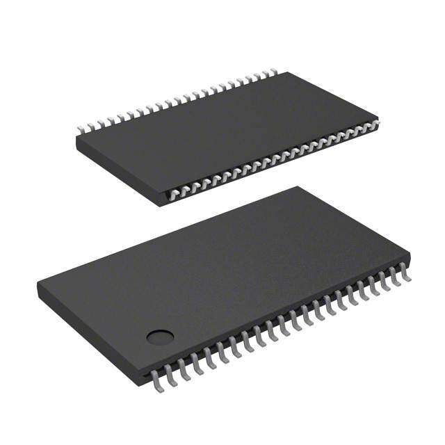
W25Q80BW 3. PACKAGE TYPES W25Q80BW is offered in an 8-pin plastic 150-mil or 208-mil width SOIC (package code SN & SS), an 8- pin VSOP 150-mil or 208-mil (package code SV & ST), 6x5-mm WSON (package code ZP) ), an an 8-pad USON 2x3-mm or 4x-3mm (package code UX & UU) and an 8-ball WLCSP(package code BY) as shown in figure 1a-1c respectively. Package diagrams and dimensions are illustrated at the end of this datasheet. 3.1 Pin Configuration SOIC / VSOP 150 / 208-mil Top View /CS 1 8 VCC DO (IO ) 2 7 /HOLD (IO ) 1 3 /WP (IO ) 3 6 CLK 2 GND 4 5 DI (IO ) 0 Figure 1a. W25Q80BW Pin Assignments, 8-pin SOIC / VSOP 150 / 208-mil (Package Code SN, SS, SV, ST) 3.2 PAD Configuration WSON 6x5-mm, USON 2x3-mm / 4x3-mm Top View /CS 1 8 VCC DO (IO ) 2 7 /HOLD (IO ) 1 3 /WP (IO ) 3 6 CLK 2 GND 4 5 DI (IO ) 0 Figure 1b. W25Q80BW Pad Assignments, 8-pad WSON 6x5-mm, USON 4x3-mm (Package Code ZP & UU) 3.3 Pin Description SOIC / VSOP 150/208-mil, USON 2x3 /4x3-mm, WSON 6x5-mm PIN NO. PIN NAME I/O FUNCTION 1 /CS I Chip Select Input 2 DO (IO1) I/O Data Output (Data Input Output 1)*1 3 /WP (IO2) I/O Write Protect Input ( Data Input Output 2)*2 4 GND Ground 5 DI (IO0) I/O Data Input (Data Input Output 0)*1 6 CLK I Serial Clock Input 7 /HOLD (IO3) I/O Hold Input (Data Input Output 3)*2 8 VCC Power Supply *1 IO0 and IO1 are used for Standard and Dual SPI instructions *2 IO0 – IO3 are used for Quad SPI instructions - 6 -
W25Q80BW 3.4 Ball Configuration WLCSP(WLBGA) Top View Bottom View A1 A2 A2 A1 VCC /CS /CS VCC B1 B2 B2 B1 /HOLD(IO3) DO(IO1) DO(IO1) /HOLD(IO3) C1 C2 C2 C1 CLK /WP(IO2) /WP(IO2) CLK D1 D2 D2 D1 DI(IO0) GND GND DI(IO0) Figure 1c. W25Q80BW Ball Assignments, 8-ball WLCSP (Package Code BY) 3.5 Ball Description WLCSP(WLBGA) BALL NO. PIN NAME I/O FUNCTION A1 VCC Power Supply A2 /CS I Chip Select Input B1 /HOLD (IO3) I/O Hold Input (Data Input Output 3)*2 B2 DO (IO1) I/O Data Output (Data Input Output 1)*1 C1 CLK I Serial Clock Input C2 /WP (IO2) I/O Write Protect Input (Data Input Output 2)*2 D1 DI (IO0) I/O Data Input (Data Input Output 0)*1 D2 GND Ground *1 IO0 and IO1 are used for Standard and Dual SPI instructions *2 IO0 – IO3 are used for Quad SPI instructions Publication Release Date: September 01, 2014 - 7 - Revision L
W25Q80BW 4. PIN DESCRIPTIONS 4.1 Chip Select (/CS) The SPI Chip Select (/CS) pin enables and disables device operation. When /CS is high the device is deselected and the Serial Data Output (DO, or IO0, IO1, IO2, IO3) pins are at high impedance. When deselected, the devices power consumption will be at standby levels unless an internal erase, program or write status register cycle is in progress. When /CS is brought low the device will be selected, power consumption will increase to active levels and instructions can be written to and data read from the device. After power-up, /CS must transition from high to low before a new instruction will be accepted. The /CS input must track the VCC supply level at power-up (see “Write Protection” and figure 37). If needed a pull- up resister on /CS can be used to accomplish this. 4.2 Serial Data Input, Output and IOs (DI, DO and IO0, IO1, IO2, IO3) The W25Q80BW supports standard SPI, Dual SPI and Quad SPI operation. Standard SPI instructions use the unidirectional DI (input) pin to serially write instructions, addresses or data to the device on the rising edge of the Serial Clock (CLK) input pin. Standard SPI also uses the unidirectional DO (output) to read data or status from the device on the falling edge of CLK. Dual and Quad SPI instructions use the bidirectional IO pins to serially write instructions, addresses or data to the device on the rising edge of CLK and read data or status from the device on the falling edge of CLK. Quad SPI instructions require the non-volatile Quad Enable bit (QE) in Status Register-2 to be set. When QE=1, the /WP pin becomes IO2 and /HOLD pin becomes IO3. 4.3 Write Protect (/WP) The Write Protect (/WP) pin can be used to prevent the Status Register from being written. Used in conjunction with the Status Register’s Block Protect (CMP, SEC, TB, BP2, BP1 and BP0) bits and Status Register Protect (SRP) bits, a portion as small as a 4KB sector or the entire memory array can be hardware protected. The /WP pin is active low. When the QE bit of Status Register-2 is set for Quad I/O, the /WP pin function is not available since this pin is used for IO2. See figure 1a-c for the pin configuration of Quad I/O operation. 4.4 HOLD (/HOLD) The /HOLD pin allows the device to be paused while it is actively selected. When /HOLD is brought low, while /CS is low, the DO pin will be at high impedance and signals on the DI and CLK pins will be ignored (don’t care). When /HOLD is brought high, device operation can resume. The /HOLD function can be useful when multiple devices are sharing the same SPI signals. The /HOLD pin is active low. When the QE bit of Status Register-2 is set for Quad I/O, the /HOLD pin function is not available since this pin is used for IO3. See figure 1a-b for the pin configuration of Quad I/O operation. 4.5 Serial Clock (CLK) The SPI Serial Clock Input (CLK) pin provides the timing for serial input and output operations. ("See SPI Operations") - 8 -
W25Q80BW 5. BLOCK DIAGRAM SSeeccuurriittyy RReeggiisstteerr 33 --00 000033000000hh 00003300FFFFhh 000022000000hh 00002200FFFFhh 000011000000hh 00001100FFFFhh BBlloocckk SSeeggmmeennttaattiioonn 000000000000hh 00000000FFFFhh xxxxFFFF0000hh xxxxFFFFFFFFhh FFFFFF0000hh FFFFFFFFFFhh •• SSeeccttoorr 1155 ((44KKBB)) •• •• BBlloocckk 1155 ((6644KKBB)) •• xxxxFF000000hh xxxxFF00FFFFhh FF00000000hh FF0000FFFFhh xxxxEEFF0000hh xxxxEEFFFFFFhh •• SSeeccttoorr 1144 ((44KKBB)) •• xxxxEE000000hh xxxxEE00FFFFhh xxxxDDFF0000hh xxxxDDFFFFFFhh •• SSeeccttoorr 1133 ((44KKBB)) •• xxxxDD000000hh xxxxDD00FFFFhh •• •• •• •• •• •• ee dd oo cc ee DD xxxx22FF0000hh xxxx22FFFFFFhh w w •• SSeeccttoorr 22 ((44KKBB)) •• oo RR xxxx22000000hh xxxx2200FFFFhh d d xxxx11FF0000hh xxxx11FFFFFFhh anan 88FFFF0000hh 88FFFFFFFFhh xxxxxxxxxxxx000101FF0000••••000000000000hhhhhh SSSS eeee cccc tttt oooo rrrr 0101 (((( 4444 KKKK BBBB )))) xxxxxx xxxxxx 010100 FF0000••••FFFFFFFFFFFFhhhhhh Protect Logic Protect Logic 887700FF00FF••••00000000hhhh BBBB llll oooo cccc kkkk 7878 (((( 6666 4444 KKKK BBBB )))) 77 88 FF 00 FF 00 FFFF••••FFFFhhhh W25Q80BWW25Q80BW e e 7700000000hh 770000FFFFhh WritWrit •• •• WWrriittee CCoonnttrrooll //WWPP ((IIOO)) •• 22 LLooggiicc 44FFFF0000hh 44FFFFFFFFhh •• BBlloocckk 44 ((6644KKBB)) •• 4400000000hh 440000FFFFhh SSttaattuuss 33FFFF0000hh 33FFFFFFFFhh RReeggiisstteerr •• BBlloocckk 33 ((6644KKBB)) •• 3300000000hh 330000FFFFhh •• •• HHiigghh VVoollttaaggee •• GGeenneerraattoorrss 0000FFFF0000hh 0000FFFFFFFFhh //HHOOLLDD ((IIOO)) •• BBlloocckk 00 ((6644KKBB)) •• 33 000000000000hh 00000000FFFFhh PPaaggee AAddddrreessss CCLLKK LLaattcchh // CCoouunntteerr BBeeggiinnnniinngg EEnnddiinngg SSPPII PPaaggee AAddddrreessss PPaaggee AAddddrreessss //CCSS CCoommmmaanndd && CCoonnttrrooll LLooggiicc CCoolluummnn DDeeccooddee AAnndd 225566--BByyttee PPaaggee BBuuffffeerr DDaattaa DDII ((IIOO)) 00 DDOO ((IIOO11)) BByyttee AAddddrreessss LLaattcchh // CCoouunntteerr Figure 2. W25Q80BW Serial Flash Memory Block Diagram Publication Release Date: September 01, 2014 - 9 - Revision L
W25Q80BW 6. FUNCTIONAL DESCRIPTION 6.1 SPI OPERATIONS 6.1.1 Standard SPI Instructions The W25Q80BW is accessed through an SPI compatible bus consisting of four signals: Serial Clock (CLK), Chip Select (/CS), Serial Data Input (DI) and Serial Data Output (DO). Standard SPI instructions use the DI input pin to serially write instructions, addresses or data to the device on the rising edge of CLK. The DO output pin is used to read data or status from the device on the falling edge CLK. SPI bus operation Mode 0 (0,0) and 3 (1,1) are supported. The primary difference between Mode 0 and Mode 3 concerns the normal state of the CLK signal when the SPI bus master is in standby and data is not being transferred to the Serial Flash. For Mode 0, the CLK signal is normally low on the falling and rising edges of /CS. For Mode 3, the CLK signal is normally high on the falling and rising edges of /CS. 6.1.2 Dual SPI Instructions The W25Q80BW supports Dual SPI operation when using the “Fast Read Dual Output (3Bh)” and “Fast Read Dual I/O (BBh)” instructions. These instructions allow data to be transferred to or from the device at two to three times the rate of ordinary Serial Flash devices. The Dual SPI Read instructions are ideal for quickly downloading code to RAM upon power-up (code-shadowing) or for executing non-speed-critical code directly from the SPI bus (XIP). When using Dual SPI instructions, the DI and DO pins become bidirectional I/O pins: IO0 and IO1. 6.1.3 Quad SPI Instructions The W25Q80BW supports Quad SPI operation when using the “Fast Read Quad Output (6Bh)”, “Fast Read Quad I/O (EBh)”, “Word Read Quad I/O (E7h)” and “Octal Word Read Quad I/O (E3h)” instructions. These instructions allow data to be transferred to or from the device six to eight times the rate of ordinary Serial Flash. The Quad Read instructions offer a significant improvement in continuous and random access transfer rates allowing fast code-shadowing to RAM or execution directly from the SPI bus (XIP). When using Quad SPI instructions the DI and DO pins become bidirectional IO0 and IO1, and the /WP and /HOLD pins become IO2 and IO3 respectively. Quad SPI instructions require the non-volatile Quad Enable bit (QE) in Status Register-2 to be set. 6.1.4 Hold Function For Standard SPI and Dual SPI operations, the /HOLD signal allows the W25Q80BW operation to be paused while it is actively selected (when /CS is low). The /HOLD function may be useful in cases where the SPI data and clock signals are shared with other devices. For example, consider if the page buffer was only partially written when a priority interrupt requires use of the SPI bus. In this case the /HOLD function can save the state of the instruction and the data in the buffer so programming can resume where it left off once the bus is available again. The /HOLD function is only available for standard SPI and Dual SPI operation, not during Quad SPI. To initiate a /HOLD condition, the device must be selected with /CS low. A /HOLD condition will activate on the falling edge of the /HOLD signal if the CLK signal is already low. If the CLK is not already low the /HOLD condition will activate after the next falling edge of CLK. The /HOLD condition will terminate on the rising edge of the /HOLD signal if the CLK signal is already low. If the CLK is not already low the /HOLD condition will terminate after the next falling edge of CLK. During a /HOLD condition, the Serial Data - 10 -
W25Q80BW Output (DO) is high impedance, and Serial Data Input (DI) and Serial Clock (CLK) are ignored. The Chip Select (/CS) signal should be kept active low for the full duration of the /HOLD operation to avoid resetting the internal logic state of the device. 6.2 WRITE PROTECTION Applications that use non-volatile memory must take into consideration the possibility of noise and other adverse system conditions that may compromise data integrity. To address this concern, the W25Q80BW provides several means to protect the data from inadvertent writes. 6.2.1 Write Protect Features Device resets when VCC is below threshold Time delay write disable after Power-up Write enable/disable instructions and automatic write disable after erase or program Software and Hardware (/WP pin) write protection using Status Register Write Protection using Power-down instruction Lock Down write protection until next power-up One Time Program (OTP) write protection* * Note: This feature is available upon special order. Please contact Winbond for details. Upon power-up or at power-down, the W25Q80BW will maintain a reset condition while VCC is below the threshold value of VWI, (See Power-up Timing and Voltage Levels and Figure 37). While reset, all operations are disabled and no instructions are recognized. During power-up and after the VCC voltage exceeds VWI, all program and erase related instructions are further disabled for a time delay of tPUW. This includes the Write Enable, Page Program, Sector Erase, Block Erase, Chip Erase and the Write Status Register instructions. Note that the chip select pin (/CS) must track the VCC supply level at power-up until the VCC-min level and tVSL time delay is reached. If needed a pull-up resister on /CS can be used to accomplish this. After power-up the device is automatically placed in a write-disabled state with the Status Register Write Enable Latch (WEL) set to a 0. A Write Enable instruction must be issued before a Page Program, Sector Erase, Block Erase, Chip Erase or Write Status Register instruction will be accepted. After completing a program, erase or write instruction the Write Enable Latch (WEL) is automatically cleared to a write- disabled state of 0. Software controlled write protection is facilitated using the Write Status Register instruction and setting the Status Register Protect (SRP0, SRP1) and Block Protect (CMP, SEC,TB, BP2, BP1 and BP0) bits. These settings allow a portion as small as 4KB sector or the entire memory array to be configured as read only. Used in conjunction with the Write Protect (/WP) pin, changes to the Status Register can be enabled or disabled under hardware control. See Status Register section for further information. Additionally, the Power-down instruction offers an extra level of write protection as all instructions are ignored except for the Release Power-down instruction. Publication Release Date: September 01, 2014 - 11 - Revision L
W25Q80BW 7. STATUS REGISTERS AND INSTRUCTIONS The Read Status Register-1 and Status Register-2 instructions can be used to provide status on the availability of the Flash memory array, if the device is write enabled or disabled, the state of write protection, Quad SPI setting, Security Register lock status and Erase/Program Suspend status. The Write Status Register instruction can be used to configure the device write protection features, Quad SPI setting and Security Register OTP lock. Write access to the Status Register is controlled by the state of the non- volatile Status Register Protect bits (SRP0, SRP1), the Write Enable instruction, and during Standard/Dual SPI operations, the /WP pin. 7.1 STATUS REGISTERs 7.1.1 BUSY Status (BUSY) BUSY is a read only bit in the status register (S0) that is set to a 1 state when the device is executing a Page Program, Quad Page Program, Sector Erase, Block Erase, Chip Erase, Write Status Register or Erase/Program Security Register instruction. During this time the device will ignore further instructions except for the Read Status Register and Erase/Program Suspend instruction (see tW, tPP, tSE, tBE, and tCE in AC Characteristics). When the program, erase or write status/security register instruction has completed, the BUSY bit will be cleared to a 0 state indicating the device is ready for further instructions. 7.1.2 Write Enable Latch Status (WEL) Write Enable Latch (WEL) is a read only bit in the status register (S1) that is set to 1 after executing a Write Enable Instruction. The WEL status bit is cleared to 0 when the device is write disabled. A write disable state occurs upon power-up or after any of the following instructions: Write Disable, Page Program, Quad Page Program, Sector Erase, Block Erase, Chip Erase, Write Status Register, Erase Security Register and Program Security Register. 7.1.3 Block Protect Bits (BP2, BP1, BP0) The Block Protect Bits (BP2, BP1, BP0) are non-volatile read/write bits in the status register (S4, S3, and S2) that provide Write Protection control and status. Block Protect bits can be set using the Write Status Register Instruction (see tW in AC characteristics). All, none or a portion of the memory array can be protected from Program and Erase instructions (see Status Register Memory Protection table). The factory default setting for the Block Protection Bits is 0, none of the array protected. 7.1.4 Top/Bottom Block Protect (TB) The non-volatile Top/Bottom bit (TB) controls if the Block Protect Bits (BP2, BP1, BP0) protect from the Top (TB=0) or the Bottom (TB=1) of the array as shown in the Status Register Memory Protection table. The factory default setting is TB=0. The TB bit can be set with the Write Status Register Instruction depending on the state of the SRP0, SRP1 and WEL bits. 7.1.5 Sector/Block Protect (SEC) The non-volatile Sector/Block Protect bit (SEC) controls if the Block Protect Bits (BP2, BP1, BP0) protect either 4KB Sectors (SEC=1) or 64KB Blocks (SEC=0) in the Top (TB=0) or the Bottom (TB=1) of the array as shown in the Status Register Memory Protection table. The default setting is SEC=0. - 12 -
W25Q80BW 7.1.6 Complement Protect (CMP) The Complement Protect bit (CMP) is a non-volatile read/write bit in the status register (S14). It is used in conjunction with SEC, TB, BP2, BP1 and BP0 bits to provide more flexibility for the array protection. Once CMP is set to 1, previous array protection set by SEC, TB, BP2, BP1 and BP0 will be reversed. For instance, when CMP=0, a top 4KB sector can be protected while the rest of the array is not; when CMP=1, the top 4KB sector will become unprotected while the rest of the array become read-only. Please refer to the Status Register Memory Protection table for details. The default setting is CMP=0. 7.1.7 Status Register Protect (SRP1, SRP0) The Status Register Protect bits (SRP1 and SRP0) are non-volatile read/write bits in the status register (S8 and S7). The SRP bits control the method of write protection: software protection, hardware protection, power supply lock-down or one time programmable (OTP) protection. Status SRP1 SRP0 /WP Description Register Software /WP pin has no control. The Status register can be written to 0 0 X Protection after a Write Enable instruction, WEL=1. [Factory Default] Hardware When /WP pin is low the Status Register locked and can not 0 1 0 Protected be written to. Hardware When /WP pin is high the Status register is unlocked and can 0 1 1 Unprotected be written to after a Write Enable instruction, WEL=1. Power Supply Status Register is protected and can not be written to again 1 0 X Lock-Down until the next power-down, power-up cycle.(1) One Time Status Register is permanently protected and can not be 1 1 X Program(2) written to. Notes: 1. When SRP1, SRP0 = (1, 0), a power-down, power-up cycle will change SRP1, SRP0 to (0, 0) state. 2. This feature is available upon special order. Please contact Winbond for details. 7.1.8 Erase/Program Suspend Status (SUS) The Suspend Status bit is a read only bit in the status register (S15) that is set to 1 after executing a Erase/Program Suspend (75h) instruction. The SUS status bit is cleared to 0 by Erase/Program Resume (7Ah) instruction as well as a power-down, power-up cycle. 7.1.9 Security Register Lock Bits (LB3, LB2, LB1, LB0) The Security Register Lock Bits (LB3, LB2, LB1, LB0) are non-volatile One Time Program (OTP) bits in Status Register (S13, S12, S11,S10) that provide the write protect control and status to the Security Registers. The default state of LB3-0 is 0, Security Registers are unlocked. LB3-0 can be set to 1 individually using the Write Status Register instruction. LB3-0 are One Time Programmable (OTP), once it’s set to 1, the corresponding 256-Byte Security Register will become read-only permanently. Publication Release Date: September 01, 2014 - 13 - Revision L
W25Q80BW 7.1.10 Quad Enable (QE) The Quad Enable (QE) bit is a non-volatile read/write bit in the status register (S9) that allows Quad SPI operation. When the QE bit is set to a 0 state (factory default), the /WP pin and /HOLD are enabled. When the QE bit is set to a 1, the Quad IO2 and IO3 pins are enabled, and /WP and /HOLD functions are disabled. WARNING: If the /WP or /HOLD pins are tied directly to the power supply or ground during standard SPI or Dual SPI operation, the QE bit should never be set to a 1. SS77 SS66 SS55 SS44 SS33 SS22 SS11 SS00 SSRRPP00 SSEECC TTBB BBPP22 BBPP11 BBPP00 WWEELL BBUUSSYY SSTTAATTUUSS RREEGGIISSTTEERR PPRROOTTEECCTT 00 ((nnoonn--vvoollaattiillee)) SSEECCTTOORR PPRROOTTEECCTT ((nnoonn--vvoollaattiillee)) TTOOPP//BBOOTTTTOOMM PPRROOTTEECCTT ((nnoonn--vvoollaattiillee)) BBLLOOCCKK PPRROOTTEECCTT BBIITTSS ((nnoonn--vvoollaattiillee)) WWRRIITTEE EENNAABBLLEE LLAATTCCHH EERRAASSEE//WWRRIITTEE IINN PPRROOGGRREESSSS Figure 3a. Status Register-1 SS1155 SS1144 SS1133 SS1122 SS1111 SS1100 SS99 SS88 SSUUSS CCMMPP LLBB33 LLBB22 LLBB11 L B0 QQEE SSRRPP11 SSUUSSPPEENNDD SSTTAATTUUSS CCOOMMPPLLEEMMEENNTT PPRROOTTEECCTT ((nnoonn - - v voollaattiillee)) SSEECCUURRIITTYY RREEGGIISSTTEERR LLOOCCKK BBIITTSS ((nnoonn -- v voollaattiillee OOTTPP)) QQUUAADD EENNAABBLLEE ((nnoonn - - v voollaattiillee)) SSTTAATTUUSS RREEGGIISSTTEERR PPRROOTTEECCTT 11 ((nnoonn - - v voollaattiillee)) Figure 3b. Status Register-2 - 14 -
W25Q80BW 7.1.11 Status Register Memory Protection (CMP = 0) STATUS REGISTER(1) W25Q80BW (8M-BIT) MEMORY PROTECTION(2) SEC TB BP2 BP1 BP0 BLOCK(S) ADDRESSES DENSITY PORTION X X 0 0 0 NONE NONE NONE NONE 0 0 0 0 1 15 0F0000h – 0FFFFFh 64KB Upper 1/16 0 0 0 1 0 14 and 15 0E0000h – 0FFFFFh 128KB Upper 1/8 0 0 0 1 1 12 thru 15 0C0000h – 0FFFFFh 256KB Upper 1/4 0 0 1 0 0 8 thru 15 080000h – 0FFFFFh 512KB Upper 1/2 0 1 0 0 1 0 000000h – 00FFFFh 64KB Lower 1/16 0 1 0 1 0 0 and 1 000000h – 01FFFFh 128KB Lower 1/8 0 1 0 1 1 0 thru 3 000000h – 03FFFFh 256KB Lower 1/4 0 1 1 0 0 0 thru 7 000000h – 07FFFFh 512KB Lower 1/2 0 X 1 0 1 0 thru 15 000000h – 0FFFFFh 1MB ALL 0 X 1 1 X 0 thru 15 000000h – 0FFFFFh 1MB ALL 1 0 0 0 1 15 0FF000h – 0FFFFFh 4KB Upper 1/256 1 0 0 1 0 15 0FE000h – 0FFFFFh 8KB Upper 1/128 1 0 0 1 1 15 0FC000h – 0FFFFFh 16KB Upper 1/64 1 0 1 0 X 15 0F8000h – 0FFFFFh 32KB Upper 1/32 1 1 0 0 1 0 000000h – 000FFFh 4KB Lower 1/256 1 1 0 1 0 0 000000h – 001FFFh 8KB Lower 1/128 1 1 0 1 1 0 000000h – 003FFFh 16KB Lower 1/64 1 1 1 0 X 0 000000h – 007FFFh 32KB Lower 1/32 1 X 1 1 1 0 thru 15 000000h – 0FFFFFh 1MB ALL Notes: 1. X = don’t care 2. If any Erase or Program command specifies a memory region that contains protected data portion, this command will be ignored. Publication Release Date: September 01, 2014 - 15 - Revision L
W25Q80BW 7.1.12 Status Register Memory Protection (CMP = 1) STATUS REGISTER(1) W25Q80BW (8M-BIT) MEMORY PROTECTION(2) SEC TB BP2 BP1 BP0 BLOCK(S) ADDRESSES DENSITY PORTION X X 0 0 0 0 thru 15 000000h – 0FFFFFh 1MB ALL 0 0 0 0 1 0 thru 14 000000h – 0EFFFFh 960KB Lower 15/16 0 0 0 1 0 0 thru 13 000000h – 0DFFFFh 896KB Lower 7/8 0 0 0 1 1 0 thru 11 000000h – 0BFFFFh 768KB Lower 3/4 0 0 1 0 0 0 thru 7 000000h – 07FFFFh 512KB Lower 1/2 0 1 0 0 1 1 thru 15 010000h – 0FFFFFh 960KB Upper 15/16 0 1 0 1 0 2 thru 15 020000h – 0FFFFFh 896KB Upper 7/8 0 1 0 1 1 4 thru 15 040000h – 0FFFFFh 768KB Upper 3/4 0 1 1 0 0 8 thru 15 080000h – 0FFFFFh 512KB Upper 1/2 0 X 1 0 1 NONE NONE NONE NONE 0 X 1 1 X NONE NONE NONE NONE 1 0 0 0 1 0 thru 15 000000h – 0FEFFFh 1,020KB Lower 255/256 1 0 0 1 0 0 thru 15 000000h – 0FDFFFh 1,016KB Lower 127/128 1 0 0 1 1 0 thru 15 000000h – 0FBFFFh 1,008KB Lower 63/64 1 0 1 0 X 0 thru 15 000000h – 0F7FFFh 992KB Lower 31/32 1 1 0 0 1 0 thru 15 001000h – 0FFFFFh 1,020KB Upper 255/256 1 1 0 1 0 0 thru 15 002000h – 0FFFFFh 1,016KB Upper 127/128 1 1 0 1 1 0 thru 15 004000h – 0FFFFFh 1,008KB Upper 63/64 1 1 1 0 X 0 thru 15 008000h – 0FFFFFh 992KB Upper 31/32 1 X 1 1 1 NONE NONE NONE NONE Notes: 1. X = don’t care 2. If any Erase or Program command specifies a memory region that contains protected data portion, this command will be ignored. - 16 -
W25Q80BW 7.2 INSTRUCTIONS The instruction set of the W25Q80BW consists of thirty four basic instructions that are fully controlled through the SPI bus (see Instruction Set table1-3). Instructions are initiated with the falling edge of Chip Select (/CS). The first byte of data clocked into the DI input provides the instruction code. Data on the DI input is sampled on the rising edge of clock with most significant bit (MSB) first. Instructions vary in length from a single byte to several bytes and may be followed by address bytes, data bytes, dummy bytes (don’t care), and in some cases, a combination. Instructions are completed with the rising edge of edge /CS. Clock relative timing diagrams for each instruction are included in figures 4 through 36. All read instructions can be completed after any clocked bit. However, all instructions that Write, Program or Erase must complete on a byte boundary (/CS driven high after a full 8-bits have been clocked) otherwise the instruction will be ignored. This feature further protects the device from inadvertent writes. Additionally, while the memory is being programmed or erased, or when the Status Register is being written, all instructions except for Read Status Register will be ignored until the program or erase cycle has completed. 7.2.1 Manufacturer and Device Identification MANUFACTURER ID (MF7-MF0) Winbond Serial Flash EFh Device ID (ID7-ID0) (ID15-ID0) Instruction ABh, 90h, 92h, 94h 9Fh W25Q80BW 13h 5014h Publication Release Date: September 01, 2014 - 17 - Revision L
W25Q80BW 7.2.2 Instruction Set Table 1 (Erase, Program Instructions)(1) BYTE 1 INSTRUCTION NAME BYTE 2 BYTE 3 BYTE 4 BYTE 5 BYTE 6 (CODE) Write Enable 06h Write Enable for 50h Volatile Status Register Write Disable 04h Read Status Register-1 05h (S7–S0) (2) Read Status Register-2 35h (S15–S8) (2) Write Status Register 01h S7–S0 S15-S8 Page Program 02h A23–A16 A15–A8 A7–A0 D7–D0 Quad Page Program 32h A23–A16 A15–A8 A7–A0 D7–D0, …(3) Sector Erase (4KB) 20h A23–A16 A15–A8 A7–A0 Block Erase (32KB) 52h A23–A16 A15–A8 A7–A0 Block Erase (64KB) D8h A23–A16 A15–A8 A7–A0 Chip Erase C7h/60h Erase / Program 75h Suspend(5) Erase / Program 7Ah Resume(5) Power-down B9h Continuous Read Mode FFh FFh Reset (4) Notes: 1. Data bytes are shifted with Most Significant Bit first. Byte fields with data in parenthesis “()” indicate data being read from the device on the DO pin. 2. The Status Register contents will repeat continuously until /CS terminates the instruction. 3. Quad Page Program Input Data: IO0 = D4, D0, …… IO1 = D5, D1, …… IO2 = D6, D2, …… IO3 = D7, D3, …… 4. This instruction is recommended when using the Dual or Quad “Continuous Read Mode” feature. See section 7.2.19 & 7.2.20 for more information. 5. For Suspend/Resume feature, please contact Winbond for detailed information. - 18 -
W25Q80BW 7.2.3 Instruction Set Table 2 (Read Instructions) BYTE 1 INSTRUCTION NAME BYTE 2 BYTE 3 BYTE 4 BYTE 5 BYTE 6 (CODE) Read Data 03h A23-A16 A15-A8 A7-A0 (D7-D0) Fast Read 0Bh A23-A16 A15-A8 A7-A0 dummy (D7-D0) Fast Read Dual Output 3Bh A23-A16 A15-A8 A7-A0 dummy (D7-D0, …)(1) Fast Read Quad Output 6Bh A23-A16 A15-A8 A7-A0 dummy (D7-D0, …)(3) Fast Read Dual I/O BBh A23-A8(2) A7-A0, M7-M0(2) (D7-D0, …)(1) (x,x,x,x, D7-D0, Fast Read Quad I/O EBh A23-A0, M7-M0(4) (D7-D0, …)(3) …)(5) Word Read Quad I/O(7) E7h A23-A0, M7-M0(4) (x,x, D7-D0, …)(6) (D7-D0, …)(3) Octal Word Read Quad I/O(8) E3h A23-A0, M7-M0(4) (D7-D0, …)(3) Set Burst with Wrap 77h xxxxxx, W6-W4(4) Notes: 1. Dual Output data IO0 = (D6, D4, D2, D0) IO1 = (D7, D5, D3, D1) 2. Dual Input Address IO0 = A22, A20, A18, A16, A14, A12, A10, A8 A6, A4, A2, A0, M6, M4, M2, M0 IO1 = A23, A21, A19, A17, A15, A13, A11, A9 A7, A5, A3, A1, M7, M5, M3, M1 3. Quad Output Data IO0 = (D4, D0, …..) IO1 = (D5, D1, …..) IO2 = (D6, D2, …..) IO3 = (D7, D3, …..) 4. Quad Input Address Set Burst with Wrap Input IO0 = A20, A16, A12, A8, A4, A0, M4, M0 IO0 = x, x, x, x, x, x, W4, x IO1 = A21, A17, A13, A9, A5, A1, M5, M1 IO1 = x, x, x, x, x, x, W5, x IO2 = A22, A18, A14, A10, A6, A2, M6, M2 IO2 = x, x, x, x, x, x, W6, x IO3 = A23, A19, A15, A11, A7, A3, M7, M3 IO3 = x, x, x, x, x, x, x, x 5. Fast Read Quad I/O Data IO0 = (x, x, x, x, D4, D0, …..) IO1 = (x, x, x, x, D5, D1, …..) IO2 = (x, x, x, x, D6, D2, …..) IO3 = (x, x, x, x, D7, D3, …..) 6. Word Read Quad I/O Data IO0 = (x, x, D4, D0, …..) IO1 = (x, x, D5, D1, …..) IO2 = (x, x, D6, D2, …..) IO3 = (x, x, D7, D3, …..) 7. The lowest address bit must be 0. ( A0 = 0 ) 8. The lowest 4 address bits must be 0. ( A0, A1, A2, A3 = 0 ) Publication Release Date: September 01, 2014 - 19 - Revision L
W25Q80BW 7.2.4 Instruction Set Table 3 (ID, Security Instructions) INSTRUCTION BYTE 1 BYTE 2 BYTE 3 BYTE 4 BYTE 5 BYTE 6 NAME (CODE) Release Power down/ ABh dummy dummy dummy (ID7-ID0)(1) Device ID Manufacturer/ 90h dummy dummy 00h (MF7-MF0) (ID7-ID0) Device ID(2) Manufacturer/Device ID 92h A23-A8 A7-A0, M[7:0] (MF[7:0], ID[7:0]) by Dual I/O Manufacture/Device ID 94h A23-A0, M[7:0] xxxx, (MF[7:0], ID[7:0]) (MF[7:0], ID[7:0], …) by Quad I/O (MF7-MF0) (ID15-ID8) (ID7-ID0) JEDEC ID 9Fh Manufacturer Memory Type Capacity Read Unique ID 4Bh dummy dummy dummy dummy (ID63-ID0) Erase 44h A23–A16 A15–A8 A7–A0 Security Registers(3) Program 42h A23–A16 A15–A8 A7–A0 D7-D0 D7-D0 Security Registers(3) Read 48h A23–A16 A15–A8 A7–A0 dummy (D7-0) Security Registers(3) Notes: 1. The Device ID will repeat continuously until /CS terminates the instruction. 2. See Manufacturer and Device Identification table for Device ID information. 3. Security Register Address: Security Register 0: A23-16 = 00h; A15-8 = 00h; A7-0 = byte address Security Register 1: A23-16 = 00h; A15-8 = 10h; A7-0 = byte address Security Register 2: A23-16 = 00h; A15-8 = 20h; A7-0 = byte address Security Register 3: A23-16 = 00h; A15-8 = 30h; A7-0 = byte address Please note that Security Register 0 is Reserved by Winbond for future use. It is recommended to use Security registers 1- 3 before using register 0 - 20 -
W25Q80BW 7.2.5 Write Enable (06h) The Write Enable instruction (Figure 4) sets the Write Enable Latch (WEL) bit in the Status Register to a 1. The WEL bit must be set prior to every Page Program, Quad Page Program, Sector Erase, Block Erase, Chip Erase, Write Status Register and Erase/Program Security Registers instruction. The Write Enable instruction is entered by driving /CS low, shifting the instruction code “06h” into the Data Input (DI) pin on the rising edge of CLK, and then driving /CS high. /CS Mode 3 0 1 2 3 4 5 6 7 Mode 3 CLK Mode 0 Mode 0 Instruction (06h) DI (IO ) 0 DO High Impedance (IO ) 1 Figure 4. Write Enable Instruction Sequence Diagram 7.2.6 Write Enable for Volatile Status Register (50h) The non-volatile Status Register bits described in section 8.1 can also be written to as volatile bits. This gives more flexibility to change the system configuration and memory protection schemes quickly without waiting for the typical non-volatile bit write cycles or affecting the endurance of the Status Register non- volatile bits. To write the volatile values into the Status Register bits, the Write Enable for Volatile Status Register (50h) instruction must be issued prior to a Write Status Register (01h) instruction. Write Enable for Volatile Status Register instruction (Figure 5) will not set the Write Enable Latch (WEL) bit, it is only valid for the Write Status Register instruction to change the volatile Status Register bit values. /CS Mode 3 0 1 2 3 4 5 6 7 Mode 3 CLK Mode 0 Mode 0 Instruction (50h) DI (IO ) 0 DO High Impedance (IO ) 1 Figure 5. Write Enable for Volatile Status Register Instruction Sequence Diagram Publication Release Date: September 01, 2014 - 21 - Revision L
W25Q80BW 7.2.7 Write Disable (04h) The Write Disable instruction (Figure 6) resets the Write Enable Latch (WEL) bit in the Status Register to a 0. The Write Disable instruction is entered by driving /CS low, shifting the instruction code “04h” into the DI pin and then driving /CS high. Note that the WEL bit is automatically reset after Power-up and upon completion of the Write Status Register, Erase/Program Security Registers, Page Program, Quad Page Program, Sector Erase, Block Erase and Chip Erase instructions. Write Disable instruction can also be used to invalidate the Write Enable for Volatile Status Register instruction. /CS Mode 3 0 1 2 3 4 5 6 7 Mode 3 CLK Mode 0 Mode 0 Instruction (04h) DI (IO ) 0 DO High Impedance (IO ) 1 Figure 6. Write Disable Instruction Sequence Diagram - 22 -
W25Q80BW 7.2.8 Read Status Register-1 (05h) and Read Status Register-2 (35h) The Read Status Register instructions allow the 8-bit Status Registers to be read. The instruction is entered by driving /CS low and shifting the instruction code “05h” for Status Register-1 or “35h” for Status Register-2 into the DI pin on the rising edge of CLK. The status register bits are then shifted out on the DO pin at the falling edge of CLK with most significant bit (MSB) first as shown in figure 7. The Status Register bits are shown in figure 3a and 3b and include the BUSY, WEL, BP2-BP0, TB, SEC, SRP0, SRP1, QE, LB3-0, CMP and SUS bits (see Status Register section earlier in this datasheet). The Read Status Register instruction may be used at any time, even while a Program, Erase or Write Status Register cycle is in progress. This allows the BUSY status bit to be checked to determine when the cycle is complete and if the device can accept another instruction. The Status Register can be read continuously, as shown in Figure 7. The instruction is completed by driving /CS high. /CS Mode 3 0 1 2 3 4 5 6 7 8 9 10 11 12 13 14 15 16 17 18 19 20 21 22 23 CLK Mode 0 Instruction (05h or 35h) DI (IO) 0 Status Register 1 or 2 out Status Register 1 or 2 out DO High Impedance 7 6 5 4 3 2 1 0 7 6 5 4 3 2 1 0 7 (IO) 1 *= MSB * * Figure 7. Read Status Register Instruction Sequence Diagram 7.2.9 Write Status Register (01h) The Write Status Register instruction allows the Status Register to be written. Only non-volatile Status Register bits SRP0, SEC, TB, BP2, BP1, BP0 (bits 7 thru 2 of Status Register-1) and CMP, LB3, LB2, LB1,LB0, QE, SRP1 (bits 14 thru 8 of Status Register-2) can be written to. All other Status Register bit locations are read-only and will not be affected by the Write Status Register instruction. LB3-0 are non- volatile OTP bits, once it is set to 1, it can not be cleared to 0. The Status Register bits are shown in figure 3a and 3b and described in 8.1. To write non-volatile Status Register bits, a standard Write Enable (06h) instruction must previously have been executed for the device to accept the Write Status Register Instruction (Status Register bit WEL must equal 1). Once write enabled, the instruction is entered by driving /CS low, sending the instruction code “01h”, and then writing the status register data byte as illustrated in figure 8. To write volatile Status Register bits, a Write Enable for Volatile Status Register (50h) instruction must have been executed prior to the Write Status Register instruction (Status Register bit WEL remains 0). However, SRP1 and LB3, LB2, LB1, LB0 can not be changed from “1” to “0” because of the OTP protection for these bits. Upon power off, the volatile Status Register bit values will be lost, and the non- volatile Status Register bit values will be restored when power on again. Publication Release Date: September 01, 2014 - 23 - Revision L
W25Q80BW To complete the Write Status Register instruction, the /CS pin must be driven high after the eighth or sixteenth bit of data that is clocked in. If this is not done the Write Status Register instruction will not be executed. If /CS is driven high after the eighth clock (compatible with the 25X series) the CMP, QE and SRP1 bits will be cleared to 0. During non-volatile Status Register write operation (06h combined with 01h), after /CS is driven high, the self-timed Write Status Register cycle will commence for a time duration of tW (See AC Characteristics). While the Write Status Register cycle is in progress, the Read Status Register instruction may still be accessed to check the status of the BUSY bit. The BUSY bit is a 1 during the Write Status Register cycle and a 0 when the cycle is finished and ready to accept other instructions again. After the Write Status Register cycle has finished, the Write Enable Latch (WEL) bit in the Status Register will be cleared to 0. During volatile Status Register write operation (50h combined with 01h), after /CS is driven high, the Status Register bits will be refreshed to the new values within the time period of tSHSL2 (See AC Characteristics). BUSY bit will remain 0 during the Status Register bit refresh period. Please refer to 8.1 for detailed Status Register Bit descriptions. Factory default for all status Register bits are 0. /CS Mode 3 0 1 2 3 4 5 6 7 8 9 10 11 12 13 14 15 16 17 18 19 20 21 22 23 Mode 3 CLK Mode 0 Mode 0 Instruction (01h) Status Register 1 in Status Register 2 in DI 7 6 5 4 3 2 1 0 15 14 13 12 11 10 9 8 (IO) 0 * * DO High Impedance (IO) 1 *= MSB Figure 8. Write Status Register Instruction Sequence Diagram - 24 -
W25Q80BW 7.2.10 Read Data (03h) The Read Data instruction allows one or more data bytes to be sequentially read from the memory. The instruction is initiated by driving the /CS pin low and then shifting the instruction code “03h” followed by a 24-bit address (A23-A0) into the DI pin. The code and address bits are latched on the rising edge of the CLK pin. After the address is received, the data byte of the addressed memory location will be shifted out on the DO pin at the falling edge of CLK with most significant bit (MSB) first. The address is automatically incremented to the next higher address after each byte of data is shifted out allowing for a continuous stream of data. This means that the entire memory can be accessed with a single instruction as long as the clock continues. The instruction is completed by driving /CS high. The Read Data instruction sequence is shown in figure 9. If a Read Data instruction is issued while an Erase, Program or Write cycle is in process (BUSY=1) the instruction is ignored and will not have any effects on the current cycle. The Read Data instruction allows clock rates from D.C. to a maximum of fR (see AC Electrical Characteristics). /CS Mode 3 0 1 2 3 4 5 6 7 8 9 10 28 29 30 31 32 33 34 35 36 37 38 39 CLK Mode 0 Instruction (03h) 24-Bit Address DI 23 22 21 3 2 1 0 (IO) 0 * Data Out 1 DO High Impedance 7 6 5 4 3 2 1 0 7 (IO) 1 * *= MSB Figure 9. Read Data Instruction Sequence Diagram Publication Release Date: September 01, 2014 - 25 - Revision L
W25Q80BW 7.2.11 Fast Read (0Bh) The Fast Read instruction is similar to the Read Data instruction except that it can operate at the highest possible frequency of FR (see AC Electrical Characteristics). This is accomplished by adding eight “dummy” clocks after the 24-bit address as shown in figure 10. The dummy clocks allow the devices internal circuits additional time for setting up the initial address. During the dummy clocks the data value on the DO pin is a “don’t care”. /CS Mode 3 0 1 2 3 4 5 6 7 8 9 10 28 29 30 31 CLK Mode 0 Instruction (0Bh) 24-Bit Address DI 23 22 21 3 2 1 0 (IO) 0 * DO High Impedance (IO) 1 *= MSB /CS 31 32 33 34 35 36 37 38 39 40 41 42 43 44 45 46 47 48 49 50 51 52 53 54 55 CLK Dummy Clocks DI 0 (IO) 0 Data Out 1 Data Out 2 DO High Impedance 7 6 5 4 3 2 1 0 7 6 5 4 3 2 1 0 7 (IO) 1 * * Figure 10. Fast Read Instruction Sequence Diagram - 26 -
W25Q80BW 7.2.12 Fast Read Dual Output (3Bh) The Fast Read Dual Output (3Bh) instruction is similar to the standard Fast Read (0Bh) instruction except that data is output on two pins; IO and IO . This allows data to be transferred from the W25Q80BW at 0 1 twice the rate of standard SPI devices. The Fast Read Dual Output instruction is ideal for quickly downloading code from Flash to RAM upon power-up or for applications that cache code-segments to RAM for execution. Similar to the Fast Read instruction, the Fast Read Dual Output instruction can operate at the highest possible frequency of FR (see AC Electrical Characteristics). This is accomplished by adding eight “dummy” clocks after the 24-bit address as shown in figure 11. The dummy clocks allow the device's internal circuits additional time for setting up the initial address. The input data during the dummy clocks is “don’t care”. However, the IO pin should be high-impedance prior to the falling edge of the first data out 0 clock. /CS Mode 3 0 1 2 3 4 5 6 7 8 9 10 28 29 30 31 CLK Mode 0 Instruction (3Bh) 24-Bit Address DI 23 22 21 3 2 1 0 (IO) 0 * DO High Impedance (IO) 1 *= MSB /CS 31 32 33 34 35 36 37 38 39 40 41 42 43 44 45 46 47 48 49 50 51 52 53 54 55 CLK IO switches from Dummy Clocks 0 Input to Output DI 0 6 4 2 0 6 4 2 0 6 4 2 0 6 4 2 0 6 (IO) 0 DO High Impedance 7 5 3 1 7 5 3 1 7 5 3 1 7 5 3 1 7 (IO) 1 * Data Out 1 * Data Out 2 * Data Out 3 * Data Out 4 Figure 11. Fast Read Dual Output Instruction Sequence Diagram Publication Release Date: September 01, 2014 - 27 - Revision L
W25Q80BW 7.2.13 Fast Read Quad Output (6Bh) The Fast Read Quad Output (6Bh) instruction is similar to the Fast Read Dual Output (3Bh) instruction except that data is output on four pins, IO , IO , IO , and IO . A Quad enable of Status Register-2 must be 0 1 2 3 executed before the device will accept the Fast Read Quad Output Instruction (Status Register bit QE must equal 1). The Fast Read Quad Output Instruction allows data to be transferred from the W25Q80BW at four times the rate of standard SPI devices. The Fast Read Quad Output instruction can operate at the highest possible frequency of FR (see AC Electrical Characteristics). This is accomplished by adding eight “dummy” clocks after the 24-bit address as shown in figure 12. The dummy clocks allow the device's internal circuits additional time for setting up the initial address. The input data during the dummy clocks is “don’t care”. However, the IO pins should be high-impedance prior to the falling edge of the first data out clock. /CS Mode 3 0 1 2 3 4 5 6 7 8 9 10 28 29 30 31 CLK Mode 0 Instruction (6Bh) 24-Bit Address IO 23 22 21 3 2 1 0 0 * High Impedance IO 1 High Impedance IO 2 High Impedance IO 3 *= MSB /CS 31 32 33 34 35 36 37 38 39 40 41 42 43 44 45 46 47 CLK IO switches from Dummy Clocks 0 Input to Output IO 0 4 0 4 0 4 0 4 0 4 0 High Impedance IO 5 1 5 1 5 1 5 1 5 1 High Impedance IO 6 2 6 2 6 2 6 2 6 2 High Impedance IO 7 3 7 3 7 3 7 3 7 3 Byte 1 Byte 2 Byte 3 Byte 4 Figure 12. Fast Read Quad Output Instruction Sequence Diagram - 28 -
W25Q80BW 7.2.14 Fast Read Dual I/O (BBh) The Fast Read Dual I/O (BBh) instruction allows for improved random access while maintaining two IO pins, IO and IO . It is similar to the Fast Read Dual Output (3Bh) instruction but with the capability to input 0 1 the Address bits (A23-0) two bits per clock. This reduced instruction overhead may allow for code execution (XIP) directly from the Dual SPI in some applications. Fast Read Dual I/O with “Continuous Read Mode” The Fast Read Dual I/O instruction can further reduce instruction overhead through setting the “Continuous Read Mode” bits (M7-0) after the input Address bits (A23-0), as shown in figure 13a. The upper nibble of the (M7-4) controls the length of the next Fast Read Dual I/O instruction through the inclusion or exclusion of the first byte instruction code. The lower nibble bits of the (M3-0) are don’t care (“x”). However, the IO pins should be high-impedance prior to the falling edge of the first data out clock. If the “Continuous Read Mode” bits M5-4 = (1,0), then the next Fast Read Dual I/O instruction (after /CS is raised and then lowered) does not require the BBh instruction code, as shown in figure 13b. This reduces the instruction sequence by eight clocks and allows the Read address to be immediately entered after /CS is asserted low. If the “Continuous Read Mode” bits M5-4 do not equal to (1,0), the next instruction (after /CS is raised and then lowered) requires the first byte instruction code, thus returning to normal operation. A “Continuous Read Mode” Reset instruction can also be used to reset (M7-0) before issuing normal instructions (See 7.2.20 for detail descriptions). /CS Mode 3 0 1 2 3 4 5 6 7 8 9 10 11 12 13 14 15 16 17 18 19 20 21 22 23 CLK Mode 0 Instruction (BBh) A23-16 A15-8 A7-0 M7-0 DI 22 20 18 16 14 12 10 8 6 4 2 0 6 4 2 0 (IO) 0 DO 23 21 19 17 15 13 11 9 7 5 3 1 7 5 3 1 (IO) 1 * * *= MSB /CS 23 24 25 26 27 28 29 30 31 32 33 34 35 36 37 38 39 CLK IOs switch from Input to Output DI 0 6 4 2 0 6 4 2 0 6 4 2 0 6 4 2 0 6 (IO) 0 DO 1 7 5 3 1 7 5 3 1 7 5 3 1 7 5 3 1 7 (IO) 1 * * * * Byte 1 Byte 2 Byte 3 Byte 4 Figure 13a. Fast Read Dual I/O Instruction Sequence (Initial instruction or previous M5-4 10) Publication Release Date: September 01, 2014 - 29 - Revision L
W25Q80BW /CS Mode 3 0 1 2 3 4 5 6 7 8 9 10 11 12 13 14 15 CLK Mode 0 A23-16 A15-8 A7-0 M7-0 DI 22 20 18 16 14 12 10 8 6 4 2 0 6 4 2 0 (IO) 0 DO 23 21 19 17 15 13 11 9 7 5 3 1 7 5 3 1 (IO) 1 * * *= MSB /CS 15 16 17 18 19 20 21 22 23 24 25 26 27 28 29 30 31 CLK IOs switch from Input to Output DI 0 6 4 2 0 6 4 2 0 6 4 2 0 6 4 2 0 6 (IO) 0 DO 1 7 5 3 1 7 5 3 1 7 5 3 1 7 5 3 1 7 (IO) 1 * * * * Byte 1 Byte 2 Byte 3 Byte 4 Figure 13b. Fast Read Dual I/O Instruction Sequence (Previous instruction set M5-4 = 10) - 30 -
W25Q80BW 7.2.15 Fast Read Quad I/O (EBh) The Fast Read Quad I/O (EBh) instruction is similar to the Fast Read Dual I/O (BBh) instruction except that address and data bits are input and output through four pins IO , IO , IO and IO and four Dummy 0 1 2 3 clock are required prior to the data output The Quad I/O dramatically reduces instruction overhead . allowing faster random access for code execution (XIP) directly from the Quad SPI. The Quad Enable bit (QE) of Status Register-2 must be set to enable the Fast Read Quad I/O Instruction. Fast Read Quad I/O with “Continuous Read Mode” The Fast Read Quad I/O instruction can further reduce instruction overhead through setting the “Continuous Read Mode” bits (M7-0) after the input Address bits (A23-0), as shown in figure 14a. The upper nibble of the (M7-4) controls the length of the next Fast Read Quad I/O instruction through the inclusion or exclusion of the first byte instruction code. The lower nibble bits of the (M3-0) are don’t care (“x”). However, the IO pins should be high-impedance prior to the falling edge of the first data out clock. If the “Continuous Read Mode” bits M5-4 = (1,0), then the next Fast Read Quad I/O instruction (after /CS is raised and then lowered) does not require the EBh instruction code, as shown in figure 14b. This reduces the instruction sequence by eight clocks and allows the Read address to be immediately entered after /CS is asserted low. If the “Continuous Read Mode” bits M5-4 do not equal to (1,0), the next instruction (after /CS is raised and then lowered) requires the first byte instruction code, thus returning to normal operation. A “Continuous Read Mode” Reset instruction can also be used to reset (M7-0) before issuing normal instructions (See 7.2.20 for detail descriptions). /CS Mode 3 0 1 2 3 4 5 6 7 8 9 10 11 12 13 14 15 16 17 18 19 20 21 22 23 CLK Mode 0 IOs switch from Instruction (EBh) A23-16 A15-8 A7-0 M7-0 Dummy Dummy Input to Output IO 20 16 12 8 4 0 4 0 4 0 4 0 4 0 IO 21 17 13 9 5 1 5 1 5 1 5 1 5 1 IO 22 18 14 10 6 2 6 2 6 2 6 2 6 2 IO 23 19 15 11 7 3 7 3 7 3 7 3 7 3 Byte 1 Byte 2 Byte 3 Figure 14a. Fast Read Quad I/O Instruction Sequence (Initial instruction or previous M5-4 10) Publication Release Date: September 01, 2014 - 31 - Revision L
W25Q80BW /CS Mode 3 0 1 2 3 4 5 6 7 8 9 10 11 12 13 14 15 CLK Mode 0 IOs switch from A23-16 A15-8 A7-0 M7-0 Dummy Dummy Input to Output IO 20 16 12 8 4 0 4 0 4 0 4 0 4 0 IO 21 17 13 9 5 1 5 1 5 1 5 1 5 1 IO 22 18 14 10 6 2 6 2 6 2 6 2 6 2 IO 23 19 15 11 7 3 7 3 7 3 7 3 7 3 Byte 1 Byte 2 Byte 3 Figure 14b. Fast Read Quad I/O Instruction Sequence (Previous instruction set M5-4 = 10) Fast Read Quad I/O with “8/16/32/64-Byte Wrap Around” The Fast Read Quad I/O instruction can also be used to access a specific portion within a page by issuing a “Set Burst with Wrap” command prior to EBh. The “Set Burst with Wrap” command can either enable or disable the “Wrap Around” feature for the following EBh commands. When “Wrap Around” is enabled, the data being accessed can be limited to either a 8, 16, 32 or 64-byte section of a 256-byte page. The output data starts at the initial address specified in the instruction, once it reaches the ending boundary of the 8/16/32/64-byte section, the output will wrap around to the beginning boundary automatically until /CS is pulled high to terminate the command. The Burst with Wrap feature allows applications that use cache to quickly fetch a critical address and then fill the cache afterwards within a fixed length (8/16/32/64-byte) of data without issuing multiple read commands. The “Set Burst with Wrap” instruction allows three “Wrap Bits”, W6-4 to be set. The W4 bit is used to enable or disable the “Wrap Around” operation while W6-5 are used to specify the length of the wrap around section within a page. See 7.2.18 for detail descriptions. - 32 -
W25Q80BW 7.2.16 Word Read Quad I/O (E7h) The Word Read Quad I/O (E7h) instruction is similar to the Fast Read Quad I/O (EBh) instruction except that the lowest Address bit (A0) must equal 0 and only two Dummy clock are required prior to the data output. The Quad I/O dramatically reduces instruction overhead allowing faster random access for code execution (XIP) directly from the Quad SPI. The Quad Enable bit (QE) of Status Register-2 must be set to enable the Word Read Quad I/O Instruction. Word Read Quad I/O with “Continuous Read Mode” The Word Read Quad I/O instruction can further reduce instruction overhead through setting the “Continuous Read Mode” bits (M7-0) after the input Address bits (A23-0), as shown in figure 15a. The upper nibble of the (M7-4) controls the length of the next Fast Read Quad I/O instruction through the inclusion or exclusion of the first byte instruction code. The lower nibble bits of the (M3-0) are don’t care (“x”). However, the IO pins should be high-impedance prior to the falling edge of the first data out clock. If the “Continuous Read Mode” bits M5-4 = (1,0), then the next Fast Read Quad I/O instruction (after /CS is raised and then lowered) does not require the E7h instruction code, as shown in figure 15b. This reduces the instruction sequence by eight clocks and allows the Read address to be immediately entered after /CS is asserted low. If the “Continuous Read Mode” bits M5-4 do not equal to (1,0), the next instruction (after /CS is raised and then lowered) requires the first byte instruction code, thus returning to normal operation. A “Continuous Read Mode” Reset instruction can also be used to reset (M7-0) before issuing normal instructions (See 7.2.20 for detail descriptions). /CS Mode 3 0 1 2 3 4 5 6 7 8 9 10 11 12 13 14 15 16 17 18 19 20 21 CLK Mode 0 IOs switch from Instruction (E7h) A23-16 A15-8 A7-0 M7-0 Dummy Input to Output IO 20 16 12 8 4 0 4 0 4 0 4 0 4 0 IO 21 17 13 9 5 1 5 1 5 1 5 1 5 1 IO 22 18 14 10 6 2 6 2 6 2 6 2 6 2 IO 23 19 15 11 7 3 7 3 7 3 7 3 7 3 Byte 1 Byte 2 Byte 3 Figure 15a. Word Read Quad I/O Instruction Sequence (Initial instruction or previous M5-4 10) Publication Release Date: September 01, 2014 - 33 - Revision L
W25Q80BW /CS Mode 3 0 1 2 3 4 5 6 7 8 9 10 11 12 13 CLK Mode 0 IOs switch from A23-16 A15-8 A7-0 M7-0 Dummy Input to Output IO 20 16 12 8 4 0 4 0 4 0 4 0 4 0 IO 21 17 13 9 5 1 5 1 5 1 5 1 5 1 IO 22 18 14 10 6 2 6 2 6 2 6 2 6 2 IO 23 19 15 11 7 3 7 3 7 3 7 3 7 3 Byte 1 Byte 2 Byte 3 Figure 15b. Word Read Quad I/O Instruction Sequence (Previous instruction set M5-4 = 10) Word Read Quad I/O with “8/16/32/64-Byte Wrap Around” The Word Read Quad I/O instruction can also be used to access a specific portion within a page by issuing a “Set Burst with Wrap” command prior to E7h. The “Set Burst with Wrap” command can either enable or disable the “Wrap Around” feature for the following E7h commands. When “Wrap Around” is enabled, the data being accessed can be limited to either a 8, 16, 32 or 64-byte section of a 256-byte page. The output data starts at the initial address specified in the instruction, once it reaches the ending boundary of the 8/16/32/64-byte section, the output will wrap around to the beginning boundary automatically until /CS is pulled high to terminate the command. The Burst with Wrap feature allows applications that use cache to quickly fetch a critical address and then fill the cache afterwards within a fixed length (8/16/32/64-byte) of data without issuing multiple read commands. The “Set Burst with Wrap” instruction allows three “Wrap Bits”, W6-4 to be set. The W4 bit is used to enable or disable the “Wrap Around” operation while W6-5 are used to specify the length of the wrap around section within a page. See 7.2.18 for detail descriptions. - 34 -
W25Q80BW 7.2.17 Octal Word Read Quad I/O (E3h) The Octal Word Read Quad I/O (E3h) instruction is similar to the Fast Read Quad I/O (EBh) instruction except that the lower four Address bits (A0, A1, A2, A3) must equal 0. As a result, the dummy clocks are not required, which further reduces the instruction overhead allowing even faster random access for code execution (XIP). The Quad Enable bit (QE) of Status Register-2 must be set to enable the Octal Word Read Quad I/O Instruction. Octal Word Read Quad I/O with “Continuous Read Mode” The Octal Word Read Quad I/O instruction can further reduce instruction overhead through setting the “Continuous Read Mode” bits (M7-0) after the input Address bits (A23-0), as shown in figure 16a. The upper nibble of the (M7-4) controls the length of the next Octal Word Read Quad I/O instruction through the inclusion or exclusion of the first byte instruction code. The lower nibble bits of the (M3-0) are don’t care (“x”). However, the IO pins should be high-impedance prior to the falling edge of the first data out clock. If the “Continuous Read Mode” bits M5-4 = (1,0), then the next Fast Read Quad I/O instruction (after /CS is raised and then lowered) does not require the E3h instruction code, as shown in figure 16b. This reduces the instruction sequence by eight clocks and allows the Read address to be immediately entered after /CS is asserted low. If the “Continuous Read Mode” bits M5-4 do not equal to (1,0), the next instruction (after /CS is raised and then lowered) requires the first byte instruction code, thus returning to normal operation. A “Continuous Read Mode” Reset instruction can also be used to reset (M7-0) before issuing normal instructions (See 7.2.20 for detail descriptions). /CS Mode 3 0 1 2 3 4 5 6 7 8 9 10 11 12 13 14 15 16 17 18 19 20 21 CLK Mode 0 IOs switch from Instruction (E3h) A23-16 A15-8 A7-0 M7-0 Input to Output IO 20 16 12 8 4 0 4 0 4 0 4 0 4 0 4 0 IO 21 17 13 9 5 1 5 1 5 1 5 1 5 1 5 1 IO 22 18 14 10 6 2 6 2 6 2 6 2 6 2 6 2 IO 23 19 15 11 7 3 7 3 7 3 7 3 7 3 7 3 Byte 1 Byte 2 Byte 3 Byte 4 Figure 16a. Octal Word Read Quad I/O Instruction Sequence (Initial instruction or previous M5-4 10) Publication Release Date: September 01, 2014 - 35 - Revision L
W25Q80BW /CS Mode 3 0 1 2 3 4 5 6 7 8 9 10 11 12 13 CLK Mode 0 IOs switch from A23-16 A15-8 A7-0 M7-0 Input to Output IO 20 16 12 8 4 0 4 0 4 0 4 0 4 0 4 0 IO 21 17 13 9 5 1 5 1 5 1 5 1 5 1 5 1 IO 22 18 14 10 6 2 6 2 6 2 6 2 6 2 6 2 IO 23 19 15 11 7 3 7 3 7 3 7 3 7 3 7 3 Byte 1 Byte 2 Byte 3 Byte 4 Figure 16b. Octal Word Read Quad I/O Instruction Sequence (Previous instruction set M5-4 = 10) - 36 -
W25Q80BW 7.2.18 Set Burst with Wrap (77h) The Set Burst with Wrap (77h) instruction is used in conjunction with “Fast Read Quad I/O” and “Word Read Quad I/O” instructions to access a fixed length of 8/16/32/64-byte section within a 256-byte page. Certain applications can benefit from this feature and improve the overall system code execution performance. Similar to a Quad I/O instruction, the Set Burst with Wrap instruction is initiated by driving the /CS pin low and then shifting the instruction code “77h” followed by 24 dummy bits and 8 “Wrap Bits”, W7-0. The instruction sequence is shown in figure 17. Wrap bit W7 and the lower nibble W3-0 are not used. W4 = 0 W4 =1 (DEFAULT) W6, W5 Wrap Around Wrap Length Wrap Around Wrap Length 0 0 Yes 8-byte No N/A 0 1 Yes 16-byte No N/A 1 0 Yes 32-byte No N/A 1 1 Yes 64-byte No N/A Once W6-4 is set by a Set Burst with Wrap instruction, all the following “Fast Read Quad I/O” and “Word Read Quad I/O” instructions will use the W6-4 setting to access the 8/16/32/64-byte section within any page. To exit the “Wrap Around” function and return to normal read operation, another Set Burst with Wrap instruction should be issued to set W4 = 1. The default value of W4 upon power on is 1. In the case of a system Reset while W4 = 0, it is recommended that the controller issues a Set Burst with Wrap instruction to reset W4 = 1 prior to any normal Read instructions since W25Q80BW does not have a hardware Reset Pin. /CS Mode 3 0 1 2 3 4 5 6 7 8 9 10 11 12 13 14 15 Mode 3 CLK Mode 0 Mode 0 don't don't don't Instruction (77h) Wrap Bit care care care IO X X X X X X w4 X 0 IO X X X X X X w5 X 1 IO X X X X X X w6 X 2 IO X X X X X X X X 3 Figure 17. Set Burst with Wrap Instruction Sequence Publication Release Date: September 01, 2014 - 37 - Revision L
W25Q80BW 7.2.19 Continuous Read Mode Bits (M7-0) The “Continuous Read Mode” bits are used in conjunction with “Fast Read Dual I/O”, “Fast Read Quad I/O”, “Word Read Quad I/O” and “Octal Word Read Quad I/O” instructions to provide the highest random Flash memory access rate with minimum SPI instruction overhead, thus allow true XIP (execute in place) to be performed on serial flash devices. M7-0 need to be set by the Dual/Quad I/O Read instructions. M5-4 are used to control whether the 8-bit SPI instruction code (BBh, EBh, E7h or E3h) is needed or not for the next command. When M5-4 = (1,0), the next command will be treated same as the current Dual/Quad I/O Read command without needing the 8-bit instruction code; when M5-4 do not equal to (1,0), the device returns to normal SPI mode, all commands can be accepted. M7-6 and M3-0 are reserved bits for future use, either 0 or 1 values can be used. 7.2.20 Continuous Read Mode Reset (FFh or FFFFh) Continuous Read Mode Reset instruction can be used to set M4 = 1, thus the device will release the Continuous Read Mode and return to normal SPI operation, as shown in figure 18. /CS Mode 3 0 1 2 3 4 5 6 7 8 9 10 11 12 13 14 15 Mode 3 CLK Mode 0 Mode 0 Mode Bit Reset Mode Bit Reset for Quad I/O (FFh) for Dual I/O (FFFFh) IO 0 IO Don't Care 1 IO Don't Care 2 IO Don't Care 3 Figure 18. Continuous Read Mode Reset for Fast Read Dual/Quad I/O Since W25Q80BW does not have a hardware Reset pin, so if the controller resets while W25Q80BW is set to Continuous Mode Read, the W25Q80BW will not recognize any initial standard SPI instructions from the controller. To address this possibility, it is recommended to issue a Continuous Read Mode Reset instruction as the first instruction after a system Reset. Doing so will release the device from the Continuous Read Mode and allow Standard SPI instructions to be recognized. To reset “Continuous Read Mode” during Quad I/O operation, only eight clocks are needed. The instruction is “FFh”. To reset “Continuous Read Mode” during Dual I/O operation, sixteen clocks are needed to shift in instruction “FFFFh”. - 38 -
W25Q80BW 7.2.21 Page Program (02h) The Page Program instruction allows from one byte to 256 bytes (a page) of data to be programmed at previously erased (FFh) memory locations. A Write Enable instruction must be executed before the device will accept the Page Program Instruction (Status Register bit WEL= 1). The instruction is initiated by driving the /CS pin low then shifting the instruction code “02h” followed by a 24-bit address (A23-A0) and at least one data byte, into the DI pin. The /CS pin must be held low for the entire length of the instruction while data is being sent to the device. The Page Program instruction sequence is shown in figure 19. If an entire 256 byte page is to be programmed, the last address byte (the 8 least significant address bits) should be set to 0. If the last address byte is not zero, and the number of clocks exceed the remaining page length, the addressing will wrap to the beginning of the page. In some cases, less than 256 bytes (a partial page) can be programmed without having any effect on other bytes within the same page. One condition to perform a partial page program is that the number of clocks can not exceed the remaining page length. If more than 256 bytes are sent to the device the addressing will wrap to the beginning of the page and overwrite previously sent data. As with the write and erase instructions, the /CS pin must be driven high after the eighth bit of the last byte has been latched. If this is not done the Page Program instruction will not be executed. After /CS is driven high, the self-timed Page Program instruction will commence for a time duration of tpp (See AC Characteristics). While the Page Program cycle is in progress, the Read Status Register instruction may still be accessed for checking the status of the BUSY bit. The BUSY bit is a 1 during the Page Program cycle and becomes a 0 when the cycle is finished and the device is ready to accept other instructions again. After the Page Program cycle has finished the Write Enable Latch (WEL) bit in the Status Register is cleared to 0. The Page Program instruction will not be executed if the addressed page is protected by the Block Protect (CMP, SEC, TB, BP2, BP1, and BP0) bits. /CS Mode 3 0 1 2 3 4 5 6 7 8 9 10 28 29 30 31 32 33 34 35 36 37 38 39 CLK Mode 0 Instruction (02h) 24-Bit Address Data Byte 1 DI 23 22 21 3 2 1 0 7 6 5 4 3 2 1 0 (IO) 0 * * *= MSB /CS 2 3 4 5 6 7 8 9 7 7 7 7 7 7 7 7 39 40 41 42 43 44 45 46 47 48 49 50 51 52 53 54 55 20 20 20 20 20 20 20 20 Mode 3 CLK Mode 0 Data Byte 2 Data Byte 3 Data Byte 256 DI 0 7 6 5 4 3 2 1 0 7 6 5 4 3 2 1 0 7 6 5 4 3 2 1 0 (IO) 0 * * * Figure 19. Page Program Instruction Sequence Diagram Publication Release Date: September 01, 2014 - 39 - Revision L
W25Q80BW 7.2.22 Quad Input Page Program (32h) The Quad Page Program instruction allows up to 256 bytes of data to be programmed at previously erased (FFh) memory locations using four pins: IO , IO , IO , and IO . The Quad Page Program can 0 1 2 3 improve performance for PROM Programmer and applications that have slow clock speeds <5MHz. Systems with faster clock speed will not realize much benefit for the Quad Page Program instruction since the inherent page program time is much greater than the time it take to clock-in the data. To use Quad Page Program the Quad Enable in Status Register-2 must be set (QE=1). A Write Enable instruction must be executed before the device will accept the Quad Page Program instruction (Status Register-1, WEL=1). The instruction is initiated by driving the /CS pin low then shifting the instruction code “32h” followed by a 24-bit address (A23-A0) and at least one data byte, into the IO pins. The /CS pin must be held low for the entire length of the instruction while data is being sent to the device. All other functions of Quad Page Program are identical to standard Page Program. The Quad Page Program instruction sequence is shown in figure 20. /CS Mode 3 0 1 2 3 4 5 6 7 8 9 10 28 29 30 31 CLK Mode 0 Instruction (32h) 24-Bit Address IO 23 22 21 3 2 1 0 0 * IO 1 IO 2 IO 3 *= MSB /CS 6 7 8 9 0 1 2 3 31 32 33 34 35 36 37 53 53 53 53 54 54 54 54 Mode 3 CLK Mode 0 Byte Byte Byte Byte Byte 1 Byte 2 Byte 3 253 254 255 256 IO 0 4 0 4 0 4 0 4 0 4 0 4 0 4 0 0 IO 5 1 5 1 5 1 5 1 5 1 5 1 5 1 1 IO 6 2 6 2 6 2 6 2 6 2 6 2 6 2 2 IO 7 3 7 3 7 3 7 3 7 3 7 3 7 3 3 * * * * * * * Figure 20. Quad Input Page Program Instruction Sequence Diagram - 40 -
W25Q80BW 7.2.23 Sector Erase (20h) The Sector Erase instruction sets all memory within a specified sector (4K-bytes) to the erased state of all 1s (FFh). A Write Enable instruction must be executed before the device will accept the Sector Erase Instruction (Status Register bit WEL must equal 1). The instruction is initiated by driving the /CS pin low and shifting the instruction code “20h” followed a 24-bit sector address (A23-A0) (see Figure 2). The Sector Erase instruction sequence is shown in figure 21. The /CS pin must be driven high after the eighth bit of the last byte has been latched. If this is not done the Sector Erase instruction will not be executed. After /CS is driven high, the self-timed Sector Erase instruction will commence for a time duration of tSE (See AC Characteristics). While the Sector Erase cycle is in progress, the Read Status Register instruction may still be accessed for checking the status of the BUSY bit. The BUSY bit is a 1 during the Sector Erase cycle and becomes a 0 when the cycle is finished and the device is ready to accept other instructions again. After the Sector Erase cycle has finished the Write Enable Latch (WEL) bit in the Status Register is cleared to 0. The Sector Erase instruction will not be executed if the addressed page is protected by the Block Protect (CMP, SEC, TB, BP2, BP1, and BP0) bits (see Status Register Memory Protection table). /CS Mode 3 0 1 2 3 4 5 6 7 8 9 29 30 31 Mode 3 CLK Mode 0 Mode 0 Instruction (20h) 24-Bit Address DI 23 22 2 1 0 (IO ) 0 * DO High Impedance (IO ) 1 *= MSB Figure 21. Sector Erase Instruction Sequence Diagram Publication Release Date: September 01, 2014 - 41 - Revision L
W25Q80BW 7.2.24 32KB Block Erase (52h) The Block Erase instruction sets all memory within a specified block (32K-bytes) to the erased state of all 1s (FFh). A Write Enable instruction must be executed before the device will accept the Block Erase Instruction (Status Register bit WEL must equal 1). The instruction is initiated by driving the /CS pin low and shifting the instruction code “52h” followed a 24-bit block address (A23-A0) (see Figure 2). The Block Erase instruction sequence is shown in figure 22. The /CS pin must be driven high after the eighth bit of the last byte has been latched. If this is not done the Block Erase instruction will not be executed. After /CS is driven high, the self-timed Block Erase instruction will commence for a time duration of tBE1 (See AC Characteristics). While the Block Erase cycle is in progress, the Read Status Register instruction may still be accessed for checking the status of the BUSY bit. The BUSY bit is a 1 during the Block Erase cycle and becomes a 0 when the cycle is finished and the device is ready to accept other instructions again. After the Block Erase cycle has finished the Write Enable Latch (WEL) bit in the Status Register is cleared to 0. The Block Erase instruction will not be executed if the addressed page is protected by the Block Protect (CMP, SEC, TB, BP2, BP1, and BP0) bits (see Status Register Memory Protection table). /CS Mode 3 0 1 2 3 4 5 6 7 8 9 29 30 31 Mode 3 CLK Mode 0 Mode 0 Instruction (52h) 24-Bit Address DI 23 22 2 1 0 (IO ) 0 * DO High Impedance (IO ) 1 *= MSB Figure 22. 32KB Block Erase Instruction Sequence Diagram - 42 -
W25Q80BW 7.2.25 64KB Block Erase (D8h) The Block Erase instruction sets all memory within a specified block (64K-bytes) to the erased state of all 1s (FFh). A Write Enable instruction must be executed before the device will accept the Block Erase Instruction (Status Register bit WEL must equal 1). The instruction is initiated by driving the /CS pin low and shifting the instruction code “D8h” followed a 24-bit block address (A23-A0) (see Figure 2). The Block Erase instruction sequence is shown in figure 23. The /CS pin must be driven high after the eighth bit of the last byte has been latched. If this is not done the Block Erase instruction will not be executed. After /CS is driven high, the self-timed Block Erase instruction will commence for a time duration of tBE (See AC Characteristics). While the Block Erase cycle is in progress, the Read Status Register instruction may still be accessed for checking the status of the BUSY bit. The BUSY bit is a 1 during the Block Erase cycle and becomes a 0 when the cycle is finished and the device is ready to accept other instructions again. After the Block Erase cycle has finished the Write Enable Latch (WEL) bit in the Status Register is cleared to 0. The Block Erase instruction will not be executed if the addressed page is protected by the Block Protect (CMP, SEC, TB, BP2, BP1, and BP0) bits (see Status Register Memory Protection table). /CS Mode 3 0 1 2 3 4 5 6 7 8 9 29 30 31 Mode 3 CLK Mode 0 Mode 0 Instruction (D8h) 24-Bit Address DI 23 22 2 1 0 (IO ) 0 * DO High Impedance (IO ) 1 *= MSB Figure 23. 64KB Block Erase Instruction Sequence Diagram Publication Release Date: September 01, 2014 - 43 - Revision L
W25Q80BW 7.2.26 Chip Erase (C7h / 60h) The Chip Erase instruction sets all memory within the device to the erased state of all 1s (FFh). A Write Enable instruction must be executed before the device will accept the Chip Erase Instruction (Status Register bit WEL must equal 1). The instruction is initiated by driving the /CS pin low and shifting the instruction code “C7h” or “60h”. The Chip Erase instruction sequence is shown in figure 24. The /CS pin must be driven high after the eighth bit has been latched. If this is not done the Chip Erase instruction will not be executed. After /CS is driven high, the self-timed Chip Erase instruction will commence for a time duration of tCE (See AC Characteristics). While the Chip Erase cycle is in progress, the Read Status Register instruction may still be accessed to check the status of the BUSY bit. The BUSY bit is a 1 during the Chip Erase cycle and becomes a 0 when finished and the device is ready to accept other instructions again. After the Chip Erase cycle has finished the Write Enable Latch (WEL) bit in the Status Register is cleared to 0. The Chip Erase instruction will not be executed if any page is protected by the Block Protect (CMP, SEC, TB, BP2, BP1, and BP0) bits (see Status Register Memory Protection table). /CS Mode 3 0 1 2 3 4 5 6 7 Mode 3 CLK Mode 0 Mode 0 Instruction (C7h/60h) DI (IO ) 0 DO High Impedance (IO ) 1 Figure 24. Chip Erase Instruction Sequence Diagram - 44 -
W25Q80BW 7.2.27 Erase / Program Suspend (75h) The Erase/Program Suspend instruction “75h”, allows the system to interrupt a Sector or Block Erase operation or a Page Program operation and then read from or program/erase data to, any other sectors or blocks. The Erase/Program Suspend instruction sequence is shown in figure 25. Please contact Winbond for detailed information if this feature is required for a specific design. /CS tSUS Mode 3 0 1 2 3 4 5 6 7 Mode 3 CLK Mode 0 Mode 0 Instruction (75h) DI (IO ) 0 DO High Impedance (IO ) 1 Accept instructions Figure 25. Erase/Program Suspend Instruction Sequence Publication Release Date: September 01, 2014 - 45 - Revision L
W25Q80BW 7.2.28 Erase / Program Resume (7Ah) The Erase/Program Resume instruction “7Ah” must be written to resume the Sector or Block Erase operation or the Page Program operation after an Erase/Program Suspend. Please contact Winbond for detailed information if this feature is required for a specific design. /CS Mode 3 0 1 2 3 4 5 6 7 Mode 3 CLK Mode 0 Mode 0 Instruction (7Ah) DI (IO ) 0 Resume previously suspended Program or Erase Figure 26. Erase/Program Resume Instruction Sequence - 46 -
W25Q80BW 7.2.29 Power-down (B9h) Although the standby current during normal operation is relatively low, standby current can be further reduced with the Power-down instruction. The lower power consumption makes the Power-down instruction especially useful for battery powered applications (See ICC1 and ICC2 in AC Characteristics). The instruction is initiated by driving the /CS pin low and shifting the instruction code “B9h” as shown in figure 27. The /CS pin must be driven high after the eighth bit has been latched. If this is not done the Power-down instruction will not be executed. After /CS is driven high, the power-down state will entered within the time duration of tDP (See AC Characteristics). While in the power-down state only the Release from Power- down / Device ID instruction, which restores the device to normal operation, will be recognized. All other instructions are ignored. This includes the Read Status Register instruction, which is always available during normal operation. Ignoring all but one instruction makes the Power Down state a useful condition for securing maximum write protection. The device always powers-up in the normal operation with the standby current of ICC1. /CS tDP Mode 3 0 1 2 3 4 5 6 7 Mode 3 CLK Mode 0 Mode 0 Instruction (B9h) DI (IO ) 0 Stand-by current Power-down current Figure 27. Deep Power-down Instruction Sequence Diagram Publication Release Date: September 01, 2014 - 47 - Revision L
W25Q80BW 7.2.30 Release Power-down / Device ID (ABh) The Release from Power-down / Device ID instruction is a multi-purpose instruction. It can be used to release the device from the power-down state, or obtain the devices electronic identification (ID) number. To release the device from the power-down state, the instruction is issued by driving the /CS pin low, shifting the instruction code “ABh” and driving /CS high as shown in figure 28a. Release from power-down will take the time duration of tRES1 (See AC Characteristics) before the device will resume normal operation and other instructions are accepted. The /CS pin must remain high during the tRES1 time duration. When used only to obtain the Device ID while not in the power-down state, the instruction is initiated by driving the /CS pin low and shifting the instruction code “ABh” followed by 3-dummy bytes. The Device ID bits are then shifted out on the falling edge of CLK with most significant bit (MSB) first as shown in figure 28a. The Device ID values for the W25Q80BW is listed in Manufacturer and Device Identification table. The Device ID can be read continuously. The instruction is completed by driving /CS high. When used to release the device from the power-down state and obtain the Device ID, the instruction is the same as previously described, and shown in figure 28b, except that after /CS is driven high it must remain high for a time duration of tRES2 (See AC Characteristics). After this time duration the device will resume normal operation and other instructions will be accepted. If the Release from Power-down / Device ID instruction is issued while an Erase, Program or Write cycle is in process (when BUSY equals 1) the instruction is ignored and will not have any effects on the current cycle. /CS tRES1 Mode 3 0 1 2 3 4 5 6 7 Mode 3 CLK Mode 0 Mode 0 Instruction (ABh) DI (IO ) 0 Power-down current Stand-by current Figure 28a. Release Power-down Instruction Sequence - 48 -
W25Q80BW /CS Mode 3 0 1 2 3 4 5 6 7 8 9 29 30 31 32 33 34 35 36 37 38 Mode 3 CLK Mode 0 Mode 0 Instruction (ABh) 3 Dummy Bytes tRES2 DI 23 22 2 1 0 (IO) 0 * Device ID DO High Impedance 7 6 5 4 3 2 1 0 (IO) 1 * *= MSB Power-down current Stand-by current Figure 28b. Release Power-down / Device ID Instruction Sequence Diagram Publication Release Date: September 01, 2014 - 49 - Revision L
W25Q80BW 7.2.31 Read Manufacturer / Device ID (90h) The Read Manufacturer/Device ID instruction is an alternative to the Release from Power-down / Device ID instruction that provides both the JEDEC assigned manufacturer ID and the specific device ID. The Read Manufacturer/Device ID instruction is very similar to the Release from Power-down / Device ID instruction. The instruction is initiated by driving the /CS pin low and shifting the instruction code “90h” followed by a 24-bit address (A23-A0) of 000000h. After which, the Manufacturer ID for Winbond (EFh) and the Device ID are shifted out on the falling edge of CLK with most significant bit (MSB) first as shown in figure 29. The Device ID values for the W25Q80BW is listed in Manufacturer and Device Identification table. The Manufacturer and Device IDs can be read continuously, alternating from one to the other. The instruction is completed by driving /CS high. /CS Mode 3 0 1 2 3 4 5 6 7 8 9 10 28 29 30 31 CLK Mode 0 Instruction (90h) Address (000000h) DI 23 22 21 3 2 1 0 (IO ) 0 * DO High Impedance (IO ) 1 *= MSB /CS 31 32 33 34 35 36 37 38 39 40 41 42 43 44 45 46 Mode 3 CLK Mode 0 DI 0 (IO ) 0 DO 7 6 5 4 3 2 1 0 (IO ) 1 * Manufacturer ID (EFh) Device ID Figure 29. Read Manufacturer / Device ID Diagram - 50 -
W25Q80BW 7.2.32 Read Manufacturer / Device ID Dual I/O (92h) The Manufacturer / Device ID Dual I/O instruction is an alternative to the Read Manufacturer/Device ID instruction that provides both the JEDEC assigned manufacturer ID and the specific device ID at 2x speed. The Read Manufacturer / Device ID Dual I/O instruction is similar to the Fast Read Dual I/O instruction. The instruction is initiated by driving the /CS pin low and shifting the instruction code “92h” followed by a 24-bit address (A23-A0) of 000000h, 8-bit Continuous Read Mode Bits, with the capability to input the Address bits two bits per clock. After which, the Manufacturer ID for Winbond (EFh) and the Device ID are shifted out 2 bits per clock on the falling edge of CLK with most significant bits (MSB) first as shown in figure 30. The Device ID values for the W25Q80BW is listed in Manufacturer and Device Identification table.The Manufacturer and Device IDs can be read continuously, alternating from one to the other. The instruction is completed by driving /CS high. /CS Mode 3 0 1 2 3 4 5 6 7 8 9 10 11 12 13 14 15 16 17 18 19 20 21 22 23 CLK Mode 0 Instruction (92h) A23-16 A15-8 A7-0 (00h) M7-0 DI 6 4 2 0 6 4 2 0 6 4 2 0 6 4 2 0 (IO) 0 DO High Impedance 7 5 3 1 7 5 3 1 7 5 3 1 7 5 3 1 (IO) 1 *= MSB * * * * /CS 23 24 25 26 27 28 29 30 31 32 33 34 35 36 37 38 Mode 3 CLK Mode 0 IOs switch from Input to Output DI 0 6 4 2 0 6 4 2 0 6 4 2 0 6 4 2 0 (IO) 0 DO 1 7 5 3 1 7 5 3 1 7 5 3 1 7 5 3 1 (IO) 1 * * * MFR ID * Device ID MFR ID Device ID (repeat) (repeat) Figure 30. Read Manufacturer / Device ID Dual I/O Diagram Note: The “Continuous Read Mode” bits M7-0 must be set to Fxh to be compatible with Fast Read Dual I/O instruction. Publication Release Date: September 01, 2014 - 51 - Revision L
W25Q80BW 7.2.33 Read Manufacturer / Device ID Quad I/O (94h) The Read Manufacturer / Device ID Quad I/O instruction is an alternative to the Read Manufacturer / Device ID instruction that provides both the JEDEC assigned manufacturer ID and the specific device ID at 4x speed. The Read Manufacturer / Device ID Quad I/O instruction is similar to the Fast Read Quad I/O instruction. The instruction is initiated by driving the /CS pin low and shifting the instruction code “94h” followed by a 24-bit address (A23-A0) of 000000h, 8-bit Continuous Read Mode Bits and then four clock dummy cycles, with the capability to input the Address bits four bits per clock. After which, the Manufacturer ID for Winbond (EFh) and the Device ID are shifted out four bits per clock on the falling edge of CLK with most significant bit (MSB) first as shown in figure 31. The Device ID values for the W25Q80BW is listed in Manufacturer and Device Identification table. The Manufacturer and Device IDs can be read continuously, alternating from one to the other. The instruction is completed by driving /CS high. /CS Mode 3 0 1 2 3 4 5 6 7 8 9 10 11 12 13 14 15 16 17 18 19 20 21 22 23 CLK Mode 0 A7-0 IOs switch from Instruction (94h) A23-16 A15-8 M7-0 Dummy Dummy (00h) Input to Output IO 4 0 4 0 4 0 4 0 4 0 4 0 0 High Impedance IO 5 1 5 1 5 1 5 1 5 1 5 1 1 High Impedance IO 6 2 6 2 6 2 6 2 6 2 6 2 2 High Impedance IO 7 3 7 3 7 3 7 3 7 3 7 3 3 MFR ID Device ID /CS 23 24 25 26 27 28 29 30 Mode 3 CLK Mode 0 IO 0 4 0 4 0 4 0 4 0 0 IO 1 5 1 5 1 5 1 5 1 1 IO 2 6 2 6 2 6 2 6 2 2 IO 3 7 3 7 3 7 3 7 3 3 MFR ID Device ID MFR ID Device ID (repeat) (repeat) (repeat) (repeat) Figure 31. Read Manufacturer / Device ID Quad I/O Diagram Note: The “Continuous Read Mode” bits M7-0 must be set to Fxh to be compatible with Fast Read Quad I/O instruction. - 52 -
W25Q80BW 7.2.34 Read Unique ID Number (4Bh) The Read Unique ID Number instruction accesses a factory-set read-only 64-bit number that is unique to each W25Q80BW device. The ID number can be used in conjunction with user software methods to help prevent copying or cloning of a system. The Read Unique ID instruction is initiated by driving the /CS pin low and shifting the instruction code “4Bh” followed by a four bytes of dummy clocks. After which, the 64- bit ID is shifted out on the falling edge of CLK as shown in figure 32. /CS Mode 3 0 1 2 3 4 5 6 7 8 9 10 11 12 13 14 15 16 17 18 19 20 21 22 23 CLK Mode 0 Instruction (4Bh) Dummy Byte 1 Dummy Byte 2 DI (IO) 0 DO High Impedance (IO) 1 /CS 0 1 2 23 24 25 26 27 28 29 30 31 32 33 34 35 36 37 38 39 40 41 42 10 10 10 Mode 3 CLK Mode 0 Dummy Byte 3 Dummy Byte 4 DI (IO) 0 DO High Impedance 63 62 61 2 1 0 (IO) 1 *= MSB * 64-bit Unique Serial Number Figure 32. Read Unique ID Number Instruction Sequence Publication Release Date: September 01, 2014 - 53 - Revision L
W25Q80BW 7.2.35 Read JEDEC ID (9Fh) For compatibility reasons, the W25Q128BV provides several instructions to electronically determine the identity of the device. The Read JEDEC ID instruction is compatible with the JEDEC standard for SPI compatible serial memories that was adopted in 2003. The instruction is initiated by driving the /CS pin low and shifting the instruction code “9Fh”. The JEDEC assigned Manufacturer ID byte for Winbond (EFh) and two Device ID bytes, Memory Type (ID15-ID8) and Capacity (ID7-ID0) are then shifted out on the falling edge of CLK with most significant bit (MSB) first as shown in Figure 33. For memory type and capacity values refer to Manufacturer and Device Identification table. /CS Mode 3 0 1 2 3 4 5 6 7 8 9 10 11 12 13 14 15 CLK Mode 0 Instruction (9Fh) DI (IO) 0 Manufacturer ID (EFh) DO High Impedance (IO) 1 *= MSB /CS 15 16 17 18 19 20 21 22 23 24 25 26 27 28 29 30 Mode 3 CLK Mode 0 DI (IO) 0 Memory Type ID15-8 Capacity ID7-0 DO 7 6 5 4 3 2 1 0 7 6 5 4 3 2 1 0 (IO) 1 * * Figure 33. Read JEDEC ID Instruction Sequence - 54 -
W25Q80BW 7.2.36 Erase Security Registers (44h) The W25Q80BW offers three 256-byte Security Registers which can be erased and programmed individually. These registers may be used by the system manufacturers to store security and other important information separately from the main memory array. The Erase Security Register instruction is similar to the Sector Erase instruction. A Write Enable instruction must be executed before the device will accept the Erase Security Register Instruction (Status Register bit WEL must equal 1). The instruction is initiated by driving the /CS pin low and shifting the instruction code “44h” followed by a 24-bit address (A23-A0) to erase one of the three security registers. ADDRESS A23-16 A15-12 A11-8 A7-0 Security Register #0* 00h 0 0 0 0 0 0 0 0 Don’t Care Security Register #1 00h 0 0 0 1 0 0 0 0 Don’t Care Security Register #2 00h 0 0 1 0 0 0 0 0 Don’t Care Security Register #3 00h 0 0 1 1 0 0 0 0 Don’t Care * Please note that Security Register 0 is Reserved by Winbond for future use. It is recommended to use Security registers 1- 3 before using register 0. The Erase Security Register instruction sequence is shown in Figure 34. The /CS pin must be driven high after the eighth bit of the last byte has been latched. If this is not done the instruction will not be executed. After /CS is driven high, the self-timed Erase Security Register operation will commence for a time duration of tSE (See AC Characteristics). While the Erase Security Register cycle is in progress, the Read Status Register instruction may still be accessed for checking the status of the BUSY bit. The BUSY bit is a 1 during the erase cycle and becomes a 0 when the cycle is finished and the device is ready to accept other instructions again. After the Erase Security Register cycle has finished the Write Enable Latch (WEL) bit in the Status Register is cleared to 0. The Security Register Lock Bits (LB3-0) in the Status Register-2 can be used to OTP protect the security registers. Once a lock bit is set to 1, the corresponding security register will be permanently locked, Erase Security Register instruction to that register will be ignored (See 11.1.9 for detail descriptions). /CS Mode 3 0 1 2 3 4 5 6 7 8 9 29 30 31 Mode 3 CLK Mode 0 Mode 0 Instruction (44h) 24-Bit Address DI 23 22 2 1 0 (IO ) 0 * DO High Impedance (IO ) 1 *= MSB Figure 34. Erase Security Registers Instruction Sequence Publication Release Date: September 01, 2014 - 55 - Revision L
W25Q80BW 7.2.37 Program Security Registers (42h) The Program Security Register instruction is similar to the Page Program instruction. It allows from one byte to 256 bytes of security register data to be programmed at previously erased (FFh) memory locations. A Write Enable instruction must be executed before the device will accept the Program Security Register Instruction (Status Register bit WEL= 1). The instruction is initiated by driving the /CS pin low then shifting the instruction code “42h” followed by a 24-bit address (A23-A0) and at least one data byte, into the DI pin. The /CS pin must be held low for the entire length of the instruction while data is being sent to the device. ADDRESS A23-16 A15-12 A11-8 A7-0 Security Register #0* 00h 0 0 0 0 0 0 0 0 Byte Address Security Register #1 00h 0 0 0 1 0 0 0 0 Byte Address Security Register #2 00h 0 0 1 0 0 0 0 0 Byte Address Security Register #3 00h 0 0 1 1 0 0 0 0 Byte Address * Please note that Security Register 0 is Reserved by Winbond for future use. It is recommended to use Security registers 1- 3 before using register 0. The Program Security Register instruction sequence is shown in figure 35. The Security Register Lock Bits (LB3-0) in the Status Register-2 can be used to OTP protect the security registers. Once a lock bit is set to 1, the corresponding security register will be permanently locked, Program Security Register instruction to that register will be ignored (See 11.1.9, 7.2.21 for detail descriptions). /CS Mode 3 0 1 2 3 4 5 6 7 8 9 10 28 29 30 31 32 33 34 35 36 37 38 39 CLK Mode 0 Instruction (42h) 24-Bit Address Data Byte 1 DI 23 22 21 3 2 1 0 7 6 5 4 3 2 1 0 (IO) 0 * * *= MSB /CS 2 3 4 5 6 7 8 9 7 7 7 7 7 7 7 7 39 40 41 42 43 44 45 46 47 48 49 50 51 52 53 54 55 20 20 20 20 20 20 20 20 Mode 3 CLK Mode 0 Data Byte 2 Data Byte 3 Data Byte 256 DI 0 7 6 5 4 3 2 1 0 7 6 5 4 3 2 1 0 7 6 5 4 3 2 1 0 (IO) 0 * * * Figure 35. Program Security Registers Instruction Sequence - 56 -
W25Q80BW 7.2.38 Read Security Registers (48h) The Read Security Register instruction is similar to the Fast Read instruction and allows one or more data bytes to be sequentially read from one of the three security registers. The instruction is initiated by driving the /CS pin low and then shifting the instruction code “48h” followed by a 24-bit address (A23-A0) and eight “dummy” clocks into the DI pin. The code and address bits are latched on the rising edge of the CLK pin. After the address is received, the data byte of the addressed memory location will be shifted out on the DO pin at the falling edge of CLK with most significant bit (MSB) first. The byte address is automatically incremented to the next byte address after each byte of data is shifted out. Once the byte address reaches the last byte of the register (byte FFh), it will reset to 00h, the first byte of the register, and continue to increment. The instruction is completed by driving /CS high. The Read Security Register instruction sequence is shown in figure 36. If a Read Security Register instruction is issued while an Erase, Program or Write cycle is in process (BUSY=1) the instruction is ignored and will not have any effects on the current cycle. The Read Security Register instruction allows clock rates from D.C. to a maximum of FR (see AC Electrical Characteristics). ADDRESS A23-16 A15-12 A11-8 A7-0 Security Register #0* 00h 0 0 0 0 0 0 0 0 Byte Address Security Register #1 00h 0 0 0 1 0 0 0 0 Byte Address Security Register #2 00h 0 0 1 0 0 0 0 0 Byte Address Security Register #3 00h 0 0 1 1 0 0 0 0 Byte Address * Please note that Security Register 0 is Reserved by Winbond for future use. It is recommended to use Security registers 1- 3 before using register 0. /CS Mode 3 0 1 2 3 4 5 6 7 8 9 10 28 29 30 31 CLK Mode 0 Instruction (48h) 24-Bit Address DI 23 22 21 3 2 1 0 (IO) 0 * DO High Impedance (IO) 1 *= MSB /CS 31 32 33 34 35 36 37 38 39 40 41 42 43 44 45 46 47 48 49 50 51 52 53 54 55 CLK Dummy Byte DI 0 7 6 5 4 3 2 1 0 (IO) 0 Data Out 1 Data Out 2 DO High Impedance 7 6 5 4 3 2 1 0 7 6 5 4 3 2 1 0 7 (IO) 1 * * Figure 36. Read Security Registers Instruction Sequence Publication Release Date: September 01, 2014 - 57 - Revision L
W25Q80BW 8. ELECTRICAL CHARACTERISTICS 8.1 Absolute Maximum Ratings (1) PARAMETERS SYMBOL CONDITIONS RANGE UNIT Supply Voltage VCC –0.6 to VCC+0.4 V Voltage Applied to Any Pin VIO Relative to Ground –0.6 to VCC+0.4 V Transient Voltage on any Pin VIOT <20nS Transient –2.0V to VCC+2.0V V Relative to Ground Storage Temperature TSTG –65 to +150 °C Lead Temperature TLEAD See Note (2) °C Electrostatic Discharge Voltage VESD Human Body Model(3) –2000 to +2000 V Notes: 1. This device has been designed and tested for the specified operation ranges. Proper operation outside of these levels is not guaranteed. Exposure to absolute maximum ratings may affect device reliability. Exposure beyond absolute maximum ratings may cause permanent damage. 2. Compliant with JEDEC Standard J-STD-20C for small body Sn-Pb or Pb-free (Green) assembly and the European directive on restrictions on hazardous substances (RoHS) 2002/95/EU. 3. JEDEC Std JESD22-A114A (C1=100pF, R1=1500 ohms, R2=500 ohms). 8.2 Operating Ranges SPEC PARAMETER SYMBOL CONDITIONS UNIT MIN MAX FR = 80MHz Supply Voltage(1) VCC fR = 50MHz (03h & Continuous 1.65 1.95 V Read Mode) Ambient Temperature, TA Industrial –40 +85 °C Operating Note: 1. VCC voltage during Read can operate across the min and max range but should not exceed ±10% of the programming (erase/write) voltage. - 58 -
W25Q80BW 8.3 Power-up Timing and Write Inhibit Threshold spec Parameter Symbol Unit MIN MAX VCC (min) to /CS Low tVSL(1) 10 µs Time Delay Before Write Instruction tPUW(1) 1 10 ms Write Inhibit Threshold Voltage VWI(1) 1.0 1.4 V Note: 1. These parameters are characterized only. VCC VCC (max) Program, Erase and Write Instructions are ignored /CS must track VCC VCC (min) tVSL Read Instructions Device is fully Reset Allowed Accessible State VWI tPUW Time Figure 37. Power-up Timing and Voltage Levels Figure 37b. Power-up, Power-Down Requirement Publication Release Date: September 01, 2014 - 59 - Revision L
W25Q80BW 8.4 DC Electrical Characteristics SPEC PARAMETER SYMBOL CONDITIONS UNIT MIN TYP MAX Input Capacitance CIN(1) VIN = 0V(1) 6 pF Output Capacitance Cout(1) VOUT = 0V(1) 8 pF Input Leakage ILI ±2 µA I/O Leakage ILO ±2 µA /CS = VCC, Standby Current ICC1 20 30 µA VIN = GND or VCC /CS = VCC, Power-down Current ICC2 7 20 µA VIN = GND or VCC Current Read Data / C = 0.1 VCC / 0.9 VCC Dual /Quad 1MHz(2) ICC3 DO = Open 4/5/6 6/7.5/9 mA Current Read Data / C = 0.1 VCC / 0.9 VCC Dual /Quad 33MHz(2) ICC3 DO = Open 6/7/8 9/10.5/12 mA Current Read Data / C = 0.1 VCC / 0.9 VCC Dual /Quad 50MHz(2) ICC3 DO = Open 7/8/9 10/12/13.5 mA Current Read Data / C = 0.1 VCC / 0.9 VCC Dual Output Read/Quad ICC3 DO = Open 10/11/12 15/16.5/18 mA Output Read 80MHz(2) Current Write Status ICC4 /CS = VCC 8 20 mA Register Current Page Program ICC5 /CS = VCC 20 25 mA Current Sector/Block ICC6 /CS = VCC 20 25 mA Erase Current Chip Erase ICC7 /CS = VCC 20 25 mA Input Low Voltage VIL VCC x 0.3 V Input High Voltage VIH VCC x 0.7 V Output Low Voltage VOL IOL = 100 µA 0.2 V Output High Voltage VOH IOH = –100 µA VCC – 0.2 V Notes: 1. Tested on sample basis and specified through design and characterization data. TA = 25° C, VCC = 1.8V. 2. Checker Board Pattern. - 60 -
W25Q80BW 8.5 AC Measurement Conditions SPEC PARAMETER SYMBOL UNIT MIN MAX Load Capacitance CL 30 pF Input Rise and Fall Times TR, TF 5 ns Input Pulse Voltages VIN 0.2 VCC to 0.8 VCC V Input Timing Reference Voltages IN 0.3 VCC to 0.7 VCC V Output Timing Reference Voltages OUT 0.5 VCC to 0.5 VCC V Note: 1. Output Hi-Z is defined as the point where data out is no longer driven. Input and Output Input Levels Timing Reference Levels 0.8 VCC 0.5 VCC 0.2 VCC Figure 38. AC Measurement I/O Waveform Publication Release Date: September 01, 2014 - 61 - Revision L
W25Q80BW 8.6 AC Electrical Characteristics SPEC DESCRIPTION SYMBOL ALT UNIT MIN TYP MAX Clock frequency for all instructions F f D.C. 80 MHz R C except Read Data instruction (03h) Clock frequency for Read Data instruction (03h) fR D.C. 50 MHz & Continuous Read Mode Clock High, Low Time tCLH1, 6 ns for all instructions except Read Data (03h) tCLL1(1) Clock High, Low Time tCRLH, 8 ns for Read Data (03h) instruction tCRLL(1) Clock Rise Time peak to peak tCLCH(2) 0.1 V/ns Clock Fall Time peak to peak tCHCL(2) 0.1 V/ns /CS Active Setup Time relative to CLK tSLCH tCSS 5 ns /CS Not Active Hold Time relative to CLK tCHSL 5 ns Data In Setup Time tDVCH tDSU 2 ns Data In Hold Time tCHDX tDH 5 ns /CS Active Hold Time relative to CLK tCHSH 5 ns /CS Not Active Setup Time relative to CLK tSHCH 5 ns /CS Deselect Time (for Array Read Array Read) tSHSL1 tCSH 10 ns /CS Deselect Time (for Erase or Program Read tSHSL2 tCSH 50 ns Status Registers) Volatile Status Register Write Time 50 Output Disable Time tSHQZ(2) tDIS 7 ns Clock Low to Output Valid tCLQV1 tV1 7 ns Clock Low to Output Valid (for Read ID instructions) tCLQV2 tV2 7.5 ns Output Hold Time tCLQX tHO 0 ns /HOLD Active Setup Time relative to CLK tHLCH 5 ns Continued – next page - 62 -
W25Q80BW 8.7 AC Electrical Characteristics (cont’d) SPEC DESCRIPTION SYMBOL ALT UNIT MIN TYP MAX /HOLD Active Hold Time relative to CLK tCHHH 5 ns /HOLD Not Active Setup Time relative to CLK tHHCH 5 ns /HOLD Not Active Hold Time relative to CLK tCHHL 5 ns /HOLD to Output Low-Z tHHQX(2) tLZ 7 ns /HOLD to Output High-Z tHLQZ(2) tHZ 12 ns Write Protect Setup Time Before /CS Low tWHSL(3) 20 ns Write Protect Hold Time After /CS High tSHWL(3) 100 ns /CS High to Power-down Mode tDP(2) 3 µs /CS High to Standby Mode without Electronic Signature tRES1(2) 30 µs Read /CS High to Standby Mode with Electronic Signature tRES2(2) 30 µs Read /CS High to next Instruction after Suspend tSUS(2) 20 µs Write Status Register Time tW 10 15 ms Byte Program Time (First Byte) (4) t 30 50 µs BP1 Additional Byte Program Time (After First Byte) (4) t 2.5 12 µs BP2 Page Program Time tPP 0.4 0.8 ms Sector Erase Time (4KB) tSE 30 200/400(5) ms Block Erase Time (32KB) tBE1 120 800 ms Block Erase Time (64KB) tBE2 150 1,000 ms Chip Erase Time tCE 2 6 s Notes: 1. Clock high + Clock low must be less than or equal to 1/fC. 2. Value guaranteed by design and/or characterization, not 100% tested in production. 3. Only applicable as a constraint for a Write Status Register instruction when SRP0 bit is set to 1. 4. For multiple bytes after first byte within a page, tBPN = tBP1 + tBP2 * N (typical) and tBPN = tBP1 + tBP2 * N (max), where N = number of bytes programmed. 5. Max Value tSE with <50K cycles is 200ms and >50K & <100K cycles is 400ms. Publication Release Date: September 01, 2014 - 63 - Revision L
W25Q80BW 8.8 Serial Output Timing /CS tCLH CLK tCLQV tCLQV tCLL tSHQZ tCLQX tCLQX IO MSB OUT LSB OUT output 8.9 Serial Input Timing /CS tSHSL tCHSL tSLCH tCHSH tSHCH CLK tDVCH tCHDX tCLCH tCHCL IO MSB IN LSB IN input 8.10 /HOLD Timing /CS tCHHL tHLCH tHHCH CLK tCHHH /HOLD tHLQZ tHHQX IO output IO input 8.11 /WP Timing /CS tWHSL tSHWL /WP CLK IO input Write Status Register is allowed Write Status Register is not allowed - 64 -
W25Q80BW 9. PACKAGE SPECIFICATION 9.1 8-Pin SOIC 150-mil (Package Code SN) 8 5 E 1 4 Control demensions are in milmeters . Millimeters Inches Symbol Min Max Min Max A 1.35 1.75 0.053 0.069 A1 0.10 0.25 0.004 0.010 b 0.33 0.51 0.013 0.020 c 0.19 0.25 0.008 0.010 E 3.80 4.00 0.150 0.157 D 4.80 5.00 0.188 0.196 e E 1.27 BSC 0.050 BSC HE 5.80 6.20 0.228 0.244 Y --- 0.10 --- 0.004 L 0.40 1.27 0.016 0.050 θ 0° 10° 0° 10° Publication Release Date: September 01, 2014 - 65 - Revision L
W25Q80BW 9.2 8-Pin VSOP 150-mil (Package Code SV) Millimeters Inches Symbol Min Nom Max Min Nom Max A --- --- 0.90 --- --- 0.035 A1 0.01 0.05 --- 0.0004 0.002 --- A2 --- 0.80 --- --- 0.031 --- Q 0.19 0.20 0.21 0.007 0.008 0.008 b 0.33 --- 0.51 0.013 --- 0.020 c 0.125 BSC 0.005 BSC D 4.80 4.90 5.00 0.189 0.193 0.197 E 5.80 6.00 6.20 0.228 0.236 0.244 E1 3.80 3.90 4.00 0.150 0.154 0.157 e 1.27 BSC 0.050 BSC L 0.40 0.71 1.27 0.016 0.028 0.050 θ 0° --- 10° 0° --- 10° Notes: 1. Dimension “D” does not include mold flash, protrusions or gate burrs. Mold flash, protrusions and gate burrs shall not exceed 0.15mm per side. 2. Dimension “E1” does not include inter-lead flash or protrusions. Inter-lead flash and protrusions shall not exceed 0.25mm per side. - 66 -
W25Q80BW 9.3 8-Pin SOIC 208-mil (Package Code SS) θ Millimeters Inches Symbol Min Nom Max Min Nom Max A 1.75 1.95 2.16 0.069 0.077 0.085 A1 0.05 0.15 0.25 0.002 0.006 0.010 A2 1.70 1.80 1.91 0.067 0.071 0.075 b 0.35 0.42 0.48 0.014 0.017 0.019 C 0.19 0.20 0.25 0.007 0.008 0.010 D 5.18 5.28 5.38 0.204 0.208 0.212 D1 5.13 5.23 5.33 0.202 0.206 0.210 E 5.18 5.28 5.38 0.204 0.208 0.212 E1 5.13 5.23 5.33 0.202 0.206 0.210 e 1.27 BSC 0.050 BSC H 7.70 7.90 8.10 0.303 0.311 0.319 L 0.50 0.65 0.80 0.020 0.026 0.031 y --- --- 0.10 --- --- 0.004 θ 0° --- 8° 0° --- 8° Publication Release Date: September 01, 2014 - 67 - Revision L
W25Q80BW 9.4 8-Pad WSON 6x5-mm (Package Code ZP) Millimeters Inches Symbol Min Nom Max Min Nom Max A 0.70 0.75 0.80 0.028 0.030 0.031 A1 0.00 0.02 0.05 0.000 0.001 0.002 b 0.35 0.40 0.48 0.014 0.016 0.019 C --- 0.20 REF --- --- 0.008 REF --- D 5.90 6.00 6.10 0.232 0.236 0.240 D2 3.35 3.40 3.45 0.132 0.134 0.136 E 4.90 5.00 5.10 0.193 0.197 0.201 E2 4.25 4.30 4.35 0.167 0.169 0.171 e 1.27 BSC 0.050 BSC L 0.55 0.60 0.65 0.022 0.024 0.026 y 0.00 --- 0.075 0.000 --- 0.003 Notes: 1. Advanced Packaging Information; please contact Winbond for the latest minimum and maximum specifications. 2. BSC = Basic lead spacing between centers. 3. Dimensions D and E do not include mold flash protrusions and should be measured from the bottom of the package 4. The metal pad area on the bottom center of the package is connected to the device ground (GND pin). Avoid placement of exposed PCB vias under the pad. - 68 -
W25Q80BW 9.5 8-Pad USON 2x3-mm (Package Code UX) Notes: 1. Advanced Packaging Information; please contact Winbond for the latest minimum and maximum specifications. 2. BSC = Basic lead spacing between centers. 3. Dimensions D and E do not include mold flash protrusions and should be measured from the bottom of the package. 4. The metal pad area on the bottom center of the package is connected to the device ground (GND pin). Avoid placement of exposed PCB vias under the pad. Publication Release Date: September 01, 2014 - 69 - Revision L
W25Q80BW 9.6 8-Pad USON 4x3-mm (Package Code UU) Millimeters Inches Symbol Min Nom Max Min Nom Max A 0.50 0.55 0.60 0.020 0.022 0.024 A1 0.00 0.02 0.05 0.000 0.001 0.002 A3 --- 0.15 --- --- 0.006 --- b 0.25 0.30 0.35 0.010 0.012 0.014 D 3.90 4.00 4.10 0.153 0.157 0.161 D1 0.70 0.80 0.90 0.027 0.031 0.035 D2 0.70 0.80 0.90 0.027 0.031 0.035 E 2.90 3.00 3.10 0.114 0.118 0.122 E1 0.10 0.20 0.30 0.004 0.008 0.012 e 0.80 BSC 0.031 BSC L 0.55 0.60 0.65 0.022 0.024 0.026 Note: The metal pad area on the bottom center of the package is not connected to any internal electrical signals. It can be left floating or connected to the device ground (GND pin). Avoid placement of exposed PCB vias under the pad. - 70 -
W25Q80BW 9.7 8-Ball WLCSP (WLBGA, Package Code BY) N o t e: Dimension b is measured at the maximum solder bump diameter, parallel to primary datum c. Millimeters Inches Symbol Min Nom Max Min Nom Max A 0.431 0.472 0.512 0.017 0.019 0.020 W25Q80BWBYIG A 0.471 0.512 0.556 0.019 0.020 0.022 W25Q80BWBYIC A1 0.152 0.167 0.182 0.006 0.007 0.007 c 0.279 0.305 0.330 0.011 0.012 0.013 W25Q80BWBYIG c 0.315 0.345 0.374 0.011 0.014 0.015 W25Q80BWBYIC D 1.356 1.411 1.436 0.053 0.056 0.057 E 2.316 2.371 2.396 0.091 0.093 0.094 D1 --- 0.5000 --- --- 0.0197 --- D2 --- 0.4555 --- --- 0.0179 --- D3 --- 0.4555 --- --- 0.0179 --- E1 --- 1.5000 --- --- 0.0591 --- E2 --- 0.4355 --- --- 0.0171 --- E3 --- 0.4355 --- --- 0.0171 --- b 0.240 0.300 0.360 0.009 0.012 0.014 aaa 0.10 0.004 bbb 0.10 0.004 ccc 0.03 0.001 ddd 0.15 0.006 eee 0.05 0.002 Publication Release Date: September 01, 2014 - 71 - Revision L
W25Q80BW 10. ORDERING INFORMATION W(1) 25Q 80B W xx(2) W = Winbond 25Q = SpiFlash Serial Flash Memory with 4KB sectors, Dual/Quad I/O 80B = 8M-bit W = 1.65V to 1.95V SN = 8-pin SOIC 150-mil SV = 8-pin VSOP 150-mil SS = 8-pin SOIC 208-mil ZP = 8-pad WSON 6x5-mm UX = 8-Pad USON 2x3mm UU = 8-Pad USON 4x3mm BY = 8-ball WLCSP(WLBGA) I = Industrial (-40°C to +85°C) (3,4) G = Green Package (Lead-free, RoHS Compliant, Halogen-free (TBBA), Antimony-Oxide-free Sb2O3) P = Green Package with Status Register Power-Down & OTP enabled L = Special driver strength version for certain applications(5) B = Special driver strength version for certain applications(5) C = WLCSP/WLBGA package with backside coating E = Green Package with Extended Pad Notes: 1 . The “W” prefix is not included on the part marking. 2. Only the 2nd letter is used for the part marking. WSON package type ZP is not used for the part marking. 3. Standard bulk shipments are in Tube (shape E). Please specify alternate packing method, such as Tape and Reel (shape T) or Tray (shape S), when placing orders. 4. For shipments with OTP feature enabled, please contact Winbond 5. Driver strength for “L” is PMOS:NMOS = 25% : 25% Driver strength for “B” is PMOS:NMOS = 75% : 25% - 72 -
W25Q80BW 10.1 Valid Part Numbers and Top Side Marking The following table provides the valid part numbers for the W25Q80BW SpiFlash Memory. Please contact Winbond for specific availability by density and package type. Winbond SpiFlash memories use an 12-digit Product Number for ordering. However, due to limited space, the Top Side Marking on all packages use an abbreviated 10-digit number. PACKAGE TYPE DENSITY PRODUCT NUMBER TOP SIDE MARKING SN W25Q80BWSNIG 25Q80BWNIG 8M-bit SOIC-8 150mil W25Q80BWSNIL 25Q80BWNIL SV(2) 8M-bit W25Q80BWSVIG 25Q80BWVIG VSOP-8 150mil SS 8M-bit W25Q80BWSSIG 25Q80BWSIG SOIC-8 208mil ZP(1) W25Q80BWZPIG 25Q80BWIG 8M-bit WSON-8 6x5mm W25Q80BWZPIL 25Q80BWIL UX 8Exxx 8M-bit W25Q80BWUXIE USON-8 2X3mm 0Exxxx UU 8M-bit W25Q80WUUIG Q80BWUUIG USON-8 4x3mm BY(3) W25Q80BWBYIG 8M-bit 3Axx WLCSP/WLBGA-8 W25Q80BWBYIC Notes: 1. For WSON packages, the package type ZP is not used in the top side marking. 2. These package types are special order only, please contact Winbond for more information. 3. WLCSP/WLBGA package type BY has special top marking due to size limitation. 3 = 8Mb; A = W25Q series, 1.8V; xx = date code (year, work week). W25Q80BWBYIC has backside coating. Publication Release Date: September 01, 2014 - 73 - Revision L
W25Q80BW 11. REVISION HISTORY VERSION DATE PAGE DESCRIPTION A 01/26/11 All New Create Preliminary 7, 70-72 Added dBGA (WLCSP) package type B 06/21/11 58, 60, 62 Updated ICC1/2/4, fR for Continuous Read Mode 65-69 Updated package dimension drawings 64 Added /WP timing diagram C 07/15/11 21-57 Updated all instruction diagrams (non-technical) Removed USON package D 11/16/11 5-7, 69-71 Updated package name to WLBGA E 04/23/12 6, 66, 68, 72-73 Added VSOP package types F 06/21/12 72-73 Added L order option G 08/24/12 71-73 Added WLBGA with backside coating order option All Removed preliminary designator H 10/15/12 66 Updated VSOP package dimensions 71 Updated WLBGA package dimensions I 11/19/12 45, 46 Removed Suspend/Resume description, added note 59 Modified the typo of Vcc range J 07/30/13 60 Added Power-up, Power-Down Requirement J1 12/17/2013 73-74 Updated special order information 51-53 Updated description of 90h/92/94h K 04/23/2014 5,6,70,72,73 Updated USON4X3 package 73-74 Removed VSOP 208mil 5,6,70,72,73-75 Updated USON4X3 & 2X3 information L 09/01/2014 5,8, 73-75 Updated WLBGA equals WLCSP information - 74 -
W25Q80BW Trademarks Winbond and SpiFlash are trademarks of Winbond Electronics Corporation. All other marks are the property of their respective owner. Important Notice Winbond products are not designed, intended, authorized or warranted for use as components in systems or equipment intended for surgical implantation, atomic energy control instruments, airplane or spaceship instruments, transportation instruments, traffic signal instruments, combustion control instruments, or for other applications intended to support or sustain life. Furthermore, Winbond products are not intended for applications wherein failure of Winbond products could result or lead to a situation wherein personal injury, death or severe property or environmental damage could occur. Winbond customers using or selling these products for use in such applications do so at their own risk and agree to fully indemnify Winbond for any damages resulting from such improper use or sales. Information in this document is provided solely in connection with Winbond products. Winbond reserves the right to make changes, corrections, modifications or improvements to this document and the products and services described herein at any time, without notice. Publication Release Date: September 01, 2014 - 75 - Revision L