ICGOO在线商城 > 分立半导体产品 > 二极管 - 整流器 - 单 > VS-8EWH06FNTR-M3

 Datasheet下载
- 型号: VS-8EWH06FNTR-M3
- 制造商: Vishay
- 库位|库存: xxxx|xxxx
- 要求:
| 数量阶梯 | 香港交货 | 国内含税 |
| +xxxx | $xxxx | ¥xxxx |
查看当月历史价格
查看今年历史价格
VS-8EWH06FNTR-M3产品简介:
ICGOO电子元器件商城为您提供VS-8EWH06FNTR-M3由Vishay设计生产,在icgoo商城现货销售,并且可以通过原厂、代理商等渠道进行代购。 VS-8EWH06FNTR-M3价格参考。VishayVS-8EWH06FNTR-M3封装/规格:二极管 - 整流器 - 单, 标准 表面贴装 二极管 600V 8A D-PAK(TO-252AA)。您可以下载VS-8EWH06FNTR-M3参考资料、Datasheet数据手册功能说明书,资料中有VS-8EWH06FNTR-M3 详细功能的应用电路图电压和使用方法及教程。
Vishay Semiconductor Diodes Division的型号为VS-8EWH06FNTR-M3的器件属于二极管 - 整流器 - 单类电子元件。该整流二极管具有高电流承载能力和良好的热稳定性,适用于需要高效能和高可靠性的电源转换系统。

 应用场景包括:

1. 电源供应器(Power Supply):用于AC/DC转换电路中,将交流电转换为直流电,广泛应用于开关电源、工业电源设备中。
2. 电机驱动系统:在变频器与伺服驱动器中作为整流单元,提供稳定的直流母线电压。
3. 不间断电源(UPS):在UPS系统中实现市电到直流电的整流,确保逆变器正常工作。
4. 电池充电器:用于电动车、储能系统或工业电池充电装置中,作为输入端的整流组件。
5. 工业自动化设备:如PLC、HMI等设备中的电源模块,要求稳定可靠的整流元件。
6. 家电产品:如微波炉、空调等大功率电器的电源部分,用于整流和稳压控制。

该器件采用表面贴装封装,适合自动化生产,同时具备优良的导热性能,适合在高效率、高密度电源设计中使用。
| 参数 | 数值 |
| 产品目录 | |
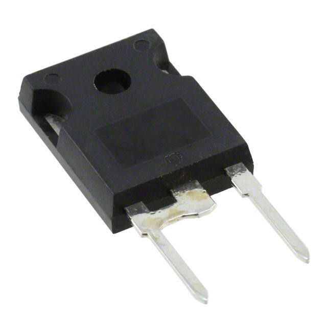
| 描述 | DIODE FAST REC 600V 8A DPAK |
| 产品分类 | 单二极管/整流器 |
| 品牌 | Vishay Semiconductor Diodes Division |
| 数据手册 | |
| 产品图片 |
|
| 产品型号 | VS-8EWH06FNTR-M3 |
| rohs | 无铅 / 符合限制有害物质指令(RoHS)规范要求 |
| 产品系列 | FRED Pt™ |
| 不同If时的电压-正向(Vf) | 2.4V @ 8A |
| 不同 Vr、F时的电容 | - |
| 不同 Vr时的电流-反向漏电流 | 50µA @ 600V |
| 二极管类型 | 标准 |
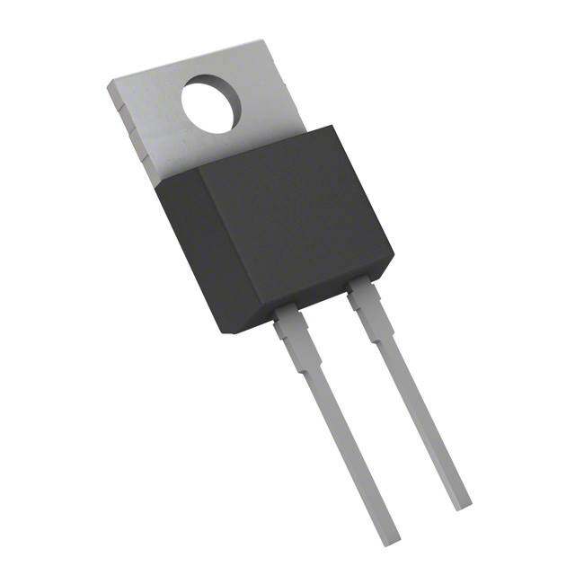
| 供应商器件封装 | D-Pak |
| 其它名称 | VS-8EWH06FNTR-M3TR |
| 包装 | 带卷 (TR) |
| 反向恢复时间(trr) | 25ns |
| 安装类型 | 表面贴装 |
| 封装/外壳 | TO-252-3,DPak(2 引线+接片),SC-63 |
| 工作温度-结 | -65°C ~ 175°C |
| 标准包装 | 2,000 |
| 热阻 | 2.2°C/W Jc |
| 电压-DC反向(Vr)(最大值) | 600V |
| 电流-平均整流(Io) | 8A |
| 速度 | 快速恢复 =< 500 ns,> 200mA(Io) |


- 商务部:美国ITC正式对集成电路等产品启动337调查
- 曝三星4nm工艺存在良率问题 高通将骁龙8 Gen1或转产台积电
- 太阳诱电将投资9.5亿元在常州建新厂生产MLCC 预计2023年完工
- 英特尔发布欧洲新工厂建设计划 深化IDM 2.0 战略
- 台积电先进制程称霸业界 有大客户加持明年业绩稳了
- 达到5530亿美元!SIA预计今年全球半导体销售额将创下新高
- 英特尔拟将自动驾驶子公司Mobileye上市 估值或超500亿美元
- 三星加码芯片和SET,合并消费电子和移动部门,撤换高东真等 CEO
- 三星电子宣布重大人事变动 还合并消费电子和移动部门
- 海关总署:前11个月进口集成电路产品价值2.52万亿元 增长14.8%


PDF Datasheet 数据手册内容提取
VS-8EWH06FN-M3 www.vishay.com Vishay Semiconductors Hyper Fast Rectifier, 8 A FRED Pt® FEATURES • Hyper fast recovery time, reduced Q and soft rr 4 2, 4 recovery • 175 °C maximum operating junction temperature • For PFC CRM/CCM operation 2 • Low forward voltage drop 3 1 3 1 N/C Anode • Low leakage current DPAK (TO-252AA) • Meets MSL level 1, per J-STD-020, LF maximum peak of 260 °C • Material categorization: for definitions of compliance please see www.vishay.com/doc?99912 PRIMARY CHARACTERISTICS DESCRIPTION / APPLICATIONS Package DPAK (TO-252AA) State of the art hyper fast recovery rectifiers designed with IF(AV) 8 A optimized performance of forward voltage drop, hyperfast V 600 V recovery time, and soft recovery. R The planar structure and the platinum doped life time V at I 1.3 V F F control guarantee the best overall performance, ruggedness trr (typ.) 18 ns and reliability characteristics. TJ max. 175 °C These devices are intended for use in PFC boost stage in the Circuit configuration Single die AC/DC section of SMPS inverters or as freewheeling diodes. Their extremely optimized stored charge and low recovery current minimize the switching losses and reduce over dissipation in the switching element and snubbers. ABSOLUTE MAXIMUM RATINGS PARAMETER SYMBOL TEST CONDITIONS VALUES UNITS Peak repetitive reverse voltage V 600 V RRM Average rectified forward current I T = 143 °C 8 F(AV) C Non-repetitive peak surge current I T = 25 °C 90 A FSM J Peak repetitive forward current I T = 143 °C, f = 20 kHz, d = 50 % 16 FM C Operating junction and storage temperatures T , T -55 to +175 °C J Stg ELECTRICAL SPECIFICATIONS (T = 25 °C unless otherwise specified) J PARAMETER SYMBOL TEST CONDITIONS MIN. TYP. MAX. UNITS Breakdown voltage, V , BR I = 100 μA 600 - - blocking voltage V R R V I = 8 A - 2.0 2.4 F Forward voltage V F I = 8 A, T = 150 °C - 1.3 1.8 F J V = V rated - - 50 R R Reverse leakage current I μA R T = 150 °C, V = V rated - - 500 J R R Junction capacitance C V = 600 V - 8 - pF T R Series inductance L Measured lead to lead 5 mm from package body - 8 - nH S Revision: 06-Jun-17 1 Document Number: 93238 For technical questions within your region: DiodesAmericas@vishay.com, DiodesAsia@vishay.com, DiodesEurope@vishay.com THIS DOCUMENT IS SUBJECT TO CHANGE WITHOUT NOTICE. THE PRODUCTS DESCRIBED HEREIN AND THIS DOCUMENT ARE SUBJECT TO SPECIFIC DISCLAIMERS, SET FORTH AT www.vishay.com/doc?91000
VS-8EWH06FN-M3 www.vishay.com Vishay Semiconductors DYNAMIC RECOVERY CHARACTERISTICS (T = 25 °C unless otherwise specified) J PARAMETER SYMBOL TEST CONDITIONS MIN. TYP. MAX. UNITS I = 1 A, dI /dt = 50 A/μs, V = 30 V 21 F F R I = 1 A, dI /dt = 100 A/μs, V = 30 V - 18 22 F F R Reverse recovery time t ns rr T = 25 °C - 25 - J T = 125 °C - 34 - J Peak recovery current I TJ = 25 °C IdFI =/ d8t A= 200 A/μs - 3.3 - A RRM F TJ = 125 °C VR = 390 V - 4.8 - T = 25 °C - 39 - J Reverse recovery charge Q nC rr T = 125 °C - 90 - J THERMAL - MECHANICAL SPECIFICATIONS PARAMETER SYMBOL TEST CONDITIONS MIN. TYP. MAX. UNITS Maximum junction and storage T , T -55 - 175 °C temperature range J Stg Thermal resistance, R - 1.8 2.2 °C/W junction to case per leg thJC 0.3 g Approximate weight 0.01 oz. Marking device Case style TO-252AA (D-PAK) 8EWH06FN A) 100 1000 nt ( rre T = 175 °C A) 100 TJ = 175 °C u J μ d C 10 nt ( 10 TJ = 150 °C ar re TJ = 125 °C orw Cur 1 TJ = 100 °C F e neous 1 TJ = 125 °C Revers 0.1 TJ T=J 7=5 5 °0C °C stanta TJ = 25 °C I - R 0.01 TJ = 25 °C n -I 0.1 0.001 IF 0.0 0.5 1.0 1.5 2.0 2.5 3.0 3.5 4.0 0 100 200 300 400 500 600 V -Forward Voltage Drop (V) V -Reverse Voltage (V) FM R Fig. 1 - Typical Forward Voltage Drop Characteristics Fig. 2 - Typical Values of Reverse Current vs. Reverse Voltage Revision: 06-Jun-17 2 Document Number: 93238 For technical questions within your region: DiodesAmericas@vishay.com, DiodesAsia@vishay.com, DiodesEurope@vishay.com THIS DOCUMENT IS SUBJECT TO CHANGE WITHOUT NOTICE. THE PRODUCTS DESCRIBED HEREIN AND THIS DOCUMENT ARE SUBJECT TO SPECIFIC DISCLAIMERS, SET FORTH AT www.vishay.com/doc?91000
VS-8EWH06FN-M3 www.vishay.com Vishay Semiconductors 100 F) p e ( c n a cit a p a 10 C n o cti n u J - T C 1 0 100 200 300 400 500 600 V -Reverse Voltage (V) R Fig. 3 - Typical Junction Capacitance vs. Reverse Voltage 10 W) C/ ° e ( D = 0.5 c n 1 da D = 02 e p D = 0.1 m al I D = 0.05 m D = 0.02 r 0.1 Single Pulse e D = 0.01 h (Thermal Resistance) T - C J h Zt 0.01 1E-05 1E-04 1E-03 1E-02 1E-01 1E+00 t -Rectangular Pulse Duration (s) 1 Fig. 4 - Maximum Thermal Impedance Z Characteristics thJC 180 20 C) ° 18 RMS Limit e ( 170 ur W) 16 erat 160 ss ( 14 p o Tem 150 DC wer L 1102 DD == 00..0012 e Case 113400 Sraqteuda rVe Rw aapvpel i(eDd = 0.50) age Po 68 DDD = == 0 00.0..125 Allowabl 120 see note (1) Aver 24 DC D = 0.5 110 0 0 2 4 6 8 10 12 14 0 2 4 6 8 10 12 IF(AV) - Average Forward Current (A) IF(AV) - Average Forward Current (A) Fig. 5 - Maximum Allowable Case Temperature vs. Fig. 6 - Forward Power Loss Characteristics Average Forward Current Revision: 06-Jun-17 3 Document Number: 93238 For technical questions within your region: DiodesAmericas@vishay.com, DiodesAsia@vishay.com, DiodesEurope@vishay.com THIS DOCUMENT IS SUBJECT TO CHANGE WITHOUT NOTICE. THE PRODUCTS DESCRIBED HEREIN AND THIS DOCUMENT ARE SUBJECT TO SPECIFIC DISCLAIMERS, SET FORTH AT www.vishay.com/doc?91000
VS-8EWH06FN-M3 www.vishay.com Vishay Semiconductors 50 350 45 300 8 A, T = 125 °C 40 J 250 C) 35 nC) 200 8 A, TJ = 125 °C t (nrr 30 8 A, T = 25 °C Q (rr 150 25 J 20 100 8 A, TJ = 25 °C 15 50 10 0 100 1000 100 1000 dIFdt (A/μs) dIFdt (A/μs) Fig. 7 - Typical Reverse Recovery Time vs. dI /dt Fig. 8 - Typical Stored Charge vs. dI /dt F F Note (1) Formula used: T = T - (Pd + Pd ) x R ; C J REV thJC Pd = forward power loss = I x V at (I /D) (see fig. 6); F(AV) FM F(AV) Pd = inverse power loss = V x I (1 - D); I at V = rated V REV R1 R R R1 R (3) t I rr F t t a b 0 (4) Q rr (2) IRRM 0.5 IRRM dI /dt (5) (rec)M 0.75 I RRM (1) dIF/dt (1) dIF/dt - rate of change of current (4) Qrr - area under curve defined by trr through zero crossing and IRRM t x I (2) IRRM - peak reverse recovery current Q r r = rr 2RRM (3) t - reverse recovery time measured rr (5) dI /dt - peak rate of change of from zero crossing point of negative (rec)M current during t portion of t going I to point where a line passing b rr F through 0.75 I and 0.50 I RRM RRM extrapolated to zero current. Fig. 9 - Reverse Recovery Waveform and Definitions Revision: 06-Jun-17 4 Document Number: 93238 For technical questions within your region: DiodesAmericas@vishay.com, DiodesAsia@vishay.com, DiodesEurope@vishay.com THIS DOCUMENT IS SUBJECT TO CHANGE WITHOUT NOTICE. THE PRODUCTS DESCRIBED HEREIN AND THIS DOCUMENT ARE SUBJECT TO SPECIFIC DISCLAIMERS, SET FORTH AT www.vishay.com/doc?91000
VS-8EWH06FN-M3 www.vishay.com Vishay Semiconductors ORDERING INFORMATION TABLE Device code VS- 8 E W H 06 FN TRL -M3 1 2 3 4 5 6 7 8 9 1 - Vishay Semiconductors product 2 - Current rating (8 = 8 A) 3 - Circuit configuration: E = single diode 4 - Package identifier: W = D-PAK 5 - H = hyperfast recovery 6 - Voltage rating (06 = 600 V) 7 - FN = TO-252AA 8 - None = tube TR = tape and reel TRL = tape and reel (left oriented) TRR = tape and reel (right oriented) 9 - Environmental digit: -M3 = Halogen-free, RoHS-compliant, and terminations lead (Pb)-free ORDERING INFORMATION (Example) PREFERRED P/N QUANTITY PER T/R MINIMUM ORDER QUANTITY PACKAGING DESCRIPTION VS-8EWH06FN-M3 75 3000 Antistatic plastic tube VS-8EWH06FNTR-M3 2000 2000 13" diameter reel VS-8EWH06FNTRL-M3 3000 3000 13" diameter reel VS-8EWH06FNTRR-M3 3000 3000 13" diameter reel LINKS TO RELATED DOCUMENTS Dimensions www.vishay.com/doc?95627 Part marking information www.vishay.com/doc?95176 Packaging information www.vishay.com/doc?95033 SPICE model www.vishay.com/doc?96114 Revision: 06-Jun-17 5 Document Number: 93238 For technical questions within your region: DiodesAmericas@vishay.com, DiodesAsia@vishay.com, DiodesEurope@vishay.com THIS DOCUMENT IS SUBJECT TO CHANGE WITHOUT NOTICE. THE PRODUCTS DESCRIBED HEREIN AND THIS DOCUMENT ARE SUBJECT TO SPECIFIC DISCLAIMERS, SET FORTH AT www.vishay.com/doc?91000
Outline Dimensions www.vishay.com Vishay Semiconductors D-PAK (TO-252AA) “M” DIMENSIONS in millimeters and inches (5) A Pad layout E A C (3) b3 0.010M C A B c2 0.265MIN. L3 (3) A E1 (6.74) Ø 1 Ø 2 4 4 B 0.245MIN. Seating D1 (6.23) plane D (5) H 0.488 (12.40) 0.409 (10.40) 1 2 3 L4 3 2 1 0.089 MIN. (2) L5 Detail “C” (2.28) b c A 0.06 MIN. b2 (1.524) 0.010M C A B 2 xe 0.093 (2.38) Detail “C” (L1) 0.085 (2.18) Rotated 90 °CW Scale: 20:1 Lead tip H (7) Gauge C plane C Seating C plane L2 Ø L A1 MILLIMETERS INCHES MILLIMETERS INCHES SYMBOL NOTES SYMBOL NOTES MIN. MAX. MIN. MAX. MIN. MAX. MIN. MAX. A 2.18 2.39 0.086 0.094 e 2.29 BSC 0.090 BSC A1 - 0.13 - 0.005 H 9.40 10.41 0.370 0.410 b 0.64 0.89 0.025 0.035 L 1.40 1.78 0.055 0.070 b2 0.76 1.14 0.030 0.045 L1 2.74 BSC 0.108 REF. b3 4.95 5.46 0.195 0.215 3 L2 0.51 BSC 0.020 BSC c 0.46 0.61 0.018 0.024 L3 0.89 1.27 0.035 0.050 3 c2 0.46 0.89 0.018 0.035 L4 - 1.02 - 0.040 D 5.97 6.22 0.235 0.245 5 L5 1.14 1.52 0.045 0.060 2 D1 5.21 - 0.205 - 3 Ø 0° 10° 0° 10° E 6.35 6.73 0.250 0.265 5 Ø1 0° 15° 0° 15° E1 4.32 - 0.170 - 3 Ø2 25° 35° 25° 35° Notes (1) Dimensioning and tolerancing as per ASME Y14.5M-1994 (2) Lead dimension uncontrolled in L5 (3) Dimension D1, E1, L3 and b3 establish a minimum mounting surface for thermal pad (4) Section C - C dimension apply to the flat section of the lead between 0.13 and 0.25 mm (0.005 and 0.10") from the lead tip (5) Dimension D, and E do not include mold flash. Mold flash shall not exceed 0.127 mm (0.005") per side. These dimensions are measured at the outermost extremes of the plastic body (6) Dimension b1 and c1 applied to base metal only (7) Datum A and B to be determined at datum plane H (8) Outline conforms to JEDEC® outline TO-252AA Revision: 24-Jun-16 1 Document Number: 95627 For technical questions within your region: DiodesAmericas@vishay.com, DiodesAsia@vishay.com, DiodesEurope@vishay.com THIS DOCUMENT IS SUBJECT TO CHANGE WITHOUT NOTICE. THE PRODUCTS DESCRIBED HEREIN AND THIS DOCUMENT ARE SUBJECT TO SPECIFIC DISCLAIMERS, SET FORTH AT www.vishay.com/doc?91000
Legal Disclaimer Notice www.vishay.com Vishay Disclaimer ALL PRODUCT, PRODUCT SPECIFICATIONS AND DATA ARE SUBJECT TO CHANGE WITHOUT NOTICE TO IMPROVE RELIABILITY, FUNCTION OR DESIGN OR OTHERWISE. Vishay Intertechnology, Inc., its affiliates, agents, and employees, and all persons acting on its or their behalf (collectively, “Vishay”), disclaim any and all liability for any errors, inaccuracies or incompleteness contained in any datasheet or in any other disclosure relating to any product. Vishay makes no warranty, representation or guarantee regarding the suitability of the products for any particular purpose or the continuing production of any product. To the maximum extent permitted by applicable law, Vishay disclaims (i) any and all liability arising out of the application or use of any product, (ii) any and all liability, including without limitation special, consequential or incidental damages, and (iii) any and all implied warranties, including warranties of fitness for particular purpose, non-infringement and merchantability. Statements regarding the suitability of products for certain types of applications are based on Vishay’s knowledge of typical requirements that are often placed on Vishay products in generic applications. Such statements are not binding statements about the suitability of products for a particular application. It is the customer’s responsibility to validate that a particular product with the properties described in the product specification is suitable for use in a particular application. Parameters provided in datasheets and / or specifications may vary in different applications and performance may vary over time. All operating parameters, including typical parameters, must be validated for each customer application by the customer’s technical experts. Product specifications do not expand or otherwise modify Vishay’s terms and conditions of purchase, including but not limited to the warranty expressed therein. Except as expressly indicated in writing, Vishay products are not designed for use in medical, life-saving, or life-sustaining applications or for any other application in which the failure of the Vishay product could result in personal injury or death. Customers using or selling Vishay products not expressly indicated for use in such applications do so at their own risk. Please contact authorized Vishay personnel to obtain written terms and conditions regarding products designed for such applications. No license, express or implied, by estoppel or otherwise, to any intellectual property rights is granted by this document or by any conduct of Vishay. Product names and markings noted herein may be trademarks of their respective owners. © 2017 VISHAY INTERTECHNOLOGY, INC. ALL RIGHTS RESERVED Revision: 08-Feb-17 1 Document Number: 91000
Mouser Electronics Authorized Distributor Click to View Pricing, Inventory, Delivery & Lifecycle Information: V ishay: VS-8EWH06FNTR-M3 VS-8EWH06FN-M3 VS-8EWH06FNTRL-M3 VS-8EWH06FNTRR-M3