ICGOO在线商城 > 电路保护 > TVS - 变阻器,MOV > V68MA3B
 Datasheet下载
- 型号: V68MA3B
- 制造商: Littelfuse
- 库位|库存: xxxx|xxxx
- 要求:
| 数量阶梯 | 香港交货 | 国内含税 |
| +xxxx | $xxxx | ¥xxxx |
查看当月历史价格
查看今年历史价格
V68MA3B产品简介:
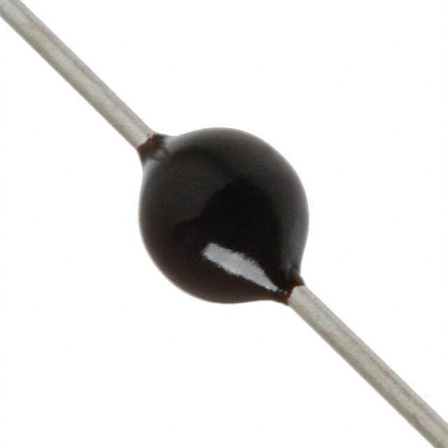
ICGOO电子元器件商城为您提供V68MA3B由Littelfuse设计生产,在icgoo商城现货销售,并且可以通过原厂、代理商等渠道进行代购。 V68MA3B价格参考。LittelfuseV68MA3B封装/规格:TVS - 变阻器,MOV, 68V 40A Varistor 1 Circuit Through Hole SOD-83A Axial。您可以下载V68MA3B参考资料、Datasheet数据手册功能说明书,资料中有V68MA3B 详细功能的应用电路图电压和使用方法及教程。
Littelfuse Inc.的型号V68MA3B属于TVS(瞬态电压抑制)变阻器,即MOV(金属氧化物压敏电阻),主要用于电路中的过电压保护。该器件具有响应速度快、可靠性高的特点,适用于多种电子设备和系统中对电压瞬变敏感的场合。

V68MA3B的主要应用场景包括:

1. 电源系统保护:用于交流或直流电源输入端,防止因雷击、电感负载开关或电网波动引起的电压浪涌损坏后级电路。

2. 工业设备:如PLC、变频器、伺服驱动器等工业自动化设备中,用于保护控制电路和电源模块。

3. 通信设备:在路由器、交换机、基站等通信设备中,用于保护电源接口和信号线路免受静电和浪涌损坏。

4. 消费电子产品:例如电视、机顶盒、智能家电等,用于提升整机的电磁兼容性和可靠性。

5. 汽车电子:在车载电源系统或辅助电子模块中,用于抑制因负载突变或静电放电引起的电压尖峰。

该变阻器具备较高的能量吸收能力,适用于中低功率的电路保护需求,常与其他保护器件(如TVS二极管)配合使用,形成多级保护方案,以提升整体系统的稳定性与安全性。
| 参数 | 数值 |
| 产品目录 | |
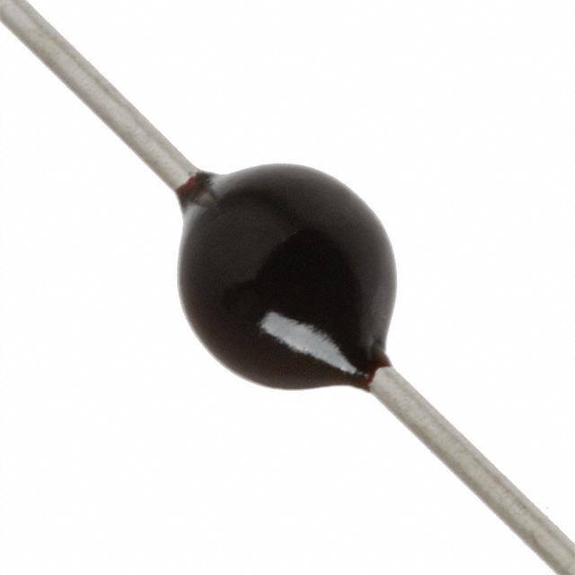
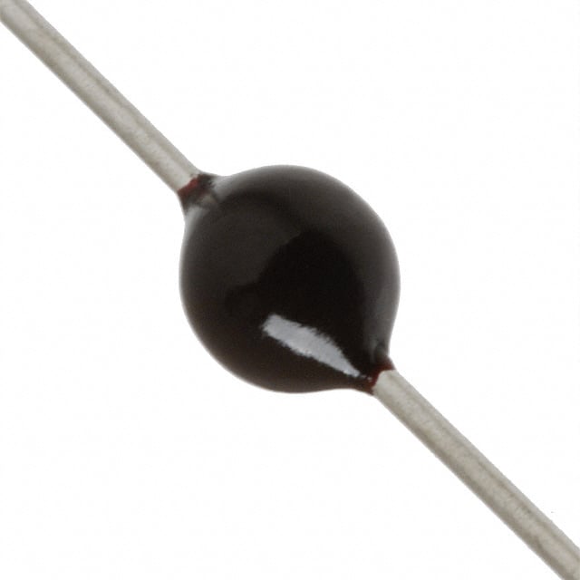
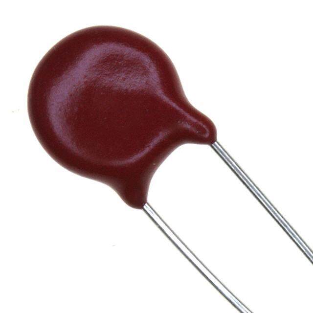
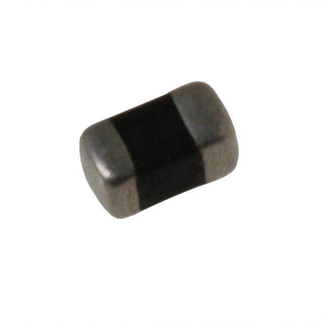
| 描述 | VARISTOR 61V 40A SOD-83A AXIAL压敏电阻 68V 40A 150pF |
| 产品分类 | |
| 品牌 | Littelfuse |
| 产品手册 | |
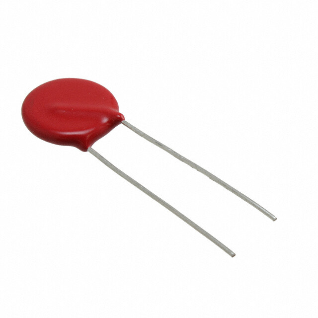
| 产品图片 |
|
| rohs | 符合RoHS无铅 / 符合限制有害物质指令(RoHS)规范要求 |
| 产品系列 | Littelfuse V68MA3BMA |
| 数据手册 | |
| 产品型号 | V68MA3B |
| 产品 | MOV |
| 产品培训模块 | http://www.digikey.cn/PTM/IndividualPTM.page?site=cn&lang=zhs&ptm=25313 |
| 产品目录绘图 |
|
| 产品目录页面 | |
| 产品种类 | 压敏电阻 |
| 其它名称 | F2286 |
| 包装 | 散装 |
| 变阻器电压 | 61V |
| 商标 | Littelfuse |
| 外壳直径 | 3 mm |
| 安装 | Radial |
| 封装 | Bulk |
| 封装/外壳 | SOD-83A,轴向 |
| 尺寸 | 3 mm Dia. |
| 峰值浪涌电流 | 40 A |
| 工作温度范围 | - 55 C to + 85 C |
| 工厂包装数量 | 1500 |
| 最大AC电压 | 40VAC |
| 最大DC电压 | 56VDC |
| 标准包装 | 1,500 |
| 电压额定值AC | 40 V |
| 电压额定值DC | 56 V |
| 电容 | 150 pF |
| 电流-浪涌 | 40A |
| 电路数 | 1 |
| 直径 | 3 mm |
| 端接类型 | Axial |
| 能量 | 0.30J |
| 钳位电压 | 127 V |


- 商务部:美国ITC正式对集成电路等产品启动337调查
- 曝三星4nm工艺存在良率问题 高通将骁龙8 Gen1或转产台积电
- 太阳诱电将投资9.5亿元在常州建新厂生产MLCC 预计2023年完工
- 英特尔发布欧洲新工厂建设计划 深化IDM 2.0 战略
- 台积电先进制程称霸业界 有大客户加持明年业绩稳了
- 达到5530亿美元!SIA预计今年全球半导体销售额将创下新高
- 英特尔拟将自动驾驶子公司Mobileye上市 估值或超500亿美元
- 三星加码芯片和SET,合并消费电子和移动部门,撤换高东真等 CEO
- 三星电子宣布重大人事变动 还合并消费电子和移动部门
- 海关总署:前11个月进口集成电路产品价值2.52万亿元 增长14.8%
PDF Datasheet 数据手册内容提取
Metal-Oxide Varistors (MOVs) Axial Lead / Application Specific Varistors > MA Series MA Varistor Series RoHS Description The MA Series of transient surge suppressors are axial lead Metal Oxide Varistors (MOVs) for use in a wide variety of board level industrial and commercial electronic equipment. They are intended to protect components and signal/data lines from low energy transients where the small axial lead package is required. The MA Series is offered with standard ('S' suffix) or tightened ('B' suffix) clamping voltage. See MA Series Device Ratings and Specifications Table for part number and brand information. Agency Approvals Features Agency Agency File Number • Lead–free, Halogen- • Available in tape and reel or bulk packaging Free and RoHS None • No derating up to compliant. 85ºC ambient • 3mm diameter disc size • New black epoxy offers Additional Information • Small axial lead package improved performance • Wide operating voltage for high temperature range: Lead-free wave V 9V to 264V soldering process. M(AC)RMS Datasheet Resources Samples V 13V to 365V M(DC) Absolute Maximum Ratings • For ratings of individual members of a series, see Device Ratings and Specifications chart Continuous MA Series Units Steady State Applied Voltage: AC Voltage Range (V ) 9 to 264 V M(AC)RMS DC Voltage Range (V ) 13 to 365 V M(DC) Transient: Peak Pulse Current (I ) TM For 8/20µs Current Wave(See Figure 2) 40 to 100 A Single-Pulse Energy Range For 2ms Current Square Wave (W ) 0.06 to 1.7 J TM Operating Ambient Temperature Range (T ) -55 to +85 °C A Storage Temperature Range (T ) -55 to +125 °C STG Temperature Coefficient (αV) of Clamping Voltage (V ) at Specified Test Current <0.01 %/°C C Hi-Pot Encapsulation (COATING Isolation Voltage Capability) 1000 V Dielectric must withstand indicated DC voltage for one minute per MIL-STD 202, Method 301) COATING Insulation Resistance 1000 MΩ CAUTION: Stresses above those listed in “Absolute Maximum Ratings” may cause permanent damage to the device. This is a stress only rating and operation of the device at these or any other conditions above those indicated in the operational sections of this specification is not implied. © 2017 Littelfuse, Inc. Specifications are subject to change without notice. Revised: 09/14/17
Metal-Oxide Varistors (MOVs) Axial Lead / Application Specific Varistors > MA Series MA Series Ratings & Specifications Maximum Rating (85°C) Specifications (25°C) Continuous Transient Max Clamping NuPmarbt er B(mramnd) VRMS VDC (10E/n10er0g0yµ s) CuPerraekn t VarisDtCor T Veostl tCaguerr eant t1mA Vol(t8 V/2C 0aµt s2).0A CaTpyapciitcaanl ce (8/20µs) V V W I Min V Max V f = 1MHz M(AC) M(DC) TM TM N(DC) C (V) (V) (J) (A) (V) (V) (V) (A) (pF) V18MA1A 18A 9 13 0.06 40 14 18 23 49 550 V18MA1B 18B 10 14 0.07 40 15 18 21 44 550 V18MA1S 18S 10 14 0.06 40 15 18 21 49 550 V22MA1A 22A 10 15 0.09 40 16 22 28 55 410 V22MA1B 22B 14 18 0.10 40 19 22 26 51 410 V22MA1S 22S 14 18 0.09 40 19 22 26 55 410 V27MA1A 27A 13 19 0.10 40 21 27 34 67 370 V27MA1B 27B 17 22 0.11 40 24 27 31 59 370 V27MA1S 27S 17 22 0.10 40 24 27 31 67 370 V33MA1A 33A 18 23 0.13 40 26 33 40 73 300 V33MA1B 33B 20 26 0.15 40 29.5 33 36.5 67 300 V33MA1S 33S 20 26 0.14 40 29.5 33 36.5 73 300 V39MA2A 39A 22 28 0.16 40 31 39 47 86 250 V39MA2B 39B 25 31 0.18 40 35 39 43 79 250 V39MA2S 39S 25 31 0.17 40 35 39 43 86 250 V47MA2A 47A 27 34 0.19 40 37 47 57 99 210 V47MA2B 47B 30 38 0.21 40 42 47 52 90 210 V47MA2S 47S 30 38 0.19 40 42 47 52 99 210 V56MA2A 56A 32 40 0.23 40 44 56 68 117 180 V56MA2B 56B 35 45 0.25 40 50 56 62 108 180 V56MA2S 56S 35 45 0.23 40 50 56 62 117 180 V68MA3A 68A 38 48 0.26 40 54 68 82 138 150 V68MA3B 68B 40 56 0.30 40 61 68 75 127 150 V68MA3S 68S 40 56 0.27 40 61 68 75 138 150 V82MA3A 82A 45 60 0.33 40 65 82 99 163 120 V82MA3B 82B 50 66 0.37 40 73 82 91 150 120 V82MA3S 82S 50 66 0.34 40 73 82 91 163 120 V100MA4A 100 57 72 0.40 40 80 100 120 200 100 V100MA4B 101 60 81 0.45 40 90 100 110 185 100 V100MA4S 102 60 81 0.42 40 90 100 110 200 100 V120MA1A 120 72 97 0.40 100 102 120 138 220 40 V120MA2B 121 75 101 0.50 100 108 120 132 205 40 V120MA2S 122 75 101 0.46 100 108 120 132 220 40 V150MA1A 150 88 121 0.50 100 127 150 173 255 32 V150MA2B 151 92 127 0.60 100 135 150 165 240 32 V180MA1A 180 105 144 0.60 100 153 180 207 310 27 V180MA3B 181 110 152 0.70 100 162 180 198 290 27 V220MA2A 220 132 181 0.80 100 187 220 253 380 21 V220MA4B 221 138 191 0.90 100 198 220 242 360 21 V270MA2A 270 163 224 0.90 100 229 270 311 460 17 V270MA4B 271 171 235 1.00 100 243 270 297 440 17 V330MA2A 330 188 257 1.00 100 280 330 380 570 14 V330MA5B 331 200 274 1.10 100 297 330 363 540 14 V390MA3A 390 234 322 1.20 100 331 390 449 670 12 V390MA6B 391 242 334 1.30 100 351 390 429 640 12 V430MA3A 430 253 349 1.50 100 365 430 495 740 11 V430MA7B 431 264 365 1.70 100 387 430 473 700 11 NOTE: Average power dissipation of transients not to exceed 200mW. © 2017 Littelfuse, Inc. Specifications are subject to change without notice. Revised: 09/14/17
Metal-Oxide Varistors (MOVs) Axial Lead / Application Specific Varistors > MA Series Power Dissipation Ratings Peak Pulse Current Test Waveform 100 UE 100 UE 90 AL O1 = Virtual Origin of Wave AL 80 K V 90 T = Time From 10% to 90% of Peak D V 70 EA T1 = Virtual Front time = 1.25 • t ENT OF RATE 654000 ERCENT OF P 50 E2x08Tam2ss =p== l eVTT:i12r tF==uoa VVrl iiaTrrnttimuu 8aae/ll 2FTto0rimo µHnesat CtlTfo uiV mrHareealunlfet V W(aImaluvpeeufolsrem D:uration) C 30 P R 10 PE 20 O1 T TIME 10 T1 0-55 50 60 70 80 90 100 110 120 130 140 150 T2 Figure 1 AMBIENT TEMPERATURE (oC) Figure 2 FIGURE 2. PEAK PULSE CURRENT TEST WAVEFORM ShoFuIlGd UtrRanEs 1i.enCtUs RoRccEuNr Tin, E rNapEiRdG sYu cAcNeDss PioOnW, tEhRe DaEveRrAaTgIeN Gpo wer 0 = Virtual Origin of Wave 1 dissipation requCirUeRdV iEs simply the energy (watt-seconds) per T = Time from 10% to 90% of Peak pulse times the number of pulses per second. The power so T = Rise Time = 1.25 x T 1 developed must be within the specifications shown on the T = Decay Time 2 Device Ratings and Specifications table for the specific device. Example - For an 8/20 µs Current Waveform: Furthermore, the operating values need to be derated at high 8µs = T = Rise Time temperatures as shown above. Because varistors can only 1 20µs = T = Decay Time dissipate a relatively small amount of average power they are, 2 therefore, not suitable for repetitive applications that involve substantial amounts of average power dissipation. Repetitive Surge Capability V18MA - V100MA V120MA1A/S - V430MA3A 50 100 21 DV1IS8CM AS1IZAE - 3Vm10m0MA4B 50 2 1 DV1IS2C0M SAIZ1EA 3- mV4m30MA7B 20 10 10 SURGE CURRENT (A) 01.05215 111000234 105106 SURGE CURRENT (A) 021.005215 102 101031401056 INDEFINITE INDEFINITE 0.2 0.2 0.1 0.1 20 100 1,000 10,000 20 100 1,000 10,000 IMPULSE DURATION(μs) IMPULSE DURATION(μs) Figure 3 Figure 4 FIGURE 7. SURGE CURRENT RATING CURVES FOR V18MA FIGURE 8. SURGE CURRENT RATING CURVES FOR SERIES - V100MA SERIES V120MA SERIES - V430MA SERIES NOTE: If pulse ratings are exceeded, a shift of V (at specified current) of more than N(DC) +/-10% could result. This type of shift, which normally results in a decrease of V , may N(DC) result in the device not meeting the original published specifications, but it does not prevent the device from continuing to function, and to provide ample protection. © 2017 Littelfuse, Inc. Specifications are subject to change without notice. Revised: 09/14/17
800 4,000 MAX CLAMPING VOLTAGE V100MA4A/S MAX CLAMPING VOLTAGE 640000 D1T8AIS T=CO - 5S15I0Zo0ECV 3TNmO(Dm 8C5) oRCATING V8V26M8VAM536AAM3/SAA/2SA/S 2,000 D1T2AIS0 = CT - O5S 5I4Zo3EC0 V3TmON(m D85Co) CRATING V4V330V9M303MA03AMA3AA2A S (V) 300 S (V)1,500 V2V7202M0AM2AA2A OLT 200 OLT1,000 Metal-Oxide VaristoK Vrs15 0(MOVs) K V 800 EA EA 600 Axial Lead / Application SpeM Pc1i0fi0c Varistors > MA Series M P U 80 U 400 M M XI 60 V47MA2A/S XI MA V39MA2A/S MA 40 V33MA1A/S 200 V27MA1A/S V180MA1A 30 V22MA1A/S V150MA1A V18MA1A/S V120MA1A/S 20 100 10-2 10-1 100 101 102 10-2 10-1 100 101 102 PEAK AMPERES (A) PEAK AMPERES (A) Maximum Clamping Voltage FIGURE 3. CLAMPING VOLTAGE FOR V18MA1A/S - V100MA4A/S FIGURE 4. CLAMPING VOLTAGE FOR V120MA1A/S - V430MA3A V18MA1A/S - V100MA4A/S V18MA1B - V100MA4B 800 4,000 MAXIMUM PEAK VOLTS (V) 86432110500000864300000000000 MD1T8AIAS T=XCMAXIMUM PEAK VOLTS (V)O - C 5S1L5I0643211ZAo00500008643ECM0V000000000 3TPNmOI(NDm MD1T8CG8A5I)A S V oTR=XCOCO A - CL T5S1TL5II0ANZAo0GEGCMV E 3TPNmOI(NDm 8CG5)V VoR1OC0AVL0T8TMVI2AN6MAGGV8V4AE2M5AV326A/2AMSVM73/AS3MAAV31V/2A3SMAV1A91/04AVM/SAS0718/AMMVSVA226M1/AASVA88V42A2/MM5ASVA326AA/2/AMSSVM731/AS3MAAAV31//2A3SMSAVA91/4AM/SAS71/AMSA2/ASA2/SA/SMAXIMUM PEAK VOLTS (V)4211,,,,005086420000000000000000 MD1T2AIAMAXIMUM PEAK VOLTS (V)S0MAXIMUM PEAK VOLTS (V) =X CT 654321- OC2115S0000009876543,,,L 5I005086420000000000004ZAo00000003ECM00000000 V3TPmMD1TONIN8A(Im AMD1TDS8 G T=2AX5CCIAO S0 V o)- =CX C 5SOCTR1 L5-I OC0LAZ5SAoT0L T5EICM4AVZAoI 3 NG3ETPNCM0mGO EI( V3NTPDm mON8CIGN5()m D8 GVoR5COC VAVo)L TOC4VRTI3LA3NA0VT9GTGMA30IEVNG3MA20GVE3VA7M1AV2305A12AM0820MA0AM2MVAAA41VA23A31A0V9AVM30VVV13MAV82120V3VVAM2227M1AVM730230VA5A1M3M2AVMA301V82M049AAMBA10AM5VVV7MAB112MA6M186AB1AAAM1028AB2A/2A0MMSA1A2BMA2AABBA334BBB MAXIMUM PEAK VOLTS (V)4321,,,,000098765432000000000000000000000000 MD1T2AIAS0 =X CT I- OM5S 5UI4ZoM3EC0 CV3TmONLA(m D8M5CPo) CIRNAGT VINOGLTAGE VVVVVVVV433221118523937200000000MMMMMMMMAAAAAAAA32276544BBBBBBBB 2010-2 20101-02-1 1100-10 PEAVK1 8AMM1AP011E00AR1/SES (A) 110012 102 10100-2 21010010-031-02-1 10-2 1100-1010-1PEAKV A11M2100P001ME00AR11EAS/ S(A10)1 110012102 110032 10010-3 10-2 10-1 100 101 102 103 Figure 5 PEAK AMPERES (A) PEAK AMPPEERAEKS A(AM)PERES (A) PEAK AMPERES (A) Figure 6 FIGURE 3. CLAMPING VOLTAGE FOR V18MA1A/S - V100MA4A/S FIGURE 4. CLAMPING VOLTAGE FOR V120MA1A/S - FIGURE 5. CLAMPING VOLTAGE FOR V18MA1B - V100MA4B FIGURE 6. CLAMPING VOLTAGE FOR V120MA2B - V430MA7B FIGURE 3. CLAMPING VOLTAGE FOR V18MA1A/S - V100MA4A/S FIGURE 4. CLAMPING VVO4L3T0AMGAE3 FAOR V120MA1A/S - V120MA1A/S - V430MA3A V120MA2VB4 3-0 VM4A330AMA7B MAXIMUM PEAK VOLTS (V) 86432110500000864300000000000 MD1T8AIAS T=XCO - C 5S1L5I0ZAo0ECMV 3TPNmOI(NDm 8CG5) VoROCALTTIANGGE V10V08MVV26M1AV88V4A2MM5AV326AA/2AMSVM731/AS3MAAAV31//2A3SMSAVA91/4AM/SAS71/AMSA2/ASA2/SA/S MAXIMUM PEAK VOLTS (V)MAXIMUM PEAK VOLTS (V)4211654321,,,,00050864200000987654300000000000000000000000000000 MD1TMD1T8AIA2AS I ATS=0X CO=XMAXIMUM PEAK VOLTS (V) C T- C 5S- OC15SL5654321I0LZ 5A0Io00000987654340ZAoE0C000000000000M3VECM 0 3TPN V3TPmOI(mNDONIm NMD1T8C(Gm D88AG5I)A S 5CV oTR =XVoC)OCO AO C-R CL T5S1LTAL5IIT0ANZTAoA0GEIGCMNVG E 3TPGNEmOI(NDm 8CG5) VoRVOCA4VLT33TI0VA9NM30GGVV3MAVE120V3VVA227M1AVV2202305AM713M2AMV082M30VA3AMAV0AMM49A112M5AVVV7MAAB1AA6M1186AB12/AM0A28S1BAA20MMAA2BM2AAVBBAV331V48BB2VBM22M73VAM3VA31VM49AB15VVV7MAB16M186B1AM028BA20MMA2BM2AABBA334BBB MAXIMUM PEAK VOLTS (V)4321,,,,000098765432000000000000000000000000 MD1T2AIAS0 MAXIMUM PEAK VOLTS (V)=X CT I- OM43215S,,,, 5UI0000987654324Zo000000000000M3EC0000000000000 CV3TmONLA(m MD1TD8M2A5CIAS0P o)=X CCITR NI- OMA5SG T5UI4 ZoVIM3NECO0G CV3LTTmONLAA(m DG8M5CEPo) CIRNAGT VINOGLTAGE VVVVVVVV433221118523937200000000MMMMMMMMAAAAAAAA32276544BBBBBBBB VVVVVVVV433221118523937200000000MMMMMMMMAAAAAAAA32276544BBBBBBBB 2010-2 10-1 PEAK AM1P0E0RES (A) 101 102 Figure 7120011000--32 102-20101-30-110P-1E1A0K-2 AM11P00E00PR1E0EA-S1K ( AA1)MV01P18E1MR01A0E011SB (A10)2101 110023102 103 10010-3 101-02010-3 10-110-2 10010P-1EAK10 A1M1P0E0RE1S0 2(A1)01 103102 103 PEAK AMPERES (A) Figure 8 PEAK AMPERES (A) FIGURE 3. CLAMPING VOLTAGE FOR V18MA1A/S - V100MA4A/S FIGURE 4. CFLIGAUMRPEIN 5G. VCOLLATMAPGIEN GFO VRO VLT1A2G0ME AF1OAR/S V -1 8MA1B - V100MA4B FIGURE 6. CLAMPING VOLTAGE FOR V120MA2B - V430MA7B FIGURE 5. CLAMPING VOLTAGE FOR V18MA1B - V100MA4B FIGURE 6. CLAMPING VOLTAGE FOR V120MA2B - V430MA7B V430MA3A Wave Solder Profile 600 4,000 500 MAX CLAMPING VOLTAGE Non Lead–fMreAXeIM PUrMo CfiLAleMPING VOLTAGE Lead–free Profile 430000 D1T8AIS T=CO - 5S15I0Zo0ECV 3TNmO(Dm 8C5) oRCATING VV18020MMAA34BB 32,,000000 D1T2AIS0 = CT - O5S 5I4Zo3EC0 V3TmON(m D85Co) CRATING MAXIMUM PEAK VOLTS (V)210098765400000000 V3V3V3VM495V7MA6M61AM8BA2MA2B2ABB3B ERATURE (ºC) MAXIMUM PEAK VOLTS (V)312205051,0000098765432000000000000000000 Maximum WaveVVVVVVVV 433221112852393724000000000MMMMMMMMCAAAAAAAA32276544BBBBBBBB ERATURE (ºC) 312205050000 Maximum Wave 260C 30 VV1V82M22M7AMA1AB1B1B TEMP 100 TEMP 100 20 100 10-3 10-2 10-1 100 101 102 103 50 10-3 10-2 10-1 100 101 102 103 50 PEAK AMPERES (A) PEAK AMPERES (A) 0 0 FIGURE 5. CLAMPING VOLTAGE FOR V18MA1B - V100MA4B FIGURE 6. CLAMPING VOLTAGE FOR V120MA2B - V430MA7B 0 0.5 1 1.5 2 2.5 3 3.5 4 0 0.5 1 1.5 2 2.5 3 3.5 4 Figure 9 TIME(MINUTES) Figure 10 TIME(MINUTES) © 2017 Littelfuse, Inc. Specifications are subject to change without notice. Revised: 09/14/17
Metal-Oxide Varistors (MOVs) Axial Lead / Application Specific Varistors > MA Series Product Dimensions Physical Specifications Lead Material Tin–plated Copper clad steel L L D (diameter) Soldering Solderability per MIL–STD–202, Characteristics Method 208 b (diameter) H Cured, flame retardant epoxy polymer Insulating Material meets UL94V–0 requirements Inches Millimeters Device Labeling Marked with LF, voltage and date code Symbol Min Max Min Max Øb 0.024 0.026 0.61 0.66 H Environmental Specifications ØD 0.118 0.177 3.0 4.5 øb H 0.177 0.276 4.5 7.0 L L Operating/Storage øD -40°C to +85°C L 1.740 1.220 2D7. 3(diameter) 31.0 Temperature Typical Weight = 0.5g b (diameter) H +85°C, 1000 hours L G L Passive Aging +/-10% typical voltage change Tape and Reel Dimensions +85°C, 85% RH, 1000 hours Humidity Aging +/-10% typical voltage change H1 = H2 +/- 0.040” H1 H2 +85°C to -40°C 5 times 0.063” max Thermal Shock +/-10% typical voltage change Solvent Resistance MIL–STD–202, Method 215 0.200” +/- 0.02 Moisture Sensitivity Level 1, J-STD-020 Part Numbering System 0.080” max V XXX MA XX 0.240”+/- 0.040 VARISTOR ENERGY/CLAMPING 2.062”+/- 0.059 VOLTAGE VARIANT 2.681” max VARISTOR VOLTAGE SERIES DESIGNATOR Conforms to EIA Standard RS-296-E (VN at 1mA) MA: Bulk Pack MT: Tape and Reel H1 = H2 0.040 0M.0A6X3 H1 H2 0M.0A6X3 0.098- 0.177 0.135- 0.145 0.02- 0.023 0.200 0.020 0.118- 0.236 0.080 Disclaimer Notice - Information furnished is believed MtAoX be accurate and reliable. However, users should independently evaluate the suitability of and test each product selected for their own applications. Littelfuse products are not designed for, and may not be used in, all applications. Read complete Disclaimer Notice at www.littelfuse.com/disclaimer-electronics. 0.240 2.062 0.240 0.040 0.059 0.040 © 2017 Littelfuse, Inc. Specifications are subject to change without n2.o6t8i1ce. MAX Revised: 09/14/17 •Conforms to EIA Standard RS-296E