ICGOO在线商城 > 电路保护 > TVS - 变阻器,MOV > V510SM7
 Datasheet下载
- 型号: V510SM7
- 制造商: Littelfuse
- 库位|库存: xxxx|xxxx
- 要求:
| 数量阶梯 | 香港交货 | 国内含税 |
| +xxxx | $xxxx | ¥xxxx |
查看当月历史价格
查看今年历史价格
V510SM7产品简介:
ICGOO电子元器件商城为您提供V510SM7由Littelfuse设计生产,在icgoo商城现货销售,并且可以通过原厂、代理商等渠道进行代购。 V510SM7价格参考。LittelfuseV510SM7封装/规格:TVS - 变阻器,MOV, 822.5V 1.2kA Varistor 1 Circuit 表面贴装,MLCV 2-SMD,J 形引线。您可以下载V510SM7参考资料、Datasheet数据手册功能说明书,资料中有V510SM7 详细功能的应用电路图电压和使用方法及教程。
Littelfuse Inc. 的 V510SM7 是一款高能量瞬态电压抑制(TVS)压敏电阻(MOV),主要用于过压保护。其额定电压为510V AC,适用于交流电源线路中的浪涌保护。该器件典型应用于工业设备、电源系统、家用电器和电信基础设施中,用于防护因雷击、开关瞬态或电网波动引起的电压浪涌。

V510SM7 常见于交流输入端口,如开关电源、不间断电源(UPS)、电表、电机驱动器和配电箱等设备中,能有效吸收突发的高能量脉冲,保护后级敏感电子元件免受损坏。其大通流能力和高可靠性使其适合在严苛环境和长期运行条件下使用。

此外,该型号符合多项国际安全标准,具备良好的耐久性和稳定性,广泛用于需要符合IEC、UL等认证要求的终端产品中。总体而言,V510SM7 适用于各类需交流电源浪涌保护的中高压应用场景。
| 参数 | 数值 |
| 产品目录 | |
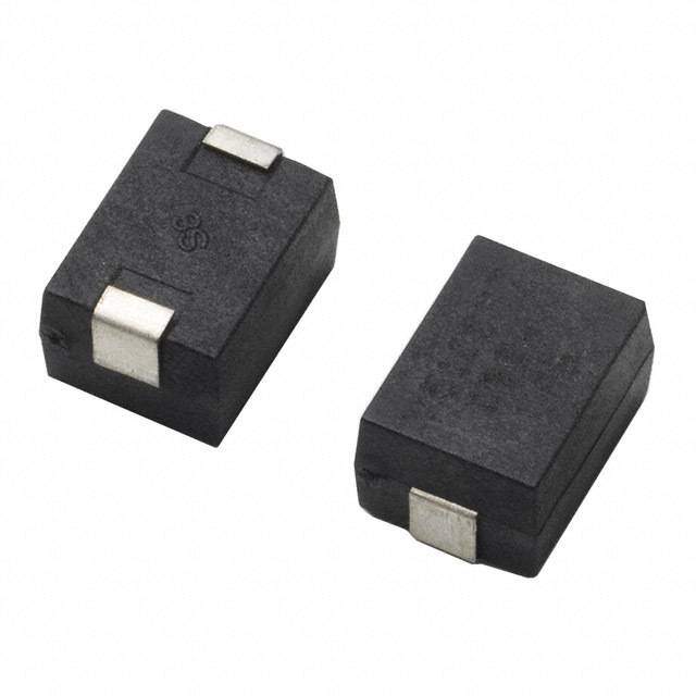
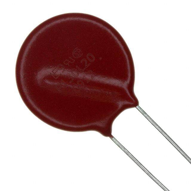
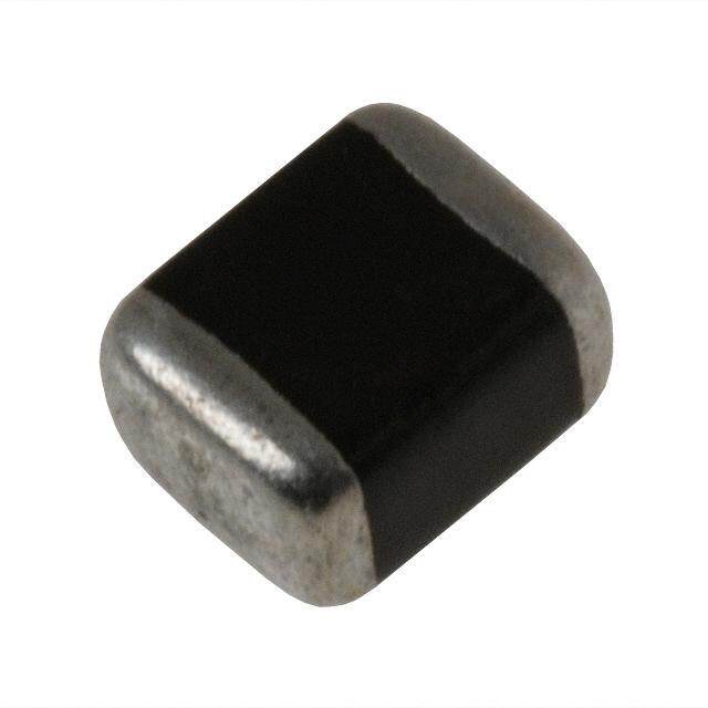
| 描述 | VARISTOR 735V 1.2KA 2-SMD J-LEAD压敏电阻 SURFACE MOUNT SM7 VARISTORS |
| 产品分类 | |
| 品牌 | Littelfuse |
| 产品手册 | |
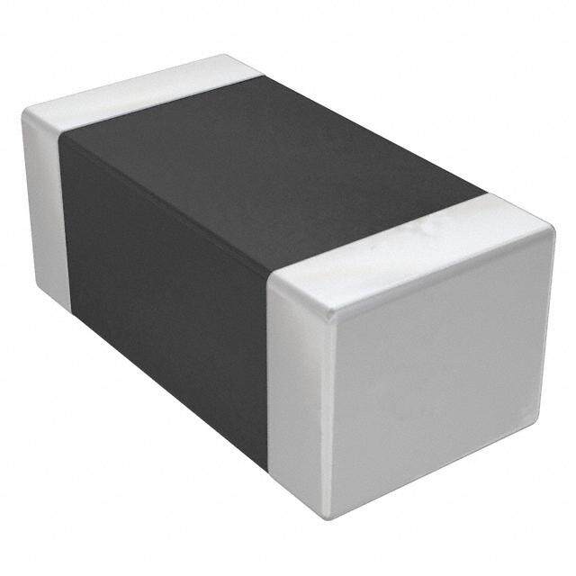
| 产品图片 |
|
| rohs | 符合RoHS无铅 / 符合限制有害物质指令(RoHS)规范要求 |
| 产品系列 | Littelfuse V510SM7SM7 |
| 数据手册 | |
| 产品型号 | V510SM7 |
| 产品培训模块 | http://www.digikey.cn/PTM/IndividualPTM.page?site=cn&lang=zhs&ptm=25313http://www.digikey.cn/PTM/IndividualPTM.page?site=cn&lang=zhs&ptm=25936 |
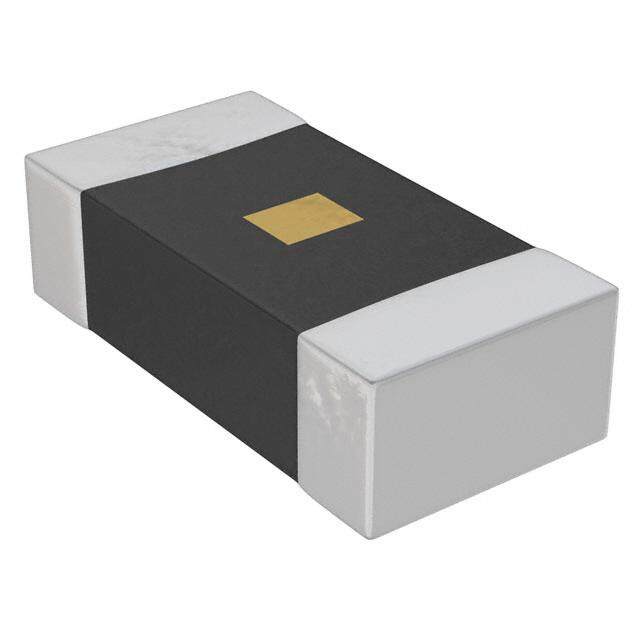
| 产品目录绘图 |
|
| 产品目录页面 | |
| 产品种类 | 压敏电阻 |
| 其它名称 | F3557DKR |
| 包装 | 带卷 (TR) |
| 变阻器电压 | 735V |
| 商标 | Littelfuse |
| 安装 | SMD/SMT |
| 封装 | Reel |
| 封装/外壳 | 2-SMD,J 形引线 |
| 峰值浪涌电流 | 1.2 kA |
| 工作温度范围 | - 40 C to + 85 C |
| 工厂包装数量 | 600 |
| 最大AC电压 | 510VAC |
| 最大DC电压 | 675VDC |
| 标准包装 | 1 |
| 电压额定值AC | 510 V |
| 电压额定值DC | 675 V |
| 电容 | 45 pF |
| 电流-浪涌 | 1.2kA |
| 电路数 | 1 |
| 能量 | 40J |
| 钳位电压 | 1.2 kV |


- 商务部:美国ITC正式对集成电路等产品启动337调查
- 曝三星4nm工艺存在良率问题 高通将骁龙8 Gen1或转产台积电
- 太阳诱电将投资9.5亿元在常州建新厂生产MLCC 预计2023年完工
- 英特尔发布欧洲新工厂建设计划 深化IDM 2.0 战略
- 台积电先进制程称霸业界 有大客户加持明年业绩稳了
- 达到5530亿美元!SIA预计今年全球半导体销售额将创下新高
- 英特尔拟将自动驾驶子公司Mobileye上市 估值或超500亿美元
- 三星加码芯片和SET,合并消费电子和移动部门,撤换高东真等 CEO
- 三星电子宣布重大人事变动 还合并消费电子和移动部门
- 海关总署:前11个月进口集成电路产品价值2.52万亿元 增长14.8%
PDF Datasheet 数据手册内容提取
Metal-Oxide Varistors (MOVs) Surface Mount Varistors > SM7 Series SM7 Varistor Series RoHS Description The Littelfuse SM7 is a plastic-encapsulated surface mount MOV in a PPS material molded package with tin-plated terminal which is fully qualified in lead free soldering and available for both reflow and wave soldering process. SM7 is constructed with 7mm varistor element disc. Its maximum operating ambient temperature is 85ºC with peak pulse current of 1200A. Features • Electrical equivalent • Good solderability to leaded types • Available in tape Agency Approvals LA/ZA series and reel • AC Voltage Rating Agency Agency Approval Agency File Number • Application of AC 50 to 510VAC rms power meters UL1449 E320116 • No De-Rating up • Lead free and to 85°C ambient RoHS compliant Absolute Maximum Ratings • For ratings of individual members of a series, see Device Ratings and Specifications chart Continuous SM7 Series Units Steady State Applied Voltage: AC Voltage Range (V ) 50 to 510 V M(AC)RMS DC Voltage Range (V ) 68 to 675 V M(DC) Transients: Peak Pulse Current (I ) TM For 8/20µs Current Wave (See Figure 2) 1200 A Single Pulse Energy Range For 10/1000µs Current Wave (W ) 10 to 40 J TM Operating Ambient Temperature Range (T) -40 to +85 OC A Storage Temperature Range (T ) -55 to +125 OC STG Temperature Coefficient (aV) of Clamping Voltage (V) at Specified Test Current <0.01 %/OC C Hi-Pot Encapsulation (COATING Isolation Voltage Capability) 2500 V (Dielectric must withstand indicated DC voltage for one minute per MIL-STD 202, Method 301) COATING Insulation Resistance 1000 MΩ CAUTION: Stresses above those listed in “Absolute Maximum Ratings” may cause permanent damage to the device. This is a stress only rating and operation of the device at these or any other conditions above those indicated in the operational sections of this specification is not implied. Additional Information Datasheet Resources Samples © 2017 Littelfuse, Inc. Specifications are subject to change without notice. Revised: 09/14/17
Metal-Oxide Varistors (MOVs) Surface Mount Varistors > SM7 Series SM7 Series Ratings & Specifications Maximum Rating (85°C) Specifications (25°C) Continuous Transient Varistor Voltage Maximum Clamping Typical Energy Peak Current at 1mA DC Voltage Capacitance V V RMS DC 10 x 1000µs 8 x 20µs Test Current 8 x 20 µs f = 1MHz Part V V W I V Min V Max V I C M(AC) M(DC) TM TM NOM NOM C PK Number (V) (V) (J) (A) (V) (V) (V) (A) (pF) V50SM7 50 68 4 1200 73 91 135 10 700 V60SM7 60 81 5 1200 90 110 165 10 600 V115SM7 115 153 10 1200 162 198 300 10 200 V130SM7 130 175 11 1200 184 228 340 10 180 V140SM7 140 180 12 1200 198 242 360 10 160 V150SM7 150 200 13 1200 212 268 395 10 150 V175SM7 175 225 15 1200 247 303 455 10 130 V230SM7 230 300 20 1200 324 396 595 10 100 V250SM7 250 330 21 1200 354 429 650 10 90 V275SM7 275 369 23 1200 389 473 710 10 80 V300SM7 300 405 25 1200 420 517 775 10 70 V320SM7 320 420 25 1200 462 565 850 10 65 V385SM7 385 505 27 1200 558 682 1025 10 60 V420SM7 420 560 30 1200 610 748 1120 10 55 V460SM7 460 615 37 1200 640 790 1190 10 55 V480SM7 480 640 35 1200 670 825 1240 10 50 V510SM7 510 675 40 1200 735 910 1200 10 45 Product Dimensions Part Numbering System 11.4±0.3 8.3±0.3 V 275 SM7 3.6+/-0.3 for x a V50SM7-V60SM7 m 3 6.0+/-0.3 for For “VARISTOR” 0. V115SM7 to V510SM7 VM(AC) 1.5±0.3 3.0±0.3 (Three digits -- 115V to 510V) 6.5 3.5 All dimensions shown SM7 SERIES in milimeters 13.1 Soldering Pad Layout © 2017 Littelfuse, Inc. Specifications are subject to change without notice. Revised: 09/14/17
Metal-Oxide Varistors (MOVs) Surface Mount Varistors > SM7 Series Lead (Pb) Soldering Recommendations The principal techniques used for the soldering of Reflow Solder Profile components in surface mount technology are IR Re-flow and Wave soldering. Typical profiles are shown on the right. 225500 The terminals of SM7 series devices are tin plated copper, MMAAXXIIMMUUMM TTEEMMPPEERRAATTUURREE and the recommended solder is 62/36/2 (Sn/Pb/Ag), 60/40 223300°°CC 222005000 (Sn/Pb) or 63/37 (Sn/Pb). Littelfuse also recommends an 4400--8800 CC MAXIMUM TEMPERATSSUEERCCEOONNDDSS RMA solder flux. RE °RE ° 211055000 230°C AABBOOVVEE 118833°°CC WTthoea avrvmeo asidlo sltdhheoerc ipnko,g sa is spi btrheiliehty em aotof ssgttea sngteerer ianntu itnohgue ss s toorefl dstehsreeins p gdr oupcereo tscose esss. TEMPERATUTEMPERATUATURE °C 111005000 PPRREEHHEEAATT DDWWEELLR<R<RLL22AAA°°MMMCCPP//Pss RRRAAAABSTTTOEEEE4CV0EO-8 N108D3S°C R <2°C/s is recommended, and the peak temperature of the solder PE 1055000 PPRREEHHEEAATT ZZOONNEE process should be rigidly controlled. EM PREHEAT DWELL T 5000 PREHEAT ZONE When using a reflow process, care should be taken to 00 00..55 11..00 11..55 22..00 22..55 33..00 33..55 44..00 ensure that the SM7 chip is not subjected to a thermal TTIIMMEE ((MMIINNUUTTEESS)) 0 gradient steeper than 4 degrees per second; the ideal 0 FF 0IIGG.5UU RR EE 1 11.044 .. RR EE 1FF.5LL OO WW SS2.OO0 LL DD EE 2RR.5 PP RR OO FF3.II0LL EE 3.5 4.0 gradient being 2 degrees per second. During the soldering Wave Solder Profile TIME (MINUTES) process, preheating to within 100 degrees of the solder's FIGURE 14. REFLOW SOLDER PROFILE peak temperature is essential to minimize thermal shock. 330000 Once the soldering process has been completed, it is MMAAXXIIMMUUMM WWAAVVEE 226600°°CC still necessary to ensure that any further thermal shocks 225500 300 are avoided. One possible cause of thermal shock is hot CC printed circuit boards being removed from the solder RE °RE ° 222005000 MAXIMUM WAVE 260°C UU ptteorom lecpesessr sat htauanrnde 5.s T0uhºbCeje bbceotefaodrdr etso cm clelueasantni nbingeg. a slloolwveendt sto a tc oroool mgr adually TEMPERATTEMPERATATURE °C 111121005550000000 SSEECCOONNDD PPRREEHHEEAATT R E FFIIRRSSTT PPRREEHHEEAASTTECOND PREHEAT MP 5500 E 100 T 00 FIRST PREHEAT 5000..00 00..55 11..00 11..55 22..00 22..55 33..00 33..55 44..00 44..55 TTIIMMEE ((MMIINNUUTTEESS)) 0 0.0 0FF.5IIGGUURR1.0EE 1155..1.WW5AAVVEE2 .SS0OOLLDD2.EE5RR PPRR3.OO0FFIILL3EE.5 4.0 4.5 TIME (MINUTES) Lead–free (Pb-free) Soldering Recommendations FIGURE 15. WAVE SOLDER PROFILE The terminals of SM7 series devices are tin plated copper, and the recommended Lead-free solder is 96.5/3.0/0.5 Lead–33f00r00ee Re-flow Solder Profile MMAAXXIIMMUUMM TTEEMMPPEERRAATTUURREE 225500˚˚CC,, (SnAgCu) with an RMA flux, though there is a wide TTIIMMEE WWIITTHHIINN 55˚˚CC OOFF PPEEAAKK 225500 2200 SSEECCOONNDDSS MMAAXXIIMMUUMM selection of pastes and fluxes available that should be 300 compatible. RE °CRE °C222005000 MT20IAM SXEEI MWCUOITMNH DTINSE M5M˚PCAE XOR<R<RI33AAFMA˚˚ MMCCTUPU//PPEMssR ARREKAA 2TT5EE0˚C, 6600 >>-- 112255110077 ˚˚SSCCEECC UU iTsnoh tledh ereer iLflneogaw, dt –hpferro eWfiel eaRv meefl uSosowtl d bPeerr o cPfiorlnoesfi. tlFeroa sirn tLeileld aa bdpy–p fltirehesee. mWaaxviem ums TEMPERATTEMPERATATURE °C211111000555000000 PPRREEHHEEAATT ZZOOR<NN3AEE˚MC/Ps RATE 60 >- 125107 ˚SCEC R E Note: the Lead–free paste, flux and profile were used for MP 5500 evaluation purposes by Littelfuse, based upon industry TE100 PREHEAT ZONE standards and practices. There are multiple choices of all 00 5000 11..00 22..00 33..00 44..00 55..00 66..00 77..00 three available, it is advised that the customer explores the TTIIMMEE ((MMIINNUUTTEESS)) optimum combination for their process as processes vary 0 0 FF II GG UU RR1.EE0 11 66 .. LL 2EE.AA0 DD -- FF RR 3EE.EE0 RR EE -- FF4LL.0OO WW SS OO5.LL0DD EE RR PP6.RR0OO FF II LL EE7.0 considerably from site to site. TIME (MINUTES) FIGURE 16. LEAD-FREE RE-FLOW SOLDER PROFILE © 2017 Littelfuse, Inc. Specifications are subject to change without notice. Revised: 09/14/17
Metal-Oxide Varistors (MOVs) Surface Mount Varistors > SM7 Series Peak Pulse Current Test Waveform for Clamping Peak Current, Energy and Power Derating Curve Voltage For applications exceeding 85ºC ambient temperature, the peak surge current and energy ratings must be reduced as shown below st E Te LU100 A V 100 K A ALUE 9800 OF PE 50 D V 70 NT E E RAT 60 ERC OF 50 P 0 NT 40 O t TIME CE 30 1 t1 R PE 20 t 2 10 0 = Virtual Origin of Wave 0 1 -55 50 60 70 80 90 100 110 120 130 140 150 T = Time from 10% to 90% of Peak AMBIENT TEMPERATURE (oC) T = Rise Time = 1.25 x T 1 T = Decay Time 2 FIGURE 1. CURRENT, ENERGY AND POWER DERATING Example - For an 8/20 µs Current Waveform: CURVE 8µs = T = Rise Time V-I Limit Curves 1 20µs = T = Decay Time 2 2000 V510SM7 Pulse Rating Curves V480SM7 V460SM7 V420SM7 1500 V385SM7 V320SM7 10000 V) V300SM7 e( V250SM7 ag1000 V230SM7 olt V210SM7 1000 1 V V190SM7 A) 2 500 VV117550SSMM77 ent ( 10 104 105 VVV111143500SSSMMM777 ge Curr 100 110023 106 0 ur S 0.001 0.01 0.1 1 10 100 1000 Current(A) 10 NOTE: If pulse ratings are exceeded, a shift of VN(DC) (at specified current) of more than 1 ±10% could result. This type of shift, which normally results in a decrease of VN(DC), may 10 100 1000 10000 result in the device not meeting the original published specifications, but it does not prevent Impulse Duration (µs) the device from continuing to function, and to provide ample protection. Physical Specifications Environmental Specifications Operating Ambient Lead Material Folded Tin Plated Metal Leads -40°C to +85°C Temperature Range (T ) A Soldering Storage Temperature J-STD-002 -55°C to 125°C Characteristics Range(T ) STG Molded Plastic Meets UL94 V-0 Coating Solvent Resistance MIL STD 202, Method 215 Requirement Level 1, J-STD-020 (V115SM7 to Moisture Sensitivity V510SM7) Disclaimer Notice - Information furnished is believed to be accurate and reliable. However, users should independently evaluate the suitability of and test each product selected for their own applications. Littelfuse products are not designed for, and may not be used in, all applications. Read complete Disclaimer Notice at www.littelfuse.com/disclaimer-electronics. © 2017 Littelfuse, Inc. Specifications are subject to change without notice. Revised: 09/14/17
Metal-Oxide Varistors (MOVs) Surface Mount Varistors > SM7 Series Tape & Reel Specifications for V50SM7 amd V60SM7 Carrier Tape P0 mm P2 P1 D0 W 16.00±0.30 E T 0.40±0.05 A A B F W 5° A0 11.80±0.10 0 B B0 8.60±0.10 0 B D1 3.6 K0 4.80±0.10 T A0 E 1.75±0.10 B-B 11.30 15° F 7.50±0.10 2 P0 4.00±0.10 0 K P1 16.00±0.10 A-A m P2 2.00±0.10 m 0 4. D0 ø1.50 +0.10/-0 8 - 3. D1 ø1.50 +0.10/-0 Plastic Reel DETAIL H NOTES: 1) All dimensions per EIA-481-c Ø13±0.2 2±0.5Ø21±0.8 2) 1±00 p.2it0chmems cumulative tolerance on tape Ø100 Ø330 R1 3) Quantity per 13 inch (330 mm) reel: 600 pcs 16.5 120° DETAIL H 21.5±0.4 Tape & Reel Specifications for V115SM7 to V510SM7 Carrier Tape mm P0 P2 P1 W 16.00±0.30 D0 T 0.40±0.05 E A A B F A0 11.80±0.10 W 05° B0 8.60±0.10 B K0 6.80±0.10 0 B D1 3.6 E 1.75±0.10 T A0 11.30 B-B F 7.50±0.10 10° 5° P0 4.00±0.10 2 6.2K0 P1 16.00±0.10 P2 2.00±0.10 A-A D0 ø1.50 +0.10/-0 D1 ø1.50 +0.10/-0 Plastic Reel NOTES: DETAIL H 1) All dimensions per EIA-481-c Ø13±0.2 2±0.5Ø21±0.8 23)) 1Q±0u0 pa.2nit0tcihmtye msp ecru 1m3u ilnactihv e(3 t3o0le mramnc)e r eoenl :t 6ap0e0 pcs Ø100 Ø330 R1 16.5 120° DETAIL H 21.5±0.4 © 2017 Littelfuse, Inc. Specifications are subject to change without notice. Revised: 09/14/17