ICGOO在线商城 > 电路保护 > TVS - 变阻器,MOV > V220CH8T
 Datasheet下载
- 型号: V220CH8T
- 制造商: Littelfuse
- 库位|库存: xxxx|xxxx
- 要求:
| 数量阶梯 | 香港交货 | 国内含税 |
| +xxxx | $xxxx | ¥xxxx |
查看当月历史价格
查看今年历史价格
V220CH8T产品简介:
ICGOO电子元器件商城为您提供V220CH8T由Littelfuse设计生产,在icgoo商城现货销售,并且可以通过原厂、代理商等渠道进行代购。 V220CH8T价格参考。LittelfuseV220CH8T封装/规格:TVS - 变阻器,MOV, 220V 250A Varistor 1 Circuit Surface Mount, MLCV 2-SMD, No Lead。您可以下载V220CH8T参考资料、Datasheet数据手册功能说明书,资料中有V220CH8T 详细功能的应用电路图电压和使用方法及教程。
Littelfuse Inc.的型号V220CH8T是一种金属氧化物压敏电阻(MOV),属于TVS(瞬态电压抑制)器件,主要用于电路中的过电压保护。该型号的额定电压为220V,适用于交流电源线路的浪涌保护。

V220CH8T的典型应用场景包括:

1. 电源保护:广泛用于电源适配器、开关电源、不间断电源(UPS)等设备中,抑制因雷击或开关操作引起的瞬态过电压,保护后级电路不受损坏。

2. 家用电器:如空调、洗衣机、冰箱等家电产品中,用于保护控制电路和电机驱动电路免受电压浪涌的影响。

3. 工业设备:应用于工业控制系统、变频器、PLC等设备中,提升系统的稳定性和可靠性。

4. 通信设备:用于通信基站、路由器、交换机等设备的电源输入端,防止外部浪涌对敏感电子元件造成损害。

5. 智能电表与能源管理系统:在智能电网和能源监控系统中,为电路提供可靠的过电压保护。

该器件具有响应速度快、吸收能量大、可靠性高等优点,是电子设备中常用的保护元件。使用时通常并联在被保护电路与地之间,当电压超过其击穿电压时迅速导通,将浪涌能量泄放至地,从而保护后续电路。
| 参数 | 数值 |
| 产品目录 | |
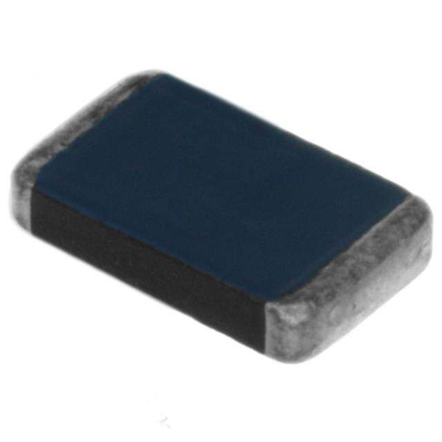
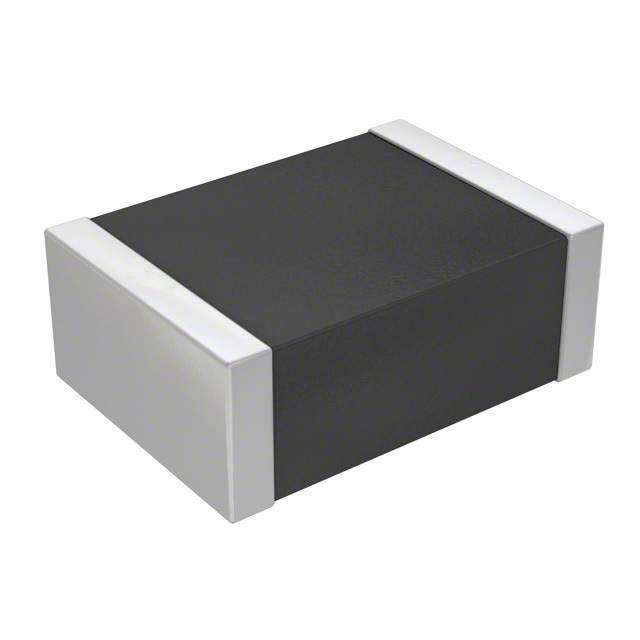
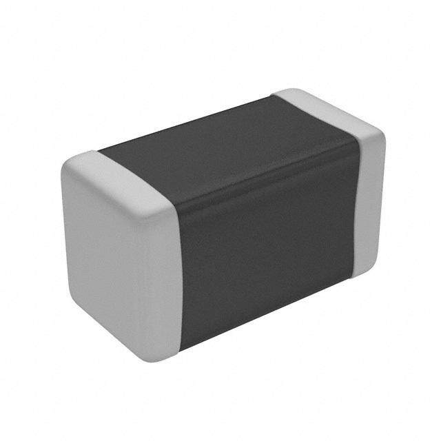
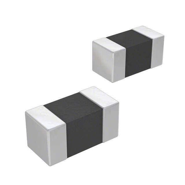
| 描述 | VARISTOR 198V 250A 2-SMD压敏电阻 140V 250A 105pF 7 Inch Reel |
| 产品分类 | |
| 品牌 | Littelfuse |
| 产品手册 | |
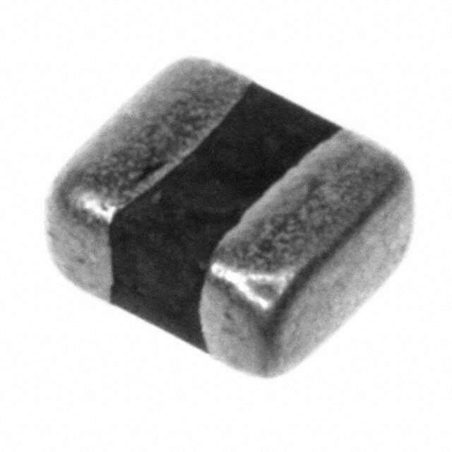
| 产品图片 |
|
| rohs | 符合RoHS不受无铅要求限制 / 符合限制有害物质指令(RoHS)规范要求 |
| 产品系列 | Littelfuse V220CH8TCH |
| 数据手册 | |
| 产品型号 | V220CH8T |
| 产品 | MOV |
| 产品培训模块 | http://www.digikey.cn/PTM/IndividualPTM.page?site=cn&lang=zhs&ptm=25313 |
| 产品目录页面 | |
| 产品种类 | 压敏电阻 |
| 其它名称 | F3462DKR |
| 包装 | Digi-Reel® |
| 变阻器电压 | 220 V |
| 商标 | Littelfuse |
| 外壳代码-in | 3220 |
| 外壳代码-mm | 8552 |
| 外壳宽度 | 5 mm |
| 安装 | SMD/SMT |
| 宽度 | 5 mm |
| 封装 | Reel |
| 封装/外壳 | 2-SMD,无引线 |
| 封装/箱体 | 3220 (8552 metric) |
| 尺寸 | 5 mm W x 8 mm L x 2.03 mm H |
| 峰值浪涌电流 | 250 A |
| 工作温度范围 | - 55 C to + 125 C |
| 工厂包装数量 | 1000 |
| 最大AC电压 | 140VAC |
| 最大DC电压 | 180VDC |
| 标准包装 | 1 |
| 浪涌能量额定值 | 5 J |
| 电压额定值AC | 140 V |
| 电压额定值DC | 180 V |
| 电容 | 105 pF |
| 电流-浪涌 | 250A |
| 电流额定值 | 10 A |
| 电路数 | 1 |
| 端接类型 | SMD/SMT |
| 系列 | CH |
| 能量 | 5.0J |
| 钳位电压 | 360 V |


- 商务部:美国ITC正式对集成电路等产品启动337调查
- 曝三星4nm工艺存在良率问题 高通将骁龙8 Gen1或转产台积电
- 太阳诱电将投资9.5亿元在常州建新厂生产MLCC 预计2023年完工
- 英特尔发布欧洲新工厂建设计划 深化IDM 2.0 战略
- 台积电先进制程称霸业界 有大客户加持明年业绩稳了
- 达到5530亿美元!SIA预计今年全球半导体销售额将创下新高
- 英特尔拟将自动驾驶子公司Mobileye上市 估值或超500亿美元
- 三星加码芯片和SET,合并消费电子和移动部门,撤换高东真等 CEO
- 三星电子宣布重大人事变动 还合并消费电子和移动部门
- 海关总署:前11个月进口集成电路产品价值2.52万亿元 增长14.8%


PDF Datasheet 数据手册内容提取
Metal-Oxide Varistors (MOVs) Surface Mount Varistors > CH Series CH Varistor Series RoHS Description CH Series transient surge suppressors are small, metal-oxide varistors (MOVs) manufactured in leadless chip form. They are intended for use in a variety of applications from low voltage DC to off-line board-level protection. These devices, which have significantly lower profiles than traditional radial lead varistors, permit designers to reduce the size and weight and increase the reliability of their equipment designs. CH Series varistors are available in a voltage range from 14V to 275V (V ), and energy ratings up to 8J. M(AC)RMS See the Littelfuse Multilayer Suppressor Series also. Agency Approvals Recognized under the components program of Features Underwriters Laboratories. • RoHS compliant • Supplied in tape and Agency Agency Approval Agency File Number reel or bulk pack • Leadless, surface mount chip in 5 • No derating up to UL1449 E320116 x 8mm Size 125ºC ambient • Voltage ratings • High surge rated V 14V to 275V up to 600A M(AC)RMS Absolute Maximum Ratings • For ratings of individual members of a series, see Device Ratings and Specifications chart Continuous CH Series Units Steady State Applied Voltage: AC Voltage Range (V ) 14 to 275 V M(AC)RMS DC Voltage Range (V ) 18 to 369 V M(DC) Transient: Peak Pulse Current (I ) TM For 8/20µs Current (See Figure 2) 100 to 600 A Single Pulse Energy Range For 10/1000µs Current Wave (W ) 1.0 to 8.0 J TM Operating Ambient Temperature Range (T) -55 to +125 ºC A Storage Temperature Range (T ) -55 to +150 ºC STG Temperature Coefficient (αV) of Clamping Voltage (V) at Specified Test Current <0.01 %/ºC C CAUTION: Stresses above those listed in "Absolute Maximum Ratings" may cause permanent damage to the device. This is a stress only rating and operation of the device at these or any other conditions above those indicated in the operational sections of this specification is not implied. Additional Information Datasheet Resources Samples © 2017 Littelfuse, Inc. Specifications are subject to change without notice. Revised: 09/14/17
Metal-Oxide Varistors (MOVs) Surface Mount Varistors > CH Series Device Ratings and Specifications Maximum Ratings (125ºC) Specifications (25ºC) Continuous Transient Varistor Voltage at 1 mA DC Max Clamping Volt V at Typical Part V V Energy Peak Current Test Current Test Current (8/20µsC) Capacitance Number RMS DC (10/1000µ s) (8/20µs) V V W I MIN V MAX V I f=1MHz M(AC) M(DC) TM TM N(DC) C P (V) (V) (J) (A) (V) (V) (V) (V) (A) (pF) V22CH8 14 18 (Note 3) 1.0 (Note2) 100 18.7 22.0 26.0 47 5 1600 V27CH8 17 22 1.0 100 23.0 27.0 31.1 57 5 1300 V33CH8 20 26 1.0 100* 29.5 33.0 36.5 68 5 750 V39CH8 25 31 1.0 100* 35.0 39.0 43.0 79 5 700 V47CH8 30 38 1.2 100* 42.0 47.0 52.0 92 5 650 V56CH8 35 45 1.4 100* 50.0 56.0 62.0 107 5 600 V68CH8 40 56 1.5 100* 61.0 68.0 75.0 127 10 500 V120CH8 75 102 2.0 2506 108.0 120.0 132.0 200 10 300 V150CH8 95 127 3.0 2506 135.0 150.0 165.0 250 10 250 V180CH8 115 153 4.0 2506 162.0 180.0 198.0 295 10 120 V200CH8 130 175 4.0 2506 184.0 200.0 228.0 340 10 110 V220CH8 140 180 5.0 2506 198.0 220.0 242.0 360 10 105 V240CH8 150 200 5.0 2506 212.0 240.0 268.0 395 10 100 V360CH8 230 300 6.0 2507 324.0 360.0 396.0 595 10 70 V390CH8 250 330 7.0 2507 354.0 390.0 429.0 650 10 60 V430CH8 275 369 8.0 2507 389.0 430.0 473.0 710 10 50 NOTES: 1. Power dissipation of transients not to exceed 0.25W. 2. Energy rating for impulse duration of 30ms minimum to one half of peak current value. 3. Also rated to withstand 24V for 5 minutes. 4. The Typical Capacitance is for reference only. 5. *High Surge Option (up to 400A) available for relevant voltage ratings. 6. High surge option(up to 600A) available for relevant voltage ratings. 7. High surge option(up to 500A) available for relevant voltage ratings. 8. Ultrasonic welding process is not recommended for CH series. Current, Energy and Power Derating Curve Continuous power dissipation capability is not an applicable design requirement for a suppressor, unless transients 100 occur in rapid succession. Under this condition, the E 90 average power dissipation required is simply the energy U AL 80 (watt-seconds) per pulse times the number of pulses V D 70 per second. The power so developed must be within ATE 60 the specifications shown on the Device Ratings and F R 50 O Specifications Table for the specific device. Furthermore, NT 40 the operating values need to be derated at high tempera CE 30 R tures as shown in this diagram. Because varistors can only PE 20 dissipate a relatively small amount of average power they 10 are, therefore, not suitable for repetitive applications that 0 -55 50 60 70 80 90 100 110 120 130 140 150 involve substantial amounts of average power dissipation. Figure 1 AMBIENT TEMPERATURE (oC) FIGURE 1. CURRENT, ENERGY AND POWER DERATING CURVE © 2017 Littelfuse, Inc. Specifications are subject to change without notice. Revised: 09/14/17
Metal-Oxide Varistors (MOVs) Surface Mount Varistors > CH Series Peak Pulse Current Test Waveform 0 = Virtual Origin of Wave 1 T = Time from 10% to 90% of Peak ALUE 100 O1 = VirtuTa1 l =O rRigisine o Tf iWmaev e= 1.25 x T K V 90 T = TimTe 2F =ro mDe 1c0a%y Ttoim 90e% of Peak EA T1 = VirtuEaxl aFmronptl eti:m e = 1.25 • t F P T2 = VirtuFaolr T aimn e8 t/o2 0H aµlsf VCaulurere (nImt Wpualsvee Dfourrmat:ion) O 50 Example: For an 8/20 s Current Waveform: NT 8 s = T1 =8 µVsir t=ua Tl 1F r=o nRt iTsiem Teime RCE 20 s = T2 =2 0Vµirstu =al TT2im =e Dtoe Hcaaylf TViamluee E P 10 O1 T TIME T1 Figure 2 T2 FIGURE 2. PEAK PULSE CURRENT TEST WAVEFORM Clamping Voltage for V22CH8 – V68CH8 Clamping Voltage for V120CH8 – V430CH8 500 4,000 400 MAXIMUM CLAMPING VOLTAGE MAXIMUM CLAMPING VOLTAGE M PEAK VOLTS (V)3210009876500000000 VVVVM2T5436A2O6798 T=DCCCCO -EHHHH 55L888856 oSVCINZ T(EDO C5 1) x 2R 58AomTCImNG M PEAK VOLTS (V)321,,,000987650000000000000000 M1T0AO0 =D T -EO5L 54 oS3CVI0Z V2VTEV02ON 0225( CD401 x0C2CH C5H)88 oHmR8C8AmTINGVV3V63049C300CHCH8H88 MAXIMU 432000 VVV322372CCCHHH888 MAXIMU 432000000V180CH8 V150CH8 V120CH8 1100-3 10-2 10-1 100 101 102 103 10100-3 10-2 10-1 100 101 102 103 104 Figure 3 PEAK AMPERES (A) Figure 4 PEAK AMPERES (A) FIGURE 3.CLAMPING VOLTAGE FOR V22CH8 - V68CH8 FIGURE 4.CLAMPING VOLTAGE FOR V120CH8 - V430CH8 Pulse Rating Curves Surge Current Rating Curves for V22CH8 - V56CH8 Surge Current Rating Curves for V120CH8 - V430CH8 500 1,000 200 12 MV2O2DCEHL8 S- IVZ5E6 C5 Hx 88mm 500 MV1O2D0CELH 8S I-Z VE4 53 0xC 8Hm8m 100 10 250 1 URRENT (A) 521000 110023 101401506 URRENT (A) 1052005 120 101201301405 C C RGE 5 RGE 10 106 SU 2 INDEFINITE SU 5 1 2.5 INDEFINITE 0.5 1 0.2 0.5 20 100 1,000 10,000 20 100 1,000 10,000 Figure 5 IMPULSE DURATION(µs) Figure 6 IMPULSE DURATION (µs) NOTE: If pulse FraItGinUgRs Ea r5e. eSxUceReGdEed C, Ua RshRiEftN oTf VRNA(TDICN) G(a tC sUpReVciEfiSed F cOuRrr ent) of more than +/-10% could result. This type of shift, which normally results in a decrease of VN(DC), may result in the device not meeting the original published specifications, but it does not prevent the device from continuing to function, and to provide ample protection. V22CH8 - V56CH8 © 2017 Littelfuse, Inc. Specifications are subject to change without notice. Revised: 09/14/17
Metal-Oxide Varistors (MOVs) Surface Mount Varistors > CH Series Lead (Pb) Soldering Recommendations The principal techniques used for the soldering of Reflow Solder Profile components in surface mount technology are IR Re-flow and Wave soldering. Typical profiles are shown on the right. 225500 CH series devices have silver-platinum terminals (Ag/Pt), MMAAXXIIMMUUMM TTEEMMPPEERRAATTUURREE 223300°°CC and the recommended solder is 62/36/2 (Sn/Pb/Ag), 60/40 220000 250 4400--8800 (RSMn/AP bs)o oldr e6r3 fl/3u7x .(Sn/Pb). Littelfuse also recommends an RE °CRE °C 115500 MAXIMUM 2T3E0M°CPERAAATBBSSUOOEERCCVVEEEOO NN1188DD33SS°°CC UU 200 ATAT RRAAMMPP RRAATTEE40-80 WToa avveo sido ltdheer ipnogs issi bthiliety m oof sgte sntererantuinogu ss toref sthsees p droucee tsos es. EMPEREMPERURE °C 111005000 PPRREEHHEEAATT DDWWEELL<<LL22°°CC//ssABSOECVEO N18D3S°C thermal shock, a preheat stage in the soldering process TTAT RAMP RATE is recommended, and the peak temperature of the solder PER 1055000 PPRREEHHEEAATT ZZOONNEE <2°C/s process should be rigidly controlled. EM PREHEAT DWELL T 00 5000 00..55 P R E11..H00E A T Z11O..55N E 22..00 22..55 33..00 33..55 44..00 When using a reflow process, care should be taken to ensure that the CH chip is not subjected to a thermal Figure 7 TTIIMMEE ((MMIINNUUTTEESS)) 0 gradient steeper than 4 degrees per second; the ideal 0 FF 0IIGG.5UU RR EE 1 11.044 .. RR EE 1FF.5LL OO WW SS2.OO0 LL DD EE 2RR.5 PP RR OO FF3.II0LL EE 3.5 4.0 gradient being 2 degrees per second. During the soldering Wave Solder Profile TIME (MINUTES) process, preheating to within 100 degrees of the solder's FIGURE 14. REFLOW SOLDER PROFILE peak temperature is essential to minimize thermal shock. 330000 Once the soldering process has been completed, it is MMAAXXIIMMUUMM WWAAVVEE 226600°°CC 225500 still necessary to ensure that any further thermal shocks 300 are avoided. One possible cause of thermal shock is hot E °CE °C 220000 MAXIMUM WAVE 260°C printed circuit boards being removed from the solder URUR 250 process and subjected to cleaning solvents at room ATAT 115500 RRC temperature. The boards must be allowed to cool gradually MPEMPERE ° 200 SSEECCOONNDD PPRREEHHEEAATT to less than 50ºC before cleaning. TETETU 110000 A 150 R FFIIRRSSTT PPRREEHHEEAATT E SECOND PREHEAT P 5500 M E 100 T 00 FIRST PREHEAT 5000..00 00..55 11..00 11..55 22..00 22..55 33..00 33..55 44..00 44..55 TTIIMMEE ((MMIINNUUTTEESS)) Figure 8 0 FFIIGGUURREE 1155.. WWAAVVEE SSOOLLDDEERR PPRROOFFIILLEE 0.0 0.5 1.0 1.5 2.0 2.5 3.0 3.5 4.0 4.5 TIME (MINUTES) Lead–free (Pb-free) Soldering Recommendations FIGURE 15. WAVE SOLDER PROFILE CH series devices have silver-platinum terminals (Ag/Pt), Lead–33f00r00ee Re-flow Solder Profile and the recommended Lead-free solder is 96.5/3.0/0.5 MMAAXXIIMMUUMM TTEEMMPPEERRAATTUURREE 225500˚˚CC,, TTIIMMEE WWIITTHHIINN 55˚˚CC OOFF PPEEAAKK (SnAgCu) with an RMA flux, though there is a wide 225500 2200 SSEECCOONNDDSS MMAAXXIIMMUUMM selection of pastes and fluxes available that should be 300 RRAAMMPP RRAATTEE CC MAXIMUM TEMPERATURE 260˚C, compatible. E °E °220000 TIME WITHIN 5˚C O<<33F˚˚ CCP//EssAK 6600 -- 115500 SSEECC URUR250 20 SECONDS MAXIMUM >> 221177˚˚CC The reflow profile must be constrained by the maximums RATRATC115500 RAMP RATE isno tldheer iLnega, dt–hfer eWe aRveefl Soowld Perro Pfirloefi. lFeo sr tLilel aadp–pflireese. Wave TEMPETEMPETURE °211000000 PPRREEHHEEAATT ZZOO<NN3EE˚C/s 60 >- 125107 ˚SCEC A150 R Note: the Lead–free paste, flux and profile were used for MPE 5500 evaluation purposes by Littelfuse, based upon industry TE100 PREHEAT ZONE 00 standards and practices. There are multiple choices of all 5000 11..00 22..00 33..00 44..00 55..00 66..00 77..00 three available, it is advised that the customer explores the TTIIMMEE ((MMIINNUUTTEESS)) optimum combination for their process as processes vary 0 FFIIGGUURREE 1166.. LLEEAADD--FFRREEEE RREE--FFLLOOWW SSOOLLDDEERR PPRROOFFIILLEE 0 1.0 2.0 3.0 4.0 5.0 6.0 7.0 considerably from site to site. Figure 9 TIME (MINUTES) FIGURE 16. LEAD-FREE RE-FLOW SOLDER PROFILE © 2017 Littelfuse, Inc. Specifications are subject to change without notice. Revised: 09/14/17
Metal-Oxide Varistors (MOVs) Surface Mount Varistors > CH Series Part Numbering System V 220CH 8 X LITTELFUSE VARISTOR PACKAGING OPTIONS No Letter: Standard 13 Inch Reel NOMINAL VARISTOR T: 7 Inch Reel VOLTAGE S: Bulk Pack SERIES DESIGNATOR RELATIVE SIZE INDICATOR Dimensions PAD LAYOUT DIMENSIONS Inches Millimeters Symbol Min Max Min Max C A 0.402 10.210 B 0.216 5.500 C 0.087 2.210 NOTE 1 B D - 0.080 - 2.00 E 0.016 0.050 0.41 1.27 L 0.311 0.335 7.90 8.51 A W 0.185 0.207 4.70 5.26 NOTE: Avoid metal runs in this area. CHIP LAYOUT DIMENSIONS E D L W © 2017 Littelfuse, Inc. Specifications are subject to change without notice. Revised: 09/14/17
Metal-Oxide Varistors (MOVs) Surface Mount Varistors > CH Series Tape and Reel Specifications Symbol Parameter Size (mm) E P0 P P2 D K0 B0 Cavity Length 8.8 -/+ 0.1 A Cavity Width 5.5 -/+ 0.1 0 K Cavity Depth 2.0 Min. F 0 W B0 SECTION H Ref. Plane for A0 and B0 + 0.10 THRU 0 CAVITY 0.3 - 0.05 A0 D1 T1 R1, R2, R3 Tape Cavity Radii 0.5 Max. PLAN VIEW OF STRIP T T Carrier Tape Thickness 1.0 Max. K T Cover Tape Thickness 0.1 Max. 1 T E Sprocket Hole from Edge 1.75 -/+ 0.1 CROSS SECTION P Sprocket Hole Pitch 4.0 -/+ 0.1 (REF. PLANE FOR A0 & B0) 0 R4 D Sprocket Hole Diameter + 0.1 MINIMUM 1.5 BENDING - 0.0 R1 H0 B0 R3 RADIUS P Hole Centre to Component Centre 2.0 -/+ 0.15 2 R Min. Bending Radius 30.5 Min. R2 A0 4 K0 REELED RADIUS DETAILS D1 Ejection Hole Diameter 1.5 Min. CAVITY DETAILS K Overall Thickness 3.0 Min. P Pitch Of Component 8.0 -/+ 0.1 F Sprocket Hole to Ejection Hole 7.5 -/+ 0.1 W Carrier Tape Width 16.0 -/+ 0.3 Notes : • Conforms to EIA-481-1, Revision A • Can be supplied to IEC P ublication 286-3 Standard Packaging* Special Packaging CH Series varistors are always shipped in tape and reel. Option 1 7-inch reels containing 1000 pieces are The standard 13-inch reel utilized contains 4000 pieces. available. To order 7-inch reels add a 'T' suffix to the part number; e.g., V47CH8T. Note also that the CH Series receives no branding on the Option 2 For small quantities (less than 100 pieces) the chip itself. units are shipped bulk pack. To order, add a 'S' suffix to the part number; e.g., V47CH8S. *NOTE: It is recommended that parts be kept in the sealed bag provided and that parts be used as soon as possible when removed from bags. Ordering Notes: X3313: HIGH SURGE RATING OPTION -- Low voltage (V22~V68) standard parts high surge rating to 100A, to order high surge rated up to 400A with suffix X3313. Example: Standard Model Order As V33CH8 V33CH8X3313 Disclaimer Notice - Information furnished is believed to be accurate and reliable. However, users should independently evaluate the suitability of and test each product selected for their own applications. Littelfuse products are not designed for, and may not be used in, all applications. Read complete Disclaimer Notice at www.littelfuse.com/disclaimer-electronics. © 2017 Littelfuse, Inc. Specifications are subject to change without notice. Revised: 09/14/17