ICGOO在线商城 > 电路保护 > TVS - 变阻器,MOV > V18MLE0805H
 Datasheet下载
- 型号: V18MLE0805H
- 制造商: Littelfuse
- 库位|库存: xxxx|xxxx
- 要求:
| 数量阶梯 | 香港交货 | 国内含税 |
| +xxxx | $xxxx | ¥xxxx |
查看当月历史价格
查看今年历史价格
V18MLE0805H产品简介:
ICGOO电子元器件商城为您提供V18MLE0805H由Littelfuse设计生产,在icgoo商城现货销售,并且可以通过原厂、代理商等渠道进行代购。 V18MLE0805H价格参考。LittelfuseV18MLE0805H封装/规格:TVS - 变阻器,MOV, 25V Varistor 1 Circuit 表面贴装,MLCV 0805(2012 公制)。您可以下载V18MLE0805H参考资料、Datasheet数据手册功能说明书,资料中有V18MLE0805H 详细功能的应用电路图电压和使用方法及教程。
Littelfuse Inc.的V18MLE0805H是一款多层压敏电阻(MOV),主要用于电路中的瞬态电压抑制,保护电子设备免受静电放电(ESD)、雷击和其它瞬态电压的损害。该器件具有快速响应时间和高能量吸收能力,适用于对电路保护要求较高的场合。

V18MLE0805H常用于以下应用场景:

1. 通信设备:如路由器、交换机、基站等,用于保护敏感的通信电路免受外部电压瞬变的影响。

2. 消费电子产品:包括智能手机、平板电脑和笔记本电脑等,用于防止静电放电对内部电路造成损坏。

3. 工业控制系统:在自动化设备、PLC和传感器系统中,保护控制电路免受因开关操作或雷击引起的电压浪涌。

4. 汽车电子系统:用于车载电子模块,如ECU、车载通信模块等,提升系统的可靠性和稳定性。

5. 可再生能源系统:例如太阳能逆变器和风力发电设备,用于应对恶劣环境下的电压波动和雷击风险。

该元件采用表面贴装封装(0805),适合自动化生产,广泛应用于高密度电路板设计中,为现代电子设备提供高效、可靠的过压保护解决方案。
| 参数 | 数值 |
| 产品目录 | |
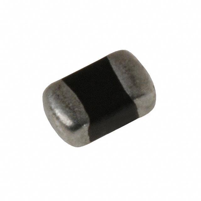
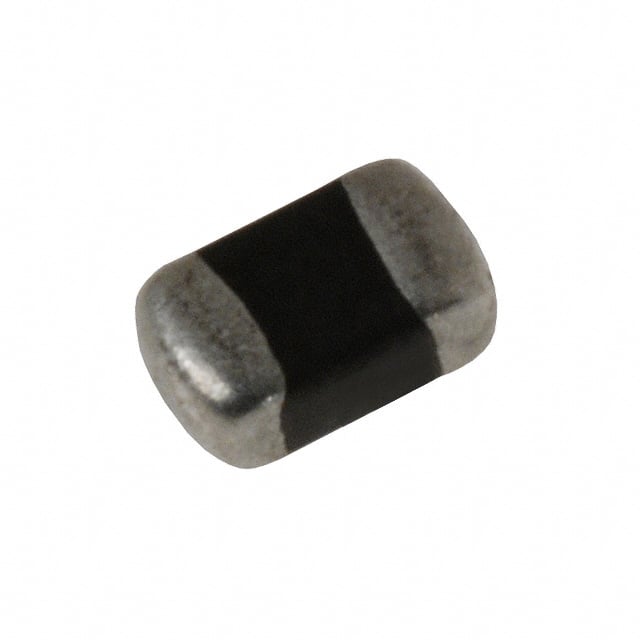
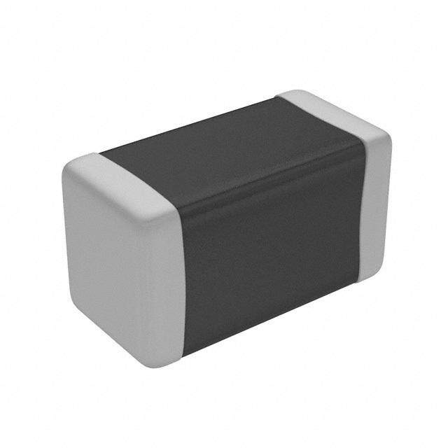
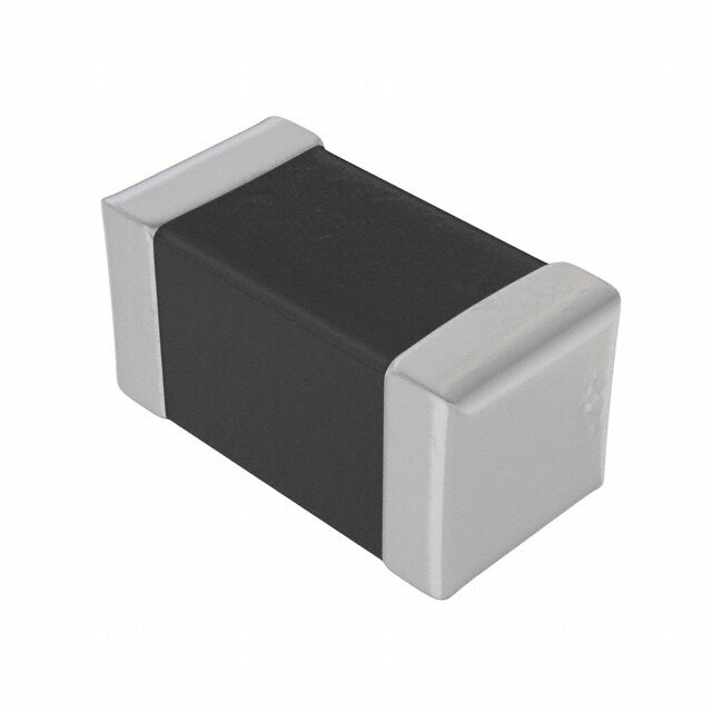
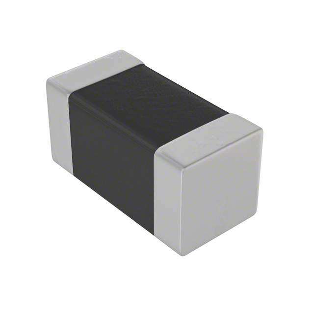
| 描述 | VARISTOR 22V 0805压敏电阻 18V |
| 产品分类 | |
| 品牌 | Littelfuse |
| 产品手册 | |
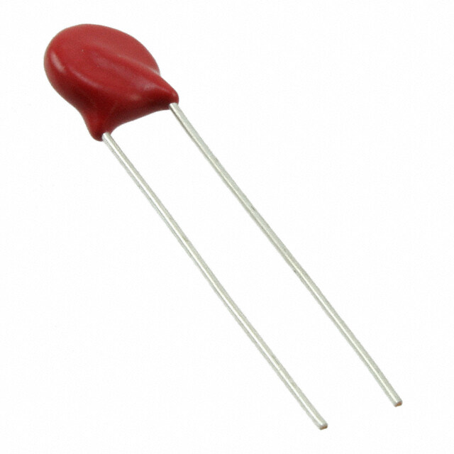
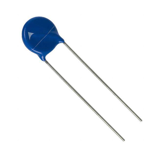
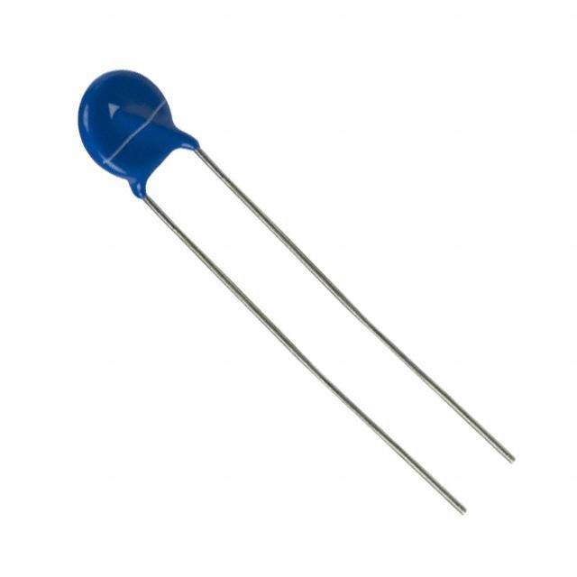
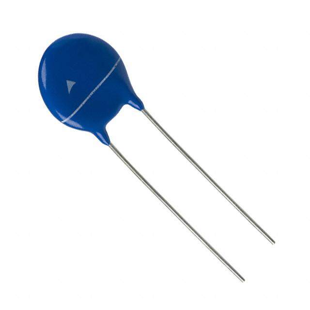
| 产品图片 |
|
| rohs | 符合RoHS不受无铅要求限制 / 符合限制有害物质指令(RoHS)规范要求 |
| 产品系列 | Littelfuse V18MLE0805HMLE |
| 数据手册 | |
| 产品型号 | V18MLE0805H |
| 产品 | MLV |
| 产品培训模块 | http://www.digikey.cn/PTM/IndividualPTM.page?site=cn&lang=zhs&ptm=25313 |
| 产品目录页面 | |
| 产品种类 | 压敏电阻 |
| 其它名称 | F2189DKR |
| 包装 | 剪切带 (CT) |
| 变阻器电压 | 22V |
| 商标 | Littelfuse |
| 外壳代码-in | 0805 |
| 外壳代码-mm | 2012 |
| 外壳宽度 | 1.25 mm |
| 安装 | SMD/SMT |
| 宽度 | 1.25 mm |
| 封装 | Reel |
| 封装/外壳 | 0805(2012 公制) |
| 封装/箱体 | 0805 (2012 metric) |
| 尺寸 | 1.25 mm W x 2.01 mm L x 1.1 mm H |
| 峰值浪涌电流 | 150 A |
| 工作温度范围 | - 55 C to + 125 C |
| 工厂包装数量 | 2500 |
| 最大AC电压 | - |
| 最大DC电压 | 18VDC |
| 标准包装 | 1 |
| 电压额定值DC | 18 V |
| 电容 | 100 pF |
| 电流-浪涌 | - |
| 电路数 | 1 |
| 端接类型 | SMD/SMT |
| 系列 | MLE |
| 能量 | - |
| 钳位电压 | 50 V |


- 商务部:美国ITC正式对集成电路等产品启动337调查
- 曝三星4nm工艺存在良率问题 高通将骁龙8 Gen1或转产台积电
- 太阳诱电将投资9.5亿元在常州建新厂生产MLCC 预计2023年完工
- 英特尔发布欧洲新工厂建设计划 深化IDM 2.0 战略
- 台积电先进制程称霸业界 有大客户加持明年业绩稳了
- 达到5530亿美元!SIA预计今年全球半导体销售额将创下新高
- 英特尔拟将自动驾驶子公司Mobileye上市 估值或超500亿美元
- 三星加码芯片和SET,合并消费电子和移动部门,撤换高东真等 CEO
- 三星电子宣布重大人事变动 还合并消费电子和移动部门
- 海关总署:前11个月进口集成电路产品价值2.52万亿元 增长14.8%

PDF Datasheet 数据手册内容提取
Metal-Oxide Varistors (MOVs) Surface Mount Multilayer Varistors (MLVs) > MLE Series MLE Varistor Series RoHS Description The MLE Series family of transient voltage suppression devices are based on the Littelfuse multilayer fabrication technology. These components are designed to suppress ESD events, including those specified in IEC 61000-4-2 or other standards used for Electromagnetic Compliance testing. The MLE Series is typically applied to protect integrated circuits and other components at the circuit board level operating at 18V , or less. DC The fabrication method and materials of these devices result in capacitance characteristics suitable for high frequency attenuation/low-pass filter circuit functions, Size Table thereby providing suppression and filtering in a single device. Metric EIA The MLE Series is manufactured from semiconducting 1005 0402 ceramics and is supplied in a leadless, surface mount package. The MLE Series is compatible with modern reflow 1608 0603 and wave soldering procedures. 2012 0805 Littelfuse Inc. manufactures other Multilayer Series 3216 1206 products. See the ML Series data sheet for higher energy/ peak current transient applications. See the AUML Series for automotive applications and the MLN Quad Array. For high–speed applications see the MHS Series. Applications Features • Protection of compliance (EMC) • Halogen-Free and operating temp. range components and RoHS Compliant • Used in mobile • Leadless 0402, 0603, circuits sensitive communications, • Rated for ESD 0805, and 1206 sizes to ESD Transients computer/EDP (IEC-61000-4-2) occurring on power • Operating voltages products, medical supplies, control products, hand held/ • Characterized for up to 18VM(DC) and signal lines portable devices, impedance and • Multilayer ceramic capacitance • Suppression of industrial equipment, construction technology ESD events such as including diagnostic • -55ºC to +125ºC specified in IEC-61000- port protection and 4-2 or MIL-STD-883 I/O interfaces Method-3015.7, for electromagnetic Additional Information Absolute Maximum Ratings • For ratings of individual members of a series, see device ratings and specifications table. Continuous MLE Series Units Steady State Applied Voltage: Datasheet Resources Samples DC Voltage Range (V ) ≤18 V M(DC) Operating Ambient Temperature -55 to +125 ºC Range (T ) A Storage Temperature Range (T ) -55 to +150 C STG © 2017 Littelfuse, Inc. Specifications are subject to change without notice. Revised: 09/14/17
Metal-Oxide Varistors (MOVs) Surface Mount Multilayer Varistors (MLVs) > MLE Series Device Ratings and Specifications Performance Specifications (25ºC) Max Continuous Working Voltage Nominal Maximum Clamping Maximum ESD Clamp -55ºC to 125ºC Voltage Voltage at Specified Voltage (Note 2) Typical Part Number Current (8/20µs) Capacitance (Note 1) V at 8kV Contact 15kV Air at 1MHz V 1mNOAM DC VC (Note 3) (Note 4) M(DC) (V) MIN (V) MAX (V) (V) (V) Clamp (V) (pF) V18MLE0402N 18 22 28 50 at 1A <125 <110 <55 V18MLE0402F (Note 8) 18 22 28 50 at 1A <125 <110 <55 V18MLE0603N 18 22 28 50 at 1A <75 <110 <125 V18MLE0603F (Note 8) 18 22 28 50 at 1A <75 <110 <125 V18MLE0603LN 18 22 28 50 at 1A <100 <140 <100 V18MLE0805N 18 22 28 50 at 1A <70 <75 <500 V18MLE0805LN 18 22 28 50 at 1A <75 <135 <290 V18MLE1206N 18 22 28 50 at 1A <65 <65 <1700 NOTES: 1. For applications of 18V or less. Higher voltages available, contact your Littelfuse Sales Representative. DC 2. Tested with IEC-61000-4-2 Human Body Model (HBM) discharge test circuit. 3. Direct discharge to device terminals (IEC preferred test method). 4. Corona discharge through air (represents actual ESD event). 5. Capacitance may be customized, contact your Littelfuse Sales Representative. 6. Leakage current ratings are at 18 V and 25µA maximum. DC 7. The typical capacitance rating is the discrete component test result. 8. Items are lead free, and available as "R" packing option only. Peak Current and Energy Derating Curve Nominal Voltage Stability to Multiple ESD Impulses (8kV Contact Discharges per IEC 61000-4-2) For applications exceeding 125ºC ambient temperature, the peak surge current and energy ratings must be reduced as shown below. 30 DC 25 A 100 m NT OF RATED VALUE 864000 OMINAL VOLTAGE AT 1 2115050 E N C PER 20 0 1 10 100 1000 10000 0 Figure 2 CURRENT (A) -55 50 60 70 80 90 100 110 120 130 140 150 FIGURE 2. NOMINAL VOLTAGE STABILITY TO MULTIPLE Figure 1 AMBIENT TEMPERATURE (oC) ESD IMPULSES (8KV CONTACT DISCHARGES FIGURE 1. PEAK CURRENT AND ENERGY DERATING CURVE PER IEC 61000-4-2) Standby Current at Normalized Varistor Voltage and Temperature Impedance (Z) vs Frequency Typical Characteristic 1.2 100 V) GE ( 1.0 -0402 LTA 10 -0603 O OR V 0.8 -0805 D VARIST 0.6 2855OO NCE (Z) 1 -1206 E A Z 0.4 D ORMALI 0.2 125O IMPE 0.1 N 0.0 0.01 0.0001 0.001 0.01 0.1 1 10 100 1000 10000 Figure 3 CURRENT (mA) Figure 4 FREQUENCY (MHz) FIGURE 3. STANDBY CURRENT AT NORMALIZED VARISTOR FIGURE 4. IMPEDANCE (Z) vs FREQUENCY VOLTAGE AND TEMPERATURE TYPICAL CHARACTERISTIC © 2017 Littelfuse, Inc. Specifications are subject to change without notice. Revised: 09/14/17
Metal-Oxide Varistors (MOVs) Surface Mount Multilayer Varistors (MLVs) > MLE Series Device Characteristics Clamping Voltage Over Temperature (V at 10A) C At low current levels, the V-I curve of the multilayer 100 transient voltage suppressor approaches a linear (ohmic) relationship and shows a temperature dependent effect. At or below the maximum working voltage, the suppressor E (V) V26MLA1206 is in a high resistance model (approaching 106Ω at its G A maximum rated working voltage). Leakage currents at LT O V maximum rated voltage are below 100µA, typically 25µA; G N for 0402 size below 20µA, typically 5µA. PI M A L C Typical Temperature Dependance of the Characteristic V5.5MLA1206 Curve in the Leakage Region 100% GE IN PERCENT OFoAT 25C (%) FigureF1 I0G6-6U0RE- 4102. (CV-L2CA0 AMTP 1I0N0AGT) EVM2O0PLETRAAG4T0EU ROE6V (0EoCR) T8E0MP1E0R0ATU12R0E140 RESSOR VOLTA VALUE VNOM EEnneerrggyy dAisbssiopraptetido nw/iPtheina kt hCeu MrreLnEt i sC acaplacbulialitteyd by P P SU 25o 50o 75o 100o 125oC multiplying the clamping voltage, transient current 10% 1E-9 1E-8 1E-7 1E-6 1E-5 1E-4 1E-3 1E-2 and transient duration. An important advantage of the Figure 5 SUPPRESSOR CURRENT (ADC) multilayer is its interdigitated electrode construction within FIGURE 10. TYPICAL TEMPERATURE DEPENDANCE OF THE CHARACTERISTIC the mass of dielectric material. This results in excellent CURVE IN THE LEAKAGE REGION current distribution and the peak temperature per energy Speed of Response absorbed is very low. The matrix of semiconducting grains combine to absorb and distribute transient energy (heat) The Multilayer Suppressor is a leadless device. Its (see Speed of Response). This dramatically reduces peak response time is not limited by the parasitic lead temperature; thermal stresses and enhances device inductances found in other surface mount packages. reliability. The response time of the Z O dielectric material is less N than 1ns and the MLE can clamp very fast dV/dT events As a measure of the device capability in energy and peak such as ESD. Additionally, in "real world" applications, current handling, the V26MLA1206A part was tested with the associated circuit wiring is often the greatest multiple pulses at its peak current rating (3A, 8/20µs). At factor effecting speed of response. Therefore, transient the end of the test, 10,000 pulses later, the device voltage suppressor placement within a circuit can be considered characteristics are still well within specification. important in certain instances. Repetitive Pulse Capability Multilayer Internal Construction 100 PEAK CURRENT = 3A FIRED CERAMIC 8/20s DURATION, 30s BETWEEN PULSES DIELECTRIC E V26MLA1206 G A LT O METAL V ELECTRODES METAL END TERMINATION DEPLETION 10 REGION 0 2000 4000 6000 8000 10000 12000 DEPLETION Figure 8 NUMBER OF PULSES REGION FIGURE 13. REPETITIVE PULSE CAPABILITY Figure 7 GRAINS FIGURE 11. MULTILAYER INTERNAL CONSTRUCTION © 2017 Littelfuse, Inc. Specifications are subject to change without notice. Revised: 09/14/17
Metal-Oxide Varistors (MOVs) Surface Mount Multilayer Varistors (MLVs) > MLE Series Lead (Pb) Soldering Recommendations The principal techniques used for the soldering of Reflow Solder Profile components in surface mount technology are IR Re-flow and Wave soldering. Typical profiles are shown on the right. The recommended solder for the MLE suppressor is 230 a 62/36/2 (Sn/Pb/Ag), 60/40 (Sn/Pb) or 63/37 (Sn/Pb). Littelfuse also recommends an RMA solder flux. 230 Wave soldering is the most strenuous of the processes. To avoid the possibility of generating stresses due to thermal shock, a preheat stage in the soldering process is recommended, and the peak temperature of the solder 230 process should be rigidly controlled. When using a reflow process, care should be taken to ensure that the MLE chip is not subjected to a thermal Figure 9 gradient steeper than 4 degrees per second; the ideal 5. gradient being 2 degrees per second. During the soldering Wave Solder Profile process, preheating to within 100 degrees of the solder's 5. peak temperature is essential to minimize thermal shock. Once the soldering process has been completed, it is still necessary to ensure that any further thermal shocks are avoided. One possible cause of thermal shock is hot 5. printed circuit boards being removed from the solder process and subjected to cleaning solvents at room temperature. The boards must be allowed to cool gradually to less than 50ºC before cleaning. 6. Figure 10 6. MAXIMUM TEMPERATURE 260˚C Lead–free (Pb-free) Soldering Recommendations 20 - 40 SECONDS WITHIN 5˚C MAXIMUM TEMPREARMAPT URRAETE 260˚C Littelfuse offers the Nickel Barrier Termination finish for the 20 - 40 SECOND<S3 ˚WCI/TsHIN 5˚C 60 - 150 SEC Lead–free Re-flow Pr6o.file > 217˚C optimum Lead–free solder performance. RAMP RATE <3˚C/s 60 - 150 SEC > 217˚C The preferred solder is 96.5/3.0/0.5 (SnAgCu) with an RMA PREHEAT ZONE flux, but there is a wide selection of pastes and fluxes MAXIMUM TEMPERATURE 260˚C available with which the Nickel Barrier parts should be 20 - 40 SECONDS WITHIN 5˚C PREHEAT ZONE compatible. RAMP RATE <3˚C/s 56.00 - 1 5 0 S6.E0C 7.0 > 217˚C The reflow profile must be constrained by the maximums in the Lead–free Reflow Profile. For Lead–free Wave FIGURE 7. LEAD-FREE RE-FLOW 5P.R0 O F I L E 6.0 7.0 soldering, the Wave Solder Profile still applies. PREHEAT ZONE FIGURE 7. LEAD-FREE RE-FLOW PROFILE Note: the Lead–free paste, flux and profile were used for evaluation purposes by Littelfuse, based upon industry standards and practices. There are multiple choices of all 5.0 6.0 7.0 Figure 11 three available, it is advised that the customer explores the optimum combination for their process as processes vary FIGURE 7. LEAD-FREE RE-FLOW PROFILE considerably from site to site. © 2017 Littelfuse, Inc. Specifications are subject to change without notice. Revised: 09/14/17
Metal-Oxide Varistors (MOVs) Surface Mount Multilayer Varistors (MLVs) > MLE Series Product Dimensions (mm) PAD LAYOUT DEMENSIONS CHIP LAYOUT DIMENSIONS C E B NOTE D L A W NOTE: Avoid metal runs in this area. NotNeo: tAev: oAidvo mide mtael traul nrusn ins itnh itsh iasr earae,a p, apratrst sa arere n ot recnoomt mreecnodmemd efonrd euds ef oinr uaspep ilnic aaptipolnicsa tuiosninsg u ssiilnvge r (AgS)i levxepr o(Axgy ) peapsotxey. paste. 1206 Size 0805 Size 0603 Size 0402 Size Dimension IN MM IN MM IN MM IN MM A 0.160 4.06 0.120 3.05 0.100 2.54 0.067 1.70 B 0.065 1.65 0.050 1.27 0.030 0.76 0.020 0.51 C 0.040 1.02 0.040 1.02 0.035 0.89 0.024 0.61 D (max.) 0.071 1.80 0.043 1.10 0.040 1.00 0.024 0.60 0.015 -/+ 0.010 -/+ E 0.02 -/+ 0.01 0.50 -/+ 0.25 0.02 -/+ 0.01 0.50 -/+ 0.25 0.4 -/+ 0.2 0.25 -/+ 0.15 0.008 0.006 0.125 -/+ 0.079 -/+ 0.063 -/+ 0.039 -/+ L 3.20 -/+ 0.03 2.01 -/+ 0.2 1.6 -/+ 0.15 1.0 -/+ 0.1 0.012 0.008 0.006 0.004 0.049 -/+ 0.032 -/+ 0.020 -/+ W 0.06 -/+ 0.011 1.60 -/+ 0.28 1.25 -/+ 0.2 0.8 -/+ 0.15 0.5 -/+ 0.1 0.008 0.006 0.004 Part Numbering System V 18 MLE1206 X X X DEVICE FAMILY PACKING OPTIONS (see Packaging section for quantities) Littelfuse TVSS Device T: 13in (330mm) Diameter Reel, Plastic Carrier Tape H: 7in (178mm) Diameter Reel, Plastic Carrier Tape MAXIMUM DC R: 7in (178mm) Diameter Reel, Paper Carrier Tape WORKING VOLTAGE END TERMINATION OPTION MULTILAYER SERIES N: Nickel Barrier( Ni/Sn) DESIGNATOR F: Lead free with Nickel Barrier(Ni/Sn) DEVICE SIZE: i.e., 120 mil x 60 mil CAPACITANCE OPTION (3mm x 1.5mm) No Letter:Standard L:Low Capacitance Version Packaging* Quantity Device Size 13” Inch Reel 7” Inch Reel 7” Inch Reel Bulk Pack ('T' Option) ('H' Option) ('R' Option) ('A' Option) 1206 10,000 2,500 N/A 2500 0805 10,000 2,500 N/A 2500 0603 10,000 2,500 4,000 2500 0402 N/A N/A 10,000 N/A *(Packaging) It is recommended that parts be kept in the sealed bag provided and that parts be used as soon as possible when removed from bags. © 2017 Littelfuse, Inc. Specifications are subject to change without notice. Revised: 09/14/17
Metal-Oxide Varistors (MOVs) Surface Mount Multilayer Varistors (MLVs) > MLE Series Tape and Reel Specifications PRODUCT D0 P0 IDENTIFYING For T and H Pack Options: PLASTIC CARRIER TAPE LABEL P2 For R Pack Options: EMBOSSED PAPER CARRIER TAPE E F W K0 B0 EMBOSSMENT t1 D1 P1 A0 TOP TAPE NO8MmINmAL O1R7 383m0mmm DIA. REEL Dimensions in Millimeters Symbol Description 0402 Size 0603, 0805 & 1206 Sizes A Width of Cavity Dependent on Chip Size to Minimize Rotation. 0 B Length of Cavity Dependent on Chip Size to Minimize Rotation. 0 K Depth of Cavity Dependent on Chip Size to Minimize Rotation. 0 W Width of Tape 8 -/+ 0.2 8 -/+ 0.3 F Distance Between Drive Hole Centers and Cavity Centers 3.5 -/+ 0.05 3.5 -/+ 0.05 E Distance Between Drive Hole Centers and Tape Edge 1.75 -/+ 0.1 1.75 -/+ 0.1 P Distance Between Cavity Centers 2 -/+ 0.05 4 -/+ 0.1 1 P Axial Drive Distance Between Drive Hole Centers & Cavity Centers 2 -/+ 0.1 2 -/+ 0.1 2 P Axial Drive Distance Between Drive Hole Centers 4 -/+ 0.1 4 -/+ 0.1 0 D Drive Hole Diameter 1.55 -/+ 0.05 1.55 -/+ 0.05 0 D Diameter of Cavity Piercing N/A 1.05 -/+ 0.05 1 T Top Tape Thickness 0.1 Max 0.1 Max 1 Notes : • Conforms to EIA-481-1, Revision A • Can be supplied to IEC publication 286-3 Disclaimer Notice - Information furnished is believed to be accurate and reliable. However, users should independently evaluate the suitability of and test each product selected for their own applications. Littelfuse products are not designed for, and may not be used in, all applications. Read complete Disclaimer Notice at www.littelfuse.com/disclaimer-electronics. © 2017 Littelfuse, Inc. Specifications are subject to change without notice. Revised: 09/14/17