 Datasheet下载
- 型号: V150C28C150BL
- 制造商: Vicor
- 库位|库存: xxxx|xxxx
- 要求:
| 数量阶梯 | 香港交货 | 国内含税 |
| +xxxx | $xxxx | ¥xxxx |
查看当月历史价格
查看今年历史价格
V150C28C150BL产品简介:
ICGOO电子元器件商城为您提供V150C28C150BL由Vicor设计生产,在icgoo商城现货销售,并且可以通过原厂、代理商等渠道进行代购。 V150C28C150BL价格参考。VicorV150C28C150BL封装/规格:直流转换器, 隔离模块 DC/DC 转换器 1 输出 28V 5.36A 100V - 200V 输入。您可以下载V150C28C150BL参考资料、Datasheet数据手册功能说明书,资料中有V150C28C150BL 详细功能的应用电路图电压和使用方法及教程。
Vicor Corporation的V150C28C150BL是一款高性能的直流-直流转换器模块,广泛应用于需要高效、高密度电源解决方案的场合。该模块具有宽输入电压范围、高转换效率和紧凑的封装设计,适用于以下主要应用场景:

1. 工业自动化设备:用于为PLC、工业计算机、传感器和执行器等提供稳定可靠的电源。

2. 通信设备:广泛应用于基站、路由器、交换机等通信基础设施中,为系统提供高效、稳定的直流电源。

3. 测试与测量仪器:用于高精度测试设备中,确保设备在复杂环境下仍能稳定运行。

4. 航空航天与国防系统:由于其高可靠性和优异的热管理性能,适用于对电源要求严苛的航空航天和军事设备。

5. 医疗电子设备:用于诊断设备、监护仪等精密医疗仪器中,提供安全、稳定的电力支持。

6. 嵌入式系统与服务器电源:适用于高密度计算系统和数据中心服务器的电源架构中,提高整体能效。

该模块支持高输入电压(150V),输出为28V/150A,具备良好的动态响应和过载保护功能,适用于需要高功率密度和高可靠性的电源系统设计。
| 参数 | 数值 |
| 产品目录 | |
| 描述 | CONVERTER MOD DC/DC 28V 150W |
| 产品分类 | DC DC Converters |
| 品牌 | Vicor Corporation |
| 数据手册 | |
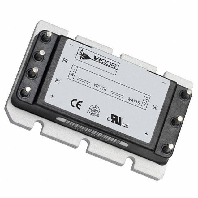
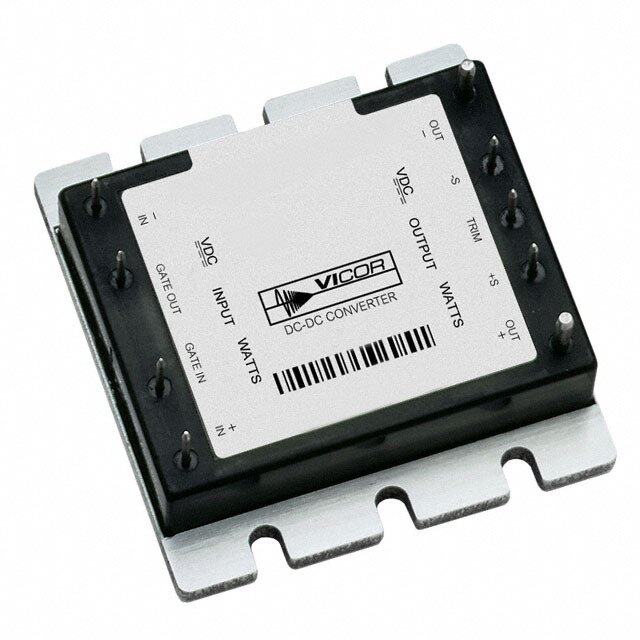
| 产品图片 |
|
| 产品型号 | V150C28C150BL |
| rohs | 含铅 / 不符合限制有害物质指令(RoHS)规范要求 |
| 产品系列 | 微型 |
| 其它名称 | 1102-1242 |
| 功率(W)-制造系列 | 150W |
| 功率(W)-最大值 | 150W |
| 包装 | 散装 |
| 大小/尺寸 | 2.28" 长 x 1.45" 宽 x 0.65" 高(57.9mm x 36.8mm x 16.5mm) |
| 安装类型 | 通孔 |
| 封装/外壳 | 四分之一砖 |
| 工作温度 | -20°C ~ 100°C |
| 效率 | 87.5% |
| 标准包装 | 1 |
| 特性 | OVP,UVLO |
| 电压-输入(最大值) | 200V |
| 电压-输入(最小值) | 100V |
| 电压-输出1 | 28V |
| 电压-输出2 | - |
| 电压-输出3 | - |
| 电压-隔离 | 3kV(3000V) |
| 电流-输出(最大值) | 5.36A |
| 相关产品 | /product-detail/zh/ATS-1141-C1-R0/ATS1500-ND/4146482/product-detail/zh/ATS-1139-C1-R0/ATS1499-ND/4146481/product-detail/zh/ATS-1138-C1-R0/ATS1498-ND/4146480/product-detail/zh/ATS-1099-C1-R0/ATS1496-ND/4146479/product-detail/zh/ATS-1098-C1-R0/ATS1495-ND/4146478/product-detail/zh/ATS-1101-C1-R0/ATS1497-ND/4146471 |
| 类型 | 隔离模块 |
| 设计资源 | |
| 输出数 | 1 |


PDF Datasheet 数据手册内容提取
Micro Family 150V Input Actual size: 2.28 x 1.45 x 0.5in ® S 57,9 x 36,8 x 12,7mm C US C NRTL US DC-DC Converter Module Features & Benefits Applications • DC input range: 100 – 200V Communications, control systems, medical, instrumentation, defense and aerospace. • Isolated output For details on proper operation please refer to the: • Encapsulated circuitry for shock and Design Guide & Applications Manual for Maxi, Mini, Micro Family. vibration resistance • Extended temperature range (–55 to +100°C) Absolute Maximum Ratings • Input surge withstand: 250V for 100ms • DC output: 3.3 – 48V Parameter Rating Unit Notes • Programmable output: 10 to 110% +IN to -IN voltage -0.5 to +260 V • Regulation: ±0.2% no load to full load DC PC to -IN voltage -0.5 to +7.0 V • Efficiency: Up to 88% DC PR to -IN voltage -0.5 to +7.0 V • Maximum operating temp: 100°C, DC full load SC to -OUT voltage -0.5 to +1.5 VDC • Power density: up to 91W per cubic inch Isolation voltage IN to OUT 3000 V Test voltage • Height above board: 0.43in. (10,9mm) RMS IN to base 1500 V Test voltage • Parallelable, with N+M fault tolerance RMS OUT to base 500 V Test voltage • Low noise ZCS/ZVS architecture RMS Operating Temperature -55 to +100 °C M-Grade • RoHS Compliant (with F or G pin option) Storage Temperature -65 to +125 °C M-Grade 500 (260) °F (°C) <5 sec; wave solder Product Overview Pin soldering temperature 750 (390) °F (°C) <7 sec; hand solder These DC-DC converter modules use Mounting torque 5 (0.57) in-lbs (N-m) 6 each advanced power processing, control and packaging technologies to provide the performance, flexibility, reliability and cost effectiveness of a mature power component. High frequency ZCS/ZVS switching provides high power density with low noise and high efficiency. Part Numbering V150C B e.g. V150C12C150BL Output Voltage Product Grade Temperatures (°C) Output Power Pin Style Finish Baseplate 3V583 === 358.VV3 V G rCEa d e == --O1200p ettrooa t++in11g00 00 --24S00t ottoora ++ge112255 35V.VO3U VT P71O50UW0TW LSB::l aLSnohnkog:r tS hMoortd uMate TTiinnG//oLLeeldaa dd B23::l aTTnhhkrreo: auSdgloehtd-the do le 12 = 12V T = -40 to +100 -40 to +125 8V 100W N: Long ModuMate Gold 15 = 15V H = -40 to +100 -55 to +125 12V 150W F: Short RoHS Gold 24 = 24V M = -55 to +100 -65 to +125 15V 150W G: Long RoHS Gold 28 = 28V 24V 150W K: Extra Long RoHS Gold 36 = 36V 28V 150W 48 = 48V 36V 150W 48V 150W 150V Micro Family Rev 3.1 vicorpower.com Page 1 of 11 06/2017 800 927.9474
150V Input Module Family Electrical Characteristics Electrical characteristics apply over the full operating range of input voltage, output load (resistive) and baseplate temperature, unless otherwise specified. All temperatures refer to the operating temperature at the center of the baseplate. MODULE INPUT SPECIFICATIONS Parameter Min Typ Max Unit Notes Operating input voltage 100 150 200 V DC Input surge withstand 250 V <100ms DC Undervoltage turn-on 97.0 99.0 V DC Undervoltage turn-off 81.9 84.9 V DC Overvoltage turn-off/on 201.9 210 220 V DC Disabled input current 1.1 mA PC pin low MODULE OUTPUT SPECIFICATIONS Parameter Min Typ Max Unit Notes Output voltage setpoint ±1 % Of nominal output voltage. Nominal input; full load; 25°C Line regulation ±0.02 ±0.20 % Low line to high line; full load Temperature regulation ±0.002 ±0.005 % / °C Over operating temperature range Power sharing accuracy ±2 ±5 % 10 to 100% of full load Of nominal output voltage. For trimming below 90% Programming range 10 110 % of nominal, a minimum load of 10% of maximum rated power may be required. +OUT to –OUT — Absolute Maximum Ratings 3.3V –0.5 to 4.7 V Externally applied DC 5V –0.5 to 7.0 V Externally applied DC 8V –0.5 to 10.9 V Externally applied DC 12V –0.5 to 16.1 V Externally applied DC 15V –0.5 to 20.0 V Externally applied DC 24V –0.5 to 31.7 V Externally applied DC 28V –0.5 to 36.9 V Externally applied DC 36V –0.5 to 47.4 V Externally applied DC 48V –0.5 to 62.9 V Externally applied DC Note: The permissible load current must never be exceeded during normal, abnormal or test conditions. For additional output related application information, please refer to output connections on page 6. THERMAL RESISTANCE AND CAPACITY Parameter Min Typ Max Unit Baseplate to sink; flat, greased surface 0.24 °C/Watt Baseplate to sink; thermal pad (P/N 20265) 0.21 °C/Watt Baseplate to ambient 10.9 °C/Watt Baseplate to ambient; 1000LFM 2.8 °C/Watt Thermal capacity 48 Watt-sec/°C 150V Micro Family Rev 3.1 vicorpower.com Page 2 of 11 06/2017 800 927.9474
150V Input Module Family Electrical Characteristics (Cont.) MODULE CONTROL SPECIFICATIONS Parameter Min Typ Max Unit Notes Primary Side (PC = Primary Control; PR = Parallel) PC bias voltage 5.50 5.75 6.00 V PC current = 1.0mA DC current limit 1.5 2.1 3.0 mA PC voltage = 5.5V PC module disable 2.3 2.6 2.9 VDC Switch must be able to sink ≥4 mA. See Fig. 2 PC module enable delay 4 7 ms PC module alarm 0.5 Vavg UV, OV, OT, module fault. See Figs. 3 and 5 PC resistance 0.9 1.0 1.1 MΩ See Fig. 3, converter off or fault mode PR emitter amplitude 5.7 5.9 6.1 Volts PR load >30Ω, <30pF PR emitter current 150 mA PR receiver impedance 375 500 625 Ω 25°C PR receiver threshold 2.4 2.5 2.6 Volts Minimum pulse width: 20ns PR drive capability 12 modules Without PR buffer amplifier Secondary Side (SC = Secondary Control) SC bandgap voltage 1.21 1.23 1.25 V Referenced to –Sense DC SC resistance 990 1000 1010 Ω SC capacitance 0.033 µF SC module alarm 0 V With open trim; referenced to –Sense. See Fig. 7 DC MODULE GENERAL SPECIFICATIONS Parameter Min Typ Max Unit Notes Isolation test voltage (IN to OUT)* 3000 V Complies with reinforced insulation requirements RMS Isolation test voltage (IN to base)* 1500 V Complies with basic insulation requirements RMS Isolation test voltage (OUT to base)* 500 V Complies with operational insulation requirements RMS Isolation resistance 10 MΩ IN to OUT, IN to baseplate, OUT to baseplate 1.9 2.1 2.3 ounces Weight (E, C, T grade) (52.8) (59.3) (65.8) (grams) 2.1 2.3 2.5 ounces Weight (H, M grade) (58.7) (65.2) (71.7) (grams) Temperature limiting 100 115 °C See Figs. 3 and 5. Do not operate coverter >100°C. UL60950-1, EN60950-1, CSA60950-1, IEC60950-1. Agency approvals cURus, cTÜVus, CE With appropriate fuse in series with the +Input * Isolation test voltage, 1 minute or less. Note: Specifications are subject to change without notice. 150V Micro Family Rev 3.1 vicorpower.com Page 3 of 11 06/2017 800 927.9474
150V Input MODULE SPECIFIC OPERATING SPECIFICATIONS 3.3V , 75W (e.g. V150C3V3C75BL) OUT Parameter Min Typ Max Unit Notes Efficiency 78 79 % Nominal input; full load; 25°C Ripple and noise 94 118 mV p-p; Nominal input; full load; 20MHz bandwidth Output OVP setpoint 4.14 4.3 4.46 Volts 25°C; recycle input voltage or PC to restart (>100ms off) Dissipation, standby 3.3 3.9 Watts No load Load regulation ±0.02 ±0.2 % No load to full load; nominal input Load current 0 22.7 Amps Current limit 23.1 26.1 30.7 Amps Output voltage 95% of nominal Short circuit current 15.8 26.1 30.7 Amps Output voltage <250mV 5V , 100W (e.g. V150C5C100BL) OUT Parameter Min Typ Max Unit Notes Efficiency 81.5 82.7 % Nominal input; full load; 25°C Ripple and noise 180 225 mV p-p; Nominal input; full load; 20MHz bandwidth Output OVP setpoint 6.03 6.25 6.47 Volts 25°C; recycle input voltage or PC to restart (>100ms off) Dissipation, standby 4.5 6.7 Watts No load Load regulation ±0.02 ±0.2 % No load to full load; nominal input Load current 0 20 Amps Current limit 20.4 23 27 Amps Output voltage 95% of nominal Short circuit current 14 23 27 Amps Output voltage <250mV 8V , 100W (e.g. V150C8C100BL) OUT Parameter Min Typ Max Unit Notes Efficiency 82.5 84 % Nominal input; full load; 25°C Ripple and noise 180 215 mV p-p; Nominal input; full load; 20MHz bandwidth Output OVP setpoint 9.36 9.7 10.1 Volts 25°C; recycle input voltage or PC to restart (>100ms off) Dissipation, standby 5.3 7.5 Watts No load Load regulation ±0.02 ±0.2 % No load to full load; nominal input Output Current 0 12.5 Amps Current limit 12.7 14.4 16.9 Amps Output voltage 95% of nominal Short circuit current 8.75 14.4 16.9 Amps Output voltage <250mV 12V , 150W (e.g. V150C12C150BL) OUT Parameter Min Typ Max Unit Notes Efficiency 86.5 87.5 % Nominal input; full load; 25°C Ripple and noise 220 275 mV p-p; Nominal input; full load; 20MHz bandwidth Output OVP setpoint 13.7 14.3 14.9 Volts 25°C; recycle input voltage or PC to restart (>100ms off) Dissipation, standby 5.5 11 Watts No load Load regulation ±0.02 ±0.2 % No load to full load; nominal input Load current 0 12.5 Amps Current limit 12.7 14.4 16.9 Amps Output voltage 95% of nominal Short circuit current 8.75 14.4 16.9 Amps Output voltage <250mV 15V , 150W (e.g. V150C15C150BL) OUT Parameter Min Typ Max Unit Notes Efficiency 86.9 87.9 % Nominal input; full load; 25°C Ripple and noise 135 169 mV p-p; Nominal input; full load; 20MHz bandwidth Output OVP setpoint 17.1 17.8 18.5 Volts 25°C; recycle input voltage or PC to restart (>100ms off) Dissipation, standby 3.6 4.8 Watts No load Load regulation ±0.02 ±0.2 % No load to full load; nominal input Load current 0 10 Amps Current limit 10.2 11.5 13.5 Amps Output voltage 95% of nominal Short circuit current 7 11.5 13.5 Amps Output voltage <250mV 150V Micro Family Rev 3.1 vicorpower.com Page 4 of 11 06/2017 800 927.9474
150V Input MODULE SPECIFIC OPERATING SPECIFICATIONS (CONT.) 24V , 150W (e.g. V150C24C150BL) OUT Parameter Min Typ Max Unit Notes Efficiency 86 87.7 % Nominal input; full load; 25°C Ripple and noise 64 80 mV p-p; Nominal input; full load; 20MHz bandwidth Output OVP setpoint 27.1 28.1 29.1 Volts 25°C; recycle input voltage or PC to restart (>100ms off) Dissipation, standby 4.3 5 Watts No load Load regulation ±0.02 ±0.2 % No load to full load; nominal input Load current 0 6.25 Amps Current limit 6.37 7.19 8.44 Amps Output voltage 95% of nominal Short circuit current 4.37 7.19 8.44 Amps Output voltage <250mV 28V , 150W (e.g. V150C28C150BL) OUT Parameter Min Typ Max Unit Notes Efficiency 86.9 87.5 % Nominal input; full load; 25°C Ripple and noise 80 100 mV p-p; Nominal input; full load; 20MHz bandwidth Output OVP setpoint 31.5 32.7 33.9 Volts 25°C; recycle input voltage or PC to restart (>100ms off) Dissipation, standby 5.3 7.4 Watts No load Load regulation ±0.02 ±0.2 % No load to full load; nominal input Output Current 0 5.36 Amps Current limit 5.46 6.16 7.24 Amps Output voltage 95% of nominal Short circuit current 3.75 6.16 7.24 Amps Output voltage <250mV 36V , 150W (e.g. V150C36C150BL) OUT Parameter Min Typ Max Unit Notes Efficiency 82.9 84.6 % Nominal input; full load; 25°C Ripple and noise 69 87 mV p-p; Nominal input; full load; 20MHz bandwidth Output OVP setpoint 40.4 41.9 43.4 Volts 25°C; recycle input voltage or PC to restart (>100ms off) Dissipation, standby 5.4 6.3 Watts No load Load regulation ±0.02 ±0.2 % No load to full load; nominal input Output Current 0 4.17 Amps Current limit 4.25 4.8 5.63 Amps Output voltage 95% of nominal Short circuit current 2.91 4.8 5.63 Amps Output voltage <250mV 48V , 150W (e.g. V150C48C150BL) OUT Parameter Min Typ Max Unit Notes Efficiency 86.9 88.1 % Nominal input; full load; 25°C Ripple and noise 80 100 mV p-p; Nominal input; full load; 20MHz bandwidth Output OVP setpoint 53.7 55.7 57.7 Volts 25°C; recycle input voltage or PC to restart (>100ms off) Dissipation, standby 5.8 6.7 Watts No load Load regulation ±0.02 ±0.2 % No load to full load; nominal input Load current 0 3.13 Amps Current limit 3.19 3.6 4.23 Amps Output voltage 95% of nominal Short circuit current 2.19 3.6 4.23 Amps Output voltage <250mV 150V Micro Family Rev 3.1 vicorpower.com Page 5 of 11 06/2017 800 927.9474
150V Input Basic Module Operation C2* C4* 4.7nF 4.7nF +IN +OUT F1* PC C1* SC 0.2µF PR –IN –OUT C3* C5* 4.7nF 4.7nF For C1 – C5, keep leads and connections short. Figure 1 — Basic module operation requires fusing, grounding, bypassing capacitors.* See Maxi, Mini, Micro Design Guide. Output Connections and Considerations leads must be protected for conditions such as lead reversal, noise pickup, open circuit, or excessive output lead resistance The permissible load current must never be exceeded during between the sense point and the converters output terminals. normal, abnormal or test conditions. Converters subject to For applications that may draw more than the rated current, a dynamic loading exceeding 25% of rated current must be fast acting electronic circuit breaker must be utilized to protect reviewed by Vicor Applications Engineering to ensure that the the converter. Under no circumstance should the rated current converter will operate properly. be exceeded. Utilizing or testing of current limit or short circuit Under dynamic load, light load, or no load conditions, the current will damage the converter. Ensure that the total output converter may emit audible noise. Converters that utilize remote capacitance connected to the converter does not exceed sense may require compensation circuitry to offset the phase the limits on Page 16, “Maximum Output Capacitance”, of lag caused by the external output leads and load impedance. the design guide. If an external remote sense circuit is used, the remote sense Comprehensive Online Application Information The Design Guide and Applications Manual includes: • Application circuits • Design requirements • EMC considerations • Current sharing in power arrays • Thermal performance information • Recommended soldering methods • Accessory modules – filtering, rectification, front-ends • Mounting options • ...and more. CLICK HERE TO VIEW DESIGN GUIDE Also at vicorpower.com • PowerBench online configurators • Over 20 Application Notes • Online calculators – thermal, trimming, hold-up • PDF data sheets for ALL Vicor products 150V Micro Family Rev 3.1 vicorpower.com Page 6 of 11 06/2017 800 927.9474
150V Input Primary Control - PC PIN Module Enable/Disable Module Alarm The module may be disabled by pulling PC to 0V (2.3V max) The module contains “watchdog” circuitry which monitors with respect to the –Input. This may be done with an open input voltage, operating temperature and internal operating collector transistor, relay, or optocoupler. Converters may be parameters. In the event that any of these parameters are disabled with a single transistor or relay either directly or via outside of their allowable operating range, the module will shut “OR’ing” diodes for 2 or more converters. See Figure 2. down and PC will go low. PC will periodically go high and the module will check to see if the fault (as an example, Primary Auxiliary Supply Input Undervoltage) has cleared. If the fault has not been cleared, PC will go low again and the cycle will restart. The SC During normal operation only, the PC Pin can source 5.7V pin will go low in the event of a fault and return to its normal @ 1.5mA. In the example shown in Figure 4, PC powers a state after the fault has been cleared. See Figures 3 and 5. module enabled LED. Input Undervoltage Input Overvoltage [a] +IN Over Temperature +OUT Module Faults +IN +OUT Auto Restart SW1 PC 50Ω PC 2-2f0(mVIsN )typ. 1K SC SC PR SW2 SW3 PR 1M (05-.73VmDAC) 6K Disable 1.23 –IN SW1, 2, & 3 shown VDC –OUT –IN –OUT in "Fault" position Disable = PC < 2.3V [a] Not applicable for 300V Input family DC Figure 2 — Module enable/disable Figure 3 — PC/SC module alarm logic +IN +OUT Fault 40µs typ. 5.7V PC PC 4kΩ SC "Module PR Enabled" –IN –OUT SC 1.23V 2-20ms typ. Figure 4 — LED on-state indicator Figure 5 —PC/SC module alarm timing Optocoupler +IN +IN +OUT +OUT Comparator PC PC SC SC 4k PR PR Alarm 1.00V –IN –IN –OUT –OUT Figure 6 —Isolated on-state indicator Figure 7 — Secondary side on-state indicator 150V Micro Family Rev 3.1 vicorpower.com Page 7 of 11 06/2017 800 927.9474
150V Input Secondary Control - SC PIN Compatible interface architectures include the following: AC coupled single-wire interface. All PR pins are connected Output Voltage Programming to a single communication bus through 0.001µF (500V) The output voltage of the converter can be adjusted or capacitors. This interface supports current sharing and is fault programmed via fixed resistors, potentiometers or voltage tolerant except for the communication bus. Up to three DACs. See Figure 8. converters may be paralleled by this method. See Figure 9. Transformer coupled interface. For paralleling four or more converters a transformer coupled interface is required, and under certain conditions a PR buffer circuit. +IN +OUT For details on parallel operation please refer to the RU PC Trim Up Design Guide & Applications Manual for Maxi, Mini, Micro Family. Error Amp SC Load PR 1kΩ 0.033μF TRrDim Down –IN –OUT 1.23V 4.7nF + +IN 0.2µF PC RD (Ω) = V1,00 0–V VOUT – 0.001µF R1* PR Module 1 NOM OUT –IN Low inductance 4.7nF RU (Ω ) = 1,000 (VOUT – 1.23) VNOM – 1,000 gorro buunsd plane 1.23 (V – V ) 4.7nF OUT NOM +IN 0.2µF Figure 8 — Output voltage trim down and trim up circuit PC Module 2 0.001µF R1* PR Trim Down –IN 1. This converter is not a constant power device – it has a 4.7nF Parallel constant current limit. Hence, available output power is Bus reduced by the same percentage that output voltage is Figure 9 — AC coupled single-wire interface trimmed down. Do not exceed maximum rated output current. * See Maxi, Mini, Micro Design Guide 2. The trim down resistor must be connected between the SC and -S pins. Do not bypass the SC pin directly with a capacitor. 4.7nF Trim Up + +IN 1. The converter is rated for a maximum delivered power. To 0.2µF PC ensure that maximum rated power is not exceeded, reduce T1 R1* PR Module 1 maximum output current by the same percentage increase in –IN output voltage. – 4.7nF 2. The trim up resistor must be connected between the SC and 4.7nF +S pins. Do not bypass the SC pin directly with a capacitor. +IN 3. Do not trim the converter above maximum trim range (typically 0.2µF PC Module 2 T2 R1* +10%) or the output over voltage protection circuitry may PR be activated. –IN 4.7nF Parallel Trim resistor values calculated automatically: Bus On-line calculators for trim resistor values are available on Figure 10 — Transformer-coupled interface the vicor website at: asp.vicorpower.com/calculators/calculators.asp?calc=1 Resistor values can be calculated for fixed trim up, fixed Number of Converters in Parallel *R1 value Ω trim down and for variable trim up or down. 2 75 3 50 Parallel Bus - PR PIN 4 33 Parallel Operation 5 or more refer to application note: Designing High-Power Arrays The PR pin supports paralleling for increased power with N+1 using Maxi, Mini, Micro (N+M) redundancy. Modules of the same input voltage, output Family DC-DC Converters voltage, and power level will current share if all PR pins are suitably interfaced. 150V Micro Family Rev 3.1 vicorpower.com Page 8 of 11 06/2017 800 927.9474
150V Input Parallel Bus / V oltage Drop Compensation +OUT Plane • The +OUT and –OUT Module #1 power buses should be Designated SC designed to minimize +OUT Master –OUT aimlmonaopddde b.udalaelan oncuecte pfr upotam troa e staihtciech SC R1* R2* U1 2.RR51531 k 1.RR0506Rk4*TLUV4231C1 R07.2C 2221µ.F0k4–.R082k VCc–3c* R9*+S R Load +OUT PS2701 36.5k 1.65k 470pF + 200mV + R10 Module #2 L • At the discretion of the LMU310Gnd 1.24k trimmed SC OA power system designer, –S down 2% D a subset of all modules –OUT –OUT within an array may be *See Component Selection section below. configured as slaves by connecting SC +OUT to –OUT. • This module is designed for point of load regulation, where remote sensing Module #3 is not required. Active voltage drop compensator, as shown here, may be trimmed SC • Do not use output used in applications with significant distribution losses. down 4% Ground OR’ing diodes with –OUT Plane MicroMods. Please consult with the Micro Family Isolated Remote Sense Application Note for additional information. Figure 11 — N+1 module array output connections Figure 12 — Voltage drop compensation PIN STYLES* Designator Description Finish Notes (None) Short Tin/Lead Requires in-board, mounting L Long Tin/Lead On-board mounting for 0.065” boards S Short ModuMate Gold SurfMate or in-board socket mounting N Long ModuMate Gold On-board socket mounting F Short RoHS Gold Select for RoHS compliant in-board solder, socket, or SurfMate mounting G Long RoHS Gold Select for RoHS compliant on-board solder or socket mounting K Extra Long RoHS Gold Select for RoHS compliance on-board mounting for thicker PCBs (not intended for socket or Surfmate mounting) * Pin style designator follows the “B” after the output power and precedes the baseplate designator. Ex. V150C12T150BN2 — Long ModuMate Pins Storage Vicor products, when not installed in customer units, should be stored in ESD safe packaging in accordance with ANSI/ESD S20.20, “Protection of Electrical and Electronic Parts, Assemblies and Equipment” and should be maintained in a temperature controlled factory/ warehouse environment not exposed to outside elements controlled between the temperature ranges of 15°C and 38°C. Humidity shall not be condensing, no minimum humidity when stored in an ESD compliant package. 150V Micro Family Rev 3.1 vicorpower.com Page 9 of 11 06/2017 800 927.9474
150V Input Mechanical Drawings Converter Pins No. Function Label 1 +IN + Primary 2 PC Control 3 Parallel PR 4 –IN – 5 –OUT – Secondary 6 SC Control 7 +OUT + DIMENSION L PIN SHORT – .55±.015 [14.0±.38] PIN LONG–– .63±.015 [16.0±.38] NOTES: PIN EXTRA LONG–––- .71±.015 [18.0±.38] 1. MATERIAL: BASE: 6000 SERIES ALUMINUM COVER: LCP, ALUMINUM 3003 H14 PINS: RoHS PINS GOLD PLATE 30 MICRO INCH MIN; NON-RoHS PINS: TIN/LEAD 90/10 BRIGHT 2. DIMENSIONS AND VALUES IN BRACKETS ARE METRIC 3. MANUFACTURING CONTROL IS IN PLACE TO ENSURE THAT THE SPACING BETWEEN THE MODULES LABEL SURFACE TO THE PRINTED CIRCUIT BOARD OF THE APPLICATION RANGES FROM DIRECT CONTACT (ZERO), TO THE MAXIMUM GAP AS CALCULATED FROM THE TOLERANCE STACK-UP AND IS NOT SUBJECT NEGATIVE TOLERANCE ACCUMULATION Figure 13 — Module outline ALL MARKINGS ALL MARKINGS THIS SURFACE THIS SURFACE PCB THICKNESS 0.10,6527 ±±00.,02150 PCB THICKNESS 0.10,6527 ±±00.,02150 0.800* 0.800* 20,32 20,32 INBOARD ONBOARD INBIONABRODARD ONBOOANRBDOARD INBOARD ONBOARD 103.5,3245* 103.5,3245* SMOOLUDNETR SMOOLUDNETR SMOOLSUMDONOECTRUKNETT SMSOUOLRUDFSNEAOTRCCEK METOUNT SMOOCUKNETT SURFSAOCCEK METOUNT 03.1,0646.852,9*795* THPRLUDA TIHAEODLE03.1,330833.1,0646.852,9*795* (7X)SHO0T .2RH0P,T93RL4 9UDPA ±±I TINHA00E. O,0SD0L08TE3YL0E3.1,3383LO0N .2G0,93 P49 I ±N±00 S.,00T08Y3LE(7X)SHO0 .2R0,T9304 9.4P1 S ±,±I86NO0035. ,C 0 S0±±0K8T003EY.,00TL08E3 LO0N .2G0,S93 PU49 I R±N±0F0 S.A,00TNC08Y/E3AL MEOUNT 0 .4PSMAB1S,IOLA86OONU35SLDSC MDE±±U KS0P0EIMEN.,TLR00TUAYA08:TTTML3IEEEN:S /GL EOALDD PPSLLUAARTTFEEADDNC /ECA OMPOPUENRT PSMABIOLAONUSLDSMDEU SPEIMNTLRUAYA:TTTMLIEEEN:S /GL EOALDD PPLLAATTEEDD COPPER 1 2 3 4 1 2 3 4 RoHS: GOLD PLATED COPPER RoHS: GOLD PLATED COPPER 2.000* 1.734**2.000* 1.734** For Soldering Methods and Procedures 50,80 44,04 50,80 44,04 Please refer to: THE MAXI, MINI, MICRO Design Guide. 7 6 5 7 6 5 R 01.,056(4X) 1.400,106* *DENROT01E.,05S6 T(O4XL )= ±±00.0,00831.400,106* 011.*4D,55ENOTES TOL = ±±00.0,000183.35,35 011.4,55101.4,76 01.35,3501.45,62 101.4,76 Ud D i nem lc ee i smn ss a io ol st nh se r a w r ei Ts 01 eio n.4 l5 s. ,i 62npmcemhceifisedA,n gles 12.70,9609** **PCB WINDOW 12.70,9609** **PCB WINDOW SOCKETS SOCKET HEADERS SOCKETS 0.XX SOCK± ±E00T..02 H15 EADER±S1° 0.080" DIA PINS (7X) (SURFACE MOUNT0).080" DIA PINS (7X )0.XXX(S URF±A0C.0E0 5MOUNT) P/N 13632 (100 pcs.) KIT INCLUDES P/N 13632 (100 pcs .) KIT ±IN0.C12L7UDES P/N 16023 (7 pc. kit) INPUT & OUTPUTP/N 16023 (7 pc. kit) INPUT & OUTPUT P/N 16025 P/N 16025 Figure 14 — PCB mounting specifications 150V Micro Family Rev 3.1 vicorpower.com Page 10 of 11 06/2017 800 927.9474
150V Input Vicor’s comprehensive line of power solutions includes high density AC-DC and DC-DC modules and accessory components, fully configurable AC-DC and DC-DC power supplies, and complete custom power systems. Information furnished by Vicor is believed to be accurate and reliable. However, no responsibility is assumed by Vicor for its use. Vicor makes no representations or warranties with respect to the accuracy or completeness of the contents of this publication. Vicor reserves the right to make changes to any products, specifications, and product descriptions at any time without notice. Information published by Vicor has been checked and is believed to be accurate at the time it was printed; however, Vicor assumes no responsibility for inaccuracies. Testing and other quality controls are used to the extent Vicor deems necessary to support Vicor’s product warranty. Except where mandated by government requirements, testing of all parameters of each product is not necessarily performed. Specifications are subject to change without notice. Visit http://www.vicorpower.com/dc-dc-converters-board-mount/high-density-dc-dc-converters for the latest product information. Vicor’s Standard Terms and Conditions and Product Warranty All sales are subject to Vicor’s Standard Terms and Conditions of Sale, and Product Warranty which are available on Vicor’s webpage (http://www.vicorpower.com/termsconditionswarranty) or upon request. Life Support Policy VICOR’S PRODUCTS ARE NOT AUTHORIZED FOR USE AS CRITICAL COMPONENTS IN LIFE SUPPORT DEVICES OR SYSTEMS WITHOUT THE EXPRESS PRIOR WRITTEN APPROVAL OF THE CHIEF EXECUTIVE OFFICER AND GENERAL COUNSEL OF VICOR CORPORATION. As used herein, life support devices or systems are devices which (a) are intended for surgical implant into the body, or (b) support or sustain life and whose failure to perform when properly used in accordance with instructions for use provided in the labeling can be reasonably expected to result in a significant injury to the user. A critical component is any component in a life support device or system whose failure to perform can be reasonably expected to cause the failure of the life support device or system or to affect its safety or effectiveness. Per Vicor Terms and Conditions of Sale, the user of Vicor products and components in life support applications assumes all risks of such use and indemnifies Vicor against all liability and damages. Intellectual Property Notice Vicor and its subsidiaries own Intellectual Property (including issued U.S. and Foreign Patents and pending patent applications) relating to the products described in this data sheet. No license, whether express, implied, or arising by estoppel or otherwise, to any intellectual property rights is granted by this document. Interested parties should contact Vicor’s Intellectual Property Department. Vicor Corporation 25 Frontage Road Andover, MA, USA 01810 Tel: 800-735-6200 Fax: 978-475-6715 email Customer Service: custserv@vicorpower.com Technical Support: apps@vicorpower.com 150V Micro Family Rev 3.1 vicorpower.com Page 11 of 11 06/2017 800 927.9474