 Datasheet下载
- 型号: USB2660-JZX
- 制造商: Microchip
- 库位|库存: xxxx|xxxx
- 要求:
| 数量阶梯 | 香港交货 | 国内含税 |
| +xxxx | $xxxx | ¥xxxx |
查看当月历史价格
查看今年历史价格
USB2660-JZX产品简介:
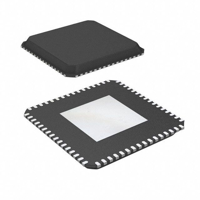
ICGOO电子元器件商城为您提供USB2660-JZX由Microchip设计生产,在icgoo商城现货销售,并且可以通过原厂、代理商等渠道进行代购。 USB2660-JZX价格参考¥询价-¥询价。MicrochipUSB2660-JZX封装/规格:接口 - 专用, 控制器 Interface 64-QFN(9x9)。您可以下载USB2660-JZX参考资料、Datasheet数据手册功能说明书,资料中有USB2660-JZX 详细功能的应用电路图电压和使用方法及教程。
Microchip Technology 的 USB2660-JZX 是一款高度集成的 USB 2.0 集线器控制器,专为需要高性能、低功耗和小尺寸设计的应用场景而设计。该芯片内置 USB 2.0 收发器、PHY 和集线器控制器,支持最多 4 个下行端口,适用于多种嵌入式和消费类电子产品。

其典型应用场景包括:

1. 便携式设备扩展坞:如笔记本电脑、平板电脑或智能手机的 USB 扩展坞,提供多个 USB 接口用于连接外设。

2. 工业控制与嵌入式系统:在工业自动化设备中作为 USB 接口管理芯片,连接多个传感器、执行器或人机界面设备(HMI)。

3. 车载信息系统:用于车载娱乐系统或车载充电器中,实现多设备 USB 充电与数据连接。

4. 智能家电与物联网设备:如智能家居中心、网关设备等,通过集成 USB 集线器功能连接多个外围设备或模块。

5. 医疗设备:用于便携式医疗仪器中,连接多种 USB 接口的诊断或监测设备。

USB2660-JZX 支持低功耗模式、热插拔检测和过流保护,具备良好的稳定性和兼容性,适合对空间和功耗敏感的应用场景。
| 参数 | 数值 |
| 产品目录 | 集成电路 (IC)半导体 |
| 描述 | USB 2.0 FLASH MEDIA CTRLR W/HUBUSB 接口集成电路 Ultra Fast USB 2.0 MF Media Dual SD |
| 产品分类 | |
| 品牌 | Microchip Technology |
| 产品手册 | |
| 产品图片 | |
| rohs | 符合RoHS无铅 / 符合限制有害物质指令(RoHS)规范要求 |
| 产品系列 | 接口 IC,USB 接口集成电路,Microchip Technology USB2660-JZX- |
| 数据手册 | |
| 产品型号 | USB2660-JZX |
| 产品种类 | USB 接口集成电路 |
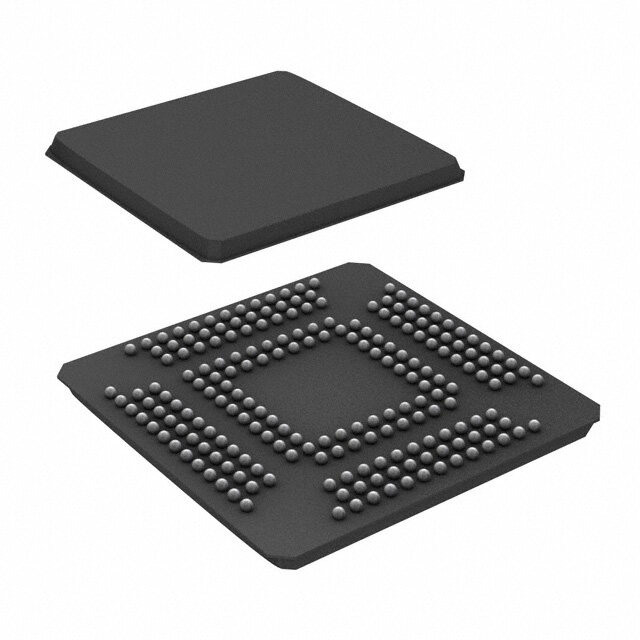
| 供应商器件封装 | 64-QFN(9x9) |
| 包装 | 托盘 |
| 商标 | Microchip Technology |
| 安装类型 | 表面贴装 |
| 安装风格 | SMD/SMT |
| 封装 | Tray |
| 封装/外壳 | 64-VFQFN 裸露焊盘 |
| 封装/箱体 | QFN-64 |
| 工作电源电压 | 3.3 V |
| 工厂包装数量 | 260 |
| 应用 | 控制器 |
| 接口 | - |
| 接口类型 | Serial |
| 最大工作温度 | + 70 C |
| 最小工作温度 | 0 C |
| 标准 | USB 2.0 |
| 标准包装 | 260 |
| 电压-电源 | 3.3V |
| 类型 | Media Controller |
| 速度 | High-Speed |


- 商务部:美国ITC正式对集成电路等产品启动337调查
- 曝三星4nm工艺存在良率问题 高通将骁龙8 Gen1或转产台积电
- 太阳诱电将投资9.5亿元在常州建新厂生产MLCC 预计2023年完工
- 英特尔发布欧洲新工厂建设计划 深化IDM 2.0 战略
- 台积电先进制程称霸业界 有大客户加持明年业绩稳了
- 达到5530亿美元!SIA预计今年全球半导体销售额将创下新高
- 英特尔拟将自动驾驶子公司Mobileye上市 估值或超500亿美元
- 三星加码芯片和SET,合并消费电子和移动部门,撤换高东真等 CEO
- 三星电子宣布重大人事变动 还合并消费电子和移动部门
- 海关总署:前11个月进口集成电路产品价值2.52万亿元 增长14.8%


PDF Datasheet 数据手册内容提取
USB2660/USB2660i Ultra Fast USB 2.0 Hub and Multi-Format Flash Media Controller with Dual SD Interfaces PRODUCT FEATURES Datasheet General Description Features The SMSC USB2660/USB2660i is a USB 2.0 compliant, Hi- Speed hub, card reader, and protocol converter combo (cid:132) Compliance with the following flash media card solution. This fully integrated single chip solution provides USB specifications SD 2.0 / MMC 4.2 / MS 1.43 / MS-Pro 1.02 / expansion and flash card media reader/writer integration. SDIO MS-Pro-HG 1.01 / MS-Duo 1.10 / xD 1.2 bridging is possible with custom firmware. The SMSC USB2660/USB2660i provides an ultra fast interface between a (cid:132) Supports a single external 3.3 V supply source; internal USB host and today’s popular flash media formats. The regulators provide 1.8 V internal core voltage for additional controller allows read/write capability to flash media from the bill of materials and power savings following families: (cid:132) The transaction translator (TT) in the hub supports operation – Secure DigitalTM (SD) of Full-Speed and Low-Speed peripherals – MultiMediaCardTM (MMC) (cid:132) 9 K RAM | 64 K on-chip ROM – Memory Stick® (MS) – xD-Picture CardTM (xD)1 (cid:132) Enhanced EMI rejection and ESD protection performance (cid:132) Hub and flash media reader/writer configuration from a The USB2660/USB2660i offers a versatile, cost-effective, and single source: External I2C® ROM or external SPI ROM energy-efficient hub controller with 2 downstream USB 2.0 ports. This combo solution leverages SMSC’s innovative — Configures internal code using an external I2C EEPROM technology that delivers industry-leading data throughput in mixed-speed USB environments. Average sustained transfer — Supports external code using an SPI Flash EEPROM rates exceeding 35 MB/s are possible2. — Customizable vendor ID, product ID, and language ID if using an external EEPROM Highlights (cid:132) Additional SD/SDIO port for card reader or to host wireless (cid:132) 2 exposed Hi-Speed USB 2.0 downstream ports for external applications such as WiFiTM, Bluetooth®, and GPS peripheral expansion (cid:132) Up to 20 configurable GPIOs for special functions (cid:132) The dedicated flash media reader is internally attached to a 3rd downstream port of the hub as a USB Compound (cid:132) The USB2660 supports the commercial temperature range Device of 0°C to +70°C — a single or multiplexed flash media reader interface (cid:132) The USB2660i supports the industrial temperature range of — a non-multiplexed SD/SDIO interface (slot) for SD card reader -40°C to +85°C or SDIO bridging applications (cid:132) PortMap (cid:132) 64-pin QFN lead-free, RoHS compliant package (9 x 9 mm) — Flexible port mapping and port disable sequencing supports multiple platform designs Applications (cid:132) PortSwap — Programmable USB differential-pair pin locations eases PCB (cid:132) Desktop and mobile PCs design by aligning USB signal traces directly to connectors (cid:132) Printers (cid:132) PHYBoost — Programmable USB transceiver drive strength recovers signal (cid:132) GPS navigation systems integrity (cid:132) Media players/viewers (cid:132) Consumer A/V (cid:132) Set-top boxes 1.For xD-Picture CardTM support, please obtain a user license (cid:132) Industrial products from the xD-Picture Card License Office. 2.Host and media dependent. SMSC USB2660/USB2660i DATASHEET Revision 1.1 (11-05-10)
Ultra Fast USB 2.0 Hub and Multi-Format Flash Media Controller with Dual SD Interfaces Datasheet ORDER NUMBERS: USB2660/USB2660i-JZX for 64-PIN, QFN LEAD-FREE RoHS COMPLIANT PACKAGE THIS PRODUCT MEETS THE HALOGEN MAXIMUM CONCENTRATION VALUES PER IEC61249-2-21. FOR ROHS COMPLIANCE AND ENVIRONMENTAL INFORMATION, PLEASE VISIT WWW.SMSC.COM/ROHS. 80 ARKAY DRIVE, HAUPPAUGE, NY 11788 (631) 435-6000, FAX (631) 273-3123 Copyright © 2010 SMSC or its subsidiaries. All rights reserved. Circuit diagrams and other information relating to SMSC products are included as a means of illustrating typical applications. Consequently, complete information sufficient for construction purposes is not necessarily given. Although the information has been checked and is believed to be accurate, no responsibility is assumed for inaccuracies. SMSC reserves the right to make changes to specifications and product descriptions at any time without notice. Contact your local SMSC sales office to obtain the latest specifications before placing your product order. The provision of this information does not convey to the purchaser of the described semiconductor devices any licenses under any patent rights or other intellectual property rights of SMSC or others. All sales are expressly conditional on your agreement to the terms and conditions of the most recently dated version of SMSC's standard Terms of Sale Agreement dated before the date of your order (the "Terms of Sale Agreement"). The product may contain design defects or errors known as anomalies which may cause the product's functions to deviate from published specifications. Anomaly sheets are available upon request. SMSC products are not designed, intended, authorized or warranted for use in any life support or other application where product failure could cause or contribute to personal injury or severe property damage. Any and all such uses without prior written approval of an Officer of SMSC and further testing and/or modification will be fully at the risk of the customer. Copies of this document or other SMSC literature, as well as the Terms of Sale Agreement, may be obtained by visiting SMSC’s website at http://www.smsc.com. SMSC is a registered trademark of Standard Microsystems Corporation (“SMSC”). Product names and company names are the trademarks of their respective holders. SMSC makes the following part-numbered device available for purchase only by customers who are xD-Picture Card licensees: USB2660/USB2660i. By purchasing or ordering any of such devices, Buyer represents, warrants, and agrees that Buyer is a duly licensed Licensee under an xD-Picture CardTM License Agreement with Fuji Photo Film Co., Ltd., Olympus Optical Co., Ltd., and Toshiba Corporation; and that Buyer will maintain in effect such xD-Picture Card license and will give SMSC reasonable advance notice of any termination or expiration of such xD-Picture Card license, but in no event less than five days advance notice. SMSC may discontinue making such devices available for purchase by Buyer and/or discontinue further deliveries of such devices if such xD-Picture Card license shall expire, terminate, or cease to be in force, or if Buyer is or becomes in default of such xD-Picture Card license. SMSC DISCLAIMS AND EXCLUDES ANY AND ALL WARRANTIES, INCLUDING WITHOUT LIMITATION ANY AND ALL IMPLIED WARRANTIES OF MERCHANTABILITY, FITNESS FOR A PARTICULAR PURPOSE, TITLE, AND AGAINST INFRINGEMENT AND THE LIKE, AND ANY AND ALL WARRANTIES ARISING FROM ANY COURSE OF DEALING OR USAGE OF TRADE. IN NO EVENT SHALL SMSC BE LIABLE FOR ANY DIRECT, INCIDENTAL, INDIRECT, SPECIAL, PUNITIVE, OR CONSEQUENTIAL DAMAGES; OR FOR LOST DATA, PROFITS, SAVINGS OR REVENUES OF ANY KIND; REGARDLESS OF THE FORM OF ACTION, WHETHER BASED ON CONTRACT; TORT; NEGLIGENCE OF SMSC OR OTHERS; STRICT LIABILITY; BREACH OF WARRANTY; OR OTHERWISE; WHETHER OR NOT ANY REMEDY OF BUYER IS HELD TO HAVE FAILED OF ITS ESSENTIAL PURPOSE, AND WHETHER OR NOT SMSC HAS BEEN ADVISED OF THE POSSIBILITY OF SUCH DAMAGES. Revision 1.1 (11-05-10) 2 SMSC USB2660/USB2660i DATASHEET
Ultra Fast USB 2.0 Hub and Multi-Format Flash Media Controller with Dual SD Interfaces Datasheet Table of Contents Chapter1 Overview. . . . . . . . . . . . . . . . . . . . . . . . . . . . . . . . . . . . . . . . . . . . . . . . . . . . . . . . . . 7 Chapter2 Acronyms . . . . . . . . . . . . . . . . . . . . . . . . . . . . . . . . . . . . . . . . . . . . . . . . . . . . . . . . 10 Chapter3 Pin Configuration . . . . . . . . . . . . . . . . . . . . . . . . . . . . . . . . . . . . . . . . . . . . . . . . . 11 Chapter4 Block Diagram . . . . . . . . . . . . . . . . . . . . . . . . . . . . . . . . . . . . . . . . . . . . . . . . . . . . 12 Chapter5 Pin Table. . . . . . . . . . . . . . . . . . . . . . . . . . . . . . . . . . . . . . . . . . . . . . . . . . . . . . . . . 13 5.1 64-Pin Table. . . . . . . . . . . . . . . . . . . . . . . . . . . . . . . . . . . . . . . . . . . . . . . . . . . . . . . . . . . . . . . . . . 13 Chapter6 Pin Descriptions. . . . . . . . . . . . . . . . . . . . . . . . . . . . . . . . . . . . . . . . . . . . . . . . . . . 15 6.1 USB2660/USB2660i Pin Descriptions . . . . . . . . . . . . . . . . . . . . . . . . . . . . . . . . . . . . . . . . . . . . . . 15 6.2 Buffer Type Descriptions . . . . . . . . . . . . . . . . . . . . . . . . . . . . . . . . . . . . . . . . . . . . . . . . . . . . . . . . 22 6.3 Port Power Control. . . . . . . . . . . . . . . . . . . . . . . . . . . . . . . . . . . . . . . . . . . . . . . . . . . . . . . . . . . . . 23 6.4 ROM BOOT Sequence. . . . . . . . . . . . . . . . . . . . . . . . . . . . . . . . . . . . . . . . . . . . . . . . . . . . . . . . . . 25 Chapter7 Pin Reset States . . . . . . . . . . . . . . . . . . . . . . . . . . . . . . . . . . . . . . . . . . . . . . . . . . . 26 7.1 Pin Reset States. . . . . . . . . . . . . . . . . . . . . . . . . . . . . . . . . . . . . . . . . . . . . . . . . . . . . . . . . . . . . . . 26 Chapter8 Configuration Options. . . . . . . . . . . . . . . . . . . . . . . . . . . . . . . . . . . . . . . . . . . . . . 29 8.1 Hub. . . . . . . . . . . . . . . . . . . . . . . . . . . . . . . . . . . . . . . . . . . . . . . . . . . . . . . . . . . . . . . . . . . . . . . . . 29 8.1.1 Hub Configuration Options . . . . . . . . . . . . . . . . . . . . . . . . . . . . . . . . . . . . . . . . . . . . . . . 29 8.1.2 VBus Detect. . . . . . . . . . . . . . . . . . . . . . . . . . . . . . . . . . . . . . . . . . . . . . . . . . . . . . . . . . . 29 8.2 Card Reader. . . . . . . . . . . . . . . . . . . . . . . . . . . . . . . . . . . . . . . . . . . . . . . . . . . . . . . . . . . . . . . . . . 29 8.3 System Configurations . . . . . . . . . . . . . . . . . . . . . . . . . . . . . . . . . . . . . . . . . . . . . . . . . . . . . . . . . . 30 8.3.1 EEPROM/SPI Interface. . . . . . . . . . . . . . . . . . . . . . . . . . . . . . . . . . . . . . . . . . . . . . . . . . 30 8.3.2 EEPROM Data Descriptor. . . . . . . . . . . . . . . . . . . . . . . . . . . . . . . . . . . . . . . . . . . . . . . . 30 8.4 Set bit 7 of bmAttribute to enable the registers in Table8.4. . . . . . . . . . . . . . . . . . . . . . . . . . . . . . 33 8.4.1 EEPROM Data Descriptor Register Descriptions . . . . . . . . . . . . . . . . . . . . . . . . . . . . . . 34 8.4.2 A0h-A7h: Device Power Configuration . . . . . . . . . . . . . . . . . . . . . . . . . . . . . . . . . . . . . . 38 8.4.3 Device ID Strings. . . . . . . . . . . . . . . . . . . . . . . . . . . . . . . . . . . . . . . . . . . . . . . . . . . . . . . 40 8.4.4 Hub Controller Configurations. . . . . . . . . . . . . . . . . . . . . . . . . . . . . . . . . . . . . . . . . . . . . 41 8.4.5 Internal Flash Media Controller Extended Configurations. . . . . . . . . . . . . . . . . . . . . . . . 51 8.4.6 I2C EEPROM. . . . . . . . . . . . . . . . . . . . . . . . . . . . . . . . . . . . . . . . . . . . . . . . . . . . . . . . . . 53 8.4.7 In-Circuit EEPROM Programming. . . . . . . . . . . . . . . . . . . . . . . . . . . . . . . . . . . . . . . . . . 53 8.5 Default Configuration Option . . . . . . . . . . . . . . . . . . . . . . . . . . . . . . . . . . . . . . . . . . . . . . . . . . . . . 54 8.5.1 External Hardware nRESET . . . . . . . . . . . . . . . . . . . . . . . . . . . . . . . . . . . . . . . . . . . . . . 54 8.5.2 USB Bus Reset . . . . . . . . . . . . . . . . . . . . . . . . . . . . . . . . . . . . . . . . . . . . . . . . . . . . . . . . 55 Chapter9 AC Specifications. . . . . . . . . . . . . . . . . . . . . . . . . . . . . . . . . . . . . . . . . . . . . . . . . . 56 9.1 Oscillator/Crystal. . . . . . . . . . . . . . . . . . . . . . . . . . . . . . . . . . . . . . . . . . . . . . . . . . . . . . . . . . . . . . . 56 9.2 Ceramic Resonator. . . . . . . . . . . . . . . . . . . . . . . . . . . . . . . . . . . . . . . . . . . . . . . . . . . . . . . . . . . . . 57 9.3 External Clock. . . . . . . . . . . . . . . . . . . . . . . . . . . . . . . . . . . . . . . . . . . . . . . . . . . . . . . . . . . . . . . . . 57 9.3.1 I2C EEPROM. . . . . . . . . . . . . . . . . . . . . . . . . . . . . . . . . . . . . . . . . . . . . . . . . . . . . . . . . . 57 9.3.2 USB 2.0. . . . . . . . . . . . . . . . . . . . . . . . . . . . . . . . . . . . . . . . . . . . . . . . . . . . . . . . . . . . . . 57 Chapter10 DC Parameters. . . . . . . . . . . . . . . . . . . . . . . . . . . . . . . . . . . . . . . . . . . . . . . . . . . . 58 10.1 Maximum Guaranteed Ratings. . . . . . . . . . . . . . . . . . . . . . . . . . . . . . . . . . . . . . . . . . . . . . . . . . . . 58 10.2 Operating Conditions . . . . . . . . . . . . . . . . . . . . . . . . . . . . . . . . . . . . . . . . . . . . . . . . . . . . . . . . . . . 59 10.3 DC Electrical Characteristics . . . . . . . . . . . . . . . . . . . . . . . . . . . . . . . . . . . . . . . . . . . . . . . . . . . . . 59 SMSC USB2660/USB2660i 3 Revision 1.1 (11-05-10) DATASHEET
Ultra Fast USB 2.0 Hub and Multi-Format Flash Media Controller with Dual SD Interfaces Datasheet 10.4 Capacitance . . . . . . . . . . . . . . . . . . . . . . . . . . . . . . . . . . . . . . . . . . . . . . . . . . . . . . . . . . . . . . . . . . 63 Chapter11 GPIO Usage . . . . . . . . . . . . . . . . . . . . . . . . . . . . . . . . . . . . . . . . . . . . . . . . . . . . . . 64 Chapter12 Package Specifications. . . . . . . . . . . . . . . . . . . . . . . . . . . . . . . . . . . . . . . . . . . . . . 65 12.1 Tape and Reel Specifications. . . . . . . . . . . . . . . . . . . . . . . . . . . . . . . . . . . . . . . . . . . . . . . . . . . . . 66 Revision 1.1 (11-05-10) 4 SMSC USB2660/USB2660i DATASHEET
Ultra Fast USB 2.0 Hub and Multi-Format Flash Media Controller with Dual SD Interfaces Datasheet List of Tables Table5.1 USB2660/USB2660i 64-Pin Table. . . . . . . . . . . . . . . . . . . . . . . . . . . . . . . . . . . . . . . . . . . . . . 13 Table6.1 USB2660/USB2660i Pin Descriptions. . . . . . . . . . . . . . . . . . . . . . . . . . . . . . . . . . . . . . . . . . . 15 Table6.2 USB2660/USB2660i Buffer Type Descriptions . . . . . . . . . . . . . . . . . . . . . . . . . . . . . . . . . . . . 22 Table7.1 Legend for Pin Reset States Table . . . . . . . . . . . . . . . . . . . . . . . . . . . . . . . . . . . . . . . . . . . . . 26 Table7.2 USB2660/USB2660i Reset States Table. . . . . . . . . . . . . . . . . . . . . . . . . . . . . . . . . . . . . . . . . 26 Table8.1 Internal Flash Media Controller Configurations. . . . . . . . . . . . . . . . . . . . . . . . . . . . . . . . . . . . 30 Table8.2 Hub Controller Configurations. . . . . . . . . . . . . . . . . . . . . . . . . . . . . . . . . . . . . . . . . . . . . . . . . 32 Table8.3 Other Internal Configurations. . . . . . . . . . . . . . . . . . . . . . . . . . . . . . . . . . . . . . . . . . . . . . . . . . 32 Table8.4 Internal Flash Media Controller Extended Configurations. . . . . . . . . . . . . . . . . . . . . . . . . . . . 33 Table8.5 Port Map Register for Ports 1 & 2 . . . . . . . . . . . . . . . . . . . . . . . . . . . . . . . . . . . . . . . . . . . . . . 49 Table8.6 Port Map Register for Port 3 . . . . . . . . . . . . . . . . . . . . . . . . . . . . . . . . . . . . . . . . . . . . . . . . . . 50 Table8.7 nRESET Timing for EEPROM Mode. . . . . . . . . . . . . . . . . . . . . . . . . . . . . . . . . . . . . . . . . . . . 54 Table9.1 Crystal Circuit Legend. . . . . . . . . . . . . . . . . . . . . . . . . . . . . . . . . . . . . . . . . . . . . . . . . . . . . . . 56 Table10.1Pin Capacitance. . . . . . . . . . . . . . . . . . . . . . . . . . . . . . . . . . . . . . . . . . . . . . . . . . . . . . . . . . . . 63 Table11.1USB2660/USB2660i GPIO Usage. . . . . . . . . . . . . . . . . . . . . . . . . . . . . . . . . . . . . . . . . . . . . . 64 SMSC USB2660/USB2660i 5 Revision 1.1 (11-05-10) DATASHEET
Ultra Fast USB 2.0 Hub and Multi-Format Flash Media Controller with Dual SD Interfaces Datasheet List of Figures Figure3.1 USB2660/USB2660i 64-Pin QFN. . . . . . . . . . . . . . . . . . . . . . . . . . . . . . . . . . . . . . . . . . . . . . 11 Figure4.1 USB2660/USB2660i Block Diagram . . . . . . . . . . . . . . . . . . . . . . . . . . . . . . . . . . . . . . . . . . . 12 Figure6.1 Port Power Control with USB Power Switch . . . . . . . . . . . . . . . . . . . . . . . . . . . . . . . . . . . . . 23 Figure6.2 Port Power Control with a Single Poly Fuse and Multiple Loads. . . . . . . . . . . . . . . . . . . . . . 24 Figure6.3 Port Power with Ganged Control with Poly Fuse. . . . . . . . . . . . . . . . . . . . . . . . . . . . . . . . . . 24 Figure6.4 SPI ROM Connection. . . . . . . . . . . . . . . . . . . . . . . . . . . . . . . . . . . . . . . . . . . . . . . . . . . . . . . 25 Figure6.5 I2C Connection. . . . . . . . . . . . . . . . . . . . . . . . . . . . . . . . . . . . . . . . . . . . . . . . . . . . . . . . . . . . 25 Figure7.1 Pin Reset States . . . . . . . . . . . . . . . . . . . . . . . . . . . . . . . . . . . . . . . . . . . . . . . . . . . . . . . . . . 26 Figure8.1 nRESET Timing for EEPROM Mode . . . . . . . . . . . . . . . . . . . . . . . . . . . . . . . . . . . . . . . . . . . 54 Figure9.1 Typical Crystal Circuit . . . . . . . . . . . . . . . . . . . . . . . . . . . . . . . . . . . . . . . . . . . . . . . . . . . . . . 56 Figure9.2 Capacitance Formulas. . . . . . . . . . . . . . . . . . . . . . . . . . . . . . . . . . . . . . . . . . . . . . . . . . . . . . 56 Figure9.3 Ceramic Resonator Usage with SMSC IC. . . . . . . . . . . . . . . . . . . . . . . . . . . . . . . . . . . . . . . 57 Figure10.1 Supply Rise Time Model . . . . . . . . . . . . . . . . . . . . . . . . . . . . . . . . . . . . . . . . . . . . . . . . . . . . 58 Figure12.1 USB2660/USB2660i 64-Pin QFN. . . . . . . . . . . . . . . . . . . . . . . . . . . . . . . . . . . . . . . . . . . . . . 65 Figure12.2 64-Pin Package Tape Specifications. . . . . . . . . . . . . . . . . . . . . . . . . . . . . . . . . . . . . . . . . . . 66 Figure12.3 64-Pin Package Reel Specifications . . . . . . . . . . . . . . . . . . . . . . . . . . . . . . . . . . . . . . . . . . . 67 Revision 1.1 (11-05-10) 6 SMSC USB2660/USB2660i DATASHEET
Ultra Fast USB 2.0 Hub and Multi-Format Flash Media Controller with Dual SD Interfaces Datasheet Chapter 1 Overview The SMSC USB2660/USB2660i is an integrated USB 2.0 compliant, Hi-Speed hub, card reader, and protocol converter combo solution. This combo solution supports today’s popular multi-format flash media cards. This multi-format flash media controller and USB hub combo features two exposed downstream USB ports available for external peripheral expansion. The dedicated flash media reader/writer is internally attached to a third downstream port of the hub as a USB Compound Device which supports the following two interfaces: One interface is multiplexed for xD-Picture Card, Memory Stick, Secure Digital/MultiMediaCard, and SD/Secure Digital Input/Output. The other interface is dedicated to a second SD card slot for SDIO bridging applications. SDIO bridging is possible with custom firmware. The USB2660/USB2660i will attach to an upstream port as a Full-Speed hub or as a Full-/Hi-Speed hub. The hub supports Low-Speed, Full-Speed, and Hi-Speed (if operating as a Hi-Speed hub) downstream devices on all of the enabled downstream ports. All required resistors on the USB ports are integrated into the hub. This includes all series termination resistors on D+ and D– pins and all required pull-down and pull-up resistors. The over- current sense inputs for the downstream facing ports have internal pull-up resistors. The USB2660/USB2660i includes programmable features such as: PortMap which provides flexible port mapping and disable sequences. The downstream ports of a USB2660/USB2660i hub can be reordered or disabled in any sequence to support multiple platform designs with minimum effort. For any port that is disabled, the USB2660/USB2660i automatically reorders the remaining ports to match the USB host controller’s port numbering scheme. PortSwap which adds per-port programmability to USB differential- pair pin locations. PortSwap allows direct alignment of USB signals (D+/D-) to connectors avoiding uneven trace length or crossing of the USB differential signals on the PCB. PHYBoost which enables four programmable levels of USB signal drive strengths in downstream port transceivers. PHYBoost attempts to restore USB signal integrity. The diagram on the right shows an example of Hi-Speed USB eye diagrams before (PHYBoost at 0%) and after (PHYBoost at 12%) signal integrity restoration in a compromised system environment. SMSC USB2660/USB2660i 7 Revision 1.1 (11-05-10) DATASHEET
Ultra Fast USB 2.0 Hub and Multi-Format Flash Media Controller with Dual SD Interfaces Datasheet Hardware Features (cid:132) Single chip hub and flash media controller combo (cid:132) USB2660 supports the commercial temperature range of 0°C to +70°C (cid:132) USB2660i supports the industrial temperature range of -40°C to +85°C (cid:132) Transaction translator (TT) in the hub supports operation of FS and LS peripherals (cid:132) Full power management with individual or ganged power control of each downstream port (cid:132) Optional support for external firmware access via SPI interface (cid:132) Onboard 24 MHz crystal driver circuit (cid:132) Optional external 24 MHz clock input which must be a 1.8 V signal (cid:132) Code execution via SPI ROM which must meet - 30 MHz or 60 MHz operation support - Single bit or dual bit mode support - Mode 0 or mode 3 SPI support Compliance with the following flash media card specifications: (cid:132) Secure Digital 2.0 / MultiMediaCard 4.2 - SD 2.0, SD-HS, SD-HC - TransFlash™ and reduced form factor media - 1/4/8 bit MMC 4.2 (cid:132) Memory Stick 1.43 (cid:132) Memory Stick Pro Format 1.02 (cid:132) Memory Stick Pro-HG Duo Format 1.01 - Memory Stick, MS Duo, MS-HS, MS Pro-HG, MS Pro (cid:132) Memory Stick Duo 1.10 (cid:132) xD-Picture Card 1.2 (cid:132) Up to 20 GPIOs: Configuration and polarity for special function use - The number of actual GPIOs depends on the implementation configuration used - Two GPIOs available with up to 200 mA drive and protected “fold-back” short circuit current (cid:132) 8051 8-bit microprocessor - 60 MHz - single cycle execution - 64 KB ROM | 9 KB RAM (cid:132) Integrated regulator for 1.8 V core operation Software Features (cid:132) Hub and flash media reader/writer configuration from a single source: External I2C ROM or external SPI ROM (cid:132) If the OEM is using an external EEPROM or an external SPI ROM, the following features are available: - Customizable vendor ID, product ID, and device ID - 12-hex digits maximum for the serial number string - 28-character manufacturer ID and product strings for the flash media reader/writer Revision 1.1 (11-05-10) 8 SMSC USB2660/USB2660i DATASHEET
Ultra Fast USB 2.0 Hub and Multi-Format Flash Media Controller with Dual SD Interfaces Datasheet OEM Selectable Hub Features A default configuration is available in the USB2660/USB2660i following a reset. The USB2660/USB2660i may also be configured by an external I2C EEPROM or via external SPI ROM flash. (cid:132) Compound Device support on a port-by-port basis - a port is permanently hardwired to a downstream USB peripheral device (cid:132) Select over-current sensing and port power control on an individual or ganged (all ports together) basis to match the OEM’s choice of circuit board component selection (cid:132) Port power control and over-current detection/delay features (cid:132) Configure the delay time for filtering the over-current sense inputs (cid:132) Configure the delay time for turning on downstream port power (cid:132) Bus- or self-powered selection (cid:132) Hub port disable or non-removable configurations (cid:132) Flexible port mapping and disable sequencing supports multiple platform designs (cid:132) Programmable USB differential-pair pin location eases PCB layout by aligning USB signal lines directly to connectors (cid:132) Programmable USB signal drive strength recovers USB signal integrity using 4 levels of signal drive strength (cid:132) Indicate the maximum current that the 2-port hub consumes from the USB upstream port (cid:132) Indicate the maximum current required for the hub controller SMSC USB2660/USB2660i 9 Revision 1.1 (11-05-10) DATASHEET
Ultra Fast USB 2.0 Hub and Multi-Format Flash Media Controller with Dual SD Interfaces Datasheet Chapter 2 Acronyms ACK: Handshake packet (positive acknowledgement) EOP: End of Packet EOF: End of (micro) Frame FM: Flash Media FMC: Flash Media Controller FS: Full-Speed Device LS: Low-Speed Device HS: Hi-Speed Device I2C®: Inter-Integrated Circuit1 MMC: MultiMediaCard MS: Memory Stick MSC: Memory Stick Controller OCS: Over-current Sense PHY: Physical Layer PLL: Phase-Locked Loop RXD: Received eXchange Data SD: Secure Digital SDC: Secure Digital Controller TXD: Transmit eXchange Data UART: Universal Asynchronous Receiver-Transmitter UCHAR: Unsigned Character UINT: Unsigned Integer Standard Microsystems is a registered trademark and SMSC is a trademark of Standard Microsystems Corporation. Other product and company names are trademarks or registered trademarks of their respective holders. *Note: In order to develop, make, use, or sell readers and/or other products using or incorporating any of the SMSC devices made the subject of this document or to use related SMSC software programs, technical information and licenses under patent and other intellectual property rights from or through various persons or entities, including without limitation media standard companies, forums, and associations, and other patent holders may be required. These media standard companies, forums, and associations include without limitation the following: Sony Corporation (Memory Stick, Memory Stick Pro); SD3 LLC (Secure Digital); MultiMedia Card Association (MultiMediaCard); the SSFDC Forum (SmartMedia); the Compact Flash Association (Compact Flash); and Fuji Photo Film Co., Ltd., Olympus Optical Co., Ltd., and Toshiba Corporation (xD-Picture Card). SMSC does not make such licenses or technical information available; does not promise or represent that any such licenses or technical information will actually be obtainable from or through the various persons or entities (including the media standard companies, forums, and associations), or with respect to the terms under which they may be made available; and is not responsible for the accuracy or sufficiency of, or otherwise with respect to, any such technical information. SMSC's obligations (if any) under the Terms of Sale Agreement, or any other agreement with any customer, or otherwise, with respect to infringement, including without limitation any obligations to defend or settle claims, to reimburse for costs, or to pay damages, shall not apply to any of the devices made the subject of this document or any software programs related to any of such devices, or to any combinations involving any of them, with respect to infringement or claimed infringement of any existing or future patents related to solid state disk or other flash memory technology or applications (“Solid State Disk Patents”). By making any purchase of any of the devices made the subject of this document, the customer represents, warrants, and agrees that it has obtained all necessary licenses under then-existing Solid State Disk Patents for the manufacture, use and sale of solid state disk and other flash memory products and that the customer will timely obtain at no cost or expense to SMSC all necessary licenses under Solid State Disk Patents; that the manufacture and testing by or for SMSC of the units of any of the devices made the subject of this document which may be sold to the customer, and any sale by SMSC of such units to the customer, are valid exercises of the customer's rights and licenses under such Solid State Disk Patents; that SMSC shall have no obligation for royalties or otherwise under any Solid State Disk Patents by reason of any such manufacture, use, or sale of such units; and that SMSC shall have no obligation for any costs or expenses related to the customer's obtaining or having obtained rights or licenses under any Solid State Disk Patents. SMSC MAKES NO WARRANTIES, EXPRESS, IMPLIED, OR STATUTORY, IN REGARD TO INFRINGEMENT OR OTHER VIOLATION OF INTELLECTUAL PROPERTY RIGHTS. SMSC DISCLAIMS AND EXCLUDES ANY AND ALL WARRANTIES AGAINST INFRINGEMENT AND THE LIKE. No license is granted by SMSC expressly, by implication, by estoppel or otherwise, under any patent, trademark, copyright, mask work right, trade secret, or other intellectual property right. **To obtain this software program the appropriate SMSC Software License Agreement must be executed and in effect. Forms of these Software License Agreements may be obtained by contacting SMSC. 1.I2C is a registered trademark of Philips Corporation. Revision 1.1 (11-05-10) 10 SMSC USB2660/USB2660i DATASHEET
Ultra Fast USB 2.0 Hub and Multi-Format Flash Media Controller with Dual SD Interfaces Datasheet Chapter 3 Pin Configuration 6 7 D D 1) D_ D_ NC VDD33 NC SD2_WP / GPIO17 GPIO2 / RXD GPIO10 (CRD_PWR VDD33 SD1_D2 / xD_D5 SD1_D3 / MS_D3 / x GPIO12 / MS_INS SD1_D4 / MS_D2 / x GPIO14 / xD_nCD xD_nB/R xD_nRE xD_nCE VDD33 8 7 6 5 4 3 2 1 0 9 8 7 6 5 4 3 4 4 4 4 4 4 4 4 4 3 3 3 3 3 3 3 SPI_CE_n 49 32 SD1_CMD / MS_D0 / xD_CLE SPI_CLK / GPIO4 / SCL 50 31 SD1_D5 / MS_D1 / xD_ALE SPI_DO / GPIO5 / SDA / SPI_SPD_SEL 51 30 xD_nWE SPI_DI 52 29 SD1_CLK / MS_BS / xD_nWP GPIO1 / LED / TXD 53 28 SD1_D6 / MS_D7 / xD_D0 nRESET 54 27 SD1_D7 / MS_D6 / xD_D1 VBUS_DET 55 26 SD1_D0 / MS_D4 / xD_D2 SMSC TEST 56 25 SD1_D1 / MS_D5 / xD_D3 USB2660/USB2660i VDD33 57 24 VDD33 (Top View QFN-64) USBUP_DP 58 23 CRFILT USBUP_DM 59 22 GPIO15 / SD1_nCD XTAL2 60 21 GPIO6 / SD1_WP / MS_SCLK / xD_D4 XTAL1 (CLKIN) 61 20 SD2_D2 / GPIO20 PLLFILT 62 19 SD2_D3 / GPIO21 Ground Pad RBIAS 63 (must be connected to VSS) 18 SD2_D4 / GPIO22 VDD33 64 17 SD2_CMD / GPIO27 0 1 2 3 4 5 6 1 2 3 4 5 6 7 8 9 1 1 1 1 1 1 1 USBDN_DM2 USBDN_DP2 USBDN_DM3 USBDN_DP3 VDD33 PRTCTL2 PRTCTL3 SD2_nCD / GPIO16 SD2_D1 / GPIO19 SD2_D0 / GPIO18 SD2_D7 / GPIO25 SD2_D6 / GPIO24 SD2_CLK / GPIO26 VDD33 PIO8 (CRD_PWR2) SD2_D5 / GPIO23 G Indicates pins on the bottom of the device. Figure3.1 USB2660/USB2660i 64-Pin QFN SMSC USB2660/USB2660i 11 Revision 1.1 (11-05-10) DATASHEET
Ultra Fast USB 2.0 Hub and Multi-Format Flash Media Controller with Dual SD Interfaces Datasheet Chapter 4 Block Diagram 2) R1) R W W P P _ _ D PI (4 pins) PIO8 (CRD PIO10 (CR 20 pins S G G or ct et ne kn 8051PROCESSOR SPI PWR_FET1 PWR_FET0GPIOsGPIO Program Memory I/O Bus XDATA BRIDGE+ BUS ARBITER BUS NTFCAUTO_CBW PROC BUS FMDUINTFCCTL FMI SD/SD/MSxD*MMC/MMCSDIO SD/MMC SocFlash Media Cards SDIO Interco(require combo socket) I 24 MHz Crystal Serial PLLInterface SFR RAM ControllerRAM6 KADDRMAP64 K ROM Port Controller EP0 TXEP0 RX 3 KRAMtotal EP2 RXEP2 TX BUS SIEBRIDGEINTFCCTL TM*For xD-Picture Card support, please obtain a user license from the xD-Picture Card License Office. B 1.8 V 3.3 V 1.8 V Reg Serial Interface Engine TransactionTranslator Port Re-Ordering Logic Port #2OC SensePHYSwitch Driver USB DataOC Sense/DownstreamPwr Switch To UpstreamUpstream USVDataBUS Bus-Power Upstream Detect/PHYV PulseBUS Repeater 1.8 V Reg VDDCR Routing & Port #3OC SensePHYSwitch Driver SB DataOC Sense/wnstreamPwr Switch Uo D V 3 3. Figure4.1 USB2660/USB2660i Block Diagram Revision 1.1 (11-05-10) 12 SMSC USB2660/USB2660i DATASHEET
Ultra Fast USB 2.0 Hub and Multi-Format Flash Media Controller with Dual SD Interfaces Datasheet Chapter 5 Pin Table 5.1 64-Pin Table Table5.1 USB2660/USB2660i 64-Pin Table SECURE DIGITAL / MEMORY STICK / xD INTERFACE (18 PINS) SD1_D7 / SD1_D6 / SD1_D5 / SD1_D4 / MS_D6 / MS_D7 / MS_D1 / MS_D2 / xD_D1 xD_D0 xD_ALE xD_D7 SD1_D3 / SD1_D1 / SD1_D0 / SD1_D2 / MS_D3 / MS_D5 / MS_D4 / xD_D5 xD_D6 xD_D3 xD_D2 SD1_CLK / SD1_CMD / GPIO15 / GPIO12 / MS_BS / MS_D0 / SD1_nCD MS_INS xD_ nWP xD_CLE GPIO6 / SD1_WP / GPIO14 / xD_nB/R xD_nRE MS_SCLK / xD_nCD xD_D4 xD_nCE xD_nWE SECOND SECURE DIGITAL INTERFACE (12 PINS) SD2_D7 / SD2_D6 / SD2_D5 / SD2_D4 / GPIO25 GPIO24 GPIO23 GPIO22 SD2_D3 / SD2_D2 / SD2_D1 / SD2_D0 / GPIO21 GPIO20 GPIO19 GPIO18 SD2_nCD / SD2_CLK / SD2_CMD / SD2_WP / GPIO16 GPIO26 GPIO27 GPIO17 USB INTERFACE (5 PINS) USBUP_DP USBUP_DM XTAL1 (CLKIN) XTAL2 RBIAS 2-PORT USB INTERFACE (7 PINS) USBDN_DP2 USBDN_DM2 PRTCTL2 PRTCTL3 USBDN_DP3 USBDN_DM3 VBUS_DET SMSC USB2660/USB2660i 13 Revision 1.1 (11-05-10) DATASHEET
Ultra Fast USB 2.0 Hub and Multi-Format Flash Media Controller with Dual SD Interfaces Datasheet Table5.1 USB2660/USB2660i 64-Pin Table (continued) SPI INTERFACE (4 PINS) SPI_DO / SPI_CLK / GPIO5 / SPI_CE_n GPIO4 / SPI_DI SDA / SCL SPI_SPD_SEL MISC (8 PINS) GPIO1 / GPIO2 / nRESET TEST LED / RXD TXD GPIO8 (CRD_PWR2) GPIO10 (CRD_PWR1) (2) NC POWER (10 PINS) (8) VDD33 CRFILT PLLFILT TOTAL 64 Revision 1.1 (11-05-10) 14 SMSC USB2660/USB2660i DATASHEET
Ultra Fast USB 2.0 Hub and Multi-Format Flash Media Controller with Dual SD Interfaces Datasheet Chapter 6 Pin Descriptions This section provides a detailed description of each signal. The signals are arranged in functional groups according to their associated interface. The pin descriptions below are applied when using the internal default firmware and can be referenced in Chapter8, "Configuration Options," on page29. Please reference Chapter2, "Acronyms," on page10 for a list of the acronyms used. The “n” symbol in the signal name indicates that the active, or asserted, state occurs when the signal is at a low voltage level. When “n” is not present in the signal name, the signal is asserted at a high voltage level. The terms assertion and negation are used exclusively. This is done to avoid confusion when working with a mixture of “active low” and “active high” signals. The term assert, or assertion, indicates that a signal is active, independent of whether that level is represented by a high or low voltage. The term negate, or negation, indicates that a signal is inactive. 6.1 USB2660/USB2660i Pin Descriptions Table6.1 USB2660/USB2660i Pin Descriptions 64-PIN BUFFER QFN TYPE SYMBOL (Table6.2) DESCRIPTION SECURE DIGITAL INTERFACE SD1_D[7:0] 27 I/O8PU Secure Digital Data 7-0 28 31 These are the bi-directional data signals SD_D0 - SD_D7 with weak 38 pull-up resistors. 40 41 25 26 SD1_CLK 29 O8 Secure Digital Clock This is an output clock signal to the SD/MMC device. SD1_CMD 32 I/O8PU Secure Digital Command This is a bi-directional signal that connects to the CMD signal of the SD/MMC device. The bi-directional signal has a weak internal pull-up resistor. GPIO15 / 22 I/O6 This general purpose pin may be used either as input, edge sensitive interrupt input, or output. Custom firmware is required to activate this function. SD1_nCD I/O8PU Secure Digital Card Detect GPIO This is a GPIO designated by the default firmware as the Secure Digital card detection pin and has an internal pull-up. SMSC USB2660/USB2660i 15 Revision 1.1 (11-05-10) DATASHEET
Ultra Fast USB 2.0 Hub and Multi-Format Flash Media Controller with Dual SD Interfaces Datasheet Table6.1 USB2660/USB2660i Pin Descriptions (continued) 64-PIN BUFFER QFN TYPE SYMBOL (Table6.2) DESCRIPTION GPIO6 / 21 I/O6 This general purpose pin may be used either as input, edge sensitive interrupt input, or output. Custom firmware is required to activate this function. SD1_WP I/O8 Secure Digital Write Protected GPIO This is a GPIO designated by the default firmware as the Secure Digital card mechanical write protect detect pin. SECOND SECURE DIGITAL INTERFACE SD2_D[7:0] / 11 I/O8PU SD2 Data 7-0 12 16 These are the bi-directional data signals SD2_D0 - SD2_D7 and have 18 weak pull-up resistors. 19 GPIO[25:18] 20 I/O6 These general purpose pin may be used either as input, edge sensitive 9 interrupt input, or output. Custom firmware is required to activate this 10 function. SD2_CLK / 13 O8 SD2 Clock GPIO This is an output clock signal designated by the default firmware to the SD2/MMC device. GPIO26 I/O6 This general purpose pin may be used either as input, edge sensitive interrupt input, or output. Custom firmware is required to activate this function. SD2_CMD / 17 I/O8PU SD2 Command GPIO This is a bi-directional signal designated by the default firmware that connects to the CMD signal of the SD2/MMC device. The bi-directional signal has a weak internal pull-up resistor. GPIO27 I/O6 This general purpose pin may be used either as input, edge sensitive interrupt input, or output. Custom firmware is required to activate this function. SD2_nCD / 8 I/O8 SD2 Card Detect GPIO This is a GPIO designated by the default firmware as the second Secure Digital card detection pin and has an internal pull-up. GPIO16 I/O6 This general purpose pin may be used either as input, edge sensitive interrupt input, or output. Custom firmware is required to activate this function. SD2_WP / 45 I/O8 SD2 Write Protected GPIO This is a GPIO designated by the default firmware as the second Secure Digital card interface mechanical write detect pin. GPIO17 I/O6 This general purpose pin may be used either as input, edge sensitive interrupt input, or output. Custom firmware is required to activate this function. Revision 1.1 (11-05-10) 16 SMSC USB2660/USB2660i DATASHEET
Ultra Fast USB 2.0 Hub and Multi-Format Flash Media Controller with Dual SD Interfaces Datasheet Table6.1 USB2660/USB2660i Pin Descriptions (continued) 64-PIN BUFFER QFN TYPE SYMBOL (Table6.2) DESCRIPTION MEMORY STICK INTERFACE MS_BS 29 O8 Memory Stick Bus State This pin is connected to the bus state pin of the MS device. It is used to control the Bus States 0, 1, 2, and 3 (BS0, BS1, and BS3) of the MS device. GPIO12 / 39 I/O6 This general purpose pin may be used either as input, edge sensitive interrupt input, or output. Custom firmware is required to activate this function. MS_INS IPU Memory Stick Card Insertion GPIO This is a GPIO designated by the default firmware as the Memory Stick card detection pin and has a weak internal pull-up resistor. MS_SCLK 21 O8 Memory Stick System Clock This pin is an output clock signal to the MS device. MS_D[7:0] 28 I/O8PD Memory Stick System Data In/Out 27 25 These pins are the bi-directional data signals for the MS device. In 26 serial mode, the most significant bit (MSB) of each byte is transmitted 40 first by either MSC or MS device on MS_D0. 38 31 MS_D0, MS_D2, and MS_D3 have weak pull-down resistors. MS_D1 32 has a pull-down resistor if in parallel mode, otherwise it is disabled. In 4- or 8-bit parallel modes, all MS_D7 - MS_D0 signals have weak pull- down resistors. xD-PICTURE CARD INTERFACE xD_D[7:0] 38 I/O8PD xD-Picture Card Data 7-0 40 41 These pins are the bi-directional data signals xD_D7 - xD_D0 and have 21 weak internal pull-down resistors. 25 26 27 28 xD_ALE 31 O8PD xD-Picture Card Address Strobe This pin is an active high Address Latch Enable (ALE) signal for the xD device. This pin has a weak pull-down resistor that is permanently enabled. xD_nB/R 36 IPU xD-Picture Card Busy or Data Ready This pin is connected to the BSY/RDY pin of the xD-Picture Card device. When using the internal FET, this pin has an internal weak pull-up resistor that is tied to the output of the internal power FET. If an external FET is used (the internal FET is disabled), then the internal pull-up is not available (an external pull-up is required). SMSC USB2660/USB2660i 17 Revision 1.1 (11-05-10) DATASHEET
Ultra Fast USB 2.0 Hub and Multi-Format Flash Media Controller with Dual SD Interfaces Datasheet Table6.1 USB2660/USB2660i Pin Descriptions (continued) 64-PIN BUFFER QFN TYPE SYMBOL (Table6.2) DESCRIPTION xD_nCE 34 O8PU xD-Picture Card Chip Enable This pin is an active low chip enable signal for the xD-Picture Card device. When using the internal FET, this pin has an internal weak pull-up resistor that is tied to the output of the internal power FET. If an external FET is used (internal FET is disabled), then the internal pull-up is not available (an external pull-up is required). xD_CLE 32 O8PD xD-Picture Card Command Strobe This pin is an active high Command Latch Enable signal for the xD device. This pin has a weak pull-down resistor that is permanently enabled. GPIO14 / 37 I/O6 This general purpose pin may be used either as input, edge sensitive interrupt input, or output. Custom firmware is required to activate this function. xD_nCD I/O8 xD-Picture Card Detection GPIO This is a GPIO designated by the default firmware as the xD-Picture Card detection pin. xD_nRE 35 O8PU xD-Picture Card Read Enable This pin is an active low read strobe signal for the xD-Picture Card device. When using the internal FET, this pin has an internal weak pull-up resistor that is tied to the output of the internal power FET. If an external FET is used (internal FET is disabled), then the internal pull-up is not available (an external pull-up is required). xD_nWE 30 O8PU xD-Picture Card Write Enable This pin is an active low write strobe signal for the xD-Picture Card device. When using the internal FET, this pin has an internal weak pull-up resistor that is tied to the output of the internal power FET. If an external FET is used (internal FET is disabled), then the internal pull-up is not available (an external pull-up is required). xD_nWP 29 O8PD xD-Picture Card Write Protect This pin is an active low write protect signal for the xD-Picture Card device. This pin has a weak pull-down resistor that is permanently enabled. Revision 1.1 (11-05-10) 18 SMSC USB2660/USB2660i DATASHEET
Ultra Fast USB 2.0 Hub and Multi-Format Flash Media Controller with Dual SD Interfaces Datasheet Table6.1 USB2660/USB2660i Pin Descriptions (continued) 64-PIN BUFFER QFN TYPE SYMBOL (Table6.2) DESCRIPTION USB INTERFACE USBUP_DM 59 I/O-U USB Bus Data USBUP_DP 58 These pins connect to the upstream USB bus data signals (host port or upstream hub). USBUP_DM and USBUP_DP can be swapped using the PortSwap feature (See Section 8.4.4.20, "F1h: Port Swap," on page48). USBDN_DM 3 I/O-U USB Bus Data [3:2] 1 USBDN_DP 4 These pins connect to the downstream USB bus data signals and can [3:2] 2 be swapped using the PortSwap feature (See Section 8.4.4.20, "F1h: Port Swap," on page48). PRTCTL[3:2] 7 I/OD6 USB Power Enable 6 PU As an output, these pins enable power to downstream USB peripheral devices and have weak internal pull-up resistors. See Section 6.3, "Port Power Control" for diagram and usage instructions. As an input, when the power is enabled, these pins monitor the over- current condition. When an over-current condition is detected, the pins turn the power off. VBUS_DET 55 I Detect Upstream VBUS Power Detects the state of upstream VBUS power. The hub monitors VBUS_DET to determine when to assert the internal D+ pull-up resistor (signaling a connect event). When designing a detachable hub, connect this pin to the VBUS power pin of the USB port that is upstream of the hub. For self-powered applications with a permanently attached host, this pin should be pulled up, typically to VDD33. VBUS is a 3.3 volt input. A resistor divider must be used if connecting to 5 volts of USB power. RBIAS 63 I-R USB Transceiver Bias A 12.0 kΩ, ±1.0% resistor is attached from VSS to this pin in order to set the transceiver's internal bias currents. XTAL1 (CLKIN) 61 ICLKx 24 MHz Crystal Input or External Clock Input This pin can be connected to one terminal of the crystal or it can be connected to an external 24 MHz clock when a crystal is not used. XTAL2 60 OCLKx 24 MHz Crystal Output This is the other terminal of the crystal, or it is left open when an external clock source is used to drive XTAL1(CLKIN). SPI INTERFACE SPI_CE_n 49 O12 SPI Chip Enable This is the active low chip enable output. If the SPI interface is enabled, this pin must be driven high in power down states. SMSC USB2660/USB2660i 19 Revision 1.1 (11-05-10) DATASHEET
Ultra Fast USB 2.0 Hub and Multi-Format Flash Media Controller with Dual SD Interfaces Datasheet Table6.1 USB2660/USB2660i Pin Descriptions (continued) 64-PIN BUFFER QFN TYPE SYMBOL (Table6.2) DESCRIPTION SPI_CLK / 50 I/O12 This is the SPI clock out to the serial ROM. See Section 6.4, "ROM BOOT Sequence" for diagram and usage instructions. During reset, drive this pin low. GPIO4 / I/O6 This pin may be used either as input, edge sensitive interrupt input, or output. Custom firmware is required to activate this function. SCL When configured, this is the I2C EEPROM clock pin. SPI_DO / 51 I/O12 This is the data out for the SPI port. See Section 6.4, "ROM BOOT Sequence" for diagram and usage instructions. GPIO5 / I/O6 This pin may be used either as input, edge sensitive interrupt input, or output. Custom firmware is required to activate this function. SDA / This pin is the data pin when the device is connected to the optional I2C EEPROM. SPI_SPD_SEL I/O12 This pin is used to select the speed of the SPI interface. During nRESET assertion, this pin will be tri-stated with the weak pull-down resistor enabled. When nRESET is negated, the value on the pin will be internally latched, and the pin will revert to SPI_DO functionality, the internal pull-down will be disabled. ‘0’ = 30 MHz (No external resistor should be applied.) ‘1’ = 60 MHz (A 10 K external pull-up resistor must be applied.) If the latched value is '1', then the pin is tri-stated when the chip is in the suspend state. If the latched value is '0', then the pin is driven low during a suspend state. SPI_DI 52 I/O12PD This is the data in to the controller from the ROM. This pin has a weak internal pull-down applied at all times to prevent floating. MISC GPIO1 / 53 I/O6 General Purpose I/O This pin may be used either as input, edge sensitive interrupt input, or output. Custom firmware is required to activate this function. LED / GPIO1 can be used as an LED output. TXD This signal can be configured as the TXD output of the internal UART. Custom firmware is required to activate this function. GPIO2 / 44 I/O6 This pin may be used either as input, edge sensitive interrupt input, or output. Custom firmware is required to activate this function. RXD This signal can be configured as input to the RXD of the internal UART. Custom firmware is required to activate this function. Revision 1.1 (11-05-10) 20 SMSC USB2660/USB2660i DATASHEET
Ultra Fast USB 2.0 Hub and Multi-Format Flash Media Controller with Dual SD Interfaces Datasheet Table6.1 USB2660/USB2660i Pin Descriptions (continued) 64-PIN BUFFER QFN TYPE SYMBOL (Table6.2) DESCRIPTION GPIO8 15 I/O200 Card power drive: 3.3 V (100 mA or 200 mA) (CRD_PWR2) This pin specifically powers the second Secure Digital interface (slot). If card power is not being used to power the second SD interface, this pin may be used as a GPIO. Please reference Section 8.4.5.9, "147h-14Bh: Device to LUN Mapping," on page52. GPIO10 43 I/O200 Card power drive: 3.3 V (100 mA or 200 mA) (CRD_PWR1) This pin powers the multiplexed flash media interface (slot) for xD, MS, and SD/MMC. If card power is not being used to power the multiplexed flash media interface, this pin may be used as a GPIO. Please reference Section 8.4.2.3, "A4h-A5h: Smart Media Device Power Configuration," on page39. nRESET 54 IS RESET Input The system uses this active low signal reset the chip. The active low pulse should be at least 1 μs wide. TEST 56 I TEST Input Tie this pin to ground for normal operation. DIGITAL / POWER / GROUND CRFILT 23 VDD Core Regulator Filter Capacitor This pin requires a 1.0 μF (or greater) ± 20% (ESR <0.1Ω) capacitor to VSS. PLLFILT 62 Phase-locked Loop Regulator Filter Capacitor This pin requires 1.0 μF (or greater) ± 20% (ESR <0.1Ω) capacitor to VSS. VDD33 5 3.3 V Power and Regulator Input 14 24 Please refer to Chapter10, "DC Parameters," on page58 for more 33 information. 42 47 Pins 24 and 64 require external bypass capacitors of 4.7 μF minimum. 57 64 VSS ePad The ground pad is the only VSS for the device and must be tied to ground with multiple vias. NC 46 No Connect pins 48 No trace or signal should be routed/attached to these pins. SMSC USB2660/USB2660i 21 Revision 1.1 (11-05-10) DATASHEET
Ultra Fast USB 2.0 Hub and Multi-Format Flash Media Controller with Dual SD Interfaces Datasheet 6.2 Buffer Type Descriptions Table6.2 USB2660/USB2660i Buffer Type Descriptions BUFFER DESCRIPTION I Input. IPU Input with weak internal pull-up. IS Input with Schmitt trigger. I/O6 Input/output buffer with 6 mA sink and 6 mA source. I/OD6PU Input/open drain output buffer with a 6 mA sink. O8 Output buffer with an 8 mA sink and an 8 mA source. O8PD Output buffer with an 8 mA sink and an 8 mA source with a weak internal pull-down resistor. O8PU Output buffer with an 8 mA sink and an 8 mA source with a weak internal pull-up resistor. I/O8 Input/output buffer with an 8 mA sink and an 8 mA source. I/O8PD Input/output buffer with an 8 mA sink and an 8 mA source with a weak internal pull-down resistor. I/O8PU Input/output buffer with an 8 mA sink and an 8 mA source with a weak internal pull-up resistor. O12 Output buffer with a 12 mA sink and a 12 mA source. I/O12 Input/output buffer with 12 mA sink and 12 mA source. I/O12PD Input/output buffer with 12 mA sink and 12 mA source with a weak internal pull-down resistor. I/O200 Input/output buffer 12 mA with FET disabled, 100/200 mA source only when the FET is enabled. ICLKx XTAL clock input. OCLKx XTAL clock output. I/O-U Analog input/output as defined in the USB 2.0 Specification. I-R RBIAS. Revision 1.1 (11-05-10) 22 SMSC USB2660/USB2660i DATASHEET
Ultra Fast USB 2.0 Hub and Multi-Format Flash Media Controller with Dual SD Interfaces Datasheet 6.3 Port Power Control Port Power control using a USB Power Switch The USB2660/USB2660i has a single port power control and over-current sense signal for each downstream port. When disabling port power, the driver will actively drive a '0'. To avoid unnecessary power dissipation, the internal pull-up resistor will be disabled at that time. When port power is enabled, the output driver is disabled, and the pull-up resistor is enabled creating an open drain output. If there is an over-current situation, the USB Power Switch will assert the open drain OCS signal. The Schmitt trigger input will detect this event as a low. The open drain output does not interfere. The internal over-current sense filter handles the transient conditions, such as low voltage, while the device is powering up. 5 V PRTCTL3 OCS USB Power Switch EN USB USB2660/60i Device 5 V PRTCTL2 OCS USB Power Switch EN USB Device Figure6.1 Port Power Control with USB Power Switch SMSC USB2660/USB2660i 23 Revision 1.1 (11-05-10) DATASHEET
Ultra Fast USB 2.0 Hub and Multi-Format Flash Media Controller with Dual SD Interfaces Datasheet Port Power control using a Poly Fuse When using the USB2660/USB2660i with a poly fuse, an external diode must be used (See Figure6.2). When disabling port power, the USB2660/USB2660i will drive a '0'. This procedure will have no effect since the external diode will isolate the pin from the load. When port power is enabled, the USB2660/USB2660i output driver is disabled, and the pull-up resistor is enabled which creates an open drain output. This open drain output condition means that the pull-up resistor is providing 3.3 volts to the anode of the diode. If there is an over-current situation, the poly fuse will open. This will cause the cathode of the diode to go to zero volts. The anode of the diode will be at 0.7 volts, and the Schmitt trigger input will register this as a low resulting in an over-current detection. The open drain output does not interfere. 5 V PRTCTL3 USB Device USB2660/60i 5V PRTCTL2 USB Device Figure6.2 Port Power Control with a Single Poly Fuse and Multiple Loads When using a single poly fuse to power all devices, note that for the ganged situation, all power control pins must be tied together. 5 V PRTCTL3 Poly Fuse USB2660/60i PRTCTL2 USB USB Device Device Figure6.3 Port Power with Ganged Control with Poly Fuse Revision 1.1 (11-05-10) 24 SMSC USB2660/USB2660i DATASHEET
Ultra Fast USB 2.0 Hub and Multi-Format Flash Media Controller with Dual SD Interfaces Datasheet 6.4 ROM BOOT Sequence After power-on reset, the internal firmware checks for an external SPI flash device that contains a valid signature of "2DFU" (device firmware upgrade) beginning at address 0xFFFA. If a valid signature is found, then the external ROM is enabled and code execution begins at address 0x0000 in the external SPI device. Otherwise, code execution continues from the internal ROM. If there is no SPI ROM detected, the internal firmware then checks for the presence of an I2C ROM. The firmware looks for the signature ‘ATA2’ at the offset of FCh-FFh and ‘ecf1’ at the offset of 17Ch- 17Fh in the I2C ROM. The firmware reads in the I2C ROM to configure the hardware and software internally. Please refer to Section 8.3.2, "EEPROM Data Descriptor," on page30 for the details of the configuration options. The SPI ROM required for the USB2660/USB2660i is a recommended minimum of 1 Mbit and support either 30 MHz or 60 MHz. The frequency used is set using the SPI_SPD_SEL. For 30 MHz operation, this pin must be pulled to ground through a 100 kΩ resistor. For 60 MHz operation, this pin must pulled up through a 100 kΩ resistor. The SPI_SPD_SEL pin is used to choose the speed of the SPI interface. During nRESET assertion, this pin will be tri-stated with the weak pull-down resistor enabled. When nRESET is negated, the value on the pin will be internally latched, and the pin will revert to SPI_DO functionality. The internal pull- down will be disabled. The firmware can determine the speed of operation on the SPI port by checking the SPI_SPEED in the SPI_CTL register (0x2400 - RESET = 0x02). Both 1- and 2-bit SPI operation is supported. For optimum throughput, a 2-bit SPI ROM is recommended. Both mode 0 and mode 3 SPI ROMS are also supported. SPI_CE_n CE# SPI_CLK / GPIO4 / SCL CLK USB2660/60i SPI ROM SPI_DO / GPIO5 / SDA / SPI_SPD_SEL SI SPI_DI SO Figure6.4 SPI ROM Connection 3.3 V 10 K SCL 3.3 V USB2660/60i I2C ROM 10 K SDA Figure6.5 I2C Connection SMSC USB2660/USB2660i 25 Revision 1.1 (11-05-10) DATASHEET
Ultra Fast USB 2.0 Hub and Multi-Format Flash Media Controller with Dual SD Interfaces Datasheet Chapter 7 Pin Reset States Hardware Firmware Initialization Operational Voltage Signal RESET (v) RESET V DD33 V Time SS (t) Figure7.1 Pin Reset States Table7.1 Legend for Pin Reset States Table SYMBOL DESCRIPTION 0 Output driven low 1 Output driven high IP Input enabled PU Hardware enables pull-up PD Hardware enables pull-down none Hardware disables pad -- Hardware disables function Z Hardware disables pad. Both output driver and input buffers are disabled. 7.1 Pin Reset States Table7.2 USB2660/USB2660i Reset States Table RESET STATE INPUT/ PU/ PIN PIN NAME FUNCTION OUTPUT PD 1 USBDN_DM2 USBDN_DM2 IP PD 2 USBDN_DP2 USBDN_DP2 IP PD 3 USBDN_DM3 USBDN_DM3 IP PD 4 USBDN_DP3 USBDN_DP3 IP PD 6 PRTCTL2 PRTCTL 0 -- 7 PRTCTL3 PRTCTL 0 -- Revision 1.1 (11-05-10) 26 SMSC USB2660/USB2660i DATASHEET
Ultra Fast USB 2.0 Hub and Multi-Format Flash Media Controller with Dual SD Interfaces Datasheet Table7.2 USB2660/USB2660i Reset States Table RESET STATE INPUT/ PU/ PIN PIN NAME FUNCTION OUTPUT PD 8 SD2_nCD / GPIO16 GPIO IP PU 9 SD2_D1 / GPIO19 SD2_D1 Z -- 10 SD2_D0 / GPIO18 SD2_D0 Z -- 11 SD2_D7 / GPIO25 SD2_D7 Z -- 12 SD2_D6 / GPIO24 SD2_D6 Z -- 13 SD2_CLK / GPIO26 SD2_CLK Z -- 15 GPIO8 (CRD_PWR2) GPIO Z -- 16 SD2_D5 / GPIO23 SD2_D5 Z -- 17 SD2_CMD / GPIO27 SD2_CMD Z -- 18 SD2_D4 / GPIO22 SD2_D4 Z -- 19 SD2_D3 / GPIO21 SD2_D3 Z -- 20 SD2_D2 / GPIO20 SD2_D2 Z -- 21 GPIO6 / SD1_WP / MS_SCLK / xD_D4 GPIO 0 -- 22 GPIO15 / SD1_nCD GPIO IP PU 25 SD1_D1 / MS_D5 / xD_D3 none Z -- 26 SD1_D0 / MS_D4 / xD_D2 none Z -- 27 SD1_D7 / MS_D6 / xD_D1 none Z -- 28 SD1_D6 / MS_D7 / xD_D0 none Z -- 29 SD1_CLK / MS_BS / xD_nWP none Z -- 30 xD_nWE xD_nWE Z -- 31 SD1_D5 / MS_D1 / xD_ALE none Z -- 32 SD1_CMD / MS_D0 / xD_CLE none Z -- 34 xD_nCE xD_nCE Z -- 35 xD_nRE xD_nRE Z -- 36 xD_nB/R xD_nB/R Z -- 37 GPIO14 / xD_nCD GPIO IP PU 38 SD1_D4 / MS_D2 / xD_D7 none Z -- 39 GPIO12 / MS_INS GPIO IP PU SMSC USB2660/USB2660i 27 Revision 1.1 (11-05-10) DATASHEET
Ultra Fast USB 2.0 Hub and Multi-Format Flash Media Controller with Dual SD Interfaces Datasheet Table7.2 USB2660/USB2660i Reset States Table RESET STATE INPUT/ PU/ PIN PIN NAME FUNCTION OUTPUT PD 40 SD1_D3 / MS_D3 / xD_D6 none Z -- 41 SD1_D2 / xD_D5 none Z -- 43 GPIO10 (CRD_PWR1) GPIO Z -- 44 GPIO2 / RXD GPIO 0 -- 45 SD2_WP / GPIO17 GPIO 0 -- 49 SPI_CE_n SPI_CE_n 1 -- 50 SPI_CLK / GPIO4 / SCL GPIO 0 -- 51 SPI_DO / GPIO5 / SDA / SPI_SPD_SEL GPIO 0 -- 52 SPI_DI SPI_DI IP PD 53 GPIO1 / LED / TXD GPIO 0 -- 54 nRESET nRESET IP -- 55 VBUS_DET VBUS_DET IP -- 56 TEST TEST IP PD 58 USBUP_DP USBUP_DP Z -- 59 USBUP_DM USBUP_DM Z -- Revision 1.1 (11-05-10) 28 SMSC USB2660/USB2660i DATASHEET
Ultra Fast USB 2.0 Hub and Multi-Format Flash Media Controller with Dual SD Interfaces Datasheet Chapter 8 Configuration Options 8.1 Hub SMSC’s USB 2.0 hub is fully compliant to the Universal Serial Bus Specification available from the USB Implementer’s Forum found at http://www.usb.org (Revision 2.0 April 27, 2000 and the 12/7/2000 and 5/28/2002 Errata). Please reference Chapter 11 (Hub Specification) for general details regarding hub operation and functionality. For performance reasons, the hub provides 1 transaction translator (TT) that is shared by both downstream ports defined as a single-TT configuration. The TT contains 4 non-periodic buffers. 8.1.1 Hub Configuration Options The SMSC hub supports a large number of features (some are mutually exclusive), and must be configured in order to correctly function when attached to a USB host controller. There are two principal ways to configure the hub: (cid:132) via the internal default settings or (cid:132) by settings stored in an external EEPROM or SPI Flash device. 8.1.1.1 Power Switching Polarity The hub will only support active high power controllers. 8.1.2 VBus Detect According to Section 7.2.1 of the USB 2.0 Specification, a device cannot provide power to its D+ or D- pull-up resistors unless the upstream port’s VBUS is in the asserted (powered) state. The VBUS_DET pin on the hub monitors the state of the upstream VBUS signal and will not pull-up the D+ resistor if VBUS is not active. If VBUS goes from an active to an inactive state (not powered), the hub will remove power from the D+ pull-up resistor within 10 seconds. 8.2 Card Reader The SMSC USB2660/USB2660i is fully compliant with the following flash media card reader specifications: (cid:132) Secure Digital 2.0 / MultiMediaCard 4.2 -SD 2.0, HS-SD, HC-SD -TransFlash™ and reduced form factor media -1/4/8 bit MMC 4.2 (cid:132) Memory Stick 1.43 (cid:132) Memory Stick Pro Format 1.02 (cid:132) Memory Stick Pro-HG Duo Format 1.01 -Memory Stick, MS Duo, HS-MS, MS Pro-HG, MS Pro (cid:132) Memory Stick Duo 1.10 (cid:132) xD-Picture Card 1.2 SMSC USB2660/USB2660i 29 Revision 1.1 (11-05-10) DATASHEET
Ultra Fast USB 2.0 Hub and Multi-Format Flash Media Controller with Dual SD Interfaces Datasheet 8.3 System Configurations 8.3.1 EEPROM/SPI Interface The USB2660/USB2660i can be configured via a 2-wire (I2C) EEPROM (512x8) or an external SPI flash device containing the firmware for the USB2660/USB2660i. If an external configuration device does not exist the internal default values will be used. If one of the external devices is used for configuration, the OEM can update the values through the USB interface. The hub will then “attach” to the upstream USB host. The USBDM tool set is available in the USB264x Hub Card reader combo software release package. To download the software package from SMSC's website, please visit: https://www2.smsc.com/mkt/CW_SFT_PUB.nsf/Agreements/OBJ+Hub+Card+Reader to go to the OBJ Hub Card Reader Software Download Agreement. Review the license, and if you agree, check the "I agree" box and then select “Confirm”. You will then be able to download USB264x Hub Card reader combo release package zip file containing the USBDM tool set. Please note that the following applies to the system values and descriptions when used: (cid:132) N/A = Not applicable to this part (cid:132) Reserved = For internal use 8.3.2 EEPROM Data Descriptor Table8.1 Internal Flash Media Controller Configurations ADDRESS REGISTER NAME DESCRIPTION INTERNAL DEFAULT VALUE 00h USB_SER_LEN USB Serial String 1Ah Descriptor Length 01h USB_SER_TYP USB Serial String 03h Descriptor Type 02h-19h USB_SER_NUM USB Serial Number "000008264001" (See Note8.1) 1Ah-1Bh USB_VID USB Vendor Identifier 0424 1Ch-1Dh USB_PID USB Product Identifier 4040 1Eh USB_LANG_LEN USB Language String 04h Descriptor Length 1Fh USB_LANG_TYP USB Language String 03h Descriptor Type 20h USB_LANG_ID_LSB USB Language Identifier 09h Least Significant Byte (See Note8.3) 21h USB_LANG_ID_MSB USB Language Identifier 04h Most Significant Byte (See Note8.3) 22h USB_MFR_STR_LEN USB Manufacturer String 10h Descriptor Length 23h USB_MFR_STR_TYP USB Manufacturer String 03h Descriptor Type 24h-31h USB_MFR_STR USB Manufacturer String “Generic” (See Note8.1) Revision 1.1 (11-05-10) 30 SMSC USB2660/USB2660i DATASHEET
Ultra Fast USB 2.0 Hub and Multi-Format Flash Media Controller with Dual SD Interfaces Datasheet Table8.1 Internal Flash Media Controller Configurations (continued) ADDRESS REGISTER NAME DESCRIPTION INTERNAL DEFAULT VALUE 32h-5Dh Reserved - 00h 5Eh USB_PRD_STR_LEN USB Product String 30h Descriptor Length 5Fh USB_PRD_STR_TYP USB Product String 03h Descriptor Type 60h-99h USB_PRD_STR USB Product String "Ultra Fast Media Reader" (See Note8.1) 9Ah USB_BM_ATT USB BmAttribute 80h 9Bh USB_MAX_PWR USB Max Power 30h (96 mA) 9Ch ATT_LB Attribute Lo byte 40h (Reverse SD_WP only) 9Dh ATT_HLB Attribute Hi Lo byte 80h (Reverse SD2_WP only) 9Eh ATT_LHB Attribute Lo Hi byte 00h 9Fh ATT_HB Attribute Hi byte 00h A0h MS_PWR_LB Memory Stick Device 00h Power Lo byte A1h MS_PWR_HB Memory Stick Device 0Ah Power Hi byte A2h-A3h Not Applicable - 00h A4h SM_PWR_LB Smart Media Device 00h Power Lo byte (See Note8.2) A5h SM_PWR_HB Smart Media Device 0Ah Power Hi byte (See Note8.2) A6h SD_PWR_LB Secure Digital Device 00h Power Lo byte A7h SD_PWR_HB Secure Digital Device 0Ah Power Hi byte A8h LED_BLK_INT LED Blink Interval 02h A9h LED_BLK_DUR LED Blink After Access 28h AAh - B0h DEV0_ID_STR Device 0 Identifier String N/A B1h - B7h DEV1_ID_STR Device 1 Identifier String “MS” B8h - BEh DEV2_ID_STR Device 2 Identifier String “SM” (See Note8.2) BFh - C5h DEV3_ID_STR Device 3 Identifier String “SD/MMC” C6h - CDh INQ_VEN_STR Inquiry Vendor String “Generic” CEh - D2h INQ_PRD_STR Inquiry Product String 82660 D3h DYN_NUM_LUN Dynamic Number of LUNs 01h D4h - D7h DEV_LUN_MAP Device to LUN Mapping FFh, 00h, 00h, 00h D8h - DAh Reserved - 00h, 06h, 0Dh SMSC USB2660/USB2660i 31 Revision 1.1 (11-05-10) DATASHEET
Ultra Fast USB 2.0 Hub and Multi-Format Flash Media Controller with Dual SD Interfaces Datasheet Table8.1 Internal Flash Media Controller Configurations (continued) ADDRESS REGISTER NAME DESCRIPTION INTERNAL DEFAULT VALUE DBh - DDh Reserved - 59h, 56h, 97h Table8.2 Hub Controller Configurations ADDRESS REGISTER NAME DESCRIPTION INTERNAL DEFAULT VALUE DEh VID_LSB Vendor ID Least Significant Byte 24h DFh VID_MSB Vendor ID Most Significant Byte 04h E0h PID_LSB Product ID Least Significant Byte 60h E1h PID_MSB Product ID Most Significant Byte 26h E2h DID_LSB Device ID Least Significant Byte A1h E3h DID_MSB Device ID Most Significant Byte 08h E4h CFG_DAT_BYT1 Configuration Data Byte 1 8Bh E5h CFG_DAT_BYT2 Configuration Data Byte 2 28h E6h CFG_DAT_BYT3 Configuration Data Byte 3 00h E7h NR_DEVICE Non-Removable Devices 02h E8h PORT_DIS_SP Port Disable (Self) 00h E9h PORT_DIS_BP Port Disable (Bus) 00h EAh MAX_PWR_SP Max Power (Self) 01h EBh MAX_PWR_BP Max Power (Bus) 32h ECh HC_MAX_C_SP Hub Controller Max Current (Self) 01h EDh HC_MAX_C_BP Hub Controller Max Current (Bus) 32h EEh PWR_ON_TIME Power-on Time 32h EFh BOOST_UP Boost_Up 00h F0h BOOST_3:0 Boost_3:0 00h F1h PRT_SWP Port Swap 00h F2h PRTM12 Port Map 12 00h F3h PRTM3 Port Map 3 00h Table8.3 Other Internal Configurations ADDRESS REGISTER NAME DESCRIPTION INTERNAL DEFAULT VALUE F4h Reserved Reserved 00h F5h Reserved Reserved 66h F6h Reserved Reserved 00h F7h Reserved Reserved 00h Revision 1.1 (11-05-10) 32 SMSC USB2660/USB2660i DATASHEET
Ultra Fast USB 2.0 Hub and Multi-Format Flash Media Controller with Dual SD Interfaces Datasheet Table8.3 Other Internal Configurations (continued) ADDRESS REGISTER NAME DESCRIPTION INTERNAL DEFAULT VALUE F8h-FAh Reserved Reserved 59h, 56h, 97h FBh Not Applicable - 00h FCh-FFh NVSTORE_SIG Non-Volatile Storage Signature “ATA2” 8.4 Set bit 7 of bmAttribute to enable the registers in Table 8.4. Table8.4 Internal Flash Media Controller Extended Configurations ADDRESS REGISTER NAME DESCRIPTION INTERNAL DEFAULT VALUE 100h - 106h CLUN0_ID_STR Combo LUN 0 Identifier String “COMBO” 107h - 10Dh CLUN1_ID_STR Combo LUN 1 Identifier String “COMBO” 10Eh - 114h CLUN2_ID_STR Combo LUN 2 Identifier String “COMBO” 115h - 11Bh CLUN3_ID_STR Combo LUN 3 Identifier String “COMBO” 11Ch - 122h CLUN4_ID_STR Combo LUN 4 Identifier String “COMBO” 123h - 129h DEV4_ID_STR Device 4 Identifier String "SD/MMC2" 12Ah-145h Not applicable - 00h DYN_NUM_ Dynamic Number of Extended 146h 01h EXT_LUN LUNs 147h - 14Bh DEV_LUN_MAP Device to LUN Mapping 01h, FFh, FFh, FFh, FFh 14Ch SD2_PWR_LB Second Secure Digital 0Ah Power Lo byte 14Dh SD2_PWR_HB Second Secure Digital 00h Power Hi byte 14Eh-17Bh Not Applicable - 00h 17Ch-17Fh NVSTORE_SIG2 Non-Volatile Storage Signature “ecf1” Note8.1 This value is a UNICODE UTF-16LE encoded string value that meets the USB 2.0 specification (Revision 2.0, 2000). Values in double quotations without this note are ASCII values. Note8.2 A value of “SM” will be overridden with “xD” once an xD-Picture Card has been identified. Note8.3 For a list of the most current 16-bit language ID’s defined by the USB-IF, please visit http://www.unicode.org or consult The Unicode Standard, Worldwide Character Encoding, (Version 4.0), The Unicode Consortium, Addison-Wesley Publishing Company, Reading, Massachusetts. SMSC USB2660/USB2660i 33 Revision 1.1 (11-05-10) DATASHEET
Ultra Fast USB 2.0 Hub and Multi-Format Flash Media Controller with Dual SD Interfaces Datasheet 8.4.1 EEPROM Data Descriptor Register Descriptions 8.4.1.1 00h: USB Serial String Descriptor Length BYTE NAME DESCRIPTION 0 USB_SER_LEN USB serial string descriptor length as defined by Section 9.6.7 “String” of the USB 2.0 Specification (Revision 2.0, 2000). This field is the “bLength” which describes the size of the string descriptor (in bytes). 8.4.1.2 01h: USB Serial String Descriptor Type BYTE NAME DESCRIPTION 1 USB_SER_TYP USB serial string descriptor type as defined by Section 9.6.7 “String” of the USB 2.0 Specification (Revision 2.0, 2000). This field is the “bDescriptorType” which is a constant value associated with a string descriptor type. 8.4.1.3 02h-19h: USB Serial Number Option BYTE NAME DESCRIPTION 25:2 USB_SER_NUM Maximum string length is 12 hex digits. Must be unique to each device. 8.4.1.4 1Ah-1Bh: USB Vendor ID Option BYTE NAME DESCRIPTION 1:0 USB_VID This ID is unique for every vendor. The vendor ID is assigned by the USB Implementer’s Forum. 8.4.1.5 1Ch-1Dh: USB Product ID Option BYTE NAME DESCRIPTION 1:0 USB_PID This ID is unique for every product. The product ID is assigned by the vendor. 8.4.1.6 1Eh: USB Language Identifier Descriptor Length BYTE NAME DESCRIPTION 0 USB_LANG_LEN USB language ID string descriptor length as defined by Section 9.6.7 “String” of the USB 2.0 Specification (Revision 2.0, 2000). This field is the “bLength” which describes the size of the string descriptor (in bytes). Revision 1.1 (11-05-10) 34 SMSC USB2660/USB2660i DATASHEET
Ultra Fast USB 2.0 Hub and Multi-Format Flash Media Controller with Dual SD Interfaces Datasheet 8.4.1.7 1Fh: USB Language Identifier Descriptor Type BYTE NAME DESCRIPTION 1 USB_LANG_TYP USB language ID string descriptor type as defined by Section 9.6.7 “String” of the USB 2.0 Specification (Revision 2.0, 2000). This field is the “bDescriptorType” which is a constant value associated with a string descriptor type. 8.4.1.8 20h: USB Language Identifier Least Significant Byte BYTE NAME DESCRIPTION 2 USB_LANG_ID English language code = ‘0409’. See Note8.3 to reference additional _LSB language ID’s defined by the USB-IF. 8.4.1.9 21h: USB Language Identifier Most Significant Byte BYTE NAME DESCRIPTION 3 USB_LANG_ID English language code = ‘0409’. See Note8.3 to reference additional _MSB language ID’s defined by the USB-IF. 8.4.1.10 22h: USB Manufacturer String Descriptor Length BYTE NAME DESCRIPTION 0 USB_MFR_STR USB manufacturer string descriptor length as defined by Section 9.6.7 “String” _LEN of the USB 2.0 Specification (Revision 2.0, 2000). This field is the “bLength” which describes the size of the string descriptor (in bytes). 8.4.1.11 23h: USB Manufacturer String Descriptor Type BYTE NAME DESCRIPTION 1 USB_MFR_STR USB manufacturer string descriptor type as defined by Section 9.6.7 “String” _TYP of the USB 2.0 Specification (Revision 2.0, 2000). This field is the “bDescriptorType” which is a constant value associated with a string descriptor type. 8.4.1.12 24h-31h: USB Manufacturer String Option BYTE NAME DESCRIPTION 15:2 USB_MFR_STR The maximum string length is 28 characters. 8.4.1.13 32h-5Dh: Reserved BYTE NAME DESCRIPTION 59:16 Reserved Reserved. SMSC USB2660/USB2660i 35 Revision 1.1 (11-05-10) DATASHEET
Ultra Fast USB 2.0 Hub and Multi-Format Flash Media Controller with Dual SD Interfaces Datasheet 8.4.1.14 5Eh: USB Product String Descriptor Length BYTE NAME DESCRIPTION 0 USB_PRD_STR USB product string descriptor length as defined by Section 9.6.7 “String” of _LEN the USB 2.0 Specification (Revision 2.0, 2000). This field is the “bLength” which describes the size of the string descriptor (in bytes). 8.4.1.15 5Fh: USB Product String Descriptor Type BYTE NAME DESCRIPTION 1 USB_PRD_STR USB product string descriptor type as defined by Section 9.6.7 “String” of the _TYP USB 2.0 Specification (Revision 2.0, 2000). This field is the “bDescriptorType” which is a constant value associated with a string descriptor type. 8.4.1.16 60h-99h: USB Product String Option BYTE NAME DESCRIPTION 59:2 USB_PRD_STR This string will be used during the USB enumeration process in the Windows® operating system. Maximum string length is 28 characters. 8.4.1.17 9Ah: USB BmAttribute (1 byte) BIT NAME DESCRIPTION 7:0 USB_BM_ATT Self- or Bus-Power: Selects between self- and bus-powered operation. The hub is either self-powered (draws less than 2 mA of upstream bus power) or bus-powered (limited to a 100 mA maximum of upstream power prior to being configured by the host controller). When configured as a bus-powered device, the SMSC hub consumes less than 100 mA of current prior to being configured. After configuration, the bus- powered SMSC hub (along with all associated hub circuitry, any embedded devices if part of a compound device, and 100 mA per externally available downstream port) must consume no more than 500 mA of upstream VBUS current. The current consumption is system dependent, and the OEM must ensure that the USB 2.0 Specification is not violated. When configured as a self-powered device, <1 mA of upstream VBUS current is consumed and all ports are available, with each port being capable of sourcing 500 mA of current. 80 = Bus-powered operation (default) C0 = Self-powered operation A0 = Bus-powered operation with remote wake-up E0 = Self-powered operation with remote wake-up 8.4.1.18 9Bh: USB MaxPower (1 byte) BIT NAME DESCRIPTION 7:0 USB_MAX_PWR USB Max Power per the USB 2.0 Specification. Do NOT set this value greater than 100 mA. Revision 1.1 (11-05-10) 36 SMSC USB2660/USB2660i DATASHEET
Ultra Fast USB 2.0 Hub and Multi-Format Flash Media Controller with Dual SD Interfaces Datasheet 8.4.1.19 9Ch-9Fh: Attribute Byte Descriptions BYTE BYTE NAME BIT DESCRIPTION 0 ATT_LB 3:0 Always reads ‘0’. 4 Inquire Manufacturer and Product ID Strings ‘1’ - Use the Inquiry Manufacturer and Product ID Strings. ‘0’ (default) - Use the USB Descriptor Manufacturer and Product ID Strings. 5 Always reads ‘0’. 6 Reverse SD Card Write Protect Sense ‘1’ (default) - SD cards will be write protected when SW_nWP is high, and writable when SW_nWP is low. ‘0’ - SD cards will be write protected when SW_nWP is low, and writable when SW_nWP is high. 7 Extended Configuration Enable '1' - This bit must be set to '1' to enable editing, updating, and reading from registers 100h-17Fh. '0' - The internal configuration is loaded. When this bit is not set (and it equals '0'). It will not read from registers 100h-17Fh. 1 ATT_HLB 3:0 Always reads ‘0’. 4 Activity LED True Polarity ‘1’ - Activity LED to Low True. ‘0’ (default) - Activity LED polarity to High True. 5 Common Media Insert / Media Activity LED ‘1’ - The activity LED will function as a common media inserted/media access LED. ‘0’ (default) - The activity LED will remain in its idle state until media is accessed. 6 Always reads ‘0’. 7 Reverse SD2 Card Write Protect Sense ‘1’ (default) - SD cards in LUN 1 will be write protected when SW_nWP is high, and writable when SW_nWP is low. ‘0’ - SD cards in LUN 1 will be write protected when SW_nWP is low, and writable when SW_nWP is high. SMSC USB2660/USB2660i 37 Revision 1.1 (11-05-10) DATASHEET
Ultra Fast USB 2.0 Hub and Multi-Format Flash Media Controller with Dual SD Interfaces Datasheet BYTE BYTE NAME BIT DESCRIPTION 2 ATT_LHB 0 Attach on Card Insert / Detach on Card Removal ‘1’ - Attach on Insert is enabled. ‘0’ (default) - Attach on Insert is disabled. 1 Always reads ‘0’. 2 Enable Device Power Configuration ‘1’ - Custom Device Power Configuration stored in the NVSTORE is used. ‘0’ (default) - Default Device Power Configuration is used. 7:3 Always reads ‘0’. 3 ATT_HB 6:0 Always reads ‘0’. 7 xD Player Mode 8.4.2 A0h-A7h: Device Power Configuration The USB2660/USB2660i has two internal FETs which can be utilized for card power. For information about the other internal FET, please see Section 8.4.5.10, "14Ch-14Dh: Second Secure Digital Device Power Configuration," on page52. This section describes the default internal configuration. The settings are stored in NVSTORE and provide the following features: 1. A card can be powered by an external FET or by an internal FET. 2. The power limit can be set to 100 mA or 200 mA (Default) for the internal FET. Each media uses two bytes to store its device power configuration. Bit 3 selects between internal or external card power FET options. For internal FET card power control, bits 0 through 2 are used to set the power limit. The “Device Power Configuration” bits are ignored unless the “Enable Device Power Configuration” bit is set. See Section 8.4.1.19, "9Ch-9Fh: Attribute Byte Descriptions," on page37. 8.4.2.1 A0h-A1h: Memory Stick Device Power Configuration FET TYPE BITS BIT TYPE DESCRIPTION 0 FET Lo Byte 3:0 Low Nibble 0000b Disabled MS_PWR_LB 1 7:4 High Nibble 2 FET Hi Byte 3:0 Low Nibble 0000b Disabled MS_PWR_HB 0001b External FET enabled 1000b Internal FET with 100 mA power limit 1010b Internal FET with 200 mA power limit 3 7:4 High Nibble 0000b Disabled 8.4.2.2 A2h-A3h: Not Applicable BYTE NAME DESCRIPTION 1:0 Not Applicable Not applicable. Revision 1.1 (11-05-10) 38 SMSC USB2660/USB2660i DATASHEET
Ultra Fast USB 2.0 Hub and Multi-Format Flash Media Controller with Dual SD Interfaces Datasheet 8.4.2.3 A4h-A5h: Smart Media Device Power Configuration FET TYPE BITS BIT TYPE DESCRIPTION 0 FET Lo Byte 3:0 Low Nibble 0000b Disabled SM_PWR_LB 1 7:4 High Nibble 2 FET Hi Byte 3:0 Low Nibble 0000b Disabled SM_PWR_HB 0001b External FET enabled 1000b Internal FET with 100 mA power limit 1010b Internal FET with 200 mA power limit 3 7:4 High Nibble 0000b Disabled 8.4.2.4 A6h-A7h: Secure Digital Device Power Configuration FET TYPE BITS BIT TYPE DESCRIPTION 0 FET Lo Byte 3:0 Low Nibble 0000b Disabled SD_PWR_LB 1 7:4 High Nibble 2 FET Hi Byte 3:0 Low Nibble 0000b Disabled SD_PWR_HB 0001b External FET enabled 1000b Internal FET with 100 mA power limit 1010b Internal FET with 200 mA power limit 3 7:4 High Nibble 0000b Disabled 8.4.2.5 A8h: LED Blink Interval BYTE NAME DESCRIPTION 0 LED_BLK_INT The blink rate is programmable in 50 ms intervals. The high bit (7) indicates an idle state: ‘0’ - Off ‘1’ - On The remaining bits (6:0) are used to determine the blink interval up to a max of 128 x 50 ms. 8.4.2.6 A9h: LED Blink Duration BYTE NAME DESCRIPTION 1 LED_BLK_DUR LED Blink After Access. This byte is used to designate the number of seconds that the GPIO1 LED will continue to blink after a drive access. Setting this byte to "05" will cause the GPIO 1 LED to blink for 5 seconds after a drive access. SMSC USB2660/USB2660i 39 Revision 1.1 (11-05-10) DATASHEET
Ultra Fast USB 2.0 Hub and Multi-Format Flash Media Controller with Dual SD Interfaces Datasheet 8.4.3 Device ID Strings These bytes are used to specify the LUN descriptor returned by the device. These bytes are used in combination with the device to LUN mapping bytes in applications where the OEM wishes to reorder and rename the LUNs. If multiple devices are mapped to the same LUN (a COMBO LUN), then the CLUN#_ID_STR will be used to name the COMBO LUN instead of the individual device strings. When applicable, the "SM" value will be overridden with xD once an xD-Picture Card has been identified. 8.4.3.1 AAh-B0h: Device 0 Identifier String BYTE NAME DESCRIPTION 6:0 DEV0_ID_STR Not applicable. 8.4.3.2 B1h-B7h: Device 1 Identifier String BYTE NAME DESCRIPTION 6:0 DEV1_ID_STR This ID string is associated with the Memory Stick device. 8.4.3.3 B8h-BEh: Device 2 Identifier String BYTE NAME DESCRIPTION 6:0 DEV2_ID_STR This ID string is associated with the Smart Media (Note8.2) device. 8.4.3.4 BFh-C5h: Device 3 Identifier String BYTE NAME DESCRIPTION 6:0 DEV3_ID_STR This ID string is associated with the Secure Digital / MultiMediaCard device. 8.4.3.5 C6h-CDh: Inquiry Vendor String BYTE NAME DESCRIPTION 7:0 INQ_VEN_STR If bit 4 of the 1st attribute byte is set, the device will use these strings in response to a USB inquiry command, instead of the USB descriptor manufacturer and product ID strings. 8.4.3.6 CEh-D2h: Inquiry Product String BYTE NAME DESCRIPTION 4:0 INQ_PRD_STR If bit 4 of the 1st attribute byte is set, the device will use these strings in response to a USB inquiry command, instead of the USB descriptor manufacturer and product ID strings. Revision 1.1 (11-05-10) 40 SMSC USB2660/USB2660i DATASHEET
Ultra Fast USB 2.0 Hub and Multi-Format Flash Media Controller with Dual SD Interfaces Datasheet 8.4.3.7 D3h: Dynamic Number of LUNs BIT NAME DESCRIPTION 7:0 DYN_NUM_LUN These bytes are used to specify the number of LUNs the device exposes to the host. These bytes are also used for icon sharing by assigning more than one LUN to a single icon. This is used in applications where the device utilizes a combo socket and the OEM wishes to have only a single icon displayed for one or more interfaces. If this field is set to "FF", the program assumes that you are using the default value and icons will be configured per the default configuration. 8.4.3.8 D4h-D7h: Device to LUN Mapping BYTE NAME DESCRIPTION 3:0 DEV_LUN_MAP These registers map a device controller (SD/MMC, SM (Note8.2), and MS) to a Logical Unit Number (LUN). The device reports the mapped LUNs to the USB host in the USB descriptor during enumeration. The icon installer associates custom icons with the LUNs specified in these fields. Setting a register to "FF" indicates that the device is not mapped. Setting all of the DEV_LUN_MAP registers for all devices to "FF" forces the use of the default mapping configuration. Not all configurations are valid. Valid configurations depend on the hardware, packaging, and OEM board layout. The number of unique LUNs mapped must match the value in the Section 8.4.3.7, "D3h: Dynamic Number of LUNs," on page41. 8.4.3.9 D8h-DDh: Reserved BYTE NAME DESCRIPTION 2:0 Reserved Reserved. 8.4.4 Hub Controller Configurations 8.4.4.1 DEh: Vendor ID (LSB) BIT BYTE NAME DESCRIPTION 7:0 VID_LSB Least Significant Byte of the Vendor ID. This is a 16-bit value that uniquely identifies the vendor of the user device (assigned by USB Implementer’s Forum). 8.4.4.2 DFh: Vendor ID (MSB) BIT BYTE NAME DESCRIPTION 7:0 VID_MSB Most Significant Byte of the Vendor ID. This is a 16-bit value that uniquely identifies the vendor of the user device (assigned by USB Implementer’s Forum). SMSC USB2660/USB2660i 41 Revision 1.1 (11-05-10) DATASHEET
Ultra Fast USB 2.0 Hub and Multi-Format Flash Media Controller with Dual SD Interfaces Datasheet 8.4.4.3 E0h: Product ID (LSB) BIT NAME DESCRIPTION 7:0 PID_LSB Least Significant Byte of the Product ID. This is a 16-bit value that the vendor can assign that uniquely identifies this particular product. 8.4.4.4 E1h: Product ID (MSB) BIT NAME DESCRIPTION 7:0 PID_MSB Most Significant Byte of the Product ID. This is a 16-bit value that the vendor can assign that uniquely identifies this particular product. 8.4.4.5 E2h: Device ID (LSB) BIT NAME DESCRIPTION 7:0 DID_LSB Least Significant Byte of the Device ID. This is a 16-bit device release number in BCD (binary coded decimal) format. 8.4.4.6 E3h: Device ID (MSB) BIT NAME DESCRIPTION 7:0 DID_MSB Most Significant Byte of the Device ID. This is a 16-bit device release number in BCD format. 8.4.4.7 E4h: Configuration Data Byte 1 (CFG_DAT_BYT1) BIT NAME DESCRIPTION 7 SELF_BUS_PWR Self- or Bus-Power: Selects between self- and bus-powered operation. The hub is either self-powered (draws less than 2 mA of upstream bus power) or bus-powered (limited to a 100 mA maximum of upstream power prior to being configured by the host controller). When configured as a bus-powered device, the SMSC hub consumes less than 100 mA of current prior to being configured. After configuration, the bus- powered SMSC hub (along with all associated hub circuitry, any embedded devices if part of a compound device, and 100 mA per externally available downstream port) must consume no more than 500 mA of upstream VBUS current. The current consumption is system dependent, and the OEM must ensure that the USB 2.0 specifications are not violated. When configured as a self-powered device, <1 mA of upstream VBUS current is consumed and all ports are available, with each port being capable of sourcing 500 mA of current. ‘0’ = Bus-powered operation ‘1’ = Self-powered operation 6 Reserved Reserved 5 HS_DISABLE Hi-Speed Disable: Disables the capability to attach as either a Hi-/Full-Speed device, and forces attachment as Full-Speed only (i.e. no Hi-Speed support). ‘0’ = Hi-/Full-Speed ‘1’ = Full-Speed-Only (Hi-Speed disabled!) Revision 1.1 (11-05-10) 42 SMSC USB2660/USB2660i DATASHEET
Ultra Fast USB 2.0 Hub and Multi-Format Flash Media Controller with Dual SD Interfaces Datasheet BIT NAME DESCRIPTION 4 Reserved Reserved 3 EOP_DISABLE EOP Disable: Disables EOP generation of EOF1 when in Full-Speed mode. During FS operation only, this permits the hub to send EOP if no downstream traffic is detected at EOF1. See Section 11.3.1 of the USB 2.0 Specification for additional details. ‘0’ = An EOP is generated at the EOF1 point if no traffic is detected. ‘1’ = EOP generation at EOF1 is disabled (normal USB operation). Note: Generation of an EOP at the EOF1 point may prevent a host controller (operating in FS mode) from placing the USB bus in suspend. 2:1 CURRENT_SNS Over-Current Sense: Selects current sensing on a port-by-port basis, all ports ganged, or none (only for bus-powered hubs). The ability to support current sensing on a per port or ganged basis is dependent upon the hardware implementation. ‘00’ = Ganged sensing (all ports together) ‘01’ = Individual (port-by-port) ‘1x’ = Over-current sensing not supported (must only be used with bus- powered configurations!) 0 PORT_PWR Port Power Switching: Enables power switching on all ports simultaneously (ganged), or port power is individually switched on and off on a port-by-port basis (individual). The ability to support power enabling on a port or ganged basis is dependent upon the hardware implementation. ‘0’ = Ganged switching (all ports together) ‘1’ = Individual port-by-port switching 8.4.4.8 E5h: Configuration Data Byte 2 (CFG_DAT_BYT2) BIT NAME DESCRIPTION 7:6 Reserved Reserved 5:4 OC_TIMER OverCurrent Timer: Over-current timer delay. ‘00’ = 50 ns ‘01’ = 100 ns ‘10’ = 200 ns ‘11’ = 400 ns 3 COMPOUND Compound Device: Allows OEM to indicate that the hub is part of a compound device (per the USB 2.0 Specification). The applicable port(s) must also be defined as having a “non-removable device”. Note: When configured via strapping options, declaring a port as non- removable automatically causes the hub controller to report that it is part of a compound device. ‘0’ = No ‘1’ = Yes, the hub is part of a compound device 2:0 Reserved Reserved SMSC USB2660/USB2660i 43 Revision 1.1 (11-05-10) DATASHEET
Ultra Fast USB 2.0 Hub and Multi-Format Flash Media Controller with Dual SD Interfaces Datasheet 8.4.4.9 E6h: Configuration Data Byte 3 (CFG_DAT_BYT3) BIT NAME DESCRIPTION 7:4 Reserved Reserved 3 PRTMAP_EN Port Mapping Enable: Selects the method used by the hub to assign port numbers and disable ports. ‘0’ = Standard Mode. Strap options or the following registers are used to define which ports are enabled, and the ports are mapped as port ‘n’ on the hub is reported as port ‘n’ to the host, unless one of the ports is disabled, then the higher numbered ports are remapped in order to report contiguous port numbers to the host. Register 300Ah: Port disable for self-powered operation (Reset = 0x00). Register 300Bh: Port disable for bus-powered operation (Reset = 0x00). ‘1’ = Port Map mode. The mode enables remapping via the registers defined below. Register 30FBh: Port Map 12 (Reset = 0x00) Register 30FCh: Port Map 3 (Reset = 0x00) 2:0 Reserved Reserved 8.4.4.10 E7h: Non-Removable Device BIT BYTE NAME DESCRIPTION 7:0 NR_DEVICE Indicates which port(s) include non-removable devices. ‘0’ = Port is removable ‘1’ = Port is non-removable Informs the host if one of the active ports has a permanent device that is undetachable from the hub. The device must provide its own descriptor data. When using the internal default option, the NON_REM[1:0] pins will designate the appropriate ports as being non-removable. Bit 7= Reserved Bit 6= Reserved Bit 5= Reserved Bit 4= Reserved Bit 3= Controls physical port 3 Bit 2= Controls physical port 2 Bit 1= Controls physical port 1 Bit 0= Reserved Note: Bit 1 must be set to a ‘1’ by the firmware for proper identification of the card reader as a non-removable device. Revision 1.1 (11-05-10) 44 SMSC USB2660/USB2660i DATASHEET
Ultra Fast USB 2.0 Hub and Multi-Format Flash Media Controller with Dual SD Interfaces Datasheet 8.4.4.11 E8h: Port Disable For Self-Powered Operation BIT BYTE NAME DESCRIPTION 7:0 PORT_DIS_SP Disables 1 or more ports. ‘0’ = Port is available ‘1’ = Port is disabled During self-powered operation this register selects the ports which will be permanently disabled. The ports are unavailable to be enabled or enumerated by a host controller. The ports can be disabled in any order since the internal logic will automatically report the correct number of enabled ports to the USB host and will reorder the active ports in order to ensure proper function. Bit 7= Reserved Bit 6= Reserved Bit 5= Reserved Bit 4= Reserved Bit 3= Controls physical port 3 Bit 2= Controls physical port 2 Bit 1= Controls physical port 1 Bit 0= Reserved 8.4.4.12 E9h: Port Disable For Bus-Powered Operation BIT BYTE NAME DESCRIPTION 7:0 PORT_DIS_BP Disables 1 or more ports. ‘0’ = Port is available ‘1’ = Port is disabled During self-powered operation, this register selects the ports which will be permanently disabled. The ports are unavailable to be enabled or enumerated by a host controller. The ports can be disabled in any order, the internal logic will automatically report the correct number of enabled ports to the USB host and will reorder the active ports in order to ensure proper function. When using the internal default option, the PRT_DIS[1:0] pins will disable the appropriate ports. Bit 7= Reserved Bit 6= Reserved Bit 5= Reserved Bit 4= Reserved Bit 3= Controls physical port 3 Bit 2= Controls physical port 2 Bit 1= Controls physical port 1 Bit 0 is Reserved SMSC USB2660/USB2660i 45 Revision 1.1 (11-05-10) DATASHEET
Ultra Fast USB 2.0 Hub and Multi-Format Flash Media Controller with Dual SD Interfaces Datasheet 8.4.4.13 EAh: Max Power For Self-Powered Operation BIT BYTE NAME DESCRIPTION 7:0 MAX_PWR_SP Value in 2 mA increments that the hub consumes from an upstream port (VBUS) when operating as a self-powered hub. This value includes the hub silicon along with the combined power consumption (from VBUS) of all associated circuitry on the board. This value also includes the power consumption of a permanently attached peripheral if the hub is configured as a compound device, and the embedded peripheral reports 0 mA in its descriptors. Note: The USB 2.0 Specification does not permit this value to exceed 100 mA. 8.4.4.14 EBh: Max Power For Bus-Powered Operation BIT BYTE NAME DESCRIPTION 7:0 MAX_PWR_BP Value in 2 mA increments that the hub consumes from an upstream port (VBUS) when operating as a bus-powered hub. This value includes the hub silicon along with the combined power consumption (from VBUS) of all associated circuitry on the board. This value also includes the power consumption of a permanently attached peripheral if the hub is configured as a compound device, and the embedded peripheral reports 0 mA in its descriptors. 8.4.4.15 ECh: Hub Controller Max Current For Self-Powered Operation BIT BYTE NAME DESCRIPTION 7:0 HC_MAX_C_SP Value in 2 mA increments that the hub consumes from an upstream port (VBUS) when operating as a self-powered hub. This value includes the hub silicon along with the combined power consumption (from VBUS) of all associated circuitry on the board. This value does NOT include the power consumption of a permanently attached peripheral if the hub is configured as a compound device. Note: The USB 2.0 Specification does not permit this value to exceed 100 mA. A value of 50 (decimal) indicates 100 mA, which is the default value. 8.4.4.16 EDh: Hub Controller Max Current For Bus-Powered Operation BIT BYTE NAME DESCRIPTION 7:0 HC_MAX_C_BP Value in 2 mA increments that the hub consumes from an upstream port (VBUS) when operating as a bus-powered hub. This value will include the hub silicon along with the combined power consumption (from VBUS) of all associated circuitry on the board. This value will NOT include the power consumption of a permanently attached peripheral if the hub is configured as a compound device. A value of 50 (decimal) would indicate 100 mA, which is the default value. Revision 1.1 (11-05-10) 46 SMSC USB2660/USB2660i DATASHEET
Ultra Fast USB 2.0 Hub and Multi-Format Flash Media Controller with Dual SD Interfaces Datasheet 8.4.4.17 EEh: Power-On Time BIT BYTE NAME DESCRIPTION 7:0 PWR_ON_TIME The length of time that it takes (in 2 ms intervals) from the time the host initiated power-on sequence begins on a port until power is adequate on that port. If the host requests the power-on time, the system software uses this value to determine how long to wait before accessing a powered-on port. 8.4.4.18 EFh: Boost_Up BIT NAME DESCRIPTION 7:2 Reserved Reserved 1:0 BOOST_IOUT USB electrical signaling drive strength boost bit for the upstream port ‘A’. ‘00’ = Normal electrical drive strength = No boost ‘01’ = Elevated electrical drive strength = Low (approximately 4% boost) ‘10’ = Elevated electrical drive strength = Medium (approximately 8% boost) ‘11’ = Elevated electrical drive strength = High (approximately 12% boost) Note: “Boost” could result in non-USB compliant parameters. OEM should use a ‘00’ value unless specific implementation issues require additional signal boosting to correct for degraded USB signaling levels. 8.4.4.19 F0h: Boost_3:0 BIT NAME DESCRIPTION 7:6 Reserved Reserved 5:4 BOOST_IOUT_3 Upstream USB electrical signaling drive strength boost bit for downstream port ‘3’. ‘00’ = Normal electrical drive strength = No boost ‘01’ = Elevated electrical drive strength = Low (approximately 4% boost) ‘10’ = Elevated electrical drive strength = Medium (approximately 8% boost) ‘11’ = Elevated electrical drive strength = High (approximately 12% boost) 3:2 BOOST_IOUT_2 Upstream USB electrical signaling drive strength boost bit for downstream port ‘2’. ‘00’ = Normal electrical drive strength = No boost ‘01’ = Elevated electrical drive strength = Low (approximately 4% boost) ‘10’ = Elevated electrical drive strength = Medium (approximately 8% boost) ‘11’ = Elevated electrical drive strength = High (approximately 12% boost) Note: “Boost” could result in non-USB Compliant parameters. OEM should use a ‘00’ value unless specific implementation issues require additional signal boosting to correct for degraded USB signaling levels. 1:0 Reserved Always reads ‘0’. SMSC USB2660/USB2660i 47 Revision 1.1 (11-05-10) DATASHEET
Ultra Fast USB 2.0 Hub and Multi-Format Flash Media Controller with Dual SD Interfaces Datasheet 8.4.4.20 F1h: Port Swap BIT BYTE NAME DESCRIPTION 7:0 PRT_SWP Swaps the upstream and downstream USB DP and DM pins for ease of board routing to devices and connectors. ‘0’ = USB D+ functionality is associated with the DP pin and D- functionality is associated with the DM pin. ‘1’ = USB D+ functionality is associated with the DM pin and D- functionality is associated with the DP pin. Bit 7= Reserved Bit 6= Reserved Bit 5= Reserved Bit 4= Reserved Bit 3= Controls physical port 3 Bit 2= Controls physical port 2 Bit 1= Reserved Bit 0= Controls physical port 0 Revision 1.1 (11-05-10) 48 SMSC USB2660/USB2660i DATASHEET
Ultra Fast USB 2.0 Hub and Multi-Format Flash Media Controller with Dual SD Interfaces Datasheet 8.4.4.21 F2h: Port Map 12 BIT BYTE NAME DESCRIPTION 7:0 PRTM12 PortMap register for ports 1 & 2 When a hub is enumerated by a USB host controller, the hub is only permitted to report how many ports it has; the hub is not permitted to select a numerical range or assignment. The host controller will number the downstream ports of the hub starting with the number '1', up to the number of ports that the hub reported having. The host's port number is referred to as “logical port number” and the physical port on the hub is the “physical port number”. When remapping mode is enabled (see PRTMAP_EN in Register 08h: Configuration Data Byte 3) the hub's downstream port numbers can be remapped to different logical port numbers (assigned by the host). Note: The OEM must ensure that contiguous logical port numbers are used, starting from number ‘1’ up to the maximum number of enabled ports; this ensures that the hub's ports are numbered in accordance with the way a host will communicate with the ports. Table8.5 Port Map Register for Ports 1 & 2 Bit [7:4] ‘0000’ Physical port 2 is disabled ‘0001’ Physical port 2 is mapped to Logical port 1 ‘0010’ Physical port 2 is mapped to Logical port 2 ‘0011’ Physical port 2 is mapped to Logical port 3 ‘0100’ Illegal; Do not use to ‘1111’ Bit [3:0] ‘0000’ Physical port 1 is disabled ‘0001’ Physical port 1 is mapped to Logical port 1 ‘0010’ Physical port 1 is mapped to Logical port 2 ‘0011’ Physical port 1 is mapped to Logical port 3 ‘0100’ Illegal; Do not use to ‘1111’ SMSC USB2660/USB2660i 49 Revision 1.1 (11-05-10) DATASHEET
Ultra Fast USB 2.0 Hub and Multi-Format Flash Media Controller with Dual SD Interfaces Datasheet 8.4.4.22 F3h: Port Map 3 BIT BYTE NAME DESCRIPTION 7:0 PRTM3 PortMap register for port 3. When a hub is enumerated by a USB host controller, the hub is only permitted to report how many ports it has; the hub is not permitted to select a numerical range or assignment. The host controller will number the downstream ports of the hub starting with the number '1', up to the number of ports that the hub reported having. The host's port number is referred to as “logical port number” and the physical port on the hub is the “physical port number”. When remapping mode is enabled (see PRTMAP_EN in Register 08h: Configuration Data Byte 3) the hub's downstream port numbers can be remapped to different logical port numbers (assigned by the host). Note: The OEM must ensure that contiguous logical port numbers are used, starting from number ‘1’ up to the maximum number of enabled ports; this ensures that the hub's ports are numbered in accordance with the way a host will communicate with the ports. Table8.6 Port Map Register for Port 3 Bit [7:4] ‘0000’ Reserved ‘0001’ Reserved ‘0010’ Reserved ‘0011’ Reserved ‘0100’ Illegal; Do not use to ‘1111’ Bit [3:0] ‘0000’ Physical port 3 is disabled ‘0001’ Physical port 3 is mapped to Logical port 1 ‘0010’ Physical port 3 is mapped to Logical port 2 ‘0011’ Physical port 3 is mapped to Logical port 3 ‘0100’ Illegal; Do not use to ‘1111’ 8.4.4.23 F4h-FAh: Reserved BYTE BYTE NAME DESCRIPTION 6:0 Reserved Reserved. 8.4.4.24 FBh: Not Applicable BIT BYTE NAME DESCRIPTION 7:0 Not Applicable Not applicable. Revision 1.1 (11-05-10) 50 SMSC USB2660/USB2660i DATASHEET
Ultra Fast USB 2.0 Hub and Multi-Format Flash Media Controller with Dual SD Interfaces Datasheet 8.4.4.25 FCh-FFh: Non-Volatile Storage Signature BYTE NAME DESCRIPTION 3:0 NVSTORE_SIG This signature is used to verify the validity of the data in the first 256 bytes of the configuration area. The signature must be set to ‘ATA2’ for USB2660/USB2660i. 8.4.5 Internal Flash Media Controller Extended Configurations Enable Registers 100h - 17Fh by setting bit 7 of bmAttribute. 8.4.5.1 100h-106h: Combo LUN 0 Identifier String BYTE NAME DESCRIPTION 6:0 CLUN0_ID_STR If the device to LUN mapping bytes have configured this LUN to be a combo LUN, then these strings will be used to identify the LUN rather than the device identifier strings. 8.4.5.2 107h-10Dh: Combo LUN 1 Identifier String BYTE NAME DESCRIPTION 6:0 CLUN1_ID_STR If the device to LUN bytes have configured this LUN to be a combo LUN, then these strings will be used to identify the LUN rather than the device identifier strings. 8.4.5.3 10Eh-114h: Combo LUN 2 Identifier String BYTE NAME DESCRIPTION 6:0 CLUN2_ID_STR If the device to LUN mapping bytes have configured this LUN to be a combo LUN, then these strings will be used to identify the LUN rather than the device identifier strings. 8.4.5.4 115h-11Bh: Combo LUN 3 Identifier String BYTE NAME DESCRIPTION 6:0 CLUN3_ID_STR If the device to LUN mapping bytes have configured this LUN to be a combo LUN, then these strings will be used to identify the LUN rather than the device identifier strings. 8.4.5.5 11Ch-122h: Combo LUN 4 Identifier String BYTE NAME DESCRIPTION 6:0 CLUN4_ID_STR If the device to LUN mapping bytes have configured this LUN to be a combo LUN, then these strings will be used to identify the LUN rather than the device identifier strings. SMSC USB2660/USB2660i 51 Revision 1.1 (11-05-10) DATASHEET
Ultra Fast USB 2.0 Hub and Multi-Format Flash Media Controller with Dual SD Interfaces Datasheet 8.4.5.6 123h-129h: Device 4 Identifier String BYTE NAME DESCRIPTION 6:0 DEV4_ID_STR This ID string is associated with the second Secure Digital / MultiMediaCard “SD/MMC2” device. 8.4.5.7 130h-145h: Not Applicable BYTE NAME DESCRIPTION 21:0 Not Applicable Not applicable. 8.4.5.8 146h: Dynamic Number of Extended LUNs BIT NAME DESCRIPTION 7:0 DYN_NUM_ These bytes are used to specify the number of LUNs the device exposes to EXT_LUN the host. These bytes are also used for icon sharing by assigning more than one LUN to a single icon. This is used in applications where the device utilizes a combo socket and the OEM wishes to have only a single icon displayed for one or more interfaces. If this field is set to "FF", the program assumes that you are using the default value and icons will be configured per the default configuration. 8.4.5.9 147h-14Bh: Device to LUN Mapping BYTE NAME DESCRIPTION 4:0 DEV_LUN_MAP These registers map a device controller (SD/MMC, SM (Note8.2), and MS) to a Logical Unit Number (LUN). The device reports the mapped LUNs to the USB host in the USB descriptor during enumeration. The icon installer associates custom icons with the LUNs specified in these fields. Setting a register to "FF" indicates that the device is not mapped. Setting all of the DEV_LUN_MAP registers for all devices to "FF" forces the use of the default mapping configuration. Not all configurations are valid. Valid configurations depend on the hardware, packaging, and OEM board layout. The number of unique LUNs mapped must match the value in the Section 8.4.3.7, "D3h: Dynamic Number of LUNs," on page41. 8.4.5.10 14Ch-14Dh: Second Secure Digital Device Power Configuration The device has two internal FETs which can be utilized for card power. For information about the other internal FET, please see Section 8.4.2.3, "A4h-A5h: Smart Media Device Power Configuration," on page39. The settings are stored in NVSTORE. This section describes the default internal configuration. 1. A card can be powered by an external FET or by an internal FET. 2. The power limit can be set to 100 mA or 200 mA (Default) for the internal FET. Each media uses two bytes to store its device power configuration. Bit 3 selects between internal or external card power FET options. For internal FET card power control, bits 0 through 2 are used to set the power limit. The “Device Power Configuration” bits are ignored unless the “Enable Device Power Configuration” bit is set. See Section 8.4.1.19, "9Ch-9Fh: Attribute Byte Descriptions," on page37. Revision 1.1 (11-05-10) 52 SMSC USB2660/USB2660i DATASHEET
Ultra Fast USB 2.0 Hub and Multi-Format Flash Media Controller with Dual SD Interfaces Datasheet FET TYPE BITS BIT TYPE DESCRIPTION 0 FET Lo Byte 3:0 Low Nibble 0000b Disabled SD2_PWR_LB 0001b External FET enabled 1000b Internal FET with 100 mA power limit 1010b Internal FET with 200 mA power limit 1 7:4 High Nibble 0000b Disabled 2 FET Hi Byte 3:0 Low Nibble 0000b Disabled SD2_PWR_HB 3 7:4 High Nibble 0000b Disabled 8.4.5.11 14Eh-17Bh: Not Applicable BIT NAME DESCRIPTION 47:0 Not Applicable Not applicable. 8.4.5.12 17Ch -17Fh: Non-Volatile Storage Signature for Extended Configuration BYTE NAME DESCRIPTION 3:0 NVSTORE_SIG2 This signature is used to verify the validity of the data in the upper 256 bytes if a 512 byte EEPROM is used, otherwise this bank is a read-only configuration area. The signature must be set to 'ecf1'. 8.4.6 I2C EEPROM The I2C EEPROM interface implements a subset of the I2C Master Specification (Please refer to the Philips Semiconductor Standard I2C-Bus Specification for details on I2C bus protocols). The device’s I2C EEPROM interface is designed to attach to a single “dedicated” I2C EEPROM, and it conforms to the Standard-mode I2C Specification (100 kbps transfer rate and 7-bit addressing) for protocol and electrical compatibility. Note: Extensions to the I2C Specification are not supported. The device acts as the master and generates the serial clock SCL, controls the bus access (determines which device acts as the transmitter and which device acts as the receiver), and generates the START and STOP conditions. 8.4.6.1 Implementation Characteristics The device will only access an EEPROM using the sequential read protocol. 8.4.6.2 Pull-Up Resistor The circuit board designer is required to place external pull-up resistors (10 kΩ recommended) on the SPI_DO / GPIO5 / SDA / SPI_SPD_SEL and SPI_CLK / GPIO4 / SCL lines (per SMBus 1.0 Specification and EEPROM manufacturer guidelines) to VDD33 in order to assure proper operation. 8.4.7 In-Circuit EEPROM Programming The EEPROM can be programmed via automatic test equipment (ATE). Pulling nRESET low tri-states the device’s EEPROM interface and allows an external source to program the EEPROM. SMSC USB2660/USB2660i 53 Revision 1.1 (11-05-10) DATASHEET
Ultra Fast USB 2.0 Hub and Multi-Format Flash Media Controller with Dual SD Interfaces Datasheet 8.5 Default Configuration Option The SMSC device can be configured via its internal default configuration. Please see Section 8.3.2, "EEPROM Data Descriptor" for specific details on how to enable default configuration. Please refer to Table8.1 for the internal default values that are loaded when this option is selected. 8.5.1 External Hardware nRESET A valid hardware reset is defined as assertion of nRESET for a minimum of 1 μs after all power supplies are within operating range. While reset is asserted, the device (and its associated external circuitry) consumes less than 500 μA of current from the upstream USB power source. Assertion of nRESET (external pin) causes the following: 1. All downstream ports are disabled and PRTCTL power to downstream devices is removed. 2. The PHYs are disabled and the differential pairs will be in a high-impedance state. 3. All transactions immediately terminate; no states are saved. 4. All internal registers return to the default state (in most cases, 00h). 5. The external crystal oscillator is halted. 6. The PLL is halted. 8.5.1.1 nRESET for EEPROM Configuration Start Hardware Device 8051 Sets Attach USB Reset completion reset Recovery/ Configuration USB Idle recovery request asserted Stabilization Registers Upstream response t4 t1 t2 t3 t5 t6 t7 nRESET VSS Figure8.1 nRESET Timing for EEPROM Mode Table8.7 nRESET Timing for EEPROM Mode NAME DESCRIPTION MIN TYP MAX UNITS t1 nRESET asserted 1 μsec t2 Device recovery/stabilization 500 μsec t3 8051 programs device configuration 20 50 msec t4 USB attach (See Note) 100 msec t5 Host acknowledges attach and signals USB reset 100 msec t6 USB idle Undefined msec t7 Completion time for requests (with or without data 5 msec stage) Revision 1.1 (11-05-10) 54 SMSC USB2660/USB2660i DATASHEET
Ultra Fast USB 2.0 Hub and Multi-Format Flash Media Controller with Dual SD Interfaces Datasheet Note: All power supplies must have reached the operating levels mandated in Chapter10, DC Parameters, prior to (or coincident with) the assertion of nRESET. 8.5.2 USB Bus Reset In response to the upstream port signaling a reset to the device, the device does the following: Note: The device does not propagate the upstream USB reset to downstream devices. 1. Sets default address to ‘0’. 2. Sets configuration to: Unconfigured. 3. Negates PRTCTL[3:2] to all downstream ports. 4. Clears all TT buffers. 5. Moves device from suspended to active (if suspended). 6. Complies with Section 11.10 of the USB 2.0 Specification for behavior after completion of the reset sequence. The host then configures the device and the device’s downstream port devices in accordance with the USB 2.0 Specification. SMSC USB2660/USB2660i 55 Revision 1.1 (11-05-10) DATASHEET
Ultra Fast USB 2.0 Hub and Multi-Format Flash Media Controller with Dual SD Interfaces Datasheet Chapter 9 AC Specifications 9.1 Oscillator/Crystal Parallel Resonant, Fundamental Mode, 24 MHz ± 350 ppm. Figure9.1 Typical Crystal Circuit Table9.1 Crystal Circuit Legend SYMBOL DESCRIPTION IN ACCORDANCE WITH C Crystal shunt capacitance 0 Crystal manufacturer’s specification (See Note9.1) C Crystal load capacitance L C Total board or trace OEM board design B capacitance C Stray capacitance SMSC IC and OEM board design S C XTAL pin input capacitance SMSC IC XTAL C1 Load capacitors installed on Calculated values based on Figure9.2, C OEM board "Capacitance Formulas" (See Note9.2) 2 C = 2 x (C –C ) – C 1 L 0 S1 C = 2 x (C –C ) – C 2 L 0 S2 Figure9.2 Capacitance Formulas Note9.1 C is usually included (subtracted by the crystal manufacturer) in the specification for C 0 L and should be set to ‘0’ for use in the calculation of the capacitance formulas in Figure9.2, "Capacitance Formulas". However, the OEM PCB itself may present a parasitic capacitance between XTAL1 and XTAL2. For an accurate calculation of C and C take 1 2, the parasitic capacitance between traces XTAL1 and XTAL2 into account. Note9.2 Each of these capacitance values is typically approximately 18 pF. Revision 1.1 (11-05-10) 56 SMSC USB2660/USB2660i DATASHEET
Ultra Fast USB 2.0 Hub and Multi-Format Flash Media Controller with Dual SD Interfaces Datasheet 9.2 Ceramic Resonator 24 MHz ± 350 ppm Figure9.3 Ceramic Resonator Usage with SMSC IC 9.3 External Clock 50% Duty cycle ± 10%, 24 MHz ± 350 ppm, Jitter < 100 ps rms. The external clock is recommended to conform to the signaling level designated in the JESD76-2 specification on 1.8 V CMOS Logic. XTAL2 should be treated as a no connect. 9.3.1 I2C EEPROM Frequency is fixed at 58.6 kHz ± 20% 9.3.2 USB 2.0 The SMSC device conforms to all voltage, power, and timing characteristics and specifications as set forth in the USB 2.0 Specification. Please refer to the USB 2.0 Specification for more information. SMSC USB2660/USB2660i 57 Revision 1.1 (11-05-10) DATASHEET
Ultra Fast USB 2.0 Hub and Multi-Format Flash Media Controller with Dual SD Interfaces Datasheet Chapter 10 DC Parameters 10.1 Maximum Guaranteed Ratings PARAMETER SYMBOL MIN MAX UNITS COMMENTS Storage T -55 150 °C STOR Temperature Lead °C Please refer to JEDEC Temperature specification J-STD-020D. 3.3 V supply VDD33 -0.5 4.0 V voltage Voltage on -0.5 (3.3 V supply voltage + 2) ≤ 6 V USB+ and USB- pins Voltage on -0.5 VDD33 + 0.3 V When internal power FET GPIO8 and operation of these pins are GPIO10 enabled, these pins may be simultaneously shorted to ground or any voltage up to 3.63 V indefinitely, without damage to the device as long as VDD33 is less than 3.63 V and T is less than A 70oC. Voltage on -0.5 VDD33 + 0.3 V any signal pin Voltage on -0.5 3.6 V XTAL1 Voltage on -0.5 2.0 V XTAL2 Note: Stresses above the specified parameters may cause permanent damage to the device. This is a stress rating only. Functional operation of the device at any condition above those indicated in the operation sections of this specification is not implied. When powering this device from laboratory or system power supplies the absolute maximum ratings must not be exceeded or device failure can result. Some power supplies exhibit voltage spikes on their outputs when the AC power is switched on or off. In addition, voltage transients on the AC power line may appear on the DC output. When this possibility exists, a clamp circuit should be used. Voltage t RT VDD33 3.3 V 100% 90% 10% VSS t10% t90% Time Figure10.1 Supply Rise Time Model Revision 1.1 (11-05-10) 58 SMSC USB2660/USB2660i DATASHEET
Ultra Fast USB 2.0 Hub and Multi-Format Flash Media Controller with Dual SD Interfaces Datasheet 10.2 Operating Conditions PARAMETER SYMBOL MIN MAX UNITS COMMENTS Commercial T 0 70 °C Ambient temperature in still air. A USB2660 Operating Temperature Industrial T -40 85 °C Ambient temperature in still air. A USB2660i Operating Temperature 3.3 V supply voltage VDD33 3.0 3.6 V A 3.3 V regulator with an output tolerance of 1% must be used if the output of the internal power FET’s must support a 5% tolerance. 3.3 V supply rise time t 0 400 μs (Figure10.1) RT Voltage on -0.3 5.5 V If any 3.3 V supply voltage drops USB+ and USB- pins below 3.0 V, then the MAX becomes: (3.3 V supply voltage) + 0.5 ≤ 5.5 Voltage on any signal -0.3 VDD33 V pin Voltage on XTAL1 -0.3 2.0 V Voltage on XTAL2 -0.3 2.0 V 10.3 DC Electrical Characteristics PARAMETER SYMBOL MIN TYP MAX UNITS COMMENTS I, IPU, IPD Type Input Buffer Low Input Level V 0.8 V TTL Levels ILI High Input Level V 2.0 V IHI Pull Down PD 72 μA Pull Up PU 58 μA IS Type Input Buffer Low Input Level V 0.8 V TTL Levels ILI High Input Level V 2.0 V IHI Hysteresis V 420 mV HYSI SMSC USB2660/USB2660i 59 Revision 1.1 (11-05-10) DATASHEET
Ultra Fast USB 2.0 Hub and Multi-Format Flash Media Controller with Dual SD Interfaces Datasheet PARAMETER SYMBOL MIN TYP MAX UNITS COMMENTS ICLK Input Buffer Low Input Level V 0.5 V ILCK High Input Level V 1.4 V IHCK Input Leakage IIL -10 +10 μA VIN = 0 to VDD33 Input Leakage (All I and IS buffers) Low Input Leakage I -10 +10 μA V = 0 IL IN High Input Leakage I -10 +10 μA V = VDD33 IH IN I/O6, I/OD6PU Type Buffers Low Output Level V 0.4 V I = 6 mA @ OL OL VDD33 = 3.3 V High Output Level V V V I = -6 mA @ OH DD33 OH - 0.4 VDD33 = 3.3 V Output Leakage I -10 +10 µA V = 0 to VDD33 OL IN (Note10.1) Pull Down PD 72 μA Pull Up PU 58 μA O8, O8PD, 08PU, I/O8, I/O8PD, and I/O8PU Type Buffers Low Output Level V 0.4 V I = 8 mA @ OL OL VDD33 = 3.3 V High Output Level V V V I = -8 mA @ OH DD33 OH - 0.4 VDD33 = 3.3 V Output Leakage I -10 +10 µA V = 0 to VDD33 OL IN (Note10.1) Pull Down PD 72 μA Pull Up PU 58 μA Revision 1.1 (11-05-10) 60 SMSC USB2660/USB2660i DATASHEET
Ultra Fast USB 2.0 Hub and Multi-Format Flash Media Controller with Dual SD Interfaces Datasheet PARAMETER SYMBOL MIN TYP MAX UNITS COMMENTS O12, I/O12, and I/O12PD Type Buffers Low Output Level V 0.4 V I = 12 mA @ OL OL VDD33 = 3.3 V High Output Level V V V I = -12 mA @ OH DD33 OH - 0.4 VDD33 = 3.3 V Output Leakage I -10 +10 µA V = 0 to VDD33 OL IN (Note10.1) Pull Down PD 72 μA Pull Up PU 58 μA IO-U Note10.2 I-R Note10.3 I/O200 Integrated Power FET for GPIO8 and GPIO10 High Output Current I 200 mA Vdrop = 0.46 V OUT FET Low Output Current I 100 mA Vdrop = 0.23 V OUT FET (Note10.4) On Resistance R 2.1 Ω I = 70 mA DSON FET (Note10.4) Output Voltage Rise Time t 800 μs C = 10 μF DSON LOAD Integrated Power FET Set to 100 mA Output Current (Note10.4) I 100 mA Vdrop = 0.22 V OUT FET Short Circuit Current Limit I 140 mA Vout = 0 V SC FET On Resistance (Note10.4) R 2.1 Ω I = 70 mA DSON FET Output Voltage Rise Time t 800 μs C = 10 μF DSON LOAD Integrated Power FET Set to 200 mA Output Current (Note10.4) I 200 mA Vdrop = 0.46 V OUT FET Short Circuit Current Limit I 181 mA Vout = 0 V SC FET On Resistance (Note10.4) R 2.1 Ω I = 70 mA DSON FET Output Voltage Rise Time t 800 μs C = 10 μF DSON LOAD SMSC USB2660/USB2660i 61 Revision 1.1 (11-05-10) DATASHEET
Ultra Fast USB 2.0 Hub and Multi-Format Flash Media Controller with Dual SD Interfaces Datasheet PARAMETER SYMBOL MIN TYP MAX UNITS COMMENTS Supply Current Unconfigured Note10.5 Hi-Speed Host USB2660 I 70 80 mA CCINTHS USB2660i I 70 80 mA CCINTHS Full Speed Host USB2660 I 65 75 mA CCINITFS USB2660i I 65 75 mA CCINITFS Supply Current Configured (Note10.5) Hi-Speed Host, 1 downstream port USB2660 I 260 270 mA HCH1 USB2660i I 260 275 mA HCH1 Supply Current Configured Hi-Speed Host, each additional downstream port USB2660 25 30 mA USB2660i 25 35 mA Supply Current Configured Full-Speed Host, 1 downstream port USB2660 I 200 210 mA FCC1 USB2660i I 200 215 mA FCC1 Supply Current Configured Full-Speed Host, each additional downstream port USB2660 20 25 mA USB2660i 20 25 mA Supply Current Suspend (Note10.5) USB2660 I 500 950 µA CSBY USB2660i I 500 1200 µA CSBY Supply Current Reset USB2660 I 230 700 µA RST USB2660i I 230 900 µA RST Note10.1 Output leakage is measured with the current pins in high impedance. Note10.2 See the USB 2.0 Specification, Chapter 7, for USB DC electrical characteristics Note10.3 RBIAS is a 3.3 V tolerant analog pin. Note10.4 Output current range is controlled by program software. The software disables the FET during short circuit condition. Note10.5 Typical and maximum values were characterized using the following temperature ranges: The USB2660 supports the commercial temperature range of 0°C to +70°C The USB2660i supports the industrial temperature range of -40°C to +85°C Revision 1.1 (11-05-10) 62 SMSC USB2660/USB2660i DATASHEET
Ultra Fast USB 2.0 Hub and Multi-Format Flash Media Controller with Dual SD Interfaces Datasheet 10.4 Capacitance T = 25°C; fc = 1 MHz; VDD33= 3.3 V A Table10.1 Pin Capacitance LIMITS PARAMETER SYMBOL MIN TYP MAX UNIT TEST CONDITION Clock Input Capacitance C 2 pF All pins (except USB pins XTAL and pins under test) are tied to AC ground. Input Capacitance C 10 pF IN Output Capacitance C 20 pF OUT SMSC USB2660/USB2660i 63 Revision 1.1 (11-05-10) DATASHEET
Ultra Fast USB 2.0 Hub and Multi-Format Flash Media Controller with Dual SD Interfaces Datasheet Chapter 11 GPIO Usage Table11.1 USB2660/USB2660i GPIO Usage NAME ACTIVE LEVEL SYMBOL DESCRIPTION AND NOTE GPIO1 H TxD / LED Serial port transmit line / LED indicator GPIO2 H RxD Serial port receive line GPIO4 H SCL Serial EEPROM clock GPIO5 H SDA Serial EEPROM data GPIO6 L SD1_WP Secure Digital card write protect assertion GPIO8 L CRD_PWR_CTRL Card power control GPIO10 L CRD_PWR_CTRL Card power control GPIO12 L MS_nCD Memory Stick card detect GPIO14 L xD_nCD xD-Picture card detect GPIO15 L SD1_nCD Secure Digital card detect GPIO16 L SD2_nCD Second SD card detect GPIO17 L SD2_WP Second SD card write protect GPIO[25:18] H SD2_D[7:0] Second SD data pins GPIO26 H SD2_CLK Output clock signal to the SD/MMC2 device GPIO27 H SD2_CMD SD/MMC2 Command signal Revision 1.1 (11-05-10) 64 SMSC USB2660/USB2660i DATASHEET
Ultra Fast USB 2.0 Hub and Multi-Format Flash Media Controller with Dual SD Interfaces Datasheet Chapter 12 Package Specifications Figure12.1 USB2660/USB2660i 64-Pin QFN SMSC USB2660/USB2660i 65 Revision 1.1 (11-05-10) DATASHEET
Ultra Fast USB 2.0 Hub and Multi-Format Flash Media Controller with Dual SD Interfaces Datasheet 12.1 Tape and Reel Specifications Figure12.2 64-Pin Package Tape Specifications Revision 1.1 (11-05-10) 66 SMSC USB2660/USB2660i DATASHEET
Ultra Fast USB 2.0 Hub and Multi-Format Flash Media Controller with Dual SD Interfaces Datasheet Figure12.3 64-Pin Package Reel Specifications SMSC USB2660/USB2660i 67 Revision 1.1 (11-05-10) DATASHEET