ICGOO在线商城 > UMFT234XD-WE
 Datasheet下载
- 型号: UMFT234XD-WE
- 制造商: FTDI
- 库位|库存: xxxx|xxxx
- 要求:
| 数量阶梯 | 香港交货 | 国内含税 |
| +xxxx | $xxxx | ¥xxxx |
查看当月历史价格
查看今年历史价格
UMFT234XD-WE产品简介:
ICGOO电子元器件商城为您提供UMFT234XD-WE由FTDI设计生产,在icgoo商城现货销售,并且可以通过原厂、代理商等渠道进行代购。 提供UMFT234XD-WE价格参考以及FTDIUMFT234XD-WE封装/规格参数等产品信息。 你可以下载UMFT234XD-WE参考资料、Datasheet数据手册功能说明书, 资料中有UMFT234XD-WE详细功能的应用电路图电压和使用方法及教程。
| 参数 | 数值 |
| 产品目录 | 编程器,开发系统嵌入式解决方案 |
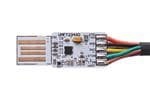
| 描述 | BRD BRKOUT USB FT234XD WIRE END界面开发工具 USB to UART w/4 Cntl Bus, 6" Flying Leads |
| 产品分类 | |
| 品牌 | FTDI |
| 产品手册 | |
| 产品图片 |
|
| rohs | 符合RoHS无铅 / 符合限制有害物质指令(RoHS)规范要求 |
| 产品系列 | 模拟与数字IC开发工具,界面开发工具,FTDI UMFT234XD-WEUSBmadeEZ-UART |
| 数据手册 | |
| 产品型号 | UMFT234XD-WE |
| 主要属性 | 全速(12Mbps),经由连接到 PCB 的 8 个 6" 引线的 UART 信号 |
| 主要用途 | 接口,USB 2.0 至 UART |
| 产品 | Development Modules |
| 产品种类 | 界面开发工具 |
| 使用的IC/零件 | FT234XD |
| 其它名称 | 768-1175 |
| 参考设计库 | http://www.digikey.com/rdl/4294959866/4294959865/1099 |
| 商标 | FTDI |
| 封装 | Bulk |
| 尺寸 | 36.3 mm x 12.1 mm x 2 mm |
| 嵌入式 | 是,ASIC |
| 工作电源电压 | 3.3 V |
| 工作电源电流 | 50 mA |
| 工具用于评估 | FT234XD |
| 工厂包装数量 | 5 |
| 所含物品 | 板 |
| 接口类型 | UART, USB |
| 标准包装 | 5 |
| 特色产品 | http://www.digikey.cn/product-highlights/cn/zh/ftdi-umft234xd-modules/3390 |
| 用于 | FT234XD |
| 类型 | USB to UART |
| 辅助属性 | USB 充电检测 |

/MFG_UMFT234XD-WE.jpg)


- 商务部:美国ITC正式对集成电路等产品启动337调查
- 曝三星4nm工艺存在良率问题 高通将骁龙8 Gen1或转产台积电
- 太阳诱电将投资9.5亿元在常州建新厂生产MLCC 预计2023年完工
- 英特尔发布欧洲新工厂建设计划 深化IDM 2.0 战略
- 台积电先进制程称霸业界 有大客户加持明年业绩稳了
- 达到5530亿美元!SIA预计今年全球半导体销售额将创下新高
- 英特尔拟将自动驾驶子公司Mobileye上市 估值或超500亿美元
- 三星加码芯片和SET,合并消费电子和移动部门,撤换高东真等 CEO
- 三星电子宣布重大人事变动 还合并消费电子和移动部门
- 海关总署:前11个月进口集成电路产品价值2.52万亿元 增长14.8%


PDF Datasheet 数据手册内容提取
UMFT234XD Datash eet Version 1.1 Document Reference No.: FT_000801 Clearance No.: FTDI# 327 Future Technology Devices International Datasheet UMFT234XD Breakout Modules UMFT234XD is a USB to UART breakout module Introduction 1 The UMFT234XD breakout module utilizes FTDI’s FT234XD IC to convert USB to UART. 1.1 Features The UMFT234XD is a breakout board that converts USB2.0 Full-Speed to UART. These modules do not have a USB connector, instead, the modules plug directly into the USB host connector and the pads of the PCB makes electrical contact with the electrical contacts of the USB connector. The UART interface operates at +3.3V voltage levels, however all I/Os are 5V tolerant. 1.2 Ordering Information Module Interface Features UMFT234XD-01 UART USB to UART with four control bus lines, 3.3V power out limited to 50mA and 5V with as safety fuse. UART signals available via 8 pin female connector. UMFT234XD-NC UART USB to UART with four control bus lines, 3.3V power out limited to 50mA and 5V with as safety fuse. UART signals available via 8 pads on the PCB. UMFT234XD-WE UART USB to UART with four control bus lines, 3.3V power out limited to 50mA and 5V with as safety fuse. UART signals available via 8, 6” flying leads connected to the PCB pads. Driver Support 2 Royalty-Free VIRTUAL COM PORT (VCP): Royalty-Free D2XX Direct Drivers: Windows 8 32,64-bit Windows 8 32,64-bit Windows 7 32,64-bit Windows 7 32,64-bit Windows Vista Windows Vista Windows XP 32,64-bit Windows XP 32,64-bit Windows XP Embedded Windows XP Embedded Windows CE.NET 4.2 , 5.0 and 6.0 Windows CE.NET 4.2, 5.0 and 6.0 MAC OS OS-X MAC OS OS-X Linux 3.0 and greater Linux 3.0 and greater Android Android The drivers listed above are all available to download for free from www.ftdichip.com. Various 3rd Party Drivers are also available for various other operating systems - visit www.ftdichip.com for details. Use of FTDI devices in life support and/or safety applications is entirely at the user’s risk, and the user agrees to defend, indemnify and hold harmless FTDI from any and all damages, claims, suits or expense resulting from such use.
UMFT234XD Datasheet Version 1.1 Document Reference No.: FT_000801 Clearance No.: FTDI# 327 Table of Contents 1 Introduction ................................................................................... 1 1.1 Features ........................................................................................................ 1 1.2 Ordering Information .................................................................................... 1 2 Driver Support ................................................................................ 1 3 UMFT234XD Signals and Configurations ......................................... 3 3.1 UMFT234XD CN1 Signal Descriptions ............................................................ 3 3.2 UMFT234XD CN2 Signal Descriptions ............................................................ 3 3.3 CBUS Signal Options ..................................................................................... 4 3.4 Configuring the MTP ROM .............................................................................. 5 4 Module Dimensions ........................................................................ 5 5 Module Wire Connections ............................................................... 6 5.1 UMFT234XD-WE Wire Connections ................................................................ 6 5.2 UMFT234XD-WE ............................................................................................ 6 6 Module Circuit Schematic ............................................................... 7 6.1 UMFT234XD Schematic ................................................................................. 7 7 Environmental Compliances ........................................................... 7 8 Internal MTP ROM Configuration .................................................... 8 9 Contact Information ....................................................................... 9 Appendix A - List of Figures and Tables ................................................................... 9 Appendix B: Revision History ................................................................................ 10 2 Copyright © 2015 Future Technology Devices International Limited
UMFT234XD Datasheet Version 1.1 Document Reference No.: FT_000801 Clearance No.: FTDI# 327 UMFT234XD Signals and Configurations 3 CN1 connects directly to a USB host or HUB port, or can be connected to a USB extension cable. This connects to USB signals, 5V USB Bus power and GND. When connecting the module to a USB host or HUB the signal pads should be facing upwards when connecting to a horizontal connector and be facing right for vertical connectors. If the module is plugged in upside down no connectivity will be made between PCB and HUB, no damage will occur from plugging the module in the wrong way. 3.1 UMFT234XD CN1 Signal Descriptions Pin No. Name Type Description 5V Power input USB port. For a low power USB bus powered design, up to 100mA can 1 VBUS PWR be sourced from the 5V supply on the USB bus. A maximum of 500mA can be sourced from the USB bus in a high power USB bus powered design. 2 D- Signal Negative USB data signal 3 D+ Signal Positive USB data signal 4 GND PWR Module Ground Table 3.1 USB Connector Pin Out Description 3.2 UMFT234XD CN2 Signal Descriptions Pin No. Name Type Description 1 TXD Output UART transmit data PWR 2 VBUS 5V Power output USB port. Output 3 GND PWR Module Ground Supply 4 RESET# Input Can be used by an external device to reset the FT234XD. 5 RXD Input UART receive data 3.3V output from FT234XD integrated LDO regulator. This pin is decoupled to ground 6 3V3 Output on the module PCB with a 10nF capacitor and offers 3V3 at up to 50mA for external hardware. 7 RTS# Output UART Ready to Send handshake signal 8 GND PWR Module Ground Supply 9 CTS# Input UART Clear to Send handshake signal Configurable CBUS0 I/O Pin. The function of this pin is configured in the device internal 10 CB0 I/O MTP ROM. See Table 3.3 Table 3.2 UART Module Pin Out Description 3 Copyright © 2015 Future Technology Devices International Limited
UMFT234XD Datasheet Version 1.1 Document Reference No.: FT_000801 Clearance No.: FTDI# 327 3.3 CBUS Signal Options CBUS Signal Available On Description Option CBUS Pin Tristate CBUS0 IO Pad is tri-stated DRIVE_1 CBUS0 Output a constant 1 DRIVE_0 CBUS0 Output a constant 0 TXDEN CBUS0 Enable transmit data for RS485 Output is low after the device has been configured by USB, then high during PWREN# CBUS0 USB suspend mode. This output can be used to control power to external logic. Transmit data LED drive – open drain pulses low when transmitting data via TXLED# CBUS0 UART. RXLED# CBUS0 Receive data LED drive – open drain pulses low when receiving data via UART. LED drive – open drain pulses low when transmitting or receiving data via TX&RXLED# CBUS0 UART. Goes low during USB suspend mode. Typically used to power down external SLEEP# CBUS0 logic to RS232 level converter IC in USB to RS232 converter designs CLK24MHz CBUS0 24 MHz Clock output.** CLK12MHz CBUS0 12 MHz Clock output.** CLK6MHz CBUS0 6 MHz Clock output.** CBUS bit bang mode option. Allows up to 4 of the CBUS pins to be used as general purpose I/O. A separate application note, AN232R-01, available from GPIO CBUS0 FTDI website (www.ftdichip.com) describes in more detail how to use CBUS bit bang mode. Battery Charge Detect indicates when the device is connected to a dedicated BCD_Charger CBUS0 battery charger host. Active high output. NOTE: Requires a 10K pull-down to remove power up toggling. Active low BCD Charger, driven by an open drain to ground with no internal BCD_Charger# CBUS0 pull-up. BitBang_WR# CBUS0 Synchronous and asynchronous bit bang mode WR# strobe output. BitBang_RD# CBUS0 Synchronous and asynchronous bit bang mode RD# strobe output. VBUS_Sense CBUS0 Input to detect when VBUS is present. Time_Stamp CBUS0 Toggle signal which changes state each time a USB SOF is received Keep_Awake# CBUS0 Active Low input, prevents the chip from going into suspend. Table 3.3 CBUS Configuration Control * PWREN# must be used with a 10kΩ resistor pull up. **When in USB suspend mode the outputs clocks are also suspended. 4 Copyright © 2015 Future Technology Devices International Limited
UMFT234XD Datasheet Version 1.1 Document Reference No.: FT_000801 Clearance No.: FTDI# 327 3.4 Configuring the MTP ROM The FT234XD IC on the module contains an embedded MTP ROM, this can be used to specify the functions of the CBUS0 pin, the current drive on each signal pin, current limit for the USB bus and the descriptors of the device. These features can be programmed using FTDI’s programming utility FT_Prog. For details on using FT_Prog, please see the FT_PROG User Guide. When programming the MTP ROM please note: i) The Max Bus Power setting of the MTP ROM should specify the maximum current to be drawn from the USB host/hub when enumerated. For high-powered USB devices the current limit when enumerated is between 100mA and 500mA, for low-powered USB devices the current limit is 100mA. Module Dimensions 4 36.3 15.5 14.1 0 4 1 5 9 2. 2. 4. 1 1 4 2. 44.5 2.00 Measurements given in millimetres Tolerance +/-0.1mm Figure 4.1 UMFT234XD-01 Module Dimensions 5 Copyright © 2015 Future Technology Devices International Limited
UMFT234XD Datasheet Version 1.1 Document Reference No.: FT_000801 Clearance No.: FTDI# 327 Module Wire Connections 5 5.1 UMFT234XD-WE Wire Connections 2 VBUS 2 RED 1 TXD 1 ORANGE RXD 5 5 YELLOW RTS# 7 7 GREEN CTS# 9 Wire 6" 9 BROWN GND 8 8 GREY CB0 10 10 PURPLE RESET# 4 4 WHITE 6 3v3 6 BLUE 3 GND 3 BLACK Figure 5.1 UMFT234XD-WE Wire Connections (numbers refer to pad numbers on the PCB) Figure 5.1 illustrates the –WE product as a cable. This is only for illustration purposes. The wire ended product consists of individual wires – not a cable 5.2 UMFT234XD-WE Figure 5.2 UMFT234XD-WE Image 6 Copyright © 2015 Future Technology Devices International Limited
UMFT234XD Datasheet Version 1.1 Document Reference No.: FT_000801 Clearance No.: FTDI# 327 Module Circuit Schematic 6 6.1 UMFT234XD Schematic Figure 6.1 UMFT234XD Circuit Schematic Environmental Compliances 7 The UMFT234XD modules exclusively use lead free components, and are fully compliant with European Union directive 2002/95/EC. 7 Copyright © 2015 Future Technology Devices International Limited
UMFT234XD Datasheet Version 1.1 Document Reference No.: FT_000801 Clearance No.: FTDI# 327 Internal MTP ROM Configuration 8 Following a power-on reset or a USB reset the FT234XD will scan its internal MTP ROM and read the USB configuration descriptors stored there. The default values programmed into the internal MTP ROM in the FT234XD used on the UMFT234XD are shown in Table 8.1. Parameter Value Notes USB Vendor ID (VID) 0403h FTDI default VID (hex) USB Product UD (PID) 6015h FTDI default PID (hex) Serial Number Enabled? Yes A unique serial number is generated and programmed into Serial Number See Note the MTP ROM during final test of the UMFT234XD module. Enabling this option will make the device pull down on the Pull down I/O Pins in USB Disabled UART interface lines when the power is shut off (PWREN# Suspend is high). Manufacturer Name FTDI Product Description UMFT234XD Max Bus Power Current 90mA Power Source Bus Powered Device Type FT234XD Returns USB 2.0 device description to the host. Note: The USB Version 0200 device is a USB 2.0 Full Speed device (12Mb/s). Taking RI# low will wake up the USB host controller from Remote Wake Up Enabled suspend. Enables the high drive level on the serial and CBUS I/O High Current I/Os Disabled pins. Makes the device load the VCP driver interface for the Load VCP Driver Enabled device. CBUS0 PWREN# Table 8.1 Default Internal MTP ROM Configuration The internal MTP ROM in the FT234XD can be programmed over USB using the utility program FT_PROG. FT_PROG can be downloaded from www.ftdichip.com. Users who do not have their own USB vendor ID but who would like to use a unique Product ID in their design can apply to FTDI for a free block of unique PIDs. Contact FTDI Support (support1@ftdichip.com) for this service. 8 Copyright © 2015 Future Technology Devices International Limited
UMFT234XD Datasheet Version 1.1 Document Reference No.: FT_000801 Clearance No.: FTDI# 327 Contact Information 9 Head Office – Glasgow, UK Branch Office – Hillsboro, Oregon, USA Future Technology Devices International Limited 7130 SW Fir Loop Unit 1, 2 Seaward Place, Centurion Business Park Tigard, OR 97223-8160 Glasgow G41 1HH USA United Kingdom Tel: +1 (503) 547 0988 Tel: +44 (0) 141 429 2777 Fax: +1 (503) 547 0987 Fax: +44 (0) 141 429 2758 E-Mail (Sales) us.sales@ftdichip.com E-mail (Sales) sales1@ftdichip.com E-Mail (Support) us.support@ftdichip.com E-mail (Support) support1@ftdichip.com E-Mail (General Enquiries) us.admin@ftdichip.com E-mail (General Enquiries) admin1@ftdichip.com Branch Office – Shanghai, China Branch Office – Taipei, Taiwan Room 1103, No. 666 West Huaihai Road, 2F, No. 516, Sec. 1, NeiHu Road Shanghai, 200052 Taipei 114 China Taiwan , R.O.C. Tel: +86 (0)21 6235 1596 Tel: +886 (0) 2 8791 3570 Fax: +86 (0)21 6235 1595 Fax: +886 (0) 2 8791 3576 E-mail (Sales) cn.sales@ftdichip.com E-mail (Sales) tw.sales1@ftdichip.com E-mail (Support) cn.support@ftdichip.com E-mail (Support) tw.support1@ftdichip.com E-mail (General Enquiries) cn.admin@ftdichip.com E-mail (General Enquiries) tw.admin1@ftdichip.com Web Site http://ftdichip.com Distributor and Sales Representatives Please visit the Sales Network page of the FTDI Web site for the contact details of our distributor(s) and sales representative(s) in your country. System and equipment manufacturers and designers are responsible to ensure that their systems, and any Future Technology Devices International Ltd (FTDI) devices incorporated in their systems, meet all applicable safety, regulatory and system-level performance requirements. All application-related information in this document (including application descriptions, suggested FTDI devices and other materials) is provided for reference only. While FTDI has taken care to assure it is accurate, this information is subject to customer confirmation, and FTDI disclaims all liability for system designs and for any applications assistance provided by FTDI. Use of FTDI devices in life support and/or safety applications is entirely at the user’s risk, and the user agrees to defend, indemnify and hold harmless FTDI from any and all damages, claims, suits or expense resulting from such use. This document is subject to change without notice. No freedom to use patents or other intellectual property rights is implied by the publication of this document. Neither the whole nor any part of the information contained in, or the product described in this document, may be adapted or reproduced in any material or electronic form without the prior written consent of the copyright holder. Future Technology Devices International Ltd, Unit 1, 2 Seaward Place, Centurion Business Park, Glasgow G41 1HH, United Kingdom. Scotland Registered Company Number: SC136640 9 Copyright © 2015 Future Technology Devices International Limited
UMFT234XD Datasheet Version 1.1 Document Reference No.: FT_000801 Clearance No.: FTDI# 327 Appendix A - List of Figures and Tables List of Figures Figure 4.1 UMFT234XD-01 Module Dimensions ........................................................................................... 5 Figure 5.1 UMFT234XD-WE Wire Connections (numbers refer to pad numbers on the PCB) ................ 6 Figure 5.2 UMFT234XD-WE Image ................................................................................................................. 6 Figure 6.1 UMFT234XD Circuit Schematic .................................................................................................... 7 List of Tables Table 3.1 USB Connector Pin Out Description ............................................................................................. 3 Table 3.2 UART Module Pin Out Description ................................................................................................ 3 Table 3.3 CBUS Configuration Control .......................................................................................................... 4 Table 8.1 Default Internal MTP ROM Configuration ..................................................................................... 8 Copyright © 2013 Future Technology Devices International Limited 9
UMFT234XD Datasheet Version 1.1 Document Reference No.: FT_000801 Clearance No.: FTDI# 327 Appendix B: Revision History Document Title: UMFT234XD Document Reference No.: FT_000801 Clearance No.: FTDI# 327 Product Page: http://www.ftdichip.com/FT-X.htm Document Feedback: Send Feedback Version 1.0 Initial Datasheet Created 31/01/13 Version 1.1 Corrected -01 part number 06/07/15 Copyright © 2013 Future Technology Devices International Limited 10
Mouser Electronics Authorized Distributor Click to View Pricing, Inventory, Delivery & Lifecycle Information: F TDI: UMFT234XD-WE UMFT234XD-NC UMFT234XD-01