ICGOO在线商城 > 集成电路(IC) > PMIC - 电源管理 - 专用 > UCD9240PFC
 Datasheet下载
- 型号: UCD9240PFC
- 制造商: Texas Instruments
- 库位|库存: xxxx|xxxx
- 要求:
| 数量阶梯 | 香港交货 | 国内含税 |
| +xxxx | $xxxx | ¥xxxx |
查看当月历史价格
查看今年历史价格
UCD9240PFC产品简介:
ICGOO电子元器件商城为您提供UCD9240PFC由Texas Instruments设计生产,在icgoo商城现货销售,并且可以通过原厂、代理商等渠道进行代购。 UCD9240PFC价格参考¥65.49-¥85.62。Texas InstrumentsUCD9240PFC封装/规格:PMIC - 电源管理 - 专用, Special Purpose PMIC 80-TQFP (12x12)。您可以下载UCD9240PFC参考资料、Datasheet数据手册功能说明书,资料中有UCD9240PFC 详细功能的应用电路图电压和使用方法及教程。
UCD9240PFC 是由 Texas Instruments(德州仪器)生产的一款专用电源管理集成电路 (PMIC),主要应用于需要高效、高精度电压和电流控制的场景。该器件专为多相降压转换器设计,能够实现对多个电源轨的精确管理和监控。

 应用场景

1. 服务器和数据中心:
   UCD9240PFC 在服务器和数据中心中广泛用于为处理器(如 CPU 和 GPU)提供稳定的电源。这些应用场景要求电源系统具备高效率、低噪声和快速响应特性,以应对瞬态负载变化。UCD9240PFC 支持多相操作,可以有效降低纹波电压,提高系统的稳定性和可靠性。

2. 通信基础设施:
   在通信设备中,如基站、路由器和交换机,UCD9240PFC 用于为高性能 FPGA、ASIC 和网络处理器供电。这些设备通常需要多个电源轨,并且对电源的精度和响应速度有严格要求。UCD9240PFC 可以通过其灵活的配置选项和内置的故障保护功能,确保电源系统的稳定运行。

3. 工业自动化:
   工业控制系统中的可编程逻辑控制器 (PLC) 和运动控制器等设备也依赖于 UCD9240PFC 来提供可靠的电源管理。这些设备通常工作在恶劣的环境条件下,因此对电源的可靠性和稳定性要求极高。UCD9240PFC 的高集成度和强大的保护功能使其成为工业应用的理想选择。

4. 消费电子:
   在高端消费电子产品中,如游戏主机和高性能笔记本电脑,UCD9240PFC 用于为图形处理单元 (GPU) 和其他关键组件供电。这些产品需要高效的电源管理来延长电池寿命并提高性能表现。UCD9240PFC 的多相架构可以有效分散热量,提高系统的散热效率。

5. 汽车电子:
   在电动汽车和自动驾驶系统中,UCD9240PFC 用于为车载计算机和传感器供电。这些应用场景要求电源系统具备高度的可靠性和抗干扰能力,以确保车辆的安全性和稳定性。UCD9240PFC 的宽输入电压范围和强大的保护机制使其能够在复杂的汽车环境中稳定工作。

总之,UCD9240PFC 凭借其卓越的性能和灵活性,适用于多种需要高效、高精度电源管理的应用场景,特别是在对电源质量和可靠性有严格要求的领域。
| 参数 | 数值 |
| 产品目录 | 集成电路 (IC)半导体 |
| 描述 | IC DGTL PWM SYSTEM CTRLR 80-TQFP开关控制器 Dig Pwr Pt of Load Sys Cntrlr |
| 产品分类 | |
| 品牌 | Texas Instruments |
| 产品手册 | |
| 产品图片 |
|
| rohs | 符合RoHS无铅 / 符合限制有害物质指令(RoHS)规范要求 |
| 产品系列 | 电源管理 IC,开关控制器 ,Texas Instruments UCD9240PFCFusion Digital Power™ |
| 数据手册 | |
| 产品型号 | UCD9240PFC |
| 产品目录页面 | |
| 产品种类 | 开关控制器 |
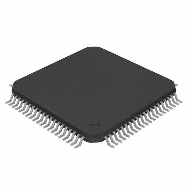
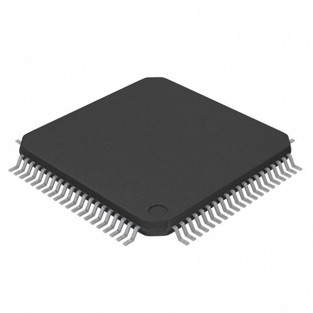
| 供应商器件封装 | 80-TQFP(12x12) |
| 其它名称 | 296-23690 |
| 包装 | 托盘 |
| 单位重量 | 373.600 mg |
| 占空比-最大 | 100 % |
| 商标 | Texas Instruments |
| 安装类型 | 表面贴装 |
| 安装风格 | SMD/SMT |
| 封装 | Tray |
| 封装/外壳 | 80-TQFP |
| 封装/箱体 | TQFP-80 |
| 工作温度 | -40°C ~ 110°C |
| 工作电源电压 | 3 V to 3.6 V |
| 工作电源电流 | 55 mA |
| 工厂包装数量 | 96 |
| 应用 | |
| 开关频率 | 2 MHz |
| 拓扑结构 | Buck |
| 描述/功能 | DIGITAL POINT OF LOAD SYSTEM CONTROLLER |
| 最大工作温度 | + 125 C |
| 最小工作温度 | - 40 C |
| 标准包装 | 96 |
| 电压-电源 | 3 V ~ 3.6 V |
| 电流-电源 | - |
| 类型 | Voltage Mode PWM Controllers |
| 系列 | UCD9240 |
| 输出电流 | 6 mA |
| 输出端数量 | 8 Output |


- 商务部:美国ITC正式对集成电路等产品启动337调查
- 曝三星4nm工艺存在良率问题 高通将骁龙8 Gen1或转产台积电
- 太阳诱电将投资9.5亿元在常州建新厂生产MLCC 预计2023年完工
- 英特尔发布欧洲新工厂建设计划 深化IDM 2.0 战略
- 台积电先进制程称霸业界 有大客户加持明年业绩稳了
- 达到5530亿美元!SIA预计今年全球半导体销售额将创下新高
- 英特尔拟将自动驾驶子公司Mobileye上市 估值或超500亿美元
- 三星加码芯片和SET,合并消费电子和移动部门,撤换高东真等 CEO
- 三星电子宣布重大人事变动 还合并消费电子和移动部门
- 海关总署:前11个月进口集成电路产品价值2.52万亿元 增长14.8%


PDF Datasheet 数据手册内容提取
UCD9240 www.ti.com................................................................................................................................................... SLUS766C–JULY2008–REVISEDNOVEMBER2008 Digital PWM System Controller FEATURES • SupportedbyFusionDigitalPower™ 1 • FullyConfigurableMulti-Outputand Designer,aFullFeaturedPCBasedDesign 2 Multi-PhaseNon-IsolatedDC/DCPWM TooltoSimulate,Configure,andMonitor Controller PowerSupplyPerformance. • ControlsUpToFourVoltageRailsandUpTo APPLICATIONS EightPhases • Industrial/ATE • SupportsSwitchingFrequenciesUpto2MHz • NetworkingEquipment With250psDuty-CycleResolution • TelecommunicationsEquipment • UpTo1mVClosedLoopResolution • Servers • Hardware-Accelerated,3-Pole/3-Zero • StorageSystems CompensatorWithNon-LinearGainfor • FPGA,DSPandMemoryPower ImprovedTransientPerformance • SupportsMultipleSoft-StartandSoft-Stop DESCRIPTION ConfigurationsIncludingPrebiasStart-up • SupportsVoltageTracking,Marginingand The UCD9240 is a multi-rail, multi-phase synchronousbuckdigitalPWMcontroller designed for Sequencing non-isolated DC/DC power applications. This device • SupportsCurrentandTemperatureBalancing integrates dedicated circuitry for DC/DC loop forMulti-PhasePowerStages management with flash memory and a serial interface • SupportsPhaseAdding/Sheddingfor to support configurability, monitoring and Multi-PhasePowerStages management. • SyncIn/OutPinsAlignDPWMClocks The UCD9240 was designed to provide a wide BetweenMultipleUCD9240Devices variety of desirable features for non-isolated DC/DC • FanMonitoringandControl converter applications while minimizing the total system component count by reducing external • 12-BitDigitalMonitoringofPowerSupply circuits. The solution integrates multi-loop ParametersIncluding: management with sequencing, margining, tracking – InputCurrentandVoltage and intelligent phase management to optimize for total system efficiency. Additionally, loop – OutputCurrentandVoltage compensation and calibration are supported without – TemperatureatEachPowerStage theneedtoaddexternalcomponents. • MultipleLevelsofOvercurrentFault To facilitate configuring the device, the Texas Protection: Instruments Fusion Digital Power™ Designer is – ExternalCurrentFaultInputs provided. This PC based Graphical User Interface – AnalogComparatorsMonitorCurrent offers an intuitive interface to the device. This tool SenseVoltage allows the design engineer to configure the system operating parameters for the application, store the – CurrentContinuallyDigitallyMonitored configuration to on-chip non-volatile memory and • OverandUndervoltageFaultProtection observe both frequency domain and time domain • OvertemperatureFaultProtection simulationsforeachofthepowerstageoutputs. • EnhancedNonvolatileMemoryWithError TI has also developed multiple complementary power CorrectionCode(ECC) stage solutions – from discrete drives in the UCD7k • DeviceOperatesFromaSingleSupplyWithan family to fully tested power train modules in the PTD family. These solutions have been developed to InternalRegulatorControllerThatAllows complement the UCD9k family of system power OperationOveraWideSupplyVoltageRange controllers. 1 Pleasebeawarethatanimportantnoticeconcerningavailability,standardwarranty,anduseincriticalapplicationsofTexas Instrumentssemiconductorproductsanddisclaimerstheretoappearsattheendofthisdatasheet. FusionDigitalPower,Auto-IDaretrademarksofTexasInstruments. 2 PRODUCTIONDATAinformationiscurrentasofpublicationdate. Copyright©2008,TexasInstrumentsIncorporated Products conform to specifications per the terms of the Texas Instruments standard warranty. Production processing does not necessarilyincludetestingofallparameters.
UCD9240 SLUS766C–JULY2008–REVISEDNOVEMBER2008................................................................................................................................................... www.ti.com Thesedeviceshavelimitedbuilt-inESDprotection.Theleadsshouldbeshortedtogetherorthedeviceplacedinconductivefoam duringstorageorhandlingtopreventelectrostaticdamagetotheMOSgates. ORDERINGINFORMATION(1) OPERATING ORDERABLEPART TOPSIDE TEMPERATURE PINCOUNT SUPPLY PACKAGE NUMBER MARKING RANGE,T A UCD9240PFCR 80-pin Reelof1000 QFP UCD9240 UCD9240PFC 80-pin Trayof119 QFP UCD9240 -40°Cto110°C UCD9240RGCR 64-pin Reelof2000 QFN UCD9240 UCD9240RGCT 64-pin Reelof250 QFN UCD9240 (1) Forthemostcurrentpackageandorderinginformation,seethePackageOptionAddendumattheendofthisdocument,orseetheTI websiteatwww.ti.com. ELECTRICAL SPECIFICATIONS ABSOLUTE MAXIMUM RATINGS(1) VALUE UNIT VoltageappliedatV33DtoDV –0.3to3.8 V SS VoltageappliedatV33AtoAV –0.3to3.8 V SS Voltageappliedtoanypin (2) –0.3to3.8 V Storagetemperature(T ) –40to150 °C STG (1) Stressesbeyondthoselistedunderabsolutemaximumratingsmaycausepermanentdamagetothedevice.Thesearestressratings onlyandfunctionaloperationofthedeviceattheseoranyotherconditionsbeyondthoseindicatedunderrecommendedoperating conditionsisnotimplied.Exposuretoabsolute-maximum-ratedconditionsforextendedperiodsmayaffectdevicereliability. (2) AllvoltagesreferencedtoV . SS RECOMMENDED OPERATING CONDITIONS Overoperatingfree-airtemperaturerange(unlessotherwisenoted). MIN NOM MAX UNIT V Supplyvoltageduringoperation,V33D,V33DIO,V33A 3 3.3 3.6 V T Operatingfree-airtemperaturerange –40 110 °C A T Junctiontemperature 125 °C J 2 SubmitDocumentationFeedback Copyright©2008,TexasInstrumentsIncorporated ProductFolderLink(s):UCD9240
UCD9240 www.ti.com................................................................................................................................................... SLUS766C–JULY2008–REVISEDNOVEMBER2008 ELECTRICAL CHARACTERISTICS PARAMETER TESTCONDITIONS MIN NOM MAX UNIT SUPPLYCURRENT I V =3.3V 8 15 V33A V33A I V =3.3V 2 10 V33DIO V33DIO I Supplycurrent V =3.3V 40 45 mA V33D V33D V =3.3Vstoringconfiguration I V33D 50 55 V33D parametersinflashmemoryTBD INTERNALREGULATORCONTROLLERINPUTS/OUTPUTS V 3.3-Vlinearregulator EmitterofNPNtransistor 3.25 3.3 3.35 V33 V V33FB 3.3-Vlinearregulatorfeedback 4 4.6 I Seriespassbasedrive V =12V 10 mA V33FB VIN Beta SeriesNPNpassdevice 40 EXTERNALLYSUPPLIED3.3VPOWER V , V33D Digital3.3-Vpower T 3.13 3.47 V V A=25°C V33DION V Analog3.3-Vpower T 3.13 3.47 V V33A A=25°C ERRORAMPLIFIERINPUTSEAPn,EANn V Commonmodevoltageeachpin -0.15 1.848 V CM V DifferentialVoltageRange -0.256 1.998 V DIFF V InternalerrorVoltagerange AFE_GAINfieldofCLA_GAINS=0(1) -256 248 mV ERROR EAP-EAN Errorvoltagedigitalresolution AFE_GAINfieldofCLA_Gains=3 1 mV R InputImpedance Groundreference 0.5 1.5 3 MΩ EA I Inputoffsetcurrent 1kΩsourceimpedence -5 5 m A OFFSET ANALOGINPUTSCS,V ,TEMP,PMBusADDR in I BiascurrentforPMBusAddrpins 9 11 m A BIAS V Voltageindicatingopenpin AddrSens0,1open 2.47 V ADDR_OPEN V Voltageindicatingshortedpin AddrSense0,1shorttoground 0.179 V ADDR_SHORT Inputs:V ,V ,V Measurmentrangeforvoltage In track temp V CS-1A,CS-1B,CS-2A,CS-2B 0 2.5 V ADC_RANGE monitoring CS-3A,CS-3B,CS-4A,CS-4B Overcurrentcomparatorthreshold V Inputs:CS-1A,CS-2A,CS-3A,CS-4A 0.032 2 V OC_THRS voltagerange Overcurrentcomparatorthreshold V Inputs:CS-1A,CS-2A,CS-3A,CS-4A 31.25 mV OC_RES voltagerange ADCREF ExternalReferenceinput (80-pinpackage) 1.8 V33A V Temp Int.temperaturesenseaccuracy Overrangefrom0°Cto100°C -5 5 °C internal INL ADCintegralnonlinearity -2.5 2.5 mV I Inputleakagecurrent 3Vappliedtopin 100 nA lkg R Inputimpedance Groundreference 8 MΩ IN C CurrentSenseInputcapacitance 10 pF IN (1) SeetheUCD92xxPMBusCommandReferenceforthedescriptionoftheAFE_GAINfieldofCLA_GAINScommand. Copyright©2008,TexasInstrumentsIncorporated SubmitDocumentationFeedback 3 ProductFolderLink(s):UCD9240
UCD9240 SLUS766C–JULY2008–REVISEDNOVEMBER2008................................................................................................................................................... www.ti.com ELECTRICAL CHARACTERISTICS (continued) PARAMETER TESTCONDITIONS MIN NOM MAX UNIT DIGITALINPUTS/OUTPUTS Dgnd V Low-leveloutputvoltage I =6mA(2),V =3V V OL OL V33DIO +0.25 V V High-leveloutputvoltage I =-6mA(3),V =3V 33DIO V OH OH V33DIO -0.6V V High-levelinputvoltage V =3V 2.1 3.6 V IH V33DIO V Low-levelinputvoltage V =3.5V 1.1 V IL V33DIO FANCONTROLINPUTS/OUTPUTS T FAN-PWMperiod 156 kHz PWM_PERIOD DUTY FAN-PWMdutycyclerange 0% 100% PWM DUTY Dutycycleresolution 1% RES For1Tachpulseperrevolution.At2, Tach FAN-TACHrange 30 300k RPM RANGE 3,or4pulse/rev,dividebythatvalue Tach FAN-TACHresolution For1Tachpulseperrevolution 30 RPM RES t FAN-TACHminimumpulsewidth Eitherpositiveornegativepolarity 150 m s MIN SYSTEMPERFORMANCE V commandedtobe1V,at25°C ref VRef SetpointReferenceAccuracy AFEgain=4,1VinputtoEAP/N -10 10 mV measuredatoutputoftheEADC(4) SetpointReferenceAccuracyover -40°Cto125°C -20 20 mV temeprature Differentialoffsetbetweengain AFEgain=4comparedto V -4 4 mV DiffOffset setetings AFEgain=1,2,or8 t DigitalCompensatorDelay(5) 208(6) ns Delay F SwitchingFrequency 15.260 2000 kHz SW Duty MaxandMinDutyCycle ConfiguredviaPMBus 0% 100% V Slew MinimumV slewrate V slewratebetween2.3Vand2.9V 0.25 V/ms DD DD DD t Retentionofconfigurationparameters T =25°C 100 Years retention J Numberofnonvolatileerase/write Write_Cycles T =25°C 20 Kcycles cycles J (2) ThemaximumI ,foralloutputscombined,shouldnotexceed12mAtoholdthemaximumvoltagedropspecified. OL (3) ThemaximumI ,foralloutputscombined,shouldnotexceed48mAtoholdthemaximumvoltagedropspecified. OH (4) Withdefaultdevicecaliibration.PMBuscalibrationcanbeusedtoimprovetheregulationtolerance. (5) TimefromcloseoferrorADCsamplewindowtotimewhendigitallycalculatedcontroleffort(dutycycle)isavailable.Thisdelaymustbe accountedforwhencalculatingthesystemdynamicresponse. (6) ThePMBuscommand:EADC_SAMPLE_TRIGGERdefinesthestartofthe32nsADCsamplewindow.Sotheminimum EAD_SAMPLE_TRIGGERtimeis208+32=240ns. 4 SubmitDocumentationFeedback Copyright©2008,TexasInstrumentsIncorporated ProductFolderLink(s):UCD9240
UCD9240 www.ti.com................................................................................................................................................... SLUS766C–JULY2008–REVISEDNOVEMBER2008 ADC MONITORING INTERVALS AND RESPONSE TIMES The ADC operates in a continuous conversion sequence that measures each rail's output voltage, each power stage's ouput current, plus four other variables (external temperature, Internal temperature, input voltage and current, and tracking input voltage). The length of the sequence is determined by the number of output rails (NumRails) and total output power stages (NumPhases) configured for use. The time to complete the monitoring samplingsequenceisgivebytheformula: t =t ×(NumRAILS+NumPHASE+4) ADC_SEQ ADC PARAMETER TESTCONDITIONS MIN TYP MAX UNIT t ADCsingle-sampletime 3.84 m s ADC Min=1Rail+1Phase+4=6 samples t ADCsequencerinterval 23.04 61.44 m s ADC_SEQ Max=4Rails+8Phases+4=16 samples The most recent ADC conversion results are periodically converted into the proper measurement units (volts, amperes, degrees), and each measurement is compared to its corresponding fault and warning limits. The monitoringoperatesasynchronouslytotheADC,atintervalsshowninthetablebelow. PARAMETER TESTCONDITIONS MIN TYP MAX UNIT t Outputvoltagemonitoringinterval 200 m s Vout 200× t Outputcurrentmonitoringinterval m s Iout N Rails t Inputvoltagemonitoringinterval 2 ms Vin t Inputcurrentmonitoringinterval 2 ms Iin t Temepraturemonitoringinterval 800 ms TEMP t Outputcurrentbalancinginterval 2 ms Ibal t Fanspeedmonitoringinterval 1000 ms FanTach Because the ADC sequencer and the monitoring comparisons are asynchronous to each other, the response time to a fault condition depends on where the event occurs within the monitoring interval and within the ADC sequence interval. Once a fault condition is detected, some additional time is required to determine the correct action based on the FAULT_RESPONSE code, and then to perform the appropriate response. The following tableliststheworse-casefaultresponsetimes. PARAMETER TESTCONDITIONS MAXTIME UNIT t ,t Over/undervoltagefaultresponsetimeduring Normalregulation,noPMBusactivity, 300 m s OVF UVF normaloperation 8stagesenabled tOVF,tUVF Olovgegrin/ugndervoltagefaultresponsetime,duringdata Dmuerminogryd(a1t)aloggingtononvolatile 800 m s t ,t Over/undervoltagefaultresponsetime,when Duringtrackingandsoft-startramp. 400 m s OVF UVF trackingorsequencingenable t ,t Over/undercurrentfaultresponsetimeduring N8osrtmagaelsreegnualabtleiodn,noPMBusactivity, (2)100+(600x m s OCF UCF normaloperation N ) 75%to125%currentstep Rails Duringdataloggingtononvolatile t ,t Over/undercurrentfaultresponsetime,duringdata memory 600+(600x m s OCF UCF logging N ) 75%to125%currentstep Rails t ,t Over/undercurrentfaultresponsetime,when Duringtrackingandsoftstartramp 300+(600x m s OCF UCF trackingorsequencingenable 75%to125%currentstep N ) Rails Temperatureriseof10°C/sec,OT t Overtemperaturefaultresponsetime 5 s OTF threshold=100°C (1) DuringaSTORE_DEFAULT_ALLcommand,whichstorestheentireconfigurationtononvolatilememory,thefaultdetectionlatencycan beupto10ms. (2) Becausethecurrentmeasurementisaveragedwithasmoothingfilter,theresponsetimetoanOvercurrentconditiondependsona combinationofthetimeconstant(t )fromTable4,therecentmeasurementhistory,andhowmuchthemeasuredvalueexceedsthe overcurrentlimit. Copyright©2008,TexasInstrumentsIncorporated SubmitDocumentationFeedback 5 ProductFolderLink(s):UCD9240
UCD9240 SLUS766C–JULY2008–REVISEDNOVEMBER2008................................................................................................................................................... www.ti.com HARDWARE FAULT DETECTION LATENCY ThecontrollercontainshardwarefaultdetectioncircuitsthatareindependentoftheADCmonitoringsequencer. PARAMETER TESTCONDITIONS MAXTIME UNIT t TimetodisableDPWMoutputbaseonactiveFAULT HighlevelonFAULTpin 15+3× m s FAULT pinsignal NumPhases TimetodisabletheDPWMAoutputbasedoninternal StepchangeinCSvoltagefrom0vto Switch t 4 CLF-A analogcomparator 2.5V Cycles TimetodisableallremainingDPWMandSREoutputs t configuredtodriveavoltagerailafteraCLF-Aevent StepchangeinCSvoltagefrom0Vto 10+3× m s CLF-B 2.5V NumPhases occurs PMBUS/SMBUS/I2C The timing characteristics and timing diagram for the communications interface that supports I2C, SMBus and PMBusareshownbelow. I2C/SMBus/PMBus Timing Characteristics T =–40°Cto85°C,3V<V <3.6V,typicalvaluesatT =25°CandV =2.5V(Unlessotherwisenoted) A DD A CC PARAMETER TESTCONDITIONS MIN TYP MAX UNIT f SMBus/PMBusoperatingfrequency Slavemode;SMBC50%dutycycle 10 1000 kHz SMB f ICoperatingfrequency Slavemode;SCL50%dutycycle 10 1000 kHz I2C t Busfreetimebetweenstartandstop 4.7 m s (BUF) t Holdtimeafter(repeated)start 0.26 m s (HD:STA) t Repeatedstartsetuptimed 0.26 m s (SU:STA) t Stopsetuptime 0.26 m s (SU:STO) t Dataholdtime Receivemode 0 ns (HD:DAT) t Datasetuptime 50 ns (SU:DAT) t Errorsignal/detect See (1) 35 m s (TIMEOUT) t Clocklowperiod 0.5 m s (LOW) t Clockhighperiod See (2) 0.26 50 m s (HIGH) t Cumulativeclocklowslaveextendtime See (3) 25 m s (LOW:SEXT) t Clock/datafalltime See (4) 120 ns FALL t Clock/datarisetime See (5) 120 ns RISE (1) TheUCD9240timesoutwhenanyclocklowexceedst . (TIMEOUT) (2) t ,max,istheminimumbusidletime.SMBC=SMBD=1fort>50mscausesresetofanytransactioninvolvingUCD9240thatis (HIGH) inprogress.ThisspecificationisvalidwhentheNC_SMBcontrolbitremainsinthedefaultclearedstate(CLK[0]=0). (3) t isthecumulativetimeaslavedeviceisallowedtoextendtheclockcyclesinonemessagefrominitialstarttothestop. (LOW:SEXT) (4) Risetimet =V –0.15)to(V +0.15) RISE VILMAX VIHMIN (5) Falltimet =0.9V to(VILMAX–0.15) FALL DD 6 SubmitDocumentationFeedback Copyright©2008,TexasInstrumentsIncorporated ProductFolderLink(s):UCD9240
UCD9240 www.ti.com................................................................................................................................................... SLUS766C–JULY2008–REVISEDNOVEMBER2008 The coefficients of the filter sections are generated through modeling the power stage and load in the Power+ Designer tool. Several banks of filter coefficients can be downloaded to the device that can automatically switch thembasedonthepowerstageoperation. Figure1.I2C/SMBus/PMBusTiminginExtendedModeDiagram Copyright©2008,TexasInstrumentsIncorporated SubmitDocumentationFeedback 7 ProductFolderLink(s):UCD9240
UCD9240 SLUS766C–JULY2008–REVISEDNOVEMBER2008................................................................................................................................................... www.ti.com FUNCTIONAL BLOCK DIAGRAM FusionPowerPeripheral4 Digital DPWM-4A EAp4 AnalogFrontEnd Compensator HighRes DPWM-4B (AFE) 3P/3ZIIR EAn4 PWM FAULT-4A FAULT-4B FusionPowerPeripheral3 Digital DPWM-3A EAp3 AnalogFrontEnd Compensator DPWM-3B HighRes (AFE) 3P/3ZIIR EAn3 PWM FAULT-3A FAULT-3B FusionPowerPeripheral2 Digital DPWM-2A EAp2 AnalogFrontEnd Compensator HighRes DPWM-2B (AFE) 3P/3ZIIR EAn2 PWM FAULT-2A FAULT-2B FusionPowerPeripheral1 AnalogFrontEnd Compensator EAp1 Diff Digital DPWM-1A EAn1 Amp Ref AEmrrp A6DbCit 3PII/R3Z HiPghWRMes FFDAAPUUWLLMTT---111BAB Coeff. Regs SYNC-IN(TDI) SYNC-OUT(TDO) 5 V33x 3.3Vreg. SRE-4B 6 controller AnalogComparators SRE-4A xGnd &1.8V SRE-3B BPCap regulator SRE SRE-3A OC Control SRE-2B Ref1 PWM-1A ARM-7core SRE-2A SRE-1B AddrSens0 OC SRE-1A AddrSens1 Ref2 PWM-2A CS-1A Flash Mux TMUX0 CCCCSSSS----1223BABA 22561A002D-kbCsipts Ref3 OPWCM-3A MemEoCryCwith CoFnatnrol TTFMMANUU-XXT12ACH(TCK) CS-3B Control FAN-PWM CCSS--44AB Ref4 OPWCM-4A Osc PMBus-Clk Vin/Iin PMBus-Data Vtrack POR/BOR PMBus PMBus-Alert Temp PMBus-Cntl Internal PowerGood(TMS) ADCref TempSense /RESET 8 SubmitDocumentationFeedback Copyright©2008,TexasInstrumentsIncorporated ProductFolderLink(s):UCD9240
UCD9240 www.ti.com................................................................................................................................................... SLUS766C–JULY2008–REVISEDNOVEMBER2008 865 47UCD9240-64pin 087 69UCD9240-80pin 544744 755855 5501 EEAApn11 V33FBV33AV33D3DIO-13DIO-2BPCap DDPPWWMM--11AB 111789 6623 EEAApn11 V33FBV33AV33D3DIO-13DIO-2BPCap DDPPWWMM--11AB 222123 52 33 DPWM-2A 64 33 DPWM-2A EAp2 VV 20 EAp2 VV 24 53 DPWM-2B 65 DPWM-2B EAn2 21 EAn2 25 54 DPWM-3A 66 DPWM-3A EAp3 23 EAp3 26 55 DPWM-4A 67 DPWM-3B EAn3 EAn3 27 56 11 68 DPWM-4A EAp4 FAULT-1A EAp4 28 57 12 69 DPWM-4B EAn4 FAULT-1B EAn4 13 15 61 FAULT-2A 77 FAULT-1A AddrSens0 14 AddrSen0 16 60 FAULT-2B 76 FAULT-1B AddrSens1 25 AddrSen1 17 59 FAULT-3A 75 FAULT-2A CS-1A(COMP1) 34 CS-1A(COMP1) 18 3 FAULT-4A 4 FAULT-2B CS-2A(COMP2) CS-2A(COMP2) 29 2 22 3 FAULT-3A CS-3A(COMP3) SRE-1A CS-3A(COMP3) 41 1 24 2 FAULT-3B CS-4A(COMP4) SRE-1B CS-4A(COMP4) 42 63 33 79 FAULT-4A CS-1B SRE-2A CS-1B 43 62 35 78 FAULT-4B CS-2B SRE-2B CS-2B 4 29 74 12 Vin/Iin SRE-3A CS-3B SRE-1A 5 30 73 11 Vtrack SRE-4A CS-4B SRE-1B 6 5 51 Temp 31 Vin/Iin SRE-2A TMUX-0 6 37 32 Vtrack SRE-2B 15 TMUX-1 7 38 PMBus-Clk 42 Temp SRE-3A 16 TMUX-2 72 52 PMBus-Data Aux-in (AD13) SRE-3B 27 41 71 33 PMBus-Alert FAN-PWM Aux-in (AD14) SRE-4A 28 36 1 50 PMBus-Ctrl FAN-TACH (TCK) ADCref SRE-4B 39 38 PowerGood (TMS) SYNC-IN (TDI) 39 31 37 TMUX-0 SYNC-IN SYNC-OUT(TDO) 40 30 99 /RESET 54TMUX-1 SYNC-OUT 53 40 TMUX-2 FAN-PWM 123123 /TRST 32 A-VSSA-VSSA-VSSD-VSSD-VSS-DVSS TRCK 10 19 PMBus-Clk FADNia-gT ALCEHD 10 20 48 984863 PMBus-Data /TRST 446 24 35 47 PMBus-Alert TMS 36 46 PMBus-Ctrl TDI 49 45 PowerGood TDO 13 /RESET -1VSS-2VSS-3VSS-1VSS-2VSS-3VSS TRTCCKK 4144 AAADDD 100945 668 35 Figure2.UCD9240PinAssignment TheUCD9240isavailableinaplastic64-pinQFNpackage(RGC)andan80-pinTQFPpackage(PFC). Copyright©2008,TexasInstrumentsIncorporated SubmitDocumentationFeedback 9 ProductFolderLink(s):UCD9240
UCD9240 SLUS766C–JULY2008–REVISEDNOVEMBER2008................................................................................................................................................... www.ti.com TYPICAL APPLICATION SCHEMATIC Figure 3 shows the UCD9240 power supply controller as part of a system that provides the regulation of four independentpowersupplies.Theloopforeachpowersupplyiscreatedbytherespectivevoltage outputs feeding into the differential voltage error ADC (EADC) inputs, and completed by DPWM outputs feeding into the gate driversforeachpowerstage. The ±V rail signals must be routed to the EAp/EAn input that matches the number of the lowest DPWM sense configuredaspartoftherail.(Seemoredetailonpage19,"FlexibleRail/PowerStageConfiguration".) V IN +3.3 V VBIAS VIN Temp-rail1A FCX491A PTD08A020W 0.1mF FAULT UCD7230 Driver +3.3 V TEMP Temp Sensor 82.5 kW 10 kW 4.7mF PWM Commutation VO SRE Logic 0.1mF [A] INH 15 kW INH IOUT CS-rail1A 52 464574447 GND ++++––––VVVVVVVVssssssssCCCCCCeeeeeeeeSSSSSSnnnnnnnn------ssssssssrrrrrr--------aaaaaarrrrrrrriiiiiiaaaaaaaallllll214321iiiiiiiillllllllBAAAAB12433214 55555555566663126543210765490123 EEEEEEEEAACCCCCCTVVeiAAAAAAAAddtSSSSSSnrmddapnpnnpnp------/I122143rrcp12214433iSSnAABBAAkee((((CCCCnnV33FBssOOOO10MMMMPPPPU1243))))CV33AD9V33D24V33DIO-10RGV33DIO-2CBPCapDDDDDDFFFFFFAAAAAAPPPPPPSSSSSSUUUUUUWWWWWWRRRRRRLLLLLLMMMMMMTTTTTTEEEEEE------------------112432122143112243BAAAABABABAABABAAA 211111223211223332109872314543425309 CSFPSIFFPSI-NNrAAAWRWRaHHUUUiEElMM2LLLATTTCS-rail1BIOUPPVVVTBTTBBIDDIIAAAS00SSI88OAAU00TV12VVVI00IIINNNNWW–+TTTVVVeeeVIINmmmNsseepppnn---srrrsaaa--rriiilllaa122iiBABll11TVTVGGEEOOMMNNUUDDPPTT 112657 PPPMMMBBBuuusss---DCAlalektrat TTTMMMUUUXXX---102 334212 PSINWRHEM PTD0I8OAU0T10W TVGEOMNUDPT 3298 PPoMwBeursG-Cootrdl (TMS) FFAANN--TPAWCMH 3461 FFAANN--TPaWchM CS-rail2B –+VVsseennss--rraaiill22 10 kW SYNC-IN 38 SyncIn VIN SYNC-OUT 37 SyncOut +3.3 V 10 kW 9 RESET Agnd-1Agnd-2Agnd-3Dgnd-1Dgnd-2Dgnd-3TRRCSRT 1400 10 kW FPAWUMLT VBIAS VIN Temp-rail3ATEMP PTD08A010W VOUT 49486482643 SRE GND +3.3 V INH IOUT 16 TTTTTTeeeeeemmmmmmpppppp------rrrrrraaaaaaiiiiiillllll112243BABAAA 111114254325 AAAAAAAA10432765 CoESSSmN201 1186310 FPSINAWRHUEMLTCS-rail3A PVTBDIA0SI8OAU0T1V0INW–+VVTssVeeeImnnNssp---rrraaaiilli33l4ATVGEOMNUDPT CD74HC4051 CS-rail4A +Vsens-rail4 –Vsens-rail4 UDG-08035 Figure3.TypicalApplicationSchematic 10 SubmitDocumentationFeedback Copyright©2008,TexasInstrumentsIncorporated ProductFolderLink(s):UCD9240
UCD9240 www.ti.com................................................................................................................................................... SLUS766C–JULY2008–REVISEDNOVEMBER2008 PINDESCRIPTIONS 64-PINPACKAGE 80-PINPACKAGE I/O DESCRIPTION PINNO. SIGNAL PINNO. SIGNAL ErrorAmplifierDifferentialAnalogInputs 50 EAp1 62 EAp1 AI Erroranalog,differentialvoltage.Positivechannel#1input. 51 EAn1 63 EAn1 AI Erroranalog,differentialvoltage.Negativechannel#1input. 52 EAp2 64 EAp2 AI Erroranalog,differentialvoltage.Positivechannel#2input. 53 EAn2 65 EAn2 AI Erroranalog,differentialvoltage.Negativechannel#2input. 54 EAp3 66 EAp3 AI Erroranalog,differentialvoltage.Positivechannel#3input. 55 EAn3 67 EAn3 AI Erroranalog,differentialvoltage.Negativechannel#3input. 56 EAp4 68 EAp4 AI Erroranalog,differentialvoltage.Positivechannel#4input. 57 EAN4 69 EAn4 AI Erroranalog,differentialvoltage.Negativechannel#4input. AnalogInputs 61 AddrSens0 77 AddrSens0 AI PMBusaddresssense.Leastsignificantaddressbits 60 AddrSens1 76 AddrSens1 AI PMBusaddresssense.Mostsignificantaddressbits 59 CS-1A 75 CS-1A AI Powerstage1Acurrentsenseinput.Analogcomparator1 3 CS-2A 4 CS-2A AI Powerstage2Acurrentsenseinput.Analogcomparator2 2 CS-3A 3 CS-3A AI Powerstage3Acurrentsenseinput.Analogcomparator3 1 CS-4A 2 CS-4A AI Powerstage4Acurrentsenseinput.Analogcomparator4 63 CS-1B 79 CS-1B AI Powerstage1Bcurrentsenseinput 62 CS-2B 78 CS-2B AI Powerstage2Bcurrentsenseinput – CS-3B 74 CS-3B AI Powerstage3Bcurrentsenseinput – CS-4B 73 CS-4B AI Powerstage4Bcurrentsenseinput 4 V /I 5 V /I AI Inputsupplysense,alternatesbetweenV andI in in in in in in 5 VTRACK 6 VTRACK AI Voltagetracking 6 Temp 7 Temp AI Temperaturesenseinput Aux-in Aux-in – 72 AI Unusedanaloginput--Tietogroundwith10kΩresistor (AD13) (AD13) Aux-in Aux-in – 71 AI Unusedanaloginput--Tietogroundwith10kΩreisistor (AD14) (AD14) – ADCref 1 ADCref AI ADCDecouplingCapacitor--Tie0.1m Fcaptoground DigitalPWMOutputs 17 dPWM-1A 21 dPWM-1A O DPWM1Aoutput 18 dPWM-1B 22 dPWM-1B O DPWM1Boutput 19 dPWM-2A 23 dPWM-2A O DPWM2Aoutput 20 dPWM-2B 24 dPWM-2B O DPWM2Boutput 21 dPWM-3A 25 dPWM-3A O DPWM3Aoutput 26 dPWM-3B O DPWM3Boutput 23 dPWM-4A 27 dPWM-4A O DPWM4Aoutput 28 dPWM-4B O DPWM4Boutput ExternalFaultInputs 11 FAULT-1A 15 FAULT-1A I Externalfaultinput1A 12 FAULT-1B 16 FAULT-1B I Externalfaultinput1B 13 FAULT-2A 17 FAULT-2A I Externalfaultinput2A 14 FAULT-2B 18 FAULT-2B I Externalfaultinput2B 25 FAULT-3A 29 FAULT-3A I Externalfaultinput3A 41 FAULT-3B I Externalfaultinput3B 34 FAULT-4A 42 FAULT-4A I Externalfaultinput4A 43 FAULT-4B I Externalfaultinput4B Copyright©2008,TexasInstrumentsIncorporated SubmitDocumentationFeedback 11 ProductFolderLink(s):UCD9240
UCD9240 SLUS766C–JULY2008–REVISEDNOVEMBER2008................................................................................................................................................... www.ti.com PINDESCRIPTIONS(continued) 64-PINPACKAGE 80-PINPACKAGE I/O DESCRIPTION PINNO. SIGNAL PINNO. SIGNAL SynchronousRectificationEnableOutputs 22 SRE-1A 12 SRE-1A O Synchronousrectifierenable1A 24 SRE-1B 11 SRE-1B O Synchronousrectifierenable1B 33 SRE-2A 51 SRE-2A O Synchronousrectifierenable2A 35 SRE-2B 37 SRE-2B O Synchronousrectifierenable2B 29 SRE-3A 38 SRE-3A O Synchronousrectifierenable3A 52 SRE-3B O Synchronousrectifierenable3B 30 SRE-4A 33 SRE-4A O Synchronousrectifierenable4A 50 SRE-4B O Synchronousrectifierenable4B MiscellaneousDigitalI/O 31 TMUX-0 39 TMUX-0 O TemperaturemultiplexerselectS0 9 RESET 13 RESET I Activelowdeviceresetinput 32 TMUX-1 40 TMUX-1 O TemperaturemultiplexerselectS1 42 TMUX-2 54 TMUX-2 O TemperaturemultiplexerselectS2 41 FAN-PWM 53 FAN-PWM O FancontrolPWMoutput 39 PowerGood 49 PowerGood O Powergoodsignal(multiplexedwithTMSon64-pinpackage) 36 FAN-Tach 32 FAN-Tach I Fantachometerinput(multiplexedwithTCKon64-pinpackage) SynchronizationoutputfromDPWM(multiplexedwithTDOon64-pin 37 Sync_Out 30 Sync_Out O package) 38 Sync_In 31 Sync_In I SynchronizationinputtoDPWM(multiplexedwithTDIon64-pinpackage) 10 diagLED O DiagnosticLED PMBusCommunicationsInterface 15 PMBus_Clk 19 PMBus_Clk I/O PMBusClk(Musthavepullupto3.3V) 16 PMBus_Data 20 PMBus_Data I/O PMBusData(Musthavepullupto3.3V) 27 PMBus_Alert 35 PMBus_Alert O PMBUSAlert 28 PMBus_Cntrl 36 PMBus_Cntrl I PMBUSCntl JTAG 10 TRCK 14 TRCK O Testreturnclock 36 TCK 44 TCK I Testclock(multiplexedwithFAN-Tach(TCK)on64-pinpackage) 37 TDO 45 TDO O Testdataout(multiplexedwithSync_Out(TDO)on64-pinpackage) Testdatain--tietoVddwith10kΩresistor(multiplexedwithSync_In 38 TDI 46 TDI I (TDI)on64-pinpackage) Testmodeselect--tietoVddwith10kΩresistor(multiplexedwith 39 TMS 47 TMS I/O PowerGood(TMS)on64-pinpackage) 40 TRST 48 TRST I/O Testreset--tietogroundwith10kΩresistor InputPowerandGrounds 58 V33FB 70 V33FB O 3.3-VlinearregulatorFeedbackconnection 46 V33A 58 V33A I Analog3.3-Vsupply 45 V33D 57 V33D I Digitalcore3.3-Vsupply 7 V33DIO 8 V33DIO I DigitalI/O3.3-Vsupply 44 V33DIO 56 V33DIO I DigitalI/O3.3-Vsupply 47 BPCap 59 BPCap I 1.8-Vbypasscapacitorconnection 49 AV 61 AV I Analogground SS SS 48 AV 60 AV I Analogground SS SS 64 AV 80 AV I Analogground SS SS 12 SubmitDocumentationFeedback Copyright©2008,TexasInstrumentsIncorporated ProductFolderLink(s):UCD9240
UCD9240 www.ti.com................................................................................................................................................... SLUS766C–JULY2008–REVISEDNOVEMBER2008 PINDESCRIPTIONS(continued) 64-PINPACKAGE 80-PINPACKAGE I/O DESCRIPTION PINNO. SIGNAL PINNO. SIGNAL 8 DV 9 DV I Digitalground SS SS 26 DV 34 DV I Digitalground SS SS 43 DV 55 DV I Digitalground SS SS Power Itisrecommendedthatthispadbeconnectedtoanalogground.(64-pin NoConnect n/a n/a I Pad packageonly) FUNCTIONAL OVERVIEW The UCD9240 contains four fusion power peripherals (FPP). Each FPP can be configured to regulated up to four DC/DC converter outputs. There are eight PWM outputs that can be assigned to drive the coverter outputs. Each FPPcanbeconfiguredtodrivefromoneoftheeightpowerstages.EachFPPconsistsof: • Adifferentialinputerrorvoltageamplifier. • A10-bitDACusedtosettheoutputregulationreferencevoltage. • AfastADCwithprogrammableinputgaintodigitallymeasuretheerrorvoltage. • Adedicated3-pole/3-zerodigitalfiltertocompensatetheerrorvoltage. • AdigitalPWM(DPWM)enginethatgeneratesthePWMpulsewidthbasedonthecompensatoroutput. EachcontrollerisconfiguredthroughaPMBusserialinterface. PMBus Interface The PMBus is a serial interface specifically designed to support power management. It is based on the SMBus interface that is built on the I2C physical specification. The UCD9240 supports revision 1.1 of the PMBus standard. Wherever possible, standard PMBus commands are used to support the function of the device. For uniquefeaturesof the UCD9240, MFR_SPECIFIC commands are defined to configure or activate those features. ThesecommandsaredefinedintheUCD92xxPMBUSCommandReference. TheUCD9240isPMBuscompliant,inaccordancewiththe"Compliance" section of the PMBus specification. The firmware is also compliant with the SMBus 1.1 specification, including support for the SMBus ALERT function. Thehardwarecansupporteither100kHz,400kHz,or1MHzPMBusoperation. Resistor Programmed PMBus Address Decode Two pins are allocated to decode the PMBus address. At power-up, the device applies a bias current to each address detect pin, and the voltage on that pin is captured by the internal 12-bit ADC. The PMBus address is calculatedasfollows: PMBusAddress=12×bin(V )+bin(V ) AD01 AD00 Wherebin(V )istheaddressbinforoneof12addressasshowninTable1. AD0x AddrSens0, Vdd UCD9240 AddrSens1 pins 10 uA On/Off Control I BIAS Resistor to set PMBus To 12-bitADC Address Figure4.PMBusAddressDetectionMethod The address bins are defined so that each bin is a constant ratio of the previous bin. This method maintains the widthofeachbinrelativetothetoleranceofthestandard1%resistors.Theratiobetweensbinsis1.30. Copyright©2008,TexasInstrumentsIncorporated SubmitDocumentationFeedback 13 ProductFolderLink(s):UCD9240
UCD9240 SLUS766C–JULY2008–REVISEDNOVEMBER2008................................................................................................................................................... www.ti.com Table1.PMBusAddressBins V PMBus PMBusADDRESS PMBusVOLTAGERANGE(V) RPMBus PMBusRESISTANCE(kΩ) MIN MAX open 2.226 3.300 – 11 1.746 2.255 210 10 1.342 1.746 158 9 1.030 1.341 115 8 0.792 1.030 84.5 7 0.609 0.792 63.4 6 0.468 0.608 47.5 5 0.359 0.467 36.5 4 0.276 0.358 27.4 3 0.212 0.275 21.5 2 0.162 0.211 16.9 1 0.125 0.162 13.0 0 0.098 0.124 10.2 short 0 0.097 – A low impedance (short) on either address pin that produces a voltage below the minimum voltage causes the PMBus address to default to address 126. A high impedance (open) on either address pin that produces a voltageabovethemaximumvoltagealsocausesthePMBusaddresstodefaulttoaddress126. The PMBus address can be set to any value ranging from 1 to 126, except address 12. Address 0 is not used because it is the SMBus General Call address; address 12 is reserved for the PMBus alert response. Also, it is recommended that address 11 not be used by this device or any other device that shares the PMBus with it, since it is used in manufacturing to program the device. Further, address 127 cannot be used by this device or any other device that shares the PMBus with it, since the address is reserved by this device for device manufacturingtest. Finally, it is recommended that address 126 not be used for any devices on the PMBus, since this is the address that the UCD9240 defaults to if the address lines are shorted to ground or left open. If any other UCD9240 has a shortoropenonitsaddresslines,thenitsaddresswouldconflictwiththe(programmed)address126. 14 SubmitDocumentationFeedback Copyright©2008,TexasInstrumentsIncorporated ProductFolderLink(s):UCD9240
UCD9240 www.ti.com................................................................................................................................................... SLUS766C–JULY2008–REVISEDNOVEMBER2008 Table2.PMBusAddressAssignmentRules ADDRESS STATUS REASON 0 Prohibited SMBusgeneralladdresscall 1-10 Avaliable 11 Avoid Causesconfilctswithotherdevicesduringprogramflashupdates. 12 Prohibited PMBusalertresponseprotocol 13-125 Avaliable 126 Avoid Defaultvalue;maycauseconflictswithotherdevices. 127 Prohibited UsedbyTImanufacturingfordevicetests. JTAG Interface The JTAG interface can provide an alternate interface for programming the device. It is disabled by default in order to enable the fan, sync, and power good status pins with which it is multiplexed. There are three conditions underwhichtheJTAGinterfaceisenabled: 1. WhentheROM_MODEPMBuscommandisissued. 2. On power-up if the Data Flash is blank. This allows JTAG to be used for writing the configuration parameters toaprogrammeddevicewithnoPMBusinteraction. 3. When an invalid address is detected at power-up. By shorting one of the address pins to ground, an invalid addresscanbegeneratedthatenablesJTAG. Bias Supply Generator (Series Regulator Controller) Internally,thecircuitsintheUCD92XXrequire3.3Vtooperate.ThiscanbeprovideddirectlyontheV33xpins, or it can be generated from the power supply input voltage using an internal series regulator and an external transistor. The requirements for the external transistor are that it be an NPN device with a beta of at least 40. Figure 3 shows the typical application using the external series pass transistor. The base of the transistor is driven by a 10kΩ resistor to Vin and a transconduction amplifier whose output is on the VD33FB pin. The NPN emitterbecomesthe3.3Vsupplyforthechipandrequiresabypasscapacitorof4to5m F. Some circuits in the device require 1.8V that is generated internally from the 3.3V supply. This voltage requires a 0.1to1m FbypasscapacitorfromBPCaptoground. Vin ToPowerStage FCX491A +3.3V 10k0 4.7u +1.8V 0.1u 0.1u V33FBV33AV33DV33DIO-1V33DIO-2BPCap UCD9240 Figure5.Series-Pass3.3VRegulatorControllerI/O Power On Reset The UCD9240 has an integrated power-on reset (POR) circuit that monitors the supply voltage. At power-up, the POR circuit detects the V33D rise. When V33D is greater than VRESET, the device initiates the UVLO or startup-delaysequence. At the end of the delay sequence, the device begins normal operation, as defined by the downloadeddevicePMBusconfiguration. Copyright©2008,TexasInstrumentsIncorporated SubmitDocumentationFeedback 15 ProductFolderLink(s):UCD9240
UCD9240 SLUS766C–JULY2008–REVISEDNOVEMBER2008................................................................................................................................................... www.ti.com External Reset The device can be forced into the reset state by an external circuit connected to the RESET pin. A logic low voltage on this pin holds the device in reset. To avoid an erroneous trigger caused by noise, a pull up resistor to 3.3Visrecommended. Output Voltage Adjustment The nominal output voltage is programmed by a combination of PMBus commands: VOUT_COMMAND, VOUT_CAL_OFFSET, and VOUT_MAX. Their relationship is shown in Figure 6. Output voltage margining is configured by the VOUT_MARGIN_HIGH and VOUT_MARGIN_LOW commands. The OPERATION command selects between the nominal output voltage and either of the margin voltages. The OPERATION command also includesanoptiontosuppresscertainvoltagefaultsandwarningswhileoperatingatthemarginsettings. OPERATION Command VOUT_MAX VOUT_MARGIN_HIGH VOUT_ “Reference 3:1 + VOUT_COMMAND Limiter SCALE_ Voltage Mux LOOP Equivalent” VOUT_MARGIN_LOW VOUT_CAL_OFFSET Figure6.PMBusVoltageAdjustmentMethods For a complete description of the commands supported by the UCD9240 see the UCD92xx PMBUS Command Reference. Each of these commands can also be issued from the Texas Instruments Fusion Digital Power™ Designer program. This Graphical User Interface (GUI) PC program issues the appropriate commands to configuretheUCD9240device. Analog Front End (AFE) G = 1,2,4 or8 AFE + EApx 6-bit result Vead eADC EAnx + G = 8mV/LSB eADC Vref DAC CPU Vref =1.563 mV/LSB PMBus Figure7.AnalogFrontEndBlockDiagram The UCD9240 senses the power supply output voltage differentially through the EAP and EAN pins. The error amplifier utilizes a switched capacitor topology that provides a wide common mode range for the output voltage sensesignals.Thefullydifferentialnatureoftheerroramplifieralsoensureslowoffsetperformance. The output voltage is sampled at a programmable time (set by the EADC_SAMPLE_TRIGGER PMBus 16 SubmitDocumentationFeedback Copyright©2008,TexasInstrumentsIncorporated ProductFolderLink(s):UCD9240
UCD9240 www.ti.com................................................................................................................................................... SLUS766C–JULY2008–REVISEDNOVEMBER2008 command). When the differential input voltage is sampled, the voltage is captured in internal capacitors and then transferred to the error amplifier where the value is subtracted from the set-point reference which is generated by the Vref DAC as shown in Figure 7. The resulting error voltage is then amplified by a programmable gain circuit before the error voltage is converted to a digital value by the flash ADC. This programmable gain is configured through the PMBus and affects the dynamic range and resolution of the sensed error voltage as shown in Table3. Table3.AnalogFrontEndResolution AFE_GAINforPMBus EFFECTIVEADC AFEGAIN DIGITALERRORVOLTAGEDYNAMICRANGE(mV) COMMAND RESOLUTION(mV) 1 0 8 -256to248 2 1 4 -128to124 4 2 2 -64to62 8 3 1 -32to31 The AFE variable gain is one of the compensation coefficients that are stored when the device is configured by issuing the CLA_GAINS PMBus command. Compensator coefficients are arranged in several banks: one bank for start/stop ramp or tracking, one bank for normal regulation mode and one bank for light load mode. This allowstheusertotrade-offresolutionanddynamicrangeforeachoperationalmode. The EADC, which samples the error voltage, has high accuracy, high resolution, and a fast conversion time. However, its range is limited as shown in Table 3. If the output voltage is different from the reference by more than this, the EADC reports a saturated value at -32 LSBs or 31 LSBs. The UCD9240 overcomes this limitation by adjusting the setpoint DAC up or down in order to bring the error voltage out of saturation. In this way, the effective range of the ADC is extended. When the EADC saturates, the setpoint DAC is slewed at a rate of 0.156 V/ms,referredtotheEAdifferentialinputs. R 1 EAp V OUT R R 2 IN EAn I OFF Figure8.InputOffsetEquivalentCircuit To obtain the best possible accuracy, the input resistance and offset current on the device should be considered when calculating the gain of a voltage divider between the output voltage and the EA sense inputs of the UCD9240.Theinputresistanceandinputoffsetcurrentarespecifiedintheparametrictablesinthisdatasheet. R RR V = 2 V + 1 2 I EA OUT OFF æRR ö æRR ö R1+R2 +ç R1 2 ÷ R1+R2 +ç R1 2 ÷ è IN ø è IN ø Theeffectoftheoffsetcurrentcanbereducedbymaking the resistance of the divider network low. R1 should be between1kΩand5kΩ.ThenR2,thelowerdividerresistor,canbecalculatedas: R V R = 1 EA 2 æ R ö VOUT -ç1+R1 ÷VEA ±R1IOFF è INø Digital Compensator Each voltage rail controller in the UCD9240 includes a digital compensator. The compensator consists of a nonlinear gain stage, followed by a digital filter consisting of a second order infinite impulse response (IIR) filter sectioncascadedwithafirstorderIIRfiltersection. Copyright©2008,TexasInstrumentsIncorporated SubmitDocumentationFeedback 17 ProductFolderLink(s):UCD9240
UCD9240 SLUS766C–JULY2008–REVISEDNOVEMBER2008................................................................................................................................................... www.ti.com The Texas Instruments Fusion Digital Power™ Designer development tool can be used to assist in defining the compensator coefficients. The design tool allows the compensator to be described in terms of the pole frequencies, zero frequencies and gain desired for the control loop. In addition, the Fusion Digital Power™ Designercanbeusedtocharacterizethepowerstagesothatthecompensatorcoefficientscanbechosenbased on the total loop gain for each feedback system. The coefficients of the filter sections are generated through modelingthepowerstageandload. Additionally, the UCD9240 has three banks of filter coefficients: Bank-0 is used during the soft start/stop ramp or tracking; Bank-1 is used while in regulation mode; and Bank-2 is used when the measured output current is belowtheconfiguredlightloadthreshold. The compensator also allows the minimum and maximum duty cycle to be programmed. This again is done by issuingaPMBuscommandtothedevice. Limit3 Threshold B01 B11 B21 logic X Limit2 Gain4 X + Gain3 Limit1 Gain2 X z-1 z-1 X + Clamp z-1 z-1 Gain1 Limit0 + X Gain0 NonlinearGainBlock X 2ndOrderFilterSection A11 A21 eADC Dutyout B12 z-1 X + Clamp z-1 X 1stOrderFilterSection A21 Figure9.DigitalCompensator The nonlinear gain block allows a different gain to be applied to the system when the error voltage deviates from zero. Typically Limit 0 and Limit 1 would be configured with negative values between -1 and -32 and Limit 2 and Limit 3 would be configured with positive values between 1 and 31. However, the gain thresholds do not have to be symmetric. For example, the four limit registers could all be set to positive values causing the Gain 0 value to setthegainforallnegativeerrorsandanonlineargainprofilewouldbeappliedtoonlypositiveerrorvoltages. Thecascaded1storderfiltersectionisusedtogeneratedthethirdzeroandthirdpole. DPWM Engine The output of the compensator feeds the high resolution DPWM engine. The DPWM engine produces the pulse width modulated gate drive output from the device. In operation, the compensator calculates the necessary duty cycle as a digital number representing a value from 0 to 1 This duty cycle value is multiplied by the configured period to generate a comparator threshold value. This threshold is compared against the high speed switching period counter to generate the desired DPWM pulse width. This is shown in Figure 10. The resolution of the duty periodisnominally250picoseconds. Each DPWM engine can be synchronized to another DPWM engine or to an external sync signal via the SYNC_INandSYNC_OUTpins.Configuration of the synchronization function is done through a MFR_SPECIFIC PMBuscommand.SeetheDPWMSynchronizationsectionformoredetails. 18 SubmitDocumentationFeedback Copyright©2008,TexasInstrumentsIncorporated ProductFolderLink(s):UCD9240
UCD9240 www.ti.com................................................................................................................................................... SLUS766C–JULY2008–REVISEDNOVEMBER2008 DPWM Engine (1 of 4) high Clk SysClk res ramp SyncIn reset counter Switch period S PWM gate drive R output Current balance adj Compensator output (calculated duty cycle) EADC trigger EADC trigger SyncOut threshold Figure10.DPWMEngine TheswitchingfrequencyissetbyissuingtheFREQUENCY_SWITCHPMBuscommand. Flexible Rail/Power Stage Configuration TheUCD9240cancontroluptofourrails,eachof which can comprise a programmable number of power stages. Constraints on the mapping of power stages to rails are described in detail in the UCD92xx PMBus Command ReferenceunderthePHASE_INFOcommand. While there is significant flexibility in terms of mapping power stages to output rails, the differential voltage feedback signals (EAP/EAN) cannot be re-mapped through any commands, and therefore, must be connected to the proper input on the circuit board. Because the EADC sample trigger for a given front end stage is derived from the ramp timer of the first (lowest numbered) DPWM on the rail, the system must ensure that the number of the EADC and the number of the first DPWM match. For example, consider a two rail configuration in which 4 power stages (1A, 2A, 1B and 2B) are assigned to the first rail and 2 power stages (3A and 4A) to the second. The first DPWM on the first rail is 1; its voltage feedback must be through EAP1/EAN1. The first DPWM on the second rail is 3; its voltage feedback must be through EAP3/EAN3. (In this configuration EAP2/EAN2 and EAP4/EAN4areunusedandaredisabledtoreduceunnecessarypowerconsumption.) DPWM Phase Distribution The number of voltage rails is configured using the PHASE_INFO PMBus command. The UCD9240 automaticallysynchronizesthefirstpowerstageofeachvoltagerail.Thephase(intime)ofeach 1st power stage is shifted by an amount in order to minimize input current ripple. The amount that each 1st power stage is shifted is: 3 t = t rail-railspread 13 SW Wheret istheperiodoftherailwiththefastestswitchingfrequency. SW The ratio 3/13 is chosen because it is close to 1/4, but it is a prime ratio. This should ensure that any configurationofrailsandpowerstagesshouldnothavetheleadingedgeoftheDPWMsignalaligned. The PHASE_INFO PMBus command is also used to configure the number of power stages driving each voltage rail. When multiple power stages are configured to drive a voltage rail, the UCD9240 automatically distributes the phase of each DPWM output to minimize ripple. This is accomplished by setting the rising edge of each DPWM pulsetobeseparatedby: Copyright©2008,TexasInstrumentsIncorporated SubmitDocumentationFeedback 19 ProductFolderLink(s):UCD9240
UCD9240 SLUS766C–JULY2008–REVISEDNOVEMBER2008................................................................................................................................................... www.ti.com t t = SW phase-phasespread N Phases Wheret istheswitchingperiodandN isthenumberofpowerstagesdrivingavoltagerail. SW Phases DPWM Synchronization DPWMsynchronizationprovidesamethodtolinkthetimingbetweenrailsontwodistinctdevicesattheswitching rate; i.e., two rails on different devices can be configured to run at the same frequency and sync forcing them not to drift from each other. (Note that within a single device, because all rails are driven off a common clock there is noneedforaninternalsyncbecauserailswontdrift.) The PMBus SYNC_IN_OUT command sets which rails (if any) should follow the sync input, and which rail (if any)shoulddrivethesyncoutput. Forrailsthatarefollowingthesyncinput,theDPWMramptimerforthat output is reset when the sync input goes high. This allows the slave device to sync to inputs that are either faster or slower than it is. On the fast side, there is no limit to how much faster the input is compared to the defined frequency of the rail; when the pulse comes in, the timer is reset and the frequencies are locked. This is the standard mode of operation - setting the slavetorunslower,andlettingthesyncspeeditup. If the slave rail is running fast, the sync pulse resets the counter after the DPWM output has already been turned on. Resetting the counter at this point results in a larger duty cycle for that period. Because the system is closed loop; however, the controller reacts by decreasing the commanded control effort, with the result being a regulated rail synchronized to a slower master. Synchronizing to the slower master does have a limit however. If the master is slow enough that the DPWM output has sufficient time to output the entire command pulse before thesyncinputarrives,theresultisadoublepulse.Thisislikelyanundesirablemodeofoperation. The Sync Input and Output Configuration Word set by the PMBus command consists of two bytes. The upper byte (sync_out) controls which rail drives the sync output signal (0=DWPM1, 1=DPWM2, 2=DPWM3, 3=DPWM4. Any other value disables sync_out). The lower byte (sync_in) determines which rail(s) respond to the sync input signal (each bit represents one rail - note that multiple rails can be synchronized to the input). The DPWM period isalignedtothesyncinput.Formoreinformation,seetheUCD92xxPMBUSCommandReference. Note that once a rail is synchronized to an external source, the rail-to-rail spacing that attempts to minimize input current ripple are lost. Rail-to-rail spacing can only be restored by power cycling or issuing a SOFT_RESET command. Phase Shedding at Light Current Load ByissuingLIGHT_LOAD_LIMIT_LOW,LIGHT_LOAD_LIMIT_HIGH,andLIGHT_LOAD_CONFIGcommands,the UCD9240 can be configured to shed (disable) power stages when at light load. When this feature is enabled, the device disables the configured number of power stages when the average current drops below the specified LIGHT_LOAD_LIMIT_LOW. In addition, a separate set of compensation coefficients can be loaded into the digitalcompensatorwhenenteringalightloadcondition. Phase Adding at Normal Current Load After shedding phases, if the current load is increased past the LIGHT_LOAD_LIMIT_HIGH threshold, all phases are re-enabled. If the compensator was configured for light load, the normal load coefficients are restored as well.SeetheUCD92xxPMBUSCommandReferenceformoreinformation. Output Current Measurment Pins CS-1A, CS-1B, CS-2A, CS-2B, CS-3A, CS-3B, CS-4A, and CS-4B are used to measure either output current or inductor current in each of the controlled power stages. PMBus commands IOUT_CAL_GAIN and IOUT_CAL_OFFSET are used to calibrate each measurement. See the UCD92xx PMBus Command Reference forspecificsonconfiguringthisvoltagetocurrentconversion. When the measured current is outside the range of either the overcurrent or undercurrent threshold, a FAULT is 20 SubmitDocumentationFeedback Copyright©2008,TexasInstrumentsIncorporated ProductFolderLink(s):UCD9240
UCD9240 www.ti.com................................................................................................................................................... SLUS766C–JULY2008–REVISEDNOVEMBER2008 declared and the UCD9240 performs the PMBus configured fault recovery. ADC current measurements are digitally averaged before they are compared against the FAULT threshold. The output current is measured at a rate of one output rail per 200 microseconds. The current measurements are then passed through a smoothing filter to reduce noise on the signal and prevent false errors. The output of the smoothing filter asymptotically approachestheinputvaluewithatimeconstantthatisapproximately3.5timesthesamplinginterval. Table4.OutputCurrentFilterTimesConstants OUTPUTCURRENTSAMPLING NUMBEROFOUTPUTRAILS INTERVALS(m s) FILTERTIMECONSTANTS(ms) 1 200 0.7 2 400 1.4 3 600 2.1 4 800 2.8 For example, with a single rail, the filter has the transfer function characteristics (Figure 11) that shows the signal magnitude at the output of the averaging filter due to a sine wave input for a range of frequencies. This plot includesanRCanaloglowpassnetwork,withacornerfrequencyof3kHz,onthecurrentsenseinputs. This averaged current measurement is used for output current fault detection; see “Overcurrent Detection,” below. In response to a PMBus request for a current reading, the device returns an average current value. When the UCD9240 is configured to drive a multi-phase power converter, the device adds the average current measurementforeachofthepowerstagestiedtoapowerrail. 0 -5 -10 -15 -20 B d -25 -30 -35 -40 -45 -50 10 100 1.0k 10k 100k freqinHz FigurFeig1u1r.eA1vAervaegraignigngFfiilltteerrffoorrcCururerrnetnmtoMniotonriitnogring Output Current Balancing When the UCD9240 is configured to drive multiple power stage circuits from one compensator, current balancing is implemented by adjusting each gate drive output pulse width to correct for current imbalance between the connected power stage sections. The UCD9240 balances the current by monitoring the current at the CS analog input for each power stage and then adding a current balance adjustment value to the DPWM ramp threshold valueforeachpowerstage. When there is more than one power stage connected to the voltage rail, the device continually determines which stage has the highest measured current and which stage has the lowest measured current. To balance the currents while maintaining a constant total current, the adjustment value for the power stage with the lowest current is increased by the same amount as the adjustment value for the power stage with the highest current is decreased. A slight modification to this algorithm is made to keep the adjustment values positive in order to ensurethatapositiveDPWMdutycycleiscommandedunderallconditions. Copyright©2008,TexasInstrumentsIncorporated SubmitDocumentationFeedback 21 ProductFolderLink(s):UCD9240
UCD9240 SLUS766C–JULY2008–REVISEDNOVEMBER2008................................................................................................................................................... www.ti.com Overcurrent Detection Several mechanisms are provided to sense output current fault conditions. This allows for the design of power systemswithmultiplelayersofprotection. 1. A logic high signal on the FAULT input causes a hardware interrupt to the internal CPU. The CPU then determineswhichDPWMoutputsareconfiguredtobeassociatedwiththevoltagerailthatcontainedthefault and disables those DPWM and SRE outputs. This process takes about 14 microseconds. An integrated gate driver such as the UCD7230 can be used to generate the FAULT signal. The UCD7230 monitors the voltage drop across the high side FET and if it exceeds a resistor/voltage programmed threshold, the UCD7230 activates its fault output. The FAULT input can be disabled by reconfiguring the FAULT pin to be a sequencingpin. 2. Inputs CS-1A, CS-2A, CS-3A and CS-4A each drive an internal analog comparator. These comparators can be used to detect the voltage output of a current sense circuit. Each comparator has a separate PMBus configurable threshold. This threshold is set by issuing the FAST_OC_FAULT_LIMIT command. Though the command is specified in amperes, the hardware threshold is programmed with a value between 31mV and 2V in 64 steps. The conversion from amperes to volts is accomplished by issuing the IOUT_CAL_GAIN command. When the current sense voltage exceeds the configured threshold the corresponding DPWM and SREoutputsaredrivenlowonthevoltagerailwiththefault. 3. Each Current Sense input to the UCD9240 is also monitored by the 12-bit ADC. Each measured value is scaled using the IOUT_CAL_GAIN and IOUT_CAL_OFFSET commands. The currents for each power stage configured as part of a voltage rail are summed and compared to the OC limit set by the IOUT_OC_FAULT_LIMIT command. The action taken when a fault is detected is defined by the IOUT_OC_FAULT_RESPONSEcommand. Because the current measurement is averaged with a smoothing filter, the response time to an Overcurrent condition depends on a combination of the time constant (t ) from Table 4, the recent measurement history, and how much the measured value exceeds the overcurrent limit. When the current steps from a current (I ) 1 that is less than the limit to a higher current (I ) that is greater than the limit, the output of the smoothing filter 2 is: æ -t ö I (t)=I1+(I2-I1)ç1-et ÷ smoothed ç ÷ è ø (3) AtthepointwhenI exceedsthelimit,thesmoothingfilterlagstime,t is: smoothed lag t =tlnæç I2-I1 ö÷ lag èI2-Ilimit ø (4) The worst case response time to an overcurrent condition is the sum of the sampling interval (Table 4) and the smoothingfilterlag,t fromtheequationabove. lag Current Foldback Mode When the measured output current exceeds the value specified by the IOUT_OC_FAULT_LIMIT command, the UCD9240 attempts to continue to operate by reducing the output voltage in order to maintain the output current at the value set by IOUT_OC_FAULT_LIMIT. This continues indefinitely as long as the output voltage remains above the minimum value specified by IOUT_OC_LV_FAULT_LIMIT. If the output voltage is pulled down to less than that value, the device shuts down, if programmed to do so by the IOUT_OC_LV_FAULT_RESPONSE command. 22 SubmitDocumentationFeedback Copyright©2008,TexasInstrumentsIncorporated ProductFolderLink(s):UCD9240
UCD9240 www.ti.com................................................................................................................................................... SLUS766C–JULY2008–REVISEDNOVEMBER2008 Input Voltage and Current Monitoring The Vin/Iin pin on the UCD9240 monitors the input voltage and current. To measure both input voltage and input current, an external multiplexer is required. If measurement of only the input voltage, and not input current, is desired, then a multiplexer is not needed, see Figure 3. The multiplexer is switched between voltage and current using the TMUX-0 signal. (This signal is the LSB of the temperature mux select signals, so the TMUX-0 signal is connected both to the temperature multiplexer as well as the voltage/current multiplexer). The Vin/Iin pin is monitored using the internal 12-bit ADC and so has a dynamic range of 0 to 2.5V. The fault thresholds for the input voltage are set using the VIN_OV_FAULT_LIMIT and VIN_UV_FAULT_LIMIT commands. The scaling for Vin is set using the VIN_SCALE_MONITOR command, and the scaling for Iin is set using the IIN_SCALE_MONITORcommand. Temperature Monitoring Both the internal device temperature and up to eight external temperatures are monitored by the UCD9240. The controller supports multiple PMBus commands related to temperature, including READ_TEMPERATURE_1, which reads the internal temperature, READ_TEMPERATURE_2, which reads the external power stage temperatures, OT_FAULT_LIMIT, which sets the over temperature fault limit, and OT_FAULT_RESPONSE, whichdefinestheactiontotakewhentheconfiguredlimitisexceeded. If more than one external temperature is to be measured, the UCD9240 provides analog multiplexer select pins (TMUX0-2) to allow up to 8 external temperatures to be measured. The output of the multiplexer is routed to the Temp pin. The controller cycles through each of the power stage temperature measurement signals. The signal from the external temperature sensor is expected to be a linear voltage proportional to temperature. The PMBus commands TEMPERATURE_CAL_GAIN and TEMPERATURE_CAL_OFFSET are used to scale the measured temperature-dependentvoltageto°C. The inputs to the multiplexer are mapped in the order that the outputs are assigned in the PHASE_INFO PMBus command. For example, if only one power stage is wired to each DPWM, the four temperature signals should be wiredtothefirstfourmultiplexerinput. The UCD9240 monitors temperature using the 12-bit monitor ADC, sampling each temperature in turn with a 800 ms sample period. These measurements are smoothed by a digital filter, similar to that used to smooth the outputcurrentmeasurements.Thefilter has a time constant 15.5 times the sample interval, or 12.4 s (15.5 × 800 ms=12.4seconds).Thisfilteringreducestheprobabilityoffalsefaultdetections. +3.3V 16 Temp-rail1A 13 A0 Com3 Temp Temp-rail1B 14 A1 Temp-rail2A 15 A2 S29 TMUX2 Temp-rail2B 12 A3 S110 TMUX1 Temp-rail3A 1 A4 S011 TMUX0 Temp-rail4A 5 A5 -EN6 2 A6 4 A7 CD74HC4051 8 Figure12.TemperatureMux(4-rail,6-phaseExample) Below is an example of a system with 2 output voltage rails, where each output is driven by 3 power stages. The first output voltage rail is driven with PWM-1A, PWM -1B, and PWM-3A. The second output voltage rail is driven with PWM-2A, PWM-2B, and PWM-4A. The order in which the temperature multiplexer inputs are assigned are showninTable5 Table5.TemperatureSensorMapping TEMPERATUREMUXINPUT POWERSTAGE RAIL A0 PWM-1A Rail-1A A1 PWM-1B Rail-1B A2 PWM-3A Rail-1C A3 PWM-2A Rail-2A Copyright©2008,TexasInstrumentsIncorporated SubmitDocumentationFeedback 23 ProductFolderLink(s):UCD9240
UCD9240 SLUS766C–JULY2008–REVISEDNOVEMBER2008................................................................................................................................................... www.ti.com Table5.TemperatureSensorMapping(continued) TEMPERATUREMUXINPUT POWERSTAGE RAIL A4 PWM-2B Rail-2B A5 PWM-4A Rail-2C A6 - - A7 - - Temperature Balancing Temperature balancing between phases is performed by adjusting the current such that cooler phases draw a larger share of the current. Temperature balancing occurs slowly (the loop runs at a 10 Hz rate), and only when the phase currents exceeds the PMBus settable TEMP_BALANCE_IMIN. This minimum current threshold prevents the controller from "winding up" and forcing one phase to carry all the current under a low-load condition,whenthetotalcurrentmaybeinsufficienttosignificantlyaffectphasetemperatures. Soft Start, Soft Stop Ramp Sequence The UCD9240 performs soft start and soft stop ramps under closed loop control. Performing a start or stop ramp or tracking is considered a separate operational mode. The other operational modes are normal regulation and light load regulation. Each operational mode can be configured to have an independent loop gain and compensation. Each set of loop gain coefficients is called a "bank" and is configured using the CLA_GAINS PMBuscommand. Start ramps are performed by waiting for the configured start delay TON_DELAY and then ramping the internal reference toward the commanded reference voltage at the rate specified by the TON_DELAY time. The DPWM and SRE outputs are enabled when the internal ramp reference equals the preexisting voltage (pre-bias) on the output and the calculated DPWM pulse width exceeds the pulse width specified by DRIVER_MIN_PULSE. This ensures that a constant ramp rate is maintained, and that the ramp is completed at the same time it would be if therewasnotapre-biascondition. The operation of soft-stop ramps depends on how the voltage rail is configured. If PAGE_ISOLATED is set to 1 through the PAGE_ISOLATED PMBus command, the controller assumes that it is the only device driving the voltage rail, and the soft-stop ramp is performed with SRE enabled until the voltage associated with the configured minimum supported pulse width is reached. If PAGE_ISOLATED is set to 0, the controller assumes that multiple power stages may be supplying the voltage rail and SRE is disabled at the beginning of the soft-stopramp.Figure13showstheoperationofsoft-startrampsandsoft-stopramps. Soft-Start Soft-Stop 1.2 1.2 1.0 1.0 Bridged,0.45-V bias 0.8 0.8 Start into a pre-bias 0.6 0.6 s s Unbridged, olt olt 0.45-V bias V V 0.4 0.4 PWM begins here with pre-bias 0.2 0.2 Unbridged, Start from zero no bias 0 0 PWM begins here from 0 output voltage –0.2 –0.2 0 2 4 6 8 10 12 14 16 0 2 4 6 8 10 12 14 16 Time ms Time ms Figure13.StartandStopRamps 24 SubmitDocumentationFeedback Copyright©2008,TexasInstrumentsIncorporated ProductFolderLink(s):UCD9240
UCD9240 www.ti.com................................................................................................................................................... SLUS766C–JULY2008–REVISEDNOVEMBER2008 When a voltage rail is in its idle state, the DPWM and SRE outputs are disabled, and the differential voltage on the EAP/EAN pins are monitored by the controller. During idle the setpoint DAC is adjusted to minimize the error voltage. If there is a pre-bias (that is, a non-zero voltage on the regulated output), then the device can begin the start ramp from that voltage with a minimum of disturbance. This is done by calculating the duty cycle that is required to match the measured voltage on the rail. Nominally this is calculated as Vin / Vout; however, to allow for losses and offsets in the system, PREBIAS_GAIN and PREBIAS_OFFSET can be used for fine tuning. If the pre-bias voltage on the output requires a smaller pulse width than the driver can deliver, as defined by the DRIVER_MIN_PULSE PMBus command, then the start ramp is delayed until the internal ramp reference voltage hasincreasedtothepointwheretherequireddutycycleexceedsthespecifiedminimumduty. Once a soft start/stop ramp has begun, the output is controlled by adjusting the setpoint DAC at a fixed rate and allowing the digital compensator control engine to generate a duty cycle based on the error. The setpoint DAC adjustmentsaremadeata rate of 10 kHz and are based on the TON_RISE or TOFF_FALL PMBus configuration parameters. Although the presence of a pre-bias voltage or a specified minimum DPWM pulse width affects the time when the DPWM and SRE signals become active, the time from when the controller starts processing the turn-on command to the time when it reaches regulation is TON_DELAY plus TON_RISE, regardless of the pre-bias or minimumdutycycle. During a normal ramp (i.e. no tracking, no current limiting events and no EADC saturation), the setpoint slews at a pre-calculated rate based on the commanded output voltage and TON_RISE. Under closed loop control, the compensatorfollowsthisrampuptotheregulationpoint. Because the EADC in the controller has a limited range, it may saturate due to a large transient during a start/stop ramp. If this occurs, the controller overrides the calculated setpoint ramp value, and adjusts the reference DAC in the direction to minimize the error. It continues to step the reference DAC in this direction until the EADC comes out of saturation. Once it is out of saturation, the start ramp continues, but from this new setpointvoltage;andtherefore,hasanimpactontheramptime. Input UV Lockout The normal operation supply lock-out voltage thresholds are configured with the VIN_ON and VIN_OFF commands. When input supply voltage drops below the value set by VIN_OFF, the device starts a normal soft stop ramp. When the input supply voltage drops below the voltage set by VIN_UV_FAULT_LIMIT, the device performs per the configuration using the VIN_UV_FAULT_RESPONSE command. For example, when the bias supply for the controller is derived from another source, the response code can be set to "Continue" or "Continue withdelay," and the controller attempts to finish the soft stop ramp. If the bias voltages for the controller and gate driver are uncertain below some voltage, the user can set the UV fault limit to that voltage and specify the responsecodetobe"shutdown immediately" disabling all DPWM and SRE outputs. If VIN_OFF sets the voltage at which the output voltage soft-stop ramp is initiated, and VIN_UV_FAULT_LIMIT sets the voltage where power conversionisstopped. Voltage Tracking Each voltage rail can be configured to operate in a tracking mode. When a voltage rail is configured to track another voltage rail, it adjusts the setpoint to follow the master, which can be either another internal rail or the external Vtrack pin. As in standard non-tracking mode, a target Vout is still specified for the voltage rail. If the tracking input exceeds this target, the tracking voltage rail stops following the master signal, switch to regulation gains, and regulate at the target voltage. When the tracking input drops back below the target (with 20 mV of hysteresis), tracking gains is re-loaded, and the voltage rail follows the tracking reference. Note that the target canbesetabovetherangeofthetrackinginput,forcingthevoltagerailtoalwaysremainintrackingmode. Duringtracking,thesetpointDACispermittedto change only as fast as is possible without inducing the EADC to saturate. This limit may be reached if the master ramps at an extremely fast rate, or if the master is at a significantly different voltage when the rail is turned on. As in normal regulation, a current limit (current foldback) orthedetectionoftheEADCsaturatingforcestherailtotemporarilydeviatefromthetrackingreference. ThePMBuscommandTRACKING_SOURCEisavailabletoenabletrackingmodeand select the master to track. The tracking mode is set individually for each rail, allowing each rail to have a different master, multiple rails to share a master, or some rails to track while others remain independent. Additionally, TRACKING_SCALE_MONITOR permits tracking at voltage with a fixed ratio to a master voltage. For example, a ratioof0.5causestherailtoregulateatonehalfofthemaster’svoltage. Copyright©2008,TexasInstrumentsIncorporated SubmitDocumentationFeedback 25 ProductFolderLink(s):UCD9240
UCD9240 SLUS766C–JULY2008–REVISEDNOVEMBER2008................................................................................................................................................... www.ti.com Sequencing There are three methods to squence voltage rails controlled by the UCD9240 that allow for a variety of system sequencingconfigurations.EachoftheseoptionsisconfigurableintheGUI.Thesemethodsinclude: 1. Use the PMBus to set the soft start/stop parameters for each rail. Multiple start/stop sequences may be triggered simultaneously. Each voltage rail performs its sequencing in an open-loop manner. If any rail fails tocompleteitssequence,allotherrailsareunaffected. 2. Daisy-chainthePowerGoodoutputsignalfromonecontrollertothePMBus-CTRLinputonanother. 3. Use the GPIO_SEQ_CONFIG command to assign dependencies between rails, or to configure unused pins assequencingcontrolinputsorsequencingstatusoutputs. Method 1: Each rail has programmable delay times, TON_DELAY and TOFF_DELAY, before beginning a soft start ramp or a soft stop ramp, and programmable ramp times, TON_RISE and TOFF_FALL determine how long the ramp takes. These PMBus commands are defined in the UCD92xx PMBUS Command Reference. The parameters can also be configured using the Fusion Digital Power™ Designer GUI (see http://focus.ti.com/docs/toolsw/folders/print/fusion_digital_power_designer.html). The configurable times can be used to program a time based sequence for each voltage rail. Using this method each rail ramps independently andcompletestherampregardlessofthesuccessoftheotherrails. The start/stop sequence is initiated for a single rail by the PMBus-CTRL pin or via the PMBus using the OPERATIONorON_OFF_CONTROLcommands. The start/stop sequence may be initiated simultaneously for multiple rails within the same controller by configuring each rail to respond to the PMBus-CTRL pin. Alternatively, after setting the PMBus PAGE variable to 255,subsequentOPERATIONorON_OFF_CONTROLcommandsappliestoallrailsatthesametime. To simultaneously initiate start/stop sequences in multiple controllers, a common PMBus-CTRL signal can be fed into each controller. Alternatively, the PMBus Group Command Protocol may be used to send separate commands to multiple controllers. All the commands are sent in one continuous transmission and wait for the finalSTOPsignalinordertostartexecutingtheircommandssimultaneously. Method 2: The Power Good pin can be used to coordinate multiple controllers by running the Power Good pin output from one controller to the PMBus-CTRL input pin of another. This imposes a master/slave relationship between multiple devices. During startup, the slave controllers initiates their start sequences after the master completes its start sequence and reaches its regulation voltage. During shut-down, as soon as the master starts itsshut-downsequence,theshut-downsignalstoitsslaves. Unlike Method 1, a shut-down on one or more rails on the master can initiate shut-downs of the slave devices. Themastershut-downscaninitiateintentionallyorbyafaultcondition. The PMBus specification implies that the Power Good signal is active when ALL the rails in a controller are above their power-good “on” threshold setting. The UCD9240 allows the Power Good pin to be reprogrammed usingtheGPIO_SEQ_CONFIGcommandsothatthepinrespondstoadesiredsubsetofrails. This method works to coordinate multiple controllers, but it does not enforce interdependency between rails withinasinglecontroller. Method 3: Using the GPIO_SEQ_CONFIG command, several sequencing options can be configured using undedicated pins for input/output. As many as four pins can be configured as inputs, and as many as eight as outputs.Theoutputscanbeopen-drainoractivelydrivenwithselectablepolarity. Each rail can be configured to respond to a combination of the power-good status of other internal rails and/or the state of sequencing input pins. The output pins can be configured to reflect the power-good status of a combination of rails, or to one of several status indicators including power-good, an Overcurrent warning, or the “open-drainoutputsvalid”signal. When using the output signals for sequencing, they may be routed to sequencing control inputs or to the PMBus-CTRLinputsonothercontrollers. Once each rail’s input dependencies are configured, the rail responds to those input pins or internal rails. Like method 2, shut-downs on one rail or controller can initiate shut-downs of other rails or controllers. Unlike method 2, GPIO_SEQ_CONFIG offers much more flexibility in assigning relationships between multiple rails within a single controller or between multiple controllers. It is possible for each controller to be both a master and a slave toanothercontroller. 26 SubmitDocumentationFeedback Copyright©2008,TexasInstrumentsIncorporated ProductFolderLink(s):UCD9240
UCD9240 www.ti.com................................................................................................................................................... SLUS766C–JULY2008–REVISEDNOVEMBER2008 GPIO_SEQ_CONFIG allows the configuration of fault relationships such that a fault on one rail can result in the shut down of any selection of rails in addition to the rail at fault. These fault interactions are not constrained to a single master/slave relationship; for example, a system can be configured such that a fault on any rail shuts down all rails. If the fault response of the failing rail is to shut down immediately, all dependent rails follow suit andshutsdownimmediatelyregardlessoftheirprogrammedresponsecode. Each rail can be optionally configured to monitor a sequencing input pin for a specified period of time after it turns on and reaches its power good threshold. If the programmable timeout is reached before the input pin state matches its defined logic level, the rail is shut down, and a status error posted. This feature could be used, for example, to ensure that an LDO on the board did turn on when the main system voltage came up. Each rail is enabled independently of the other rails and has a unique timeout value; a single input pin is used as the timeout source. The setup of the GPIO_SEQ_CONFIG command is aided by the use of the Fusion Digital Power™ Designer, which graphically displays relationships between rails and provides intuitive controls to allocate and configure availableresources. The following pins are available for use as GPIO or sequencing control, provided they are not being used for theirprimarypurpose: PINNAME 80-PIN 64-PIN DPWM-1A IN/OUT IN/OUT DPWM-1B IN/OUT IN/OUT DPWM-2A IN/OUT IN/OUT DPWM-2B IN/OUT IN/OUT DPWM-3A IN/OUT IN/OUT DPWM-3B IN/OUT – DPWM-4A IN/OUT IN/OUT DPWM-4B IN/OUT – FAULT-1A IN/OUT IN/OUT FAULT-1B IN/OUT IN/OUT FAULT-2A IN/OUT IN/OUT FAULT-2B IN/OUT IN/OUT FAULT-3A IN/OUT IN/OUT FAULT-3B IN/OUT – FAULT-4A IN/OUT IN/OUT FAULT-4B IN/OUT – SRE-1A IN/OUT IN/OUT SRE-1B IN/OUT IN/OUT SRE-2A IN/OUT IN/OUT SRE-2B IN/OUT IN/OUT SRE-3A IN/OUT IN/OUT SRE-3B IN/OUT – SRE-4A IN/OUT IN/OUT SRE-4B IN/OUT – POWER_GOOD IN/OUT IN/OUT FAN_TACH IN/OUT IN/OUT FAN_PWM IN (1) IN (1) DIAG_LED IN (1) – (1) TheFAN_PWMandDiag_LEDpinsareoutputswhenconfiguredfortheirprimarypurpose.When configuredforsequencing,theymaybeusedonlyasinputs. Copyright©2008,TexasInstrumentsIncorporated SubmitDocumentationFeedback 27 ProductFolderLink(s):UCD9240
UCD9240 SLUS766C–JULY2008–REVISEDNOVEMBER2008................................................................................................................................................... www.ti.com Fan Control The UCD9240 can control one fan as defined in the PMBus standard. When enabled, the FAN-PWM control output provides a 156 kHz digital signal, with a duty cycle that is set based on the FAN_COMMAND_1 PMBus command.Thedutycyclecanbesetfrom0%to100%with1%resolution. The FAN-TACH input counts the number of transitions in the tachometer output from the fan in each 1 second interval. The fan speed may be read by issuing the READ_FAN_SPEED_1 command. The speed is returned in RPMs. Different fans may output from one to four tachometer pulses per revolution. The FAN_CONFIG_1_2 command is used to set the number of tachometer pulses per revolution. The same command is used to indicate whether a fanisattached. The UCD9240 can report fan speed faults when the fan speed is too slow for 5 consecutive seconds. The fan speed fault limit is set by the FAN_SPEED_FAULT_LIMIT command. The status is checked by issuing the STATUS_FAN_1_2 command. See the UCD92xx PMBUS Command Reference for a complete description of eachcommand. 12V 33k2 + TS321 FAN-PWM FAN-TACH TIP31A 0.1u 1k0 1k3 3.3V 1u 10k0 FAN Figure14.ExampleFanControlCircuit Non-volatile Memory Error Correction Coding The UCD9240 uses Error Correcting Code (ECC) to improve data integrity and provide high reliability storage of Data Flash contents. ECC uses dedicated hardware to generate extra check bits for the user data as it is written into the Flash memory. This adds an additional six bits to each 32-bit memory word stored into the Flash array. These extra check bits, along with the hardware ECC algorithm, allow for any single bit error to be detected and correctedwhentheDataFlashisread. APPLICATION INFORMATION Calculation of Open Loop Gain Using the UCD9240 When designing a power supply it is necessary to determine the stability of the closed loop system. The usual way to do this is to determine the open loop gain versus frequency and from the open loop gain determine the gain margin and phase margin. Figure 15 shows a block diagram of a complete control loop using the UDC9240. Each component of the loop gain that is a function of frequency is labeled "Gx". Constant gain components are labeled"Kx". CONSTANTGAINCOMPONENTS DESCRIPTION TransferfunctionforthepowerstagecircuitconsistingoftheFETswitches,LCoutputfilter G plant andload. G TransferfunctionfortheVOUTsensedivideranditscapacitivefilternetwork. div K Analogfron-endamplifiergain. AFE K Gainofthe6-bitEADCinunitsofLSBs/V EADC 28 SubmitDocumentationFeedback Copyright©2008,TexasInstrumentsIncorporated ProductFolderLink(s):UCD9240
UCD9240 www.ti.com................................................................................................................................................... SLUS766C–JULY2008–REVISEDNOVEMBER2008 CONSTANTGAINCOMPONENTS DESCRIPTION G Phaseshiftduetothedelaysinthecontrolloop. delay Knonlinear Nonlinearfunctiongain.Gainforthelimitintervalthatcontainszeroerror. G Transferfunctionofthesecondorderfiltersectionofthecompensator. CLA2 G Transferfunctionofthefirstorderfiltersectionofthecompensator. CLA1 K AccountsforthebitresolutionoftheinputtotheDPWM PWM Vin Gplant(f) Gdiv(f) Vout divider PowerStage PMBus UCD9240 K CPU V DAC + PWM ref G G K G K K CLA1 CLA2 nonlinear delay EADC AFE Figure15.LoopGainContributions Several of the gain blocks are programmable. They are configured by issuing a CLA_GAINS command over the PMBus. The syntax for this command is shown in the UCD92xx PMBUS Command Reference. These gains can alsobeconfiguredusingtheFusionDigitalPower™DesignerPCprogram. Automatic System Identification (Auto-ID™) By using digital circuits to create the control function for a switch-mode power supply, additional features can be implemented. One of those features is the measurement of the open loop gain and stability margin of the power supply without the use of external test equipment. This capability is called automatic system identification or Auto-ID™. To identify the frequency response, the UCD9240 internally synthesizes a sine wave signal and injects it into the loop at the set point DAC. This signal excites the system, and the closed-loop response to that excitation can be measured at another point in the loop. The UCD9240 measures the response to the excitation at the output of the digital compensator. From the closed-loop response, the open-loop transfer function is calculated.Theopen-looptransferfunctionmaybecalculatedfromtheclosed-loopresponse. Note that since the compensator and DPWM are digital, their transfer functions are known exactly and can be divided out of the measured open-loop gain. In this way the UCD9240 can accurately measure the power stage/load plant transfer function in situ (in place), on the factory floor or in an end equipment application and send the measurement data back to a host through the PMBus interface without the need for external test equipment. Details of the Auto-ID™ PMBus measurement commands can be found in the UCD92xx PMBus CommandReference. EAp/EAn Voltage Sense Filtering Conditioning should be provided on the EAp and EAn signals. Figure 16 shows a divider network between the output voltage and the voltage sense input to the controller. The resistor divider is used to bring the output voltage within the dynamic range of the controller. When no attenuation is needed, R2 can be left open and the signalconditionedbythelow-passfilterformedbyR1andC2. Copyright©2008,TexasInstrumentsIncorporated SubmitDocumentationFeedback 29 ProductFolderLink(s):UCD9240
UCD9240 SLUS766C–JULY2008–REVISEDNOVEMBER2008................................................................................................................................................... www.ti.com divider Vout R 1 Power Stage EAp R2 C2 EAn Figure16.EAp/EAnInputNetwork As with any power supply system, maximize the accuracy of the output voltage by sensing the voltage directly across an output capacitor, and route the positive and negative differential sense signals as a balanced pair of traces or as a twisted pair cable back to the controller. Put the divider network close to the controller. This ensures that there is a low impedance driving the differential voltage sense signal from the voltage rail output back to the controller. The resistance of the divider network is a trade-off between power loss and minimizing interferencesusceptibility.Aparallelresistanceof1kto4kΩisagoodcompromise. R R V R R R = P R = P where K = EA and R = 1 2 1 K 2 1-K V P R +R OUT 1 2 It is recommended that a capacitor be placed across the lower resistor of the divider network. This acts as an additional pole in the compensation and as an anti-alias filter for the EADC. To be effective as an anti-alias filter, thecornerfrequencyshouldbe35%to40%oftheswitchingfrequency.Thenthecapacitoriscalculatedas: 1 C = 2 2p´0.35´F ´R SW P Current Sense Input FIltering Each power stage current is monitored by the device at the CS pins. There are 4 "A" channel pins and 2 or 4 "B" channel pins (64 or 80 pin package). The B channels monitor the current with a 12-bit ADC and samples each current sense voltage in turn. The A channels monitor the current with the same12-bit ADC and also monitor the currentwithadigitallyprogrammableanalogcomparator. Because the current sense signal is digitally sampled, it should be conditioned with an RC network acting as an anti-alias filter. Since the sample rate for the CS inputs is 1/ TIout, a good cutoff frequency for the RC network is from2kHzto3kHz. Output Voltage Margining The UCD9240 supports Voltage Margining using the PMBus VOUT_MARGIN_HIGH and VOUT_MARGIN_LOW commands in conjunction with the OPERATION command. The margin voltages can be configured at device configuration and saved into Data Flash. The output can be commanded to switch between Margin High, Nominal,andMarginLowusingbits[3:2]oftheOPERATIONcommand. Calibration To optimize the operation of the UCD9240, PMBus commands are supplied to enable fine calibration of output voltage, output current, and temperature measurements. The supported commands and related calibration formulasmaybefoundintheUCD92xxPMBUSCommandReference. Data Logging The UCD9240 maintains a data log in non-volatile memory. This log tracks the peak internal and external temperature measurements, peak current measurements, and fault history. The PMBus commands and data formatfordataloggingcanbefoundintheUCD92xxPMBUSCommandReference(SLUU337) 30 SubmitDocumentationFeedback Copyright©2008,TexasInstrumentsIncorporated ProductFolderLink(s):UCD9240
PACKAGE OPTION ADDENDUM www.ti.com 6-Feb-2020 PACKAGING INFORMATION Orderable Device Status Package Type Package Pins Package Eco Plan Lead/Ball Finish MSL Peak Temp Op Temp (°C) Device Marking Samples (1) Drawing Qty (2) (6) (3) (4/5) HPA00589RGCR ACTIVE VQFN RGC 64 2000 Green (RoHS NIPDAU Level-3-260C-168 HR -40 to 125 UCD9240 & no Sb/Br) HPA00589RGCT ACTIVE VQFN RGC 64 250 Green (RoHS NIPDAU Level-3-260C-168 HR -40 to 125 UCD9240 & no Sb/Br) UCD9240PFC ACTIVE TQFP PFC 80 96 Green (RoHS NIPDAU Level-2-260C-1 YEAR -40 to 125 UCD & no Sb/Br) 9240 UCD9240PFCR ACTIVE TQFP PFC 80 1000 Green (RoHS NIPDAU Level-2-260C-1 YEAR -40 to 125 UCD & no Sb/Br) 9240 UCD9240RGCR ACTIVE VQFN RGC 64 2000 Green (RoHS NIPDAU Level-3-260C-168 HR -40 to 125 UCD9240 & no Sb/Br) UCD9240RGCT ACTIVE VQFN RGC 64 250 Green (RoHS NIPDAU Level-3-260C-168 HR -40 to 125 UCD9240 & no Sb/Br) (1) The marketing status values are defined as follows: ACTIVE: Product device recommended for new designs. LIFEBUY: TI has announced that the device will be discontinued, and a lifetime-buy period is in effect. NRND: Not recommended for new designs. Device is in production to support existing customers, but TI does not recommend using this part in a new design. PREVIEW: Device has been announced but is not in production. Samples may or may not be available. OBSOLETE: TI has discontinued the production of the device. (2) RoHS: TI defines "RoHS" to mean semiconductor products that are compliant with the current EU RoHS requirements for all 10 RoHS substances, including the requirement that RoHS substance do not exceed 0.1% by weight in homogeneous materials. Where designed to be soldered at high temperatures, "RoHS" products are suitable for use in specified lead-free processes. TI may reference these types of products as "Pb-Free". RoHS Exempt: TI defines "RoHS Exempt" to mean products that contain lead but are compliant with EU RoHS pursuant to a specific EU RoHS exemption. Green: TI defines "Green" to mean the content of Chlorine (Cl) and Bromine (Br) based flame retardants meet JS709B low halogen requirements of <=1000ppm threshold. Antimony trioxide based flame retardants must also meet the <=1000ppm threshold requirement. (3) MSL, Peak Temp. - The Moisture Sensitivity Level rating according to the JEDEC industry standard classifications, and peak solder temperature. (4) There may be additional marking, which relates to the logo, the lot trace code information, or the environmental category on the device. (5) Multiple Device Markings will be inside parentheses. Only one Device Marking contained in parentheses and separated by a "~" will appear on a device. If a line is indented then it is a continuation of the previous line and the two combined represent the entire Device Marking for that device. Addendum-Page 1
PACKAGE OPTION ADDENDUM www.ti.com 6-Feb-2020 (6) Lead/Ball Finish - Orderable Devices may have multiple material finish options. Finish options are separated by a vertical ruled line. Lead/Ball Finish values may wrap to two lines if the finish value exceeds the maximum column width. Important Information and Disclaimer:The information provided on this page represents TI's knowledge and belief as of the date that it is provided. TI bases its knowledge and belief on information provided by third parties, and makes no representation or warranty as to the accuracy of such information. Efforts are underway to better integrate information from third parties. TI has taken and continues to take reasonable steps to provide representative and accurate information but may not have conducted destructive testing or chemical analysis on incoming materials and chemicals. TI and TI suppliers consider certain information to be proprietary, and thus CAS numbers and other limited information may not be available for release. In no event shall TI's liability arising out of such information exceed the total purchase price of the TI part(s) at issue in this document sold by TI to Customer on an annual basis. Addendum-Page 2
PACKAGE MATERIALS INFORMATION www.ti.com 15-Feb-2019 TAPE AND REEL INFORMATION *Alldimensionsarenominal Device Package Package Pins SPQ Reel Reel A0 B0 K0 P1 W Pin1 Type Drawing Diameter Width (mm) (mm) (mm) (mm) (mm) Quadrant (mm) W1(mm) UCD9240PFCR TQFP PFC 80 1000 330.0 24.4 15.0 15.0 1.5 20.0 24.0 Q2 UCD9240RGCR VQFN RGC 64 2000 330.0 16.4 9.3 9.3 1.1 12.0 16.0 Q2 UCD9240RGCT VQFN RGC 64 250 180.0 16.4 9.3 9.3 1.1 12.0 16.0 Q2 UCD9240RGCT VQFN RGC 64 250 180.0 16.4 9.3 9.3 1.5 12.0 16.0 Q2 PackMaterials-Page1
PACKAGE MATERIALS INFORMATION www.ti.com 15-Feb-2019 *Alldimensionsarenominal Device PackageType PackageDrawing Pins SPQ Length(mm) Width(mm) Height(mm) UCD9240PFCR TQFP PFC 80 1000 350.0 350.0 43.0 UCD9240RGCR VQFN RGC 64 2000 367.0 367.0 38.0 UCD9240RGCT VQFN RGC 64 250 210.0 185.0 35.0 UCD9240RGCT VQFN RGC 64 250 210.0 185.0 35.0 PackMaterials-Page2
PACKAGE OUTLINE PFC0080A TQFP - 1.2 mm max height SCALE 1.250 PPLLAASSTTIICC QQUUAADD FFLLAATTPPAACCKK 12.2 PIN 1 ID 11.8 B 80 61 A 1 60 12.2 14.2 TYP 11.8 13.8 20 41 21 40 76X 0.5 0.27 80X 4X 9.5 0.17 0.08 C A B 1.2 MAX C (0.13) TYP SEATING PLANE SEE DETAIL A 0.08 0.25 GAGE PLANE (1) 0.75 0.05 MIN 0 -7 0.45 DETSDCEATLAEIL: 1A4AIL A TYPICAL 4215165/B 06/2017 NOTES: 1. All linear dimensions are in millimeters. Any dimensions in parenthesis are for reference only. Dimensioning and tolerancing per ASME Y14.5M. 2. This drawing is subject to change without notice. 3. Reference JEDEC registration MS-026. www.ti.com
EXAMPLE BOARD LAYOUT PFC0080A TQFP - 1.2 mm max height PLASTIC QUAD FLATPACK SYMM 80 61 80X (1.5) 1 60 80X (0.3) 76X (0.5) SYMM (13.4) (R0.05) TYP 20 41 21 40 (13.4) LAND PATTERN EXAMPLE EXPOSED METAL SHOWN SCALE:6X 0.05 MAX EXPOSED METAL ALL AROUND EXPOSED METAL 0.05 MIN ALL AROUND METAL SOLDER MASK SOLDER MASK METAL UNDER OPENING SOLDER MASK NON SOLDER MASK SOLDER MASK DEFINED DEFINED SOLDER MASK DETAILS 4215165/B 06/2017 NOTES: (continued) 4. Publication IPC-7351 may have alternate designs. 5. Solder mask tolerances between and around signal pads can vary based on board fabrication site. 6. For more information, see Texas Instruments literature number SLMA004 (www.ti.com/lit/slma004). www.ti.com
EXAMPLE STENCIL DESIGN PFC0080A TQFP - 1.2 mm max height PLASTIC QUAD FLATPACK SYMM 80 61 80X (1.5) 1 60 80X (0.3) 76X (0.5) SYMM (13.4) (R0.05) TYP 20 41 21 40 (13.4) SOLDER PASTE EXAMPLE BASED ON 0.1 mm THICK STENCIL SCALE:6X 4215165/B 06/2017 NOTES: (continued) 7. Laser cutting apertures with trapezoidal walls and rounded corners may offer better paste release. IPC-7525 may have alternate design recommendations. 8. Board assembly site may have different recommendations for stencil design. www.ti.com
GENERIC PACKAGE VIEW RGC 64 VQFN - 1 mm max height 9 x 9, 0.5 mm pitch PLASTIC QUAD FLATPACK - NO LEAD Images above are just a representation of the package family, actual package may vary. Refer to the product data sheet for package details. 4224597/A www.ti.com
PACKAGE OUTLINE RGC0064B VQFN - 1 mm max height SCALE 1.500 PLASTIC QUAD FLATPACK - NO LEAD 9.15 A B 8.85 PIN 1 INDEX AREA 9.15 8.85 1.0 0.8 C SEATING PLANE 0.05 0.08 C 0.00 2X 7.5 EXPOSED SYMM (0.2) TYP THERMAL PAD 17 32 16 33 SYMM 65 2X 7.5 4.25 0.1 60X 0.5 1 48 0.30 64X PIN 1 ID 64 49 0.18 0.1 C A B 0.5 64X 0.3 0.05 4219010/A 10/2018 NOTES: 1. All linear dimensions are in millimeters. Any dimensions in parenthesis are for reference only. Dimensioning and tolerancing per ASME Y14.5M. 2. This drawing is subject to change without notice. 3. The package thermal pad must be soldered to the printed circuit board for thermal and mechanical performance. www.ti.com
EXAMPLE BOARD LAYOUT RGC0064B VQFN - 1 mm max height PLASTIC QUAD FLATPACK - NO LEAD ( 4.25) SEE SOLDER MASK SYMM 64X (0.6) DETAIL 64 49 64X (0.24) 1 48 60X (0.5) (R0.05) TYP (1.18) TYP (8.8) 65 SYMM (0.695) TYP ( 0.2) TYP VIA 16 33 17 32 (0.695) TYP (1.18) TYP (8.8) LAND PATTERN EXAMPLE EXPOSED METAL SHOWN SCALE: 10X 0.07 MIN 0.07 MAX ALL AROUND ALL AROUND METAL UNDER METAL EDGE SOLDER MASK EXPOSED METAL SOLDER MASK EXPOSED SOLDER MASK OPENING METAL OPENING NON SOLDER MASK DEFINED SOLDER MASK DEFINED (PREFERRED) SOLDER MASK DETAILS 4219010/A 10/2018 NOTES: (continued) 4. This package is designed to be soldered to a thermal pad on the board. For more information, see Texas Instruments literature number SLUA271 (www.ti.com/lit/slua271). 5. Vias are optional depending on application, refer to device data sheet. If any vias are implemented, refer to their locations shown on this view. It is recommended that vias under paste be filled, plugged or tented. www.ti.com
EXAMPLE STENCIL DESIGN RGC0064B VQFN - 1 mm max height PLASTIC QUAD FLATPACK - NO LEAD SYMM 64X (0.6) 64 49 64X (0.24) 1 48 60X (0.5) (R0.05) TYP 9X ( 1.19) 65 SYMM (8.8) (1.39) 16 33 17 32 (1.39) (8.8) SOLDER PASTE EXAMPLE BASED ON 0.125 MM THICK STENCIL SCALE: 10X EXPOSED PAD 65 71% PRINTED SOLDER COVERAGE BY AREA UNDER PACKAGE 4219010/A 10/2018 NOTES: (continued) 6. Laser cutting apertures with trapezoidal walls and rounded corners may offer better paste release. IPC-7525 may have alternate design recommendations. www.ti.com
IMPORTANTNOTICEANDDISCLAIMER TI PROVIDES TECHNICAL AND RELIABILITY DATA (INCLUDING DATASHEETS), DESIGN RESOURCES (INCLUDING REFERENCE DESIGNS), APPLICATION OR OTHER DESIGN ADVICE, WEB TOOLS, SAFETY INFORMATION, AND OTHER RESOURCES “AS IS” AND WITH ALL FAULTS, AND DISCLAIMS ALL WARRANTIES, EXPRESS AND IMPLIED, INCLUDING WITHOUT LIMITATION ANY IMPLIED WARRANTIES OF MERCHANTABILITY, FITNESS FOR A PARTICULAR PURPOSE OR NON-INFRINGEMENT OF THIRD PARTY INTELLECTUAL PROPERTY RIGHTS. These resources are intended for skilled developers designing with TI products. You are solely responsible for (1) selecting the appropriate TI products for your application, (2) designing, validating and testing your application, and (3) ensuring your application meets applicable standards, and any other safety, security, or other requirements. These resources are subject to change without notice. TI grants you permission to use these resources only for development of an application that uses the TI products described in the resource. Other reproduction and display of these resources is prohibited. No license is granted to any other TI intellectual property right or to any third party intellectual property right. TI disclaims responsibility for, and you will fully indemnify TI and its representatives against, any claims, damages, costs, losses, and liabilities arising out of your use of these resources. TI’s products are provided subject to TI’s Terms of Sale (www.ti.com/legal/termsofsale.html) or other applicable terms available either on ti.com or provided in conjunction with such TI products. TI’s provision of these resources does not expand or otherwise alter TI’s applicable warranties or warranty disclaimers for TI products. Mailing Address: Texas Instruments, Post Office Box 655303, Dallas, Texas 75265 Copyright © 2020, Texas Instruments Incorporated