ICGOO在线商城 > 集成电路(IC) > PMIC - 稳压器 - DC DC 切换控制器 > UCC2897APW
 Datasheet下载
- 型号: UCC2897APW
- 制造商: Texas Instruments
- 库位|库存: xxxx|xxxx
- 要求:
| 数量阶梯 | 香港交货 | 国内含税 |
| +xxxx | $xxxx | ¥xxxx |
查看当月历史价格
查看今年历史价格
UCC2897APW产品简介:
ICGOO电子元器件商城为您提供UCC2897APW由Texas Instruments设计生产,在icgoo商城现货销售,并且可以通过原厂、代理商等渠道进行代购。 UCC2897APW价格参考。Texas InstrumentsUCC2897APW封装/规格:PMIC - 稳压器 - DC DC 切换控制器, Flyback, Forward Converter Regulator Positive, Isolation Capable Output Step-Up/Step-Down DC-DC Controller IC 20-TSSOP。您可以下载UCC2897APW参考资料、Datasheet数据手册功能说明书,资料中有UCC2897APW 详细功能的应用电路图电压和使用方法及教程。
UCC2897APW是Texas Instruments(德州仪器)推出的一款高性能电流模式PWM控制器,属于PMIC中DC-DC切换控制器类别。该器件主要用于有源钳位正激(Active Clamp Forward)拓扑的开关电源设计,适用于高效率、高频工作的电源系统。

典型应用场景包括:通信电源、服务器电源、工业电源模块以及电信设备中的隔离式DC-DC转换器。其有源钳位架构可实现零电压开关(ZVS),显著提升转换效率并降低电磁干扰(EMI),特别适合追求高功率密度和高能效的系统设计。

UCC2897APW具备完善的保护功能,如过压保护、过流保护和软启动控制,增强了系统的可靠性与安全性。此外,它支持宽输入电压范围,工作频率可调,适应多种设计需求。其PW封装(TSSOP)有助于简化PCB布局,提高热稳定性。

综上,UCC2897APW广泛应用于对效率、紧凑性和可靠性要求较高的中高端电源系统中,特别是在通信和工业领域表现突出。
| 参数 | 数值 |
| 产品目录 | 集成电路 (IC)半导体 |
| Cuk | 无 |
| 描述 | IC REG CTRLR ISO PWM CM 20-TSSOP开关控制器 Adv Crnt-Mode Active Clamp PWM Controller |
| DevelopmentKit | UCC2897AEVM |
| 产品分类 | |
| 品牌 | Texas Instruments |
| 产品手册 | |
| 产品图片 |
|
| rohs | 符合RoHS无铅 / 符合限制有害物质指令(RoHS)规范要求 |
| 产品系列 | 电源管理 IC,开关控制器 ,Texas Instruments UCC2897APW- |
| 数据手册 | |
| 产品型号 | UCC2897APW |
| PWM类型 | 电流模式 |
| 上升时间 | 19 ns |
| 下降时间 | 14 ns |
| 产品培训模块 | http://www.digikey.cn/PTM/IndividualPTM.page?site=cn&lang=zhs&ptm=25886 |
| 产品目录页面 | |
| 产品种类 | 开关控制器 |
| 倍增器 | 无 |
| 其它名称 | 296-27163-5 |
| 分频器 | 无 |
| 制造商产品页 | http://www.ti.com/general/docs/suppproductinfo.tsp?distId=10&orderablePartNumber=UCC2897APW |
| 包装 | 管件 |
| 升压 | 无 |
| 单位重量 | 77 mg |
| 占空比 | 74% |
| 占空比-最大 | 74 % |
| 反向 | 无 |
| 反激式 | 无 |
| 商标 | Texas Instruments |
| 安装风格 | SMD/SMT |
| 封装 | Tube |
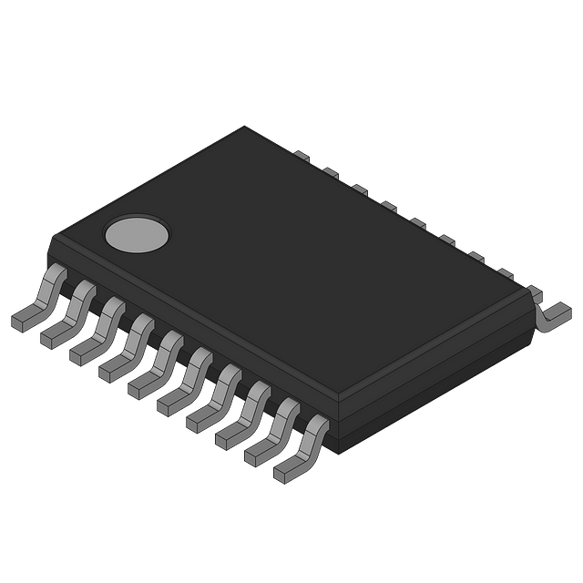
| 封装/外壳 | 20-TSSOP(0.173",4.40mm 宽) |
| 封装/箱体 | TSSOP-20 |
| 工作温度 | -40°C ~ 125°C |
| 工作电源电压 | 12 V |
| 工厂包装数量 | 70 |
| 开关频率 | 1000 kHz |
| 拓扑结构 | Flyback, Forward |
| 最大工作温度 | + 125 C |
| 最小工作温度 | - 40 C |
| 标准包装 | 70 |
| 电压-电源 | 8.5 V ~ 16 V |
| 类型 | Current Mode PWM Controllers |
| 系列 | UCC2897A |
| 设计资源 | http://www.digikey.com/product-highlights/cn/zh/texas-instruments-webench-design-center/3176 |
| 输出数 | 1 |
| 输出电压 | 3 V |
| 输出电流 | 2000 mA |
| 输出端数量 | 1 Output |
| 降压 | 无 |
| 隔离式 | 是 |
| 频率-最大值 | 1MHz |


- 商务部:美国ITC正式对集成电路等产品启动337调查
- 曝三星4nm工艺存在良率问题 高通将骁龙8 Gen1或转产台积电
- 太阳诱电将投资9.5亿元在常州建新厂生产MLCC 预计2023年完工
- 英特尔发布欧洲新工厂建设计划 深化IDM 2.0 战略
- 台积电先进制程称霸业界 有大客户加持明年业绩稳了
- 达到5530亿美元!SIA预计今年全球半导体销售额将创下新高
- 英特尔拟将自动驾驶子公司Mobileye上市 估值或超500亿美元
- 三星加码芯片和SET,合并消费电子和移动部门,撤换高东真等 CEO
- 三星电子宣布重大人事变动 还合并消费电子和移动部门
- 海关总署:前11个月进口集成电路产品价值2.52万亿元 增长14.8%


PDF Datasheet 数据手册内容提取
Product Order Technical Tools & Support & Reference Folder Now Documents Software Community Design UCC2897A SLUS829G–AUGUST2008–REVISEDFEBRUARY2020 UCC2897A Advanced Current-Mode Active-Clamp PWM Controller 1 Features 3 Description • Low-outputjitter The UCC2897A PWM controller simplifies 1 implementation of the various active clamp or reset • Soft-stopshutdownofMAINandAUX andsynchronousrectifierswitchingpowertopologies. • 110-Vinputstartupfunction The UCC2897A is a peak current-mode fixed- • Idealforactive-clamp,reset-forward,flybackand frequency high-performance pulse-width modulator. synchronousrectifieruses The controller includes the logic and the drive • Providescomplementaryauxiliarydriverwith capabilityfortheP-channelauxiliaryswitchalongwith programmabledeadtime(Turn-OnDelay) a simple method of programming the critical delays betweenAUXandMAINswitches forproperactive-clampoperation. • Peakcurrent-modecontrolwith0.5-Vcycle-by- Features include an internal programmable slope cyclecurrentlimiting compensation circuit, precise D limit, and a MAX synchronizable oscillator with an internal-timing • TrueDrive™2-ASink,2-Asourceoutputs capacitor. An accurate line-monitoring function also • Trimmedinternal-bandgapreferenceforaccurate programs the ON and OFF transitions of the lineUVandlineOVthreshold converterwithregardtothebulkinputvoltage,VIN. • Programmableslopecompensation The UCC2897A adds a second-level hiccup-mode • High-performance1-MHzsynchronizableoscillator current-sense threshold, bi-directional withinternaltimingcapacitor synchronization and input-overvoltage protection • Preciseprogrammablemaximumdutycycle functionalities. The UCC2897A is offered in 20-pin TSSOP(PW)and20-pinQFN(RGP)packages. • PB-freeleadfinishpackage DeviceInformation(1) 2 Applications PARTNUMBER PACKAGE BODYSIZE(NOM) • High-efficiencyDC-to-DCpowersupplies TSSOP(20) 6.60mmx6.60mm • Serverpower,48-Vtelecom,datacom,and42-V UCC2897A VQFN(20) 4.15mmx4.15mm automotiveapplications (1) For all available packages, see the orderable addendum at theendofthedatasheet. TypicalApplicationDiagram 1 An IMPORTANT NOTICE at the end of this data sheet addresses availability, warranty, changes, use in safety-critical applications, intellectualpropertymattersandotherimportantdisclaimers.PRODUCTIONDATA.
UCC2897A SLUS829G–AUGUST2008–REVISEDFEBRUARY2020 www.ti.com Table of Contents 1 Features.................................................................. 1 8.3 FeatureDescription.................................................13 2 Applications........................................................... 1 8.4 DeviceFunctionalModes........................................27 3 Description............................................................. 1 9 ApplicationandImplementation........................ 28 4 RevisionHistory..................................................... 2 9.1 ApplicationInformation............................................28 9.2 TypicalApplication .................................................28 5 DeviceOptions....................................................... 3 10 PowerSupplyRecommendations..................... 34 6 PinConfigurationandFunctions......................... 3 11 Layout................................................................... 34 7 Specifications......................................................... 5 11.1 LayoutGuidelines.................................................34 7.1 AbsoluteMaximumRatings......................................5 11.2 LayoutExample....................................................34 7.2 ESDRatings..............................................................5 12 DeviceandDocumentationSupport................. 36 7.3 RecommendedOperatingConditions.......................5 7.4 ThermalInformation..................................................6 12.1 DocumentationSupport .......................................36 7.5 ElectricalCharacteristics...........................................6 12.2 ReceivingNotificationofDocumentationUpdates36 7.6 TimingRequirements ...............................................7 12.3 CommunityResources..........................................36 7.7 TypicalCharacteristics..............................................9 12.4 Trademarks...........................................................36 12.5 ElectrostaticDischargeCaution............................36 8 DetailedDescription............................................ 12 12.6 Glossary................................................................36 8.1 Overview.................................................................12 13 Mechanical,Packaging,andOrderable 8.2 FunctionalBlockDiagram.......................................12 Information........................................................... 37 4 Revision History NOTE:Pagenumbersforpreviousrevisionsmaydifferfrompagenumbersinthecurrentversion. ChangesfromRevisionF(November2017)toRevisionG Page • ChangedModifiedTypicalApplicationdiagram .................................................................................................................... 1 • ChangedUpdatedtheRDEL1calculation............................................................................................................................ 31 • ChangedUpdatedtheRDEL2calculation ........................................................................................................................... 31 ChangesfromRevisionE(April2015)toRevisionF Page • ChangedEquation1From;t =11.1×10⁻²To:t =11.1×10⁻¹².............................................................................. 13 DEL2 DEL2 • ChangedEquation15From:Q xQ To:Q +Q .................................................................................... 31 G(main) G(aux) G(main) G(aux) ChangesfromRevisionD(July2009)toRevisionE Page • AddedESDRatingstable,FeatureDescriptionsection,DeviceFunctionalModes,ApplicationandImplementation section,PowerSupplyRecommendationssection,Layoutsection,DeviceandDocumentationSupportsection,and Mechanical,Packaging,andOrderableInformationsection. ................................................................................................ 1 • ChangedThermalResistanceInformationtabletonewThermalInformationlayoutandupdatedPWandRGP packagedata.......................................................................................................................................................................... 3 • AddedR andR ,R testconditionstoD parameterinthePWMsectionoftheElectricalCharacteristicstable...7 ON OFF DEL MAX • ChangedOscillatorequationsinStep1forR andR ................................................................................................... 30 ON OFF 2 SubmitDocumentationFeedback Copyright©2008–2020,TexasInstrumentsIncorporated ProductFolderLinks:UCC2897A
UCC2897A www.ti.com SLUS829G–AUGUST2008–REVISEDFEBRUARY2020 5 Device Options CYCLE-BY- 110-VHVJFET PARTNUMBER AUXOUTPUT HICCUPMODE APPLICATION CYCLECS START-UP POLARITY THRESHOLD CSTHRESHOLD CIRCUIT TSSOP-20(PW)(1) QFN-20(RGP)(2) DC/DC P-Channel 0.5V 0.75V Yes UCC2897APW UCC2897ARGP (1) ThePWpackageisavailabletapedandreeled.AddRsuffixtothedevicetype(forexample:UCC2897APWR)toorderquantitiesof 2,000devicesperreel.Bulkquantitiesare70unitspertube.TheRGPpackageisavailableintwooptionsoftapeandreel.TheRGPT isorderableinsmallreelsof250(forexample:UCC2897ARGPT);theRGPRcontains3000piecesperreel(forexample: UCC2897ARGPR). (2) TheTSSOP-20(PW)andQFN-20(RGP)packageusesPb-freeleadfinishofPd-Ni-AuwhichiscompatiblewithMSLlevel1at255°C to260°Cpeakreflowtemperatureandcompatiblewitheitherlead-free,tin,orleadsolderingoperations. 6 Pin Configuration and Functions PWPackage 20-PinTSSOP TopView VIN 1 20 N/C N/C 2 19 LINEOV RDEL 3 18 LINEUV RON 4 17 VDD ROFF 5 16 PVDD VREF 6 15 OUT SYNC 7 14 AUX GND 8 13 PGND CS 9 12 SS/SD RSLOPE 10 11 FB RGPPackage 20-PinVQFN BottomView F F C N F E N D O O R Y N R R V S G 1 2 3 4 5 RDEL 20 6 CS NC 19 7 RSLOPE VIN 18 8 FB NC 17 9 SS/SD LINEOV 16 10 PGND 15 14 13 12 11 V D D T X U D D U U E V V O A N P LI Copyright©2008–2020,TexasInstrumentsIncorporated SubmitDocumentationFeedback 3 ProductFolderLinks:UCC2897A
UCC2897A SLUS829G–AUGUST2008–REVISEDFEBRUARY2020 www.ti.com PinFunctions PIN NO. I/O DESCRIPTION NAME TSSOP VQFN Thisoutputdrivestheauxiliary-clampMOSFETwhichturnsonwhenthemain AUX 14 11 O PWM-switchingdeviceturnsoff.TheAUXpindirectlydrivestheauxiliaryswitch witha2-Asourceturn-oncurrentanda2-Asinkturn-offcurrent. Thispinsensesthepeakcurrentutilizedforcurrent-modecontrolandforcurrent- CS 9 6 I limitingfunctions.Thepeaksignalisappliedtothispinbeforepulse-by-pulse currentlimitingactivatesandisapproximately0.5V. Thispinbringstheerrorsignalfromanexternaloptocouplerorerroramplifierinto thePWM-controlcircuitry.Often,thereisaresistortiedfromFBtoVREF,andan FB 11 8 I optocouplerpullsthecontrolpinclosertoGNDtoreducethepulsewidthofthe OUToutputdrivingthemain-powerswitchoftheconverter. Thispinservesasthefundamental-analoggroundforthePWM-controlcircuitry. GND 8 5 ThispinisconnectedtoPGNDdirectlyatthedevice. TheLINEOVpinisaninputpinofvoltagecomparatorwithprogrammable LINEOV 19 16 I hysteresisand1.27-Vthreshold,providingLINEovervoltageorotherfunctions. Thispinprovidesameanstoaccuratelyenable/disablethepowerconverterstage bymonitoringthebulkinputvoltageoranotherparameter.Whenthecircuitinitially starts(orrestartsfromadisabledcondition),arisinginputonLINEUVenablesthe LINEUV 18 15 I outputswhenthethresholdof1.27Viscrossed.Afterthecircuitisenabled,a fallingLINEUVsignaldisablestheoutputswhenthesamethresholdisreached. Thehysteresisbetweenthetwolevelsisprogrammedusinganinternalcurrent source. ThisoutputpindrivesthemainPWMswitchingelementMOSFETinanactive- clampcontroller.TheOUTpindirectlydrivesanN-channeldevicewitha2-A OUT 15 12 O sourceturnon-currentanda2-Asinkturnoff-current.TIrecommendsconnectinga 10-kΩresistorfromthispintoPGNDpin. ThePGNDshouldserveasthecurrentreturnforthehigh-currentoutputdrivers PGND 13 10 OUTandAUX.Ideally,thecurrentpathfromtheoutputstotheswitchingdevices, andbackwouldbeasshortaspossible,andencloseaminimal-looparea. ThePVDDpinisthesupplypinforthepowerdevices.Itisseparatedinternally PVDD 16 13 I fromtheVDDpin. AresistorconnectedfromthispintoGNDprogramsaninternalcurrentsourcethat RSLOPE 10 7 I setstheslope-compensationrampforthecurrent-modecontrol-circuitry. AresistorfromthispintoGNDprogramstheturn-ondelayofthetwogate-drive RTDEL 3 20 I outputstoaccommodatetheresonanttransitionsoftheactive-clamppower converter. AresistorconnectedfromthispintoGNDprogramsaninternal-currentsourcethat ROFF 5 2 I dischargestheinternaltiming-capacitor. AresistorconnectedfromthispintoGNDprogramsaninternal-currentsourcethat RON 4 1 I chargestheinternaltiming-capacitor. AcapacitorfromSS/SDtogroundischargedbyaninternal-currentsourceof SS/SD 12 9 I IRONtoprogramthesoft-startintervalforthecontroller.Duringafaultcondition thiscapacitorisdischargedbyacurrentsourceequaltoI . RON TheSYNCpinservesasabidirectional-synchronizationinputfortheinternal oscillator.Thesynchronizationfunctionisimplementedsuchthattheuser- SYNC 7 4 I programmablemaximumduty-cycle(setbyRONandROFF)remainsaccurate duringsynchronizedoperation.Thispinisleftopenwhennotinuse.Theexternal capacitanceisminimized.Nocapacitorsareconnectedtothispin. TheVDDpinisthepowersupplyforthedevice.Thereshouldbea1-μFcapacitor directlyfromVDDtoPGND.Thecapacitorvalueshouldbeatleast10-timeslarger thanthatonVREF.PGNDandGNDareconnectedexternallyanddirectlyfrom VDD 17 14 I PGNDpintoGNDpin.(TomakeafulldesignofcapacitanceonVDDpin,please referto,ApplicationNote:UnderstandingandDesigninganActiveClampCurrent ModeControlledConverter(SLUA535),section7.3) Thispinisconnectedtotheinput-powerraildirectly.Insidethedevice,ahigh- VIN 1 18 I voltagestart-updeviceisutilizedtoprovidethestart-upcurrentforthecontroller untilabootstrap-typebiasrailbecomesavailable. 4 SubmitDocumentationFeedback Copyright©2008–2020,TexasInstrumentsIncorporated ProductFolderLinks:UCC2897A
UCC2897A www.ti.com SLUS829G–AUGUST2008–REVISEDFEBRUARY2020 PinFunctions(continued) PIN NO. I/O DESCRIPTION NAME TSSOP VQFN TheVREFpinisthe5-Vreferencevoltagethatisusedforanexternalloadofupto 5mA.Sincethisreferenceprovidesthesupplyrailforinternallogic,VREFis VREF 6 3 O bypassedtoAGNDascloseaspossibletothedevice.TheVREFbiasprofileis notalwaysmonotonicbeforeVDDreaches5V. 7 Specifications 7.1 Absolute Maximum Ratings overoperatingfree-airtemperaturerange(unlessotherwisenoted) (1) MIN MAX UNIT V Lineinputvoltage 120 IN V Supplyvoltage 16.5 V DD Analoginputs,FB,CS,SYNC,LINEOV,LINEUV –0.3 (V +0.3) REF I Outputsourcecurrent(peak)OUTAUX 2.5 O_SOURCE A I Outputsinkcurrent(peak)OUTAUX –2.5 O_SINK T Operatingjunctiontemperaturerange –55 150 J °C T Leadtemperature,1,6mm(1/16inch)fromcasefor10seconds 300 sol T Storagetemperature –65 150 °C stg (1) StressesbeyondthoselistedunderAbsoluteMaximumRatingsmaycausepermanentdamagetothedevice.Thesearestressratings only,whichdonotimplyfunctionaloperationofthedeviceattheseoranyotherconditionsbeyondthoseindicatedunderRecommended OperatingConditions.Exposuretoabsolute-maximum-ratedconditionsforextendedperiodsmayaffectdevicereliability. 7.2 ESD Ratings VALUE UNIT Human-bodymodel(HBM),perANSI/ESDA/JEDECJS-001(1) ±2000 V(ESD) Electrostaticdischarge Charged-devicemodel(CDM),perJEDECspecificationJESD22- ±500 V C101(2) (1) JEDECdocumentJEP155statesthat500-VHBMallowssafemanufacturingwithastandardESDcontrolprocess. (2) JEDECdocumentJEP157statesthat250-VCDMallowssafemanufacturingwithastandardESDcontrolprocess. 7.3 Recommended Operating Conditions overoperatingfree-airtemperaturerange(unlessotherwisenoted) MIN NOM MAX UNIT V Lineinputvoltage 18 110 V IN V Supplyvoltage 8.5 12 16 V DD V Supplybypasscapacitance 1 µF DD R =R Timingresistance(for250-kHz 75 kΩ ON OFF operation) T Operatingjunctiontemperature –40 125 °C J C Referencebypasscapacitance 0.1 µF REF Copyright©2008–2020,TexasInstrumentsIncorporated SubmitDocumentationFeedback 5 ProductFolderLinks:UCC2897A
UCC2897A SLUS829G–AUGUST2008–REVISEDFEBRUARY2020 www.ti.com 7.4 Thermal Information UCC2897A THERMALMETRIC(1) QFN(RGP) TSSOP(PW) UNIT 20PINS 20PINS R Junction-to-ambientthermalresistance 34.1 91.6 θJA R Junction-to-case(top)thermalresistance 33.3 26.3 θJC(top) R Junction-to-boardthermalresistance 9.2 42.6 θJB °C/W ψ Junction-to-topcharacterizationparameter 0.4 1.1 JT ψ Junction-to-boardcharacterizationparameter 9.1 42.1 JB R Junction-to-case(bottom)thermalresistance 2.9 N/A θJC(bot) (1) Formoreinformationabouttraditionalandnewthermalmetrics,seetheSemiconductorandICPackageThermalMetricsapplication report. 7.5 Electrical Characteristics V =12V(1),1-µFcapacitorforVDDtoGND,0.01-µFcapacitorfromVREFtoGND,R =R =75kΩ,R =50kΩ, DD ON OFF SLOPE –40°C≤T =T ≤125°C(unlessotherwisenoted) A J PARAMETER TESTCONDITIONS MIN TYP MAX UNIT OVERALL I Start-upcurrent V <V 300 500 µA STARTUP DD UVLO V =0V, FB I Operatingsupplycurrent(1)(2) V =0V, 2 3 mA DD CS Outputsnotswitching HIGH-VOLTAGEBIAS CurrentavailablefromVDDduring I VDDstartupcurrent startup,T =–40°Cto+85°C,V = 4 11 mA DD-ST A IN 36V(3) I JFETleakagecurrent VIN=120V;VDD=14V 75 µA VIN UNDERVOLTAGELOCKOUT UVLO Startthresholdvoltage 12.2 12.7 13.2 Minimumoperatingvoltageafter 7.6 8 8.4 V start Hysteresis 4.4 4.7 5 LINEMONITOR V LineUVvoltagethreshold 1.243 1.268 1.294 V LINEUV I LineUVhysteresiscurrent –11.5 –13 –14.5 µA LINEUVHYS V LineOVvoltagethreshold 1.243 1.268 1.294 V LINEOV I LineOVhysteresiscurrent –11.5 –13 –14.5 µA LINEOVHYS Soft-Start I SSchargecurrent R =75kΩ(4) –10.5 –14.5 –18.5 SSC ON µA I SSdischargecurrent R =75kΩ(4) 10.5 14.5 18.5 SSD ON Discharge/shutdownthreshold V 0.4 0.5 0.6 V SS/SD voltage VOLTAGEREFERENCE V Referencevoltage T =25°C 4.85 5 5.15 REF J V V Referencevoltage 0A<I <5mA,overtemperature 4.75 5 5.25 REF REF I Shortcircuitcurrent REF=0V,T =25°C –20 –11 –8 mA SC J INTERNALSLOPECOMPENSATION (1) SetVDDabovethestartthresholdbeforesettingat12V. (2) Doesnotincludecurrentoftheexternaloscillatornetwork. (3) ThepowersupplystartswithI loadonVDD,thepartstartsupwithnoloadupto125°C.Formoreinformationseethesectionfor DD–ST VINandVDD (4) I andI aredirectlyproportionaltoI .SeeEquation8. SSC SS/SD RON 6 SubmitDocumentationFeedback Copyright©2008–2020,TexasInstrumentsIncorporated ProductFolderLinks:UCC2897A
UCC2897A www.ti.com SLUS829G–AUGUST2008–REVISEDFEBRUARY2020 Electrical Characteristics (continued) V =12V(1),1-µFcapacitorforVDDtoGND,0.01-µFcapacitorfromVREFtoGND,R =R =75kΩ,R =50kΩ, DD ON OFF SLOPE –40°C≤T =T ≤125°C(unlessotherwisenoted) A J PARAMETER TESTCONDITIONS MIN TYP MAX UNIT R / m Slope FB=High –10% CS +10% R SLOPE OSCILLATOR T =25°C 237 250 265 J fOSC Oscillatorfrequency –40°C<TJ<125°C;8.5V<VDD< 225 270 kHZ 14.5V V Oscillatoramplitude(peak-to-peak) 2 V P_P SYNCHRONIZATION SYNCinputhighvoltage 3 V SYNCinputlowvoltage 1.6 SYNCpulldownoutputcurrent 600 µA SYNCpullupoutputcurrent –600 SYNCoutputpulsewidth 150 ns t SYNC-to-outputdelay 50 DEL PWM(5) D Maximumdutycycle R =R =75kΩ,R =10kΩ 66% 70% 74% MAX ON OFF DEL Minimumdutycycle 0% PWMoffset CS=0V 0.43 0.5 0.61 V CURRENTSENSE V Currentsenselevelshiftvoltage 0.4 0.5 0.6 LVL V Maximumvoltageerror(clamped) 5 ERR(max) V Currentsensethresholdcycle-by- V 0.43 0.48 0.53 CS cycle OUTPUT(OUTANDAUX) I Outputsourcecurrent –2 OUT(src) A I Outputsinkcurrent 2 OUT(sink) V Low-leveloutputvoltage I =150mA 0.4 OUT(low) OUT V V High-leveloutputvoltage I =–150mA 11.1 OUT(high) OUT (5) MaximumpulsewidthneedstobelessthanD ,whichisafunctionofRONandR .FormoreinformationonD ,seedetailed MAX OFF MAX descriptionforR in. OFF 7.6 Timing Requirements MIN NOM MAX UNIT OUTPUT(OUTANDAUX) t Risetime C =2nF 19 28 R LOAD t Falltime C =2nF 14 23 F LOAD tDEL1 Delaytime(AUXtoOUT) CLOAD=2nF,RDEL=10 110 ns kΩ t Delaytime(OUTtoAUX) C =2nF,R =10 115 DEL2 LOAD DEL kΩ Copyright©2008–2020,TexasInstrumentsIncorporated SubmitDocumentationFeedback 7 ProductFolderLinks:UCC2897A
UCC2897A SLUS829G–AUGUST2008–REVISEDFEBRUARY2020 www.ti.com 50% 50% t OUT AUX 50% 50% t (P--channel) t t DEL1 DEL2 Figure1. OutputTimingDiagram 8 SubmitDocumentationFeedback Copyright©2008–2020,TexasInstrumentsIncorporated ProductFolderLinks:UCC2897A
UCC2897A www.ti.com SLUS829G–AUGUST2008–REVISEDFEBRUARY2020 7.7 Typical Characteristics 14 2.5 12 V UVLOOn -- 2.0 olds10 mA geThresh 8 UVLOOff Current-- 1.5 OVolta 6 Supply 1.0 VL -- --U 4 UVLOHysteresis IDD O VL 0.5 U V 2 0 0 --50 --25 0 25 50 75 100 125 0 2 4 6 8 10 12 14 16 TJ -- JunctionTemperature--°C VDD--SupplyVoltage--V Figure2.UVLOVoltageThresholdsvs.Junction Figure3.QuiescentCurrentvs.SupplyVoltage Temperature 10 20 VIN=36V 0 A 15 m mA --10 nt-- Current-- --20 DDCurre 10 y V --SupplD --30 JFETSourceCurrent External 5 D I --40 0 --50 --50 --25 0 25 50 75 100 125 0 2 4VDD--S6upply8Voltag1e0--V 12 14 16 TJ -- JunctionTemperature--°C Figure5.TypicalStartupCurrentAvailableFromVDDvs. Figure4.SupplyCurrentvs.SupplyVoltage Temperature 1.30 20 A 15 μ 1.28 -- SoftstartDischargeCurrent s V nt 10 ds-- urre Threshol 1.26 oftstartC 50 e S V--LinTH 11..2224 /I--DIS)SS(CHG) --1--50 ISS( --15 SoftstartChargeCurrent 1.20 --20 --50 --25 0 25 50 75 100 125 --50 --25 0 25 50 75 100 125 TJ -- JunctionTemperature--°C TJ -- JunctionTemperature--°C Figure6.LineUV/OVVoltageThresholdvs.Junction Figure7.SoftstartCurrentsvs.Temperature Temperature Copyright©2008–2020,TexasInstrumentsIncorporated SubmitDocumentationFeedback 9 ProductFolderLinks:UCC2897A
UCC2897A SLUS829G–AUGUST2008–REVISEDFEBRUARY2020 www.ti.com Typical Characteristics (continued) 0.60 10M V e-- 0.58 g a dVolt 0.56 Hz 1M hreshol 00..5542 uency-- T q art/Shutdown 000...454608 SwitchingFre100K st -- Soft 0.44 fSW 10K -- VTH 0.42 0.40 1K --50 --25 0 25 50 75 100 125 10 100 1000 TJ -- JunctionTemperature--°C RON=ROFF--TimingResistance--kΩ Figure8.SoftStart/ShutdownThresholdVoltagevs. Figure9.SwitchingFrequencyvs.ProgrammingResistance JunctionTemperature 275 74 RON=ROFF=75kΩ RON=ROFF=75kΩ 270 73 kHz 265 % 72 gFrequency-- 222556050 mDutyCycle-- 7701 --SwitchinW 224450 --MaximuAX6698 fS 235 DM 230 67 225 66 --50 --25 0 25 50 75 100 125 --50 --25 0 25 50 75 100 125 TJ -- JunctionTemperature--°C TJ -- JunctionTemperature--°C Figure10.OscillatorFrequencyvs.JunctionTemperature Figure11.MaximumDutyCyclevs.JunctionTemperature 1.4 2.50 V oltage--V 1.2 Voltage-- 22..4450 V 1.0 d hreshold 0.8 Threshol 2.35 T n 2.30 nse HiccupMode atio CurrentSe 00..46 Cycle-by-CycleCurrentLimit Synchroniz 22..2205 V--CS 0.2 --YNC 2.15 S V 2.10 0 --50 --25 0 25 50 75 100 125 --50 --25 0 25 50 75 100 125 TJ -- JunctionTemperature--°C TJ -- JunctionTemperature--°C Figure12.CurrentSenseThresholdVoltagevs.Junction Figure13.SynchronizationThresholdVoltagevs.Junction Temperature Temperature 10 SubmitDocumentationFeedback Copyright©2008–2020,TexasInstrumentsIncorporated ProductFolderLinks:UCC2897A
UCC2897A www.ti.com SLUS829G–AUGUST2008–REVISEDFEBRUARY2020 Typical Characteristics (continued) 25 800 CLOAD=2nF RiseTime 700 --ns 20 600 ttDDEELL12 es ns RiseandFallTim 1105 FallTime --DelayTime--EL 345000000 /t--RF tD 200 t 5 100 0 0 0 10 20 30 40 50 60 70 --50 --25 TJ0-- Junc2t5ionTe5m0peratu7r5e--°C100 125 RDEL--DelayResistance--kΩ Figure15.DelayTimevs.DelayResistance Figure14.OutAndAUXRiseAndFallTimevs.Junction Temperature 250 800 RDEL=10kΩ RDEL=50kΩ 700 200 600 ns OUTtoAUX μs me-- 150 me-- 500 AUXtoOUT Ti Ti OUTtoAUX Delay Delay 400 t--DEL 100 t--DEL 300 200 50 AUXtoOUT 100 0 0 --50 --25 0 25 50 75 100 125 --50 --25 0 25 50 75 100 125 TJ -- JunctionTemperature--°C TJ -- JunctionTemperature--°C Figure16.DelayTimevs.JunctionTemperature Figure17.DelayTimevs.JunctionTemperature 5.3 NoLoad 10mALoad 5.2 V -- e ag 5.1 olt V e c en 5.0 er ef R -- 4.9 EF R V 4.8 4.7 --50 --25 0 25 50 75 100 125 TJ -- JunctionTemperature--°C Figure18.ReferenceVoltagevs.Temperature Copyright©2008–2020,TexasInstrumentsIncorporated SubmitDocumentationFeedback 11 ProductFolderLinks:UCC2897A
UCC2897A SLUS829G–AUGUST2008–REVISEDFEBRUARY2020 www.ti.com 8 Detailed Description 8.1 Overview The UCC2897A is a peak current mode active clamp PWM controller. It provides simple interface to program the critical timings such as soft start, gate turn on delay, switching period, maximum operating duty cycle, and slope compensation. Features includes a high voltage JFET circuit, UVLO protection, line under/over voltage protection, pulse skipping, and synchronization. The UCC2897A also has the logic and the drive capability for a P-channelauxiliaryswitch.TheVDDsupplyisgeneratedfromabootstrapcircuitconnectedtoabiaswinding. 8.2 Functional Block Diagram VIN 1 2.5 V N/C 2 VREF IRDEL 20 N/C RDEL 3 VREF 0.05 x IRDEL 2.5 V CLOCK 0.05 x IRDEL 19 LINEOV ICHG Start LineOV 1.27 V End RTON 4 LineU 18 LINEUV 2.5 V 1 - DMAX V 1.V27 13V / 8V IDSCHG VDD CT RTOFF 5 OUT PWM VREF 17 VDD SYNC OFF VDD IRDEL 16 PVDD OUT VREF 6 GREENF S Q Turn-on Delay 15 OUT RD Q VREF GND SYNC 7 IRDEL 14 AUX + 0.5 V GND Turn-on Delay GND 8 13 PGND VREF VREF 0.43 x ICHG 5 x ISLOPE CS 99 12 SS/SD ISLOPE CT 1 - DMAX R 4 x R LiVnVReDUEDVF UVLO & SS Enable 0.43 x ICHG LineOV RSLOPE 10 11 FB Copyright © 2017, Texas Instruments Incorporated 12 SubmitDocumentationFeedback Copyright©2008–2020,TexasInstrumentsIncorporated ProductFolderLinks:UCC2897A
UCC2897A www.ti.com SLUS829G–AUGUST2008–REVISEDFEBRUARY2020 8.3 Feature Description 8.3.1 DetailedPinDescriptions 8.3.1.1 RDEL This pin is internally connected to an approximately 2.5-V DC source. A resistor (RDEL) to GND sets the turn-on delay for both gate drive signals of the UCC2987A controller. The delay time is identical for both switching transitions between OUT turning off and AUX turning on, as well as when AUX is turning off and OUT is turning on.ThedelaytimeisdefinedinEquation1. t =t =11.1×10⁻¹²×R +15×10–9seconds (1) DEL1 DEL2 DEL For proper selection of the delay time refer to the various references describing the design of active-clamp power-converters. 8.3.1.2 RON This pin is internally connected to an approximately 2.5-V DC source. A resistor (R ) to GND (pin 6) sets the ON charge current of the internal-timing capacitor. The RON pin, in conjunction with the ROFF pin (pin 3), sets the operatingfrequencyandmaximum-operatingdutycycle. 8.3.1.3 ROFF This pin is internally connected to an approximately 2.5-V DC source. A resistor (R ) to GND (pin 6) sets the OFF discharge current of the internal-timing capacitor. The RON and ROFF pins set the switching period (T ) and SW maximum-operatingdutycycle(D )accordingtothefollowingequations: MAX tON =36.1´10-12´RON´æçSö÷-tDEL(s) seconds èWø (2) tOFF =15´10-12´ROFF´æçSö÷+tDEL(s)+170´10-9´(s) seconds èWø (3) T =t +t (4) SW ON OFF t D = ON MAX t +t ON OFF (5) 8.3.1.4 VREF The internal 5-V bias rail of the controller is connected to this pin. The internal bias-regulator requires a high- quality ceramic-bypass capacitor (C ) to GND for noise filtering and to provide compensation to the regulator VREF circuitry.TherecommendedC valueis0.22μFandX7Rcapacitorsarerecommended.Theminimum-bypass VREF capacitor value is 0.022 μF limited by stability considerations of the bias regulator, while the maximum is approximately22μF.ThecapacitanceonVREFandVDDshouldbeinaminimumratioof1:10. The VREF pin is internally current-limited and supplies approximately 5 mA to external circuits. The 5-V bias is available only when the undervoltage lock-out (UVLO) circuit enables the operation of UCC2897A controller. The VREF-biasprofilemaynotbemonotonicbeforeVDDreaches5V. For the detailed functional description of the undervoltage lock-out (UVLO) circuit refer to the section of this datasheet. Copyright©2008–2020,TexasInstrumentsIncorporated SubmitDocumentationFeedback 13 ProductFolderLinks:UCC2897A
UCC2897A SLUS829G–AUGUST2008–REVISEDFEBRUARY2020 www.ti.com Feature Description (continued) 8.3.1.5 SYNC Thispinisabi-directionalsynchronizationterminal.Thispinshouldbeleftopenifnotused. This pin provides an input for an external-clock signal which synchronizes the internal oscillator of the UCC2897A controller. The synchronizing frequency must be higher than the free-running frequency of the onboard oscillator (T < T ). The acceptable minimum pulse-width of the synchronization signal is SYNC SW approximately50ns(positivelogic),andshouldremainshorterthanEquation6. (1–D )×T MAX SYNC where • D issetbyR andR (6) MAX ON OFF If the pulse-width of the synchronization signal stays within these limits, the maximum-operating duty ratio remains valid as defined by the ratio of RON and ROFF, and DMAX is the same in free-running and in synchronized modes of operation. If the pulse width of the synchronization signal would exceed the (1 – D ) × MAX T limit,themaximum-operatingdutycycleisdefinedbythesynchronizationpulsewidth. SYNC In the stand-alone mode, the sync pin is driven by the internal oscillator which provides output pulses. The pulse width from SYNC output does not vary with the duty cycle. That signal synchronizes other PWM controllers or circuitsrequiringaconstant-frequencytimebase. External capacitance should be minimized on this pin layout. Capacitors are not connected between SYNC and GNDorPGND.FormoreinformationonsynchronizationoftheUCC2897Arefertothesectionofthisdatasheet. 8.3.1.6 GND This pin provides a reference potential for all small-signal control and programming circuitry inside the UCC2897A.Groundlayoutiscriticalforcorrectoperation. High-current surges from the MOSFET drivers conduct through PVDD, OUT, AUX, and PGND. To localize these surges, PVDD must bypass directly to PGND. PGND current must be electrically, capacitively, and inductively isolated from GND with only one short trace connecting PGNDtoGND,locatedtobestminimizenoiseintoGND. 8.3.1.7 CS CS is a direct input to the PWM and current-limit comparators of the UCC2897A controller. The CS pin never connects directly across the current-sense resistor (R ) of the power converter. A small, customary R-C filter CS between the current-sense resistor and the CS pin is necessary to accommodate the proper operation of the onboard slope-compensation circuit and in order to protect the interna- discharge transistor connected to the CS pin(R ,C ). F1 F Slope compensation is achieved across RF by a linearly-increasing current flowing out of the CS pin. The slop- compensation current is only present during the on-time of the gate-drive signal of the main-power switch (OUT) of the converter. The internal-pulldown transistor of the CS pin is activated during the discharge time of the timing capacitor. This time interval is (1 – D ) × T long and represents the specified off-time of the main- MAX SW powerswitch. 14 SubmitDocumentationFeedback Copyright©2008–2020,TexasInstrumentsIncorporated ProductFolderLinks:UCC2897A
UCC2897A www.ti.com SLUS829G–AUGUST2008–REVISEDFEBRUARY2020 Feature Description (continued) 8.3.1.8 RSLOPE A resistor (R ) connected between this pin and GND (pin 6) sets the amplitude of the slope-compensation SLOPE current. During the on time of the main gate-drive output (OUT) the voltage across R is a representation of SLOPE the internal-timing-capacitor waveform. As the timing capacitor is being charged, the voltage across R also SLOPE increases, generating a linearly-increasing current waveform. The current provided at the CS pin for slope compensationisproportionaltothiscurrentflowingthroughR . SLOPE Due to the high speed, AC-voltage waveform present at the RSLOPE pin, the parasitic capacitance and inductanceoftheexternal-circuitcomponentsconnectedtotheRSLOPEpinshouldbecarefullyminimized. Formoreinformationonhowtoprogramtheinternal-slopecompensationrefertothesectionofthisdatasheet. 8.3.1.9 FB FB and SS/SD interact. The one with the lower-voltage value takes control on the duty cycle, refer to SS/SD description. This pin is an input for the control voltage of the pulse-width modulator of the UCC2897A.The control voltage is generated by an external-error amplifier by comparing the output voltage of the converter to a voltage reference and employing the compensation for the voltage-regulation loop. Usually, the error amplifier is located on the secondary side of the isolated-power converter and the output voltage is sent across the isolation boundary by an optocoupler. Thus, the FB pin is usually driven by the optocoupler. An external-pullup resistor to theVREFpin(pin4)isalsorequiredforproperoperationaspartofthefeedbackcircuitry. The control voltage is internally buffered and connected to the PWM comparator through a voltage divider to make it compatible to the signal level of the current-sense circuit. The useful voltage range of the FB pin is between approximately 2.5 V and 4.5 V. Control voltages below the 2.5-V threshold result in zero-duty cycle (pulseskipping)whilevoltagesabove4.5Vresultinfull-duty-cycle(D )operation. MAX 8.3.1.10 SS/SD A capacitor (C ) connected between this pin and GND (pin 6) programs the soft-start time of the power SS converter. The soft-start capacitor is charged by a precise, internal DC-current source which is programmed by theR resistorconnectedtopin2.Thesoft-startcurrentisdefinedinEquation7. ON V 1 I =0.43´I =0.43´ REF ´ SS RON 2 R ON (7) This DC current charges C from 0 V to approximately 5 V. Internal to the UCC2897A, the soft-start capacitor SS voltageisbuffered and ORed with the control voltage present at the FB pin (pin 9). The lower of the two voltages manipulates the PWM engine of the controller through the voltage divider described with regards to the FB pin. Accordingly, the useful control range on the SS pin is similar to the control range of the FB pin and it is between 2.5Vand 4.5 V approximately. During line-undervoltage protection, the PWM follows this pin-capacitor discharge toachievesoft-stopfunction Copyright©2008–2020,TexasInstrumentsIncorporated SubmitDocumentationFeedback 15 ProductFolderLinks:UCC2897A
UCC2897A SLUS829G–AUGUST2008–REVISEDFEBRUARY2020 www.ti.com Feature Description (continued) 8.3.1.11 PGND This pin serves as a dedicated connection to all high-current circuits inside the UCC2897A. The high-current portion of the controller consists of the two high-current gate drivers, and the various bias connections except VREF (pin 4). The PGND (pin 11) and GND (pin 6) pins are not connected internally, a low-impedance external connection between the two ground pins is also required. TI recommends to form a separate ground plane for the low-current setup components (R , R , R , C , C , R , C and the emitter of the optocoupler in DEL ON OFF VREF F SLOPE SS the feedback circuit). This separate ground plane (GND) should have a single connection to the rest of the groundofthepowerconverter(PGND)andthisconnectionshouldbebetweenpin6andpin11ofthecontroller. 8.3.1.12 AUX AUX is a high-current gate-drive output for the auxiliary switch to implement the active-clamp operation for the power stage. The auxiliary output (AUX) of the UCC2897A drives a P-channel device as the clamp switch thereforeitrequiresanactive-lowoperation(theswitchisONwhentheoutputislow). 8.3.1.13 OUT This high-current output drives an external N-channel MOSFET. The UCC2897A controller uses an active-high drivesignalforthemainswitchoftheconverter. Due to the high-speed and high-drive current capability of these outputs (AUX, OUT) the parasitic inductance of the external-circuit components connected to these pins should be carefully minimized. A potential way of avoiding unnecessary parasitic inductances in the gate-drive circuit is to place the controller in close proximity to the MOSFETs and by ensuring that the outputs (AUX, OUT) and the gates of the MOSFET devices are connected by wide overlapping traces. TI recommends connecting a 10-kΩ resistor from this pin to PGND pin to reduceapossibleparasiticeffectfromlayout. 8.3.1.14 VDD The VDD rail is the primary bias for the internal high-current gate drivers, the internal 5-V bias regulator and for parts of the undervoltage-lockout circuit. To reduce switching noise on the bias rail, a good-quality ceramic capacitor (C ) must be placed very closely between the VDD pin and PGND (pin 11) to provide adequate HF filtering. The recommended C value is 1-μF for most applications but the value might be affected by the HF propertiesoftheexternal-MOSFETtransistorsusedinthepowerstage. In addition to the low-impedance high-frequency filtering, the bias rail of the controller requires a larger value energy-storage capacitor (C ) connected parallel to C . The energy-storage capacitor must provide the hold- BIAS HF up time to operate the UCC2897A (including gate-drive power requirements) during start up. In steady-state operation the controller must be powered from a bootstrap winding off the power transformer or by an auxiliary- bias supply. In case of an independent-auxiliary-bias supply, the energy storage is provided by the output capacitance of the bias supply. The capacitor values are also determined by the capacitor values connected to VREF.ThecapacitanceonVREFandVDDshouldbeinaminimumratioof1:10. 16 SubmitDocumentationFeedback Copyright©2008–2020,TexasInstrumentsIncorporated ProductFolderLinks:UCC2897A
UCC2897A www.ti.com SLUS829G–AUGUST2008–REVISEDFEBRUARY2020 Feature Description (continued) 8.3.1.15 LINEUV This input monitors the incoming-power source to provide an accurate undervoltage-lockout function with user- programmable hysteresis for the power supply controlled by the UCC2897A. The unique property of the UCC2897A is to use only one pin to implement these functions without sacrificing on performance. The input voltage of the power supply is scaled to the precise 1.27-V threshold of the undervoltage-lockout comparator by an external-resistor divider (R , R in ). Once the input threshold of the line monitor is exceeded, an internal- IN1 IN2 current source gets connected to the LINEUV pin. The current generator is programmed by the R resistor DEL connectedtopin1ofthecontroller.TheactualcurrentlevelisgiveninEquation8. V 1 I = REF ´ ´0.05 HYST 2 R DEL (8) As this current flows through R of the input divider, the undervoltage-lockout hysteresis is a function of I IN2 HYST and R allowing accurate programming of the hysteresis of the line-monitoring circuit. When LINEUV is IN2 detected, PWM follows VSS capacitor discharge and soft-stop function is provided. The soft-start capacitor starts discharging when the soft-start capacitor voltage reaches 2.5 V. Both OUT and AUX stop switching while the soft-start capacitor continues discharging until the voltage reaches 0.5 V when the soft start is resumed on the assumptionofallothersoft-startconditionsaremet. Formoreinformationonhowtoprogramtheline-monitoringfunctionrefertotheofthisdatasheet. 8.3.1.16 VIN The UCC2897A controller is equipped with a high-voltage N-channel-JFET startup device to initiate operation from the input-power source of the converter in applications where the input voltage does not exceed the 110-V maximum rating of the startup transistor. In these applications, the VIN pin connects directly to the positive terminal of the input-power source. The internal-JFET startup transistor provides charge-current for the energy- storage capacitor (C ) connected across the VDD (pin 14) and PGND (pin 11) terminals. Note that the startup BIAS device turns off immediately when the voltage on the VDD pin exceeds approximately 12.7 V, the undervoltage- lockout threshold of the controller for turn-on. The JFET is also disabled at all times when the high-current gate drivers are switching to protect against excessive-power dissipation and current through the device. For dependablestart-up,VDDmustnotbeloadedbymorethan4mA. FormoreinformationonbiasingtheUCC2897A,refertotheandsectionsofthisdatasheet. 8.3.1.17 LINEOV This input monitors the incoming-power source to provide an accurate-overvoltage protection with user- programmable hysteresis for the power supply controlled by the controller. The circuit implementation of the overvoltage-protection function is identical to the technique used for monitoring the input-power rail for undervoltage lockout. The circuit implements an accurate threshold and hysteresis using only one pin. The input voltage of the power supply is scaled to the precise 1.27-V threshold of the overvoltage-protection comparator by an external-resistor divider (R , R in ). Once the input threshold of the line monitor is exceeded, an internal- IN3 IN4 current source gets connected to the LINEOV pin. The current generator is programmed by the R resistor DEL connectedtopin1ofthecontroller.TheactualcurrentlevelisgiveninEquation9. V 1 I = REF ´ ´0.05 HYST 2 R DEL (9) As this current flows through RIN4 of the input divider, the overvoltage-protection hysteresis is a function of I HYST andR allowingaccurateprogrammingofthehysteresisoftheline-monitoringcircuit. IN4 Formoreinformationonhowtoprogramtheovervoltageprotection,refertotheofthisdatasheet. Copyright©2008–2020,TexasInstrumentsIncorporated SubmitDocumentationFeedback 17 ProductFolderLinks:UCC2897A
UCC2897A SLUS829G–AUGUST2008–REVISEDFEBRUARY2020 www.ti.com Feature Description (continued) 8.3.2 JFETControlandUVLO The UCC2897A controller includes a high-voltage JFET startup-transistor. The steady-state power-consumption of the of the control circuit which also includes the gate-drive power-loss of the two power switches of an active- clamp converter exceeds the current and thermal capabilities of the device. Thus the JFET should only be used for initial start-up of the control circuitry and to provide keep-alive power during stand-by mode when the gate- drive outputs are not switching. Accordingly, the startup device is managed by the control algorithm implemented on board the UCC2897A. The following timing diagram in Figure 19 illustrates the operation of the JFET startup device. VON V IN 12.7V 10.0V 8V<VDD<10V 8.0V V Bootstrapbias DD JFET OFF OFF OFF ENABLE (Seediagramonp.6) SS/SD OFF OFF SWITCHING OFF OUTPUTs SWITCHING UDG--03148 Valuesaretypicalinthedrawing. Figure19. JFETControlStartupandShutdown During initial power-up the JFET is on and charges the C and C capacitors connected to the VDD pin. The BIAS HF undervoltage lockout-circuit of the controller monitors the VDD pin to ensure proper biasing before the operation is enabled. When the VDD voltage reaches approximately 12.7 V (UVLO turnon threshold) the UVLO circuit enables the rest of the controller. At that time, the JFET turns off and 5 V appears on the VREF terminal. Switching waveforms might not appear at the gate-drive outputs unless all other conditions of proper operation aremet.Theseconditionsare: • ThevoltageontheCSpinisbelowthecurrentlimitthreshold • Thecontrolvoltageisabovethezeroduty-cycleboundary(V >2.5V). FB • Theinputvoltageisinthevalidoperatingrange(V <V <V . VON VIN VOFF – Thelineunderorovervoltageprotectionsarenotactivated. 18 SubmitDocumentationFeedback Copyright©2008–2020,TexasInstrumentsIncorporated ProductFolderLinks:UCC2897A
UCC2897A www.ti.com SLUS829G–AUGUST2008–REVISEDFEBRUARY2020 Feature Description (continued) As the controller starts operation it draws bias power from the C capacitor until the bootstrap winding takes BIAS over (referring to Figure 25 and Figure 26). During this time, VDD voltage is falling rapidly as the JFET is off but the bootstrap voltage is still not sufficient to power the control circuits. It is imperative to store enough energy in C to prevent the bias voltage from dipping below the turnoff threshold of the UVLO circuit during the startup- BIAS time interval. Otherwise the power supply goes through several cycles of retry attempts before steady-state operationisestablished. During normal operation the bias voltage is determined by the bootstrap bias design. The UCC2897A tolerates a wide range of bias voltages between the minimum-operating voltage (UVLO turn-off threshold) and the maximum-operatingvoltageasdefinedinthe. In applications where the power supply enters standby in response to an external command, the bias voltage of the controller must be kept alive to react intelligently to the control signal. In standby mode, switching action is suspended for an undefined period of time and the bootstrap power is unavailable to bias the controller. Without an alternate power source the bias voltage collapses and the controller initiates a re-start sequence. To avoid this situation, the onboard JFET of the UCC2897A controller keeps the VDD bias alive as long as the gate-drive outputs remain inactive. As shown in the timing diagram in Figure 19, the JFET turns on when VDD = 10 V and charges the C capacitor to approximately 12.7 V. At that time the JFET turns off and VDD gradually BIAS decreases to 10 V then the procedure repeats. When the power supply is enabled again, the controller is fully biased and ready to initiate the soft-start sequence. As soon as the gate-drive pulses appear the JFET turn off andbiasisprovidedbythebootstrapbiasgenerator. During power down the situation is different as the switching action continues until the VDD bias voltage drops below the UVLO turn-off threshold of the controller (approximately 8 V). At that time the UCC2897A shuts down and turns off the 5-V bias rail and returning to startup state when the JFET device is turned on and the C BIAS capacitor starts charging again. In case the input voltage of the converter is re-established, the UCC2897A attemptstorestarttheconverter. Copyright©2008–2020,TexasInstrumentsIncorporated SubmitDocumentationFeedback 19 ProductFolderLinks:UCC2897A
UCC2897A SLUS829G–AUGUST2008–REVISEDFEBRUARY2020 www.ti.com Feature Description (continued) 8.3.3 LineUndervoltageProtection As shown in Figure 20, when the input power-source is removed, the power supply is turned off by the line- undervoltage protection because the bootstrap winding keeps the VDD bias up as long as switching takes place in the power stage. As the input voltage of the power supply decreases gradually toward the line-cutoff voltage, the operating duty cycle of the converter must compensate for the lower input voltage. At minimum input-voltage the duty cycle nears the maximum value (D ). Under these conditions the voltage across the clamp capacitor MAX approaches the highest value since the transformer must be reset in a relatively short time. The timing diagram in Figure 20 highlights that in the instance when the converter stops switching the clamp-capacitor voltage might be at the maximum level. Since the only load of the clamp capacitor is the power transformer, this high voltage could linger across the clamp capacitor for a long time when the converter is off. With this high voltage present across the clamp capacitor a soft start would be very dangerous, due to the narrow duty cycle of the main switch and the long on-time of the clamp switch. This could cause the power transformer to saturate during the next soft-startcycle. VOFF VIN VCLAMP,MAX VCLAMP VSS TSW OUT AUX Figure20. LineUndervoltageShutdownWaveforms,P-Channel To eliminate this potential hazard the UCC2897A controller, discharge the clamp capacitor during power down safely. The OUT and the AUX output continues switching while the soft-start capacitor C is being slowly SS discharged. the function of soft stop is achieved because the AUX pulse-width gradually increases as the clamp voltagedecreases,whileneverapplyingthehighvoltageacrossthetransformerforextendedperiodoftime. 20 SubmitDocumentationFeedback Copyright©2008–2020,TexasInstrumentsIncorporated ProductFolderLinks:UCC2897A
UCC2897A www.ti.com SLUS829G–AUGUST2008–REVISEDFEBRUARY2020 Feature Description (continued) 8.3.4 LineOvervoltageProtection When the line-overvoltage protection is triggered in the UCC2897A controller, the gate-drive signals are immediately disabled. At the same time, the slow discharge of C initiates. While the soft-start capacitor SS discharges the gate-drive signals remain disabled. Once V = 0.5 V and the overvoltage disappears from the SS input of the power supply, operation resumes through a regular soft start of the converter as it is demonstrated in Figure21.ThepulsesofOUTandAUXstopifoneofthreeconditionsismet: 1. VDDreachesUVLOoff 2. VSSreachesbelow2.5V 3. FBvoltageisbelow2.5V V OVP V OVH V IN V SS OUT AUX Figure21. LineOvervoltageSequence,P-Channel Copyright©2008–2020,TexasInstrumentsIncorporated SubmitDocumentationFeedback 21 ProductFolderLinks:UCC2897A
UCC2897A SLUS829G–AUGUST2008–REVISEDFEBRUARY2020 www.ti.com Feature Description (continued) 8.3.5 PulseSkipping During output-load current-transients or light-load conditions most PWM controllers must be able to skip some number of PWM pulses. In an active-clamp topology where the clamp switch is driven complementary to the main switch, the skipping of pulses applies the clamp voltage across the transformer continuously. Since operating conditions might require skipping several switching-cycles on the main transistor, saturating the transformerisverylikelyiftheAUXoutputremainson. D=0Boundary 2.5V FB TSW OUT AUX Figure22. PulseSkippingOperation,P-Channel To overcome this problem, the UCC2897A family incorporates pulse skipping for both outputs in the controller. As shown in Figure 22, when a pulse is skipped at the main output (OUT) because the feedback signal demands zero duty-ratio, the corresponding output pulse on the AUX output is omitted as well. This operation prevents reverse saturation of the power transformer and preserves the clamp-capacitor voltage level during pulse- skippingoperation. 22 SubmitDocumentationFeedback Copyright©2008–2020,TexasInstrumentsIncorporated ProductFolderLinks:UCC2897A
UCC2897A www.ti.com SLUS829G–AUGUST2008–REVISEDFEBRUARY2020 Feature Description (continued) 8.3.6 Synchronization The UCC2897A has a bi-directional synchronization pin. In the stand-alone operation the SYNC pin is driven by theinternaloscillatoroftheUCC2897Awhichprovides an approximately 5-V amplitude square-wave output. This signal synchronizes other PWM controllers or circuits requiring a constant frequency time-base. The synchronizationoutputoftheUCC2897Aisgeneratedwhenthe internal-timing capacitor reaches the peak value. Therefore, the synchronization waveform does not coincide with the turnon of the main gate-driver output as it is usuallyimplementedinPWMcontrollers. The operation of the oscillator and other relevant waveforms in free-running and synchronized mode are shown inFigure23. SYNC C T D MAX OUT AUX Figure23. ASynchronizationWaveformforSYNCInput,P-Channel The most critical and unique feature of the oscillator is to limit the maximum-operating duty-cycle of the converter, which is achieved by accurately controlling the charge and discharge intervals of the on-board timing capacitor. The maximum on-time of the OUT pin, which is also the maximum duty-cycle of the active-clamp converter, is limited by the charging-interval of the timing capacitor. While the capacitor is reset to the initial voltagelevel,OUTisensuredtobeoff. When synchronization is used, the rising edge of the signal terminates the charging period and initiates the dischargeofthe timing capacitor. Once the timing-capacitor voltage reaches the predefined valley-voltage, a new chargeperiodstartsautomatically.Thismethodofsynchronizationleavesthechargeand discharge slopes of the timing-waveform unaffected thus maintains the maximum duty-cycle of the converter, independent of the operationmode. Although the synchronization circuit is level sensitive, the actual synchronization event occurs at the rising-edge of the waveform, allowing the synchronizing pulse-width to vary significantly while certain limitations are observed. The minimum pulse-width should be sufficient to ensure reliable triggering of the internal-oscillator circuitry, therefore it is greater than approximately 50 nanoseconds. The other limiting factor is to keep it shorter thanEquation10. (1–D )×T MAX SYNC where • T istheperiodofthesynchronizationfrequency (10) SYNC When a pulse wider than that of Equation 10 is connected to the SYNC input, the oscillator is unable to maintain the maximum duty-cycle, originally set by the timing-resistor ratio (R , R ). Furthermore, the timing-capacitor ON OFF waveform has a flat portion as highlighted by the vertical marker in the timing diagram. During this flat portion of the waveform, both outputs are off, but this state is not compatible with the operation of active-clamp power converters.Therefore,thisoperatingmodeisnotrecommended. NotethatbothoutputsoftheUCC2897Acontrollerareoffifthesynchronizationsignalstayscontinuouslyhigh. When both UCC2897A outputs are synchronized by tying their SYNC pins together, they operate in-phase. It is possible to set different maximum duty-cycle limits for both UCC2897A outputs and still synchronize them by a simpleconnectionbetweentheirrespectiveSYNCterminals. Copyright©2008–2020,TexasInstrumentsIncorporated SubmitDocumentationFeedback 23 ProductFolderLinks:UCC2897A
UCC2897A SLUS829G–AUGUST2008–REVISEDFEBRUARY2020 www.ti.com Feature Description (continued) 8.3.7 GateDriveConnection The low-side P-channel gate-drive circuit involves a level shifter using a capacitor and a diode which ensures thatthegate-driveamplitudeoftheauxiliaryswitchisindependentoftheactualduty-cycleoftheconverter. Detailed analysis and design examples of these and many similar gate-drive solutions are given in Design and ApplicationGuideforHighSpeedMOSFETGateDriveCircuits,SLUP169. +V IN C CLAMP Q AUX Q MAIN AUX P Figure24. Low-SideP-Channel 24 SubmitDocumentationFeedback Copyright©2008–2020,TexasInstrumentsIncorporated ProductFolderLinks:UCC2897A
UCC2897A www.ti.com SLUS829G–AUGUST2008–REVISEDFEBRUARY2020 Feature Description (continued) 8.3.8 BootstrapBiasing Many converters use a bootstrap circuit to generate bias power during steady-state operation. The popularity of this solution is justified by the simplicity and high-efficiency of the circuit. Usually, bias power is derived from the main transformer by adding an additional dedicated winding to the structure. Using a flyback converter as shown inFigure25,abootstrapwindingprovidesaquasi-regulatedbiasvoltagefortheprimary-sidecontrol circuits. The voltage on the VDD pin is equal to the output voltage times the turns-ratio between the output and the bootstrap- windinginthetransformer.Becausetheoutputisregulated,thebiasrailisregulatedaswell. While the same arrangement is used in a forward-type converter, the bootstrap winding off the main-power transformer is unable to provide a quasi-regulated voltage. In the forward converter, the voltage across the bootstrap-winding equals the input voltage times the turns-ratio. Accordingly the bias voltage would vary with the input voltage and exceeds the maximum-operating voltage of the control circuits at high line. A linear regulator limits and regulates the bias voltage if the power dissipation is acceptable. Another possible solution for the forwardconverteristogeneratethebiasvoltagefromtheoutputinductorasshowninFigure26. BootstrapBias1 +VIN LOAD VIN VDD CIN UCC2897A CBIAS Synchronous Rectifier GND QMAIN Control --VIN Figure25. BootstrapBias1,FlybackExample Copyright©2008–2020,TexasInstrumentsIncorporated SubmitDocumentationFeedback 25 ProductFolderLinks:UCC2897A
UCC2897A SLUS829G–AUGUST2008–REVISEDFEBRUARY2020 www.ti.com Feature Description (continued) This solution uses the regulated output voltage across the output inductor during the freewheeling period to generateaquasi-regulatedbiasforthecontrolcircuits. BootstrapBias2 +VIN LOAD VIN VDD CIN UCC2897A CBIAS Synchronous GND QMAIN Rectifier Control --VIN Figure26. BootstrapBias2,ForwardExample This solution uses the regulated output voltage across the output inductor during the freewheeling period to generateaquasi-regulatedbiasforthecontrolcircuits. Both of the illustrated solutions provide reliable bias-power during normal operation. Note that in both cases, the bias voltages are proportional to the output voltage. This nature of the bootstrap bias-supply causes the converter to operate in a hiccup mode under significant overload or under short-circuit conditions as the bootstrapwindingisnotabletoholdthebiasrailabovetheundervoltagelockout-thresholdofthecontroller. Another biasing solution, based on the active circuit, is shown on the previous page with components Q10, C18, R19, D10 and D12. Such a circuit is used in the applications where the allowed biasing-capacitor size is limited tooptimizetheboardspaceutilization. 26 SubmitDocumentationFeedback Copyright©2008–2020,TexasInstrumentsIncorporated ProductFolderLinks:UCC2897A
UCC2897A www.ti.com SLUS829G–AUGUST2008–REVISEDFEBRUARY2020 8.4 Device Functional Modes The UCC2897A uses a high voltage JFET to provide the start-up current for the controller until a bootstrap-type rail becomes available on VDD pin. The JFET will be turned off after the VDD pin voltage exceeds the UVLO threshold. Then the device enters normal operation mode. If the line voltage is abnormal, the device enters line under voltage or line over voltage mode. During light load or load transient, the device may enter pulse skipping modeifthefeedbackvoltageFBislessthanacertainthreshold.Figure27showsthemodetransitiondiagram. Line undervoltage UVLO, JFET on protection Line overvoltage Normal operation protection Pulse skipping Figure27. ModeTransitionDiagram Copyright©2008–2020,TexasInstrumentsIncorporated SubmitDocumentationFeedback 27 ProductFolderLinks:UCC2897A
UCC2897A SLUS829G–AUGUST2008–REVISEDFEBRUARY2020 www.ti.com 9 Application and Implementation NOTE Information in the following applications sections is not part of the TI component specification, and TI does not warrant its accuracy or completeness. TI’s customers are responsible for determining suitability of components for their purposes. Customers should validateandtesttheirdesignimplementationtoconfirmsystemfunctionality. 9.1 Application Information The UCC2897A offers a highly integrated solution for active clamp PWM converters. In order to make the part easiertouse,TIhaspreparedanextensivesetofmaterialstodemonstratethefeaturesofthedevice. The UCC2897A family offers a highly integrated feature-set and excellent accuracy to control an active-clamp forwardoractive-clampflybackpower-converter. 9.2 Typical Application Inorder to take advantage of all the benefits integrated in these controllers, the following procedure simplifies the setup to avoid unnecessary iterations in the design procedure. Refer to Figure 28 setup diagrams for component names. RIN2 RIN1 +VIN RIN4 RIN3 UCC2897A 1 VIN N/C 20 2 N/C LINEOV 19 CBIAS RDEL 3 RDEL LINEUV 18 RON CHF 4 RON VDD 17 E G ROFF TA 5 ROFF PVDD 16 S CVREF ER W 6 VREF OUT 15 O P ROT 7 SYNC AUX 14 8 GND PGND 13 --VIN CF 9 CS SS/SD 12 RSLOPE 10 RSLOPE FB 11 CSS RF RVREF ISOLATEDFEEDBACK Copyright © 2017,Texas Instruments Incorporated Figure28. UCC2897ATypicalApplication 28 SubmitDocumentationFeedback Copyright©2008–2020,TexasInstrumentsIncorporated ProductFolderLinks:UCC2897A
UCC2897A www.ti.com SLUS829G–AUGUST2008–REVISEDFEBRUARY2020 Typical Application (continued) 9.2.1 DesignRequirements The required design is an active clamp reset forward converter providing a 3.3-V regulated output at 30 A of load current, operating from a 48-V input. The design operates over the full 36-V to 72-V telecom input range, and is abletofullyregulatedowntozeroloadcurrent. Table1.DesignRequirements PARAMETER TESTCONDITIONS MIN TYP MAX UNIT InputCharacteristics Inputvoltagerange 36 48 72 V Noloadinputcurrent V =36V,I =0A 75 100 mA IN OUT Inputundervoltagelimit 35 V Inputovervoltagelimit 73 V Maxinputcurrent V =36V,I =30A 3 3.25 A IN OUT Inputvoltageripple V =72V,I =30A 1.5 1.75 V IN OUT PP OutputCharacteristics Outputvoltage 36V<V <72V,0A<I <30A 3.25 3.3 3.35 V IN OUT Outputvoltageregulation Linereg(36V<V <72V,I =0A) 0.00% 0.01% IN OUT Loadreg(0A<I <30A,V =48V) 0.06% 0.10% OUT IN Outputvoltageripple V =48V,I =30A 30 35 mV IN OUT PP Outputloadcurrent 36V<V <72V 0 30 A IN Outputcurrentlimit 32 A Shortcircuitprotection Notprovided SystemsCharacteristics Switchingfrequency 225 250 265 kHz Controlloopbandwidth 36V<V <72V,I =10A 5 7 kHz IN OUT Phasemargin 50 60 degrees Peakefficiency V =36V 93% IN Fullloadefficiency V =48V,I =30A 91% IN OUT Copyright©2008–2020,TexasInstrumentsIncorporated SubmitDocumentationFeedback 29 ProductFolderLinks:UCC2897A
UCC2897A SLUS829G–AUGUST2008–REVISEDFEBRUARY2020 www.ti.com 9.2.2 DetailedDesignProcedure Before the controller design begins, the power-stage design must be completed. From the power-stage design thefollowingoperatingparametersarerequiredtocompletethesetupprocedureofthecontroller: • Switchingfrequency(f ) SW • Maximumoperatingdutycycle(D ) MAX • Soft-startduration(t ) SS • Gate-drivepowerrequirementsoftheexternal-powerMOSFETs(Q ,Q ) G(main) G(aux) • Biasmethodandvoltageforsteady-stateoperation(bootstraporbiassupply) • Gate-driveturn-ondelay(t ) DEL • Turnoninput-voltagethreshold(V ) ON • Minimum-operatinginputvoltage(V whereV <V OFF IN(OFF) IN(on) • Maximum-operatinginputvoltage(V ) OVP • Overvoltage-protectionhysteresis(V ) OVH • The down slope of the output-inductor current-waveform reflected across the primary-side current-sense resistor(dV /dt) L 9.2.2.1 Oscillator Thetwotimingelementsoftheoscillatorarecalculatedfromf andD bytheEquation11andEquation12. SW MAX t +t R = ON DEL ON 36.1´10-12´æç s ö÷ èWø (11) t -t -170´10-9´(s) R = OFF DEL OFF 15´10-12´æç s ö÷ èWø where • D isadimensionlessnumberbetween0and1. (12) MAX 9.2.2.2 SoftStart OnceR isdefined,thechargecurrentofthesoft-startcapacitoriscalculatedwithEquation13. ON V 1 I =0.43´ REF ´ SS 2 R ON (13) During soft start, C charges from 0 to 5 V by the calculated I current. The actual control range of the soft- SS SS start capacitor voltage is between 2.5 and 4.5 V. Therefore, the soft-start capacitor value must be based on this narrowercontrolrangeandtherequiredstartuptime(t )accordingtoEquation14. SS I ´t C = SS SS SS 4.5 V-2.5 V (14) Note that t defines a time interval to reach the maximum-current capability of the converter and not the time SS required to ramp the output voltage from 0 V to the nominal regulated level. Using an open-loop start-up scheme doesnotallowaccuratecontrolovertheramp-uptimeoftheoutputvoltage.InadditiontotheI andC values, SS SS the time required to reach the nominal output voltage of the converter is a function of the maximum-output current (current limit), the output capacitance of the converter and the actual load conditions. If it is critical to implement a tightly-controlled ramp-up time at the output of the converter, the soft start must be implemented using a closed-loop technique. Closed-loop soft-start implements with the error amplifier of the voltage regulation loop when the voltage reference is ramped from 0 V to the final steady-state value during the required t SS startup-timeinterval. 30 SubmitDocumentationFeedback Copyright©2008–2020,TexasInstrumentsIncorporated ProductFolderLinks:UCC2897A
UCC2897A www.ti.com SLUS829G–AUGUST2008–REVISEDFEBRUARY2020 9.2.2.3 VDDBypassRequirements First, the high-frequency filter capacitor is calculated based on the gate-charge parameters of the external MOSFETs.Ifthebasicswitching-frequencyrippleiskept below 0.1-V across C , this value is approximated with HF Equation15. Q +Q C = G(main) G(aux) HF 0.1V (15) The energy storage requirements are defined primarily by the startup-time (t ), turnon (approximately 12.7 V), SS and turnoff (approximately 8 V) thresholds of the undervoltage-lockout circuit-monitoring of the controller for the VDD pin. In addition, the bias-current consumption of the entire primary-side control circuit (I + I ) must be DD EXT known.ThispowerconsumptionisestimatedwithEquation16. P =[I +I +(Q +Q ×f )]×V (16) BIAS DD EXT G(main) G(aux) SW DD During start-up (t ), this power is provided by C while the voltage must remain above the UVLO turn-off SS BIAS threshold.ThisrelationshipisexpressedwithEquation17. P ×t <½×C ×(12.72–82) (17) BIAS SS BIAS RearrangingtheequationyieldstheminimumvalueforCBIASasshowninEquation18. 2´P ´t C > BIAS SS BIAS (12.72 -82) (18) Equation 19 may yield a big capacitance value that is not feasible in some applications, such as an additional energy-storage circuit. A smaller footprint is designed to ease the space demand. Refer to the Application Note forsuchadesign. 9.2.2.4 DelayProgramming From the power-stage design, the required turn-on delay (t ) of the gate-drive signals is defined. The DEL correspondingR resistorvaluetoimplementthisdelayisgivenbyEquation19andEquation20. DEL R (cid:11)t (cid:16)15u10(cid:16)9(cid:12)9.01u1010 DEL DEL1 (19) or R (cid:11)t (cid:16)15u10(cid:16)9(cid:12)9.01u1010 DEL DEL2 (20) 9.2.2.5 InputVoltageMonitoring The input-voltage monitoring functions is governed by the following two expressions (see Equation 21 and Equation22)ofthevoltageattheLINEUVpi. R V =V ´ IN2 at turnon,and LINEUV ON R +R IN1 IN2 (21) R R ´R V =V ´ IN2 +I ´ IN1 IN2 at turnoff. LINEUV OFF R +R HYST R +R IN1 IN2 IN1 IN2 (22) Since V and V are given by the power-supply specification, V equals the 1.27-V threshold of the line ON OFF LINEUV monitorandI isalreadydefinedinEquation23. HYST V 1 I = REF´ ´0.05 HYST 2 R DEL (23) Thetwounknown,R andR arefullydetermined(seeEquation24andEquation25). IN1 IN2 V -V R = ON OFF IN1 I HYST (24) 1.27 V R = ´R IN2 V -1.27 V IN1 ON (25) Copyright©2008–2020,TexasInstrumentsIncorporated SubmitDocumentationFeedback 31 ProductFolderLinks:UCC2897A
UCC2897A SLUS829G–AUGUST2008–REVISEDFEBRUARY2020 www.ti.com 9.2.2.6 CurrentSenseandSlopeCompensation The UCC2897A offers onboard user-programmable slope-compensation. The programming of the correct amount of slope compensation is accomplished by the appropriate selection of two external resistors, R and F R . SLOPE First, the current-sense filter-resistor value (RF) must be calculated based on the desired filtering of the current- sense signal. The filter consists of two components, C and R . The C filter capacitor is connected between the F F F CS pin and the GND pin. While the value of CF is selected freely as the first step of the filter design, the value of CFisminimizedtoavoidfilteringtheslopecompensationcurrentexitingthe CS pin. The recommended range for the filter capacitance is between 50 pF and 270 pF. The value of the filter resistor is calculated from the filter capacitanceandthedesiredfiltercornerfrequencyf . F 1 R = F 2p´f ´C F F (26) After RF is defined, RSLOPE is calculated. The amount of slope compensation is defined by the stability requirementsoftheinner-peakcurrent-loopofthecontrolalgorithmandismeasured by the number m. When the slope of the applied compensation ramp equals the down-slope of the output-inductor current waveform reflected across the primary-side current-sense resistor (dV / dt), m = 1. The minimum value of m is 0.5 to prevent L current-loop instability. The best current-mode performance is achieved around m = 1. The increase of m moves thecontrolclosertothevoltage-modecontroloperation. In the UCC2897A controllers, slope compensation is implemented by sourcing a linearly-increasing current at the CS pin. When this current passes through the current-sense filter resistor (RF), the current converts to a slope- compensation ramp which is characterized by (dV / dt). The (dV / dt) of the slope-compensation current is S S definedbyR accordingtoEquation27. SLOPE dl 5´2 V S = dt t ´R ON SLOPE where • 2Visthepeak-to-peakrampamplitudeoftheinternaloscillatorwaveform • 5isthemultiplicationfactoroftheinternalcurrentmirror (27) The voltage equivalent of the compensation ramp (dV / dt) is obtained easily by multiplying with R . After S F introducingtheapplicationspecificmand(dV /dt)values,Equation28isrearrangedforR . L SLOPE 5´2 V´R R = F SLOPE ædV ö t ´m´ L ON çè dt ÷ø (28) +VIN Load Bootstrap Bias CCLAMP VIN VDD Drive QAUX Synchronous AUX Rectifier UCC2897A Connection CIN Control QMAIN OUT CBIAS CS ROT RCS GND FB Secondary--Side ErrorAmplifier --VIN andIsolation Figure29. ActiveClampForwardConverter 32 SubmitDocumentationFeedback Copyright©2008–2020,TexasInstrumentsIncorporated ProductFolderLinks:UCC2897A
UCC2897A www.ti.com SLUS829G–AUGUST2008–REVISEDFEBRUARY2020 9.2.3 ApplicationCurves 100 3.35 90 V 3.33 - e % g ncy- 80 Volta 3.31 Efficie 70 Output 3.29 Ð- 60 -UT VO 3.27 50 36.0 V 48.0 V 72.0 V 36.0 V 48.0 V 72.0 V 40 3.25 0 5 10 15 20 25 30 0 5 10 15 20 25 30 IOUT- Load Current -A IOUT- Load Current -A Figure30.UCC2897A-EVMEfficiency Figure31.LineandLoadRegulation Figure32.10-ALoadwith5-ATransient Copyright©2008–2020,TexasInstrumentsIncorporated SubmitDocumentationFeedback 33 ProductFolderLinks:UCC2897A
UCC2897A SLUS829G–AUGUST2008–REVISEDFEBRUARY2020 www.ti.com 10 Power Supply Recommendations VDD pin is the power supply for the device. There should be a 1-µF capacitor directly from VDD to PGND. VREF pin provides the supply rail for internal logic, it should be by-passed to GND as close as possible to the device using a 0.1-µF capacitor. PVDD pin is the supply pin for the power devices, it should be by-passed to PGND usinga10-µFcapacitor. 11 Layout 11.1 Layout Guidelines • Connection of Two Grounds: GND (analog ground) and PGND (power ground). Two grounds should be connected using a net tie right between GND pin and PGND pin at IC, and there should be only this connectionbetweentwogrounds. • ThebypasscapacitorstotheVDDpinandVREFpinshouldbeascloseaspossibletothedeviceGND. • The timing configuration pins RDEL, RTON, RTOFF, and RSLOPE are connected to the device GND as closeaspossible. • PGND should serve as the current return for the high current output drivers OUT and AUX. The current path shouldbeasshortaspossible. • ConnectPVDDandVDDusinga0ohmresistorrightatICofthesetwopins. 11.2 Layout Example Figure33. LayoutExampleTopLayer 34 SubmitDocumentationFeedback Copyright©2008–2020,TexasInstrumentsIncorporated ProductFolderLinks:UCC2897A
UCC2897A www.ti.com SLUS829G–AUGUST2008–REVISEDFEBRUARY2020 Layout Example (continued) Figure34. LayoutExampleBottomLayer Copyright©2008–2020,TexasInstrumentsIncorporated SubmitDocumentationFeedback 35 ProductFolderLinks:UCC2897A
UCC2897A SLUS829G–AUGUST2008–REVISEDFEBRUARY2020 www.ti.com 12 Device and Documentation Support 12.1 Documentation Support 12.1.1 RelatedDocumentation 1. Evaluation Module: UCC2891EVM, 48-V to 3.3-V, 30-A Forward Converter with Active Clamp Reset. (SLUU407). 2. User’s Guide: Using the UCC2897AEVM, 48-V to 3.3-V Forward Converter with Active Clamp Reset (SLUU357). 3. Application Note: Understanding and Designing an Active Clamp Current Mode Controlled Converter (SLUA535). 4. Power Supply Design Seminar Topic: Design Considerations for Active Clamp and Reset Technique, D. Dalal,SEM1100-Topic3(SLUP112). 5. Power Supply Design Seminar Topic: Active Clamp and Reset Technique Enhances Forward Converter Performance,B.Andreycak,SEM1000-Topic3(SLUP108). 6. Power Supply Design Seminar Topic: Design and Application Guide for High Speed MOSFET Gate Drive Circuits,L.Balogh,SEM1400-Topic2(SLUP169). 7. Datasheet:UCC3580,SingleEndedActive-Clamp/ResetPWMController (SLUS292). 8. EvaluationModule:UCC3580EVM,FlybackConverters,ActiveClampvs.Hard-Switched (SLUU085). 9. Reference Designs: Highly Efficient 100W Isolated Power Supply Reference Design Using UCC3580-1. TexasInstrumentsHardwareReferenceDesignNumberPMP206. 10. Reference Designs: Active Clamp Forward Reference Design using UCC3580-1. Texas Instruments HardwareReferenceDesignNumberPMP368 11. ApplicationNote: MethodofProvidingHiccupOperationforUCC2897AEVM (SLUA532) 12. ApplicationNote: ExternalSlopeCompensationforUCC2897AinSomeSpecialApplications (SLUA548) 12.2 Receiving Notification of Documentation Updates To receive notification of documentation updates, navigate to the device product folder on ti.com. In the upper right corner, click on Alert me to register and receive a weekly digest of any product information that has changed.Forchangedetails,reviewtherevisionhistoryincludedinanyreviseddocument. 12.3 Community Resources TI E2E™ support forums are an engineer's go-to source for fast, verified answers and design help — straight fromtheexperts.Searchexistinganswersoraskyourownquestiontogetthequickdesignhelpyouneed. Linked content is provided "AS IS" by the respective contributors. They do not constitute TI specifications and do notnecessarilyreflectTI'sviews;seeTI'sTermsofUse. 12.4 Trademarks TrueDrive,E2EaretrademarksofTexasInstruments. Allothertrademarksarethepropertyoftheirrespectiveowners. 12.5 Electrostatic Discharge Caution This integrated circuit can be damaged by ESD. Texas Instruments recommends that all integrated circuits be handled with appropriateprecautions.Failuretoobserveproperhandlingandinstallationprocedurescancausedamage. ESDdamagecanrangefromsubtleperformancedegradationtocompletedevicefailure.Precisionintegratedcircuitsmaybemore susceptibletodamagebecauseverysmallparametricchangescouldcausethedevicenottomeetitspublishedspecifications. 12.6 Glossary SLYZ022—TIGlossary. Thisglossarylistsandexplainsterms,acronyms,anddefinitions. 36 SubmitDocumentationFeedback Copyright©2008–2020,TexasInstrumentsIncorporated ProductFolderLinks:UCC2897A
UCC2897A www.ti.com SLUS829G–AUGUST2008–REVISEDFEBRUARY2020 13 Mechanical, Packaging, and Orderable Information The following pages include mechanical, packaging, and orderable information. This information is the most current data available for the designated devices. This data is subject to change without notice and revision of thisdocument.Forbrowser-basedversionsofthisdatasheet,refertotheleft-handnavigation. Copyright©2008–2020,TexasInstrumentsIncorporated SubmitDocumentationFeedback 37 ProductFolderLinks:UCC2897A
PACKAGE OPTION ADDENDUM www.ti.com 6-Feb-2020 PACKAGING INFORMATION Orderable Device Status Package Type Package Pins Package Eco Plan Lead/Ball Finish MSL Peak Temp Op Temp (°C) Device Marking Samples (1) Drawing Qty (2) (6) (3) (4/5) UCC2897APW ACTIVE TSSOP PW 20 70 Green (RoHS NIPDAU Level-1-260C-UNLIM -40 to 125 UCC2897A & no Sb/Br) UCC2897APWR ACTIVE TSSOP PW 20 2000 Green (RoHS NIPDAU Level-1-260C-UNLIM -40 to 125 UCC2897A & no Sb/Br) UCC2897ARGPR ACTIVE QFN RGP 20 3000 Green (RoHS NIPDAU Level-2-260C-1 YEAR -40 to 125 2897A & no Sb/Br) UCC2897ARGPT ACTIVE QFN RGP 20 250 Green (RoHS NIPDAU Level-2-260C-1 YEAR -40 to 125 2897A & no Sb/Br) (1) The marketing status values are defined as follows: ACTIVE: Product device recommended for new designs. LIFEBUY: TI has announced that the device will be discontinued, and a lifetime-buy period is in effect. NRND: Not recommended for new designs. Device is in production to support existing customers, but TI does not recommend using this part in a new design. PREVIEW: Device has been announced but is not in production. Samples may or may not be available. OBSOLETE: TI has discontinued the production of the device. (2) RoHS: TI defines "RoHS" to mean semiconductor products that are compliant with the current EU RoHS requirements for all 10 RoHS substances, including the requirement that RoHS substance do not exceed 0.1% by weight in homogeneous materials. Where designed to be soldered at high temperatures, "RoHS" products are suitable for use in specified lead-free processes. TI may reference these types of products as "Pb-Free". RoHS Exempt: TI defines "RoHS Exempt" to mean products that contain lead but are compliant with EU RoHS pursuant to a specific EU RoHS exemption. Green: TI defines "Green" to mean the content of Chlorine (Cl) and Bromine (Br) based flame retardants meet JS709B low halogen requirements of <=1000ppm threshold. Antimony trioxide based flame retardants must also meet the <=1000ppm threshold requirement. (3) MSL, Peak Temp. - The Moisture Sensitivity Level rating according to the JEDEC industry standard classifications, and peak solder temperature. (4) There may be additional marking, which relates to the logo, the lot trace code information, or the environmental category on the device. (5) Multiple Device Markings will be inside parentheses. Only one Device Marking contained in parentheses and separated by a "~" will appear on a device. If a line is indented then it is a continuation of the previous line and the two combined represent the entire Device Marking for that device. (6) Lead/Ball Finish - Orderable Devices may have multiple material finish options. Finish options are separated by a vertical ruled line. Lead/Ball Finish values may wrap to two lines if the finish value exceeds the maximum column width. Important Information and Disclaimer:The information provided on this page represents TI's knowledge and belief as of the date that it is provided. TI bases its knowledge and belief on information provided by third parties, and makes no representation or warranty as to the accuracy of such information. Efforts are underway to better integrate information from third parties. TI has taken and Addendum-Page 1
PACKAGE OPTION ADDENDUM www.ti.com 6-Feb-2020 continues to take reasonable steps to provide representative and accurate information but may not have conducted destructive testing or chemical analysis on incoming materials and chemicals. TI and TI suppliers consider certain information to be proprietary, and thus CAS numbers and other limited information may not be available for release. In no event shall TI's liability arising out of such information exceed the total purchase price of the TI part(s) at issue in this document sold by TI to Customer on an annual basis. Addendum-Page 2
PACKAGE MATERIALS INFORMATION www.ti.com 27-Jan-2019 TAPE AND REEL INFORMATION *Alldimensionsarenominal Device Package Package Pins SPQ Reel Reel A0 B0 K0 P1 W Pin1 Type Drawing Diameter Width (mm) (mm) (mm) (mm) (mm) Quadrant (mm) W1(mm) UCC2897APWR TSSOP PW 20 2000 330.0 16.4 6.95 7.1 1.6 8.0 16.0 Q1 UCC2897ARGPR QFN RGP 20 3000 330.0 12.4 4.25 4.25 1.15 8.0 12.0 Q2 UCC2897ARGPT QFN RGP 20 250 180.0 12.4 4.25 4.25 1.15 8.0 12.0 Q2 PackMaterials-Page1
PACKAGE MATERIALS INFORMATION www.ti.com 27-Jan-2019 *Alldimensionsarenominal Device PackageType PackageDrawing Pins SPQ Length(mm) Width(mm) Height(mm) UCC2897APWR TSSOP PW 20 2000 367.0 367.0 38.0 UCC2897ARGPR QFN RGP 20 3000 367.0 367.0 35.0 UCC2897ARGPT QFN RGP 20 250 210.0 185.0 35.0 PackMaterials-Page2
None
None
None
None
None
IMPORTANTNOTICEANDDISCLAIMER TI PROVIDES TECHNICAL AND RELIABILITY DATA (INCLUDING DATASHEETS), DESIGN RESOURCES (INCLUDING REFERENCE DESIGNS), APPLICATION OR OTHER DESIGN ADVICE, WEB TOOLS, SAFETY INFORMATION, AND OTHER RESOURCES “AS IS” AND WITH ALL FAULTS, AND DISCLAIMS ALL WARRANTIES, EXPRESS AND IMPLIED, INCLUDING WITHOUT LIMITATION ANY IMPLIED WARRANTIES OF MERCHANTABILITY, FITNESS FOR A PARTICULAR PURPOSE OR NON-INFRINGEMENT OF THIRD PARTY INTELLECTUAL PROPERTY RIGHTS. These resources are intended for skilled developers designing with TI products. You are solely responsible for (1) selecting the appropriate TI products for your application, (2) designing, validating and testing your application, and (3) ensuring your application meets applicable standards, and any other safety, security, or other requirements. These resources are subject to change without notice. TI grants you permission to use these resources only for development of an application that uses the TI products described in the resource. Other reproduction and display of these resources is prohibited. No license is granted to any other TI intellectual property right or to any third party intellectual property right. TI disclaims responsibility for, and you will fully indemnify TI and its representatives against, any claims, damages, costs, losses, and liabilities arising out of your use of these resources. TI’s products are provided subject to TI’s Terms of Sale (www.ti.com/legal/termsofsale.html) or other applicable terms available either on ti.com or provided in conjunction with such TI products. TI’s provision of these resources does not expand or otherwise alter TI’s applicable warranties or warranty disclaimers for TI products. Mailing Address: Texas Instruments, Post Office Box 655303, Dallas, Texas 75265 Copyright © 2020, Texas Instruments Incorporated