ICGOO在线商城 > 集成电路(IC) > PMIC - 稳压器 - DC DC 切换控制器 > UCC2806N
 Datasheet下载
- 型号: UCC2806N
- 制造商: Texas Instruments
- 库位|库存: xxxx|xxxx
- 要求:
| 数量阶梯 | 香港交货 | 国内含税 |
| +xxxx | $xxxx | ¥xxxx |
查看当月历史价格
查看今年历史价格
UCC2806N产品简介:
ICGOO电子元器件商城为您提供UCC2806N由Texas Instruments设计生产,在icgoo商城现货销售,并且可以通过原厂、代理商等渠道进行代购。 UCC2806N价格参考¥50.18-¥84.08。Texas InstrumentsUCC2806N封装/规格:PMIC - 稳压器 - DC DC 切换控制器, 升压,反激,正激转换器 稳压器 正,可提供隔离 输出 升压,升压/降压 DC-DC 控制器 IC 16-PDIP。您可以下载UCC2806N参考资料、Datasheet数据手册功能说明书,资料中有UCC2806N 详细功能的应用电路图电压和使用方法及教程。
Texas Instruments 的 UCC2806N 是一款用于电源管理的 DC-DC 转换控制器,属于混合模式(Hybrid Mode)PWM/PFM 控制器,主要用于高效能、低功耗的开关电源设计中。

应用场景包括:

1. 电信和网络设备电源系统:适用于需要稳定输出电压和高效率的通信设备电源模块。
2. 工业自动化与控制系统:作为工业设备中的电源控制核心,提供稳定可靠的电源转换。
3. 消费类电子产品:如高性能机顶盒、显示器、打印机等设备中的辅助电源或适配器。
4. 服务器与计算机电源系统:用于构建高效节能的服务器电源,满足绿色能源标准。
5. 电池充电器与储能系统:在需要恒压/恒流输出的充电系统中广泛应用。

UCC2806N 支持多种拓扑结构,如反激式(Flyback)、正激式(Forward)等,具备良好的动态响应与轻载效率,适合中功率级别的隔离型电源设计。其集成度高、外围电路简洁,有助于降低设计复杂度并提升系统稳定性。
| 参数 | 数值 |
| 产品目录 | 集成电路 (IC)半导体 |
| Cuk | 无 |
| 描述 | IC REG CTRLR PWM CM 16DIP开关控制器 Low Power Dual Out Current Mode |
| 产品分类 | |
| 品牌 | Texas Instruments |
| 产品手册 | |
| 产品图片 |
|
| rohs | 符合RoHS无铅 / 符合限制有害物质指令(RoHS)规范要求 |
| 产品系列 | 电源管理 IC,开关控制器 ,Texas Instruments UCC2806N- |
| 数据手册 | |
| 产品型号 | UCC2806N |
| PWM类型 | 电流模式 |
| 上升时间 | 35 ns |
| 下降时间 | 35 ns |
| 产品种类 | 开关控制器 |
| 倍增器 | 无 |
| 其它名称 | 296-11392-5 |
| 分频器 | 无 |
| 包装 | 管件 |
| 升压 | 是 |
| 单位重量 | 1.054 g |
| 占空比 | 50% |
| 占空比-最大 | 50 % |
| 反向 | 无 |
| 反激式 | 是 |
| 商标 | Texas Instruments |
| 安装风格 | Through Hole |
| 封装 | Tube |
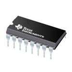
| 封装/外壳 | 16-DIP(0.300",7.62mm) |
| 封装/箱体 | PDIP-16 |
| 工作温度 | -40°C ~ 85°C |
| 工厂包装数量 | 25 |
| 开关频率 | 1000 kHz |
| 拓扑结构 | Boost, Flyback, Forward |
| 最大工作温度 | + 85 C |
| 最小工作温度 | - 40 C |
| 标准包装 | 25 |
| 电压-电源 | 8 V ~ 14.5 V |
| 类型 | Current Mode PWM Controllers |
| 系列 | UCC2806 |
| 输出数 | 2 |
| 输出电流 | 500 mA |
| 输出端数量 | 2 Output |
| 降压 | 无 |
| 隔离式 | 是 |
| 频率-最大值 | 1MHz |


- 商务部:美国ITC正式对集成电路等产品启动337调查
- 曝三星4nm工艺存在良率问题 高通将骁龙8 Gen1或转产台积电
- 太阳诱电将投资9.5亿元在常州建新厂生产MLCC 预计2023年完工
- 英特尔发布欧洲新工厂建设计划 深化IDM 2.0 战略
- 台积电先进制程称霸业界 有大客户加持明年业绩稳了
- 达到5530亿美元!SIA预计今年全球半导体销售额将创下新高
- 英特尔拟将自动驾驶子公司Mobileye上市 估值或超500亿美元
- 三星加码芯片和SET,合并消费电子和移动部门,撤换高东真等 CEO
- 三星电子宣布重大人事变动 还合并消费电子和移动部门
- 海关总署:前11个月进口集成电路产品价值2.52万亿元 增长14.8%


PDF Datasheet 数据手册内容提取
UCC1806 UCC2806 UCC3806 SLUS272F--FEBRUARY2000--REVISEDAUGUST2006 LOW-POWER, DUAL-OUTPUT, CURRENT-MODE PWM CONTROLLER FEATURES for applications ranging from off-line power suppliestobatteryoperatedportableequipment. D BiCMOSVersionofUC3846Family Dualhigh-current,MOSFETdrivingoutputsanda D 1.4-mAMaximumOperatingCurrent fast current sense loop further enhance device D 100-μAMaximumStartupCurrent versatility. D ±0.5-APeakOutputCurrent Allthebenefitsofcurrentmodecontrolincluding D 125-nsCircuitDelay simpler loop closing, voltage feed-forward, D EasierParallelability parallelabilitywithcurrentsharing,pulse-by-pulse current limiting, and push/pull symmetry D ImprovedBenefitsofCurrentModeControl correction are readily achievable with the UCC3806series. DESCRIPTION These devices are available in multiple package optionsforboththrough-holeandsurfacemount TheUCC3806familyofBiCMOSPWMcontrollers applications; and in commercial, industrial, and offersexceptionallyimprovedperformancewitha militarytemperatureranges. familiararchitecture.Withthesameblockdiagram and pinout of the popular UC3846 series, the The UCC1806 is specified for operation from UCC3806 line features increased switching --55°C to 125°C, the UCC2806 is specified for frequency capability while greatly reducing the operationfrom--40°Cto85°C,andtheUCC3806 biascurrentusedwithinthedevice.Withatypical isspecifiedforoperationfrom0°Cto70°C. startupcurrentof50μAandawelldefinedvoltage threshold for turn-on, these devices are favored SIMPLIFIED APPLICATION DIAGRAM +VOUT +VIN 15 13 UC39431 VIN VC UCC3806 2 VREF INV 6 COMP 7 8 CT 5 NI AOUT 11 1 CURLIM BOUT 14 10 SYNC SHUT 16 DOWN 9 RT CS+ 4 CS-- GND 3 12 PRODUCTION DATA information is current as of publication date. Copyright©1999--2006,TexasInstrumentsIncorporated ProductsconformtospecificationsperthetermsofTexasInstruments standardwarranty.Productionprocessingdoesnotnecessarilyinclude testingofallparameters. www.ti.com 1
UCC1806 UCC2806 UCC3806 SLUS272F--FEBRUARY2000--REVISEDAUGUST2006 Thesedeviceshavelimitedbuilt-inESDprotection.Theleadsshouldbeshortedtogetherorthedeviceplacedinconductivefoam duringstorageorhandlingtopreventelectrostaticdamagetotheMOSgates. ABSOLUTE MAXIMUM RATINGS overoperatingfree-airtemperaturerangeunlessotherwisenoted(1) UCx806 UNIT Supplyvoltage,VIN VIN,lowimpedance 15 V Supplycurrent,IIN VIN,highimpedance 25 mA Outputsupplyvoltage VC 18 V Continuoussourceorsink ±200 Gatedrive ±500 OOuuttppuuttccuurrrreenntt mmAA SYNC ±30 COMP ±10to--(self-limiting) Analoginputvoltagerange CS--,CS+,NI,INV,SHUTDOWN --0.3to(VIN+0.3) V Storagetemperature,Tstg --65to150 °C Operatingtemperature,TJ --55to150 °C Leadtemperature,Tsol,1,6mm(1/16inch)fromcasefor10seconds 300 °C (1) Stressesbeyondthoselistedunder“absolutemaximumratings”maycausepermanentdamagetothedevice.Thesearestressratingsonly, andfunctionaloperationofthedeviceattheseoranyotherconditionsbeyondthoseindicatedunder“recommendedoperatingconditions”is notimplied.Exposuretoabsolute-maximum-ratedconditionsforextendedperiodsmayaffectdevicereliability.Allvoltagesarewithrespectto GND.Currentsarepositiveintoandnegativeoutof,thespecifiedterminal. RECOMMENDED OPERATING CONDITIONS MIN NOM MAX UNIT Inputvoltage,VIN 8.0 14.5 V UCC1806 --55 125 OOppeerraattiinnggjjuunnccttiioonntteemmppeerraattuurree,,TTJJ UCC2806 --40 85 °CC UCC3806 0 70 PACKAGE DESCRIPTION D,DW,J,M,NORPWPACKAGE QORLPACKAGE (TOPVIEW) (TOPVIEW) N W O M D F LI T CURLIM 1 16 SHUTDOWN E R U R U CH N VREF 2 15 VIN V C NS VI CS-- 3 14 BOUT CS+ 4 13 VC CS-- 43 2 1 20 1918 BOUT NI 5 12 GND CS+ 5 17 VC INV 6 11 AOUT N/C 6 16 N/C COMP 7 10 SYNC NI 7 15 GND CT 8 9 RT INV 8 14 AOUT 9 10 11 12 13 P T CT C M C N/R N O Y C S N/C--Noconnection 2 www.ti.com
UCC1806 UCC2806 UCC3806 SLUS272F--FEBRUARY2000--REVISEDAUGUST2006 ORDERING INFORMATION PACKAGEDDEVICES TA=TJ DESIGNATOR TYPE OPTION QUANTITY --55°Cto125°C --40°Cto85°C 0°Cto70°C Tube 40 – UCC2806D – DD SSOOIICC--1166 Reeled 2,500 – UCC2806DTR – Tube 40 – UCC2806DW UCC3806DW DDWW SSOOIICCWW--1166 Reeled 2,000 – UCC2806DWTR UCC3806DWTR J CDIP--16 Tube 25 UCC1806J UCC2806J UCC3806J L CLCC--20 Tube 55 UCC1806L – – M SSOP--16 Reeled 2,500 – UCC2806MTR – N PDIP--16 Tube 25 – UCC2806N UCC3806N Tube 90 – UCC2806PW UCC3806PW PPWW TTSSSSOOPP--1166 Reeled 2,000 – UCC2806PWTR UCC3806PWTR Tube 46 – UCC2806Q UCC3806Q QQ PPLLCCCC--2200 Reeled 1,000 – UCC2806QTR UCC3806QTR ELECTRICAL CHARACTERISTICS VIN=12V,RT=33kΩ,CT=330pF,CBYPASSonVREF=0.01μF,--55°C<TA<125°CfortheUCC1806,--40°C<TA<85°Cforthe UCC2806,0°C<TA<70°CfortheUCC3806,andTA=TJ(unlessotherwisenoted) PARAMETER TESTCONDITIONS MIN TYP MAX UNIT REFERENCE UCC1806 5.02 5.10 5.17 VVRREEFF SSuuppppllyy,,UUVVLLOO,,ttuurrnn-oonn UCC2806 VV UCC3806 5.00 5.10 5.20 Loadregulation 0.2mA≤IOUT≤5mA 3 25 mmVV Totaloutputvariation(1)(2) Line,load,temperature --150 150 Outputnoisevoltage(2) 10Hz≤fOSC≤10kHz, TJ=25°C 70 μV Longtermstability(2) TA=125°C, 1000hours 5 25 mV Outputshortcircuit --10 --30 mA OSCILLATOR Initialaccuracy TJ=25°C 42 47 52 kHz Temperaturestability(2) T(min) ≤TA≤T(max) 2% Amplitude 2.35 V UCC1806 VCT=0V, VRT=VREF 50 125 UCC2806 0.8V≤VSYNC≤2.0V ttDELAY DDeellaayy-ttoo-oouuttppuuttttiimmee,SSYYNNCC UCC3806 VCT=0V, VRT=VREF 50 100 nnss 0.8V≤VSYNC≤2.0V www.ti.com 3
UCC1806 UCC2806 UCC3806 SLUS272F--FEBRUARY2000--REVISEDAUGUST2006 ELECTRICAL CHARACTERISTICS VIN=12V,RT=33kΩ,CT=330pF,CBYPASSonVREF=0.01μF,--55°C<TA<125°CfortheUCC1806,--40°C<TA<85°Cforthe UCC2806,0°C<TA<70°CfortheUCC3806,andTA=TJ(unlessotherwisenoted) PARAMETER TESTCONDITIONS MIN TYP MAX UNIT OSCILLATOR(continued) IDCHG Dischargecurrent TJ=25°C, VCT=2.0V 2.5 mA VOL Low-leveloutputvoltage,SYNC IOUT=1mA 0.4 VOH High-leveloutputvoltage,SYNC IOUT=--4mA 2.4 VV VIL Low-levelinputvoltage,SYNC VCT=0V, VRT=VREF 0.8 VIH High-levelinputvoltage,SYNC VCT=0V, VRT=VREF 2.0 ISYNC Inputcurrent,SYNC --1 1 μA ERRORAMPLIFIER UCC1806 5 IInnppuuttooffffsseettvvoollttaaggee UCC2806 mmVV UCC3806 10 IBIAS Inputbiascurrent --1 μA IOFSET Inputoffsetcurrent 500 nA CMR Commonmoderange(1) 0 VIN--2 V AVOL Openloopgain 1V≤VOUT≤4V 80 100 dB GBW bandwidth 1 MHz ICOMP_SINK Outputsinkcurrent VID<--20mV, VCOMP=1V 1 mA ICOMP_SRC Outputsourcecurrent VID< 20mV, VCOMP=3V --80 --120 μA VCOMP_L Low-leveloutputvoltage VID=--50mV 0.5 VV VCOMP_H High-leveloutputvoltage VID=--50mV 4.5 CURRENTSENSEAMPLIFIER A Amplifiergain(3)(4) VCS--=0V, VCURLIM=VREF 2.75 3.00 3.35 V/V Maximumdifferentialinputsignal(VCS+ VCURLIM=VNI=VREF, 1.1 V --VCS--) VINV=0V UCC1806 IInnppuuttooffffsseettvvoollttaaggee UCC2806 VCURLIM=0.5V, VCOMP=OPEN 10 30 mV UCC3806 VCURLIM=0.5V, VCOMP=OPEN 10 50 mV CMRR Commonmoderejectionratio 0V≤VCM≤(VIN--3.5V) 60 dB PSRR Powersupplyrejectionratio 56 dB IBIAS Inputbiascurrent(3) VCURLIM=0.5V, VCOMP=OPEN --1 μA Inputoffsetcurrent(3) VCURLIM=0.5V, VCOMP=OPEN 1 μA VNI=VREF, VINV=0V, Delay-to-outputtime(5) VCURLIM=2.75V, 125 175 ns (VCS+--VCS--)= 0Vto1.5Vstep CURRENTLIMITADJUST Currentlimitoffset VCS--=VCS+=0V, VCOMP=OPEN 0.4 0.5 0.6 V IBIAS Inputbiascurrent 1 Minimumlatchingcurrent 300 200 μμAA Maximumnon-latchingcurrent 200 80 (1) Linerange=10Vto15V,loadrange=0.2mAto5mA (2) Ensuredbydesign.Notproductiontested. 4 www.ti.com
UCC1806 UCC2806 UCC3806 SLUS272F--FEBRUARY2000--REVISEDAUGUST2006 ELECTRICAL CHARACTERISTICS VIN=12V,RT=33kΩ,CT=330pF,CBYPASSonVREF=0.01μF,--55°Cto125°CfortheUCC1806,--40°C<TA<85°CfortheUCC2806, 0°C<TA<70°CfortheUCC3806,andTA=TJ(unlessotherwisenoted) SHUTDOWNTERMINAL UCC1806 0.94 1.00 1.06 TThhrreesshhoollddvvoollttaaggee UCC2806 VV UCC3806 0.9 1.0 1.1 Inputvoltagerange 0 VIN tDLY Delay-to-outputtime 0V≤VSHUTDOWN≤1.3V 75 150 ns OUTPUT Outputsupplyvoltage 2.5 15.0 UUCCCC11880066 ISINK=20mA 100 300 UCC2806 ISINK=100mA 0.4 1.1 LLooww-lleevveelloouuttppuuttvvoollttaaggee ISINK=20mA 100 200 VV UUCCCC33880066 ISINK=100mA 0.4 1.1 ISRC=--20mA 11.6 11.9 HHiigghh-lleevveelloouuttppuuttvvoollttaaggee ISRC=--100mA 11.0 11.6 tRISE Risetime TJ=25°C, CLOAD=1000pF 35 65 nnss tFALL Falltime TJ=25°C, CLOAD=1000pF 35 65 UNDERVOLTAGELOCKOUT(UVLO) VSTART Startupthresholdvoltage 6.5 7.5 8.0 V Thresholdhysteresis 0.75 V ISTART Startupcurrent VIN<VSTART 50 100 μA I Operatingsupplycurrent 1.0 1.4 mA VINshuntvoltage IVIN=10mA 15.0 17.5 (1) Linerange=10Vto15V,loadrange=0.2mAto5mA (2) Ensuredbydesign.Notproductiontested. (3) ParametersmeasuredattrippointoflatchwithVNI=VREF,VINV=0V. (4) Amplifiergaindefinedas:G=deltachangeatCOMP/deltachangeforcedatCS+deltavoltageatCS+=0to1V (5) Current-senseamplifieroutputisslewratelimitedtoprovidenoiseimmunity. THERMAL RESISTANCE TABLE PACKAGE θJC θJA PACKAGETYPE DESIGNATOR (°C/W) (°C/W) D SOIC--16 35 50to120(1) DW SOICW--16 27 50to100(1) J CDIP--16 28 80to120 L CLCC--20 20 70to80 M SSOP--16 38 144to172(2) N PDIP--16 45 90(1) PW TSSOP--16 15 123to147(2) Q PLCC--20 34 43to75(1) (1) SpecifiedθJA(junctiontoambient)isfordevicesmountedto5in2FR4PCboard withoneouncecopperwherenoted.Whenresistancerangeisgiven,lowervalues arefor5in2aluminumPCboard.TestPWBwas0.062inthickandtypicallyused 0.635mmtracewidthsforpowerpackagesand1.3mmtracewidthsfornon-power packageswitha100x100milprobelandareaattheendofeachtrace. (2) Modeleddata.Ifvaluerangegivenfor θJA,thelowervalueisfor3x3inch1oz internalcoppergroundplane,andthehighervalueisfor1x1inchgroundplane.All modeldataassumesonlyonetraceforeachnon-fusedlead. www.ti.com 5
UCC1806 UCC2806 UCC3806 SLUS272F--FEBRUARY2000--REVISEDAUGUST2006 TERMINAL FUNCTIONS TERMINAL PACKAGES II//OO DDEESSCCRRIIPPTTIIOONN NAME D/DW/J/M L,Q /N/PW AOUT 11 14 OO HHiigghh-ccuurrrreennttggaatteeddrriivveeffoorrtthheeeexxtteerrnnaallMMOOSSFFEETTss BOUT 14 18 COMP 7 9 O Outputoftheerroramplifier CS-- 3 4 I Invertinginputofthe3×,differentialcurrentsenseamplifier CS+ 4 5 I Non-invertinginputofthe3×,differentialcurrentsenseamplifier CT 8 10 I Oscillatortimingcapacitorconnectionpoint Programstheprimarycurrentlimitthresholdthatdeterminslatchingorretryafteran CURLIM 1 2 I overcurrentsituation GND 12 15 -- Referencegroundandpowergroundforallfunctionsofthisdevice INV 6 8 I Invertinginputoftheerroramplifier. NI 5 7 I Non-nvertinginputoftheerroramplifier. RT 9 12 I Connectionpointfortheoscillatortimingresistor Providedforenhancedprotection.WhenSHUTDOWNisdrivenabove1V,AOUTand SHUTDOWN 16 20 I BOUTareforcedlow. SYNC 10 13 I/O AllowsprovidingexternalsynchronizationwithTTLcompatiblethresholds. VC 13 17 I InputsupplyconnectionfortheFETdriveoutputs. VIN 15 19 I Inputsupplyconnectionforthisdevice. VREF 2 3 O Referenceoutput. DETAILED PIN DESCRIPTIONS AOUTandBOUT:AOUTandBOUTprovidealternatinghighcurrentgatedrivefortheexternalMOSFETs.Duty cycle can be varied from 0% to 50% where minimum dead time is a function of CT. Both outputs use MOS transistorswitcheswithinherentanti-parallelbodydiodestoclampvoltageswingstothesupplyrails,allowing operationwithouttheuseofclampdiodes. COMP:COMPistheoutputoftheerroramplifierandtheinputofthePWMcomparator.Theerroramplifieris alowoutputimpedance,2-MHzoperationalamplifierwhichallowssinkingorsourcingofcurrentattheCOMP pin.Theerroramplifierisinternallycurrentlimited,sothatzerodutycyclecanbecommandedbyexternally forcingCOMPtoGND. CS--:CS-- istheinvertinginputofthe3×differentialcurrentsenseamplifier. CS+:CS+isthenon-invertinginputofthe3×differentialcurrentsenseamplifier. CT: CT is the oscillator timing capacitor connection point, which is charged by the current set by RT. CT is discharged to GND through a 2.5-mA current sink. This causes a linear discharge of CT to 0 V which then initiatesthenextswitchingcycle.DeadtimeoccursduringthedischargeofCT,forcingAOUTandBOUTlow. Switchingfrequency(f )anddeadtime(t )areapproximatedby: S D 1 fS=1.96×RT×CT+tD and tD=956×CT (1) 6 www.ti.com
UCC1806 UCC2806 UCC3806 SLUS272F--FEBRUARY2000--REVISEDAUGUST2006 DETAILED PIN DESCRIPTIONS (continued) CURLIM:CURLIMprogramstheprimarycurrentlimitthresholdanddetermineswhetherthedevicelatchesoff or retries after an overcurrent condition. When a shutdown signal is generated, a 200-μA current source to groundpullsdownonCURLIM.Ifthevoltageonthepinremainsabove350mVthedeviceremainslatchedand thepowermustbecycledtorestart.Ifthevoltageonthepinfallsbelow350mV,thedeviceattemptsarestart. Thevoltagethresholdistypicallysetbyaresistor dividerfromV to ground.To calculatethe currentlimit REF adjustvoltagethresholdthefollowingequationscanbeused. Currentlimitadjustlatchingmodevoltageiscalculatedinequation(2) V=VREF−(R1×300mA)>350mV 1+R1 R2 (2) Currentlimitadjustnon-latchingmodevoltageiscalculatedinequation(3) V=VREF−(R1×80mA)<350mV 1+R1 R2 (3) where D R1istheresistancefromtheVREFtoCURLIM D R2istheresistancefromCURLIMtoGND GND:GNDisthereferencegroundandpowergroundforallfunctionsofthispart.Bypassandtimingcapacitors shouldbeconnectedascloseaspossibletoGND. RT:RTistheconnectionpointfortheoscillatortimingresistor.Ithasalowimpedanceinputandisnominally at1.25V.ThecurrentthroughRTismirroredtothetimingcapacitorpin,CT.Thiscausesalinearchargingof CTfrom0Vto2.35V.Notethatthecurrentmirrorislimitedtoamaximumof100μAsoR mustbegreater T than12.5kΩ. SYNC: SYNC is a bi-directional pin, allowing or providing external synchronization with TTL compatible thresholds.InatypicalapplicationRTisconnectedthroughatimingresistortoGNDwhichallowstheinternal oscillatortofreerun.InthismodeSYNCoutputsaTTLcompatiblepulseduringtheoscillatordeadtime(when CTisbeingdischarged).IfRTisforcedabove4.4V,SYNCactsasaninputwithTTLcompatiblethresholds and the internaloscillator is disabled.When SYNCis high,greater than2Vtheoutputs areheld activelow. WhenSYNCreturnslow,theoutputsmaybehighuntiltheon--timeisterminatedbythenormalpeakcurrent signal, a fault seen at SHUTDOWN or the next high assertion of SYNC. Multiple UCC3806s can be synchronizedbyasinglemasterUCC3806orexternalclock. VC:VCistheinputsupplyconnectionfortheFETdriveoutputsandhasaninputrangefrom2.5Vto15V.VC shouldbecapacitivelybypassedforproperoperation. VIN:VINistheinputsupplyconnectionforthisdevice.TheUCC1806hasamaximumstartupthresholdof8V andinternallylimitedbymeansofa15Vshuntregulator.Theshuntedsupplycurrentmustbelimitedto25mA. Forproperoperation,VINmustbebypassedtoGNDwithatleasta0.01-μFceramiccapacitor VREF:VREFisa5.1V±1%trimmedreferenceoutputwitha5mAmaximumavailablecurrent.VREFmustbe bypassedtoGNDwithatleasta0.1-μFceramiccapacitorforproperoperation. www.ti.com 7
UCC1806 UCC2806 UCC3806 SLUS272F--FEBRUARY2000--REVISEDAUGUST2006 FUNCTIONAL BLOCK DIAGRAM SYNC 10 13 VC 4.4V -- 1.5V -- RT 9 + + 11 AOUT OSC Q CT 8 LO 14 BOUT R T QB Comparator CS-- 3 --3X + S1 QB 12 GND + -- S2 CS+ 4 Shutdown -- 0.5V 120μA Lockout + NI 5 1 CURLIM + EA -- INV 6 -- R S1 + 0.35V COMP 7 Q Q S 7.0V + S2R 200μA +-- 1.0V 16 DSOHWUTN VIN 15 -- S 200kΩ Q CurrentLimit + R Restart 7.5V -- UVLO 15V 5.1V 4.25V + 2 VREF Reference -- ReferenceLow Regulator UDG--99035 8 www.ti.com
UCC1806 UCC2806 UCC3806 SLUS272F--FEBRUARY2000--REVISEDAUGUST2006 TYPICAL APPLICATION DIAGRAM UDG--99036 TYPICAL CHARACTERISTICS Designequationsforoscillatoraredescribedinthefollowingequations. 1 fOSC=tRAMP+tFALL (4) tRAMP=1.92×RT×CT (5) tFALL= 2.4×CT 1.25 0.002− R T (6) tDEAD=tFALL (7) www.ti.com 9
UCC1806 UCC2806 UCC3806 SLUS272F--FEBRUARY2000--REVISEDAUGUST2006 TYPICAL CHARACTERISTICS OSCILLATORFREQUENCY vs ERRORAMPLIFIERGAINANDPHASE JUNCTIONTEMPERATURE vs 60 FREQUENCY 80 180 58 Hz 56 k 60 135 -- 54 y c n e Phase u 52 ° q ain--dB 40 90 Phase-- atorFre 50 G 20 45 cill 48 s O 46 -- C OS 44 0 Gain 0 f 42 --20 --45 40 1k 10k 100k 1M 10M --55 --25 0 25 50 75 100 125 fOSC--OscillatorFrequency--Hz TJ--JunctionTemperature--°C Figure1. Figure2. 10 www.ti.com
UCC1806 UCC2806 UCC3806 SLUS272F--FEBRUARY2000--REVISEDAUGUST2006 OSCILLATORFREQUENCY vs TIMINGRESISTANCE 1M CT=220pF z H k -- cy CT=100pF en 100k CT=47pF u q e r F r o at cill s O 10k --C CT=330pF S fO CT=470pF CT=1.0nF 0 CT=2.2nF 10k 100k 1M RT--TimingResistance--Ω Figure3. REVISION HISTORY DATE REVISION DESCRIPTION 3/11/05 SLUS272D(Rev.D) UpdatedEquation2and3toremovex3factor. Adjustedthefactorsoftheswitchingfrequency,Equation1andmodifiedthetypical 5/3/05 SLUS272E(Rev.E) dischargecurrentfrom2.0mAto2.5mA. www.ti.com 11
PACKAGE OPTION ADDENDUM www.ti.com 16-Oct-2009 PACKAGING INFORMATION OrderableDevice Status(1) Package Package Pins Package EcoPlan(2) Lead/BallFinish MSLPeakTemp(3) Type Drawing Qty 5962-9457501MEA ACTIVE CDIP J 16 1 TBD A42 N/AforPkgType 5962-9457501Q2A ACTIVE LCCC FK 20 1 TBD POST-PLATE N/AforPkgType UCC1806J ACTIVE CDIP J 16 1 TBD A42 N/AforPkgType UCC1806J883B ACTIVE CDIP J 16 1 TBD A42 N/AforPkgType UCC1806L ACTIVE LCCC FK 20 1 TBD POST-PLATE N/AforPkgType UCC1806L883B ACTIVE LCCC FK 20 1 TBD POST-PLATE N/AforPkgType UCC2806D ACTIVE SOIC D 16 40 Green(RoHS& CUNIPDAU Level-2-260C-1YEAR noSb/Br) UCC2806DG4 ACTIVE SOIC D 16 40 Green(RoHS& CUNIPDAU Level-2-260C-1YEAR noSb/Br) UCC2806DTR ACTIVE SOIC D 16 2500 Green(RoHS& CUNIPDAU Level-2-260C-1YEAR noSb/Br) UCC2806DTRG4 ACTIVE SOIC D 16 2500 Green(RoHS& CUNIPDAU Level-2-260C-1YEAR noSb/Br) UCC2806DW ACTIVE SOIC DW 16 40 Green(RoHS& CUNIPDAU Level-2-260C-1YEAR noSb/Br) UCC2806DWG4 ACTIVE SOIC DW 16 40 Green(RoHS& CUNIPDAU Level-2-260C-1YEAR noSb/Br) UCC2806DWTR ACTIVE SOIC DW 16 2000 Green(RoHS& CUNIPDAU Level-2-260C-1YEAR noSb/Br) UCC2806DWTRG4 ACTIVE SOIC DW 16 2000 Green(RoHS& CUNIPDAU Level-2-260C-1YEAR noSb/Br) UCC2806J ACTIVE CDIP J 16 1 TBD A42 N/AforPkgType UCC2806M ACTIVE SSOP/ DBQ 16 75 Green(RoHS& CUNIPDAU Level-2-260C-1YEAR QSOP noSb/Br) UCC2806MG4 ACTIVE SSOP/ DBQ 16 75 Green(RoHS& CUNIPDAU Level-2-260C-1YEAR QSOP noSb/Br) UCC2806MTR ACTIVE SSOP/ DBQ 16 2500 Green(RoHS& CUNIPDAU Level-2-260C-1YEAR QSOP noSb/Br) UCC2806MTRG4 ACTIVE SSOP/ DBQ 16 2500 Green(RoHS& CUNIPDAU Level-2-260C-1YEAR QSOP noSb/Br) UCC2806N ACTIVE PDIP N 16 25 Green(RoHS& CUNIPDAU N/AforPkgType noSb/Br) UCC2806NG4 ACTIVE PDIP N 16 25 Green(RoHS& CUNIPDAU N/AforPkgType noSb/Br) UCC2806PW ACTIVE TSSOP PW 16 90 Green(RoHS& CUNIPDAU Level-2-260C-1YEAR noSb/Br) UCC2806PWG4 ACTIVE TSSOP PW 16 90 Green(RoHS& CUNIPDAU Level-2-260C-1YEAR noSb/Br) UCC2806PWTR ACTIVE TSSOP PW 16 2000 Green(RoHS& CUNIPDAU Level-2-260C-1YEAR noSb/Br) UCC2806PWTRG4 ACTIVE TSSOP PW 16 2000 Green(RoHS& CUNIPDAU Level-2-260C-1YEAR noSb/Br) UCC2806Q ACTIVE PLCC FN 20 46 Green(RoHS& CUSN Level-2-260C-1YEAR noSb/Br) UCC2806QG3 ACTIVE PLCC FN 20 46 Green(RoHS& CUSN Level-2-260C-1YEAR noSb/Br) UCC3806DW ACTIVE SOIC DW 16 40 Green(RoHS& CUNIPDAU Level-2-260C-1YEAR Addendum-Page1
PACKAGE OPTION ADDENDUM www.ti.com 16-Oct-2009 OrderableDevice Status(1) Package Package Pins Package EcoPlan(2) Lead/BallFinish MSLPeakTemp(3) Type Drawing Qty noSb/Br) UCC3806DWG4 ACTIVE SOIC DW 16 40 Green(RoHS& CUNIPDAU Level-2-260C-1YEAR noSb/Br) UCC3806DWTR ACTIVE SOIC DW 16 2000 Green(RoHS& CUNIPDAU Level-2-260C-1YEAR noSb/Br) UCC3806DWTRG4 ACTIVE SOIC DW 16 2000 Green(RoHS& CUNIPDAU Level-2-260C-1YEAR noSb/Br) UCC3806J ACTIVE CDIP J 16 1 TBD A42 N/AforPkgType UCC3806N ACTIVE PDIP N 16 25 Green(RoHS& CUNIPDAU N/AforPkgType noSb/Br) UCC3806NG4 ACTIVE PDIP N 16 25 Green(RoHS& CUNIPDAU N/AforPkgType noSb/Br) UCC3806PW ACTIVE TSSOP PW 16 90 Green(RoHS& CUNIPDAU Level-2-260C-1YEAR noSb/Br) UCC3806PWG4 ACTIVE TSSOP PW 16 90 Green(RoHS& CUNIPDAU Level-2-260C-1YEAR noSb/Br) UCC3806Q ACTIVE PLCC FN 20 46 Green(RoHS& CUSN Level-2-260C-1YEAR noSb/Br) UCC3806QG3 ACTIVE PLCC FN 20 46 Green(RoHS& CUSN Level-2-260C-1YEAR noSb/Br) UCC3806QTR ACTIVE PLCC FN 20 1000 Green(RoHS& CUSN Level-2-260C-1YEAR noSb/Br) UCC3806QTRG3 ACTIVE PLCC FN 20 1000 Green(RoHS& CUSN Level-2-260C-1YEAR noSb/Br) (1)Themarketingstatusvaluesaredefinedasfollows: ACTIVE:Productdevicerecommendedfornewdesigns. LIFEBUY:TIhasannouncedthatthedevicewillbediscontinued,andalifetime-buyperiodisineffect. NRND:Notrecommendedfornewdesigns.Deviceisinproductiontosupportexistingcustomers,butTIdoesnotrecommendusingthispartin anewdesign. PREVIEW:Devicehasbeenannouncedbutisnotinproduction.Samplesmayormaynotbeavailable. OBSOLETE:TIhasdiscontinuedtheproductionofthedevice. (2)EcoPlan-Theplannedeco-friendlyclassification:Pb-Free(RoHS),Pb-Free(RoHSExempt),orGreen(RoHS&noSb/Br)-pleasecheck http://www.ti.com/productcontentforthelatestavailabilityinformationandadditionalproductcontentdetails. TBD:ThePb-Free/Greenconversionplanhasnotbeendefined. Pb-Free(RoHS):TI'sterms"Lead-Free"or"Pb-Free"meansemiconductorproductsthatarecompatiblewiththecurrentRoHSrequirements forall6substances,includingtherequirementthatleadnotexceed0.1%byweightinhomogeneousmaterials.Wheredesignedtobesoldered athightemperatures,TIPb-Freeproductsaresuitableforuseinspecifiedlead-freeprocesses. Pb-Free(RoHSExempt):ThiscomponenthasaRoHSexemptionforeither1)lead-basedflip-chipsolderbumpsusedbetweenthedieand package, or 2) lead-based die adhesive used between the die and leadframe. The component is otherwise considered Pb-Free (RoHS compatible)asdefinedabove. Green(RoHS&noSb/Br):TIdefines"Green"tomeanPb-Free(RoHScompatible),andfreeofBromine(Br)andAntimony(Sb)basedflame retardants(BrorSbdonotexceed0.1%byweightinhomogeneousmaterial) (3) MSL, Peak Temp. -- The Moisture Sensitivity Level rating according to the JEDEC industry standard classifications, and peak solder temperature. Important Information and Disclaimer:The information provided on this page represents TI's knowledge and belief as of the date that it is provided. TI bases its knowledge and belief on information provided by third parties, and makes no representation or warranty as to the accuracy of such information. Efforts are underway to better integrate information from third parties. TI has taken and continues to take reasonable steps to provide representative and accurate information but may not have conducted destructive testing or chemical analysis on incomingmaterialsandchemicals.TIandTIsuppliersconsidercertaininformationtobeproprietary,andthusCASnumbersandotherlimited informationmaynotbeavailableforrelease. Addendum-Page2
PACKAGE OPTION ADDENDUM www.ti.com 16-Oct-2009 InnoeventshallTI'sliabilityarisingoutofsuchinformationexceedthetotalpurchasepriceoftheTIpart(s)atissueinthisdocumentsoldbyTI toCustomeronanannualbasis. OTHERQUALIFIEDVERSIONSOFUCC1806,UCC2806,UCC2806M,UCC3806,UCC3806M: •Space:UCC1806-SP NOTE:QualifiedVersionDefinitions: •Space-Radiationtolerant,ceramicpackagingandqualifiedforuseinSpace-basedapplication Addendum-Page3
PACKAGE OPTION ADDENDUM www.ti.com 6-Feb-2020 PACKAGING INFORMATION Orderable Device Status Package Type Package Pins Package Eco Plan Lead/Ball Finish MSL Peak Temp Op Temp (°C) Device Marking Samples (1) Drawing Qty (2) (6) (3) (4/5) 5962-9457501MEA ACTIVE CDIP J 16 1 TBD Call TI N / A for Pkg Type -55 to 125 5962-9457501ME A UCC1806J/883B 5962-9457501Q2A ACTIVE LCCC FK 20 1 TBD POST-PLATE N / A for Pkg Type -55 to 125 5962- 9457501Q2A UCC1806L/ 883B 5962-9457501V2A ACTIVE LCCC FK 20 1 TBD POST-PLATE N / A for Pkg Type -55 to 125 5962- 9457501V2A UCC1806L QMLV 5962-9457501VEA ACTIVE CDIP J 16 1 TBD Call TI N / A for Pkg Type -55 to 125 5962-9457501VE A UCC1806JQMLV UCC1806J ACTIVE CDIP J 16 1 TBD Call TI N / A for Pkg Type -55 to 125 UCC1806J UCC1806J883B ACTIVE CDIP J 16 1 TBD Call TI N / A for Pkg Type -55 to 125 5962-9457501ME A UCC1806J/883B UCC1806L ACTIVE LCCC FK 20 1 TBD POST-PLATE N / A for Pkg Type -55 to 125 UCC1806L UCC1806L883B ACTIVE LCCC FK 20 1 TBD POST-PLATE N / A for Pkg Type -55 to 125 5962- 9457501Q2A UCC1806L/ 883B UCC2806D ACTIVE SOIC D 16 40 Green (RoHS NIPDAU Level-2-260C-1 YEAR -40 to 85 UCC2806D & no Sb/Br) UCC2806DTR ACTIVE SOIC D 16 2500 Green (RoHS NIPDAU Level-2-260C-1 YEAR -40 to 85 UCC2806D & no Sb/Br) UCC2806DW ACTIVE SOIC DW 16 40 Green (RoHS NIPDAU Level-2-260C-1 YEAR -40 to 85 UCC2806DW & no Sb/Br) UCC2806DWG4 ACTIVE SOIC DW 16 40 Green (RoHS NIPDAU Level-2-260C-1 YEAR -40 to 85 UCC2806DW & no Sb/Br) UCC2806DWTR ACTIVE SOIC DW 16 2000 Green (RoHS NIPDAU Level-2-260C-1 YEAR -40 to 85 UCC2806DW & no Sb/Br) Addendum-Page 1
PACKAGE OPTION ADDENDUM www.ti.com 6-Feb-2020 Orderable Device Status Package Type Package Pins Package Eco Plan Lead/Ball Finish MSL Peak Temp Op Temp (°C) Device Marking Samples (1) Drawing Qty (2) (6) (3) (4/5) UCC2806DWTRG4 ACTIVE SOIC DW 16 2000 Green (RoHS NIPDAU Level-2-260C-1 YEAR -40 to 85 UCC2806DW & no Sb/Br) UCC2806J ACTIVE CDIP J 16 1 TBD Call TI N / A for Pkg Type -40 to 85 UCC2806J UCC2806M ACTIVE SSOP DBQ 16 75 Green (RoHS NIPDAU Level-2-260C-1 YEAR -40 to 85 UCC2806M & no Sb/Br) UCC2806MTR ACTIVE SSOP DBQ 16 2500 Green (RoHS NIPDAU Level-2-260C-1 YEAR -40 to 85 UCC2806M & no Sb/Br) UCC2806N ACTIVE PDIP N 16 25 Green (RoHS NIPDAU N / A for Pkg Type -40 to 85 UCC2806N & no Sb/Br) UCC2806PW ACTIVE TSSOP PW 16 90 Green (RoHS NIPDAU Level-2-260C-1 YEAR -40 to 85 2806 & no Sb/Br) UCC2806PWTR ACTIVE TSSOP PW 16 2000 Green (RoHS NIPDAU Level-2-260C-1 YEAR -40 to 85 2806 & no Sb/Br) UCC2806PWTRG4 ACTIVE TSSOP PW 16 2000 Green (RoHS NIPDAU Level-2-260C-1 YEAR -40 to 85 2806 & no Sb/Br) UCC3806DW ACTIVE SOIC DW 16 40 Green (RoHS NIPDAU Level-2-260C-1 YEAR 0 to 70 UCC3806DW & no Sb/Br) UCC3806DWG4 ACTIVE SOIC DW 16 40 Green (RoHS NIPDAU Level-2-260C-1 YEAR 0 to 70 UCC3806DW & no Sb/Br) UCC3806DWTR ACTIVE SOIC DW 16 2000 Green (RoHS NIPDAU Level-2-260C-1 YEAR 0 to 70 UCC3806DW & no Sb/Br) UCC3806J ACTIVE CDIP J 16 1 TBD Call TI N / A for Pkg Type 0 to 70 UCC3806J UCC3806N ACTIVE PDIP N 16 25 Green (RoHS NIPDAU N / A for Pkg Type 0 to 70 UCC3806N & no Sb/Br) UCC3806NG4 ACTIVE PDIP N 16 25 Green (RoHS NIPDAU N / A for Pkg Type 0 to 70 UCC3806N & no Sb/Br) UCC3806PW ACTIVE TSSOP PW 16 90 Green (RoHS NIPDAU Level-2-260C-1 YEAR 3806 & no Sb/Br) (1) The marketing status values are defined as follows: ACTIVE: Product device recommended for new designs. LIFEBUY: TI has announced that the device will be discontinued, and a lifetime-buy period is in effect. NRND: Not recommended for new designs. Device is in production to support existing customers, but TI does not recommend using this part in a new design. PREVIEW: Device has been announced but is not in production. Samples may or may not be available. OBSOLETE: TI has discontinued the production of the device. Addendum-Page 2
PACKAGE OPTION ADDENDUM www.ti.com 6-Feb-2020 (2) RoHS: TI defines "RoHS" to mean semiconductor products that are compliant with the current EU RoHS requirements for all 10 RoHS substances, including the requirement that RoHS substance do not exceed 0.1% by weight in homogeneous materials. Where designed to be soldered at high temperatures, "RoHS" products are suitable for use in specified lead-free processes. TI may reference these types of products as "Pb-Free". RoHS Exempt: TI defines "RoHS Exempt" to mean products that contain lead but are compliant with EU RoHS pursuant to a specific EU RoHS exemption. Green: TI defines "Green" to mean the content of Chlorine (Cl) and Bromine (Br) based flame retardants meet JS709B low halogen requirements of <=1000ppm threshold. Antimony trioxide based flame retardants must also meet the <=1000ppm threshold requirement. (3) MSL, Peak Temp. - The Moisture Sensitivity Level rating according to the JEDEC industry standard classifications, and peak solder temperature. (4) There may be additional marking, which relates to the logo, the lot trace code information, or the environmental category on the device. (5) Multiple Device Markings will be inside parentheses. Only one Device Marking contained in parentheses and separated by a "~" will appear on a device. If a line is indented then it is a continuation of the previous line and the two combined represent the entire Device Marking for that device. (6) Lead/Ball Finish - Orderable Devices may have multiple material finish options. Finish options are separated by a vertical ruled line. Lead/Ball Finish values may wrap to two lines if the finish value exceeds the maximum column width. Important Information and Disclaimer:The information provided on this page represents TI's knowledge and belief as of the date that it is provided. TI bases its knowledge and belief on information provided by third parties, and makes no representation or warranty as to the accuracy of such information. Efforts are underway to better integrate information from third parties. TI has taken and continues to take reasonable steps to provide representative and accurate information but may not have conducted destructive testing or chemical analysis on incoming materials and chemicals. TI and TI suppliers consider certain information to be proprietary, and thus CAS numbers and other limited information may not be available for release. In no event shall TI's liability arising out of such information exceed the total purchase price of the TI part(s) at issue in this document sold by TI to Customer on an annual basis. OTHER QUALIFIED VERSIONS OF UCC1806, UCC1806-SP, UCC2806, UCC2806M, UCC3806, UCC3806M : •Catalog: UCC3806, UCC1806, UCC2806, UCC3806M, UCC3806 •Military: UCC2806M, UCC1806, UCC1806 •Space: UCC1806-SP NOTE: Qualified Version Definitions: •Catalog - TI's standard catalog product •Military - QML certified for Military and Defense Applications Addendum-Page 3
PACKAGE OPTION ADDENDUM www.ti.com 6-Feb-2020 •Space - Radiation tolerant, ceramic packaging and qualified for use in Space-based application Addendum-Page 4
PACKAGE MATERIALS INFORMATION www.ti.com 15-Jan-2014 TAPE AND REEL INFORMATION *Alldimensionsarenominal Device Package Package Pins SPQ Reel Reel A0 B0 K0 P1 W Pin1 Type Drawing Diameter Width (mm) (mm) (mm) (mm) (mm) Quadrant (mm) W1(mm) UCC2806DTR SOIC D 16 2500 330.0 16.4 6.5 10.3 2.1 8.0 16.0 Q1 UCC2806DWTR SOIC DW 16 2000 330.0 16.4 10.75 10.7 2.7 12.0 16.0 Q1 UCC2806MTR SSOP DBQ 16 2500 330.0 12.4 6.4 5.2 2.1 8.0 12.0 Q1 UCC2806PWTR TSSOP PW 16 2000 330.0 12.4 6.9 5.6 1.6 8.0 12.0 Q1 UCC3806DWTR SOIC DW 16 2000 330.0 16.4 10.75 10.7 2.7 12.0 16.0 Q1 PackMaterials-Page1
PACKAGE MATERIALS INFORMATION www.ti.com 15-Jan-2014 *Alldimensionsarenominal Device PackageType PackageDrawing Pins SPQ Length(mm) Width(mm) Height(mm) UCC2806DTR SOIC D 16 2500 367.0 367.0 38.0 UCC2806DWTR SOIC DW 16 2000 367.0 367.0 38.0 UCC2806MTR SSOP DBQ 16 2500 367.0 367.0 35.0 UCC2806PWTR TSSOP PW 16 2000 367.0 367.0 35.0 UCC3806DWTR SOIC DW 16 2000 367.0 367.0 38.0 PackMaterials-Page2
None
None
None
PACKAGE OUTLINE PW0016A TSSOP - 1.2 mm max height SCALE 2.500 SMALL OUTLINE PACKAGE SEATING PLANE C 6.6 TYP 6.2 A 0.1 C PIN 1 INDEX AREA 14X 0.65 16 1 2X 5.1 4.55 4.9 NOTE 3 8 9 0.30 B 4.5 16X 0.19 1.2 MAX 4.3 0.1 C A B NOTE 4 (0.15) TYP SEE DETAIL A 0.25 GAGE PLANE 0.15 0.05 0.75 0.50 0 -8 DETA 20AIL A TYPICAL 4220204/A 02/2017 NOTES: 1. All linear dimensions are in millimeters. Any dimensions in parenthesis are for reference only. Dimensioning and tolerancing per ASME Y14.5M. 2. This drawing is subject to change without notice. 3. This dimension does not include mold flash, protrusions, or gate burrs. Mold flash, protrusions, or gate burrs shall not exceed 0.15 mm per side. 4. This dimension does not include interlead flash. Interlead flash shall not exceed 0.25 mm per side. 5. Reference JEDEC registration MO-153. www.ti.com
EXAMPLE BOARD LAYOUT PW0016A TSSOP - 1.2 mm max height SMALL OUTLINE PACKAGE 16X (1.5) SYMM (R0.05) TYP 1 16X (0.45) 16 SYMM 14X (0.65) 8 9 (5.8) LAND PATTERN EXAMPLE EXPOSED METAL SHOWN SCALE: 10X SOLDER MASK METAL UNDER SOLDER MASK OPENING METAL SOLDER MASK OPENING EXPOSED METAL EXPOSED METAL 0.05 MAX 0.05 MIN ALL AROUND ALL AROUND NON-SOLDER MASK SOLDER MASK DEFINED DEFINED (PREFERRED) SOLDE15.000R MASK DETAILS 4220204/A 02/2017 NOTES: (continued) 6. Publication IPC-7351 may have alternate designs. 7. Solder mask tolerances between and around signal pads can vary based on board fabrication site. www.ti.com
EXAMPLE STENCIL DESIGN PW0016A TSSOP - 1.2 mm max height SMALL OUTLINE PACKAGE 16X (1.5) SYMM (R0.05) TYP 1 16X (0.45) 16 SYMM 14X (0.65) 8 9 (5.8) SOLDER PASTE EXAMPLE BASED ON 0.125 mm THICK STENCIL SCALE: 10X 4220204/A 02/2017 NOTES: (continued) 8. Laser cutting apertures with trapezoidal walls and rounded corners may offer better paste release. IPC-7525 may have alternate design recommendations. 9. Board assembly site may have different recommendations for stencil design. www.ti.com
GENERIC PACKAGE VIEW DW 16 SOIC - 2.65 mm max height 7.5 x 10.3, 1.27 mm pitch SMALL OUTLINE INTEGRATED CIRCUIT This image is a representation of the package family, actual package may vary. Refer to the product data sheet for package details. 4224780/A www.ti.com
PACKAGE OUTLINE DW0016A SOIC - 2.65 mm max height SCALE 1.500 SOIC C 10.63 SEATING PLANE TYP 9.97 A PIN 1 ID 0.1 C AREA 14X 1.27 16 1 10.5 2X 10.1 8.89 NOTE 3 8 9 0.51 16X 0.31 7.6 B 7.4 0.25 C A B 2.65 MAX NOTE 4 0.33 TYP 0.10 SEE DETAIL A 0.25 GAGE PLANE 0.3 0 - 8 0.1 1.27 0.40 DETAIL A (1.4) TYPICAL 4220721/A 07/2016 NOTES: 1. All linear dimensions are in millimeters. Dimensions in parenthesis are for reference only. Dimensioning and tolerancing per ASME Y14.5M. 2. This drawing is subject to change without notice. 3. This dimension does not include mold flash, protrusions, or gate burrs. Mold flash, protrusions, or gate burrs shall not exceed 0.15 mm, per side. 4. This dimension does not include interlead flash. Interlead flash shall not exceed 0.25 mm, per side. 5. Reference JEDEC registration MS-013. www.ti.com
EXAMPLE BOARD LAYOUT DW0016A SOIC - 2.65 mm max height SOIC 16X (2) SEE SYMM DETAILS 1 16 16X (0.6) SYMM 14X (1.27) 8 9 R0.05 TYP (9.3) LAND PATTERN EXAMPLE SCALE:7X METAL SOLDER MASK SOLDER MASK METAL OPENING OPENING 0.07 MAX 0.07 MIN ALL AROUND ALL AROUND NON SOLDER MASK SOLDER MASK DEFINED DEFINED SOLDER MASK DETAILS 4220721/A 07/2016 NOTES: (continued) 6. Publication IPC-7351 may have alternate designs. 7. Solder mask tolerances between and around signal pads can vary based on board fabrication site. www.ti.com
EXAMPLE STENCIL DESIGN DW0016A SOIC - 2.65 mm max height SOIC 16X (2) SYMM 1 16 16X (0.6) SYMM 14X (1.27) 8 9 R0.05 TYP (9.3) SOLDER PASTE EXAMPLE BASED ON 0.125 mm THICK STENCIL SCALE:7X 4220721/A 07/2016 NOTES: (continued) 8. Laser cutting apertures with trapezoidal walls and rounded corners may offer better paste release. IPC-7525 may have alternate design recommendations. 9. Board assembly site may have different recommendations for stencil design. www.ti.com
None
None
PACKAGE OUTLINE DBQ0016A SSOP - 1.75 mm max height SCALE 2.800 SHRINK SMALL-OUTLINE PACKAGE C SEATING PLANE .228-.244 TYP [5.80-6.19] .004 [0.1] C A PIN 1 ID AREA 14X .0250 [0.635] 16 1 2X .189-.197 .175 [4.81-5.00] [4.45] NOTE 3 8 9 16X .008-.012 B .150-.157 [0.21-0.30] .069 MAX [3.81-3.98] [1.75] NOTE 4 .007 [0.17] C A B .005-.010 TYP [0.13-0.25] SEE DETAIL A .010 [0.25] GAGE PLANE .004-.010 0 - 8 [0.11-0.25] .016-.035 [0.41-0.88] DETAIL A (.041 ) TYPICAL [1.04] 4214846/A 03/2014 NOTES: 1. Linear dimensions are in inches [millimeters]. Dimensions in parenthesis are for reference only. Controlling dimensions are in inches. Dimensioning and tolerancing per ASME Y14.5M. 2. This drawing is subject to change without notice. 3. This dimension does not include mold flash, protrusions, or gate burrs. Mold flash, protrusions, or gate burrs shall not exceed .006 inch, per side. 4. This dimension does not include interlead flash. 5. Reference JEDEC registration MO-137, variation AB. www.ti.com
EXAMPLE BOARD LAYOUT DBQ0016A SSOP - 1.75 mm max height SHRINK SMALL-OUTLINE PACKAGE 16X (.063) [1.6] SYMM SEE DETAILS 1 16 16X (.016 ) [0.41] 14X (.0250 ) [0.635] 8 9 (.213) [5.4] LAND PATTERN EXAMPLE SCALE:8X SOLDER MASK SOLDER MASK METAL OPENING OPENING METAL .002 MAX .002 MIN [0.05] [0.05] ALL AROUND ALL AROUND NON SOLDER MASK SOLDER MASK DEFINED DEFINED SOLDER MASK DETAILS 4214846/A 03/2014 NOTES: (continued) 6. Publication IPC-7351 may have alternate designs. 7. Solder mask tolerances between and around signal pads can vary based on board fabrication site. www.ti.com
EXAMPLE STENCIL DESIGN DBQ0016A SSOP - 1.75 mm max height SHRINK SMALL-OUTLINE PACKAGE 16X (.063) [1.6] SYMM 1 16 16X (.016 ) [0.41] SYMM 14X (.0250 ) [0.635] 8 9 (.213) [5.4] SOLDER PASTE EXAMPLE BASED ON .005 INCH [0.127 MM] THICK STENCIL SCALE:8X 4214846/A 03/2014 NOTES: (continued) 8. Laser cutting apertures with trapezoidal walls and rounded corners may offer better paste release. IPC-7525 may have alternate design recommendations. 9. Board assembly site may have different recommendations for stencil design. www.ti.com
None
IMPORTANTNOTICEANDDISCLAIMER TI PROVIDES TECHNICAL AND RELIABILITY DATA (INCLUDING DATASHEETS), DESIGN RESOURCES (INCLUDING REFERENCE DESIGNS), APPLICATION OR OTHER DESIGN ADVICE, WEB TOOLS, SAFETY INFORMATION, AND OTHER RESOURCES “AS IS” AND WITH ALL FAULTS, AND DISCLAIMS ALL WARRANTIES, EXPRESS AND IMPLIED, INCLUDING WITHOUT LIMITATION ANY IMPLIED WARRANTIES OF MERCHANTABILITY, FITNESS FOR A PARTICULAR PURPOSE OR NON-INFRINGEMENT OF THIRD PARTY INTELLECTUAL PROPERTY RIGHTS. These resources are intended for skilled developers designing with TI products. You are solely responsible for (1) selecting the appropriate TI products for your application, (2) designing, validating and testing your application, and (3) ensuring your application meets applicable standards, and any other safety, security, or other requirements. These resources are subject to change without notice. TI grants you permission to use these resources only for development of an application that uses the TI products described in the resource. Other reproduction and display of these resources is prohibited. No license is granted to any other TI intellectual property right or to any third party intellectual property right. TI disclaims responsibility for, and you will fully indemnify TI and its representatives against, any claims, damages, costs, losses, and liabilities arising out of your use of these resources. TI’s products are provided subject to TI’s Terms of Sale (www.ti.com/legal/termsofsale.html) or other applicable terms available either on ti.com or provided in conjunction with such TI products. TI’s provision of these resources does not expand or otherwise alter TI’s applicable warranties or warranty disclaimers for TI products. Mailing Address: Texas Instruments, Post Office Box 655303, Dallas, Texas 75265 Copyright © 2020, Texas Instruments Incorporated