ICGOO在线商城 > 集成电路(IC) > PMIC - 栅极驱动器 > UCC27324P
 Datasheet下载
- 型号: UCC27324P
- 制造商: Texas Instruments
- 库位|库存: xxxx|xxxx
- 要求:
| 数量阶梯 | 香港交货 | 国内含税 |
| +xxxx | $xxxx | ¥xxxx |
查看当月历史价格
查看今年历史价格
UCC27324P产品简介:
ICGOO电子元器件商城为您提供UCC27324P由Texas Instruments设计生产,在icgoo商城现货销售,并且可以通过原厂、代理商等渠道进行代购。 UCC27324P价格参考。Texas InstrumentsUCC27324P封装/规格:PMIC - 栅极驱动器, Low-Side Gate Driver IC Non-Inverting 8-PDIP。您可以下载UCC27324P参考资料、Datasheet数据手册功能说明书,资料中有UCC27324P 详细功能的应用电路图电压和使用方法及教程。
Texas Instruments(德州仪器)的UCC27324P是一款高性能的PMIC(电源管理集成电路)栅极驱动器,广泛应用于需要高效开关和快速响应的场景。以下是其主要应用场景:

1. 电机驱动:UCC27324P适用于无刷直流电机(BLDC)和其他类型的电机控制。它能够快速驱动MOSFET或IGBT,提供高效的功率转换,从而实现电机的精确控制。

2. DC-DC转换器:在开关模式电源(SMPS)中,该器件可以用于驱动功率MOSFET或IGBT,提高效率并减少能量损耗。它的高速性能有助于实现更小、更轻的电源解决方案。

3. 逆变器应用:在太阳能逆变器和UPS系统中,UCC27324P能够驱动高频开关器件,确保系统的稳定性和效率。它支持高侧和低侧驱动,适用于全桥和半桥拓扑。

4. LED照明:在大功率LED驱动电路中,该器件可驱动开关晶体管以调节电流,确保LED亮度一致且节能。其低延迟特性有助于实现快速调光和调色。

5. 消费电子设备:如笔记本电脑适配器、智能手机快充模块等,UCC27324P可用于驱动功率级元件,提供快速充电功能的同时保持系统稳定性。

6. 工业自动化:在工业控制领域,这款栅极驱动器可用于伺服驱动器、机器人控制系统等,提供快速响应和高可靠性。

UCC27324P以其高驱动能力、低传播延迟和宽输入电压范围而著称,非常适合需要高效率和高可靠性的电力电子应用。
| 参数 | 数值 |
| 产品目录 | 集成电路 (IC)半导体 |
| 描述 | IC MOSFET DRVR DUAL HS 4A 8-DIP门驱动器 Dual 4 A Peak High Speed Low-Side |
| 产品分类 | PMIC - MOSFET,电桥驱动器 - 外部开关集成电路 - IC |
| 品牌 | Texas Instruments |
| 产品手册 | |
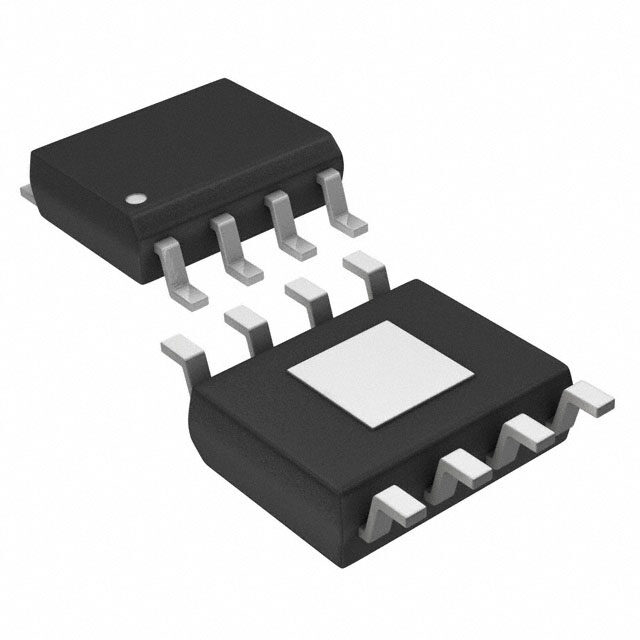
| 产品图片 |
|
| rohs | 符合RoHS无铅 / 符合限制有害物质指令(RoHS)规范要求 |
| 产品系列 | 电源管理 IC,门驱动器,Texas Instruments UCC27324P- |
| 数据手册 | |
| 产品型号 | UCC27324P |
| 上升时间 | 23 ns |
| 下降时间 | 23 ns |
| 产品目录页面 | |
| 产品种类 | 门驱动器 |
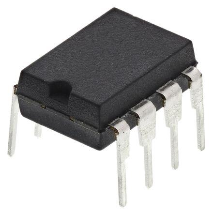
| 供应商器件封装 | 8-PDIP |
| 其它名称 | 296-12533-5 |
| 包装 | 管件 |
| 单位重量 | 440.400 mg |
| 商标 | Texas Instruments |
| 安装类型 | 通孔 |
| 安装风格 | Through Hole |
| 封装 | Tube |
| 封装/外壳 | 8-DIP(0.300",7.62mm) |
| 封装/箱体 | PDIP-8 |
| 工作温度 | -40°C ~ 125°C |
| 工厂包装数量 | 50 |
| 延迟时间 | 25ns |
| 最大功率耗散 | 780 mW |
| 最大工作温度 | + 125 C |
| 最小工作温度 | - 40 C |
| 标准包装 | 50 |
| 激励器数量 | 2 Driver |
| 电压-电源 | 4.5 V ~ 15 V |
| 电流-峰值 | 4A |
| 电源电压-最大 | 15 V |
| 电源电压-最小 | 4 V |
| 电源电流 | 0.75 mA |
| 类型 | Low Side |
| 系列 | UCC27324 |
| 输入类型 | 非反相 |
| 输出数 | 2 |
| 输出电流 | 4 A |
| 输出端数量 | 2 |
| 配置 | 低端 |
| 配置数 | 2 |
| 高压侧电压-最大值(自举) | - |


- 商务部:美国ITC正式对集成电路等产品启动337调查
- 曝三星4nm工艺存在良率问题 高通将骁龙8 Gen1或转产台积电
- 太阳诱电将投资9.5亿元在常州建新厂生产MLCC 预计2023年完工
- 英特尔发布欧洲新工厂建设计划 深化IDM 2.0 战略
- 台积电先进制程称霸业界 有大客户加持明年业绩稳了
- 达到5530亿美元!SIA预计今年全球半导体销售额将创下新高
- 英特尔拟将自动驾驶子公司Mobileye上市 估值或超500亿美元
- 三星加码芯片和SET,合并消费电子和移动部门,撤换高东真等 CEO
- 三星电子宣布重大人事变动 还合并消费电子和移动部门
- 海关总署:前11个月进口集成电路产品价值2.52万亿元 增长14.8%


PDF Datasheet 数据手册内容提取
Product Order Technical Tools & Support & Folder Now Documents Software Community UCC27323,UCC27324,UCC27325 UCC37323,UCC37324,UCC37325 SLUS492J–JUNE2001–REVISEDSEPTEMBER2018 UCCx732x Dual 4-A Peak High-Speed Low-Side Power-MOSFET Drivers 1 Features 3 Description • Bi-CMOSOutputArchitecture The UCC2732x and UCC3732x family of high-speed 1 dual-MOSFET Drivers deliver 4-A source and 4-A • ±4ADriveCurrentattheMillerPlateauRegion sinkpeakcurrenttoeffectivelydriveMOSFETswhere • Constant-CurrentEvenatLowSupplyVoltages it is needed most at the Miller Plateau Region. A • OutputsParalleledforHigherDriveCurrent unique BiPolar and MOSFET hybrid output stage in parallel also allows efficient current sourcing and • AvailableinMSOP-PowerPAD™Package sinking at low supply voltages. Three standard logic • TTL/CMOSInputsIndependentofSupplyVoltage options are offered — dual-inverting, dual- • Industry-StandardPin-Out noninverting, and one-inverting and one-noninverting driver. Input thresholds are based on TTL and CMOS 2 Applications and independent of supply voltage and feature wide input hysteresis offering excellent noise immunity. • Switch-ModePowerSupplies The UCC2732x and UCC3732x family is available in • DC-DCConverters the standard SOIC-8 (D) or PDIP-8 (P) packages as • SolarInverters,MotorControl,UPS well as the thermally enhanced -8pin PowerPAD MSOP package (DGN), drastically lowering thermal resistancetoimprovelongtermreliability. DeviceInformation(1) DEVICE KEYSPECS PACKAGE SOIC(8):4.90mm -40C<=Temp<= ×3.91mm 125C 4.5V<=V <=15V MSOP-PowerPAD DD UCCx732x 20ns/15ns-Rise/Fall (8):3.00mm×3.00 times@1.8nFload mm 35ns/25nsRise/Fall PDIP(8):9.81mm PropDelay ×6.35mm (1) For all available packages, see the orderable addendum at theendofthedatasheet. SimplifiedApplicationDiagram UCCx732x 1 N/C N/C 8 INA 2 INA OUTA 7 3 GND VDD 6 INB 4 INB OUTB 5 0.1μF 1.0μF Copyright © 2016, Texas Instruments Incorporated 1 An IMPORTANT NOTICE at the end of this data sheet addresses availability, warranty, changes, use in safety-critical applications, intellectualpropertymattersandotherimportantdisclaimers.PRODUCTIONDATA.
UCC27323,UCC27324,UCC27325 UCC37323,UCC37324,UCC37325 SLUS492J–JUNE2001–REVISEDSEPTEMBER2018 www.ti.com Table of Contents 1 Features.................................................................. 1 8.4 DeviceFunctionalModes........................................10 2 Applications........................................................... 1 9 ApplicationandImplementation........................ 11 3 Description............................................................. 1 9.1 ApplicationInformation............................................11 4 RevisionHistory..................................................... 2 9.2 TypicalApplication .................................................12 5 DeviceComparisonTable..................................... 3 10 PowerSupplyRecommendations..................... 16 6 PinConfigurationandFunctions......................... 4 11 Layout................................................................... 17 11.1 LayoutGuidelines.................................................17 7 Specifications......................................................... 5 11.2 LayoutExample....................................................17 7.1 AbsoluteMaximumRatings......................................5 11.3 ThermalConsiderations........................................18 7.2 ESDRatings..............................................................5 12 DeviceandDocumentationSupport................. 19 7.3 RecommendedOperatingConditions.......................5 7.4 ThermalInformation..................................................5 12.1 DocumentationSupport........................................19 7.5 ElectricalCharacteristics...........................................6 12.2 RelatedLinks........................................................19 7.6 SwitchingCharacteristics..........................................6 12.3 ReceivingNotificationofDocumentationUpdates19 7.7 TypicalCharacteristics..............................................8 12.4 CommunityResource............................................19 12.5 Trademarks...........................................................19 8 DetailedDescription.............................................. 9 12.6 ElectrostaticDischargeCaution............................19 8.1 Overview...................................................................9 12.7 Glossary................................................................20 8.2 FunctionalBlockDiagram.........................................9 13 Mechanical,Packaging,andOrderable 8.3 FeatureDescription...................................................9 Information........................................................... 20 4 Revision History NOTE:Pagenumbersforpreviousrevisionsmaydifferfrompagenumbersinthecurrentversion. ChangesfromRevisionI(July2016)toRevisionJ Page • ChangedNCdescriptionfrom"Noconnection:mustbegrounded”to“NoInternalConnection".......................................... 4 ChangesfromRevisionH(May2013)toRevisionI Page • AddedESDRatingstable,FeatureDescriptionsection,DeviceFunctionalModes,ApplicationandImplementation section,PowerSupplyRecommendationssection,Layoutsection,DeviceandDocumentationSupportsection,and Mechanical,Packaging,andOrderableInformationsection ................................................................................................. 1 • DeletedPowerDissipationrowsfromAbsoluteMaximumRatings ...................................................................................... 5 ChangesfromRevisionG(March2010)toRevisionH Page • ChangedD diodedirectionandvoltageofzenerdiodefrom5.5to4.5VinFigure7............................................ 13 SCHOTTKY • AddedthreeparagraphsafterfirstparagraphofOperationalWaveformsandCircuitLayoutsectionbeforeFigure9.......16 2 SubmitDocumentationFeedback Copyright©2001–2018,TexasInstrumentsIncorporated ProductFolderLinks:UCC27323 UCC27324 UCC27325UCC37323 UCC37324 UCC37325
UCC27323,UCC27324,UCC27325 UCC37323,UCC37324,UCC37325 www.ti.com SLUS492J–JUNE2001–REVISEDSEPTEMBER2018 5 Device Comparison Table TEMPERATURE PACKAGEDDEVICES(1) OUTPUTCONFIGURATION RANGE MSOP-8PowerPAD TA=TJ SOIC-8(D) (DGN)(2) PDIP-8(P) –40°Cto+125°C UCC27323D UCC27323DGN UCC27323P Dualinverting 0°Cto+70°C UCC37323D UCC37323DGN UCC37323P –40°Cto+125°C UCC27324D UCC27324DGN UCC27324P Dualnoninverting 0°Cto+70°C UCC37324D UCC37324DGN UCC37324P –40°Cto+125°C UCC27325D UCC27325DGN UCC27325P Oneinverting,onenoninverting 0°Cto+70°C UCC37325D UCC37325DGN UCC37325P (1) D(SOIC-8)andDGN(PowerPAD-MSOP)packagesareavailabletapedandreeled.AddRsuffixtodevicetype(forexample UCC27323DR,UCC27324DGNR)toorderquantitiesof2,500devicesperreelforDor1,000devicesperreelforDGNpackage. (2) ThePowerPADisnotdirectlyconnectedtoanyleadsofthepackage.However,thePowerPADiselectricallyandthermallyconnectedto thesubstratewhichisthegroundofthedevice. Copyright©2001–2018,TexasInstrumentsIncorporated SubmitDocumentationFeedback 3 ProductFolderLinks:UCC27323 UCC27324 UCC27325UCC37323 UCC37324 UCC37325
UCC27323,UCC27324,UCC27325 UCC37323,UCC37324,UCC37325 SLUS492J–JUNE2001–REVISEDSEPTEMBER2018 www.ti.com 6 Pin Configuration and Functions D,DGN,orPPackage 8-PinSOIC,MSOPWithPowerPAD,orPDIP TopView PinFunctions PIN I/O DESCRIPTION NAME NO. Commonground:ThisgroundshouldbeconnectedverycloselytothesourceofthepowerMOSFET GND 3 — whichthedriverisdriving. InputA:InputsignaloftheAdriverwhichhaslogiccompatiblethresholdandhysteresis.Ifnotused, INA 2 I thisinputmustbetiedtoeitherVDDorGND;itmustnotbeleftfloating. InputB:InputsignaloftheAdriverwhichhaslogiccompatiblethresholdandhysteresis.Ifnotused, INB 4 I thisinputmustbetiedtoeitherVDDorGND;itmustnotbeleftfloating. N/C 1 — NoInternalConnection N/C 8 — NoInternalConnection DriveroutputA:Theoutputstageiscapableofproviding4-Adrivecurrenttothegateofapower OUTA 7 O MOSFET. DriveroutputB:Theoutputstageiscapableofproviding4-Adrivecurrenttothegateofapower OUTB 5 O MOSFET. VDD 6 I Supply:Supplyvoltageandthepowerinputconnectionforthisdevice. 4 SubmitDocumentationFeedback Copyright©2001–2018,TexasInstrumentsIncorporated ProductFolderLinks:UCC27323 UCC27324 UCC27325UCC37323 UCC37324 UCC37325
UCC27323,UCC27324,UCC27325 UCC37323,UCC37324,UCC37325 www.ti.com SLUS492J–JUNE2001–REVISEDSEPTEMBER2018 7 Specifications 7.1 Absolute Maximum Ratings overoperatingfree-airtemperaturerange(unlessotherwisenoted)(1)(2) MIN MAX UNIT Analoginputvoltage(INA,INB) –0.3toV +0.3V nottoexceed16 V DD OutputbodydiodeDCcurrent(OUTA,OUTB) 0.2 I DC 0.2 A OUT_DC Outputcurrent(OUTA,OUTB) IOUT_PULSED Pulsed(0.5µs) 4.5 Outputvoltage(OUTA,OUTB) 16 V V Supplyvoltage –0.3 16 V DD T Junctionoperatingtemperature –55 150 J °C T Storagetemperature –65 150 stg (1) StressesbeyondthoselistedunderAbsoluteMaximumRatingsmaycausepermanentdamagetothedevice.Thesearestressratings only,whichdonotimplyfunctionaloperationofthedeviceattheseoranyotherconditionsbeyondthoseindicatedunderRecommended OperatingConditions.Exposuretoabsolute-maximum-ratedconditionsforextendedperiodsmayaffectdevicereliability. (2) AllvoltagesarewithrespecttoGND.Currentsarepositiveinto,negativeoutofthespecifiedterminal. 7.2 ESD Ratings VALUE UNIT Human-bodymodel(HBM),perANSI/ESDA/JEDECJS-001(1) 4000 V(ESD) Electrostaticdischarge Charged-devicemodel(CDM),perJEDECspecificationJESD22- V C101(2) 1000 (1) JEDECdocumentJEP155statesthat500-VHBMallowssafemanufacturingwithastandardESDcontrolprocess. (2) JEDECdocumentJEP157statesthat250-VCDMallowssafemanufacturingwithastandardESDcontrolprocess. 7.3 Recommended Operating Conditions overoperatingfree-airtemperaturerange(unlessotherwisenoted) MIN NOM MAX UNIT Supplyvoltage 4.5 15 V Inputvoltage 0 15 V UCC2732x –40 125 °C Operatingjunctiontemperature UCC3732x 0 70 °C 7.4 Thermal Information UCCx732x DGN THERMALMETRIC(1) D (MSOPWith P UNIT (SOIC) (PDIP) PowerPAD) 8PINS 8PINS 8PINS R Junction-to-ambientthermalresistance 107.3 56.6 55.5 °C/W θJA R Junction-to-case(top)thermalresistance 52.2 52.8 45.3 °C/W θJC(top) R Junction-to-boardthermalresistance 47.3 32.6 32.6 °C/W θJB ψ Junction-to-topcharacterizationparameter 10.2 1.8 23 °C/W JT ψ Junction-to-boardcharacterizationparameter 46.8 32.3 32.5 °C/W JB R Junction-to-case(bottom)thermalresistance N/A 5.9 N/A °C/W θJC(bot) (1) Formoreinformationabouttraditionalandnewthermalmetrics,seetheSemiconductorandICPackageThermalMetricsapplication report. Copyright©2001–2018,TexasInstrumentsIncorporated SubmitDocumentationFeedback 5 ProductFolderLinks:UCC27323 UCC27324 UCC27325UCC37323 UCC37324 UCC37325
UCC27323,UCC27324,UCC27325 UCC37323,UCC37324,UCC37325 SLUS492J–JUNE2001–REVISEDSEPTEMBER2018 www.ti.com 7.5 Electrical Characteristics V =4.5to15V,T =T (unlessotherwisenoted) DD A J PARAMETER TESTCONDITIONS MIN TYP MAX UNIT INPUT(INA,INB) V Logic1inputthreshold 2 IN_H V V Logic0inputthreshold 1 IN_L Inputcurrent 0V←V ←V –10 10 µA IN DD OUTPUT(OUTA,OUTB) Outputcurrent V =14V(1) 4 A DD V High-leveloutputvoltage V =V –V ,I =–10mA 300 450 OH OH DD OUT OUT mV V Low-leveloutputlevel I =10mA 22 45 OL OUT T =25°C,I =–10mA,V =14V(2) 25 30 35 A OUT DD Outputresistancehigh T =fullrange,I =–10mA,V =14V(2) 18 42 A OUT DD Ω T =25°C,I =10mA,V =14V(2) 1.9 2.2 2.5 A OUT DD Outputresistancelow T =fullrange,I =10mA,V =14V(2) 1.2 4 A OUT DD Latch-upprotection 500 mA OVERALL INA=0V,INB=0V 300 450 INA=0V,INB=HIGH 300 450 UCCx7323 INA=HIGH,INB=0V 300 450 INA=HIGH,INB=HIGH 300 450 INA=0V,INB=0V 2 50 StaticOperating INA=0V,INB=HIGH 300 450 I UCCx7324 µA DD Current INA=HIGH,INB=0V 300 450 INA=HIGH,INB=HIGH 600 750 INA=0V,INB=0V 150 300 INA=0V,INB=HIGH 450 600 UCCx7325 INA=HIGH,INB=0V 150 300 INA=HIGH,INB=HIGH 450 600 (1) ThepullupandpulldowncircuitsofthedriverarebipolarandMOSFETtransistorsinparallel.Thepulsedoutputcurrentratingisthe combinedcurrentfromthebipolarandMOSFETtransistors. (2) ThepullupandpulldowncircuitsofthedriverarebipolarandMOSFETtransistorsinparallel.TheoutputresistanceistheR ofthe DS(ON) MOSFETtransistorwhenthevoltageonthedriveroutputislessthanthesaturationvoltageofthebipolartransistor. 7.6 Switching Characteristics overoperatingfree-airtemperaturerange(unlessotherwisenoted) PARAMETER TESTCONDITIONS MIN TYP MAX UNIT T Risetime(OUTA,OUTB) C =1.8nF,seeFigure1 20 40 R LOAD T Falltime(OUTA,OUTB) C =1.8nF,seeFigure1 15 40 F LOAD ns T Delay,INrising(INtoOUT) C =1.8nF,seeFigure1 25 40 D1 LOAD T Delay,INfalling(INtoOUT) C =1.8nF,seeFigure1 35 35 D2 LOAD 6 SubmitDocumentationFeedback Copyright©2001–2018,TexasInstrumentsIncorporated ProductFolderLinks:UCC27323 UCC27324 UCC27325UCC37323 UCC37324 UCC37325
UCC27323,UCC27324,UCC27325 UCC37323,UCC37324,UCC37325 www.ti.com SLUS492J–JUNE2001–REVISEDSEPTEMBER2018 (a) (b) +5V 90% 90% INPUT INPUT 10% 10% 0V tD1 tF tD2 tR tF tR 16V 90% 90% 90% tD1 OUTPUT OUTPUT tD2 10% 10% 0V Figure1. SwitchingWaveformsfor(a)InvertingDriverand(b)NoninvertingDriver Copyright©2001–2018,TexasInstrumentsIncorporated SubmitDocumentationFeedback 7 ProductFolderLinks:UCC27323 UCC27324 UCC27325UCC37323 UCC37324 UCC37325
UCC27323,UCC27324,UCC27325 UCC37323,UCC37324,UCC37325 SLUS492J–JUNE2001–REVISEDSEPTEMBER2018 www.ti.com 7.7 Typical Characteristics 30 38 28 36 10 nF 26 10 nF 34 ime - nsT 2224 4.7 nF me - ns 3320 4.7 nF y iT ela 20 ay 28 tD1 - D 18 D2 - Del 26 2.2 nF 2.2 nF t 16 24 470 pF 1 nF 14 470 pF 22 1 nF 12 20 4 6 8 10 12 14 16 4 6 8 10 12 14 16 VDD- Supply Voltage - V VDD- Supply Voltage - V Figure2.DelayTime(tD1)vsSupplyVoltage Figure3.DelayTime(tD2)vsSupplyVoltage 2.0 1.9 VDD= 15 V V e - 1.8 g a oltd V1.7 ol h es1.6 hr T put 1.5 VDD= 10 V n - ION1.4 VDD= 4.5 V V 1.3 1.2 -50 -25 0 25 50 75 100 125 TJ- Temperature -°C Figure4.InputThresholdvsTemperature 8 SubmitDocumentationFeedback Copyright©2001–2018,TexasInstrumentsIncorporated ProductFolderLinks:UCC27323 UCC27324 UCC27325UCC37323 UCC37324 UCC37325
UCC27323,UCC27324,UCC27325 UCC37323,UCC37324,UCC37325 www.ti.com SLUS492J–JUNE2001–REVISEDSEPTEMBER2018 8 Detailed Description 8.1 Overview The UCC2732x and UCC3732x family of high-speed dual MOSFET drivers can deliver large peak currents into capacitive loads. Three standard logic options are offered – dual-inverting, dual-noninverting and one-inverting and one-noninverting driver. Using a design that inherently minimizes shoot-through current, these drivers deliver 4A of current where it is needed most at the Miller plateau region during the MOSFET switching transition. A unique Bipolar and MOSFET hybrid output stage in parallel also allows efficient current sourcing and sinking at lowsupplyvoltages. 8.2 Functional Block Diagram INVERTING N/C 1 8 N/C 7 OUTA INA 2 NON-INVERTING GND 3 INVERTING 6 VDD 5 OUTB INB 4 NON-INVERTING Copyright © 2016, Texas Instruments Incorporated 8.3 Feature Description 8.3.1 InputStage The input thresholds have a 3.3-V logic sensitivity over the full range of V voltage; yet it is equally compatible DD with0VtoV signals. DD The inputs of UCC2732x and UCC3732x family of drivers are designed to withstand 500-mA reverse current without either damage to the IC for logic upset. The input stage of each driver must be driven by a signal with a short rise or fall time. This condition is satisfied in typical power-supply applications, where the input signals are provided by a PWM controller or logic gates with fast transition times (<200 ns). The input stages to the drivers function as a digital gate, and are not intended for applications where a slow-changing input voltage is used to generate a switching output when the logic threshold of the input section is reached. While this may not be harmfultothedriver,theoutputofthedrivermayswitchrepeatedlyatahighfrequency. Users should not attempt to shape the input signals to the driver in an attempt to slow down (or delay) the signal at the output. If limited rise or fall times to the power device is desired, an external resistance can be added between the output of the driver and the load device, which is generally a power MOSFET gate. The external resistor may also help remove power dissipation from the device package, as discussed in (see Thermal Considerations). Importantly, input signal of the two channels, INA and INB, which has logic compatible threshold and hysteresis. Ifnotused,INAandINBmustbetiedtoeitherVDDorGND;itmustnotbeleftfloating. 8.3.2 OutputStage Inverting outputs of the UCCx7323 and OUTA of the UCCx7325 are intended to drive external P-channel MOSFETs. Noninverting outputs of the UCCx7324 and OUTB of the UCCx7325 are intended to drive external N- ChannelMOSFETs. Copyright©2001–2018,TexasInstrumentsIncorporated SubmitDocumentationFeedback 9 ProductFolderLinks:UCC27323 UCC27324 UCC27325UCC37323 UCC37324 UCC37325
UCC27323,UCC27324,UCC27325 UCC37323,UCC37324,UCC37325 SLUS492J–JUNE2001–REVISEDSEPTEMBER2018 www.ti.com Feature Description (continued) Each output stage is capable of supplying ±4-A peak current pulses and swings to both VDD and GND. The pullupandpulldowncircuitsofthedriverareconstructedofbipolarandMOSFETtransistorsinparallel.Thepeak output current rating is the combined current from the bipolar and MOSFET transistors. The output resistance is the R of the MOSFET transistor when the voltage on the driver output is less than the saturation voltage of DS(on) thebipolartransistor.Eachoutputstagealsoprovidesaverylowimpedancetoovershootandundershootdueto thebodydiodeoftheexternalMOSFET. This means that in many cases, external-Schottky-clamp diodes are not required. The UCCx732x family delivers 4AofgatedrivewhereitismostneededduringtheMOSFETswitchingtransition –attheMillerplateauregion – providing improved efficiency gains. A unique Bipolar and MOSFET hybrid output stage in parallel also allows efficientcurrentsourcingatlowsupplyvoltages. 8.4 Device Functional Modes With VDD power supply in the range of 4.5 V to 15 V, the output stage is dependent on the states of the HI and LIpins.Table1showstheUCCx732xtruthtable. Table1.InputandOutputTable INPUTS(VIN_L,VIN_H) UCC37323x UCC37324x UCC37325x INA INB OUTA OUTB OUTA OUTB OUTA OUTB L L H H L L H L L H H L L H H H H L L H H L L L H H L L H H L H Importantly,ifINAandINBarenotused,theymustbetiedtoeitherVDDorGND;itmustnotbeleftfloating. 10 SubmitDocumentationFeedback Copyright©2001–2018,TexasInstrumentsIncorporated ProductFolderLinks:UCC27323 UCC27324 UCC27325UCC37323 UCC37324 UCC37325
UCC27323,UCC27324,UCC27325 UCC37323,UCC37324,UCC37325 www.ti.com SLUS492J–JUNE2001–REVISEDSEPTEMBER2018 9 Application and Implementation NOTE Information in the following applications sections is not part of the TI component specification, and TI does not warrant its accuracy or completeness. TI’s customers are responsible for determining suitability of components for their purposes. Customers should validateandtesttheirdesignimplementationtoconfirmsystemfunctionality. 9.1 Application Information High-frequency power supplies often require high-speed, high-current drivers such as the UCCx732x family. A leading application is the needed to provide a high-power buffer stage between the PWM output of the control IC and the gates of the primary power MOSFET or IGBT switching devices. In other cases, the driver IC is used to drive the power-device gates through a drive transformer. Synchronous rectification supplies are also needed to simultaneouslydrivemultipledeviceswhichpresentsanextremelylargeloadtothecontrolcircuitry. Driver ICs are used when having the primary PWM regulator IC directly drive the switching devices for one or more reasons is not feasible. The PWMIC does not have the brute drive capability required for the intended switching MOSFET, limiting the switching performance in the application. In other cases there may be a desire to minimize the effect of high-frequency switching noise by placing the high current driver physically close to the load. Also, newer ICs that target the highest operating frequencies do not incorporate onboard gate drivers at all. Their PWM outputs are only intended to drive the high impedance input to a driver such as the UCCx732x. Finally, the control IC is under thermal stress due to power dissipation, and an external driver helps by moving theheatfromthecontrollertoanexternalpackage. Copyright©2001–2018,TexasInstrumentsIncorporated SubmitDocumentationFeedback 11 ProductFolderLinks:UCC27323 UCC27324 UCC27325UCC37323 UCC37324 UCC37325
UCC27323,UCC27324,UCC27325 UCC37323,UCC37324,UCC37325 SLUS492J–JUNE2001–REVISEDSEPTEMBER2018 www.ti.com 9.2 Typical Application UCCx732x 1 N/C N/C 8 INA 2 INA OUTA 7 3 GND VDD 6 INB 4 INB OUTB 5 0.1μF 1.0μF Copyright © 2016, Texas Instruments Incorporated Figure5. UCCx732xDrivingTwoIndependentMOSFETs 9.2.1 DesignRequirements To select proper device from UCCx732x family, TI recommends first checking the appropriate logic for the outputs. UCCx7323 has dual inverting outputs; UCCx7324 has dual noninverting outputs; UCCx7325 have invertingchannelAandnoninvertingchannelB.Moreover,somedesignconsiderationsmustbeevaluatedfirstin order to make the most appropriate selection. Among these considerations are VDD, drive current, and power dissipation. 9.2.2 DetailedDesignProcedure 9.2.2.1 Source/SinkCapabilitiesDuringMillerPlateau Large power MOSFETs present a large load to the control circuitry. Proper drive is required for efficient, reliable operation. The UCCx732x drivers have been optimized to provide maximum drive to a power MOSFET during the Miller plateau region of the switching transition. This interval occurs while the drain voltage is swinging between the voltage levels dictated by the power topology, requiring the charging/discharging of the drain-gate capacitancewithcurrentsuppliedorremovedbythedriverdevice[1]. Two circuits are used to test the current capabilities of the UCCx732x driver. In each case external circuitry is added to clamp the output near 5 V while the IC is sinking or sourcing current. An input pulse of 250 ns is applied at a frequency of 1 kHz in the proper polarity for the respective test. In each test there is a transient period where the current peaked up and then settled down to a steady-state value. The noted current measurementsaremadeatatimeof200nsaftertheinputpulseisapplied,aftertheinitialtransient.[1] The first circuit in Figure 6 is used to verify the current sink capability when the output of the driver is clamped around 5 V, a typical value of gate-source voltage during the Miller plateau region. The UCCx7323 is found to sink4.5AatVDD=15Vand4.28AatVDD=12V. 12 SubmitDocumentationFeedback Copyright©2001–2018,TexasInstrumentsIncorporated ProductFolderLinks:UCC27323 UCC27324 UCC27325UCC37323 UCC37324 UCC37325
UCC27323,UCC27324,UCC27325 UCC37323,UCC37324,UCC37325 www.ti.com SLUS492J–JUNE2001–REVISEDSEPTEMBER2018 Typical Application (continued) UCCx7323 VDD 1 N/C N/C 8 D 10Ω INA OUTA SCHOTTKY 2 7 V 3 GND VDD 6 ADJ 1µF CER 100µF 5.5V ALEL Signal INB OUTB 4 5 Generator V SNS producing 250ns wide R pulse 0.S1NSΩ 1µF CER 100µF ALEL Copyright © 2016,Texas Instruments Incorporated Figure6. CurrentSinkCapabilityTest The circuit shown in Figure 7 is used to test the current source capability with the output clamped to around 5 V withastringofZenerdiodes.TheUCCx7323isfoundtosource4.8AatVDD=15Vand3.7AatVDD=12V. UCCx7323 VDD 1 N/C N/C 8 INA OUTA DSCHOTTKY 10Ω 2 7 3 GND VDD 6 4.5V 1 µF CER 100 µF ALEL INB OUTB Signal 4 5 Generator V SNS producing 250 ns wide pulse R SNS 0.1Ω 1µF CER 100 µF ALEL Copywright © 2016,Texas Instruments Incorporated Figure7. CurrentSourceCapabilityTest Copyright©2001–2018,TexasInstrumentsIncorporated SubmitDocumentationFeedback 13 ProductFolderLinks:UCC27323 UCC27324 UCC27325UCC37323 UCC37324 UCC37325
UCC27323,UCC27324,UCC27325 UCC37323,UCC37324,UCC37325 SLUS492J–JUNE2001–REVISEDSEPTEMBER2018 www.ti.com Typical Application (continued) 9.2.2.2 ParallelOutputs The A and B drivers may be combined into a single driver by connecting the INA/INB inputs together as close to the IC as possible, and the OUTA/OUTB outputs ties together if the external gate drive resistor is not used. In somecaseswheretheexternalgatedriveresistorisused,Tirecommendsthattheresistorcanbeequallysplitin OUTA and OUTB respectively to reduce the parasitic inductance induce unbalance between two channels, as showinFigure8. UCCx7323/4 1 N/C N/C 8 R G IN 2 INA OUTA 7 3 GND VDD 6 R G 4 INB OUTB 5 0.1(cid:29)F 1.0(cid:29)F Figure8. ParallelOperationofUCCx7323andUCCx7324 Important consideration about paralleling two channels for UCCx7323/4 include: 1) INA and INB should be shorted in PCB layout as close to the device as possible, as well as for OUTA and OUTB, in which condition PCB layout parasitic mismatching between two channels could be minimized. 2) INA/B input slope signal should be fast enough to avoid mismatched V /V , t /t between channel-A and channel-B. TI recommends IN_H IN_L d1 d2 havinginputsignalslopefasterthan20V/us. 9.2.2.3 VDD Although quiescent VDD current is very low, total supply current will be higher, depending on OUTA and OUTB currentandtheprogrammedoscillatorfrequency.TotalVDDcurrentisthesumofquiescentVDDcurrentandthe average OUT current. Knowing the operating frequency and the MOSFET gate charge (Q ), average OUT g currentcanbecalculatedusingEquation1. I =Q ×f OUT g wherefisfrequency (1) For the best high-speed circuit performance, two VDD bypass capacitors are recommended to prevent noise problems. The use of surface mount components is highly recommended. A 0.1-µF ceramic capacitor should be located closest to the VDD to ground connection. In addition, a larger capacitor (such as 1 µF and above) with relativelylowESRshouldbeconnectedinparallel,tohelpdeliverthehighcurrentpeakstotheload.Theparallel combination of capacitors should present a low impedance characteristic for the expected current levels in the driverapplication. 9.2.2.4 DriverCurrentandPowerRequirements The UCCx732x family of drivers is capable of delivering 4 A of current to a MOSFET gate for a period of tens of nanoseconds. High peak current is required to turn the device ON quickly. Then, to turn the device OFF, the driver is required to sink a similar amount of current to ground. This repeats at the operating frequency of the power device. A MOSFET is used in this discussion because it is the most common type of switching device usedinhigh-frequencypowerconversionequipment. 14 SubmitDocumentationFeedback Copyright©2001–2018,TexasInstrumentsIncorporated ProductFolderLinks:UCC27323 UCC27324 UCC27325UCC37323 UCC37324 UCC37325
UCC27323,UCC27324,UCC27325 UCC37323,UCC37324,UCC37325 www.ti.com SLUS492J–JUNE2001–REVISEDSEPTEMBER2018 Typical Application (continued) Reference[1]andreference[2]discussthecurrentrequiredtodriveapowerMOSFETandothercapacitive-input switchingdevices.Reference[2]includesinformationonthepreviousgenerationofbipolarICgatedrivers. WhenadriverICistestedwithadiscrete,capacitiveload,itisafairlysimplemattertocalculatethepowerthatis required from the bias supply. The energy that must be transferred from the bias supply to charge the capacitor isgivenbyEquation2. E=½CV2 where • Cistheloadcapacitor • Visthebiasvoltagefeedingthedriver (2) There is an equal amount of energy transferred to ground when the capacitor is discharged. This leads to a powerlossgivenbyEquation3. P=CV2×f wherefistheswitchingfrequency (3) This power is dissipated in the resistive elements of the circuit. Thus, with no external resistor between the driver and gate, this power is dissipated inside the driver. Half of the total power is dissipated when the capacitor is charged, and the other half is dissipated when the capacitor is discharged. An actual example using the conditionsofthepreviousgatedrivewaveformshouldhelpclarifythis. WithV =12V,C =10nF,andf=300kHz,thepowerlosscanbecalculatedasEquation4. DD LOAD P=10nF×(12V)2×(300kHz)=0.432W (4) Witha12-Vsupply,thisequatestoacurrentof(seeEquation5): I=P/V=0.432W/12V=36mA (5) The actual current measured from the supply was 0.037 A, and is very close to the predicted value. But, the I DD current that is due to the IC internal consumption should be considered. With no load the IC current draw is 0.0027 A. Under this condition the output rise and fall times are faster than with a load. This could lead to an almost insignificant, yet measurable current due to cross-conduction in the output stages of the driver. However, these small current differences are buried in the high frequency switching spikes, and are beyond the measurement capabilities of a basic lab setup. The measured current with 10-nF load is reasonably close to that expected. The switching load presented by a power MOSFET can be converted to an equivalent capacitance by examining the gate charge required to switch the device. This gate charge includes the effects of the input capacitance plus the added charge needed to swing the drain of the device between the ON and OFF states. Most manufacturers provide specifications that provide the typical and maximum gate charge, in nC, to switch the device under specified conditions. Using the gate charge Q , one can determine the power that must be dissipated when g chargingacapacitor.ThisisdonebyusingtheequivalenceQ =C ×VtoprovideEquation6 forpower: g eff P=C×V2×f=V×Q ×f (6) g Equation 6 allows a power designer to calculate the bias power required to drive a specific MOSFET gate at a specificbiasvoltageandaspecificswitchingfrequency. 9.2.3 ApplicationCurves Figure 9 shows the circuit performance achievable with a single driver (half of the 8-pin IC) driving a 10-nF load. The input pulse width (not shown) is set to 300 ns to show both transitions in the output waveform. Note the linear rise and fall edges of the switching waveforms which is due to the constant output current characteristic of thedriverasopposedtotheresistiveoutputimpedanceoftraditionalMOSFET-basedgatedrivers. Sink and source currents of the driver are dependent upon the VDD value and the output capacitive load. The larger the VDD value, the higher the current capability; also, the larger the capacitive load, the higher the current sinkandsourcecapability. Trace resistance and inductance, including wires and cables for testing, slows down the rise and fall times of the outputs;thusreducingthecurrentcapabilitiesofthedriver. Copyright©2001–2018,TexasInstrumentsIncorporated SubmitDocumentationFeedback 15 ProductFolderLinks:UCC27323 UCC27324 UCC27325UCC37323 UCC37324 UCC37325
UCC27323,UCC27324,UCC27325 UCC37323,UCC37324,UCC37325 SLUS492J–JUNE2001–REVISEDSEPTEMBER2018 www.ti.com Typical Application (continued) To achieve higher current results, reduce resistance and inductance on the board as much as possible and increasethecapacitiveloadvalueinordertoswampouttheeffectofinductancevalues. C =10nF,C =10nF,VDD=12V L L Figure9. RisingandFallingTimeofUCCx732x 10 Power Supply Recommendations TherecommendedbiassupplyvoltagerangeforUCCx732xisfrom4.5Vto15V.Theupperendofthisrangeis driven by the 16 V absolute maximum voltage rating of the VDD. TI recommends keeping proper margin to allow fortransientvoltagespikes. A local bypass capacitor must be placed between the VDD and GND pins. And this capacitor must be placed as close to the device as possible. A low ESR, ceramic surface mount capacitor is recommended. TI recommends using 2 capacitors across VDD and GND: a 100-nF ceramic surface-mount capacitor for high frequency filtering placedveryclosetoVDDandGNDpin,andanothersurface-mountcapacitor,220nFto 10µF,forICbiasrequirements. 16 SubmitDocumentationFeedback Copyright©2001–2018,TexasInstrumentsIncorporated ProductFolderLinks:UCC27323 UCC27324 UCC27325UCC37323 UCC37324 UCC37325
UCC27323,UCC27324,UCC27325 UCC37323,UCC37324,UCC37325 www.ti.com SLUS492J–JUNE2001–REVISEDSEPTEMBER2018 11 Layout 11.1 Layout Guidelines Optimum performance of high and low-side gate drivers cannot be achieved without taking due considerations duringcircuitboardlayout.Thefollowingpointsareemphasized: 1) Low ESR/ESL capacitors must be connected close to the IC between VDD and GND pins to support high peakcurrentsdrawnfromVDDduringtheturn-onoftheexternalMOSFETs. 2)Groundingconsiderations: The first priority in designing grounding connections is to confine the high peak currents that charge and discharge the MOSFET gates to a minimal physical area. This will decrease the loop inductance and minimize noise issues on the gate terminals of the MOSFETs. The gate driver must be placed as close as possibletotheMOSFETs. Star-point grounding is a good way to minimize noise coupling from one current loop to another. The GND of the driver is connected to the other circuit nodes such as source of power MOSFET and ground of PWM controller at one, single point. The connected paths must be as short as possible to reduce inductance and beaswideaspossibletoreduceresistance. Use a ground plane to provide noise shielding. Fast rise and fall times at OUT may corrupt the input signals during transition. The ground plane must not be a conduction path for any current loop. Instead the ground plane must be connected to the star-point with one single trace to establish the ground potential. In addition tonoiseshielding,thegroundplanecanhelpinpowerdissipationaswell. 3)Innoisyenvironments,tyinginputsofanunusedchanneloftheUCC2742xdevicetoVDDorGNDusingshort traces in order to ensure that the output is enabled and to prevent noise from causing malfunction in the output maybenecessary. 4)Separatepowertracesandsignaltraces,suchasoutputandinputsignals. 11.2 Layout Example UCCx732x Ground plane (Bottom Layer) Ext. Gate Resistance (Ch-A) INA OUTA To Ch-A GND VDD Load INB OUTB To Ch-B Load Ext. Gate Resistance Bypassing Cap, 0.1(cid:29)F (Ch-B) Bypassing Cap, 1.0(cid:29)F Figure10. RecommendedPCBLayoutforUCCx732x Copyright©2001–2018,TexasInstrumentsIncorporated SubmitDocumentationFeedback 17 ProductFolderLinks:UCC27323 UCC27324 UCC27325UCC37323 UCC37324 UCC37325
UCC27323,UCC27324,UCC27325 UCC37323,UCC37324,UCC37325 SLUS492J–JUNE2001–REVISEDSEPTEMBER2018 www.ti.com 11.3 Thermal Considerations The useful range of a driver is greatly affected by the drive power requirements of the load and the thermal characteristicsoftheICpackage.Inorderforapowerdrivertobeusefuloveraparticulartemperaturerange,the package must allow for the efficient removal of the heat produced while keeping the junction temperature within rated limits. The UCCx732x family of drivers is available in three different packages to cover a range of applicationrequirements. The MSOP PowerPAD-8 (DGN) package significantly relieves this concern by offering an effective means of removing the heat from the semiconductor junction. As illustrated in reference [3], the PowerPAD packages offer a lead-frame die pad that is exposed at the base of the package. This pad is soldered to the copper on the PC board directly underneath the IC package, reducing the θ down to 4.7°C/W. Data is presented in reference [3] JC to show that the power dissipation can be quadrupled in the PowerPAD configuration when compared to the standard packages. The PC board must be designed with thermal lands and thermal vias to complete the heat removal subsystem, as summarized in reference [4]. This design allows a significant improvement in heat sinking overthatwhichisavailableintheDorPpackages,andisshowntomorethandoublethepowercapabilityofthe DandPpackages. NOTE The PowerPAD is not directly connected to any leads of the package. However, the PowerPad is electrically and thermally connected to the substrate which is the ground of thedevice. 18 SubmitDocumentationFeedback Copyright©2001–2018,TexasInstrumentsIncorporated ProductFolderLinks:UCC27323 UCC27324 UCC27325UCC37323 UCC37324 UCC37325
UCC27323,UCC27324,UCC27325 UCC37323,UCC37324,UCC37325 www.ti.com SLUS492J–JUNE2001–REVISEDSEPTEMBER2018 12 Device and Documentation Support 12.1 Documentation Support 12.1.1 RelatedDocumentation Seethefollowingforrelateddocumentation: 1. Power Supply Seminar SEM-1400 Topic 2, Design And Application Guide For High Speed MOSFET Gate DriveCircuits(SLUP133) 2. PracticalConsiderationsinHighPerformanceMOSFET,IGBTandMCTGateDriveCircuits (SLUA105) 3. PowerPadThermallyEnhancedPackage(SLMA002) 4. PowerPADMadeEasy(SLMA004) 12.2 Related Links The table below lists quick access links. Categories include technical documents, support and community resources,toolsandsoftware,andquickaccesstosampleorbuy. Table2.RelatedLinks TECHNICAL TOOLS& SUPPORT& PARTS PRODUCTFOLDER SAMPLE&BUY DOCUMENTS SOFTWARE COMMUNITY UCC27323 Clickhere Clickhere Clickhere Clickhere Clickhere UCC27324 Clickhere Clickhere Clickhere Clickhere Clickhere UCC27325 Clickhere Clickhere Clickhere Clickhere Clickhere UCC37323 Clickhere Clickhere Clickhere Clickhere Clickhere UCC37324 Clickhere Clickhere Clickhere Clickhere Clickhere UCC37325 Clickhere Clickhere Clickhere Clickhere Clickhere 12.3 Receiving Notification of Documentation Updates To receive notification of documentation updates, navigate to the device product folder on ti.com. In the upper right corner, click on Alert me to register and receive a weekly digest of any product information that has changed.Forchangedetails,reviewtherevisionhistoryincludedinanyreviseddocument. 12.4 Community Resource The following links connect to TI community resources. Linked contents are provided "AS IS" by the respective contributors. They do not constitute TI specifications and do not necessarily reflect TI's views; see TI's Terms of Use. TIE2E™OnlineCommunity TI'sEngineer-to-Engineer(E2E)Community.Createdtofostercollaboration amongengineers.Ate2e.ti.com,youcanaskquestions,shareknowledge,exploreideasandhelp solveproblemswithfellowengineers. DesignSupport TI'sDesignSupport QuicklyfindhelpfulE2Eforumsalongwithdesignsupporttoolsand contactinformationfortechnicalsupport. 12.5 Trademarks PowerPAD,E2EaretrademarksofTexasInstruments. Allothertrademarksarethepropertyoftheirrespectiveowners. 12.6 Electrostatic Discharge Caution Thesedeviceshavelimitedbuilt-inESDprotection.Theleadsshouldbeshortedtogetherorthedeviceplacedinconductivefoam duringstorageorhandlingtopreventelectrostaticdamagetotheMOSgates. Copyright©2001–2018,TexasInstrumentsIncorporated SubmitDocumentationFeedback 19 ProductFolderLinks:UCC27323 UCC27324 UCC27325UCC37323 UCC37324 UCC37325
UCC27323,UCC27324,UCC27325 UCC37323,UCC37324,UCC37325 SLUS492J–JUNE2001–REVISEDSEPTEMBER2018 www.ti.com 12.7 Glossary SLYZ022—TIGlossary. Thisglossarylistsandexplainsterms,acronyms,anddefinitions. 13 Mechanical, Packaging, and Orderable Information The following pages include mechanical, packaging, and orderable information. This information is the most current data available for the designated devices. This data is subject to change without notice and revision of thisdocument.Forbrowser-basedversionsofthisdatasheet,refertotheleft-handnavigation. 20 SubmitDocumentationFeedback Copyright©2001–2018,TexasInstrumentsIncorporated ProductFolderLinks:UCC27323 UCC27324 UCC27325UCC37323 UCC37324 UCC37325
PACKAGE OPTION ADDENDUM www.ti.com 6-Feb-2020 PACKAGING INFORMATION Orderable Device Status Package Type Package Pins Package Eco Plan Lead/Ball Finish MSL Peak Temp Op Temp (°C) Device Marking Samples (1) Drawing Qty (2) (6) (3) (4/5) UCC27323D ACTIVE SOIC D 8 75 Green (RoHS NIPDAU Level-1-260C-UNLIM -40 to 125 27323 & no Sb/Br) UCC27323DG4 ACTIVE SOIC D 8 75 Green (RoHS NIPDAU Level-1-260C-UNLIM -40 to 125 27323 & no Sb/Br) UCC27323DGN ACTIVE HVSSOP DGN 8 80 Green (RoHS NIPDAUAG Level-1-260C-UNLIM -40 to 125 27323 & no Sb/Br) UCC27323DGNR ACTIVE HVSSOP DGN 8 2500 Green (RoHS NIPDAUAG Level-1-260C-UNLIM -40 to 125 27323 & no Sb/Br) UCC27323DR ACTIVE SOIC D 8 2500 Green (RoHS NIPDAU Level-1-260C-UNLIM -40 to 125 27323 & no Sb/Br) UCC27323DRG4 ACTIVE SOIC D 8 2500 Green (RoHS NIPDAU Level-1-260C-UNLIM -40 to 125 27323 & no Sb/Br) UCC27323P ACTIVE PDIP P 8 50 Pb-Free NIPDAU N / A for Pkg Type -40 to 125 UCC27323P (RoHS) UCC27324D ACTIVE SOIC D 8 75 Green (RoHS NIPDAU Level-1-260C-UNLIM -40 to 125 27324 & no Sb/Br) UCC27324DG4 ACTIVE SOIC D 8 75 Green (RoHS NIPDAU Level-1-260C-UNLIM -40 to 125 27324 & no Sb/Br) UCC27324DGN ACTIVE HVSSOP DGN 8 80 Green (RoHS NIPDAU | NIPDAUAG Level-1-260C-UNLIM -40 to 125 27324 & no Sb/Br) UCC27324DGNG4 ACTIVE HVSSOP DGN 8 80 Green (RoHS NIPDAUAG Level-1-260C-UNLIM -40 to 125 27324 & no Sb/Br) UCC27324DGNR ACTIVE HVSSOP DGN 8 2500 Green (RoHS NIPDAU | NIPDAUAG Level-1-260C-UNLIM -40 to 125 27324 & no Sb/Br) UCC27324DGNRG4 ACTIVE HVSSOP DGN 8 2500 Green (RoHS NIPDAUAG Level-1-260C-UNLIM -40 to 125 27324 & no Sb/Br) UCC27324DR ACTIVE SOIC D 8 2500 Green (RoHS NIPDAU Level-1-260C-UNLIM -40 to 125 27324 & no Sb/Br) UCC27324DRG4 ACTIVE SOIC D 8 2500 Green (RoHS NIPDAU Level-1-260C-UNLIM -40 to 125 27324 & no Sb/Br) UCC27324P ACTIVE PDIP P 8 50 Pb-Free NIPDAU N / A for Pkg Type -40 to 125 UCC27324P (RoHS) UCC27324PE4 ACTIVE PDIP P 8 50 Pb-Free NIPDAU N / A for Pkg Type -40 to 125 UCC27324P (RoHS) Addendum-Page 1
PACKAGE OPTION ADDENDUM www.ti.com 6-Feb-2020 Orderable Device Status Package Type Package Pins Package Eco Plan Lead/Ball Finish MSL Peak Temp Op Temp (°C) Device Marking Samples (1) Drawing Qty (2) (6) (3) (4/5) UCC27325D ACTIVE SOIC D 8 75 Green (RoHS NIPDAU Level-1-260C-UNLIM -40 to 125 27325 & no Sb/Br) UCC27325DGN ACTIVE HVSSOP DGN 8 80 Green (RoHS NIPDAUAG Level-1-260C-UNLIM -40 to 125 27325 & no Sb/Br) UCC27325DGNR ACTIVE HVSSOP DGN 8 2500 Green (RoHS NIPDAUAG Level-1-260C-UNLIM -40 to 125 27325 & no Sb/Br) UCC27325DR ACTIVE SOIC D 8 2500 Green (RoHS NIPDAU Level-1-260C-UNLIM -40 to 125 27325 & no Sb/Br) UCC27325P ACTIVE PDIP P 8 50 Pb-Free NIPDAU N / A for Pkg Type -40 to 125 UCC27325P (RoHS) UCC27325PE4 ACTIVE PDIP P 8 50 Pb-Free NIPDAU N / A for Pkg Type -40 to 125 UCC27325P (RoHS) UCC37323D ACTIVE SOIC D 8 75 Green (RoHS NIPDAU Level-1-260C-UNLIM 0 to 70 37323 & no Sb/Br) UCC37323DGN ACTIVE HVSSOP DGN 8 80 Green (RoHS NIPDAUAG Level-1-260C-UNLIM 0 to 70 37323 & no Sb/Br) UCC37323DGNR ACTIVE HVSSOP DGN 8 2500 Green (RoHS NIPDAUAG Level-1-260C-UNLIM 0 to 70 37323 & no Sb/Br) UCC37323DR ACTIVE SOIC D 8 2500 Green (RoHS NIPDAU Level-1-260C-UNLIM 0 to 70 37323 & no Sb/Br) UCC37323P ACTIVE PDIP P 8 50 Pb-Free NIPDAU N / A for Pkg Type 0 to 70 UCC37323P (RoHS) UCC37324D ACTIVE SOIC D 8 75 Green (RoHS NIPDAU Level-1-260C-UNLIM 0 to 70 37324 & no Sb/Br) UCC37324DG4 ACTIVE SOIC D 8 75 Green (RoHS NIPDAU Level-1-260C-UNLIM 0 to 70 37324 & no Sb/Br) UCC37324DGN ACTIVE HVSSOP DGN 8 80 Green (RoHS NIPDAUAG Level-1-260C-UNLIM 0 to 70 37324 & no Sb/Br) UCC37324DGNR ACTIVE HVSSOP DGN 8 2500 Green (RoHS NIPDAUAG Level-1-260C-UNLIM 0 to 70 37324 & no Sb/Br) UCC37324DR ACTIVE SOIC D 8 2500 Green (RoHS NIPDAU Level-1-260C-UNLIM 0 to 70 37324 & no Sb/Br) UCC37324P ACTIVE PDIP P 8 50 Pb-Free NIPDAU N / A for Pkg Type 0 to 70 UCC37324P (RoHS) UCC37324PE4 ACTIVE PDIP P 8 50 Pb-Free NIPDAU N / A for Pkg Type 0 to 70 UCC37324P (RoHS) Addendum-Page 2
PACKAGE OPTION ADDENDUM www.ti.com 6-Feb-2020 Orderable Device Status Package Type Package Pins Package Eco Plan Lead/Ball Finish MSL Peak Temp Op Temp (°C) Device Marking Samples (1) Drawing Qty (2) (6) (3) (4/5) UCC37325D ACTIVE SOIC D 8 75 Green (RoHS NIPDAU Level-1-260C-UNLIM 0 to 70 37325 & no Sb/Br) UCC37325DGN ACTIVE HVSSOP DGN 8 80 Green (RoHS NIPDAUAG Level-1-260C-UNLIM 0 to 70 37325 & no Sb/Br) UCC37325DGNR ACTIVE HVSSOP DGN 8 2500 Green (RoHS NIPDAUAG Level-1-260C-UNLIM 0 to 70 37325 & no Sb/Br) UCC37325DGNRG4 ACTIVE HVSSOP DGN 8 2500 Green (RoHS NIPDAUAG Level-1-260C-UNLIM 0 to 70 37325 & no Sb/Br) UCC37325DR ACTIVE SOIC D 8 2500 Green (RoHS NIPDAU Level-1-260C-UNLIM 0 to 70 37325 & no Sb/Br) UCC37325P ACTIVE PDIP P 8 50 Pb-Free NIPDAU N / A for Pkg Type 0 to 70 UCC37325P (RoHS) (1) The marketing status values are defined as follows: ACTIVE: Product device recommended for new designs. LIFEBUY: TI has announced that the device will be discontinued, and a lifetime-buy period is in effect. NRND: Not recommended for new designs. Device is in production to support existing customers, but TI does not recommend using this part in a new design. PREVIEW: Device has been announced but is not in production. Samples may or may not be available. OBSOLETE: TI has discontinued the production of the device. (2) RoHS: TI defines "RoHS" to mean semiconductor products that are compliant with the current EU RoHS requirements for all 10 RoHS substances, including the requirement that RoHS substance do not exceed 0.1% by weight in homogeneous materials. Where designed to be soldered at high temperatures, "RoHS" products are suitable for use in specified lead-free processes. TI may reference these types of products as "Pb-Free". RoHS Exempt: TI defines "RoHS Exempt" to mean products that contain lead but are compliant with EU RoHS pursuant to a specific EU RoHS exemption. Green: TI defines "Green" to mean the content of Chlorine (Cl) and Bromine (Br) based flame retardants meet JS709B low halogen requirements of <=1000ppm threshold. Antimony trioxide based flame retardants must also meet the <=1000ppm threshold requirement. (3) MSL, Peak Temp. - The Moisture Sensitivity Level rating according to the JEDEC industry standard classifications, and peak solder temperature. (4) There may be additional marking, which relates to the logo, the lot trace code information, or the environmental category on the device. (5) Multiple Device Markings will be inside parentheses. Only one Device Marking contained in parentheses and separated by a "~" will appear on a device. If a line is indented then it is a continuation of the previous line and the two combined represent the entire Device Marking for that device. (6) Lead/Ball Finish - Orderable Devices may have multiple material finish options. Finish options are separated by a vertical ruled line. Lead/Ball Finish values may wrap to two lines if the finish value exceeds the maximum column width. Addendum-Page 3
PACKAGE OPTION ADDENDUM www.ti.com 6-Feb-2020 Important Information and Disclaimer:The information provided on this page represents TI's knowledge and belief as of the date that it is provided. TI bases its knowledge and belief on information provided by third parties, and makes no representation or warranty as to the accuracy of such information. Efforts are underway to better integrate information from third parties. TI has taken and continues to take reasonable steps to provide representative and accurate information but may not have conducted destructive testing or chemical analysis on incoming materials and chemicals. TI and TI suppliers consider certain information to be proprietary, and thus CAS numbers and other limited information may not be available for release. In no event shall TI's liability arising out of such information exceed the total purchase price of the TI part(s) at issue in this document sold by TI to Customer on an annual basis. OTHER QUALIFIED VERSIONS OF UCC27324 : •Automotive: UCC27324-Q1 NOTE: Qualified Version Definitions: •Automotive - Q100 devices qualified for high-reliability automotive applications targeting zero defects Addendum-Page 4
PACKAGE MATERIALS INFORMATION www.ti.com 6-Sep-2019 TAPE AND REEL INFORMATION *Alldimensionsarenominal Device Package Package Pins SPQ Reel Reel A0 B0 K0 P1 W Pin1 Type Drawing Diameter Width (mm) (mm) (mm) (mm) (mm) Quadrant (mm) W1(mm) UCC27323DGNR HVSSOP DGN 8 2500 330.0 12.4 5.3 3.4 1.4 8.0 12.0 Q1 UCC27323DR SOIC D 8 2500 330.0 12.4 6.4 5.2 2.1 8.0 12.0 Q1 UCC27324DGNR HVSSOP DGN 8 2500 330.0 12.4 5.3 3.4 1.4 8.0 12.0 Q1 UCC27324DGNR HVSSOP DGN 8 2500 330.0 12.4 5.3 3.4 1.4 8.0 12.0 Q1 UCC27324DR SOIC D 8 2500 330.0 12.4 6.4 5.2 2.1 8.0 12.0 Q1 UCC27324DR SOIC D 8 2500 330.0 12.4 6.4 5.2 2.1 8.0 12.0 Q1 UCC27325DGNR HVSSOP DGN 8 2500 330.0 12.4 5.3 3.4 1.4 8.0 12.0 Q1 UCC27325DR SOIC D 8 2500 330.0 12.4 6.4 5.2 2.1 8.0 12.0 Q1 UCC37323DGNR HVSSOP DGN 8 2500 330.0 12.4 5.3 3.4 1.4 8.0 12.0 Q1 UCC37323DR SOIC D 8 2500 330.0 12.4 6.4 5.2 2.1 8.0 12.0 Q1 UCC37324DGNR HVSSOP DGN 8 2500 330.0 12.4 5.3 3.4 1.4 8.0 12.0 Q1 UCC37324DR SOIC D 8 2500 330.0 12.4 6.4 5.2 2.1 8.0 12.0 Q1 UCC37325DGNR HVSSOP DGN 8 2500 330.0 12.4 5.3 3.4 1.4 8.0 12.0 Q1 UCC37325DR SOIC D 8 2500 330.0 12.4 6.4 5.2 2.1 8.0 12.0 Q1 PackMaterials-Page1
PACKAGE MATERIALS INFORMATION www.ti.com 6-Sep-2019 *Alldimensionsarenominal Device PackageType PackageDrawing Pins SPQ Length(mm) Width(mm) Height(mm) UCC27323DGNR HVSSOP DGN 8 2500 364.0 364.0 27.0 UCC27323DR SOIC D 8 2500 340.5 338.1 20.6 UCC27324DGNR HVSSOP DGN 8 2500 346.0 346.0 29.0 UCC27324DGNR HVSSOP DGN 8 2500 364.0 364.0 27.0 UCC27324DR SOIC D 8 2500 340.5 338.1 20.6 UCC27324DR SOIC D 8 2500 367.0 367.0 35.0 UCC27325DGNR HVSSOP DGN 8 2500 364.0 364.0 27.0 UCC27325DR SOIC D 8 2500 340.5 338.1 20.6 UCC37323DGNR HVSSOP DGN 8 2500 364.0 364.0 27.0 UCC37323DR SOIC D 8 2500 340.5 338.1 20.6 UCC37324DGNR HVSSOP DGN 8 2500 364.0 364.0 27.0 UCC37324DR SOIC D 8 2500 340.5 338.1 20.6 UCC37325DGNR HVSSOP DGN 8 2500 364.0 364.0 27.0 UCC37325DR SOIC D 8 2500 340.5 338.1 20.6 PackMaterials-Page2
PACKAGE OUTLINE D0008A SOIC - 1.75 mm max height SCALE 2.800 SMALL OUTLINE INTEGRATED CIRCUIT C SEATING PLANE .228-.244 TYP [5.80-6.19] .004 [0.1] C A PIN 1 ID AREA 6X .050 [1.27] 8 1 2X .189-.197 [4.81-5.00] .150 NOTE 3 [3.81] 4X (0 -15 ) 4 5 8X .012-.020 B .150-.157 [0.31-0.51] .069 MAX [3.81-3.98] .010 [0.25] C A B [1.75] NOTE 4 .005-.010 TYP [0.13-0.25] 4X (0 -15 ) SEE DETAIL A .010 [0.25] .004-.010 0 - 8 [0.11-0.25] .016-.050 [0.41-1.27] DETAIL A (.041) TYPICAL [1.04] 4214825/C 02/2019 NOTES: 1. Linear dimensions are in inches [millimeters]. Dimensions in parenthesis are for reference only. Controlling dimensions are in inches. Dimensioning and tolerancing per ASME Y14.5M. 2. This drawing is subject to change without notice. 3. This dimension does not include mold flash, protrusions, or gate burrs. Mold flash, protrusions, or gate burrs shall not exceed .006 [0.15] per side. 4. This dimension does not include interlead flash. 5. Reference JEDEC registration MS-012, variation AA. www.ti.com
EXAMPLE BOARD LAYOUT D0008A SOIC - 1.75 mm max height SMALL OUTLINE INTEGRATED CIRCUIT 8X (.061 ) [1.55] SYMM SEE DETAILS 1 8 8X (.024) [0.6] SYMM (R.002 ) TYP [0.05] 5 4 6X (.050 ) [1.27] (.213) [5.4] LAND PATTERN EXAMPLE EXPOSED METAL SHOWN SCALE:8X SOLDER MASK SOLDER MASK METAL OPENING OPENING METAL UNDER SOLDER MASK EXPOSED METAL EXPOSED METAL .0028 MAX .0028 MIN [0.07] [0.07] ALL AROUND ALL AROUND NON SOLDER MASK SOLDER MASK DEFINED DEFINED SOLDER MASK DETAILS 4214825/C 02/2019 NOTES: (continued) 6. Publication IPC-7351 may have alternate designs. 7. Solder mask tolerances between and around signal pads can vary based on board fabrication site. www.ti.com
EXAMPLE STENCIL DESIGN D0008A SOIC - 1.75 mm max height SMALL OUTLINE INTEGRATED CIRCUIT 8X (.061 ) [1.55] SYMM 1 8 8X (.024) [0.6] SYMM (R.002 ) TYP [0.05] 5 4 6X (.050 ) [1.27] (.213) [5.4] SOLDER PASTE EXAMPLE BASED ON .005 INCH [0.125 MM] THICK STENCIL SCALE:8X 4214825/C 02/2019 NOTES: (continued) 8. Laser cutting apertures with trapezoidal walls and rounded corners may offer better paste release. IPC-7525 may have alternate design recommendations. 9. Board assembly site may have different recommendations for stencil design. www.ti.com
None
None
PACKAGE OUTLINE DGN0008D PowerPAD TM VSSOP - 1.1 mm max height SCALE 4.000 SMALL OUTLINE PACKAGE C 5.05 A 4.75 TYP 0.1 C PIN 1 INDEX AREA SEATING PLANE 6X 0.65 8 1 2X 3.1 1.95 2.9 NOTE 3 4 5 0.38 8X 0.25 B 3.1 0.13 C A B 2.9 NOTE 4 0.23 0.13 SEE DETAIL A EXPOSED THERMAL PAD 4 5 0.25 GAGE PLANE 1.89 1.63 9 1.1 MAX 8 1 0.7 0.15 0 -8 0.05 0.4 DETA 20AIL A 1.57 TYPICAL 1.28 4225481/A 11/2019 PowerPAD is a trademark of Texas Instruments. NOTES: 1. All linear dimensions are in millimeters. Any dimensions in parenthesis are for reference only. Dimensioning and tolerancing per ASME Y14.5M. 2. This drawing is subject to change without notice. 3. This dimension does not include mold flash, protrusions, or gate burrs. Mold flash, protrusions, or gate burrs shall not exceed 0.15 mm per side. 4. This dimension does not include interlead flash. Interlead flash shall not exceed 0.25 mm per side. 5. Reference JEDEC registration MO-187. www.ti.com
EXAMPLE BOARD LAYOUT DGN0008D PowerPAD TM VSSOP - 1.1 mm max height SMALL OUTLINE PACKAGE (2) NOTE 9 METAL COVERED BY SOLDER MASK (1.57) SYMM SOLDER MASK DEFINED PAD 8X (1.4) (R0.05) TYP 8 8X (0.45) 1 (3) 9 SYMM NOTE 9 (1.89) 6X (0.65) (1.22) 5 4 ( 0.2) TYP VIA (0.55) SEE DETAILS (4.4) LAND PATTERN EXAMPLE EXPOSED METAL SHOWN SCALE: 15X SOLDER MASK METAL METAL UNDER SOLDER MASK OPENING SOLDER MASK OPENING EXPOSED METAL EXPOSED METAL 0.05 MAX 0.05 MIN ALL AROUND ALL AROUND NON-SOLDER MASK SOLDER MASK DEFINED DEFINED (PREFERRED) SOLDE15.000R MASK DETAILS 4225481/A 11/2019 NOTES: (continued) 6. Publication IPC-7351 may have alternate designs. 7. Solder mask tolerances between and around signal pads can vary based on board fabrication site. 8. Vias are optional depending on application, refer to device data sheet. If any vias are implemented, refer to their locations shown on this view. It is recommended that vias under paste be filled, plugged or tented. 9. Size of metal pad may vary due to creepage requirement. www.ti.com
EXAMPLE STENCIL DESIGN DGN0008D PowerPAD TM VSSOP - 1.1 mm max height SMALL OUTLINE PACKAGE (1.57) BASED ON 0.125 THICK STENCIL SYMM 8X (1.4) (R0.05) TYP 8 8X (0.45) 1 (1.89) SYMM BASED ON 0.125 THICK STENCIL 6X (0.65) 4 5 METAL COVERED SEE TABLE FOR BY SOLDER MASK DIFFERENT OPENINGS (4.4) FOR OTHER STENCIL THICKNESSES SOLDER PASTE EXAMPLE EXPOSED PAD 9: 100% PRINTED SOLDER COVERAGE BY AREA SCALE: 15X STENCIL SOLDER STENCIL THICKNESS OPENING 0.1 1.76 X 2.11 0.125 1.57 X 1.89 (SHOWN) 0.15 1.43 X 1.73 0.175 1.33 X 1.60 4225481/A 11/2019 NOTES: (continued) 10. Laser cutting apertures with trapezoidal walls and rounded corners may offer better paste release. IPC-7525 may have alternate design recommendations. 11. Board assembly site may have different recommendations for stencil design. www.ti.com
PACKAGE OUTLINE DGN0008G PowerPAD TM VSSOP - 1.1 mm max height SCALE 4.000 SMALL OUTLINE PACKAGE C 5.05 A 4.75 TYP 0.1 C PIN 1 INDEX AREA SEATING PLANE 6X 0.65 8 1 2X 3.1 1.95 2.9 NOTE 3 4 5 0.38 8X 0.25 B 3.1 0.13 C A B 2.9 NOTE 4 0.23 0.13 SEE DETAIL A EXPOSED THERMAL PAD 4 5 0.25 GAGE PLANE 2.15 1.95 9 1.1 MAX 8 1 0.7 0.15 0 -8 0.05 0.4 DETA 20AIL A 1.846 TYPICAL 1.646 4225480/A 11/2019 PowerPAD is a trademark of Texas Instruments. NOTES: 1. All linear dimensions are in millimeters. Any dimensions in parenthesis are for reference only. Dimensioning and tolerancing per ASME Y14.5M. 2. This drawing is subject to change without notice. 3. This dimension does not include mold flash, protrusions, or gate burrs. Mold flash, protrusions, or gate burrs shall not exceed 0.15 mm per side. 4. This dimension does not include interlead flash. Interlead flash shall not exceed 0.25 mm per side. 5. Reference JEDEC registration MO-187. www.ti.com
EXAMPLE BOARD LAYOUT DGN0008G PowerPAD TM VSSOP - 1.1 mm max height SMALL OUTLINE PACKAGE (2) NOTE 9 METAL COVERED BY SOLDER MASK (1.846) SYMM SOLDER MASK DEFINED PAD 8X (1.4) (R0.05) TYP 8 8X (0.45) 1 (3) 9 SYMM NOTE 9 (2.15) 6X (0.65) (1.22) 5 4 ( 0.2) TYP VIA (0.55) SEE DETAILS (4.4) LAND PATTERN EXAMPLE EXPOSED METAL SHOWN SCALE: 15X SOLDER MASK METAL METAL UNDER SOLDER MASK OPENING SOLDER MASK OPENING EXPOSED METAL EXPOSED METAL 0.05 MAX 0.05 MIN ALL AROUND ALL AROUND NON-SOLDER MASK SOLDER MASK DEFINED DEFINED (PREFERRED) SOLDE15.000R MASK DETAILS 4225480/A 11/2019 NOTES: (continued) 6. Publication IPC-7351 may have alternate designs. 7. Solder mask tolerances between and around signal pads can vary based on board fabrication site. 8. Vias are optional depending on application, refer to device data sheet. If any vias are implemented, refer to their locations shown on this view. It is recommended that vias under paste be filled, plugged or tented. 9. Size of metal pad may vary due to creepage requirement. www.ti.com
EXAMPLE STENCIL DESIGN DGN0008G PowerPAD TM VSSOP - 1.1 mm max height SMALL OUTLINE PACKAGE (1.846) BASED ON 0.125 THICK STENCIL SYMM 8X (1.4) (R0.05) TYP 8 8X (0.45) 1 (2.15) SYMM BASED ON 0.125 THICK STENCIL 6X (0.65) 4 5 METAL COVERED SEE TABLE FOR BY SOLDER MASK DIFFERENT OPENINGS (4.4) FOR OTHER STENCIL THICKNESSES SOLDER PASTE EXAMPLE EXPOSED PAD 9: 100% PRINTED SOLDER COVERAGE BY AREA SCALE: 15X STENCIL SOLDER STENCIL THICKNESS OPENING 0.1 2.06 X 2.40 0.125 1.846 X 2.15 (SHOWN) 0.15 1.69 X 1.96 0.175 1.56 X 1.82 4225480/A 11/2019 NOTES: (continued) 10. Laser cutting apertures with trapezoidal walls and rounded corners may offer better paste release. IPC-7525 may have alternate design recommendations. 11. Board assembly site may have different recommendations for stencil design. www.ti.com
IMPORTANTNOTICEANDDISCLAIMER TI PROVIDES TECHNICAL AND RELIABILITY DATA (INCLUDING DATASHEETS), DESIGN RESOURCES (INCLUDING REFERENCE DESIGNS), APPLICATION OR OTHER DESIGN ADVICE, WEB TOOLS, SAFETY INFORMATION, AND OTHER RESOURCES “AS IS” AND WITH ALL FAULTS, AND DISCLAIMS ALL WARRANTIES, EXPRESS AND IMPLIED, INCLUDING WITHOUT LIMITATION ANY IMPLIED WARRANTIES OF MERCHANTABILITY, FITNESS FOR A PARTICULAR PURPOSE OR NON-INFRINGEMENT OF THIRD PARTY INTELLECTUAL PROPERTY RIGHTS. These resources are intended for skilled developers designing with TI products. You are solely responsible for (1) selecting the appropriate TI products for your application, (2) designing, validating and testing your application, and (3) ensuring your application meets applicable standards, and any other safety, security, or other requirements. These resources are subject to change without notice. TI grants you permission to use these resources only for development of an application that uses the TI products described in the resource. Other reproduction and display of these resources is prohibited. No license is granted to any other TI intellectual property right or to any third party intellectual property right. TI disclaims responsibility for, and you will fully indemnify TI and its representatives against, any claims, damages, costs, losses, and liabilities arising out of your use of these resources. TI’s products are provided subject to TI’s Terms of Sale (www.ti.com/legal/termsofsale.html) or other applicable terms available either on ti.com or provided in conjunction with such TI products. TI’s provision of these resources does not expand or otherwise alter TI’s applicable warranties or warranty disclaimers for TI products. Mailing Address: Texas Instruments, Post Office Box 655303, Dallas, Texas 75265 Copyright © 2020, Texas Instruments Incorporated