ICGOO在线商城 > 集成电路(IC) > PMIC - 电机驱动器,控制器 > UCC2626PW
 Datasheet下载
- 型号: UCC2626PW
- 制造商: Texas Instruments
- 库位|库存: xxxx|xxxx
- 要求:
| 数量阶梯 | 香港交货 | 国内含税 |
| +xxxx | $xxxx | ¥xxxx |
查看当月历史价格
查看今年历史价格
UCC2626PW产品简介:
ICGOO电子元器件商城为您提供UCC2626PW由Texas Instruments设计生产,在icgoo商城现货销售,并且可以通过原厂、代理商等渠道进行代购。 UCC2626PW价格参考¥78.00-¥130.09。Texas InstrumentsUCC2626PW封装/规格:PMIC - 电机驱动器,控制器, 电机驱动器 PWM 28-TSSOP。您可以下载UCC2626PW参考资料、Datasheet数据手册功能说明书,资料中有UCC2626PW 详细功能的应用电路图电压和使用方法及教程。
UCC2626PW 是 Texas Instruments(德州仪器)推出的一款高性能、低功耗的电机驱动器控制器,属于 PMIC(电源管理集成电路)系列。它主要应用于需要精确控制和高效驱动的小型直流电机或无刷直流电机(BLDC)系统中。以下是 UCC2626PW 的典型应用场景:

 1. 消费类电子产品
   - 家用电器:如电风扇、吸尘器、空气净化器等设备中,UCC2626PW 可以实现对电机转速的精确控制,同时降低能耗。
   - 便携式设备:例如无人机、电动剃须刀、电动牙刷等,该芯片能够提供稳定的驱动能力,满足小型化和高效率的需求。

 2. 工业自动化
   - 伺服控制系统:在工业机器人、自动门、输送带等场景中,UCC2626PW 能够实现对电机的精准控制,确保设备运行平稳且高效。
   - 泵和压缩机:用于水泵、气泵或小型压缩机中,通过调节电机速度来优化性能并减少能源浪费。

 3. 汽车电子
   - 电动车窗和座椅调节:UCC2626PW 可以驱动小型直流电机,用于电动车窗升降、座椅位置调整等功能。
   - 冷却风扇:在汽车散热系统中,该芯片可以动态调节风扇转速,以适应不同的温度需求。

 4. 医疗设备
   - 便携式医疗仪器:如制氧机、呼吸机、血糖仪等,UCC2626PW 提供可靠的电机驱动能力,确保设备运行稳定。
   - 康复器械:例如电动轮椅、助行器等,芯片的高效能特性有助于延长电池续航时间。

 5. 物联网(IoT)设备
   - 智能锁和阀门控制:在智能家居系统中,UCC2626PW 可用于驱动智能门锁中的电机或控制水阀/气阀的开闭。
   - 传感器节点:为 IoT 设备中的微型电机提供高效驱动支持,适用于环境监测、安防等领域。

 核心优势
- 高效功率转换:降低功耗,提升整体系统效率。
- 精确控制:支持多种调速模式,适应不同负载条件。
- 小型封装:适合空间受限的应用场合。
- 强大的保护功能:内置过流、过温、欠压锁定等保护机制,提高系统可靠性。

总之,UCC2626PW 广泛应用于需要高效、可靠电机驱动的各种领域,是现代电子设备的理想选择之一。
| 参数 | 数值 |
| 产品目录 | 集成电路 (IC)半导体 |
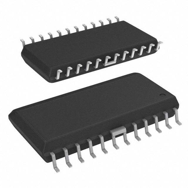
| 描述 | IC MOTOR CONTROLLER PAR 28TSSOP马达/运动/点火控制器和驱动器 Brushless DC Motor Controller |
| 产品分类 | PMIC - 电机, 电桥式驱动器集成电路 - IC |
| 品牌 | Texas Instruments |
| 产品手册 | |
| 产品图片 |
|
| rohs | 符合RoHS无铅 / 符合限制有害物质指令(RoHS)规范要求 |
| 产品系列 | 电源管理 IC,马达/运动/点火控制器和驱动器,Texas Instruments UCC2626PW- |
| 数据手册 | |
| 产品型号 | UCC2626PW |
| 产品 | Brushless DC Motor Controllers |
| 产品种类 | 马达/运动/点火控制器和驱动器 |
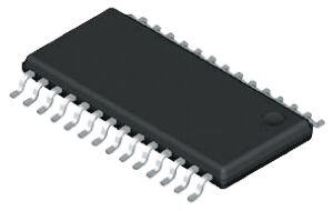
| 供应商器件封装 | 28-TSSOP |
| 其它名称 | 296-34748-5 |
| 功能 | 控制器 - 换向,方向管理 |
| 包装 | 管件 |
| 商标 | Texas Instruments |
| 安装类型 | 表面贴装 |
| 安装风格 | SMD/SMT |
| 封装 | Tube |
| 封装/外壳 | 28-TSSOP(0.173",4.40mm 宽) |
| 封装/箱体 | TSSOP-28 |
| 工作温度 | -40°C ~ 85°C |
| 工作电源电压 | 12.5 V to 20 V |
| 工厂包装数量 | 50 |
| 应用 | 通用 |
| 接口 | 并联 |
| 标准包装 | 50 |
| 电压-电源 | 11 V ~ 14.5 V |
| 电压-负载 | - |
| 电机类型-AC,DC | 无刷 DC(BLDC) |
| 电机类型-步进 | - |
| 电流-输出 | - |
| 电源电流 | 5 mA |
| 类型 | Brushless DC Motor Controller |
| 系列 | UCC2626 |
| 输出配置 | 前级驱动器 |


- 商务部:美国ITC正式对集成电路等产品启动337调查
- 曝三星4nm工艺存在良率问题 高通将骁龙8 Gen1或转产台积电
- 太阳诱电将投资9.5亿元在常州建新厂生产MLCC 预计2023年完工
- 英特尔发布欧洲新工厂建设计划 深化IDM 2.0 战略
- 台积电先进制程称霸业界 有大客户加持明年业绩稳了
- 达到5530亿美元!SIA预计今年全球半导体销售额将创下新高
- 英特尔拟将自动驾驶子公司Mobileye上市 估值或超500亿美元
- 三星加码芯片和SET,合并消费电子和移动部门,撤换高东真等 CEO
- 三星电子宣布重大人事变动 还合并消费电子和移动部门
- 海关总署:前11个月进口集成电路产品价值2.52万亿元 增长14.8%


PDF Datasheet 数据手册内容提取
(cid:1)(cid:2)(cid:2)(cid:3)(cid:4)(cid:3)(cid:4)(cid:5) (cid:1)(cid:2)(cid:2)(cid:7)(cid:4)(cid:3)(cid:4) SLUS318B – APRIL 1999 – REVISED JANUARY 2002 (cid:8)(cid:9)(cid:1)(cid:10)(cid:11)(cid:12)(cid:13)(cid:10)(cid:10) (cid:14)(cid:2) (cid:15)(cid:16)(cid:17)(cid:16)(cid:9) (cid:2)(cid:16)(cid:18)(cid:17)(cid:9)(cid:16)(cid:12)(cid:12)(cid:13)(cid:9) FEATURES voltage- or current-mode configurations. The (cid:1) oscillator is easily synchronized to an external Two-Quadrant and Four-Quadrant Operation master clock source via the SYNCH input. (cid:1) Integrated Absolute Value Current Amplifier Additionally, a QUAD select input configures the (cid:1) Pulse-by-Pulse and Average Current Sensing chip to modulate either the low-side switches only, (cid:1) or both upper and lower switches, allowing the Accurate, Variable Duty-Cycle Tachometer user to minimize switching losses in less Output (cid:1) demanding two-quadrant applications. Trimmed Precision Reference (cid:1) The device includes a differential current-sense Precision Oscillator (cid:1) amplifier and absolute-value circuit which provide Direction Output an accurate reconstruction of motor current, useful for pulse-by-pulse overcurrent protection, as well as closing a current control loop. A DESCRIPTION precision tachometer is also provided for implementing closed-loop speed control. The The UCC3626 motor controller device combines TACH_OUT signal is a variable duty-cycle, many of the functions required to design a frequency output, which can be used directly for high-performance, two- or four-quadrant, three- digital control or filtered to provide an analog phase, brushless dc motor controller into one feedback signal. Other features include COAST, package. Rotor position inputs are decoded to BRAKE, and DIR_IN commands, along with a provide six outputs that control an external power direction output, DIR_OUT. stage. A precision triangle oscillator and latched comparator provide PWM motor control in either (cid:19)(cid:9)(cid:16)(cid:14)(cid:1)(cid:2)(cid:17)(cid:20)(cid:16)(cid:18) (cid:14)(cid:21)(cid:17)(cid:21) (cid:22)(cid:23)(cid:24)(cid:25)(cid:26)(cid:27)(cid:28)(cid:29)(cid:22)(cid:25)(cid:23) (cid:22)(cid:30) (cid:31) (cid:26)(cid:26)!(cid:23)(cid:29) (cid:28)(cid:30) (cid:25)(cid:24) " #$(cid:22)(cid:31)(cid:28)(cid:29)(cid:22)(cid:25)(cid:23) %(cid:28)(cid:29)!& Copyright 2002, Texas Instruments Incorporated (cid:19)(cid:26)(cid:25)% (cid:31)(cid:29)(cid:30) (cid:31)(cid:25)(cid:23)(cid:24)(cid:25)(cid:26)(cid:27) (cid:29)(cid:25) (cid:30)"!(cid:31)(cid:22)(cid:24)(cid:22)(cid:31)(cid:28)(cid:29)(cid:22)(cid:25)(cid:23)(cid:30) "!(cid:26) (cid:29)’! (cid:29)!(cid:26)(cid:27)(cid:30) (cid:25)(cid:24) (cid:17)!((cid:28)(cid:30) (cid:20)(cid:23)(cid:30)(cid:29)(cid:26) (cid:27)!(cid:23)(cid:29)(cid:30) (cid:30)(cid:29)(cid:28)(cid:23)%(cid:28)(cid:26)% )(cid:28)(cid:26)(cid:26)(cid:28)(cid:23)(cid:29)*& (cid:19)(cid:26)(cid:25)% (cid:31)(cid:29)(cid:22)(cid:25)(cid:23) "(cid:26)(cid:25)(cid:31)!(cid:30)(cid:30)(cid:22)(cid:23)+ %(cid:25)!(cid:30) (cid:23)(cid:25)(cid:29) (cid:23)!(cid:31)!(cid:30)(cid:30)(cid:28)(cid:26)(cid:22)$* (cid:22)(cid:23)(cid:31)$ %! (cid:29)!(cid:30)(cid:29)(cid:22)(cid:23)+ (cid:25)(cid:24) (cid:28)$$ "(cid:28)(cid:26)(cid:28)(cid:27)!(cid:29)!(cid:26)(cid:30)& www.ti.com 1
(cid:1)(cid:2)(cid:2)(cid:3)(cid:4)(cid:3)(cid:4)(cid:5) (cid:1)(cid:2)(cid:2)(cid:7)(cid:4)(cid:3)(cid:4) SLUS318B – APRIL 1999 – REVISED JANUARY 2002 AVAILABLE OPTIONS PACKAGED DEVICES TA PDIP SOIC(cid:2) TSSOP(cid:2) (N) (DW) (PW) –40(cid:3)C to 85(cid:3)C UCC2626N UCC2626DW UCC2626PW 0(cid:3)C to 70(cid:3)C UCC3626N UCC3626DW UCC3626PW (cid:2)The DW and PW packages are available taped and reeled. Add TR suffix to device type (e.g. UCC2626DWTR) to order quantities of 2,000 devices per reel. N PACKAGE DW and PW PACKAGES (TOP VIEW) (TOP VIEW) GND 1 28 VDD VREF 2 27 AHI GND 1 28 VDD TACH_OUT 3 26 ALOW VREF 2 27 AHI TACH_OUT 3 26 ALOW R_TACH 4 25 BHI R_TACH 4 25 BHI C_TACH 5 24 BLOW C_TACH 5 24 BLOW CT 6 23 CHI CT 6 23 CHI SYNCH 7 22 CLOW SYNCH 7 22 CLOW DIR_OUT 8 21 DIR_IN DIR_OUT 8 21 DIR_IN SNS_NI 9 20 QUAD SNS_NI 9 20 QUAD SNS_I 10 19 BRAKE SNS_I 10 19 BRAKE IOUT 11 18 COAST IOUT 11 18 COAST OC_REF 12 17 HALLC OC_REF 12 17 HALLC PWM_I 13 16 HALLB PWM_I 13 16 HALLB PWM_NI 14 15 HALLA PWM_NI 14 15 HALLA absolute maximum ratings over operating free-air temperature (unless otherwise noted)† Supply voltage V . . . . . . . . . . . . . . . . . . . . . . . . . . . . . . . . . . . . . . . . . . . . . . . . . . . . . . . . . . . . . . . . . . . . . . . . 15 V DD Input voltage, BRAKE, COAST, DIR_IN, HALLA, HALLB, HALLC, OC_REF, QUAD, SYNCH, PWM_I, PWM_NI . . . . . . . . . . . . . . . . . . . . . . . . . . . –0.3 V to V DD SNS_I, SNS_NI . . . . . . . . . . . . . . . . . . . . . . . . . . . . . . . . . . . . . . . . . . . . . . . . . . . . . –0.5 V to V DD Output current AHI, ALOW, BHI, BLOW, CHI, CLOW . . . . . . . . . . . . . . . . . . . . . . . . . . . . . . . . . . . . . . ±200 mA DIR_OUT, IOUT, TACH_OUT, . . . . . . . . . . . . . . . . . . . . . . . . . . . . . . . . . . . . . . . . . . . . . . . . 1 mA VREF . . . . . . . . . . . . . . . . . . . . . . . . . . . . . . . . . . . . . . . . . . . . . . . . . . . . . . . . . . . . . . . . . . . –20 mA Junction temperature range, T . . . . . . . . . . . . . . . . . . . . . . . . . . . . . . . . . . . . . . . . . . . . . . . . . . . . –55°C to 150°C J Storage temperature range, T . . . . . . . . . . . . . . . . . . . . . . . . . . . . . . . . . . . . . . . . . . . . . . . . . . . . –65°C to 150°C stg Lead temperature soldering 1,6 mm (1/16 inch) from case for 10 seconds . . . . . . . . . . . . . . . . . . . . . . . 300°C †Stresses beyond those listed under “absolute maximum ratings” may cause permanent damage to the device. These are stress ratings only, and functional operation of the device at these or any other conditions beyond those indicated under “recommended operating conditions” is not implied. Exposure to absolute-maximum-rated conditions for extended periods may affect device reliability. ‡All voltages are with respect to GND. Currents are positive into negative out of the specified terminal. 2 www.ti.com
(cid:1)(cid:2)(cid:2)(cid:3)(cid:4)(cid:3)(cid:4)(cid:5) (cid:1)(cid:2)(cid:2)(cid:7)(cid:4)(cid:3)(cid:4) SLUS318B – APRIL 1999 – REVISED JANUARY 2002 block diagram 28 VDD QUAD 20 5 VOLT BRAKE 19 2 VREF REFERENCE COAST 18 1.75V 27 AHI DIR_IN 21 DIRECTION SELECT 25 BHI HALLA 15 HALLB 16 23 CHI HALL DECODER HALLC 17 26 ALOW DIRECTION DIR_OUT 8 DETECTOR EDGE DETECTOR 24 BLOW PWM_NI 14 22 CLOW PWM_I 13 PWM COMPARATOR OSCILLATOR RxC SYNCH 7 S Q 3 TACH_OUT CT 6 R Q OVERCURRENT OC_REF 12 COMPARATOR S Q 5 C_TACH IOUT 11 ONE SENSE AMPLIFIER R Q SHOT 4 R_TACH SNS_NI 9 PWM LOGIC 1 GND SNS_I 10 X5 UDG–97173 www.ti.com 3
(cid:1)(cid:2)(cid:2)(cid:3)(cid:4)(cid:3)(cid:4)(cid:5) (cid:1)(cid:2)(cid:2)(cid:7)(cid:4)(cid:3)(cid:4) SLUS318B – APRIL 1999 – REVISED JANUARY 2002 electrical characteristics over recommended operating conditions, VCC = 12 V; CT = 1 nF, R_TACH = 250 kΩ, C_TACH = 100 pF, T = T , T = –40°C to 85°C for the UCC2626, and 0°C to 70°C A J A for the UCC3626 (unless otherwise noted) overall PARAMETER TEST CONDITIONS MIN TYP MAX UNIT Supply current Outputs not switching 1 3 5 mA undervoltage lockout PARAMETER TEST CONDITIONS MIN TYP MAX UNIT Start threshold 9.0 10.5 11.0 V UVLO hysteresis 0.35 0.40 0.50 V 5-V reference PARAMETER TEST CONDITIONS MIN TYP MAX UNIT Output voltage IVREF = –2 mA 4.9 5 5.1 V Line regulation voltage 11 V < VCC < 14.5 V 10 mV Load regulation voltage –1 mA > IVREF > –5 mA 10 mV Short circuit current 40 120 240 mA coast input comparator PARAMETER TEST CONDITIONS MIN TYP MAX UNIT Threshold voltage 1.60 1.75 2.00 V Hysteresis 0.04 0.10 0.16 V current sense amplifier PARAMETER TEST CONDITIONS MIN TYP MAX UNIT Input offset voltage VCM = 0 V 8 mV Input bias current VCM = 0 V 5 10 15 µA Gain VCM = 0 V 4.85 5.00 5.15 V/V PSRR 11 V < VCC < 14.5 V 60 dB High-level output voltage IIOUT= –100 µA 6.3 V Low-level output voltage IIOUT = 100 µA 70 mV UCC3626 VIOUT = 2 V 500 µA OOuuttppuutt ssoouurrccee ccuurrrreenntt UCC2626 VIOUT = 2 V 300 µA pwm comparator PARAMETER TEST CONDITIONS MIN TYP MAX UNIT Input common mode range 2.0 8.0 V Propagation delay time 75 150 ns overcurrent comparator PARAMETER TEST CONDITIONS MIN TYP MAX UNIT Input common mode range 0.0 5.0 V Propagation delay time 50 175 250 ns logic inputs PARAMETER TEST CONDITIONS MIN TYP MAX UNIT High-level logic input voltage QUAD, BRAKE, DIR, SYNCH 3.6 V Low-level logic input voltage QUAD, BRAKE, DIR, SYNCH 1.4 V 4 www.ti.com
(cid:1)(cid:2)(cid:2)(cid:3)(cid:4)(cid:3)(cid:4)(cid:5) (cid:1)(cid:2)(cid:2)(cid:7)(cid:4)(cid:3)(cid:4) SLUS318B – APRIL 1999 – REVISED JANUARY 2002 electrical characteristics over recommended operating conditions, VCC = 12 V; CT = 1 nF, R_TACH = 250 kΩ, C_TACH = 100 pF, T = T , T = –40°C to 85°C for the UCC2626, and 0°C to 70°C A J A for the UCC3626 (unless otherwise noted) hall buffer inputs PARAMETER TEST CONDITIONS MIN TYP MAX UNIT High-level input voltage HALLA, HALLB, HALLC 1.7 1.9 2.1 V Hysteresis HALLA, HALLB, HALLC 0.6 1.0 V Input current 0V < VIN < 5 V –25 µA oscillator PARAMETER TEST CONDITIONS MIN TYP MAX UNIT Frequency RTACH = 250 kΩ, CT = 1nF 9.0 10.0 11.0 kHz Frequency change with voltage 12 V < VCC < 14.5 V 3% CT peak voltage 7.25 7.5 7.75 V CT peak-to-valley voltage 4.75 5.0 5.25 V SYNCH pin minimum pulse width 500 ns tachometer PARAMETER TEST CONDITIONS MIN TYP MAX UNIT High-level output voltage/VREF IOUT = –10 µA 99% 100% Low-level output voltage IOUT = 10 µA 0 20 mV High-level on-resistance IOUT = –100 µA 1 1.5 kΩ Low-level on-resistance IOUT = 100 µA 1 1.5 kΩ High-level ramp threshold voltage 2.5 V Ramp voltage 2.375 2.500 2.625 V CTACH charge current RTACH = 49.9 kΩ 48 51 53 µA UCC3626 See Note 1 –3% 3% OOnn-ttiimmee aaccccuurraaccyy UCC2626 See Note 1 –4% 3% direction output PARAMETER TEST CONDITIONS MIN TYP MAX UNIT High-level output voltage IOUT = –100 µA 4.5 5.2 V Low-level output voltage IOUT = 100 µA 0 0.5 V output PARAMETER TEST CONDITIONS MIN TYP MAX UNIT Maximum duty cycle 100% IOUT = 2 mA 0.0 0.1 0.5 V LLoow-lleeveell oouttpputt voollttaaggee IOUT = 100 µA 0.0 0.1 V IOUT = –2 mA 4.0 4.8 5.2 V HHiigghh-lleevveell oouuttppuutt vvoollttaaggee IOUT = –100 µA 4.7 5.2 V Rise and fall time CI = 10 pF 100 ns (cid:3) (cid:5) C (cid:2) V (cid:4)V NOTE 1: tON is calculated using the formula tON(cid:1) TACHI HI LO CHARGE www.ti.com 5
(cid:1)(cid:2)(cid:2)(cid:3)(cid:4)(cid:3)(cid:4)(cid:5) (cid:1)(cid:2)(cid:2)(cid:7)(cid:4)(cid:3)(cid:4) SLUS318B – APRIL 1999 – REVISED JANUARY 2002 pin descriptions AHI, BHI, CHI: Digital outputs used to control the high-side switches in a three-phase inverter. For specific decoding information reference Table I. ALOW, BLOW, CLOW: Digital outputs used to control the low-side switches in a three-phase inverter. For specific decoding information reference Table I. BRAKE: BRAKE is a digital input which causes the device to enter brake mode. In brake mode all three high- side outputs (AHI, BHI & CHI) are turned off, while all three lowside outputs (ALOW, BLOW, CLOW) are turned on. During brake mode the tachometer output remains operational. The only conditions that can inhibit the low-side commands during brake are UVLO, exceeding peak current, the output of the PWM comparator, or the COAST command. COAST: The COAST input consists of a hysteretic comparator which disables the outputs. The input is useful in implementing an overvoltage bus clamp in four-quadrant applications. The outputs are disabled when the input is above 1.75 V. CT: This pin is used in conjunction with the R_TACH pin to set the frequency of the oscillator. A timing capacitor is normally connected between this point and ground and is alternately charged and discharged between 2.5 V and 7.5 V. C_TACH: A timing capacitor is connected between this pin and ground to set the width of the TACH_OUT pulse. The capacitor is charged with a current set by the resistor on pin R_TACH . DIR_IN: DIR_IN is a digital input which determines the order in which the HALLA, HALLB, and HALLC inputs are decoded. For specific decode information reference Table I. DIR_OUT: DIR_OUT represents the actual direction of the rotor as decoded from the HALLA, HALLB, and HALLC inputs. For any valid combination of HALLA, HALLB, and HALLC inputs there are two valid transitions; one of which translates to a clockwise rotation and another which translates to a counterclockwise rotation. The polarity of DIR_OUT is the same as DIR_IN while motoring, (i.e. sequencing from top to bottom in Table 1.) GND: GND is the reference ground for all functions of the part. Bypass and timing capacitors should be terminated as close as possible to this point. HALLA, HALLB, HALLC: These three inputs are designed to accept rotor position information positioned 120° apart. For specific decode information reference Table I. These inputs should be externally pulled up to VREF or another appropriate external supply. IOUT: IOUT represents the output of the current sense and absolute value amplifiers. The output signal appearing is a representation of the following expression: (cid:3) (cid:5) I (cid:1)ABS I (cid:4)I (cid:2)5 OUT SNS_I SNS_NI This output can be used to close a current control loop as well as provide additional filtering of the current sense signal. OC_REF: OC_REF is an analog input which sets the trip voltage of the overcurrent comparator. The sense input of the comparator is internally connected to the output of the current sense amplifier and absolute value circuit. PWM_NI: PWM_NI is the noninverting input to the PWM comparator. PWM_I: PWM_I is the inverting input to the PWM comparator. QUAD: The QUAD input selects between two-quadrant operation (QUAD = 0) and four-quadrant operation (QUAD = 1) . When in two-quadrant mode, only the low-side devices are effected by the output of the PWM comparator. In four-quadrant mode both high- and low-side devices are controlled by the PWM comparator. 6 www.ti.com
(cid:1)(cid:2)(cid:2)(cid:3)(cid:4)(cid:3)(cid:4)(cid:5) (cid:1)(cid:2)(cid:2)(cid:7)(cid:4)(cid:3)(cid:4) SLUS318B – APRIL 1999 – REVISED JANUARY 2002 pin descriptions SYNCH: The SYNCH input is used to synchronize the PWM oscillator with an external digital clock. When using the SYNCH feature, a resistor equal to R_TACH must be placed in parallel with CT. When not using the SYNCH feature, SYNCH must be grounded. SNS_NI, SNS_I: These inputs are the noninverting and inverting inputs to the current sense amplifier, respectively. The integrated amplifier is configured for a gain of five. An absolute value function is also incorporated into the output in order to provide a representation of actual motor current when operating in four-quadrant mode. TACH_OUT: TACH_OUT is the output of a monostable triggered by a change in the commutation state, thus providing a variable duty cycle, frequency output. The on time of the monostable is set by the timing capacitor connected to C_TACH. The monostable is capable of being retriggered if a commutation occurs during its on-time. R_TACH: A resistor connected between R_TACH and ground programs the current for both the oscillator and tachometer. VDD: VDD is the input supply connection for this device. Undervoltage lockout keeps the outputs off for inputs below 10.5 V. The input should be bypassed with a 0.1-µF ceramic capacitor, minimum. VREF: VREF is a 5-V, 2% trimmed reference output with 5 mA of maximum available output current. This pin should be bypassed to ground with a ceramic capacitor with a value of at least 0.1 µF. APPLICATION INFORMATION Table 1 provides the decode logic for the six outputs, AHI, BHI, CHI, ALOW, BLOW, and CLOW as a function of the BRAKE, COAST, DIR_IN, HALLA, HALLB, and HALLC inputs. Table 1. Commutation Truth Table HALL HIGH-SIDE LOW-SIDE BBRRAAKKEE CCOOAASSTT DDIIRR__IINN INPUTS OUTPUTS OUTPUTS A B C A B C A B C 0 0 1 1 0 1 1 0 0 0 1 0 0 0 1 1 0 0 1 0 0 0 0 1 0 0 1 1 1 0 0 1 0 0 0 1 0 0 1 0 1 0 0 1 0 1 0 0 0 0 1 0 1 1 0 0 1 1 0 0 0 0 1 0 0 1 0 0 1 0 1 0 0 0 0 1 0 1 0 1 0 1 0 0 0 0 0 0 0 1 0 1 0 0 0 1 0 0 0 0 1 1 1 0 0 0 0 1 0 0 0 0 1 0 1 0 0 0 1 0 0 0 0 1 1 0 0 0 1 0 1 0 0 0 0 1 0 0 0 0 1 1 0 0 X 1 X X X X 0 0 0 0 0 0 1 0 X X X X 0 0 0 1 1 1 0 0 X 1 1 1 0 0 0 0 0 0 0 0 X 0 0 0 0 0 0 0 0 0 www.ti.com 7
(cid:1)(cid:2)(cid:2)(cid:3)(cid:4)(cid:3)(cid:4)(cid:5) (cid:1)(cid:2)(cid:2)(cid:7)(cid:4)(cid:3)(cid:4) SLUS318B – APRIL 1999 – REVISED JANUARY 2002 APPLICATION INFORMATION The UCC3626 is designed to operate with 120° position sensor encoding. In this format, the three position sensor signals are never simultaneously high or low. Motors whose sensors provide 60° encoding, can be converted to 120° using the circuit shown in Figure 1. In order to prevent noise from commanding improper commutation states, some form of low-pass filtering on HALLA, HALLB, and HALLC is recommended. Passive RC networks generally work well and should be located as close as possible to the device. Figure 2 illustrates these techniques. VREF VREF 1 kΩ 499 Ω 1 kΩ HALLB 499 Ω HALLA HALLA HALLA 2.2 nF 2.2 nF VREF 1 kΩ VREF HALLA 1 kΩ 1 kΩ 499 Ω 2N2222A HALLB HALLB HALLB 2.2 nF 2.2 nF VREF VREF 1 kΩ 499 Ω 1 kΩ 499 Ω HALLC HALLC HALLC HALLC 2.2 nF 2.2 nF UDG–97182 UDG–97185 Figure 1. Converting Hall Code From 60° to 120° Figure 2. Passive Hall Filtering Technique 8 www.ti.com
(cid:1)(cid:2)(cid:2)(cid:3)(cid:4)(cid:3)(cid:4)(cid:5) (cid:1)(cid:2)(cid:2)(cid:7)(cid:4)(cid:3)(cid:4) SLUS318B – APRIL 1999 – REVISED JANUARY 2002 APPLICATION INFORMATION configuring the oscillator The UCC3626 oscillator is designed to operate at frequencies up to 250 kHz and provide a triangle waveform on CT with a peak-to-peak amplitude of 5 V for improved noise immunity. The current used to program CT is derived from the R_TACH resistor according to the following equation: I (cid:1) 25 Amps OSC R_TACH (1) The oscillator frequency is set by R_TACH and CT according to the following relationship: f (cid:1) 2.5 Hz OSC R_TACH(cid:2)CT (2) Timing resistor values should be between 25 kΩ and 500 kΩ, while capacitor values should be between 100 pF and 1 µF. Figure 3 provides a graph of oscillator frequency for various combinations of timing components. As with any high-frequency oscillator, timing components should be located as close as possible to the device pins when laying out the printed-circuit board. It is also important to reference the timing capacitor directly to the ground pin on the UCC3626 rather than daisy chaining it to another trace or the ground plane. This technique prevents switching current spikes in the local ground from causing jitter in the oscillator. synchronizing the oscillator A common system specification is to have all oscillators synchronized to a master clock. The UCC3626 provides a SYNCH input for this purpose. The SYNCH input is designed to interface with a digital clock pulse generated by the master oscillator. A positive-going edge on this input causes the UCC3626 oscillator to begin discharging. In order for the slave oscillator to function properly, it must be programmed for a frequency slightly lower than that of the master. Also, a resistor equal to R_TACH must be placed in parallel with CT. Figure 4 illustrates the waveforms for a slave oscillator programmed to 20 kHz with a master frequency of 30 kHz. The SYNCH pin must be grounded when not used. OSCILLATOR FREQUENCY vs TIMING CAPACITANCE 1.E+06 R_TACH = 25 kΩ z H y – 1.E+05 R_TACH = 100 kΩ c n e u q e r F M W P – 1.E+04 C S O f R_TACH = 250 kΩ R_TACH = 500 kΩ 1.E+03 1.E–10 1.E–09 1.E–08 1.E–07 CT – Oscillator Timing Capacitance – F Figure 3 www.ti.com 9
(cid:1)(cid:2)(cid:2)(cid:3)(cid:4)(cid:3)(cid:4)(cid:5) (cid:1)(cid:2)(cid:2)(cid:7)(cid:4)(cid:3)(cid:4) SLUS318B – APRIL 1999 – REVISED JANUARY 2002 APPLICATION INFORMATION programming the tachometer The UCC3626 tachometer consists of a precision 5-V monostable, triggered by either a rising or falling edge on any of the three Hall inputs, HALLA, HALLB, and HALLC. The resulting TACH_OUT waveform is a variable duty-cycle square wave whose frequency is proportional to motor speed, as given by: TACH_OUT(cid:1)V(cid:2)P Hz 20 (3) where P is the number of motor pole pairs and V is motor velocity in RPM. The on time of the monostable is programmed via timing resistor R_TACH and capacitor C_TACH according to the following equation: t (cid:1)R_TACH(cid:2)C_TACH sec ON (4) Figure 5 provides a graph of on times for various combinations of R_TACH and C_TACH. On time is typically set to a value less than the minimum TACH_OUT period as given by: t (cid:1) 20 sec PERIOD(min) V (cid:2)P MAX (5) where P is the number of motor pole pairs and V is motor velocity in RPM. TACHOMETER ON-TIME vs TIMING CAPACITANCE 1.E+00 R_TACH = 500 kΩ s 1.E–01 – e m Ti n– 1.E–02 R_TACH = 250 kΩ O r e SYNCH met 1.E–03 o h WITHOUT SYNCH ac R_TACH = 100 kΩ T – 1.E–04 N O t CT 1.E–05 WITH SYNCH R_TACH = 25 kΩ 1.E–06 1.E–10 1.E–09 1.E–08 1.E–07 1.E–06 C_TACH – Tachometer Timing Capacitance – F Figure 4. Oscillator Waveforms Figure 5 10 www.ti.com
(cid:1)(cid:2)(cid:2)(cid:3)(cid:4)(cid:3)(cid:4)(cid:5) (cid:1)(cid:2)(cid:2)(cid:7)(cid:4)(cid:3)(cid:4) SLUS318B – APRIL 1999 – REVISED JANUARY 2002 APPLICATION INFORMATION The TACH_OUT signal can be used to close a digital velocity loop using a microcontroller, as shown in Figure 6, or directly low-pass filtered in an analog implementation, Figure 7. UCC3626 4 R_TACH MC68HC11 AD558 5 C_TACH PB0–PB7 DB0–DB7 6 CT PC0 VCE 14 PWM_NI VCS VOUT 13 PWM_I VOUTSENSE VOUTSELECT IC1 3 TACH_OUT UDG–97188 Figure 6. Digital Velocity Loop Implementation Using MC68HC11 two quadrant vs four quadrant control Figure 8 illustrates the four possible quadrants of operation for a motor. Two-quadrant control refers to a system in which operation is limited to quadrants I and III (where torque and velocity are in the same direction). With a two-quadrant brushless dc amplifier, there are no provisions other than friction to decelerate the load, limiting the approach to less demanding applications. Four-quadrant controllers, on the other hand, provide controlled operation in all quadrants, including II and IV, where torque and rotation are of opposite direction. UCC3626 VELOCITY CW 2 VREF 4 R_TACH 5 C_TACH II I 6 CT TORQUE CCW CW 14 PWM_NI III IV – 13 PWM_I + 3 TACH_OUT CCW UDG–97189 UDG–01118 Figure 7. Simple Analog Velocity Loop Figure 8. Four Quadrants of Operation www.ti.com 11
(cid:1)(cid:2)(cid:2)(cid:3)(cid:4)(cid:3)(cid:4)(cid:5) (cid:1)(cid:2)(cid:2)(cid:7)(cid:4)(cid:3)(cid:4) SLUS318B – APRIL 1999 – REVISED JANUARY 2002 APPLICATION INFORMATION When configured for two-quadrant operation, (QUAD=0), the UCC3626 modulates only the low-side devices of the output power stage. The current paths within the output stage during the PWM on- and off-times are illustrated in Figure 9. During the on interval, both switches are on, and current flows through the load down to ground. During the off time, the lower switch is shut off, and the motor current circulates through the upper half bridge via the flyback diode. The motor is assumed to be operating in either quadrant I or III. If operation is attempted in quadrants II or IV by changing the DIR bit and reversing the torque, switches 1 and 4 are turned off and switches 2 and 3 turned on. Under this condition motor current very quickly decays, reverses direction and increases until the control threshold is reached. At this point, switch 2 turns off and current once again circulates in the upper half bridge. However, in this case, the motor’s BEMF is in phase with the current, (i.e. the motor’s direction of rotation has not yet changed.) Figure 10 illustrates the current paths when operating in this mode. Under these conditions there is nothing to limit the current other than motor and drive impedance. These high-circulating currents can result in damage to the power devices in addition to high, uncontrolled torque. VMOT VMOT S1 S3 S5 S1 S3 S5 IOFF IOFF IPHASE IPHASE + BEMF – + BEMF – ION ION S2 S4 S6 S2 S4 S6 UDG–01119 UDG–01120 Figure 9. Two-Quadrant Chopping Figure 10. Two-Quadrant Reversal 12 www.ti.com
(cid:1)(cid:2)(cid:2)(cid:3)(cid:4)(cid:3)(cid:4)(cid:5) (cid:1)(cid:2)(cid:2)(cid:7)(cid:4)(cid:3)(cid:4) SLUS318B – APRIL 1999 – REVISED JANUARY 2002 APPLICATION INFORMATION By pulse width modulating both the upper and lower power devices (QUAD=1), motor current always decays during the PWM off time, eliminating any uncontrolled circulating currents. In addition, current always flows through the current sense resistor, providing a suitable feedback signal. Figure 11 illustrates the current paths during a four-quadrant torque reversal. Motor drive waveforms for both two- and four-quadrant operation are illustrated in Figure 12. VMOT S1 S3 S5 IPHASE + BEMF – IOFF ION S2 S4 S6 UDG–01121 Figure 11. Four-Quadrant Reversal www.ti.com 13
(cid:1)(cid:2)(cid:2)(cid:3)(cid:4)(cid:3)(cid:4)(cid:5) (cid:1)(cid:2)(cid:2)(cid:7)(cid:4)(cid:3)(cid:4) SLUS318B – APRIL 1999 – REVISED JANUARY 2002 APPLICATION INFORMATION ROTOR POSITION IN ELECTRICAL DEGREES 0 60 120 180 240 300 360 420 480 540 600 660 720 H1 SENSOR INPUTS H2 H3 Code 101 100 110 010 011 001 101 100 110 010 011 001 HIGH SIDE AHI OUTPUTS BHI QUAD=0 CHI ALO LOW SIDE OUTPUTS BLO QUAD=0 CLO + A 0 – + MOTOR PHASE CURRENTSB 0 QUAD=0 – + C 0 – HIGH SIDEAHI OUTPUTS BHI QUAD=1 CHI ALO LOW SIDE OUTPUTS BLO QUAD=1 CLO + A 0 – + MOTOR PHASE CURRENTSB 0 QUAD=1 – + C 0 – 100% Duty Cycle PWM 50% Duty Cycle PWM UDG–97190 Figure 12. Motor Drive and Current Waveforms for Two-Quadrant (QUAD=0) and Four-Quadrant (QUAD=1) Operation 14 www.ti.com
(cid:1)(cid:2)(cid:2)(cid:3)(cid:4)(cid:3)(cid:4)(cid:5) (cid:1)(cid:2)(cid:2)(cid:7)(cid:4)(cid:3)(cid:4) SLUS318B – APRIL 1999 – REVISED JANUARY 2002 APPLICATION INFORMATION power stage design considerations The flexible architecture of the UCC3626 requires the user to pay close attention to the design of the power output stage. Two- and four-quadrant applications not requiring the brake function are able to use the power stage approach illustrated in Figure 13a. In many cases the body diode of the MOSFET can be used to reduce parts count and cost. If efficiency is a key requirement, Schottky diodes can be used in parallel with the switches. UDG–97190 VMOT VMOT VMOT TO TO TO MOTOR MOTOR MOT CURRENT CURRENT CURRENT SENSE SENSE SENSE (a) (b) (c) UDG–01122 CURRENT SENSE TTWWOO FFOOUURR SSAAFFEE PPOOWWEERR PULSE-BY- QUADRANT QUADRANT BRAKING REVERSAL AVERAGE PULSE (a) YES YES NO Four-Quad Only YES YES (b) YES NO YES No YES NO (c) YES YES YES Four-Quad Only YES YES Figure 13. Power Stage Topologies If the system requires a braking function, diodes must be added in series with the lower power devices and the lower flyback diodes must be returned to ground, as pictured in Figure 13b, and 13c. This requirement prevents brake currents from circulating in the lower half bridge and bypassing the sense resistor. In addition, the combination of braking and four-quadrant control necessitates an additional resistor in the diode path to sense current during the PWM off time as illustrated in Figure 13c. www.ti.com 15
(cid:1)(cid:2)(cid:2)(cid:3)(cid:4)(cid:3)(cid:4)(cid:5) (cid:1)(cid:2)(cid:2)(cid:7)(cid:4)(cid:3)(cid:4) SLUS318B – APRIL 1999 – REVISED JANUARY 2002 APPLICATION INFORMATION current sensing The UCC3626 includes a differential current-sense amplifier with a fixed gain of five, along with an absolute value circuit. The current-sense signal should be low pass filtered to eliminate leading-edge spikes. In order to maximize performance, the input impedance of the amplifier should be balanced. If the sense voltage must be trimmed for accuracy reasons, a low-value input divider or a differential divider should be used to maintain impedance matching, as shown in Figure 14. RF RF SNS_NI SNS_NI RF RADJ RADJ RS CF RS CF RF RF SNS_I SNS_I RADJ << RF (a) (b) UDG–01123 Figure 14. (a) Differential Divider and (b) Low-Value Divider With four-quadrant chopping, motor current always flows through the sense resistor. However, during the flyback period the polarity across the sense resistor is reversed. The absolute value amplifier cancels the polarity reversal by inverting the negative sense signal during the flyback time, see Figure 15. Therefore, the output of the absolute value amplifier is a reconstructed analog of the motor current, suitable for protection as well as feedback loop closure. VMOT Ip Is S1 S3 S5 IPHASE Ip If + BEMF – IOFF 5*Ip ION S2 S4 S6 Im Is X5 Im UDG–01124 If Figure 15. Current Sense Amplifier Waveform 16 www.ti.com
(cid:1)(cid:2)(cid:2)(cid:3)(cid:4)(cid:3)(cid:4)(cid:5) (cid:1)(cid:2)(cid:2)(cid:7)(cid:4)(cid:3)(cid:4) SLUS318B – APRIL 1999 – REVISED JANUARY 2002 APPLICATION INFORMATION Figure 17 illustrates a simple 175-V, 2-A, two-quadrant velocity controller using the UCC3626. The power stage is designed to operate with a rectified off-line supply using IR2210s to provide the interface between the low voltage control signals and the power MOSFETs. The power topology illustrated in Figure 13c is implemented in order to provide braking capability. SIGN/MAGNITUDE CONVERTER 11 IOUT 10 kΩ 10 kΩ 10 kΩ 10 kΩ – – U1 U5 VELOCITY + + – COM±5M VAND 10 kΩ –U6 +U8 13 PWM_I + CURRENT CURRENT ERROR MAGNITUDE AMPLIFIER U7 21 DIR CURRENT SIGN BIPOLAR 10 kΩ TACH GAIN 10 kΩ U3– 4.99 kΩ 4.99 kΩ – TACFHIOLTMEERTER + U2 + 3 TACH_OUT 2N7002 8 DIR_OUT UDG–99061 Figure 16. Four-Quadrant Control Loop The controller’s speed command is set by potentiometer R30, while the speed feedback signal is obtained by low-pass filtering and buffering the TACH_OUT signal using R11 and C9. Small signal compensation of the velocity control loop is provided by amplifier U5A, whose output is used to control the PWM duty cycle. The integrating capacitor, C8, places a pole at 0 Hz and a zero in conjunction with R10. This zero can be used to cancel the low-frequency motor pole and to cross the loop-over with a –20 dB gain response. Four-quadrant applications require the control of motor current. Figure 16 illustrates a sign/magnitude current control loop within an outer bipolar velocity loop using the UCC3626. U1 serves as the velocity loop error amplifier and accepts a ±5-V command signal. Velocity feedback is provided by low-pass filtering and scaling the TACH_OUT signal using U2. The direction output switch, DIR_OUT, and U3 set the polarity of the tachometer gain according to the direction of rotation. The output of the velocity error amplifier, U1, is then converted to sign/magnitude form using U5 and U6. The sign portion is used to drive the DIR input while the magnitude commands the current error amplifier, U8. Current feedback is provided by the internal current sense amplifier via the IOUT pin. www.ti.com 17
(cid:1)(cid:2)(cid:2)(cid:3)(cid:4)(cid:3)(cid:4)(cid:5) (cid:1)(cid:2)(cid:2)(cid:7)(cid:4)(cid:3)(cid:4) SLUS318B – APRIL 1999 – REVISED JANUARY 2002 APPLICATION INFORMATION C22µ10 F MOTORPHASE A D81N5418 C21µ10 F MOTORPHASE B D111N5418 C20µ10 F MOTORPHASE C D151N5418 R28Ω0.1 OT Q1IRF730 D7MUR1520 Q2IRF730 OT Q3IRF730 D10MUR1520 Q4IRF730 OT Q5IRF730 D13MUR1520 Q2IRF730 R27Ω0.1 M M M V V V D1R15Ω1N414810 R16Ω47 C12µ0.1 F +12VD1611DF4 R17D2Ω101N4148C13µ0.1 FR18Ω47 D3R19Ω1N414810 R20Ω47 C15µ0.1 F D17+12V11DF4 R21D4Ω101N4148C16µ0.1 FR22Ω47 D5R23Ω1N414810 R24Ω47 C18µ0.1 F +12VD1811DF4 R25D6Ω101N4148C19µ0.1 FR18Ω47 ΩR30 2 k ΩR31 2 k 6 7 5 4 3 2 1 6 7 5 4 3 2 1 6 7 5 4 3 2 1 B O S C C M O B O S C C M O B O S C C M O V H V N C O L V H V N C O L V H V N C O L U2 IR2110VDD NC HIN LIN SDV NCC VSS U3 IR2110VDD NC HIN LIN SDV NCC VSS U3 IR2110VDD NC HIN LIN SDV NCC VSS C23µ0.1 F 9 8 10 12 11 14 13 9 8 10 12 11 14 13 9 8 10 12 11 14 13 F C11µ0.1 F F C14µ0.1 F F C17µ0.1 F E E E R R R V V V C103900 pF R12Ω250 k VREF R13Ω35 k R14Ω15 k 27 25 23 26 24 22 9 10 12 5 11 4 3 8 U1 CC3626AHI BHI CHI ALOW BLOW CLOW SNS_NI SNS_I OC_REF CTACH IOUT RTACH TACH_OUT DIR_OUT R11Ω160 k C9µ0.1 F U28VDD 2VREF F1GND 15HALLA 16HALLB 17HALLC 20QUAD 21DIR_IN 19BRAKE 18COAST 7SYNCH 6CT 14PWN_IN 13PWM_I U5B1/2 LM358 + F C1µ0.1 VREF+12V R2R3VREC2ΩΩ1 k1 kµ0.1 FR4 Ω499R5C3Ω4992200 pFC4C52200 pF2200 pFVREF R9R8R7ΩΩΩ10 k10 k10 k C6100 pF C7 R10C8REF +U5A1/2 LM358SPEED SET R29 R1Ω1 k R6Ω499 V R30Ω10 k S FROMHALLSENSOR UDG–01117 Figure 17. Two-Quadrant Velocity Controller 18 www.ti.com
PACKAGE OPTION ADDENDUM www.ti.com 24-Aug-2018 PACKAGING INFORMATION Orderable Device Status Package Type Package Pins Package Eco Plan Lead/Ball Finish MSL Peak Temp Op Temp (°C) Device Marking Samples (1) Drawing Qty (2) (6) (3) (4/5) UCC2626DW ACTIVE SOIC DW 28 20 Green (RoHS CU NIPDAU Level-2-260C-1 YEAR -40 to 85 UCC2626DW & no Sb/Br) UCC2626PW ACTIVE TSSOP PW 28 50 Green (RoHS CU NIPDAU Level-2-260C-1 YEAR -40 to 85 UCC2626PW & no Sb/Br) UCC2626PWG4 ACTIVE TSSOP PW 28 50 Green (RoHS CU NIPDAU Level-2-260C-1 YEAR -40 to 85 UCC2626PW & no Sb/Br) UCC3626DW ACTIVE SOIC DW 28 20 Green (RoHS CU NIPDAU Level-2-260C-1 YEAR 0 to 70 UCC3626DW & no Sb/Br) UCC3626DWTR ACTIVE SOIC DW 28 1000 Green (RoHS CU NIPDAU Level-2-260C-1 YEAR 0 to 70 UCC3626DW & no Sb/Br) UCC3626PW ACTIVE TSSOP PW 28 50 Green (RoHS CU NIPDAU Level-2-260C-1 YEAR 0 to 70 UCC3626PW & no Sb/Br) (1) The marketing status values are defined as follows: ACTIVE: Product device recommended for new designs. LIFEBUY: TI has announced that the device will be discontinued, and a lifetime-buy period is in effect. NRND: Not recommended for new designs. Device is in production to support existing customers, but TI does not recommend using this part in a new design. PREVIEW: Device has been announced but is not in production. Samples may or may not be available. OBSOLETE: TI has discontinued the production of the device. (2) RoHS: TI defines "RoHS" to mean semiconductor products that are compliant with the current EU RoHS requirements for all 10 RoHS substances, including the requirement that RoHS substance do not exceed 0.1% by weight in homogeneous materials. Where designed to be soldered at high temperatures, "RoHS" products are suitable for use in specified lead-free processes. TI may reference these types of products as "Pb-Free". RoHS Exempt: TI defines "RoHS Exempt" to mean products that contain lead but are compliant with EU RoHS pursuant to a specific EU RoHS exemption. Green: TI defines "Green" to mean the content of Chlorine (Cl) and Bromine (Br) based flame retardants meet JS709B low halogen requirements of <=1000ppm threshold. Antimony trioxide based flame retardants must also meet the <=1000ppm threshold requirement. (3) MSL, Peak Temp. - The Moisture Sensitivity Level rating according to the JEDEC industry standard classifications, and peak solder temperature. (4) There may be additional marking, which relates to the logo, the lot trace code information, or the environmental category on the device. (5) Multiple Device Markings will be inside parentheses. Only one Device Marking contained in parentheses and separated by a "~" will appear on a device. If a line is indented then it is a continuation of the previous line and the two combined represent the entire Device Marking for that device. Addendum-Page 1
PACKAGE OPTION ADDENDUM www.ti.com 24-Aug-2018 (6) Lead/Ball Finish - Orderable Devices may have multiple material finish options. Finish options are separated by a vertical ruled line. Lead/Ball Finish values may wrap to two lines if the finish value exceeds the maximum column width. Important Information and Disclaimer:The information provided on this page represents TI's knowledge and belief as of the date that it is provided. TI bases its knowledge and belief on information provided by third parties, and makes no representation or warranty as to the accuracy of such information. Efforts are underway to better integrate information from third parties. TI has taken and continues to take reasonable steps to provide representative and accurate information but may not have conducted destructive testing or chemical analysis on incoming materials and chemicals. TI and TI suppliers consider certain information to be proprietary, and thus CAS numbers and other limited information may not be available for release. In no event shall TI's liability arising out of such information exceed the total purchase price of the TI part(s) at issue in this document sold by TI to Customer on an annual basis. Addendum-Page 2
PACKAGE MATERIALS INFORMATION www.ti.com 14-Jul-2012 TAPE AND REEL INFORMATION *Alldimensionsarenominal Device Package Package Pins SPQ Reel Reel A0 B0 K0 P1 W Pin1 Type Drawing Diameter Width (mm) (mm) (mm) (mm) (mm) Quadrant (mm) W1(mm) UCC3626DWTR SOIC DW 28 1000 330.0 32.4 11.35 18.67 3.1 16.0 32.0 Q1 PackMaterials-Page1
PACKAGE MATERIALS INFORMATION www.ti.com 14-Jul-2012 *Alldimensionsarenominal Device PackageType PackageDrawing Pins SPQ Length(mm) Width(mm) Height(mm) UCC3626DWTR SOIC DW 28 1000 367.0 367.0 55.0 PackMaterials-Page2
IMPORTANTNOTICE TexasInstrumentsIncorporated(TI)reservestherighttomakecorrections,enhancements,improvementsandotherchangestoits semiconductorproductsandservicesperJESD46,latestissue,andtodiscontinueanyproductorserviceperJESD48,latestissue.Buyers shouldobtainthelatestrelevantinformationbeforeplacingordersandshouldverifythatsuchinformationiscurrentandcomplete. TI’spublishedtermsofsaleforsemiconductorproducts(http://www.ti.com/sc/docs/stdterms.htm)applytothesaleofpackagedintegrated circuitproductsthatTIhasqualifiedandreleasedtomarket.AdditionaltermsmayapplytotheuseorsaleofothertypesofTIproductsand services. ReproductionofsignificantportionsofTIinformationinTIdatasheetsispermissibleonlyifreproductioniswithoutalterationandis accompaniedbyallassociatedwarranties,conditions,limitations,andnotices.TIisnotresponsibleorliableforsuchreproduced documentation.Informationofthirdpartiesmaybesubjecttoadditionalrestrictions.ResaleofTIproductsorserviceswithstatements differentfromorbeyondtheparametersstatedbyTIforthatproductorservicevoidsallexpressandanyimpliedwarrantiesforthe associatedTIproductorserviceandisanunfairanddeceptivebusinesspractice.TIisnotresponsibleorliableforanysuchstatements. BuyersandotherswhoaredevelopingsystemsthatincorporateTIproducts(collectively,“Designers”)understandandagreethatDesigners remainresponsibleforusingtheirindependentanalysis,evaluationandjudgmentindesigningtheirapplicationsandthatDesignershave fullandexclusiveresponsibilitytoassurethesafetyofDesigners'applicationsandcomplianceoftheirapplications(andofallTIproducts usedinorforDesigners’applications)withallapplicableregulations,lawsandotherapplicablerequirements.Designerrepresentsthat,with respecttotheirapplications,Designerhasallthenecessaryexpertisetocreateandimplementsafeguardsthat(1)anticipatedangerous consequencesoffailures,(2)monitorfailuresandtheirconsequences,and(3)lessenthelikelihoodoffailuresthatmightcauseharmand takeappropriateactions.DesigneragreesthatpriortousingordistributinganyapplicationsthatincludeTIproducts,Designerwill thoroughlytestsuchapplicationsandthefunctionalityofsuchTIproductsasusedinsuchapplications. TI’sprovisionoftechnical,applicationorotherdesignadvice,qualitycharacterization,reliabilitydataorotherservicesorinformation, including,butnotlimitedto,referencedesignsandmaterialsrelatingtoevaluationmodules,(collectively,“TIResources”)areintendedto assistdesignerswhoaredevelopingapplicationsthatincorporateTIproducts;bydownloading,accessingorusingTIResourcesinany way,Designer(individuallyor,ifDesignerisactingonbehalfofacompany,Designer’scompany)agreestouseanyparticularTIResource solelyforthispurposeandsubjecttothetermsofthisNotice. TI’sprovisionofTIResourcesdoesnotexpandorotherwisealterTI’sapplicablepublishedwarrantiesorwarrantydisclaimersforTI products,andnoadditionalobligationsorliabilitiesarisefromTIprovidingsuchTIResources.TIreservestherighttomakecorrections, enhancements,improvementsandotherchangestoitsTIResources.TIhasnotconductedanytestingotherthanthatspecifically describedinthepublisheddocumentationforaparticularTIResource. Designerisauthorizedtouse,copyandmodifyanyindividualTIResourceonlyinconnectionwiththedevelopmentofapplicationsthat includetheTIproduct(s)identifiedinsuchTIResource.NOOTHERLICENSE,EXPRESSORIMPLIED,BYESTOPPELOROTHERWISE TOANYOTHERTIINTELLECTUALPROPERTYRIGHT,ANDNOLICENSETOANYTECHNOLOGYORINTELLECTUALPROPERTY RIGHTOFTIORANYTHIRDPARTYISGRANTEDHEREIN,includingbutnotlimitedtoanypatentright,copyright,maskworkright,or otherintellectualpropertyrightrelatingtoanycombination,machine,orprocessinwhichTIproductsorservicesareused.Information regardingorreferencingthird-partyproductsorservicesdoesnotconstitutealicensetousesuchproductsorservices,orawarrantyor endorsementthereof.UseofTIResourcesmayrequirealicensefromathirdpartyunderthepatentsorotherintellectualpropertyofthe thirdparty,oralicensefromTIunderthepatentsorotherintellectualpropertyofTI. TIRESOURCESAREPROVIDED“ASIS”ANDWITHALLFAULTS.TIDISCLAIMSALLOTHERWARRANTIESOR REPRESENTATIONS,EXPRESSORIMPLIED,REGARDINGRESOURCESORUSETHEREOF,INCLUDINGBUTNOTLIMITEDTO ACCURACYORCOMPLETENESS,TITLE,ANYEPIDEMICFAILUREWARRANTYANDANYIMPLIEDWARRANTIESOF MERCHANTABILITY,FITNESSFORAPARTICULARPURPOSE,ANDNON-INFRINGEMENTOFANYTHIRDPARTYINTELLECTUAL PROPERTYRIGHTS.TISHALLNOTBELIABLEFORANDSHALLNOTDEFENDORINDEMNIFYDESIGNERAGAINSTANYCLAIM, INCLUDINGBUTNOTLIMITEDTOANYINFRINGEMENTCLAIMTHATRELATESTOORISBASEDONANYCOMBINATIONOF PRODUCTSEVENIFDESCRIBEDINTIRESOURCESOROTHERWISE.INNOEVENTSHALLTIBELIABLEFORANYACTUAL, DIRECT,SPECIAL,COLLATERAL,INDIRECT,PUNITIVE,INCIDENTAL,CONSEQUENTIALOREXEMPLARYDAMAGESIN CONNECTIONWITHORARISINGOUTOFTIRESOURCESORUSETHEREOF,ANDREGARDLESSOFWHETHERTIHASBEEN ADVISEDOFTHEPOSSIBILITYOFSUCHDAMAGES. UnlessTIhasexplicitlydesignatedanindividualproductasmeetingtherequirementsofaparticularindustrystandard(e.g.,ISO/TS16949 andISO26262),TIisnotresponsibleforanyfailuretomeetsuchindustrystandardrequirements. WhereTIspecificallypromotesproductsasfacilitatingfunctionalsafetyorascompliantwithindustryfunctionalsafetystandards,such productsareintendedtohelpenablecustomerstodesignandcreatetheirownapplicationsthatmeetapplicablefunctionalsafetystandards andrequirements.Usingproductsinanapplicationdoesnotbyitselfestablishanysafetyfeaturesintheapplication.Designersmust ensurecompliancewithsafety-relatedrequirementsandstandardsapplicabletotheirapplications.DesignermaynotuseanyTIproductsin life-criticalmedicalequipmentunlessauthorizedofficersofthepartieshaveexecutedaspecialcontractspecificallygoverningsuchuse. Life-criticalmedicalequipmentismedicalequipmentwherefailureofsuchequipmentwouldcauseseriousbodilyinjuryordeath(e.g.,life support,pacemakers,defibrillators,heartpumps,neurostimulators,andimplantables).Suchequipmentincludes,withoutlimitation,all medicaldevicesidentifiedbytheU.S.FoodandDrugAdministrationasClassIIIdevicesandequivalentclassificationsoutsidetheU.S. TImayexpresslydesignatecertainproductsascompletingaparticularqualification(e.g.,Q100,MilitaryGrade,orEnhancedProduct). Designersagreethatithasthenecessaryexpertisetoselecttheproductwiththeappropriatequalificationdesignationfortheirapplications andthatproperproductselectionisatDesigners’ownrisk.Designersaresolelyresponsibleforcompliancewithalllegalandregulatory requirementsinconnectionwithsuchselection. DesignerwillfullyindemnifyTIanditsrepresentativesagainstanydamages,costs,losses,and/orliabilitiesarisingoutofDesigner’snon- compliancewiththetermsandprovisionsofthisNotice. MailingAddress:TexasInstruments,PostOfficeBox655303,Dallas,Texas75265 Copyright©2018,TexasInstrumentsIncorporated