ICGOO在线商城 > 集成电路(IC) > PMIC - 电池充电器 > UC3906Q
 Datasheet下载
- 型号: UC3906Q
- 制造商: Texas Instruments
- 库位|库存: xxxx|xxxx
- 要求:
| 数量阶梯 | 香港交货 | 国内含税 |
| +xxxx | $xxxx | ¥xxxx |
查看当月历史价格
查看今年历史价格
UC3906Q产品简介:
ICGOO电子元器件商城为您提供UC3906Q由Texas Instruments设计生产,在icgoo商城现货销售,并且可以通过原厂、代理商等渠道进行代购。 UC3906Q价格参考。Texas InstrumentsUC3906Q封装/规格:PMIC - 电池充电器, 铅酸 充电器 IC 20-PLCC(9x9)。您可以下载UC3906Q参考资料、Datasheet数据手册功能说明书,资料中有UC3906Q 详细功能的应用电路图电压和使用方法及教程。
UC3906Q 是由 Texas Instruments(德州仪器)生产的一款专用电池充电管理集成电路,属于 PMIC(电源管理集成电路)中的电池充电器类别。该芯片主要应用于工业和汽车领域的电池充电系统设计。

UC3906Q 的主要应用场景包括:

1. 工业电池充电系统:适用于需要对铅酸电池、镍镉(NiCd)或镍氢(NiMH)电池进行智能充电的工业设备,如不间断电源(UPS)、电动工具、照明设备和自动化控制系统。

2. 汽车电子系统:在汽车应用中,UC3906Q 可用于辅助电池管理系统或车载充电器,提供稳定的充电控制,适用于 12V 或 24V 车载电池系统。

3. 太阳能储能系统:该芯片可集成于太阳能充放电控制器中,用于管理太阳能电池板对储能电池的充电过程,防止过充和反向放电。

4. 便携式医疗设备:在需要高可靠性和精确充电控制的便携式医疗设备中,UC3906Q 提供安全的电池充电解决方案。

该芯片支持多种充电方式,包括恒流、恒压和浮充模式,并具有过温保护、反向电流保护和电池短路保护等功能,适用于中高端电池管理系统设计。
| 参数 | 数值 |
| 产品目录 | 集成电路 (IC)半导体 |
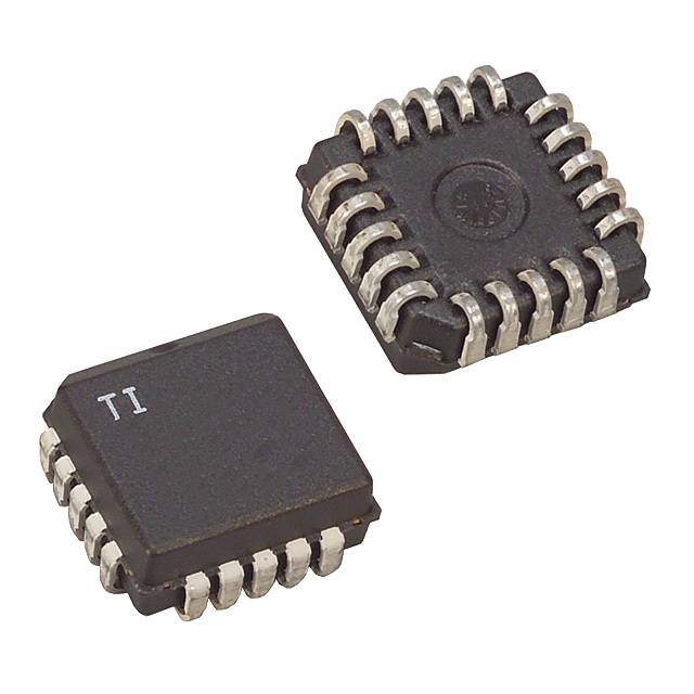
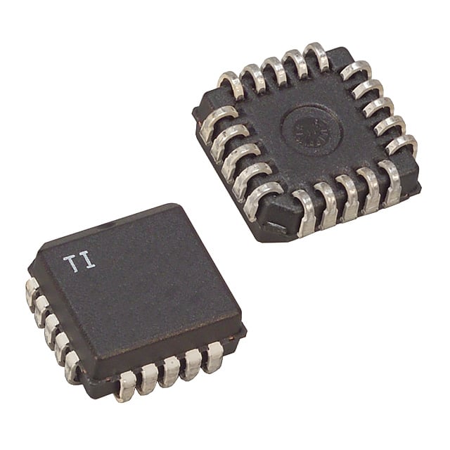
| 描述 | IC LEAD ACID BATT CHARGER 20PLCC电池管理 Lead-Acid Linear Charge Mngt IC |
| 产品分类 | |
| 品牌 | Texas Instruments |
| 产品手册 | |
| 产品图片 |
|
| rohs | 符合RoHS无铅 / 符合限制有害物质指令(RoHS)规范要求 |
| 产品系列 | 电源管理 IC,电池管理,Texas Instruments UC3906Q- |
| 数据手册 | |
| 产品型号 | UC3906Q |
| 产品目录页面 | |
| 产品种类 | 电池管理 |
| 供应商器件封装 | 20-PLCC(9x9) |
| 其它名称 | 296-12193-5 |
| 功能 | 充电管理 |
| 包装 | 管件 |
| 商标 | Texas Instruments |
| 安装类型 | 表面贴装 |
| 安装风格 | SMD/SMT |
| 封装 | Tube |
| 封装/外壳 | 20-LCC(J 形引线) |
| 封装/箱体 | PLCC-20 |
| 工作温度 | 0°C ~ 70°C |
| 工作电源电压 | 40 V |
| 工厂包装数量 | 46 |
| 最大工作温度 | + 70 C |
| 最小工作温度 | - 20 C |
| 标准包装 | 46 |
| 电压-电源 | 4.2 V ~ 40 V |
| 电池化学 | 铅酸 |
| 电池类型 | Lead Acid |
| 系列 | UC3906 |
| 输出电流 | 2 A |


- 商务部:美国ITC正式对集成电路等产品启动337调查
- 曝三星4nm工艺存在良率问题 高通将骁龙8 Gen1或转产台积电
- 太阳诱电将投资9.5亿元在常州建新厂生产MLCC 预计2023年完工
- 英特尔发布欧洲新工厂建设计划 深化IDM 2.0 战略
- 台积电先进制程称霸业界 有大客户加持明年业绩稳了
- 达到5530亿美元!SIA预计今年全球半导体销售额将创下新高
- 英特尔拟将自动驾驶子公司Mobileye上市 估值或超500亿美元
- 三星加码芯片和SET,合并消费电子和移动部门,撤换高东真等 CEO
- 三星电子宣布重大人事变动 还合并消费电子和移动部门
- 海关总署:前11个月进口集成电路产品价值2.52万亿元 增长14.8%


PDF Datasheet 数据手册内容提取
None
None
None
None
None
None
None
PACKAGE OPTION ADDENDUM www.ti.com 17-Mar-2017 PACKAGING INFORMATION Orderable Device Status Package Type Package Pins Package Eco Plan Lead/Ball Finish MSL Peak Temp Op Temp (°C) Device Marking Samples (1) Drawing Qty (2) (6) (3) (4/5) UC2906DW NRND SOIC DW 16 40 Green (RoHS CU NIPDAU Level-2-260C-1 YEAR -40 to 70 UC2906DW & no Sb/Br) UC2906DWG4 NRND SOIC DW 16 40 Green (RoHS CU NIPDAU Level-2-260C-1 YEAR -40 to 70 UC2906DW & no Sb/Br) UC2906DWTR NRND SOIC DW 16 2000 Green (RoHS CU NIPDAU Level-2-260C-1 YEAR -40 to 70 UC2906DW & no Sb/Br) UC2906N NRND PDIP N 16 25 Green (RoHS CU NIPDAU N / A for Pkg Type -40 to 70 UC2906N & no Sb/Br) UC2906NG4 NRND PDIP N 16 25 Green (RoHS CU NIPDAU N / A for Pkg Type -40 to 70 UC2906N & no Sb/Br) UC2906Q NRND PLCC FN 20 46 Green (RoHS CU SN Level-2-260C-1 YEAR -40 to 70 UC2906Q & no Sb/Br) UC3906DW NRND SOIC DW 16 40 Green (RoHS CU NIPDAU Level-2-260C-1 YEAR -20 to 70 UC3906DW & no Sb/Br) UC3906DWG4 NRND SOIC DW 16 40 Green (RoHS CU NIPDAU Level-2-260C-1 YEAR -20 to 70 UC3906DW & no Sb/Br) UC3906DWTR NRND SOIC DW 16 2000 Green (RoHS CU NIPDAU Level-2-260C-1 YEAR -20 to 70 UC3906DW & no Sb/Br) UC3906DWTRG4 NRND SOIC DW 16 2000 Green (RoHS CU NIPDAU Level-2-260C-1 YEAR -20 to 70 UC3906DW & no Sb/Br) UC3906N NRND PDIP N 16 25 Green (RoHS CU NIPDAU N / A for Pkg Type -20 to 70 UC3906N & no Sb/Br) UC3906NG4 NRND PDIP N 16 25 Green (RoHS CU NIPDAU N / A for Pkg Type -20 to 70 UC3906N & no Sb/Br) UC3906Q NRND PLCC FN 20 46 Green (RoHS CU SN Level-2-260C-1 YEAR -20 to 70 UC3906Q & no Sb/Br) UC3906QG3 NRND PLCC FN 20 46 Green (RoHS CU SN Level-2-260C-1 YEAR -20 to 70 UC3906Q & no Sb/Br) (1) The marketing status values are defined as follows: ACTIVE: Product device recommended for new designs. LIFEBUY: TI has announced that the device will be discontinued, and a lifetime-buy period is in effect. NRND: Not recommended for new designs. Device is in production to support existing customers, but TI does not recommend using this part in a new design. PREVIEW: Device has been announced but is not in production. Samples may or may not be available. OBSOLETE: TI has discontinued the production of the device. Addendum-Page 1
PACKAGE OPTION ADDENDUM www.ti.com 17-Mar-2017 (2) Eco Plan - The planned eco-friendly classification: Pb-Free (RoHS), Pb-Free (RoHS Exempt), or Green (RoHS & no Sb/Br) - please check http://www.ti.com/productcontent for the latest availability information and additional product content details. TBD: The Pb-Free/Green conversion plan has not been defined. Pb-Free (RoHS): TI's terms "Lead-Free" or "Pb-Free" mean semiconductor products that are compatible with the current RoHS requirements for all 6 substances, including the requirement that lead not exceed 0.1% by weight in homogeneous materials. Where designed to be soldered at high temperatures, TI Pb-Free products are suitable for use in specified lead-free processes. Pb-Free (RoHS Exempt): This component has a RoHS exemption for either 1) lead-based flip-chip solder bumps used between the die and package, or 2) lead-based die adhesive used between the die and leadframe. The component is otherwise considered Pb-Free (RoHS compatible) as defined above. Green (RoHS & no Sb/Br): TI defines "Green" to mean Pb-Free (RoHS compatible), and free of Bromine (Br) and Antimony (Sb) based flame retardants (Br or Sb do not exceed 0.1% by weight in homogeneous material) (3) MSL, Peak Temp. - The Moisture Sensitivity Level rating according to the JEDEC industry standard classifications, and peak solder temperature. (4) There may be additional marking, which relates to the logo, the lot trace code information, or the environmental category on the device. (5) Multiple Device Markings will be inside parentheses. Only one Device Marking contained in parentheses and separated by a "~" will appear on a device. If a line is indented then it is a continuation of the previous line and the two combined represent the entire Device Marking for that device. (6) Lead/Ball Finish - Orderable Devices may have multiple material finish options. Finish options are separated by a vertical ruled line. Lead/Ball Finish values may wrap to two lines if the finish value exceeds the maximum column width. Important Information and Disclaimer:The information provided on this page represents TI's knowledge and belief as of the date that it is provided. TI bases its knowledge and belief on information provided by third parties, and makes no representation or warranty as to the accuracy of such information. Efforts are underway to better integrate information from third parties. TI has taken and continues to take reasonable steps to provide representative and accurate information but may not have conducted destructive testing or chemical analysis on incoming materials and chemicals. TI and TI suppliers consider certain information to be proprietary, and thus CAS numbers and other limited information may not be available for release. In no event shall TI's liability arising out of such information exceed the total purchase price of the TI part(s) at issue in this document sold by TI to Customer on an annual basis. Addendum-Page 2
PACKAGE MATERIALS INFORMATION www.ti.com 30-Apr-2014 TAPE AND REEL INFORMATION *Alldimensionsarenominal Device Package Package Pins SPQ Reel Reel A0 B0 K0 P1 W Pin1 Type Drawing Diameter Width (mm) (mm) (mm) (mm) (mm) Quadrant (mm) W1(mm) UC2906DWTR SOIC DW 16 2000 330.0 16.4 10.75 10.7 2.7 12.0 16.0 Q1 UC3906DWTR SOIC DW 16 2000 330.0 16.4 10.75 10.7 2.7 12.0 16.0 Q1 PackMaterials-Page1
PACKAGE MATERIALS INFORMATION www.ti.com 30-Apr-2014 *Alldimensionsarenominal Device PackageType PackageDrawing Pins SPQ Length(mm) Width(mm) Height(mm) UC2906DWTR SOIC DW 16 2000 367.0 367.0 38.0 UC3906DWTR SOIC DW 16 2000 367.0 367.0 38.0 PackMaterials-Page2
None
4215152/B 04/2017 PACKAGE OUTLINE FN0020A PLCC - 4.57 mm max height SCALE 1.300 PLASTIC CHIP CARRIER .180 MAX B .350-.356 [4.57] [8.89-9.04] .020 MIN NOTE 3 [0.51] A (.008) 3 1 20 [0.2] 4 18 PIN 1 ID .350-.356 (OPTIONAL) .283-.339 [8.89-9.04] [7.19-8.61] NOTE 3 8 14 9 13 .090-.120 TYP [2.29-3.04] 20X .026-.032 [0.66-0.81] C SEATING PLANE 20X .013-.021 [0.33-0.53] .004 [0.1] C 16X .050 .007 [0.18] C A B [1.27] .385-.395 [9.78-10.03] TYP 4215152/B 04/2017 NOTES: 1. All linear dimensions are in inches. Any dimensions in brackets are in millimeters. Any dimensions in parenthesis are for reference only. Controlling dimensions are in inches. Dimensioning and tolerancing per ASME Y14.5M. 2. This drawing is subject to change without notice. 3. Dimension does not include mold protrusion. Maximum allowable mold protrusion .01 in [0.25 mm] per side. 4. Reference JEDEC registration MS-018. www.ti.com
4215152/B 04/2017 EXAMPLE BOARD LAYOUT FN0020A PLCC - 4.57 mm max height PLASTIC CHIP CARRIER SYMM (R.002 ) TYP 20X (.096 ) 3 1 20 [0.05] [2.45] 20X (.025 ) [0.64] 4 18 SYMM (.327) [8.3] 16X (.050 ) [1.27] 14 8 9 13 (.327) [8.3] LAND PATTERN EXAMPLE EXPOSED METAL SHOWN SCALE:6X .002 MIN .002 MAX EXPOSED METAL EXPOSED METAL [0.05] [0.05] ALL AROUND ALL AROUND METAL SOLDER MASK SOLDER MASK METAL UNDER OPENING OPENING SOLDER MASK NON SOLDER MASK SOLDER MASK DEFINED DEFINED (PREFERRED) SOLDER MASK DETAILS 4215152/B 04/2017 NOTES: (continued) 5. Publication IPC-7351 may have alternate designs. 6. Solder mask tolerances between and around signal pads can vary based on board fabrication site. www.ti.com
EXAMPLE STENCIL DESIGN FFNN00002200AA PPLLCCCC -- 44..5577 mmmm mmaaxx hheeiigghhtt PPLLAASSTTIICC CCHHIIPP CCAARRRRIIEERR SYMM (R.002 ) TYP 20X (.096 ) 3 1 20 [0.05] [2.45] 20X (.025 ) [0.64] 4 18 SYMM (.327) [8.3] 16X (.050 ) [1.27] 14 8 9 13 (.327) [8.3] SOLDER PASTE EXAMPLE BASED ON 0.125 mm THICK STENCIL SCALE:6X 4215152/B 04/2017 NOTES: (continued) 7. Laser cutting apertures with trapezoidal walls and rounded corners may offer better paste release. IPC-7525 may have alternate design recommendations. 8. Board assembly site may have different recommendations for stencil design. www.ti.com
GENERIC PACKAGE VIEW DW 16 SOIC - 2.65 mm max height SMALL OUTLINE INTEGRATED CIRCUIT Images above are just a representation of the package family, actual package may vary. Refer to the product data sheet for package details. 4040000-2/H
PACKAGE OUTLINE DW0016A SOIC - 2.65 mm max height SCALE 1.500 SOIC C 10.63 SEATING PLANE TYP 9.97 A PIN 1 ID 0.1 C AREA 14X 1.27 16 1 10.5 2X 10.1 8.89 NOTE 3 8 9 0.51 16X 0.31 7.6 B 7.4 0.25 C A B 2.65 MAX NOTE 4 0.33 TYP 0.10 SEE DETAIL A 0.25 GAGE PLANE 0.3 0 - 8 0.1 1.27 0.40 DETAIL A (1.4) TYPICAL 4220721/A 07/2016 NOTES: 1. All linear dimensions are in millimeters. Dimensions in parenthesis are for reference only. Dimensioning and tolerancing per ASME Y14.5M. 2. This drawing is subject to change without notice. 3. This dimension does not include mold flash, protrusions, or gate burrs. Mold flash, protrusions, or gate burrs shall not exceed 0.15 mm, per side. 4. This dimension does not include interlead flash. Interlead flash shall not exceed 0.25 mm, per side. 5. Reference JEDEC registration MS-013. www.ti.com
EXAMPLE BOARD LAYOUT DW0016A SOIC - 2.65 mm max height SOIC 16X (2) SEE SYMM DETAILS 1 16 16X (0.6) SYMM 14X (1.27) 8 9 R0.05 TYP (9.3) LAND PATTERN EXAMPLE SCALE:7X METAL SOLDER MASK SOLDER MASK METAL OPENING OPENING 0.07 MAX 0.07 MIN ALL AROUND ALL AROUND NON SOLDER MASK SOLDER MASK DEFINED DEFINED SOLDER MASK DETAILS 4220721/A 07/2016 NOTES: (continued) 6. Publication IPC-7351 may have alternate designs. 7. Solder mask tolerances between and around signal pads can vary based on board fabrication site. www.ti.com
EXAMPLE STENCIL DESIGN DW0016A SOIC - 2.65 mm max height SOIC 16X (2) SYMM 1 16 16X (0.6) SYMM 14X (1.27) 8 9 R0.05 TYP (9.3) SOLDER PASTE EXAMPLE BASED ON 0.125 mm THICK STENCIL SCALE:7X 4220721/A 07/2016 NOTES: (continued) 8. Laser cutting apertures with trapezoidal walls and rounded corners may offer better paste release. IPC-7525 may have alternate design recommendations. 9. Board assembly site may have different recommendations for stencil design. www.ti.com
None
IMPORTANTNOTICE TexasInstrumentsIncorporated(TI)reservestherighttomakecorrections,enhancements,improvementsandotherchangestoits semiconductorproductsandservicesperJESD46,latestissue,andtodiscontinueanyproductorserviceperJESD48,latestissue.Buyers shouldobtainthelatestrelevantinformationbeforeplacingordersandshouldverifythatsuchinformationiscurrentandcomplete. TI’spublishedtermsofsaleforsemiconductorproducts(http://www.ti.com/sc/docs/stdterms.htm)applytothesaleofpackagedintegrated circuitproductsthatTIhasqualifiedandreleasedtomarket.AdditionaltermsmayapplytotheuseorsaleofothertypesofTIproductsand services. ReproductionofsignificantportionsofTIinformationinTIdatasheetsispermissibleonlyifreproductioniswithoutalterationandis accompaniedbyallassociatedwarranties,conditions,limitations,andnotices.TIisnotresponsibleorliableforsuchreproduced documentation.Informationofthirdpartiesmaybesubjecttoadditionalrestrictions.ResaleofTIproductsorserviceswithstatements differentfromorbeyondtheparametersstatedbyTIforthatproductorservicevoidsallexpressandanyimpliedwarrantiesforthe associatedTIproductorserviceandisanunfairanddeceptivebusinesspractice.TIisnotresponsibleorliableforanysuchstatements. BuyersandotherswhoaredevelopingsystemsthatincorporateTIproducts(collectively,“Designers”)understandandagreethatDesigners remainresponsibleforusingtheirindependentanalysis,evaluationandjudgmentindesigningtheirapplicationsandthatDesignershave fullandexclusiveresponsibilitytoassurethesafetyofDesigners'applicationsandcomplianceoftheirapplications(andofallTIproducts usedinorforDesigners’applications)withallapplicableregulations,lawsandotherapplicablerequirements.Designerrepresentsthat,with respecttotheirapplications,Designerhasallthenecessaryexpertisetocreateandimplementsafeguardsthat(1)anticipatedangerous consequencesoffailures,(2)monitorfailuresandtheirconsequences,and(3)lessenthelikelihoodoffailuresthatmightcauseharmand takeappropriateactions.DesigneragreesthatpriortousingordistributinganyapplicationsthatincludeTIproducts,Designerwill thoroughlytestsuchapplicationsandthefunctionalityofsuchTIproductsasusedinsuchapplications. TI’sprovisionoftechnical,applicationorotherdesignadvice,qualitycharacterization,reliabilitydataorotherservicesorinformation, including,butnotlimitedto,referencedesignsandmaterialsrelatingtoevaluationmodules,(collectively,“TIResources”)areintendedto assistdesignerswhoaredevelopingapplicationsthatincorporateTIproducts;bydownloading,accessingorusingTIResourcesinany way,Designer(individuallyor,ifDesignerisactingonbehalfofacompany,Designer’scompany)agreestouseanyparticularTIResource solelyforthispurposeandsubjecttothetermsofthisNotice. TI’sprovisionofTIResourcesdoesnotexpandorotherwisealterTI’sapplicablepublishedwarrantiesorwarrantydisclaimersforTI products,andnoadditionalobligationsorliabilitiesarisefromTIprovidingsuchTIResources.TIreservestherighttomakecorrections, enhancements,improvementsandotherchangestoitsTIResources.TIhasnotconductedanytestingotherthanthatspecifically describedinthepublisheddocumentationforaparticularTIResource. Designerisauthorizedtouse,copyandmodifyanyindividualTIResourceonlyinconnectionwiththedevelopmentofapplicationsthat includetheTIproduct(s)identifiedinsuchTIResource.NOOTHERLICENSE,EXPRESSORIMPLIED,BYESTOPPELOROTHERWISE TOANYOTHERTIINTELLECTUALPROPERTYRIGHT,ANDNOLICENSETOANYTECHNOLOGYORINTELLECTUALPROPERTY RIGHTOFTIORANYTHIRDPARTYISGRANTEDHEREIN,includingbutnotlimitedtoanypatentright,copyright,maskworkright,or otherintellectualpropertyrightrelatingtoanycombination,machine,orprocessinwhichTIproductsorservicesareused.Information regardingorreferencingthird-partyproductsorservicesdoesnotconstitutealicensetousesuchproductsorservices,orawarrantyor endorsementthereof.UseofTIResourcesmayrequirealicensefromathirdpartyunderthepatentsorotherintellectualpropertyofthe thirdparty,oralicensefromTIunderthepatentsorotherintellectualpropertyofTI. TIRESOURCESAREPROVIDED“ASIS”ANDWITHALLFAULTS.TIDISCLAIMSALLOTHERWARRANTIESOR REPRESENTATIONS,EXPRESSORIMPLIED,REGARDINGRESOURCESORUSETHEREOF,INCLUDINGBUTNOTLIMITEDTO ACCURACYORCOMPLETENESS,TITLE,ANYEPIDEMICFAILUREWARRANTYANDANYIMPLIEDWARRANTIESOF MERCHANTABILITY,FITNESSFORAPARTICULARPURPOSE,ANDNON-INFRINGEMENTOFANYTHIRDPARTYINTELLECTUAL PROPERTYRIGHTS.TISHALLNOTBELIABLEFORANDSHALLNOTDEFENDORINDEMNIFYDESIGNERAGAINSTANYCLAIM, INCLUDINGBUTNOTLIMITEDTOANYINFRINGEMENTCLAIMTHATRELATESTOORISBASEDONANYCOMBINATIONOF PRODUCTSEVENIFDESCRIBEDINTIRESOURCESOROTHERWISE.INNOEVENTSHALLTIBELIABLEFORANYACTUAL, DIRECT,SPECIAL,COLLATERAL,INDIRECT,PUNITIVE,INCIDENTAL,CONSEQUENTIALOREXEMPLARYDAMAGESIN CONNECTIONWITHORARISINGOUTOFTIRESOURCESORUSETHEREOF,ANDREGARDLESSOFWHETHERTIHASBEEN ADVISEDOFTHEPOSSIBILITYOFSUCHDAMAGES. UnlessTIhasexplicitlydesignatedanindividualproductasmeetingtherequirementsofaparticularindustrystandard(e.g.,ISO/TS16949 andISO26262),TIisnotresponsibleforanyfailuretomeetsuchindustrystandardrequirements. WhereTIspecificallypromotesproductsasfacilitatingfunctionalsafetyorascompliantwithindustryfunctionalsafetystandards,such productsareintendedtohelpenablecustomerstodesignandcreatetheirownapplicationsthatmeetapplicablefunctionalsafetystandards andrequirements.Usingproductsinanapplicationdoesnotbyitselfestablishanysafetyfeaturesintheapplication.Designersmust ensurecompliancewithsafety-relatedrequirementsandstandardsapplicabletotheirapplications.DesignermaynotuseanyTIproductsin life-criticalmedicalequipmentunlessauthorizedofficersofthepartieshaveexecutedaspecialcontractspecificallygoverningsuchuse. Life-criticalmedicalequipmentismedicalequipmentwherefailureofsuchequipmentwouldcauseseriousbodilyinjuryordeath(e.g.,life support,pacemakers,defibrillators,heartpumps,neurostimulators,andimplantables).Suchequipmentincludes,withoutlimitation,all medicaldevicesidentifiedbytheU.S.FoodandDrugAdministrationasClassIIIdevicesandequivalentclassificationsoutsidetheU.S. TImayexpresslydesignatecertainproductsascompletingaparticularqualification(e.g.,Q100,MilitaryGrade,orEnhancedProduct). Designersagreethatithasthenecessaryexpertisetoselecttheproductwiththeappropriatequalificationdesignationfortheirapplications andthatproperproductselectionisatDesigners’ownrisk.Designersaresolelyresponsibleforcompliancewithalllegalandregulatory requirementsinconnectionwithsuchselection. DesignerwillfullyindemnifyTIanditsrepresentativesagainstanydamages,costs,losses,and/orliabilitiesarisingoutofDesigner’snon- compliancewiththetermsandprovisionsofthisNotice. MailingAddress:TexasInstruments,PostOfficeBox655303,Dallas,Texas75265 Copyright©2017,TexasInstrumentsIncorporated