ICGOO在线商城 > 集成电路(IC) > PMIC - 稳压器 - DC DC 切换控制器 > UC3845AN
 Datasheet下载
- 型号: UC3845AN
- 制造商: Texas Instruments
- 库位|库存: xxxx|xxxx
- 要求:
| 数量阶梯 | 香港交货 | 国内含税 |
| +xxxx | $xxxx | ¥xxxx |
查看当月历史价格
查看今年历史价格
UC3845AN产品简介:
ICGOO电子元器件商城为您提供UC3845AN由Texas Instruments设计生产,在icgoo商城现货销售,并且可以通过原厂、代理商等渠道进行代购。 UC3845AN价格参考¥4.45-¥10.21。Texas InstrumentsUC3845AN封装/规格:PMIC - 稳压器 - DC DC 切换控制器, 升压,降压,反激,正激转换器 稳压器 正,可提供隔离 输出 升压,降压,升压/降压 DC-DC 控制器 IC 8-PDIP。您可以下载UC3845AN参考资料、Datasheet数据手册功能说明书,资料中有UC3845AN 详细功能的应用电路图电压和使用方法及教程。
UC3845AN 是 Texas Instruments(德州仪器)推出的一款高性能电流模式 PWM 控制器,属于 PMIC(电源管理集成电路)中的 DC-DC 切换控制器类别。其主要应用场景包括:

1. 开关电源设计
   UC3845AN 广泛应用于开关电源(SMPS)的设计中,用于实现高效的直流到直流电压转换。它支持降压、升压和反激式拓扑结构,适用于多种功率转换场景。

2. 工业设备电源
   在工业自动化领域,UC3845AN 可用于为 PLC(可编程逻辑控制器)、传感器、执行器等设备提供稳定电源。其高精度的控制能力和宽输入电压范围使其适合复杂的工业环境。

3. 通信设备电源
   该芯片常用于通信基站、路由器和交换机的电源模块中,确保设备在不同负载条件下都能获得稳定的供电。

4. 消费电子设备
   UC3845AN 可用于笔记本适配器、显示器电源和其他消费类电子产品的电源设计,提供高效且可靠的电压调节功能。

5. LED 驱动电源
   在 LED 照明领域,UC3845AN 能够通过精确的电流控制实现高亮度 LED 的驱动,适用于路灯、广告屏和舞台照明等场景。

6. 电池充电器
   它可以用于设计高效的电池充电器,支持对锂离子电池、镍氢电池等多种电池类型的充电管理。

7. 太阳能逆变器辅助电源
   在太阳能发电系统中,UC3845AN 可用作逆变器的辅助电源控制器,提供稳定的内部供电。

UC3845AN 的关键特性包括高精度振荡器、温度补偿参考电压、强大的输出驱动器以及完善的保护机制(如过流保护和欠压锁定),这些特性使其成为许多需要高效、可靠电源解决方案的应用的理想选择。
| 参数 | 数值 |
| 产品目录 | 集成电路 (IC)半导体 |
| Cuk | 无 |
| 描述 | IC REG CTRLR PWM CM 8DIP开关控制器 Current Mode |
| 产品分类 | |
| 品牌 | Texas Instruments |
| 产品手册 | |
| 产品图片 |
|
| rohs | 符合RoHS无铅 / 符合限制有害物质指令(RoHS)规范要求 |
| 产品系列 | 电源管理 IC,开关控制器 ,Texas Instruments UC3845AN- |
| 数据手册 | |
| 产品型号 | UC3845AN |
| PWM类型 | 电流模式 |
| 上升时间 | 50 ns |
| 下降时间 | 50 ns |
| 产品目录页面 | |
| 产品种类 | 开关控制器 |
| 倍增器 | 无 |
| 其它名称 | 296-11297-5 |
| 分频器 | 无 |
| 包装 | 管件 |
| 升压 | 是 |
| 单位重量 | 528.600 mg |
| 占空比 | 50% |
| 占空比-最大 | 50 % |
| 反向 | 无 |
| 反激式 | 是 |
| 商标 | Texas Instruments |
| 安装风格 | Through Hole |
| 封装 | Tube |
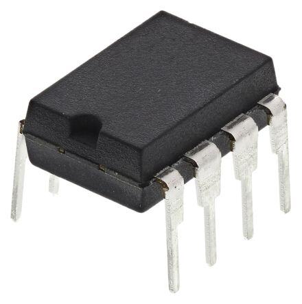
| 封装/外壳 | 8-DIP(0.300",7.62mm) |
| 封装/箱体 | PDIP-8 |
| 工作温度 | 0°C ~ 70°C |
| 工作电源电压 | 30 V |
| 工厂包装数量 | 50 |
| 开关频率 | 450 kHz |
| 拓扑结构 | Buck, Boost, Flyback, Forward |
| 最大工作温度 | + 70 C |
| 最小工作温度 | 0 C |
| 标准包装 | 50 |
| 电压-电源 | 7.6 V ~ 30 V |
| 类型 | Current Mode PWM Controllers |
| 系列 | UC3845A |
| 输出数 | 1 |
| 输出电压 | 4.90 V to 5.10 V |
| 输出电流 | 1000 mA |
| 输出端数量 | 1 Output |
| 降压 | 是 |
| 隔离式 | 无 |
| 频率-最大值 | 500kHz |


- 商务部:美国ITC正式对集成电路等产品启动337调查
- 曝三星4nm工艺存在良率问题 高通将骁龙8 Gen1或转产台积电
- 太阳诱电将投资9.5亿元在常州建新厂生产MLCC 预计2023年完工
- 英特尔发布欧洲新工厂建设计划 深化IDM 2.0 战略
- 台积电先进制程称霸业界 有大客户加持明年业绩稳了
- 达到5530亿美元!SIA预计今年全球半导体销售额将创下新高
- 英特尔拟将自动驾驶子公司Mobileye上市 估值或超500亿美元
- 三星加码芯片和SET,合并消费电子和移动部门,撤换高东真等 CEO
- 三星电子宣布重大人事变动 还合并消费电子和移动部门
- 海关总署:前11个月进口集成电路产品价值2.52万亿元 增长14.8%


PDF Datasheet 数据手册内容提取
Product Order Technical Tools & Support & Folder Now Documents Software Community UC1842A,UC1843A,UC1844A,UC1845A UC2842A,UC2843A,UC2844A,UC2845A UC3842A,UC3843A,UC3844A,UC3845A SLUS224F–SEPTEMBER1994–REVISEDOCTOBER2017 UCx84xA Current-Mode PWM Controller 1 Features 3 Description • OptimizedforOff-LineandDC-DCConverters TheUCx84xAfamilyofcontroldevicesisapin-for-pin 1 compatible improved version of the UCx84x family. • LowStart-UpCurrent(<0.5mA) Providing the necessary features to control current- • TrimmedOscillatorDischargeCurrent mode or switched-mode power supplies, this family of • AutomaticFeedforwardCompensation devices has many improved features: startup current is less than 0.5 mA, oscillator discharge is trimmed to • Pulse-by-PulseCurrentLimiting 8.3 mA, and during UVLO, the output stage can sink • EnhancedLoadResponseCharacteristics atleast10mAatlessthan1.2VforV over5V. CC • UndervoltageLockoutWithHysteresis DeviceInformation(1) • DoublePulseSuppression • High-CurrentTotemPoleOutput PARTNUMBER PACKAGE BODYSIZE(NOM) • Internally-TrimmedBandgapReference UC1842A,UC1843A, CDIP(8) 6.67mm×9.60mm UC1844A,UC1845A LCCC(20) 8.89mm×8.89mm • Upto500-kHzOperation UC2843A PLCC(20) 8.96mm×8.96mm • CreateaCustomDesignUsingtheUCx84xAWith PDIP(8) 6.35mm×9.81mm theWEBENCH®PowerDesigner UC2842A,UC2843A, UC2844A,UC2845A, SOIC(8) 3.91mm×4.90mm 2 Applications UC3842A,UC3843A, SOIC(14) 3.91mm×8.65mm UC3844A,UC3845A SOIC(16) 7.50mm×10.30mm • SwitchModePowerSupplies(SMPS) (1) For all available packages, see the orderable addendum at • DC-DCConverters theendofthedatasheet. • PowerModules • IndustrialPSU DeviceComparisonTable • BatteryOperatedPSU DEVICE UVLOON UVLOOFF MAXDUTY CYCLE UC1842A 16V 10V <100% UC1843A 8.4V 7.6V <100% UC1844A 16V 10V <50% UC1845A 8.4V 7.6V <50% SimplifiedApplicationDiagram VIN VCC OUTPUT VREF ISENSE UC2843A FB RT/CT GND COMP Copyright © 2017, Texas Instruments Incorporated 1 An IMPORTANT NOTICE at the end of this data sheet addresses availability, warranty, changes, use in safety-critical applications, intellectualpropertymattersandotherimportantdisclaimers.PRODUCTIONDATA.
UC1842A,UC1843A,UC1844A,UC1845A UC2842A,UC2843A,UC2844A,UC2845A UC3842A,UC3843A,UC3844A,UC3845A SLUS224F–SEPTEMBER1994–REVISEDOCTOBER2017 www.ti.com Table of Contents 1 Features.................................................................. 1 8 ApplicationandImplementation........................ 14 2 Applications........................................................... 1 8.1 ApplicationInformation............................................14 3 Description............................................................. 1 8.2 TypicalApplication..................................................14 4 RevisionHistory..................................................... 3 9 PowerSupplyRecommendations...................... 21 5 PinConfigurationandFunctions......................... 4 10 Layout................................................................... 22 6 Specifications......................................................... 6 10.1 LayoutGuidelines.................................................22 6.1 AbsoluteMaximumRatings......................................6 10.2 LayoutExample....................................................23 6.2 ESDRatings..............................................................6 11 DeviceandDocumentationSupport................. 24 6.3 RecommendedOperatingConditions.......................6 11.1 DeviceSupport......................................................24 6.4 ThermalInformation..................................................7 11.2 DocumentationSupport........................................24 6.5 ElectricalCharacteristics...........................................7 11.3 RelatedLinks........................................................25 6.6 TypicalCharacteristics..............................................9 11.4 ReceivingNotificationofDocumentationUpdates25 7 DetailedDescription............................................ 10 11.5 CommunityResources..........................................25 7.1 Overview.................................................................10 11.6 Trademarks...........................................................25 7.2 FunctionalBlockDiagram.......................................10 11.7 ElectrostaticDischargeCaution............................25 7.3 FeatureDescription.................................................10 11.8 Glossary................................................................25 7.4 DeviceFunctionalModes........................................13 12 Mechanical,Packaging,andOrderable Information........................................................... 26 2 SubmitDocumentationFeedback Copyright©1994–2017,TexasInstrumentsIncorporated ProductFolderLinks:UC1842AUC1843A UC1844A UC1845A UC2842A UC2843A UC2844A UC2845AUC3842A UC3843A UC3844A UC3845A
UC1842A,UC1843A,UC1844A,UC1845A UC2842A,UC2843A,UC2844A,UC2845A UC3842A,UC3843A,UC3844A,UC3845A www.ti.com SLUS224F–SEPTEMBER1994–REVISEDOCTOBER2017 4 Revision History NOTE:Pagenumbersforpreviousrevisionsmaydifferfrompagenumbersinthecurrentversion. ChangesfromRevisionE(October2017)toRevisionF Page • AddedWEBENCHlinksinthreeplaces,Features,ApplicationandImplementationandDeviceandDocumentation Support................................................................................................................................................................................... 1 • AddedcopyrightinformationtotheSimplifiedApplicationDiagram...................................................................................... 1 • Changedoperatingfree-airtemperatureoftheUC284xAchangedfrom125°Cto85°C. .................................................... 6 • Changedoperatingfree-airtemperatureoftheUC384xAchangedfrom-40°Cto0°C. ....................................................... 6 • Changedoperatingfree-airtemperatureoftheUC384xAchangedfrom85°Cto70°C. ...................................................... 6 • Changedthefrequency(f)calculationtothecorrectequation............................................................................................. 13 • ChangedtheC equationtothecorrectedequation. ...................................................................................................... 17 OUT • ChangedtheL equationtothecorrectedequation.......................................................................................................... 18 PM • AddedG (f)definitionandequation................................................................................................................................... 19 CO • Changedthef equationtothecorrectedequation......................................................................................................... 19 RHPz ChangesfromRevisionD(July2011)toRevisionE Page • AddedApplicationssection,DeviceInformationtable,PinConfigurationandFunctionssection,Specifications section,DetailedDescriptionsection,ApplicationandImplementationsection,PowerSupplyRecommendations section,Layoutsection,DeviceandDocumentationSupportsection,andMechanical,Packaging,andOrderable Informationsection................................................................................................................................................................. 1 • DeletedOrderingInformationTable;seePOAattheendofthedatasheet.......................................................................... 1 ChangesfromRevisionC(August2010)toRevisionD Page • ChangedAbsoluteMaximumratingstablewithmaximumnegativevoltageandGNDpinnotes......................................... 6 ChangesfromRevisionB(September2009)toRevisionC Page • CorrectedI voltage............................................................................................................................................................ 8 SINK Copyright©1994–2017,TexasInstrumentsIncorporated SubmitDocumentationFeedback 3 ProductFolderLinks:UC1842AUC1843A UC1844A UC1845A UC2842A UC2843A UC2844A UC2845AUC3842A UC3843A UC3844A UC3845A
UC1842A,UC1843A,UC1844A,UC1845A UC2842A,UC2843A,UC2844A,UC2845A UC3842A,UC3843A,UC3844A,UC3845A SLUS224F–SEPTEMBER1994–REVISEDOCTOBER2017 www.ti.com 5 Pin Configuration and Functions CDIP,PDIP,andSOICPackages SOICPackage 8-PinJG,P,andD 14-PinD TopView TopView COMP 1 8 VREF COMP 1 14 VREF FB 2 7 VCC NC 2 13 NC ISENSE 3 6 OUTPUT FB 3 12 VCC RT/CT 4 5 GND NC 4 11 VC ISENSE 5 10 OUTPUT Not to scale NC 6 9 GND RT/CT 7 8 PGND LCCCandPLCCPackages 20-PinFKandFN Not to scale TopView P F M E SOICPackage C O C R C N C N V N 16-PinDW TopView 3 2 1 0 9 2 1 NC 1 16 NC NC 4 18 VCC NC 2 15 VREF FB 5 17 VC COMP 3 14 VCC NC 6 16 NC FB 4 13 VCC ISENSE 7 15 OUTPUT ISENSE 5 12 OUTPUT NC 8 14 NC RT/CT 6 11 GND 0 1 2 3 9 1 1 1 1 NC 7 10 PGND NC 8 9 NC Not to scale C T C D D N C N N N T/ G G Not to scale R P 4 SubmitDocumentationFeedback Copyright©1994–2017,TexasInstrumentsIncorporated ProductFolderLinks:UC1842AUC1843A UC1844A UC1845A UC2842A UC2843A UC2844A UC2845AUC3842A UC3843A UC3844A UC3845A
UC1842A,UC1843A,UC1844A,UC1845A UC2842A,UC2843A,UC2844A,UC2845A UC3842A,UC3843A,UC3844A,UC3845A www.ti.com SLUS224F–SEPTEMBER1994–REVISEDOCTOBER2017 PinFunctions PIN NO. I/O DESCRIPTION NAME CDIP(8), LCCC(20), PDIP(8), SOIC(14) SOIC(16) PLCC(20) SOIC(8) Outputsthelowimpedance1-MHzinternalerroramplifierthatisalso theinputtothepeakcurrentlimitorPWMcomparator,withanopen- COMP 1 2 1 3 O loopgain(AVOL)of80dB.Thispiniscapableofsinkingamaximum of6mAandisnotinternallycurrentlimited. Inputtotheerroramplifierthatcanbeusedtocontrolthepower FB 2 5 3 4 I convertervoltage-feedbackloopforstability. GND 5 13 9 11 — Thisisthecontrollersignalground. Inputtothepeakcurrentlimit,PWMcomparatoroftheUCx84xA controllers.Whenusedinconjunctionwithacurrentsenseresistor, ISENSE 3 7 5 5 I theerroramplifieroutputvoltagecontrolsthepowersystemscycle- by-cyclepeakcurrentlimit.Themaximumpeakcurrentsensesignal isinternallyclampedto1V.SeeFunctionalBlockDiagram. Outputof1-Atotempolegatedriver.Thispincansinkandsource OUTPUT 6 15 10 12 O upto1Aofgatedrivercurrent.Agatedriverresistormustbeused tolimitthegatedrivercurrent. Powergroundandthegatedriverreturn.Fordevicesthathavethis pin,stargroundingtechniquescanbeusedtoredirectthegate PGND — 12 8 10 — drivercurrentawayfromthesignalgroundpin(GND).This techniquecanreducePWMcontrollerinstabilitiescausedbygate driverreturncurrent. Inputtotheinternaloscillatorthatisprogrammedwithanexternal timingresistor(RT)andtimingcapacitor(CT).SeeOscillatorfor informationonproperlyselectingthesetimingcomponents.TI RT/CT 4 10 7 6 I recommendsusingcapacitancevaluesfrom470pFto4.7nF.TI alsorecommendsthatthetimingresistorvalueschosenbefrom 5kΩto100kΩ. Biasinputtothegatedriver.ForPWMcontrollersthatdonothave thispin,thegatedriverisbiasedfromtheVCCpin.Thispinmust VC — 17 11 — I haveabiasingcapacitorthatisatleast10timesgreaterthanthe gatecapacitanceofthemainswitchingFETusedinthedesign. Biasinputtothegatedriver.Thispinmusthaveabiasingcapacitor VCC 7 18 12 13,14 I thatisatleast10timesgreaterthanthegatecapacitanceofthe mainswitchingFETusedinthedesign. ReferencevoltageoutputofthePWMcontroller.Thispinmust supplynomorethan10mAundernormaloperation.Thisoutputis short-circuitprotectedatroughly100mA.Thisreferenceisalsoused VREF 8 20 14 15 O forinternalcomparatorsandneedsahighfrequencybypass capacitorof1µF.TheVCCcapacitoralsomustbeatleast10times greaterthanthecapacitorontheVREFpin. 1,3,4,6,8, 1,2,7,8, NC — 9,11,14, 2,4,6,13 — Noconnection 9,16 16,19 Copyright©1994–2017,TexasInstrumentsIncorporated SubmitDocumentationFeedback 5 ProductFolderLinks:UC1842AUC1843A UC1844A UC1845A UC2842A UC2843A UC2844A UC2845AUC3842A UC3843A UC3844A UC3845A
UC1842A,UC1843A,UC1844A,UC1845A UC2842A,UC2843A,UC2844A,UC2845A UC3842A,UC3843A,UC3844A,UC3845A SLUS224F–SEPTEMBER1994–REVISEDOCTOBER2017 www.ti.com 6 Specifications 6.1 Absolute Maximum Ratings overoperatingfree-airtemperaturerange(unlessotherwisenoted)(1) MIN MAX UNIT Supplyvoltage(lowimpedancesource) VCCpin 30 V Outputcurrent,I ±1 A OUT Outputenergy(capacitiveload) 5 µJ Analoginputs –0.3 6.3 V Maximumnegativevoltage Allpins –0.3 V DifferentialvoltagebetweenVCandVCC VCpin –0.3 V Erroramplifieroutputsinkcurrent,I 10 mA COMP PowerdissipationatT ≤25°C 1 W A Leadtemperature(soldering,10s) 300 °C Junctiontemperature,T –55 150 °C J Storagetemperature,T –65 150 °C stg (1) StressesbeyondthoselistedunderAbsoluteMaximumRatingsmaycausepermanentdamagetothedevice.Thesearestressratings only,whichdonotimplyfunctionaloperationofthedeviceattheseoranyotherconditionsbeyondthoseindicatedunderRecommended OperatingConditions.Exposuretoabsolute-maximum-ratedconditionsforextendedperiodsmayaffectdevicereliability. 6.2 ESD Ratings VALUE UNIT Human-bodymodel(HBM),perANSI/ESDA/JEDECJS-001(1) ±2000 V Electrostaticdischarge V (ESD) Charged-devicemodel(CDM),perJEDECspecificationJESD22-C101(2) ±1500 (1) JEDECdocumentJEP155statesthat500-VHBMallowssafemanufacturingwithastandardESDcontrolprocess. (2) JEDECdocumentJEP157statesthat250-VCDMallowssafemanufacturingwithastandardESDcontrolprocess. 6.3 Recommended Operating Conditions overoperatingfree-airtemperaturerange(unlessotherwisenoted) MIN NOM MAX UNIT V Biassupplyvoltage VCCpin 11 V CC V ,V ,V Voltageonanalogpins FB,ISENSE,andRT/CTpins –0.1 5 V FB RC VFB V Gatedriveroutputvoltage –0.1 V V OUT CC I Supplybiascurrent 25 mA VCC I Outputcurrent VREFpin 10 mA VREF f Oscillatorfrequency 500 kHz OSC UC184xA –55 125 T Operatingfree-airtemperature UC284xA –40 85 °C A UC384xA 0 70 6 SubmitDocumentationFeedback Copyright©1994–2017,TexasInstrumentsIncorporated ProductFolderLinks:UC1842AUC1843A UC1844A UC1845A UC2842A UC2843A UC2844A UC2845AUC3842A UC3843A UC3844A UC3845A
UC1842A,UC1843A,UC1844A,UC1845A UC2842A,UC2843A,UC2844A,UC2845A UC3842A,UC3843A,UC3844A,UC3845A www.ti.com SLUS224F–SEPTEMBER1994–REVISEDOCTOBER2017 6.4 Thermal Information UC184xA UC2843A UC284xA,UC384xA THERMALMETRIC(1) JG(CDIP) FK(LCCC) FN(PLCC) P(PDIP) D(SOIC) D(SOIC) DW(SOIC) UNIT 8PINS 20PINS 20PINS 8PINS 8PINS 14PINS 16PINS Junction-to-ambientthermal R — — 56.7 53.4 104.3 77.9 73.6 °C/W θJA resistance Junction-to-case(top) R 64 36.2 34.6 46.4 46.8 35.8 35 °C/W θJC(top) thermalresistance Junction-to-boardthermal R 92.5 35.4 21.8 30.7 45.3 32.5 38.4 °C/W θJB resistance Junction-to-top ψ — — 10.4 16.8 6 6.6 9.7 °C/W JT characterizationparameter Junction-to-board ψ — — 21.5 30.6 44.6 32.2 37.8 °C/W JB characterizationparameter Junction-to-case(bottom) R 15.1 4.1 — — — — — °C/W θJC(bot) thermalresistance (1) Formoreinformationabouttraditionalandnewthermalmetrics,seetheSemiconductorandICPackageThermalMetricsapplication report. 6.5 Electrical Characteristics Unlessotherwisestated,thesespecificationsapplyforT =–55°Cto125°C(UC184xA),T =–40°Cto125°C(UC284xAQ), A A T =–40°Cto85°C(UC284xA),T =0°Cto70°C(UC384xA);T =T;V =15V(1);R =10kΩ;C =3.3nF. A A A J CC T T PARAMETER TESTCONDITIONS MIN TYP MAX UNIT REFERENCE UC184xA,UC284xA 4.95 5 5.05 Outputvoltage T =25°C,I =1mA V J O UC384xA 4.9 5 5.1 Lineregulation 12≤V ≤25V 6 20 mV IN Loadregulation 1≤I ≤20mA 6 25 mV O Temperaturestability See (2)(3) 0.2 0.4 mV/°C UC184xA,UC284xA 4.9 5.1 Totaloutputvariation Line,Load,Temperature V UC384xA 4.82 5.18 Outputnoisevoltage 10Hz≤f≤10kHz;T =25°C(2) 50 µV J Long-termstability T =125°C,1000hrs(2) 5 25 mV A Outputshortcircuit –30 –100 –180 mA OSCILLATOR Initialaccuracy T =25°C(4) 47 52 57 kHz J Voltagestability 12≤V ≤25V 0.2% 1% CC Temperaturestability T ≤T ≤T (2) 5% MIN A MAX Amplitude V peaktopeak(2) 1.7 V RT/CT T =25°C,V =2V(5) 7.8 8.3 8.8 J RT/CT Dischargecurrent UC184xA,UC284xA 7.5 8.8 mA V =2V(5) RT/CT UC384xA 7.6 8.8 (1) AdjustV abovethestartthresholdbeforesettingat15V. CC (2) Ensuredbydesign,butnot100%productiontested. (3) Temperaturestability,sometimesreferredtoasaveragetemperaturecoefficient,isdescribedby:Temperaturestability=(V – REF(max) V )/(T –T ).V andV arethemaximumandminimumreferencevoltagemeasuredovertheappropriate REF(min) J(max) J(min) REF(max) REF(min) temperaturerange.Notethattheextremesinvoltagedonotnecessarilyoccurattheextremesintemperature. (4) OutputfrequencyequalsoscillatorfrequencyfortheUC1842AandUC1843A.Outputfrequencyisonehalfoscillatorfrequencyforthe UC1844AandUC1845A. (5) ThisparameterismeasuredwithR =10kΩtoV .Thiscontributesapproximately300µAofcurrenttothemeasurement.Thetotal T REF currentflowingintotheRT/CTpinisapproximately300µAhigherthanthemeasuredvalue. Copyright©1994–2017,TexasInstrumentsIncorporated SubmitDocumentationFeedback 7 ProductFolderLinks:UC1842AUC1843A UC1844A UC1845A UC2842A UC2843A UC2844A UC2845AUC3842A UC3843A UC3844A UC3845A
UC1842A,UC1843A,UC1844A,UC1845A UC2842A,UC2843A,UC2844A,UC2845A UC3842A,UC3843A,UC3844A,UC3845A SLUS224F–SEPTEMBER1994–REVISEDOCTOBER2017 www.ti.com Electrical Characteristics (continued) Unlessotherwisestated,thesespecificationsapplyforT =–55°Cto125°C(UC184xA),T =–40°Cto125°C(UC284xAQ), A A T =–40°Cto85°C(UC284xA),T =0°Cto70°C(UC384xA);T =T;V =15V(1);R =10kΩ;C =3.3nF. A A A J CC T T PARAMETER TESTCONDITIONS MIN TYP MAX UNIT ERRORAMPLIFIER UC184xA,UC284xA 2.45 2.5 2.55 Inputvoltage V =2.5V V COMP UC384xA 2.42 2.5 2.58 –0.3 –1 Inputbiascurrent µA –0.3 –2 A Open-loopgain 2≤V ≤4V 65 90 dB VOL O Unitygainbandwidth T =25°C(2) 0.7 1 MHz J CMRR Commonmoderejectionratio 12≤V ≤25V 60 70 dB CC Outputsinkcurrent V =2.7V,V =1.1V 2 6 mA FB COMP Outputsourcecurrent V =2.3V,V =5V –0.5 –0.8 mA FB COMP V high V =2.3V,R =15kΩtoground 5 6 V OUT FB L V low V =2.7V,R =15kΩtoVREF 0.7 1.1 V OUT FB L CURRENTSENSE Gain See (6)(7) 2.85 3 3.15 V/V Maximuminputsignal V =5V(6) 0.9 1 1.1 V COMP PSRR Powersupplyrejectionratio 12≤V 25V(6) 70 dB CC Inputbiascurrent –2 –10 µA Delaytooutput V =0to2V(2) 150 300 ns ISENSE OUTPUT I =20mA 0.1 0.4 SINK Outputlowlevel V I =200mA 15 2.2 SINK I =20mA 13 13.5 SOURCE Outputhighlevel V I =200mA 12 13.5 SOURCE Risetime T =25°C,C =1nF(2) 50 150 ns J L Falltime T =25°C,C =1nF(2) 50 150 ns J L UVLOsaturation V =5V,I =10mA 0.7 1.2 V CC SINK UNDERVOLTAGELOCKOUT UC1842A,UC1844A,UC2842A,andUC2844A 15 16 17 Startthreshold UC3842AandUC3844A 14.5 16 17.5 V UCx843AandUCx845A 7.8 8.4 9 UC1842A,UC1844A,UC2842A,andUC2844A 9 10 11 Minimumoperationvoltageafter UC3842AandUC3844A 8.5 10 11.5 V turnon UCx843AandUCx845A 7 7.6 8.2 PWM UCx842A,UCx843A 94% 96% 100% Maximumdutycycle UCx844A,UCx845A 47% 48% 50% Minimumdutycycle 0% TOTALSTANDBYCURRENT Start-upcurrent 0.3 0.5 mA Operatingsupplycurrent V =V =0V 11 17 mA FB ISENSE V Zenervoltage I =25mA 30 34 V CC CC (6) ParametermeasuredattrippointoflatchwithV =0. FB (7) Gaindefinedas:A=ΔV /ΔV ;0≤V ≤0.8V. COMP ISENSE ISENSE 8 SubmitDocumentationFeedback Copyright©1994–2017,TexasInstrumentsIncorporated ProductFolderLinks:UC1842AUC1843A UC1844A UC1845A UC2842A UC2843A UC2844A UC2845AUC3842A UC3843A UC3844A UC3845A
UC1842A,UC1843A,UC1844A,UC1845A UC2842A,UC2843A,UC2844A,UC2845A UC3842A,UC3843A,UC3844A,UC3845A www.ti.com SLUS224F–SEPTEMBER1994–REVISEDOCTOBER2017 6.6 Typical Characteristics Figure1.OutputSaturationCharacteristics Figure2.ErrorAmplifierOpen-LoopFrequencyResponse Copyright©1994–2017,TexasInstrumentsIncorporated SubmitDocumentationFeedback 9 ProductFolderLinks:UC1842AUC1843A UC1844A UC1845A UC2842A UC2843A UC2844A UC2845AUC3842A UC3843A UC3844A UC3845A
UC1842A,UC1843A,UC1844A,UC1845A UC2842A,UC2843A,UC2844A,UC2845A UC3842A,UC3843A,UC3844A,UC3845A SLUS224F–SEPTEMBER1994–REVISEDOCTOBER2017 www.ti.com 7 Detailed Description 7.1 Overview The UCx84xA family of fixed-frequency pulse-width-modulator (PWM) controllers are designed to operate at switching frequencies of 500 kHz. These controllers are designed for peak current mode (PCM) and can be used in isolated and non-isolated power supply designs. These controllers can drive FETs directly from the output, which is capable of sourcing and sinking up to 1 A of gate driver current. These devices also have a built-in low- impedance amplifier that can be used in non-isolated designs to control the power supply output voltage and feedbackloop. 7.2 Functional Block Diagram VCC UVLO 34 V 5 V VREF S/R REF 5 V GND 2.5 V Internal Bias VREF Good VC Logic RT/CT OSC OUTPUT T S + 2R PWM Error Latch GND Amp R FB – R 1 V Current Sense COMP Comparator ISENSE Copyright © 2016,Texas Instruments Incorporated 7.3 Feature Description 7.3.1 Pulse-by-PulseCurrentLimiting Pulse-by-pulse limiting is inherent in the current mode control scheme. An upper limit on the peak current can be established by simply clamping the error voltage. Accurate current limiting allows optimization of magnetic and powersemiconductorelementswhileensuringreliablesupplyoperation. 7.3.2 CurrentSenseCircuit Peakcurrent(I )isdeterminedbyEquation1: S 1V I ´ S(max) R S (1) AsmallRCfiltermayberequiredtosuppressswitchtransients. 10 SubmitDocumentationFeedback Copyright©1994–2017,TexasInstrumentsIncorporated ProductFolderLinks:UC1842AUC1843A UC1844A UC1845A UC2842A UC2843A UC2844A UC2845AUC3842A UC3843A UC3844A UC3845A
UC1842A,UC1843A,UC1844A,UC1845A UC2842A,UC2843A,UC2844A,UC2845A UC3842A,UC3843A,UC3844A,UC3845A www.ti.com SLUS224F–SEPTEMBER1994–REVISEDOCTOBER2017 Feature Description (continued) Figure3. CurrentSenseCircuitDiagram 7.3.3 ErrorAmplifierConfiguration Theerroramplifiercansourceupto0.8mA,andsinkupto6mA. Figure4. ErrorAmplifierConfigurationDiagram 7.3.4 UndervoltageLockout The UCx84xA devices feature undervoltage lockout protection circuits for controlled operation during power-up and power-down sequences. Undervoltage lockout thresholds for the UCx842A, UCx843A, UCx844A, and UCx845A devices are optimized for two groups of applications: off-line power supplies and DC-DC converters. With a wider VCC to VCC range, the UCx842A and UCx844A devices are ideally suited to off-line AC input ON OFF applications. The UCx843A and UCx845A controllers have a much narrower VCC to VCC hysteresis and ON OFF maybeusedinDCtoDCapplicationswheretheinputisconsideredregulated. During UVLO the IC draws typically 0.3 mA of supply current. This VCC current is considerable less than the UCx84x family and results in lower power drawn from the line. The reduced start-up current is of particular concern in off-line supplies where the IC is powered-up from the high-voltage DC rail, then bootstrapped to an auxiliary winding on the main transformer. Power is then dissipated in the start-up resistor which is sized by the IC’s start-up current. Lowering this by 50% in the UCx84xA version family, as compared to the UCx84x family, reduces the resistors power loss by the same percentage. Once crossing the turnon threshold the IC supply current increases typically to about 11 mA, During undervoltage lockout, the UCx84xA series of devices prevent thepowerMOSFETfromparasiticallyturningonduetothe Millereffectatpower-up.Thisimproveddesigntothe lower totem-pole transistor’s operation during undervoltage lockout allows the IC to sink higher currents, up to 10 mA,atsaturationvoltagesaslowas0.7V,comparedtotheUCx84xdeviceswhichwouldonlysinkupto0.2mA underthesameconditions. Copyright©1994–2017,TexasInstrumentsIncorporated SubmitDocumentationFeedback 11 ProductFolderLinks:UC1842AUC1843A UC1844A UC1845A UC2842A UC2843A UC2844A UC2845AUC3842A UC3843A UC3844A UC3845A
UC1842A,UC1843A,UC1844A,UC1845A UC2842A,UC2843A,UC2844A,UC2845A UC3842A,UC3843A,UC3844A,UC3845A SLUS224F–SEPTEMBER1994–REVISEDOCTOBER2017 www.ti.com Feature Description (continued) DuringUVLO, the Output is low. Figure5. UndervoltageLockout 7.3.5 Oscillator 100 Hz) 1 M %) 80 uency ( Cycle ( Freq 100 k Duty 60 or m Oscillat C Maximu 10 k T 40 470 pF 1 nF 2.2 nF 4.7nF 20 300 1 k 3 k 10 k 30 k 100 k 300 1 k 3 k 10 k 30 k 100 k RT(Ω) RT(Ω) Figure6.OscillatorFrequencyvsTimingResistance Figure7.MaximumDutyCyclevsTimingResistance 12 SubmitDocumentationFeedback Copyright©1994–2017,TexasInstrumentsIncorporated ProductFolderLinks:UC1842AUC1843A UC1844A UC1845A UC2842A UC2843A UC2844A UC2845AUC3842A UC3843A UC3844A UC3845A
UC1842A,UC1843A,UC1844A,UC1845A UC2842A,UC2843A,UC2844A,UC2845A UC3842A,UC3843A,UC3844A,UC3845A www.ti.com SLUS224F–SEPTEMBER1994–REVISEDOCTOBER2017 Feature Description (continued) 8 R T 4 C T 5 (cid:218).(cid:224)(cid:219) (cid:244)(cid:23)(cid:26) (cid:0) >(cid:222) (cid:19) (cid:14) N (cid:2) (cid:0) (cid:215)æ (cid:2) (cid:2) Figure8.OscillatorSection Figure9.SlopeCompensation Precision operation at high frequencies with an accurate maximum duty cycle, see Figure 7, can now be obtained with the UCx84xA family of devices due to its trimmed oscillator discharge current. This nullifies the effects of production variations in the initial discharge current or dead time. Previous versions of the UCx84x devices had greater than a 2:1 oscillator discharge current range and resulted in less reliable maximum duty cycleprogramming. A fraction of the oscillator ramp can be resistively summed with the current sense signal, to provide slope compensation for converters requiring duty cycles over 50%. Capacitor C forms a filter with R2 to suppress the leading-edgeswitchspikes. 7.4 Device Functional Modes 7.4.1 NormalOperation The IC can be used in peak current mode (PCM) control or voltage mode (VM) control. When the converter is operatinginPCM,thevoltageamplifieroutputwillregulatetheconverter'speakcurrentanddutycycle.Whenthe IC is used in VM control, the voltage amplifier output will regulate the power converter's duty cycle. The regulation of the system's peak current and duty cycle can be achieved with the use of the integrated error amplifierandexternalfeedbackcircuitry. 7.4.2 UndervoltageLockout(UVLO)Start-Up During system start-up, VCC voltage starts to rise from 0. Before the VCC voltage reaches its corresponding start threshold, the IC is operating in UVLO mode. After the UVLO turn start-up threshold is met the device will becomeactiveandthereferencewillcomeupto5V. 7.4.3 UVLOTurnoffMode If the bias voltage to VCC drops below the UVLO minimum operating voltage, PWM switching stops and the reference will become inactive, returning to 0 V. The device can be restarted by applying a voltage greater than theUVLOstartthresholdtotheVCCpin. Copyright©1994–2017,TexasInstrumentsIncorporated SubmitDocumentationFeedback 13 ProductFolderLinks:UC1842AUC1843A UC1844A UC1845A UC2842A UC2843A UC2844A UC2845AUC3842A UC3843A UC3844A UC3845A
UC1842A,UC1843A,UC1844A,UC1845A UC2842A,UC2843A,UC2844A,UC2845A UC3842A,UC3843A,UC3844A,UC3845A SLUS224F–SEPTEMBER1994–REVISEDOCTOBER2017 www.ti.com 8 Application and Implementation NOTE Information in the following applications sections is not part of the TI component specification, and TI does not warrant its accuracy or completeness. TI’s customers are responsible for determining suitability of components for their purposes. Customers should validateandtesttheirdesignimplementationtoconfirmsystemfunctionality. 8.1 Application Information The UCx84xA controllers are peak-current mode pulse-width modulators. These controllers have an onboard amplifier and can be used in isolated or nonisolated power supply designs. There is an onboard totem-pole gate driver capable of delivering 1 A of peak current. This is a high-speed PWM capable of operating at switching frequenciesupto500kHz. 8.2 Typical Application A typical application for the UC3842A in an off-line flyback converter is shown in Figure 10. The UC3842A uses an inner current control loop that contains a small current sense resistor which senses the primary inductor current ramp. This current sense resistor transforms the inductor current waveform to a voltage signal that is input directly into the primary side PWM comparator. This inner loop determines the response to input voltage changes. An outer voltage control loop involves comparing a portion of the output voltage to a reference voltage at the input of an error amplifier. When used in an off-line isolated application, the voltage feedback of the isolated output is accomplished using a secondary-side error amplifier and adjustable voltage reference, such as the TL431. The error signal crosses the primary to secondary isolation boundary using an opto-isolator whose collector is connected to the VREF pin and the emitter is connected to FB. The outer voltage control loop determinestheresponsetoloadchanges. 14 SubmitDocumentationFeedback Copyright©1994–2017,TexasInstrumentsIncorporated ProductFolderLinks:UC1842AUC1843A UC1844A UC1845A UC2842A UC2843A UC2844A UC2845AUC3842A UC3843A UC3844A UC3845A
UC1842A,UC1843A,UC1844A,UC1845A UC2842A,UC2843A,UC2844A,UC2845A UC3842A,UC3843A,UC3844A,UC3845A www.ti.com SLUS224F–SEPTEMBER1994–REVISEDOCTOBER2017 Typical Application (continued) DCL FA 5A ~ DA CCL 10 nF RCL 50 kΩ DC VIN= 85 V to 265 VAC – + VOUT+ ~ NP CIN CVCC2 120 µF RH 300 kΩ VOUT– DB RD QA NA 22Ω VO RG 10Ω RE 1 kΩ RAC RCS VC UC3U8142A RF VO’ 1 COMP VREF 8 1 kΩ RT CA 1 nF RA 10 kΩ 2 FB VCC 7 DC 10 V RJ 1 kΩ CVCC1 CVREF 3 ISENSE OUTPUT 6 1 µF 1 µF VA 4 RT/CT GND 5 RS2 2.05 kΩ U2 RS1 CT CF 270 pF RP CP RI 200 kΩ VB RB RZ CZ CS1 10 nF 4.99 kΩ U3 TL431 RC 1 kΩ RK Copyright © 2016,Texas Instruments Incorporated Figure10. TypicalFlybackApplicationCircuit Copyright©1994–2017,TexasInstrumentsIncorporated SubmitDocumentationFeedback 15 ProductFolderLinks:UC1842AUC1843A UC1844A UC1845A UC2842A UC2843A UC2844A UC2845AUC3842A UC3843A UC3844A UC3845A
UC1842A,UC1843A,UC1844A,UC1845A UC2842A,UC2843A,UC2844A,UC2845A UC3842A,UC3843A,UC3844A,UC3845A SLUS224F–SEPTEMBER1994–REVISEDOCTOBER2017 www.ti.com Typical Application (continued) 8.2.1 DesignRequirements Forthisdesignexample,usetheparameterslistedinTable1astheinputparameters. Table1.DesignParameters PARAMETER MIN TYP MAX UNIT INPUTCHARACTERISTICS V Inputvoltage(RMS) 85 265 V IN f Linefrequency 47 63 Hz LINE OUTPUTCHARACTERISTICS V Outputvoltage 11.75 12 12.25 V OUT Outputripplevoltage 50 mV PP I Outputcurrent 4 4.33 A OUT Loadstep 11.75 12.25 V SYSTEMSCHARACTERISTICS η Maximumloadefficiency 86% 8.2.2 DetailedDesignProcedure 8.2.2.1 CustomDesignWithWEBENCH® Tools ClickheretocreateacustomdesignusingtheUCx84xAdevicewiththeWEBENCH® PowerDesigner. 1. Startbyenteringtheinputvoltage(V ),outputvoltage(V ),andoutputcurrent(I )requirements. IN OUT OUT 2. Optimizethedesignforkeyparameterssuchasefficiency,footprint,andcostusingtheoptimizerdial. 3. ComparethegenerateddesignwithotherpossiblesolutionsfromTexasInstruments. The WEBENCH Power Designer provides a customized schematic along with a list of materials with real-time pricingandcomponentavailability. Inmostcases,theseactionsareavailable: • Runelectricalsimulationstoseeimportantwaveformsandcircuitperformance • Runthermalsimulationstounderstandboardthermalperformance • ExportcustomizedschematicandlayoutintopopularCADformats • PrintPDFreportsforthedesign,andsharethedesignwithcolleagues GetmoreinformationaboutWEBENCHtoolsatwww.ti.com/WEBENCH. 8.2.2.2 UC2842ADesignProcedure This application design procedure shows how to setup and use the UC2842A peak current mode controller in an offlineflybackconverter,withuniversalinputtoa12-V,48-Wregulatedoutput. Setting up and designing with the UC2842A peak current mode controller in a continuous mode flyback application requires knowing some things about the power stage. First, calculate the required input bulk capacitance (C ) based on output power level (P ), efficiency (ƞ), minimum input voltage (V ), line IN OUT IN(min) frequency(f )andminimumbulkvoltage.ForthisdesignexampleletV =95V. LINE BULK(min) 2´POUT ´éê0.25+ 1´arcsin´æç VBULK(min) ö÷ùú h ë p è 2´VIN(min)øû V = INripple (2´V2 -V2 )´f IN(min) BULK(min) LINE (2) 2´POUT ´éê0.25+ 1´arcsin´æç VBULK(min) ö÷ùú h ë p è 2´VIN(min)øû C = »180µF IN (2´V2 -V2 )´f IN(min) BULK(min) LINE (3) 16 SubmitDocumentationFeedback Copyright©1994–2017,TexasInstrumentsIncorporated ProductFolderLinks:UC1842AUC1843A UC1844A UC1845A UC2842A UC2843A UC2844A UC2845AUC3842A UC3843A UC3844A UC3845A
UC1842A,UC1843A,UC1844A,UC1845A UC2842A,UC2843A,UC2844A,UC2845A UC3842A,UC3843A,UC3844A,UC3845A www.ti.com SLUS224F–SEPTEMBER1994–REVISEDOCTOBER2017 The output capacitor (C ) is sized so the output voltage does not droop more than 10% during a large-signal OUT transient response. The voltage-loop crossover frequency (f ) is estimated to be 2.5 kHz at this point in the C design. I OUT f C R C N1.33mF OUT V (cid:215)10% OUT (4) TheC selectedforthedesignisa2200-µFcapacitor,withanequivalentseriesresistance(ESR)of45mΩ. OUT Next calculate the maximum primary to secondary turns ratio (N ) of the transformer, based on the minimum PS inputvoltageandoutputvoltage. N £ VIN(min)´ 2 = 85 V´ 2 »10 PS V 12V OUT (5) Copyright©1994–2017,TexasInstrumentsIncorporated SubmitDocumentationFeedback 17 ProductFolderLinks:UC1842AUC1843A UC1844A UC1845A UC2842A UC2843A UC2844A UC2845AUC3842A UC3843A UC3844A UC3845A
UC1842A,UC1843A,UC1844A,UC1845A UC2842A,UC2843A,UC2844A,UC2845A UC3842A,UC3843A,UC3844A,UC3845A SLUS224F–SEPTEMBER1994–REVISEDOCTOBER2017 www.ti.com Nextcalculatetheauxiliarytosecondaryturnsratio(N )ofthetransformer,basedontheoutputvoltageandthe AS biasvoltageoftheUC2842A. V 12V N £ VCC = =1 AS V 12V OUT (6) Once the transformer turns ratios have been determined, the minimum primary magnetizing inductance (L ) of PM the transformer can be calculated based on minimum bulk voltage, Duty Cycle (D), reflected output current and efficiency.ThetransformerusedinthisdesignhasanL of1.7mH,N =10,andaN =1,f =100kHz PM PS AS sw N ´V D= PS OUT »0.56 V +N ´V BULK(min) PS OUT (7) V (cid:215)D L R BULK:min; =1.632mHN1.7mH PM 70%(cid:215)I (cid:215)f OUT sw D(cid:215)N PS (8) After the transformer has been selected, the primary peak current (I ) of the transformer can be calculated LpPK based on the primary magnetizing inductance ripple (I ) and the reflected output current across the LPM transformer. V ´D I = BULK(min) »0.31A LPM f ´L SW M (9) I I I = OUT + LM »1.1A LpPK N ´(1-D) 2 PS (10) Oncetheprimarypeakcurrenthasbeencalculatedthecurrentsenseresistor(R )canbeselected. CS 1V R = =0.725W»0.75W CS I ´1.3 LpPK (11) Resistors R and R are used to set the slope compensation of the design. Capacitor C is a DC blocking S1 S2 S1 capacitor, and pull-up resistor R is used to provide some offset to the current sense signal for noise immunity. P R andR werepreselectedtoaddaDCoffsetof50mVtothecurrentsensesignal. P S2 R is selected to set the slope compensation to one-half of the ripple current down slope of the flyback inductor. S1 This can be accomplished by calculating the secondary magnetizing inductance (L ) and using the following SM calculationforR .The1.7VintheR equationisthepeak-to-peakripplevoltageamplitudeoftheoscillator. S1 S1 1.7 V´R ´f ´(2´L ´N ) R = S2 SW SM PS -R =27.72kW»27.4kW S1 V ´(1-D)´R S2 OUT CS where R =2.05kW • S2 (12) Resistors R and R are selected to the output reference and can be calculated by preselecting a value for R I K K and knowing the TL431 reference voltage (V ). After choosing 2.49 kΩ for R , R is calculated and a TL431REF K I standardresistorvalueof9.53kΩ ischosenforthisresistor. R ´(V -V ) 2.49kW´(12V-2.5V) R = K OUT TL431REF = =9.462kW»9.53kW I V 2.5V TL431REF (13) This design using the UC2842A controller has an interesting control loop with many components. G (f) is the OPTO approximate transfer function across the opto isolator in the design. The pole frequency of the opto isolator is represented by f . The opto isolator used in this design has a current transfer ratio of 1 and pole frequency of P roughly 5 kHz. See Figure 10 for component placement and node voltages. The voltage loop (f ) must cross- C overlessthantheoptoisolatorpoleforsimplifiedcompensation. s(f)=2´p´1i´f (14) f =5kHz P (15) 18 SubmitDocumentationFeedback Copyright©1994–2017,TexasInstrumentsIncorporated ProductFolderLinks:UC1842AUC1843A UC1844A UC1845A UC2842A UC2843A UC2844A UC2845AUC3842A UC3843A UC3844A UC3845A
UC1842A,UC1843A,UC1844A,UC1845A UC2842A,UC2843A,UC2844A,UC2845A UC3842A,UC3843A,UC3844A,UC3845A www.ti.com SLUS224F–SEPTEMBER1994–REVISEDOCTOBER2017 DV R ctr G (f)= B = C ´ OPTO DVA RF 2´sp(´f)fP +1 (16) G (f)isanestimateofthetransferfunctionfromtheoutputoftheoptoisolatortothePWM’scontrolvoltage. BC DV R 1 G (f)= C = A ´ BC DV R s(f)´R ´C +1 B B A A (17) The duty cycle varies with the bulk input voltage (V ). V varies from 95 V to 375 V during normal BULK BULK operation.Thiscausesthedutycycletovaryfrom24%to56%. N ´V D= PS OUT =0.24to0.56 V +N ´V BULK PS OUT (18) G (f)isanestimateofthecontrol(V )tooutputtransferfunction,wherevariableQisthequalityfactor. CO C 1 ) B =´8176=0 (cid:215)1F&(cid:215) O B (cid:215)’54(cid:215)%176+1 (cid:215) 1F O B .5/(cid:215)& (cid:215) 3 %1 ´8 25 1+& O:B;(cid:215)4 (cid:215)% +1 4 : (cid:215); 1F& 2 2 : ; % H : ; 176 176 I H 176 : ; I 1+ O B + O B 2(cid:215)Ł(cid:215):B5;92(cid:215)3 L2(cid:215)Ł:(cid:215);B529M (19) The quality factor (Q) is defined by the primary magnetizing inductance change in voltage (S ) as a function of N dutycycle;aswellas,theaddedslopecompensation(S ). E V ´R S = BULK CS N L PM (20) R ´f S =1.7 V´ S2 SW E R +R S1 S2 (21) 1 Q= pé(1+SE)´(1-D)-0.5ù êë SN úû (22) To ensure that the voltage loop is stable, the crossover frequency must be less than one half of the right-half- plane zero frequency (f ) of the flyback converter. The right-half-plane zero frequency at the minimum bulk RHPZ voltage would be roughly 9.8 kHz. For this design example the target crossover of the voltage loop is at 1 kHz. Theactualf maybehigherorlowerthanthetarget. C 2 :0 ; B = 25 N 9.8G*V 4*2V 2(cid:215)Ł(cid:215).LI & 4 :1F&;2 176 (23) f f £ RHPz »5kHZ C 2 (24) The DC gain of G (f) moves with the bulk input voltage. Resistor R is selected to crossover the voltage loop CO Z wheninputtotheconverterisatV andtocrossoverat1/5ththemaximumcrossoverfrequency. BULK(min) R R = I =23.95kW,a23.7kW wasused Z G (f /5)´G (f /5)´G ´G (f /5) OPTO C BC C O CO C (25) Capacitor C is selected to add 45° of phase margin at voltage loop crossover. For this design example a 6.8-nF Z capacitorwasused. 1 C = »6.7nF Z f 2p´ C ´R 5 Z (26) CapacitorC isselectedtoattenuatethehighfrequencygainofthecontrolloop. P C C = Z =680pF P 10 (27) G (f)istheestimatedtransferfunctionoftheTL431compensation. C Copyright©1994–2017,TexasInstrumentsIncorporated SubmitDocumentationFeedback 19 ProductFolderLinks:UC1842AUC1843A UC1844A UC1845A UC2842A UC2843A UC2844A UC2845AUC3842A UC3843A UC3844A UC3845A
UC1842A,UC1843A,UC1844A,UC1845A UC2842A,UC2843A,UC2844A,UC2845A UC3842A,UC3843A,UC3844A,UC3845A SLUS224F–SEPTEMBER1994–REVISEDOCTOBER2017 www.ti.com DV s(f)´R ´C +1 G (f)= C = Z Z C DVO' s(f)´R ´(C +C )´(s(f)´RZ´CZ´CP +1) I Z P CZ+CP (28) 20 SubmitDocumentationFeedback Copyright©1994–2017,TexasInstrumentsIncorporated ProductFolderLinks:UC1842AUC1843A UC1844A UC1845A UC2842A UC2843A UC2844A UC2845AUC3842A UC3843A UC3844A UC3845A
UC1842A,UC1843A,UC1844A,UC1845A UC2842A,UC2843A,UC2844A,UC2845A UC3842A,UC3843A,UC3844A,UC3845A www.ti.com SLUS224F–SEPTEMBER1994–REVISEDOCTOBER2017 T (f) is the estimated theoretical transfer function of the close-loop gain of the system. The feedback loop V response may be different in the actual circuit and may have to be adjusted with a network analyzer to meet actual circuit performance and reliability. The feedback loop response must be evaluated over worse case variationsindesignparameters. T (f)=G (f)´G (f)´G (f)´G ´G (f ) V C OPTO BC O CO C (29) For this application example, this design technique generated a theoretical feedback loop (T (f)) crossover at V 1 kHz with roughly 55° of phase margin at a minimum input bulk voltage of 95 V. The theoretical voltage loop at high-line crossed over at 2.7 kHz with a phase margin of 72°. See Figure 11 and Figure 12. T (f) must be V evaluated with a network analyzer and adjust the loop compensation as necessary based on the actual circuitry behavior.Alsoconducttransienttestingtoensurethatthedeviceremainsstable. 8.2.3 ApplicationCurves 100 200 100 200 75 150 75 150 50 100 50 100 25 50 25 50 ain (dB) 0 0 hase (°) ain (dB) 0 0 hase (°) G P G P -25 -50 -25 -50 -50 -100 -50 -100 -75 Tv(f) -150 -75 Tvd(f) -150 TTv(f) TTv(f) -100 -200 -100 -200 1 10 100 1k 10k 100k 1 10 100 1k 10k 100k Frequency Frequency D001 D001 V =95V V =375V BULK BULK Figure11.VoltageLoopGain Figure12.VoltageLoopGain Figure13.V Start-UpFullLoad Figure14.V RippleVoltage OUT OUT 9 Power Supply Recommendations TI recommends using the UCx84xA in isolated or non-isolated peak current mode control power supplies. The devicecanbeusedinbuck,boost,flyback,andforwardedconverter-basedpowersupplytopologies. Copyright©1994–2017,TexasInstrumentsIncorporated SubmitDocumentationFeedback 21 ProductFolderLinks:UC1842AUC1843A UC1844A UC1845A UC2842A UC2843A UC2844A UC2845AUC3842A UC3843A UC3844A UC3845A
UC1842A,UC1843A,UC1844A,UC1845A UC2842A,UC2843A,UC2844A,UC2845A UC3842A,UC3843A,UC3844A,UC3845A SLUS224F–SEPTEMBER1994–REVISEDOCTOBER2017 www.ti.com 10 Layout 10.1 Layout Guidelines • Stargroundingtechniquesmustbeused. • Currentloopsmustbekeptasshortandnarrowaspossible. • The IC ground and power ground must meet at the return for the input bulk capacitor. Ensure that high frequencyandhighcurrentfromthepowerstagedoesnotgothroughthesignalgroundpaths. • Ahigh-frequencybypasscapacitor(C )mustbeplacedacrossVCCandGNDpinsascloseaspossibleto VCC1 thepins. • Resistor R and capacitor C form a low-pass filter for the current sense signal. C must be as close to CS S2 F F andGNDpinsaspossible. • CapacitorC mustbeasclosetoVREFandGNDpinsaspossible. VREF • Figure 15 shows the SMD components arranged for wave-solder on a single-layer board. If multiple layers are used, some components may be rearranged for easier interconnection and reduced current-loop areas. If the solder process allows, placing the SMD components in perpendicular orientations may improve interconnectionsandloopareas. 22 SubmitDocumentationFeedback Copyright©1994–2017,TexasInstrumentsIncorporated ProductFolderLinks:UC1842AUC1843A UC1844A UC1845A UC2842A UC2843A UC2844A UC2845AUC3842A UC3843A UC3844A UC3845A
UC1842A,UC1843A,UC1844A,UC1845A UC2842A,UC2843A,UC2844A,UC2845A UC3842A,UC3843A,UC3844A,UC3845A www.ti.com SLUS224F–SEPTEMBER1994–REVISEDOCTOBER2017 10.2 Layout Example MOSFET Heatsink Track To TO-220FP Bottom View <= (cid:17)(cid:181)ol(cid:3)(cid:18)(cid:2)(cid:137)(cid:3)5 R CS1 S G 6 ½ RCS2 P Track To R Transformer => I W 0O(cid:3) in D d RCL1 in g RCL2 ½ DCL P R C I W Track To CL in <= Bulk Cap + d in g 4 22AWG Jumper Wire T R R A S2 N CF S F > C O = T R = GND RC CS1 M n E o RG OUT CS RS1 R i t UC2842A ec CVCC1 VCC FB 2 r r Di VCC2C CRERFEF COMCPA D AUX W lde S2R RT RA B indin So RP RB 1 g e v 22AWG Jumper Wires a W E K OPTO-ISOLATOR C A PCB Bottom-side View Figure15. LayoutDiagram Copyright©1994–2017,TexasInstrumentsIncorporated SubmitDocumentationFeedback 23 ProductFolderLinks:UC1842AUC1843A UC1844A UC1845A UC2842A UC2843A UC2844A UC2845AUC3842A UC3843A UC3844A UC3845A
UC1842A,UC1843A,UC1844A,UC1845A UC2842A,UC2843A,UC2844A,UC2845A UC3842A,UC3843A,UC3844A,UC3845A SLUS224F–SEPTEMBER1994–REVISEDOCTOBER2017 www.ti.com 11 Device and Documentation Support 11.1 Device Support 11.1.1 DevelopmentSupport • TIEngineer-to-EngineerSupportForum,https://e2e.ti.com/ 11.1.1.1 CustomDesignWithWEBENCH® Tools ClickheretocreateacustomdesignusingtheUCx84xAdevicewiththeWEBENCH® PowerDesigner. 1. Startbyenteringtheinputvoltage(V ),outputvoltage(V ),andoutputcurrent(I )requirements. IN OUT OUT 2. Optimizethedesignforkeyparameterssuchasefficiency,footprint,andcostusingtheoptimizerdial. 3. ComparethegenerateddesignwithotherpossiblesolutionsfromTexasInstruments. The WEBENCH Power Designer provides a customized schematic along with a list of materials with real-time pricingandcomponentavailability. Inmostcases,theseactionsareavailable: • Runelectricalsimulationstoseeimportantwaveformsandcircuitperformance • Runthermalsimulationstounderstandboardthermalperformance • ExportcustomizedschematicandlayoutintopopularCADformats • PrintPDFreportsforthedesign,andsharethedesignwithcolleagues GetmoreinformationaboutWEBENCHtoolsatwww.ti.com/WEBENCH. 11.1.2 DeviceNomenclature C Inputbulkcapacitance IN C Outputcapacitance OUT D Dutycycle ESR Equivalentseriesresistance G (f) Anestimateofthetransferfunctionfromtheoutputoftheopto-isolatortothePWMcontrolvoltage. BC G TheDCgainofthecontroltooutputtransferfunction. O G (f) Theapproximatetransferfunctionacrosstheopto-isolatorinthedesign. OPTO I Transformerprimaryaveragecurrent LPM I Peaktransformerprimarycurrent LpPK L Transformerprimarymagnetizinginductance PM L Transformersecondarymagnetizinginductance SM N Primarytosecondarytransformerturnsratio PS N Auxiliarytosecondarytransformerturnsratio AS T (f) isthefeedbackcontrollooptransferfunction. V V Inputripplevoltage INripple 11.2 Documentation Support 11.2.1 RelatedDocumentation Forrelateddocumentationseethefollowing: DesignReview:150WattCurrent-ModeFlyback (SLUP078) 24 SubmitDocumentationFeedback Copyright©1994–2017,TexasInstrumentsIncorporated ProductFolderLinks:UC1842AUC1843A UC1844A UC1845A UC2842A UC2843A UC2844A UC2845AUC3842A UC3843A UC3844A UC3845A
UC1842A,UC1843A,UC1844A,UC1845A UC2842A,UC2843A,UC2844A,UC2845A UC3842A,UC3843A,UC3844A,UC3845A www.ti.com SLUS224F–SEPTEMBER1994–REVISEDOCTOBER2017 11.3 Related Links The table below lists quick access links. Categories include technical documents, support and community resources,toolsandsoftware,andquickaccesstosampleorbuy. Table2.RelatedLinks TECHNICAL TOOLS& SUPPORT& PARTS PRODUCTFOLDER SAMPLE&BUY DOCUMENTS SOFTWARE COMMUNITY UC1842A Clickhere Clickhere Clickhere Clickhere Clickhere UC1843A Clickhere Clickhere Clickhere Clickhere Clickhere UC1844A Clickhere Clickhere Clickhere Clickhere Clickhere UC1845A Clickhere Clickhere Clickhere Clickhere Clickhere UC2842A Clickhere Clickhere Clickhere Clickhere Clickhere UC2843A Clickhere Clickhere Clickhere Clickhere Clickhere UC2844A Clickhere Clickhere Clickhere Clickhere Clickhere UC2845A Clickhere Clickhere Clickhere Clickhere Clickhere UC3842A Clickhere Clickhere Clickhere Clickhere Clickhere UC3843A Clickhere Clickhere Clickhere Clickhere Clickhere UC3844A Clickhere Clickhere Clickhere Clickhere Clickhere UC3845A Clickhere Clickhere Clickhere Clickhere Clickhere 11.4 Receiving Notification of Documentation Updates To receive notification of documentation updates, navigate to the device product folder on ti.com. In the upper right corner, click on Alert me to register and receive a weekly digest of any product information that has changed.Forchangedetails,reviewtherevisionhistoryincludedinanyreviseddocument. 11.5 Community Resources The following links connect to TI community resources. Linked contents are provided "AS IS" by the respective contributors. They do not constitute TI specifications and do not necessarily reflect TI's views; see TI's Terms of Use. TIE2E™OnlineCommunity TI'sEngineer-to-Engineer(E2E)Community.Createdtofostercollaboration amongengineers.Ate2e.ti.com,youcanaskquestions,shareknowledge,exploreideasandhelp solveproblemswithfellowengineers. DesignSupport TI'sDesignSupport QuicklyfindhelpfulE2Eforumsalongwithdesignsupporttoolsand contactinformationfortechnicalsupport. 11.6 Trademarks E2EisatrademarkofTexasInstruments. WEBENCHisaregisteredtrademarkofTexasInstruments. Allothertrademarksarethepropertyoftheirrespectiveowners. 11.7 Electrostatic Discharge Caution This integrated circuit can be damaged by ESD. Texas Instruments recommends that all integrated circuits be handled with appropriateprecautions.Failuretoobserveproperhandlingandinstallationprocedurescancausedamage. ESDdamagecanrangefromsubtleperformancedegradationtocompletedevicefailure.Precisionintegratedcircuitsmaybemore susceptibletodamagebecauseverysmallparametricchangescouldcausethedevicenottomeetitspublishedspecifications. 11.8 Glossary SLYZ022—TIGlossary. Thisglossarylistsandexplainsterms,acronyms,anddefinitions. Copyright©1994–2017,TexasInstrumentsIncorporated SubmitDocumentationFeedback 25 ProductFolderLinks:UC1842AUC1843A UC1844A UC1845A UC2842A UC2843A UC2844A UC2845AUC3842A UC3843A UC3844A UC3845A
UC1842A,UC1843A,UC1844A,UC1845A UC2842A,UC2843A,UC2844A,UC2845A UC3842A,UC3843A,UC3844A,UC3845A SLUS224F–SEPTEMBER1994–REVISEDOCTOBER2017 www.ti.com 12 Mechanical, Packaging, and Orderable Information The following pages include mechanical, packaging, and orderable information. This information is the most current data available for the designated devices. This data is subject to change without notice and revision of thisdocument.Forbrowser-basedversionsofthisdatasheet,refertotheleft-handnavigation. 26 SubmitDocumentationFeedback Copyright©1994–2017,TexasInstrumentsIncorporated ProductFolderLinks:UC1842AUC1843A UC1844A UC1845A UC2842A UC2843A UC2844A UC2845AUC3842A UC3843A UC3844A UC3845A
PACKAGE OPTION ADDENDUM www.ti.com 29-Sep-2018 PACKAGING INFORMATION Orderable Device Status Package Type Package Pins Package Eco Plan Lead/Ball Finish MSL Peak Temp Op Temp (°C) Device Marking Samples (1) Drawing Qty (2) (6) (3) (4/5) 5962-8670405PA ACTIVE CDIP JG 8 1 TBD A42 N / A for Pkg Type -55 to 125 8670405PA UC1842A 5962-8670405XA ACTIVE LCCC FK 20 1 TBD POST-PLATE N / A for Pkg Type -55 to 125 5962- 8670405XA UC1842AL/ 883B 5962-8670406PA ACTIVE CDIP JG 8 1 TBD A42 N / A for Pkg Type -55 to 125 8670406PA UC1843A 5962-8670406XA ACTIVE LCCC FK 20 1 TBD POST-PLATE N / A for Pkg Type -55 to 125 5962- 8670406XA UC1843AL/ 883B 5962-8670407PA ACTIVE CDIP JG 8 1 TBD A42 N / A for Pkg Type -55 to 125 8670407PA UC1844A 5962-8670407XA ACTIVE LCCC FK 20 1 TBD POST-PLATE N / A for Pkg Type -55 to 125 5962- 8670407XA UC1844AL/ 883B 5962-8670408PA ACTIVE CDIP JG 8 1 TBD A42 N / A for Pkg Type -55 to 125 8670408PA UC1845A 5962-8670408XA ACTIVE LCCC FK 20 1 TBD POST-PLATE N / A for Pkg Type -55 to 125 5962- 8670408XA UC1845AL/ 883B UC1842AJ ACTIVE CDIP JG 8 1 TBD A42 N / A for Pkg Type -55 to 125 UC1842AJ UC1842AJ883B ACTIVE CDIP JG 8 1 TBD A42 N / A for Pkg Type -55 to 125 8670405PA UC1842A UC1842AL883B ACTIVE LCCC FK 20 1 TBD POST-PLATE N / A for Pkg Type -55 to 125 5962- 8670405XA UC1842AL/ 883B UC1843AJ ACTIVE CDIP JG 8 1 TBD A42 N / A for Pkg Type -55 to 125 UC1843AJ UC1843AJ883B ACTIVE CDIP JG 8 1 TBD A42 N / A for Pkg Type -55 to 125 8670406PA UC1843A Addendum-Page 1
PACKAGE OPTION ADDENDUM www.ti.com 29-Sep-2018 Orderable Device Status Package Type Package Pins Package Eco Plan Lead/Ball Finish MSL Peak Temp Op Temp (°C) Device Marking Samples (1) Drawing Qty (2) (6) (3) (4/5) UC1843AL883B ACTIVE LCCC FK 20 1 TBD POST-PLATE N / A for Pkg Type -55 to 125 5962- 8670406XA UC1843AL/ 883B UC1844AJ ACTIVE CDIP JG 8 1 TBD A42 N / A for Pkg Type -55 to 125 UC1844AJ UC1844AJ883B ACTIVE CDIP JG 8 1 TBD A42 N / A for Pkg Type -55 to 125 8670407PA UC1844A UC1844AL883B ACTIVE LCCC FK 20 1 TBD POST-PLATE N / A for Pkg Type -55 to 125 5962- 8670407XA UC1844AL/ 883B UC1845AJ ACTIVE CDIP JG 8 1 TBD A42 N / A for Pkg Type -55 to 125 UC1845AJ UC1845AJ883B ACTIVE CDIP JG 8 1 TBD A42 N / A for Pkg Type -55 to 125 8670408PA UC1845A UC1845AL883B ACTIVE LCCC FK 20 1 TBD POST-PLATE N / A for Pkg Type -55 to 125 5962- 8670408XA UC1845AL/ 883B UC2842AD ACTIVE SOIC D 14 50 Green (RoHS CU NIPDAU Level-1-260C-UNLIM -40 to 85 UC2842AD & no Sb/Br) UC2842AD8 ACTIVE SOIC D 8 75 Green (RoHS CU NIPDAU Level-1-260C-UNLIM -40 to 85 UC2842A & no Sb/Br) UC2842 AD8 UC2842AD8G4 ACTIVE SOIC D 8 75 Green (RoHS CU NIPDAU Level-1-260C-UNLIM -40 to 85 UC2842A & no Sb/Br) UC2842 AD8 UC2842AD8TR ACTIVE SOIC D 8 2500 Green (RoHS CU NIPDAU Level-1-260C-UNLIM -40 to 85 UC2842A & no Sb/Br) UC2842 AD8 UC2842ADG4 ACTIVE SOIC D 14 50 Green (RoHS CU NIPDAU Level-1-260C-UNLIM -40 to 85 UC2842AD & no Sb/Br) UC2842ADTR ACTIVE SOIC D 14 2500 Green (RoHS CU NIPDAU Level-1-260C-UNLIM -40 to 85 UC2842AD & no Sb/Br) UC2842ADW ACTIVE SOIC DW 16 40 Green (RoHS CU NIPDAU Level-2-260C-1 YEAR -40 to 85 UC2842ADW & no Sb/Br) Addendum-Page 2
PACKAGE OPTION ADDENDUM www.ti.com 29-Sep-2018 Orderable Device Status Package Type Package Pins Package Eco Plan Lead/Ball Finish MSL Peak Temp Op Temp (°C) Device Marking Samples (1) Drawing Qty (2) (6) (3) (4/5) UC2842ADWTR ACTIVE SOIC DW 16 2000 Green (RoHS CU NIPDAU Level-2-260C-1 YEAR -40 to 85 UC2842ADW & no Sb/Br) UC2842ADWTRG4 ACTIVE SOIC DW 16 2000 Green (RoHS CU NIPDAU Level-2-260C-1 YEAR -40 to 85 UC2842ADW & no Sb/Br) UC2842AN ACTIVE PDIP P 8 50 Green (RoHS CU NIPDAU N / A for Pkg Type -40 to 85 UC2842AN & no Sb/Br) UC2842ANG4 ACTIVE PDIP P 8 50 Green (RoHS CU NIPDAU N / A for Pkg Type -40 to 85 UC2842AN & no Sb/Br) UC2843AD ACTIVE SOIC D 14 50 Green (RoHS CU NIPDAU Level-1-260C-UNLIM -40 to 85 UC2843AD & no Sb/Br) UC2843AD8 ACTIVE SOIC D 8 75 Green (RoHS CU NIPDAU Level-1-260C-UNLIM -40 to 85 UC2843A & no Sb/Br) UC2843 AD8 UC2843AD8G4 ACTIVE SOIC D 8 75 Green (RoHS CU NIPDAU Level-1-260C-UNLIM -40 to 85 UC2843A & no Sb/Br) UC2843 AD8 UC2843AD8TR ACTIVE SOIC D 8 2500 Green (RoHS CU NIPDAU Level-1-260C-UNLIM -40 to 85 UC2843A & no Sb/Br) UC2843 AD8 UC2843AD8TRG4 ACTIVE SOIC D 8 2500 Green (RoHS CU NIPDAU Level-1-260C-UNLIM -40 to 85 UC2843A & no Sb/Br) UC2843 AD8 UC2843ADG4 ACTIVE SOIC D 14 50 Green (RoHS CU NIPDAU Level-1-260C-UNLIM -40 to 85 UC2843AD & no Sb/Br) UC2843ADTR ACTIVE SOIC D 14 2500 Green (RoHS CU NIPDAU Level-1-260C-UNLIM -40 to 85 UC2843AD & no Sb/Br) UC2843AN ACTIVE PDIP P 8 50 Green (RoHS CU NIPDAU N / A for Pkg Type -40 to 85 UC2843AN & no Sb/Br) UC2843ANG4 ACTIVE PDIP P 8 50 Green (RoHS CU NIPDAU N / A for Pkg Type -40 to 85 UC2843AN & no Sb/Br) UC2844AD ACTIVE SOIC D 14 50 Green (RoHS CU NIPDAU Level-1-260C-UNLIM -40 to 85 UC2844AD & no Sb/Br) UC2844AD8 ACTIVE SOIC D 8 75 Green (RoHS CU NIPDAU Level-1-260C-UNLIM -40 to 85 UC2844A & no Sb/Br) UC2844 AD8 UC2844AD8G4 ACTIVE SOIC D 8 75 Green (RoHS CU NIPDAU Level-1-260C-UNLIM -40 to 85 UC2844A & no Sb/Br) UC2844 Addendum-Page 3
PACKAGE OPTION ADDENDUM www.ti.com 29-Sep-2018 Orderable Device Status Package Type Package Pins Package Eco Plan Lead/Ball Finish MSL Peak Temp Op Temp (°C) Device Marking Samples (1) Drawing Qty (2) (6) (3) (4/5) AD8 UC2844AD8TR ACTIVE SOIC D 8 2500 Green (RoHS CU NIPDAU Level-1-260C-UNLIM -40 to 85 UC2844A & no Sb/Br) UC2844 AD8 UC2844AD8TRG4 ACTIVE SOIC D 8 2500 Green (RoHS CU NIPDAU Level-1-260C-UNLIM -40 to 85 UC2844A & no Sb/Br) UC2844 AD8 UC2844ADTR ACTIVE SOIC D 14 2500 Green (RoHS CU NIPDAU Level-1-260C-UNLIM -40 to 85 UC2844AD & no Sb/Br) UC2844AN ACTIVE PDIP P 8 50 Green (RoHS CU NIPDAU N / A for Pkg Type -40 to 85 UC2844AN & no Sb/Br) UC2844ANG4 ACTIVE PDIP P 8 50 Green (RoHS CU NIPDAU N / A for Pkg Type -40 to 85 UC2844AN & no Sb/Br) UC2844AQD8 ACTIVE SOIC D 8 75 Green (RoHS CU NIPDAU Level-1-260C-UNLIM -40 to 125 (2844AQ, UC2844AQ) & no Sb/Br) UC2844AQD8R ACTIVE SOIC D 8 2500 Green (RoHS CU NIPDAU Level-1-260C-UNLIM -40 to 125 (2844AQ, UC2844AQ) & no Sb/Br) UC2844AQDR ACTIVE SOIC D 14 2500 Green (RoHS CU NIPDAU Level-1-260C-UNLIM -40 to 125 (2844AQ, UC2844AQ) & no Sb/Br) UC2845AD ACTIVE SOIC D 14 50 Green (RoHS CU NIPDAU Level-1-260C-UNLIM -40 to 85 UC2845AD & no Sb/Br) UC2845AD8 ACTIVE SOIC D 8 75 Green (RoHS CU NIPDAU Level-1-260C-UNLIM -40 to 85 UC2845A & no Sb/Br) UC2845 AD8 UC2845AD8G4 ACTIVE SOIC D 8 75 Green (RoHS CU NIPDAU Level-1-260C-UNLIM -40 to 85 UC2845A & no Sb/Br) UC2845 AD8 UC2845AD8TR ACTIVE SOIC D 8 2500 Green (RoHS CU NIPDAU Level-1-260C-UNLIM -40 to 85 UC2845A & no Sb/Br) UC2845 AD8 UC2845AD8TRG4 ACTIVE SOIC D 8 2500 Green (RoHS CU NIPDAU Level-1-260C-UNLIM -40 to 85 UC2845A & no Sb/Br) UC2845 AD8 UC2845ADTR ACTIVE SOIC D 14 2500 Green (RoHS CU NIPDAU Level-1-260C-UNLIM -40 to 85 UC2845AD & no Sb/Br) UC2845ADW ACTIVE SOIC DW 16 40 Green (RoHS CU NIPDAU Level-2-260C-1 YEAR -40 to 85 UC2845ADW & no Sb/Br) Addendum-Page 4
PACKAGE OPTION ADDENDUM www.ti.com 29-Sep-2018 Orderable Device Status Package Type Package Pins Package Eco Plan Lead/Ball Finish MSL Peak Temp Op Temp (°C) Device Marking Samples (1) Drawing Qty (2) (6) (3) (4/5) UC2845AN ACTIVE PDIP P 8 50 Green (RoHS CU NIPDAU N / A for Pkg Type -40 to 85 UC2845AN & no Sb/Br) UC2845ANG4 ACTIVE PDIP P 8 50 Green (RoHS CU NIPDAU N / A for Pkg Type -40 to 85 UC2845AN & no Sb/Br) UC3842AD ACTIVE SOIC D 14 50 Green (RoHS CU NIPDAU Level-1-260C-UNLIM 0 to 70 UC3842AD & no Sb/Br) UC3842AD8 ACTIVE SOIC D 8 75 Green (RoHS CU NIPDAU Level-1-260C-UNLIM 0 to 70 UC3842A & no Sb/Br) UC3842 AD8 UC3842AD8TR ACTIVE SOIC D 8 2500 Green (RoHS CU NIPDAU Level-1-260C-UNLIM 0 to 70 UC3842A & no Sb/Br) UC3842 AD8 UC3842AD8TRG4 ACTIVE SOIC D 8 2500 Green (RoHS CU NIPDAU Level-1-260C-UNLIM 0 to 70 UC3842A & no Sb/Br) UC3842 AD8 UC3842ADG4 ACTIVE SOIC D 14 50 Green (RoHS CU NIPDAU Level-1-260C-UNLIM 0 to 70 UC3842AD & no Sb/Br) UC3842ADTR ACTIVE SOIC D 14 2500 Green (RoHS CU NIPDAU Level-1-260C-UNLIM 0 to 70 UC3842AD & no Sb/Br) UC3842ADW ACTIVE SOIC DW 16 40 Green (RoHS CU NIPDAU Level-2-260C-1 YEAR 0 to 70 UC3842ADW & no Sb/Br) UC3842AN ACTIVE PDIP P 8 50 Green (RoHS CU NIPDAU N / A for Pkg Type 0 to 70 UC3842AN & no Sb/Br) UC3842ANG4 ACTIVE PDIP P 8 50 Green (RoHS CU NIPDAU N / A for Pkg Type 0 to 70 UC3842AN & no Sb/Br) UC3842J ACTIVE CDIP JG 8 1 TBD A42 N / A for Pkg Type -40 to 85 UC3842J UC3843AD ACTIVE SOIC D 14 50 Green (RoHS CU NIPDAU Level-1-260C-UNLIM 0 to 70 UC3843AD & no Sb/Br) UC3843AD8 ACTIVE SOIC D 8 75 Green (RoHS CU NIPDAU Level-1-260C-UNLIM 0 to 70 UC3843A & no Sb/Br) UC3843 AD8 UC3843AD8G4 ACTIVE SOIC D 8 75 Green (RoHS CU NIPDAU Level-1-260C-UNLIM 0 to 70 UC3843A & no Sb/Br) UC3843 AD8 UC3843AD8TR ACTIVE SOIC D 8 2500 Green (RoHS CU NIPDAU Level-1-260C-UNLIM 0 to 70 UC3843A & no Sb/Br) UC3843 Addendum-Page 5
PACKAGE OPTION ADDENDUM www.ti.com 29-Sep-2018 Orderable Device Status Package Type Package Pins Package Eco Plan Lead/Ball Finish MSL Peak Temp Op Temp (°C) Device Marking Samples (1) Drawing Qty (2) (6) (3) (4/5) AD8 UC3843AD8TRG4 ACTIVE SOIC D 8 2500 Green (RoHS CU NIPDAU Level-1-260C-UNLIM 0 to 70 UC3843A & no Sb/Br) UC3843 AD8 UC3843ADG4 ACTIVE SOIC D 14 50 Green (RoHS CU NIPDAU Level-1-260C-UNLIM 0 to 70 UC3843AD & no Sb/Br) UC3843ADTR ACTIVE SOIC D 14 2500 Green (RoHS CU NIPDAU Level-1-260C-UNLIM 0 to 70 UC3843AD & no Sb/Br) UC3843AN ACTIVE PDIP P 8 50 Green (RoHS CU NIPDAU N / A for Pkg Type 0 to 70 UC3843AN & no Sb/Br) UC3843ANG4 ACTIVE PDIP P 8 50 Green (RoHS CU NIPDAU N / A for Pkg Type 0 to 70 UC3843AN & no Sb/Br) UC3844AD ACTIVE SOIC D 14 50 Green (RoHS CU NIPDAU Level-1-260C-UNLIM 0 to 70 UC3844AD & no Sb/Br) UC3844AD8 ACTIVE SOIC D 8 75 Green (RoHS CU NIPDAU Level-1-260C-UNLIM 0 to 70 UC3844A & no Sb/Br) UC3844 AD8 UC3844AD8G4 ACTIVE SOIC D 8 75 Green (RoHS CU NIPDAU Level-1-260C-UNLIM 0 to 70 UC3844A & no Sb/Br) UC3844 AD8 UC3844AD8TR ACTIVE SOIC D 8 2500 Green (RoHS CU NIPDAU Level-1-260C-UNLIM 0 to 70 UC3844A & no Sb/Br) UC3844 AD8 UC3844ADTR ACTIVE SOIC D 14 2500 Green (RoHS CU NIPDAU Level-1-260C-UNLIM 0 to 70 UC3844AD & no Sb/Br) UC3844ADTRG4 ACTIVE SOIC D 14 2500 Green (RoHS CU NIPDAU Level-1-260C-UNLIM 0 to 70 UC3844AD & no Sb/Br) UC3844AN ACTIVE PDIP P 8 50 Green (RoHS CU NIPDAU N / A for Pkg Type 0 to 70 UC3844AN & no Sb/Br) UC3844ANG4 ACTIVE PDIP P 8 50 Green (RoHS CU NIPDAU N / A for Pkg Type 0 to 70 UC3844AN & no Sb/Br) UC3845AD ACTIVE SOIC D 14 50 Green (RoHS CU NIPDAU Level-1-260C-UNLIM 0 to 70 UC3845AD & no Sb/Br) UC3845AD8 ACTIVE SOIC D 8 75 Green (RoHS CU NIPDAU Level-1-260C-UNLIM 0 to 70 UC3845A & no Sb/Br) UC3845 AD8 Addendum-Page 6
PACKAGE OPTION ADDENDUM www.ti.com 29-Sep-2018 Orderable Device Status Package Type Package Pins Package Eco Plan Lead/Ball Finish MSL Peak Temp Op Temp (°C) Device Marking Samples (1) Drawing Qty (2) (6) (3) (4/5) UC3845AD8G4 ACTIVE SOIC D 8 75 Green (RoHS CU NIPDAU Level-1-260C-UNLIM 0 to 70 UC3845A & no Sb/Br) UC3845 AD8 UC3845AD8TR ACTIVE SOIC D 8 2500 Green (RoHS CU NIPDAU Level-1-260C-UNLIM 0 to 70 UC3845A & no Sb/Br) UC3845 AD8 UC3845AD8TRG4 ACTIVE SOIC D 8 2500 Green (RoHS CU NIPDAU Level-1-260C-UNLIM 0 to 70 UC3845A & no Sb/Br) UC3845 AD8 UC3845ADG4 ACTIVE SOIC D 14 50 Green (RoHS CU NIPDAU Level-1-260C-UNLIM 0 to 70 UC3845AD & no Sb/Br) UC3845ADTR ACTIVE SOIC D 14 2500 Green (RoHS CU NIPDAU Level-1-260C-UNLIM 0 to 70 UC3845AD & no Sb/Br) UC3845ADTRG4 ACTIVE SOIC D 14 2500 Green (RoHS CU NIPDAU Level-1-260C-UNLIM 0 to 70 UC3845AD & no Sb/Br) UC3845AN ACTIVE PDIP P 8 50 Green (RoHS CU NIPDAU N / A for Pkg Type 0 to 70 UC3845AN & no Sb/Br) UC3845ANG4 ACTIVE PDIP P 8 50 Green (RoHS CU NIPDAU N / A for Pkg Type 0 to 70 UC3845AN & no Sb/Br) (1) The marketing status values are defined as follows: ACTIVE: Product device recommended for new designs. LIFEBUY: TI has announced that the device will be discontinued, and a lifetime-buy period is in effect. NRND: Not recommended for new designs. Device is in production to support existing customers, but TI does not recommend using this part in a new design. PREVIEW: Device has been announced but is not in production. Samples may or may not be available. OBSOLETE: TI has discontinued the production of the device. (2) RoHS: TI defines "RoHS" to mean semiconductor products that are compliant with the current EU RoHS requirements for all 10 RoHS substances, including the requirement that RoHS substance do not exceed 0.1% by weight in homogeneous materials. Where designed to be soldered at high temperatures, "RoHS" products are suitable for use in specified lead-free processes. TI may reference these types of products as "Pb-Free". RoHS Exempt: TI defines "RoHS Exempt" to mean products that contain lead but are compliant with EU RoHS pursuant to a specific EU RoHS exemption. Green: TI defines "Green" to mean the content of Chlorine (Cl) and Bromine (Br) based flame retardants meet JS709B low halogen requirements of <=1000ppm threshold. Antimony trioxide based flame retardants must also meet the <=1000ppm threshold requirement. (3) MSL, Peak Temp. - The Moisture Sensitivity Level rating according to the JEDEC industry standard classifications, and peak solder temperature. (4) There may be additional marking, which relates to the logo, the lot trace code information, or the environmental category on the device. Addendum-Page 7
PACKAGE OPTION ADDENDUM www.ti.com 29-Sep-2018 (5) Multiple Device Markings will be inside parentheses. Only one Device Marking contained in parentheses and separated by a "~" will appear on a device. If a line is indented then it is a continuation of the previous line and the two combined represent the entire Device Marking for that device. (6) Lead/Ball Finish - Orderable Devices may have multiple material finish options. Finish options are separated by a vertical ruled line. Lead/Ball Finish values may wrap to two lines if the finish value exceeds the maximum column width. Important Information and Disclaimer:The information provided on this page represents TI's knowledge and belief as of the date that it is provided. TI bases its knowledge and belief on information provided by third parties, and makes no representation or warranty as to the accuracy of such information. Efforts are underway to better integrate information from third parties. TI has taken and continues to take reasonable steps to provide representative and accurate information but may not have conducted destructive testing or chemical analysis on incoming materials and chemicals. TI and TI suppliers consider certain information to be proprietary, and thus CAS numbers and other limited information may not be available for release. In no event shall TI's liability arising out of such information exceed the total purchase price of the TI part(s) at issue in this document sold by TI to Customer on an annual basis. OTHER QUALIFIED VERSIONS OF UC1842A, UC1843A, UC1844A, UC1845A, UC2843A, UC3842A, UC3842M, UC3843A, UC3844A, UC3845A : •Catalog: UC3842A, UC3843A, UC3844A, UC3845A, UC3842, UC3845AM •Automotive: UC2843A-Q1 •Enhanced Product: UC1842A-EP, UC1843A-EP, UC1844A-EP, UC1845A-EP, UC1842A-EP, UC1843A-EP, UC1844A-EP, UC1845A-EP •Military: UC1842A, UC1843A, UC1844A, UC1845A •Space: UC1842A-SP, UC1843A-SP, UC1844A-SP, UC1845A-SP, UC1842A-SP, UC1843A-SP, UC1844A-SP, UC1845A-SP NOTE: Qualified Version Definitions: •Catalog - TI's standard catalog product •Automotive - Q100 devices qualified for high-reliability automotive applications targeting zero defects •Enhanced Product - Supports Defense, Aerospace and Medical Applications •Military - QML certified for Military and Defense Applications •Space - Radiation tolerant, ceramic packaging and qualified for use in Space-based application Addendum-Page 8
PACKAGE MATERIALS INFORMATION www.ti.com 6-Jan-2017 TAPE AND REEL INFORMATION *Alldimensionsarenominal Device Package Package Pins SPQ Reel Reel A0 B0 K0 P1 W Pin1 Type Drawing Diameter Width (mm) (mm) (mm) (mm) (mm) Quadrant (mm) W1(mm) UC2842AD8TR SOIC D 8 2500 330.0 12.4 6.4 5.2 2.1 8.0 12.0 Q1 UC2842ADTR SOIC D 14 2500 330.0 16.4 6.5 9.0 2.1 8.0 16.0 Q1 UC2842ADWTR SOIC DW 16 2000 330.0 16.4 10.75 10.7 2.7 12.0 16.0 Q1 UC2843AD8TR SOIC D 8 2500 330.0 12.4 6.4 5.2 2.1 8.0 12.0 Q1 UC2843ADTR SOIC D 14 2500 330.0 16.4 6.5 9.0 2.1 8.0 16.0 Q1 UC2844AD8TR SOIC D 8 2500 330.0 12.4 6.4 5.2 2.1 8.0 12.0 Q1 UC2844ADTR SOIC D 14 2500 330.0 16.4 6.5 9.0 2.1 8.0 16.0 Q1 UC2844AQD8R SOIC D 8 2500 330.0 12.4 6.4 5.2 2.1 8.0 12.0 Q1 UC2844AQDR SOIC D 14 2500 330.0 16.4 6.5 9.0 2.1 8.0 16.0 Q1 UC2845AD8TR SOIC D 8 2500 330.0 12.4 6.4 5.2 2.1 8.0 12.0 Q1 UC2845ADTR SOIC D 14 2500 330.0 16.4 6.5 9.0 2.1 8.0 16.0 Q1 UC3842AD8TR SOIC D 8 2500 330.0 12.4 6.4 5.2 2.1 8.0 12.0 Q1 UC3842ADTR SOIC D 14 2500 330.0 16.4 6.5 9.0 2.1 8.0 16.0 Q1 UC3843AD8TR SOIC D 8 2500 330.0 12.4 6.4 5.2 2.1 8.0 12.0 Q1 UC3843ADTR SOIC D 14 2500 330.0 16.4 6.5 9.0 2.1 8.0 16.0 Q1 UC3844AD8TR SOIC D 8 2500 330.0 12.4 6.4 5.2 2.1 8.0 12.0 Q1 UC3844ADTR SOIC D 14 2500 330.0 16.4 6.5 9.0 2.1 8.0 16.0 Q1 UC3845AD8TR SOIC D 8 2500 330.0 12.4 6.4 5.2 2.1 8.0 12.0 Q1 PackMaterials-Page1
PACKAGE MATERIALS INFORMATION www.ti.com 6-Jan-2017 Device Package Package Pins SPQ Reel Reel A0 B0 K0 P1 W Pin1 Type Drawing Diameter Width (mm) (mm) (mm) (mm) (mm) Quadrant (mm) W1(mm) UC3845ADTR SOIC D 14 2500 330.0 16.4 6.5 9.0 2.1 8.0 16.0 Q1 *Alldimensionsarenominal Device PackageType PackageDrawing Pins SPQ Length(mm) Width(mm) Height(mm) UC2842AD8TR SOIC D 8 2500 340.5 338.1 20.6 UC2842ADTR SOIC D 14 2500 333.2 345.9 28.6 UC2842ADWTR SOIC DW 16 2000 367.0 367.0 38.0 UC2843AD8TR SOIC D 8 2500 340.5 338.1 20.6 UC2843ADTR SOIC D 14 2500 333.2 345.9 28.6 UC2844AD8TR SOIC D 8 2500 340.5 338.1 20.6 UC2844ADTR SOIC D 14 2500 333.2 345.9 28.6 UC2844AQD8R SOIC D 8 2500 367.0 367.0 35.0 UC2844AQDR SOIC D 14 2500 367.0 367.0 38.0 UC2845AD8TR SOIC D 8 2500 340.5 338.1 20.6 UC2845ADTR SOIC D 14 2500 333.2 345.9 28.6 UC3842AD8TR SOIC D 8 2500 340.5 338.1 20.6 UC3842ADTR SOIC D 14 2500 333.2 345.9 28.6 UC3843AD8TR SOIC D 8 2500 340.5 338.1 20.6 UC3843ADTR SOIC D 14 2500 333.2 345.9 28.6 UC3844AD8TR SOIC D 8 2500 340.5 338.1 20.6 PackMaterials-Page2
PACKAGE MATERIALS INFORMATION www.ti.com 6-Jan-2017 Device PackageType PackageDrawing Pins SPQ Length(mm) Width(mm) Height(mm) UC3844ADTR SOIC D 14 2500 333.2 345.9 28.6 UC3845AD8TR SOIC D 8 2500 340.5 338.1 20.6 UC3845ADTR SOIC D 14 2500 333.2 345.9 28.6 PackMaterials-Page3
None
GENERIC PACKAGE VIEW DW 16 SOIC - 2.65 mm max height 7.5 x 10.3, 1.27 mm pitch SMALL OUTLINE INTEGRATED CIRCUIT This image is a representation of the package family, actual package may vary. Refer to the product data sheet for package details. 4224780/A www.ti.com
PACKAGE OUTLINE DW0016A SOIC - 2.65 mm max height SCALE 1.500 SOIC C 10.63 SEATING PLANE TYP 9.97 A PIN 1 ID 0.1 C AREA 14X 1.27 16 1 10.5 2X 10.1 8.89 NOTE 3 8 9 0.51 16X 0.31 7.6 B 7.4 0.25 C A B 2.65 MAX NOTE 4 0.33 TYP 0.10 SEE DETAIL A 0.25 GAGE PLANE 0.3 0 - 8 0.1 1.27 0.40 DETAIL A (1.4) TYPICAL 4220721/A 07/2016 NOTES: 1. All linear dimensions are in millimeters. Dimensions in parenthesis are for reference only. Dimensioning and tolerancing per ASME Y14.5M. 2. This drawing is subject to change without notice. 3. This dimension does not include mold flash, protrusions, or gate burrs. Mold flash, protrusions, or gate burrs shall not exceed 0.15 mm, per side. 4. This dimension does not include interlead flash. Interlead flash shall not exceed 0.25 mm, per side. 5. Reference JEDEC registration MS-013. www.ti.com
EXAMPLE BOARD LAYOUT DW0016A SOIC - 2.65 mm max height SOIC 16X (2) SEE SYMM DETAILS 1 16 16X (0.6) SYMM 14X (1.27) 8 9 R0.05 TYP (9.3) LAND PATTERN EXAMPLE SCALE:7X METAL SOLDER MASK SOLDER MASK METAL OPENING OPENING 0.07 MAX 0.07 MIN ALL AROUND ALL AROUND NON SOLDER MASK SOLDER MASK DEFINED DEFINED SOLDER MASK DETAILS 4220721/A 07/2016 NOTES: (continued) 6. Publication IPC-7351 may have alternate designs. 7. Solder mask tolerances between and around signal pads can vary based on board fabrication site. www.ti.com
EXAMPLE STENCIL DESIGN DW0016A SOIC - 2.65 mm max height SOIC 16X (2) SYMM 1 16 16X (0.6) SYMM 14X (1.27) 8 9 R0.05 TYP (9.3) SOLDER PASTE EXAMPLE BASED ON 0.125 mm THICK STENCIL SCALE:7X 4220721/A 07/2016 NOTES: (continued) 8. Laser cutting apertures with trapezoidal walls and rounded corners may offer better paste release. IPC-7525 may have alternate design recommendations. 9. Board assembly site may have different recommendations for stencil design. www.ti.com
None
None
PACKAGE OUTLINE D0008A SOIC - 1.75 mm max height SCALE 2.800 SMALL OUTLINE INTEGRATED CIRCUIT C SEATING PLANE .228-.244 TYP [5.80-6.19] .004 [0.1] C A PIN 1 ID AREA 6X .050 [1.27] 8 1 2X .189-.197 [4.81-5.00] .150 NOTE 3 [3.81] 4X (0 -15 ) 4 5 8X .012-.020 B .150-.157 [0.31-0.51] .069 MAX [3.81-3.98] .010 [0.25] C A B [1.75] NOTE 4 .005-.010 TYP [0.13-0.25] 4X (0 -15 ) SEE DETAIL A .010 [0.25] .004-.010 0 - 8 [0.11-0.25] .016-.050 [0.41-1.27] DETAIL A (.041) TYPICAL [1.04] 4214825/C 02/2019 NOTES: 1. Linear dimensions are in inches [millimeters]. Dimensions in parenthesis are for reference only. Controlling dimensions are in inches. Dimensioning and tolerancing per ASME Y14.5M. 2. This drawing is subject to change without notice. 3. This dimension does not include mold flash, protrusions, or gate burrs. Mold flash, protrusions, or gate burrs shall not exceed .006 [0.15] per side. 4. This dimension does not include interlead flash. 5. Reference JEDEC registration MS-012, variation AA. www.ti.com
EXAMPLE BOARD LAYOUT D0008A SOIC - 1.75 mm max height SMALL OUTLINE INTEGRATED CIRCUIT 8X (.061 ) [1.55] SYMM SEE DETAILS 1 8 8X (.024) [0.6] SYMM (R.002 ) TYP [0.05] 5 4 6X (.050 ) [1.27] (.213) [5.4] LAND PATTERN EXAMPLE EXPOSED METAL SHOWN SCALE:8X SOLDER MASK SOLDER MASK METAL OPENING OPENING METAL UNDER SOLDER MASK EXPOSED METAL EXPOSED METAL .0028 MAX .0028 MIN [0.07] [0.07] ALL AROUND ALL AROUND NON SOLDER MASK SOLDER MASK DEFINED DEFINED SOLDER MASK DETAILS 4214825/C 02/2019 NOTES: (continued) 6. Publication IPC-7351 may have alternate designs. 7. Solder mask tolerances between and around signal pads can vary based on board fabrication site. www.ti.com
EXAMPLE STENCIL DESIGN D0008A SOIC - 1.75 mm max height SMALL OUTLINE INTEGRATED CIRCUIT 8X (.061 ) [1.55] SYMM 1 8 8X (.024) [0.6] SYMM (R.002 ) TYP [0.05] 5 4 6X (.050 ) [1.27] (.213) [5.4] SOLDER PASTE EXAMPLE BASED ON .005 INCH [0.125 MM] THICK STENCIL SCALE:8X 4214825/C 02/2019 NOTES: (continued) 8. Laser cutting apertures with trapezoidal walls and rounded corners may offer better paste release. IPC-7525 may have alternate design recommendations. 9. Board assembly site may have different recommendations for stencil design. www.ti.com
MECHANICAL DATA MCER001A – JANUARY 1995 – REVISED JANUARY 1997 JG (R-GDIP-T8) CERAMIC DUAL-IN-LINE 0.400 (10,16) 0.355 (9,00) 8 5 0.280 (7,11) 0.245 (6,22) 1 4 0.065 (1,65) 0.045 (1,14) 0.063 (1,60) 0.020 (0,51) MIN 0.310 (7,87) 0.015 (0,38) 0.290 (7,37) 0.200 (5,08) MAX Seating Plane 0.130 (3,30) MIN 0.023 (0,58) 0°–15° 0.015 (0,38) 0.100 (2,54) 0.014 (0,36) 0.008 (0,20) 4040107/C 08/96 NOTES: A. All linear dimensions are in inches (millimeters). B. This drawing is subject to change without notice. C. This package can be hermetically sealed with a ceramic lid using glass frit. D. Index point is provided on cap for terminal identification. E. Falls within MIL STD 1835 GDIP1-T8 • POST OFFICE BOX 655303 DALLAS, TEXAS 75265
None
IMPORTANTNOTICEANDDISCLAIMER TIPROVIDESTECHNICALANDRELIABILITYDATA(INCLUDINGDATASHEETS),DESIGNRESOURCES(INCLUDINGREFERENCE DESIGNS),APPLICATIONOROTHERDESIGNADVICE,WEBTOOLS,SAFETYINFORMATION,ANDOTHERRESOURCES“ASIS” ANDWITHALLFAULTS,ANDDISCLAIMSALLWARRANTIES,EXPRESSANDIMPLIED,INCLUDINGWITHOUTLIMITATIONANY IMPLIEDWARRANTIESOFMERCHANTABILITY,FITNESSFORAPARTICULARPURPOSEORNON-INFRINGEMENTOFTHIRD PARTYINTELLECTUALPROPERTYRIGHTS. TheseresourcesareintendedforskilleddevelopersdesigningwithTIproducts.Youaresolelyresponsiblefor(1)selectingtheappropriate TIproductsforyourapplication,(2)designing,validatingandtestingyourapplication,and(3)ensuringyourapplicationmeetsapplicable standards,andanyothersafety,security,orotherrequirements.Theseresourcesaresubjecttochangewithoutnotice.TIgrantsyou permissiontousetheseresourcesonlyfordevelopmentofanapplicationthatusestheTIproductsdescribedintheresource.Other reproductionanddisplayoftheseresourcesisprohibited.NolicenseisgrantedtoanyotherTIintellectualpropertyrightortoanythird partyintellectualpropertyright.TIdisclaimsresponsibilityfor,andyouwillfullyindemnifyTIanditsrepresentativesagainst,anyclaims, damages,costs,losses,andliabilitiesarisingoutofyouruseoftheseresources. TI’sproductsareprovidedsubjecttoTI’sTermsofSale(www.ti.com/legal/termsofsale.html)orotherapplicabletermsavailableeitheron ti.comorprovidedinconjunctionwithsuchTIproducts.TI’sprovisionoftheseresourcesdoesnotexpandorotherwisealterTI’sapplicable warrantiesorwarrantydisclaimersforTIproducts. MailingAddress:TexasInstruments,PostOfficeBox655303,Dallas,Texas75265 Copyright©2019,TexasInstrumentsIncorporated