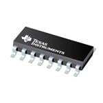
ICGOO在线商城 > 分立半导体产品 > 二极管 - 整流器 - 阵列 > UC3611DW
 Datasheet下载
- 型号: UC3611DW
- 制造商: Texas Instruments
- 库位|库存: xxxx|xxxx
- 要求:
| 数量阶梯 | 香港交货 | 国内含税 |
| +xxxx | $xxxx | ¥xxxx |
查看当月历史价格
查看今年历史价格
UC3611DW产品简介:
ICGOO电子元器件商城为您提供UC3611DW由Texas Instruments设计生产,在icgoo商城现货销售,并且可以通过原厂、代理商等渠道进行代购。 UC3611DW价格参考¥18.67-¥34.69。Texas InstrumentsUC3611DW封装/规格:二极管 - 整流器 - 阵列, Diode Array 4 Independent Schottky 50V 3A (DC) Surface Mount 16-SOIC (0.295", 7.50mm Width)。您可以下载UC3611DW参考资料、Datasheet数据手册功能说明书,资料中有UC3611DW 详细功能的应用电路图电压和使用方法及教程。
UC3611DW 是由 Texas Instruments(德州仪器)生产的一款双路高速 MOSFET 驱动器,虽然其主要功能不属于二极管或整流器,但在某些电源转换电路中会与功率器件配合使用。该芯片常用于同步整流、DC-DC 转换器、电机驱动及功率因数校正等场景。

在同步整流应用中,UC3611DW 可用于控制 N 沟道 MOSFET 替代传统二极管进行整流,提升效率;在开关电源中,它作为高边和低边驱动器,提供快速开关能力,支持高频工作,适用于推挽式、半桥或全桥拓扑结构。此外,在电机驱动系统中,UC3611DW 可用于驱动 H 桥电路中的 MOSFET,实现对直流电机的正反转控制。

该器件采用 16 引脚 SOIC 封装,具备较强的驱动能力和良好的抗干扰性能,适合工业电源、通信电源、不间断电源(UPS)、电动车控制器等高可靠性应用场景。

总结而言,UC3611DW 主要应用于需要高效、高频、高压 MOSFET 驱动的电力电子变换系统中,尤其适用于替代传统二极管以实现更高能效的场合。
| 参数 | 数值 |
| 产品目录 | |
| 描述 | DIODE SCHOTTKY 50V 3A 16SOIC肖特基二极管与整流器 Quad Schottky Diode Array |
| 产品分类 | 二极管,整流器 - 阵列分离式半导体 |
| 品牌 | Texas Instruments |
| 产品手册 | |
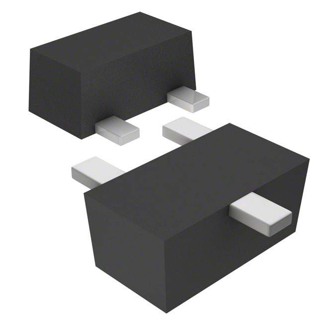
| 产品图片 |
|
| rohs | 符合RoHS无铅 / 符合限制有害物质指令(RoHS)规范要求 |
| 产品系列 | 二极管与整流器,肖特基二极管与整流器,Texas Instruments UC3611DW- |
| 数据手册 | http://www.ti.com/lit/pdf/slus338a |
| 产品型号 | UC3611DW |
| 不同If时的电压-正向(Vf) | 1.2V @ 1A |
| 不同 Vr时的电流-反向漏电流 | 100µA @ 40V |
| 二极管类型 | |
| 二极管配置 | 4 个独立式 |
| 产品 | Schottky Diodes |
| 产品目录页面 | |
| 产品种类 | 肖特基二极管与整流器 |
| 供应商器件封装 | 16-SOIC |
| 其它名称 | 296-11233-5 |
| 制造商产品页 | http://www.ti.com/general/docs/suppproductinfo.tsp?distId=10&orderablePartNumber=UC3611DW |
| 包装 | 管件 |
| 单位重量 | 473.700 mg |
| 反向恢复时间(trr) | 20ns |
| 商标 | Texas Instruments |
| 安装类型 | 表面贴装 |
| 安装风格 | SMD/SMT |
| 封装 | Tube |
| 封装/外壳 | 16-SOIC(0.295",7.50mm 宽) |
| 封装/箱体 | SOIC-16 |
| 峰值反向电压 | 50 V |
| 工作温度范围 | 0 C to + 70 C |
| 工厂包装数量 | 40 |
| 恢复时间 | 20 ns |
| 技术 | Silicon |
| 最大反向漏泄电流 | 100 uA |
| 最大工作温度 | + 70 C |
| 最小工作温度 | 0 C |
| 标准包装 | 40 |
| 正向电压下降 | 1.2 V at 1 A |
| 正向连续电流 | 3 A |
| 热阻 | - |
| 电压-DC反向(Vr)(最大值) | 50V |
| 电流-平均整流(Io)(每二极管) | 3A(DC) |
| 系列 | UC3611 |
| 速度 | 快速恢复 =< 500 ns,> 200mA(Io) |
| 配置 | Quad |

.jpg)


- 商务部:美国ITC正式对集成电路等产品启动337调查
- 曝三星4nm工艺存在良率问题 高通将骁龙8 Gen1或转产台积电
- 太阳诱电将投资9.5亿元在常州建新厂生产MLCC 预计2023年完工
- 英特尔发布欧洲新工厂建设计划 深化IDM 2.0 战略
- 台积电先进制程称霸业界 有大客户加持明年业绩稳了
- 达到5530亿美元!SIA预计今年全球半导体销售额将创下新高
- 英特尔拟将自动驾驶子公司Mobileye上市 估值或超500亿美元
- 三星加码芯片和SET,合并消费电子和移动部门,撤换高东真等 CEO
- 三星电子宣布重大人事变动 还合并消费电子和移动部门
- 海关总署:前11个月进口集成电路产品价值2.52万亿元 增长14.8%


PDF Datasheet 数据手册内容提取
(cid:1)(cid:2)(cid:3)(cid:4)(cid:3)(cid:3) (cid:1)(cid:2)(cid:5)(cid:4)(cid:3)(cid:3) SLUS338A – JUNE 1993 – REVISED MAY 2001 (cid:7)(cid:1)(cid:8)(cid:9) (cid:10)(cid:2)(cid:11)(cid:12)(cid:13)(cid:13)(cid:14)(cid:15) (cid:9)(cid:16)(cid:12)(cid:9)(cid:17) (cid:8)(cid:18)(cid:18)(cid:8)(cid:15) FEATURES DESCRIPTION (cid:1) Matched, Four-Diode Monolithic Array This four-diode array is designed for general (cid:1) High Peak Current purpose use as individual diodes or as a (cid:1) Low-Cost MINIDIP Package high-speed, high-current bridge. It is particularly (cid:1) useful on the outputs of high-speed power Low-Forward Voltage MOSFET drivers where Schottky diodes are (cid:1) Parallelable for Lower V or Higher I F F needed to clamp any negative excursions caused (cid:1) Fast Recovery Time by ringing on the driven line.These diodes are also (cid:1) Military Temperature Range Available ideally suited for use as voltage clamps when driving inductive loads such as relays and solenoids, and to provide a path for current free-wheeling in motor drive applications.The use of Schottky diode technology features high efficiency through lowered forward voltage drop and decreased reverse recovery time.This single monolithic chip is fabricated in both hermetic CERDIP and copper-eaded plastic packages. The UC1611 in ceramic is designed for –55°C to 125°C environments but with reduced peak current capability: while the UC3611 in plastic has higher current rating over a 0°C to 70°C ambient temperature range. AVAILABLE OPTIONS Packaged Devices TTA = TTJ SOIC Wide (DW) DIL (J) DIL (N) –55°C to 125°C UC1611DW UC1611J UC1611N 0°C to 70°C UC3611DW UC3611J UC3611N (cid:19)(cid:18)(cid:12)(cid:9)(cid:1)(cid:2)(cid:13)(cid:16)(cid:12)(cid:20) (cid:9)(cid:8)(cid:13)(cid:8) (cid:21)(cid:22)(cid:23)(cid:24)(cid:25)(cid:26)(cid:27)(cid:28)(cid:21)(cid:24)(cid:22) (cid:21)(cid:29) (cid:30)(cid:31)(cid:25)(cid:25) (cid:22)(cid:28) (cid:27)(cid:29) (cid:24)(cid:23) !(cid:31)"#(cid:21)(cid:30)(cid:27)(cid:28)(cid:21)(cid:24)(cid:22) $(cid:27)(cid:28) % Copyright 2001, Texas Instruments Incorporated (cid:19)(cid:25)(cid:24)$(cid:31)(cid:30)(cid:28)(cid:29) (cid:30)(cid:24)(cid:22)(cid:23)(cid:24)(cid:25)(cid:26) (cid:28)(cid:24) (cid:29)! (cid:30)(cid:21)(cid:23)(cid:21)(cid:30)(cid:27)(cid:28)(cid:21)(cid:24)(cid:22)(cid:29) ! (cid:25) (cid:28)& (cid:28) (cid:25)(cid:26)(cid:29) (cid:24)(cid:23) (cid:13) ’(cid:27)(cid:29) (cid:16)(cid:22)(cid:29)(cid:28)(cid:25)(cid:31)(cid:26) (cid:22)(cid:28)(cid:29) (cid:29)(cid:28)(cid:27)(cid:22)$(cid:27)(cid:25)$ ((cid:27)(cid:25)(cid:25)(cid:27)(cid:22)(cid:28))% (cid:19)(cid:25)(cid:24)$(cid:31)(cid:30)(cid:28)(cid:21)(cid:24)(cid:22) !(cid:25)(cid:24)(cid:30) (cid:29)(cid:29)(cid:21)(cid:22)* $(cid:24) (cid:29) (cid:22)(cid:24)(cid:28) (cid:22) (cid:30) (cid:29)(cid:29)(cid:27)(cid:25)(cid:21)#) (cid:21)(cid:22)(cid:30)#(cid:31)$ (cid:28) (cid:29)(cid:28)(cid:21)(cid:22)* (cid:24)(cid:23) (cid:27)## !(cid:27)(cid:25)(cid:27)(cid:26) (cid:28) (cid:25)(cid:29)% www.ti.com 1
(cid:1)(cid:2)(cid:3)(cid:4)(cid:3)(cid:3) (cid:1)(cid:2)(cid:5)(cid:4)(cid:3)(cid:3) SLUS338A – JUNE 1993 – REVISED MAY 2001 J OR N PACKAGE DW PACKAGE (TOP VIEW) (TOP VIEW) absolute maximum ratings over operating free-air temperature (unless otherwise noted)† Peak inverse voltage (per diode) . . . . . . . . . . . . . . . . . . . . . . . . . . . . . . . . . . . . . . . . . . . . . . . . . . . . . . . . . . . . . 50 V Diode-to-diode voltage . . . . . . . . . . . . . . . . . . . . . . . . . . . . . . . . . . . . . . . . . . . . . . . . . . . . . . . . . . . . . . . . . . . . . . 80 V Peak forward current UC1611 . . . . . . . . . . . . . . . . . . . . . . . . . . . . . . . . . . . . . . . . . . . . . . . . . . . . . . . . . . . . . . . . . . . . . . . . . . . . . . . . . 1 A UC3611 . . . . . . . . . . . . . . . . . . . . . . . . . . . . . . . . . . . . . . . . . . . . . . . . . . . . . . . . . . . . . . . . . . . . . . . . . . . . . . . . . 3 A Power dissipation at T = 70°C . . . . . . . . . . . . . . . . . . . . . . . . . . . . . . . . . . . . . . . . . . . . . . . . . . . . . . . . . . . . . . . 1 W A Storage temperature range, T . . . . . . . . . . . . . . . . . . . . . . . . . . . . . . . . . . . . . . . . . . . . . . . . . . . . –65°C to 150°C stg Lead temperature (soldering, 10 seconds) . . . . . . . . . . . . . . . . . . . . . . . . . . . . . . . . . . . . . . . . . . . . . . . . . . . 300°C †Stresses beyond those listed under “absolute maximum ratings” may cause permanent damage to the device. These are stress ratings only, and functional operation of the device at these or any other conditions beyond those indicated under “recommended operating conditions” is not implied. Exposure to absolute-maximum-rated conditions for extended periods may affect device reliability. ‡Please consult packaging section of data book for thermal limitations and considerations of package. electrical characteristics, all specifications apply to each individual diode, T = 25°C, T = T , J A J (except as noted) PARAMETER TEST CONDITIONS MIN TYP MAX UNITS IF = 100 mA 0.3 0.4 0.7 V FFoorrwaarrdd voollttaaggee ddrroopp IF = 1 A 0.9 1.2 V VR = 40 V 0.01 0.1 mA LLeeaakkaaggee ccuurrrreenntt VR = 40 V, TJ = 100°C 0.1 1.0 mA Reverse recovery 0.5 A forward to 0.5 A reverse 20 ns Forward recovery 1 A forward to 1.1 V recovery 40 ns Junction capacitance VR = 5V 100 pF NOTE: At forward currents of greater than 1.0 A, a parasitic current of approximately 10 mA may be collected by adjacent diodes. 2 www.ti.com
(cid:1)(cid:2)(cid:3)(cid:4)(cid:3)(cid:3) (cid:1)(cid:2)(cid:5)(cid:4)(cid:3)(cid:3) SLUS338A – JUNE 1993 – REVISED MAY 2001 APPLICATION INFORMATION REVERSE CURRENT FORWARD CURRENT vs vs VOLTAGE VOLTAGE 1000 5.0 500 3.0 2.0 300 200 1.0 µ– A 100 TJ = 125 °C – A 00..35 nt nt 0.2 e 50 e urr urr 0.1 TJ = –55 °C C 30 C e d 0.05 g 20 r a a Leak 10 Forw00..0023 TJ = 25 °C 0.01 5 T = 75 °C TJ = 25 °C J 0.005 3 0.003 TJ = 125 °C 2 0.002 1 0.001 0 10 20 30 40 50 0 0.2 0.4 0.6 0.8 1.0 1.2 1.4 1.6 1.8 2.0 Reverse Voltage – V Forward Voltage – V Figure 1 Figure 2 Figure 3. Clamp Diodes – PWMs and Drivers www.ti.com 3
(cid:1)(cid:2)(cid:3)(cid:4)(cid:3)(cid:3) (cid:1)(cid:2)(cid:5)(cid:4)(cid:3)(cid:3) SLUS338A – JUNE 1993 – REVISED MAY 2001 APPLICATION INFORMATION Figure 4. Transformer Coupled Drive Circuits Figure 5. Linear Regulations 4 www.ti.com
PACKAGE OPTION ADDENDUM www.ti.com 6-Feb-2020 PACKAGING INFORMATION Orderable Device Status Package Type Package Pins Package Eco Plan Lead/Ball Finish MSL Peak Temp Op Temp (°C) Device Marking Samples (1) Drawing Qty (2) (6) (3) (4/5) 5962-90538012A ACTIVE LCCC FK 20 1 TBD POST-PLATE N / A for Pkg Type -55 to 125 5962- 90538012A UC1611L/ 883B 5962-9053801PA ACTIVE CDIP JG 8 1 TBD Call TI N / A for Pkg Type -55 to 125 9053801PA UC1611 5962-9053801V2A ACTIVE LCCC FK 20 1 TBD POST-PLATE N / A for Pkg Type -55 to 125 5962- 9053801V2A UC1611L QMLV 5962-9053801VPA ACTIVE CDIP JG 8 1 TBD Call TI N / A for Pkg Type -55 to 125 9053801VPA UC1611 UC1611J ACTIVE CDIP JG 8 1 TBD Call TI N / A for Pkg Type -55 to 125 UC1611J UC1611J883B ACTIVE CDIP JG 8 1 TBD Call TI N / A for Pkg Type -55 to 125 9053801PA UC1611 UC1611L883B ACTIVE LCCC FK 20 1 TBD POST-PLATE N / A for Pkg Type -55 to 125 5962- 90538012A UC1611L/ 883B UC3611DW ACTIVE SOIC DW 16 40 Green (RoHS NIPDAU Level-2-260C-1 YEAR 0 to 70 UC3611DW & no Sb/Br) UC3611J ACTIVE CDIP JG 8 1 TBD Call TI N / A for Pkg Type 0 to 70 UC3611J UC3611N ACTIVE PDIP P 8 50 Green (RoHS NIPDAU N / A for Pkg Type 0 to 70 UC3611N & no Sb/Br) (1) The marketing status values are defined as follows: ACTIVE: Product device recommended for new designs. LIFEBUY: TI has announced that the device will be discontinued, and a lifetime-buy period is in effect. NRND: Not recommended for new designs. Device is in production to support existing customers, but TI does not recommend using this part in a new design. PREVIEW: Device has been announced but is not in production. Samples may or may not be available. OBSOLETE: TI has discontinued the production of the device. (2) RoHS: TI defines "RoHS" to mean semiconductor products that are compliant with the current EU RoHS requirements for all 10 RoHS substances, including the requirement that RoHS substance do not exceed 0.1% by weight in homogeneous materials. Where designed to be soldered at high temperatures, "RoHS" products are suitable for use in specified lead-free processes. TI may reference these types of products as "Pb-Free". Addendum-Page 1
PACKAGE OPTION ADDENDUM www.ti.com 6-Feb-2020 RoHS Exempt: TI defines "RoHS Exempt" to mean products that contain lead but are compliant with EU RoHS pursuant to a specific EU RoHS exemption. Green: TI defines "Green" to mean the content of Chlorine (Cl) and Bromine (Br) based flame retardants meet JS709B low halogen requirements of <=1000ppm threshold. Antimony trioxide based flame retardants must also meet the <=1000ppm threshold requirement. (3) MSL, Peak Temp. - The Moisture Sensitivity Level rating according to the JEDEC industry standard classifications, and peak solder temperature. (4) There may be additional marking, which relates to the logo, the lot trace code information, or the environmental category on the device. (5) Multiple Device Markings will be inside parentheses. Only one Device Marking contained in parentheses and separated by a "~" will appear on a device. If a line is indented then it is a continuation of the previous line and the two combined represent the entire Device Marking for that device. (6) Lead/Ball Finish - Orderable Devices may have multiple material finish options. Finish options are separated by a vertical ruled line. Lead/Ball Finish values may wrap to two lines if the finish value exceeds the maximum column width. Important Information and Disclaimer:The information provided on this page represents TI's knowledge and belief as of the date that it is provided. TI bases its knowledge and belief on information provided by third parties, and makes no representation or warranty as to the accuracy of such information. Efforts are underway to better integrate information from third parties. TI has taken and continues to take reasonable steps to provide representative and accurate information but may not have conducted destructive testing or chemical analysis on incoming materials and chemicals. TI and TI suppliers consider certain information to be proprietary, and thus CAS numbers and other limited information may not be available for release. In no event shall TI's liability arising out of such information exceed the total purchase price of the TI part(s) at issue in this document sold by TI to Customer on an annual basis. OTHER QUALIFIED VERSIONS OF UC1611, UC1611-SP, UC3611, UC3611M : •Catalog: UC3611, UC1611, UC3611M, UC3611 •Military: UC1611, UC1611 •Space: UC1611-SP NOTE: Qualified Version Definitions: •Catalog - TI's standard catalog product •Military - QML certified for Military and Defense Applications •Space - Radiation tolerant, ceramic packaging and qualified for use in Space-based application Addendum-Page 2
IMPORTANTNOTICEANDDISCLAIMER TI PROVIDES TECHNICAL AND RELIABILITY DATA (INCLUDING DATASHEETS), DESIGN RESOURCES (INCLUDING REFERENCE DESIGNS), APPLICATION OR OTHER DESIGN ADVICE, WEB TOOLS, SAFETY INFORMATION, AND OTHER RESOURCES “AS IS” AND WITH ALL FAULTS, AND DISCLAIMS ALL WARRANTIES, EXPRESS AND IMPLIED, INCLUDING WITHOUT LIMITATION ANY IMPLIED WARRANTIES OF MERCHANTABILITY, FITNESS FOR A PARTICULAR PURPOSE OR NON-INFRINGEMENT OF THIRD PARTY INTELLECTUAL PROPERTY RIGHTS. These resources are intended for skilled developers designing with TI products. You are solely responsible for (1) selecting the appropriate TI products for your application, (2) designing, validating and testing your application, and (3) ensuring your application meets applicable standards, and any other safety, security, or other requirements. These resources are subject to change without notice. TI grants you permission to use these resources only for development of an application that uses the TI products described in the resource. Other reproduction and display of these resources is prohibited. No license is granted to any other TI intellectual property right or to any third party intellectual property right. TI disclaims responsibility for, and you will fully indemnify TI and its representatives against, any claims, damages, costs, losses, and liabilities arising out of your use of these resources. TI’s products are provided subject to TI’s Terms of Sale (www.ti.com/legal/termsofsale.html) or other applicable terms available either on ti.com or provided in conjunction with such TI products. TI’s provision of these resources does not expand or otherwise alter TI’s applicable warranties or warranty disclaimers for TI products. Mailing Address: Texas Instruments, Post Office Box 655303, Dallas, Texas 75265 Copyright © 2020, Texas Instruments Incorporated