ICGOO在线商城 > 集成电路(IC) > PMIC - 稳压器 - DC DC 切换控制器 > UC3525ADW
 Datasheet下载
- 型号: UC3525ADW
- 制造商: Texas Instruments
- 库位|库存: xxxx|xxxx
- 要求:
| 数量阶梯 | 香港交货 | 国内含税 |
| +xxxx | $xxxx | ¥xxxx |
查看当月历史价格
查看今年历史价格
UC3525ADW产品简介:
ICGOO电子元器件商城为您提供UC3525ADW由Texas Instruments设计生产,在icgoo商城现货销售,并且可以通过原厂、代理商等渠道进行代购。 UC3525ADW价格参考¥10.89-¥19.45。Texas InstrumentsUC3525ADW封装/规格:PMIC - 稳压器 - DC DC 切换控制器, 降压,升压,反激,正激转换器,全桥,半桥,推挽 稳压器 正 输出 升压,降压,升压/降压 DC-DC 控制器 IC 16-SOIC。您可以下载UC3525ADW参考资料、Datasheet数据手册功能说明书,资料中有UC3525ADW 详细功能的应用电路图电压和使用方法及教程。
UC3525ADW 是 Texas Instruments(德州仪器)生产的一款双端 PWM 控制器,常用于 DC-DC 转换器和开关电源设计中。它属于 PMIC(电源管理集成电路)中的稳压器类别,具体为 DC-DC 切换控制器。

 主要应用场景包括:

1. 开关电源(SMPS):广泛用于各类开关电源中,如适配器、电源模块、工业电源等,用于控制 MOSFET 或双极型晶体管的导通与关断,实现高效电能转换。

2. DC-DC 转换器设计:适用于升压(Boost)、降压(Buck)、反激(Flyback)、正激(Forward)等拓扑结构的 DC-DC 电源转换系统,尤其适合需要精确电压调节和稳定输出的应用。

3. 工业控制系统:用于工业自动化设备中的电源模块,提供稳定的电压输出,确保控制系统可靠运行。

4. 通信设备电源:在通信基站、路由器、交换机等设备中,用于构建高效率、高稳定性的电源系统。

5. 电机驱动电源:在需要可控电源输出的电机驱动系统中,UC3525ADW 可用于构建高效的驱动电源。

6. 电池充电器:用于设计智能电池充电器,实现恒流恒压充电控制,适用于铅酸电池、锂电池等充电方案。

该芯片具有内置振荡器、误差放大器、软启动功能和过流保护功能,适合多种电源控制应用,具备较高的灵活性和可靠性。
| 参数 | 数值 |
| 产品目录 | 集成电路 (IC)半导体 |
| Cuk | 无 |
| 描述 | IC REG CTRLR BST FLYBK VM 16SOIC开关控制器 Regulating PWM |
| 产品分类 | |
| 品牌 | Texas Instruments |
| 产品手册 | |
| 产品图片 |
|
| rohs | 符合RoHS无铅 / 符合限制有害物质指令(RoHS)规范要求 |
| 产品系列 | 电源管理 IC,开关控制器 ,Texas Instruments UC3525ADW- |
| 数据手册 | |
| 产品型号 | UC3525ADW |
| PWM类型 | 电压模式 |
| 上升时间 | 100 ns |
| 下降时间 | 50 ns |
| 产品目录页面 | |
| 产品种类 | 开关控制器 |
| 倍增器 | 无 |
| 其它名称 | 296-11215-5 |
| 分频器 | 无 |
| 包装 | 管件 |
| 升压 | 是 |
| 单位重量 | 473.700 mg |
| 占空比 | 45% |
| 占空比-最大 | 50 % |
| 反向 | 无 |
| 反激式 | 是 |
| 同步管脚 | Yes |
| 商标 | Texas Instruments |
| 安装风格 | SMD/SMT |
| 封装 | Tube |
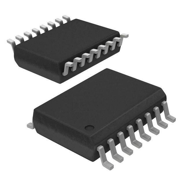
| 封装/外壳 | 16-SOIC(0.295",7.50mm 宽) |
| 封装/箱体 | SOIC-16 Wide |
| 工作温度 | 0°C ~ 70°C |
| 工作电源电压 | 8 V to 35 V |
| 工厂包装数量 | 40 |
| 开关频率 | 450 kHz |
| 拓扑结构 | Buck, Boost, Flyback, Forward, Full-Bridge, Half-Bridge, Push-Pull |
| 最大工作温度 | + 70 C |
| 最小工作温度 | 0 C |
| 标准包装 | 40 |
| 电压-电源 | 8 V ~ 35 V |
| 类型 | Voltage Mode PWM Controllers |
| 系列 | UC3525A |
| 输出数 | 2 |
| 输出电压 | 35.00 V |
| 输出电流 | 400 mA |
| 输出端数量 | 2 Output |
| 降压 | 无 |
| 隔离式 | 无 |
| 频率-最大值 | 400kHz |

.jpg)


- 商务部:美国ITC正式对集成电路等产品启动337调查
- 曝三星4nm工艺存在良率问题 高通将骁龙8 Gen1或转产台积电
- 太阳诱电将投资9.5亿元在常州建新厂生产MLCC 预计2023年完工
- 英特尔发布欧洲新工厂建设计划 深化IDM 2.0 战略
- 台积电先进制程称霸业界 有大客户加持明年业绩稳了
- 达到5530亿美元!SIA预计今年全球半导体销售额将创下新高
- 英特尔拟将自动驾驶子公司Mobileye上市 估值或超500亿美元
- 三星加码芯片和SET,合并消费电子和移动部门,撤换高东真等 CEO
- 三星电子宣布重大人事变动 还合并消费电子和移动部门
- 海关总署:前11个月进口集成电路产品价值2.52万亿元 增长14.8%


PDF Datasheet 数据手册内容提取
Product Order Technical Tools & Support & Folder Now Documents Software Community UC1525A,UC1527A,UC2525A UC2527A,UC3525A,UC3527A SLUS191D–FEBRUARY1997–REVISEDJULY2017 UCx52xA Regulating Pulse Width Modulators 1 Features 3 Description • 8-Vto35-VOperation The UC1525A/1527A series of pulse width modulator 1 integrated circuits are designed to offer improved • 5.1-VReferenceTrimmedto1% performance and lowered external parts count when • 100-Hzto500-kHzOscillatorRange used in designing all types of switching power • SeparateOscillatorSyncTerminal supplies. The on-chip 5.1-V reference is trimmed to 1% and the input common-mode range of the error • AdjustableDead-TimeControl amplifier includes the reference voltage, eliminating • InternalSoftStart external resistors. A sync input to the oscillator allows • Pulse-by-PulseShutdown multiple units to be slaved or a single unit to be synchronized to an external system clock. A single • InputUndervoltageLockoutWithHysteresis resistor between C and the discharge terminals • LatchingPWMtoPreventMultiplePulses T provides a wide range of dead-time adjustment. • DualSourceandSinkOutputDrivers These devices also feature built-in soft-start circuitry with only an external timing capacitor required. A 2 Applications shutdown terminal controls both the soft-start circuitry and the output stages, providing instantaneous turn • Off-LineandDC/DCPowerSupplies off through the PWM latch with pulsed shutdown, as • ConvertersUsingVoltageMode well as soft-start recycle with longer shutdown • Single-EndedorTwo-SwitchTopologyDesigns commands. • SolarInverters DeviceInformation(1) • WeldingInverters PARTNUMBER PACKAGE BODYSIZE(NOM) • MotorControl LCCC(20) 8.89mm×8.89mm • BatteryChargers CDIP(16) 19.56mm×6.67mm UCx52xA SOIC(16) 10.30mm×7.50mm BlockDiagram PDIP(16) 19.30mm×6.35mm OSC VREFOUT PLCC(20) 8.96mm×8.96mm 16 4 13 VC (1) For all available packages, see the orderable addendum at +VIN15 RReefgeurelantcoer LUoVckLoOu t NOR 11 OUTPUT A theendofthedatasheet. GROUND12 To Internal SYNC 3 Circutry RCTT 65 OSC FFlloipp NOR 14 OUTPUT B DISCHARGE 7 UC1525A Output Stage S R 13 VC COMPENSATION 9 PWM INV INPUT 1 EArmropr VREF S Latch OR 11 OUTPUT A NI INPUT 2 50 µA SOFTSTART 8 3 k(cid:159) OR SHUTDOWN10 14 OUTPUT B 5 k(cid:159) UOCut1p5u2t 7SAtage Copyright © 2017, Texas Instruments Incorporated 1 An IMPORTANT NOTICE at the end of this data sheet addresses availability, warranty, changes, use in safety-critical applications, intellectualpropertymattersandotherimportantdisclaimers.PRODUCTIONDATA.
UC1525A,UC1527A,UC2525A UC2527A,UC3525A,UC3527A SLUS191D–FEBRUARY1997–REVISEDJULY2017 www.ti.com Table of Contents 1 Features.................................................................. 1 7.4 DeviceFunctionalModes..........................................9 2 Applications........................................................... 1 8 ApplicationandImplementation........................ 10 3 Description............................................................. 1 8.1 ApplicationInformation............................................10 4 RevisionHistory..................................................... 2 8.2 TypicalApplication .................................................10 5 PinConfigurationandFunctions......................... 3 9 PowerSupplyRecommendations...................... 16 6 Specifications......................................................... 4 10 Layout................................................................... 16 6.1 AbsoluteMaximumRatings......................................4 10.1 LayoutGuidelines.................................................16 6.2 ESDRatings..............................................................4 10.2 LayoutExample....................................................16 6.3 RecommendedOperatingConditions.......................4 11 DeviceandDocumentationSupport................. 17 6.4 ThermalInformation..................................................5 11.1 DocumentationSupport .......................................17 6.5 ElectricalCharacteristics...........................................5 11.2 RelatedLinks........................................................17 6.6 TypicalCharacteristics..............................................7 11.3 CommunityResources..........................................17 7 DetailedDescription.............................................. 8 11.4 Trademarks...........................................................17 7.1 Overview...................................................................8 11.5 ElectrostaticDischargeCaution............................17 7.2 FunctionalBlockDiagram.........................................8 11.6 Glossary................................................................17 7.3 FeatureDescription...................................................9 12 Mechanical,Packaging,andOrderable Information........................................................... 17 4 Revision History ChangesfromRevisionC(January2008)toRevisionD Page • AddedESDRatingstable,FeatureDescriptionsection,DeviceFunctionalModes,ApplicationandImplementation section,PowerSupplyRecommendationssection,Layoutsection,DeviceandDocumentationSupportsection,and Mechanical,Packaging,andOrderableInformationsection ................................................................................................. 1 • AddedThermalInformationtable........................................................................................................................................... 5 • ChangedR valuesintheThermalInformationtable:from80-120toN/AforJ;from90to47.6forN;from45-90to θJA 72.6forDW;from43-75to55.8forFN;andfrom70-80toN/AforFK ................................................................................ 5 • ChangedR valuesintheThermalInformationtable:from28to37.4(top)and10.1(bottom)forJ;from45to37.3 θJC (top)forN;from25to34(top)forDW;from34to33.7(top)forFN;andfrom20to32.9(top)to3.5(bottom)forFK ...... 5 2 SubmitDocumentationFeedback Copyright©1997–2017,TexasInstrumentsIncorporated ProductFolderLinks:UC1525A UC1527A UC2525AUC2527A UC3525A UC3527A
UC1525A,UC1527A,UC2525A UC2527A,UC3525A,UC3527A www.ti.com SLUS191D–FEBRUARY1997–REVISEDJULY2017 5 Pin Configuration and Functions JandNPackage 16-PinCDIPandPDIP FNandFKPackages TopView 20-PinPLCCorLCCC TopView INVInput 1 16 VREF ut put p n NSIIYnNpuCt 23 1154 +OVuItNput B NIIn INVI NC VREF +VIN OSC Output 4 13 VC 3 2 1 20 19 CT 5 12 Ground SYNC 4 18 Output B RT 6 11 Output A OSC Output 5 17 VC Discharge 7 10 Shutdown NC 6 16 NC SoftStart 8 9 Compensation CT 7 15 Ground RT 8 14 OutputA 9 10 11 12 13 Discharge SoftStart NC pensation Shutdown m o C PinFunctions PIN CDIP, PLCC, I/O DESCRIPTION NAME PDIP LCCC INVInput 1 2 I Invertinginputtotheerroramplifier NIInput 2 3 I Noninvertinginputtotheerroramplifier SYNC 3 4 I Oscillatorsyncterminal OSCOutput 4 5 O Oscillatorfrequencyoutput Timingcapacitorconnectionpinforoscillatorfrequencyprogramming.The C 5 7 I timingcapacitorshouldbeconnectedtothedevicegroundusingminimaltrace T length. R 6 8 I Timingresistorconnectionpinforoscillatorfrequencyprogramming T AsingleresistorbetweenC andthedischargeterminalsprovidesdead-time Discharge 7 9 I T adjustment SoftStart 8 10 I Soft-startinputpin. Compensati 9 12 O Outputoftheerroramplifierforcompensation on Shutdown 10 13 I PullthispinhightoshutdownPWMoutput OutputA 11 14 O outputAoftheon-chipdrivestage Ground 12 15 — Groundreturnpin Powersupplypinfortheoutputstage.Thispinshouldbebypassedwitha V 13 17 — C 0.1-µFmonolithicceramiclowESLcapacitorwithminimaltracelengths. OutputB 14 18 O OutputBoftheon-chipdrivestage. +V 15 19 — Inputvoltage IN 5.1-Vreference.Forstability,thereferenceshouldbebypassedwitha0.1-µF V 16 20 O monolithicceramiclowESLcapacitorandminimaltracelengthtotheground REF plane. NC — 1,6,11,16 — Nointernalconnection Copyright©1997–2017,TexasInstrumentsIncorporated SubmitDocumentationFeedback 3 ProductFolderLinks:UC1525A UC1527A UC2525AUC2527A UC3525A UC3527A
UC1525A,UC1527A,UC2525A UC2527A,UC3525A,UC3527A SLUS191D–FEBRUARY1997–REVISEDJULY2017 www.ti.com 6 Specifications 6.1 Absolute Maximum Ratings overoperatingfree-airtemperaturerange(unlessotherwisenoted)(1) MIN MAX UNIT +V Supplyvoltage 40 V IN V Collectorsupplyvoltage 40 V C Logicinputs –0.3 5.5 V Analoginputs –0.3 +V V IN Outputcurrent,sourceorsink 500 mA Referenceoutputcurrent 50 mA Oscillatorchargingcurrent 5 mA PowerdissipationatT =+25°C(2) 1000 mW A PowerdissipationatT =+25°C(2) 2000 mW C Operatingjunctiontemperature –55 150 °C Leadtemperature(soldering,10seconds) 300 °C T Storagetemperature –65 150 °C stg (1) StressesbeyondthoselistedunderAbsoluteMaximumRatingsmaycausepermanentdamagetothedevice.Thesearestressratings only,whichdonotimplyfunctionaloperationofthedeviceattheseoranyotherconditionsbeyondthoseindicatedunderRecommended OperatingConditions.Exposuretoabsolute-maximum-ratedconditionsforextendedperiodsmayaffectdevicereliability. 6.2 ESD Ratings VALUE UNIT Human-bodymodel(HBM),perANSI/ESDA/JEDECJS-001(1) 3000 V Electrostaticdischarge V (ESD) Charged-devicemodel(CDM),perJEDECspecificationJESD22-C101(2) 1500 (1) JEDECdocumentJEP155statesthat500-VHBMallowssafemanufacturingwithastandardESDcontrolprocess. (2) JEDECdocumentJEP157statesthat250-VCDMallowssafemanufacturingwithastandardESDcontrolprocess. 6.3 Recommended Operating Conditions overoperatingfree-airtemperaturerange(unlessotherwisenoted) MIN MAX UNIT +V Inputvoltage 8 35 V IN V Collectorsupplyvoltage 4.5 35 V C Sink/sourceloadcurrent(steadystate) 0 100 mA Sink/sourceloadcurrent(peak) 0 400 mA Referenceloadcurrent 0 20 mA Oscillatorfrequencyrange 100 400 Hz Oscillatortimingresistor 2 150 kΩ Oscillatortimingcapacitor 0.001 0.01 µF Deadtimeresistorrange 0 500 Ω UC1525A,UC1527A –55 125 Operatingambienttemperature UC2525A,UC2527A –25 85 °C UC3525A,UC3527A 0 70 4 SubmitDocumentationFeedback Copyright©1997–2017,TexasInstrumentsIncorporated ProductFolderLinks:UC1525A UC1527A UC2525AUC2527A UC3525A UC3527A
UC1525A,UC1527A,UC2525A UC2527A,UC3525A,UC3527A www.ti.com SLUS191D–FEBRUARY1997–REVISEDJULY2017 6.4 Thermal Information UCx52xA THERMALMETRIC(1) FK J DW N FN UNIT (LCCC) (CDIP) (SOIC) (PDIP) (PLCC) 20PINS 16PINS 16PINS 16PINS 20PINS R Junction-to-ambientthermalresistance N/A N/A 72.6 47.6 55.8 °C/W θJA R Junction-to-case(top)thermalresistance 32.9 37.4 34 37.3 33.7 °C/W θJC(top) R Junction-to-boardthermalresistance 32.1 54.2 37.3 27.7 21.1 °C/W θJB ψ Junction-to-topcharacterizationparameter N/A N/A 8.9 17.3 9.7 °C/W JT ψ Junction-to-boardcharacterizationparameter N/A N/A 36.8 27.5 20.8 °C/W JB R Junction-to-case(bottom)thermalresistance 3.5 10.1 N/A N/A N/A °C/W θJC(bot) (1) Formoreinformationabouttraditionalandnewthermalmetrics,seetheSemiconductorandICPackageThermalMetricsapplication report. 6.5 Electrical Characteristics overoperatingfree-airtemperaturerange(unlessotherwisenoted) PARAMETER TESTCONDITIONS MIN TYP MAX UNIT REFERENCE UC152xA, 5.05 5.1 5.15 Outputvoltage T =25°C UC252xA V J UC352xA 5 5.1 5.2 Lineregulation V =8Vto35V 10 20 mV IN Loadregulation I =0mAto20mA 20 50 mV L Temperaturestability(1) Overoperating 20 50 mV UC152xA, 5 5.2 Totaloutputvariation(1) Line,load,andtemperature UC252xA V UC352xA 4.95 5.25 Shortercircuitcurrent V =0,T =25°C 80 100 mA REF J OutputnoiseVoltage(1) 10Hz≤10kHz,T =25°C 40 200 µVrms J Long-termstability(1) T =125°C 20 50 mV J OSCILLATORSECTION(2) Initialaccuracy(1)(2) T =25°C 2% 6% J UC152xA, 0.3% 1% Voltagestability(1)(2) V =8Vto35V UC252xA IN UC352xA 1% 2% Temperaturestability(1) Overoperating 3% 6% Minimumfrequency R =200kΩ,C =0.1mF 120 Hz T T Maximumfrequency R =2kΩ,C =470pF 400 kHz T T Currentmirror I =2mA 1.7 2 2.2 mA RT Clockamplitude(1)(2) 3 3.5 V Clockwidth(1)(2) T =25°C 0.3 0.5 1 µs J Syncronizationthreshold(1)(2) 1.2 2 2.8 V Syncinputcurrent Syncvoltage=3.5V 1 2.5 mA ERRORAMPLIFIERSECTION(V =5.1V) CM UC152xA,UC252xA 0.5 5 mV Inputoffsetvoltage UC352xA 2 10 (1) Theseparameters,althoughensuredovertherecommendedoperatingconditions,arenot100%testedinproduction. (2) Testedatf =40kHz(R =3.6kΩ,C =0.01mF,R =0.Approximateoscillatorfrequencyisdefinedby OSC 1 T T D f = C (0.7R +3R ) T T D . Copyright©1997–2017,TexasInstrumentsIncorporated SubmitDocumentationFeedback 5 ProductFolderLinks:UC1525A UC1527A UC2525AUC2527A UC3525A UC3527A
UC1525A,UC1527A,UC2525A UC2527A,UC3525A,UC3527A SLUS191D–FEBRUARY1997–REVISEDJULY2017 www.ti.com Electrical Characteristics (continued) overoperatingfree-airtemperaturerange(unlessotherwisenoted) PARAMETER TESTCONDITIONS MIN TYP MAX UNIT Inputbiascurrent 1 10 µA Inputoffsetcurrent 1 DCopenloopgain R ≥10MΩ 60 75 dB L Gain-bandwidthproduct(1) A =0dB,T =25°C 1 2 MHz V J DCtransconductance(1)(3) T =25°C,30kΩ≤R ≤1MΩ 1.1 1.5 mS J L Low-leveloutputvoltage 0.2 0.5 V High-leveloutputvoltage 3.8 5.6 Commonmoderejection V =1.5Vto5.2V 60 75 CM dB Supplyvoltagerejection V =8Vto35V 50 60 IN PWMCOMPARATOR Minimumduty-cycle 0% Maximumduty-cycle 45% 49% Zeroduty-cycle 0.7 0.9 Inputthreshold(4) V Maximumduty-cycle 3.3 3.6 Inputbiascurrent(4) 0.05 1 µA SHUTDOWN Soft-startcurrent V =0V,V =0V 25 50 80 µA SD SS Soft-startlowlevel V =2.5V 0.4 0.7 SD V Shutdownthreshold Tooutputs,V =5.1V,T =25°C 0.6 0.8 1 SS J Shutdowninputcurrent V =2.5V 0.4 1 mA SD ShutdownDelay(5) V =2.5V,T =25°C 0.2 0.5 µS SD J OUTPUTDRIVERS(EACHOUTPUT)(V =20V) C I =20mA 0.2 0.4 SINK Low-leveloutputvoltage V I =100mA 1 2 SINK I =20mA 18 19 SOURCE High-leveloutputvoltage V I =100mA 17 18 SOURCE Undervoltagelockout V andV =High 6 7 8 V COMP SS V OFFcurrent(6) V =35V 200 µA C C Risetime(5) C =1nF,T =25°C 100 600 L J ns Falltime(5) C =1nF,T =25°C 50 300 L J TOTALSTANDBYCURRENT Supplycurrent V =35V 14 20 mA IN (3) DCtransconductance(g )relatestoDCopen-loopvoltagegain(A )accordingtothefollowingequation:A =gMRLwhereR isthe M V V L resistancefrompin9toground.Theminimumg specificationisusedtocalculateminimumA whentheerroramplifieroutputis M V loaded. (4) Testedatf =40kHz(R =3.6kΩ,C =0.01mF,R =0Ω. OSC T T D (5) Theseparameters,althoughensuredovertherecommendedoperatingconditions,arenot100%testedinproduction. (6) Collectoroff-statequiescentcurrentmeasuredatpin13withoutputslowforUC1525AandhighforUC1527A. 6 SubmitDocumentationFeedback Copyright©1997–2017,TexasInstrumentsIncorporated ProductFolderLinks:UC1525A UC1527A UC2525AUC2527A UC3525A UC3527A
UC1525A,UC1527A,UC2525A UC2527A,UC3525A,UC3527A www.ti.com SLUS191D–FEBRUARY1997–REVISEDJULY2017 6.6 Typical Characteristics 200 500 100 CT = 0.1 PF CT = .05 PF ng Resistance (k): 01.011 CCTT == 00..0015 PPFF Time Resistance (): 234000000 CCCCCTTTTT ===== ..52100 nnn21FFF PPFF Timi 0.01 CCCTTT === 005.. 01n2 FP PFF Dead 100 0.001 CT = 2 nF CT = 1 nF 0.0002 0 1P 10P 100P 1m 10m 100m 0.1 1 10 100 200 Charge Time (s) Charge Time (Ps) D002 D003 Figure1.OscillatorChargeTimevsRTandCT Figure2.OscillatorDischargeTimevsRTCT 500 100 800 Voltage Gain RL = 30 k: D 400 B) 80 RL = 100 k: 600 m Recommended R 230000 op Voltage Gain (d 4600 RRRVPohLLL la===tas egf31e0 M 0P :kh:ase 240000 qn-Loop Phase () Maximu 100 -55 qC Open-Lo 200 0-200 Ope 25 qC 125 qC 0 -20 -400 2 4 6 8 10 12 10 100 1k 10k 100k 1M 10M Minimum Recommended (RT - k:) D004 Frequency (Hz) D005 Figure3.MaximumValueR vsMinimumValueR Figure4.ErrorAmplifierVoltageGainandPhasevs D T Frequency Copyright©1997–2017,TexasInstrumentsIncorporated SubmitDocumentationFeedback 7 ProductFolderLinks:UC1525A UC1527A UC2525AUC2527A UC3525A UC3527A
UC1525A,UC1527A,UC2525A UC2527A,UC3525A,UC3527A SLUS191D–FEBRUARY1997–REVISEDJULY2017 www.ti.com 7 Detailed Description 7.1 Overview The UCx52xA series of pulse width modulator integrated circuits are designed to offer improved performance and lowered external parts count when used in designing all types of switching power supplies. The on-chip 5.1-V reference is trimmed to 1% and the input common-mode range of the error amplifier includes the reference voltage, eliminating external resistors. A sync input to the oscillator allows multiple units to be slaved or a single unit to be synchronized to an external system clock. A single resistor between CT and the discharge terminals providesawiderangeofdead-timeadjustment.Thesedevicesalsofeaturebuilt-insoft-startcircuitrywithonlyan external timing capacitor required. A shutdown terminal controls both the soft-start circuitry and the output stages, providing instantaneous turn off through the PWM latch with pulsed shutdown, as well as soft-start recyclewithlongershutdowncommands. These functions are also controlled by an undervoltage lockout which keeps the outputs off and the soft-start capacitor discharged for subnormal input voltages. This lockout circuitry includes approximately 500 mV of hysteresis for jitter-free operation. Another feature of these PWM circuits is a latch following the comparator. Once a PWM pulse has been terminated for any reason, the outputs will remain off for the duration of the period. Thelatchisresetwitheachclockpulse.Theoutputstagesaretotem-poledesignscapableofsourcingorsinking inexcessof200mA.TheUC1525AoutputstagefeaturesNORlogic,givingaLOWoutputforanOFFstate.The UC1527AusesORlogic,whichresultsinaHIGHoutputlevelwhenOFF. 7.2 Functional Block Diagram OSC VREF OUT 16 4 13 VC NOR Reference UVLO +VIN 15 Regulator Lockout 11 OUTPUT A GROUND 12 To Internal SYNC 3 Circutry RT 6 OSC Flip NOR CT 5 Flop 14 OUTPUT B DISCHARGE 7 UC1525A Output Stage S R 13 VC COMPENSATION 9 PWM Error Latch OR Amp VREF INV INPUT 1 S 11 OUTPUT A NI INPUT 2 50 µA SOFTSTART 8 3 k(cid:159) OR SHUTDOWN 10 14 OUTPUT B UC1527A 5 k(cid:159) Output Stage Copyright © 2017, Texas Instruments Incorporated 8 SubmitDocumentationFeedback Copyright©1997–2017,TexasInstrumentsIncorporated ProductFolderLinks:UC1525A UC1527A UC2525AUC2527A UC3525A UC3527A
UC1525A,UC1527A,UC2525A UC2527A,UC3525A,UC3527A www.ti.com SLUS191D–FEBRUARY1997–REVISEDJULY2017 7.3 Feature Description 7.3.1 AdjustableDead-TimeControl AsingleresistorbetweenCTandthedischargeterminalsprovidesawiderangeofdead-timeadjustment. 7.3.2 SoftStart Soft start is achieved by connecting the soft-start pin to ground through a capacitor, charged by the 50-µA currentsource.SeeFunctionalBlockDiagram. 7.3.3 InputUndervoltageLockoutWithHysteresis The undervoltage lockout keeps the outputs off and the soft-start capacitor discharged for subnormal input voltages.Thislockoutcircuitryincludesapproximately500mVofhysteresisforjitter-freeoperation. 7.3.4 ShutdownandPulse-by-PulseCurrentLimiting SeeShutdownOptions(SeeFunctionalBlockDiagram). 7.4 Device Functional Modes Thisdevicehasnofunctionalmodes. 7.4.1 ShutdownOptions(SeeFunctionalBlockDiagram) Since both the compensation and soft-start terminals have current source pullups, either can readily accept a pull-down signal which only has to sink a maximum of 100 A to turn off the outputs. This is subject to the added requirementofdischargingwhateverexternalcapacitancemaybeattachedtothesepins. An alternate approach is the use of the shutdown circuitry of the shutdown pin which has been improved to enhance the available shutdown options. Activating this circuit by applying a positive signal on the shutdown pin performs two functions; the PWM latch is immediately set providing the fastest turn-off signal to the outputs; and a 150-A current sink begins to discharge the external soft-start capacitor. If the shutdown command is short, the PWM signal is terminated without significant discharge of the soft-start capacitor, thus, allowing, for example, a convenientimplementationofpulse-by-pulsecurrentlimiting.Holdingtheshutdownpinhighforalongerduration, however,willultimatelydischargethisexternalcapacitor,recyclingslowturnonuponrelease. The shutdown pin should not be left floating as noise pickup could conceivably interrupt normal operation. All transitions of the voltage on the shutdown pin should be within the time frame of one clock cycle and not repeatedatafrequencyhigherthan10clockcycles. Copyright©1997–2017,TexasInstrumentsIncorporated SubmitDocumentationFeedback 9 ProductFolderLinks:UC1525A UC1527A UC2525AUC2527A UC3525A UC3527A
UC1525A,UC1527A,UC2525A UC2527A,UC3525A,UC3527A SLUS191D–FEBRUARY1997–REVISEDJULY2017 www.ti.com 8 Application and Implementation NOTE Information in the following applications sections is not part of the TI component specification, and TI does not warrant its accuracy or completeness. TI’s customers are responsible for determining suitability of components for their purposes. Customers should validateandtesttheirdesignimplementationtoconfirmsystemfunctionality. 8.1 Application Information The UC1525A/1527A series of pulse width modulator integrated circuits are designed to offer improved performance and lowered external parts count when used in designing all types of switching power supplies. The UC1525A output stage features NOR logic, giving a LOW output for an OFF state. The UC1527A utilizes OR logicwhichresultsinaHIGHoutputlevelwhenOFF. 8.2 Typical Application V REF Reference 16 Regulator 15 +VIN Clock 0.1 0.1 3kW 4 Flip/ 13 VC PWM Flop Adj. SYNC 0.1 10kW 3 A 11 R T OutA 1.5kW 3.6kW Deadtime 6 cillator 1k(,21)W .009 Ramp Os 7 100W B 14 5 Comp CT .001 OutB 0.1 9 PWM 1=VOS 10kW 0.1 50mA 12 GND 2 = I ( + ) 3=I (−) 8 Soft-Start + 1 1 5mF 2 2 1 5kW 5kW − E/A 5kW 10 VREF 3 3 2 Shutdown V/IMeter + 1 1 2 2 D.U.T. 3 3 Copyright©2017,TexasInstrumentsIncorporated Figure5. LabTestFixture 10 SubmitDocumentationFeedback Copyright©1997–2017,TexasInstrumentsIncorporated ProductFolderLinks:UC1525A UC1527A UC2525AUC2527A UC3525A UC3527A
UC1525A,UC1527A,UC2525A UC2527A,UC3525A,UC3527A www.ti.com SLUS191D–FEBRUARY1997–REVISEDJULY2017 Typical Application (continued) 8.2.1 TheoryofOperation +V SUPPLY Q1 T1 C1 13 R1 T2 +V C A 11 UC1525A Q2 30W B 14 GND C2 R2 12 Return Figure6. LowPowerTransformers Low power transformers can be driven by the UC1525A. Automatic reset occurs during dead time, when both endsoftheprimarywindingareswitchedtoground. VREF 16 Q1 Q5 Q8 7.4kW RT 6 Q3 CT 5 Q6 Q9 2kW 14kW RampToPWM Q10 Q11 Q14 2kW 25kW SYNC 3 DISCHARGE 7 400mA 5pF BlankingToOutout 23kW Q4 Q2 Q7 1kW Q12 Q13 3kW 250kW 1kW GND 12 4 Clock Figure7. UC1525AOscillatorSchematic Copyright©1997–2017,TexasInstrumentsIncorporated SubmitDocumentationFeedback 11 ProductFolderLinks:UC1525A UC1527A UC2525AUC2527A UC3525A UC3527A
UC1525A,UC1527A,UC2525A UC2527A,UC3525A,UC3527A SLUS191D–FEBRUARY1997–REVISEDJULY2017 www.ti.com Typical Application (continued) 15 +VIN Q3 Q4 Q1 Q2 InvInput 1 toPWM Comparator NIInput 2 5.8V 100W 200mA 100mA 9 Comp Figure8. UC1525AErrorAmplifier +VIN 13 +VC Q5 Q7 Q9 Q4 Q10 5 K 11 Output +V 14 REF Q8 Q6 Q11 Q6Ommitted InUC1527A Q1 Q2 Q3 2kW 5kW 10kW 10kW Clock F/F PWM Figure9. UC1525AOutputCircuit(1/2circuitshown) +V Q1 ToOutputFilter SUPPLY R1 R2 13 +V C A 11 UC1525A B 14 GND 12 Return Figure10. GroundedDriverOutputsForSingle-EndedSupplies 12 SubmitDocumentationFeedback Copyright©1997–2017,TexasInstrumentsIncorporated ProductFolderLinks:UC1525A UC1527A UC2525AUC2527A UC3525A UC3527A
UC1525A,UC1527A,UC2525A UC2527A,UC3525A,UC3527A www.ti.com SLUS191D–FEBRUARY1997–REVISEDJULY2017 Typical Application (continued) For single-ended supplies, the driver outputs are grounded. The V terminal is switched to ground by the totem- C polesourcetransistorsonalternateoscillatorcycles. +15V 13 Q1 T1 +VC A 11 30W D1 UC1525A Q2 B 14 GND 30W D2 12 D1,D2:UC3611 Return Figure11. OutputDriversWithLowSourceImpedance The low source impedance of the output drivers provides rapid charging of power FET input capacitance while minimizingexternalcomponents. +V SUPPLY R1 C1 13 +V R2 C A 11 Q1 T1 C2 UC1525A R3 B 14 Q2 GND 12 Return Figure12. ConventionalPush-PullBipolarDesign In conventional push-pull bipolar designs, forward base drive is controlled by R1–R3. Rapid turn-off times for the powerdevicesareachievedwithspeed-upcapacitorsC1andC2. 8.2.2 DesignRequirements This example illustrates the design process and component selection for a push-pull DC-DC converter utilizing theUC1525A.Theconverterregulatesa30-Vinputtoa5-Voutputwith10-Amaximumload. Table1.DesignParameters PARAMETER MIN TYP MAX UNIT V Inputvoltagerange 25 30 35 V IN V Outputvoltage 5 V OUT i Outputcurrent 1 10 A OUT f Oscillatorfrequency 100 kHz O f Switchingfrequency 50 kHz S Copyright©1997–2017,TexasInstrumentsIncorporated SubmitDocumentationFeedback 13 ProductFolderLinks:UC1525A UC1527A UC2525AUC2527A UC3525A UC3527A
UC1525A,UC1527A,UC2525A UC2527A,UC3525A,UC3527A SLUS191D–FEBRUARY1997–REVISEDJULY2017 www.ti.com 8.2.3 DetailedDesignProcedure 8.2.3.1 TimingResistorandCapacitorSelection Generally, higher switching frequency gives smaller size but have higher switching loss. Operation at 100 kHz wasselectedinthisexampleasareasonablecompromisebetweensizeandefficiency.ThevalueofR =10kΩ, T C =1.37nFandR =100Ωwerechosenfor100-kHzoscillatorfrequencybasedonequation: T D 1 f C (0.7R (cid:14)3R ) T T D (1) 8.2.3.2 TurnsRatioSelection The maximum primary-to-secondary turns ratio N can be determined by the target output voltage, minimum MAX input voltage, and the estimated maximum duty cycle. D = 0.35 was selected for this example. N can be LIM MAX calculatedusingEquation1. 2uD uV 2u0.35u25V N LIM IN(min) 3.3 MAX V (cid:14)V 5V(cid:14)0.3V OUT F (2) RoundingN downtothenextlowestintegerresultsinaturnsratioofN=3. MAX 8.2.3.3 InductorSelection The maximum inductor ripple current occurs at the maximum input voltage. Typically, 20% to 40% of the full load current ripple is a good compromise between core loss and copper loss of the inductor. Higher ripple current allowsforasmallerinductorsize,butplacesmoreburdenontheoutputcapacitortosmooththeripplevoltageon theoutput.Inthisexample,aripplecurrentof25%of10Awaschosen.Theinductorvaluecanbecalculatedas: V (cid:14)V 1 Nu(V (cid:14)V ) L OUT F u( (cid:16) OUT F ) 11.57PH O ’I uf 2 2uV L SW IN(max) (3) 8.2.3.4 RectificationDiodeSelection A rectification diode should always possess low-forward voltage drop. When used in high-frequency switching applications, the diode must also possess a short recovery time. Schottky diodes meet both requirements and arethereforestronglyrecommendedinpush-pullconverterdesigns. 8.2.3.5 VCCapacitorSelection The primary purpose of the VC capacitor is to supply the peak transient currents of the drivers as well as provide stability for the VC regulator. These peak currents can be several amperes. The recommended value of VC capacitor should be no smaller than 0.1 μF, and should be a good quality, low ESR, ceramic capacitor. VC capacitor should be placed as close as possible to the VC pin to minimize potentially damaging voltage transientscausedbytraceinductance. 8.2.3.6 OutputCapacitorSelection The output capacitors smooth the output voltage ripple caused by inductor ripple current and provide a source of chargeduringloadtransientconditions. 8.2.3.7 InputCapacitorSelection The input supply voltage typically has high source impedance at the switching frequency. Good quality input capacitors are necessary to limit the ripple voltage at the VIN pin while supplying most of the switch current duringtheon-time.TheinputcapacitorshouldbeselectedforRMScurrentratingandminimumripplevoltage. 14 SubmitDocumentationFeedback Copyright©1997–2017,TexasInstrumentsIncorporated ProductFolderLinks:UC1525A UC1527A UC2525AUC2527A UC3525A UC3527A
UC1525A,UC1527A,UC2525A UC2527A,UC3525A,UC3527A www.ti.com SLUS191D–FEBRUARY1997–REVISEDJULY2017 8.2.4 ApplicationCurves 4 Sink = VOL Source = VO - VOH V) 3 e ( g a olt V 2 n o ati ur at S 1 0 0.01 0.1 1 Output Current (Source or Sink) D001 Figure13.UC1525AOutputSaturationCharacteristics Copyright©1997–2017,TexasInstrumentsIncorporated SubmitDocumentationFeedback 15 ProductFolderLinks:UC1525A UC1527A UC2525AUC2527A UC3525A UC3527A
UC1525A,UC1527A,UC2525A UC2527A,UC3525A,UC3527A SLUS191D–FEBRUARY1997–REVISEDJULY2017 www.ti.com 9 Power Supply Recommendations ThevoltagerangeforV is8Vto35V. IN The voltage range for V is 4.5 V to 35 V. Choose a voltage level which is suitable for the power switch, for C example,12VforMOSFET. 10 Layout 10.1 Layout Guidelines High-speed circuits demand careful attention to layout and component placement. To assure proper performance oftheUC1525Afollowtheserules: • Useagroundplane • DamporclampparasiticinductivekickenergyfromthegateofdrivenMOSFETs.Donotallowtheoutputpins to ring below ground. A series gate resistor or a shunt 1-A Schottky diode at the output pin will serve this purpose. • Bypass V , V , and V . Use 0.1-µF monolithic ceramic capacitors with low equivalent series inductance. IN C REF Allowlessthan1cmoftotalleadlengthforeachcapacitorbetweenthebypassedpinandthegroundplane. • Treatthetimingcapacitor,C ,likeabypasscapacitor. T 10.2 Layout Example FB xxxxx 12 2 R 1 FB C V R xxxxx xxxxxxEF 1 CP INV VREF C V xxxx x2x xxxxxxxx IN R 2 z NI +VIN Vin xxx xxx xxxx xx 2 Cz 1 1 1 R SYNC OUTB B OUTB xxxx xxxx xxxx x OSC VC VC xx C xxxx UC1525A V C 1 C T CT GND 2 xxxxx xx xx2xxxxRT xxxx RT OUTA xx1xxRA xOUTA xxxxxxxxxx DISCH SHUT xxxxSHxUTDOWN 1 R D ARGE DOWN xxxxx SS COMP 1 C SS xxxxx Figure14. UC1525ALayoutExample 16 SubmitDocumentationFeedback Copyright©1997–2017,TexasInstrumentsIncorporated ProductFolderLinks:UC1525A UC1527A UC2525AUC2527A UC3525A UC3527A
UC1525A,UC1527A,UC2525A UC2527A,UC3525A,UC3527A www.ti.com SLUS191D–FEBRUARY1997–REVISEDJULY2017 11 Device and Documentation Support 11.1 Documentation Support 11.1.1 RelatedDocumentation Forrelateddocumentationseethefollowing: SwitchingPowerSupplyTopologyVoltageModevsCurrentMode (SLUA119) 11.2 Related Links The table below lists quick access links. Categories include technical documents, support and community resources,toolsandsoftware,andquickaccesstosampleorbuy. Table2.RelatedLinks TECHNICAL TOOLS& SUPPORT& PARTS PRODUCTFOLDER SAMPLE&BUY DOCUMENTS SOFTWARE COMMUNITY UC1525A Clickhere Clickhere Clickhere Clickhere Clickhere UC1527A Clickhere Clickhere Clickhere Clickhere Clickhere UC2525A Clickhere Clickhere Clickhere Clickhere Clickhere UC2527A Clickhere Clickhere Clickhere Clickhere Clickhere UC3525A Clickhere Clickhere Clickhere Clickhere Clickhere UC3527A Clickhere Clickhere Clickhere Clickhere Clickhere 11.3 Community Resources The following links connect to TI community resources. Linked contents are provided "AS IS" by the respective contributors. They do not constitute TI specifications and do not necessarily reflect TI's views; see TI's Terms of Use. TIE2E™OnlineCommunity TI'sEngineer-to-Engineer(E2E)Community.Createdtofostercollaboration amongengineers.Ate2e.ti.com,youcanaskquestions,shareknowledge,exploreideasandhelp solveproblemswithfellowengineers. DesignSupport TI'sDesignSupport QuicklyfindhelpfulE2Eforumsalongwithdesignsupporttoolsand contactinformationfortechnicalsupport. 11.4 Trademarks E2EisatrademarkofTexasInstruments. Allothertrademarksarethepropertyoftheirrespectiveowners. 11.5 Electrostatic Discharge Caution Thesedeviceshavelimitedbuilt-inESDprotection.Theleadsshouldbeshortedtogetherorthedeviceplacedinconductivefoam duringstorageorhandlingtopreventelectrostaticdamagetotheMOSgates. 11.6 Glossary SLYZ022—TIGlossary. Thisglossarylistsandexplainsterms,acronyms,anddefinitions. 12 Mechanical, Packaging, and Orderable Information The following pages include mechanical, packaging, and orderable information. This information is the most current data available for the designated devices. This data is subject to change without notice and revision of thisdocument.Forbrowser-basedversionsofthisdatasheet,refertotheleft-handnavigation. Copyright©1997–2017,TexasInstrumentsIncorporated SubmitDocumentationFeedback 17 ProductFolderLinks:UC1525A UC1527A UC2525AUC2527A UC3525A UC3527A
PACKAGE OPTION ADDENDUM www.ti.com 6-Feb-2020 PACKAGING INFORMATION Orderable Device Status Package Type Package Pins Package Eco Plan Lead/Ball Finish MSL Peak Temp Op Temp (°C) Device Marking Samples (1) Drawing Qty (2) (6) (3) (4/5) 5962-89511032A ACTIVE LCCC FK 20 1 TBD POST-PLATE N / A for Pkg Type -55 to 125 5962- 89511032A UC1525AL/ 883B 5962-8951103EA ACTIVE CDIP J 16 1 TBD Call TI N / A for Pkg Type -55 to 125 5962-8951103EA UC1525AJ/883B 5962-8951104EA ACTIVE CDIP J 16 1 TBD Call TI N / A for Pkg Type -55 to 125 5962-8951104EA UC1527AJ/883B UC1525AJ ACTIVE CDIP J 16 25 TBD Call TI N / A for Pkg Type -55 to 125 UC1525AJ UC1525AJ883B ACTIVE CDIP J 16 1 TBD Call TI N / A for Pkg Type -55 to 125 5962-8951103EA UC1525AJ/883B UC1525AL ACTIVE LCCC FK 20 1 TBD POST-PLATE N / A for Pkg Type -55 to 125 UC1525AL UC1525AL883B ACTIVE LCCC FK 20 1 TBD POST-PLATE N / A for Pkg Type -55 to 125 5962- 89511032A UC1525AL/ 883B UC1527AJ ACTIVE CDIP J 16 1 TBD Call TI N / A for Pkg Type -55 to 125 UC1527AJ UC1527AJ883B ACTIVE CDIP J 16 1 TBD Call TI N / A for Pkg Type -55 to 125 5962-8951104EA UC1527AJ/883B UC2525ADW ACTIVE SOIC DW 16 40 Green (RoHS NIPDAU Level-2-260C-1 YEAR -25 to 85 UC2525ADW & no Sb/Br) UC2525ADWTR ACTIVE SOIC DW 16 2000 Green (RoHS NIPDAU Level-2-260C-1 YEAR -25 to 85 UC2525ADW & no Sb/Br) UC2525AJ ACTIVE CDIP J 16 1 TBD Call TI N / A for Pkg Type -25 to 85 UC2525AJ UC2525AN ACTIVE PDIP N 16 25 Green (RoHS NIPDAU N / A for Pkg Type -25 to 85 UC2525AN & no Sb/Br) UC2525ANG4 ACTIVE PDIP N 16 25 Green (RoHS NIPDAU N / A for Pkg Type -25 to 85 UC2525AN & no Sb/Br) UC2525BDW ACTIVE SOIC DW 16 40 Green (RoHS NIPDAU Level-2-260C-1 YEAR -25 to 85 UC2525BDW & no Sb/Br) UC2525BN ACTIVE PDIP N 16 25 Green (RoHS NIPDAU N / A for Pkg Type -25 to 85 UC2525BN & no Sb/Br) Addendum-Page 1
PACKAGE OPTION ADDENDUM www.ti.com 6-Feb-2020 Orderable Device Status Package Type Package Pins Package Eco Plan Lead/Ball Finish MSL Peak Temp Op Temp (°C) Device Marking Samples (1) Drawing Qty (2) (6) (3) (4/5) UC2527AN ACTIVE PDIP N 16 25 Green (RoHS NIPDAU N / A for Pkg Type -40 to 85 UC2527AN & no Sb/Br) UC3525ADW ACTIVE SOIC DW 16 40 Green (RoHS NIPDAU Level-2-260C-1 YEAR 0 to 70 UC3525ADW & no Sb/Br) UC3525ADWG4 ACTIVE SOIC DW 16 40 Green (RoHS NIPDAU Level-2-260C-1 YEAR 0 to 70 UC3525ADW & no Sb/Br) UC3525ADWTR ACTIVE SOIC DW 16 2000 Green (RoHS NIPDAU Level-2-260C-1 YEAR 0 to 70 UC3525ADW & no Sb/Br) UC3525ADWTRG4 ACTIVE SOIC DW 16 2000 Green (RoHS NIPDAU Level-2-260C-1 YEAR 0 to 70 UC3525ADW & no Sb/Br) UC3525AJ ACTIVE CDIP J 16 1 TBD Call TI N / A for Pkg Type 0 to 70 UC3525AJ UC3525AN ACTIVE PDIP N 16 25 Green (RoHS NIPDAU N / A for Pkg Type 0 to 70 UC3525AN & no Sb/Br) UC3525ANG4 ACTIVE PDIP N 16 25 Green (RoHS NIPDAU N / A for Pkg Type 0 to 70 UC3525AN & no Sb/Br) UC3527AN ACTIVE PDIP N 16 25 Green (RoHS NIPDAU N / A for Pkg Type 0 to 70 UC3527AN & no Sb/Br) UC3527ANG4 ACTIVE PDIP N 16 25 Green (RoHS NIPDAU N / A for Pkg Type 0 to 70 UC3527AN & no Sb/Br) (1) The marketing status values are defined as follows: ACTIVE: Product device recommended for new designs. LIFEBUY: TI has announced that the device will be discontinued, and a lifetime-buy period is in effect. NRND: Not recommended for new designs. Device is in production to support existing customers, but TI does not recommend using this part in a new design. PREVIEW: Device has been announced but is not in production. Samples may or may not be available. OBSOLETE: TI has discontinued the production of the device. (2) RoHS: TI defines "RoHS" to mean semiconductor products that are compliant with the current EU RoHS requirements for all 10 RoHS substances, including the requirement that RoHS substance do not exceed 0.1% by weight in homogeneous materials. Where designed to be soldered at high temperatures, "RoHS" products are suitable for use in specified lead-free processes. TI may reference these types of products as "Pb-Free". RoHS Exempt: TI defines "RoHS Exempt" to mean products that contain lead but are compliant with EU RoHS pursuant to a specific EU RoHS exemption. Green: TI defines "Green" to mean the content of Chlorine (Cl) and Bromine (Br) based flame retardants meet JS709B low halogen requirements of <=1000ppm threshold. Antimony trioxide based flame retardants must also meet the <=1000ppm threshold requirement. (3) MSL, Peak Temp. - The Moisture Sensitivity Level rating according to the JEDEC industry standard classifications, and peak solder temperature. (4) There may be additional marking, which relates to the logo, the lot trace code information, or the environmental category on the device. Addendum-Page 2
PACKAGE OPTION ADDENDUM www.ti.com 6-Feb-2020 (5) Multiple Device Markings will be inside parentheses. Only one Device Marking contained in parentheses and separated by a "~" will appear on a device. If a line is indented then it is a continuation of the previous line and the two combined represent the entire Device Marking for that device. (6) Lead/Ball Finish - Orderable Devices may have multiple material finish options. Finish options are separated by a vertical ruled line. Lead/Ball Finish values may wrap to two lines if the finish value exceeds the maximum column width. Important Information and Disclaimer:The information provided on this page represents TI's knowledge and belief as of the date that it is provided. TI bases its knowledge and belief on information provided by third parties, and makes no representation or warranty as to the accuracy of such information. Efforts are underway to better integrate information from third parties. TI has taken and continues to take reasonable steps to provide representative and accurate information but may not have conducted destructive testing or chemical analysis on incoming materials and chemicals. TI and TI suppliers consider certain information to be proprietary, and thus CAS numbers and other limited information may not be available for release. In no event shall TI's liability arising out of such information exceed the total purchase price of the TI part(s) at issue in this document sold by TI to Customer on an annual basis. OTHER QUALIFIED VERSIONS OF UC1525A, UC1527A, UC2525A, UC2525AM, UC3525A, UC3525AM, UC3527A : •Catalog: UC3525A, UC3527A, UC2525A, UC3525AM, UC3525A •Military: UC2525AM, UC1525A, UC1525A, UC1527A NOTE: Qualified Version Definitions: •Catalog - TI's standard catalog product •Military - QML certified for Military and Defense Applications Addendum-Page 3
PACKAGE MATERIALS INFORMATION www.ti.com 23-Mar-2016 TAPE AND REEL INFORMATION *Alldimensionsarenominal Device Package Package Pins SPQ Reel Reel A0 B0 K0 P1 W Pin1 Type Drawing Diameter Width (mm) (mm) (mm) (mm) (mm) Quadrant (mm) W1(mm) UC2525ADWTR SOIC DW 16 2000 330.0 16.4 10.75 10.7 2.7 12.0 16.0 Q1 PackMaterials-Page1
PACKAGE MATERIALS INFORMATION www.ti.com 23-Mar-2016 *Alldimensionsarenominal Device PackageType PackageDrawing Pins SPQ Length(mm) Width(mm) Height(mm) UC2525ADWTR SOIC DW 16 2000 367.0 367.0 38.0 PackMaterials-Page2
IMPORTANTNOTICEANDDISCLAIMER TI PROVIDES TECHNICAL AND RELIABILITY DATA (INCLUDING DATASHEETS), DESIGN RESOURCES (INCLUDING REFERENCE DESIGNS), APPLICATION OR OTHER DESIGN ADVICE, WEB TOOLS, SAFETY INFORMATION, AND OTHER RESOURCES “AS IS” AND WITH ALL FAULTS, AND DISCLAIMS ALL WARRANTIES, EXPRESS AND IMPLIED, INCLUDING WITHOUT LIMITATION ANY IMPLIED WARRANTIES OF MERCHANTABILITY, FITNESS FOR A PARTICULAR PURPOSE OR NON-INFRINGEMENT OF THIRD PARTY INTELLECTUAL PROPERTY RIGHTS. These resources are intended for skilled developers designing with TI products. You are solely responsible for (1) selecting the appropriate TI products for your application, (2) designing, validating and testing your application, and (3) ensuring your application meets applicable standards, and any other safety, security, or other requirements. These resources are subject to change without notice. TI grants you permission to use these resources only for development of an application that uses the TI products described in the resource. Other reproduction and display of these resources is prohibited. No license is granted to any other TI intellectual property right or to any third party intellectual property right. TI disclaims responsibility for, and you will fully indemnify TI and its representatives against, any claims, damages, costs, losses, and liabilities arising out of your use of these resources. TI’s products are provided subject to TI’s Terms of Sale (www.ti.com/legal/termsofsale.html) or other applicable terms available either on ti.com or provided in conjunction with such TI products. TI’s provision of these resources does not expand or otherwise alter TI’s applicable warranties or warranty disclaimers for TI products. Mailing Address: Texas Instruments, Post Office Box 655303, Dallas, Texas 75265 Copyright © 2020, Texas Instruments Incorporated