ICGOO在线商城 > 集成电路(IC) > PMIC - 监控器 > UC2903N
 Datasheet下载
- 型号: UC2903N
- 制造商: Texas Instruments
- 库位|库存: xxxx|xxxx
- 要求:
| 数量阶梯 | 香港交货 | 国内含税 |
| +xxxx | $xxxx | ¥xxxx |
查看当月历史价格
查看今年历史价格
UC2903N产品简介:
ICGOO电子元器件商城为您提供UC2903N由Texas Instruments设计生产,在icgoo商城现货销售,并且可以通过原厂、代理商等渠道进行代购。 UC2903N价格参考。Texas InstrumentsUC2903N封装/规格:PMIC - 监控器, 推挽式,图腾柱 监控器 4 通道 18-PDIP。您可以下载UC2903N参考资料、Datasheet数据手册功能说明书,资料中有UC2903N 详细功能的应用电路图电压和使用方法及教程。
UC2903N 是由 Texas Instruments(德州仪器)生产的一款电源管理集成电路(PMIC),具体分类为监控器(Monitor)。它主要用于监控电源系统的电压和电流参数,确保系统在安全范围内运行。该器件常用于需要高可靠性和精确监控的电源管理系统中。

 应用场景包括:

1. 工业控制系统:用于监控工业设备中的电源电压和电流,防止过压、欠压或过流导致的设备损坏。
2. 通信设备:在基站、路由器、交换机等通信设备中,用于监测电源状态,确保设备稳定运行。
3. 服务器与数据中心电源管理:用于服务器电源模块中,实时监控电源参数,提高系统可靠性。
4. 电动汽车与充电系统:监控电池充放电过程中的电压电流,保障电池安全。
5. 医疗电子设备:用于对电源要求极高的医疗设备中,防止电源异常导致的系统故障。
6. 自动化测试设备(ATE):用于测试过程中对被测设备的电源状态进行监控和保护。

UC2903N 提供多通道监控功能,具备高精度和响应速度快的特点,适合对电源管理要求较高的应用场景。
| 参数 | 数值 |
| 产品目录 | 集成电路 (IC)半导体 |
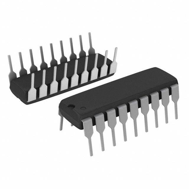
| 描述 | IC SUPPLY/LINE MONITOR 18-DIP监控电路 Quad Supply and Line Monitor |
| 产品分类 | |
| 品牌 | Texas Instruments |
| 产品手册 | |
| 产品图片 |
|
| rohs | 符合RoHS无铅 / 符合限制有害物质指令(RoHS)规范要求 |
| 产品系列 | 电源管理 IC,监控电路,Texas Instruments UC2903N- |
| NumberofInputsMonitored | 4 Input |
| 数据手册 | |
| 产品型号 | UC2903N |
| 产品目录页面 | |
| 产品种类 | 监控电路 |
| 人工复位 | No Manual Reset |
| 供应商器件封装 | 18-PDIP |
| 其它名称 | 296-11207-5 |
| 包装 | 管件 |
| 单位重量 | 1.206 g |
| 受监控电压数 | 4 |
| 商标 | Texas Instruments |
| 复位 | 低有效 |
| 复位超时 | 可调节/可选择 |
| 安装类型 | 通孔 |
| 安装风格 | Through Hole |
| 封装 | Tube |
| 封装/外壳 | 18-DIP(0.300",7.62mm) |
| 封装/箱体 | PDIP-18 |
| 工作温度 | -40°C ~ 85°C |
| 工作电源电流 | 7000 uA |
| 工厂包装数量 | 20 |
| 最大功率耗散 | 1000 mW |
| 最大工作温度 | + 85 C |
| 最小工作温度 | - 40 C |
| 标准包装 | 20 |
| 欠电压阈值 | Adjustable |
| 电压-阈值 | 可调节/可选择 |
| 电池备用开关 | No Backup |
| 电源电压-最大 | 40 V |
| 电源电压-最小 | 8 V |
| 监视器 | No Watchdog |
| 类型 | 多压监控器 |
| 系列 | UC2903 |
| 被监测输入数 | 4 Input |
| 输出 | 推挽式,图腾柱 |
| 输出类型 | Open Collector / Drain |
| 过电压阈值 | Adjustable |
| 重置延迟时间 | Adjustable |
| 阈值电压 | Adjustable |


- 商务部:美国ITC正式对集成电路等产品启动337调查
- 曝三星4nm工艺存在良率问题 高通将骁龙8 Gen1或转产台积电
- 太阳诱电将投资9.5亿元在常州建新厂生产MLCC 预计2023年完工
- 英特尔发布欧洲新工厂建设计划 深化IDM 2.0 战略
- 台积电先进制程称霸业界 有大客户加持明年业绩稳了
- 达到5530亿美元!SIA预计今年全球半导体销售额将创下新高
- 英特尔拟将自动驾驶子公司Mobileye上市 估值或超500亿美元
- 三星加码芯片和SET,合并消费电子和移动部门,撤换高东真等 CEO
- 三星电子宣布重大人事变动 还合并消费电子和移动部门
- 海关总署:前11个月进口集成电路产品价值2.52万亿元 增长14.8%


PDF Datasheet 数据手册内容提取
UC1903 UC2903 UC3903 www.ti.com........................................................................................................................................ SLUS233A–OCTOBER1999–REVISEDSEPTEMBER2008 Quad Supply and Line Monitor FEATURES DESCRIPTION 1 • InputsforMonitoringuptoFourSeparate The UC1903 family of quad supply and line monitor SupplyVoltageLevels integrated circuits will respond to under- and • InternalInverterforSensingaNegativeSupply over-voltage conditions on up to four continuously Voltage monitored voltage levels. An internal op-amp inverter allows at least one of these levels to be negative. A • Line/SwitchSenseInputforEarlyPower separate line/switcher sense input is available to SourceFailureWarning provide early warning of line or other power source • ProgrammableUnder-andOver-VoltageFault failures. ThresholdswithProportionalHysteresis The fault window adjustment circuit on these devices • APrecision2.5-VReference provides easy programming of under- and • GeneralPurposeOp-AmpforAuxiliaryUse over-voltage thresholds. The thresholds, centered • ThreeHighCurrent,>30mA,Open-Collector around a precision 2.5-V reference, have an input hysteresis that scales with the window width for OutputsIndicateOver-Voltage,Under-Voltage precise, glitch-free operation. A reference output pin andPowerOKConditions allows the sense input fault windows to be scaled • 8-Vto40-VSupplyOperationwith7-mA independentlyusingsimpleresistivedividers. Stand-ByCurrent The three open collector outputs on these devices sink in excess of 30 mA of load current when active. The under- and over-voltage outputs respond after separate, user defined, delays to respective fault conditions. The third output is active during any fault condition including under- and over-voltage, line/switcher faults, and input supply under-voltage. The off state of this output indicates a "power OK" situation. BLOCK DIAGRAM Note:PinnumbersrefertoJ,NandDWpackages. 1 Pleasebeawarethatanimportantnoticeconcerningavailability,standardwarranty,anduseincriticalapplicationsofTexas Instrumentssemiconductorproductsanddisclaimerstheretoappearsattheendofthisdatasheet. PRODUCTIONDATAinformationiscurrentasofpublicationdate. Copyright©1999–2008,TexasInstrumentsIncorporated Products conform to specifications per the terms of the Texas Instruments standard warranty. Production processing does not necessarilyincludetestingofallparameters.
UC1903 UC2903 UC3903 SLUS233A–OCTOBER1999–REVISEDSEPTEMBER2008........................................................................................................................................ www.ti.com DESCRIPTION (CONT.) An additional, uncommitted, general purpose op-amp is also included. This op-amp, capable of sourcing 20 mA of output current, can be used for a number of auxiliary functions including the sensing and amplification of a feedbackerrorsignalwhenthe2.5-Voutputisusedasasystemreference. Thesepartsoperateoveran8-Vto40-Vinputsupplyrangeandrequireatypicalstand-bycurrentofonly7mA. CONNECTION DIAGRAMS DIL-18, SOIC-18 PLCC-20, LCC-20 J or N, DW PACKAGE Q, LPACKAGE (TOPVIEW) (TOPVIEW) +VIN 1 18 G.P. OP-AMPINV. INV N.I. P P V (2.5 V) 2 17 G.P. OP-AMPN.I. M M REF V) A A GND 3 16 G.P. OP-AMPOUT 5 P- P- 2. O O WINDOWSAEDNJSUES T4 45 1154 LPIONWE/ESRW OITKCHER SENSE GND V(REF +VIN G.P. G.P. INVERTINPUT SENSE 4 6 13 UV DELAY 3 2 1 20 19 SENSE 3 7 12 UV FAULT GND 4 18 G.P. OP-AMPOUT SENSE 2 8 11 OV FAULT WINDOWADJUST 5 17 LINE/SWITCHER SENSE SENSE 1 9 10 OV DELAY NC 6 16 POWER OK SENSE 4 INVERT 7 15 UV DELAY INPUT SENSE 4 8 14 UV FAULT 9 10 11 12 13 E 3 E 2 E 1 AY LT S S S L U N N N E A SE SE SE V D V F O O ABSOLUTE MAXIMUM RATINGS(1) overoperatingfree-airtemperaturerange(unlessotherwisenoted) VALUE UNIT +VIN SupplyVoltage +40 V OpenCollectorOutputVoltages. +40 V OpenCollectorOutputCurrents. 50 mA Sense1-4InputVoltages –0.3to+20 V Line/SwitcherSenseInputVoltage –0.3to+40 V Op-AmpandInverterInputVoltages –0.3to+40 V Op-AmpandInverterOutputCurrents. –40 mA WindowAdjustVoltage. 0.0to+10 V DelayPinVoltages 0.0to+5 V ReferenceOutputCurrent –40 mA PowerDissipationatT =25°C(1) 1000 mW A PowerDissipationatT =25°C(1) 2000 mW C OperatingJunctionTemperature –55to+150 °C StorageTemperature –65to+150 C LeadTemperature(Soldering,10Seconds) 300 °C (1) Voltagesarereferencedtoground(Pin3).Currentsarepositiveinto,negativeoutof,thespecifiedterminals.ConsultPackagingSection ofDatabookforthermallimitationsandconsiderationsofpackage. 2 SubmitDocumentationFeedback Copyright©1999–2008,TexasInstrumentsIncorporated ProductFolderLink(s):UC1903UC2903UC3903
UC1903 UC2903 UC3903 www.ti.com........................................................................................................................................ SLUS233A–OCTOBER1999–REVISEDSEPTEMBER2008 ELECTRICAL CHARACTERISTICS Unlessotherwisestated,thesespecificationsapplyforT =–55°Cto+125°CfortheUC1903;–40°Cto+85°Cforthe A UC2903;and0°Cto+70°CfortheUC3903;+V =15V;SenseInputs(Pins6–9andPin15)=2.5V;V 4=1.0V,T =T. IN PIN A J UC1903/UC2903 UC3903 PARAMETER TESTCONDITIONS UNIT MIN TYP MAX MIN TYP MAX SUPPLY InputSupplyCurrent NoFaults 7 9 7 11 mA UV,OVandLineFault 10 15 10 18 mA SupplyUnderVoltageThreshold FaultOutputsEnabled 6.0 7.0 7.5 5.5 7.0 8.0 V (VSUV) MinimumSupplytoEnablePower 3.0 4.0 3.0 4.0 V OKOutput REFERENCE OutputVoltage(VREF) TJ=25°C 2.485 2.5 2.515 2.470 2.5 2.530 V OverTemperature 2.465 2.535 2.465 2.535 V LoadRegulation IL=0to10mA 1 10 1 15 mV LineRegulation +VIN=8to40V 1 4 1 8 mV ShortCircuitCurrent TJ=25°C 40 40 mA FAULTTHRESHOLDS(1) OVThresholdAdj. OffsetfromVREFasafunctionofVPIN 0.230 0.25 0.270 0.230 0.25 0.270 V/V 4Input=LowtoHigh,0.5V≤VPIN4≤2.5V UVThresholdAdj. OffsetfromVREFasafunctionofVPIN –0.270 –0.25 –0.230 –0.270 –0.25 –0.270 V/V 4Input=HightoLow,0.5V≤VPIN4≤2.5V OV&UVThresholdHyst. 0.5V≤VPIN4≤2.5V 10 20 30 10 20 30 mV/V OV&UVThresholdSupply +VIN=8Vto40V 0.002 0.01 0.002 0.02 %/V Sensitivity AdjustPin(Pin4)InputBiasCurrent 0.5V≤VPIN4≤2.5V ±1 ±10 ±1 ±12 m A/V LineSenseThreshold Input=HightoLow 1.94 2.0 2.06 1.9 2.0 2.1 V LineSenseThresholdHyst. 125 175 225 100 175 250 mV SENSEINPUTS Input=2.8V(2) 1 3 1 6 m A Sense1-4InputBiasCurrent Input=2.2(2) –1 –3 –1 -6 m A LineSenseInputBiasCurrent Input=2.3V(2) 1 3 1 6 m A OVANDUVFAULTDELAY ChargingCurrent 60 60 m A ThresholdVoltage DelayPin=LowtoHigh 1.8 1.8 V ThresholdHysteresis TJ=25°C 250 250 mV Delay RatioofThresholdVoltagetoCharging 20 30 50 20 30 50 ms/m F Current (1) Referencetopinnumbersinthisspecificationpertainto18pinDILNandJpackagesand18pinSOICDWpackage. (2) Thesecurrentsrepresentmaximuminputbiascurrentsrequiredasthesenseinputscrossappropriatethresholds. Copyright©1999–2008,TexasInstrumentsIncorporated SubmitDocumentationFeedback 3 ProductFolderLink(s):UC1903UC2903UC3903
UC1903 UC2903 UC3903 SLUS233A–OCTOBER1999–REVISEDSEPTEMBER2008........................................................................................................................................ www.ti.com ELECTRICAL CHARACTERISTICS (continued) Unlessotherwisestated,thesespecificationsapplyforT =–55°Cto+125°CfortheUC1903;–40°Cto+85°Cforthe A UC2903;and0°Cto+70°CfortheUC3903;+V =15V;SenseInputs(Pins6–9andPin15)=2.5V;V 4=1.0V,T =T. IN PIN A J UC1903/UC2903 UC3903 PARAMETER TESTCONDITIONS UNIT MIN TYP MAX MIN TYP MAX FAULTOUTPUTS(OV,UV,ANDPOWER0K) MaximumCurrent VOUT=2V 30 70 30 70 mA SaturationVoltage IOUT=12mA 0.25 0.40 0.25 0.40 V LeakageCurrent VOUT=40V 3 25 3 25 m A SENSE4INVERTER(3) InputOffsetVoltage 2 8 2 10 mV InputBiasCurrent 0.1 2 0.1 4 m A OpenLoopGain 65 80 65 80 dB PSRR +VIN=8to40V 65 100 65 100 dB UnityGainFrequency 1 1 MHz SlewRate 0.4 0.4 V/m s ShortCircuitCurrent TJ=2°C 40 40 mA G.P.OP-AMP(3) InputOffsetVoltage 1 5 1 8 mV InputBiasVoltage 0.1 2 0.1 4 m A InputOffsetCurrent 0.01 .5 0.01 1.0 m A OpenLoopGain 65 120 65 120 dB CMRR VCM=0to+VIN=2.0V 65 100 65 100 dB PSRR +VIN=8to40V 65 100 65 100 dB UnityGainFrequency 1 1 MHz SlewRate 0.4 0.4 V/m s ShortCircuitCurrent TJ=25°C 40 40 mA (3) WheneithertheG.P.OP-Amp,ortheSense4Inverter,areconfiguredforsensinganegativesupplyvoltage,thedividerresistanceat theinvertinginputshouldbechosensuchthatthenominaldividercurrentis≤1.4mA.Withthedividercurrentatorbelowthislevel possiblelatchingofthecircuitisavoided.Properoperationforcurrentsatorbelow1.4mAis100%testedinproduction. 4 SubmitDocumentationFeedback Copyright©1999–2008,TexasInstrumentsIncorporated ProductFolderLink(s):UC1903UC2903UC3903
UC1903 UC2903 UC3903 www.ti.com........................................................................................................................................ SLUS233A–OCTOBER1999–REVISEDSEPTEMBER2008 BlockDiagram UC1903 +VIN TO REFERENCE I I OA OB Q4 OV HYSTERESIS CIRCUIT CONTROL 1.25 V Q2 Q1 OV THRESHOLD Q3 R5 1.84 kW 2.5 V 15W R1 OUTPUT R6 0.16 kW FAULT WINDOW 2.5 kW R2 THREAHOLD and HYSTERESIS CIRCUITS 0.16 kW R7 2.5 kW R3 R8 1.84 kW RA IO = VRA4DJ UV THRESHOLD R4 VADJ RS BIAS 8 kW IOC IOD Q5 TUOV HYSTERESIS CANCELLATION CONTROL AND MIRROR CIRCUITS A. The UC1903 fault window circuitry generates OV and UV thresholds centered around the 2.5-V reference. Window magnitudeandthresholdhysteresisareproportionaltothewindowadjustinputvoltageatPin4. Figure1.OperationandApplicationInformation Typical Characteristics Typical 2.5 V Reference Typical Fault Delay vs vs Temperature Characteristic Temperature Characteristic (C ≥270 pF) DELAY 0.2 0.1 40 0 % e - - 0.1 35 g an - 0.2 mF h s/ C m rence - 0.3 elay - 30 efe - 0.4 D R - 0.5 25 - 0.6 - 0.7 - 55 - 35 - 15 5 25 45 65 85 105 125 20 T - Junction Temperature - °C - 55 - 35 - 15 5 25 45 65 85 105 125 J T - Junction Temperature - °C J Copyright©1999–2008,TexasInstrumentsIncorporated SubmitDocumentationFeedback 5 ProductFolderLink(s):UC1903UC2903UC3903
UC1903 UC2903 UC3903 SLUS233A–OCTOBER1999–REVISEDSEPTEMBER2008........................................................................................................................................ www.ti.com OPERATION AND APPLICATION INFORMATION Setting a Fault Window The fault thresholds on the UC1903 are generated by creating positive and negative offsets, equal in magnitude, that are referenced to the chip’s 2.5-V reference. The resulting fault window is centered around 2.5 V and has a magnitude equal to that of the applied offsets. Simplified schematics of the fault window and reference circuits are shown in Figure 1 along with the Typical Characteristics diagrams. The magnitude of the offsets is determined by the voltage applied at the window adjust pin, Pin 4. A bias cancellation circuit keeps the input current required at Pin 4 low, allowing the use of a simple resistive divider off the reference to set the adjust pin voltage. The adjust voltage at Pin 4 is internally applied across R4, and an 8-kΩ resistor. The resulting current is mirrored four times to generate current sources I , I , I , and I , all equal in magnitude. When all four of the sense OA OB OC OD inputs are inside the fault window, a no-fault condition, Q4 and Q5 are turned on. In combination with D1 and D2 this prevents L and L from affecting the fault thresholds. In this case, the OV and UV thresholds are equal to OB OD V +I (R5+R6)andV –I (R7+R8)respectively.Thefaultwindowcanbeexpressedas: REF OA REF OC V 2.5 V ± ADJ 4 (1) Intermsofasensednominalvoltagelevel,V ,thewindowasapercentvariationis: S ( ) V ± 10 × V % S ADJ (2) WhenasenseinputmovesoutsidethefaultwindowgiveninEquation1,theappropriatehysteresiscontrolsignal turns off Q4 or Q5. For the under-voltage case, Q5 is disabled and current source I flows through D2. The net OB current through R7 becomes zero as I cancels I , giving an 8% reduction in the UV threshold offset. The OB OC overvoltage case is the same, with Q4 turning off, allowing I to cancel the current flow, I , through R6. The OD OA result is a hysteresis at the sense inputs which is always 8% of the window magnitude. This is shown graphically inFigure2. 3.125 25 3 20 V s - 2.875 15 % nput 2.750 Hysteresis 10 w - se I 2.625 5 ndo n Wi e Fault ow at S 2.327.55 Window 0-5 y Fault Wind 2.25 -10 uppl ult 2.125 No Fault -15 S a F Fault 2 -20 Fault Window 1.875 -25 0 0.5 1 1.5 2 2.5 WindowAdjust Voltage (V ) at Pin 4 ADJ Figure2.FaultWindowandThresholdHysteresisScaleasaFunctionoftheVoltageAppliedatPin4 6 SubmitDocumentationFeedback Copyright©1999–2008,TexasInstrumentsIncorporated ProductFolderLink(s):UC1903UC2903UC3903
UC1903 UC2903 UC3903 www.ti.com........................................................................................................................................ SLUS233A–OCTOBER1999–REVISEDSEPTEMBER2008 Fault Windows Scaled Independently In many applications, it may be desirable to monitor various supply voltages, or voltage levels, with varying fault windows. Using the reference output and external resistive dividers this is easily accomplished with the UC1903. Figure 3 and Figure 4 illustrate how the fault window at any sense input can be scaled independently of the remaininginputs. Monitored Supply Voltage V S UC1903 R1 SENSE 1-4 INPUT R3 R2 2.5 V REF. FaultwindowfortheSenseInput, inpercent,is: R3+R1R2/(R1+R2) –10(VADJ)• , R3 for: R2 VS(NOM)• = 2.5V R1+R2 A. Using the reference output and a resistive divider, a sense input with an independently wider fault window can be generated. Figure3.UC1903SenseInputwithanIndependentlyWiderFaultWindow UC1903 G.P. OP-AMP R1 SENSE INPUT R2 2.5 V REF. SENSE 1-4 INPUT Faultwindowforthesenseinput,inpercent,is: R2 ±10 (V ) • ADJ R1+R2 A. Thegeneralpurposeop-ampontheUC1903canbeusedtocreateasenseinputwithanindependentlytighterfault window. Figure4.UC1903SenseInputwithanIndependentlyTighterFaultWindow Copyright©1999–2008,TexasInstrumentsIncorporated SubmitDocumentationFeedback 7 ProductFolderLink(s):UC1903UC2903UC3903
UC1903 UC2903 UC3903 SLUS233A–OCTOBER1999–REVISEDSEPTEMBER2008........................................................................................................................................ www.ti.com Figure4demonstratesoneofmanyauxiliaryfunctionsthattheuncommittedop-ampontheUC1903canbeused for. Alternatively, this op-amp can be used to buffer high impedance points, perform logic functions, or for sensing and amplification. For example, the G.P. op-amp, combined with the 2.5-V reference, can be used to produce and buffer an optically coupled feedback signal in isolated supplies with primary side control. The output stage of this op-amp is detailed in Figure 5. The NPN emitter follower provides high source current capability. ≥20mAwhilethesubstratedevice,Q3,providesgoodtransientsinkingcapability. +V IN 75mA Q1 Q2 R1 10 kW UC1903 G.P. OP-AMPD1 Q6 R2 OUTPUT STAGE 15W 16 R3 OUTPUT 150W Q3 TO OP-AMP Q5 INPUT STAGE Q4 R4 500W 150mA A. The G.P. op-amp on the UC1903 has a high source current (20 mA) capability and enhanced transient sinking capabilitythroughsubstratedeviceQ3. Figure5.TheG.P.Op-AmpontheUC1903 Sensing a Negative Voltage Level The UC1903 has a dedicated inverter coupled to the sense 4 input. With this inverter, a negative voltage level can be sensed as shown in Figure 6. The output of the inverter is an unbiased emitter follower. By tying the inverting input, Pin 5, high the output emitter follower will be reverse biased, leaving the sense 4 input in a high impedance state. In this manner, the sense 4 input can be used, as the remaining sense inputs would be, for sensingpositivevoltagelevels. UC1903 SENSE 4 INPUT 2.5 V R1 SENSE 4 VS R2 INVERTER GROUND NEGATIVE V (NOM) = 2.5 V SUPPLY(-V ) S S Note:Asimilarschemew/theG.P.op-ampwillallowasec- ondnegativesupplytobemonitored. Figure6.InvertingtheSense4InputforMonitoringaNegativeSupply,Accommodatedwiththe DedicatedInverter 8 SubmitDocumentationFeedback Copyright©1999–2008,TexasInstrumentsIncorporated ProductFolderLink(s):UC1903UC2903UC3903
UC1903 UC2903 UC3903 www.ti.com........................................................................................................................................ SLUS233A–OCTOBER1999–REVISEDSEPTEMBER2008 Using The Line/Switcher Sense Output The line switcher sense input to the UC1903 can be used for early detection of line, switcher, or other power source, failures. Internally referenced to 2.0 V, the line sense comparator will cause the POWER OK output to indicate a fault (active low) condition when the LINE/SWITCHER SENSE input goes from above to below 2.0 V. The line sense comparator has approximately 175 mV of hysteresis requiring the line/switcher input to reach 2.175 V before the POWER OK output device can be turned off, allowing a no-fault indication. In Figure 7 an example showing the use of the LINE/SWITCHER SENSE input for early switcher-fault detection is detailed. A sample signal is taken from the output of the power transformer, rectified and filtered, and used at the line/switcher input. By adjusting the R C time constant with respect to the switching frequency of the supply and 2 the hold up time of the output capacitor, switcher faults can be detected before supply outputs are significantly affected. LINE POWER INPUT TRANSFORMER FILTER Figure7.Line/SwitcherSenseInputUsedforEarlyLineorSwitcherFaultIndication Copyright©1999–2008,TexasInstrumentsIncorporated SubmitDocumentationFeedback 9 ProductFolderLink(s):UC1903UC2903UC3903
UC1903 UC2903 UC3903 SLUS233A–OCTOBER1999–REVISEDSEPTEMBER2008........................................................................................................................................ www.ti.com OV and UV Comparators Maintain Accurate Thresholds The structure of the OV and UV comparators, shown in Figure 8 results in accurate fault thresholds even in the case where multiple sense inputs cross a fault threshold simultaneously. Unused sense inputs can be tied either to the 2.5-V reference, or to another, utilized, sense input. The four under- and over-voltage sense inputs on the UC1903areclampedasdetailed on the Sense 1 input in Figure 8. The series 2-kΩ resistor, R1, and zener diode Z1, prevent extreme under- and over-voltage conditions from inverting the outputs of the fault comparators. A parasitic diode, D1, is present at the inputs as well. Under normal operation it is advisable to insure that voltage levels at all of the sense inputs stay above –0.3 V. The same type of input protection exists at the line sense input,Pin15,excepta5-kΩseriesresistorisused. The fault delay circuitry on the UC1903 is also shown in Figure 8. In the case of an over-voltage condition at one of the sense inputs Q20 is turned off, allowing the internal 60-mA current source to charge the user-selected delay capacitor. When the capacitor voltage reaches 1.8 V, the OV and POWER OK outputs become active low. When the fault condition goes away Q20 is turned back on, rapidly discharging the delay capacitor. Operation of theunder-voltagedelayis,withappropriatesubstitutions,thesame. 6.4 V EXT. 6.4 V OV DELAY 60mA CAPACITOR Q6 Q7 Q8 Q9 OV FAULT INDICATION Q20 TO OUTPUT OV COMPARATOR 1.8 V LOGIC Q1 Q2 Q3 Q4 Q5 OV SENSE 1 TO OV HYSTERESIS 2 kW THRESHOLD CONTROL 100mA VOLTAGE R1 D1 Z1 5.7 V SENSE 2 6.4 V 50mA SENSE 3 TO UV SENSE 4 THVROELSTAHGOELDHYSTUEVRESIS 6.4 V VREF EXT. Q10 Q11 Q12 Q13 Q14 CONTROL 60mA UV DELAY CAPACITOR UV FAULT UV COMPARATOR INDICATION Q19 TO OUTPUT 1.8 V Q15 Q16 Q17 Q18 LOGIC A. The OV and UV comparators on the UC1903 trigger respective fault delay circuits when one or more of the sense inputs move outside the fault window. Input clamps insure proper operation under extreme fault conditions. TerminatingtheUVdelaycapacitortoVREFassurescorrectlogicatpowerup. Figure8.OVandUVComparatorsontheUC1903 Start Latch and Supply Under-Voltage Sense Allow Predictable Power-Up At power-Up, while the +V input supply is below 3 V, all open collector outputs are off. With +V greater than 3 IN IN V the POWER OK output will be driven low and the UV OV FAULT outputs are disabled. Once +V rises above IN the V threshold of 7 V the fault outputs will be enabled. As would be expected, the SENSE 1-4 voltages at SUV powerupmaybebelowtheUVFAULTwindowandtheUVFAULToutputmaybedrivenlow. 10 SubmitDocumentationFeedback Copyright©1999–2008,TexasInstrumentsIncorporated ProductFolderLink(s):UC1903UC2903UC3903
PACKAGE OPTION ADDENDUM www.ti.com 11-Jul-2015 PACKAGING INFORMATION Orderable Device Status Package Type Package Pins Package Eco Plan Lead/Ball Finish MSL Peak Temp Op Temp (°C) Device Marking Samples (1) Drawing Qty (2) (6) (3) (4/5) 5962-88697012A ACTIVE LCCC FK 20 1 TBD POST-PLATE N / A for Pkg Type -55 to 125 5962- 88697012A UC1903L/ 883B 5962-8869701VA ACTIVE CDIP J 18 1 TBD A42 N / A for Pkg Type -55 to 125 5962-8869701VA UC1903J/883B UC1903J ACTIVE CDIP J 18 1 TBD A42 N / A for Pkg Type -55 to 125 UC1903J UC1903J883B ACTIVE CDIP J 18 1 TBD A42 N / A for Pkg Type -55 to 125 5962-8869701VA UC1903J/883B UC1903L ACTIVE LCCC FK 20 1 TBD POST-PLATE N / A for Pkg Type -55 to 125 UC1903L UC1903L883B ACTIVE LCCC FK 20 1 TBD POST-PLATE N / A for Pkg Type -55 to 125 5962- 88697012A UC1903L/ 883B UC2903DW ACTIVE SOIC DW 18 40 Green (RoHS CU NIPDAU Level-2-260C-1 YEAR -40 to 85 UC2903DW & no Sb/Br) UC2903DWG4 ACTIVE SOIC DW 18 40 Green (RoHS CU NIPDAU Level-2-260C-1 YEAR -40 to 85 UC2903DW & no Sb/Br) UC2903DWTR ACTIVE SOIC DW 18 2000 Green (RoHS CU NIPDAU Level-2-260C-1 YEAR -40 to 85 UC2903DW & no Sb/Br) UC2903DWTRG4 ACTIVE SOIC DW 18 2000 Green (RoHS CU NIPDAU Level-2-260C-1 YEAR -40 to 85 UC2903DW & no Sb/Br) UC2903J LIFEBUY CDIP J 18 1 TBD A42 N / A for Pkg Type -40 to 85 UC2903J UC2903N LIFEBUY PDIP N 18 20 Green (RoHS CU NIPDAU N / A for Pkg Type -40 to 85 UC2903N & no Sb/Br) UC2903NG4 ACTIVE PDIP N 18 TBD Call TI Call TI -40 to 85 UC2903Q ACTIVE PLCC FN 20 46 Green (RoHS CU SN Level-2-260C-1 YEAR -40 to 85 UC2903Q & no Sb/Br) UC3903DW ACTIVE SOIC DW 18 40 Green (RoHS CU NIPDAU Level-2-260C-1 YEAR 0 to 70 UC3903DW & no Sb/Br) UC3903DWG4 ACTIVE SOIC DW 18 TBD Call TI Call TI 0 to 70 Addendum-Page 1
PACKAGE OPTION ADDENDUM www.ti.com 11-Jul-2015 Orderable Device Status Package Type Package Pins Package Eco Plan Lead/Ball Finish MSL Peak Temp Op Temp (°C) Device Marking Samples (1) Drawing Qty (2) (6) (3) (4/5) UC3903DWTR ACTIVE SOIC DW 18 2000 Green (RoHS CU NIPDAU Level-2-260C-1 YEAR 0 to 70 UC3903DW & no Sb/Br) UC3903DWTRG4 ACTIVE SOIC DW 18 2000 Green (RoHS CU NIPDAU Level-2-260C-1 YEAR 0 to 70 UC3903DW & no Sb/Br) UC3903J LIFEBUY CDIP J 18 1 TBD A42 N / A for Pkg Type 0 to 70 UC3903J UC3903N LIFEBUY PDIP N 18 20 Green (RoHS CU NIPDAU N / A for Pkg Type 0 to 70 UC3903N & no Sb/Br) UC3903NG4 LIFEBUY PDIP N 18 20 Green (RoHS CU NIPDAU N / A for Pkg Type 0 to 70 UC3903N & no Sb/Br) UC3903Q ACTIVE PLCC FN 20 46 Green (RoHS CU SN Level-2-260C-1 YEAR 0 to 70 UC3903Q & no Sb/Br) UC3903QG3 ACTIVE PLCC FN 20 46 Green (RoHS CU SN Level-2-260C-1 YEAR 0 to 70 UC3903Q & no Sb/Br) (1) The marketing status values are defined as follows: ACTIVE: Product device recommended for new designs. LIFEBUY: TI has announced that the device will be discontinued, and a lifetime-buy period is in effect. NRND: Not recommended for new designs. Device is in production to support existing customers, but TI does not recommend using this part in a new design. PREVIEW: Device has been announced but is not in production. Samples may or may not be available. OBSOLETE: TI has discontinued the production of the device. (2) Eco Plan - The planned eco-friendly classification: Pb-Free (RoHS), Pb-Free (RoHS Exempt), or Green (RoHS & no Sb/Br) - please check http://www.ti.com/productcontent for the latest availability information and additional product content details. TBD: The Pb-Free/Green conversion plan has not been defined. Pb-Free (RoHS): TI's terms "Lead-Free" or "Pb-Free" mean semiconductor products that are compatible with the current RoHS requirements for all 6 substances, including the requirement that lead not exceed 0.1% by weight in homogeneous materials. Where designed to be soldered at high temperatures, TI Pb-Free products are suitable for use in specified lead-free processes. Pb-Free (RoHS Exempt): This component has a RoHS exemption for either 1) lead-based flip-chip solder bumps used between the die and package, or 2) lead-based die adhesive used between the die and leadframe. The component is otherwise considered Pb-Free (RoHS compatible) as defined above. Green (RoHS & no Sb/Br): TI defines "Green" to mean Pb-Free (RoHS compatible), and free of Bromine (Br) and Antimony (Sb) based flame retardants (Br or Sb do not exceed 0.1% by weight in homogeneous material) (3) MSL, Peak Temp. - The Moisture Sensitivity Level rating according to the JEDEC industry standard classifications, and peak solder temperature. (4) There may be additional marking, which relates to the logo, the lot trace code information, or the environmental category on the device. (5) Multiple Device Markings will be inside parentheses. Only one Device Marking contained in parentheses and separated by a "~" will appear on a device. If a line is indented then it is a continuation of the previous line and the two combined represent the entire Device Marking for that device. Addendum-Page 2
PACKAGE OPTION ADDENDUM www.ti.com 11-Jul-2015 (6) Lead/Ball Finish - Orderable Devices may have multiple material finish options. Finish options are separated by a vertical ruled line. Lead/Ball Finish values may wrap to two lines if the finish value exceeds the maximum column width. Important Information and Disclaimer:The information provided on this page represents TI's knowledge and belief as of the date that it is provided. TI bases its knowledge and belief on information provided by third parties, and makes no representation or warranty as to the accuracy of such information. Efforts are underway to better integrate information from third parties. TI has taken and continues to take reasonable steps to provide representative and accurate information but may not have conducted destructive testing or chemical analysis on incoming materials and chemicals. TI and TI suppliers consider certain information to be proprietary, and thus CAS numbers and other limited information may not be available for release. In no event shall TI's liability arising out of such information exceed the total purchase price of the TI part(s) at issue in this document sold by TI to Customer on an annual basis. OTHER QUALIFIED VERSIONS OF UC1903, UC2903, UC2903M, UC3903, UC3903M : •Catalog: UC3903, UC2903, UC3903M, UC3903 •Military: UC2903M, UC1903, UC1903 NOTE: Qualified Version Definitions: •Catalog - TI's standard catalog product •Military - QML certified for Military and Defense Applications Addendum-Page 3
PACKAGE MATERIALS INFORMATION www.ti.com 11-Mar-2014 TAPE AND REEL INFORMATION *Alldimensionsarenominal Device Package Package Pins SPQ Reel Reel A0 B0 K0 P1 W Pin1 Type Drawing Diameter Width (mm) (mm) (mm) (mm) (mm) Quadrant (mm) W1(mm) UC2903DWTR SOIC DW 18 2000 330.0 24.4 10.9 12.0 2.7 12.0 24.0 Q1 UC3903DWTR SOIC DW 18 2000 330.0 24.4 10.9 12.0 2.7 12.0 24.0 Q1 PackMaterials-Page1
PACKAGE MATERIALS INFORMATION www.ti.com 11-Mar-2014 *Alldimensionsarenominal Device PackageType PackageDrawing Pins SPQ Length(mm) Width(mm) Height(mm) UC2903DWTR SOIC DW 18 2000 367.0 367.0 45.0 UC3903DWTR SOIC DW 18 2000 367.0 367.0 45.0 PackMaterials-Page2
IMPORTANTNOTICE TexasInstrumentsIncorporatedanditssubsidiaries(TI)reservetherighttomakecorrections,enhancements,improvementsandother changestoitssemiconductorproductsandservicesperJESD46,latestissue,andtodiscontinueanyproductorserviceperJESD48,latest issue.Buyersshouldobtainthelatestrelevantinformationbeforeplacingordersandshouldverifythatsuchinformationiscurrentand complete.Allsemiconductorproducts(alsoreferredtohereinas“components”)aresoldsubjecttoTI’stermsandconditionsofsale suppliedatthetimeoforderacknowledgment. TIwarrantsperformanceofitscomponentstothespecificationsapplicableatthetimeofsale,inaccordancewiththewarrantyinTI’sterms andconditionsofsaleofsemiconductorproducts.TestingandotherqualitycontroltechniquesareusedtotheextentTIdeemsnecessary tosupportthiswarranty.Exceptwheremandatedbyapplicablelaw,testingofallparametersofeachcomponentisnotnecessarily performed. TIassumesnoliabilityforapplicationsassistanceorthedesignofBuyers’products.Buyersareresponsiblefortheirproductsand applicationsusingTIcomponents.TominimizetherisksassociatedwithBuyers’productsandapplications,Buyersshouldprovide adequatedesignandoperatingsafeguards. TIdoesnotwarrantorrepresentthatanylicense,eitherexpressorimplied,isgrantedunderanypatentright,copyright,maskworkright,or otherintellectualpropertyrightrelatingtoanycombination,machine,orprocessinwhichTIcomponentsorservicesareused.Information publishedbyTIregardingthird-partyproductsorservicesdoesnotconstitutealicensetousesuchproductsorservicesorawarrantyor endorsementthereof.Useofsuchinformationmayrequirealicensefromathirdpartyunderthepatentsorotherintellectualpropertyofthe thirdparty,oralicensefromTIunderthepatentsorotherintellectualpropertyofTI. ReproductionofsignificantportionsofTIinformationinTIdatabooksordatasheetsispermissibleonlyifreproductioniswithoutalteration andisaccompaniedbyallassociatedwarranties,conditions,limitations,andnotices.TIisnotresponsibleorliableforsuchaltered documentation.Informationofthirdpartiesmaybesubjecttoadditionalrestrictions. ResaleofTIcomponentsorserviceswithstatementsdifferentfromorbeyondtheparametersstatedbyTIforthatcomponentorservice voidsallexpressandanyimpliedwarrantiesfortheassociatedTIcomponentorserviceandisanunfairanddeceptivebusinesspractice. TIisnotresponsibleorliableforanysuchstatements. Buyeracknowledgesandagreesthatitissolelyresponsibleforcompliancewithalllegal,regulatoryandsafety-relatedrequirements concerningitsproducts,andanyuseofTIcomponentsinitsapplications,notwithstandinganyapplications-relatedinformationorsupport thatmaybeprovidedbyTI.Buyerrepresentsandagreesthatithasallthenecessaryexpertisetocreateandimplementsafeguardswhich anticipatedangerousconsequencesoffailures,monitorfailuresandtheirconsequences,lessenthelikelihoodoffailuresthatmightcause harmandtakeappropriateremedialactions.BuyerwillfullyindemnifyTIanditsrepresentativesagainstanydamagesarisingoutoftheuse ofanyTIcomponentsinsafety-criticalapplications. Insomecases,TIcomponentsmaybepromotedspecificallytofacilitatesafety-relatedapplications.Withsuchcomponents,TI’sgoalisto helpenablecustomerstodesignandcreatetheirownend-productsolutionsthatmeetapplicablefunctionalsafetystandardsand requirements.Nonetheless,suchcomponentsaresubjecttotheseterms. NoTIcomponentsareauthorizedforuseinFDAClassIII(orsimilarlife-criticalmedicalequipment)unlessauthorizedofficersoftheparties haveexecutedaspecialagreementspecificallygoverningsuchuse. OnlythoseTIcomponentswhichTIhasspecificallydesignatedasmilitarygradeor“enhancedplastic”aredesignedandintendedforusein military/aerospaceapplicationsorenvironments.BuyeracknowledgesandagreesthatanymilitaryoraerospaceuseofTIcomponents whichhavenotbeensodesignatedissolelyattheBuyer'srisk,andthatBuyerissolelyresponsibleforcompliancewithalllegaland regulatoryrequirementsinconnectionwithsuchuse. TIhasspecificallydesignatedcertaincomponentsasmeetingISO/TS16949requirements,mainlyforautomotiveuse.Inanycaseofuseof non-designatedproducts,TIwillnotberesponsibleforanyfailuretomeetISO/TS16949. Products Applications Audio www.ti.com/audio AutomotiveandTransportation www.ti.com/automotive Amplifiers amplifier.ti.com CommunicationsandTelecom www.ti.com/communications DataConverters dataconverter.ti.com ComputersandPeripherals www.ti.com/computers DLP®Products www.dlp.com ConsumerElectronics www.ti.com/consumer-apps DSP dsp.ti.com EnergyandLighting www.ti.com/energy ClocksandTimers www.ti.com/clocks Industrial www.ti.com/industrial Interface interface.ti.com Medical www.ti.com/medical Logic logic.ti.com Security www.ti.com/security PowerMgmt power.ti.com Space,AvionicsandDefense www.ti.com/space-avionics-defense Microcontrollers microcontroller.ti.com VideoandImaging www.ti.com/video RFID www.ti-rfid.com OMAPApplicationsProcessors www.ti.com/omap TIE2ECommunity e2e.ti.com WirelessConnectivity www.ti.com/wirelessconnectivity MailingAddress:TexasInstruments,PostOfficeBox655303,Dallas,Texas75265 Copyright©2015,TexasInstrumentsIncorporated